ni 651x user manual · daq ni 651x user manual ni pci-6510, pci-6511, pxi-6511, pci-6512, pxi-6512,...
TRANSCRIPT

DAQNI 651x User ManualNI PCI-6510, PCI-6511, PXI-6511, PCI-6512, PXI-6512, PCI-6513, PXI-6513, PCI-6514, PXI-6514, PCI-6515, PXI-6515, PCI-6516, PCI-6517, PCI-6518, and PCI-6519 Devices
NI 651x User Manual
March 2009372172B-01

Support
Worldwide Technical Support Worldwide Technical Support and Product Information
ni.com
National Instruments Corporate Headquarters
11500 North Mopac Expressway Austin, Texas 78759-3504 USA Tel: 512 683 0100
Worldwide Offices
Australia 1800 300 800, Austria 43 662 457990-0, Belgium 32 (0) 2 757 0020, Brazil 55 11 3262 3599, Canada 800 433 3488, China 86 21 5050 9800, Czech Republic 420 224 235 774, Denmark 45 45 76 26 00, Finland 358 (0) 9 725 72511, France 01 57 66 24 24, Germany 49 89 7413130, India 91 80 41190000, Israel 972 3 6393737, Italy 39 02 41309277, Japan 0120-527196, Korea 82 02 3451 3400, Lebanon 961 (0) 1 33 28 28, Malaysia 1800 887710, Mexico 01 800 010 0793, Netherlands 31 (0) 348 433 466, New Zealand 0800 553 322, Norway 47 (0) 66 90 76 60, Poland 48 22 328 90 10, Portugal 351 210 311 210, Russia 7 495 783 6851, Singapore 1800 226 5886, Slovenia 386 3 425 42 00, South Africa 27 0 11 805 8197, Spain 34 91 640 0085, Sweden 46 (0) 8 587 895 00, Switzerland 41 56 2005151, Taiwan 886 02 2377 2222, Thailand 662 278 6777, Turkey 90 212 279 3031, United Kingdom 44 (0) 1635 523545
For further support information, refer to the Technical Support and Professional Services appendix. To comment on National Instruments documentation, refer to the National Instruments Web site at ni.com/info and enter the info code feedback.
© 2007–2009 National Instruments Corporation. All rights reserved.

Important Information
WarrantyNI 651x devices are warranted against defects in materials and workmanship for a period of one year from the date of shipment, as evidenced by receipts or other documentation. National Instruments will, at its option, repair or replace equipment that proves to be defective during the warranty period. This warranty includes parts and labor.
The media on which you receive National Instruments software are warranted not to fail to execute programming instructions, due to defects in materials and workmanship, for a period of 90 days from date of shipment, as evidenced by receipts or other documentation. National Instruments will, at its option, repair or replace software media that do not execute programming instructions if National Instruments receives notice of such defects during the warranty period. National Instruments does not warrant that the operation of the software shall be uninterrupted or error free.
A Return Material Authorization (RMA) number must be obtained from the factory and clearly marked on the outside of the package before any equipment will be accepted for warranty work. National Instruments will pay the shipping costs of returning to the owner parts which are covered by warranty.
National Instruments believes that the information in this document is accurate. The document has been carefully reviewed for technical accuracy. In the event that technical or typographical errors exist, National Instruments reserves the right to make changes to subsequent editions of this document without prior notice to holders of this edition. The reader should consult National Instruments if errors are suspected. In no event shall National Instruments be liable for any damages arising out of or related to this document or the information contained in it.
EXCEPT AS SPECIFIED HEREIN, NATIONAL INSTRUMENTS MAKES NO WARRANTIES, EXPRESS OR IMPLIED, AND SPECIFICALLY DISCLAIMS ANY WARRANTY OF MERCHANTABILITY OR FITNESS FOR A PARTICULAR PURPOSE. CUSTOMER’S RIGHT TO RECOVER DAMAGES CAUSED BY FAULT OR NEGLIGENCE ON THE PART OF NATIONAL INSTRUMENTS SHALL BE LIMITED TO THE AMOUNT THERETOFORE PAID BY THE CUSTOMER. NATIONAL INSTRUMENTS WILL NOT BE LIABLE FOR DAMAGES RESULTING FROM LOSS OF DATA, PROFITS, USE OF PRODUCTS, OR INCIDENTAL OR CONSEQUENTIAL DAMAGES, EVEN IF ADVISED OF THE POSSIBILITY THEREOF. This limitation of the liability of National Instruments will apply regardless of the form of action, whether in contract or tort, including negligence. Any action against National Instruments must be brought within one year after the cause of action accrues. National Instruments shall not be liable for any delay in performance due to causes beyond its reasonable control. The warranty provided herein does not cover damages, defects, malfunctions, or service failures caused by owner’s failure to follow the National Instruments installation, operation, or maintenance instructions; owner’s modification of the product; owner’s abuse, misuse, or negligent acts; and power failure or surges, fire, flood, accident, actions of third parties, or other events outside reasonable control.
CopyrightUnder the copyright laws, this publication may not be reproduced or transmitted in any form, electronic or mechanical, including photocopying, recording, storing in an information retrieval system, or translating, in whole or in part, without the prior written consent of National Instruments Corporation.
National Instruments respects the intellectual property of others, and we ask our users to do the same. NI software is protected by copyright and other intellectual property laws. Where NI software may be used to reproduce software or other materials belonging to others, you may use NI software only to reproduce materials that you may reproduce in accordance with the terms of any applicable license or other legal restriction.
TrademarksNational Instruments, NI, ni.com, and LabVIEW are trademarks of National Instruments Corporation. Refer to the Terms of Use section on ni.com/legal for more information about National Instruments trademarks.
Other product and company names mentioned herein are trademarks or trade names of their respective companies.
Members of the National Instruments Alliance Partner Program are business entities independent from National Instruments and have no agency, partnership, or joint-venture relationship with National Instruments.
PatentsFor patents covering National Instruments products/technology, refer to the appropriate location: Help»Patents in your software, the patents.txt file on your media, or the National Instruments Patent Notice at ni.com/patents.
WARNING REGARDING USE OF NATIONAL INSTRUMENTS PRODUCTS(1) NATIONAL INSTRUMENTS PRODUCTS ARE NOT DESIGNED WITH COMPONENTS AND TESTING FOR A LEVEL OF RELIABILITY SUITABLE FOR USE IN OR IN CONNECTION WITH SURGICAL IMPLANTS OR AS CRITICAL COMPONENTS IN ANY LIFE SUPPORT SYSTEMS WHOSE FAILURE TO PERFORM CAN REASONABLY BE EXPECTED TO CAUSE SIGNIFICANT INJURY TO A HUMAN.
(2) IN ANY APPLICATION, INCLUDING THE ABOVE, RELIABILITY OF OPERATION OF THE SOFTWARE PRODUCTS CAN BE IMPAIRED BY ADVERSE FACTORS, INCLUDING BUT NOT LIMITED TO FLUCTUATIONS IN ELECTRICAL POWER SUPPLY, COMPUTER HARDWARE MALFUNCTIONS, COMPUTER OPERATING SYSTEM SOFTWARE FITNESS, FITNESS OF COMPILERS AND DEVELOPMENT SOFTWARE USED TO DEVELOP AN APPLICATION, INSTALLATION ERRORS, SOFTWARE AND HARDWARE COMPATIBILITY PROBLEMS, MALFUNCTIONS OR FAILURES OF ELECTRONIC MONITORING OR CONTROL DEVICES, TRANSIENT FAILURES OF ELECTRONIC SYSTEMS (HARDWARE AND/OR SOFTWARE), UNANTICIPATED USES OR MISUSES, OR ERRORS ON THE PART OF THE USER OR APPLICATIONS DESIGNER (ADVERSE FACTORS SUCH AS THESE ARE HEREAFTER COLLECTIVELY TERMED “SYSTEM FAILURES”). ANY APPLICATION WHERE A SYSTEM FAILURE WOULD CREATE A RISK OF HARM TO PROPERTY OR PERSONS (INCLUDING THE RISK OF BODILY INJURY AND DEATH) SHOULD NOT BE RELIANT SOLELY UPON ONE FORM OF ELECTRONIC SYSTEM DUE TO THE RISK OF SYSTEM FAILURE. TO AVOID DAMAGE, INJURY, OR DEATH, THE USER OR APPLICATION DESIGNER MUST TAKE REASONABLY PRUDENT STEPS TO PROTECT AGAINST SYSTEM FAILURES, INCLUDING BUT NOT LIMITED TO BACK-UP OR SHUT DOWN MECHANISMS. BECAUSE EACH END-USER SYSTEM IS CUSTOMIZED AND DIFFERS FROM NATIONAL INSTRUMENTS' TESTING PLATFORMS AND BECAUSE A USER OR APPLICATION DESIGNER MAY USE NATIONAL INSTRUMENTS PRODUCTS IN COMBINATION WITH OTHER PRODUCTS IN A MANNER NOT EVALUATED OR CONTEMPLATED BY NATIONAL INSTRUMENTS, THE USER OR APPLICATION DESIGNER IS ULTIMATELY RESPONSIBLE FOR VERIFYING AND VALIDATING THE SUITABILITY OF NATIONAL INSTRUMENTS PRODUCTS WHENEVER NATIONAL INSTRUMENTS PRODUCTS ARE INCORPORATED IN A SYSTEM OR APPLICATION, INCLUDING, WITHOUT LIMITATION, THE APPROPRIATE DESIGN, PROCESS AND SAFETY LEVEL OF SUCH SYSTEM OR APPLICATION.

© National Instruments Corporation v NI 651x User Manual
Contents
About This ManualConventions ................................................................................................................... ixRelated Documentation..................................................................................................x
Chapter 1NI 651x Fundamentals
NI 651x Configuration ...................................................................................................1-2NI 651x Functional Overview........................................................................................1-3
Chapter 2NI 651x Features
Digital Filtering..............................................................................................................2-1Digital Filtering Example ................................................................................2-2
Programmable Power-Up States ....................................................................................2-3Change Detection...........................................................................................................2-3
Change Detection Example .............................................................................2-4Watchdog Timer ............................................................................................................2-5
Chapter 3Digital I/O
I/O Connector ................................................................................................................3-1NI 6510 I/O Connector....................................................................................3-1NI 6511 I/O Connector....................................................................................3-1NI 6512/6513 I/O Connector...........................................................................3-2NI 6514/6515 I/O Connector...........................................................................3-3NI 6516/6517 I/O Connector...........................................................................3-3NI 6518/6519 I/O Connector...........................................................................3-4
Pin Assignments ............................................................................................................3-5NI 6510 Pin Assignments................................................................................3-5NI 6511 SH100-100-F Pin Assignments.........................................................3-5NI 6511 R1005050 Pin Assignments ..............................................................3-7NI 6512 SH100-100-F Pin Assignments.........................................................3-8NI 6512 R1005050 Pin Assignments ..............................................................3-10NI 6513 SH100-100-F Pin Assignments.........................................................3-11NI 6513 R1005050 Pin Assignments ..............................................................3-13NI 6514 SH100-100-F Pin Assignments.........................................................3-14NI 6514 R1005050 Pin Assignments ..............................................................3-16

Contents
NI 651x User Manual vi ni.com
NI 6515 SH100-100-F Pin Assignments ........................................................ 3-17NI 6515 R1005050 Pin Assignments.............................................................. 3-19NI 6516 Pin Assignments ............................................................................... 3-20NI 6517 Pin Assignments ............................................................................... 3-21NI 6518 Pin Assignments ............................................................................... 3-22NI 6519 Pin Assignments ............................................................................... 3-23
Signal Descriptions........................................................................................................ 3-24NI 6510 Signal Descriptions ........................................................................... 3-24NI 6511 Signal Descriptions ........................................................................... 3-24NI 6512 Signal Descriptions ........................................................................... 3-25NI 6513 Signal Descriptions ........................................................................... 3-25NI 6514 Signal Descriptions ........................................................................... 3-26NI 6515 Signal Descriptions ........................................................................... 3-27NI 6516 Signal Descriptions ........................................................................... 3-29NI 6517 Signal Descriptions ........................................................................... 3-29NI 6518 Signal Descriptions ........................................................................... 3-30NI 6519 Signal Descriptions ........................................................................... 3-30
Chapter 4Power Connections
Isolation ......................................................................................................................... 4-1NI 6510 ........................................................................................................... 4-1NI 6511 ........................................................................................................... 4-1NI 6512/6513 .................................................................................................. 4-1NI 6514/6515 .................................................................................................. 4-1NI 6516/6517 .................................................................................................. 4-1NI 6518/6519 .................................................................................................. 4-2
Optically Isolated Inputs (NI 6510/6511/6514/6515/6518/6519) ................................. 4-2Sensing DC Voltages ...................................................................................... 4-2Input Signal Connection Example .................................................................. 4-2
Optically Isolated Outputs with Darlington Arrays (NI 6512/6513/6514/6515/6516/6517/6518/6519)..................................................... 4-5
Power-On and Power-Off Conditions............................................................. 4-5Output Signal Connection Example (Sourcing Current) ................................ 4-5
Distributing Current (NI 6516/6518 Only)....................................... 4-8Output Signal Connection Example (Sinking Current) .................................. 4-9
Distributing Current (NI 6517/6519 Only)....................................... 4-12

Contents
© National Instruments Corporation vii NI 651x User Manual
Chapter 5Cables and Accessories
Accessories for 37-Pin Devices .....................................................................................5-1NI SH37F-37M Cable .....................................................................................5-2
Accessories for 100-Pin Devices ...................................................................................5-2SH100-100-F Cable.........................................................................................5-2R1005050 Ribbon Cable .................................................................................5-3
Appendix ATechnical Support and Professional Services
Glossary
Index

© National Instruments Corporation ix NI 651x User Manual
About This Manual
This manual describes how to use the National Instruments 6510, 6511, 6512, 6513, 6514, 6515, 6516, 6517, 6518, and 6519 data acquisition (DAQ) devices with NI-DAQ 7.3 or later. If you have not already installed the DAQ device, refer to the DAQ Getting Started Guide for installation instructions.
ConventionsThe following conventions appear in this manual:
<> Angle brackets that contain numbers separated by an ellipsis represent a range of values associated with a bit or signal name—for example, AO <3..0>.
» The » symbol leads you through nested menu items and dialog box options to a final action. The sequence File»Page Setup»Options directs you to pull down the File menu, select the Page Setup item, and select Options from the last dialog box.
This icon denotes a note, which alerts you to important information.
This icon denotes a caution, which advises you of precautions to take to avoid injury, data loss, or a system crash. When this symbol is marked on a product, refer to the Read Me First: Safety and Electromagnetic Compatibility document for information about precautions to take.
When symbol is marked on a product, it denotes a warning advising you to take precautions to avoid electrical shock.
When symbol is marked on a product, it denotes a component that may be hot. Touching this component may result in bodily injury.
bold Bold text denotes items that you must select or click in the software, such as menu items and dialog box options. Bold text also denotes parameter names.
italic Italic text denotes variables, emphasis, a cross-reference, or an introduction to a key concept. Italic text also denotes text that is a placeholder for a word or value that you must supply.
About This Manual
NI 651x User Manual x ni.com
monospace Text in this font denotes text or characters that you should enter from the keyboard, sections of code, programming examples, and syntax examples. This font is also used for the proper names of disk drives, paths, directories, programs, subprograms, subroutines, device names, functions, operations, variables, filenames, and extensions.
Platform Text in this font denotes a specific platform and indicates that the text following it applies only to that platform.
Related DocumentationThe following documents contain information that you may find helpful as you use this help file:
• NI 651x Specifications—This document contains specifications for the NI 6510, NI 6511, NI 6512, NI 6513, NI 6514, NI 6515, NI 6516, NI 6517, NI 6518, and NI 6519 devices. It is available for download at ni.com/manuals.
• DAQ Getting Started Guide—This guide describes how to install the NI-DAQ software, the DAQ device, and how to confirm that the device is operating properly.
• NI-DAQmx Help—This help file contains information about using NI-DAQmx to program National Instruments devices. NI-DAQmx is the software you use to communicate with and control NI DAQ devices.
• Measurement & Automation Explorer Help for NI-DAQmx—This help file contains information about configuring and testing DAQ devices using Measurement & Automation Explorer (MAX) for NI-DAQmx, and information about special considerations for operating systems.
• Measurement & Automation Explorer Help for Traditional NI-DAQ (Legacy)—This help file contains information about configuring and testing DAQ devices using Measurement & Automation Explorer (MAX) for Traditional NI-DAQ (Legacy), and information about special considerations for operating systems.
• DAQ Assistant Help—This help file contains information about creating and configuring channels, tasks, and scales using the DAQ Assistant.
Note You can download these documents from ni.com/manuals.
© National Instruments Corporation 1-1 NI 651x User Manual
1NI 651x Fundamentals
The NI 6510 is a 30 V bank isolated data acquisition (DAQ) device for PCI chassis. The NI 6510 device features 32 digital input lines with digital filtering.
The NI 6511 is a 30 V bank isolated data acquisition (DAQ) device for PCI, PXI, or CompactPCI chassis. The NI 6511 device features 64 digital input lines with digital filtering.
The NI 6512/6513 devices are 30 V bank isolated data acquisition (DAQ) devices for PCI, PXI, or CompactPCI chassis. The NI 6512/6513 devices feature 64 unidirectional digital output lines for sourcing (6512) and sinking (6513) current, a watchdog timer, and programmable power-up states.
The NI 6514/6515 devices are 30 V bank isolated data acquisition (DAQ) devices for PCI, PXI, or CompactPCI chassis. The NI 6514/6515 devices feature 32 digital input lines and 32 digital output lines for sourcing (6514) and sinking (6515) current, a watchdog timer, digital filtering, and programmable power-up states.
The NI 6516/6517 devices are 30 V bank isolated data acquisition (DAQ) devices for PCI chassis. The NI 6516/6517 devices feature 32 unidirectional digital output lines for sourcing (6516) and sinking (6517) current, a watchdog timer, and programmable power-up states.
The NI 6518/6519 devices are 30 V bank isolated data acquisition (DAQ) devices for PCI chassis. The NI 6518/6519 devices feature 16 digital input lines and 16 digital output lines for sourcing (6518) and sinking (6519) current, a watchdog timer, digital filtering, and programmable power-up states.

Chapter 1 NI 651x Fundamentals
NI 651x User Manual 1-2 ni.com
NI 651x ConfigurationThe NI 651x devices are completely software configurable, so it is not necessary to set jumpers for I/O configuration.
The PCI-651x devices are fully compliant with the PCI Local Bus Specification, Revision 2.2, and the PXI-6511/6512/6513/6514/6515 devices are fully compliant with the PXI Hardware Specification, Revision 2.1. The PCI/PXI system automatically allocates all device resources, including the base address and interrupt level. The NI 651x base address is mapped into PCI memory space. It is not necessary to perform configuration steps after the system powers up.
Refer to the application software documentation for configuration instructions.
After the NI 651x device and the software are installed, the DAQ device appears under the Devices and Interfaces branch of the MAX configuration tree.
If the DAQ device does not appear in MAX, use the following troubleshooting guidelines.
• Verify that you are using the correct version of NI-DAQ (NI-DAQ 7.3 or later). To download the most recent National Instruments drivers, go to ni.com/drivers.
• Press <F5> to refresh the MAX window, or close and re-open MAX.
• Reboot the computer.
• Power off and unplug the computer or chassis, and install the device in a different slot. Refer to the DAQ Getting Started Guide for installation instructions and safety guidelines.
Chapter 1 NI 651x Fundamentals
© National Instruments Corporation 1-3 NI 651x User Manual
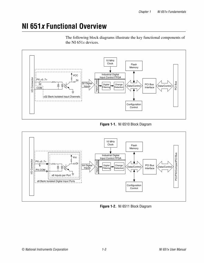
NI 651x Functional OverviewThe following block diagrams illustrate the key functional components of the NI 651x devices.
Figure 1-1. NI 6510 Block Diagram
Figure 1-2. NI 6511 Block Diagram
PC
I Bus
Industrial DigitalInput Control FPGA
Inpu
t Lin
es
ChangeDetection
DigitalFiltering Data/Control
PCI BusInterface
Data/Control
FlashMemory
ConfigurationControl
I/O C
onne
ctor
32
COM
PX.<0..7>
VCC
x32 Bank Isolated Input Channels
DI
10 MHzClock
32 DigitalInputs
I/O C
onne
ctor
PC
I/PX
I/Com
pact
PC
I BusIndustrial Digital
Input Control FPGA
Inpu
t Lin
es
ChangeDetection
DigitalFiltering Data/Control
PCI BusInterface
Data/Control
FlashMemory
ConfigurationControl
8
PX.COM
PX.<0..7>
Vcc
x8 Bank Isolated Digital Input Ports
x8 Inputs per Port
DI
10 MHzClock
64 DigitalInputs

Chapter 1 NI 651x Fundamentals
NI 651x User Manual 1-4 ni.com
Figure 1-3. NI 6512 Block Diagram
Figure 1-4. NI 6513 Block Diagram
Industrial DigitalOutput Control FPGA
Out
put L
ines Programmable
Power-Up States
Watchdog Timer
64 DigitalOutputs
PX.COM
PX.Vcc
PX.<0..7>8
x8 Bank Isolated Digital Output Ports
PC
I/PX
I/Com
pact
PC
I Bus
10 MHzClock
Data/ControlPCI BusInterface
Data/Control
FlashMemory
ConfigurationControl
DO
x8 Outputs per Port
VoltageRegulator
I/O C
onne
ctor
I/O C
onne
ctor PX.COM (Vcc)
PX.<0..7>
PX.GND
DO
x8 Outputs per Port
x8 Bank Isolated Digital Output Ports
Industrial DigitalOutput Control FPGA
Out
put L
ines Programmable
Power-Up States
Watchdog Timer
PC
I/PX
I/Com
pact
PC
I Bus
Data/ControlPCI BusInterface
Data/Control
FlashMemory
ConfigurationControl
VoltageRegulator
64 DigitalOutputs
10 MHzClock
Chapter 1 NI 651x Fundamentals
© National Instruments Corporation 1-5 NI 651x User Manual
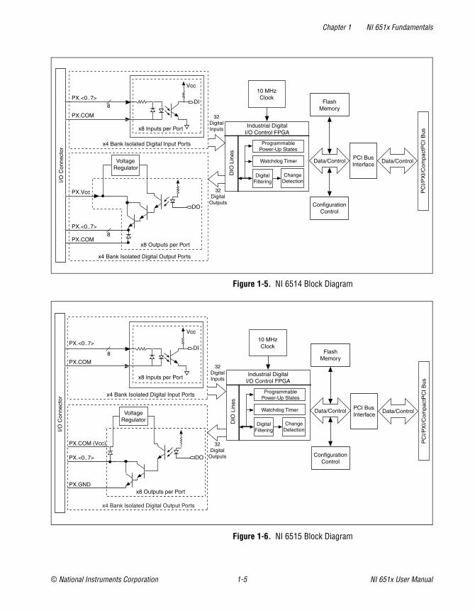
Figure 1-5. NI 6514 Block Diagram
Figure 1-6. NI 6515 Block Diagram
PX.Vcc
PX.<0..7>
PX.COM8
x4 Bank Isolated Digital Output Ports
PC
I/PX
I/Com
pact
PC
I Bus
Data/ControlPCI BusInterface
Data/Control
FlashMemory
ConfigurationControl
10 MHzClock
32Digital
Outputs
Industrial DigitalI/O Control FPGA
DIO
Lin
es
ProgrammablePower-Up States
Watchdog Timer
ChangeDetection
DigitalFiltering
32DigitalInputs
I/O C
onne
ctor
8
PX.COM
PX.<0..7>
Vcc
x4 Bank Isolated Digital Input Ports
x8 Inputs per Port
DI
DO
x8 Outputs per Port
VoltageRegulator
PX.COM (Vcc)
PX.<0..7>
PX.GND
DO
x8 Outputs per Port
x4 Bank Isolated Digital Output Ports
PC
I/PX
I/Com
pact
PC
I Bus
Data/ControlPCI BusInterface
10 MHzClock
32Digital
Outputs
32DigitalInputs
I/O C
onne
ctor
8
PX.COM
PX.<0..7>
Vcc
x4 Bank Isolated Digital Input Ports
x8 Inputs per Port
DI
Industrial DigitalI/O Control FPGA
DIO
Lin
es
ProgrammablePower-Up States
Watchdog Timer
ChangeDetection
DigitalFiltering
Data/Control
FlashMemory
ConfigurationControl
VoltageRegulator

Chapter 1 NI 651x Fundamentals
NI 651x User Manual 1-6 ni.com
Figure 1-7. NI 6516 Block Diagram
Figure 1-8. NI 6517 Block Diagram
Industrial DigitalOutput Control FPGA
Out
put L
ines Programmable
Power-Up States
Watchdog Timer PC
I Bus
10 MHzClock
Data/ControlPCI BusInterface
Data/Control
FlashMemory
ConfigurationControl
COM.GND
VCC
PX.<0..7>
32
DO
x32 Bank Isolated Output Channels
VoltageRegulator
I/O C
onne
ctor
32 DigitalOutputs
Industrial DigitalOutput Control FPGA
Out
put L
ines Programmable
Power-Up States
Watchdog Timer PC
I Bus
10 MHzClock
Data/ControlPCI BusInterface
Data/Control
FlashMemory
ConfigurationControl
I/O C
onne
ctor COM (VCC)
PX.<0..7>
GND
DO
x32 Bank Isolated Output Channels
VoltageRegulator
32 DigitalOutputs

Chapter 1 NI 651x Fundamentals
© National Instruments Corporation 1-7 NI 651x User Manual
Figure 1-9. NI 6518 Block Diagram
Figure 1-10. NI 6519 Block Diagram
VCC
P<2..3>.<0..7>
OUT.COM (GND)
16
PC
I Bus
Data/ControlPCI BusInterface
Data/Control
FlashMemory
ConfigurationControl
10 MHzClock
Industrial DigitalI/O Control FPGA
DIO
Lin
es
ProgrammablePower-Up States
Watchdog Timer
ChangeDetection
DigitalFilteringI/O
Con
nect
or
16
IN.COM
P<0..1>.<0..7>
VCC
x16 Bank IsolatedInput Channels
DI
DO
x16 Bank IsolatedOutput Channels
VoltageRegulator
16Digital
Outputs
16DigitalInputs
I/O C
onne
ctor
PC
I Bus
Data/ControlPCI BusInterface
10 MHzClock
16
IN.COM
P<1..2>.<0..7>
VCC
x16 Bank Isolated Input Channels
DI
Industrial DigitalI/O Control FPGA
DIO
Lin
es
ProgrammablePower-Up States
Watchdog Timer
ChangeDetection
DigitalFiltering
Data/Control
FlashMemory
ConfigurationControl
OUT.COM (VCC)
P<2..3>.<0..7>
GND
DO
VoltageRegulator
x16 Bank Isolated Output Channels
16
16DigitalInputs
16Digital
Outputs

© National Instruments Corporation 2-1 NI 651x User Manual
2NI 651x Features
This chapter describes the National Instruments digital I/O features available for NI 651x devices. For more information on the NI industrial DIO feature set, refer to the Complete Industrial Digital I/O and Counter/Timer Tutorial. To access this tutorial, visit ni.com/info and enter the code rdcidi.
Digital FilteringUse the digital filter option available on the NI 651x input lines to eliminate glitches on input data. When used with change detection, filtering can also reduce the number of changes to examine and process.
You can configure the digital input channels to pass through a digital filter after the photocouplers, and you can control the timing interval the filter uses. The filter blocks pulses that are shorter than half of the specified timing interval and passes pulses that are longer than the specified interval. Intermediate-length pulses—pulses longer than half of the interval but less than the interval—may or may not pass the filter.
The filter operates on the inputs from the photocouplers. Photocouplers turn on faster than they turn off and pass rising edges faster than falling edges.
Table 2-1 lists the pulse widths guaranteed to be passed and blocked.
You can enable filtering on as many input lines as is necessary for your application. All filtered lines share the same timing interval, which ranges from 200 μs to 200 ms.
Table 2-1. NI 651x Digital Filter Timing Intervals
Filter Interval
Pulse Width Passed Pulse Width Blocked
Low Pulse High Pulse Low Pulse High Pulse
tinterval tinterval + 200 μs tinterval tinterval/2 (tinterval/2) – 200 μs
Chapter 2 NI 651x Features
NI 651x User Manual 2-2 ni.com
Internally, the filter uses two clocks: the sample clock and the filter clock. The sample clock has a 100 ns period. The filter clock is generated by a counter and has a period equal to one half of the specified timing interval. The input signal is sampled on each rising edge of the sample clock, which is every 100 ns. However, a change in the input signal is recognized only if it maintains its new state for at least two consecutive rising edges of the filter clock.
The filter clock is programmable and allows you to control how long a pulse must last to be recognized. The sample clock provides a fast sample rate to ensure that input pulses remain constant between filter clocks.
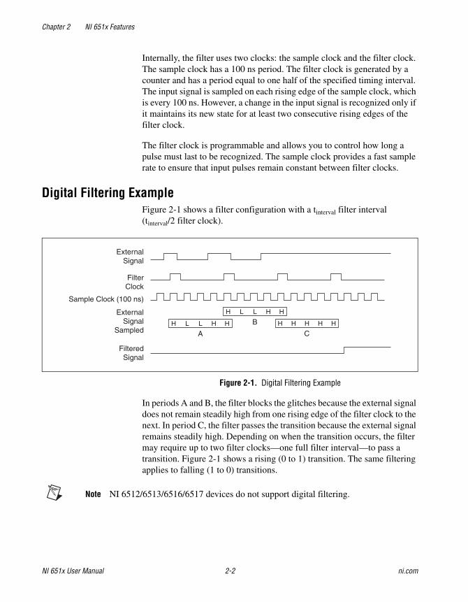
Digital Filtering ExampleFigure 2-1 shows a filter configuration with a tinterval filter interval(tinterval/2 filter clock).
Figure 2-1. Digital Filtering Example
In periods A and B, the filter blocks the glitches because the external signal does not remain steadily high from one rising edge of the filter clock to the next. In period C, the filter passes the transition because the external signal remains steadily high. Depending on when the transition occurs, the filter may require up to two filter clocks—one full filter interval—to pass a transition. Figure 2-1 shows a rising (0 to 1) transition. The same filtering applies to falling (1 to 0) transitions.
Note NI 6512/6513/6516/6517 devices do not support digital filtering.
ExternalSignal
ExternalSignal
Sampled
FilterClock
Sample Clock (100 ns)
FilteredSignal
H H H H HH L L H H
H L L H H
A
B
C

Chapter 2 NI 651x Features
© National Instruments Corporation 2-3 NI 651x User Manual
Programmable Power-Up StatesAt power-up, the output drives on the NI 651x device is disabled. All output lines are user-configurable for an on or off state. User-configurable power-up states are useful for ensuring that the NI 651x device powers up in a known state.
To use MAX (recommended) to program the power-up states, select the device and click the Properties button. Refer to the software documentation for information about how to program the power-up states using NI-DAQ with LabVIEW or other National Instruments application development environments (ADEs).
Note The response time of programmable power-up states is 400 ms.
Note NI 6510/6511 devices do not support programmable power-up states.
Change DetectionYou can program NI 651x devices to send an interrupt when a change occurs on any input line.
The DIO device can monitor changes on selected input lines or on all input lines. It can monitor for rising edges (0 to 1), falling edges (1 to 0), or both. When an input change occurs, the DIO device generates an interrupt, and the NI-DAQ driver then notifies the software.
Note Excessive change detections can affect system performance. Use digital filtering to minimize the effects of noisy input lines.
The DIO device sends a change detection when any one of the changes occurs, but it does not report which line changed or if the line was rising or falling. After a change, you can read the input lines to determine the current line states. The maximum rate of change detection is determined by the software response time, which varies from system to system.
An overflow bit indicates that an additional rising or falling edge has been detected before the software could process the previous change.
Refer to the software documentation for information about how to set up and implement the change detection.
Chapter 2 NI 651x Features
NI 651x User Manual 2-4 ni.com
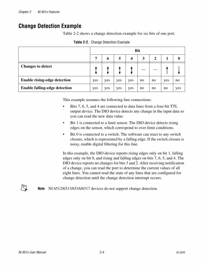
Change Detection ExampleTable 2-2 shows a change detection example for six bits of one port.
This example assumes the following line connections:
• Bits 7, 6, 5, and 4 are connected to data lines from a four-bit TTL output device. The DIO device detects any change in the input data so you can read the new data value.
• Bit 1 is connected to a limit sensor. The DIO device detects rising edges on the sensor, which correspond to over-limit conditions.
• Bit 0 is connected to a switch. The software can react to any switch closure, which is represented by a falling edge. If the switch closure is noisy, enable digital filtering for this line.
In this example, the DIO device reports rising edges only on bit 1, falling edges only on bit 0, and rising and falling edges on bits 7, 6, 5, and 4. The DIO device reports no changes for bits 3 and 2. After receiving notification of a change, you can read the port to determine the current values of all eight lines. You cannot read the state of any lines that are configured for change detection until the change detection interrupt occurs.
Note NI 6512/6513/6516/6517 devices do not support change detection.
Table 2-2. Change Detection Example
Bit
7 6 5 4 3 2 1 0
Changes to detect— —
Enable rising-edge detection yes yes yes yes no no yes no
Enable falling-edge detection yes yes yes yes no no no yes

Chapter 2 NI 651x Features
© National Instruments Corporation 2-5 NI 651x User Manual
Watchdog TimerThe watchdog timer is a software configurable feature used to set critical outputs to safe states in the event of a software failure, a system crash, or any other loss of communication between the application and the NI 651x device.
When the watchdog timer is enabled, if the NI 651x device does not receive a watchdog reset software command within the time specified for the watchdog timer, the outputs go to a user-defined safe state and remain in that state until the watchdog timer is disarmed by the application and new values are written, the NI 651x device is reset, or the computer is restarted. The expiration signal that indicates an expired watchdog will continue to assert until the watchdog is disarmed. After the watchdog timer expires, the NI 651x device ignores any writes until the watchdog timer is disarmed.
You can set the watchdog timer timeout period to specify the amount of time that must elapse before the watchdog timer expires. The counter on the watchdog timer is configurable up to (232 – 1) × 100 ns (approximately seven minutes) before it expires.
Note NI 6510/6511 devices do not support the watchdog timer.

© National Instruments Corporation 3-1 NI 651x User Manual
3Digital I/O
I/O Connector
NI 6510 I/O ConnectorThe 37-pin D-SUB connector on the NI 6510 provides access to the digital inputs. The digital I/O available on this connector includes 32 inputs. For easy connection to the digital I/O connector, use the National Instruments SH37F-37M shielded digital I/O cable with the CB-37F connector block. For more information on digital I/O connectivity options, refer to Chapter 5, Cables and Accessories.
Caution Do not make connections to the digital I/O that exceed the maximum I/O specifications. Doing so could permanently damage the NI 6510 and the computer. Refer to the NI 651x Specifications, available at ni.com/manuals, for information about maximum input ratings.
The input lines on the NI 6510 consist of input photocouplers, which react to a voltage differential rather than only to a voltage increase. If the voltage connected to a digital input is either greater than or less than the voltage connected to COM by at least the logic threshold, the reading on the digital line will be logic high, even though in one instance the digital line has a lower voltage level than COM.
For more information, refer to the Pin Assignments section.
NI 6511 I/O ConnectorThe 100-pin high-density SCSI connector on the NI 6511 provides access to the digital inputs. The digital I/O available on this connector includes 64 inputs. For easy connection to the digital I/O connector, use the National Instruments SH100-100-F shielded digital I/O cable with the SCB-100 connector block, or use the R1005050 ribbon cable with the CB-50 or CB-50LP connector block. For more information on digital I/O connectivity options, refer to Chapter 5, Cables and Accessories.

Chapter 3 Digital I/O
NI 651x User Manual 3-2 ni.com
Caution Do not make connections to the digital I/O that exceed the maximum I/O specifications. Doing so could permanently damage the NI 6511 and the computer. Refer to the NI 651x Specifications, available at ni.com/manuals, for information about maximum input ratings.
The input lines on the NI 6511 consist of input photocouplers, which react to a voltage differential rather than only to a voltage increase. If the voltage connected to a digital input is either greater than or less than the voltage connected to PX.COM by at least the logic threshold, the reading on the digital line will be logic high, even though in one instance the digital line has a lower voltage level than PX.COM.
For more information, refer to the Pin Assignments section.
NI 6512/6513 I/O ConnectorThe 100-pin high-density SCSI connector on the NI 6512/6513 provides access to the digital inputs and outputs. The digital I/O available on this connector includes 64 outputs. For easy connection to the digital I/O connector, use the National Instruments SH100-100-F shielded digital I/O cable with the SCB-100 connector block, or use the R1005050 ribbon cable with the CB-50 or CB-50LP connector block. For more information on digital I/O connectivity options, refer to Chapter 5, Cables and Accessories.
Caution Do not make connections to the digital I/O that exceed the maximum I/O specifications. Doing so could permanently damage the NI 6512/6513 and the computer. Refer to the NI 651x Specifications, available at ni.com/manuals, for information about maximum input ratings.
The output lines on the NI 6512 consist of photocouplers and Darlington arrays. To connect to these signals, connect a 5 V to 30 V power supply to VCC, connect COM to ground, and cross a load between digital output and COM.
The output lines on the NI 6513 consist of photocouplers and Darlington arrays. To connect to these signals, connect a 5 V to 30 V power supply to COM, connect GND to ground, and cross a load between digital output and COM.
For more information, refer to the Pin Assignments section.

Chapter 3 Digital I/O
© National Instruments Corporation 3-3 NI 651x User Manual
NI 6514/6515 I/O ConnectorThe 100-pin high-density SCSI connector on the NI 6514/6515 provides access to the digital inputs and outputs. The digital I/O available on this connector includes 32 inputs and 32 outputs. For easy connection to the digital I/O connector, use the National Instruments SH100-100-F shielded digital I/O cable with the SCB-100 connector block, or use the R1005050 ribbon cable with the CB-50 or CB-50LP connector block. For more information on digital I/O connectivity options, refer to Chapter 5, Cables and Accessories.
Caution Do not make connections to the digital I/O that exceed the maximum I/O specifications. Doing so could permanently damage the NI 6514/6515 and the computer. Refer to the NI 651x Specifications, available at ni.com/manuals, for information about maximum input ratings.
The input lines on the NI 6514/6515 consist of input photocouplers, which react to a voltage differential rather than only to a voltage increase. If the voltage connected to a digital input is either greater than or less than the voltage connected to PX.COM by at least the logic threshold, the reading on the digital line will be logic high, even though in one instance the digital line has a lower voltage level than PX.COM.
The output lines on the NI 6515 consist of photocouplers and Darlington arrays. To connect to these signals, connect a 5 V to 30 V power supply to COM, connect GND to ground, and cross a load between digital output and COM.
For more information, refer to the Pin Assignments section.
NI 6516/6517 I/O ConnectorThe 37-pin D-SUB connector on the NI 6516/6517 provides access to the digital inputs and outputs. The digital I/O available on this connector includes 32 outputs. For easy connection to the digital I/O connector, use the National Instruments SH37F-37M shielded digital I/O cable with the CB-37F connector block. For more information on digital I/O connectivity options, refer to Chapter 5, Cables and Accessories.
Caution Do not make connections to the digital I/O that exceed the maximum I/O specifications. Doing so could permanently damage the NI 6516/6517 and the computer. Refer to the NI 651x Specifications, available at ni.com/manuals, for information about maximum input ratings.

Chapter 3 Digital I/O
NI 651x User Manual 3-4 ni.com
The output lines on the NI 6516 consist of photocouplers and Darlington arrays. To connect to these signals, connect a 5 V to 30 V power supply to VCC, connect COM (GND) to ground, and cross a load between digital output and COM (GND).
The output lines on the NI 6517 consist of photocouplers and Darlington arrays. To connect to these signals, connect a 5 V to 30 V power supply to COM (VCC), connect GND to ground, and cross a load between digital output and COM (VCC).
For more information, refer to the Pin Assignments section.
NI 6518/6519 I/O ConnectorThe 37-pin D-SUB connector on the NI 6518/6519 provides access to the digital inputs and outputs. The digital I/O available on this connector includes 32 inputs and 32 outputs. For easy connection to the digital I/O connector, use the National Instruments SH37F-37M shielded digital I/O cable with the CB-37F connector block. For more information on digital I/O connectivity options, refer to Chapter 5, Cables and Accessories.
Caution Do not make connections to the digital I/O that exceed the maximum I/O specifications. Doing so could permanently damage the NI 6518/6519 and the computer. Refer to the NI 651x Specifications, available at ni.com/manuals, for information about maximum input ratings.
The input lines on the NI 6518/6519 consist of input photocouplers, which react to a voltage differential rather than only to a voltage increase. If the voltage connected to a digital input is either greater than or less than the voltage connected to IN.COM by at least the logic threshold, the reading on the digital line will be logic high, even though in one instance the digital line has a lower voltage level than IN.COM.
The output lines on the NI 6518/6519 consist of photocouplers and Darlington arrays. To connect to these signals, connect a 5 V to 30 V power supply to IN.COM, connect COM (GND) to ground, and cross a load between digital output and IN.COM.
For more information, refer to the Pin Assignments section.

Chapter 3 Digital I/O
© National Instruments Corporation 3-5 NI 651x User Manual
Pin Assignments
NI 6510 Pin AssignmentsFigure 3-1 shows the pin assignments for the SH37F-37M cable when connecting to the NI 6510 device. The naming convention for each pin is PX.Y, where X is the port (P) number, and Y is the line number or name.
Figure 3-1. NI 6510 Pin Assignments
For more information on the NI 6510 signals, refer to the Signal Descriptions section.
NI 6511 SH100-100-F Pin AssignmentsFigure 3-2 shows the pin assignments for the SH100-100-F cable when connecting to the NI 6511 device. The naming convention for each pin is PX.Y, where X is the port (P) number, and Y is the line number or name.
1
2
3
4
5
6
7
8
9
10
11
12
13
14
15
16
17
18
19
20
21
22
23
24
25
26
27
28
29
30
31
32
33
34
35
36
37
P0.0
P0.2
P0.4
P0.6
COM
P1.1
P1.3
P1.5
P1.7
P2.0
P2.2
P2.4
P2.6
COM
P3.1
P3.3
P3.5
P3.7
COM
P0.1
P0.3
P0.5
P0.7
P1.0
P1.2
P1.4
P1.6
COM
P2.1
P2.3
P2.5
P2.7
P3.0
P3.2
P3.4
P3.6
COM

Chapter 3 Digital I/O
NI 651x User Manual 3-6 ni.com
Figure 3-2. NI 6511 Pin Assignments for the SH100-100-F Cable
25
24
23
22
21
20
19
18
17
16
15
14
13
12
11
10
9
8
7
6
5
4
3
2
1
75
74
73
72
71
70
69
68
67
66
65
64
63
62
61
60
59
58
57
56
55
54
53
52
51
50
49
48
47
46
45
44
43
42
41
40
39
38
37
36
35
34
33
32
31
30
29
28
27
26
100
99
98
97
96
95
94
93
92
91
90
89
88
87
86
85
84
83
82
81
80
79
78
77
76
NC
P6.COM
P6.COM
P6.COM
P6.COM
P6.7
P6.6
P6.5
P6.4
P6.3
P6.2
P6.1
P6.0
P4.COM
P4.COM
P4.COM
P4.COM
P4.7
P4.6
P4.5
P4.4
P4.3
P4.2
P4.1
P4.0
NC
P2.COM
P2.COM
P2.COM
P2.COM
P2.7
P2.6
P2.5
P2.4
P2.3
P2.2
P2.1
P2.0
P0.COM
P0.COM
P0.COM
P0.COM
P0.7
P0.6
P0.5
P0.4
P0.3
P0.2
P0.1
P0.0
NC
P7.COM
P7.COM
P7.COM
P7.COM
P7.7
P7.6
P7.5
P7.4
P7.3
P7.2
P7.1
P7.0
P5.COM
P5.COM
P5.COM
P5.COM
P5.7
P5.6
P5.5
P5.4
P5.3
P5.2
P5.1
P5.0
NC
P3.COM
P3.COM
P3.COM
P3.COM
P3.7
P3.6
P3.5
P3.4
P3.3
P3.2
P3.1
P3.0
P1.COM
P1.COM
P1.COM
P1.COM
P1.7
P1.6
P1.5
P1.4
P1.3
P1.2
P1.1
P1.0
NC = No Connect

Chapter 3 Digital I/O
© National Instruments Corporation 3-7 NI 651x User Manual
For more information on the NI 6511 signals, refer to the Signal Descriptions section.
NI 6511 R1005050 Pin AssignmentsFigure 3-3 shows the pin assignments for the R1005050 cable when connecting to the NI 6511 device. The naming convention for each pin is PX.Y, where X is the port (P) number, and Y is the line number or name.
Figure 3-3. NI 6511 Pin Assignments for the R1005050 Cable
For more information on the NI 6511 signals, refer to the Signal Descriptions section.
P6.COM
P6.COM
P6.7
P6.5
P6.3
P6.1
P4.COM
P4.COM
P4.7
P4.5
P4.3
P4.1
NC
P2.COM
P2.COM
P2.6
P2.4
P2.2
P2.0
P0.COM
P0.COM
P0.6
P0.4
P0.2
P0.0
NC
P6.COM (P6.GND)
P6.6
P6.2
P6.0
P4.COM
P4.COM
P6.COM
P6.4
P4.6
P4.4
P4.2
P4.0
P2.COM
P2.COM
P2.7
P2.5
P2.3
P2.1
P0.COM
P0.COM
P0.7
P0.5
P0.3
P0.1
49 50
47 48
45 46
43 44
41 42
39 40
37 38
35 36
33 34
31 32
29 30
27 28
25 26
23 24
21 22
19 20
17 18
15 16
13 14
11 12
9 10
7 8
5 6
3 4
1 2
Positions 51 through 100
49 50
47 48
45 46
43 44
41 42
39 40
37 38
35 36
33 34
31 32
29 30
27 28
25 26
23 24
21 22
19 20
17 18
15 16
13 14
11 12
9 10
7 8
5 6
3 4
1 2
P7.COM
P7.COM
P7.7
P7.5
P7.3
P7.1
P5.COM
P5.COM
P5.7
P5.5
P5.3
P5.1
NC
P3.COM
P3.COM
P3.6
P3.4
P3.2
P3.0
P1.COM
P1.COM
P1.6
P1.4
P1.2
P1.0
NC
P7.COM
P7.6
P7.2
P7.0
P5.COM
P5.COM
P7.COM
P7.4
P5.6
P5.4
P5.2
P5.0
P3.COM
P3.COM
P3.7
P3.5
P3.3
P3.1
P1.COM
P1.COM
P1.7
P1.5
P1.3
P1.1
Positions 1 through 50
NC = No Connect

Chapter 3 Digital I/O
NI 651x User Manual 3-8 ni.com
NI 6512 SH100-100-F Pin AssignmentsFigure 3-4 shows the pin assignments for the SH100-100-F cable when connecting to the NI 6512 device. The naming convention for each pin is PX.Y, where X is the port (P) number, and Y is the line number or name.

Chapter 3 Digital I/O
© National Instruments Corporation 3-9 NI 651x User Manual
Figure 3-4. NI 6512 Pin Assignments for the SH100-100-F Cable
25
24
23
22
21
20
19
18
17
16
15
14
13
12
11
10
9
8
7
6
5
4
3
2
1
75
74
73
72
71
70
69
68
67
66
65
64
63
62
61
60
59
58
57
56
55
54
53
52
51
50
49
48
47
46
45
44
43
42
41
40
39
38
37
36
35
34
33
32
31
30
29
28
27
26
100
99
98
97
96
95
94
93
92
91
90
89
88
87
86
85
84
83
82
81
80
79
78
77
76
P6.+5V
P6.VCC
P6.VCC
P6.VCC
P6.COM (P6.GND)
P6.7
P6.6
P6.5
P6.4
P6.3
P6.2
P6.1
P6.0
P4.VCC
P4.VCC
P4.VCC
P4.COM (P4.GND)
P4.7
P4.6
P4.5
P4.4
P4.3
P4.2
P4.1
P4.0
NC
P2.VCC
P2.VCC
P2.VCC
P2.COM (P2.GND)
P2.7
P2.6
P2.5
P2.4
P2.3
P2.2
P2.1
P2.0
P0.VCC
P0.VCC
P0.VCC
P0.COM (P0.GND)
P0.7
P0.6
P0.5
P0.4
P0.3
P0.2
P0.1
P0.0
P7.+5V
P7.VCC
P7.VCC
P7.VCC
P7.COM (P7.GND)
P7.7
P7.6
P7.5
P7.4
P7.3
P7.2
P7.1
P7.0
P5.VCC
P5.VCC
P5.VCC
P5.COM (P5.GND)
P5.7
P5.6
P5.5
P5.4
P5.3
P5.2
P5.1
P5.0
NC
P3.VCC
P3.VCC
P3.VCC
P3.COM (P3.GND)
P3.7
P3.6
P3.5
P3.4
P3.3
P3.2
P3.1
P3.0
P1.VCC
P1.VCC
P1.VCC
P1.COM (P1.GND)
P1.7
P1.6
P1.5
P1.4
P1.3
P1.2
P1.1
P1.0
NC = No Connect
Chapter 3 Digital I/O
NI 651x User Manual 3-10 ni.com
For more information on the NI 6512 signals, refer to the Signal Descriptions section.
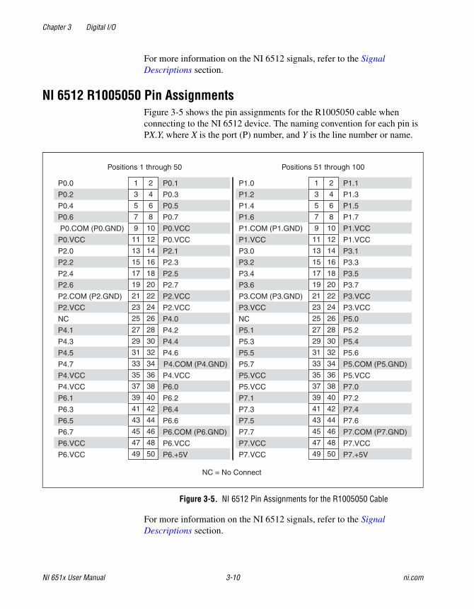
NI 6512 R1005050 Pin AssignmentsFigure 3-5 shows the pin assignments for the R1005050 cable when connecting to the NI 6512 device. The naming convention for each pin is PX.Y, where X is the port (P) number, and Y is the line number or name.
Figure 3-5. NI 6512 Pin Assignments for the R1005050 Cable
For more information on the NI 6512 signals, refer to the Signal Descriptions section.
P6.VCC
P6.VCC
P6.7
P6.5
P6.3
P6.1
P4.VCC
P4.VCC
P4.7
P4.5
P4.3
P4.1
NC
P2.VCC
P2.COM (P2.GND)
P2.6
P2.4
P2.2
P2.0
P0.VCC
P0.COM (P0.GND)
P0.6
P0.4
P0.2
P0.0
P6.+5V
P6.COM (P6.GND)
P6.6
P6.2
P6.0
P4.VCC
P4.COM (P4.GND)
P6.VCC
P6.4
P4.6
P4.4
P4.2
P4.0
P2.VCC
P2.VCC
P2.7
P2.5
P2.3
P2.1
P0.VCC
P0.VCC
P0.7
P0.5
P0.3
P0.1
49 50
47 48
45 46
43 44
41 42
39 40
37 38
35 36
33 34
31 32
29 30
27 28
25 26
23 24
21 22
19 20
17 18
15 16
13 14
11 12
9 10
7 8
5 6
3 4
1 2
Positions 1 through 50 Positions 51 through 100
49 50
47 48
45 46
43 44
41 42
39 40
37 38
35 36
33 34
31 32
29 30
27 28
25 26
23 24
21 22
19 20
17 18
15 16
13 14
11 12
9 10
7 8
5 6
3 4
1 2
P7.VCC
P7.VCC
P7.7
P7.5
P7.3
P7.1
P5.VCC
P5.VCC
P5.7
P5.5
P5.3
P5.1
NC
P3.VCC
P3.COM (P3.GND)
P3.6
P3.4
P3.2
P3.0
P1.VCC
P1.COM (P1.GND)
P1.6
P1.4
P1.2
P1.0
P7.+5V
P7.COM (P7.GND)
P7.6
P7.2
P7.0
P5.VCC
P5.COM (P5.GND)
P7.VCC
P7.4
P5.6
P5.4
P5.2
P5.0
P3.VCC
P3.VCC
P3.7
P3.5
P3.3
P3.1
P1.VCC
P1.VCC
P1.7
P1.5
P1.3
P1.1
NC = No Connect

Chapter 3 Digital I/O
© National Instruments Corporation 3-11 NI 651x User Manual
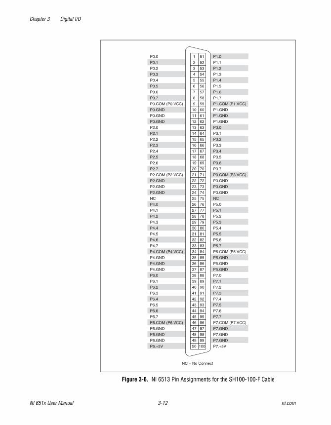
NI 6513 SH100-100-F Pin AssignmentsFigure 3-6 shows the pin assignments for the SH100-100-F cable when connecting to the NI 6513 device. The naming convention for each pin is PX.Y, where X is the port (P) number, and Y is the line number or name.
Chapter 3 Digital I/O
NI 651x User Manual 3-12 ni.com
Figure 3-6. NI 6513 Pin Assignments for the SH100-100-F Cable
25
24
23
22
21
20
19
18
17
16
15
14
13
12
11
10
9
8
7
6
5
4
3
2
1
75
74
73
72
71
70
69
68
67
66
65
64
63
62
61
60
59
58
57
56
55
54
53
52
51
50
49
48
47
46
45
44
43
42
41
40
39
38
37
36
35
34
33
32
31
30
29
28
27
26
100
99
98
97
96
95
94
93
92
91
90
89
88
87
86
85
84
83
82
81
80
79
78
77
76
P6.+5V
P6.GND
P6.GND
P6.GND
P6.COM (P6.VCC)
P6.7
P6.6
P6.5
P6.4
P6.3
P6.2
P6.1
P6.0
P4.GND
P4.GND
P4.GND
P4.COM (P4.VCC)
P4.7
P4.6
P4.5
P4.4
P4.3
P4.2
P4.1
P4.0
NC
P2.GND
P2.GND
P2.GND
P2.COM (P2.VCC)
P2.7
P2.6
P2.5
P2.4
P2.3
P2.2
P2.1
P2.0
P0.GND
P0.GND
P0.GND
P0.COM (P0.VCC)
P0.7
P0.6
P0.5
P0.4
P0.3
P0.2
P0.1
P0.0
P7.+5V
P7.GND
P7.GND
P7.GND
P7.COM (P7.VCC)
P7.7
P7.6
P7.5
P7.4
P7.3
P7.2
P7.1
P7.0
P5.GND
P5.GND
P5.GND
P5.COM (P5.VCC)
P5.7
P5.6
P5.5
P5.4
P5.3
P5.2
P5.1
P5.0
NC
P3.GND
P3.GND
P3.GND
P3.COM (P3.VCC)
P3.7
P3.6
P3.5
P3.4
P3.3
P3.2
P3.1
P3.0
P1.GND
P1.GND
P1.GND
P1.COM (P1.VCC)
P1.7
P1.6
P1.5
P1.4
P1.3
P1.2
P1.1
P1.0
NC = No Connect

Chapter 3 Digital I/O
© National Instruments Corporation 3-13 NI 651x User Manual
For more information on the NI 6513 signals, refer to the Signal Descriptions section.
NI 6513 R1005050 Pin AssignmentsFigure 3-7 shows the pin assignments for the R1005050 cable when connecting to the NI 6513 device. The naming convention for each pin is PX.Y, where X is the port (P) number, and Y is the line number or name.
Figure 3-7. NI 6513 Pin Assignments for the R1005050 Cable
For more information on the NI 6513 signals, refer to the Signal Descriptions section.
P6.GND
P6.GND
P6.7
P6.5
P6.3
P6.1
P4.GND
P4.GND
P4.7
P4.5
P4.3
P4.1
NC
P2.GND
P2.COM (P2.VCC)
P2.6
P2.4
P2.2
P2.0
P0.GND
P0.COM (P0.VCC)
P0.6
P0.4
P0.2
P0.0
P6.+5V
P6.COM (P6.VCC)
P6.6
P6.2
P6.0
P4.GND
P4.COM (P4.VCC)
P6.GND
P6.4
P4.6
P4.4
P4.2
P4.0
P2.GND
P2.GND
P2.7
P2.5
P2.3
P2.1
P0.GND
P0.GND
P0.7
P0.5
P0.3
P0.1
49 50
47 48
45 46
43 44
41 42
39 40
37 38
35 36
33 34
31 32
29 30
27 28
25 26
23 24
21 22
19 20
17 18
15 16
13 14
11 12
9 10
7 8
5 6
3 4
1 2
Positions 1 through 50 Positions 51 through 100
49 50
47 48
45 46
43 44
41 42
39 40
37 38
35 36
33 34
31 32
29 30
27 28
25 26
23 24
21 22
19 20
17 18
15 16
13 14
11 12
9 10
7 8
5 6
3 4
1 2
P7.GND
P7.GND
P7.7
P7.5
P7.3
P7.1
P5.GND
P5.GND
P5.7
P5.5
P5.3
P5.1
NCP3.GND
P3.COM (P3.VCC)
P3.6
P3.4
P3.2
P3.0
P1.GND
P1.COM (P1.VCC)
P1.6
P1.4
P1.2
P1.0
P7.+5V
P7.COM (P7.VCC)
P7.6
P7.2
P7.0
P5.GND
P5.COM (P5.VCC)
P7.GND
P7.4
P5.6
P5.4
P5.2
P5.0
P3.GND
P3.GND
P3.7
P3.5
P3.3
P3.1
P1.GND
P1.GND
P1.7
P1.5
P1.3
P1.1
NC = No Connect

Chapter 3 Digital I/O
NI 651x User Manual 3-14 ni.com
NI 6514 SH100-100-F Pin AssignmentsFigure 3-8 shows the pin assignments for the SH100-100-F cable when connecting to the NI 6514 device. The naming convention for each pin is PX.Y, where X is the port (P) number, and Y is the line number or name.

Chapter 3 Digital I/O
© National Instruments Corporation 3-15 NI 651x User Manual
Figure 3-8. NI 6514 Pin Assignments for the SH100-100-F Cable
P6.+5V
P6.VCC
P6.VCC
P6.VCC
P6.COM (P6.GND)
P6.7
P6.6
P6.5
P6.4
P6.3
P6.2
P6.1
P6.0
P4.VCC
P4.VCC
P4.VCC
P4.COM (P4.GND)
P4.7
P4.6
P4.5
P4.4
P4.3
P4.2
P4.1
P4.0
NC
P2.COM
P2.COM
P2.COM
P2.COM
P2.7
P2.6
P2.5
P2.4
P2.3
P2.2
P2.1
P2.0
P0.COM
P0.COM
P0.COM
P0.COM
P0.7
P0.6
P0.5
P0.4
P0.3
P0.2
P0.1
P0.0
P7.+5V
P7.VCC
P7.VCC
P7.VCC
P7.COM (P7.GND)
P7.7
P7.6
P7.5
P7.4
P7.3
P7.2
P7.1
P7.0
P5.VCC
P5.VCC
P5.VCC
P5.COM (P5.GND)
P5.7
P5.6
P5.5
P5.4
P5.3
P5.2
P5.1
P5.0
NC
P3.COM
P3.COM
P3.COM
P3.COM
P3.7
P3.6
P3.5
P3.4
P3.3
P3.2
P3.1
P3.0
P1.COM
P1.COM
P1.COM
P1.COM
P1.7
P1.6
P1.5
P1.4
P1.3
P1.2
P1.1
P1.0
25
24
23
22
21
20
19
18
17
16
15
14
13
12
11
10
9
8
7
6
5
4
3
2
1
75
74
73
72
71
70
69
68
67
66
65
64
63
62
61
60
59
58
57
56
55
54
53
52
51
50
49
48
47
46
45
44
43
42
41
40
39
38
37
36
35
34
33
32
31
30
29
28
27
26
100
99
98
97
96
95
94
93
92
91
90
89
88
87
86
85
84
83
82
81
80
79
78
77
76
NC = No Connect
Chapter 3 Digital I/O
NI 651x User Manual 3-16 ni.com
For more information on the NI 6514 signals, refer to the Signal Descriptions section.
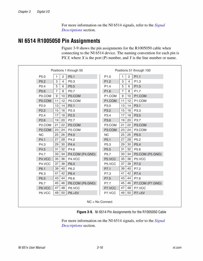
NI 6514 R1005050 Pin AssignmentsFigure 3-9 shows the pin assignments for the R1005050 cable when connecting to the NI 6514 device. The naming convention for each pin is PX.Y, where X is the port (P) number, and Y is the line number or name.
Figure 3-9. NI 6514 Pin Assignments for the R1005050 Cable
For more information on the NI 6514 signals, refer to the Signal Descriptions section.
P6.VCC
P6.VCC
P6.7
P6.5
P6.3
P6.1
P4.VCC
P4.VCC
P4.7
P4.5
P4.3
P4.1
NC
P2.COM
P2.COM
P2.6
P2.4
P2.2
P2.0
P0.COM
P0.COM
P0.6
P0.4
P0.2
P0.0
P6.+5V
P6.COM (P6.GND)
P6.6
P6.2
P6.0
P4.VCC
P4.COM (P4.GND)
P6.VCC
P6.4
P4.6
P4.4
P4.2
P4.0
P2.COM
P2.COM
P2.7
P2.5
P2.3
P2.1
P0.COM
P0.COM
P0.7
P0.5
P0.3
P0.1
49 50
47 48
45 46
43 44
41 42
39 40
37 38
35 36
33 34
31 32
29 30
27 28
25 26
23 24
21 22
19 20
17 18
15 16
13 14
11 12
9 10
7 8
5 6
3 4
1 2
Positions 1 through 50 Positions 51 through 100
49 50
47 48
45 46
43 44
41 42
39 40
37 38
35 36
33 34
31 32
29 30
27 28
25 26
23 24
21 22
19 20
17 18
15 16
13 14
11 12
9 10
7 8
5 6
3 4
1 2
P7.VCC
P7.VCC
P7.7
P7.5
P7.3
P7.1
P5.VCC
P5.VCC
P5.7
P5.5
P5.3
P5.1
NC
P3.COM
P3.COM
P3.6
P3.4
P3.2
P3.0
P1.COM
P1.COM
P1.6
P1.4
P1.2
P1.0
P7.+5V
P7.COM (P7.GND)
P7.6
P7.2
P7.0
P5.VCC
P5.COM (P5.GND)
P7.VCC
P7.4
P5.6
P5.4
P5.2
P5.0
P3.COM
P3.COM
P3.7
P3.5
P3.3
P3.1
P1.COM
P1.COM
P1.7
P1.5
P1.3
P1.1
NC = No Connect

Chapter 3 Digital I/O
© National Instruments Corporation 3-17 NI 651x User Manual
NI 6515 SH100-100-F Pin AssignmentsFigure 3-10 shows the pin assignments for the SH100-100-F cable when connecting to the NI 6515 device. The naming convention for each pin is PX.Y, where X is the port (P) number, and Y is the line number or name.

Chapter 3 Digital I/O
NI 651x User Manual 3-18 ni.com
Figure 3-10. NI 6515 Pin Assignments for the SH100-100-F Cable
P6.+5V
P6.GND
P6.GND
P6.GND
P6.COM (P6.VCC)
P6.7
P6.6
P6.5
P6.4
P6.3
P6.2
P6.1
P6.0
P4.GND
P4.GND
P4.GND
P4.COM (P4.VCC)
P4.7
P4.6
P4.5
P4.4
P4.3
P4.2
P4.1
P4.0
NC
P2.COM
P2.COM
P2.COM
P2.COM
P2.7
P2.6
P2.5
P2.4
P2.3
P2.2
P2.1
P2.0
P0.COM
P0.COM
P0.COM
P0.COM
P0.7
P0.6
P0.5
P0.4
P0.3
P0.2
P0.1
P0.0
P7.+5V
P7.GND
P7.GND
P7.GND
P7.COM (P7.VCC)
P7.7
P7.6
P7.5
P7.4
P7.3
P7.2
P7.1
P7.0
P5.GND
P5.GND
P5.GND
P5.COM (P5.VCC)
P5.7
P5.6
P5.5
P5.4
P5.3
P5.2
P5.1
P5.0
NC
P3.COM
P3.COM
P3.COM
P3.COM
P3.7
P3.6
P3.5
P3.4
P3.3
P3.2
P3.1
P3.0
P1.COM
P1.COM
P1.COM
P1.COM
P1.7
P1.6
P1.5
P1.4
P1.3
P1.2
P1.1
P1.0
25
24
23
22
21
20
19
18
17
16
15
14
13
12
11
10
9
8
7
6
5
4
3
2
1
75
74
73
72
71
70
69
68
67
66
65
64
63
62
61
60
59
58
57
56
55
54
53
52
51
50
49
48
47
46
45
44
43
42
41
40
39
38
37
36
35
34
33
32
31
30
29
28
27
26
100
99
98
97
96
95
94
93
92
91
90
89
88
87
86
85
84
83
82
81
80
79
78
77
76
NC = No Connect

Chapter 3 Digital I/O
© National Instruments Corporation 3-19 NI 651x User Manual
For more information on the NI 6515 signals, refer to the Signal Descriptions section.
NI 6515 R1005050 Pin AssignmentsFigure 3-11 shows the pin assignments for the R1005050 cable when connecting to the NI 6515 device. The naming convention for each pin is PX.Y, where X is the port (P) number, and Y is the line number or name.
Figure 3-11. NI 6515 Pin Assignments for the R1005050 Cable
For more information on the NI 6515 signals, refer to the Signal Descriptions section.
P6.GND
P6.GND
P6.7
P6.5
P6.3
P6.1
P4.GND
P4.GND
P4.7
P4.5
P4.3
P4.1
NC
P2.COM
P2.COM
P2.6
P2.4
P2.2
P2.0
P0.COM
P0.COM
P0.6
P0.4
P0.2
P0.0
P6.+5V
P6.COM (P6.VCC)
P6.6
P6.2
P6.0
P4.GND
P4.COM (P4.VCC)
P6.GND
P6.4
P4.6
P4.4
P4.2
P4.0
P2.COM
P2.COM
P2.7
P2.5
P2.3
P2.1
P0.COM
P0.COM
P0.7
P0.5
P0.3
P0.1
49 50
47 48
45 46
43 44
41 42
39 40
37 38
35 36
33 34
31 32
29 30
27 28
25 26
23 24
21 22
19 20
17 18
15 16
13 14
11 12
9 10
7 8
5 6
3 4
1 2
Positions 1 through 50 Positions 51 through 100
49 50
47 48
45 46
43 44
41 42
39 40
37 38
35 36
33 34
31 32
29 30
27 28
25 26
23 24
21 22
19 20
17 18
15 16
13 14
11 12
9 10
7 8
5 6
3 4
1 2
P7.GND
P7.GND
P7.7
P7.5
P7.3
P7.1
P5.GND
P5.GND
P5.7
P5.5
P5.3
P5.1
NC
P3.COM
P3.COM
P3.6
P3.4
P3.2
P3.0
P1.COM
P1.COM
P1.6
P1.4
P1.2
P1.0
P7.+5V
P7.COM (P7.VCC)
P7.6
P7.2
P7.0
P5.GND
P5.COM (P5.VCC)
P7.GND
P7.4
P5.6
P5.4
P5.2
P5.0
P3.COM
P3.COM
P3.7
P3.5
P3.3
P3.1
P1.COM
P1.COM
P1.7
P1.5
P1.3
P1.1
NC = No Connect
Chapter 3 Digital I/O
NI 651x User Manual 3-20 ni.com
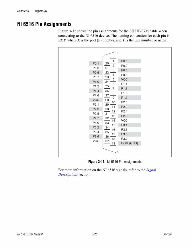
NI 6516 Pin AssignmentsFigure 3-12 shows the pin assignments for the SH37F-37M cable when connecting to the NI 6516 device. The naming convention for each pin is PX.Y, where X is the port (P) number, and Y is the line number or name.
Figure 3-12. NI 6516 Pin Assignments
For more information on the NI 6516 signals, refer to the Signal Descriptions section.
1
2
3
4
5
6
7
8
9
10
11
12
13
14
15
16
17
18
19
20
21
22
23
24
25
26
27
28
29
30
31
32
33
34
35
36
37
P0.0
P0.2
P0.4
P0.6
VCC
P1.1
P1.3
P1.5
P1.7
P2.0
P2.2
P2.4
P2.6
VCC
P3.1
P3.3
P3.5
P3.7
COM (GND)
P0.1
P0.3
P0.5
P0.7
P1.0
P1.2
P1.4
P1.6
VCC
P2.1
P2.3
P2.5
P2.7
P3.0
P3.2
P3.4
P3.6
VCC
Chapter 3 Digital I/O
© National Instruments Corporation 3-21 NI 651x User Manual
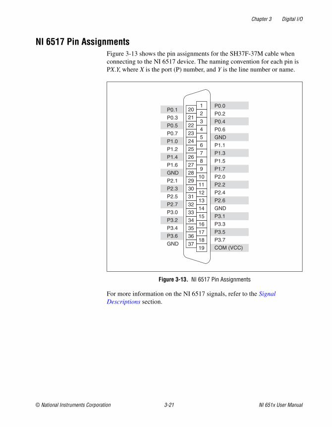
NI 6517 Pin AssignmentsFigure 3-13 shows the pin assignments for the SH37F-37M cable when connecting to the NI 6517 device. The naming convention for each pin is PX.Y, where X is the port (P) number, and Y is the line number or name.
Figure 3-13. NI 6517 Pin Assignments
For more information on the NI 6517 signals, refer to the Signal Descriptions section.
1
2
3
4
5
6
7
8
9
10
11
12
13
14
15
16
17
18
19
20
21
22
23
24
25
26
27
28
29
30
31
32
33
34
35
36
37
P0.0
P0.2
P0.4
P0.6
GND
P1.1
P1.3
P1.5
P1.7
P2.0
P2.2
P2.4
P2.6
GND
P3.1
P3.3
P3.5
P3.7
COM (VCC)
P0.1
P0.3
P0.5
P0.7
P1.0
P1.2
P1.4
P1.6
GND
P2.1
P2.3
P2.5
P2.7
P3.0
P3.2
P3.4
P3.6
GND

Chapter 3 Digital I/O
NI 651x User Manual 3-22 ni.com
NI 6518 Pin AssignmentsFigure 3-14 shows the pin assignments for the SH37F-37M cable when connecting to the NI 6518 device. The naming convention for each pin is PX.Y, where X is the port (P) number, and Y is the line number or name.
Figure 3-14. NI 6518 Pin Assignments
For more information on the NI 6518 signals, refer to the Signal Descriptions section.
1
2
3
4
5
6
7
8
9
10
11
12
13
14
15
16
17
18
19
20
21
22
23
24
25
26
27
28
29
30
31
32
33
34
35
36
37
P0.0
P0.2
P0.4
P0.6
P1.0
P1.2
P1.4
P1.6
IN.COM
VCC
P2.0
P2.2
P2.4
P2.6
P3.0
P3.2
P3.4
P3.6
OUT.COM (GND)
P0.1
P0.3
P0.5
P0.7
P1.1
P1.3
P1.5
P1.7
VCC
VCC
P2.1
P2.3
P2.5
P2.7
P3.1
P3.3
P3.5
P3.7

Chapter 3 Digital I/O
© National Instruments Corporation 3-23 NI 651x User Manual
NI 6519 Pin AssignmentsFigure 3-15 shows the pin assignments for the SH37F-37M cable when connecting to the NI 6519 device. The naming convention for each pin is PX.Y, where X is the port (P) number, and Y is the line number or name.
Figure 3-15. NI 6519 Pin Assignments
For more information on the NI 6519 signals, refer to the Signal Descriptions section.
1
2
3
4
5
6
7
8
9
10
11
12
13
14
15
16
17
18
19
20
21
22
23
24
25
26
27
28
29
30
31
32
33
34
35
36
37
P0.0
P0.2
P0.4
P0.6
P1.0
P1.2
P1.4
P1.6
IN.COM
GND
P2.0
P2.2
P2.4
P2.6
P3.0
P3.2
P3.4
P3.6
OUT.COM (VCC)
P0.1
P0.3
P0.5
P0.7
P1.1
P1.3
P1.5
P1.7
GND
GND
P2.1
P2.3
P2.5
P2.7
P3.1
P3.3
P3.5
P3.7
Chapter 3 Digital I/O
NI 651x User Manual 3-24 ni.com
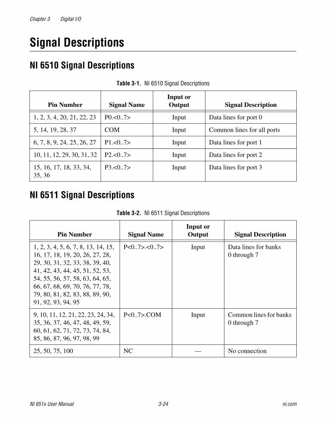
Signal Descriptions
NI 6510 Signal Descriptions
NI 6511 Signal Descriptions
Table 3-1. NI 6510 Signal Descriptions
Pin Number Signal NameInput or Output Signal Description
1, 2, 3, 4, 20, 21, 22, 23 P0.<0..7> Input Data lines for port 0
5, 14, 19, 28, 37 COM Input Common lines for all ports
6, 7, 8, 9, 24, 25, 26, 27 P1.<0..7> Input Data lines for port 1
10, 11, 12, 29, 30, 31, 32 P2.<0..7> Input Data lines for port 2
15, 16, 17, 18, 33, 34, 35, 36
P3.<0..7> Input Data lines for port 3
Table 3-2. NI 6511 Signal Descriptions
Pin Number Signal NameInput or Output Signal Description
1, 2, 3, 4, 5, 6, 7, 8, 13, 14, 15, 16, 17, 18, 19, 20, 26, 27, 28, 29, 30, 31, 32, 33, 38, 39, 40, 41, 42, 43, 44, 45, 51, 52, 53, 54, 55, 56, 57, 58, 63, 64, 65, 66, 67, 68, 69, 70, 76, 77, 78, 79, 80, 81, 82, 83, 88, 89, 90, 91, 92, 93, 94, 95
P<0..7>.<0..7> Input Data lines for banks 0 through 7
9, 10, 11, 12, 21, 22, 23, 24, 34, 35, 36, 37, 46, 47, 48, 49, 59, 60, 61, 62, 71, 72, 73, 74, 84, 85, 86, 87, 96, 97, 98, 99
P<0..7>.COM Input Common lines for banks 0 through 7
25, 50, 75, 100 NC — No connection

Chapter 3 Digital I/O
© National Instruments Corporation 3-25 NI 651x User Manual
NI 6512 Signal Descriptions
NI 6513 Signal Descriptions
Table 3-3. NI 6512 Signal Descriptions
Pin Number Signal NameInput or Output Signal Description
1, 2, 3, 4, 5, 6, 7, 8, 13, 14, 15, 16, 17, 18, 19, 20, 26, 27, 28, 29, 30, 31, 32, 33, 38, 39, 40, 41, 42, 43, 44, 45, 51, 52, 53, 54, 55, 56, 57, 58, 63, 64, 65, 66, 67, 68, 69, 70, 76, 77, 78, 79, 80, 81, 82, 83, 88, 89, 90, 91, 92, 93, 94, 95
P<0..7>.<0..7> Output Data lines for banks 0 through 7
9, 21, 34, 46, 59, 71, 84, 96 P<0..7>.COM (GND) Input Ground for banks 0 through 7;isolated to the computer ground signal
10, 11, 12, 22, 23, 24, 35, 36, 37, 47, 48, 49, 60, 61, 62, 72, 73, 74, 85, 86, 87, 97, 98, 99
P<0..7>.VCC Input Power lines for banks 0 through 7
25, 75 NC — No connection
50, 100 P<6..7>.+5V Output +5 V for banks 6 and 7
Table 3-4. NI 6513 Signal Descriptions
Pin Number Signal NameInput or Output Signal Description
1, 2, 3, 4, 5, 6, 7, 8, 13, 14, 15, 16, 17, 18, 19, 20, 26, 27, 28, 29, 30, 31, 32, 33, 38, 39, 40, 41, 42, 43, 44, 45, 51, 52, 53, 54, 55, 56, 57, 58, 63, 64, 65, 66, 67, 68, 69, 70, 76, 77, 78, 79, 80, 81, 82, 83, 88, 89, 90, 91, 92, 93, 94, 95
P<0..7>.<0..7> Output Data lines for banks 0 through 7
9, 21, 34, 46, 59, 71, 84, 96 P<0..7>.COM (VCC) Input Power lines for banks 0 through 7

Chapter 3 Digital I/O
NI 651x User Manual 3-26 ni.com
NI 6514 Signal Descriptions
10, 11, 12, 22, 23, 24, 35, 36, 37, 47, 48, 49, 60, 61, 62, 72, 73, 74, 85, 86, 87, 97, 98, 99
P<0..7>.GND Input Ground for banks 0 through 7; isolated to the computer ground signal
25, 75 NC — No connection
50, 100 P<6..7>.+5V Output +5 V for banks 6 and 7
Table 3-5. NI 6514 Signal Descriptions
Pin Number Signal NameInput or Output Signal Description
1, 2, 3, 4, 5, 6, 7, 8 P0.<0..7> Input Data lines for bank 0
9, 10, 11, 12 P0.COM Input Common lines for bank 0
51, 52, 53, 54, 55, 56, 57, 58 P1.<0..7> Input Data lines for bank 1
59, 60, 61, 62 P1.COM Input Common lines for bank 1
13, 14, 15, 16, 17, 18, 19, 20 P2.<0..7> Input Data lines for bank 2
21, 22, 23, 24 P2.COM Input Common lines for bank 2
63, 64, 65, 66, 67, 68, 69, 70 P3.<0..7> Input Data lines for bank 3
71, 72, 73, 74 P3.COM Input Common lines for bank 3
25, 75 NC — No connection
26, 27, 28, 29, 30, 31, 32, 33 P4.<0..7> Output Data lines for bank 4
34 P4.COM (GND) Input Ground for bank 4; isolated to the computer ground signal
35, 36, 37 P4.VCC Input Power lines for bank 4
76, 77, 78,79, 80, 81, 82, 83 P5.<0..7> Output Data lines for bank 5
Table 3-4. NI 6513 Signal Descriptions (Continued)
Pin Number Signal NameInput or Output Signal Description
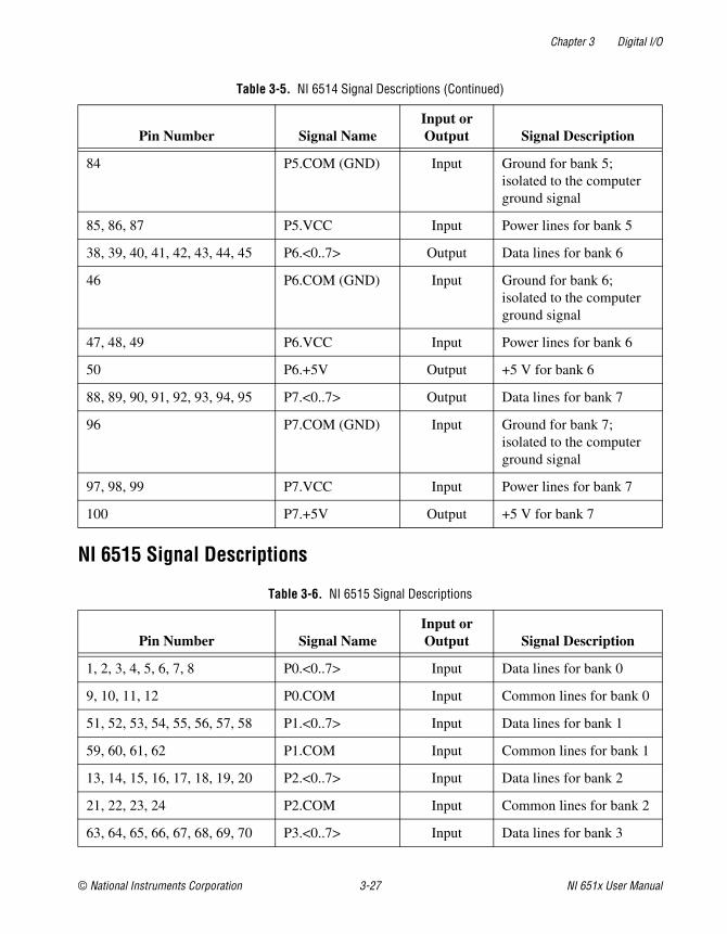
Chapter 3 Digital I/O
© National Instruments Corporation 3-27 NI 651x User Manual
NI 6515 Signal Descriptions
84 P5.COM (GND) Input Ground for bank 5; isolated to the computer ground signal
85, 86, 87 P5.VCC Input Power lines for bank 5
38, 39, 40, 41, 42, 43, 44, 45 P6.<0..7> Output Data lines for bank 6
46 P6.COM (GND) Input Ground for bank 6; isolated to the computer ground signal
47, 48, 49 P6.VCC Input Power lines for bank 6
50 P6.+5V Output +5 V for bank 6
88, 89, 90, 91, 92, 93, 94, 95 P7.<0..7> Output Data lines for bank 7
96 P7.COM (GND) Input Ground for bank 7; isolated to the computer ground signal
97, 98, 99 P7.VCC Input Power lines for bank 7
100 P7.+5V Output +5 V for bank 7
Table 3-6. NI 6515 Signal Descriptions
Pin Number Signal NameInput or Output Signal Description
1, 2, 3, 4, 5, 6, 7, 8 P0.<0..7> Input Data lines for bank 0
9, 10, 11, 12 P0.COM Input Common lines for bank 0
51, 52, 53, 54, 55, 56, 57, 58 P1.<0..7> Input Data lines for bank 1
59, 60, 61, 62 P1.COM Input Common lines for bank 1
13, 14, 15, 16, 17, 18, 19, 20 P2.<0..7> Input Data lines for bank 2
21, 22, 23, 24 P2.COM Input Common lines for bank 2
63, 64, 65, 66, 67, 68, 69, 70 P3.<0..7> Input Data lines for bank 3
Table 3-5. NI 6514 Signal Descriptions (Continued)
Pin Number Signal NameInput or Output Signal Description
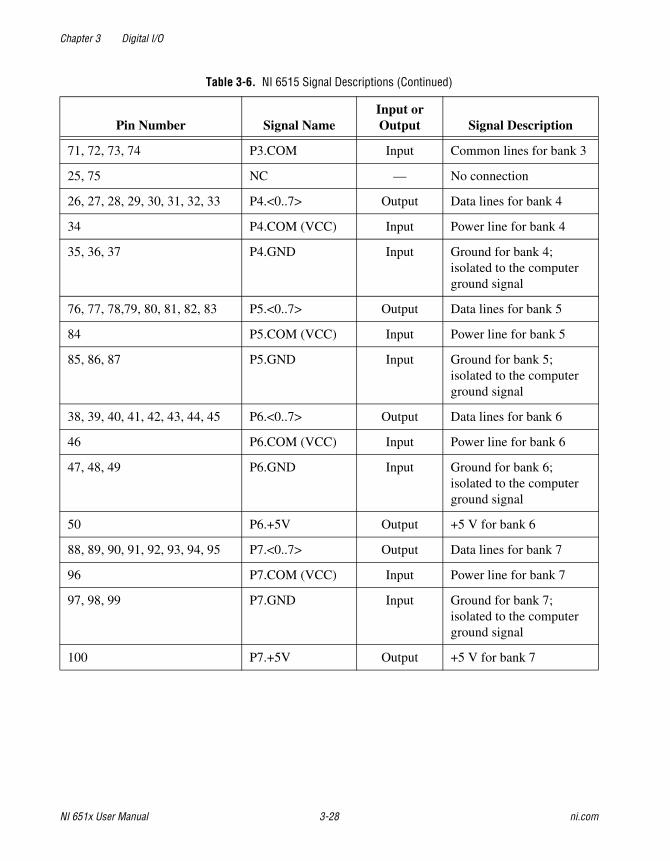
Chapter 3 Digital I/O
NI 651x User Manual 3-28 ni.com
71, 72, 73, 74 P3.COM Input Common lines for bank 3
25, 75 NC — No connection
26, 27, 28, 29, 30, 31, 32, 33 P4.<0..7> Output Data lines for bank 4
34 P4.COM (VCC) Input Power line for bank 4
35, 36, 37 P4.GND Input Ground for bank 4; isolated to the computer ground signal
76, 77, 78,79, 80, 81, 82, 83 P5.<0..7> Output Data lines for bank 5
84 P5.COM (VCC) Input Power line for bank 5
85, 86, 87 P5.GND Input Ground for bank 5; isolated to the computer ground signal
38, 39, 40, 41, 42, 43, 44, 45 P6.<0..7> Output Data lines for bank 6
46 P6.COM (VCC) Input Power line for bank 6
47, 48, 49 P6.GND Input Ground for bank 6; isolated to the computer ground signal
50 P6.+5V Output +5 V for bank 6
88, 89, 90, 91, 92, 93, 94, 95 P7.<0..7> Output Data lines for bank 7
96 P7.COM (VCC) Input Power line for bank 7
97, 98, 99 P7.GND Input Ground for bank 7; isolated to the computer ground signal
100 P7.+5V Output +5 V for bank 7
Table 3-6. NI 6515 Signal Descriptions (Continued)
Pin Number Signal NameInput or Output Signal Description
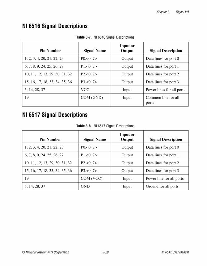
Chapter 3 Digital I/O
© National Instruments Corporation 3-29 NI 651x User Manual
NI 6516 Signal Descriptions
NI 6517 Signal Descriptions
Table 3-7. NI 6516 Signal Descriptions
Pin Number Signal NameInput or Output Signal Description
1, 2, 3, 4, 20, 21, 22, 23 P0.<0..7> Output Data lines for port 0
6, 7, 8, 9, 24, 25, 26, 27 P1.<0..7> Output Data lines for port 1
10, 11, 12, 13, 29, 30, 31, 32 P2.<0..7> Output Data lines for port 2
15, 16, 17, 18, 33, 34, 35, 36 P3.<0..7> Output Data lines for port 3
5, 14, 28, 37 VCC Input Power lines for all ports
19 COM (GND) Input Common line for all ports
Table 3-8. NI 6517 Signal Descriptions
Pin Number Signal NameInput or Output Signal Description
1, 2, 3, 4, 20, 21, 22, 23 P0.<0..7> Output Data lines for port 0
6, 7, 8, 9, 24, 25, 26, 27 P1.<0..7> Output Data lines for port 1
10, 11, 12, 13, 29, 30, 31, 32 P2.<0..7> Output Data lines for port 2
15, 16, 17, 18, 33, 34, 35, 36 P3.<0..7> Output Data lines for port 3
19 COM (VCC) Input Power line for all ports
5, 14, 28, 37 GND Input Ground for all ports

Chapter 3 Digital I/O
NI 651x User Manual 3-30 ni.com
NI 6518 Signal Descriptions
NI 6519 Signal Descriptions
Table 3-9. NI 6518 Signal Descriptions
Pin Number Signal NameInput or Output* Signal Description
1, 2, 3, 4, 20, 21, 22, 23 P0.<0..7> Input Data lines for port 0
5, 6, 7, 8, 24, 25, 26, 27 P1.<0..7> Input Data lines for port 1
11, 12, 13, 14, 30, 31, 32, 33 P2.<0..7> Output Data lines for port 2
15, 16, 17, 18, 34, 35, 36, 37 P3.<0..7> Output Data lines for port 3
9 IN.COM Input Common line for all input channels
10, 28, 29 VCC Input Power lines for all ports
19 OUT.COM (GND) Input Ground for all output channels
* The NI 6518 inputs are isolated from the outputs.
Table 3-10. NI 6519 Signal Descriptions
Pin Number Signal NameInput or Output* Signal Description
1, 2, 3, 4, 20, 21, 22, 23 P0.<0..7> Input Data lines for port 0
5, 6, 7, 8, 24, 25, 26, 27 P1.<0..7> Input Data lines for port 1
11, 12, 13, 14, 30, 31, 32, 33 P2.<0..7> Output Data lines for port 2
15, 16, 17, 18, 34, 35, 36, 37 P3.<0..7> Output Data lines for port 3
9 IN.COM Input Common line for all input channels
10, 28, 29 GND Input Ground for all ports
19 OUT.COM (VCC) Input Power line for all output channels
* The NI 6519 inputs are isolated from the outputs.
© National Instruments Corporation 4-1 NI 651x User Manual
4Power Connections
Isolation
NI 6510The NI 6510 has 32 channels that consist of four eight-line ports. All channels belong to one isolated bank and use the same common. The NI 6510 digital inputs are isolated from the computer power supply. Isolated photocouplers provide isolation.
NI 6511The inputs in each bank of the NI 6511 device are isolated from the inputs in other banks, from PX.COM pins in other banks, and from the computer power supply. All lines in the same input bank use the same common. Isolated photocouplers provide isolation.
NI 6512/6513The outputs in each bank of the NI 6512/6513 device are isolated from the outputs in other banks, from the +5 V and PX.GND pins in other banks, and from the computer power supply. All lines in the same output bank use the same common power and ground. Isolated photocouplers provide isolation.
NI 6514/6515The inputs and outputs in each bank of the NI 6514/6515 are isolated from the inputs and outputs in other banks, from the +5 V and PX.GND pins in other banks, and from the computer power supply. All lines in the same input or output bank use the same common power and ground. Isolated photocouplers provide isolation.
NI 6516/6517The NI 6516/6517 has 32 channels that consist of four eight-line ports. All channels belong to one isolated bank and use the same common. The NI 6516/6517 digital outputs are isolated from the computer power supply. Isolated photocouplers provide isolation.

Chapter 4 Power Connections
NI 651x User Manual 4-2 ni.com
NI 6518/6519The NI 6518/6519 has 32 channels that consist of four eight-line ports. Ports 0 and 1 (inputs) belong to the same bank, and Ports 2 and 3 (outputs) belong to the same bank, and inputs are isolated from outputs. Each bank shares the same common. The NI 6518/6519 digital inputs and outputs are isolated from the computer power supply and from one another. Isolated photocouplers provide isolation.
Optically Isolated Inputs (NI 6510/6511/6514/6515/6518/6519)
The input lines provide 32 lines of optically isolated digital input on the NI 6510/6514/6515 device, 64 lines of optically isolated digital input on the NI 6511 device, and 16 lines of optically isolated digital input on the NI 6518/6519 device. These inputs contain an AC input photocoupler and a resistor for current limiting. The maximum input voltage (VIN) on these lines is 30 VDC.
Sensing DC Voltages(NI 6510/6511/6514/6515/6518/6519 Only) These devices can sense DC signals from 11 V to DC power supply levels up to 30 V.
Applying a DC voltage of at least 11 V across the two input terminals registers a logic high for that input. If no voltage is present (a voltage of 4 V or less), the device registers a logic low for that input. DC voltages between 4 V and 11 V are invalid and register an unreliable value.
Input Signal Connection Example(NI 6510/6511/6514/6515/6518/6519 Only) The following figures show signal connections for a supply connected to an isolated input on these devices. The power supply can be any DC voltage within the device range. Refer to the NI 651x Specifications, available at ni.com/manuals, for information about voltage ranges.

Chapter 4 Power Connections
© National Instruments Corporation 4-3 NI 651x User Manual
Figure 4-1. NI 6510 Signal Connection Example
Figure 4-2. NI 6511 Input Signal Connection Example
AC InputPhotocoupler
+3.3 V
P<0..3>.<0..7>
COM
NI 6510
0 V ~ +30 Vor
0 V ~ –30 V
AC InputPhotocoupler
+3.3 V
P<0..7>.<0..7>
P<0..7>.COM
NI 6511
0 V ~ +30 Vor
0 V ~ –30 V
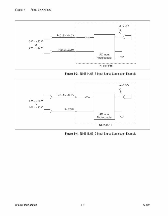
Chapter 4 Power Connections
NI 651x User Manual 4-4 ni.com
Figure 4-3. NI 6514/6515 Input Signal Connection Example
Figure 4-4. NI 6518/6519 Input Signal Connection Example
AC InputPhotocoupler
+3.3 V
P<0..3>.<0..7>
P<0..3>.COM
NI 6514/15
0 V ~ +30 Vor
0 V ~ –30 V
AC InputPhotocoupler
+3.3 V
P<0..1>.<0..7>
IN.COM
NI 6518/19
0 V ~ +30 Vor
0 V ~ –30 V

Chapter 4 Power Connections
© National Instruments Corporation 4-5 NI 651x User Manual
Optically Isolated Outputs with Darlington Arrays (NI 6512/6513/6514/6515/6516/6517/6518/6519)
The outputs on the NI 6512/6513/6514/6515/6516/6517/6518/6519 device are optically isolated photocouplers with Darlington arrays. You can configure the outputs as follows:
• Writing a 1 (logic high) to an output line switches on one channel of the Darlington array and allows current to pass through the output line.
• Writing a 0 (logic low) to an output line switches off one channel of the Darlington array and prohibits current from passing through the output line.
• (NI 6512/6513/6514/6515 Only) To supply +5 V of isolated power, use an external power supply over +8 V on Bank 6 and Bank 7.
Note The maximum external voltage on these lines is 30 VDC.
Caution Do not reverse the external voltage polarity or exceed the maximum output specifications. Doing so could permanently damage the NI 6512/6513/6514/6515/6516/6517/6518/6519 device and the power supply if it is not protected.
Power-On and Power-Off Conditions(NI 6512/6513/6514/6515/6516/6517/6518/6519 Only) At power-on and power-off, the Darlington arrays on these devices switch off.
Output Signal Connection Example (Sourcing Current)The following figures show examples of driving a load with the photocouplers and Darlington arrays (sourcing current).

Chapter 4 Power Connections
NI 651x User Manual 4-6 ni.com
Figure 4-5. NI 6512 Output Signal Connection Example
Figure 4-6. NI 6514 Output Signal Connection Example
VoltageRegulator
P<0..7>.COM (GND)
P<0..7>.<0..7>
+–DC
LOAD
+5 V ~ +30 V
OutputPhotocoupler
+3.3 V
P<0..7>.VCC
NI 6512
DarlingtonDriver
VoltageRegulator
P<4..7>.COM (GND)
P<4..7>.<0..7>
+–DC
LOAD
+5 V ~ +30 V
OutputPhotocoupler
+3.3 V
P<4..7>.VCC
NI 6514
DarlingtonDriver
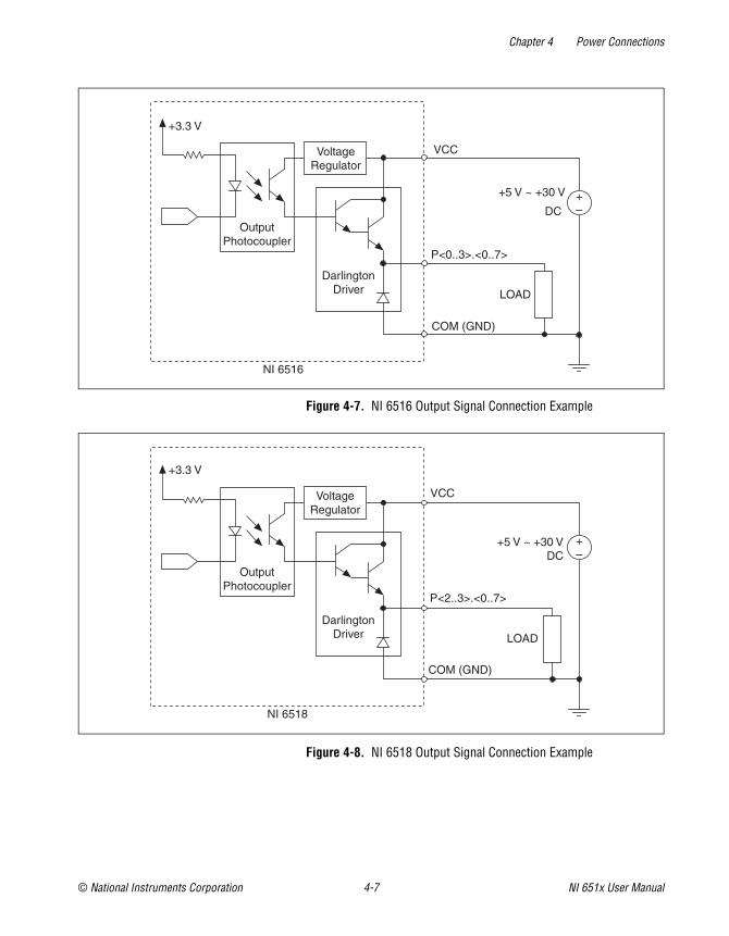
Chapter 4 Power Connections
© National Instruments Corporation 4-7 NI 651x User Manual
Figure 4-7. NI 6516 Output Signal Connection Example
Figure 4-8. NI 6518 Output Signal Connection Example
VoltageRegulator
COM (GND)
P<0..3>.<0..7>
+–DC
LOAD
+5 V ~ +30 V
OutputPhotocoupler
+3.3 V
VCC
NI 6516
DarlingtonDriver
VoltageRegulator
COM (GND)
P<2..3>.<0..7>
+–
LOAD
+5 V ~ +30 VDC
OutputPhotocoupler
+3.3 V
VCC
NI 6518
DarlingtonDriver

Chapter 4 Power Connections
NI 651x User Manual 4-8 ni.com
Distributing Current (NI 6516/6518 Only)In applications that drive many high-current loads, a large amount of current must be returned on the VCC pins. When connecting the NI 6516/6518 to multiple loads, physically connect to all VCC pins on the device, as shown in Figure 4-9 and Figure 4-10. Connecting to all VCC pins distributes the current evenly among the VCC pins and lowers the amount of current driven on any single cable wire and on the accessory terminals.
Figure 4-9. NI 6516 GND Connection Example
RL0 . . .
P0.0
P0.1
P0.2
P3.7
VCC, Pin 5
VCC, Pin14
VCC, Pin 28
VCC, Pin 37
COM
+–
+5 V ~ +30 V

Chapter 4 Power Connections
© National Instruments Corporation 4-9 NI 651x User Manual
Figure 4-10. NI 6518 GND Connection Example
Refer to the NI SH37F-37M Cable section of Chapter 5, Cables and Accessories, for more information.
Output Signal Connection Example (Sinking Current)The following figures show examples of driving a load with the photocouplers and Darlington arrays (sinking current).
Caution Make sure that P<0..7>.COM (VCC) is connected to the positive pole of the power supply and that P<0..7>.GND is connected to the negative pole of the power supply. Failure to do so could permanently damage the NI 6513 device and the power supply if it is not protected.
RL0 . . .
P0.0
P0.1
P0.2
P3.7
VCC, Pin10
VCC, Pin 28
VCC, Pin 29
COM
+–
+5 V ~ +30 V
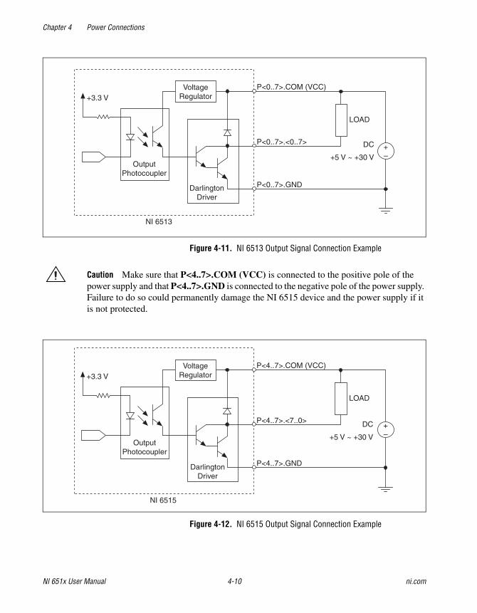
Chapter 4 Power Connections
NI 651x User Manual 4-10 ni.com
Figure 4-11. NI 6513 Output Signal Connection Example
Caution Make sure that P<4..7>.COM (VCC) is connected to the positive pole of the power supply and that P<4..7>.GND is connected to the negative pole of the power supply. Failure to do so could permanently damage the NI 6515 device and the power supply if it is not protected.
Figure 4-12. NI 6515 Output Signal Connection Example
VoltageRegulator
P<0..7>.COM (VCC)
P<0..7>.<0..7>
P<0..7>.GND
+–
DC
LOAD
+5 V ~ +30 VOutput
Photocoupler
+3.3 V
NI 6513
DarlingtonDriver
VoltageRegulator
P<4..7>.COM (VCC)
P<4..7>.<7..0>
P<4..7>.GND
+–
DC
LOAD
+5 V ~ +30 VOutput
Photocoupler
+3.3 V
NI 6515
DarlingtonDriver

Chapter 4 Power Connections
© National Instruments Corporation 4-11 NI 651x User Manual
Caution Make sure that COM (VCC) is connected to the positive pole of the power supply and that GND is connected to the negative pole of the power supply. Failure to do so could permanently damage the NI 6517 device and the power supply if it is not protected.
Figure 4-13. NI 6517 Output Signal Connection Example
VoltageRegulator
COM (VCC)
P<0..3>.<0..7>
GND
+–
DC
LOAD
+5 V ~ +30 VOutput
Photocoupler
+3.3 V
NI 6517
DarlingtonDriver

Chapter 4 Power Connections
NI 651x User Manual 4-12 ni.com
Caution Make sure that OUT.COM (VCC) is connected to the positive pole of the power supply and that GND is connected to the negative pole of the power supply. Failure to do so could permanently damage the NI 6519 device and the power supply if it is not protected.
Figure 4-14. NI 6519 Output Signal Connection Example
Distributing Current (NI 6517/6519 Only)In applications that drive many high-current loads, a large amount of current must be returned on the GND pins. When connecting the NI 6517/6519 to multiple loads, physically connect to all GND pins on the device, as shown in Figure 4-15 and Figure 4-16. Connecting to all GND pins distributes the current evenly among the GND pins and lowers the amount of current driven on any single cable wire and on the accessory terminals.
VoltageRegulator
OUT.COM (VCC)
P<2..3>.<0..7>
GND
+–
DC
LOAD
+5 V ~ +30 VOutput
Photocoupler
+3.3 V
NI 6519
DarlingtonDriver
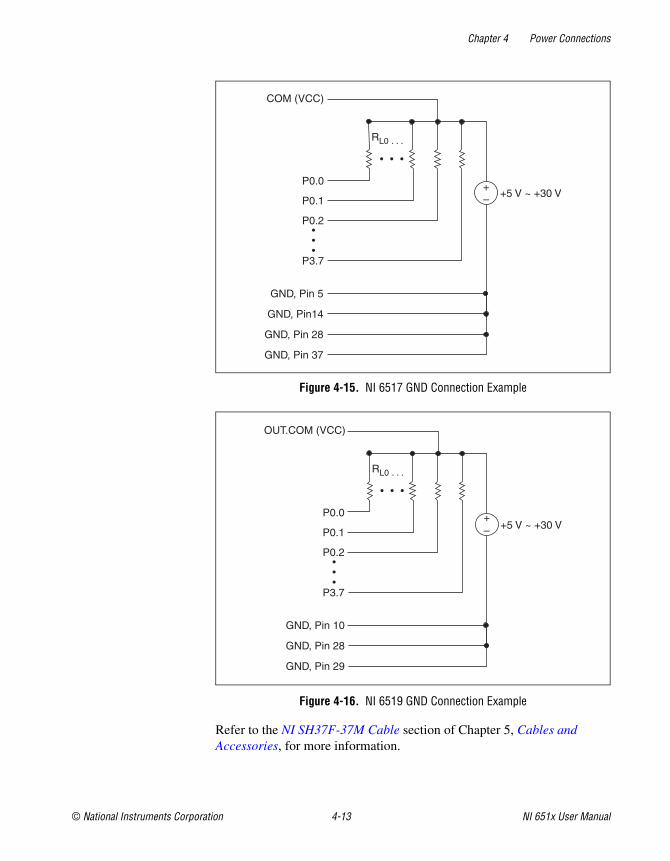
Chapter 4 Power Connections
© National Instruments Corporation 4-13 NI 651x User Manual
Figure 4-15. NI 6517 GND Connection Example
Figure 4-16. NI 6519 GND Connection Example
Refer to the NI SH37F-37M Cable section of Chapter 5, Cables and Accessories, for more information.
RL0 . . .
P0.0
P0.1
P0.2
P3.7
GND, Pin 5
GND, Pin14
GND, Pin 28
GND, Pin 37
COM (VCC)
+– +5 V ~ +30 V
RL0 . . .
P0.0
P0.1
P0.2
P3.7
GND, Pin 10
GND, Pin 28
GND, Pin 29
OUT.COM (VCC)
+5 V ~ +30 V–+

© National Instruments Corporation 5-1 NI 651x User Manual
5Cables and Accessories
National Instruments offers the following products for use with NI 651x devices.
Accessories for 37-Pin DevicesNational Instruments offers the following connectivity options for use with 37-pin safety low voltage (≤60 VDC/42.4 Vpk/30 Vrms) NI 6510/6516/6517/6518/6519 devices.
Choose from the following screw terminal connectivity options:
• CB-37F Connector Block—part number 778672-01 (vertical) and 778673-01 (horizontal)
• CB-37F-LP Unshielded, I/O Connector Block with 37-Pin D-SUB—part number 779353-01
With one of the following cabling options:
– SH37F-37M Shielded Cable—part number 778621-01 (1 m) and 778621-02 (2 m)
– SH37F-P-4 37-Pin Female-to-Pigtails Shielded I/O Cable—part number 778620-04 (4 m)
– R37F-37M-1 37-Pin Female-to-Male Ribbon I/O Cable—part number 779195-01 (1 m)
You may also choose from the following custom connectivity options:
• SH37F-P-4 37-Pin Female-to-Pigtails Shielded I/O Cable—part number 778620-04 (4 m)
• TB-37F-37CP 37-Pin Crimp & Poke Terminals, Shell with Strain Relief—part number 779185-01
• TB-37F-37SC 37-Pin Solder Cup Terminals, Shell with Strain Relief—part number 779184-01
For more information about optional equipment available from National Instruments, refer to the National Instruments catalog or visit the National Instruments Web site at ni.com.

Chapter 5 Cables and Accessories
NI 651x User Manual 5-2 ni.com
NI SH37F-37M CableThe NI SH37F-37M cable is a 37-pin shielded cable that provides direct connection to 37-pin 651x devices. This cable uses 26 AWG wire that has a maximum current rating of 1.2 A per line. Some devices that can be physically connected to this cable have current ratings that exceed this limitation. The NI SH37F-37M cable is not intended for use with hazardous voltages (greater than 60 VDC, 42.4 V peak, or 30 Vrms).
Ensure that the DIO device does not exceed the maximum current rating by evenly distributing the current among the VCC pins on the NI 6516 and NI 6518 devices, or among the GND pins on the NI 6517 and NI 6519 devices. For more information, refer to the Distributing Current (NI 6516/6518 Only) section and Distributing Current (NI 6517/6519 Only) section of Chapter 4, Power Connections.
For quick connection to the I/O connector, use the National Instruments CB-37F terminal block with the NI SH37F-37M cable.
Accessories for 100-Pin DevicesNational Instruments offers the following products for use with NI 6511/6512/6513/6514/6515 devices.
For more information about optional equipment available from National Instruments, refer to the National Instruments catalog or visit the National Instruments Web site at ni.com.
SH100-100-F CableThe SH100-100-F cable is a 100-pin shielded cable that provides direct connection to 100-pin devices. For quick connection to the I/O connector, use the National Instruments SCB-100 terminal block with the SH100-100-F cable.
Cable (Part Number) Accessory (Part Number)
SH100-100-F shielded cable (185095) SCB-100 connector block (776990)
R1005050 ribbon cable (182762) CB-50 connector block, DIN-rail mount (776164)
CB-50LP connector block, panel mount (777101)
Chapter 5 Cables and Accessories
© National Instruments Corporation 5-3 NI 651x User Manual
R1005050 Ribbon CableThe 100-pin R1005050 ribbon cable splits into two 50-pin cables for direct connection to one or two 50-pin accessories. The 100-pin connector that joins the two cables plugs into the I/O connector on the DIO device.
For quick connection to the I/O connector, use the CB-50 or CB-50LP terminal blocks with the R1005050 cable.

© National Instruments Corporation A-1 NI 651x User Manual
ATechnical Support and Professional Services
Visit the following sections of the award-winning National Instruments Web site at ni.com for technical support and professional services:
• Support—Technical support at ni.com/support includes the following resources:
– Self-Help Technical Resources—For answers and solutions, visit ni.com/support for software drivers and updates, a searchable KnowledgeBase, product manuals, step-by-step troubleshooting wizards, thousands of example programs, tutorials, application notes, instrument drivers, and so on. Registered users also receive access to the NI Discussion Forums at ni.com/forums. NI Applications Engineers make sure every question submitted online receives an answer.
– Standard Service Program Membership—This program entitles members to direct access to NI Applications Engineers via phone and email for one-to-one technical support as well as exclusive access to on demand training modules via the Services Resource Center. NI offers complementary membership for a full year after purchase, after which you may renew to continue your benefits.
For information about other technical support options in your area, visit ni.com/services, or contact your local office at ni.com/contact.
• Training and Certification—Visit ni.com/training for self-paced training, eLearning virtual classrooms, interactive CDs, and Certification program information. You also can register for instructor-led, hands-on courses at locations around the world.
• System Integration—If you have time constraints, limited in-house technical resources, or other project challenges, National Instruments Alliance Partner members can help. To learn more, call your local NI office or visit ni.com/alliance.

Appendix A Technical Support and Professional Services
NI 651x User Manual A-2 ni.com
• Declaration of Conformity (DoC)—A DoC is our claim of compliance with the Council of the European Communities using the manufacturer’s declaration of conformity. This system affords the user protection for electromagnetic compatibility (EMC) and product safety. You can obtain the DoC for your product by visiting ni.com/certification.
• Calibration Certificate—If your product supports calibration, you can obtain the calibration certificate for your product at ni.com/calibration.
If you searched ni.com and could not find the answers you need, contact your local office or NI corporate headquarters. Phone numbers for our worldwide offices are listed at the front of this manual. You also can visit the Worldwide Offices section of ni.com/niglobal to access the branch office Web sites, which provide up-to-date contact information, support phone numbers, email addresses, and current events.
© National Instruments Corporation G-1 NI 651x User Manual
Glossary
Symbol Prefix Value
n nano 10–9
μ micro 10–6
m milli 10–3
k kilo 103
A
A amperes
ASIC Application Specific Integrated Circuit
C
C Celsius
D
DI digital input
DMA direct memory access—A method by which data can be transferred to/from computer memory from/to a device or memory on the bus while the processor does something else. DMA is the fastest method of transferring data to/from computer memory.
DO digital output

Glossary
NI 651x User Manual G-2 ni.com
F
Form A relay a single-pole single-throw (SPST) relay with a default state of normally open
Form C relay a single-pole double-throw (SPDT) relay that breaks the connection with one throw before making contact with the other (break-before-make)
G
GND ground signal
H
hex hexadecimal
I
inductive load A reactive load in which the inductive reactance exceeds the capacitive reactance and therefore carries a lagging current with respect to the voltage across the terminals.
L
latching the ability to keep a relay contact in its current state if power is removed
logic A sequence of functions made up of circuits designed to perform an operation.
LSB least significant bit
M
MSB most significant bit

Glossary
© National Instruments Corporation G-3 NI 651x User Manual
N
non-latching relay A type of electromechanical relay that has an initial position of normally closed (NC). This position is maintained by the force of a spring or permanent magnet while no current flows. The normally open (NO) contact is maintained by the force of a magnetic field while current flows through the coil. When the current stops, the relay reverts back to its initial NC position.
P
PCI Peripheral Component Interconnect—A high-performance expansion bus architecture originally developed by Intel to replace ISA and EISA. It is achieving widespread acceptance as a standard for PCs and workstations; it offers a theoretical maximum transfer rate of 132 Mbytes/s.
port A digital port, consisting of four or eight lines of digital input and/or output.
S
S samples
s seconds
SCSI Small Computer System Interface. Interface for communication between devices.
signal conditioning The manipulation of signals to prepare them for digitizing.
T
TTL transistor-transistor logic
V
VCC Supply voltage; for example, the voltage a computer supplies to its plug-in devices.
VDC volts direct current
Glossary
NI 651x User Manual G-4 ni.com
VI virtual instrument—A combination of hardware and/or software elements, typically used with a PC, that has the functionality of a classic standalone instrument.
VI input voltage
W
W watts

© National Instruments Corporation I-1 NI 651x User Manual
Index
Aaccessories
for 100-pin devices, 5-2for 37-pin devices, 5-1
Bblock diagrams. See functional overview
Ccalibration certificate (NI resources), A-2change detection, 2-3
example, 2-4components. See functional overviewconfiguration, 1-2conventions used in the manual, ix
DDeclaration of Conformity (NI resources), A-2diagnostic tools (NI resources), A-1digital filtering, 2-1
example, 2-2digital I/O
NI 6510, 3-1NI 6511, 3-1NI 6512/6513, 3-2NI 6514/6515, 3-3NI 6516/6517, 3-3NI 6518/6519, 3-4
distributing currentNI 6516, 4-8NI 6517, 4-12NI 6518, 4-8NI 6519, 4-12
documentationconventions used in manual, ixNI resources, A-1
drivers (NI resources), A-1
Eexamples (NI resources), A-1
Ffunctional overview
NI 6510 (figure), 1-3NI 6511 (figure), 1-3NI 6512 (figure), 1-4NI 6513 (figure), 1-4NI 6514 (figure), 1-5NI 6515 (figure), 1-5NI 6516 (figure), 1-6NI 6517 (figure), 1-6NI 6518 (figure), 1-7NI 6519 (figure), 1-7
fundamentalsNI 6510, 1-1NI 6511, 1-1NI 6512/6513, 1-1NI 6514/6515, 1-1NI 6516/6517, 1-1NI 6518/6519, 1-1
Hhelp, technical support, A-1
Index
NI 651x User Manual I-2 ni.com
II/O connector
NI 6510, 3-1NI 6511, 3-1NI 6512/6513, 3-2NI 6514/6515, 3-3NI 6516/6517, 3-3NI 6518/6519, 3-4
input signal connection example, 4-2NI 6510 (figure), 4-3NI 6511 (figure), 4-3NI 6514/6515 (figure), 4-4NI 6518/6519 (figure), 4-4
instrument drivers (NI resources), A-1isolation
NI 6510, 4-1NI 6511, 4-1NI 6512/6513, 4-1NI 6514/6515, 4-1NI 6516/6517, 4-1NI 6518/6519, 4-2
KKnowledgeBase, A-1
NNational Instruments support and services,
A-1NI 6510
change detection, 2-3digital filtering, 2-1functional overview (figure), 1-3fundamentals, 1-1optically isolated inputs, 4-2pin assignments, 3-5signal descriptions, 3-24
NI 6511change detection, 2-3digital filtering, 2-1functional overview (figure), 1-3optically isolated inputs, 4-2pin assignments
for the R1005050 cable, 3-7for the SH100-100-F cable, 3-5
signal descriptions, 3-24NI 6512
functional overview (figure), 1-4optically isolated outputs with Darlington
arrays, 4-5pin assignments
for the R1005050 cable, 3-10for the SH100-100-F cable, 3-8
programmable power-up states, 2-3signal descriptions, 3-25watchdog timer, 2-5
NI 6513functional overview (figure), 1-4optically isolated outputs with Darlington
arrays, 4-5pin assignments
for the R1005050 cable, 3-13for the SH100-100-F cable, 3-11
programmable power-up states, 2-3signal descriptions, 3-25watchdog timer, 2-5
NI 6514change detection, 2-3digital filtering, 2-1functional overview (figure), 1-5optically isolated inputs, 4-2optically isolated outputs with Darlington
arrays, 4-5pin assignments
for the R1005050 cable, 3-16for the SH100-100-F cable, 3-14
programmable power-up states, 2-3
Index
© National Instruments Corporation I-3 NI 651x User Manual
signal descriptions, 3-26watchdog timer, 2-5
NI 6515change detection, 2-3digital filtering, 2-1functional overview (figure), 1-5optically isolated inputs, 4-2optically isolated outputs with Darlington
arrays, 4-5pin assignments
for the R1005050 cable, 3-19for the SH100-100-F cable, 3-17
programmable power-up states, 2-3signal descriptions, 3-27watchdog timer, 2-5
NI 6516functional overview (figure), 1-6optically isolated outputs with Darlington
arrays, 4-5pin assignments, 3-20programmable power-up states, 2-3signal descriptions, 3-29watchdog timer, 2-5
NI 6517functional overview (figure), 1-6optically isolated outputs with Darlington
arrays, 4-5pin assignments, 3-21programmable power-up states, 2-3signal descriptions, 3-29watchdog timer, 2-5
NI 6518change detection, 2-3digital filtering, 2-1functional overview (figure), 1-7optically isolated inputs, 4-2optically isolated outputs with Darlington
arrays, 4-5pin assignments, 3-22programmable power-up states, 2-3signal descriptions, 3-30
watchdog timer, 2-5NI 6519
change detection, 2-3digital filtering, 2-1functional overview (figure), 1-7optically isolated inputs, 4-2optically isolated outputs with Darlington
arrays, 4-5pin assignments, 3-23programmable power-up states, 2-3signal descriptions, 3-30watchdog timer, 2-5
NI 651x featureschange detection, 2-3
example, 2-4digital filtering, 2-1
example, 2-2programmable power-up states, 2-3watchdog timer, 2-5
NI SH37F-37M cable, 5-2NI support and services, A-1
Ooptically isolated inputs, 4-2optically isolated outputs with Darlington
arrays, 4-5distributing current
NI 6516, 4-8NI 6517, 4-12NI 6518, 4-8NI 6519, 4-12
output signal connection examplesinking current, 4-9sourcing current, 4-5
power-on and power-off conditions, 4-5output signal connection example
sinking current, 4-9NI 6513 (figure), 4-10NI 6515 (figure), 4-10

Index
NI 651x User Manual I-4 ni.com
NI 6517 (figure), 4-11NI 6519 (figure), 4-12
sourcing current, 4-5NI 6512 (figure), 4-6NI 6514 (figure), 4-6NI 6516 (figure), 4-7NI 6518 (figure), 4-7
Ppin assignments
NI 6510, 3-5NI 6511
for the R1005050 cable, 3-7for the SH100-100-F cable, 3-5
NI 6512for the R1005050 cable, 3-10for the SH100-100-F cable, 3-8
NI 6513for the R1005050 cable, 3-13for the SH100-100-F cable, 3-11
NI 6514for the R1005050 cable, 3-16for the SH100-100-F cable, 3-14
NI 6515for the R1005050 cable, 3-19for the SH100-100-F cable, 3-17
NI 6516, 3-20NI 6517, 3-21NI 6518, 3-22NI 6519, 3-23
power connections, 4-1power-on and power-off conditions, 4-5programmable power-up states, 2-3programming examples (NI resources), A-1
Rrelated documentation, x
Ssensing DC voltages, 4-2SH100-100-F cable, 5-2signal connection example
input signal connection example, 4-2NI 6510 (figure), 4-3NI 6511 (figure), 4-3NI 6514/6515 (figure), 4-4NI 6518/6519 (figure), 4-4
output signal connection examplesinking current, 4-9
NI 6513 (figure), 4-10NI 6515 (figure), 4-10NI 6517 (figure), 4-11NI 6519 (figure), 4-12
sourcing current, 4-5NI 6512 (figure), 4-6NI 6514 (figure), 4-6NI 6516 (figure), 4-7NI 6518 (figure), 4-7
signal descriptionsNI 6510, 3-24NI 6511, 3-24NI 6512, 3-25NI 6513, 3-25NI 6514, 3-26NI 6515, 3-27NI 6516, 3-29NI 6517, 3-29NI 6518, 3-30NI 6519, 3-30
signalsconnection examples (input)
NI 6510, 4-3NI 6511, 4-3NI 6514/6515, 4-4NI 6518/6519, 4-4
Index
© National Instruments Corporation I-5 NI 651x User Manual
connection examples (output)sinking current
NI 6513, 4-10NI 6515, 4-10NI 6517, 4-11NI 6519, 4-12
sourcing currentNI 6512, 4-6NI 6514, 4-6NI 6516, 4-7NI 6518, 4-7
sinking currentoutput signal connection example, 4-9
NI 6513, 4-10NI 6515, 4-10NI 6517, 4-11NI 6519, 4-12
software (NI resources), A-1
sourcing currentoutput signal connection example, 4-5
NI 6512, 4-6NI 6514, 4-6NI 6516, 4-7NI 6518, 4-7
support, technical, A-1
Ttechnical support, A-1training and certification (NI resources), A-1troubleshooting (NI resources), A-1
WWeb resources, A-1