ni-daq function reference manual for pc compatibles · 1999-07-27 · ni-daq™ function reference...
TRANSCRIPT

DAQNI-DAQ™ Function Reference Manual for PC CompatiblesVersion 6.6Data Acquisition Software for the PC
NI-DAQ FRM for PC Compatibles
August 1999 EditionPart Number 321645E-01

Worldwide Technical Support and Product Information
www.natinst.com
National Instruments Corporate Headquarters
11500 North Mopac Expressway Austin, Texas 78759-3504 USA Tel: 512 794 0100
Worldwide Offices
Australia 03 9879 5166, Austria 0662 45 79 90 0, Belgium 02 757 00 20, Brazil 011 284 5011, Canada (Calgary) 403 274 9391, Canada (Ontario) 905 785 0085, Canada (Québec) 514 694 8521, China 0755 3904939, Denmark 45 76 26 00, Finland 09 725 725 11, France 01 48 14 24 24, Germany 089 741 31 30, Greece 30 1 42 96 427, Hong Kong 2645 3186, India 91805275406, Israel 03 6120092, Italy 02 413091, Japan 03 5472 2970, Korea 02 596 7456, Mexico (D.F.) 5 280 7625, Mexico (Monterrey) 8 357 7695, Netherlands 0348 433466, Norway 32 27 73 00, Singapore 2265886, Spain (Barcelona) 93 582 0251, Spain (Madrid) 91 640 0085, Sweden 08 587 895 00, Switzerland 056 200 51 51, Taiwan 02 2377 1200, United Kingdom 01635 523545
For further support information, see the Technical Support Resources appendix. To comment on the documentation, send e-mail to [email protected] .
© Copyright 1991, 1999 National Instruments Corporation. All rights reserved.

Important Information
WarrantyThe media on which you receive National Instruments software are warranted not to fail to execute programming instructions, due to defects in materials and workmanship, for a period of 90 days from date of shipment, as evidenced by receipts or other documentation. National Instruments will, at its option, repair or replace software media that do not execute programming instructions if National Instruments receives notice of such defects during the warranty period. National Instruments does not warrant that the operation of the software shall be uninterrupted or error free.
A Return Material Authorization (RMA) number must be obtained from the factory and clearly marked on the outside of the package before any equipment will be accepted for warranty work. National Instruments will pay the shipping costs of returning to the owner parts which are covered by warranty.
National Instruments believes that the information in this document is accurate. The document has been carefully reviewed for technical accuracy. In the event that technical or typographical errors exist, National Instruments reserves the right to make changes to subsequent editions of this document without prior notice to holders of this edition. The reader should consult National Instruments if errors are suspected. In no event shall National Instruments be liable for any damages arising out of or related to this document or the information contained in it.
EXCEPT AS SPECIFIED HEREIN, NATIONAL INSTRUMENTS MAKES NO WARRANTIES, EXPRESS OR IMPLIED, AND SPECIFICALLY DISCLAIMS ANY WARRANTY OF MERCHANTABILITY OR FITNESS FOR A PARTICULAR PURPOSE. CUSTOMER’ S RIGHT TO RECOVER DAMAGES CAUSED BY FAULT OR NEGLIGENCE ON THE PART OF NATIONAL INSTRUMENTS SHALL BE LIMITED TO THE AMOUNT THERETOFORE PAID BY THE CUSTOMER. NATIONAL INSTRUMENTS WILL NOT BE LIABLE FOR DAMAGES RESULTING FROM LOSS OF DATA, PROFITS, USE OF PRODUCTS, OR INCIDENTAL OR CONSEQUENTIAL DAMAGES, EVEN IF ADVISED OF THE POSSIBILITY THEREOF. This limitation of the liability of National Instruments will apply regardless of the form of action, whether in contract or tort, including negligence. Any action against National Instruments must be brought within one year after the cause of action accrues. National Instruments shall not be liable for any delay in performance due to causes beyond its reasonable control. The warranty provided herein does not cover damages, defects, malfunctions, or service failures caused by owner’s failure to follow the National Instruments installation, operation, or maintenance instructions; owner’s modification of the product; owner’s abuse, misuse, or negligent acts; and power failure or surges, fire, flood, accident, actions of third parties, or other events outside reasonable control.
CopyrightUnder the copyright laws, this publication may not be reproduced or transmitted in any form, electronic or mechanical, including photocopying, recording, storing in an information retrieval system, or translating, in whole or in part, without the prior written consent of National Instruments Corporation.
TrademarksComponentWorks™, CVI™, DAQCard™, DAQPad™, DAQ-PnP™, DAQ-STC™, LabVIEW™, natinst.com ™, National Instruments™, NI-DAQ™, NI-DSP™, NI-PGIA™, PXI™, RTSI™, SCXI™, and VirtualBench™ are trademarks of National Instruments Corporation.
Product and company names mentioned herein are trademarks or trade names of their respective companies.
WARNING REGARDING MEDICAL AND CLINICAL USE OF NATIONAL INSTRUMENTS PRODUCTSNational Instruments products are not designed with components and testing for a level of reliability suitable for use in or in connection with surgical implants or as critical components in any life support systems whose failure to perform can reasonably be expected to cause significant injury to a human. Applications of National Instruments products involving medical or clinical treatment can create a potential for death or bodily injury caused by product failure, or by errors on the part of the user or application designer. Because each end-user system is customized and differs from National Instruments testing platforms and because a user or application designer may use National Instruments products in combination with other products in a manner not evaluated or contemplated by National Instruments, the user or application designer is ultimately responsible for verifying and validating the suitability of National Instruments products whenever National Instruments products are incorporated in a system or application, including, without limitation, the appropriate design, process and safety level of such system or application.
© National Instruments Corporation v NI-DAQ FRM for PC Compatibles
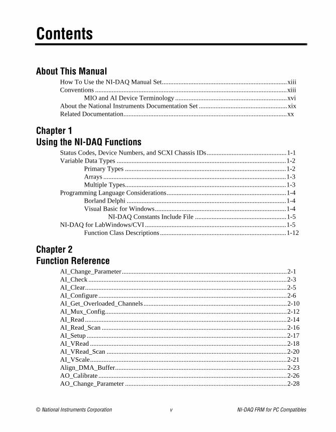
Contents
About This ManualHow To Use the NI-DAQ Manual Set...........................................................................xiiiConventions ...................................................................................................................xiii
MIO and AI Device Terminology ...................................................................xviAbout the National Instruments Documentation Set .....................................................xixRelated Documentation..................................................................................................xx
Chapter 1Using the NI-DAQ Functions
Status Codes, Device Numbers, and SCXI Chassis IDs................................................1-1Variable Data Types ......................................................................................................1-2
Primary Types .................................................................................................1-2Arrays ..............................................................................................................1-3Multiple Types.................................................................................................1-3
Programming Language Considerations........................................................................1-4Borland Delphi ................................................................................................1-4Visual Basic for Windows...............................................................................1-4
NI-DAQ Constants Include File .......................................................1-5NI-DAQ for LabWindows/CVI .....................................................................................1-5
Function Class Descriptions ............................................................................1-12
Chapter 2Function Reference
AI_Change_Parameter...................................................................................................2-1AI_Check .......................................................................................................................2-3AI_Clear.........................................................................................................................2-5AI_Configure .................................................................................................................2-6AI_Get_Overloaded_Channels ......................................................................................2-10AI_Mux_Config.............................................................................................................2-12AI_Read .........................................................................................................................2-14AI_Read_Scan ...............................................................................................................2-16AI_Setup ........................................................................................................................2-17AI_VRead ......................................................................................................................2-18AI_VRead_Scan ............................................................................................................2-20AI_VScale......................................................................................................................2-21Align_DMA_Buffer.......................................................................................................2-23AO_Calibrate .................................................................................................................2-26AO_Change_Parameter .................................................................................................2-28

Contents
NI-DAQ FRM for PC Compatibles vi www.natinst.com
AO_Configure ............................................................................................................... 2-35AO_Update.................................................................................................................... 2-39AO_VScale.................................................................................................................... 2-40AO_VWrite ................................................................................................................... 2-42AO_Write ...................................................................................................................... 2-44Calibrate_1200 .............................................................................................................. 2-46Calibrate_DSA .............................................................................................................. 2-52Calibrate_E_Series ........................................................................................................ 2-55Calibrate_TIO................................................................................................................ 2-61Config_Alarm_Deadband.............................................................................................. 2-64Config_ATrig_Event_Message..................................................................................... 2-68Config_DAQ_Event_Message...................................................................................... 2-72Configure_HW_Analog_Trigger .................................................................................. 2-84CTR_Config .................................................................................................................. 2-91CTR_EvCount ............................................................................................................... 2-93CTR_EvRead................................................................................................................. 2-95CTR_FOUT_Config...................................................................................................... 2-97CTR_Period................................................................................................................... 2-99CTR_Pulse..................................................................................................................... 2-101CTR_Rate ...................................................................................................................... 2-105CTR_Reset .................................................................................................................... 2-107CTR_Restart .................................................................................................................. 2-108CTR_Simul_Op............................................................................................................. 2-109CTR_Square .................................................................................................................. 2-111CTR_State ..................................................................................................................... 2-114CTR_Stop...................................................................................................................... 2-115DAQ_Check .................................................................................................................. 2-116DAQ_Clear.................................................................................................................... 2-118DAQ_Config ................................................................................................................. 2-119DAQ_DB_Config.......................................................................................................... 2-122DAQ_DB_HalfReady.................................................................................................... 2-123DAQ_DB_Transfer ....................................................................................................... 2-125DAQ_Monitor ............................................................................................................... 2-127DAQ_Op........................................................................................................................ 2-130DAQ_Rate ..................................................................................................................... 2-133DAQ_Set_Clock............................................................................................................ 2-135DAQ_Start ..................................................................................................................... 2-137DAQ_StopTrigger_Config ............................................................................................ 2-141DAQ_to_Disk................................................................................................................ 2-143DAQ_VScale................................................................................................................. 2-146DIG_Block_Check ........................................................................................................ 2-148DIG_Block_Clear.......................................................................................................... 2-149DIG_Block_In ............................................................................................................... 2-150DIG_Block_Out ............................................................................................................ 2-153

Contents
© National Instruments Corporation vii NI-DAQ FRM for PC Compatibles
DIG_Block_PG_Config.................................................................................................2-155DIG_Change_Message_Config .....................................................................................2-159DIG_Change_Message_Control ....................................................................................2-162DIG_DB_Config............................................................................................................2-163DIG_DB_HalfReady .....................................................................................................2-165DIG_DB_Transfer .........................................................................................................2-167DIG_Filter_Config.........................................................................................................2-169DIG_Grp_Config ...........................................................................................................2-171DIG_Grp_Mode.............................................................................................................2-173DIG_Grp_Status ............................................................................................................2-176DIG_In_Grp...................................................................................................................2-178DIG_In_Line..................................................................................................................2-180DIG_In_Prt ....................................................................................................................2-182DIG_Line_Config ..........................................................................................................2-184DIG_Out_Grp ................................................................................................................2-186DIG_Out_Line ...............................................................................................................2-187DIG_Out_Prt..................................................................................................................2-189DIG_Prt_Config.............................................................................................................2-191DIG_Prt_Status..............................................................................................................2-194DIG_SCAN_Setup.........................................................................................................2-196DIG_Trigger_Config .....................................................................................................2-200Get_DAQ_Device_Info .................................................................................................2-203Get_NI_DAQ_Version ..................................................................................................2-206GPCTR_Change_Parameter ..........................................................................................2-207GPCTR_Config_Buffer .................................................................................................2-222GPCTR_Control ............................................................................................................2-224GPCTR_Read_Buffer ....................................................................................................2-227GPCTR_Set_Application...............................................................................................2-230GPCTR_Watch ..............................................................................................................2-264ICTR_Read ....................................................................................................................2-267ICTR_Reset ...................................................................................................................2-269ICTR_Setup ...................................................................................................................2-270Init_DA_Brds.................................................................................................................2-274Lab_ISCAN_Check .......................................................................................................2-282Lab_ISCAN_Op ............................................................................................................2-285Lab_ISCAN_Start..........................................................................................................2-289Lab_ISCAN_to_Disk.....................................................................................................2-293Line_Change_Attribute .................................................................................................2-296LPM16_Calibrate...........................................................................................................2-299MIO_Config...................................................................................................................2-300RTSI_Clear ....................................................................................................................2-302RTSI_Clock ...................................................................................................................2-303RTSI_Conn ....................................................................................................................2-305RTSI_DisConn...............................................................................................................2-310

Contents
NI-DAQ FRM for PC Compatibles viii www.natinst.com
SC_2040_Config ........................................................................................................... 2-311SCAN_Demux............................................................................................................... 2-313SCAN_Op...................................................................................................................... 2-315SCAN_Sequence_Demux ............................................................................................. 2-318SCAN_Sequence_Retrieve............................................................................................ 2-321SCAN_Sequence_Setup................................................................................................ 2-322SCAN_Setup ................................................................................................................. 2-325SCAN_Start................................................................................................................... 2-328SCAN_to_Disk.............................................................................................................. 2-334SCXI_AO_Write ........................................................................................................... 2-338SCXI_Cal_Constants..................................................................................................... 2-341SCXI_Calibrate ............................................................................................................. 2-350SCXI_Calibrate_Setup .................................................................................................. 2-354SCXI_Change_Chan ..................................................................................................... 2-356SCXI_Configure_Filter ................................................................................................. 2-357SCXI_Get_Chassis_Info ............................................................................................... 2-360SCXI_Get_Module_Info ............................................................................................... 2-362SCXI_Get_State ............................................................................................................ 2-364SCXI_Get_Status .......................................................................................................... 2-366SCXI_Load_Config....................................................................................................... 2-368SCXI_ModuleID_Read ................................................................................................. 2-369SCXI_MuxCtr_Setup .................................................................................................... 2-371SCXI_Reset ................................................................................................................... 2-373SCXI_Scale ................................................................................................................... 2-376SCXI_SCAN_Setup ...................................................................................................... 2-380SCXI_Set_Config.......................................................................................................... 2-383SCXI_Set_Gain ............................................................................................................. 2-387SCXI_Set_Input_Mode ................................................................................................. 2-389SCXI_Set_State............................................................................................................. 2-390SCXI_Set_Threshold..................................................................................................... 2-392SCXI_Single_Chan_Setup ............................................................................................ 2-394SCXI_Track_Hold_Control .......................................................................................... 2-395SCXI_Track_Hold_Setup.............................................................................................. 2-397Select_Signal ................................................................................................................. 2-401Set_DAQ_Device_Info ................................................................................................. 2-423Timeout_Config ............................................................................................................ 2-434WFM_Chan_Control..................................................................................................... 2-436WFM_Check ................................................................................................................. 2-438WFM_ClockRate........................................................................................................... 2-440WFM_DB_Config......................................................................................................... 2-445WFM_DB_HalfReady................................................................................................... 2-447WFM_DB_Transfer ...................................................................................................... 2-449WFM_from_Disk .......................................................................................................... 2-451WFM_Group_Control ................................................................................................... 2-454

Contents
© National Instruments Corporation ix NI-DAQ FRM for PC Compatibles
WFM_Group_Setup.......................................................................................................2-456WFM_Load....................................................................................................................2-458WFM_Op .......................................................................................................................2-462WFM_Rate.....................................................................................................................2-465WFM_Scale ...................................................................................................................2-467WFM_Set_Clock ...........................................................................................................2-469
Appendix AError Codes
Appendix BAnalog Input Channel, Gain Settings, and Voltage Calculation
Appendix CNI-DAQ Function Support
Appendix DTechnical Support Resources
Glossary
Index
FiguresFigure 2-1. High Alarm Deadband...........................................................................2-66Figure 2-2. Low Alarm Deadband ...........................................................................2-67Figure 2-3. Analog Trigger Event............................................................................2-71Figure 2-4. ND_BELOW_LOW_LEVEL ...............................................................2-86Figure 2-5. ND_ABOVE_HIGH_LEVEL...............................................................2-86Figure 2-6. ND_INSIDE_REGION.........................................................................2-87Figure 2-7. ND_HIGH_HYSTERESIS ...................................................................2-87Figure 2-8. ND_LOW_HYSTERESIS ....................................................................2-87Figure 2-9. Pulse Generation Timing.......................................................................2-103Figure 2-10. Pulse Timing for pulseWidth = 0.........................................................2-104Figure 2-11. Square Wave Timing.............................................................................2-113Figure 2-12. Digital Scanning Input Group Handshaking Connections ....................2-198Figure 2-13. Digital Scanning Output Group Handshaking Connections..................2-199Figure 2-14. Position Measurement for X1 Encoders................................................2-212Figure 2-15. Position Measurement for X2 Encoders................................................2-212

Contents
NI-DAQ FRM for PC Compatibles x www.natinst.com
Figure 2-16. Position Measurement for X4 Encoders ............................................... 2-213Figure 2-17. Position Measurement Using Two Pulse Encoders .............................. 2-213Figure 2-18. X4 Quadrature Decoding with Z indexing............................................ 2-216Figure 2-19. Simple Event Counting ......................................................................... 2-233Figure 2-20. Single Period Measurement .................................................................. 2-234Figure 2-21. Single Pulse Width Measurement ......................................................... 2-237Figure 2-22. Single Triggered Pulse Width Generation Measurement ..................... 2-239Figure 2-23. Two Signal Edge Separation Measurement .......................................... 2-242Figure 2-24. X4 Decoding Example with Z indexing ............................................... 2-244Figure 2-25. Single Pulse Generation........................................................................ 2-245Figure 2-26. Single Triggered Pulse Generation ....................................................... 2-247Figure 2-27. Retriggerable Pulse Generation ............................................................ 2-249Figure 2-28. Pulse Train Generation ......................................................................... 2-250Figure 2-29. Frequency Shift Keying ........................................................................ 2-252Figure 2-30. Buffered Event Counting ...................................................................... 2-254Figure 2-31. Buffered Period Measurement .............................................................. 2-256Figure 2-32. Buffered Period Measurement when No Source Edges Are
Present between Gate Edges ................................................................. 2-257Figure 2-33. Buffered Semi-Period Measurement..................................................... 2-258Figure 2-34. Buffered Semi-Period Measurement when No Source Edges
Are Present between Gate Edges .......................................................... 2-258Figure 2-35. Buffered Pulse Width Measurement ..................................................... 2-259Figure 2-36. Buffered Pulse Width when Gate Is High during Arming.................... 2-260Figure 2-37. Buffered Two-Signal Edge Separation Measurement .......................... 2-261Figure 2-38. Buffered Position Measurement ........................................................... 2-263Figure 2-39. Mode 0 Timing Diagram ...................................................................... 2-271Figure 2-40. Mode 1 Timing Diagram ...................................................................... 2-271Figure 2-41. Mode 2 Timing Diagram ...................................................................... 2-271Figure 2-42. Mode 3 Timing Diagram ...................................................................... 2-272Figure 2-43. Mode 4 Timing Diagram ...................................................................... 2-272Figure 2-44. Mode 5 Timing Diagram ...................................................................... 2-272
TablesTable 1. MIO and AI Devices............................................................................. xvii
Table 1-1. Status Values......................................................................................... 1-1Table 1-2. Primary Type Names ............................................................................ 1-2Table 1-3. The LabWindows/CVI Function Tree for Data Acquisition ................ 1-6Table 2-1. Parameter Settings for AI_Configure ................................................... 2-7Table 2-2. Port 0 Digital I/O Lines Reserved......................................................... 2-13Table 2-3. Reglitching Parameters for Permissible Devices.................................. 2-29Table 2-4. Voltage or Current Output Parameters ................................................. 2-29Table 2-5. Parameter Values for FIFO Transfer Conditions.................................. 2-30

Contents
© National Instruments Corporation xi NI-DAQ FRM for PC Compatibles
Table 2-6. Default Values for FIFO Transfer Condition ........................................2-31Table 2-7. Parameter Setting Information for Output Enable ................................2-32Table 2-8. Parameter Setting Information for Output Attenuation.........................2-33Table 2-9. Possible Calibrate_1200 Parameter Values .....................................2-48Table 2-10. DAQEvent Messages ............................................................................2-75Table 2-11. Valid Counters and External Timing Signals for DAQEvent = 9 ........2-79Table 2-12. Usable Parameters for Different DAQEvent Codes.............................2-80Table 2-13. Legal Values for gpctrNum Parameter..................................................2-208Table 2-14. Legal Values for paramValue when paramID = ND_SOURCE
and gpctrNum =ND_Counter_X. ..........................................................2-209Table 2-15. Definition of Other Counter for paramValue Set to
ND_OTHER_GPCTR_TC....................................................................2-210Table 2-16. Default Source Selection for ND_SIMPLE_EVENT_CNT or
ND_BUFFERED_EVENT_CNT..........................................................2-210Table 2-17. Legal Values for paramValue when paramID = ND_GATE and
gpctrNum =ND_COUNTER_X. ...........................................................2-214Table 2-18. Default Gate Selection...........................................................................2-215Table 2-19. Default Aux Line Selection...................................................................2-218Table 2-20. Legal Values for paramValue when
paramID = ND_INITIAL_COUNT . .......................................................2-218Table 2-21. Legal Values for paramValue when paramID = ND_COUNT_1,
ND_COUNT_2, ND_COUNT_3, and ND_COUNT_4..............................2-219Table 2-22. Default Up/Down Selection ..................................................................2-220Table 2-23. Legal Values for the action Parameter ..................................................2-225Table 2-24. Descriptions for application ..................................................................2-231Table 2-25. Terminal Count......................................................................................2-233Table 2-26. AT-AO-6/10, DAQPad-6713, and DIO-32F RTSI Bus Signals ...........2-305Table 2-27. DIO 6533 RTSI Bus Signals .................................................................2-306Table 2-28. SCXI Module Scan List ........................................................................2-372Table 2-29. MIO or AI Scan List..............................................................................2-372Table 2-30. Possible Values for signal .....................................................................2-403Table 2-31. Legal Parameters for the 660X Devices................................................2-414Table 2-32. E Series and 671X Signal Name Equivalencies ....................................2-420Table 2-33. RTSI Bus Line and VXIbus Trigger Mapping......................................2-421Table 2-34. RTSI Bus Line and PXI Bus Trigger Mapping.....................................2-421
Table A-1. Error Code Summary.............................................................................A-1
Table B-1. Valid Analog Input Channel Settings....................................................B-1Table B-2. Valid Internal Analog Input Channels...................................................B-2Table B-3. Internal Channel Purposes for Analog Input Devices ...........................B-6Table B-4. Valid Gain Settings ...............................................................................B-7Table B-5. The Values of maxReading and maxVolt .............................................B-8

Contents
NI-DAQ FRM for PC Compatibles xii www.natinst.com
Table C-1. MIO and AI Device Functions.............................................................. C-1Table C-2. Lab/516/DAQCard-500/700 Functions ................................................ C-5Table C-3. DSA Device Functions ......................................................................... C-8Table C-4. Analog Output Family Functions.......................................................... C-10Table C-5. Digital I/O Family Functions ................................................................ C-12Table C-6. Timing Device Functions...................................................................... C-13Table C-7. SCXI Functions..................................................................................... C-15

© National Instruments Corporation xiii NI-DAQ FRM for PC Compatibles
About This Manual
The NI-DAQ Function Reference Manual for PC Compatibles is for users of the NI-DAQ software for PC compatibles version 6.6. NI-DAQ software is a powerful application programming interface (API) between your data acquisition (DAQ) application and the National Instruments DAQ devices.
How To Use the NI-DAQ Manual SetYou should begin by reading the NI-DAQ User Manual for PC Compatibles. Chapter 1, Introduction to NI-DAQ, contains a flowchart that illustrates the sequence of steps you should take to learn about and get started with NI-DAQ software.
When you are familiar with the material in the NI-DAQ User Manual for PC Compatibles, you can use the NI-DAQ Function Reference Manual for PC Compatibles, which contains detailed descriptions of the NI-DAQ functions. You also can use the Windows help file NIDAQPC.HLP, which contains all of the function reference material. Other documentation includes the DAQ Hardware Overview Guide, and the Measurement & Automation Explorer help file.
ConventionsThe following conventions appear in this manual:
* An asterisk following a signal name indicates an active low signal.
This icon denotes a note, which alerts you to important information.
This icon denotes a caution, which advises you of precautions to take to avoid injury, data loss, or a system crash.
1102/B/C modules Refers to the SCXI-1102, SCXI-1102B, and SCXI-1102C modules and the VXI-SC-1102, VXI-SC-1102B, and VXI-SC-1102C submodules.
1200/1200 AI device Refers to DAQCard-1200, DAQPad-1200, Lab-PC-1200, Lab-PC-1200AI, PCI-1200, and SCXI-1200.
1394 Refers to a high-speed external bus that implements the IEEE 1394 serial bus protocol.

About This Manual
NI-DAQ FRM for PC Compatibles xiv www.natinst.com
12-bit device These MIO and AI devices are listed in Table 1.
16-bit device These MIO and AI devices are listed in Table 1.
445X device Refers to the PCI-4451, PCI-4452, PCI-4453, and PCI-4454.
455X device Refers to the NI 4551 and NI 4552.
516 device Refers to the DAQCard-516 and PC-516.
54XX device Refers to the AT-5411 and PCI-5411.
611X device Refers to the PCI-6110E and PCI-6111E.
6025E device Refers to the PCI-6025E and PXI-6025E.
6052E device Refers to the PCI-6052E, PXI-6052E, and DAQPad-6052E for 1394.
652X device Refers to the PCI-6527and PXI-6527.
660X device Refers to the PCI-6601, PCI-6602, PXI-6602, PCI-6608, and PXI-6608.
6602 device Refers to the PCI-6602 and PXI-6602.
6703 device Refers to the PCI-6703 and PXI-6703.
6704 device Refers to the PCI-6704 and PXI-6704.
671X device Refers to the PCI-6711, PXI-6711, PCI-6713, and PXI-6713.
AI device These analog input devices are listed in Table 1.
bold Bold text denotes items that you must select or click on in the software, such as menu items and dialog box options. Bold text also denotes parameter names.
DAQCard-500/700 Refers to the DAQCard-500 and DAQCard-700.
DIO 6533 Refers to the AT-DIO-32HS, PCI-DIO-32HS, DAQCard-6533, and PXI-6533.
DIO-24 (6503) Refers to the PC-DIO-24, PC-DIO-24PnP, DAQCard-DIO-24, and PCI-6503.
DIO-32F Refers to the AT-DIO-32F.

About This Manual
© National Instruments Corporation xv NI-DAQ FRM for PC Compatibles
DIO-96 Refers to the PC-DIO-96PnP, PCI-DIO-96, DAQPad-6507, DAQPad-6508, and PXI-6508.
DIO device Refers to any DIO-24, DIO-32, DIO-6533 (DIO-32HS), DIO-96, VXI-DIO-128, or DAQPad DIO.
DSA device Refers to the PCI-4451, PCI-4452, PCI-4453, PCI-4454, NI 4551, and NI 4552.
E Series device These are MIO and AI devices. Refer to Table 1 for a complete list of these devices.
italic Italic text denotes variables, emphasis, a cross reference, or an introduction to a key concept. This font also denotes text that is a placeholder for a word or value that you must supply.
Lab and 1200 analog Refers to the DAQCard-1200, DAQPad-1200, Lab-PC+, Lab-PC-1200,output device PCI-1200, and SCXI-1200.
Lab and 1200 device Refers to the DAQCard-1200, DAQPad-1200, Lobed+, Lab-PC-1200, Lab-PC-1200AI, PCI-1200, and SCXI-1200.
LPM device Refers to the PC-LPM-16 and PC-LPM-16PnP.
MIO device Refers to multifunction I/O devices. See Table 1 for a list of these devices.
MIO-16XE-50 device Refers to the AT-MIO-16XE-50, DAQPad-MIO-16XE-50, and NEC-MIO-16XE-50, and PCI-MIO-16XE-50.
MIO-64 Refers to MIO devices with 64 AI channels, such as the AT-MIO-64E-3, PCI-6031E, PCI-6033E, PCI-6071E, VXI-MIO-64E-1, and VXI-MIO-64XE-10.
monospace Text in this font denotes text or characters that you should enter from the keyboard, sections of code, programming examples, and syntax examples. This font is also used for the proper names of disk drives, paths, directories, programs, subprograms, subroutines, device names, functions, operations, variables, filenames and extensions, and code excerpts.
monospace italic Italic text in this font denotes text that is a placeholder for a word or value that you must supply.
NI-DAQ Refers to the NI-DAQ software for PC compatibles, unless otherwise noted.
NI-TIO based device Refers to the NI 4551, NI 4552, PCI-6601, PCI-6602, PXI-6602, PCI-6608, and PXI-6608.

About This Manual
NI-DAQ FRM for PC Compatibles xvi www.natinst.com
PC Refers to the IBM PC/XT, IBM PC AT, and compatible computers.
PCI Series Refers to the National Instruments products that use the high-performance expansion bus architecture originally developed by Intel.
PXI Refers to PCI extensions for instrumentation that are derived from the CompactPCI standard.
remote SCXI Refers to an SCXI configuration where either an SCXI-2000 chassis or an SCXI-2400 remote communications module is connected to the PC serial port.
SCXI-1102/B/C Refers to the SCXI-1102, SCXI-1102B, and SCXI-1102C devices.
SCXI-1120/D Refers to the SCXI-1120 and SCXI-1120D.
SCXI analog input Refers to the SCXI-1100, SCXI-1101, SCXI-1102, SCXI-1104, module SCXI-1112, SCXI-1120, SCXI-1120D, SCXI-1121, SCXI-1122,
SCXI-1125, SCXI-1140, SCXI-1141, SCXI-1142, and SCXI-1143.
SCXI chassis Refers to the SCXI-1000, SCXI-1000DC, SCXI-1001, and SCXI-2000.
SCXI digital module Refers to the SCXI-1160, SCXI-1161, SCXI-1162, SCXI-1162HV, SCXI-1163, and SCXI-1163R.
simultaneous sampling Refers to the PCI-6110E, PCI-6111E, PCI-4451, PCI-4452, PCI-4551, device PCI-4552, PCI-4453, and PCI-4454.
VXI-MIO device Refers to the VXI-MIO-64E-1 and VXI-MIO-64XE-10.
VXI-SC-1102/B/C Refers to the VXI-SC-1102, VXI-SC-1102B, and VXI-SC-1102C.
MIO and AI Device TerminologyThis manual uses generic terms to describe groups of devices whenever possible. The generic terms for the MIO and AI devices are based on the number of bits, the platform, and the functionality. These devices are collectively known as the E Series devices. Table 1 lists each MIO and AI device and the possible board type for each.

About This Manual
© National Instruments Corporation xvii NI-DAQ FRM for PC Compatibles
Table 1. MIO and AI Devices
Device Board Type
Numberof SE
Channels Bit Type
AT-AI-16XE-10 AI 16 16-bit AT
AT-MIO-16DE-10 MIO 16 12-bit AT
AT-MIO-16E-1 MIO 16 12-bit AT
AT-MIO-16E-2 MIO 16 12-bit AT
AT-MIO-16E-10 MIO 16 12-bit AT
AT-MIO-16F-5 MIO 16 12-bit AT
AT-MIO-16XE-10 MIO 16 16-bit AT
AT-MIO-16XE-50 MIO 16 16-bit AT
AT-MIO-64E-3 MIO 64 12-bit AT
AT-MIO-64F-5 MIO 64 12-bit AT
DAQCard-6023E AI 16 12-bit PCMCIA
DAQCard-6024E MIO 16 12-bit PCMCIA
DAQCard-6062E MIO 16 12-bit PCMCIA
DAQCard-AI-16E-4 AI 16 12-bit PCMCIA
DAQCard-AI-16XE-50 AI 16 16-bit PCMCIA
DAQPad-MIO-16XE-50 MIO 16 16-bit Parallel Port
DAQPad-6020E MIO 16 12-bit USB
DAQPad-6052E MIO 16 16-bit 1394
DAQPad-6070E MIO 16 12-bit 1394
NEC-AI-16E-4 AI 16 12-bit NEC
NEC-AI-16XE-50 AI 16 16-bit NEC
NEC-MIO-16E-4 MIO 16 12-bit NEC
NEC-MIO-16XE-50 MIO 16 16-bit NEC
PCI-6023E AI 16 12-bit PCI

About This Manual
NI-DAQ FRM for PC Compatibles xviii www.natinst.com
PCI-6024E MIO 16 12-bit PCI
PCI-6025E MIO 16 12-bit PCI
PCI-6031E (MIO-64XE-10) MIO 64 16-bit PCI
PCI-6032E (AI-16XE-10) AI 16 16-bit PCI
PCI-6033E (AI-64XE-10) AI 64 16-bit PCI
PCI-6034E AI 16 16-bit PCI
PCI-6035E MIO 16 16-bit AI 12-bit AO
PCI
PCI-6052E MIO 16 16-bit PCI
PCI-6071E (MIO-64E-1) MIO 64 12-bit PCI
PCI-6110E MIO 4 diff. only 12-bit AI16-bit AO
PCI
PCI-6111E MIO 2 diff. only 12-bit AI16-bit AO
PCI
PCI-MIO-16E-1 MIO 16 12-bit PCI
PCI-MIO-16E-4 MIO 16 12-bit PCI
PCI-MIO-16XE-10 MIO 16 16-bit PCI
PCI-MIO-16XE-50 MIO 16 16-bit PCI
PXI-6011E MIO 16 16-bit PXI
PXI-6023E AI 16 12-bit PXI
PXI-6024E MIO 16 12-bit PXI
PXI-6025E MIO 16 12-bit PXI
PXI-6030E MIO 16 16-bit PXI
PXI-6031E MIO 64 16-bit PXI
PXI-6034E AI 16 16-bit PXI
Table 1. MIO and AI Devices (Continued)
Device Board Type
Numberof SE
Channels Bit Type

About This Manual
© National Instruments Corporation xix NI-DAQ FRM for PC Compatibles
About the National Instruments Documentation SetThe NI-DAQ Function Reference Manual for PC Compatibles is one piece of the documentation set for your DAQ system. You might have any of several types of manuals, depending on the hardware and software in your system. Use these manuals as follows:
• Getting Started with SCXI—If you are using SCXI, this is the first manual you should read. It gives an overview of the SCXI system and contains the most commonly needed information for the modules, chassis, and software.
• Your SCXI hardware user manuals—These manuals contain detailed information about signal connections and module configuration. They also explain in greater detail how the module works and contain application hints.
• Your DAQ hardware user manuals—These manuals have detailed information about the DAQ hardware that plugs into or is connected to your computer. Use these manuals for hardware installation and configuration instructions, specification information about your DAQ hardware, and application hints.
• Software documentation—Examples of software documentation you might have are the ComponentWorks, LabVIEW and LabWindows/CVI, VirtualBench, and NI-DAQ documentation. After you have set up your hardware system, use either the application software or the NI-DAQ documents to help you write your application. If you have a large and complicated system, it is worthwhile to look through the software manuals before you configure your hardware.
PXI-6035E MIO 16 16-bit AI 12-bit AO
PXI
PXI-6040E MIO 16 12-bit PXI
PXI-6052E MIO 16 16-bit PXI
PXI-6070E MIO 16 12-bit PXI
VXI-MIO-64E-1 MIO 64 12-bit VXI
VXI-MIO-64XE-10 MIO 64 16-bit VXI
Table 1. MIO and AI Devices (Continued)
Device Board Type
Numberof SE
Channels Bit Type

About This Manual
NI-DAQ FRM for PC Compatibles xx www.natinst.com
• Accessory installation guides or manuals—If you are using accessory products, read the terminal block and cable assembly installation guides or accessory board user manuals. They explain how to physically connect the relevant pieces of the system. Consult these guides when you are making your connections.
• SCXI Chassis User Manual—If you are using SCXI, read this manual for maintenance information on the chassis and installation instructions.
Related DocumentationThe following documents contain information you may find useful as you read this manual.
For detailed hardware information, refer to the user manual included with each board. You can also review the following manuals:
• Omega Temperature Handbook
• NIST Monograph 125, Thermocouple Reference Tables

© National Instruments Corporation 1-1 NI-DAQ FRM for PC Compatibles
1Using the NI-DAQ Functions
This chapter contains important information about how to apply the function descriptions in this manual to your programming language and environment.
When you are familiar with the material in the NI-DAQ User Manual for PC Compatibles, you can use this manual for detailed information about each NI-DAQ function.
Status Codes, Device Numbers, and SCXI Chassis IDsEvery NI-DAQ function is of the following form:
status = Function_Name (parameter 1, parameter 2, … parameter n)
where n ≥ 0. Each function returns a value in the status variable that indicates the success or failure of the function, as shown in Table 1-1.
Note In all applications, status is always a 16-bit integer. Appendix A, Error Codes, contains a list of error codes.
Parameter tables follow the NI-DAQ function format and purpose. The first parameter to almost every NI-DAQ function is the device number of the DAQ device you want NI-DAQ to use for the given operation. After you follow the installation and configuration instructions in the NI-DAQ release notes and Chapter 1, Introduction to NI-DAQ, of the NI-DAQ User Manual for PC Compatibles, you can use Measurement & Automation Explorer, to
Table 1-1. Status Values
Status Result
Negative Function did not execute because of an error
Zero Function completed successfully
Positive Function executed but with a potentially serious side effect

Chapter 1 Using the NI-DAQ Functions
NI-DAQ FRM for PC Compatibles 1-2 www.natinst.com
determine the device number for each device you have installed in the system, or to verify your device numbers. You can use multiple DAQ devices in one application; to do so, pass the appropriate device number to each function.
If you are using SCXI, you must pass the chassis ID that you assigned to your SCXI chassis in the configuration utility to the SCXI functions you use. For many of the SCXI functions, you must also pass the module slot number of the module you want to use. The slots in the SCXI chassis are numbered from left to right, beginning with slot 1. The controller on the left side of the chassis is referred to as Slot 0. You can use the configuration utility to verify your chassis IDs and your module slot numbers.
Variable Data TypesThe NI-DAQ API is identical in Windows 98/95 and Windows NT. Every function description has a parameter table that lists the data types in each of the environments. LabWindows/CVI uses the same types as Windows. The following sections describe the notation used in those parameter tables and throughout the manual for variable data types.
Primary TypesTable 1-2 shows the primary type names and their ranges.
Table 1-2. Primary Type Names
Type Name Description Range
Type
C/C++ Visual BASICPascal
(Borland Delphi)
i8 8-bit ASCII character
–128 to 127 char Not supported by BASIC. For functions that require character arrays, use string types instead. See the STR description.
Byte
i16 16-bit signed integer
–32,768 to 32,767 short Integer (for example: deviceNum% )
SmallInt

Chapter 1 Using the NI-DAQ Functions
© National Instruments Corporation 1-3 NI-DAQ FRM for PC Compatibles
ArraysWhen a primary type is inside square brackets (for example, [i16]) an array of the type named is required for that parameter.
Multiple TypesSome parameters can be in multiple types. Combinations of the primary types separated by commas denote parameters with this ability, as in the following example:
[i16], [f32]
u16 16-bit unsigned integer
0 to 65,535 unsignedshort
Not supported by BASIC. For functions that require unsigned integers, use the signed integer type instead. See the i16 description.
Word
i32 32-bit signed integer
–2,147,483,648 to 2,147,483,647
long Long (for example: count& )
LongInt
u32 32-bit unsigned integer
0 to 4,294,967,295 unsigned long
Not supported by BASIC. For functions that require unsigned long integers, use the signed long integer type instead. See the i32 description.
Cardinal (in 32-bit operating
systems). Refer to the i32
description.
f32 32-bit single-precision floating point
–3.402823 × 1038 to 3.402823 × 1038
float Single (for example:num! )
Single
f64 64-bit double-precision floating point
–1.797683134862315 × 10308 to
1.797683134862315 × 10308
double Double (for example:voltage# )
Double
STR BASIC or Pascal character string
— Use character array terminated
by the null character \0
String (for example: filename$ )
String
Table 1-2. Primary Type Names (Continued)
Type Name Description Range
Type
C/C++ Visual BASICPascal
(Borland Delphi)

Chapter 1 Using the NI-DAQ Functions
NI-DAQ FRM for PC Compatibles 1-4 www.natinst.com
The previous example describes a parameter that can accept an array of signed integers or an array of floating-point numbers.
Programming Language ConsiderationsApart from the data type differences, there are a few language-dependent considerations you need to be aware of when you use the NI-DAQ API. Read the following sections that apply to your programming language.
Note Be sure to include the NI-DAQ function prototype files by including the appropriate NI-DAQ header file in your source code.
Note Refer to Chapter 2, Fundamentals of Building Windows Applications, in the NI-DAQ User Manual for PC Compatibles for further programming details.
Borland DelphiWhen you pass arrays to NI-DAQ functions using Borland Delphi in Windows, you need to pass a pointer to the array. You can either declare an array and pass the array address to the NI-DAQ function, or you can declare a pointer, dynamically allocate memory for the pointer, and pass the pointer directly to the NI-DAQ function. For example:
var
buffer : array [1..1000] of Integer;
bufPtr : ^Integer;
status := DAQ_Start (device, chan, gain, @buffer, count,
timebase, sampInterval);
or
(* allocate memory for bufPtr first using AllocMem or
New *)
status := DAQ_Start (device, chan, gain, bufPtr, count,
timebase, sampInterval);
Visual Basic for WindowsWhen you pass arrays to NI-DAQ functions using Visual Basic for Windows, you need to pass the first element of the array by reference. For example, you would call the DAQ_Start function using the following syntax:
status% = DAQ_Start (device%, chan%, gain%, buffer%(0),
count&, timebase%, sampInterval%)
Chapter 1 Using the NI-DAQ Functions
© National Instruments Corporation 1-5 NI-DAQ FRM for PC Compatibles
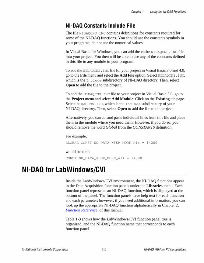
NI-DAQ Constants Include FileThe file NIDAQCNS.INC contains definitions for constants required for some of the NI-DAQ functions. You should use the constants symbols in your programs; do not use the numerical values.
In Visual Basic for Windows, you can add the entire NIDAQCNS.INC file into your project. You then will be able to use any of the constants defined in this file in any module in your program.
To add the NIDAQCNS.INC file for your project in Visual Basic 3.0 and 4.0, go to the File menu and select the Add File option. Select NIDAQCNS.INC, which is the Include subdirectory of NI-DAQ directory. Then, select Open to add the file to the project.
To add the NIDAQCNS.INC file to your project in Visual Basic 5.0, go to theProject menu and select Add Module. Click on the Existing tab page. Select NIDAQCNS.INC, which is the Include subdirectory of your NI-DAQ directory. Then, select Open to add the file to the project.
Alternatively, you can cut and paste individual lines from this file and place them in the module where you need them. However, if you do so, you should remove the word Global from the CONSTANTS definition.
For example,
GLOBAL CONST ND_DATA_XFER_MODE_AI& = 14000
would become:
CONST ND_DATA_XFER_MODE_AI& = 14000
NI-DAQ for LabWindows/CVIInside the LabWindows/CVI environment, the NI-DAQ functions appear in the Data Acquisition function panels under the Libraries menu. Each function panel represents an NI-DAQ function, which is displayed at the bottom of the panel. The function panels have help text for each function and each parameter; however, if you need additional information, you can look up the appropriate NI-DAQ function alphabetically in Chapter 2, Function Reference, of this manual.
Table 1-3 shows how the LabWindows/CVI function panel tree is organized, and the NI-DAQ function name that corresponds to each function panel.

Chapter 1 Using the NI-DAQ Functions
NI-DAQ FRM for PC Compatibles 1-6 www.natinst.com
Table 1-3. The LabWindows/CVI Function Tree for Data Acquisition
LabWindows/CVI Function Panel NI-DAQ Function
Data Acquisition
Initialization/Utilities
Initialize Board Init_DA_Brds
Configure Timeout Timeout_Config
Get Device Information Get_DAQ_Device_Info
Set Device Information Set_DAQ_Device_Info
Align DMA Buffer Align_DMA_Buffer
Get DAQ Library Version Get_NI_DAQ_Version
Select Signals Select_Signal
Config Analog Trigger Configure_HW_Analog_Trigger
Change Line Attribute Line_Change_Attribute
Board Config & Calibrate
Configure MIO Boards MIO_Config
Configure AMUX Boards AI_Mux_Config
Configure SC-2040 SC_2040_Config
Calibrate E-Series Calibrate_E_Series
Calibrate LPM-16 LPM16_Calibrate
Calibrate Analog Output AO_Calibrate
Calibrate 1200 Devices Calibrate_1200
Calibrate DSA Devices Calibrate_DSA
Calibrate TIO Devices Calibrate_TIO
Analog Input
Single Point
Measure Voltage AI_VRead
Clear Analog Input AI_Clear
Read Analog Binary AI_Read
Scale Binary to Voltage AI_VScale

Chapter 1 Using the NI-DAQ Functions
© National Instruments Corporation 1-7 NI-DAQ FRM for PC Compatibles
Setup Analog Input AI_Setup
Check Analog Input AI_Check
Configure Analog Input AI_Configure
Change Analog Input Parameter AI_Change_Parameter
Multiple Point
Acquire Single Channel DAQ_Op
Scan Multiple Channels SCAN_Op
Scan Lab Channels Lab_ISCAN_Op
Single Scan Binary AI_Read_Scan
Single Scan Voltage AI_VRead_Scan
Single Channel to Disk DAQ_to_Disk
Multiple Chans to Disk SCAN_to_Disk
Scan Lab Chans to Disk Lab_ISCAN_to_Disk
Low-Level Functions
Convert DAQ Rate DAQ_Rate
Start DAQ DAQ_Start
Setup Scan SCAN_Setup
Setup Sequence of Scans SCAN_Sequence_Setup
Retrieve Scan Sequence SCAN_Sequence_Retrieve
Start Scan SCAN_Start
Check DAQ or Scan DAQ_Check
Assign Rate to DAQ Group DAQ_Set_Clock
Monitor DAQ or Scan DAQ_Monitor
Start Lab Scan Lab_ISCAN_Start
Check Lab Scan Lab_ISCAN_Check
Clear DAQ or Scan DAQ_Clear
Scale DAQ or Scan DAQ_VScale
Table 1-3. The LabWindows/CVI Function Tree for Data Acquisition (Continued)
LabWindows/CVI Function Panel NI-DAQ Function

Chapter 1 Using the NI-DAQ Functions
NI-DAQ FRM for PC Compatibles 1-8 www.natinst.com
Reorder Scan Data SCAN_Demux
Reorder Scan Seq Data SCAN_Sequence_Demux
Configure DAQ DAQ_Config
Config DAQ Pretrigger DAQ_StopTrigger_Config
Enable Double Buffering DAQ_DB_Config
Is Half Buffer Ready? DAQ_DB_HalfReady
Half Buffer to Array DAQ_DB_Transfer
Set DAQ Clock Rate DAQ_Set_Clock
Get Overloaded Channels AI_Get_Overloaded_Channels
Analog Output
Single Point
Generate Voltage AO_VWrite
Scale Voltage to Binary AO_VScale
Write Analog Binary AO_Write
Update Analog DACs AO_Update
Configure Analog Output AO_Configure
Change Analog Output Parameter AO_Change_Parameter
Waveform Generation
Generate WFM from Array WFM_Op
Generate WFM from Disk WFM_from_Disk
Low-Level Functions
Scale Waveform Buffer WFM_Scale
Convert Waveform Rate WFM_Rate
Assign Waveform Group WFM_Group_Setup
Load Waveform Buffer WFM_Load
Assign Rate to WFM Group WFM_ClockRate
Control Waveform Group WFM_Group_Control
Table 1-3. The LabWindows/CVI Function Tree for Data Acquisition (Continued)
LabWindows/CVI Function Panel NI-DAQ Function
Chapter 1 Using the NI-DAQ Functions
© National Instruments Corporation 1-9 NI-DAQ FRM for PC Compatibles
Pause/Resume WFM Channel WFM_Chan_Control
Check Waveform Channel WFM_Check
Enable Double Buffering WFM_DB_Config
Is Half Buffer Ready? WFM_DB_HalfReady
Copy Array to WFM Buffer WFM_DB_Transfer
Set WFM Group Rate WFM_Set_Clock
Digital Input/Output
Configure Port DIG_Prt_Config
Configure Line DIG_Line_Config
Read Port (32-bit) DIG_In_Prt
Read Line DIG_In_Line
Write Port (32-bit) DIG_Out_Prt
Write Line DIG_Out_Line
Get Port Status DIG_Prt_Status
Group Mode
Configure Group DIG_Grp_Config
Read Group DIG_In_Grp
Write Group DIG_Out_Grp
Get Group Status DIG_Grp_Status
Set Group Mode DIG_Grp_Mode
Block Transfer
Read Block DIG_Block_In
Write Block DIG_Block_Out
Check Block DIG_Block_Check
Clear Block DIG_Block_Clear
Set Up Pattern Generation DIG_Block_PG_Config
Configure Digital Trigger DIG_Trigger_Config
Table 1-3. The LabWindows/CVI Function Tree for Data Acquisition (Continued)
LabWindows/CVI Function Panel NI-DAQ Function

Chapter 1 Using the NI-DAQ Functions
NI-DAQ FRM for PC Compatibles 1-10 www.natinst.com
Set Up Digital Scanning DIG_SCAN_Setup
Enable Double Buffering DIG_DB_Config
Is Half Buffer Ready? DIG_DB_HalfReady
Transfer To/From Array DIG_DB_Transfer
Change Notification
Configure Change Notification DIG_Change_Message_Config
Control Change Notification DIG_Change_Message_Control
Filtering
Configure Digital Filtering DIG_Filter_Config
SCXI
Load SCXI Configuration SCXI_Load_Config
Change Configuration SCXI_Set_Config
Get Chassis Config Info SCXI_Get_Chassis_Info
Get Module Config Info SCXI_Get_Module_Info
Read Module ID Register SCXI_ModuleID_Read
Reset SCXI SCXI_Reset
Set Up Single AI Channel SCXI_Single_Chan_Setup
Set Up Muxed Scanning SCXI_SCAN_Setup
Set Up Mux Counter SCXI_MuxCtr_Setup
Set Up Track/Hold SCXI_Track_Hold_Setup
Control Track/Hold State SCXI_Track_Hold_Control
Select Gain SCXI_Set_Gain
Configure Filter SCXI_Configure_Filter
Select Scanning Mode SCXI_Set_Input_Mode
Change AI Channel SCXI_Change_Chan
Scale SCXI Data SCXI_Scale
Write to AO Channel SCXI_AO_Write
Table 1-3. The LabWindows/CVI Function Tree for Data Acquisition (Continued)
LabWindows/CVI Function Panel NI-DAQ Function

Chapter 1 Using the NI-DAQ Functions
© National Instruments Corporation 1-11 NI-DAQ FRM for PC Compatibles
Set Digital or Relay State SCXI_Set_State
Get Digital or Relay State SCXI_Get_State
Get Status Register SCXI_Get_Status
Set Up Calibration Mode SCXI_Calibrate_Setup
Calibrate SCXI Module SCXI_Calibrate
Change Cal Constants SCXI_Cal_Constants
Set Threshold Values SCXI_Set_Threshold
Counter/Timer
DAQ-STC and NI-TIO Counters
Select Ctr Application GPCTR_Set_Application
Change Ctr Parameter GPCTR_Change_Parameter
Configure Ctr Buffer GPCTR_Config_Buffer
Control Ctr Operation GPCTR_Control
Monitor Ctr Properties GPCTR_Watch
Read Ctr Buffer GPCTR_Read_Buffer
Am9513 Counters (CTR)
Configure Counter CTR_Config
Count Events CTR_EvCount
Count Periods CTR_Period
Read Counter CTR_EvRead
Stop Counter CTR_Stop
Restart Counter CTR_Restart
Reset Counter CTR_Reset
Get Counter Output State CTR_State
Convert CTR Rate CTR_Rate
Generate Pulse CTR_Pulse
Generate Square Wave CTR_Square
Table 1-3. The LabWindows/CVI Function Tree for Data Acquisition (Continued)
LabWindows/CVI Function Panel NI-DAQ Function

Chapter 1 Using the NI-DAQ Functions
NI-DAQ FRM for PC Compatibles 1-12 www.natinst.com
Function Class DescriptionsThe Initialization/Utilities class is used for general board initialization and configuration, configuration retrieval, and setting NI-DAQ properties. This class also contains several useful utility functions.
The Board Config & Calibrate class performs calibration and configuration for specific types of boards.
The Analog Input class contains the classes of functions that perform A/D conversions.
The Single Point class of Analog Input functions performs analog-to-digital (A/D) conversions of a single sample.
Generate Freq OUT Signal CTR_FOUT_Config
Operate Multi Counters CTR_Simul_Op
8253 Counters (ICTR)
Setup Interval Counter ICTR_Setup
Read Interval Counter ICTR_Read
Reset Interval Counter ICTR_Reset
RTSI Bus
Connect RTSI RTSI_Conn
Disconnect RTSI RTSI_DisConn
Clear RTSI RTSI_Clear
Clock RTSI RTSI_Clock
Event Messaging
Config Alarm Deadband Config_Alarm_Deadband
Config Analog Trigger Event Config_ATrig_Event_Message
Config Event Message Config_DAQ_Event_Message
Table 1-3. The LabWindows/CVI Function Tree for Data Acquisition (Continued)
LabWindows/CVI Function Panel NI-DAQ Function

Chapter 1 Using the NI-DAQ Functions
© National Instruments Corporation 1-13 NI-DAQ FRM for PC Compatibles
The Multiple Point class performs clocked, buffered multiple A/D conversions typically used to capture waveforms. This class includes high-level functions and a Low-Level Functions subclass. The high-level functions are synchronous; that is, your application is blocked while these functions are performing the requested number of A/D conversions. The low-level functions are asynchronous; that is, your application continues to run while the board performs A/D conversions in the background. The low-level functions also include the double-buffered functions. The Analog Output class contains the function classes that perform digital-to-analog (D/A) conversions.
The Single Point class of Analog Output functions performs single D/A conversions.
The Waveform Generation class performs buffered analog output. The Waveform Generation functions generate waveforms from data contained in an array or a disk file. The Low-Level Functions subclass provides a finer level of control in generating multiple D/A conversions.
The Digital Input/Output class performs digital input and output operations. It also contains two subclasses. Group Mode is a subclass of the Digital Input/Output class that contains functions for handshaked digital input and output operations. Block Transfer is a subclass of the Group Mode class that contains functions for handshaked or clocked, buffered or double-buffered digital input and output operations.
The Change Notification class sets up conditions for sending messages to your application when certain digital lines change state.
The Filtering class performs signal conditioning of selected digital input lines.
The SCXI class configures the SCXI line of signal conditioning products.
The Counter/Timer class of function panels performs counting and timing operations. DAQ-STC and NI-TIO Counters is a subclass of Counter/Timer that contains functions that perform operations on the DAQ-STC counters on the E Series and NI-TIO devices. Am9513 Counters (CTR) is another subclass of Counter/Timer that contains functions that perform operations on the PC-TIO-10. 8253 Counters (ICTR) is a subclass of Counter/Timer that contains functions that perform counting and timing operations for the DAQCard-500/700 and 516, Lab and 1200 series, and LPM devices.

Chapter 1 Using the NI-DAQ Functions
NI-DAQ FRM for PC Compatibles 1-14 www.natinst.com
The RTSI Bus class of function panels connects control signals to the RTSI bus and to other boards.
The Event Messaging class sets up conditions for sending messages to your application when certain events occur.

© National Instruments Corporation 2-1 NI-DAQ FRM for PC Compatibles
2Function Reference
This chapter contains a detailed explanation of each NI-DAQ function. The functions are arranged alphabetically.
AI_Change_Parameter
Formatstatus = AI_Change_Parameter (deviceNumber, channel, paramID, paramValue)
PurposeSelects a specific parameter for the analog input section of the device or an analog input channel. You can select parameters related to analog input not listed here through the AI_Configure function.
ParametersInput
Parameter DiscussionLegal ranges for paramID and paramValue are given in terms of constants defined in a header file. The header file you should use depends on the language you are using:
• C programmers—NIDAQCNS.H (DATAACQ.H for LabWindows/CVI)
Name Type Description
deviceNumber i16 assigned by configuration utility
channel i16 number of channel you want to configure; use –1 to indicate all channels
paramID u32 identification of the parameter you want to change
paramValue u32 new value for the parameter specified by paramID

Chapter 2 Function Reference — AI_Change_Parameter
NI-DAQ FRM for PC Compatibles 2-2 www.natinst.com
• BASIC programmers—NIDAQCNS.INC (Visual Basic for Windows programmers should refer to the Programming Language Considerations in Chapter 1, Using the NI-DAQ Functions, for more information.)
• Pascal programmers—NIDAQCNS.PAS
Legal values for channel depend on the type of device you are using; analog input channels are labeled 0 through n – 1, where n is the number of analog input channels on your device. You can set channel to –1 to indicate that you want the same parameter selection for all channels.
Note For the 611X devices, specify ND_PFI_0 for channel when setting coupling of thePFI_0 line for the analog trigger.
Legal values for paramValue depend on paramID. The following paragraph list features you can configure along with legal values for paramID with explanations and corresponding legal values for paramValue.
Channel CouplingSome analog input devices have programmable AC/DC coupling for the analog input channels. To change the coupling parameter, set paramID to ND_AI_COUPLING.
Coupling Parameters
Using This FunctionYou can customize the behavior of the analog input section of your device by using this function. Call this function before calling NI-DAQ functions that cause input on the analog input channels. You can call this function as often as needed.
Device Type
Per Channel Selection Possible
Legal Range for paramValue Default Setting
PCI-6110E Yes ND_AC and ND_DC ND_DC
PCI-6111E Yes ND_AC and ND_DC ND_DC
445X devices Yes ND_AC and ND_DC ND_DC
455X devices Yes ND_AC and ND_DC ND_DC

Chapter 2 Function Reference — AI_Check
© National Instruments Corporation 2-3 NI-DAQ FRM for PC Compatibles
AI_Check
Formatstatus = AI_Check (deviceNumber, readingAvailable, reading)
PurposeReturns the status of the analog input circuitry and an analog input reading if one is available. AI_Check is intended for use when A/D conversions are initiated by external pulses applied at the EXTCONV* pin or, if you are using the E Series devices, at the pin selected through the Select_Signal function. See DAQ_Config for information on enabling external conversions.
ParametersInput
Output
Parameter DiscussionreadingAvailable represents the status of the analog input circuitry.
1: NI-DAQ returns an A/D conversion result in reading. 0: No A/D conversion result is available.
reading is the integer in which NI-DAQ returns the 12-bit result of an A/D conversion. If the device is configured for unipolar operation, reading ranges from 0 to 4,095. If the device is configured for bipolar operation, reading ranges from –2,048 to +2,047. For devices with 16-bit ADCs, reading ranges from 0 to 65,535 in unipolar operation, and –32,768 to +32,767 in bipolar operation.
Note C Programmers—readingAvailable and reading are pass-by-address parameters.
Name Type Description
deviceNumber i16 assigned by configuration utility
Name Type Description
readingAvailable i16 whether a reading is available
reading i16 integer result

Chapter 2 Function Reference — AI_Check
NI-DAQ FRM for PC Compatibles 2-4 www.natinst.com
Using This FunctionAI_Check checks the status of the analog input circuitry. If the device has performed an A/D conversion, AI_Check returns readingAvailable = 1 and the A/D conversion result. If the device has not performed this conversion, AI_Check returns readingAvailable = 0.
AI_Setup , in conjunction with AI_Check and AI_Clear , is useful for externally timed A/D conversions. Before you call AI_Setup , you can call AI_Clear to clear out the A/D FIFO of any previous conversion results. The device then performs a conversion each time the device receives a pulse at the appropriate pin. You can call AI_Check to check for and return available conversion results.
Note You cannot use this function if you have an SC-2040 connected to your DAQ device.

Chapter 2 Function Reference — AI_Clear
© National Instruments Corporation 2-5 NI-DAQ FRM for PC Compatibles
AI_Clear
Formatstatus = AI_Clear (deviceNumber)
PurposeClears the analog input circuitry and empties the FIFO memory.
ParametersInput
Using This FunctionAI_Clear clears the analog input circuitry and empties the analog input FIFO memory. AI_Clear also clears any analog input error conditions. Call AI_Clear before AI_Setup to clear out the A/D FIFO memory before any series of externally triggered conversions begins.
Name Type Description
deviceNumber i16 assigned by configuration utility

Chapter 2 Function Reference — AI_Configure
NI-DAQ FRM for PC Compatibles 2-6 www.natinst.com
AI_Configure
Formatstatus = AI_Configure (deviceNumber, chan, inputMode, inputRange, polarity, driveAIS)
PurposeInforms NI-DAQ of the input mode (single-ended or differential), input range, and input polarity selected for the device. Use this function if you have changed the jumpers affecting the analog input configuration from their factory settings. For devices that have no jumpers for analog input configuration, this function programs the device for the settings you want.
ParametersInput
Parameter Discussionchan is the analog input channel to be configured, and since the same analog input configuration applies to all of the channels, except for the E Series devices, set chan to –1. For the E Series devices, chan specifies the channel to be configured. If you want all of the channels to be configured identically, set chan to –1. Range: See Table B-1, Valid Analog Input Channel Settings, in Appendix B, Analog
Input Channel, Gain Settings, and Voltage Calculation.
inputMode indicates whether the analog input channels are configured for single-ended or differential operation.
0: Differential (DIFF) configuration (default).
Name Type Description
deviceNumber i16 assigned by configuration utility
chan i16 channel to be configured
inputMode i16 indicates whether channels are configured for single-ended or differential operation
inputRange i16 voltage range of the analog input channels
polarity i16 indicates whether the ADC is configured for unipolar or bipolar operation
driveAIS i16 indicates whether to drive AISENSE to onboard ground

Chapter 2 Function Reference — AI_Configure
© National Instruments Corporation 2-7 NI-DAQ FRM for PC Compatibles
1: Referenced Single-Ended (RSE) configuration (used when the input signal does not have its own ground reference. The negative input of the instrumentation amplifier is tied to the instrumentation amplifier signal ground to provide one.)
2: Nonreferenced Single-Ended (NRSE) configuration (used when the input signal has its own ground reference. The ground reference for the input signal is connected to AISENSE, which is tied to the negative input of the instrumentation amplifier.)
inputRange is the voltage range of the analog input channels. polarity indicates whether the ADC is configured for unipolar or bipolar operation.
0: Bipolar operation (default value).1: Unipolar operation.
Table 2-1 shows all possible settings for inputMode, inputRange, and polarity . inputMode is independent of inputRange and polarity . In this table, italic text denotes default settings.
Table 2-1. Parameter Settings for AI_Configure
Device
Possible Values for inputMode
Analog Input Range
Software ConfigurableinputRange polarity
Resulting Analog Input Range
12-bit E Seriesand 6052E devices
0, 1, 2 ignored unipolar 0 to +10 V Yes
ignored bipolar –5 to +5 V
16-bit E Series, (except 6052E devices)
0, 1, 2 ignored unipolar 0 to +10 V Yes
ignored bipolar –10 to +10 V
PCI-6110E, PCI-6111E
0 ignored bipolar –10 to 10 V No
Lab-PC+ 0, 1, 2 ignored unipolar 0 to +10 V No
ignored bipolar –5 to +5 V
1200 and 1200AI Devices
0, 1, 2 ignored unipolar 0 to +10 V Yes
ignored bipolar –5 to +5 V

Chapter 2 Function Reference — AI_Configure
NI-DAQ FRM for PC Compatibles 2-8 www.natinst.com
Note If a device is software-configurable, the inputMode, inputRange, and polarity parameters are used to program the device for the configuration you want. If a device is not software configurable, this function uses these parameters to inform NI-DAQ of the device configuration, which you must set using hardware jumpers. If your device is software configurable and you have changed the analog input settings through Measurement & Automation Explorer, you do not have to use AI_Configure , although it is good practice to do so in case you inadvertently change the configuration file maintained by Measurement & Automation Explorer.
driveAIS is ignored for all other devices. This parameter is present for compatibility reasons only.
Notice that if you have configured any of the input channels in non-reference single-ended (NRSE) mode, this function returns a warning, inputModeConflict (18), if you set driveAIS to 1. When NI-DAQ reads a channel in NRSE mode, the device uses AISENSE as an input to the negative input of the amplifier, regardless of the driveAIS setting. When NI-DAQ reads a channel in differential or reference single-ended (RSE) mode, the device drives AISENSE to onboard ground if driveAIS is 1.
LPM Devices (RSE inputMode only)
ignored 5 unipolar 0 to +5 V No (PC-LPM-16)
Yes (PC-LPM-16PnP)
5 bipolar –2.5 to +2.5 V
10 unipolar 0 to +10 V
10 bipolar –5 to +5 V
516 Devices, DAQCard-500
1 10 bipolar –5 to 5 V N/A
DAQCard-700 0, 1 5 bipolar –2.5 to +2.5 V
Yes
10 bipolar –5 to +5 V
20 bipolar –10 to +10 V
Table 2-1. Parameter Settings for AI_Configure (Continued)
Device
Possible Values for inputMode
Analog Input Range
Software ConfigurableinputRange polarity
Resulting Analog Input Range

Chapter 2 Function Reference — AI_Configure
© National Instruments Corporation 2-9 NI-DAQ FRM for PC Compatibles
Using This FunctionWhen you attach an SC-2040 or SC-2042-RTD to your DAQ device, you must configure channels 0 through 7 for differential mode. When you attach an SC-2043-SG or any SCC accessories to your DAQ device, you must configure these channels for nonreferenced single-ended mode. On the 16-bit E Series devices, the calibration constants used for analog input change depending on the polarity of the analog input channels. NI-DAQ always ensures that the calibration constants in use match the current polarity of the channels.
See the Calibrate_E_Series function description for information about calibration constant loading on the E Series devices.
Note The actual loading of calibration constants takes place when you call an AI , DAQ, or SCAN function. On the AT-MIO-16X, the need for reloading the constants depends on the polarity of the channel on which you are doing analog input.

Chapter 2 Function Reference — AI_Get_Overloaded_Channels
NI-DAQ FRM for PC Compatibles 2-10 www.natinst.com
AI_Get_Overloaded_Channels
Formatstatus = AI_Get_Overloaded_Channels (deviceNumber, numChannels, channelList)
PurposeReturns a list of the channels that experienced an overload condition during an acquisition. Only those channels that are part of the scan are checked for overload.
ParametersInput
Output
Parameter DiscussionnumChannels is the number of channels contained in the channelList output parameter. If no channels experienced an overload condition, numChannels will be zero. At most, numChannels will equal the number of channels being scanned in the data acquisition.
channelList holds numChannels channel numbers indicating the channels that experienced an overload condition during an acquisition. When calling AI_Get_Overloaded_Channels , the length of channelList should be equal to either the number of channels configured in the SCAN_Setup numChans parameter or 1 if a single channel data acquisition has been started.
Using This FunctionDuring an acquisition, the signal connected to an analog input channel may exceed the input limits of the ADC and conditioning circuitry on the channel. This condition is called an overload. Status and data retrieval functions, such as DAQ_Check and DAQ_Monitor , return an overload warning when the condition occurs, and the acquisition operation continues to run. Use AI_Get_Overloaded_Channels to determine which channels being scanned in the acquisition have experienced an overload. Once an overload occurs on a channel, all calls
Name Type Description
deviceNumber i16 assigned by configuration utility
Name Type Description
numChannels i16 number of channels returned in channelList
channelList [i16] contains the channels that experienced an overload condition

Chapter 2 Function Reference — AI_Get_Overloaded_Channels
© National Instruments Corporation 2-11 NI-DAQ FRM for PC Compatibles
to AI_Get_Overloaded_Channels will return the channel is channelList until the acquisition is cleared by calling DAQ_Clear .
See the user manual for your device for more information about how the device responds to an analog input overload.

Chapter 2 Function Reference — AI_Mux_Config
NI-DAQ FRM for PC Compatibles 2-12 www.natinst.com
AI_Mux_Config
Formatstatus = AI_Mux_Config (deviceNumber, numMuxBrds)
PurposeConfigures the number of multiplexer (AMUX-64T) devices connected to the MIO and AI devices and informs NI-DAQ of the presence of any AMUX-64T devices attached to the system (MIO and AI devices only).
ParametersInput
Parameter DiscussionnumMuxBrds is the number of external multiplexer devices connected.
0: No external AMUX-64T devices are connected (default).1, 2, 4: Number of AMUX-64T devices connected.
Using This FunctionYou can use an external multiplexer device (AMUX-64T) to expand the number of analog input signals that you can measure with the MIO and AI device. The AMUX-64T has 16 separate four-to-one analog multiplexer circuits. One AMUX-64T reads 64 single-ended (32 differential) analog input signals. You can cascade four AMUX-64T devices to permit up to 256 single-ended (128 differential) analog input signals to be read through one MIO or AI device. Refer to Chapter 1, Introduction to NI-DAQ, of the NI-DAQ User Manual for PC Compatibles. See Chapter 10, AMUX-64T External Multiplexer Devices, in the DAQ Hardware Overview Guide for more information on using the AMUX-64T.
AI_Mux_Config configures the number of multiplexer devices connected to the MIO or AI device. Input channels are then referenced in subsequent analog input calls (AI_VRead , AI_Setup , and DAQ_Start , for example) with respect to the external AMUX-64T analog input channels, instead of the MIO and AI device onboard channel numbers. You need to execute the call to AI_Mux_Config only once in an application program.
For the MIO-64 devices, you also must call MIO_Config if you plan to use AMUX-64T channels. Refer to the MIO_Config function for further details.
Name Type Description
deviceNumber i16 assigned by configuration utility
numMuxBrds i16 number of external multiplexer devices

Chapter 2 Function Reference — AI_Mux_Config
© National Instruments Corporation 2-13 NI-DAQ FRM for PC Compatibles
Note Some of the digital lines of port 0 on the MIO or AI device with AMUX-64T devices are reserved for AMUX device control. Any attempt to change the port or line direction or the digital values of the reserved line causes an error. Table 2-2 shows the relationship between the number of AMUX-64T devices assigned to the MIO or AI device and the number of digital I/O lines reserved. You can use the remaining lines of port 0. On non-E Series devices, the remaining lines are available for output only.
Table 2-2. Port 0 Digital I/O Lines Reserved
Number of AMUX-64T Devices Assigned to an MIO or AI Device
Port 0 Digital LinesReserved
0 none
1 lines 0 and 1
2 lines 0, 1, and 2
4 lines 0, 1, 2, and 3

Chapter 2 Function Reference — AI_Read
NI-DAQ FRM for PC Compatibles 2-14 www.natinst.com
AI_Read
Formatstatus = AI_Read (deviceNumber, chan, gain, reading)
PurposeReads an analog input channel (initiates an A/D conversion on an analog input channel) and returns the unscaled result.
ParametersInput
Output
Parameter Discussionchan is the analog input channel number. If you are using SCXI, you must use the appropriate analog input channel on the DAQ device that corresponds to the SCXI channel you want. To select the SCXI channel, use SCXI_Single_Chan_Setup before calling this function. Refer to Chapter 12, SCXI Hardware, in the DAQ Hardware Overview Guide and the NI-DAQ User Manual for PC Compatibles for more information on SCXI channel assignments.Range: See Table B-1, Valid Analog Input Channel Settings, in Appendix B, Analog
Input Channel, Gain Settings, and Voltage Calculation.
gain is the gain setting you use for the specified channel. This gain setting applies only to the DAQ device. If you are using SCXI, establish any gain you want on the SCXI module either by setting jumpers on the module or by calling SCXI_Set_Gain . Refer to Appendix B, Analog Input Channel, Gain Settings, and Voltage Calculation, for valid gain settings. If you use an invalid gain, NI-DAQ returns an error. If you call AI_Read for the DAQCard-500/700 or 516 or LPM devices, NI-DAQ ignores the gain.
Name Type Description
deviceNumber i16 assigned by configuration utility
chan i16 analog input channel number
gain i16 gain setting for the channel
Name Type Description
reading ∗i16 the integer result of the A/D conversion
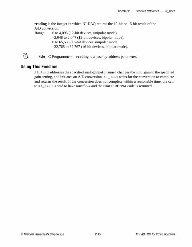
Chapter 2 Function Reference — AI_Read
© National Instruments Corporation 2-15 NI-DAQ FRM for PC Compatibles
reading is the integer in which NI-DAQ returns the 12-bit or 16-bit result of the A/D conversion.Range: 0 to 4,095 (12-bit devices, unipolar mode).
–2,048 to 2,047 (12-bit devices, bipolar mode).0 to 65,535 (16-bit devices, unipolar mode).–32,768 to 32,767 (16-bit devices, bipolar mode).
Note C Programmers—reading is a pass-by-address parameter.
Using This FunctionAI_Read addresses the specified analog input channel, changes the input gain to the specified gain setting, and initiates an A/D conversion. AI_Read waits for the conversion to complete and returns the result. If the conversion does not complete within a reasonable time, the call to AI_Read is said to have timed out and the timeOutError code is returned.

Chapter 2 Function Reference — AI_Read_Scan
NI-DAQ FRM for PC Compatibles 2-16 www.natinst.com
AI_Read_Scan
Formatstatus = AI_Read_Scan (deviceNumber, reading)
PurposeReturns readings for all analog input channels selected by SCAN_Setup (E Series devices only, with or without the SC-2040 accessory).
ParametersInput
Output
Parameter Discussionreading is an array of readings from each sampled analog input channel. The length of the reading array is equal to the number of channels selected in the SCAN_Setup numChans parameter. Range of elements in reading depends on your device A/D converter resolution and the unipolar/bipolar selection you made make for a given channel.
Using This FunctionAI_Read_Scan samples the analog input channels selected by SCAN_Setup, at half the maximum rate permitted by your data acquisition hardware.
You must use the SCAN_Setup function prior to invoking this function.
You cannot use external signals to control A/D conversion timing and use this function at the same time.
Name Type Description
deviceNumber i16 assigned by configuration utility
Name Type Description
reading [i16] readings from each sampled analog input channel
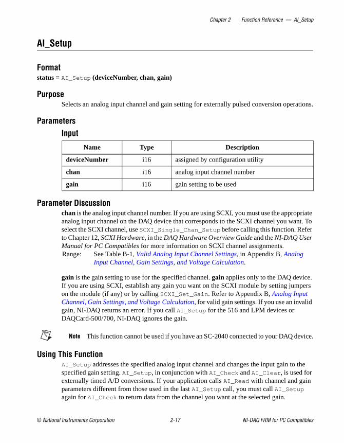
Chapter 2 Function Reference — AI_Setup
© National Instruments Corporation 2-17 NI-DAQ FRM for PC Compatibles
AI_Setup
Formatstatus = AI_Setup (deviceNumber, chan, gain)
PurposeSelects an analog input channel and gain setting for externally pulsed conversion operations.
ParametersInput
Parameter Discussionchan is the analog input channel number. If you are using SCXI, you must use the appropriate analog input channel on the DAQ device that corresponds to the SCXI channel you want. To select the SCXI channel, use SCXI_Single_Chan_Setup before calling this function. Refer to Chapter 12, SCXI Hardware, in the DAQ Hardware Overview Guide and the NI-DAQ User Manual for PC Compatibles for more information on SCXI channel assignments.Range: See Table B-1, Valid Analog Input Channel Settings, in Appendix B, Analog
Input Channel, Gain Settings, and Voltage Calculation.
gain is the gain setting to use for the specified channel. gain applies only to the DAQ device. If you are using SCXI, establish any gain you want on the SCXI module by setting jumpers on the module (if any) or by calling SCXI_Set_Gain . Refer to Appendix B, Analog Input Channel, Gain Settings, and Voltage Calculation, for valid gain settings. If you use an invalid gain, NI-DAQ returns an error. If you call AI_Setup for the 516 and LPM devices or DAQCard-500/700, NI-DAQ ignores the gain.
Note This function cannot be used if you have an SC-2040 connected to your DAQ device.
Using This FunctionAI_Setup addresses the specified analog input channel and changes the input gain to the specified gain setting. AI_Setup , in conjunction with AI_Check and AI_Clear , is used for externally timed A/D conversions. If your application calls AI_Read with channel and gain parameters different from those used in the last AI_Setup call, you must call AI_Setup again for AI_Check to return data from the channel you want at the selected gain.
Name Type Description
deviceNumber i16 assigned by configuration utility
chan i16 analog input channel number
gain i16 gain setting to be used

Chapter 2 Function Reference — AI_VRead
NI-DAQ FRM for PC Compatibles 2-18 www.natinst.com
AI_VRead
Formatstatus = AI_VRead (deviceNumber, chan, gain, voltage)
PurposeReads an analog input channel (initiates an A/D conversion on an analog input channel) and returns the result scaled to a voltage in units of volts.
ParametersInput
Output
Parameter Discussionchan is the analog input channel number.Range: See Table B-1, Valid Analog Input Channel Settings, in Appendix B, Analog
Input Channel, Gain Settings, and Voltage Calculation.
gain is the gain setting to be used for the specified channel. Refer to Appendix B, Analog Input Channel, Gain Settings, and Voltage Calculation, for valid gain settings. If you use an invalid gain, NI-DAQ returns an error. If you call AI_VRead for the 516 and LPM devices or DAQCard-500/700, NI-DAQ ignores the gain.
voltage is the floating-point variable in which NI-DAQ returns the measured voltage, scaled to units of volts.
Note C Programmers—voltage is a pass-by-address parameter.
Name Type Description
deviceNumber i16 assigned by configuration utility
chan i16 analog input channel number
gain i16 gain setting to be used for the specified channel
Name Type Description
voltage *f64 the measured voltage returned, scaled to units of volts

Chapter 2 Function Reference — AI_VRead
© National Instruments Corporation 2-19 NI-DAQ FRM for PC Compatibles
Using This FunctionAI_VRead addresses the specified analog input channel, changes the input gain to the specified gain setting, and initiates an A/D conversion. AI_VRead waits for the conversion to complete and then scales and returns the result. If the conversion does not complete within a reasonable time, the call to AI_VRead is said to have timed out and NI-DAQ returns the timeOutError code.
When you use SCXI as a front end for analog input to an MIO or AI device, 1200 Series device, LPM device, or DAQCard-700, it is not advisable to use the AI_VRead function because that function does not take into account the gain of the SCXI module when scaling the data. Use the AI_Read function to get unscaled data, and then call the SCXI_Scale function.
When you have an SC-2040 accessory connected to an E Series device, this function takes both the onboard gains and the gains on SC-2040 into account while scaling the data. When you have an SC-2043-SG accessory connected to your DAQ device, this function takes both the onboard gains and the SC-2043-SG fixed gain of 10 into account while scaling the data.
When you have any SCC accessories connected to an E Series device, this function takes both the onboard gains and the SCC gains into account while scaling the data.

Chapter 2 Function Reference — AI_VRead_Scan
NI-DAQ FRM for PC Compatibles 2-20 www.natinst.com
AI_VRead_Scan
Formatstatus = AI_VRead_Scan (deviceNumber, reading)
PurposeReturns readings in volts for all analog input channels selected by SCAN_Setup (E Series devices only with or without the SC-2040 accessory).
ParametersInput
Output
Parameter Discussionreading is an array of readings from each sampled analog input channel. The length of the reading array is equal to the number of channels selected in the SCAN_Setup numChans parameter. NI-DAQ uses values you have specified in SCAN_Setup through the gains parameter for computing voltages. If you have attached an SC-2040 or SC-2043-SG to your DAQ device, NI-DAQ also uses values you have specified in SC_2040_Config (through thesc2040gain parameter) or Set_DAQ_Device_Info (a fixed gain of 10) for computing voltages.
If you have SCC modules connected, NI-DAQ also uses the SCC module gain for computing voltages.
Using This FunctionAI_VRead_Scan samples the analog input channels selected by SCAN_Setup, at half the maximum rate your DAQ hardware permits.You must use the SCAN_Setup function prior to invoking this function.
You cannot use external signals to control A/D conversion timing and use this function at the same time.
Name Type Description
deviceNumber i16 assigned by configuration utility
Name Type Description
reading [f64] voltage readings from each sampled analog input channel

Chapter 2 Function Reference — AI_VScale
© National Instruments Corporation 2-21 NI-DAQ FRM for PC Compatibles
AI_VScale
Formatstatus = AI_VScale (deviceNumber, chan, gain, gainAdjust, offset, reading, voltage)
PurposeConverts the binary result from an AI_Read call to the actual input voltage.
ParametersInput
Output
Parameter Discussionchan is the onboard channel or AMUX channel on which NI-DAQ took the binary reading using AI_Read . For devices other than the E Series devices, this parameter is ignored because the scaling calculation is the same for all of the channels. However, National Instruments recommends you to pass the correct channel number.
gain is the gain setting that you used to take the analog input reading. If you used SCXI to take the reading, this gain parameter should be the product of the gain on the SCXI module channel and the gain that the DAQ device used. Refer to Appendix B, Analog Input Channel, Gain Settings, and Voltage Calculation, for valid gain settings. Use of invalid gain settings causes NI-DAQ to return an error unless you are using SCXI. If you call AI_VScale for the 516 and LPM devices or DAQCard-500/700, NI-DAQ ignores the gain unless you are using SCXI.
Name Type Description
deviceNumber i16 assigned by configuration utility
chan i16 channel on which binary reading was taken
gain i16 gain setting used to take the reading
gainAdjust f64 multiplying factor to adjust gain
offset f64 binary offset present in reading
reading i16 result of the A/D conversion
Name Type Description
voltage *f64 computed floating-point voltage

Chapter 2 Function Reference — AI_VScale
NI-DAQ FRM for PC Compatibles 2-22 www.natinst.com
gainAdjust is the multiplying factor to adjust the gain. Refer to Appendix B, Analog Input Channel, Gain Settings, and Voltage Calculation, for the procedure for determining gainAdjust. If you do not want to do any gain adjustment—for example, use the ideal gain as specified by the gain parameter—set gainAdjust to 1.
offset is the binary offset that needs to be subtracted from the reading. Refer to Appendix B, Analog Input Channel, Gain Settings, and Voltage Calculation, for the procedure for determining offset. If you do not want to do any offset compensation, set offset to 0.
reading is the result of the A/D conversion returned by AI_Read .
voltage is the variable in which NI-DAQ returns the input voltage converted from reading.
Note C Programmers—voltage is a pass-by-address parameter.
Using This FunctionRefer to Appendix B, Analog Input Channel, Gain Settings, and Voltage Calculation, for the formula AI_VScale uses to calculate voltage from reading.
If your device polarity and range settings differ from the default settings shown in the Init_DA_Brds function, be sure to call AI_Configure to inform the driver of the correct polarity and range before using this function.

Chapter 2 Function Reference — Align_DMA_Buffer
© National Instruments Corporation 2-23 NI-DAQ FRM for PC Compatibles
Align_DMA_Buffer
Formatstatus = Align_DMA_Buffer (deviceNumber, resource, buffer, count, bufferSize, alignIndex)
PurposeAligns the data in a DMA buffer to avoid crossing a physical page boundary. This function is for use with DMA waveform generation and digital I/O pattern generation (AT-DIO-32F only).
ParametersInput
Input/Output
Output
Parameter Discussionresource represents the DAC channel (for waveform generation) or the digital input or output group (for pattern generation) for which NI-DAQ uses the buffer.
0: DAC channel 0.1: DAC channel 1.2: DAC channels 0 and 1.
11: DIG group 1 (group size of 2).
Name Type Description
deviceNumber i16 assigned by configuration utility
resource i16 represents the DAC channel or the digital input or output group
count u32 number of data samples
bufferSize u32 actual size of buffer
Name Type Description
buffer [i16] conversion samples returned
Name Type Description
alignIndex *u32 offset into the array of the first data sample

Chapter 2 Function Reference — Align_DMA_Buffer
NI-DAQ FRM for PC Compatibles 2-24 www.natinst.com
12: DIG group 2 (group size of 2).13: DIG group 1 (group size of 4).
buffer is the integer array of samples NI-DAQ uses in the waveform or pattern generation. The actual size of buffer should be larger than the number of samples to make room for possible alignment. If the actual size of the buffer is not big enough for alignment, the function returns a memAlignmentError . For Windows applications running in real or standard mode, a bufferSize of 2*count guarantees that there is enough room for alignment.
count is the number of data samples contained in buffer.Range: 3 through 232– 1.
bufferSize is the actual size of buffer.Range: count through 232–1.
alignIndex is the variable in which NI-DAQ returns the offset into the array of the first data sample. If NI-DAQ did not have to align the buffer, NI-DAQ returns alignIndex as 0, indicating that the data is still located at the beginning of the buffer. If NI-DAQ aligned the buffer to avoid a page boundary, alignIndex is a value other than 0, and the first data sample is located at buffer [alignIndex] (if your array is zero based). If you use digital input with an aligned buffer, NI-DAQ stores the data in the buffer beginning at alignIndex.
Note C Programmers—alignIndex is a pass-by-address parameter.
Using This FunctionUse Align_DMA_Buffer to avoid the negative effects of page boundaries in the data buffer on AT bus machines for the following cases:
• DMA waveform generation at close to maximum speed.
• Digital I/O pattern generation at close to maximum speed.
• Interleaved DMA waveform generation at any speed.
• 32-bit digital I/O pattern generation at any speed.
The possibility of a page boundary occurring in the data buffer increases with the size of the buffer. When a page boundary occurs in the data buffer, NI-DAQ must reprogram the DMA controller before NI-DAQ can transfer the next data sample. The extra time needed to do the reprogramming increases the minimum update interval (thus decreasing the maximum update rate).
A page boundary in an interleaved DMA waveform buffer or a buffer that is to be used for 32-bit digital pattern generation can cause unpredictable results, regardless of your operating speed. To avoid this problem, you should always use Align_DMA_Buffer with interleaved DMA waveform generation (indicated by resource = 2) and 32-bit digital pattern generation (indicated by resource = 13). In these two cases, Align_DMA_Buffer first attempts to align

Chapter 2 Function Reference — Align_DMA_Buffer
© National Instruments Corporation 2-25 NI-DAQ FRM for PC Compatibles
the buffer so that the data completely avoids a page boundary. If bufferSize is not big enough for complete alignment, the function attempts to partially align the data to ensure that a page boundary does not cause unpredictable results. Partial alignment is possible if bufferSize ≥ count + 1. If neither form of alignment is possible, the function returns an error. If Align_DMA_Buffer partially aligned the data, the function returns a memPageError warning indicating that a page boundary is still in the data.
Note Physical DMA page boundaries do not exist on EISA bus computers. However, page boundaries can be introduced on these computers as a side effect of Windows 386 Enhanced mode and the Windows NT virtual memory management system. This happens when a buffer is locked into physical memory in preparation for a DAQ operation. If the memory manager cannot find a contiguous space large enough, it fragments the buffer, placing pieces of it here and there in physical memory. This type of page boundary only affects the performance on an AT bus computer. NI-DAQ uses the DMA chaining feature available on EISA computers to chain across page boundaries, thus avoiding the delay involved in DMA programming.
Call Align_DMA_Buffer after your application has loaded buffer with the data samples (for waveform generation or digital output) and before calling WFM_Op, WFM_Load, DIG_Block_In , or DIG_Block_Out . You should pass the aligned buffer to the waveform generation and pattern generation functions the same way you would an unaligned buffer. The count parameter in the waveform generation or pattern generation function call should be the same as the count parameter passed to Align_DMA_Buffer , not bufferSize.
If you want to access the data in buffer after calling Align_DMA_Buffer , access the data starting at buffer [alignIndex] (if your array is zero based).
After using an aligned buffer for waveform generation or pattern generation, NI-DAQ unaligns the data. After the buffer has been unaligned, the first data sample is at offset zero of the buffer again. If you want to use the buffer for waveform generation or pattern generation again after it has been unaligned, you must make another call to Align_DMA_Buffer before calling WFM_Op, WFM_Load, DIG_Block_In , or DIG_Block_Out .
See Waveform Generation Application Hints and Digital I/O Application Hints in Chapter 3, Software Overview, of the NI-DAQ User Manual for PC Compatibles for more information on the use of Align_DMA_Buffer . See Chapter 4, DMA and Programmed I/O Performance Limitations, of the NI-DAQ User Manual for PC Compatibles for a discussion of DMA page boundaries and special run-time considerations.

Chapter 2 Function Reference — AO_Calibrate
NI-DAQ FRM for PC Compatibles 2-26 www.natinst.com
AO_Calibrate
Formatstatus = AO_Calibrate (deviceNumber, operation, EEPROMloc)
PurposeLoads a set of calibration constants into the calibration DACs or copies a set of calibration constants from one of four EEPROM areas to EEPROM area 1. You can load an existing set of calibration constants into the calibration DACs from a storage area in the onboard EEPROM. You can copy EEPROM storage areas 2 through 5 (EEPROM area 5 contains the factory calibration constants) to storage area 1. NI-DAQ automatically loads the calibration constants stored in EEPROM area 1 the first time a function pertaining to the AT-AO-6/10 is called. The 6704 devices automatically load the calibration constants stored in EEPROM area 1 on power-up.
Note Use the calibration utility provided with the AT-AO-6/10 to perform a calibration procedure. Refer to the calibration chapter in the AT-AO-6/10 User Manual for more information regarding the calibration procedure.
ParametersInput
Parameter Discussionoperation determines the operation to be performed.
1: Load calibration constants from EEPROMloc.2: Copy calibration constants from EEPROMloc to EEPROM user calibration
area 1.
EEPROMloc selects the storage location in the onboard EEPROM to be used. You can use different sets of calibration constants to compensate for configuration or environmental changes.
1: User calibration area 1.2: User calibration area 2.3: User calibration area 3.
Name Type Description
deviceNumber i16 assigned by configuration utility
operation i16 operation to be performed
EEPROMloc i16 storage location in the onboard EEPROM

Chapter 2 Function Reference — AO_Calibrate
© National Instruments Corporation 2-27 NI-DAQ FRM for PC Compatibles
4: User calibration area 4.5: Factory calibration area.
Note Locations 2 through 4 are not available for the 6704 family.
Using This FunctionWhen NI-DAQ initializes the AT-AO-6/10, the DAC calibration constants stored in EEPROMloc 1 (user calibration area 1) provide the gain and offset values used to ensure proper device operation. In other words, Init_DA_Brds performs the equivalent of calling AO_Calibrate with operation set to 1 and EEPROMloc set to 1. When the AT-AO-6/10 leaves the factory, EEPROMloc 1 contains a copy of the calibration constants stored in EEPROMloc 5, the factory area.
A calibration procedure performed in bipolar mode is not valid for unipolar and vice versa. See the calibration chapter of the AT-AO-6/10 User Manual for more information regarding calibrating the device.
The 6704 devices automatically load the calibration constants stored in EEPROMloc1 at power-up. EEPROMloc 5 contains the factory calibration values. When a 6704 device leaves the factory, EEPROMloc 1 contains a copy of the factory calibration constants stored in EEPROMloc 5. To save a new set of calibration constants to the EEPROM, call AO_Calibrate with operation set to 2. See the calibration section of the PCI/PXI-6704 User Manual for more information regarding calibrating this device.

Chapter 2 Function Reference — AO_Change_Parameter
NI-DAQ FRM for PC Compatibles 2-28 www.natinst.com
AO_Change_Parameter
Formatstatus = AO_Change_Parameter (deviceNumber, channel, paramID, paramValue)
PurposeSelects a specific parameter setting for the analog output section of the device or an analog output channel. You can select parameters related to analog output not listed here through the AO_Configure function.
ParametersInput
Parameter DiscussionLegal ranges for paramID and paramValue are given in terms of constants defined in a header file. The header file you should use depends on the language you are using:
• C programmers—NIDAQCNS.H (DATAACQ.H for LabWindows/CVI)
• BASIC programmers—NIDAQCNS.INC (Visual Basic for Windows programmers should refer to the Programming Language Considerations in Chapter 1, Using the NI-DAQ Functions, for more information.)
• Pascal programmers—NIDAQCNS.PAS
Legal values for channel depend on the type of device you are using; analog output channels are labeled 0 through n–1, where n is the number of analog output channels on your device. You can set channel to –1 to indicate that you want the same parameter selection for all channels. You must set channel to –1 to change a parameter you cannot change on per channel basis.
Name Type Description
deviceNumber i16 assigned by configuration utility
channel i16 number of channel you want to configure; you can use –1 to indicate all channels
paramID u32 identification of the parameter you want to change
paramValue u32 new value for the parameter specified by paramID

Chapter 2 Function Reference — AO_Change_Parameter
© National Instruments Corporation 2-29 NI-DAQ FRM for PC Compatibles
Legal values for paramValue depend on paramID . The following paragraphs list features you can configure along with legal values for paramID with explanations and corresponding legal values for paramValue.
ReglitchingEvery time you change the state of your DAC, a very small glitch is generated in the signal generated by the DAC. When reglitching is turned off, glitch size depends on the binary patterns that are written into the DAC; the glitch is largest when the most significant bit in the pattern changes (when the waveform crosses the midrange of the DAC); it is smaller in other cases. When reglitching is turned on, the glitch size is much less dependent on the bit pattern.
To change the reglitching parameter, set paramID to ND_REGLITCH.
If you are not concerned about this, you are likely to be satisfied by the default values NI-DAQ selects for you if you do not call this function. The following table lists devices on which you can change this parameter.
Voltage or Current OutputSome devices require separate calibration constants for voltage and current outputs. Setting the output type to voltage or current for these devices causes the driver to use the correct calibration constants and to interpret the input data correctly in AO_VWrite . To change the output type, set paramID to ND_OUTPUT_TYPE.
Table 2-3. Reglitching Parameters for Permissible Devices
Device TypePer Channel
Selection PossibleLegal Range for
paramValueDefault Setting for
paramValue
AT-MIO-16E-1 AT-MIO-16E-2 AT-MIO-64E-3 NEC-MIO-16E-4PCI-MIO-16E-1VXI-MIO-64E-1VXI-MIO-64XE-10671X devices
Yes ND_OFF and ND_ON
ND_OFF
Table 2-4. Voltage or Current Output Parameters
Device TypePer Channel
Selection PossibleLegal Range for
paramValueDefault Setting for
paramValue
PC-AO-2DCDAQCard-AO-2DCVXI-AO-48XDC
Yes ND_CURRENT_OUTPUT and ND_VOLTAGE_OUTPUT
ND_VOLTAGE_OUTPUT

Chapter 2 Function Reference — AO_Change_Parameter
NI-DAQ FRM for PC Compatibles 2-30 www.natinst.com
For the VXI-AO-48XDC device, the paramID of ND_OUTPUT_TYPE is used in conjunction with the channel value to select the analog output channel to be affected. To select a voltage channel, set the paramValue to ND_VOLTAGE. To select a current channel, set the paramValue to ND_CURRENT.
FIFO Transfer ConditionYou can specify the condition that causes more data to be transferred from the waveform buffer into the analog output FIFO. NI-DAQ selects a default setting for you, in order to achieve maximum performance. However, by changing this setting, you can force the FIFO to remain as full as possible, or effectively disable, or reduce the size of the FIFO.
For example, to reduce the FIFO lag effect (the amount of time it takes data to come out of the FIFO after being transferred into the FIFO), you can change the FIFO transfer condition to FIFO empty. Notice that reducing the effective FIFO size can also reduce the maximum sustainable update rate.
To change the FIFO transfer condition, set paramID to ND_DATA_TRANSFER_CONDITION, and set paramValue to one of the values shown in Table 2-5.
Set channel to one of the channel numbers in your waveform group. For example, if you have configured group 1 to contain channels 0 and 1, you can set channel to 0 or 1.
Note The option to set the channel to one of the channel numbers in your waveform group is valid only for PCI/PXI/1394 E Series and 671X devices.
When using PCI/PXI/1394 E Series or 671X devices with DMA (default data transfer condition), the device has an effective FIFO size 32 samples larger than the FIFO size specified for the board. This is due to a 32-sample FIFO on the miniMITE, the onboard DMA controller used for DMA transfers.
Table 2-5. Parameter Values for FIFO Transfer Conditions
Transfer Condition NI-DAQ Constant
FIFO not full ND_FIFO_NOT_FULL
FIFO half-full or less ND_FIFO_HALF_FULL_OR_LESS
FIFO empty ND_FIFO_EMPTY
FIFO half-full or less until full (DMA only)
ND_FIFO_HALF_FULL_OR_LESS_UNTIL_FULL

Chapter 2 Function Reference — AO_Change_Parameter
© National Instruments Corporation 2-31 NI-DAQ FRM for PC Compatibles
FIFO Transfer CountThe FIFO transfer count specifies the number of samples to be transferred from the waveform buffer into the analog output FIFO when FIFO requests are generated. This option is for use in conjunction with the FIFO transfer condition, as described in the previous section.
AO_Change_Parameter should be called once to set the FIFO transfer condition, and can optionally be called again to specify the FIFO transfer count. If you do not specify the FIFO transfer count, NI-DAQ chooses an appropriate value for you.
The value of FIFO transfer count is used during interrupt-driven waveform generation but is ignored during DMA-driven waveform generation. When you use DMA, DMA requests are generated as long as the transfer condition is true.
Table 2-6 contains the default values that are used if you do not specify FIFO transfer count, in addition to the valid values that you can set.
For example, if you choose the FIFO empty transfer condition and set the transfer count to 10, each time the board is interrupted with a FIFO empty interrupt, NI-DAQ transfers 10 samples from the user buffer into the analog output FIFO. Although this does not improve the maximum sustainable update rate, it reduces the number of interrupts, and reduces the FIFO lag effect to a maximum of 10 samples.
If you choose the FIFO half full or less transfer condition and set the transfer count to 100 on a board with a 2,048-sample FIFO, the FIFO fills with a maximum of 1,124 samples (half the FIFO plus 100 samples). Each time the number of samples in the FIFO falls to less than 1,024, another interrupt is generated, at which time 100 samples are transferred from the waveform buffer to the FIFO.
To change the FIFO transfer count, set paramID to ND_FIFO_TRANSFER_COUNT and use paramValue to pass in a 32-bit integer.
Set channel to one of the channel numbers in your waveform group. For example, if you have configured group 1 to contain channels 0 and 1, you can set channel to 0 or 1.
Table 2-6. Default Values for FIFO Transfer Condition
Transfer Condition Default Transfer Count Valid Input Values
FIFO not full 1 1
FIFO half-full or less half-FIFO size 1—half-FIFO size
FIFO empty 1 1—FIFO size
FIFO half-full or less until full (DMA only)
FIFO transfer count cannot be specified for this transfer condition
N/A

Chapter 2 Function Reference — AO_Change_Parameter
NI-DAQ FRM for PC Compatibles 2-32 www.natinst.com
Note The option to set the channel to one of the channel numbers in your waveform group is valid only for PCI/PXI/1394 E Series and 671X devices.
Ground DAC ReferenceYou can ground the reference that the analog output channels use, which causes the output voltage to remain at 0 V, regardless of the value you write to the channel.
To change the grounding of the DAC Reference, set paramID to ND_GROUND_DAC_REFERENCE, and set paramValue to either ND_YES, or ND_NO. The effect is immediate. Also, grounding the DAC reference on one channel has the effect of grounding it for both channels, so you can specify either 0 or 1 for channel number.
Note The option to set the channel to one of the channel numbers in your waveform group is valid only for PCI/PXI/1394 E Series and 671X devices.
Output EnableOn some of the devices, you can disable the output even when the waveform generation is in progress. You can use this feature to bring the output to a known level at any time.
To change the output enable setting, set paramID to ND_OUTPUT_ENABLE.
Output Attenuation Some devices have attenuators after the final amplifier stage. By attenuating the output signal, you do not lose any dynamic range of the signal; that is, you do not lose any bits from the digital representation of the signal, because the attenuation is done after the DAC and not before it.
Attenuation (in mdB) = –[20 log10 (Vo/Vi)]*1000
Vo = The voltage level that you want for the output signal.Vi = The input voltage level.
The 4451 and 4551 devices have three levels of attenuation providing voltage ranges of –10 to + 10 V, –1 to +1 V, and –100 to +100 mV.
Table 2-7. Parameter Setting Information for Output Enable
Device TypePer Channel
Selection PossibleLegal Range
for paramValueDefault Setting for paramValue
4451, 4453, and 4551 devices
Yes ND_YES and ND_NO
ND_NO

Chapter 2 Function Reference — AO_Change_Parameter
© National Instruments Corporation 2-33 NI-DAQ FRM for PC Compatibles
To change the output attenuation setting set paramID to ND_ATTENUATION. You can change the attenuation at any time.
Note The values are set up in millidecibels.
End of Buffer InterruptsOn PCI/PXI/1394 E Series and 671X boards that use the PCI-MITE for DMA transfers, NI-DAQ causes the PCI-MITE to generate an interrupt after a full buffer has been transferred from host memory to the DAQ device. With one-shot operations, where the buffer is only output once, or even during continuous operations where the buffer is very large, these interrupts place very little burden on the system. However, when outputting a large number of iterations with small buffers or at high speeds, these interrupts can affect overall system performance.
These interrupts are generated so that NI-DAQ will read the state of the DMA controller and track the number of iterations and the number of points transferred since the beginning of the operation. The PCI-MITE has a 32-bit counter that counts bytes transferred. The only drawback in turning off these interrupts is that NI-DAQ might not have a chance to detect an overflow of the counter. For example, when generating a waveform on one channel at 1 Msamples/s, the counter will overflow in 36 minutes. If you disable end-of-buffer interrupts and do not query NI-DAQ for status information before the counter overflows, NI-DAQ will not be able to take the overflow into account, and the status information returned could be incorrect.
To enable/disable end-of-buffer interrupts, set paramID to ND_LINK_COMPLETE_INTERRUPTS and set paramValue to either ND_ON or ND_OFF. You may specify any channel in the waveform group, and the setting will apply to all channels in the group.
Note This option is valid only for PCI/CPCI/PXI/1394 E Series and 671X devices.
Table 2-8. Parameter Setting Information for Output Attenuation
Device TypePer Channel
Selection PossibleLegal Range
for paramValueDefault Setting for paramValue
4451, 4453, and 4551 devices Yes 0, 20,000, 40,000 0

Chapter 2 Function Reference — AO_Change_Parameter
NI-DAQ FRM for PC Compatibles 2-34 www.natinst.com
Memory Transfer WidthWhen doing waveform generation on PCI/PXI/1394 E Series boards that use the PCI-MITE for DMA transfers, NI-DAQ transfers data from host memory to the DAQ device 16 bits at a time. This allows for the finest level of control and is necessary to properly support features like oldDataStop and partialTransferStop (see the NI-DAQ function WFM_DB_Config).
It is also possible to transfer data from host memory to the DAQ device 32 bits at a time, which requires fewer PCI bus cycles so that the DAQ device functions more effectively with the PCI bus. The only drawback is that when using oldDataStop and partialTransferStop , the waveform may stop one sample earlier than you would otherwise expect.
To set the memory transfer width, set paramID to ND_MEMORY_TRANSFER_WIDTH and set paramValue to either 16 or 32. You may specify any channel in the waveform group, and the setting will apply to all channels in the group.
Note This option is valid only for PCI/CPCI/PXI/1394 E Series devices. For 61XX and 671X devices, only even-sized buffers are allowed, and the memory transfer width is always 32 bits.

Chapter 2 Function Reference — AO_Configure
© National Instruments Corporation 2-35 NI-DAQ FRM for PC Compatibles
AO_Configure
Formatstatus = AO_Configure (deviceNumber, chan, outputPolarity, intOrExtRef, refVoltage,
updateMode)
PurposeInforms NI-DAQ of the output range and polarity selected for each analog output channel on the device and indicates the update mode of the DACs. If you have recorded an analog output configuration that is not a default through Measurement & Automation Explorer, you do not need to use AO_Configure because NI-DAQ uses the settings recorded by Measurement & Automation Explorer. If you have a software-configurable device, you can use AO_Configure to change the analog output configuration on the fly.
Caution For the AT-AO-6/10, NI-DAQ records the configuration information for output polarity and update mode in channel pairs. A call to AO_Configure records the same output polarity and update mode selections for both channels in a pair.
ParametersInput
Parameter Discussionchan is the analog output channel number.Range: 0 or 1 for the AO-2DC, Lab and 1200 Series analog output devices, and
MIO devices.0 through 5 for the AT-AO-6.0 through 9 for the AT-AO-10.0 through 47 for the VXI-AO-48XDC.0 through 15 for the 6704 device voltage channels.16 through 31 for the 6704 current channels.
Name Type Description
deviceNumber i16 assigned by configuration utility
chan i16 analog output channel number
outputPolarity i16 unipolar or bipolar
intOrExtRef i16 reference source
refVoltage f64 voltage reference value
updateMode i16 when to update the DACs

Chapter 2 Function Reference — AO_Configure
NI-DAQ FRM for PC Compatibles 2-36 www.natinst.com
0 through 3 for the PCI-6711.0 through 7 for the PCI-6713.
outputPolarity indicates whether the analog output channel is configured for unipolar or bipolar operation.
For the AT-AO-6/10 and MIO devices (except the MIO-16XE-50 devices):0: Bipolar operation (default setting, output range is from –refVoltage to
+refVoltage).1: Unipolar operation (output range is from 0 to +refVoltage).
For the Lab and 1200 Series analog output devices:0: Bipolar operation (default setting, output range is from –5 to +5 V).1: Unipolar operation (output range is from 0 to +10 V).
For the 671X and MIO-16XE-50 devices:0: Bipolar operation (output range is from –10 to +10 V).
For the AO-2DC devices:0: Bipolar operation (output range is from –5 to +5 V).1: Unipolar operation (default setting, output range is from 0 to +10 V
or 0 to 20 mA).
For the 6704 devices and the VXI-AO-48XDC:0: Bipolar operation (voltage only; output range is from –10.24 to +10.24 V).1: Unipolar operation (current only; output range is from 0 to 20.47 mA).
intOrExtRef indicates the source of voltage reference.0: Internal reference.1: External reference.
The AT-AO-6/10, 12-bit MIO, and 6052E devices support external analog output voltage references. The other 16-bit E Series and 671X devices do not support external references.
For the 6704 devices, only internal reference is supported.
refVoltage is the analog output channel voltage reference value. You can configure each channel to use an internal reference of +10 V (the default) or an external reference. Although each pair of channels is served by a single external reference connection, the configuration of the external reference operates on a per channel basis. Therefore, it is possible to have one channel in a pair internally referenced and the other channel in the same pair externally referenced.Range: –10 to +10 V.

Chapter 2 Function Reference — AO_Configure
© National Instruments Corporation 2-37 NI-DAQ FRM for PC Compatibles
If you make a reference voltage connection, you must assign refVoltage the value of the external reference voltage in a call to AO_Configure for the AO_VWrite and AO_VScale functions to operate properly. For devices that have no external reference pin, the output range is determined by outputPolarity , and NI-DAQ ignores this parameter.
updateMode indicates whether an analog output channel is updated when written to:0: Updated when written to (default setting).1: Not updated when written to, but updated later after a call to AO_Update
(later internal update mode).2: Not updated when written to, but updated later upon application of an active low
pulse. You should apply this pulse to the following:
• EXTUPDATE pin for the AT-AO-6/10 and Lab and 1200 Series analog output devices (later external update mode).
• PFI5 pin for the E Series and 671X devices. To alter the pin and polarity selections you make with this function, for an E Series or 671X device, you can call Select_Signal with signal = ND_OUT_UPDATE after you call AO_Configure .
Note This mode is not valid for the VXI-AO-48XDC or the 6704 devices.
Using This FunctionAO_Configure stores information about the analog output channel on the specified device in the configuration table for the analog channel. For the AT-AO-6/10, the outputPolarity and updateMode information is stored for channel pairs. For example, analog output channels 0 and 1 are grouped in a channel pair, and a call to AO_Configure for channel 0 records the outputPolarity and updateMode for both channels 0 and 1. Likewise, a call to AO_Configure for channel 1 records the outputPolarity and updateMode for both channels 0 and 1. The AT-AO-6/10 channel pairs are as follows:
AT-AO-6/10 channel pairs:
• Channels 0 and 1.
• Channels 2 and 3.
• Channels 4 and 5.
• Channels 6 and 7 (AT-AO-10 only).
• Channels 8 and 9 (AT-AO-10 only).

Chapter 2 Function Reference — AO_Configure
NI-DAQ FRM for PC Compatibles 2-38 www.natinst.com
AO_Configure stores information about the analog output channel on the specified board in the configuration table for the analog channel. The analog output channel configuration table defaults tables default to the following:
• MIO device, 671X device, and AT-AO-6/10:
outputPolarity = 0: Bipolar.refVoltage = 10 V.updateMode = 0: Update when written to.
• Lab and 1200 Series analog output devices:
outputPolarity = 0: Bipolar (–5 to +5 V).updateMode = 0: Updated when written to.
• 6704 device voltage channels and the VXI-AO-48XDC:
outputPolarity = 0: Bipolar (–10.24 to +10.24 V).updateMode = 0: Updated when written to.
• 6704 device current channels:
outputPolarity = 1: Unipolar (0 to 20.47 mA).updateMode = 0: Updated when written to.
If you configure an output channel for later internal update mode (updateMode = 1), you can configure no other output channels for later external update mode (updateMode= 2). Likewise, if you configure an output channel for later external update mode, you can configure no other output channels for later internal update mode.
If the physical configuration (the jumpered settings) of the analog output channels on your device differs from the default setting, you must call AO_Configure with the true configuration information for the remaining analog output functions to operate properly.
Note The AT-AO-6/10 allows you to physically configure each analog output channel (the jumper setting) for bipolar or unipolar operation. To ensure proper operation, configure both channels in a channel pair the same way.
On the E Series devices (except MIO-16XE-50 devices), the calibration constants used for analog output change depending on the polarity of the analog output channels. NI-DAQ always ensures that the calibration constants in use match the current polarity of the channels.
The actual loading of calibration constants takes place when you call an AO or WFM function. See the Calibrate_E_Series function description for information about calibration constant loading on the E Series devices.

Chapter 2 Function Reference — AO_Update
© National Instruments Corporation 2-39 NI-DAQ FRM for PC Compatibles
AO_Update
Formatstatus = AO_Update (deviceNumber)
PurposeUpdates analog output channels on the specified device to new voltage values when the later internal update mode is enabled by a previous call to AO_Configure .
ParametersInput
Using This FunctionAO_Update issues an update pulse to all analog output channels on the specified device. All analog output channel voltages then simultaneously change to the last value written.
Name Type Description
deviceNumber i16 assigned by configuration utility

Chapter 2 Function Reference — AO_VScale
NI-DAQ FRM for PC Compatibles 2-40 www.natinst.com
AO_VScale
Formatstatus = AO_VScale (deviceNumber, chan, voltage, binVal)
PurposeScales a voltage to a binary value that, when written to one of the analog output channels, produces the specified voltage.
ParametersInput
Output
Parameter Discussionchan is the analog output channel number. Range: 0 or 1 for the Lab and 1200 Series analog output devices, and MIO devices.
0 through 5 for AT-AO-6.0 through 10 for AT-AO-10.0 through 47 for the VXI-AO-48XDC.0 through 15 for the 6704 device voltage channels.16 through 31 for the 6704 device current channels.0 through 3 for the PCI-6711.0 through 7 for the PCI-6713.
Note C Programmers—binVal is a pass-by-address parameter.
Name Type Description
deviceNumber i16 assigned by configuration utility
chan i16 analog output channel number
voltage f64 voltage, in volts, to be converted to a binary value
Name Type Description
binVal *i16 converted binary value returned

Chapter 2 Function Reference — AO_VScale
© National Instruments Corporation 2-41 NI-DAQ FRM for PC Compatibles
Using This FunctionUsing the following formula, AO_VScale calculates the binary value to be written to the specified analog output channel to generate an output voltage corresponding to voltage.
binVal = (voltage/refVoltage) * maxBinVal
where values of refVoltage and maxBinVal are appropriate for your device and current configuration.
Notice that refVoltage is the value you specify in AO_Configure . Because you can independently configure the analog output channels for range and polarity, NI-DAQ can translate the same voltage to different values for each channel.
For the 6704 devices, a different formula is used depending on the type of channel to which chan refers. For a voltage channel, voltage indicates the voltage in volts, for a current channel, voltage indicates the current in milliamps.
• Voltage Channel: binVal = ((voltage + 10.24)/20.48) * 65536
• Current Channel: binVal = ((voltage + 0.01)/20.48) * 65536
Note Some inaccuracy results in the binVal parameter when you use this function on the VXI-AO-48XDC, because this device works with a larger analog output resolution than can be represented by the 16-bit binary output value for AO_VScale . The binary output value is designated as the most significant 16 bits of the scaling operation to minimize this inaccuracy. Use the AO_VWrite function to prevent this kind of inaccuracy.

Chapter 2 Function Reference — AO_VWrite
NI-DAQ FRM for PC Compatibles 2-42 www.natinst.com
AO_VWrite
Formatstatus = AO_VWrite (deviceNumber, chan, voltage)
PurposeAccepts a floating-point voltage value, scales it to the proper binary number, and writes that number to an analog output or current channel to change the output voltage or current.
ParametersInput
Parameter Discussionchan is the analog output channel number.Range: 0 or 1 for the AO-2DC, Lab and 1200 Series analog output, and MIO devices.
0 through 5 for AT-AO-6.0 through 9 for AT-AO-10.0 through 49 for the VXI-AO-48XDC.0 through 15 for the 6704 voltage channels.16 through 31 for the 6704 current channels.0 through 3 for the PCI-6711.0 through 7 for the PCI-6713.
voltage is the floating-point value to be scaled and written to the analog output channel. The range of voltages depends on the type of device, on the jumpered output polarity, and on whether you apply an external voltage reference.
• Default ranges (bipolar, internal voltage reference): MIO device (–10 to +10 V)671X device (–10 to +10 V)AT-AO-6/10 (–10 to +10 V)Lab and 1200 Series analog output devices (–5 to +5 V)VXI-AO-48XDC (–10.24 to +10.24 V)
• Default ranges (unipolar, internal voltage reference):AO-2DC device (0 to +10 V)
Name Type Description
deviceNumber i16 assigned by configuration utility
chan i16 analog output channel number
voltage f64 floating-point value to be scaled and written

Chapter 2 Function Reference — AO_VWrite
© National Instruments Corporation 2-43 NI-DAQ FRM for PC Compatibles
If you set the output type to current by calling AO_Change_Parameter , the floating-point value indicates the current in amps, for an AO-2DC device, or milliamps for the VXI-AO-48XDC.
• Default ranges (unipolar, internal voltage reference):AO-2DC device (0 to 0.02 A)VXI-AO-48XDC (0 to 20.47 mA)
• Default range for the 6704 devices:Voltage channels (–10.24 to +10.24 V)Current channels (0 to 20.47 mA))
Using This FunctionAO_VWrite scales voltage to a binary value and then writes that value to the DAC in the analog output channel. If the analog output channel is configured for immediate update, the output voltage or current changes immediately. Otherwise, the output voltage or current changes on a call to AO_Update or the application of an external pulse.
If you have changed the output polarity for the analog output channel from the factory setting of bipolar to unipolar, you must call AO_Configure with this information for AO_VWrite to correctly scale the floating-point value to the binary value.
You also can use this function to calibrate the VXI-AO-48XDC. On this device, writes to channel number 48 affect the voltage or current offset calibration, depending on the output type of this channel as set by the AO_Change_Parameter function. In addition, writes to channel number 49 affect the voltage or current gain calibration, which also depends on the output type of the channel as set by the AO_Change_Parameter function.

Chapter 2 Function Reference — AO_Write
NI-DAQ FRM for PC Compatibles 2-44 www.natinst.com
AO_Write
Formatstatus = AO_Write (deviceNumber, chan, value)
PurposeWrites a binary value to one of the analog output channels, changing the voltage or current produced at the channel.
ParametersInput
Parameter Discussionchan is the analog output channel number.Range: 0 or 1 for Lab and 1200 Series analog output and MIO devices.
0 through 5 for AT-AO-6.0 through 9 for AT-AO-10.0 through 47 for the VXI-AO-48XDC.0 through 15 for the 6704 device voltage channels.16 through 31 for the 6704 device current channels.0 through 3 for the PCI-6711.0 through 7 for the PCI-6713.
value is the digital value to be written to the analog output channel. value has several ranges, depending on whether the analog output channel is configured for unipolar or bipolar operations and on the analog output resolution of the device as shown in the following table.
Name Type Description
deviceNumber i16 assigned by configuration utility
chan i16 analog output channel number
value i16 digital value to be written
Device Bipolar Unipolar
Most devices –2,048 to +2,047 0 to +4,095
16-bit E Series devices –32,768 to +32,767 0 to +65,535
6704 devices 0 to +65,535 0 to +65,535

Chapter 2 Function Reference — AO_Write
© National Instruments Corporation 2-45 NI-DAQ FRM for PC Compatibles
Using This FunctionAO_Write writes value to the DAC in the analog output channel. If you configure the analog output channel for immediate update, which is the default setting, the output voltage or current changes immediately. Otherwise, the output voltage or current changes on a call to AO_Update or the application of an external pulse.
Note Some inaccuracy results when you use AO_Write on the VXI-AO-48XDC, because this device works with a larger analog output resolution than can be represented by the 16-bit value parameter. value represents the most significant 16 bits of the DAC to minimize this inaccuracy. Use the AO_VWrite function to prevent this type of inaccuracy.

Chapter 2 Function Reference — Calibrate_1200
NI-DAQ FRM for PC Compatibles 2-46 www.natinst.com
Calibrate_1200
Formatstatus = Calibrate_1200 (deviceNumber, calOP, saveNewCal, EEPROMloc, calRefChan,
grndRefChan, DAC0chan, DAC1chan, calRefVolts, gain)
PurposeObtains a new, user-defined set of calibration constants.
Note Calling this function on an SCXI-1200 with remote SCXI might take an extremely long time. National Instruments strongly recommends that you switch your SCXI-1200 to use a parallel port connection before performing the calibration and store the calibration constants in one of the EEPROM storage locations.
Caution Read the calibration chapter in your device user manual before using Calibrate_1200 .
ParametersInput
Name Type Description
deviceNumber i16 assigned by configuration utility
calOP i16 operation to be performed
saveNewCal i16 save new calibration constants
EEPROMloc i16 storage location on EEPROM
calRefChan i16 AI channel connected to the calibration voltage
grndRefChan i16 AI channel that is grounded
DAC0chan i16 AI channel connected to DAC0
DAC1chan i16 AI channel connected to DAC1
calRefVolts f64 DC calibration voltage
gain f64 gain at which ADC is operating

Chapter 2 Function Reference — Calibrate_1200
© National Instruments Corporation 2-47 NI-DAQ FRM for PC Compatibles
Parameter DiscussioncalOP determines the operation to be performed.
1: Load calibration constants from EEPROMloc. If EEPROMloc is 0, the default load table is used and NI-DAQ ensures that the constants loaded are appropriate for the current polarity settings. If EEPROMloc is any other value you must ensure that the polarity of your device matches those of the calibration constants.
2: Calibrate the ADC using DC reference voltage calRefVolts connected to calRefChan. To calibrate the ADC, you must ground one input channel (grndRefChan) and connect a voltage reference between any other channel and AGND (pin 11). After calibration, the calibration constants that were obtained during the process remain in use by the ADC until the device is initialized again.
Note The ADC must be in referenced single-ended mode for successful calibration of the ADC.
3: Calibrate the DACs. DAC0chan and DAC1chan are the analog input channels to which DAC0 and DAC1 are connected, respectively. To calibrate the DACs, you must wrap-back the DAC0 out (pin 10) and DAC1 out (pin 12) to any two analog input channels. After calibration, the calibration constants that were obtained during the process remain in use by the DACs until the device is initialized again.
Note The ADC must be in referenced single-ended and bipolar mode and fully calibrated (using calOP = 2) for successful calibration of the DACs.
4: Reserved.5: Edit the default load table so that the set of constants in the area identified by
EEPROMloc (1–6, 9 or 10) become the default calibration constants for the ADC. NI-DAQ changes either the unipolar or bipolar pointer in the default load table depending on the polarity those constants are intended for. The factory default for the ADC unipolar pointer is EEPROMloc = 9. The factory default for the ADC bipolar pointer is EEPROMloc = 10. You can specify any user area in EEPROMloc after you have run a calibration on the ADC and saved the calibration constants to that user area. Or, you can specify EEPROMloc = 9 or 10 to reset the default load table to the factory calibration for unipolar and bipolar mode respectively.
6: Edit the default load table so that the set of constants in the area identified by EEPROMloc (1–6, 9 or 10) become the default calibration constants for the DACs. NI-DAQ’s behavior for calOP = 6 is identical to that for calOP = 5. Just substitute DAC everywhere you see ADC.

Chapter 2 Function Reference — Calibrate_1200
NI-DAQ FRM for PC Compatibles 2-48 www.natinst.com
The following table summarizes the possible values of other parameters depending on the value of calOP.
saveNewCal is valid only when calOP is 2 or 3. 0: Do not save new calibration constants. Even though they are not permanently
saved in the EEPROM, calibration constants created after a successful calibration remains in use by your device until your device is initialized again.
1: Save new calibration constants in EEPROMloc (1–6).
EEPROMloc selects the storage location in the onboard EEPROM to be used. Different sets of calibration constants can be used to compensate for configuration or environmental changes.
0: Use the default load table (valid only if calOP = 1).1: User calibration area 1.2: User calibration area 2.3: User calibration area 3.4: User calibration area 4.5: User calibration area 5.6: User calibration area 6.7: Invalid.8: Invalid.
Table 2-9. Possible Calibrate_1200 Parameter Values
calO
P
save
New
Cal
EE
PR
OM
loc
calR
efC
han
grnd
Ref
Cha
n
DA
C0c
han
DA
C1c
han
calR
efVo
lts
gain
1 ignored 0–10 ignored ignored ignored ignored ignored ignored
2 0 or 1 1–6 AI chan connected to voltage
source (0–7)
AI chan connected to ground
(0–7)
ignored ignored the voltage of the
voltage source
1, 2, 5, 10, 50, or 100
3 0 or 1 1–6 ignored ignored AI chan connected to DAC0Out
(0–7)
AI chan connected to DAC1Out
(0–7)
ignored 1, 2, 5, 10, 50, or 100
5 ignored 1–6,9–10
ignored ignored ignored ignored ignored ignored
6 ignored 1–6,9–10
ignored ignored ignored ignored ignored ignored

Chapter 2 Function Reference — Calibrate_1200
© National Instruments Corporation 2-49 NI-DAQ FRM for PC Compatibles
9: Factory calibration area for unipolar (write protected).10: Factory calibration area for bipolar (write protected).
Notice that the user cannot write into EEPROMloc 9 and 10.
calRefChan is the analog input channel connected to the calibration voltage of calRefVolts when calOP is 2. Range: 0 through 7.
grndRefChan is the analog input channel connected to ground when calOP is 2.Range: 0 through 7.
DAC0chan is the analog input channel connected to DAC0 when calOP is 3.Range: 0 through 7.
DAC1chan is the analog input channel connected to DAC1 when calOP is 3.Range: 0 through 7.
calRefVolts is the value of the DC calibration voltage connected to calRefChan when calOP= 2.
Note If you are calibrating at a gain other than 1, make sure you apply a voltage so that calRefVolts * gain is within the upper limits of the analog input range of the device.
gain is the device gain setting at which you want to calibrate when calOP is 2 or 3. When you perform an analog input operation, a calibration constant for that gain must be available. When you run the Calibrate_1200 function at a particular gain, the device can be used only to collect data accurately at that gain. If you are creating a set of calibration constants that you intend to use, you must be sure to calibrate at all gains at which you intend to sample.Range: 1, 2, 5, 10, 50, or 100.
Using This FunctionThe 1200 and 1200AI devices come fully equipped with accurate factory calibration constants. However, if you feel that the device is not performing either analog input or output accurately and suspect the device calibration to be in error, you can use Calibrate_1200 to obtain a user-defined set of new calibration constants.
A complete set of calibration constants consists of ADC constants for all gains at one polarity plus DAC constants for both DACs, again at the same polarity setting. It is important to understand the polarity rules. When a set of calibration constants is created, the polarity your device was in must match the polarity your device is in when those calibration constants are used. For example, calibration constants created when your ADC is in unipolar must be used for data acquisition when your ADC is also in unipolar only.

Chapter 2 Function Reference — Calibrate_1200
NI-DAQ FRM for PC Compatibles 2-50 www.natinst.com
You can store up to six sets of user-defined calibration constants. These are stored in the EEPROM on your device in user-calibration areas. Refer to your hardware user manual for more information on these calibration areas. You also can use the calibration constants created at the factory at any time. These are stored in write protected factory calibration areas in the EEPROM. There are two of these. One holds constants for bipolar operation and the other for unipolar. One additional area in the EEPROM, the default load table, is important to calibration. This table contains four pointers to sets of calibration constants; one pointer each for ADC unipolar constants, ADC bipolar constants, DAC unipolar and DAC bipolar. NI-DAQ uses this table for calibration constant loading.
It is also important to understand the calibration constant loading rules. The first time a function requiring use of the ADC or DAC is called in an application, NI-DAQ automatically loads a set of calibration constants. At that time, the polarities of your ADC and DACs are examined and the appropriate pointers in the default load table are used. The calibration constant loading is done after the DLL is loaded. If your DLL is ever unloaded and then reloaded again, the calibration constant is also loaded again.
A calibration performed in bipolar mode is not valid for unipolar and vice versa. Calibrate_1200 performs a bipolar or unipolar calibration, or loads the bipolar or unipolar constants (calOP=1, EEPROMloc=0), depending on the value of the polarity parameter in the last call to AI_Configure and AO_Configure . If analog input measurements are taken with the wrong set of calibration constants loaded, you might produce erroneous data.
Calibrate for a particular gain if you plan to acquire at that gain. If you calibrate the device yourself make sure you calibrate at a gain that you are likely to use. Each gain has a different calibration constant. When you switch gains, NI-DAQ automatically loads the calibration constant for that particular gain. If you have not calibrated for that gain and saved the constant earlier, an incorrect value is used.
To set up your own calibration constants in the user area for both unipolar and bipolar configurations, you need to complete the following steps:
1. Create and store both unipolar and bipolar ADC calibration constants.
2. Modify the default load table so that NI-DAQ automatically loads your constants instead of the factory constants.
ExampleUnipolar calibration —Change the polarity of your device to unipolar (by using the AI_Configure call or use Measurement & Automation Explorer, in Windows). Call Calibrate_1200 to perform an ADC calibration, as in the following example:
status = Calibrate_1200 (deviceNumber, 2, 1, EEPROMloc, calRefChan,
grndRefChan, 0, 0, calRefVolts, gain)

Chapter 2 Function Reference — Calibrate_1200
© National Instruments Corporation 2-51 NI-DAQ FRM for PC Compatibles
where you specify deviceNumber, EEPROMloc (say 1, for example), calRefChan, grndRefChan, calRefVolts, and gain.
Next call this function again; for example:
status = Calibrate_1200 (deviceNumber, 5, 0, EEPROMloc, 0, 0, 0, 0,
0, 0)
where the deviceNumber and EEPROMloc are the same as in the first function call.
NI-DAQ automatically modifies the ADC unipolar pointer in the default load table to point to user area 1.
Bipolar calibration —Change the polarity of your device to bipolar. Call Calibrate_1200 to perform another ADC calibration (calOP = 2) with saveNewCal = 1 (save) and EEPROMloc set to a different user area (say, 2) as shown above. Next, call the function with calOP = 5 and EEPROMloc = 2 as shown above. NI-DAQ automatically modifies the ADC bipolar pointer in the default load table to point to user area 2. At this point, you have set up user area 1 to be your default load area when you operate the device in unipolar mode and user area 2 to be your default load area when you operate the device in bipolar mode. NI-DAQ automatically handles the loading of the appropriate constants.
Failed calibrations leave your device in an incorrectly calibrated state. If you run this function with calOp = 2 or 3 and receive an error, you must reload a valid set of calibration constants. If you have a valid set of user defined constants in one of the user areas, you can load them. Otherwise, reload the factory constants.
Note If you are using remote SCXI, the time this function might take depends on the baud rate settings, where slower baud rates causes this function to take longer. You also might want to call Timeout_Config to set the timeout limit for your device to a longer value, if you do obtain a timeoutError from this function.

Chapter 2 Function Reference — Calibrate_DSA
NI-DAQ FRM for PC Compatibles 2-52 www.natinst.com
Calibrate_DSA
Formatstatus = Calibrate_DSA (deviceNumber, operation, refVoltage)
PurposeUse this function to calibrate your DSA device.
ParametersInput
Parameter DiscussionThe legal range for operation is given in terms of constants defined in a header file. The header file you should use depends on the language you are using:
• C programmers—NIDAQCNS.H (DATAACQ.H for LabWindows/CVI)
• BASIC programmers—NIDAQCNS.INC (Visual Basic for Windows programmers should refer to the Programming Language Considerations section in Chapter 1, Using the NI-DAQ Functions, for more information).
• Pascal programmers—NIDAQCNS.PAS
operation determines the operation to be performed.Range:ND_SELF_CALIBRATE—Self-calibrates the device.ND_EXTERNAL_CALIBRATE—Externally calibrates the device.ND_RESTORE_FACTORY_CALIBRATION—Calibrates the device using an internal factory
reference.
refVoltage is the value of the DC calibration voltage connected to analog input channel 0 when operation is ND_EXTERNAL_CALIBRATE. This parameter is ignored when operation is set to ND_EXTERNAL_CALIBRATE or ND_RESTORE_FACTORY_CALIBRATION.Range: +1.0 to +9.99 V.
To achieve the highest accuracy, use a reference voltage between +5.0 and +9.99 V.
Name Type Description
deviceNumber i16 assigned by configuration utility
operation u32 operation to be performed
refVoltage f64 DC calibration voltage

Chapter 2 Function Reference — Calibrate_DSA
© National Instruments Corporation 2-53 NI-DAQ FRM for PC Compatibles
Using This FunctionYour device contains calibration D/A converters (calDACs) that are used for fine-tuning the analog circuitry. The calDACs must be programmed (loaded) with calibration constants. These constants are stored in nonvolatile memory (EEPROM) on your device. To achieve specification accuracy, you should perform an internal calibration of your device just before a measurement session but after your computer and the device have been powered on and allowed to warm up for at least 15 minutes. Frequent calibration produces the most stable and repeatable measurement performance.
Before the device is shipped from the factory, an external calibration is performed and the EEPROM contains calibration constants that NI-DAQ automatically loads into the calDACs as needed. The value of the onboard reference voltage is also stored in the EEPROM, and this value is used when you subsequently perform a self-calibration. The calibration constants are recalculated and stored in the EEPROM when a self-calibration is performed. When you perform an external calibration, NI-DAQ recalculates the value of the onboard reference voltage and then performs a self-calibration. This new onboard reference value is used for all subsequent self-calibration operations. If a mistake is made when performing an external calibration, you can restore the board’s factory calibration so that the board is not unusable.
Performing Self-Calibration of the BoardSet operation to ND_SELF_CALIBRATE to perform self-calibration of your device.
ExampleYou want to perform self-calibration of your device and you want to store the new set of calibration constants in the EEPROM. You should make the following call:
Calibrate_DSA (deviceNumber, ND_SELF_CALIBRATE, 0.0)
Performing External Calibration of the BoardSet operation to ND_EXTERNAL_CALIBRATE to externally calibrate your device. The value of the internal reference voltage will be recalculated and the board will be self-calibrated using the new reference value.
Before calling the Calibrate_DSA function, connect the output of your reference voltage to analog input channel 0.
ExampleYou want to externally calibrate your device using an external reference voltage source with a precise 7.0500 V reference, and you want to store the new set of calibration constants in the EEPROM. You should make the following call:
Calibrate_DSA (deviceNumber, ND_EXTERNAL_CALIBRATE, 7.0500)

Chapter 2 Function Reference — Calibrate_DSA
NI-DAQ FRM for PC Compatibles 2-54 www.natinst.com
Restoring Factory CalibrationTo restore the factory value of the internal reference voltage after an external calibration, set operation to ND_RESTORE_FACTORY_CALIBRATION. You might want to do so if you made a mistake while performing the external calibration, or if you did not want to perform the external calibration at all.

Chapter 2 Function Reference — Calibrate_E_Series
© National Instruments Corporation 2-55 NI-DAQ FRM for PC Compatibles
Calibrate_E_Series
Formatstatus = Calibrate_E_Series (deviceNumber, calOP, setOfCalConst, calRefVolts)
PurposeUse this function to calibrate your E Series or 671X device and to select a set of calibration constants to be used by NI-DAQ.
Caution Read the calibration chapter in your device user manual before using Calibrate_E_Series .
Note (PCI-6110, revisions D and earlier only). You should fully disconnect your cable from your board before performing a self-calibration, because external signals can cause noise in the board and prevent it from properly converging to a specific calibration level.
Note Analog output channels and the AO and WFM functions do not apply to the AI E Series devices.
ParametersInput
Parameter DiscussionThe legal ranges for the calOp and setOfCalConst parameters are given in terms of constants that are defined in the header file. The header file you should use depends on which of the following languages you are using:
• C programmers—NIDAQCNS.H (DATAACQ.H for LabWindows/CVI)
• BASIC programmers—NIDAQCNS.INC
• Pascal programmers—NIDAQCNS.PAS
Name Type Description
deviceNumber i16 assigned by configuration utility
calOP u32 operation to be performed
setOfCalConst u32 set of calibration constants or the EEPROM location to use
calRefVolts f64 DC calibration voltage

Chapter 2 Function Reference — Calibrate_E_Series
NI-DAQ FRM for PC Compatibles 2-56 www.natinst.com
calOP determines the operation to be performed.Range:ND_SET_DEFAULT_LOAD_AREA—Make setOfCalConst the default load area; do not
perform calibration.ND_SELF_CALIBRATE—Self-calibrates the device.ND_EXTERNAL_CALIBRATE—Externally calibrates the device.
setOfCalConst selects the set of calibration constants to be used by NI-DAQ. These calibration constants reside in the onboard EEPROM or are maintained by NI-DAQ. Range:ND_FACTORY_EEPROM_AREA: Factory calibration area of the EEPROM. You cannot
modify this area, so you can set setOfCalConst to ND_FACTORY_EEPROM_AREA only when calOP is set to ND_SET_DEFAULT_LOAD_AREA.
ND_NI_DAQ_SW_AREA: NI-DAQ maintains calibration constants internally; no writing into the EEPROM occurs. You cannot use this setting when calOP is set to ND_SET_DEFAULT_LOAD_AREA. You can use this setting to calibrate your device repeatedly during your program, and you do not want to store the calibration constants in the EEPROM.
ND_USER_EEPROM_AREA: For the user calibration area of the EEPROM. If calOP is set to ND_SELF_CALIBRATE or ND_EXTERNAL_CALIBRATE, the new calibration constants are written into this area, and this area becomes the new default load area. You can use this setting to run several NI-DAQ applications during one measurement session conducted at same temperature, and you do not want to recalibrate your device in each application.
calRefVolts is the value of the DC calibration voltage connected to analog input channel 0 when calOP is ND_EXTERNAL_CALIBRATE. This parameter is ignored when calOP is ND_SET_DEFAULT_LOAD_AREA or ND_SELF_CALIBRATE.Range:
12-bit E Series and 671X devices: +6.0 to +10.0 V16-bit E Series devices: +6.0 to +9.999 V
Using This FunctionYour device contains calibration D/A converters (calDACs) that are used for fine-tuning the analog circuitry. The calDACs must be programmed (loaded) with certain numbers called calibration constants. Those constants are stored in non-volatile memory (EEPROM) on your device or are maintained by NI-DAQ. To achieve specification accuracy, you should perform an internal calibration of your device just before a measurement session but after your computer and the device have been powered on and allowed to warm up for at least

Chapter 2 Function Reference — Calibrate_E_Series
© National Instruments Corporation 2-57 NI-DAQ FRM for PC Compatibles
15 minutes. Frequent calibration produces the most stable and repeatable measurement performance. The device is not affected negatively if you recalibrate it as often as you want.
Two sets of calibration constants can reside in two load areas inside the EEPROM; one set is programmed at the factory, and the other is left for the user. One load area in the EEPROM corresponds to one set of constants. The load area NI-DAQ uses for loading calDACs with calibration constants is called the default load area. When you get the device from the factory, the default load area is the area that contains the calibration constants obtained by calibrating the device in the factory. NI-DAQ automatically loads the relevant calibration constants stored in the load area the first time you call a function (an AI , AO, DAQ, SCAN and WFM function) that requires them. NI-DAQ also automatically reloads calibration constants whenever appropriate; see the Calibration Constant Loading by NI-DAQ section later in this function for details. When you call the Calibrate_E_Series function with setOfCalConst set to ND_NI_DAQ_SW_AREA, NI-DAQ uses a set of constants it maintains in a load area that does not reside inside the EEPROM.
Note Calibration of your MIO or AI device takes some time. Do not be alarmed if the Calibrate_E_Series function takes several seconds to execute. In addition, after powering on your computer, you should wait for some time (typically 15 minutes) for the entire system to warm up before performing the calibration. You should allow the same warm-up time before any measurement session that will take advantage of the calibration constants determined by using the Calibrate_E_Series function.
Caution When you call the Calibrate_E_Series function with calOP set to ND_SELF_CALIBRATE or ND_EXTERNAL_CALIBRATE, NI-DAQ aborts any ongoing operations the device is performing and set all configurations to defaults. Therefore, National Instruments recommends that you call Calibrate_E_Series before calling other NI-DAQ functions or when no other operations are going on.
Explanations about using this function for different purposes (with different values of calOP) are given in the following sections.
Changing the Default Load AreaSet calOP to ND_SET_DEFAULT_LOAD_AREA to change the area used for calibration constant loading. The storage location selected by setOfCalConst becomes the new default load area.
ExampleYou want to make the factory area of the EEPROM default load area. You should make the following call:
Calibrate_E_Series(deviceNumber, ND_SET_DEFAULT_LOAD_AREA,
ND_FACTORY_EEPROM_AREA, 0.0)

Chapter 2 Function Reference — Calibrate_E_Series
NI-DAQ FRM for PC Compatibles 2-58 www.natinst.com
Performing Self-Calibration of the DeviceSet calOP to ND_SELF_CALIBRATE to perform self-calibration of your device. The storage location selected by setOfCalConst becomes the new default load area.
ExampleYou want to perform self-calibration of your device and you want to store the new set of calibration constants in the user area of the EEPROM. You should make the following call:
Calibrate_E_Series(deviceNumber, ND_SELF_CALIBRATE,
ND_USER_EEPROM_AREA, 0.0)
The EEPROM user area becomes the default load area.
Performing External Calibration of the DeviceSet calOP to ND_EXTERNAL_CALIBRATE to perform external calibration of your device. The storage location selected by setOfCalConst becomes the new default load area.
Make the following connections before calling the Calibrate_E_Series function:
Note For PCI-6034E/6035E devices, use the connections for 12-bit E Series devices.
12-Bit E Series Devices 16-Bit E Series Devices
1. Connect the positive output of your reference voltage source to the analog input channel 8.
2. Connect the negative output of your reference voltage source to the AISENSE line.
3. Connect the DAC0 line (analog output channel 0) to analog input channel 0.
4. If your reference voltage source and your computer are floating with respect to each other, connect the AISENSE line to the AIGND line as well as to the negative output of your reference voltage source.
1. Connect the positive output of your reference voltage source to analog input channel 0.
2. Connect the negative output of your reference voltage source to analog input channel 8.
Note: By performing these first two connections, you supply the reference voltage to analog input channel 0, which is configured for differential operation.
3. If your reference voltage source and your computer are floating with respect to each other, connect the negative output of your reference voltage source to the AIGND line as well as to analog input channel 8.

Chapter 2 Function Reference — Calibrate_E_Series
© National Instruments Corporation 2-59 NI-DAQ FRM for PC Compatibles
For 611X or 671X devices, make the following connections before calling the Calibrate_E_Series function:
ExampleYou want to perform an external calibration of your device using an external reference voltage source with a precise 7.0500 V reference, and you want NI-DAQ to maintain a new set of calibration constants without storing them in the EEPROM. You should make the following call:
Calibrate_E_Series(deviceNumber, ND_EXTERNAL_CALIBRATE,
ND_NI_DAQ_SW_AREA, 7.0500)
The internal NI-DAQ area will become the default load area, and the calibration constants will be lost when your application ends.
611X Devices 671X Devices
1. Connect the positive output of your reference voltage source to the analog input channel 0 positive input.
2. Connect the negative output of your reference voltage source to the analog input channel 0 negative input.
1. Connect the positive output of your reference voltage source to the external reference input.
2. Connect the negative output of your reference voltage source to analog output ground.

Chapter 2 Function Reference — Calibrate_E_Series
NI-DAQ FRM for PC Compatibles 2-60 www.natinst.com
Calibration Constant Loading by NI-DAQNI-DAQ automatically loads calibration constants into calDACs whenever you call functions that depend on them (AI , AO, DAQ, SCAN, and WFM functions). The following conditions apply:
12-Bit E Series Devices 16-Bit E Series Devices
• The same set of constants is correct for both polarities of analog input.
• One set of constants is valid for unipolar, and another set is valid for bipolar configuration of the analog output channels. When you change the polarity of an analog output channel, NI-DAQ reloads the calibration constants for that channel.
• Calibration constants required by the 16-bit E Series devices for unipolar analog input channels are different from those for bipolar analog input channels. If you are acquiring data from one channel, or if all of the channels you are acquiring data from are configured for the same polarity, NI-DAQ selects the appropriate set of calibration constants for you. If you are scanning several channels, and you mix channels configured for unipolar and bipolar mode in your scan list, NI-DAQ loads the calibration constants appropriate for the polarity that analog input channel 0 is configured for.
• Analog output channels on the AT-MIO-16XE-50 can be configured for bipolar operation only. Therefore, NI-DAQ always uses the same constants for the analog output channels.

Chapter 2 Function Reference — Calibrate_TIO
© National Instruments Corporation 2-61 NI-DAQ FRM for PC Compatibles
Calibrate_TIO
Formatstatus = Calibrate_TIO (deviceNumber, operation, setOfCalConst, referenceFreq)
PurposeUse this function to calibrate your 6608 device and to select a set of calibration constants to be used by NI-DAQ.
Parameters
Input
Parameter DiscussionThe legal ranges for the operation and setOfCalConst parameters are given in terms of constants that are defined in the header file. The header file you should use depends on which of the following languages you are using:
• C programmers—NIDAQCNS.H (DATAACQ.H for LabWindows/CVI)
• BASIC programmers—NIDAQCNS.INC
• Pascal programmers—NIDAQCNS.PAS
operation determines the operation to be performed.Range:ND_EXTERNAL_CALIBRATE Externally calibrates the device.ND_SET_DEFAULT_LOAD_AREA Makes setOfCalConst the default load area; do not
perform calibration.
Name Type Description
deviceNumber i16 assigned by configuration utility
operation u32 operation to be performed
setOfCalConst u32 set of calibration constants or the EEPROM location to use
referenceFreq f64 frequency of the external reference signal connected to the device in hertz

Chapter 2 Function Reference — Calibrate_TIO
NI-DAQ FRM for PC Compatibles 2-62 www.natinst.com
setOfCalConst selects the set of calibration constants to be used by NI-DAQ. These calibration constants reside in the onboard EEPROM or are maintained by NI-DAQ.Range:ND_FACTORY_EEPROM_AREA: Factory calibration area of the EEPROM. You cannot
modify this area, so you can set setOfCalConst to ND_FACTORY_EEPROM_AREA only when operation is set to ND_SET_DEFAULT_LOAD_AREA.
ND_USER_EEPROM_AREA: User calibration area of the EEPROM. If operation is set to ND_EXTERNAL_CALIBRATE, the new calibration constants are written into this area, and this area becomes the new default load area.
ND_NI_DAQ_SW_AREA: NI-DAQ maintains calibration constants internally; no writing into the EEPROM occurs. You cannot use this setting when operation is set to ND_SET_DEFAULT_LOAD_AREA.
referenceFreq is the frequency of the external reference signal (square wave) connected to the device in hertz. NI-DAQ ignores this parameter when operation is set to ND_SET_DEFAULT_LOAD_AREA. The recommended source should be highly stable and have a frequency of 10.000000000 MHz (frequency stability of 5 × 10–11). Using frequencies lower than 10 MHz for calibration may result in lower accuracy. To use a frequency other than 10 MHz, refer to your device user manual.
Using This FunctionYour device contains calibration D/A converters (calDACs) that are used for fine-tuning the frequency of the stable, oven-controlled crystal oscillator (OCXO). The calDACs must be programmed (loaded) with certain numbers called calibration constants. Those constants are stored in non-volatile memory (EEPROM) on your device or are maintained by NI-DAQ.
Two sets of calibration constants can reside in two load areas inside the EEPROM; one set (ND_FACTORY_EEPROM_AREA) is programmed at the factory, and the other (ND_USER_EEPROM_AREA) is left for the user. Each load area in the EEPROM corresponds to one set of constants. The load area NI-DAQ uses for loading calDACs with calibration constants is called the default load area. When you get the device from the factory, the default load area is set to ND_FACTORY_EEPROM_AREA. NI-DAQ automatically loads the relevant calibration constants stored in the load area when the device is first initialized. When you call the Calibrate_TIO function with setOfCalConst set to ND_NI_DAQ_SW_AREA, NI-DAQ writes the new calibration constants to the calDACs but does not store the new constants in the EEPROM.
Caution Using Calibrate_TIO aborts any ongoing operations the device is performing and sets all configurations to defaults.

Chapter 2 Function Reference — Calibrate_TIO
© National Instruments Corporation 2-63 NI-DAQ FRM for PC Compatibles
Caution To calibrate your device, you need an external clock with a short-term stability (over a period of 100 s) of better than 5 × 10–11. You may use a suitable Rubidium frequency standard or send your device to a calibration house for calibration. Using a clock that does not have the required frequency stability causes improper calibration of the high-stability clock which can result in inaccurate measurements.
Performing External Calibration of the BoardSet operation to ND_EXTERNAL_CALIBRATE to perform external calibration of your device. The storage location selected by setOfCalConst becomes the new default load area.
Before calling the Calibrate_TIO function, connect the output of your reference frequency source to the source pin of counter 0.
ExampleYou want to calibrate your device using a reference frequency source with a precise output of 10.000000000 MHz, and you want to store the new set of calibration constants in the user EEPROM area and make it the default load area. You should make the following call:
Calibrate_TIO (deviceNumber, ND_EXTERNAL_CALIBRATE,
ND_USER_EEPROM_AREA, 10000000.000)
Restoring Factory CalibrationTo restore the factory settings, set operation to ND_SET_DEFAULT_LOAD_AREA and setOfCalConst to ND_FACTORY_EEPROM_AREA. You might want to do this if you made a mistake while performing the external calibration.
Changing the Default Load AreaSet operation to ND_SET_DEFAULT_LOAD_AREA to change the default area used for calibration constant loading. The storage location selected by setOfCalConst becomes the new default load area and the calDACs are loaded with the values from the new location. You cannot set the default load area to be ND_NI_DAQ_SW_AREA. The referenceFreq parameter is ignored in this operation.
ExampleYou want to make the user area of the EEPROM default load area. You should make the following call:
Calibrate_TIO (deviceNumber, ND_SET_DEFAULT_LOAD_AREA,
ND_USER_EEPROM_AREA, 0.0)

Chapter 2 Function Reference — Config_Alarm_Deadband
NI-DAQ FRM for PC Compatibles 2-64 www.natinst.com
Config_Alarm_Deadband
Formatstatus = Config_Alarm_Deadband (deviceNumber, mode, chanStr, trigLevel, deadbandWidth,
handle, alarmOnMessage, alarmOffMessage, callbackAddr)
PurposeNotifies NI-DAQ applications when analog input signals meet the alarm-on or alarm-off condition you specified. Also, NI-DAQ sends your application a message or executes a callback function that you provide.
ParametersInput
Parameter Discussionmode indicates whether to add a new alarm message or remove an old alarm message with the given device.
0: Add a high alarm deadband event.1: Add a low alarm deadband event.2: Remove a high alarm deadband event.3: Remove a low alarm deadband event.
chanStr is a string description of the trigger analog channel or digital port.
Name Type Description
deviceNumber i16 assigned by configuration utility
mode i16 add or remove high/low alarm events
chanStr STR channel string
trigLevel f64 trigger level in volts
deadbandWidth f64 the width of the alarm deadband in volts
handle i16 handle
alarmOnMessage i16 user-defined alarm-on message
alarmOffMessage i16 user-defined alarm-off message
callbackAddr u32 user callback function address

Chapter 2 Function Reference — Config_Alarm_Deadband
© National Instruments Corporation 2-65 NI-DAQ FRM for PC Compatibles
The channel string has one of the following formats:
xn
SCn!MDn!CHn
AMn! n
wherex: AI for analog input channel.n: Analog channel, digital port, SCXI chassis, SCXI module number,
or AMUX-64T device number or channel number.SC: Keyword stands for SCXI chassis.MD: Keyword stands for SCXI module.CH: Keyword stands for SCXI channel.AM: Keyword stands for AMUX-64T device.
! : Delimiter.
For example, the following string specifies onboard analog input channel 5 as the trigger channel:
AI5
The following string specifies SCXI channel 1 in SCXI module 2 of SCXI chassis 4 as the trigger channel:
SC4!MD2!CH1
The following specifies AMUX channel 34 on the AMUX-64T device 1 as the trigger channel:
AM1!34
You also can specify more than one channel as the trigger channel by listing all the channels when specifying the channel number. For example, the following string specifies onboard analog input channel 2, 4, 6, and 8 as the trigger channels:
AI2,AI4,AI6,AI8
Also, if your channel numbers are consecutive, you can use the following shortcut to specify onboard analog input channels 2 through 8 as trigger channels:
AI2:8
trigLevel is the alarm limit in volts. trigLevel and deadbandWidth determine the trigger condition.
deadbandWidth specifies, in volts, the hysteresis window for triggering.
handle is the handle to the window you want to receive a Windows message in when DAQEvent happens. See Config_DAQ_Event_Message for restrictions on this parameter.

Chapter 2 Function Reference — Config_Alarm_Deadband
NI-DAQ FRM for PC Compatibles 2-66 www.natinst.com
alarmOnMessage and alarmOffMessage are messages you define. When the alarm-on condition occurs, NI-DAQ passes alarmOnMessage back to you. Similarly, when the alarm-off condition occurs, NI-DAQ passes alarmOffMessage back to you. The messages can be any value.
In Windows, you can set the message to a value including any Windows predefined messages such as WM_PAINT. However, to define your own message, you can use any value ranging from WM_USER (0x400) to 0x7fff. This range is reserved by Microsoft for messages you define.
callbackAddr is the address of the user callback function. NI-DAQ calls this function when DAQEvent occurs. See Config_DAQ_Event_Message for restrictions on this parameter.
Using This FunctionTo meet the high alarm-on condition, the input signal must first go below (trigLevel – deadbandWidth/2) volts and then go above (trigLevel + deadbandWidth/2) volts. On the other hand, to meet the high alarm-off condition, the input signal must first go above (trigLevel + deadbandWidth/2) volts and then go below (trigLevel – deadbandWidth/2) volts. See Figure 2-1 for an illustration of the high alarm condition.
Figure 2-1. High Alarm Deadband
The low alarm deadband trigger condition is the opposite of the high alarm deadband trigger condition. To meet the low alarm-on condition, the input signal must first go above (trigLevel + deadbandWidth/2) and then go below (trigLevel – deadbandWidth/2). On the other hand, to meet the low alarm-off condition, the input signal must first go below (trigLevel – deadbandWidth/2) and then go above (trigLevel + deadbandWidth/2).
on
off
trigLevel +deadbandWidth/2
trigLevel -deadbandWidth/2
trigLevel
On: high alarm onOff: high alarm off
Time

Chapter 2 Function Reference — Config_Alarm_Deadband
© National Instruments Corporation 2-67 NI-DAQ FRM for PC Compatibles
See Figure 2-2 for an illustration of the low alarm condition.
Figure 2-2. Low Alarm Deadband
Config_Alarm_Deadband is a high-level function for NI-DAQ event messaging. Because this function uses the current inputRange and polarity settings to translate triglevel and deadbandWidth from volts to binary, you should not call AI_Configure and change these settings after you have called Config_Alarm_Deadband . For more information on NI-DAQ event messaging, see the low-level function Config_DAQ_Event_Message . When you are using this function, the analog input data acquisition must be run with interrupts only (programmed I/O mode). You cannot use DMA. See Set_DAQ_Device_Info for how to change modes.
trigLevel +deadbandWidth/2
trigLevel –deadbandWidth/2
trigLevel
On: low alarm onOff: low alarm off
on
off
Time

Chapter 2 Function Reference — Config_ATrig_Event_Message
NI-DAQ FRM for PC Compatibles 2-68 www.natinst.com
Config_ATrig_Event_Message
Formatstatus = Config_ATrig_Event_Message (deviceNumber, mode, chanStr, trigLevel,
windowSize, trigSlope, trigSkipCount, pretrigScans, postTrigScans, handle, message, callbackAddr)
PurposeNotifies NI-DAQ applications when the trigger channel signal meets certain criteria you specify. NI-DAQ sends your application a message or executes a callback function that you provide.
ParametersInput
Parameter Discussionmode indicates whether to add a new alarm message or to remove an old alarm message with the given device.
0: Remove an existing analog trigger event.1: Add a new analog trigger event.
Name Type Description
deviceNumber i16 assigned by configuration utility
mode i16 add or remove a message
chanStr STR channel string
trigLevel f64 trigger level in volts
windowSize f64 hysteresis window size in volts
triggerSlope i16 trigger slope
trigSkipCount u32 number of triggers
preTrigScans u32 number of scans to skip before trigger event
postTrigScans u32 number of scans after trigger event
handle i16 handle
message i16 user-defined message
callbackAddr u32 user callback function address

Chapter 2 Function Reference — Config_ATrig_Event_Message
© National Instruments Corporation 2-69 NI-DAQ FRM for PC Compatibles
chanStr is a string description of the trigger analog channel or digital port.
The channel string has one of the following formats:
xn
SCn!MDn!CHn
AMn! n
wherex : AI for analog input channel.n: Analog channel, digital port, SCXI chassis, SCXI module number, or
AMUX-64T device number or channel number.SC: Keyword stands for SCXI chassis.MD: Keyword stands for SCXI module.CH: Keyword stands for SCXI channel.AM: Keyword stands for AMUX-64T device.
! : Delimiter.
For example, the following string specifies an onboard analog input channel 5 as the trigger channel:
AI5
The following string specifies SCXI channel 1 in SCXI module 2 of SCXI chassis 4 as the trigger channel:
SC4!MD2!CH1
The following specifies AMUX channel 34 on the AMUX-64T device 1 as the trigger channel:
AM1!34
You also can specify more than one channel as the trigger channel by listing all the channels when specifying channel number. For example, the following string specifies onboard analog input channel 2, 4, 6, and 8 as the trigger channels:
AI2,AI4,AI6,AI8
Also, if your channel numbers are consecutive, you can use the following shortcut to specify onboard analog input channels 2 through 8 as trigger channels:
AI2:8
trigLevel is the alarm limit in volts. trigLevel and windowSize determine the trigger condition.

Chapter 2 Function Reference — Config_ATrig_Event_Message
NI-DAQ FRM for PC Compatibles 2-70 www.natinst.com
windowSize is the number of volts below trigLevel for positive slope or above the analog trigger level for negative slope that the input signal must go before NI-DAQ recognizes a valid trigger crossing at the analog trigger level.
trigSlope is the slope the input signal should trigger on.0: Trigger on either positive and negative slope. 1: Trigger on positive slope.2: Trigger on negative slope.
trigSkipCount is the number of valid triggers NI-DAQ ignores. It can be any value greater than or equal to zero. For example, if trigSkipCount is 3, you are notified when the fourth trigger occurs.
preTrigScans is the number of scans of data NI-DAQ collects before looking for the very first trigger. Setting preTrigScans to 0 causes NI-DAQ to look for the first trigger as soon as the DAQ process begins.
postTrigScans is the number of scans of data NI-DAQ collects after the trigSkipCount triggers before notifying you.
handle is the handle to the window you want to receive a Windows message in when DAQEvent happens. See Config_DAQ_Event_Message for restrictions on this parameter.
message is a message you define. When DAQEvent happens, NI-DAQ passes message back to you. message can be any value.
In Windows, you can set message to a value including any Windows predefined messages (such as WM_PAINT) . However, to define your own message, you can use any value ranging from WM_USER (0x400) to 0x7fff. This range is reserved by Microsoft for messages you define.
callbackAddr is the address of the user callback function. NI-DAQ calls this function when DAQEvent occurs. See Config_DAQ_Event_Message for restrictions on this parameter.
Using This FunctionTo meet the positive trigger condition, the input signal must first go below (trigLevel – windowSize) and then go above trigLevel . On the other hand, to meet the negative trigger condition, the input signal must first go above (trigLevel + windowSize) and then go below trigLevel . Figure 2-3 shows these conditions.

Chapter 2 Function Reference — Config_ATrig_Event_Message
© National Instruments Corporation 2-71 NI-DAQ FRM for PC Compatibles
Figure 2-3. Analog Trigger Event
Config_ATrig_Event_Message is a high-level function for NI-DAQ event messaging. Because this function uses the current inputRange and polarity settings to translate trigLevel and windowSize into binary units, you should not call AI_Configure and change these settings after you have called Config_ATrig_Event_Message . For more information on NI-DAQ event messaging, see the low-level function Config_DAQ_Event_Message .
P N
Time
trigLevel+ windowSize
trigLevel– windowSize
trigLevel
P: positive trigger pointN: negative trigger point

Chapter 2 Function Reference — Config_DAQ_Event_Message
NI-DAQ FRM for PC Compatibles 2-72 www.natinst.com
Config_DAQ_Event_Message
Formatstatus = Config_DAQ_Event_Message (deviceNumber, mode, chanStr, DAQEvent,
DAQTrigVal0, DAQTrigVal1, trigSkipCount, preTrigScans, postTrigScans, handle, message, callbackAddr)
PurposeNotifies NI-DAQ applications when the status of an asynchronous DAQ operation (initiated by a call to DAQ_Start , DIG_Block_Out , WFM_Group_Control , and so on) meets certain criteria you specify. Notification is done through the Windows PostMessage API and/or a callback function.
Certain DAQEvent options are best suited for low-speed transfers, because they require the processor to examine each data point as it is acquired or transferred. These options include DAQEvents 3 through 9. For these options, you cannot use DMA, and the processor has to do more work. The processing burden increases in direct proportion to the speed of the asynchronous operation.
ParametersInput
Name Type Description
deviceNumber i16 assigned by configuration utility
mode i16 add or remove a message
chanStr STR channel string
DAQEvent i16 event criteria
DAQTrigVal0 i32 general-purpose trigger value
DAQTrigVal1 i32 general-purpose trigger value
trigSkipCount u32 number of triggers to skip
preTrigScans u32 number of scans before trigger event
postTrigScans u32 number of scans after trigger event
handle i16 handle
message i16 user-defined message
callbackAddr u32 user callback function address

Chapter 2 Function Reference — Config_DAQ_Event_Message
© National Instruments Corporation 2-73 NI-DAQ FRM for PC Compatibles
Parameter Discussionmode indicates whether to add a new message, remove an old message, or clear all messages associated with the given device.
0: Clear all messages associated with the device including messages configured with Config_Alarm_Deadband and Config_ATrig_Event_Message .
1: Add a new message.2: Remove an existing message.
chanStr is a string description of the trigger analog channel(s) or digital port(s).
The channel string has one of the following formats:
xn
SCn!MDn!CHn
AMn! n
wherex : AI for analog input channel.
AO for analog output channel.DI for digital input channel.DO for digital output channel.CTR for counter.EXT for external timing input.
n: Analog channel, digital port, counter, SCXI chassis, SCXI module number, or AMUX-64T device number
SC: Keyword stands for SCXI chassis.MD: Keyword stands for SCXI module.CH: Keyword stands for SCXI channel.AM: Keyword stands for AMUX-64T device.
! : Delimiter.
For example, the following string specifies an onboard analog input channel 5 as the trigger channel:
AI5
When using messaging with an SCXI module in Parallel mode, you must refer to the channels by their onboard channel numbers, not their SCXI channel numbers.
The following string specifies SCXI channel 1 in SCXI module 2 of SCXI chassis 4 as the trigger channel:
SC4!MD2!CH1

Chapter 2 Function Reference — Config_DAQ_Event_Message
NI-DAQ FRM for PC Compatibles 2-74 www.natinst.com
The following specifies AMUX channel 34 on the AMUX-64T device 1 as the trigger channel:
AM1!34
You can specify only one AMUX channel in the chanStr parameter.
You also can specify more than one channel as the trigger channel by listing all the channels when specifying channel number. For example, the following string specifies onboard analog input channel 2, 4, 6, and 8 as the trigger channels:
AI2,AI4,AI6,AI8
Also, if your channel numbers are consecutive, you can use the following shortcut to specify onboard analog input channels 2 through 8 as trigger channels:
AI2:8
DAQEvent indicates the event criteria for user notification. The following table describes the different types of messages available in NI-DAQ. A scan is defined as one pass through all the analog input or output channels or digital ports that are part of your asynchronous DAQ operation.
Note If you are using a DAQ device in a remote SCXI configuration for digital I/O operations, DAQ events are not supported.
Note To use a DIO device with this function, your device must be in handshaking mode. Otherwise, NI-DAQ will not be able to search for the trigger condition for your DIO device.

Chapter 2 Function Reference — Config_DAQ_Event_Message
© National Instruments Corporation 2-75 NI-DAQ FRM for PC Compatibles
Table 2-10. DAQEvent Messages
DAQEvent Type Code
Descriptionof Message
Usable Devices<Usable Operation Families>
Acquire or generate N scans
0 Send exactly one message when an asynchronous operation has completed DAQTrigVal0 scans. For any output operation on devices with output FIFOs, this message occurs after N scans have been written into the output FIFO. This includes analog output devices, such as MIO E-Series boards with AO FIFOS, and digital I/O devices, such as DIO 6533/DIO-32HS.
MIO devices <AI, AO>
671X devices
6025E devices,AT-MIO-16DE-10 <DIO>
AI devices <AI>
Lab and 1200 Series devices <AI, AO, DIO>
AT-AO-6/10 <AO>
516 and LPM devices, DAQCard-500/700 <AI>
AT-DIO-32F and DIO 6533 devices<DIO>
DSA devices<AI, AO>
DIO-24 (6503),DIO-96 <DIO>
Every N scans
1 Send a message each time an asynchronous operation completes a multiple of DAQTrigVal0 scans. chanStr indicates the type of channel or port, but the actual channel or port number is ignored.
MIO devices <AI, AO>
671X devices
6025E devices,AT-MIO-16DE-10 <DIO>
AI devices <AI>
Lab and 1200 Series devices <AI, AO, DIO>
AT-AO-6/10 <AO>
516 and LPM devices, DAQCard-500/700 <AI>
DSA devices<AI, AO>
AT-DIO-32F, DIO 6533 (DIO-32HS), DIO-24 (6503), DIO-96 <DIO>

Chapter 2 Function Reference — Config_DAQ_Event_Message
NI-DAQ FRM for PC Compatibles 2-76 www.natinst.com
Completed operation or stopped by error
2 Send exactly one message when an asynchronous operation completes or is stopped for an error. chanStr indicates the type of channel or port, but the actual channel or port number is ignored.
MIO devices <AI, AO>
671X devices
6025E devices,AT-MIO-16DE-10 <DIO>
AI devices <AI>
Lab and 1200 Series devices <AI, AO, DIO>
AT-AO-6/10 <AO>
516 and LPM devices, DAQCard-500/700 <AI>
DSA devices<AI, AO>
AT-DIO-32F and DIO 6533 devices <DIO>
DIO-24 (6503), DIO-96 <DIO>
Voltage out of bounds
3 Send a message each time a data point from any channel in chanStr is outside of the voltage region bounded by DAQTrigVal0 and DAQTrigVal1 , where DAQTrigVal0 ≥ DAQTrigVal1 .
MIO and AI devices <AI>
Lab and 1200 Series devices <AI>
516 and LPM devices, DAQCard-500/700 <AI>
Voltage within bounds
4 Send a message each time a data point from any channel in chanStr is inside of the voltage region bounded by DAQTrigVal0 and DAQTrigVal1 , where DAQTrigVal0 ≥ DAQTrigVal1 .
MIO and AI devices <AI>
Lab and 1200 Series devices <AI>
516 and LPM devices, DAQCard-500/700 <AI>
Table 2-10. DAQEvent Messages (Continued)
DAQEvent Type Code
Descriptionof Message
Usable Devices<Usable Operation Families>

Chapter 2 Function Reference — Config_DAQ_Event_Message
© National Instruments Corporation 2-77 NI-DAQ FRM for PC Compatibles
Analog positive slope triggering
5 Send a message when data from any channel in chanStr positively triggers on the hysteresis window specified by DAQTrigVal0 and DAQTrigVal1 , where DAQTrigVal0 ≥ DAQTrigVal1 . To positively trigger, data must first go below DAQTrigVal1 and above DAQTrigVal0 .
MIO and AI devices <AI>
Lab and 1200 Series devices <AI>
516 and LPM devices, DAQCard-500/700 <AI>
Analog negative slope triggering
6 Send a message when data from any channel in chanStr negatively triggers on the hysteresis window specified by DAQTrigVal0 and DAQTrigVal1 , where DAQTrigVal0 ≥ DAQTrigVal1 . To negatively trigger, data must first go above DAQTrigVal0 and below DAQTrigVal1 .
MIO and AI devices <AI>
Lab and 1200 Series devices <AI>
516 and LPM devices, DAQCard-500/700 <AI>
Digital pattern not matched
7 Send a message when data from any digital port in chanStr causes this statement to be true:data AND DAQTrigVal0 NOT EQUAL DAQTrigVal1 . Only the lower word is relevant.
Lab and 1200 Series devices (except an SCXI-1200 with remote SCXI) <DIO>
DIO 6533 devices <DIO>
DIO-24 (6503), DIO-96 <DIO>
6025E devices, AT-MIO-16DE-10 <DIO>
Table 2-10. DAQEvent Messages (Continued)
DAQEvent Type Code
Descriptionof Message
Usable Devices<Usable Operation Families>
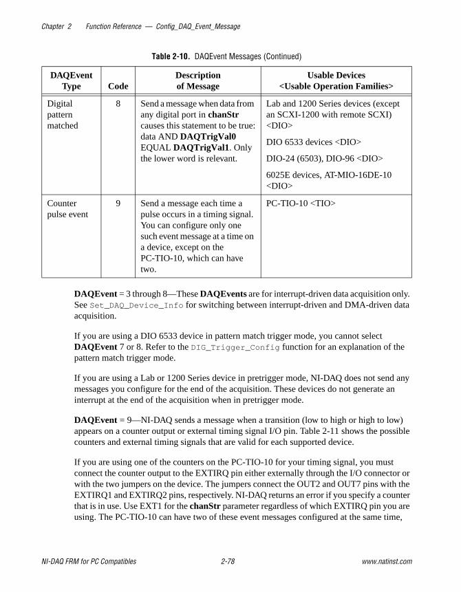
Chapter 2 Function Reference — Config_DAQ_Event_Message
NI-DAQ FRM for PC Compatibles 2-78 www.natinst.com
DAQEvent = 3 through 8—These DAQEvents are for interrupt-driven data acquisition only. See Set_DAQ_Device_Info for switching between interrupt-driven and DMA-driven data acquisition.
If you are using a DIO 6533 device in pattern match trigger mode, you cannot select DAQEvent 7 or 8. Refer to the DIG_Trigger_Config function for an explanation of the pattern match trigger mode.
If you are using a Lab or 1200 Series device in pretrigger mode, NI-DAQ does not send any messages you configure for the end of the acquisition. These devices do not generate an interrupt at the end of the acquisition when in pretrigger mode.
DAQEvent = 9—NI-DAQ sends a message when a transition (low to high or high to low) appears on a counter output or external timing signal I/O pin. Table 2-11 shows the possible counters and external timing signals that are valid for each supported device.
If you are using one of the counters on the PC-TIO-10 for your timing signal, you must connect the counter output to the EXTIRQ pin either externally through the I/O connector or with the two jumpers on the device. The jumpers connect the OUT2 and OUT7 pins with the EXTIRQ1 and EXTIRQ2 pins, respectively. NI-DAQ returns an error if you specify a counter that is in use. Use EXT1 for the chanStr parameter regardless of which EXTIRQ pin you are using. The PC-TIO-10 can have two of these event messages configured at the same time,
Digital pattern matched
8 Send a message when data from any digital port in chanStr causes this statement to be true:data AND DAQTrigVal0 EQUAL DAQTrigVal1 . Only the lower word is relevant.
Lab and 1200 Series devices (except an SCXI-1200 with remote SCXI) <DIO>
DIO 6533 devices <DIO>
DIO-24 (6503), DIO-96 <DIO>
6025E devices, AT-MIO-16DE-10 <DIO>
Counter pulse event
9 Send a message each time a pulse occurs in a timing signal. You can configure only one such event message at a time on a device, except on the PC-TIO-10, which can have two.
PC-TIO-10 <TIO>
Table 2-10. DAQEvent Messages (Continued)
DAQEvent Type Code
Descriptionof Message
Usable Devices<Usable Operation Families>

Chapter 2 Function Reference — Config_DAQ_Event_Message
© National Instruments Corporation 2-79 NI-DAQ FRM for PC Compatibles
therefore you must specify which pin you want to use on the PC-TIO-10 with the DAQTrigVal0 parameter.
To use DAQEvent = 9, you must configure the device for interrupt-driven waveform generation. This DAQEvent works by using the waveform generation timing system. Thus, you cannot use waveform generation or single point analog output with delayed update mode and this DAQEvent at the same time on the same device. Also, DAQEvent = 9 is not valid for the E Series devices.
trigSkipCount is the number of valid triggers NI-DAQ ignores. It can be any value greater than or equal to zero. For example, if trigSkipCount is 3, NI-DAQ notifies you when the fourth trigger occurs.
preTrigScans is the number of scans of data NI-DAQ collects before looking for the very first trigger. Setting preTrigScans to 0 causes NI-DAQ to look for the first trigger as soon as the DAQ process begins.
postTrigScans is the number of scans of data NI-DAQ collects after the triggers before notifying you. Setting postTrigScans to 0 causes event notification to happen as soon as the trigger occurs.
Refer to the following table for further details on usable parameters for each DAQEvent type.
Table 2-11. Valid Counters and External Timing Signals for DAQEvent = 9
Data Acquisition Device I/O Pin I/O Pin State Change
PC-TIO-10 EXTIRQ1 or EXTIRQ2 high to low

Chapter2Function Reference
—Config_DAQ_Event_M
essage
NI-DAQ FRM for PC Com
patibles2-80
ww
w.natinst.com
Table 2-12. Usable Parameters for Different DAQEvent Codes
Parameter
DAQEvent
0 1 2 3 4 5 6 7 8 9
chanStr (where n and m are numbers)
AIn, DIn, DOn, SCn!..., AMn!m,AOn
AIn, DIn, DOn, SCn!..., AMn!m, AOn
AIn, AOn, DIn, DOn, SCn!..., AMn!m
AIn, SCn!..., AMn!m
AIn, SCn!..., AMn!m
AIn, SCn!..., AMn!m
AIn, SCn!..., AMn!m
DIn, DOn DIn, DOn CTRn, EXT1
DAQTrigVal0 no. of scans, must be greater than 0
no. of scans, must be greater than 0 (see note below)
ignored upper bound for analog alarm region (binary), must be greater than or equal to DAQTrigVal1
upper bound for analog alarm region (binary), must be greater than or equal to DAQTrigVal1
upper bound for hysteresis window (binary), must be greater than or equal to DAQTrigVal1
upper bound for hysteresis window (binary), must be greater than or equal to DAQTrigVal1
digital pattern mask (decimal)
digital pattern mask (decimal)
EXTIRQ no. (1 or 2) if chanStr = EXTn for the PC-TIO-10, otherwise ignored
DAQTrigVal1 ignored ignored ignored lower bound for analog alarm region (binary)
lower bound for analog alarm region (binary)
lower bound for hysteresis window (binary)
lower bound for hysteresis window (binary)
digital pattern not to match (decimal)
digital pattern to match (decimal)
ignored
trigSkipCount ignored ignored ignored ignored ignored no. of triggers to skip
no. of triggers to skip
ignored ignored ignored
preTrigScans ignored ignored ignored ignored ignored no. of scans before trigger condition is met
no. of scans before trigger condition is met
ignored ignored ignored
postTrigScans ignored ignored ignored ignored ignored no. of scans after trigger condition is met
no. of scans after trigger condition is met
ignored ignored ignored

Chapter 2 Function Reference — Config_DAQ_Event_Message
© National Instruments Corporation 2-81 NI-DAQ FRM for PC Compatibles
For the parameters that are ignored, set them to 0.
For DAQEvent = 1, DAQTrigVal0 must be greater than zero. If you are using DMA with double buffers or a pretrigger data acquisition, DAQTrigVal0 must be an even divisor of the buffer size in scans.
For DAQEvent = 1 on an analog output channel, DAQTrigVal0 must always be an even divisor of the buffer size or a multiple of it.
handle is the handle to the window you want to receive a Windows message in when DAQEvent happens. If handle is 0, no Windows messages are sent.
message is a message you define. When DAQEvent happens, NI-DAQ passes message back to you. message can be any value.
callbackAddr is the address of the user callback function. NI-DAQ calls this function when DAQEvent occurs. If you do not want to use a callback function, set callbackAddr to 0.
Using This FunctionThis function notifies your application when DAQEvent occurs. Using DAQEvent eliminates continuous polling of asynchronous operations through NI-DAQ functions.
For example, if you have a double-buffered DAQ application, instead of calling DAQ_DB_HalfReady continuously, you can call Config_DAQ_Event_Message and set DAQEvent to 1 and DAQTrigVal0 to be one-half your buffer size in units of scans. Then, NI-DAQ notifies your application when it is time to call DAQ_DB_Transfer . The same concept applies to digital input/output block functions and analog output functions.
To define a message, call Config_DAQ_Event_Message before starting your DAQ process. You can associate more than one message to the same device by calling Config_DAQ_Event_Message as many times as you need to.
After you define a message, it remains active until you call Config_DAQ_Event_Message or Init_DA_Brds to remove messages. To remove a specific message, call Config_DAQ_Event_Message with mode set to 2. When removing a specific message, make sure to provide all the information defining the message, such as chanStr (SCXIchassisID, moduleSlot, chanType, chan), DAQEvent, DAQTrigVal0 , DAQTrigVal1 , trigSkipCount , preTrigScans, postTrigScans, handle, message, and callbackAddr.
To remove all messages associated with the device, call Config_DAQ_Event_Message with mode set to zero and with all other arguments except deviceNumber set to zero.

Chapter 2 Function Reference — Config_DAQ_Event_Message
NI-DAQ FRM for PC Compatibles 2-82 www.natinst.com
Event notification is done through the Windows API function PostMessage and/or a callback function that you define.
When any trigger event happens, NI-DAQ calls PostMessage as follows:
int PostMessage(HWND handle, UINT message, WPARAM wParam,
LPARAM lParam)
handle and message are the same handle and message as previously defined. The least significant byte of wParam is the device and the second least significant byte of wParam is a Boolean flag, doneFlag, indicating whether the DAQ process has ended.
doneFlag = 0: Asynchronous operation is still running.doneFlag = 1: Asynchronous operation has stopped.
lParam contains the number of the scan in which DAQEvent occurred.
The following is an example WindowProc routine, written in C:
LRESULT CALLBACK WindowProc(HWND hWnd, UINT uMsgId, WPARAM wParam, LPARAM
lParam)
static unsigned long int uNIDAQeventCount = 0;
short DAQeventDevice;
short doneFlag;
long scansDone;
switch (uMsgId)
case WM_PAINT:
//..handle this message...
break;
case WM_DESTROY:
//..handle this message...
break;
case WM_NIDAQ_MSG:
//**************************************
//put your NI-DAQ Message handling here!
//**************************************
// increment static counter
uNIDAQeventCount++;
DAQeventDevice = (wParam & 0x00FF);
doneFlag = (wParam & 0xFF00) >> 8;
scansDone = lParam;
//..handle this message...
return 0;
break;

Chapter 2 Function Reference — Config_DAQ_Event_Message
© National Instruments Corporation 2-83 NI-DAQ FRM for PC Compatibles
default:
// handle other usual messages...
return DefWindowProc (hWnd, uMsgId, wParam, lParam);
Callback FunctionsTo enable the callback function, you need to provide the address of the callback routine in callbackAddr. Therefore, you must write your application in a programming language that supports function pointers, such as C or Assembly.
If you are using LabWindows/CVI, your callback function is called by means of messaging. If you are using LabWindows/CVI 4.0.1, you must take special precautions to prevent multiple accesses to non-multithread-safe libraries from the DAQEvent callback function.
Callback Functions in Windows 98/95 and Windows NTCallbacks are easy and safe to use in Windows 98/95 and Windows NT. Your callback function is called in the foreground and in the context of your process. You can access your global data, make system calls, or call NI-DAQ from your callback function. However, succeeding events will not be handled until your callback has returned. The time delay between the event and notification (also known as latency) is highly variable and depends largely on how loaded your system is. Latency is always less with a callback than a Windows message because you avoid the latency of the Windows messaging system.
Latency is less deterministic with packet-based buses, such as the Universal Serial Bus (USB).
Your callback function should use standard C calling conventions. Do not use the CALLBACK function type. Here is a sample prototype:
void myCallback (HWND hwnd, UINT message, WPARAM wparam, LPARAM
lparam)

Chapter 2 Function Reference — Configure_HW_Analog_Trigger
NI-DAQ FRM for PC Compatibles 2-84 www.natinst.com
Configure_HW_Analog_Trigger
Formatstatus = Configure_HW_Analog_Trigger (deviceNumber, onOrOff, lowValue, highValue,
mode, trigSource)
PurposeConfigures the hardware analog trigger. The hardware analog triggering circuitry produces a digital trigger that you can use for any of the signals available through the Select_Signal function by selecting source = ND_PFI_0 .
ParametersInput
Parameter DiscussionLegal ranges for the onOrOff , mode, and trigSource parameters are given in terms of constants that are defined in a header file. The header file you should use depends on which of the following languages you are using:
• C programmers—NIDAQCNS.H (DATAACQ.H for LabWindows/CVI)
• BASIC programmers—NIDAQCNS.INC (Visual Basic for Windows programmers should refer to the Programming Language Considerations section in Chapter 1, Using the NI-DAQ Functions, for more information.)
• Pascal programmers—NIDAQCNS.PAS
onOrOff informs NI-DAQ whether you want to turn the analog trigger on or off. Legal values for this parameter are ND_ON and ND_OFF.
Name Type Description
deviceNumber i16 assigned by configuration utility
onOrOff u32 turns the analog trigger on or off
lowValue i32 specifies the low level used for analog triggering
highValue i32 specifies the high level used for analog triggering
mode u32 the way the triggers are generated
trigSource u32 the source of the signal used for triggering

Chapter 2 Function Reference — Configure_HW_Analog_Trigger
© National Instruments Corporation 2-85 NI-DAQ FRM for PC Compatibles
lowValue and highValue specify the levels you want to use for triggering. For E Series devices, the legal range for the two values is 0 to 255 (0–4,095 for 16-bit boards). In addition, lowValue must be less than highValue. The voltage levels corresponding to lowValue and highValue are as follows:
• When trigSource = ND_PFI_0 , 0 corresponds to –10 V and 255 (4,095 for the 16-bit boards) corresponds to +10 V; values between 0 and 255 (4,095 for 16-bit boards) are distributed evenly between –10 V and +10 V. You can use ND_PFI_0 as the analog signal you are triggering off of at the same time you designate ND_PFI_0 as a source for a Select_Signal signal.
• When trigSource = ND_THE_AI_CHANNEL and the channel is in bipolar mode, the following conditions apply:
– Most Boards—0 corresponds to –5 V, 255 corresponds to +5 V; values between 0 and 255 are evenly distributed between –5 V and +5 V.
– 61XX Devices—0 corresponds to –10 V; 255 corresponds to +10 V; and values between 0 and 255 are evenly distributed between –10 V and +10 V.
– 16-Bit Boards—0 corresponds to –10 V; 4,095 corresponds to +10 V; and values between 0 and 4,095 are evenly distributed between –10 V and +10 V.
• When trigSource = ND_THE_AI_CHANNEL and the channel is in unipolar mode, the following conditions apply:
– 12-Bit Boards—0 corresponds to 0 V; 255 corresponds to +10 V; and values between 0 and 255 are evenly distributed between 0 V and +10 V.
– Most 16-Bit Boards—2,048 corresponds to 0 V; 4,095 corresponds to +10 V; and values between 2,048 and 4,095 are evenly distributed between 0 V and +10 V.
– 6052E Boards—0 corresponds to 0 V; 4,095 corresponds to +10 V; and values between 0 and 4,095 are evenly distributed between 0 V and +10 V.
See the end of this section for an example calculation for lowValue.
For DSA devices, the legal range for lowValue and highValue is –32,768 to +32,767. These values correspond to the lower limit of the voltage range to the higher limit of the voltage range for the current configuration of the trigger channel. For example, when the channel is configured for 0 dB of gain, –32,768 corresponds to –10 V and +32,767 corresponds to +10 V.
mode tells NI-DAQ how you want analog triggers to be converted into digital triggers that the onboard hardware can use for timing.
Note The PCI-6110E and PCI-6111E can use any of the analog input channels for the trigSource. For these devices set trigSource to the channel number you want, instead of the constant ND_THE_AI_CHANNEL.

Chapter 2 Function Reference — Configure_HW_Analog_Trigger
NI-DAQ FRM for PC Compatibles 2-86 www.natinst.com
Note This also applies to the 445X and 455X devices.
The following paragraphs and figures show all of the available modes and illustrations of corresponding trigger generation scenarios. Values specified by highValue and lowValue are represented using dashed lines, and the signal used for triggering is represented using a solid line.
• ND_BELOW_LOW_LEVEL—The trigger is generated when the signal value is less than the lowValue. highValue is unused.
Figure 2-4. ND_BELOW_LOW_LEVEL
• ND_ABOVE_HIGH_LEVEL—The trigger is generated when the signal value is greater than the highValue. lowValue is unused.
Figure 2-5. ND_ABOVE_HIGH_LEVEL
• ND_INSIDE_REGION—The trigger is generated when the signal value is between the lowValue and the highValue.
lowValue
Trigger
highValue
Trigger

Chapter 2 Function Reference — Configure_HW_Analog_Trigger
© National Instruments Corporation 2-87 NI-DAQ FRM for PC Compatibles
Figure 2-6. ND_INSIDE_REGION
• ND_HIGH_HYSTERESIS—The trigger is generated when the signal value is greater than the highValue, with hysteresis specified by lowValue.
Figure 2-7. ND_HIGH_HYSTERESIS
• ND_LOW_HYSTERESIS—The trigger is generated when the signal value is less than the lowValue, with hysteresis specified by highValue.
Figure 2-8. ND_LOW_HYSTERESIS
Use the trigSource parameter to specify the source of the trigger you want to use. For E Series devices, the legal values are ND_PFI_0 and ND_THE_AI_CHANNEL.
highValue
Trigger
lowValue
highValue
Trigger
lowValue
highValue
Trigger
lowValue

Chapter 2 Function Reference — Configure_HW_Analog_Trigger
NI-DAQ FRM for PC Compatibles 2-88 www.natinst.com
Set trigSource to ND_PFI_0 if you want the trigger to come from the PFI0/TRIG1 pin. You need to connect the analog signal you want to use for triggering to the PFI0/TRIG1 pin. To generate triggers based on an analog signal that takes a wide range of values between –10 V and +10 V, you should use this setting.
You should select ND_THE_AI_CHANNEL for trigSource only to generate triggers based on a low-range analog signal, if you are concerned about signal quality and are using a shielded cable, or if you want the trigger to be based on an analog input channel in the differential mode. Using this selection is non-trivial.
If you set trigSource to ND_THE_AI_CHANNEL, you can use the signal connected to one of the analog input pins for triggering. In this case, the signal is amplified on the device before it is used for trigger generation. You can use this source selection under the following conditions:
• You want to perform data acquisition from a single analog input channel (the DAQ family of functions). You can use only the channel you are acquiring data from for analog triggering.
• You want to perform data acquisition from more than one analog input channel (a combination of the DAQ and SCAN families of functions). The only analog input channel you can use as the start trigger is the first channel from your list of channels. You cannot use this form of the analog trigger for the stop trigger in case of pretriggered data acquisition.
Note The PCI-6110E and PCI-6111E can use any analog input channel.
• You do not want to perform any analog input operations (the AI , DAQ, and SCAN families of functions). You must use AI_Setup to select the analog input channel you want to use and the gain of the instrumentation amplifier. You also can use AI_Configure to alter the configuration of the analog input channel.
• You want to use AI_Check , and you want to use the analog trigger for conversion timing. You do not have to perform any special steps.
The reason for using these constraints is that if you are scanning among several analog input channels, signals from those channels are multiplexed in time, and the analog triggering circuitry is unable to distinguish between signals from individual channels in this case.
For DSA devices only, any of the analog input channels can be the source of the analog trigger, even channels that are not part of the channel list set in DAQ_Start or SCAN_Setup . Set trigSource to the channel number of the channel to monitor for the analog trigger.

Chapter 2 Function Reference — Configure_HW_Analog_Trigger
© National Instruments Corporation 2-89 NI-DAQ FRM for PC Compatibles
Using This FunctionWhen you use this function, you activate the onboard analog triggering hardware. This onboard hardware generates a digital trigger that the DAQ-STC then uses for timing and control. To use the analog trigger, you need to use this function and the Select_Signal function. To use analog triggering, use as much hysteresis as your application allows because the circuitry used for this purpose is very noise-sensitive.
For E series devices, when you use Select_Signal , set source to ND_PFI_0 for your signal, and set sourceSpec as appropriate. Notice that the two polarity selections give you timing control in addition to the five triggering modes listed here. For DSA devices, when you use Select_Signal , set source to ND_ATC_OUT for your signal, and set sourceSpec to ND_DONT_CARE. NI-DAQ will route the analog trigger circuit output as appropriate for the device.
For example, if you set source to ND_THE_AI_CHANNEL, the channel you are interested in is in bipolar mode, you want a gain of 100, and you want to set the voltage window for triggering to +35 mV and +45 mV for your original signal (that is, signal before amplification by the onboard amplifier), you should make the following programming sequence:
12-bit boards:
status = Configure_HW_Analog_Trigger (deviceNumber, ND_ON, 218, 243, mode, ND_THE_AI_CHANNEL)
Status = Select_Signal (deviceNumber, ND_IN_START_TRIGGER, ND_PFI_0 , ND_LOW_TO_HIGH)
16-bit boards:
status = Configure_HW_Analog_Trigger (deviceNumber, ND_ON, 2764, 2969, mode, ND_THE_AI_CHANNEL)
status = Select_Signal (deviceNumber, ND_IN_START_TRIGGER, ND_PFI_0 , ND_LOW_TO_HIGH)
To calculate lowValue in the previous example, do the following:
1. Multiply 35 mV by 100 to adjust for the gain to get 3.5 V.
2. Use the following formula to map the 3.5 V from the –5 V to +5 V scale to a value on the 0 to 255 (0–4,095 for the 16-bit boards) scale:
value = (3.5/5 + 1) * 128 = 218 (for the 0 to 255 case)
Use the following formula to map the 3.5 V from the –10 V to +10 V scale to a value on the 0 to 4,095 scale:
value = (3.5/10 + 1) * 2,048 = 2,764 (for the 0 to 4,095 case)
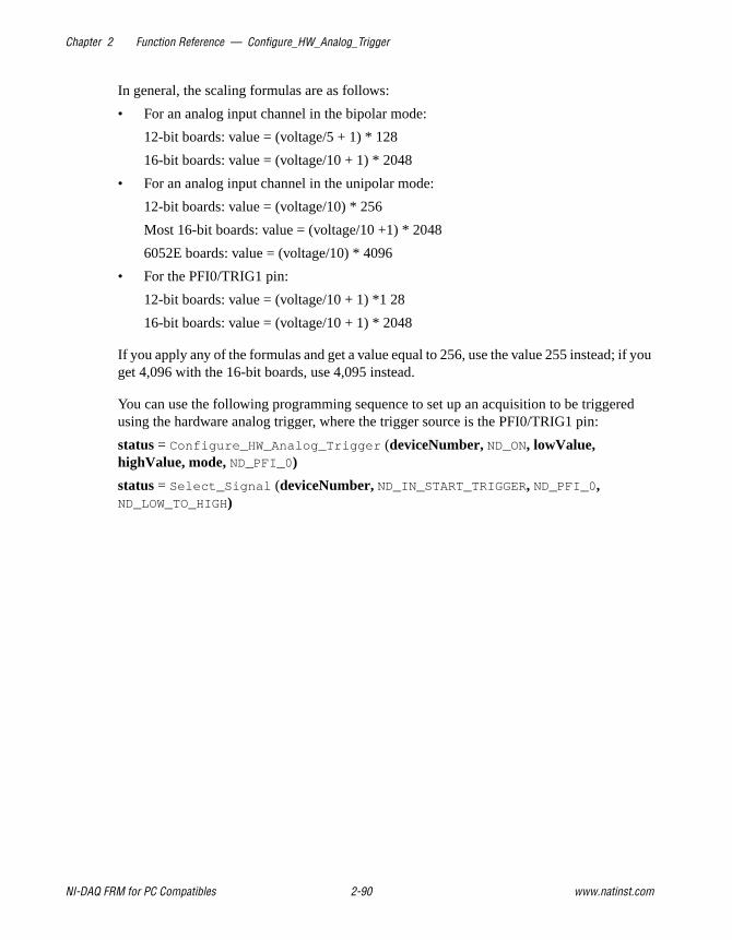
Chapter 2 Function Reference — Configure_HW_Analog_Trigger
NI-DAQ FRM for PC Compatibles 2-90 www.natinst.com
In general, the scaling formulas are as follows:
• For an analog input channel in the bipolar mode:
12-bit boards: value = (voltage/5 + 1) * 128
16-bit boards: value = (voltage/10 + 1) * 2048
• For an analog input channel in the unipolar mode:
12-bit boards: value = (voltage/10) * 256
Most 16-bit boards: value = (voltage/10 +1) * 2048
6052E boards: value = (voltage/10) * 4096
• For the PFI0/TRIG1 pin:
12-bit boards: value = (voltage/10 + 1) *1 28
16-bit boards: value = (voltage/10 + 1) * 2048
If you apply any of the formulas and get a value equal to 256, use the value 255 instead; if you get 4,096 with the 16-bit boards, use 4,095 instead.
You can use the following programming sequence to set up an acquisition to be triggered using the hardware analog trigger, where the trigger source is the PFI0/TRIG1 pin:
status = Configure_HW_Analog_Trigger (deviceNumber, ND_ON, lowValue, highValue, mode, ND_PFI_0 )
status = Select_Signal (deviceNumber, ND_IN_START_TRIGGER, ND_PFI_0 , ND_LOW_TO_HIGH)

Chapter 2 Function Reference — CTR_Config
© National Instruments Corporation 2-91 NI-DAQ FRM for PC Compatibles
CTR_Config
Formatstatus = CTR_Config (deviceNumber, ctr, edgeMode, gateMode, outType, outPolarity)
PurposeSpecifies the counting configuration to use for a counter.
ParametersInput
Parameter Discussionctr is the counter number.Range: 1 through 10 for a PC-TIO-10.
edgeMode indicates which edge of the input signal that the counter should count. edgeMode must be either 0 or 1.
0: counter counts rising edges.1: counter counts falling edges.
gateMode selects the gating mode to be used by the counter. There are eight different gating modes. Each gating mode has been assigned a number between 0 and 7. The available gating modes are as follows:
0: No gating used.1: High-level gating of counter ctr used.2: Low-level gating of counter ctr used.3: Edge-triggered gating used—rising edge of counter ctr .4: Edge-triggered gating used—falling edge of counter ctr .5: Active high on terminal count of next lower-order counter.6: Active high on gate of next higher-order counter.
Name Type Description
deviceNumber i16 assigned by configuration utility
ctr i16 counter number
edgeMode i16 count rising or falling edges
gateMode i16 gating mode to be used
outType i16 type of output generated
outPolarity i16 output polarity

Chapter 2 Function Reference — CTR_Config
NI-DAQ FRM for PC Compatibles 2-92 www.natinst.com
7: Active high on gate of next lower-order counter.8: Special gating.
outType selects which type of output is to be generated by the counter. The counters generate two types of output signals: TC toggled output and TC pulse output.
0: TC toggled output type used.1: TC pulse output type used.
outPolarity selects the output polarity used by the counter.0: Positive logic output.1: Negative logic (inverted) output.
Using This FunctionIf you select TC pulse output type, outPolarity = 0 means that NI-DAQ generates active logic-high terminal count pulses. outPolarity = 1 means that NI-DAQ generates active logic-low terminal count pulses.
Similarly, if you select TC toggled output type, then outPolarity = 0 means the OUT signal toggles from low to high on the first TC. outPolarity = 1 means the OUT signal toggles from high to low on the first TC.
CTR_Config saves the parameters in the configuration table for the specified counter. NI-DAQ uses this configuration table when the counter is set up for an event-counting, pulse output, or frequency output operation. You can use CTR_Config to take advantage of the many counter modes.
The default settings for the counter configuration modes are as follows:
edgeMode = 0: Counter counts rising edges.gateMode = 0: No gating used.outType = 0: TC toggled output type used.outPolarity = 0: Positive logic output used.
To change the counter configuration from this default setting, you must call CTR_Config and indicate which configuration you want before initiating any other counter operation.
Counter configuration settings applied through this function persist when waveform generation functions use the same counter. For example, to externally trigger a waveform generation option, use this function to change the gatemode to 1 (high-level gating), and then call the waveform generation functions. The waveform generation is delayed until a high-level signal appears on the gate pin on the I/O connector. Notice that this is really not a trigger signal but is a gating signal because the waveform generation pauses if the gate goes low at any time. Because the Am9513 counter/timer chip has certain limitations, you cannot use gateModes 3 and 4. You are responsible for producing a signal that stays high for the duration of the waveform generation operation.

Chapter 2 Function Reference — CTR_EvCount
© National Instruments Corporation 2-93 NI-DAQ FRM for PC Compatibles
CTR_EvCount
Formatstatus = CTR_EvCount (deviceNumber, ctr, timebase, cont)
PurposeConfigures the specified counter for an event-counting operation and starts the counter.
ParametersInput
Parameter Discussionctr is the counter number.Range: 1 through 10 for a PC-TIO-10.timebase selects the timebase, or resolution, to be used by the counter. timebase has the
following possible values:–1: Internal 5 MHz clock used as timebase (200 ns resolution).0: TC signal of ctr -1 used as timebase.1: Internal 1 MHz clock used as timebase (1 µs resolution).2: Internal 100 kHz clock used as timebase (10 µs resolution).3: Internal 10 kHz clock used as timebase (100 µs resolution).4: Internal 1 kHz clock used as timebase (1 ms resolution).5: Internal 100 Hz clock used as timebase (10 ms resolution).6: SOURCE1 used as timebase if 1 ≤ ctr ≤ 5 or SOURCE 6 used as timebase
if 6 ≤ ctr ≤ 10.7: SOURCE2 used as timebase if 1 ≤ ctr ≤ 5 or SOURCE 7 used as timebase
if 6 ≤ ctr ≤ 10.8: SOURCE3 used as timebase if 1 ≤ ctr ≤ 5 or SOURCE 8 used as timebase
if 6 ≤ ctr ≤ 10.9: SOURCE4 used as timebase if 1 ≤ ctr ≤ 5 or SOURCE 9 used as timebase
if 6 ≤ ctr ≤ 10.10: SOURCE5 used as timebase if 1 ≤ ctr ≤ 5 or SOURCE 10 used as timebase
if 6 ≤ ctr ≤ 10.
Name Type Description
deviceNumber i16 assigned by configuration utility
ctr i16 counter number
timebase i16 timebase value
cont i16 whether counting continues

Chapter 2 Function Reference — CTR_EvCount
NI-DAQ FRM for PC Compatibles 2-94 www.natinst.com
11: GATE 1 used as timebase if 1 ≤ ctr ≤ 5 or GATE6 used as timebase if 6 ≤ ctr ≤ 10.
12: GATE 2 used as timebase if 1 ≤ ctr ≤ 5 or GATE7 used as timebase if 6 ≤ ctr ≤ 10.
13: GATE 3 used as timebase if 1 ≤ ctr ≤ 5 or GATE8 used as timebase if 6 ≤ ctr ≤ 10.
14: GATE 4 used as timebase if 1 ≤ ctr ≤ 5 or GATE9 used as timebase if 6 ≤ ctr ≤ 10.
15: GATE 5 used as timebase if 1 ≤ ctr ≤ 5 or GATE10 used as timebase if 6 ≤ ctr ≤ 10.
Set timebase to zero to concatenate counters. Set timebase to 1 through 5 for the counter to count one of the five available internal signals. Set timebase to 6 through 15 (except 10 for the PC-TIO-10) to provide an external signal to a counter. This external signal is then the signal NI-DAQ counts for event counting.
cont indicates whether counting continues after the counter reaches 65,535 and rolls over to zero. cont can be either 0 or 1. If cont = 0, event counting stops when the counter reaches 65,535 and rolls over, in which case an overflow condition is registered. If cont = 1, event counting continues when the counter rolls over and no overflow condition is registered. cont = 1 is useful when more than one counter is concatenated for event counting.
Using This FunctionCTR_EvCount configures the specified counter for an event-counting operation. The function configures the counter to count up from zero and to use the gating mode, edge mode, output type, and polarity as specified by the CTR_Config call.
Note Edge gating mode does not operate properly during event counting if cont = 1. If cont = 1, use level gating modes or no-gating mode.
Applications for CTR_EvCount are discussed in Event-Counting Applications in Chapter 3, Software Overview, of the NI-DAQ User Manual for PC Compatibles.

Chapter 2 Function Reference — CTR_EvRead
© National Instruments Corporation 2-95 NI-DAQ FRM for PC Compatibles
CTR_EvRead
Formatstatus = CTR_EvRead (deviceNumber, ctr, overflow, count)
PurposeReads the current counter total without disturbing the counting process and returns the count and overflow conditions.
ParametersInput
Output
Parameter Discussionctr is the counter number.Range: 1 through 10 for a PC-TIO-10.
overflow returns the overflow state of the counter. A counter overflows if it counts up to 65,535 and rolls over to zero on the next count. If overflow = 0, no overflow has occurred. If overflow = 1, an overflow occurred. See the Special Considerations for Overflow Detection section later in this function description.
count returns the current total of the specified counter. count can be between zero and 65,535. count represents the number of edges (either falling or rising edges, not both) that have occurred since the counter started counting.
Note C Programmers—overflow and count are pass-by-address parameters.
Name Type Description
deviceNumber i16 assigned by configuration utility
ctr i16 counter number
Name Type Description
overflow *i16 overflow state of the counter
count *u16 current total of the specified counter

Chapter 2 Function Reference — CTR_EvRead
NI-DAQ FRM for PC Compatibles 2-96 www.natinst.com
Using This FunctionCTR_EvRead reads the current value of the counter without disturbing the counting process and returns the value in count. CTR_EvRead also performs overflow detection and returns the overflow status in overflow. Overflow detection and the significance of count depend on the counter configuration.
Special Considerations for Overflow DetectionFor NI-DAQ to detect an overflow condition, you must configure the counter for TC toggled output type and positive output polarity, and then you must configure the counter to stop counting on overflow (cont = 0 in the CTR_EvCount call). If these conditions are not met, the value of overflow is meaningless. If more than one counter is concatenated for event-counting applications, you should configure the lower-order counters to continue counting when overflow occurs, and overflow detection is only meaningful for the highest order counter. count, returned by CTR_EvRead for the lower-order counters, then represents the module 65,536 event count. See Event-Counting Applications in Chapter 3, Software Overview, in the NI-DAQ User Manual for PC Compatibles for more information.

Chapter 2 Function Reference — CTR_FOUT_Config
© National Instruments Corporation 2-97 NI-DAQ FRM for PC Compatibles
CTR_FOUT_Config
Formatstatus = CTR_FOUT_Config (deviceNumber, FOUT_port, mode, timebase, division)
PurposeDisables or enables and sets the frequency of the 4-bit programmable frequency output.
ParametersInput
Parameter DiscussionFOUT_port is the frequency output port to be programmed.
1: For FOUT1 on the PC-TIO-10.2: For FOUT2 on the PC-TIO-10.
mode selects whether to enable or disable the programmable frequency output. mode can be 0 or 1.
0: The frequency output signal is turned off to a low-logic state.1: The frequency output signal is enabled.
If mode = 0, none of the following parameters apply.
timebase selects the timebase, or resolution, to be used by the programmable frequency output. timebase has the following possible values:
–1: Internal 5 MHz clock used as timebase (200 ns resolution).1: Internal 1 MHz clock used as timebase (1 µs resolution).2: Internal 100 kHz clock used as timebase (10 µs resolution).3: Internal 10 kHz clock used as timebase (100 µs resolution).4: Internal 1 kHz clock used as timebase (1 ms resolution).5: Internal 100 Hz clock used as timebase (10 ms resolution).
Name Type Description
deviceNumber i16 assigned by configuration utility
FOUT_port i16 frequency output port
mode i16 enable or disable the programmable frequency output
timebase i16 timebase value
division i16 divide-down factor for generating the clock

Chapter 2 Function Reference — CTR_FOUT_Config
NI-DAQ FRM for PC Compatibles 2-98 www.natinst.com
6: SOURCE1 used as timebase if FOUT_port = 1 or SOURCE 6 used as timebase if FOUT_port = 2.
7: SOURCE2 used as timebase if FOUT_port = 1 or SOURCE 7 used as timebase if FOUT_port = 2.
8: SOURCE3 used as timebase if FOUT_port = 1 or SOURCE 8 used as timebase if FOUT_port = 2.
9: SOURCE4 used as timebase if FOUT_port = 1 or SOURCE 9 used as timebase if FOUT_port = 2.
10: SOURCE5 used as timebase if FOUT_port = 1 or SOURCE 10 used as timebase if FOUT_port = 2.
11: GATE 1 used as timebase if FOUT_port = 1 or GATE6 used as timebase if FOUT_port = 2.
12: GATE 2 used as timebase if FOUT_port = 1 or GATE7 used as timebase if FOUT_port = 2.
13: GATE 3 used as timebase if FOUT_port = 1 or GATE8 used as timebase if FOUT_port = 2.
14: GATE 4 used as timebase if FOUT_port = 1 or GATE9 used as timebase if FOUT_port = 2.
15: GATE 5 used as timebase if FOUT_port = 1 or GATE10 used as timebase if FOUT_port = 2.
division is the divide-down factor for generating the clock. The clock frequency is then equal to (timebase frequency)/division.Range: 1 through 16.
Using This FunctionCTR_FOUT_Config generates a 50% duty-cycle output clock at the programmable frequency output signal FOUT if mode = 1; otherwise, the FOUT signal is a low-logic state. The frequency of the FOUT signal is the frequency corresponding to timebase divided by the division factor.

Chapter 2 Function Reference — CTR_Period
© National Instruments Corporation 2-99 NI-DAQ FRM for PC Compatibles
CTR_Period
Formatstatus = CTR_Period (deviceNumber, ctr, timebase)
PurposeConfigures the specified counter for period or pulse-width measurement.
ParametersInput
Parameter Discussionctr is the counter number.Range: 1 through 10 for a PC-TIO-10.
timebase selects the timebase, or resolution, to be used by the counter. timebase has the following possible values:
–1: Internal 5 MHz clock used as timebase (200 ns resolution).0: TC signal of ctr -1 used as timebase.1: Internal 1 MHz clock used as timebase (1 µs resolution).2: Internal 100 kHz clock used as timebase (10 µs resolution).3: Internal 10 kHz clock used as timebase (100 µs resolution).4: Internal 1 kHz clock used as timebase (1 ms resolution).5: Internal 100 Hz clock used as timebase (10 ms resolution).6: SOURCE1 used as timebase if 1 ≤ ctr ≤ 5 or SOURCE 6 used as timebase
if 6 ≤ ctr ≤ 10.7: SOURCE2 used as timebase if 1 ≤ ctr ≤ 5 or SOURCE 7 used as timebase
if 6 ≤ ctr ≤ 10.8: SOURCE3 used as timebase if 1 ≤ ctr ≤ 5 or SOURCE 8 used as timebase
if 6 ≤ ctr ≤ 10.9: SOURCE4 used as timebase if 1 ≤ ctr ≤ 5 or SOURCE 9 used as timebase
if 6 ≤ ctr ≤ 10.10: SOURCE5 used as timebase if 1 ≤ ctr ≤ 5 or SOURCE 10 used as timebase
if 6 ≤ ctr ≤ 10.
Name Type Description
deviceNumber i16 assigned by configuration utility
ctr i16 counter number
timebase i16 timebase value

Chapter 2 Function Reference — CTR_Period
NI-DAQ FRM for PC Compatibles 2-100 www.natinst.com
11: GATE 1 used as timebase if 1 ≤ ctr ≤ 5 or GATE6 used as timebase if 6 ≤ ctr ≤ 10.
12: GATE 2 used as timebase if 1 ≤ ctr ≤ 5 or GATE7 used as timebase if 6 ≤ ctr ≤ 10.
13: GATE 3 used as timebase if 1 ≤ ctr ≤ 5 or GATE8 used as timebase if 6 ≤ ctr ≤ 10.
14: GATE 4 used as timebase if 1 ≤ ctr ≤ 5 or GATE9 used as timebase if 6 ≤ ctr ≤ 10.
15: GATE 5 used as timebase if 1 ≤ ctr ≤ 5 or GATE10 used as timebase if 6 ≤ ctr ≤ 10.
Set timebase to 0 to concatenate counters. Set timebase to 1 through 5 for the counter to count one of the five available internal signals. Set timebase to 6 through 15 (except 10 for the PC-TIO-10) to provide an external signal to a counter. This external signal becomes the signal NI-DAQ counts for event counting.
Using This FunctionCTR_Period configures the specified counter for period and pulse-width measurement. The function configures the counter to count up from zero and to use the gating mode, edge mode, output type, and polarity as specified by the CTR_Config call.
Applications for CTR_Period are discussed in the section Period and Continuous Pulse-Width Measurement Applications in Chapter 3, Software Overview, of the NI-DAQ User Manual for PC Compatibles.

Chapter 2 Function Reference — CTR_Pulse
© National Instruments Corporation 2-101 NI-DAQ FRM for PC Compatibles
CTR_Pulse
Formatstatus = CTR_Pulse (deviceNumber, ctr, timebase, delay, pulseWidth)
PurposeCauses the specified counter to generate a specified pulse-programmable delay and pulse width.
ParametersInput
Parameter Discussionctr is the counter number.Range: 1 through 10 for a PC-TIO-10.
timebase selects the timebase, or resolution, to be used by the counter. timebase has the following possible values:
–1: Internal 5 MHz clock used as timebase (200 ns resolution).0: TC signal of ctr–1 used as timebase.1: Internal 1 MHz clock used as timebase (1 µs resolution).2: Internal 100 kHz clock used as timebase (10 µs resolution).3: Internal 10 kHz clock used as timebase (100 µs resolution).4: Internal 1 kHz clock used as timebase (1 ms resolution).5: Internal 100 Hz clock used as timebase (10 ms resolution).6: SOURCE1 used as timebase if 1 ≤ ctr ≤ 5 or SOURCE 6 used as timebase
if 6 ≤ ctr ≤ 10.7: SOURCE2 used as timebase if 1 ≤ ctr v 5 or SOURCE 7 used as timebase
if 6 ≤ ctr ≤ 10.8: SOURCE3 used as timebase if 1 ≤ ctr ≤ 5 or SOURCE 8 used as timebase
if 6 ≤ ctr ≤ 10.
Name Type Description
deviceNumber i16 assigned by configuration utility
ctr i16 counter number
timebase i16 timebase value
delay u16 interval before the pulse
pulseWidth u16 interval of the pulse

Chapter 2 Function Reference — CTR_Pulse
NI-DAQ FRM for PC Compatibles 2-102 www.natinst.com
9: SOURCE4 used as timebase if 1 ≤ ctr ≤ 5 or SOURCE 9 used as timebase if 6 ≤ ctr ≤ 10.
10: SOURCE5 used as timebase if 1 ≤ ctr ≤ 5 or SOURCE 10 used as timebase if 6 ≤ ctr ≤ 10.
11: GATE 1 used as timebase if 1 ≤ ctr ≤ 5 or GATE6 used as timebase if 6 ≤ ctr ≤ 10.
12: GATE 2 used as timebase if 1 ≤ ctr ≤ 5 or GATE7 used as timebase if 6 ≤ ctr ≤ 10.
13: GATE 3 used as timebase if 1 ≤ ctr ≤ 5 or GATE8 used as timebase if 6 ≤ ctr ≤ 10.
14: GATE 4 used as timebase if 1 ≤ ctr ≤ 5 or GATE9 used as timebase if 6 ≤ ctr ≤ 10.
15: GATE 5 used as timebase if 1 ≤ ctr ≤ 5 or GATE10 used as timebase if 6 ≤ ctr ≤ 10.
Set timebase to 0 to concatenate counters. Set timebase to 1 through 5 for the counter to use one of the five available internal signals. Set timebase to 6 through 15 (except 10 for the PC-TIO-10) to provide an external clock to the counter.
delay is the delay before NI-DAQ generates the pulse. delay can be between 3 and 65,535. Use the following formula to determine the actual time period that delay represents:
delay * (timebase resolution)
pulseWidth is the width of the pulse NI-DAQ generates. pulseWidth can be between 0 and 65,535. Use the following formula to determine the actual time that pulseWidth represents:
pulseWidth * (timebase resolution)
for 1 ≤ pulseWidth ≤ 65,535. pulseWidth = 0 is a special case of pulse generation and actually generates a pulse of infinite duration (see the timing diagrams in Figures 2-9 and 2-10).
Using This FunctionCTR_Pulse sets up the counter to generate a pulse of the duration specified by pulseWidth, after a time delay of the duration specified by delay. If you specify no gating, CTR_Pulse starts the counter; otherwise, counter operation is controlled by the gate input. The selected timebase determines the timing of pulse generation as shown in Figure 2-9.
You can generate successive pulses by calling CTR_Restart or CTR_Pulse again. Be sure that the delay period of the previous pulse has elapsed before calling CTR_Restart or CTR_Pulse . A successive call waits until the previous pulse is completed before generating the next pulse. In the case where pulseWidth = 0 and TC toggle output is used, the output polarity toggles after every call to CTR_Restart .

Chapter 2 Function Reference — CTR_Pulse
© National Instruments Corporation 2-103 NI-DAQ FRM for PC Compatibles
Pulse Generation Timing ConsiderationsFigure 2-9 shows pulse generation timing for both the TC toggled output and TC pulse output cases. These signals are positive polarity output signals.
Figure 2-9. Pulse Generation Timing
An uncertainty is associated with the delay period due to counter synchronization. Counting starts on the first timebase edge after NI-DAQ applies the starting signal. The time between receipt of the starting pulse and start of pulse generation can be between (delay) and (delay + 1) units of the timebase in duration.
0 < sync period < 1
1
Timebase
Starting Signal
TC Toggle Output
TC Pulse Output 1
units = timebase period
- 1
1
1 1
delay pulse_width
delay - 1 pulse_width - 1

Chapter 2 Function Reference — CTR_Pulse
NI-DAQ FRM for PC Compatibles 2-104 www.natinst.com
pulseWidth = 0 generates a special case signal as shown in Figure 2-10.
Figure 2-10. Pulse Timing for pulseWidth = 0
0 < sync period < 1
1
Timebase
Starting Signal
TC ToggleOutput
TC Pulse Output 1
units = timebase period
delay
delay - 1
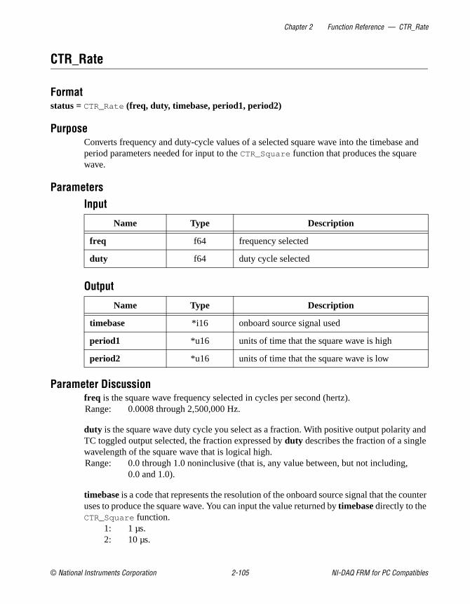
Chapter 2 Function Reference — CTR_Rate
© National Instruments Corporation 2-105 NI-DAQ FRM for PC Compatibles
CTR_Rate
Formatstatus = CTR_Rate (freq, duty, timebase, period1, period2)
PurposeConverts frequency and duty-cycle values of a selected square wave into the timebase and period parameters needed for input to the CTR_Square function that produces the square wave.
ParametersInput
Output
Parameter Discussionfreq is the square wave frequency selected in cycles per second (hertz).Range: 0.0008 through 2,500,000 Hz.
duty is the square wave duty cycle you select as a fraction. With positive output polarity and TC toggled output selected, the fraction expressed by duty describes the fraction of a single wavelength of the square wave that is logical high.Range: 0.0 through 1.0 noninclusive (that is, any value between, but not including,
0.0 and 1.0).
timebase is a code that represents the resolution of the onboard source signal that the counter uses to produce the square wave. You can input the value returned by timebase directly to the CTR_Square function.
1: 1 µs.2: 10 µs.
Name Type Description
freq f64 frequency selected
duty f64 duty cycle selected
Name Type Description
timebase *i16 onboard source signal used
period1 *u16 units of time that the square wave is high
period2 *u16 units of time that the square wave is low

Chapter 2 Function Reference — CTR_Rate
NI-DAQ FRM for PC Compatibles 2-106 www.natinst.com
3: 100 µs.4: 1 ms.5: 10 ms.
period1 and period2 represent the number of units of time (selected by timebase) that the square wave is high and low, respectively. The roles of period1 and period2 are reversed if the output polarity is negative.Range: 1 through 65,535.
Note C Programmers—timebase, period1, and period2 are pass-by-address parameters.
Using This FunctionCTR_Rate translates a definition of a square wave in terms of frequency and duty cycle into terms of a timebase and two period values. You can then input the timebase and period values directly into the CTR_Square function to produce the selected square wave.
CTR_Rate emphasizes matching the frequency first and then the duty cycle. That is, if the duty fraction is 0.5, but an odd-numbered total period is needed to produce the selected frequency, the two periods returned by CTR_Rate will not be equal and the duty cycle of the square wave differs slightly from 50 percent. For example, if freq is 40,000 Hz and duty is 0.50, CTR_Rate returns values of 1 for timebase, 13 for period1, and 12 for period2. The resulting square wave has the frequency of 40,000 Hz but a duty fraction of 0.52.

Chapter 2 Function Reference — CTR_Reset
© National Instruments Corporation 2-107 NI-DAQ FRM for PC Compatibles
CTR_Reset
Formatstatus = CTR_Reset (deviceNumber, ctr, output)
PurposeTurns off the specified counter operation and places the counter output drivers in the selected output state.
ParametersInput
Parameter Discussionctr is the counter number.Range: 1 through 10 for a PC-TIO-10.
output indicates the output state of the counter OUT signal driver. output can be between 0 and 2 and represents three choices of output state.
0: Set OUT signal driver to high-impedance state.1: Set OUT signal driver to low-logic state.2: Set OUT signal driver to high-logic state.
Using This FunctionCTR_Reset causes the specified counter to terminate its current operation, clears the counter mode, and places the counter OUT driver in the specified output state. When a counter has performed an operation (a square wave, for example), you must use CTR_Reset to stop and clear the counter before setting it up for any subsequent operation of a different type (event counting, for example). You also can use CTR_Reset to change the output state of an idle counter.
Name Type Description
deviceNumber i16 assigned by configuration utility
ctr i16 counter number
output i16 output state of the counter OUT signal driver

Chapter 2 Function Reference — CTR_Restart
NI-DAQ FRM for PC Compatibles 2-108 www.natinst.com
CTR_Restart
Formatstatus = CTR_Restart (deviceNumber, ctr)
PurposeRestarts operation of the specified counter.
ParametersInput
Parameter Discussionctr is the counter number.Range: 1 through 10 for a PC-TIO-10.
Using This FunctionYou can use CTR_Restart after a CTR_Stop operation to allow the suspended counter to resume. If the specified counter was never set up for an operation, CTR_Restart returns an error.
You also can use CTR_Restart after a CTR_Pulse operation to generate additional pulses. CTR_Pulse generates the first pulse. In this case, do not call CTR_Restart until after the previous pulse has completed.
Name Type Description
deviceNumber i16 assigned by configuration utility
ctr i16 counter number

Chapter 2 Function Reference — CTR_Simul_Op
© National Instruments Corporation 2-109 NI-DAQ FRM for PC Compatibles
CTR_Simul_Op
Formatstatus = CTR_Simul_Op (deviceNumber, numCtrs, ctrList, mode)
PurposeConfigures and simultaneously starts and stops multiple counters.
ParametersInput
Parameter DiscussionnumCtrs is the number of counters to which the operation is performed.Range: 1 through 10.
ctrList is an array of integers of size numCtrs containing the counter numbers of the counters for performing the operation.Range: 1 through 10 for a PC-TIO-10.
Note By default, counters are not reserved for simultaneous operations.
mode is the operating mode to be performed by this call.0: Cancel reservation of counters specified in ctrList .1: Reserve counters specified in ctrList for simultaneous start, restart, stop, or count
latch operation.2: Perform a simultaneous start/restart on the counters specified in ctrList .3: Perform a simultaneous stop on the counters specified in ctrList .4: Perform a simultaneous count latch on the counters specified in ctrlist . The
counters must have been started by a previous call to CTR_EvCount . The counts can be retrieved one at a time by subsequent calls to CTR_EvRead.
Name Type Description
deviceNumber i16 assigned by configuration utility
numCtrs i16 number of counters to operate
ctrList [i16] array of counter numbers
mode i16 operating mode

Chapter 2 Function Reference — CTR_Simul_Op
NI-DAQ FRM for PC Compatibles 2-110 www.natinst.com
Note It is not necessary to call CTR_Simul_Op with mode set to 1 before calling CTR_Simul_Op with mode set to 4. That is, you can start two or more counters at different times and still latch their counts at the same time.
Using This FunctionYou can start multiple counters simultaneously for any combination of event counting, square wave generation, or pulse generation. The following sequence is an example of using CTR_Simul_Op :
1. Specify the counters to use by putting their counter numbers into the ctrList array.
2. Call CTR_Simul_Op with mode = 1 to reserve these counters.
3. Set up the counters by calling CTR_EvCount , CTR_Period , CTR_Square , or CTR_Pulse for each reserved counter. Because these counters are reserved, they will not start immediately by those calls.
4. Call CTR_Simul_Op with mode = 2 to start these counters.
5. Call CTR_Simul_Op with mode = 3 to stop these counters.
6. Call CTR_Simul_Op with mode = 0 to free counters for non-simultaneous operations.
You can simultaneously stop counters from performing CTR_EvCount , CTR_Period , CTR_Square , or CTR_Pulse regardless of whether they were started by CTR_Simul_Op .
Trying to start unreserved counters simultaneously causes this function to return an error.
Call CTR_Simul_Op with mode = 0 to cancel the reserved status of counters specified in ctrList .
Note On the PC-TIO-10, the 10 counters are included on two counter/timer chips. These counter/timer chips are programmed sequentially. Simultaneous start-and-stop operations that specify counters from both chips experience a delay between the counters on the first chip (counters 1 through 5) and those on the second chip (counters 6 through 10). NI-DAQ returns a warning condition.

Chapter 2 Function Reference — CTR_Square
© National Instruments Corporation 2-111 NI-DAQ FRM for PC Compatibles
CTR_Square
Formatstatus = CTR_Square (deviceNumber, ctr, timebase, period1, period2)
PurposeCauses the specified counter to generate a continuous square wave output of specified duty cycle and frequency.
ParametersInput
Parameter Discussionctr is the counter number.Range: 1 through 10 for a PC-TIO-10.
timebase is the timebase, or resolution, to be used by the counter. timebase has the following possible values:
–1: Internal 5 MHz clock used as timebase (200 ns resolution).0: TC signal of ctr–1 used as timebase.1: Internal 1 MHz clock used as timebase (1 µs resolution).2: Internal 100 kHz clock used as timebase (10 µs resolution).3: Internal 10 kHz clock used as timebase (100 µs resolution).4: Internal 1 kHz clock used as timebase (1 ms resolution).5: Internal 100 Hz clock used as timebase (10 ms resolution).6: SOURCE1 used as timebase if 1 ≤ ctr ≤ 5 or SOURCE 6 used as timebase
if 6 ≤ ctr ≤ 10.7: SOURCE2 used as timebase if 1 ≤ ctr ≤ 5 or SOURCE 7 used as timebase
if 6 ≤ ctr ≤ 10.8: SOURCE3 used as timebase if 1 ≤ ctr v 5 or SOURCE 8 used as timebase
if 6 ≤ ctr ≤ 10.
Name Type Description
deviceNumber i16 assigned by configuration utility
ctr i16 counter number
timebase i16 timebase value
period1 u16 period of the square wave
period2 u16 period of the square wave

Chapter 2 Function Reference — CTR_Square
NI-DAQ FRM for PC Compatibles 2-112 www.natinst.com
9: SOURCE4 used as timebase if 1 ≤ ctr ≤ 5 or SOURCE 9 used as timebase if 6 ≤ ctr ≤ 10.
10: SOURCE5 used as timebase if 1 ≤ ctr ≤ 5 or SOURCE 10 used as timebase if 6 ≤ ctr ≤ 10.
11: GATE 1 used as timebase if 1 ≤ ctr ≤ 5 or GATE6 used as timebase if 6 ≤ ctr ≤ 10.
12: GATE 2 used as timebase if 1 ≤ ctr ≤ 5 or GATE7 used as timebase if 6 ≤ ctr ≤ 10.
13: GATE 3 used as timebase if 1 ≤ ctr ≤ 5 or GATE8 used as timebase if 6 ≤ ctr ≤ 10.
14: GATE 4 used as timebase if 1 ≤ ctr ≤ 5 or GATE9 used as timebase if 6 ≤ ctr ≤ 10.
15: GATE 5 used as timebase if 1 ≤ ctr ≤ 5 or GATE10 used as timebase if 6 ≤ ctr ≤ 10.
Set timebase to 0 to concatenate counters. Set timebase to 1 through 5 for the counter to use one of the five available internal signals. Set timebase to 6 through 15 (except 10 for the PC-TIO-10) to provide an external clock to the counter.
period1 and period2 specify the two periods making up the square wave to be generated. For TC toggled output type and positive output polarity, period1 indicates the duration of the on-cycle (high-logic state) and period2 indicates the duration of the off-cycle (low-logic state).Range: 1 through 65,535.
Using This FunctionCTR_Square sets up the counter to generate a square wave of duration and frequency determined by period1, period2, and timebase. If you specify no gating, the function initiates square wave generation; otherwise, counter operation is controlled by the gate input.
The total period of the square wave is determined by the following formula:
(period1 + period2) * (timebase period)
This implies that the frequency of the square wave is as follows:
1/(period1 + period2) * (timebase period)
The percent duty cycle of the square wave is determined by the following formula:
period 1/(period1 + period2) * 100%
Figure 2-11 shows the timing of square wave generation for both TC toggled output and TC pulse output. For this example, period1 = 3 and period2 = 2. The output signals shown are positive polarity output signals.

Chapter 2 Function Reference — CTR_Square
© National Instruments Corporation 2-113 NI-DAQ FRM for PC Compatibles
When you use special gating (gateMode = 8), you can achieve gate-controlled pulse generation. When the gate input is high, NI-DAQ uses period1 to generate the pulses. When the gate input is low, NI-DAQ uses period2 to generate the pulses. If the output mode is TC Toggled, the result is two 50% duty square waves of difference frequencies. If the output mode is TC Pulse, the result is two pulse trains of different frequencies.
Figure 2-11. Square Wave Timing
Square Wave Generation Timing ConsiderationsThere is an uncertainty associated with the beginning of square wave generation due to counter synchronization. Square wave generation starts on the first timebase edge after NI-DAQ applies the starting signal. The time between receipt of the starting signal and the start of the square wave generation can be between 0 and 1 units of the timebase in duration.
You should not use edge gating with square wave generation. If you use edge gating, the waveform stops after period1 expires and then continues for one total period (period2 + period1) only after NI-DAQ applies another edge. For continuous square wave generation, use level or no gating.
0 < sync period < 1
1
Timebase
Starting Signal
TC ToggleOutput
TC Pulse Output
1
units = timebase period
1
period2
period2-1period1-1
period1

Chapter 2 Function Reference — CTR_State
NI-DAQ FRM for PC Compatibles 2-114 www.natinst.com
CTR_State
Formatstatus = CTR_State (deviceNumber, ctr, outState)
PurposeReturns the OUT logic level of the specified counter.
ParametersInput
Output
Parameter Discussionctr is the counter number.Range: 1 through 10 for a PC-TIO-10.
outState returns the logic level of the counter OUT signal. outState is either 0 or 1. 0: Indicates that OUT is at a low-logic state. 1: Indicates that OUT is at a high-logic state.
Note C Programmers—outState is a pass-by-address parameter.
Using This FunctionCTR_State reads the logic state of the OUT signal of the specified counter and returns the state in outState. If the counter OUT driver is set to the high-impedance state, outState is indeterminate and can be either 0 or 1.
Name Type Description
deviceNumber i16 assigned by configuration utility
ctr i16 counter number
Name Type Description
outState *i16 returns the logic level of the counter OUT signal

Chapter 2 Function Reference — CTR_Stop
© National Instruments Corporation 2-115 NI-DAQ FRM for PC Compatibles
CTR_Stop
Formatstatus = CTR_Stop (deviceNumber, ctr)
PurposeSuspends operation of the specified counter so that you can restart the counter operation.
ParametersInput
Parameter Discussionctr is the counter number.Range: 1 through 10 for a PC-TIO-10.
Using This FunctionCTR_Stop suspends the operation of the counter in such a way that the counter can be restarted by CTR_Restart and continue in its operation. For example, if a counter is set up for frequency output, issuing CTR_Stop causes the counter to stop generating a square wave, and CTR_Restart allows it to resume. CTR_Stop causes the counter output to remain at the state it was in when CTR_Stop was issued.period
Note Because of hardware limitations, CTR_Stop cannot stop a counter generating a square wave with period 1 of 1 and period 2 of 1.
Name Type Description
deviceNumber i16 assigned by configuration utility
ctr i16 counter number
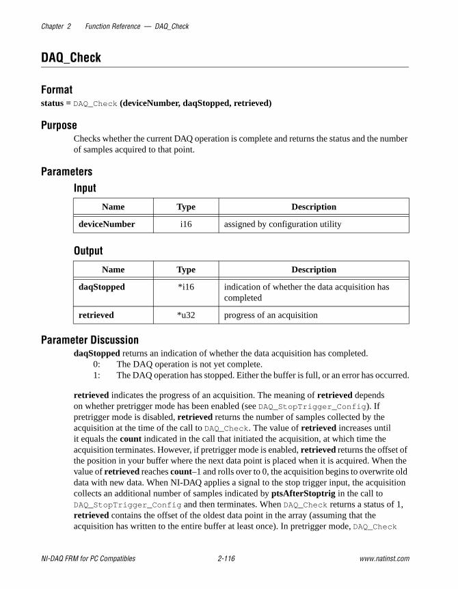
Chapter 2 Function Reference — DAQ_Check
NI-DAQ FRM for PC Compatibles 2-116 www.natinst.com
DAQ_Check
Formatstatus = DAQ_Check (deviceNumber, daqStopped, retrieved)
PurposeChecks whether the current DAQ operation is complete and returns the status and the number of samples acquired to that point.
ParametersInput
Output
Parameter DiscussiondaqStopped returns an indication of whether the data acquisition has completed.
0: The DAQ operation is not yet complete.1: The DAQ operation has stopped. Either the buffer is full, or an error has occurred.
retrieved indicates the progress of an acquisition. The meaning of retrieved depends on whether pretrigger mode has been enabled (see DAQ_StopTrigger_Config ). If pretrigger mode is disabled, retrieved returns the number of samples collected by the acquisition at the time of the call to DAQ_Check. The value of retrieved increases until it equals the count indicated in the call that initiated the acquisition, at which time the acquisition terminates. However, if pretrigger mode is enabled, retrieved returns the offset of the position in your buffer where the next data point is placed when it is acquired. When the value of retrieved reaches count–1 and rolls over to 0, the acquisition begins to overwrite old data with new data. When NI-DAQ applies a signal to the stop trigger input, the acquisition collects an additional number of samples indicated by ptsAfterStoptrig in the call to DAQ_StopTrigger_Config and then terminates. When DAQ_Check returns a status of 1, retrieved contains the offset of the oldest data point in the array (assuming that the acquisition has written to the entire buffer at least once). In pretrigger mode, DAQ_Check
Name Type Description
deviceNumber i16 assigned by configuration utility
Name Type Description
daqStopped *i16 indication of whether the data acquisition has completed
retrieved *u32 progress of an acquisition

Chapter 2 Function Reference — DAQ_Check
© National Instruments Corporation 2-117 NI-DAQ FRM for PC Compatibles
automatically rearranges the array upon completion of the acquisition so that the oldest data point is at the beginning of the array. Thus, retrieved always equals 0 upon completion of a pretrigger mode acquisition.
Note C Programmers—daqStopped and retrieved are pass-by-address parameters.
Using This FunctionDAQ_Check checks the current background DAQ operation to determine whether it has completed and returns the number of samples acquired at the time that you called DAQ_Check. If the operation is complete, DAQ_Check sets daqStopped = 1. Otherwise, daqStopped is set to 0. Before DAQ_Check returns daqStopped = 1, it calls DAQ_Clear , allowing another Start call to execute immediately.
If DAQ_Check returns an overFlowError or an overRunError , the DAQ operation is terminated; some A/D conversions were lost due to a sample rate that is too high (sample interval was too small). An overFlowError indicates that the A/D FIFO memory overflowed because the DAQ servicing operation was not able to keep up with sample rate. An overRunError indicates that the DAQ circuitry was not able to keep up with the sample rate. Before returning either of these error codes, DAQ_Check calls DAQ_Clear to terminate the operation and reinitialize the DAQ circuitry.

Chapter 2 Function Reference — DAQ_Clear
NI-DAQ FRM for PC Compatibles 2-118 www.natinst.com
DAQ_Clear
Formatstatus = DAQ_Clear (deviceNumber)
PurposeCancels the current DAQ operation (both single-channel and multiple-channel scanned) and reinitializes the DAQ circuitry.
ParametersInput
Using This FunctionDAQ_Clear turns off any current DAQ operation (both single-channel and multiple-channel), cancels the background process that is handling the data acquisition, and clears any error flags set as a result of the data acquisition. NI-DAQ then reinitializes the DAQ circuitry so that NI-DAQ can start another data acquisition.
Note If your application calls DAQ_Start , SCAN_Start , or Lab_ISCAN_Start , always make sure that you call DAQ_Clear before your application terminates and returns control to the operating system. Unpredictable behavior can result unless you make this call (either directly, or indirectly through DAQ_Check, Lab_ISCAN_Check , or DAQ_DB_Transfer ).
Name Type Description
deviceNumber i16 assigned by configuration utility

Chapter 2 Function Reference — DAQ_Config
© National Instruments Corporation 2-119 NI-DAQ FRM for PC Compatibles
DAQ_Config
Formatstatus = DAQ_Config (deviceNumber, startTrig, extConv)
PurposeStores configuration information for subsequent DAQ operations.
ParametersInput
Parameter DiscussionstartTrig indicates whether the trigger to initiate DAQ sequences is generated externally.
0: Generate software trigger to start DAQ sequence (the default).1: Wait for external trigger pulse at EXTTRIG of the Lab and 1200 Series devices
to initiate DAQ sequence (not valid for 516 and LPM devices and the DAQCard-500/700).
extConv indicates whether the timing of A/D conversions during the DAQ sequence is controlled externally or internally with the sample-interval and/or scan-interval clocks.
0: Use onboard clock to control data acquisition sample-interval and scan-interval timing (the default).
1: Allow external clock to control sample-interval timing.2: Allow external clock to control scan-interval timing (MIO, AI, and Lab and
1200 Series devices only).3: Allow external control of sample-interval timing and scan-interval timing
(Lab and 1200 Series devices only).
Note If you are using an E Series or DSA device, see the Select_Signal function for information about the external timing signals.
Name Type Description
deviceNumber i16 assigned by configuration utility
startTrig i16 determines whether the trigger to initiate data acquisition is generated externally
extConv i16 selects A/D conversion clock source

Chapter 2 Function Reference — DAQ_Config
NI-DAQ FRM for PC Compatibles 2-120 www.natinst.com
Using This FunctionDAQ_Config saves the parameters in the configuration table for future data acquisition. DAQ_Start and SCAN_Start use the configuration table to set the DAQ circuitry to the correct timing modes.
If both startTrig and extConv are 0, A/D conversions begin as soon as you call DAQ_Start , SCAN_Start , or Lab_ISCAN_Start . When startTrig is 1, A/D conversions do not begin until NI-DAQ receives an external trigger pulse. In the latter case, the Start call merely arms the device. If you are using all E Series devices, see the Select_Signal function for information about the external timing signals. When the A/D conversions have begun (with the start trigger), the onboard counters control the timing of the conversions. When extConv is 1, the timing of A/D conversions is completely controlled by the signal applied at the EXTCONV* input. Again, the Start call merely arms the device, and after you make this call, the device performs an A/D conversion every time NI-DAQ receives a pulse at the EXTCONV* input. When extConv is 2, the device performs a multiple-channel scan each time the device receives an active low pulse at the COUTB1 signal (pin 43) on Lab and 1200 Series devices.
On the E Series, Lab, and 1200 Series devices, you can configure external start triggering and the external sample clock simultaneously.
♦ Lab and 1200 Series devices only:
In most cases, you should not use external conversion pulses in scanning operations when you are using SCXI in Multiplexed mode. There is no way of masking conversions before the data acquisition begins, so any conversion pulses that occur before NI-DAQ triggers the acquisition will advance the SCXI channels.
♦ Lab and 1200 Series devices only:
If the device is using an external timing clock for A/D conversions (extConv = 1), the first clock pulse after one of the three start calls—AI_Setup , DAQ_Start , or Lab_ISCAN_Start —is to activate the device for external timing. It does not generate a conversion. However, all subsequent clock pulses will generate conversions.
♦ E Series devices only:
If you use this function with startTrig = 1, the device waits for an active low external pulse on the PFI0 pin to initiate the DAQ sequence. If you use this function with extConv = 1 or 3, the device uses active low pulses on the PFI2 pin for sample-interval timing. If you use this function with extConv = 2 or 3, the device uses active low pulses on the PFI7 pin for scan-interval timing. You can use the Select_Signal function instead of this function to take advantage of the DAQ-STC signal routing and polarity selection features.

Chapter 2 Function Reference — DAQ_Config
© National Instruments Corporation 2-121 NI-DAQ FRM for PC Compatibles
Note PCI-6110E and PCI-6111E only—The only allowed values for extConv are 0 and 2. The conversions occur simultaneously for all channels and are controlled by the scan interval.
The DSA devices cannot use externally controlled clocks, so extConv is ignored.
The default settings for DAQ modes are as follows:
startTrig = 0: DAQ sequences are initiated through software.
extConv = 0: Onboard clock is used to time A/D conversions.
If you want a DAQ timing configuration different from the default setting, you must call DAQ_Config with the configuration you want before initiating any DAQ sequences. You need to call DAQ_Config only when you change the DAQ configuration from the default setting.
To scan channels on an SCXI-1140 module using an external Track*/Hold signal, you should call DAQ_Config with extConv = 2 so that the Track*/Hold signal of the module can control the scan interval timing during the acquisition.
The configuration information for the analog input circuitry is controlled by the AI_Configure call. This configuration information also affects data acquisition.

Chapter 2 Function Reference — DAQ_DB_Config
NI-DAQ FRM for PC Compatibles 2-122 www.natinst.com
DAQ_DB_Config
Formatstatus = DAQ_DB_Config (deviceNumber, DBmode)
PurposeEnables or disables double-buffered DAQ operations.
ParametersInput
Parameter DiscussionDBmode indicates whether to enable or disable the double-buffered mode of acquisition.
0: Disable double buffering (default).1: Enable double buffering.
Using This FunctionDouble-buffered data acquisition cyclically fills a buffer with acquired data. The buffer is divided into two equal halves so that NI-DAQ can save data from one half while filling the other half. This mechanism makes it necessary to alternately save both halves of the buffer so that NI-DAQ does not overwrite data in the buffer before saving the data. Use the DAQ_DB_Transfer function to save the data as NI-DAQ acquires it. For additional information, see Chapter 5, NI-DAQ Double Buffering, of the NI-DAQ User Manual for PC Compatibles, for more information.
Name Type Description
deviceNumber i16 assigned by configuration utility
DBmode i16 enable or disable double-buffered mode

Chapter 2 Function Reference — DAQ_DB_HalfReady
© National Instruments Corporation 2-123 NI-DAQ FRM for PC Compatibles
DAQ_DB_HalfReady
Formatstatus = DAQ_DB_HalfReady (deviceNumber, halfReady, daqStopped)
PurposeChecks whether the next half buffer of data is available during a double-buffered data acquisition. You can use DAQ_DB_HalfReady to avoid the waiting period that can occur because the double-buffered transfer function (DAQ_DB_Transfer ) waits until the data is ready before retrieving and returning it.
ParametersInput
Output
Parameter DiscussionhalfReady indicates whether the next half buffer of data is available.
0: Data is not yet available.
1: Use DAQ_DB_Transfer to retrieve the data immediately.
daqstopped returns an indication of whether the data acquisition has completed.
0: The DAQ operation is still running.
1: The DAQ operation is complete (or halted due to an error).
Note C Programmers—halfReady and daqStopped are pass-by-address parameters.
Name Type Description
deviceNumber i16 assigned by configuration utility
Name Type Description
halfReady *i16 whether the next half buffer of data is available
daqStopped *i16 whether the data acquisition has completed

Chapter 2 Function Reference — DAQ_DB_HalfReady
NI-DAQ FRM for PC Compatibles 2-124 www.natinst.com
Using This FunctionDouble-buffered data acquisition cyclically fills a buffer with acquired data. The buffer is divided into two equal halves so that NI-DAQ can save data from one half while filling the other half. This mechanism makes it necessary to alternately save both halves of the buffer so that NI-DAQ does not overwrite data in the buffer before saving the data. Use the DAQ_DB_Transfer function to save the data as NI-DAQ acquires it. This function, when called, waits for the data to become available before retrieving it and returning. During slower paced acquisitions this waiting period can be significant. You can use DAQ_DB_HalfReady to ensure that the transfer function is called only when the data is already available.

Chapter 2 Function Reference — DAQ_DB_Transfer
© National Instruments Corporation 2-125 NI-DAQ FRM for PC Compatibles
DAQ_DB_Transfer
Formatstatus = DAQ_DB_Transfer (deviceNumber, halfBuffer, ptsTfr, daqStopped)
PurposeTransfers half of the data from the buffer being used for double-buffered data acquisition to another buffer, which is passed to the function, and waits until the data to be transferred is available before returning. You can execute DAQ_DB_Transfer repeatedly to return sequential half buffers of the data.
ParametersInput
Input/Output
Output
Parameter DiscussionhalfBuffer is an integer array. The size of the array must be at least half the size of the circular buffer being used for double-buffered data acquisition.
ptsTfr is the number of points transferred to halfBuffer . This value is always equal to half the number of samples specified in DAQ_Start , SCAN_Start , or Lab_ISCAN_Start unless the acquisition has not yet begun, or the acquisition stopped while in pretrigger mode. In the former case, until NI-DAQ applies an external start trigger, ptsTfr is zero. In the latter case (pretrigger mode), the acquisition can stop at any point in the circular buffer after acquiring the specified number of samples after the board receives a pulse at stop trigger input, the
Name Type Description
deviceNumber i16 assigned by configuration utility
Name Type Description
halfBuffer [i16] integer array to which the data is to be transferred
Name Type Description
ptsTfr u32 number of points transferred
daqStopped i16 indicates the completion of a pretrigger mode acquisition

Chapter 2 Function Reference — DAQ_DB_Transfer
NI-DAQ FRM for PC Compatibles 2-126 www.natinst.com
EXTTRIG pin of Lab and 1200 Series devices. If you are using all E Series devices, see the Select_Signal function for information about the external timing signals. Thus, after the acquisition has stopped, the last transfer of data to halfBuffer contains the number of valid points from the half of the circular buffer where acquisition stopped.
daqStopped is a valid output parameter only if pretrigger mode acquisition is in progress. This parameter indicates the completion of a pretrigger mode acquisition by returning a one (it returns zero otherwise). A one indicates that the acquisition has stopped after taking the specified number of samples following the occurrence of a stop trigger, and that NI-DAQ has transferred the last piece of data in the circular buffer to halfBuffer . The number of data points transferred to halfBuffer , as always, is equal to ptsTfr .
Note C Programmers—ptsTfr and daqStopped must be passed by reference.
Using this Function Double-buffered data acquisition cyclically fills a buffer with acquired data. The circular buffer is divided into two equal halves so that NI-DAQ can save data from one half while filling the other half. Through the use of a circular buffer, you can collect an unlimited amount of data without requiring an unlimited amount of memory. Double-buffered data acquisition is useful for applications such as writing data to disk and real-time display of data. NI-DAQ can use double-buffered data acquisition for both single-channel and multiple-channel scanned data acquisition. Unless pretrigger mode is in use, you should call DAQ_Clear to stop the continuous cyclical double-buffered acquisition started by DAQ_Start , SCAN_Start , or Lab_ISCAN_Start .
DAQ_DB_Transfer saves to halfBuffer one half of the data from the buffer being used for acquisition. An overWriteBeforeCopy warning is returned by DAQ_DB_Transfer if NI-DAQ has overwritten unretrieved data in the circular buffer. Notice that NI-DAQ transfers the data, even though it returns the warning. Your application might initiate a double-buffered acquisition and then wait for some condition to be satisfied before beginning retrieval of the data. The first call to the DB_Transfer function might return the warning because the circular buffer might have wrapped around at least once since the acquisition started. If subsequent DAQ_DB_Transfer calls keep pace with the acquisition, no further overWriteBeforeCopy warnings should occur.
DAQ_DB_Transfer returns an overwrite error if NI-DAQ overwrites data in the half of the circular buffer being copied to halfBuffer during the transfer. When this error occurs, the data in halfBuffer might be corrupted. Use DAQ_Monitor for very large buffers.

Chapter 2 Function Reference — DAQ_Monitor
© National Instruments Corporation 2-127 NI-DAQ FRM for PC Compatibles
DAQ_Monitor
Formatstatus = DAQ_Monitor (deviceNumber, channel, sequential, numPts, monitorBuffer,
newestPtIndex, daqStopped)
PurposeReturns data from an asynchronous data acquisition in progress. During a multiple-channel acquisition, you can retrieve data from a single channel or from all channels being scanned. An oldest/newest mode provides for return of sequential (oldest) blocks of data or return of the most recently acquired (newest) blocks of data.
ParametersInput
Output
Parameter Discussionchannel is the number of the channel you want to examine. You can choose to set channel to a value of –1 to indicate that you want to examine data from all channels being scanned. If channel is not equal to –1, channel must be equal to the channel selected in DAQ_Start , equal to one of the channels selected in SCAN_Setup, or equal to one of the channels implied
Name Type Description
deviceNumber i16 assigned by configuration utility
channel i16 number of the channel
sequential i16 enables or disables the return of consecutive or oldest blocks of data
numPts u32 number of data points you want to retrieve
Name Type Description
monitorBuffer [i16] destination buffer for the data
newestPtIndex *u32 offset into the acquisition buffer of the newest point returned
daqStopped *i16 indicates whether the data acquisition has completed

Chapter 2 Function Reference — DAQ_Monitor
NI-DAQ FRM for PC Compatibles 2-128 www.natinst.com
in Lab_ISCAN_Start . If you are using an AMUX-64T, channel can be equal to any one of the AMUX-64T channels.Range: –1 for data from all channels being sampled.
n where n is one of the channels being sampled.
sequential is a flag that enables or disables the return of consecutive or oldest blocks of data from the acquisition buffer. A call to DAQ_Monitor with the value of sequential equal to one returns a block of data that begins where the last sequential call to DAQ_Monitor left off. A call to DAQ_Monitor with sequential equal to zero returns the most recent block of data available.
0: Most recent data.1: Consecutive data.
numPts is the number of data points you want to retrieve from the buffer being used by the acquisition operation. If the channel parameter is equal to –1, numPts must be an integer multiple of the number of channels contained in the scan sequence. If you are using one or more AMUX-64T devices, remember that the actual number of channels scanned is equal to the value of the numChans parameter you selected in SCAN_Setup, multiplied by the number of AMUX-64T devices, multiplied by four.Range: (if channel equals –1) one to the value of count in the DAQ_Start , SCAN_Start ,
or Lab_ISCAN_Start call.(if channel is not equal to 1) one to the number of points per channel that the acquisition buffer can hold.
monitorBuffer is the destination buffer for the data. It is an integer array. monitorBuffer must be at least big enough to hold numPts worth of data. Upon the return of DAQ_Monitor , monitorBuffer contains a snapshot of a portion of the acquisition buffer.
newestPtIndex is the offset into the acquisition buffer of the newest point returned by DAQ_Monitor . When the value of the sequential flag is 0, newestPtIndex is useful in determining whether you are seeing the same data over and over again. If DAQ_buffer is the name of the buffer selected in the DAQ_Start call, for example, monitorBuffer [numPts – 1] = DAQ_buffer [newestPtIndex], if DAQ_buffer is zero based.
daqStopped returns an indication of whether the data acquisition has completed.0: The DAQ operation is not yet complete.1: The DAQ operation has completed (or halted due to an error).
Note C Programmers—newestPtIndex and daqStopped are pass-by-address parameters.

Chapter 2 Function Reference — DAQ_Monitor
© National Instruments Corporation 2-129 NI-DAQ FRM for PC Compatibles
Using This FunctionDAQ_Monitor is intended to return small blocks of data from a background acquisition operation. This is especially useful when you have put the acquisition in a circular mode by enabling either the double-buffered or pretrigger modes. The operation is not disturbed; NI-DAQ only reads data from the buffer being used by the acquisition. If the amount of data requested is not yet available, DAQ_Monitor returns the appropriate error code. Possible uses for DAQ_Monitor include deciding when to halt an acquisition based on a level, slope, or peak. If you are using DAQ_Monitor to retrieve sequential data (during a circular acquisition) and NI-DAQ overwrites a block of data before it can copy the data, NI-DAQ returns an overWriteError warning. DAQ_Monitor then restarts sequential retrieval with the most recently acquired block of data. DAQ_Monitor is also useful for returning data from huge buffers because it is not restricted to one-half of the circular buffer size, unlike DAQ_DB_Transfer .
If NI-DAQ overwrites a block of data as it is copied to monitorBuffer , NI-DAQ returns the overWriteError error. The data in monitorBuffer might be corrupted if NI-DAQ returns this error.

Chapter 2 Function Reference — DAQ_Op
NI-DAQ FRM for PC Compatibles 2-130 www.natinst.com
DAQ_Op
Formatstatus = DAQ_Op (deviceNumber, chan, gain, buffer, count, sampleRate)
PurposePerforms a synchronous, single-channel DAQ operation. DAQ_Op does not return until NI-DAQ has acquired all the data or an acquisition error has occurred.
ParametersInput
Input/Output
Parameter Discussionchan is the analog input channel number. If you are using SCXI, you must use the appropriate analog input channel on the DAQ device that corresponds to the SCXI channel you want. Select the SCXI channel using SCXI_Single_Chan_Setup before calling this function. Refer to the NI-DAQ User Manual for PC Compatibles for more information on SCXI channel assignments.Range: See Table B-1, Valid Analog Input Channel Settings, in Appendix B, Analog
Input Channel, Gain Settings, and Voltage Calculation.
gain is the gain setting to be used for that channel. This gain setting applies only to the DAQ device; if you are using SCXI, you must establish any gain you want at the SCXI module by setting jumpers on the module or by calling SCXI_Set_Gain . Refer to Appendix B, Analog Input Channel, Gain Settings, and Voltage Calculation, for valid gain settings. If you use an
Name Type Description
deviceNumber i16 assigned by configuration utility
chan i16 analog input channel number
gain i16 gain setting to be used
count u32 number of samples to be acquired
sampleRate f64 desired sample rate in units of pts/s
Name Type Description
buffer [i16] conversion samples returned

Chapter 2 Function Reference — DAQ_Op
© National Instruments Corporation 2-131 NI-DAQ FRM for PC Compatibles
invalid gain, NI-DAQ returns an error. NI-DAQ ignores gain for 516 and LPM devices and the DAQCard-500/700.
buffer is an integer array. buffer has a length equal to or greater than count. When DAQ_Op returns with an error number equal to zero, buffer contains the acquired data.
count is the number of samples to be acquired (that is, the number of A/D conversions to be performed). Range: 3 through 232 – 1 (except for the Lab and 1200 Series and E Series devices).
3 through 65,535 (Lab and 1200 Series devices).2 through 224 (E Series devices).2 through 224 – 3 (PCI-6110E and PCI-6111E) requires an even number of samples.2 through 224 – 1 (445X devices).2 through 232 – 1 (455X devices).
sampleRate is the sample rate you want in, units of pts/s.Range: Roughly 0.00153 pts/s through 5,000,000 pts/s. The maximum rate depends on
the type of device.
Note If you are using an SCXI-1200 with remote SCXI, the maximum rate depends on the baud rate setting and count. Refer to the SCXI-1200 User Manual for more details.
Using This FunctionDAQ_Op initiates a synchronous process of acquiring A/D conversion samples and storing them in a buffer. DAQ_Op does not return control to your application until NI-DAQ acquires all the samples you want (or until an acquisition error occurs). When you are using posttrigger mode (with pretrigger mode disabled), the process stores count A/D conversions in the buffer and ignores any subsequent conversions.
Note If you have selected external start triggering of the DAQ operation, a low-to-high edge at the EXTTRIG input of the Lab and 1200 Series devices initiates the DAQ operation. If you are using an E Series device or DSA device, you need to apply a trigger that you select through the Select_Signal or DAQ_Config functions to initiate data acquisition. Be aware that if you do not apply the start trigger, DAQ_Op does not return control to your application. Otherwise, DAQ_Op issues a software trigger to initiate the DAQ operation.

Chapter 2 Function Reference — DAQ_Op
NI-DAQ FRM for PC Compatibles 2-132 www.natinst.com
If you have enabled pretrigger mode, the sample counter does not begin counting acquisitions until you apply a signal at the stop trigger input. Until you apply this signal, the acquisition remains in a cyclical mode, continually overwriting old data in the buffer with new data. Again, if you do not apply the stop trigger, DAQ_Op does not return control to your application.
In any case, you can use Timeout_Config to establish a maximum length of time for DAQ_Op to execute.

Chapter 2 Function Reference — DAQ_Rate
© National Instruments Corporation 2-133 NI-DAQ FRM for PC Compatibles
DAQ_Rate
Formatstatus = DAQ_Rate (rate, units, timebase, sampleInterval)
PurposeConverts a DAQ rate into the timebase and sample-interval values needed to produce the rate you want.
ParametersInput
Output
Parameter Discussionrate is the DAQ rate you want. The units in which rate is expressed are either points per second (pts/s) or seconds per point (s/pt), depending on the value of the units parameter.Range: Roughly 0.00153 pts/s through 5,000,000 pts/s or 655 s/pt through 0.000001 s/pt.
units indicates the units used to express rate.0: points per second.1: seconds per point.
timebase is a code representing the resolution of the onboard clock signal that the device uses to produce the acquisition rate you want. You can input the value returned by timebase directly to DAQ_Start , Lab_ISCAN_Start , or SCAN_Start . timebase has the following possible values:
–3: 20 MHz clock used as the timebase (50 ns) (E Series only).–1: 200 ns (E Series devices only).1: 1 µs.
Name Type Description
rate f64 desired DAQ rate
units i16 pts/s or s/pt (see CTR_Rate)
Name Type Description
timebase *i16 onboard source signal used
sampleInterval *u16 number of timebase units that elapse between consecutive A/D conversions

Chapter 2 Function Reference — DAQ_Rate
NI-DAQ FRM for PC Compatibles 2-134 www.natinst.com
2: 10 µs.3: 100 µs.4: 1 ms.5: 10 ms.
sampleInterval is the number of timebase units that elapse between consecutive A/D conversions. The combination of the timebase resolution value and the sampleInterval produces the DAQ rate you want.Range: 2 through 65,535.
Note C Programmers—timebase and sampleInterval are pass-by-address parameters.
Using This FunctionDAQ_Rate produces timebase and sample-interval values to closely match the DAQ rate you want. To calculate the actual acquisition rate produced by these values, first determine the clock resolution that corresponds to the value timebase returns. Then use the appropriate formula, depending on the value specified for units.
units = 0 (pts/s):
actual rate = 1/(clock resolution * sampleInterval)
units = 1 (s/pt):
actual rate = clock resolution * sampleInterval

Chapter 2 Function Reference — DAQ_Set_Clock
© National Instruments Corporation 2-135 NI-DAQ FRM for PC Compatibles
DAQ_Set_Clock
Formatstatus = DAQ_Set_Clock (deviceNumber, group, whichClock, desiredRate, units, actualRate)
PurposeSets the scan rate for a group of channels (DSA devices only).
Input
Output
Parameter DiscussionwhichClock indicates the type of clock.
0: scan clock.
desiredRate is the rate at which you want data points to be sampled by the ADC(s).
units determines how desiredRate and actualRate are interpreted.0: points per second.1: seconds per point.
actualRate is the rate at which the ADCs produce samples. The capabilities of your device will determine how closely actualRate matches desiredRate. The DSA devices use the same base clock for both DAQ/SCAN and WFM operations so the rates available for a DAQ/SCAN will be restricted if a WFM operation is already in progress.
Note C programmers—actualRate is a pass-by-address parameter.
Name Type Description
deviceNumber i16 assigned by configuration utility
whichClock u32 only scan clock supported
desiredRate f64 desired rate in units
units u32 ticks/second or seconds/tick
Name Type Description
actualRate *f64 actual rate in units

Chapter 2 Function Reference — DAQ_Set_Clock
NI-DAQ FRM for PC Compatibles 2-136 www.natinst.com
Using This FunctionDAQ_Set_Clock sets the specified clock rate for the next acquisition operation. Be sure to call DAQ_Set_Clock before DAQ_Start or SCAN_Start . When calling those functions, the timebase and interval parameters will be ignored.

Chapter 2 Function Reference — DAQ_Start
© National Instruments Corporation 2-137 NI-DAQ FRM for PC Compatibles
DAQ_Start
Formatstatus = DAQ_Start (deviceNumber, chan, gain, buffer, count, timebase, sampInterval)
PurposeInitiates an asynchronous, single-channel DAQ operation and stores its input in an array.
Input
Input/Output
Parameter Discussionchan is the analog input channel number. If you are using SCXI, you must use the appropriate analog input channel on the DAQ device that corresponds to the SCXI channel you want. Select the SCXI channel using SCXI_Single_Chan_Setup before calling this function. Refer to the NI-DAQ User Manual for PC Compatibles for more information on SCXI channel assignments.Range: See Table B-1, Valid Analog Input Channel Settings, in Appendix B, Analog
Input Channel, Gain Settings, and Voltage Calculation.
gain is the gain setting to be used for that channel. This gain setting applies only to the DAQ device; if you are using SCXI, you must establish any gain you want at the SCXI module either by setting jumpers on the module or by calling SCXI_Set_Gain . Refer to Appendix B, Analog Input Channel, Gain Settings, and Voltage Calculation, for valid gain settings. If you
Name Type Description
deviceNumber i16 assigned by configuration utility
chan i16 analog input channel number
gain i16 gain setting
count u32 number of samples that buffer can hold at any given time.
timebase i16 timebase value
sampInterval u16 sample interval
Name Type Description
buffer [i16] conversion samples returned
Chapter 2 Function Reference — DAQ_Start
NI-DAQ FRM for PC Compatibles 2-138 www.natinst.com
use invalid gain settings, NI-DAQ returns an error. NI-DAQ ignores gain for the 516 and LPM devices and DAQCard-500/700.
buffer is an integer array. buffer must have a length equal to or greater than count. The elements of buffer are the results of each A/D conversion in the DAQ operation. This buffer is often referred to as the acquisition buffer (or circular buffer when double-buffered mode is enabled) elsewhere in this manual.
For DSA devices, buffer should be an array of type i32. These devices return the data in a 32-bit format in which the data bits are in the most significant bits.
count is the number of unique samples that buffer can hold at any given time. In a single-buffered acquisition, count actually corresponds to the size (in number of samples) that the DAQ device will acquire. In a double-buffered acquisition, count corresponds to the size (in number of samples) of buffer (acquisition buffer) that will be filled up in a circular fashion. It must also be even.Range: 3 through 232 – 1 (except Lab and 1200 Series devices that are not enabled for
doubled-buffered mode and the E Series devices).3 through 65,535 (Lab and 1200 Series devices not enabled for double-buffered mode).2 through 224 – 1 (E Series devices).2 through 224 – 4 (PCI-6110E and PCI-6111E). count must always be EVEN.2 through 224 – 1 (445X devices).2 through 232 – 1 (455X devices).
timebase is the timebase, or resolution, to be used for the sample-interval counter. timebase has the following possible values:
–3: 20 MHz clock used as a timebase (50 ns) (E Series only).–1: 5 MHz clock used as timebase (200 ns resolution).0: External clock used as timebase (connect your own timebase frequency to the
internal sample-interval counter via the default PFI8 input for E Series devices).1: 1 MHz clock used as timebase (1 µs resolution). 2: 100 kHz clock used as timebase (10 µs resolution).3: 10 kHz clock used as timebase (100 µs resolution). 4: 1 kHz clock used as timebase (1 ms resolution). 5: 100 Hz clock used as timebase (10 ms resolution).
On E Series devices, if you use this function with the timebase set to 0, you must call the function Select_Signal with signal set to ND_IN_SCAN_CLOCK_TIMEBASE (not ND_IN_CHANNEL_CLOCK_TIMEBASE), and source set to a value other than ND_INTERNAL_20_MHZ and ND_INTERNAL_100_KHZ before calling DAQ_Start with timebase set to 0; otherwise, DAQ_Start selects low-to-high transitions on the PFI 8 I/O connector pin as your external timebase.

Chapter 2 Function Reference — DAQ_Start
© National Instruments Corporation 2-139 NI-DAQ FRM for PC Compatibles
Refer to the Select_Signal function for further details about using the timebase with E Series devices.
If you use external conversion pulses, NI-DAQ ignores the timebase parameter and you can set it to any value.
For DSA devices, timebase is ignored. Use DAQ_Set_Clock to set the sampling rate.
sampInterval indicates the length of the sample interval (that is, the amount of time to elapse between each A/D conversion).Range: 2 through 65,535.
The sample interval is a function of the timebase resolution. NI-DAQ determines the actual sample interval in seconds using the following formula:
sampInterval * (timebase resolution)
where the timebase resolution for each value of timebase is given above. For example, if sampInterval = 25 and timebase = 2, the sample interval is 25 * 10 µs = 250 µs. If you use external conversion pulses, NI-DAQ ignores the sampInterval parameter and you can set it to any value.
For DSA devices, sampInterval is ignored. Use DAQ_Set_Clock to set the sampling rate.
Note If you are using an SCXI-1200 with remote SCXI, the maximum rate depends on the baud rate setting and count. Refer to the SCXI-1200 User Manual for more details.
Using This FunctionDAQ_Start configures the analog input multiplexer and gain circuitry as indicated by chan and gain. If external sample-interval timing has not been indicated by a DAQ_Config call, the function sets the sample-interval counter to the specified sampInterval and timebase. If you have indicated external sample-interval timing, the DAQ circuitry relies on pulses received on the external conversion signal EXTCONV* input to initiate individual A/D conversions. The sample counter is set up to count the number of samples and to stop the DAQ process when NI-DAQ has acquired count samples.
DAQ_Start initializes a background process to handle storing of A/D conversion samples into the buffer as NI-DAQ acquires the conversions. When you use posttrigger mode (with pretrigger mode disabled), the process stores up to count A/D conversions in the buffer and ignores any subsequent conversions. If a call to DAQ_Check returns status = 1, the samples are available and NI-DAQ terminates the DAQ process. In addition, a call to DAQ_Clear terminates the background DAQ process and enables a subsequent call to DAQ_Start . Notice that if DAQ_Check returns daqStopped = 1 or an error code of overRunError or overFlowError , the process is automatically terminated and there is no need to call DAQ_Clear .

Chapter 2 Function Reference — DAQ_Start
NI-DAQ FRM for PC Compatibles 2-140 www.natinst.com
Note You need to apply a trigger that you select through the Select_Signal or DAQ_Config functions to initiate data acquisition.
If you select external start triggering for the DAQ operation, a low-to-high edge at the EXTTRIG input of Lab and 1200 Series devices initiates the DAQ operation after the DAQ_Start call is complete. If you are using an E Series or DSA device, you need to apply a trigger that you select through the Select_Signal or DAQ_Config functions to initiate data acquisition. Otherwise, DAQ_Start issues a software trigger to initiate the DAQ operation before returning.
If you enable pretrigger mode, the sample counter does not begin counting acquisitions until a signal is applied at the stop trigger input. Until this signal is applied, the acquisition remains in a cyclical mode, continually overwriting old data in the buffer with new data.
Note If your application calls DAQ_Start , SCAN_Start , or Lab_ISCAN_Start , always make sure that you call DAQ_Clear before your application terminates and returns control to the operating system. Unpredictable behavior can result unless you make this call (either directly, or indirectly through DAQ_Check or DAQ_DB_Transfer ) .

Chapter 2 Function Reference — DAQ_StopTrigger_Config
© National Instruments Corporation 2-141 NI-DAQ FRM for PC Compatibles
DAQ_StopTrigger_Config
Formatstatus = DAQ_StopTrigger_Config (deviceNumber, stopTrig, ptsAfterStoptrig)
PurposeEnables the pretrigger mode of data acquisition and indicates the number of data points to acquire after the stop trigger pulse is applied at the EXTTRIG input of Lab and 1200 Series devices; or the PFI1 pin of an E Series device. If you are using an E Series device, see the Select_Signal description for information about the external timing signals.
ParametersInput
Parameter DiscussionstopTrig indicates whether to enable or disable the pretriggered mode of data acquisition.
0: Disable pretrigger (the default).1: Enable pretrigger.
ptsAfterStoptrig is the number of data points to acquire after the trigger. This parameter is valid only if stopTrig equals 1. For a multiple channel scanned acquisition, ptsAfterStoptrig must be an integer multiple of the number of channels scanned.Range: 3 through count, where count is the value of the count parameter in the Start call
used to start the acquisition. For Lab and 1200 Series devices, the maximum is always 65,535. For an E Series device or DSA device, the range is 2 through count. Additionally for E Series devices, the number of scans acquired after the stop trigger must be at least 2. The number of scans is equal to the count divided by the total number of channels scanned.
Using This FunctionCalling DAQ_StopTrigger_Config with the stopTrig parameter set to 1 causes any subsequent Start call to initiate a cyclical mode data acquisition. In this mode, NI-DAQ writes data continually into your buffer, overwriting data at the beginning of the buffer when NI-DAQ has filled the entire buffer. You can use DAQ_Check or Lab_ISCAN_Check in this situation to determine where NI-DAQ is currently depositing data in the buffer. When a pulse
Name Type Description
deviceNumber i16 assigned by configuration utility
stopTrig i16 enable or disable the pretriggered mode
ptsAfterStoptrig u32 number of points to acquire after the trigger

Chapter 2 Function Reference — DAQ_StopTrigger_Config
NI-DAQ FRM for PC Compatibles 2-142 www.natinst.com
is applied at the EXTTRIG input of Lab and 1200 Series devices, NI-DAQ acquires an additional number of data points specified by ptsAfterStoptrig before the acquisition terminates. DAQ_Check or Lab_ISCAN_Check rearranges the data into chronological order (from oldest to newest) and returns with the status parameters equal to one when called after termination.
Calling DAQ_StopTrigger_Config with stopTrig set to 0 returns the acquisition mode to its default, acyclical setting.
(E Series devices only) If you use this function with stopTrig = 1, the device uses an active high signal from the PFI1 pin as the stop trigger. After calling this function, you can use the Select_Signal function to take advantage of the DAQ-STC signal routing and polarity selection features.

Chapter 2 Function Reference — DAQ_to_Disk
© National Instruments Corporation 2-143 NI-DAQ FRM for PC Compatibles
DAQ_to_Disk
Formatstatus = DAQ_to_Disk (deviceNumber, chan, gain, filename, count, sampleRate, concat)
PurposePerforms a synchronous, single-channel DAQ operation and saves the acquired data in a disk file. DAQ_to_Disk does not return until NI-DAQ has acquired and saved all the data or an acquisition error has occurred.
ParametersInput
Parameter Discussionchan is the analog input channel number. If you are using SCXI, you must use the appropriate analog input channel on the DAQ device that corresponds to the SCXI channel you want. Select the SCXI channel using SCXI_Single_Chan_Setup before calling this function. Refer to the NI-DAQ User Manual for PC Compatibles for more information on SCXI channel assignments.Range: See Table B-1, Valid Analog Input Channel Settings, in Appendix B, Analog
Input Channel, Gain Settings, and Voltage Calculation.
gain is the gain setting to be used for that channel. This gain setting applies only to the DAQ device; if SCXI is used, you must establish any gain at the SCXI module either by setting jumpers on the module or by calling SCXI_Set_Gain . Refer to Appendix B, Analog Input Channel, Gain Settings, and Voltage Calculation, for valid gain settings. If you use invalid gain settings, NI-DAQ returns an error. NI-DAQ ignores gain for 516 and LPM devices and the DAQCard-500/700.
Name Type Description
deviceNumber i16 assigned by configuration utility
chan i16 analog input channel number
gain i16 gain setting
filename STR name of data file to be created
count u32 number of samples to be acquired
sampleRate f64 rate in units of pts/s
concat i16 enables concatenation to an existing file
Chapter 2 Function Reference — DAQ_to_Disk
NI-DAQ FRM for PC Compatibles 2-144 www.natinst.com
count is the number of samples to be acquired (that is, the number of A/D conversions to be performed). The length of your data file in bytes should be exactly twice the value of count upon completion of the acquisition. If you have previously enabled pretrigger mode (by a call to DAQ_StopTrigger_Config ), NI-DAQ ignores the count parameter.Range: 3 through 232 – 1 (except the E Series devices).
2 through 224 (E Series devices).2 through 224 – 3 (PCI-6110E and PCI-6111E), count must be EVEN.2 through 224 (445X devices).2 through 232 – 1 (455X devices).
sampleRate is the sample rate you want in units of points per second.Range: Roughly 0.00153 pts/s through 5,000,000 pts/s. The maximum range varies
according to the type of device you have and the speed and degree of fragmentation of your disk storage device.
Note If you are using an SCXI-1200 with remote SCXI, the maximum rate depends on the baud rate setting and count. Refer to the SCXI-1200 User Manual for more details.
concat enables concatenation of data to an existing file. Regardless of the value of concat, if the file does not exist, it is created.
0: Overwrite file if it exists.1: Concatenate new data to an existing file.
Using This FunctionDAQ_to_Disk initiates a synchronous process of acquiring A/D conversion samples and storing them in a disk file. Data is written to disk in 16-bit binary format, with the lower byte first (little endian). DAQ_to_Disk does not return control to your application until NI-DAQ acquires and saves all the samples you want (or until an acquisition error occurs).
Note If you select external start triggering for the DAQ operation, a low-to-high edge at the EXTTRIG input of Lab and 1200 Series devices initiates the DAQ operation. If you are using an E Series device, you need to apply a trigger that you select through the Select_Signal or DAQ_Config functions to initiate data acquisition. If you are using E Series devices, see the Select_Signal function for information about the external timing signals. Be aware that if you do not apply the start trigger, DAQ_to_Disk does not return control to your application. Otherwise, DAQ_to_Disk issues a software trigger to initiate the DAQ operation.

Chapter 2 Function Reference — DAQ_to_Disk
© National Instruments Corporation 2-145 NI-DAQ FRM for PC Compatibles
If you enable pretrigger mode, the sample counter does not begin counting acquisitions until you apply a signal at the stop trigger input. Until you apply this signal, the acquisition continues to write data into the disk file. NI-DAQ ignores the value of the count parameter when you enable pretrigger mode. If the stop trigger is not applied, DAQ_to_Disk eventually returns control to your application because, you eventually run out of disk space.
In any case, you can use Timeout_Config to establish a maximum length of time for DAQ_to_Disk to execute.

Chapter 2 Function Reference — DAQ_VScale
NI-DAQ FRM for PC Compatibles 2-146 www.natinst.com
DAQ_VScale
Formatstatus = DAQ_VScale (deviceNumber, chan, gain, gainAdjust, offset, count, binArray, voltArray)
PurposeConverts the values of an array of acquired binary data and the gain setting for that data to actual input voltages measured.
ParametersInput
Output
Parameter Discussionchan is the onboard channel or AMUX channel on which the binary data was acquired. For devices other than the E Series devices and DSA devices, this parameter is ignored because the scaling calculation is the same for all of the channels. However, you are encouraged to pass the correct channel number.
gain is the gain setting at which NI-DAQ acquired the data in binArray . If you used SCXI to take the reading, this gain parameter should be the product of the gain on the SCXI module channel and the gain used by the DAQ device.
Name Type Description
deviceNumber i16 assigned by configuration utility
chan i16 channel on which binary reading was taken
gain i16 gain setting
gainAdjust f64 multiplying factor to adjust gain
offset f64 binary offset present in reading
count u32 length of binArray and voltArray
binArray [i16] acquired binary data
Name Type Description
voltArray [f64] double-precision values returned

Chapter 2 Function Reference — DAQ_VScale
© National Instruments Corporation 2-147 NI-DAQ FRM for PC Compatibles
gainAdjust is the multiplying factor to adjust the gain. Refer to Appendix B, Analog Input Channel, Gain Settings, and Voltage Calculation, for the procedure for determining gainAdjust. If you do not want to do any gain adjustment, (for example, the ideal gain as specified by the parameter gain) you must set gainAdjust to 1.
offset is the binary offset that needs to be subtracted from reading. Refer to Appendix B, Analog Input Channel, Gain Settings, and Voltage Calculation, for the procedure for determining offset. If you do not want to do any offset compensation, offset must be set to 0. The data type is double to allow for offset fractional least significant bits (LSB). For example, you could use DAQ_Op to acquire many samples from a grounded input channel and average them to obtain the offset.
binArray is an array of acquired binary data.
For DSA devices, binArray should be an array of i32.
voltArray is an array of double-precision values returned by DAQ_VScale and is the voltage representation of binArray .
Using This FunctionRefer to Appendix B, Analog Input Channel, Gain Settings, and Voltage Calculation, for the formula used by DAQ_VScale to calculate voltage from binary reading.

Chapter 2 Function Reference — DIG_Block_Check
NI-DAQ FRM for PC Compatibles 2-148 www.natinst.com
DIG_Block_Check
Formatstatus = DIG_Block_Check (deviceNumber, group, remaining)
PurposeReturns the number of items remaining to be transferred after a DIG_Block_In or DIG_Block_Out call.
ParametersInput
Output
Parameter Discussiongroup is the group involved in the asynchronous transfer.Range: 1 or 2 for most devices.
1 through 8 for the DIO-96.
remaining is the number of items yet to be transferred. The actual number of bytes remaining to be transferred is equal to remaining multiplied by the value of groupSize specified in the call to DIG_Grp_Config or DIG_SCAN_Setup .
Note C Programmers—remaining is a pass-by-address parameter.
Using This FunctionDIG_Block_Check monitors an asynchronous transfer of data started via a DIG_Block_In or DIG_Block_Out call. If NI-DAQ has completed the transfer, DIG_Block_Check automatically calls DIG_Block_Clear , which permits NI-DAQ to make a new block transfer call immediately.
Name Type Description
deviceNumber i16 assigned by configuration utility
group i16 group
Name Type Description
remaining *u32 number of items yet to be transferred

Chapter 2 Function Reference — DIG_Block_Clear
© National Instruments Corporation 2-149 NI-DAQ FRM for PC Compatibles
DIG_Block_Clear
Formatstatus = DIG_Block_Clear (deviceNumber, group)
PurposeHalts any ongoing asynchronous transfer, allowing another transfer to be initiated.
ParametersInput
Parameter Discussiongroup is the group involved in the asynchronous transfer.Range: 1 or 2 for most devices.
1 through 8 for the DIO-96.
Using This Function(AT-DIO-32F only) If you aligned the buffer that you used in the previous call to DIG_Block_Out or DIG_Block_In by a call to Align_DMA_Buffer , DIG_Block_Clear unaligns that buffer before returning. Unaligning a buffer means that the data is shifted so that the first data point is located at buffer [0].
After NI-DAQ has started a block transfer, you must call DIG_Block_Clear before NI-DAQ can initiate another block transfer. Notice that DIG_Block_Check makes this call for you when it sees that NI-DAQ has completed a transfer. DIG_Block_Clear does not change any current group assignments, alter the current handshaking settings, or affect the state of the pattern generation mode.
Name Type Description
deviceNumber i16 assigned by configuration utility
group i16 group

Chapter 2 Function Reference — DIG_Block_In
NI-DAQ FRM for PC Compatibles 2-150 www.natinst.com
DIG_Block_In
Formatstatus = DIG_Block_In (deviceNumber, group, buffer, count)
PurposeInitiates an asynchronous transfer of data from the specified group to memory.
ParametersInput
Input/Output
Parameter Discussiongroup is the group to be read from.Range: 1 or 2 for most devices.
1 through 8 for DIO-96.
buffer is an integer array that contains the data obtained by reading the group indicated by group. For the DIO-32F and DIO 6533 (DIO-32HS), NI-DAQ uses all 16 bits in each buffer element. Therefore, the size of the array, in bytes, must be at least count multiplied by the size of group. For all other devices, only the lower 8 bits of each buffer element are used. Therefore, the size of the array in bytes must be at least twice count multiplied by the size of group.
count is the number of items (for example, 8-bit items for a group of size 1, 16-bit items for a group of size 2, and 32-bit items for a group of size 4) to be transferred to the area of memory specified by buffer from the group indicated by group.Range: 2 through 232 – 1.
Name Type Description
deviceNumber i16 assigned by configuration utility
group i16 group
count u32 number of items to be transferred
Name Type Description
buffer [i16] conversion samples returned

Chapter 2 Function Reference — DIG_Block_In
© National Instruments Corporation 2-151 NI-DAQ FRM for PC Compatibles
Using This FunctionDIG_Block_In initiates an asynchronous transfer of data from a specified group to your buffer. The hardware is responsible for the handshaking details. Call DIG_Grp_Config for the DIO-32F and the DIO 6533 (DIO-32HS), or DIG_SCAN_Setup for all other devices at least once before calling DIG_Block_In . DIG_Grp_Config and DIG_SCAN_Setup select the group configuration for handshaking.
If you use a DIO-32F or DIO 6533 (DIO-32HS), DIG_Block_In writes data to all bytes of your buffer regardless of the group size. If the group size is 1 (which is supported only by the DIO 6533), DIG_Block_In writes to the lower 8 bits of buffer [0] on the first read from the group and the upper 8 bits of buffer [0] on the second read from the group. For example, if the first read acquired is 0xCD and the second data acquired is 0xAB, buffer [0] is 0xABCD. If group size is 2, DIG_Block_In writes data from the lower port (port 0 or port 2) to the lower 8 bits of buffer [0] and data from the higher port (port 1 or port 3) to the upper eight bits of buffer [0]. If group size is 4, DIG_Block_In writes the data from ports 0 and 1 to buffer [0] and the data from ports 2 and 3 to buffer [1].
Note On the DIO-32F, you cannot use DIG_Block_In with a group of size= 1. On the DIO 6533, you can use DIG_Block_In with a group ofsize = 1, but count must be even in this case.
If you use any device but a DIO-32F or DIO 6533, NI-DAQ writes to the lower byte of each buffer element with a value read from the group and sets the upper byte of each buffer element to zero. If the group size is 2, the lower byte of buffer [0] receives data from the first port in the group and the lower byte of buffer [1] receives data from the second port. NI-DAQ sets the upper bytes of buffer [0] and buffer [1] to 0.
If you have not configured the specified group as an input group, NI-DAQ does not perform the operation and returns an error. If you have assigned no ports to the specified group, NI-DAQ does not perform the operation and returns an error. You can call DIG_Block_Check to monitor the status of a transfer initiated by DIG_Block_In .
If previously enabled, pattern generation for the DIO-32F or the DIO 6533 begins when you execute DIG_Block_In . See Pattern Generation I/O with the DIO-32F and DIO 6533 (DIO-32HS) Devices in Chapter 3, Software Overview, of the your NI-DAQ User Manual for PC Compatibles for important information about pattern generation.
To avoid delays that are caused by AT-bus DMA reprogramming on an AT-DIO-32F or AT-DIO-32HS, you can use dual DMA, or you can align your buffer. For more information about dual DMA, see the Set_DAQ_Device_Info function. The second option, aligning your buffer, works only for the AT-DIO-32F with buffers up to 64K in size.

Chapter 2 Function Reference — DIG_Block_In
NI-DAQ FRM for PC Compatibles 2-152 www.natinst.com
For the AT-DIO-32F, you can align your buffer by calling Align_DMA_Buffer . If you have aligned your buffer with a call to Align_DMA_Buffer and have not called DIG_Block_Clear (either directly or through DIG_Block_Check ) to unalign the data, you must use the value of alignIndex return by Align_DMA_Buffer to access your data. In other words, data in an aligned buffer begins at buffer[alignIndex] . Data in an unaligned buffer begins at buffer [0].
Note DIG_Block_In will not work with groups of size = 1, because of a DMA limitation when using the AT-DIO-32F.
Note If you are using an SCXI-1200 with remote SCXI, count is limited by the amount of memory made available on the remote SCXI unit. For digital buffered input, you are limited to 5,000 bytes of data. The upper bound for count depends on the groupSize set in DIG_SCAN_Setup (for example, if groupSize = 2, count ≤ 2,500).

Chapter 2 Function Reference — DIG_Block_Out
© National Instruments Corporation 2-153 NI-DAQ FRM for PC Compatibles
DIG_Block_Out
Formatstatus = DIG_Block_Out (deviceNumber, group, buffer, count)
PurposeInitiates an asynchronous transfer of data from memory to the specified group.
ParametersInput
Parameter Discussiongroup is the group to be written to.Range: 1 or 2 for most devices.
1 through 8 for DIO-96.
buffer is an integer array containing your data. NI-DAQ writes the data in this array to the group indicated by group. For the DIO-32F and DIO 6533 (DIO-32HS) devices, NI-DAQ uses all 16 bits in each buffer element. Therefore, the size of the array, in bytes, must be at least count multiplied by the size of group. For all other devices, NI-DAQ uses only the lower 8 bits of each buffer element. Therefore, the size of the array, in bytes, must be at least twice count multiplied by the size of group.
count is the number of items (for example, 8-bit items for a group of size 1, 16-bit items for a group of size 2, and 32-bit items for a group of size 4) to be transferred from the area of memory specified by buffer to the group indicated by group.Range: 2 through 232 – 1.
Using This FunctionDIG_Block_Out initiates an asynchronous transfer of data from your buffer to a specified group. The hardware is responsible for the handshaking details. Call DIG_Grp_Config for the DIO-32F and the DIO 6533 devices, or DIG_SCAN_Setup for the other devices at least once before calling DIG_Block_Out to select the group configuration for handshaking.
Name Type Description
deviceNumber i16 assigned by configuration utility
group i16 group
buffer [i16] array containing the user’s data
count u32 number of items to be transferred

Chapter 2 Function Reference — DIG_Block_Out
NI-DAQ FRM for PC Compatibles 2-154 www.natinst.com
If you use a DIO-32F or a DIO 6533 (DIO-32HS), NI-DAQ writes all bytes in your buffer to the group regardless of the group size. If the group size is one (which is supported only by the DIO 6533), DIG_Block_Out writes the lower 8 bits of buffer [0] to the group on the first write and the upper 8 bits of buffer [0] to the group on the second write. For example, if buffer [0] = 0xABCD, NI-DAQ writes 0xCD to the group on the first write, and writes 0xAB to the group on the second write. If group size is 2, DIG_Block_Out writes data from the lower 8 bits of buffer [0] to the lower port (port 0 or port 2) and data from the upper 8 bits of buffer [0] to the higher port (port 1 or port 3). If group size is 4, DIG_Block_Out writes data from buffer [0] to ports 0 and 1 and data from buffer [1] to ports 2 and 3.
If you use any device but a DIO-32F or a DIO 6533 (DIO-32HS), NI-DAQ writes the lower byte of each buffer element to the group in the order indicated in portList when you call DIG_SCAN_Setup . If the group size is 2, on the first write DIG_Block_Out writes the lower byte of buffer [0] to the first port on portList and the lower byte of buffer [1] to the last port on portList . For example, if buffer [0] = 0xABCD and buffer [1] is 0x1234, NI-DAQ writes 0xCD to the first port on portList , and writes 0x34 to the last port on portList .
If you have not configured the specified group as an output group, NI-DAQ does not perform the operation and returns an error. If you have assigned no ports to the specified group, NI-DAQ does not perform the operation and returns an error. You can call DIG_Block_Check to monitor the status of a transfer initiated by DIG_Block_Out .
If you have previously enabled pattern generation on a DIO-32F or DIO 6533 (DIO-32HS) device, the generation takes effect upon the execution of DIG_Block_Out . To avoid delays due to DMA reprogramming on the AT-DIO-32F or AT-DIO-32HS, you can use dual DMA (see theSet_DAQ_Device_Info function), or you can align your data using the Align_DMA_Buffer function (AT-DIO-32F only). See the Pattern Generation I/O with the DIO-32F and DIO 6533 (DIO-32HS) section in Chapter 3, Software Overview, of the NI-DAQ User Manual for PC Compatibles for important information about pattern generation.
Note DIG_Block_Out will not work with groups of size = 1, because of a DMA limitation when using the AT-DIO-32F.
Note If you are using an SCXI-1200 with remote SCXI, count is limited by the amount of memory made available on the remote SCXI unit. For digital buffered output, you are limited to 5,000 bytes of data. The upper bound for count depends on thegroupSize set in DIG_SCAN_Setup (for example, if groupSize = 2, count≤ 2,500).

Chapter 2 Function Reference — DIG_Block_PG_Config
© National Instruments Corporation 2-155 NI-DAQ FRM for PC Compatibles
DIG_Block_PG_Config
Formatstatus = DIG_Block_PG_Config (deviceNumber, group, config, reqSource, timebase,
reqInterval, externalGate)
PurposeEnables or disables the pattern generation mode of buffered digital I/O. When pattern generation is enabled, this function also determines the source of the request signals and, if the source is internal, the signal rate and gating mode.
ParametersInput
Parameter Discussiongroup is the group for which pattern generation is to be enabled or disabled.Range: 1 or 2.
config is a flag that enables or disables pattern generation.0: Disable pattern generation.1: Enable pattern generation using request-edge latching output (input always uses
request-edge latching).2: Enable pattern generation without request-edge latching (input always uses
request-edge latching).
reqSource0: Internal. The board generates requests internally from onboard counters. 1: External. The board accepts requests from the REQ pin on the I/O connector.
Name Type Description
deviceNumber i16 assigned by configuration utility
group i16 group
config i16 enables or disables pattern generation
reqSource i16 source of the request signals
timebase i16 timebase value
reqInterval u16 number of timebase units between request signals
externalGate i16 enables or disables external gating

Chapter 2 Function Reference — DIG_Block_PG_Config
NI-DAQ FRM for PC Compatibles 2-156 www.natinst.com
2: Change detection (DIO 6533 [DIO-32HS] input groups only). The board generates an internal request whenever it detects a change on a significant input pin.
When using internally generated requests (reqSource 0 or 2), the REQ signal is an output; do not drive any external signal onto the REQ pin of the I/O connector.
NI-DAQ considers all of the group’s lines significant for change detection by default. However, you can set a mask specifying that only certain lines should be compared. The same lines that are significant for pattern detection, if used, are also significant for change detection. If you are using pattern-detection messaging (DAQEvent 7 or 8), use the DAQTrigVal0 parameter of the Config_DAQ_Event_Message function to set the pattern-and-change-detection mask. Otherwise, use the line-mask parameter of the DIG_Trigger_Config function. When using the DIG_Trigger_Config function to set a line mask, you do not need to select any particular start trigger, stop trigger, or search pattern.
timebase determines the amount of time that elapses during a single reqInterval . The following values are possible for timebase:
–3: 50 ns (DIO 6533 [DIO-32HS] only).1: 1 µs.2: 10 µs.3: 100 µs.4: 1 ms.5: 10 ms.
reqInterval is a count of the number of timebase units of time that elapses between internally produced request signals.Range: 2 through 65,535.
externalGate is an absolute parameter and should be set to 0. The AT-DIO-32F does support external gating but this simply requires making a connection at the I/O connector. If you use external gating for group 1, the signal connected to IN1 gates the pattern. If you use external gating for group 2, the signal connected to IN2 gates the pattern. For an AT-DIO-32F, the signal at INx must be high to enable the pattern. The DIO 6533 (DIO-32HS) devices use triggering instead of gating; for more information, refer to the DIG_Trigger_Config function.
Using This FunctionDIG_Block_PG_Config enables or disables the pattern generation mode of digital I/O. If the config parameter equals 1 or 2, any subsequent DIG_Block_In or DIG_Block_Out call initiates a pattern generation operation. Pattern generation differs from handshaking I/O in that NI-DAQ produces the request signals at regularly clocked intervals. If reqSource equals 0, the timebase parameter equals 2, and the reqInterval parameter equals 10, NI-DAQ reads a new pattern from or writes a pattern to a group every 100 µs.

Chapter 2 Function Reference — DIG_Block_PG_Config
© National Instruments Corporation 2-157 NI-DAQ FRM for PC Compatibles
DIG_Block_PG_Config enables or disables the pattern generation mode of digital I/O. If the config parameter equals 1 or 2, any subsequent DIG_Block_In or DIG_Block_Out call initiates a pattern generation operation. Pattern generation mode overrides any two-way handshaking mode set by the DIG_Grp_Mode function.
The primary difference between pattern generation and two-way handshaking is that in pattern generation timing information travels in only one direction, over the REQ line. The board can generate request signals at regularly clocked intervals (internal mode), you provide request signals to the board (external mode), or the board generates request signals whenever the input data changes (change detection). Either there is no return handshake on the ACK line (DIO 6533), or the return handshake can be ignored (DIO-32F).
On the DIO 6533 (DIO-32HS), pattern generation mode enables some additional features:
• You can enable start and stop triggers using DIG_Trigger_Config .
• NI-DAQ monitors the transfer speed, and the DIG_Block_Check function returns an error message if the system is unable to keep up with the programmed transfer rate (internal requests) or the rate of request pulses (external requests or change detection).
Only the DIO 6533 (DIO-32HS) boards support change detection. In this mode, the board generates an internal request any time it detects activity on the group’s significant input lines. As long as the rate of change is within the board’s change-detection limits, the board captures exactly one copy of each new input pattern.
If you set a pattern mask for change detection, you can select a subset of the group’s input lines to be significant. However, when the board detects a change, it acquires data from all of the group's input lines, whether masked or not.
Using change detection mode in conjunction with the Configure_DAQ_Event_Message function, you can also receive a message every time the input data changes. Use the Configure_DAQ_Event_Message function to generate a message after each pattern is acquired. To ensure best precision in messaging, use the interrupt-driven data transfer method. Otherwise, messages might be delayed. You can use the Set_DAQ_Device_Info function to select a transfer method.
On the DIO-32F, the advantage of using double-buffered output is that the variability in update intervals is reduced to an absolute minimum, producing the highest quality output at high update rates. The disadvantage is that the first ACK pulse produced by the device is not preceded by the first pattern. Instead, the second ACK pulse signals the generation of the first pattern. Also, the last pattern generated is not followed by an ACK pulse. The advantage of single-buffered output is the elimination of these ACK pulse irregularities. The first ACK pulse signals generation of the first pattern and the last pattern is followed by a final ACK pulse. The disadvantage of single-buffered output is that at high update rates, variations in DMA bus arbitration times can increase the variability in update intervals, reducing the overall quality of the digital patterns.

Chapter 2 Function Reference — DIG_Block_PG_Config
NI-DAQ FRM for PC Compatibles 2-158 www.natinst.com
On the DIO 6533 (DIO-32HS), output is always double-buffered, thus minimizing the variability in update intervals. In addition, the ACK pulse irregularities are not present. Therefore, values 1 and 2 for the config parameter are equivalent for the DIO 6533.

Chapter 2 Function Reference — DIG_Change_Message_Config
© National Instruments Corporation 2-159 NI-DAQ FRM for PC Compatibles
DIG_Change_Message_Config
Formatstatus = DIG_Change_Message_Config (deviceNumber, operation, riseChanStr, fallChanStr,
handle, message, callbackAddr)
PurposeConfigures rising-edge and falling-edge detection for the input lines on the 652X devices.
Parameters#
Input
Parameter Discussionoperation indicates whether to clear or configure a new message.
0: Clear message.1: Configure message.
riseChanStr is the string description of digital input ports or lines selected for rising-edge detection. This parameter is ignored when operation = 0.
fallChanStr is the string description of digital input ports or lines selected for falling-edge detection. This parameter is ignored when operation = 0.
Name Type Description
deviceNumber i16 assigned by configuration utility
operation i16 clear or configure message
riseChanStr STR string of rising-edge input lines
fallChanStr STR string of falling-edge input lines
handle i16 handle
message i16 user-defined message
callbackAddr u32 user callback function address

Chapter 2 Function Reference — DIG_Change_Message_Config
NI-DAQ FRM for PC Compatibles 2-160 www.natinst.com
The syntax for rise and fall channel string descriptions is as follows: p1.l 1[:l 2 [p 1].l 2]] , where p is the port number, and 1 is the line number.
Note The riseChanStr and fallChanStr string syntax includes additional specific port and line parameters shown in brackets. Lists of channel strings may be separated by commas as shown in the example table.
The following table gives examples of the meanings of riseChanStr.
handle is the handle to the window in which you want to receive a Windows message when an event happens. If handle is 0, no Windows messages are sent.
message is a message you define. When an event happens, NI-DAQ passes message back to you. message can be any value.
callbackAddr is the address of the user callback function. NI-DAQ calls this function when an event occurs. Set callbackAddr to 0 if you do not want to use a callback function.
See the Parameter Discussion section in Config_DAQ_Event_Message for more details on the handle, message, and callbackAddr parameters.
Using This Function DIG_Change_Message_Config configures and unconfigures messages that are sent upon a change in the digital state.
Enabling Change DetectionCall DIG_Change_Message_Config with operation = 1 to configure a message. Specify the ports or lines on which you want to detect rising edges in riseChanStr, and falling edges in fallEdgeStr. Event notification is done through the windows API function PostMessage , or callback function that you define. For more details about event notification, refer to the Using This Function section in Config_DAQ_Event_Message . You can call DIG_Filter_Config to enable debouncing (filtering). Then, call DIG_Change_Message_Control with controlCode = 0 to start change detection operation.
Value of riseChanStr Meaning
0.0 port 0, line 0
0.0:7 port 0, line 0 through 7
1. (0, 3, 5) port 1, lines 0, 3, and 5
1.0:5,2.1:4 port 1, lines 0 through 5port 2, lines 1 through 4

Chapter 2 Function Reference — DIG_Change_Message_Config
© National Instruments Corporation 2-161 NI-DAQ FRM for PC Compatibles
Upon the receipt of a message or callback, you can then read a digital port using DIG_In_Prt or a digital line using DIG_In_Line to determine the state of the digital port or line.
Disabling Change DetectionCall DIG_Change_Message_Control with controlCode = 1 to stop the change detection operation. Then, call DIG_Change_Message_Config with operation = 0 (clear).

Chapter 2 Function Reference — DIG_Change_Message_Control
NI-DAQ FRM for PC Compatibles 2-162 www.natinst.com
DIG_Change_Message_Control
Formatstatus = DIG_Change_Message_Control (deviceNumber, controlCode)
PurposeStarts or stops the change detection operation of the digital input lines on the 652X devices.
Parameters Input
Parameter DiscussioncontrolCode determines the operation to perform.
0: Start change detection.1: Stop change detection.
Using This FunctionUse this function in conjunction with DIG_Change_Message_Config . Refer to the Using This Function section of DIG_Change_Message_Config for additional information on this function.
Name Type Description
deviceNumber i16 assigned by configuration utility
controlCode i16 specifies the operation to be performed

Chapter 2 Function Reference — DIG_DB_Config
© National Instruments Corporation 2-163 NI-DAQ FRM for PC Compatibles
DIG_DB_Config
Formatstatus = DIG_DB_Config (deviceNumber, group, dbMode, oldDataStop, partialTransfer)
PurposeEnables or disables double-buffered digital transfer operations and sets the double-buffered options.
ParametersInput
Parameter Discussiongroup is the group to be configured.Range: 1 or 2.
dbMode indicates whether to enable or disable the double-buffered mode of digital transfer.0: Disable double buffering (default).1: Enable double buffering.
oldDataStop is a flag whose value enables or disables the mechanism whereby the function stops the digital block output when NI-DAQ is about to output old data a second time. For digital block input, oldDataStop enables or disables the mechanism whereby the function stops the input operation before NI-DAQ overwrites unretrieved data.
0: Allow regeneration of data.1: Disallow regeneration of data.
Name Type Description
deviceNumber i16 assigned by configuration utility
group i16 group
dbMode i16 enable or disable double-buffered mode
oldDataStop i16 enable or disable regeneration of old data
partialTransfer i16 enable or disable partial transfer of final half buffer

Chapter 2 Function Reference — DIG_DB_Config
NI-DAQ FRM for PC Compatibles 2-164 www.natinst.com
partialTransfer is a flag whose value enables or disables the mechanism whereby NI-DAQ can partial transfer a final half buffer to the digital output block through a DIG_DB_Transfer call. The function stops digital block output when NI-DAQ has output the partial half. This field is ignored for input groups.
0: Disallow partial transfers.1: Allow partial transfers.
Using This FunctionDouble-buffered digital block functions cyclically input or output digital data to or from a buffer. The buffer is divided into two equal halves so that NI-DAQ can save or write data from one half while block operations use the other half. For input, this mechanism makes it necessary to alternately save both halves of the buffer so that NI-DAQ does not overwrite data in the buffer before saving the data. For output, the mechanism makes it necessary to alternately write to both halves of the buffer so that NI-DAQ does not output old data. Use DIG_DB_Transfer to save or write the data as NI-DAQ is inputting or outputting the data. You should call DIG_Block_Clear to stop the continuous cyclical double-buffered digital operation started by DIG_Block_Out or DIG_Block_In .
Refer to Chapter 5, NI-DAQ Double Buffering, of the NI-DAQ User Manual for PC Compatibles for an explanation of double buffering.
For the AT-DIO-32F and AT-DIO-32HS, enabling either oldDataStop or partialTransfer causes an artificial split in the digital block buffer, which requires DMA reprogramming at the end of each half buffer. For a group that is configured for handshaking, this means that a pause in data transfer can occur while NI-DAQ reprograms the DMA. For a group configured for pattern generation, this can cause glitches in the digital input or output pattern (time lapses greater than the programmed period) during DMA reprogramming. Therefore, you should enable these options only if necessary.

Chapter 2 Function Reference — DIG_DB_HalfReady
© National Instruments Corporation 2-165 NI-DAQ FRM for PC Compatibles
DIG_DB_HalfReady
Formatstatus = DIG_DB_HalfReady (deviceNumber, group, halfReady)
PurposeChecks whether the next half buffer of data is available during a double-buffered digital block operation. You can use DIG_DB_HalfReady to avoid the waiting period that can occur because DIG_DB_Transfer waits until NI-DAQ can transfer the data before returning.
ParametersInput
Output
Parameter Discussiongroup is the group to be configured.Range: 1 or 2.
halfReady indicates whether the next half buffer of data is available. When halfReady equals one, you can use DIG_DB_Transfer to read or write the data immediately. When halfReady equals 0, the data is not yet available.
Note C Programmers—halfReady is a pass-by-address parameter.
Using This FunctionDouble-buffered digital block functions cyclically input or output digital data to or from a buffer. The buffer is divided into two equal halves so that NI-DAQ can save or write data from one half while block operations use the other half. For input, this mechanism makes it necessary to alternately save both halves of the buffer so that NI-DAQ does not overwrite data in the buffer before saving the data. For output, the mechanism makes it necessary to alternately write to both halves of the buffer so that NI-DAQ does not output old data. Use
Name Type Description
deviceNumber i16 assigned by configuration utility
group i16 group
Name Type Description
halfReady *i16 whether the next half buffer of data is available

Chapter 2 Function Reference — DIG_DB_HalfReady
NI-DAQ FRM for PC Compatibles 2-166 www.natinst.com
DIG_DB_Transfer to save or write the data NI-DAQ is inputting or outputting the data. This function, when called, waits until NI-DAQ can complete the data transfer before returning. During slower paced digital block operations this waiting period can be significant. You can use DIG_DB_HalfReady so that the transfer functions are called only when NI-DAQ can make the transfer immediately.
Refer to Chapter 5, NI-DAQ Double Buffering, of the NI-DAQ User Manual for PC Compatibles for an explanation of double buffering.

Chapter 2 Function Reference — DIG_DB_Transfer
© National Instruments Corporation 2-167 NI-DAQ FRM for PC Compatibles
DIG_DB_Transfer
Formatstatus = DIG_DB_Transfer (deviceNumber, group, halfBuffer, ptsTfr)
PurposeFor an input operation, DIG_DB_Transfer waits until NI-DAQ can transfer half the data from the buffer being used for double-buffered digital block input to another buffer, which NI-DAQ passes to the function. For an output operation, DIG_DB_Transfer waits until NI-DAQ can transfer the data from the buffer passed to the function to the buffer being used for double-buffered digital block output. You can execute DIG_DB_Transfer repeatedly to read or write sequential half buffers of data.
ParametersInput
Input/Output
Parameter Discussiongroup is the group to be configured.Range: 1 or 2.
halfBuffer is the integer array to which or from which NI-DAQ transfers the data. The size of the array must be at least half the size of the circular buffer being used for the double-buffered digital block operation.
ptsTfr is used only for output groups with partial transfers of half buffers enabled. If you have set partialTransfer with DIG_DB_Config , NI-DAQ can make a transfer to the digital output buffer of less than or equal to half the buffer size, as specified by this field. However, the function will halt the double-buffered digital operation when NI-DAQ makes a transfer of less
Name Type Description
deviceNumber i16 assigned by configuration utility
group i16 group
ptsTfr u32 points to transfer
Name Type Description
halfBuffer [i16] array to which or from which the data is to be transferred

Chapter 2 Function Reference — DIG_DB_Transfer
NI-DAQ FRM for PC Compatibles 2-168 www.natinst.com
than half the buffer size. NI-DAQ ignores this field for all other cases (input or output without partial transfers of half buffers enabled) and the transfer count is equal to half the buffer size.Range: 0 to half the size of the digital block buffer.
Using This FunctionIf you have set partialTransfer for an output group, the ptsTfr field allows NI-DAQ to make transfers of less than half the buffer size to an output buffer. This is useful when NI-DAQ must output a long stream of data but the amount of data is not evenly divisible by half the buffer size. If ptsTfr is equal to half the buffer size, the transfer is identical to a transfer without partialTransfer set. If ptsTfr is less than half the buffer size, however, NI-DAQ makes the transfer to the circular output buffer and alters the DMA reprogramming information so that the digital output operation will halt after the new data is output.
Refer to Chapter 5, NI-DAQ Double Buffering, of the NI-DAQ User Manual for PC Compatibles for an explanation of double buffering and possible error and warning conditions.

Chapter 2 Function Reference — DIG_Filter_Config
© National Instruments Corporation 2-169 NI-DAQ FRM for PC Compatibles
DIG_Filter_Config
Formatstatus = DIG_Filter_Config (deviceNumber, mode, chanStr, interval)
PurposeConfigures filtering for the input lines on the 652X devices.
Parameters
Input
Parameter Discussionmode indicates filtering operation for lines specified in chanStr.
0: Filter on with default interval.1: Filter off. 2: Filter on with specified interval.
chanStr is the string description of digital input ports or lines selected for filtering.
The syntax for the chanStr string description is as follows: p1.l 1[ : [l 2 | p1.l 2]] , where p is the port number, and l is the line number.
Note The chanStr string syntax includes additional specific port and line parameters shown in brackets. Lists of channel strings may be separated by commas as shown in the example table.
Name Type Description
deviceNumber i16 assigned by configuration utility
mode i16 on, off, or on with specified interval
chanStr STR string of filtered input lines
interval f64 filter interval

Chapter 2 Function Reference — DIG_Filter_Config
NI-DAQ FRM for PC Compatibles 2-170 www.natinst.com
The following table gives examples of the meanings of chanStr..
interval specifies the time base for the digital filter in seconds. The range is 0.001 s (1 ms) to 0.1 s (100 ms) for 652X devices. Any shorter noise will be filtered out.
Using This FunctionYou can use DIG_Filter_Config with Dig_Change_Message_Config and DIG_Change_Message_Control to debounce the input signals on 652X devices and to avoid unnecessary change notifications. In addition, DIG_Filter_Config can provide signal conditioning to the input signals during reads and writes when calling DIG_In_Line or DIG_In_Prt.
The first configuration call of the filter function enables the specified lines in chanstr for filtering. Subsequent calls to DIG_Filter_Config can either enable or disable filtering on the lines specified in chanstr. For 652X devices, interval is a parameter that pertains to the device and cannot be further specified by chanstr.
To enable filtering on a particular digital input port or line, call DIG_Filter_Config with mode = 0 or 2. If you specify mode = 0, set interval to 0.0. If you specify mode = 2, set interval to a value in the range as described in the Parameter Discussion section for interval .
Value of chanStr Meaning
0.0 port 0, line 0
0.0:7 port 0, line 0 through 7
1. (0, 3, 5) port 1, lines 0, 3, and 5
1.0:5,2.1:4 port 1, lines 0 through 5port 2, lines 1 through 4

Chapter 2 Function Reference — DIG_Grp_Config
© National Instruments Corporation 2-171 NI-DAQ FRM for PC Compatibles
DIG_Grp_Config
Formatstatus = DIG_Grp_Config (deviceNumber, group, groupSize, port, dir)
PurposeConfigures the specified group for port assignment, direction (input or output), and size.
ParametersInput
Parameter Discussiongroup is the group to be configured. Range: 1 or 2 for the DIO 6533 devices and the AT-DIO-32F.
groupSize indicates the size of the group. The following values are permitted for groupSize:0: Unassign any ports previously assigned to group.1: One port assigned (8-bit group) to group.2: Two ports assigned (16-bit group) to group.4: Four ports assigned (32-bit group) to group.
Note For the DIO-32F, you must use port = 0 or 1 if group = 1, and port = 2 or 3 if group = 2.
Note For the DIO-32F, block operations are not allowed for groups of size = 1. For the DIO 6533 (DIO-32HS), you can use block operations for groups of size = 1 if you set group = 1 and port = 0, or group = 2 and port = 2.
Name Type Description
deviceNumber i16 assigned by configuration utility
group i16 group
groupSize i16 size of the group
port i16 digital I/O ports assigned to the group
dir i16 input or output

Chapter 2 Function Reference — DIG_Grp_Config
NI-DAQ FRM for PC Compatibles 2-172 www.natinst.com
port indicates the digital I/O port or ports assigned to the group. The assignments made depend on the values of port and of groupSize:groupSize = 1 port = 0 assigns port 0 (A).
port = 1 assigns port 1 (B).port = 2 assigns port 2 (C).port = 3 assigns port 3 (D).
groupSize = 2 port = 0 assigns ports 0 and 1 (A and B).port = 2 assigns ports 2 and 3 (C and D).
groupSize = 4 port = 0 assigns ports 0, 1, 2, and 3 (A, B, C, and D).
dir indicates the direction, input, or output for which the group is to be configured.0: port is configured as an input port (default).1: port is configured as an output port.3: port is configured as an input port with request-edge latching disabled.4: port is configured as an output port with request-edge latching enabled.
Using This FunctionDIG_Grp_Config configures the specified group according to the port assignment and direction. If groupSize = 0, NI-DAQ releases any ports assigned to the group specified by group and clears the group handshake circuitry. If groupSize = 1, 2, or 4, NI-DAQ assigns the specified ports to the group and configures the ports for the specified direction. NI-DAQ subsequently writes to or reads from ports assigned to a group using the DIG_In_Grp and DIG_Out_Grp or the DIG_Block_In and DIG_Block_Out functions. NI-DAQ can no longer access any ports assigned to a group through any of the nongroup calls listed previously. Only the DIG_Block calls can use a group of size 4.
If you are using an AT-DIO-32F and intend to perform block I/O, you are limited to group sizes of 2 and 4. If you are using a DIO 6533 (DIO-32HS) and intend to perform block I/O, you also can use a group size of 1. After system startup, no ports are assigned to groups. See your hardware user manual for information about group handshake timing.

Chapter 2 Function Reference — DIG_Grp_Mode
© National Instruments Corporation 2-173 NI-DAQ FRM for PC Compatibles
DIG_Grp_Mode
Formatstatus = DIG_Grp_Mode (deviceNumber, group, protocol, edge, reqPol, ackPol, ackDelayTime)
PurposeConfigures the specified group for handshake signal modes.
ParametersInput
Parameter Discussiongroup is the group to be configured.Range: 1 or 2.
protocol indicates the basic handshaking mode. Refer to your device user manual for details on using the protocol parameter.Range is 0 through 2 for the DIO-32F, or 0 through 4 for the DIO 6533 (DIO-32HS).
0: Group is configured for held-ACK (level-ACK) handshake protocol.1: Group is configured for pulsed-ACK handshake protocol.2: Group is configured for pulsed-ACK handshake protocol with variable ACK
pulse width.3: Group is configured for synchronous burst handshaking, using the REQ, ACK,
and PCLK signals.4: Group is configured to emulate 8255 handshake timing—DIO-24(6503).
Name Type Description
deviceNumber i16 assigned by configuration utility
group i16 group
protocol i16 basic handshaking system
edge i16 rising-edge or falling-edge pulsed signals
reqPol i16 request signal is to be active high or active low
ackPol i16 acknowledge handshake signal is to be active high or active low
ackDelayTime i16 data settling time allowed

Chapter 2 Function Reference — DIG_Grp_Mode
NI-DAQ FRM for PC Compatibles 2-174 www.natinst.com
Note This function does not support variable-length ACK pulse width (signal = 2) on AT-DIO-32F Revision B and earlier.
edge indicates whether the group is to be configured for leading-edge or trailing-edge pulsed signals. edge is valid only if protocol = 1 or 2.
0: Group is configured for leading-edge pulsed handshake signals.1: Group is configured for trailing-edge pulsed handshake signals. This setting does
not support variable ACK pulse width (protocol = 2).
reqPol indicates whether the group request signal is to be active high or active low. reqPol is ignored if protocol = 4. protocol 4 always uses an active low request signal.
0: Group is configured for active high (non-inverted) request handshake signal polarity.
1: Group is configured for active low (inverted) request handshake signal polarity.
ackPol indicates whether the group acknowledge handshake signal is to be active high or active low. ackPol is ignored if protocol = 4. protocol 4 always uses an active low acknowledge signal.
0: Group is configured for active high (non-inverted) acknowledge handshake signal polarity.
1: Group is configured for active low (inverted) acknowledge handshake signal polarity.
ackDelayTime indicates a data-settling period, in multiples of 100 ns, inserted into the handshaking protocol. The delay slows down the data transfer, increasing setup and hold times. The effect of the delay varies by handshaking protocol. If protocol = 0, or protocol = 1 and edge = 0, the ackDelayTime delays the generation of the ACK signal. If protocol = 2, or protocol = 1 and edge = 1, the ackDelayTime increases the duration of the ACK pulse. If protocol = 3, the ackDelayTime specifies the PCLK period (minimum of 50 ns for a delayTime of zero), and applies only when the PCLK is internally generated. On a DIO 6533 (DIO-32HS), which can perform rapid back-to-back transfer cycles, the delay time also increases the minimum delay between cycles for protocols 0, 1, 2, and 4. This is the only effect of ackDelayTime on protocol 4. For more information on programmable delays, see your device’s user manual.Range: 0 through 7.
0: No settling time, or a PCLK period of 50 ns.1: 100 ns settling time or PCLK period.7: 700 ns settling time or PCLK period.
Using This FunctionOn a DIO 6533 (DIO-32HS), the CPULL line controls the default, undriven line polarities that apply before handshaking begins. The ackPol and reqPol parameters control the active polarities that cause data transfer. In most applications, you should set the active polarity and the default polarity to opposite values so that the default polarity is inactive. Depending on

Chapter 2 Function Reference — DIG_Grp_Mode
© National Instruments Corporation 2-175 NI-DAQ FRM for PC Compatibles
your application, setting the polarities incorrectly can lead to a missed data point at the beginning of the transfer, or, when protocol equals 3 (burst mode), to large numbers of missed data. See your device’s user manual for more information.
DIG_Grp_Mode configures the group handshake signals according to the specified parameters, after you use DIG_Grp_Config to select a port assignment and direction. After initialization, the default handshake mode for each group is as follows:protocol = 0: held-ACK (level-ACK) handshake protocol.edge = 0: edge parameter not valid because protocol = 0.reqPol = 0: Request handshake signal is not inverted (active high).ackPol = 0: Acknowledge handshake signal is not inverted (active high).ackDelayTime = 0: Settling time is 0 ns.
You need to call DIG_Grp_Mode only if you need a different handshake mode. Refer to your board’s user manual for information about handshake timing and mode information.
Note (AT-DIO-32F Revision B boards only) Do not use a leading-edge, pulsed handshaking signal for an input group. NI-DAQ cannot latch the data into the port in this mode and, if new data is presented to the port before NI-DAQ reads and saves the old data, the old data is lost.

Chapter 2 Function Reference — DIG_Grp_Status
NI-DAQ FRM for PC Compatibles 2-176 www.natinst.com
DIG_Grp_Status
Formatstatus = DIG_Grp_Status (deviceNumber, group, handshakeStatus)
PurposeReturns a handshake status word indicating whether the specified group is ready to be read (input group) or written (output group). For the DIO 6533 (DIO-32HS), this function also initiates the handshaking process if not previously initiated.
ParametersInput
Output
Parameter Discussiongroup is the group whose handshake status is to be obtained.Range: 1 or 2.
handshakeStatus returns the handshake status of the group. handshakeStatus can be either 0 or 1. The significance of handshakeStatus depends on the configuration of the group. If the group is configured as an input group, handshakeStatus = 1 indicates that the group has acquired data and that NI-DAQ can read data from the group. If the group is configured as an output group, handshakeStatus = 1 indicates that the group is ready to accept output data and that NI-DAQ can write new data to the group.
Note C Programmers—handshakeStatus is a pass-by-address parameter.
Using This FunctionDIG_Grp_Status reads the handshake status of the specified group and returns an indication of the group status in handshakeStatus. DIG_Grp_Status , along with DIG_Out_Grp and DIG_In_Grp , facilitates handshaking of digital data between systems. If the specified group
Name Type Description
deviceNumber i16 assigned by configuration utility
group i16 group
Name Type Description
handshakeStatus *i16 handshake status

Chapter 2 Function Reference — DIG_Grp_Status
© National Instruments Corporation 2-177 NI-DAQ FRM for PC Compatibles
is configured as an input group and DIG_Grp_Status returns handshakeStatus = 1, DIG_In_Grp can fetch the data an external device has latched in. If the specified group is configured as an output group and DIG_Grp_Status returns handshakeStatus = 1, DIG_Out_Grp can write the next piece of data to the external device. If the specified group is not assigned any ports, NI-DAQ returns an error code and handshakeStatus= 0.
You must call DIG_Grp_Config to assign ports to a group and to configure a group for data direction. Group configuration is discussed under the DIG_Grp_Config description.
For the DIO-32F, the state of handshakeStatus corresponds to the state of the DRDY bit. Refer to your device user manual for handshake timing details.

Chapter 2 Function Reference — DIG_In_Grp
NI-DAQ FRM for PC Compatibles 2-178 www.natinst.com
DIG_In_Grp
Formatstatus = DIG_In_Grp (deviceNumber, group, groupPattern)
PurposeReads digital input data from the specified digital group.
ParametersInput
Output
Parameter Discussiongroup is the group to be read from.Range: 1 or 2.
groupPattern returns the digital data read from the ports in the specified group. groupPattern is mapped to the digital input ports making up the group in the following way:
• If the group contains one port, NI-DAQ returns the 8 bits read from that port in the low-order 8 bits of groupPattern.
• If the group contains two ports, NI-DAQ returns the 16 bits read from those ports in the following way: if the group contains ports 0 and 1, NI-DAQ returns the value read from port 0 in the low-order 8 bits, and NI-DAQ returns the value read from port 1 in the high-order 8 bits. If the group contains ports 2 and 3, NI-DAQ returns the value read from port 2 in the low-order 8 bits, and NI-DAQ returns the value read from port 3 in the high-order 8 bits. NI-DAQ reads from the two ports simultaneously.
• If the group contains four ports, NI-DAQ returns a deviceSupportError. Use DIG_Block_In to read a group containing four ports.
Note C Programmers—groupPattern is a pass-by-address parameter.
Name Type Description
deviceNumber i16 assigned by configuration utility
group i16 group
Name Type Description
groupPattern *i16 digital data read from the ports

Chapter 2 Function Reference — DIG_In_Grp
© National Instruments Corporation 2-179 NI-DAQ FRM for PC Compatibles
Using This FunctionDIG_In_Grp returns digital data from the group on the specified device. If the group is configured as an input group, reading that group returns the digital logic state of the lines of the ports in the group as some external device is driving them. If the group is configured as an output group and has read-back capability, reading the group returns the output state of that group. If no ports have been assigned to the group, NI-DAQ does not perform the operation and returns an error code. You must call DIG_Grp_Config to assign ports to a group and to configure the group as an input or output group.

Chapter 2 Function Reference — DIG_In_Line
NI-DAQ FRM for PC Compatibles 2-180 www.natinst.com
DIG_In_Line
Formatstatus = DIG_In_Line (deviceNumber, port, line, state)
PurposeReturns the digital logic state of the specified digital line in the specified port.
ParametersInput
Output
Parameter Discussionport is the digital I/O port number.Range: 0 or 1 for the AT-AO-6/10, DAQCard-500/700, PC-TIO-10, PC-OPDIO-16,
AO-2DC, 516 and LPM devices.0 for the E Series devices, except the AT-MIO-16DE-10 and 6025E devices.0 through 2 for the DIO-24 (6503) and Lab and 1200 Series devices.0 and 2 through 4 for the AT-MIO-16DE-10 and 6025E devices.0 through 3 for the VXI-AO-48XDC.0 through 4 for the DIO-32F and DIO 6533 (DIO-32HS).0 through 11 for the DIO-96.0 through 15 for the VXI-DIO-128.0 for the PCI-4451 and PCI-4452.0 through 3 for the 455X devices.0 for the 671X and 6704 devices.0 through 5 for the 652X devices.
Note Refer to Chapter 10, DIO-32F and DAQDIO 6533 (DIO 32HS) Digital I/O Devices, in the DAQ Hardware Overview Guide for a bitmap of port 4.
Name Type Description
deviceNumber i16 assigned by configuration utility
port i16 digital I/O port number
line i16 digital line to be read
Name Type Description
state *i16 returns the digital logic state

Chapter 2 Function Reference — DIG_In_Line
© National Instruments Corporation 2-181 NI-DAQ FRM for PC Compatibles
line is the digital line to be read.Range: 0 through k–1, where k is the number of digital I/O lines making up the port.
state returns the digital logic state of the specified line.0: The specified digital line is at a digital logic low. 1: The specified digital line is at a digital logic high.
Note C Programmers—state is a pass-by-address parameter.
Using This FunctionDIG_In_Line returns the digital logic state of the specified digital line in the specified port. If the specified port is configured as an input port, NI-DAQ determines the state of the specified line by the way in which some external device is driving it. If the port or line is configured as an output port and the port has read-back capability, NI-DAQ determines the state of the line by the way in which that port itself is driving it. Reading a line configured for output on the PC-TIO-10 or an E Series device returns a warning stating that NI-DAQ has read an output line.

Chapter 2 Function Reference — DIG_In_Prt
NI-DAQ FRM for PC Compatibles 2-182 www.natinst.com
DIG_In_Prt
Formatstatus = DIG_In_Prt (deviceNumber, port, pattern)
PurposeReturns digital input data from the specified digital I/O port.
ParametersInput
Output
Parameter Discussionport is the digital I/O port number.Range: 0 or 1 for the AT-AO-6/10, DAQCard-500/700, PC-TIO-10, PC-OPDIO-16,
516 devices, AO-2DC, and LPM devices.0 for the E Series devices, except the AT-MIO-16DE-10 and 6025E devices.0 through 2 for the DIO-24 (6503) and Lab and 1200 Series devices.0 and 2 through 4 for the AT-MIO-16DE-10 and 6025E devices.0 through 3 for the VXI-AO-48XDC.0 through 4 for the DIO-32F and DIO 6533 (DIO-32HS).0 through 11 for the DIO-96.0 through 15 for the VXI-DIO-128.0 for the PCI-4451 and PCI-4452.0 through 3 for 455X devices.0 for the 671X and 6704 devices0 through 5 for the 652X devices.
Note Refer to Chapter 10, DIO-32F and DAQDIO 6533 (DIO 32HS) Digital I/O Devices, in the DAQ Hardware Overview Guide, for a bitmap of port 4.
Name Type Description
deviceNumber i16 assigned by configuration utility
port i16 digital I/O port number
Name Type Description
pattern *i32 digital data read from the specified port

Chapter 2 Function Reference — DIG_In_Prt
© National Instruments Corporation 2-183 NI-DAQ FRM for PC Compatibles
pattern returns the digital data read from the specified port. NI-DAQ maps pattern to the digital input lines making up the port such that bit 0, the least significant bit, corresponds to digital input line 0. If the port is less than 32 bits wide, NI-DAQ also sets the bits of pattern that do not correspond to lines in the port to 0. For example, because port 0 on the E Series boards is 8 bits wide, only bits 0 through 7 of pattern reflect the digital state of these ports, while NI-DAQ sets all other bits of pattern to 0.
Note C Programmers—pattern is a pass-by-address parameter.
Using This FunctionDIG_In_Prt reads digital data from the port on the specified device. If the port is configured as an input port, reading that port returns the digital logic state of the lines as some external device is driving them. If the port is configured as an output port and has read-back capability, reading the port returns the output state of that port, along with a warning that NI-DAQ has read an output port.

Chapter 2 Function Reference — DIG_Line_Config
NI-DAQ FRM for PC Compatibles 2-184 www.natinst.com
DIG_Line_Config
Formatstatus = DIG_Line_Config (deviceNumber, port, line, dir)
PurposeConfigures a specific line on a port for direction (input or output).
ParametersInput
Parameter Discussionport is the digital I/O port number.Range: 0 for the E Series devices.
0 through 1 for the PC-TIO-10.0 through 3 for the DIO 6533 (DIO-32HS) and the VXI-AO-48XDC.0 through 15 for the VXI-DIO-128.0 for the PCI-4451 and PCI-4452.0 through 3 for 455X devices.0 for the 671X and 6704 devices.0 through 5 for the 652X devices.
line is the digital line for which to configure.Range: 0 through up to 31, depending on the port size of your device.
dir indicates the direction, input or output, to which the line is to be configured.0: Line is configured as an input line (default).1: Line is configured as an output line.3: Line is configured as an output line with a wired-OR (open collector) driver
(DIO 6533 [DIO-32HS] only).
Name Type Description
deviceNumber i16 assigned by configuration utility
port i16 digital I/O port number
line i16 digital line
dir i16 direction, input, or output

Chapter 2 Function Reference — DIG_Line_Config
© National Instruments Corporation 2-185 NI-DAQ FRM for PC Compatibles
Using This FunctionWith this function, a PC-TIO-10, DIO 6533 (DIO-32HS), VXI-AO-48XDC, E Series, or DSA port can have any combination of input and output lines. Use DIG_Prt_Config to set all lines on the port to be either all input or all output lines.
This function is optional for the 652X devices because the ports are pre-configured to be either input or output. Refer to DIG_Port_Config for the port configuration.

Chapter 2 Function Reference — DIG_Out_Grp
NI-DAQ FRM for PC Compatibles 2-186 www.natinst.com
DIG_Out_Grp
Formatstatus = DIG_Out_Grp (deviceNumber, group, groupPattern)
PurposeWrites digital output data to the specified digital group.
ParametersInput
Parameter Discussiongroup is the group to be written to.Range: 1 or 2.
groupPattern is the digital data to be written to the specified port. NI-DAQ maps groupPattern to the digital output ports making up the group in the following way:
• If the group contains one port, NI-DAQ writes the low-order 8 bits of groupPattern to that port.
• If the group contains two ports, NI-DAQ writes all 16 bits of groupPattern to those ports. If the group contains ports 0 and 1, NI-DAQ writes the low-order eight bits to port 0 and the high-order 8 bits to port 1. If the group contains ports 2 and 3, NI-DAQ writes the low-order 8 bits to port 2 and the high-order 8 bits to port 3. NI-DAQ writes to the two ports simultaneously.
• If the group contains four ports, NI-DAQ returns a deviceSupportError. Use DIG_Block_Out to write to a group containing four ports.
Using This FunctionDIG_Out_Grp writes the specified digital data to the group on the specified device. If you have not configured the specified group as an output group, NI-DAQ does not perform the operation and returns an error. If you have assigned no ports to the specified group, NI-DAQ does not perform the operation and returns an error. You must call DIG_Grp_Config to configure a group.
Name Type Description
deviceNumber i16 assigned by configuration utility
group i16 group
groupPattern i16 digital data to be written

Chapter 2 Function Reference — DIG_Out_Line
© National Instruments Corporation 2-187 NI-DAQ FRM for PC Compatibles
DIG_Out_Line
Formatstatus = DIG_Out_Line (deviceNumber, port, line, state)
PurposeSets or clears the specified digital output line in the specified digital port.
ParametersInput
Parameter Discussionport is the digital I/O port number. Range: 0 or 1 for the AT-AO-6/10, DAQCard-500/700, PC-TIO-10, PC-OPDIO-16,
516 devices, AO-2DC, and LPM devices.0 for the E Series devices, except the AT-MIO-16DE-10 and 6025E devices.0 through 2 for the DIO-24 (6503) and Lab and 1200 Series devices.0 and 2 through 4 for the AT-MIO-16DE-10 and 6025E devices.0 through 3 for the VXI-AO-48XDC.0 through 4 for the DIO-32F and DIO 6533 (DIO-32HS).0 through 11 for the DIO-96.8 through 15 for the VXI-DIO-128.0 for the PCI-4451 and PCI-4452.0 through 3 for 455X devices.0 for the 671X and 6704 devices.0 through 5 for the 652X devices.
Note Refer to the DAQ Hardware Overview Guide, Chapter 10, for a bitmap of port 4.
line is the digital output line to be written to.Range: 0 through k–1, where k is the number of digital I/O lines making up the port.
Name Type Description
deviceNumber i16 assigned by configuration utility
port i16 digital I/O port number
line i16 digital output line
state i16 new digital logic state

Chapter 2 Function Reference — DIG_Out_Line
NI-DAQ FRM for PC Compatibles 2-188 www.natinst.com
state contains the new digital logic state of the specified line.0: The specified digital line is set to digital logic low.1: The specified digital line is set to digital logic high.
Using This FunctionDIG_Out_Line sets the digital line in the specified port to the specified state. The remaining digital output lines making up the port are not affected by this call. If the port is configurable and you have not configured the port as an output port, NI-DAQ does not perform the operation and returns an error. Except for the PC-TIO-10, the DIO 6533 (DIO-32HS), the VXI-AO-48XDC, 652X, 671X, 6704, E Series, or DSA device, you must call DIG_Prt_Config to configure a digital I/O port as an output port. On the PC-TIO-10, DIO 6533, VXI-AO-48XDC, 652X, 671X, 6704, E Series, or DSA device, you need only configure the specified line for output using DIG_Prt_Config or DIG_Line_Config .
Note Connecting one or more AMUX-64T boards or an SCXI chassis to an MIO or AI device causes DIG_Out_Line to return a badInputValError when called with port equal to 0 and line equal to one of the following values:
One AMUX-64T device—line equal to 0 or 1.Two AMUX-64T devices—line equal to 0, 1, or 2.Four AMUX-64T devices—line equal to 0, 1, 2, or 3.An SCXI chassis—line equal to 0, 1, 2, or 4.

Chapter 2 Function Reference — DIG_Out_Prt
© National Instruments Corporation 2-189 NI-DAQ FRM for PC Compatibles
DIG_Out_Prt
Formatstatus = DIG_Out_Prt (deviceNumber, port, pattern)
PurposeWrites digital output data to the specified digital port.
ParametersInput
Parameter Discussionport is the digital I/O port number.Range: 0 or 1 for the AT-AO-6/10, DAQCard-500/700, PC-TIO-10, PC-OPDIO-16,
516 devices, AO-2DC, and LPM devices.0 for the E Series devices, except the AT-MIO-16DE-10 and 6025E devices.0 through 2 for the DIO-24 (6503) and Lab and 1200 Series devices.0 and 2 through 4 for the AT-MIO-16DE-10 and 6025E devices.0 through 3 for the VXI-AO-48XDC.0 through 4 for the DIO-32F and DIO 6533 (DIO-32HS).0 through 11 for the DIO-96.8 through 15 for the VXI-DIO-128.0 for the PCI-4451 and PCI-4452.0 through 3 for 455X devices.0 for the 671X and 6704 devices.0 through 5 for the 652X devices.
Note Refer to the DAQ Hardware Overview Guide, Chapter 10, for a bitmap of port 4.
pattern is the digital pattern for the data written to the specified port. If port is less than 32 bits wide, NI-DAQ maps the low bits of pattern to the digital output lines making up the port so that bit 0, the least significant bit, corresponds to digital output line 0, and only the low order bits in pattern affect the port. For example, because port 0 on the E Series devices is eight bits wide, only bits 0 through 7 of pattern affect the digital output state of these ports.
Name Type Description
deviceNumber i16 assigned by configuration utility
port i16 digital I/O port number
pattern i32 digital pattern for the data written

Chapter 2 Function Reference — DIG_Out_Prt
NI-DAQ FRM for PC Compatibles 2-190 www.natinst.com
Using This FunctionDIG_Out_Prt writes the specified digital data to the port on the specified device. If the specified port is configurable and you have not configured that port as an output port, NI-DAQ does not perform the operation and returns an error. You must call DIG_Prt_Config to make a configurable digital I/O port as an output port. Using DIG_Out_Prt on a port with a combination of input and output lines returns a warning that some lines are configured for input.
Port 4 of the DIO-32F or DIO 6533 (DIO-32HS) is not a configurable port and does not require a DIG_Prt_Config call. On a DIO 6533, however, bits 0 and 2 of port 4 are unavailable when group 1 is configured for handshaking; bits 1 and 3 are unavailable when group 2 is configured for handshaking.

Chapter 2 Function Reference — DIG_Prt_Config
© National Instruments Corporation 2-191 NI-DAQ FRM for PC Compatibles
DIG_Prt_Config
Formatstatus = DIG_Prt_Config (deviceNumber, port, mode, dir)
PurposeConfigures the specified port for direction (input or output). DIG_Prt_Config also sets the handshake mode for the DIO-24 (6503), 6025E devices, AT-MIO-16DE-10, DIO-96, and Lab and 1200 Series devices.
ParametersInput
Parameter Discussion
port is the digital I/O port number. Range: 0 or 1 for the AT-AO-6/10, DAQCard-500/700, PC-TIO-10, PC-OPDIO-16,
516 devices, AO-2DC, and LPM devices.0 for the E Series devices, except the AT-MIO-16DE-10 and 6025E devices.0 through 2 for the DIO-24 (6503) and Lab and 1200 Series devices.0 through 3 for the DIO-32F and DIO 6533 (DIO-32HS).0 and 2 through 4 for the AT-MIO-16DE-10 and 6025E devices.0 through 3 for the VXI-AO-48XDC.0 through 11 for the DIO-96.0 through 15 for the VXI-DIO-128.0 for the PCI-4451 and PCI-4452.0 through 3 for 455X devices.0 for the 671X and 6704 devices.0 through 5 for the 652X devices.
Name Type Description
deviceNumber i16 assigned by configuration utility
port i16 digital I/O port number
mode i16 handshake mode
dir i16 direction, input, or output

Chapter 2 Function Reference — DIG_Prt_Config
NI-DAQ FRM for PC Compatibles 2-192 www.natinst.com
mode indicates the handshake mode that the port uses. 0: Port is configured for no-handshaking (nonlatched) mode. You must use
mode= 0 for all other ports and boards. You can use the DIO-32F and DIO 6533 (DIO-32HS) for handshaking, but only through the group calls (seeDIG_Grp_Config ).
1: Port is configured for handshaking (latched) mode. mode = 1 is valid only for ports 0 and 1 of the DIO-24 (6503) and Lab and 1200 Series devices; for ports 2 and 3 of the 6025E devices and AT-MIO-16DE-10; and for ports 0, 1, 3, 4, 6, 7, 9, and 10 of the DIO-96.
dir indicates the direction, input or output, to which the port is to be configured. Range: 0 through 3.
0: Port is configured as an input port (default).1: Port is configured as a standard output port.2: Port is configured as a bidirectional port.3: Port is configured as an output port, with wired-OR (open collector)
output drivers.
Note mode must be set to handshaking in order to use bidirectional.
The following ports can be configured as bidirectional:
Note The only ports that can be configured as wired-OR output ports are DIO 6533 (DIO 32HS)ports 0 through 3.
For the VXI-DIO-128, PC-OPDIO-16, and 652X devices, the port direction is preconfigured as follows:
Device Ports
AT-MIO-16DE-10 and 6025E devices 2
Lab and 1200 Series devices 0
DIO-24 (6503) 0
DIO-96 0, 3, 6, and 9
Device Input Port Output Port
6527 0–2 3–-5
VXI-DIO-128 0–7 8–15
PC-OPDIO-16 1 0

Chapter 2 Function Reference — DIG_Prt_Config
© National Instruments Corporation 2-193 NI-DAQ FRM for PC Compatibles
Using This FunctionDIG_Prt_Config configures the specified port according to the specified direction and handshake mode. Any configurations not supported by or invalid for the specified port return an error, and NI-DAQ does not change the port configuration. Information about the valid configuration of any digital I/O port is in the DAQ Hardware Overview Guide, and Chapter 3, Software Overview, of the NI-DAQ User Manual for PC Compatibles.
For the DIO-24 (6503), DIO-32F, DIO 6533 (DIO-32HS), DIO-96, and Lab and 1200 Series devices, DIG_Prt_Config returns an error if the specified port has been assigned to a group by a previous call to DIG_Grp_Config or DIG_SCAN_Setup . DIG_Prt_Config also returns an error for the DIO-32F and DIO 6533 if the specified port is port 4.
After system startup, the digital I/O ports on all the boards supported by this function are configured as follows:dir = 0:Input port.mode = 0: No-handshaking mode.
Also, ports on the DIO-24 (6503), DIO-32F, DIO 6533 (DIO-32HS), DIO-96, and Lab and 1200 Series devices are not assigned to any group. If this is not the digital I/O configuration you want, you must call DIG_Prt_Config to change the port configuration. You must call DIG_Grp_Config instead to use handshaking modes on the DIO-32F and DIO 6533.
This function is optional for the 652X devices because the ports are pre-configured to be either input or output.
Note 6025E devices, AT-MIO-16DE-10, Lab and 1200 Series, PC-AO-2DC, PC-DIO-24/PnP, and DIO-96 users—Because of the design of the Intel 8255 chip, calling this function on one port will reset the output states of lines on other ports on the same 8255 chip. The other ports will remain in the same configuration; input ports are not affected. Therefore, you should configure all ports before outputting data.
Note If you have connected one or more AMUX-64T boards or an SCXI chassis module to your MIO or AI device, DIG_Prt_Config returns a badPortError if called with port equal to 0.

Chapter 2 Function Reference — DIG_Prt_Status
NI-DAQ FRM for PC Compatibles 2-194 www.natinst.com
DIG_Prt_Status
Formatstatus = DIG_Prt_Status (deviceNumber, port, handshakeStatus)
PurposeReturns a status word indicating the handshake status of the specified port.
ParametersInput
Output
Parameter Discussionport is the digital I/O port number.Range: 0 or 1 for the DIO-24 (6503) and Lab and 1200 Series devices.
2 or 3 for the AT-MIO-16DE-10 and 6025E devices.0, 1, 3, 4, 6, 7, 9, and 10 for the DIO-96.
handshakeStatus returns the handshake status of the port.0: A port is not available for reading from an input port or writing to an output port.1: A unidirectional port is available for reading from an input port or writing to an
output port.2: A bidirectional port is ready for reading.3: A bidirectional port is ready for writing.4: A bidirectional port is ready for reading and writing.
Note C Programmers—handshakeStatus is a pass-by-address parameter.
Name Type Description
deviceNumber i16 assigned by configuration utility
port i16 digital I/O port number
Name Type Description
handshakeStatus *i16 handshake status

Chapter 2 Function Reference — DIG_Prt_Status
© National Instruments Corporation 2-195 NI-DAQ FRM for PC Compatibles
Using This FunctionDIG_Prt_Status reads the handshake status of the specified port and returns the port status in handshakeStatus. DIG_Prt_Status , along with DIG_Out_Prt and DIG_In_Prt , facilitates handshaking of digital data between systems. If the specified port is configured as an input port, DIG_Prt_Status indicates when to call DIG_In_Prt to fetch the data that an external device has latched in. If the specified port is configured as an output port, DIG_Prt_Status indicates when to call DIG_Out_Prt to write the next piece of data to the external device. If the specified port is not configured for handshaking, NI-DAQ returns an error code and handshakeStatus= 0.
Refer to your device user manual for handshake timing information. If the port is configured for input handshaking, handshakeStatus corresponds to the state of the IBF bit. If the port is configured for output handshaking, handshakeStatus corresponds to the state of the OBF* bit.
Note You must call DIG_Prt_Config to configure a port for data direction and handshaking operation.

Chapter 2 Function Reference — DIG_SCAN_Setup
NI-DAQ FRM for PC Compatibles 2-196 www.natinst.com
DIG_SCAN_Setup
Formatstatus = DIG_SCAN_Setup (deviceNumber, group, groupSize, portList, dir)
PurposeConfigures the specified group for port assignment, direction (input or output), and size.
ParametersInput
Parameter Discussiongroup is the group to be configured.Range: 1 or 2 for most devices.
1 through 8 for the DIO-96.
groupSize selects the number of 8-bit ports in the group.Range: 0 through 2 for most devices.
0 through 8 for the DIO-96.
Note Zero is to unassign any ports previously assigned to group.
portList is the list of ports in group. The order of the ports in the list determines how NI-DAQ interleaves data in your buffer when you call DIG_Block_In or DIG_Block_Out . The last port in the list determines the port whose handshaking signal lines NI-DAQ uses to communicate with the external device and to generate hardware interrupt.Range: 0 or 1 for most devices.
2 or 3 for the AT-MIO-16DE-10 and 6025E devices.0, 1, 3, 4, 6, 7, 9, or 10 for the DIO-96.
Name Type Description
deviceNumber i16 assigned by configuration utility
group i16 group to be configured
groupSize i16 number of 8-bit ports
portList [i16] list of ports
dir i16 direction, input, or output

Chapter 2 Function Reference — DIG_SCAN_Setup
© National Instruments Corporation 2-197 NI-DAQ FRM for PC Compatibles
dir selects the direction, input or output, to which the group is to be configured.0: Port is configured as an input port (default).1: Port is configured as an output port.2: Port is configured as a bidirectional port.
The following ports can be configured as bidirectional:
Using This FunctionDIG_SCAN_Setup configures the specified group according to the specified port assignment and direction. If groupSize is 0, NI-DAQ releases any ports previously assigned to group. Any configurations not supported by or invalid for the specified group return an error, and NI-DAQ does not change the group configuration. NI-DAQ subsequently writes to or reads from ports assigned to a group as a group using DIG_Block_In and DIG_Block_Out . NI-DAQ can no longer access any ports assigned to a group through any of the non-group calls listed previously.
Because each port on the DIO-24 (6503), 6025E, AT-MIO-16DE-10, and Lab and 1200 Series devices has its own handshaking circuitry, extra wiring might be necessary to make data transfer of a group with more than one port reliable. If the group has only one port, no extra wiring is needed.
Each input port has a different Strobe Input (STB*) control signal.
• PC4 on the I/O connector is for port 0.
• PC2 on the I/O connector is for port 1.
Each input port also has a different Input Buffer Full (IBF) control signal.
• PC5 on the I/O connector is for port 0.
• PC1 on the I/O connector is for port 1.
Each output port has a different Output Buffer Full (OBF*) control signal.
• PC7 on the I/O connector is for port 0.
• PC1 on the I/O connector is for port 1.
Device Ports
AT-MIO-16DE-10 and 6025E devices 2
Lab and 1200 Series devices 0
DIO-24 (6503) 0
DIO-96 0, 3, 6, and 9

Chapter 2 Function Reference — DIG_SCAN_Setup
NI-DAQ FRM for PC Compatibles 2-198 www.natinst.com
Each output port also has a different Acknowledge Input (ACK*) control signal.
• PC6 on the I/O connector is for port 0.
• PC2 on the I/O connector is for port 1.
On the DIO-96 I/O connector, you can find four different sets of PC pins. They are APC, BPC, CPC, and DPC. APC pins correspond to port 0 and port 1, BPC pins correspond to port 3 and port 4, CPC pins correspond to port 6 and port 7, and DPC pins correspond to port 9 and port 10. For example, CPC7 is the OBF control signal for port 6 and CPC1 is the OBF for port 7 if both ports are configured as handshaking output ports.
If a group of ports is configured as input, you need to tie all the corresponding STB* together and connect them to the appropriate handshaking signal of the external device. You should connect only the IBF of the last port on portList to the external device. No connection is needed for the IBF of the other port on portList .
Figure 2-12. Digital Scanning Input Group Handshaking Connections
If a group of ports is configured as output, you should not make any connection on the control signals except those for the last port on portList . You should make the connection with the external device as if only the last port on portList is in the group. No connection is needed for any other port on the list.
Port x 1
STB*
External Device
(last port in portList)
Port x n
Port x 2
STB*
STB*
IBF*
IBF*
IBF*

Chapter 2 Function Reference — DIG_SCAN_Setup
© National Instruments Corporation 2-199 NI-DAQ FRM for PC Compatibles
Figure 2-13. Digital Scanning Output Group Handshaking Connections
For DIO-24 (6503) users, the correct W1 jumper setting is required to allow DIG_Block_In and DIG_Block_Out to function properly. If port 0 is configured as a handshaking output port, set jumper W1 to PC4; otherwise, set the jumper to PC6. However, if port 0 is configured as bidirectional, set the jumper to PC2.
Also, if port 0 is configured as bidirectional on a PC-DIO-24 (6503), port 1 will not be available.
Port x 1
ACK*
External Device
(last port in portList)
Port x n
Port x 2
ACK*
ACK*
OBF*
OBF*
OBF*

Chapter 2 Function Reference — DIG_Trigger_Config
NI-DAQ FRM for PC Compatibles 2-200 www.natinst.com
DIG_Trigger_Config
Formatstatus = DIG_Trigger_Config (deviceNumber, group, startTrig, startPol, stopTrig, stopPol,
ptsAfterStopTrig, pattern, patternMask)
PurposeSets up trigger configuration for subsequent buffered digital operations with pattern generation mode only (either internal or external requests).
ParametersInput
Parameter DiscussionstartTrig specifies the source of the start trigger.
0: Software start trigger.1: Hardware trigger.2: Digital pattern trigger (input group only).
startPol specifies the polarity of the start trigger.0: Active high.1: Active low.2: Pattern matched.3: Pattern not matched.
Name Type Description
deviceNumber i16 assigned by configuration utility
group i16 group
startTrig i16 source of start trigger
startPol i16 polarity of start trigger
stopTrig i16 source of stop trigger
stopPol i16 polarity of stop trigger
ptsAfterStopTrig u32 number of points to acquire after the trigger
pattern u32 data pattern on which to trigger
lineMask u32 mask selecting bits to be compared for pattern or change detection

Chapter 2 Function Reference — DIG_Trigger_Config
© National Instruments Corporation 2-201 NI-DAQ FRM for PC Compatibles
stopTrig specifies the source of the stop trigger.0: None.1: Hardware trigger.2: Digital pattern trigger (input group only).
stopPol specifies the polarity of the stop trigger.0: Active high.1: Active low.2: Pattern matched.3: Pattern not matched.
ptsAfterStopTrig is the number of data points to acquire following the trigger. This parameter is valid only if stopTrig is not 0. If stopTrig is 2, this number will include the matching pattern. Range: 2 through count, where count is the value of the count parameter in the
DIG_Block_* functions.
pattern is the digital pattern to be used as a trigger point. This parameter is used only when either startTrig or stopTrig is 2.
lineMask selects the individual data lines to be compared when startTrig or stopTrig is 2 or 3 or when you enable change detection, using DIG_Block_PG_Config . This parameter allows you to set all the DONT_CARE bits in the pattern. A 0 means DONT_CARE, but a 1 is significant.
Using This FunctionIf startTrig is 0, a digital block operation begins as soon as you call a DIG_Block_* function. If startTrig is 1, a digital block operation does not begin until NI-DAQ receives an external trigger pulse on the group’s ACK (STARTTRIG) pin.
If stopTrig is 0, a digital block operation ends as soon as the operation reaches the end of the buffer (unless you enable double buffering with the DIG_DB_Config function). If stopTrig is 1, a digital block operation continues in a cyclical mode until NI-DAQ receives an external trigger pulse on the group’s STOPTRIG pin, at which time NI-DAQ acquires an additional number of data points specified by ptsAfterStopTrig before terminating the operation. The DIG_Block_Check function rearranges the data into chronological order (from oldest to newest).
If startTrig or stopTrig is 2 or 3, the board compares incoming data to the specified pattern. The DIO 6533 contains a single pattern-detection circuit per group. Therefore, you cannot set both startTrig and stopTrig to 2 or 3. You also cannot set startTrig or stopTrig to 2 or 3 and also configure a pattern-detection message (DAQEvent = 7 or 8) using Config_DAQ_Event_Message .

Chapter 2 Function Reference — DIG_Trigger_Config
NI-DAQ FRM for PC Compatibles 2-202 www.natinst.com
If startTrig or stopTrig is 2, the operation starts or stops when the incoming data matches the pattern on all bits declared significant by lineMask. If startTrig or stopTrig is 3, the operation starts or stops when the incoming data ceases to match the pattern on all bits declared significant by lineMask. The lineMask also controls which bits are significant for change detection, if used. See DIG_Block_PG_Config for information about change detection.
Bits that are significant for one purpose are significant for all purposes. If you configure both change detection and a start or stop trigger, the same lineMask applies to both. If you configure both change detection and a pattern-detection message using Config_DAQ_Event_Message , use DAQTrigVal0 instead of lineMask to control which bits are significant.

Chapter 2 Function Reference — Get_DAQ_Device_Info
© National Instruments Corporation 2-203 NI-DAQ FRM for PC Compatibles
Get_DAQ_Device_Info
Formatstatus = Get_DAQ_Device_Info (deviceNumber, infoType, infoValue)
PurposeAllows you to retrieve parameters pertaining to the device operation.
ParametersInput
Output
Parameter DiscussionThe legal range for the infoType is given in terms of constants that are defined in the header file. The header file you should use depends on the language you are using:
• C programmers—NIDAQCNS.H (DATAACQ.H for LabWindows/CVI)
• BASIC programmers—NIDAQCNS.INC
• Pascal programmers—NIDAQCNS.PAS
Name Type Description
deviceNumber i16 assigned by configuration utility
infoType u32 type of information to retrieve
Name Type Description
infoValue *u32 retrieved information

Chapter 2 Function Reference — Get_DAQ_Device_Info
NI-DAQ FRM for PC Compatibles 2-204 www.natinst.com
infoType indicates which parameter to retrieve. infoValue reflects the value of the parameter. infoValue is given either in terms of constants from the header file or as numbers, as appropriate.
infoType can be one of the following.
infoType Description
ND_ACK_REQ_EXCHANGE_GR1ND_ACK_REQ_EXCHANGE_GR2
See the Set_DAQ_Device_Info function for details. ND_NOT_APPLICABLE if not relevant to the device.
ND_AI_FIFO_INTERRUPTS Interrupt generation mode is a selection of how the interrupts are generated in relation to the filling of the FIFO. If you select ND_INTERRUPT_EVERY_SAMPLE, there is an interrupt generated at every sample entered into the AI FIFO. If you select ND_INTERRUPT_HALF_FIFO, there is an interrupt generated when the AI FIFO becomes half full.
ND_BASE_ADDRESS Base address, in hexadecimal, of the device specified by deviceNumber.
ND_CALIBRATION_ENABLE Status of Calibration channel: ND_YES if enabled, ND_NO if disabled, ND_NOT_APPLICABLE if not relevant to device.
ND_CLOCK_REVERSE_MODE_GR1ND_CLOCK_REVERSE-MODE_GR2
See the Set_DAQ_Device_Info function for details. ND_NOT_APPLICABLE if not relevant to the device.
ND_COUNTER_1_SOURCE See the Set_DAQ_Device_Info function for details. ND_NOT_APPLICABLE if not relevant to the device.
ND_COUNTER_TYPE Type of counter present on board. Example counters are: ND_NI_TIO, ND_STC, ND_AM9513 , or ND_8253. If no counter is present, ND_NONE is returned.

Chapter 2 Function Reference — Get_DAQ_Device_Info
© National Instruments Corporation 2-205 NI-DAQ FRM for PC Compatibles
Note C Programmers—infoValue is a pass-by-address parameter.
ND_DATA_XFER_MODE_AIND_DATA_XFER_MODE_AO_GR1ND_DATA_XFER_MODE_AO_GR2ND_DATA_XFER_MODE_GPCTR0ND_DATA_XFER_MODE_GPCTR1ND_DATA_XFER_MODE_GPCTR2ND_DATA_XFER_MODE_GPCTR3ND_DATA_XFER_MODE_GPCTR4ND_DATA_XFER_MODE_GPCTR5ND_DATA_XFER_MODE_GPCTR6ND_DATA_XFER_MODE_GPCTR7ND_DATA_XFER_MODE_DIO_GR1ND_DATA_XFER_MODE_DIO_GR2ND_DATA_XFER_MODE_DIO_GR3ND_DATA_XFER_MODE_DIO_GR4ND_DATA_XFER_MODE_DIO_GR5ND_DATA_XFER_MODE_DIO_GR6ND_DATA_XFER_MODE_DIO_GR7ND_DATA_XFER_MODE_DIO_GR8
See the Set_DAQ_Device_Info function for details. ND_NOT_APPLICABLE if not relevant to the device.
ND_DEVICE_TYPE_CODE Type of the device specified by deviceNumber. SeeInit_DA_Brds for a list of device type codes.
ND_DMA_A_LEVELND_DMA_B_LEVELND_DMA_C_LEVEL
Level of the DMA channel assigned to the device as channel A, B, and C. ND_NOT_APPLICABLE if not relevant or disabled.
ND_INTERRUPT_A_LEVELND_INTERRUPT_B_LEVEL
Level of the interrupt assigned to the device as interrupt A and B. ND_NOT_APPLICABLE if not relevant or disabled.
ND_SUSPEND_POWER_STATE State of the USB device power when operating system enters power saving/suspend mode. Keep in mind that this applies only to USB devices run by external power.
infoType Description

Chapter 2 Function Reference — Get_NI_DAQ_Version
NI-DAQ FRM for PC Compatibles 2-206 www.natinst.com
Get_NI_DAQ_Version
Formatstatus = Get_NI_DAQ_Version (version)
PurposeReturns the version number of the NI-DAQ library.
ParameterOutput
Using This FunctionGet_NI_DAQ_Version returns a 4-byte value in the version parameter. The upper two bytes are reserved and the lower two bytes contain the version number. Always use bitwise and the 4-byte value with the hexadecimal value FFFF before using the version number. For version 6.6, the lower 2-byte value is the hexadecimal value 660.
Note C Programmers—version is a pass-by-address parameter.
Name Type Description
version *u32 version number assigned

Chapter 2 Function Reference — GPCTR_Change_Parameter
© National Instruments Corporation 2-207 NI-DAQ FRM for PC Compatibles
GPCTR_Change_Parameter
Formatstatus = GPCTR_Change_Parameter (deviceNumber, gpctrNum, paramID, paramValue)
PurposeSelects a specific parameter setting for the general-purpose counter.
ParametersInput
Parameter DiscussionLegal ranges for gpctrNum, paramID , and paramValue are given in terms of constants defined in a header file. The header file you should use depends on the language you are using:
• C programmers—NIDAQCNS.H (DATAACQ.H for LabWindows/CVI)
• BASIC programmers—NIDAQCNS.INC (Visual Basic for Windows programmers should refer to the Programming Language Considerations section in Chapter 1, Using the NI-DAQ Functions, for more information.)
• Pascal programmers—NIDAQCNS.PAS
Name Type Description
deviceNumber i16 assigned by configuration utility
gpctrNum u32 number of the counter to use
paramID u32 identification of the parameter to change.
paramValue u32 new value for the parameter specified by paramID

Chapter 2 Function Reference — GPCTR_Change_Parameter
NI-DAQ FRM for PC Compatibles 2-208 www.natinst.com
gpctrNum indicates which counter to program. Legal values for this parameter are shown in Table 2-13.
Legal values for paramValue depend on paramID . The following paragraphs list legal values for paramID with explanations and corresponding legal values for paramValue:
paramID = ND_SOURCE
Table 2-13. Legal Values for gpctrNum Parameter
445X*, 671X, and E Series Devices 455X and 6601 Devices 6602 and 6608 Devices
ND_COUNTER_0
ND_COUNTER_1
ND_COUNTER_0
ND_COUNTER_1
ND_COUNTER_2
ND_COUNTER_3
ND_COUNTER_0
ND_COUNTER_1
ND_COUNTER_2
ND_COUNTER_3
ND_COUNTER_4
ND_COUNTER_5
ND_COUNTER_6
ND_COUNTER_7
* If you configure the 445X to receive its master clock signal from another 445X over RTSI, ND_COUNTER_0 is not legal.

Chapter 2 Function Reference — GPCTR_Change_Parameter
© National Instruments Corporation 2-209 NI-DAQ FRM for PC Compatibles
The general-purpose counter counts transitions of this signal. Corresponding legal values for paramValue are as follows:
The legal values for NI-TIO based devices for paramValue when paramID =ND_SOURCE and gpctrNum =ND_RTC_X:
• ND_INTERNAL_20_MHZ (default) and ND_INTERNAL_MAX_TIMEBASE–the internal timebases. ND_INTERNAL_MAX_TIMEBASE can only be used if it is less than 50 MHz.
• ND_PXI_BACKPLANE_CLOCK–10 MHz back planes signal. ND_PXI_BACKPLANE_CLOCK is only available on PXI devices.
• ND_RTSI_CLOCK–RTSI synchronization clock.
Table 2-14. Legal Values for paramValue when paramID = ND_SOURCE and gpctrNum =ND_Counter_X.
671X, 445X, and E Series Devices NI-TIO Based Devices
ND_PFI_0 through ND_PFI_9—the 10 I/O connector pins*.
ND_RTSI_0 through ND_RTSI_6—the seven RTSI lines.
ND_INTERAL_20_MHZ and ND_INTERNAL_100_KHZ—the internal timebases
ND_OTHER_GPCTR_TC—the terminal count of the other general-purpose counter (See Table 2-15 for definition of other counter).
ND_DEFAULT_PFI_LINE—selects the default PFI line associated with the particular counter source (see Table 2-23 for default PFI lines).
ND_LOW—sets the source to ground or low
I/O connector pins ND_PFI_39* ,ND_PFI_35* , ND_PFI_31 ,ND_PFI_27 , ND_PFI_23 ,ND_PFI_19 , ND_PFI_15 , and ND_PFI_11 .
ND_RTSI_0 through ND_RTSI_6—the seven RTSI lines.
ND_INTERNAL_20_MHZ and ND_INTERNAL_100_HZ—the internal timebases.
ND_INTERNAL_MAX_TIMEBASE—the maximum timebase. The value of this timebase can be determined by a GPCTR_Watch call.
ND_OTHER_GPCTR_GATE (See Table 2-15 for definition of other counter).
ND_OTHER_GPCTR_TC—the terminal count of the other general-purpose counter (See Table 2-15 for definition of other counter).
ND_DEFAULT_PFI_LINE—selects the default PFI line associated with the particular counter source (see Table 2-23 for default PFI lines)
ND_LOW—sets the source to ground or low
*ND_PFI_39 , ND_PFI_35 , and ND_COUNTER_4 through ND_COUNTER_7 are not available on 455X devices. PCI-4453 and PCI-4454 devices do not have I/O connections for PFI pins.

Chapter 2 Function Reference — GPCTR_Change_Parameter
NI-DAQ FRM for PC Compatibles 2-210 www.natinst.com
Note The default source selection for all other applications is ND_INTERNAL_20_MHZ.
Use this function with paramID = ND_SOURCE_POLARITY to select polarity of transitions to use for counting.
Table 2-15. Definition of Other Counter for paramValue Set to ND_OTHER_GPCTR_TC.
gpctrNum
Other Counter: E Series, 671X, and
445X Devices
Other Counter: 6602 and
6608 Devices 455X and
6601 Devices
ND_COUNTER_0 ND_COUNTER_1 ND_COUNTER_1 ND_COUNTER_1
ND_COUNTER_1 ND_COUNTER_0 ND_COUNTER_0 ND_COUNTER_0
ND_COUNTER_2 — ND_COUNTER_3 ND_COUNTER_3
ND_COUNTER_3 — ND_COUNTER_2 ND_COUNTER_2
ND_COUNTER_4 — ND_COUNTER_5 —
ND_COUNTER_5 — ND_COUNTER_4 —
ND_COUNTER_6 — ND_COUNTER_7 —
ND_COUNTER_7 — ND_COUNTER_6 —
Table 2-16. Default Source Selection for ND_SIMPLE_EVENT_CNT or ND_BUFFERED_EVENT_CNT.
gpctrNumE Series, 671X and
445X Devices 660X Devices1 455X Devices
ND_COUNTER_0 ND_PFI_8 ND_PFI_39 not exposed 2
ND_COUNTER_1 ND_PFI_3 ND_PFI_35 not exposed 2
ND_COUNTER_2 — ND_PFI_31 ND_PFI_31
ND_COUNTER_3 — ND_PFI_27 ND_PFI_27
ND_COUNTER_4 — ND_PFI_23 —
ND_COUNTER_5 — ND_PFI_19 —
ND_COUNTER_6 — ND_PFI_15 —
ND_COUNTER_7 — ND_PFI_11 —
1 For 6601 devices, only counters 0 through 3 apply. 2 You must explicitly set the source of these counters with paramID= ND_Source.

Chapter 2 Function Reference — GPCTR_Change_Parameter
© National Instruments Corporation 2-211 NI-DAQ FRM for PC Compatibles
paramID = ND_START_TRIGGER (NI-TIO based)This paramID allows you to change how a counter arms itself. If paramValue is set to ND_ENABLED, the counter will be armed using a hardware trigger. If paramValue is set to ND_AUTOMATIC, the counter will be armed by a software command. ND_AUTOMATIC is the default value.
You can synchronize the arming of multiple counters by using a hardware trigger. Software must arm the counters before the hardware trigger takes place. The hardware arming circuitry looks for a rising edge on the hardware arming pin.
paramID = ND_SOURCE_POLARITY
The general-purpose counter counts the transitions of the signal selected by paramID = ND_SOURCE. Corresponding legal values for paramValue are as follows:
• ND_LOW_TO_HIGH or ND_POSITIVE—counter counts the low-to-high transitions of the source signal.
• ND_HIGH_TO_LOW OR ND_NEGATIVE—counter counts the high-to-low transitions of the source signal.
paramID = ND_PRESCALE_VALUE ( NI-TIO based devices only)This paramID specifies a prescaler to the counter source selection. A prescaler allows you to divide the frequency of the counter source. Prescaling can allow you to measure frequencies of signals faster than ND_MAX_TIMEBASE. Corresponding legal values for paramValue are as follows:
• 1—prescaling is not enabled.
• 2—divides the frequency of the source by 2.
• The value of ND_MAX_PRESCALE—divides the frequency of the source by ND_MAX_PRESCALE. The value of ND_MAX_PRESCALE can be queried using the GPCTR_Watch function call.
paramID = ND_ENCODER_TYPE (NI-TIO based devices only)When you are using position measurement applications, this paramID allows you to set which type of motion encoder you are using.
Encoders generally have three channels: channels A, B, and Z. This paramID does not deal with the Z channel. The A channel is connected to the default counter source pin. The B channel is connected to the aux line pin.
When channel A leads channel B in a quadrature cycle, the counter increments. When channel B leads channel A in a quadrature cycle, the counter decrements. The amount of increments and decrements per cycle depends on the type of encoding: X1, X2, or X4.
• ND_QUADRATURE_ENCODER_X1—Figure 2-14 shows a quadrature cycle and the resulting increments and decrements for X1 encoding. When channel A leads channel B, the increment occurs on the rising edge of channel A. When channel B leads channel A, the decrement occurs on the falling edge of channel A. To use this encoder mode, use

Chapter 2 Function Reference — GPCTR_Change_Parameter
NI-DAQ FRM for PC Compatibles 2-212 www.natinst.com
GPCTR_Change_Parameter with paramID = ND_ENCODER_TYPE and paramValue = ND_QUADRATURE_ENCODER_X1.
Figure 2-14. Position Measurement for X1 Encoders
• ND_QUADRATURE_ENCODER_X2—As shown in Figure 2-15, the same behavior holds for X2 encoding except the counter increments or decrements on each edge of channel A, depending on which channel leads the other. Each cycle results in two increments or decrements. To use this encoder mode, use GPCTR_Change_Parameter with paramID = ND_ENCODER_TYPE and paramValue = ND_QUADRATURE_ENCODER_X2.
Figure 2-15. Position Measurement for X2 Encoders
5 6 7 7 6 5
Ch A
Ch B
CounterValue
5 6 87 899 7 6 5
Ch A
Ch B
CounterValue

Chapter 2 Function Reference — GPCTR_Change_Parameter
© National Instruments Corporation 2-213 NI-DAQ FRM for PC Compatibles
• ND_QUADRATURE_ENCODER_X4—As shown in Figure 2-16, the counter increments or decrements on each edge of channels A and B for X4 encoding. Whether the counter increments or decrements depends on which channel leads the other. Each cycle results in four increments or decrements. To use this encoder mode, use GPCTR_Change_Parameter with paramID = ND_ENCODER_TYPE and paramValue =
ND_QUADRATURE_ENCODER_X4.
Figure 2-16. Position Measurement for X4 Encoders
• ND_TWO_PULSE_COUNTING—As shown in Figure 2-17, two pulse decoding supports two channels: channels A and B. A pulse on channel A causes the counter to increment on its rising edge. A pulse on channel B causes the counter to decrement on its rising edge. The Z channel is not used for two pulse decoding.
Figure 2-17. Position Measurement Using Two Pulse Encoders
5 6 8 9 10 11 12 137
Ch A
Ch B
CounterValue 13 12 10 9 8 7 6 511
Ch A
Ch B
CounterValue 2 3 54 34 4

Chapter 2 Function Reference — GPCTR_Change_Parameter
NI-DAQ FRM for PC Compatibles 2-214 www.natinst.com
paramID = ND_GATE
This signal controls the operation of the general-purpose counter in some applications. The default values of paramValue for paramID = ND_GATE are shown in Table 2-17.
Table 2-17. Legal Values for paramValue when paramID = ND_GATE and gpctrNum =ND_COUNTER_X.
E Series, 671X, and 445X Devices 660X Devices 455X Devices
ND_PFI_0 through ND_PFI_9—the 10 I/O connector pins.1
ND_RTSI_0 through ND_RTSI_6—the seven RTSI lines.
ND_IN_START_TRIGGER and ND_IN_STOP_TRIGGER—the input section triggers.
ND_OTHER_GPCTR_OUTPUT—the output of the other general-purpose counter (See Table 2-22 for definition of other counter).
ND_LOW—sets the gate to ground or low.
ND_NONE—turns off gating for the data operation.
ND_PFI_38 , ND_PFI_34 ,ND_PFI_30 , ND_PFI_26 ,ND_PFI_22 , ND_PFI_18 ,ND_PFI_14 , and ND_PFI_10 .2
ND_RTSI_0 through ND_RTSI_6—the seven RTSI lines.
ND_OTHER_GPCTR_OUTPUT (See Table 2-22 for definition of other counter).
ND_OTHER_GPCTR_SOURCE—the selected source of the other general-purpose counter (See Table 2-22 for definition of other counter).
ND_SOURCE—source of the counter.
ND_LOW—sets the gate to ground or low.
ND_NONE—turns off gating for the data operation.
ND_PFI_30 , ND_PFI_26 ,ND_PFI_22 , ND_PFI_18 ,ND_PFI_14 , and ND_PFI_10 .
ND_RTSI_0 through ND_RTSI_6—the seven RTSI lines.
ND_OTHER_GPCTR_OUTPUT (See Table 2-22 for definition of other counter).
ND_OTHER_GPCTR_SOURCE—the selected source of the other general-purpose counter (See Table 2-22 for definition of other counter).
ND_SOURCE—source of the counter.
ND_LOW—sets the gate to ground or low.
ND_NONE—turns off gating for the data operation.
1 ND_PFI_2 and ND_PFI_5 not valid for 455X devices. PCI-4453 and PCI-4454 devices do not have I/O connections for PFI pins or general purpose counter outputs.
2 For 6601 devices, only ND_PFI_38 through ND_PFI_26 apply.

Chapter 2 Function Reference — GPCTR_Change_Parameter
© National Instruments Corporation 2-215 NI-DAQ FRM for PC Compatibles
Use this function with paramID = ND_GATE_POLARITY to select polarity of the gate signal.
paramID = ND_GATE_POLARITY
This gate signal controls the operation of the general-purpose counter in some applications. In those applications, you can use polarity of the gate signals to modify behavior of the counter. Corresponding legal values for paramValue are as follows:
• ND_LOW_TO_HIGH or ND_POSITIVE
• ND_HIGH_TO_LOW or ND_NEGATIVE
The meaning of the two ND_GATE_POLARITY selections is described in the GPCTR_Set_Application function.
paramID = ND_Z_INDEX_VALUE (NI-TIO based devices only)This parameter allows automatic reloading of counter when a quadrature Z-Index pulse occurs for position measurement applications. To make ND_Z_INDEX_VALUE active, set paramID= ND_Z_INDEX_ACTIVE to paramValue = ND_YES. The counter is reloaded with a value from 0 to 232 – 1.The Z-Index pulse of a quadrature encoder is connected to the default gate pin of the counter performing the position measurement. With this setting, the counter reloads if it sees a high level on the Z pin and channels A and B are both in the low state.
paramID = ND_Z_INDEX_ACTIVE (NI-TIO based devices only)This parameter allows automatic reloading of the counter when a gate edge occurs. The counter is reloaded to the value set by the paramID = ND_Z_INDEX_VALUE. The legal vales for this are ND_YES and ND_NO. This paramID with paramValue = ND_YES can be used for position measurement applications that involve quadrature encoders. The Z-Index pulse of a
Table 2-18. Default Gate Selection
gpctrNumE Series, 671X and
445X Devices 660X Devices1 455X Devices
ND_COUNTER_0 ND_PFI9 ND_PFI_38 not exposed 2
ND_COUNTER_1 ND_PFI4 ND_PFI_34 not exposed 2
ND_COUNTER_2 N/A ND_PFI_30 ND_PFI_30
ND_COUNTER_3 N/A ND_PFI_26 ND_PFI_26
ND_COUNTER_4 N/A ND_PFI_22 N/A
ND_COUNTER_5 N/A ND_PFI_18 N/A
ND_COUNTER_6 N/A ND_PFI_14 N/A
ND_COUNTER_7 N/A ND_PFI_10 N/A
1 For 6601 devices, only counters 0 through 3 apply. 2 You must explicitly set the source of these counters with paramID= ND_GATE.

Chapter 2 Function Reference — GPCTR_Change_Parameter
NI-DAQ FRM for PC Compatibles 2-216 www.natinst.com
quadrature encoder can be connected to the gate pin. With this setting, the counter will reload every time it sees a high level on the Z pin and channels A and B are both in the low state.
Figure 2-18 shows an example of X4 quadrature decoding. The reload of the counter occurs when A and B are low and Z is high. Also, the actual reload occurs within one maxtimebase period after the reload phase becomes true. After the reload occurs, the counter continues to count from the specified reload value.
Figure 2-18. X4 Quadrature Decoding with Z indexing
You can enable Z-Index pulse for quadrature encoders by making a GPCTR_Change_Parameter call with paramID = ND_Z_INDEX_ACTIVE andparamValue = ND_YES. The Z-Index signal should be connected to default gate for the counter that is being used. The value to which the count should reset in the event of a Z-Index pulse can be specified by making a GPCTR_Change_Parameter call with paramID = ND_Z_INDEX_VALUE.
Note By default, the counter will start counting from 0. You can alter this by calling GPCTR_Change_Parameter with a paramID set to ND_INITIAL_COUNT. A good technique for setting the initial value is to set it in an invalid range. When the counter receives a Z-Index, the value of the counter is placed in a valid range. This technique allows you to detect the initial Z-Index.
An example use of this paramID is shown below:
Create u32 variable gpctrNum;
Create u32 variable counterValue;
gpctrNum = ND_COUNTER_0
GPCTR_Control (deviceNumber, gpctrNum, ND_RESET)
GPCTR_Set_Application(deviceNumber, gpctrNum, ND_POSITION_MSR)
5 6 107A=1B=1Z=1
432 5 6
Ch A
Ch B
Ch ZMax Time Base
Counter Value

Chapter 2 Function Reference — GPCTR_Change_Parameter
© National Instruments Corporation 2-217 NI-DAQ FRM for PC Compatibles
GPCTR_Change_Parameter (deviceNumber, gpctrNum,
ND_ENCODER_TYPE,ND_QUADRATURE_ENCODER_X1)
/*specify that the counter reloads to value of 1000 every time a
Z-Index pulse occurs*/
GPCTR_Change_Parameter (deviceNumber, gpctrNum, ND_Z_INDEX_ACTIVE,
ND_YES);
GPCTR_Change_Parameter (deviceNumber, gpctrNum, ND_Z_INDEX_VALUE,
1000)
/*load the counter initially with a bogus value for Z-Index
detection*/
GPCTR_Change_Parameter (deviceNumber, gpctrNum, ND_INITIAL_COUNT,
10000)
GPCTR_Control (deviceNumber, gpctrNum, ND_PROGRAM)
Repeat as long as required by your application
/*you can check for a valid value for counterValue here*/
GPCTR_Watch (deviceNumber, gpctrNum, ND_COUNT, counterValue)
Output counterValue
GPCTR_Control (deviceNumber, gpctrNum, ND_RESET)
paramID = ND_AUX_LINE (NI-TIO based devices only)This signal controls the operation of the general-purpose counter in two signal edge separation measurements. Corresponding legal values for paramValue are shown below:
• ND_PFI_37 , ND_PFI_33 , ND_PFI_29 , ND_PFI_25 , ND_PFI_21 , ND_PFI_17 , ND_PFI_13 , ND_PFI_9
• ND_RTSI_0 through ND_RTSI_6—the seven RTSI lines.
• ND_OTHER_GPCTR_OUTPUT (See Table 2-22 for definition of the other counter).
• ND_OTHER_GPCTR_SOURCE—the selected source of the other general-purpose counter (See Table 2-22 for definitions of other counters).
• ND_SOURCE—the source of the counter
• ND_LOW—sets the aux line to ground
Note ND_PFI_37 and ND_PFI_33 are not available on 455X devices.
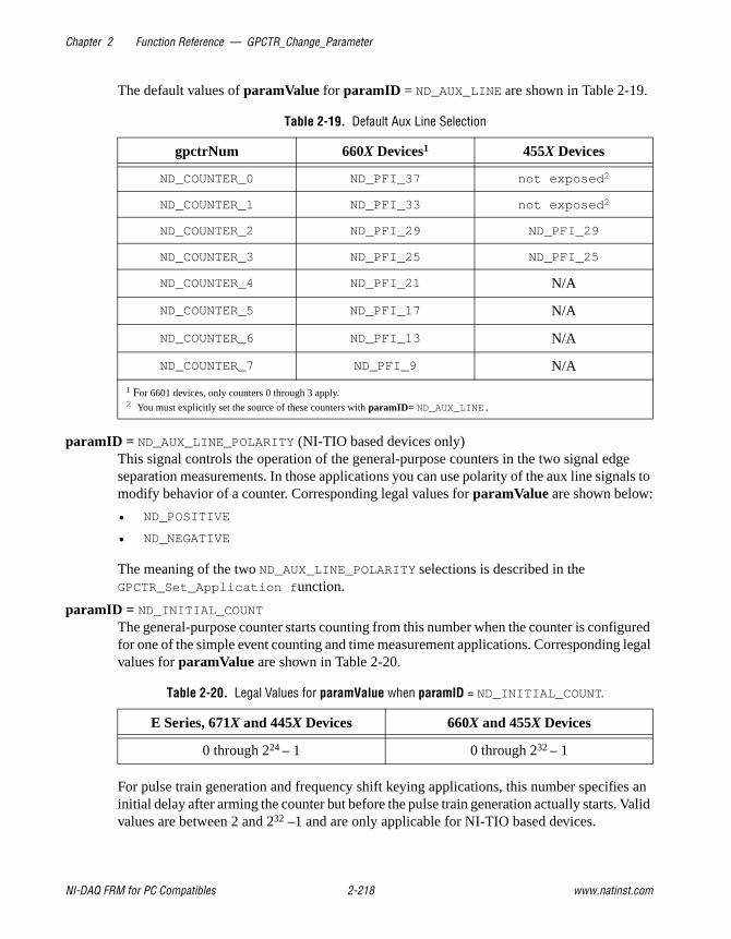
Chapter 2 Function Reference — GPCTR_Change_Parameter
NI-DAQ FRM for PC Compatibles 2-218 www.natinst.com
The default values of paramValue for paramID = ND_AUX_LINE are shown in Table 2-19.
paramID = ND_AUX_LINE_POLARITY (NI-TIO based devices only)This signal controls the operation of the general-purpose counters in the two signal edge separation measurements. In those applications you can use polarity of the aux line signals to modify behavior of a counter. Corresponding legal values for paramValue are shown below:
• ND_POSITIVE
• ND_NEGATIVE
The meaning of the two ND_AUX_LINE_POLARITY selections is described in the GPCTR_Set_Application f unction.
paramID = ND_INITIAL_COUNT
The general-purpose counter starts counting from this number when the counter is configured for one of the simple event counting and time measurement applications. Corresponding legal values for paramValue are shown in Table 2-20.
For pulse train generation and frequency shift keying applications, this number specifies an initial delay after arming the counter but before the pulse train generation actually starts. Valid values are between 2 and 232 –1 and are only applicable for NI-TIO based devices.
Table 2-19. Default Aux Line Selection
gpctrNum 660X Devices1 455X Devices
ND_COUNTER_0 ND_PFI_37 not exposed 2
ND_COUNTER_1 ND_PFI_33 not exposed 2
ND_COUNTER_2 ND_PFI_29 ND_PFI_29
ND_COUNTER_3 ND_PFI_25 ND_PFI_25
ND_COUNTER_4 ND_PFI_21 N/A
ND_COUNTER_5 ND_PFI_17 N/A
ND_COUNTER_6 ND_PFI_13 N/A
ND_COUNTER_7 ND_PFI_9 N/A
1 For 6601 devices, only counters 0 through 3 apply. 2 You must explicitly set the source of these counters with paramID= ND_AUX_LINE.
Table 2-20. Legal Values for paramValue when paramID = ND_INITIAL_COUNT.
E Series, 671X and 445X Devices 660X and 455X Devices
0 through 224 – 1 0 through 232 – 1

Chapter 2 Function Reference — GPCTR_Change_Parameter
© National Instruments Corporation 2-219 NI-DAQ FRM for PC Compatibles
paramID = ND_COUNT_1, ND_COUNT_2, ND_COUNT_3, ND_COUNT_4
The general-purpose counter uses these numbers for pulse width specifications when the counter is configured for one of the simple pulse and pulse train generation applications. Corresponding legal values for paramValue are shown in Table 2-21.
You may seamlessly change the frequency of your pulse train if you call GPCTR_Set_Application with application = ND_PULSE_TRAIN_GNR. To do so, you can call GPCTR_Change_Parameter with paramID = ND_COUNT_1 or ND_COUNT_2 after you have started your pulse train. Then call GPCTR_Control with action = ND_SWITCH_CYCLE to activate the new duty cycle.
paramID = ND_AUTOINCREMENT_COUNT
The value specified by ND_COUNT_1 is incremented by the value selected by ND_AUTOINCREMENT_COUNT every time the counter is reloaded with the value specified by ND_COUNT_1.
For example, with this feature you can generate retriggerable delayed pulses with incrementally increasing delays. You can then use these pulses for applications such as equivalent time sampling (ETS). Corresponding legal values for paramValue are 0 through 28 – 1.
paramID = ND_UP_DOWN
When the application is ND_SIMPLE_EVENT_CNT or ND_BUFFERED_EVENT_CNT, you can use the up or down control options of the counters. Software or hardware can perform the up or down control.
Software ControlThe software up or down control is available by default; if you do not use the GPCTR_Change_Parameter function with paramID set to ND_UP_DOWN, the counter is configured for the software up or down control and starts counting up or down as required by your application. To set the counting direction prior to counting, use the GPCTR_Change_Parameter function with the paramID set to ND_UP_DOWN and the paramValue set to ND_COUNT_DOWN. To change the counting direction while counting is in progress, use the GPCTR_Control function with the action set to ND_COUNT_UP or ND_COUNT_DOWN.
Hardware ControlTo use a hardware signal to control the counting direction, use I/O connector lines as shown in Table 2-22; the counter will count down when the I/O line is in the low state and up when
Table 2-21. Legal Values for paramValue when paramID = ND_COUNT_1, ND_COUNT_2, ND_COUNT_3, and ND_COUNT_4.
E Series, 671X and 445X Devices 660X and 455X Devices
2 through 224 – 1 2 through 232 – 1

Chapter 2 Function Reference — GPCTR_Change_Parameter
NI-DAQ FRM for PC Compatibles 2-220 www.natinst.com
it is in the high state. Use the GPCTR_Change_Parameter function with the paramID set to ND_UP_DOWN and the paramValue set to ND_HARDWARE to take advantage of this counter feature.
.
paramID = ND_BUFFER_MODE Corresponding legal values for paramValue are shown below:
• ND_SINGLE for single buffer operation.
• ND_CONTINUOUS for continuous buffer operation.
paramID = ND_OUTPUT_MODE
This value changes the output mode from default toggle (the output of the counter toggles on each terminal count) to pulsed (the output of the counter makes a pulse on each terminal count). A counter reaches its terminal count each time it reaches zero from either direction. The corresponding settings of paramValue are ND_PULSE and ND_TOGGLE. Also, you might need to enable your output pin with Select_Signal .
paramID = ND_OUTPUT_POLARITY
This paramID allows you to change the output polarity from default positive (the normal state of the output is TTL low) to negative (the normal state of the output is TTL-high). The corresponding settings of paramValue are ND_POSITIVE and ND_NEGATIVE. Also, you might need to enable your output pin with Select_Signal .
paramID = ND_COUNTING_SYNCHRONOUS (for NI-TIO based devices only)This paramID allows the counter to count synchronously or asynchronously. By default, the NI-TIO and STC count asynchronously.
Table 2-22. Default Up/Down Selection
gpctrNumE Series and 671X Devices 660X Devices1 455X Devices
ND_COUNTER_0 Digital I/O Line 6 ND_PFI_37 not exposed 2
ND_COUNTER_1 Digital I/O Line 7 ND_PFI_33 not exposed 2
ND_COUNTER_2 N/A ND_PFI_29 ND_PFI_29
ND_COUNTER_3 N/A ND_PFI_25 ND_PFI_25
ND_COUNTER_4 N/A ND_PFI_21 N/A
ND_COUNTER_5 N/A ND_PFI_17 N/A
ND_COUNTER_6 N/A ND_PFI_13 N/A
ND_COUNTER_7 N/A ND_PFI_9 N/A
1 For 6601 devices, only counters 0 through 3 apply. 2 You cannot use up/down pins with counters 0 and 1.

Chapter 2 Function Reference — GPCTR_Change_Parameter
© National Instruments Corporation 2-221 NI-DAQ FRM for PC Compatibles
Asynchronous counting can cause problems during a buffered acquisition when no source edges are present between two gate edges. A false repetitive reading is made in this case.
To get around this problem, set the NI-TIO into a synchronous counting mode. This always latches the correct value when you encounter no source edges between two gate edges. If you receive source edges at a rate greater than or equal to half of the maximum timebase, then you should not use synchronous mode. Use synchronous mode for buffered acquisitions with a source slower than half the maximum timebase only.
Valid value for paramValue are ND_NO and ND_YES.
Using This FunctionThis function lets you customize the counter for your application. You can use this function after the GPCTR_Set_Application function, and before GPCTR_Control function with action = ND_PREPARE or action = ND_PROGRAM. You can call this function as many times as you need to.

Chapter 2 Function Reference — GPCTR_Config_Buffer
NI-DAQ FRM for PC Compatibles 2-222 www.natinst.com
GPCTR_Config_Buffer
Formatstatus = GPCTR_Config_Buffer (deviceNumber, gpctrNum, reserved, numPoints, buffer)
PurposeAssigns a buffer that NI-DAQ will use for a buffered counter operation.
ParametersInput
Input/Output
Parameter DiscussionThe legal range for gpctrNum is given in terms of constants defined in a header file. The header file you should use depends on the language you are using:
• C programmers—NIDAQCNS.H (DATAACQ.H for LabWindows/CVI)
• BASIC programmers—NIDAQCNS.INC (Visual Basic for Windows programmers should refer to the Programming Language Considerations section in Chapter 1, Using the NI-DAQ Functions, for more information.)
• Pascal programmers—NIDAQCNS.PAS
gpctrNum indicates which counter to program. Legal values for this parameter are in Table 2-13.
numPoints is the number of data points the buffer can hold. The definition of a data point depends on the application the counter is used for. Legal range is 2 through 232 – 1.
Name Type Description
deviceNumber i16 assigned by configuration utility
gpctrNum u32 number of the counter to use
reserved u32 reserved parameter, must be 0
numPoints u32 number of data points the buffer can hold
Name Type Description
buffer [u32] conversion samples returned

Chapter 2 Function Reference — GPCTR_Config_Buffer
© National Instruments Corporation 2-223 NI-DAQ FRM for PC Compatibles
When you use the counter for one of the buffered event counting or buffered time measurement operations, a data point is a single counted number.
buffer is an array of unsigned 32-bit integers.
Using This FunctionYou need to use this function to use a general-purpose counter for buffered operation. You should call this function after calling the GPCTR_Set_Application function.
NI-DAQ transfers counted values into the buffer assigned by this function when you are performing a buffered counter operation.
If you are using the general-purpose counter for
• ND_BUFFERED_EVENT_CNT,
• ND_BUFFERED_PERIOD_MSR,
• ND_BUFFERED_SEMI_PERIOD_MSR,
• ND_BUFFERED_POSITION_MSR,
• ND_BUFFERED_PULSE_WIDTH_MSR, or
• ND_BUFFERED_TWO_SIGNAL_EDGE_SEPARATION_MSR
you should wait for the operation to be completed before accessing the buffer if ND_BUFFER_MODE = ND_SINGLE
If you specify ND_BUFFERED_MODE to be ND_SINGLE, you set up a single buffered operation. For single buffered operations, the operation stops when the buffer has been filled—if you wish to acquire more data, you need to set up the operation again. If you wish to acquire data continuously, you should set ND_BUFFER_MODE to ND_CONTINUOUS. In continuous buffered operation mode you can useGPCTR_Read_Buffer to access parts of the buffer while the operation is in progress.

Chapter 2 Function Reference — GPCTR_Control
NI-DAQ FRM for PC Compatibles 2-224 www.natinst.com
GPCTR_Control
Formatstatus = GPCTR_Control (deviceNumber, gpctrNum, action)
PurposeControls the operation of the general-purpose counter.
ParametersInput
Parameter DiscussionLegal ranges for the gpctrNum and action are given in terms of constants defined in a header file. The header file you should use depends on the language you are using:
• C programmers—NIDAQCNS.H (DATAAQC.H for LabWindows/CVI)
• BASIC programmers—NIDAQCNS.INC (Visual Basic for Windows programmers should refer to the Programming Language Considerations section in Chapter 1, Using the NI-DAQ Functions, for more information.)
• Pascal programmers—NIDAQCNS.PAS
gpctrNum indicates which counter to program. Legal values for this parameter are shown in Table 2-13.
Name Type Description
deviceNumber i16 assigned by configuration utility
gpctrNum u32 number of the counter to use
action u32 the action NI-DAQ takes

Chapter 2 Function Reference — GPCTR_Control
© National Instruments Corporation 2-225 NI-DAQ FRM for PC Compatibles
action is what NI-DAQ performs with the counter. Legal values for this parameter are as follows.
Table 2-23. Legal Values for the action Parameter
action Description
ND_PREPARE Prepare the general-purpose counter for the operation selected by invocations of the GPCTR_Set_Application and (optionally) GPCTR_Change_Parameter function. Do not arm the counter.
ND_ARM Prepares the counter to start, for example, with the gate going high. If the gate has already gone high, the counter starts counting.
ND_DISARM Restores the state of the counter, as if you had not called ND_ARM, regardless of whether the counter is currently counting. This parameter works like an ND_STOP parameter because it stops the counter.
ND_PROGRAM ND_PREPARE and then ND_ARM the counter.
ND_RESET Returns the counter to the power-on state but does not change the polarity.
ND_COUNT_UP Change the counting direction to UP. For gpctrNum = ND_COUNTER_X only. See Using This Function below.
ND_COUNT_DOWN Change the counting direction to DOWN. For gpctrNum = ND_COUNTER_X only. See Using This Function below.
ND_SWITCH_CYCLE This action can be used to change the properties of a continuous pulse that was started using GPCTR_Set_Application with application = ND_PULSE_TRAIN_GNR. If you use ND_SWITCH_CYCLE after the counter is armed, the counter will be reloaded with the latest values specified by GPCTR_Change_Parameter with paramID = ND_COUNT_1 and ND_COUNT_2. For gpctrNum = ND_COUNTER_X only.
ND_SNAPSHOT This action sets several buffer-related readable parameters.

Chapter 2 Function Reference — GPCTR_Control
NI-DAQ FRM for PC Compatibles 2-226 www.natinst.com
Using This FunctionYou should use the following sequence of calls to start your counter:
1. GPCTR_Set_Application
2. GPCTR_Change_Parameter (optional)
3. GPCTR_Config_Buffer (optional)
4. GPCTR_Control (to start the counter)
Typically, you need only one GPCTR_Control call (as shown above) with action= ND_PROGRAM to prepare and arm your computer. If you need to minimize the time between a software event (a call to GPCTR_Control ) and a hardware action (when the counter starts counting), use two calls to GPCTR_Control instead. The first call with action = ND_PREPARE prepares your counter for the application you specify. The second call with action = ND_ARM arms the counter.
You can use this function with action = ND_RESET when you want to halt the operation the general-purpose counter is performing.
Use actions ND_COUNT_UP and ND_COUNT_DOWN to change the counting direction. You can do this only when your application is ND_SIMPLE_EVENT_CNT or ND_BUFFERED_EVENT_CNT and the counter is configured for software control of the counting direction for up or down.
Use action ND_SWITCH_CYCLE only if your application is ND_PULSE_TRAIN_GNR.
Use action ND_SNAPSHOT for capturing real-time information on buffered acquisitions. This action sets the following parameters:
• ND_READ_MARK_H_SNAPSHOT
• ND_READ_MARK_L_SNAPSHOT
• ND_WRITE_MARK_H_SNAPSHOT
• ND_WRITE_MARK_L_SNAPSHOT
• ND_BACKLOG_H_SNAPSHOT
• ND_BACKLOG_L_SNAPSHOT
• ND_ARMED_SNAPSHOT
You can read these values with a GPCTR_Watch call as explained in the GPCTR_Watch
function description.
• ND_SECONDS–for gpctrNum = ND_RTC_X only.
• ND_NANO_SECONDS–for gpctrNum = ND_RTC_X only.

Chapter 2 Function Reference — GPCTR_Read_Buffer
© National Instruments Corporation 2-227 NI-DAQ FRM for PC Compatibles
GPCTR_Read_Buffer
Formatstatus = GPCTR_Read_Buffer (deviceNumber, gpctrNum, readMode, readOffSet,
numPtsToRead, timeOut, numPtsRead,buffer)
PurposeReturns the data from a asynchronous counter input operation. The read mode and offset combined allow you to specify the location from which to read the data.
ParametersInput
Output
Input/Output
Parameter DiscussiongpctrNum indicates which counter to program. Legal values for this parameter are shown in Table 2-13.
Name Type Description
deviceNumber i16 assigned by configuration utility
gpctrNum u32 number of the counter to use
readMode u32 the parameter to set the reading point in the buffer
readOffSet i32 the offset from the reading point
numPtsToRead u32 the number of points to read
timeOut f64 time for which this function will wait before returning
Name Type Description
numPtsRead u32 the number of points actually read
Name Type Description
buffer [u32] conversion samples returned

Chapter 2 Function Reference — GPCTR_Read_Buffer
NI-DAQ FRM for PC Compatibles 2-228 www.natinst.com
The type of read operation specified in readMode is used in conjunction with the readOffSet to compute the reading mark. Basically, read mark = reading point (specified by readMode) + readOffSet. The readMode can have the following legal values:
• ND_READ_MARK—The reading point is placed at the location of the current read mark.
• ND_BUFFER_START—The reading point is placed at the start of the buffer.
• ND_WRITE_MARK—The reading point is placed at a position in the buffer that has the latest data.
readOffSet is the offset that is added to the reading point specified by readMode to compute the location in the buffer from which data is to be read.
numPtsToRead is the number of points to retrieve from the buffer being used.
timeOut is the time in seconds that specifies the maximum amount of time this function should wait before returning. If timeOut is 0, this function returns immediately. If the requested amount of data is not available, the appropriate error code is returned.
status is the return value that specifies success (return value 0) or overWriteError .
numPtsRead is passed by reference. When this function returns, numPtsRead holds the value of the actual number of inputs that were read.
buffer is the destination buffer to hold the retrieved data. Its size should be ≥ numPts.
Using This FunctionYou need to use this function for reading data from a buffer during continuous-buffered or asynchronous data acquisition. Reading the buffer yourself can be dangerous—especially during continuous-buffered operations.
Single buffered operations fill the buffer with data from beginning to end. After the buffer has been filled, the counter disarms itself.
Continuous-buffered operations fill the buffer in a circular manner. If data is not read quickly enough, then it is overwritten. GPCTR_READ_BUFFER takes all this into account when reading the buffer.
This function can report multiple errors. There are three types of errors that this function can report. Here are the rules of precedence:
• Miscellaneous Errors—These types of errors such as invalid errors will typically prevent the function from operating. These types of errors are reported over all other types of errors.

Chapter 2 Function Reference — GPCTR_Read_Buffer
© National Instruments Corporation 2-229 NI-DAQ FRM for PC Compatibles
• overWriteError —This error can be reported during buffered operations. It indicates that the user did not read data from the buffer quickly enough and data was overwritten. If miscellaneous error occurs repeatedly during a read function, this can cause an overWriteError . The miscellaneous errors will be reported over the overWriteError . However, the overWriteError will be reported the next time a miscellaneous error does not occur during a GPCTR_Watch or GPCTR_Read call. Finally, the overWriteError is only issued once per overwrite. If one or more over write errors occur, then one over write error will be issued during the next GPCTR_Watch or GPCTR_Read call.
• dataLossError—This error can be reported during buffered operations. It indicates that the internal counter FIFO overflowed. Once this errors occurs, it is repeatedly reported until the end of the acquisition. All subsequent GPCTR_Watch and GPCTR_Read calls will return this error. Any other error will be reported over a dataLossError.

Chapter 2 Function Reference — GPCTR_Set_Application
NI-DAQ FRM for PC Compatibles 2-230 www.natinst.com
GPCTR_Set_Application
Formatstatus = GPCTR_Set_Application (deviceNumber, gpctrNum, application)
PurposeSelects the application for which you use the general-purpose counter.
ParametersInput
Parameter DiscussionLegal ranges for gpctrNum and application are given in terms of constants that are defined in a header file. The header file you should use depends on which of the following languages you are using:
• C programmers—NIDAQCNS.H (DATAACQ.H for LabWindows/CVI)
• BASIC programmers—NIDAQCNS.INC (Visual Basic for Windows programmers should refer to the Programming Language Considerations section in Chapter 1, Using the NI-DAQ Functions, for more information.)
• Pascal programmers—NIDAQCNS.PAS
gpctrNum indicates which counter to program. Legal values for this parameter are shown in Table 2-13.
Name Type Description
deviceNumber i16 assigned by configuration utility
gpctrNum u32 number of the counter to use
application u32 application for which to use the counter

Chapter 2 Function Reference — GPCTR_Set_Application
© National Instruments Corporation 2-231 NI-DAQ FRM for PC Compatibles
application can be one of the following.
Table 2-24. Descriptions for application
Group Application Description
Simple Counting and Time Measurement
ND_SIMPLE_EVENT_CNT Simple event counting
ND_SINGLE_PERIOD_MSR Simple single period measurement
ND_SINGLE_PULSE_WIDTH_MSR Simple single pulse-width measurement
ND_TRIG_PULSE_WIDTH_MSR Pulse-width measurement you can use for recurring pulses
ND_TWO_SIGNAL_EDGE_SEPARATION_MSRMeasurement between edges of two separate signals (NI-TIO based devices only)
ND_POSITION_MSR Tracks position for motion encoder based applications (NI-TIO based devices only)
Simple Pulse and Pulse Train Generation
ND_SINGLE_PULSE_GNR Generation of a single pulse
ND_SINGLE_TRIG_PULSE_GNR Generation of a single triggered pulse
ND_RETRIG_PULSE_GNR Generation of a retriggerable single pulse
ND_PULSE_TRAIN_GNR Generation of pulse train
ND_FSK Frequency Shift-Keying
Buffered Counting and Time Measurement
ND_BUFFERED_EVENT_CNT Buffered, asynchronous event counting
ND_BUFFERED_PERIOD_MSR Buffered, asynchronous period measurement
ND_BUFFERED_SEMI_PERIOD_MSR Buffered, asynchronous semi-period measurement
ND_BUFFERED_PULSE_WIDTH_MSR Buffered, asynchronous pulse-width measurement
ND_BUFFERED_TWO_SIGNAL_EDGE_
SEPARATION_MSR
Buffered, asynchronous measurement between edges on two separate signals. (NI-TIO based devices only)
ND_BUFFERED_POSITION_MSR Buffered, position tracking of quadrature encoders (NI-TIO based devices only)
_CNT indicates Counting_MSR indicates Measurement_GNR indicates Generation

Chapter 2 Function Reference — GPCTR_Set_Application
NI-DAQ FRM for PC Compatibles 2-232 www.natinst.com
Using This FunctionNI-DAQ requires you to select a set of parameters so that it can program the counter hardware. Those parameters include, for example, signals to be used as counter source and gate and the polarities of those signals. A full list of the parameters is given in the description of the GPCTR_Change_Parameter function. By using the GPCTR_Set_Application function, you assign specific values to all of those parameters. If you want to change the default settings used by this function, you can alter them by using the GPCTR_Change_Parameter function.
When using DMA for buffered GPCTR operations on E Series and 445X devices, you should use the internal 20 MHz timebase over the internal 100 kHz timebase. The 100 kHz timebase does not work correctly when you are using DMA. For measuring gate signals slower than the internal 20 MHz timebase will allow, or when you need to use DMA, we recommend using external timebases. You can use DMA operations on typical 486-based machines without any errors for gate signals of up to 50 kHz using the internal 20 MHz timebase. Trying to achieve rates higher than 50 kHz might cause gpctrDataLossError. This error might cause some computers to lock up because of a memory parity error.
The behavior of the counter you are preparing for an application with this function depends on application, your future calls of the GPCTR functions, and the signals supplied to the counter. The following paragraphs illustrate typical scenarios.
application = ND_SIMPLE_EVENT_CNT
In this application, the counter is used for simple counting of events. By default, the events are low-to-high transitions on the default source pins (see Table 2-16 for default source selections). The counter counts up starting from 0, and it is not gated. You can set the gate by using GPCTR_Change_Parameter . This allows you to gate or control whether the counter is active. The counter is active only when the gate is high.
Figure 2-19 shows one possible scenario of a counter used for ND_SIMPLE_EVENT_CNT after the following programming sequence:
GPCTR_Control(deviceNumber, gpctrNum, ND_RESET)
GPCTR_Set_Application(deviceNumber, gpctrNum, ND_SIMPLE_EVENT_CNT)
GPCTR_Control(deviceNumber, gpctrNum, ND_PROGRAM)
In Figure 2-19, the following behavior is present:
• Source is the signal present at the counter source input.
• Count is the value you would read from the counter if you called the GPCTR_Watch function with entityID = ND_COUNT. The different numbers illustrate behavior at different times

Chapter 2 Function Reference — GPCTR_Set_Application
© National Instruments Corporation 2-233 NI-DAQ FRM for PC Compatibles
Figure 2-19. Simple Event Counting
The following pseudocode continuation of the example given earlier illustrates what you can do to read the counter value continuously (GPCTR_Watch function with entityID = ND_COUNT does this) and print it:
Repeat Forever
GPCTR_Watch(deviceNumber, gpctrNum, ND_COUNT, counterValue)
Output counterValue.
When the counter reaches terminal count (TC), it rolls over and keeps counting. TC is reached when a counter reaches zero from either direction. To check if this occurred, use GPCTR_Watch function with entityID set to ND_TC_REACHED. Refer to Table 2-25 for TC for E Series, 671X, 445X, 455X, and 660X devices.
Typically, you will find modifying the following parameters through the GPCTR_Change_Parameter function useful when the counter application is ND_SIMPLE_EVENT_CNT. You can change the following:
• ND_SOURCE to any value
• ND_SOURCE_POLARITY to ND_HIGH_TO_LOW
• ND_GATE to any legal value listed in the GPCTR_Change_Parameter function description.
• ND_GATE_POLARITY to ND_NEGATIVE to count only when the gate is low.
You can use the GPCTR_Change_Parameter function after calling GPCTR_Set_Application and before calling GPCTR_Control with action = ND_PROGRAM or ND_PREPARE.
Table 2-25. Terminal Count
E Series, 671X and 445X Devices 660X and 455X Devices
224 – 1 232 – 1
0 1 2
Source
Count 5 6 6

Chapter 2 Function Reference — GPCTR_Set_Application
NI-DAQ FRM for PC Compatibles 2-234 www.natinst.com
application = ND_SINGLE_PERIOD_MSR
In this application, the counter is used for a single measurement of the time interval between two transitions of the same polarity of the gate signal. By default, the events are low-to-high transitions on the default gate connector pins (see Table 2-18). The counter uses the 20 MHz internal timebase (ND_INTERNAL_20_MHZ) as its source, so the resolution of measurement is 50 ns. The counter counts up starting from 0.
With the default 20 MHz timebase, combined with the counter width (24 bits), you can measure a time interval between 100 ns and 0.8 s long. For the NI-TIO based devices, the 32 bit wide counters allow you to measure a time interval between 100 ns and 214 s long using this timebase. If you wish to achieve greater resolution, you can use max-timebase (ND_INTERNAL_MAX_TIMEBASE) instead.
Figure 2-20 shows one possible scenario of a counter used for ND_SINGLE_PERIOD_MSR after the following programming sequence:
GPCTR_Control(deviceNumber, gpctrNum, ND_RESET)
GPCTR_Set_Application(deviceNumber, gpctrNum, ND_SINGLE_PERIOD_MSR)
GPCTR_Control(deviceNumber, gpctrNum, ND_PROGRAM)
In Figure 2-20, the following behavior is present:
• Gate is the signal present at the counter gate input.
• Source is the signal present at the counter source input.
• Count is the value you would read from the counter if you called the GPCTR_Watch function with entityID = ND_COUNT. The different numbers illustrate behavior at different times.
• Armed is the value you would read from the counter if you called the GPCTR_Watch function with entityID = ND_ARMED. The different values illustrate behavior at different times.
Figure 2-20. Single Period Measurement
0 1
YES YES
2 3 4 4 4 4
Gate
Source
Count
Armed
MeasuredInterval
NO NO NO

Chapter 2 Function Reference — GPCTR_Set_Application
© National Instruments Corporation 2-235 NI-DAQ FRM for PC Compatibles
Use the GPCTR_Watch function with entityID = ND_ARMED to monitor the progress of the counting process. This measurement completes when entityValue becomes ND_NO. When the counter is no longer armed, you can retrieve the counted value by using GPCTR_Watch with entityID = ND_COUNT. You can do this as follows:
Create u32 variable counter_armed.
Create u32 variable counted_value.
repeat
GPCTR_Watch(deviceNumber, gpctrNumber, ND_ARMED, counter_armed)
until (counter_armed = ND_NO)
GPCTR_Watch(deviceNumber, gpctrNumber, ND_COUNT, counted_value)
To calculate the measured interval, you need to multiply the counted value by the period corresponding to the timebase you are using. For example, if your ND_SOURCE is ND_INTERNAL_20_MHZ, the interval will be 1/(20 MHz) = 50 ns. If the ND_COUNT is 4, (Figure 2-20), the actual interval is 4 * 50 ns = 200 ns.
When the counter reaches terminal count (see Table 2-25), it rolls over and keeps counting. To check if this occurred, use the GPCTR_Watch function with entityID set to ND_TC_REACHED.
Typically, you will find modifying the following parameters through the GPCTR_Change_Parameter function useful when the counter application is ND_SINGLE_PERIOD_MSR. You can change the following:
• ND_SOURCE to ND_INTERNAL_100_KHZ. With this timebase, you can measure the time interval between 20 µs and 160 s for E Series, 671X, and 445X (24 bits) devices and a time interval of 20 µs and 11.37 hours for NI-TIO based devices (32 bits). The resolution will be lower than that you obtain using the ND_INTERNAL_20_MHZ timebase. For NI-TIO based devices, you can use ND_INTERNAL_MAX_TIMEBASE for higher resolution.
• ND_SOURCE_POLARITY to ND_HIGH_TO_LOW.
• ND_GATE to any legal value listed in the GPCTR_Change_Parameter function description.
• ND_GATE_POLARITY to ND_NEGATIVE. The interval will be measured from a high-to-low to the next high-to-low transition of the gate signal.
You can use the GPCTR_Change_Parameter function after calling GPCTR_Set_Application and before calling GPCTR_Control with action = ND_PROGRAM or ND_PREPARE.

Chapter 2 Function Reference — GPCTR_Set_Application
NI-DAQ FRM for PC Compatibles 2-236 www.natinst.com
To provide an external timebase, you can connect your timebase source to an appropriate PFI pin on the I/O connector and change ND_SOURCE and ND_SOURCE_POLARITY to the appropriate values.
You also can configure the other general-purpose counter for ND_PULSE_TRAIN_GNR and set ND_SOURCE of this counter to ND_OTHER_GPCTR_TC to measure intervals longer than the interval timebases allow.
application = ND_SINGLE_PULSE_WIDTH_MSR
In this application, the counter is used for a single measurement of the time interval between two transitions of the opposite polarity of the gate signal. By default, the measurement is performed between a low-to-high and a high-to-low transition on the default I/O connector gate pin (refer to Table 2-18). The counter uses the 20 MHz internal timebase (ND_INTERNAL_20_MHZ) as its source, so the resolution of measurement is 50 ns. The counter counts up starting from zero. For the E Series, 671X and 445X devices with counter width of 24 bits, you can measure a time interval between 100 ns and 0.8 s long. For the NI-TIO based devices, the 32-bit wide counters allow you to measure a time interval between 100 ns and 214 s long using this timebase. If you wish to achieve greater resolution, you may use max-timebase (ND_INTERNAL_MAX_TIMEBASE) instead.
Figure shows one possible scenario of a counter used for ND_SINGLE_PULSE_WIDTH_MSR after the following programming sequence:
GPCTR_Control(deviceNumber, gpctrNum, ND_RESET)
GPCTR_Set_Application(deviceNumber, gpctrNum,
ND_SINGLE_PULSE_WIDTH_MSR)
GPCTR_Control(deviceNumber, gpctrNum, ND_PROGRAM)
In Figure 2-21, the following behavior is present:
• Gate is the signal present at the counter gate input.
• Source is the signal present at the counter source input.
• Count is the value you would read from the counter if you called the GPCTR_Watch function with entityID = ND_COUNT. The different numbers illustrate behavior at different times.
• Armed is the value you read from the counter if you call the GPCTR_Watch function with entityID = ND_ARMED. The different values illustrate behavior at different times.

Chapter 2 Function Reference — GPCTR_Set_Application
© National Instruments Corporation 2-237 NI-DAQ FRM for PC Compatibles
Figure 2-21. Single Pulse Width Measurement
Use the GPCTR_Watch function with entityID = ND_ARMED to monitor the progress of the counting process. This measurement completes when entityValue becomes ND_NO. When the counter is no longer armed, you can retrieve the counted value by using GPCTR_Watch with entityID = ND_COUNT, as shown in the following example code:
Create u32 variable counter_armed.
Create u32 variable counter_value.
Repeat
GPCTR_Watch(deviceNumber, gpctrNumber, ND_ARMED, counter_armed)
until (counter_armed = ND_NO)
GPCTR_Watch(deviceNumber, gpctrNumber, ND_COUNT, counter_value)
To calculate the measured interval, multiply the counted value by the period corresponding to the timebase you are using. For example, if your ND_SOURCE is ND_INTERNAL_20_MHZ, the interval will be 1/(20 MHz) = 50 ns. If the ND_COUNT is 4 (Figure 2-20), the actual interval is 4 * 50 ns = 200 ns.
When the counter reaches TC (Terminal Count), it rolls over and keeps counting. To check if this occurred, use the GPCTR_Watch function with entityID set to ND_TC_REACHED.
Typically, you will find modifying the following parameters through the GPCTR_Change_Parameter function useful when the counter application is ND_SINGLE_PULSE_WIDTH_MSR. You can change the following:
• ND_SOURCE to ND_INTERNAL_100_KHZ. With this timebase, you can measure the time interval between 20 µs and 160 s for E Series, 671X, and 445X (24 bits) devices and a time interval of 20 µs and 11.37 hours for NI-TIO based devices (32 bits). The resolution will be lower than that you obtain using the ND_INTERNAL_20_MHZ timebase. For
0 1
YES YES
2
Gate
Source
Count
Armed
MeasuredInterval
NO NO
2 2 2 22

Chapter 2 Function Reference — GPCTR_Set_Application
NI-DAQ FRM for PC Compatibles 2-238 www.natinst.com
NI-TIO based devices, you can use ND_INTERNAL_MAX_TIMEBASE for higher resolution.
• ND_SOURCE_POLARITY to ND_HIGH_TO_LOW.
• ND_GATE to any legal value listed in the GPCTR_Change_Parameter function description.
• ND_GATE_POLARITY to ND_NEGATIVE. The pulse width will be measured from a high-to-low to the next low-to-high transition of the gate signal.
You can use the GPCTR_Change_Parameter function after calling GPCTR_Set_Application and before calling GPCTR_Control with action = ND_PROGRAM or ND_PREPARE.
To provide an external timebase, connect your timebase source to an appropriate PFI pin on the I/O connector and change ND_SOURCE and ND_SOURCE_POLARITY to the appropriate values.
You can also configure the other general-purpose counter for ND_PULSE_TRAIN_GNR and set ND_SOURCE of this counter to ND_OTHER_GPCTR_TC to measure pulse widths longer than 160 s for E Series, 671X, and 445X devices and 11.37 hours for NI-TIO devices.
Caution For DAQ-STC based devices, application ND_SINGLE_PULSE_WIDTH
measurements function correctly only if the gate is in the inactive state when the counter is armed by GPCTR_Control . If the gate is in the active state when the counter is armed via GPCTR_Control , you will see a gateSignalError returned. If this happens, you should not rely on values returned by GPCTR_Watch.
application = ND_TRIG_PULSE_WIDTH_MSR
In this application, the counter is used for a single measurement of the time interval between two transitions of the opposite polarity of the gate signal. By default, the measurement is performed between a low-to-high and a high-to-low transition on the I/O connector default gate pins (see Table 2-18 for default gate pin selection). The counter counts the 20 MHz internal timebase (INTERNAL_20_MHZ), so the resolution of measurement is 50 ns. The counter counts up starting from zero.
Unlike ND_SINGLE_PULSE_WIDTH_MSR, your gate signal can change state during counter arming. However, you need at least two pulses. Assuming positive gate polarity, the high-to-low transition on the first pulse acts as a trigger and allows the counter to begin the measurement on the next low-to-high transition.
The default 20 MHz timebase, combined with the counter width (24 bits), lets you measure the duration of a pulse between 100 ns and 0.8 s long. For the NI-TIO based devices with counter width 32 bits, you can measure pulse duration between 100 ns and 214 s long.

Chapter 2 Function Reference — GPCTR_Set_Application
© National Instruments Corporation 2-239 NI-DAQ FRM for PC Compatibles
Figure 2-22 shows one possible scenario of a counter used for ND_TRIG_PULSE_WIDTH_MSR after the following programming sequence:
GPCTR_Control(deviceNumber, gpctrNum, ND_RESET)
GPCTR_Set_Application(deviceNumber, gpctrNum,
ND_TRIG_PULSE_WIDTH_MSR)
GPCTR_Control(deviceNumber, gpctrNum, ND_PROGRAM)
In Figure 2-22, the following behavior is present:
• Gate is the signal present at the counter gate input.
• Source is the signal present at the counter source input.
• Count is the value you would read from the counter if you called the GPCTR_Watch function with entityID = ND_COUNT. The different numbers illustrate behavior at different times.
• Armed is the value you read from the counter if you call the GPCTR_Watch function with entityID = ND_ARMED. The different values illustrate behavior at different times.
Figure 2-22. Single Triggered Pulse Width Generation Measurement
Use the GPCTR_Watch function with entityID = ND_ARMED to monitor the progress of the counting process. This measurement completes when entityValue becomes ND_NO. After this is completed, you can retrieve the counted value by using GPCTR_Watch with entityID = ND_COUNT, as shown in the following example code:
Create u32 variable counter_armed.
Create u32 variable counter_value.
Repeat
GPCTR_Watch(deviceNumber, gpctrNumber, ND_ARMED, counter_armed)
0 0
YES YES
0
Gate
Source
Count
Armed
MeasuredInterval
YES NO
0 0 1 22
Trigger

Chapter 2 Function Reference — GPCTR_Set_Application
NI-DAQ FRM for PC Compatibles 2-240 www.natinst.com
until (counter_armed = ND_NO)
GPCTR_Watch(deviceNumber, gpctrNumber, ND_COUNT, counter_value)
To calculate the measured interval, multiply the counted value by the period corresponding to the timebase you are using. For example, if your ND_SOURCE is ND_INTERNAL_20_MHZ, the interval will be 1/(20 MHz) = 50 ns. If the ND_COUNT is 4 (Figure 2-20), the actual interval is 4 * 50 ns = 200 ns.
Note The measured interval will correspond to the most recent pulse that arrived prior to the invoking of GPCTR_Watch call with entityID set to ND_COUNT_AVAILABLE.
Caution There should be source transitions between gate transitions in order for this measurement to be correct. NI-TIO based devices can get around this limitation by setting the counter to count synchronously.
When the counter reaches terminal count (224 – 1 for E Series, 671X, and 445X devices, and 232 – 1 for NI-TIO based devices), it rolls over and keeps counting. To check if this occurred, use GPCTR_Watch function with entityID set to ND_TC_REACHED.
Typically, you will find modifying the following parameters through the GPCTR_Change_Parameter function useful when the counter application is ND_TRIG_PULSE_WIDTH_MSR. You can change the following:
• ND_SOURCE to ND_INTERNAL_100_KHZ. With this timebase, you can measure pulse widths between 20 µs and 160 s for E Series, 671X, and 445X devices and pulse widths between 20 µs and 11.37 hours for NI-TIO based devices. The timing resolution will be lower than if you are using the ND_INTERNAL_20_MHZ timebase. For NI-TIO based devices, you can use ND_INTERNAL_MAX_TIMBASE for more timing resolution.
• ND_SOURCE_POLARITY to ND_HIGH_TO_LOW.
• ND_GATE to any legal value listed in the GPCTR_Change_Parameter function description.
• ND_GATE_POLARITY to ND_NEGATIVE. The pulse width will be measured from a high-to-low to the next low-to-high transition of the gate signal. The trigger will occur on a low-to-high transition on the gate signal.
You can use the GPCTR_Change_Parameter function after calling GPCTR_Set_Application and before calling GPCTR_Control with action = ND_PROGRAM or ND_PREPARE.
To provide an external timebase, connect your timebase source to an appropriate PFI pin on the I/O connector and change ND_SOURCE and ND_SOURCE_POLARITY to the appropriate values.

Chapter 2 Function Reference — GPCTR_Set_Application
© National Instruments Corporation 2-241 NI-DAQ FRM for PC Compatibles
You can also configure the other general-purpose counter for ND_PULSE_TRAIN_GNR and set ND_SOURCE of this counter to ND_OTHER_GPCTR_TC to generate pulses with delays and measure interval pulse widths longer than 160 s for E Series and 445X devices. You can generate pulse widths longer than 11.37 hours for NI-TIO based devices by using this application.
application = ND_TWO_SIGNAL_EDGE_SEPARATION_MSR (For NI-TIO based devices only)In this application, the counter is used for a single measurement of the time interval between transitions of the aux line and the gate signal. Measurement starts when the aux line signal is asserted and stops when the gate is asserted. By default, the measurement is performed between a low-to-high transition on the aux line signal and the next low-to-high transition on the gate signal. The default values for aux line and gate signals for the eight counters are shown in Tables 2-19 and 2-18 respectively. The counter uses the 20 MHz internal timebase (ND_INTERNAL_20_MHZ) as its source, so the resolution of measurement is 50 ns. The counter counts up starting from 0.
Using the default 20 MHz timebase, combined with the counter width (32 bits), you can measure the duration of a pulse between 100 ns and 214 s long. You can also set the source to ND_INTERNAL_MAX_TIMEBASE for higher temperature resolution or ND_INTERNAL_100_KHZ for longer measuring times.
Figure 2-23 shows one possible use of a counter for ND_TWO_SIGNAL_EDGE_SEPARATION_MSR after the following programming sequence:
GPCTR_Control (deviceNumber, gpctrNum, ND_RESET)
GPCTR_Set_Application (deviceNumber, gpctrNum,
ND_TWO_SIGNAL_EDGE_SEPARATION_MSR)
GPCTR_Control (deviceNumber, gpctrNum, ND_PROGRAM)
In Figure 2-23, the following behavior is present:
• Aux line is the signal present at the counter aux line input.
• Gate is the signal present at the counter gate input.
• Source is the signal present at the counter source input.
• Count is the value you would read from the counter if you called the GPCTR_Watch function entityID = ND_COUNT. The different numbers illustrate the behavior at different times.
• Armed is the value you would read from the counter if you called the GPCTR_Watch function with entityID = ND_ARMED. The different values illustrate behavior at different times.

Chapter 2 Function Reference — GPCTR_Set_Application
NI-DAQ FRM for PC Compatibles 2-242 www.natinst.com
Figure 2-23. Two Signal Edge Separation Measurement
After the counter is armed, the first active edge on aux line begins the measurement. The measurement ends on the first active edge on gate that occurs after this time. Additional active edges on aux line are ignored, as indicated by Figure 2-23.
Use the GPCTR_Watch function with entityID = ND_ARMED to monitor the progress of the counting process. This measurement completes when entityValue becomes ND_NO. When the counter is no longer armed, you can retrieve the counted value by using GPCTR_Watch with entityID = ND_COUNT, as shown in the following example code:
Create U32 variable counter_armed.
Create U32 variable counter_value.
repeat
GPCTR_Watch (deviceNumber, gpctrNumber, ND_ARMED, counter_armed)
until (counter_armed = ND_NO)
GPCTR_Watch (deviceNumber, gpctrNumber, ND_COUNT, counted_value)
To calculate the measured interval, multiply the counted value by the period corresponding to the timebase you are using. For example, if your ND_SOURCE is ND_INTERVAL_20_MHZ, the interval will be (1/20 MHz) = 50 ns. If the ND_COUNT is 3 (Figure 2-18), the actual interval is 3 * 50 ns = 150 ns.
When the counter reaches terminal count (232 – 1 for NI-TIO based devices), it rolls over and keeps counting. To check if this occurred, use GPCTR_Watch function with entityID set to ND_TC_REACHED.
Source
Count
Armed
3
Gate
Aux Line
10
YES YES YES
2 3 33 3 3 3 33 3
NO NONO NO NO NONO NO

Chapter 2 Function Reference — GPCTR_Set_Application
© National Instruments Corporation 2-243 NI-DAQ FRM for PC Compatibles
Typically, modifying the following parameters through the GPCTR_Change_Parameter function is useful if the counter application is ND_TWO_SIGNAL_EDGE_SEPARATION_MSR. You can change the following:
• ND_SOURCE to ND_INTERNAL_100_KHZ. With this timebase, you can measure intervals between 20 µs and 11.37 hours long. The resolution will be lower than that you will obtain by using ND_INTERVAL_20_MHZ. For NI-TIO based devices, you can use ND_INTERNAL_MAX_TIMEBASE for more timing resolution.
• ND_SOURCE_POLARITY to ND_HIGH_TO_LOW.
• ND_AUX_LINE to any legal value listed in the GPCTR_Change_Parameter function description.
• ND_AUX_LINE_POLARITY to ND_NEGATIVE. Measurement will start on a falling edge.
• ND_GATE to any legal value listed in the GPCTR_Change_Parameter function description.
• ND_GATE_POLARITY to ND_NEGATIVE. Measurement will stop on a falling edge.
To provide an external timebase, connect your timebase source to an appropriate PFI pin on the I/O connector and change ND_SOURCE and ND_SOURCE_POLARITY to the appropriate values.
You can also configure the other general-purpose counter for ND_PULSE_TRAIN_GNR and set ND_SOURCE of this counter to ND_OTHER_GPCTR_TC to generate pulses with delays and measure interval pulse widths longer than 160 s for E Series and 445X devices. You can generate pulse widths longer than 11.37 hours for NI-TIO based devices by using this application.
application = ND_POSITION_MSR (For NI-TIO based devices only)In this application, the counter is used to track the position of a motion encoder. This application works with two types of encoders: quadrature encoders (X1, X2, and X4), and two-pulse encoders (also referred to as up/down encoders).
Encoders generally have three channels: channels A, B, and Z. Two-pulse encoders do not use the Z channel. The A channel is hardwired to the default counter source pin. The B channel is hardwired to the aux line pin. Finally, the Z channel is hardwired to the gate pin. The selected source for the counter determines the timebase of the counter during the position measurement.
The selected source of the counter is set at the maximum internal timebase for the best resolution.
Some quadrature encoders have a third channel: channel Z. Channel Z is also referred to as the index channel. A high level on channel Z causes the counter to be reloaded with a specified value in the phase when A and B are low. You must ensure that channel Z is high during at least a portion of the phase when channel A and B are low. Otherwise, the

Chapter 2 Function Reference — GPCTR_Set_Application
NI-DAQ FRM for PC Compatibles 2-244 www.natinst.com
GPCTR_Change_Parameter with paramID = ND_Z_INDEX_ACTIVE and paramValue = ND_YES. To set the reload value call GPCTR_Change_Parameter with paramID = ND_Z_INDEX_VALUE and paramValue = desired reload value.
Figure 2-24 shows an example of X4 decoding. The reload of the counter occurs when all three channels are high. Also, the actual reload occurs within one max-timebase period after the reload phase becomes true. After the reload occurs, the counter continues to count from the specified reload value.
Figure 2-24. X4 Decoding Example with Z indexing
Typically, you will find modifying the following parameters through the GPCTR_Change_Parameter function useful when the counter application is ND_POSITION_MSR. You can change the following:
• ND_Z_INDEX_ACTIVE to ND_YES to active the Z channel.
• ND_Z_INDEX_VALUE to the desired value for Z indexing.
• ND_INITIAL_COUNT to the desired initial value of the counter.
Note For 455X devices, this application cannot be used with counters 0 and 1.
application = ND_SINGLE_PULSE_GNR
In this application, the counter is used for the generation of single delayed pulse. By default, you use the 20 MHz internal timebase (ND_INTERNAL_20_MHZ), so the resolution of timing is 50 ns. The counter loads ND_COUNT_1 and counts down to zero for the delay time. It then loads ND_COUNT_2 and counts down to zero to generate the pulse. The default values for ND_COUNT_1 and ND_COUNT_2 are 5 million and 10 million, respectively, which give a 0.5 s pulse after a 0.25 s delay.
Using the default 20 MHz timebase, combined with the counter width of 24 bits (E Series and 445X only), you can generate pulses with a delay and length between 100 ns and 0.8 s long. For the NI-TIO based devices, the 32-bit wide counters allow you to measure a time interval between 100 ns and 214 s long using this timebase. If you wish to achieve greater resolution, you may use max-timebase (ND_INTERNAL_MAX_TIMEBASE) instead.
5 6 87A=1B=1Z=1
2109 3 4
Ch A
Ch B
Ch ZMax Time Base
Counter Value

Chapter 2 Function Reference — GPCTR_Set_Application
© National Instruments Corporation 2-245 NI-DAQ FRM for PC Compatibles
For example, assume that you want to generate a pulse 200 ns long after 150 ns of delay. You need to set ND_COUNT_1 to 150 ns/50 ns = 3 and ND_COUNT_2 to 200 ns/50 ns = 4. Figure 2-25 shows the scenario of a counter used for ND_SINGLE_PULSE_GNR after the following programming sequence:
GPCTR_Control(deviceNumber, gpctrNum, ND_RESET)
GPCTR_Set_Application(deviceNumber, gpctrNum, ND_SINGLE_PULSE_GNR)
GPCTR_Change_Parameter(deviceNumber, gpctrNum, ND_COUNT_1, 3)
GPCTR_Change_Parameter(deviceNumber, gpctrNum, ND_COUNT_2, 4)
Select_Signal(deviceNumber, gpctrNumOut, gpctrNumOut,ND_LOW_TO_HIGH)
GPCTR_Control(deviceNumber, gpctrNum, ND_PROGRAM)
In Figure 2-25, the following behavior is present:
• Source is the signal present at the counter source input.
• Output is the signal present at the counter output.
• Armed is the value you would read from the counter if you called the GPCTR_Watch function with entityID = ND_ARMED. The different values illustrate behavior at different times.
Figure 2-25. Single Pulse Generation
Use the GPCTR_Watch function with entityID = ND_ARMED to monitor the progress of the pulse generation process. The generation completes when entityValue becomes ND_NO.
Typically, you find modifying of the following parameters through the GPCTR_Change_Parameter function useful when the counter application is ND_SINGLE_PULSE_GNR. You can change the following:
• ND_COUNT_1 and ND_COUNT_2 to any value between 2 and 224 – 1 for E Series, 671X, and 445X devices, and to any value between 232 – 1 for NI-TIO based devices. The defaults are given for illustrative purposes only.
• ND_SOURCE to ND_INTERNAL_100_KHZ. With this timebase, you can generate pulses with a delay and length between 20 µs and 160 s for E Series, 671X, and 445X devices
Source
Armed No
Output
No
Count_1 = 3 Count_2 = 4
Yes

Chapter 2 Function Reference — GPCTR_Set_Application
NI-DAQ FRM for PC Compatibles 2-246 www.natinst.com
and between 20 ns and 11.37 hours for NI-TIO based devices. The resolution will be lower than that you obtain using the ND_INTERNAL_20_MHZ timebase. For NI-TIO based devices, you can use ND_INTERNAL_MAX_TIMEBASE for higher resolution.
You can use the GPCTR_Change_Parameter function after calling GPCTR_Set_Application and before calling GPCTR_Control with action = ND_PROGRAM or ND_PREPARE.
To provide an external timebase, you can connect your timebase source to an appropriate PFI pin on the I/O connector and change ND_SOURCE and ND_SOURCE_POLARITY to the appropriate values.
You also can configure the other general-purpose counter for ND_PULSE_TRAIN_GNR and set ND_SOURCE of this counter to ND_OTHER_GPCTR_TC to generate pulses with delays and intervals longer than 160 s for E Series, 671X, and 445X devices and 11.37 hours for NI-TIO based devices.
application = ND_SINGLE_TRIG_PULSE_GNR
In this application, the counter is used for the generation of a single delayed pulse after a transition on the gate input. By default, the delayed pulse is generated by using the 20 MHz internal timebase (ND_INTERNAL_20_MHZ), so the resolution of timing is 50 ns. The counter loads ND_COUNT_1 and counts down to zero for the delay time. It then loads ND_COUNT_2 and counts down to zero to generate the pulse. The default values for ND_COUNT_1 and ND_COUNT_2 are 5 million and 10 million, respectively, which give a 0.5 s pulse after a 0.25 s delay. With default settings, a low-to-high transition on the gate signal triggers the pulse generation. The default gate signal is shown in Table 2-18. Only the first transition of the gate signal after you arm the counter triggers pulse generation; all subsequent transitions are ignored.
Using the default 20 MHz timebase, combined with the counter width (24 bits), you can measure a time interval between 100 ns and 0.8 s long for E Series, 671X, and 445X devices only. For the NI-TIO based devices, the 32-bit wide counters allow you to measure a time interval between 100 ns and 214 s long using this timebase. If you wish to achieve greater resolution, you may use max-timebase (ND_INTERNAL_MAX_TIMEBASE) instead.
For example, assume that you want to generate a pulse 200 ns long after 150 ns of delay from the transition of the gate signal. You need to set ND_COUNT_1 to 150 ns/50 ns = 3 and ND_COUNT_2 to 200 ns/50 ns = 4. Figure 2-26 shows the scenario of a counter used for ND_SINGLE_TRIG_PULSE_GNR after the following programming sequence:
GPCTR_Control(deviceNumber, gpctrNum, ND_RESET)
GPCTR_Set_Application(deviceNumber, gpctrNum,
ND_SINGLE_TRIG_PULSE_GNR)
GPCTR_Change_Parameter(deviceNumber, gpctrNum, ND_COUNT_1, 3)
GPCTR_Change_Parameter(deviceNumber, gpctrNum, ND_COUNT_2, 4)

Chapter 2 Function Reference — GPCTR_Set_Application
© National Instruments Corporation 2-247 NI-DAQ FRM for PC Compatibles
Select_Signal(deviceNumber, gpctrNumOut, gpctrNumOut, ND_LOW_TO_HIGH)
GPCTR_Control(deviceNumber, gpctrNum, ND_PROGRAM)
In Figure 2-26, the following behavior is present:
• Gate is the signal present at the counter gate input.
• Source is the signal present at the counter source input.
• Output is the signal present at the counter output.
• Armed is the value you would read from the counter if you called the GPCTR_Watch function with entityID = ND_ARMED. The different values illustrate behavior at different times.
Figure 2-26. Single Triggered Pulse Generation
Use the GPCTR_Watch function with entityID = ND_ARMED to monitor the progress of the pulse generation process. The generation completes when entityValue becomes ND_NO.
Typically, you will find modification of the following parameters through the GPCTR_Change_Parameter function useful when the counter application is ND_SINGLE_TRIG_PULSE_GNR. You can change the following:
• ND_COUNT_1 and ND_COUNT_2 to any value between 2 and 224 – 1 for E Series, 671X, and 445X devices, and to any value between 232 – 1 for NI-TIO based devices. The defaults are given for illustrative purposes only.
• ND_SOURCE to ND_INTERNAL_100_KHZ. With this timebase, you can generate pulses with a delay and length between 20 µs and 160 s. The resolution will be lower than that you obtain by using ND_INTERVAL_20_MHZ. For NI-TIO based devices, you can use ND_INTERNAL_MAX_TIMEBASE for more timing resolution.
• ND_GATE to any legal value listed in the GPCTR_Change_Parameter function description.
• ND_GATE_POLARITY to ND_NEGATIVE. A high-to-low transition of the gate signal triggers the pulse generation timing.
Source
Armed No
Output
No
Count_1 = 3 Count_2 = 4
Yes
Gate

Chapter 2 Function Reference — GPCTR_Set_Application
NI-DAQ FRM for PC Compatibles 2-248 www.natinst.com
You can use the GPCTR_Change_Parameter function after calling GPCTR_Set_Application and before calling GPCTR_Control with action = ND_PROGRAM or ND_PREPARE.
To provide an external timebase, you can connect your timebase source to an appropriate PFI pin on the I/O connector and change ND_SOURCE and ND_SOURCE_POLARITY to the appropriate values.
You also can configure the other general-purpose counter for ND_SINGLE_TRIG_PULSE_GNR and set ND_SOURCE of this counter to ND_OTHER_GPCTR_TC to generate pulses with delays and intervals longer than 160 s.
application = ND_RETRIG_PULSE_GNR
In this application, the counter is used for the generation of a retriggerable delayed pulse after each transition on the gate input. You get this by using the default 20 MHz internal timebase (ND_INTERNAL_20_MHZ), so the timing resolution is 50 ns. The counter loads ND_COUNT_1 and counts down to zero for the delay time. It then loads ND_COUNT_2 and counts down to zero to generate the pulse. The default values for ND_COUNT_1 and ND_COUNT_2 are 5 million and 10 million, respectively, which give a 0.5 s pulse after a 0.25 s delay. With default settings, a low-to-high transition on the gate signal triggers the pulse generation. The default gate signal is shown in Table 2-18. Any gate transitions received during the pulse generation are ignored.
Using the default 20 MHz timebase, combined with the counter width (24 bits), you can measure a time interval between 100 ns and 0.8 s long. For the NI-TIO based devices, the 32-bit wide counters allow you to measure a time interval between 100 ns and 214 s long using this timebase. If you wish to achieve greater resolution, you may use max-timebase (ND_INTERNAL_MAX_TIMEBASE) instead.
For example, assume that you want to generate a pulse 200 ns long after 150 ns of delay from every transition of the gate signal. You need to set ND_COUNT_1 to 150 ns/50 ns = 3 and ND_COUNT_2 to 200 ns/50 ns = 4. Figure 2-27 shows the scenario of a counter used for ND_RETRIG_PULSE_GNR after the following programming sequence:
GPCTR_Control(deviceNumber, gpctrNum, ND_RESET)
GPCTR_Set_Application(deviceNumber, gpctrNum, ND_RETRIG_PULSE_GNR)
GPCTR_Change_Parameter(deviceNumber, gpctrNum, ND_COUNT_1, 3)
GPCTR_Change_Parameter(deviceNumber, gpctrNum, ND_COUNT_2, 4)
Select_Signal(deviceNumber, gpctrNumOut, gpctrNumOut, ND_LOW_TO_HIGH)
GPCTR_Control(deviceNumber, gpctrNum, ND_PROGRAM)
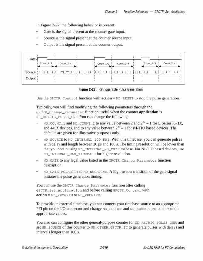
Chapter 2 Function Reference — GPCTR_Set_Application
© National Instruments Corporation 2-249 NI-DAQ FRM for PC Compatibles
In Figure 2-27, the following behavior is present:
• Gate is the signal present at the counter gate input.
• Source is the signal present at the counter source input.
• Output is the signal present at the counter output.
Figure 2-27. Retriggerable Pulse Generation
Use the GPCTR_Control function with action = ND_RESET to stop the pulse generation.
Typically, you will find modifying the following parameters through the GPCTR_Change_Parameter function useful when the counter application is ND_RETRIG_PULSE_GNR. You can change the following:
• ND_COUNT_1 and ND_COUNT_2 to any value between 2 and 224 – 1 for E Series, 671X, and 445X devices, and to any value between 232 – 1 for NI-TIO based devices. The defaults are given for illustrative purposes only.
• ND_SOURCE to ND_INTERNAL_100_KHZ. With this timebase, you can generate pulses with delay and length between 20 µs and 160 s. The timing resolution will be lower than that you obtain using ND_INTERNAL_20_MHZ timebase. For NI-TIO based devices, use ND_INTERNAL_MAX_TIMEBASE for higher resolution.
• ND_GATE to any legal value listed in the GPCTR_Change_Parameter function description.
• ND_GATE_POLARITY to ND_NEGATIVE. A high-to-low transition of the gate signal initiates the pulse generation timing.
You can use the GPCTR_Change_Parameter function after calling GPCTR_Set_Application and before calling GPCTR_Control with action = ND_PROGRAM or ND_PREPARE.
To provide an external timebase, you can connect your timebase source to an appropriate PFI pin on the I/O connector and change ND_SOURCE and ND_SOURCE_POLARITY to the appropriate values.
You also can configure the other general-purpose counter for ND_RETRIG_PULSE_GNR, and set ND_SOURCE of this counter to ND_OTHER_GPCTR_TC to generate pulses with delays and intervals longer than 160 s.
Source
Gate
Output
Count_1=3 Count_2=4 Count_1=3 Count_2=4 Count_1=3 Count_2=4

Chapter 2 Function Reference — GPCTR_Set_Application
NI-DAQ FRM for PC Compatibles 2-250 www.natinst.com
application = ND_PULSE_TRAIN_GNR
In this application, the counter is used for generation of a pulse train. By default, you get this by using the 20 MHz internal timebase (ND_INTERNAL_20_MHZ), so the resolution of timing is 50 ns. The counter loads ND_COUNT_1 and counts down to zero for the delay time. It then loads ND_COUNT_2 and counts down to zero to generate the pulse. The default values for ND_COUNT_1 and ND_COUNT_2 are 5 million and 10 million, respectively, which give a 0.5 s pulse after a 0.25 s delay. The frequency of your pulse train is: frequency = 1/timebase period*(ND_COUNT_1 + ND_COUNT_2). The duty cycle of your pulse train is: duty cycle = ND_COUNT_2/(ND_COUNT_1 + ND_COUNT_2). Pulse train generation starts as soon as you arm the counter. You must reset the counter to stop the pulse train.
Using the default 20 MHz timebase, combined with the counter width (24 bits), you can generate trains consisting of pulses with delay and length between 100 ns and 0.8 s. For NI-TIO based devices, you can generate pulses with a delay and length between 100 ns and 214 s long.
Assume that you want to generate a pulse train with the low period 150 ns long and the high period 200 ns long. You need to set ND_COUNT_1 to 150 ns/50 ns = 3, and ND_COUNT_2 to 200 ns/50 ns = 4.
Figure 2-28 shows the scenario of a counter used for ND_PULSE_TRAIN_GNR after the following programming sequence:
GPCTR_Control(deviceNumber, gpctrNum, ND_RESET)
GPCTR_Set_Application(deviceNumber, gpctrNum, ND_PULSE_TRAIN_GNR)
GPCTR_Change_Parameter(deviceNumber, gpctrNum, ND_COUNT_1, 3)
GPCTR_Change_Parameter(deviceNumber, gpctrNum, ND_COUNT_2, 4)
Select_Signal(deviceNumber, gpctrNumOut, gpctrNumOut, ND_LOW_TO_HIGH)
GPCTR_Control(deviceNumber, gpctrNum, ND_PROGRAM)
In Figure 2-28, the following behavior is present:
• Source is the signal present at the counter source input.
• Output is the signal present at the counter output.
Figure 2-28. Pulse Train Generation
Source
Count_1 = 3 Count_2 = 4 Count_1 = 3 Count_2 = 4
Output

Chapter 2 Function Reference — GPCTR_Set_Application
© National Instruments Corporation 2-251 NI-DAQ FRM for PC Compatibles
Use the GPCTR_Control function with action = ND_RESET to stop the pulse generation.
Typically, you will find modifying the following parameters through the GPCTR_Change_Parameter function useful when the counter application is ND_PULSE_TRAIN_GNR. You can change the following:
• ND_COUNT_1 and ND_COUNT_2 to any value between 2 and 224 – 1 for E Series, 671X, and 445X devices, and to any value between 2 and 232 – 1 for NI-TIO based devices. The defaults are given for illustrative purposes only.
• ND_SOURCE to ND_INTERNAL_100_KHZ. With this timebase, you can generate pulses with delay and length between 20 µs and 160 s. The timing resolution will be lower than that you obtain using the ND_INTERNAL_20_MHZ timebase. For NI-TIO based devices, use ND_INTERNAL_MAX_TIMEBASE for higher resolution.
• ND_INITIAL_COUNT to any value between 2 and 232 –1 to specify an initial delay after arming the counter but before the pulse train generation actually starts. This is only applicable for NI-TIO based devices.
You can use the GPCTR_Change_Parameter function after calling GPCTR_Set_Application and before calling GPCTR_Control with action = ND_PROGRAM or ND_PREPARE.
To provide an external timebase, you can connect your timebase source to an appropriate PFI pin on the I/O connector and change ND_SOURCE and ND_SOURCE_POLARITY to the appropriate values.
You also can configure the other general-purpose counter for ND_PULSE_TRAIN_GNR, and set ND_SOURCE of this counter to ND_OTHER_GPCTR_TC to generate pulses with delays and intervals longer than 160 s.
application = ND_FSK
In this application, the counter is used for generation of frequency shift keyed signals. The counter generates a pulse train of one frequency and duty cycle when the gate is low, and a pulse train with a second set of parameters when the gate is high. By default, you get this by using the 20 MHz internal timebase (ND_INTERNAL_20_MHZ) so the timing resolution is 50 ns. While the gate is low, the counter loads ND_COUNT_1 and count down to zero for the inactive pulse train. It then loads ND_COUNT_2 and counts down for the active phase of the pulse train. The counter repeats in this manner. The FSK pulse generation starts as soon as you arm the counter. You must reset the counter to stop the pulse generation.
While the gate is high, he counter loads ND_COUNT_3 and count down to zero for the inactive pulse train. It then loads ND_COUNT_4 and counts down for the active phase of the pulse train. When the gate changes state, the cycle in progress finishes before the second set of parameters are used.

Chapter 2 Function Reference — GPCTR_Set_Application
NI-DAQ FRM for PC Compatibles 2-252 www.natinst.com
Using the default 20 MHz timebase, combined with the counter width (24 bits), you can generate trains consisting of pulses with delay and length between 100 ns and 0.8 s. For NI-TIO based devices, you can generate pulses with a delay and length between 100 ns and 214 s long.
Assume that you want to generate a pulse train with 100 ns low time and 150 ns high time when the gate is low and with 300 ns low time and 200 ns high time when the gate is high. You need to set ND_COUNT_1 to 100 ns/50 ns = 2, ND_COUNT_2 to 150 ns/50 ns = 3, ND_COUNT_3 to 300 ns/50 ns = 6, and ND_COUNT_4 to 200 ns/50 ns = 4. Figure 2-29 shows a counter used for ND_FSK after the following programming sequence:
GPCTR_Control(deviceNumber, gpctrNum, ND_RESET)
GPCTR_Set_Application(deviceNumber, gpctrNum, ND_FSK)
GPCTR_Change_Parameter(deviceNumber, gpctrNum, ND_COUNT_1, 2)
GPCTR_Change_Parameter(deviceNumber, gpctrNum, ND_COUNT_2, 3)
GPCTR_Change_Parameter(deviceNumber, gpctrNum, ND_COUNT_3, 6)
GPCTR_Change_Parameter(deviceNumber, gpctrNum, ND_COUNT_4, 4)
Select_Signal(deviceNumber, gpctrNumOut, gpctrNumOut, ND_LOW_TO_HIGH)
GPCTR_Control(deviceNumber, gpctrNum, ND_PROGRAM)
In Figure 2-29, the following behavior is present:
• Gate is the signal present at the counter gate input.
• Source is the signal present at the counter source input.
• Output is the signal present at the counter output.
Figure 2-29. Frequency Shift Keying
Use the GPCTR_Control function with action = ND_RESET to stop the pulse generation.
Typically, you will find modifying the following parameters through the GPCTR_Change_Parameter function useful when the counter application is ND_FSK.
Source
Output
2 1 3 4562 1 2 1 3 2 1 3 2 1 4 3 2 1
Gate

Chapter 2 Function Reference — GPCTR_Set_Application
© National Instruments Corporation 2-253 NI-DAQ FRM for PC Compatibles
You can change the following:
• ND_COUNT_1 to ND_COUNT_4 to any value between 2 and 224 – 1 for E Series, 671X, and 445X devices, and to any value between 232 – 1 for NI-TIO based devices. The defaults are given for illustrative purposes only.
• ND_SOURCE to ND_INTERNAL_100_KHZ. With this timebase, you can generate pulses with delay and length between 20 µs and 160 s. The timing resolution will be lower than that you obtain using ND_INTERNAL_20_MHZ timebase. For NI-TIO based devices, use ND_INTERNAL_MAX_TIMEBASE for higher resolution.
• ND_GATE to any legal value listed in the GPCTR_Change_Parameter function description.
• ND_INITIAL_COUNT to any value between 2 and 232 –1 to specify an initial delay after arming the counter but before the pulse train generation actually starts. This is only applicable for NI-TIO based devices.
You can use the GPCTR_Change_Parameter function after calling GPCTR_Set_Application and before calling GPCTR_Control with action = ND_PROGRAM or ND_PREPARE.
To provide an external timebase, connect your timebase source to an appropriate PFI pin on the I/O connector and change ND_SOURCE and ND_SOURCE_POLARITY to the appropriate values.
You also can configure the other general-purpose counter for ND_PULSE_TRAIN_GNR, and set ND_SOURCE of this counter to ND_OTHER_GPCTR_TC to generate pulses with delays and intervals longer than 160 s.
application = ND_BUFFERED_EVENT_CNT
In this application, the counter is used for repeated counting of events. By default, the counted events are low-to-high transitions on the line given in Table 2-14. Counts present at specified events of the signal present at the gate are saved in a buffer. Under default settings, low-to-high transitions on the line identified as the default gate for the counter (see Table 2-25) cause the counter value to be saved. The counter counts up starting from zero; its contents are placed in the buffer after an edge of appropriate polarity is detected on the gate; the counter keeps counting without interruption. For single buffered acquisitions, NI-DAQ transfers data from the counter into the buffer until the buffer is filled; the counter is disarmed at that time.
The counter width (24 bits) lets you count up to 224 – 1 events for E Series, 671X and 445X devices, or up to 232 –1 for the NI-TIO based devices. Figure 2-30 shows one possible scenario of a counter used for ND_BUFFERED_EVENT_CNT after the following programming sequence:
Let buffer be a 100-element array of u32.
GPCTR_Control(deviceNumber, gpctrNum, ND_RESET)

Chapter 2 Function Reference — GPCTR_Set_Application
NI-DAQ FRM for PC Compatibles 2-254 www.natinst.com
GPCTR_Set_Application(deviceNumber, gpctrNum, ND_BUFFERED_EVENT_CNT)
GPCTR_Config_Buffer(deviceNumber, gpctrNum, 0, 100, buffer)
GPCTR_Control(deviceNumber, gpctrNum, ND_PROGRAM)
In Figure 2-30, the following behavior is present:
• Gate is the signal present at the counter gate input.
• Source is the signal present at the counter source input.
• Buffer is the contents of the buffer; you can retrieve data from the buffer when the counter becomes disarmed.
Figure 2-30. Buffered Event Counting
In case of a single-buffered measurement, use the GPCTR_Watch function with entityID = ND_ARMED to monitor the progress of the counting process. This measurement completes when entityValue becomes ND_NO. You can do this as follows:
Create u32 variable counter_armed.
repeat
GPCTR_Watch(deviceNumber, gpctrNumber, ND_ARMED, counter_armed)
until (counter_armed = ND_NO)
When the counter is disarmed, you can safely access data in the buffer.
Source
Buffer
3
Gate
1 97 8 10 112 4 5 6
CountedEvents
CountedEvents
CountedEvents
4 4
6
4
6
11

Chapter 2 Function Reference — GPCTR_Set_Application
© National Instruments Corporation 2-255 NI-DAQ FRM for PC Compatibles
Typically, you will find modifying the following parameters through the GPCTR_Change_Parameter function useful when the counter application is ND_BUFFERED_EVENT_CNT. You can change the following:
• ND_SOURCE to any legal value listed in the GPCTR_Change_Parameter function description.
• ND_SOURCE_POLARITY to ND_HIGH_TO_LOW.
• ND_GATE to any legal value listed in the GPCTR_Change_Parameter function description.
• ND_GATE_POLARITY to ND_NEGATIVE. Counts will be captured on every high-to-low transition of the signal present at the gate.
• ND_BUFFER_MODE to ND_CONTINUOUS. Data is transferred to the buffer in a circular manner until the counter is reset.
Note The counter will start counting as soon as you arm it. However, it will not count if the gate signal stays in low state when ND_GATE_POLARITY is ND_POSITIVE or if it stays in high state when ND_GATE_POLARITY is ND_NEGATIVE while GPCTR_Control is executed with action = ND_ARM or action = ND_PROGRAM. Be aware of this when you interpret the first count in your buffer.
application = ND_BUFFERED_PERIOD_MSR
In this application, the counter is used for repeated measurement of the time interval between successive transitions of the same polarity of the gate signal. By default, those are the low-to-high transitions of the signal listed in Table 2-18. The counter uses the 20 MHz internal timebase (ND_INTERNAL_20_MHZ) as its source, so the resolution of measurement is 50 ns. The counter counts up starting from zero upon receiving an active edge on its gate; its contents are placed in the buffer after another active edge is detected on the gate; the counter then starts counting up from zero again. For single-buffered acquisitions, NI-DAQ transfers data from the counter into the buffer until the buffer is filled; the counter is disarmed at that time.
The default 20 MHz timebase, combined with the counter width for E Series, 671X and 445X devices (24 bits), lets you measure the width of a pulse between 100 ns and 0.8 s long. The 32-bit counters on NI-TIO based devices allow you to measure periods from 100 ns to 800 ms using the 20 MHz timebase.

Chapter 2 Function Reference — GPCTR_Set_Application
NI-DAQ FRM for PC Compatibles 2-256 www.natinst.com
Figure 2-31. Buffered Period Measurement
Typically, you will find modifying the following parameters through the GPCTR_Change_Parameter function useful when the counter application is ND_BUFFERED_PERIOD_MSR. You can change the following:
• ND_SOURCE to ND_INTERNAL_100_KHZ—With this timebase, you can generate pulses with delay and length between 20 µs and 160 s. The timing resolution will be lower than that you obtain using ND_INTERNAL_20_MHZ timebase. For NI-TIO based devices, use ND_INTERNAL_MAX_TIMEBASE for higher resolution.
• ND_SOURCE_POLARITY to ND_HIGH_TO_LOW.
• ND_GATE to any legal value listed in the GPCTR_Change_Parameter function description.
• ND_GATE_POLARITY to ND_NEGATIVE—Measurements will be performed between successive high-to-low transitions of the signal present at the gate.
• ND_BUFFER_MODE to ND_CONTINUOUS—Data is transferred to the buffer in a circular manner until the counter is reset.
To provide an external timebase, you can connect your timebase source to an appropriate PFI pin on the I/O connector and change ND_SOURCE and ND_SOURCE_POLARITY to the appropriate values.
You also can configure the other general-purpose counter for ND_PULSE_TRAIN_GNR, and set ND_SOURCE of this counter to ND_OTHER_GPCTR_TC to measure intervals longer than 160 s.
Note The counter will start counting as soon as you arm it. Be aware of this when you interpret the first count in your buffer.
Source
Gate
Buffer21
1
1 43 65 1
1 1 1
7 32 54 16 32 4
MeasuredPeriod
MeasuredPeriod
MeasuredPeriod
7 7
6
7
6
4The instant you arm
the counter

Chapter 2 Function Reference — GPCTR_Set_Application
© National Instruments Corporation 2-257 NI-DAQ FRM for PC Compatibles
Caution If gate edges arrive and no source edges are present between those gate edges, then the previously saved value is saved again as shown in Figure 2-32. Please make sure that this condition does not occur during your measurement. For NI-TIO based devices, you can set the counter to count in a synchronous mode. You can do this by calling GPCTR_Change_Parameter with paramID = ND_COUNTING_SYNCHRONOUS and paramValue = ND_YES. Synchronous mode makes sure the counter latches the correct value even when no source edges are present.
Figure 2-32. Buffered Period Measurement when No Source Edges Are Present between Gate Edges
application = ND_BUFFERED_SEMI_PERIOD_MSR
In this application, the counter is used for the continuous measurement of the time interval between successive transitions of the gate signal. By default, those are all transitions of the signal on the line given in Table 2-18. The counter uses the 20 MHz internal timebase (ND_INTERNAL_20_MHZ) as its source, so the resolution of measurement is 50 ns. The counter counts up starting from zero; its contents are placed in the buffer after an edge is detected on the gate; the counter then starts counting up from zero again. For single-buffered measurements, NI-DAQ transfers data from the counter into the buffer until the buffer is filled; the counter is disarmed at that time.
Note For STC based devices, the counter starts counting as soon as you arm it. Be aware of this when you interpret the first count in your buffer. For NI-TIO based devices, the counter begins to count upon receiving the first active edge after the counter is armed by a GPCTR_CONTROL call.
Source
Gate
Buffer2
2 2
1 21 43 1
7 7
5 6 7 2 1 32 4
MeasuredPeriod
MeasuredPeriod
MeasuredPeriod Measured
Period
4The instantyou arm
the counter
Warning
2
2
2
2
2 2
2
2
7 7

Chapter 2 Function Reference — GPCTR_Set_Application
NI-DAQ FRM for PC Compatibles 2-258 www.natinst.com
Figure 2-33. Buffered Semi-Period Measurement
Caution If gate edges arrive and no source edges are present between those gate edges, then the previously saved value is saved again, as shown by Figure 2-34. Please make sure that this condition does not occur during your measurement. For NI-TIO based devices, you can set the counter to count in a synchronous mode. You can do this by calling GPCTR_Change_Parameter with paramID = ND_COUNTING_SYNCHRONOUS and paramValue = ND_YES. Synchronous mode makes sure the counter latches the correct value even when no source edges are present.
Figure 2-34. Buffered Semi-Period Measurement when No Source Edges Are Present between Gate Edges
Source
Buffer
3
Gate
1 31 2 4 52 41 21 2 3 1 2 1 2
MeasuredSemi-Period
MeasuredSemi-Period
MeasuredSemi-Period
MeasuredSemi-Period
3 3
2
4
3
2
2
4
3
2
2
5
4
3
2
2
2
5
4
3
2
Source
Buffer
3
Gate
1 31 2 4 52 1 2 1 2 1 2
MeasuredSemi-Period
3
MeasuredSemi-Period
MeasuredSemi-Period
MeasuredSemi-Period
31 2
MeasuredSemi-Period
MeasuredSemi-Period
MeasuredSemi-Period
3
3
3
3
2
2
3
3
2
2
2
3
3
2
2
5
2
3
3
2
5
2
2
2
3
3
2The instant
you armthe counter
Warning

Chapter 2 Function Reference — GPCTR_Set_Application
© National Instruments Corporation 2-259 NI-DAQ FRM for PC Compatibles
application = ND_BUFFERED_PULSE_WIDTH_MSR
In this application, the counter is used for continuous measurement of pulse widths of selected polarity present at the counter gate. By default, those pulses are active high pulses present on the signal shown in Table 2-18. The counter counts up starting from zero; its contents are placed in the buffer after a pulse completes; the counter then starts counting up from zero again when the next pulse appears. For single-buffered measurements, NI-DAQ transfers data from the counter into the buffer until the buffer is filled; the counter is disarmed at that time.
Using the default 20 MHz timebase, combined with the counter width (24 bits), you can generate trains consisting of pulses with delay and length between 100 ns and 0.8 s. For NI-TIO based devices, you can measure pulses with a delay and length between 100 ns and 214 s long.
Figure 2-35. Buffered Pulse Width Measurement
Note You must make sure that there is at least one source transition during the measured pulse and between consecutive measured pulses in order for this application to work properly. For NI-TIO based devices, you can set the counter to count in a synchronous mode. Synchronous mode makes sure the counter latches the correct value.
Caution For STC based devices, if the gate signal is high (when ND_GATE_POLARITY is ND_POSITIVE) while arming the counter, counting starts immediately, and the first count is saved on the first high-to-low transition. The same applies to low gate signal during arming of the counter when ND_GATE_POLARITY is set to ND_POSITIVE; in this case, the first count gets saved on the first low-to-high transition.
Source
Buffer
Gate
MeasuredPulse Width
MeasuredPulse Width
MeasuredPulse Width
1 2 3 1 2 3 1 2 3 4 5
3
3
5
3
3
3

Chapter 2 Function Reference — GPCTR_Set_Application
NI-DAQ FRM for PC Compatibles 2-260 www.natinst.com
Figure 2-36. Buffered Pulse Width when Gate Is High during Arming
application = ND_BUFFERED_TWO_SIGNAL_EDGE_SEPARATION_MSR
Note This application is supported by NI-TIO based devices only.
In this application, the counter is used for continuous measurement of the time interval between transitions of the aux line and the gate signal. Measurement starts when the aux line signal is asserted and stops when the gate signal is asserted. By default, the measurement is performed between low-to-high transitions of the aux line and the gate signals. The default values for aux line and gate signals for the eight counters are shown in Tables 2-19 and 2-18. The counter counts the 20 MHz internal timebase (ND_INTERNAL_20_MHZ) , so the resolution of measurement is 50 ns. The counter counts up starting from zero when it detects an edge on the gate; its contents are placed in the buffer after it encounters an edge on the aux line; the counter then starts counting up from zero again when another edge occurs on the gate. For single buffer mode set using GPCTR_Change_Parameter using paramID = ND_BUFFER_MODE and paramValue = ND_SINGLE. NI-DAQ transfers data from the counter into the buffer until the buffer is filled; the counter is then disarmed. Data is continuously placed in the buffer in continuous buffer mode (set usingGPCTR_Change_Parameter using paramID = ND_BUFFER_MODE and paramValue = ND_CONTINUOUS).
The default 20 MHz timebases, combined with the counter width (32 bits), lets you measure a separation between 100 ns and 214 s long.
Figure 2-37 shows one possible use of a counter for ND_BUFFERED_TWO_SIGNAL_EDGE_SEPARATION_MSR after the following programming sequence:
GPCTR_Control (deviceNumber, gpctrNum, ND_RESET)
Source
Buffer
Gate
MeasuredPulse Width
MeasuredPulse Width
MeasuredPulse Width
1 2 3 1 2 3 1 2 3 4 5
3
3
5
3
3
3*
The instant youarm the counter
gnore this value
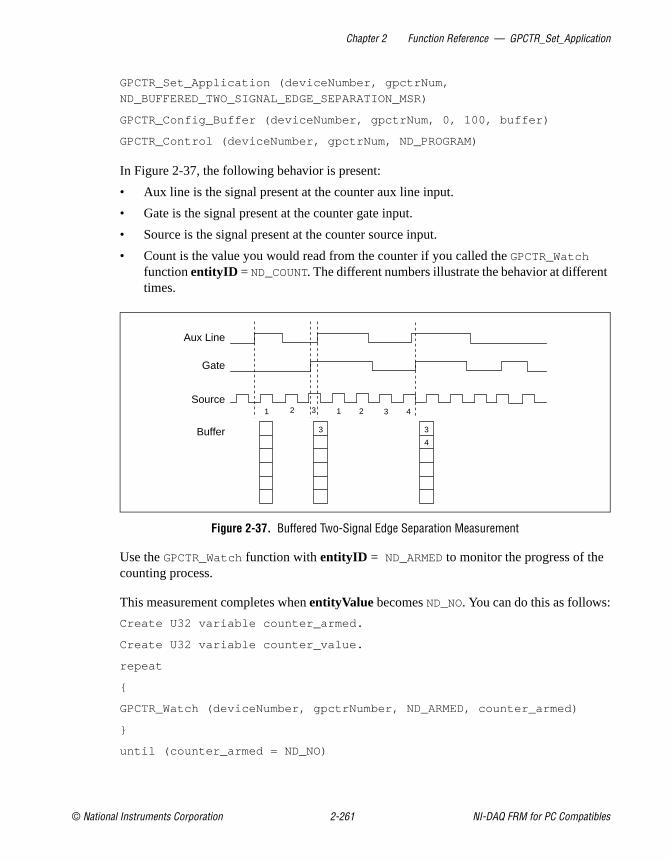
Chapter 2 Function Reference — GPCTR_Set_Application
© National Instruments Corporation 2-261 NI-DAQ FRM for PC Compatibles
GPCTR_Set_Application (deviceNumber, gpctrNum,
ND_BUFFERED_TWO_SIGNAL_EDGE_SEPARATION_MSR)
GPCTR_Config_Buffer (deviceNumber, gpctrNum, 0, 100, buffer)
GPCTR_Control (deviceNumber, gpctrNum, ND_PROGRAM)
In Figure 2-37, the following behavior is present:
• Aux line is the signal present at the counter aux line input.
• Gate is the signal present at the counter gate input.
• Source is the signal present at the counter source input.
• Count is the value you would read from the counter if you called the GPCTR_Watch function entityID = ND_COUNT. The different numbers illustrate the behavior at different times.
Figure 2-37. Buffered Two-Signal Edge Separation Measurement
Use the GPCTR_Watch function with entityID = ND_ARMED to monitor the progress of the counting process.
This measurement completes when entityValue becomes ND_NO. You can do this as follows:
Create U32 variable counter_armed.
Create U32 variable counter_value.
repeat
GPCTR_Watch (deviceNumber, gpctrNumber, ND_ARMED, counter_armed)
until (counter_armed = ND_NO)
Source
Buffer
3
Gate
Aux Line
1 2 3 41 2
3 3
4

Chapter 2 Function Reference — GPCTR_Set_Application
NI-DAQ FRM for PC Compatibles 2-262 www.natinst.com
When the counter is disarmed you can safely access data in the buffer. Another approach to accessing the data in the buffer while the counter is running is to use the GPCTR_Read_Buffer .
Typically, modifying the following parameters through the GPCTR_Change_Parameter function is useful when the counter application is ND_BUFFERED_TWO_SIGNAL_EDGE_SEPARATION_MSR. You can change the following:
• ND_SOURCE to ND_INTERNAL_100_KHZ. With this timebase, you can measure intervals between 20 µs and 11.37 hours long. The timing resolution will be lower than that you obtain using ND_INTERNAL_20_MHZ timebase. For NI-TIO based devices, use ND_INTERNAL_MAX_TIMEBASE for higher resolution.
• ND_AUX_LINE to any legal value listed in the GPCTR_Change_Parameter function description.
• ND_AUX_LINE_POLARITY to ND_NEGATIVE. Measurement will start on a falling edge.
• ND_GATE to any legal value listed in the GPCTR_Change_Parameter function description.
• ND_GATE_POLARITY to ND_NEGATIVE. Measurement stops on a falling edge.
• ND_BUFFER_MODE to ND_CONTINUOUS for circular buffer operations.
application = ND_BUFFERED_POSITION_MSR (NI-TIO based devices only)In this application, the counter is used to record the position of a motion encoder. The position of the motion encoder is latched or saved into a buffer upon a signal from the selected gate. This application works with two types of encoders: quadrature encoders (X1, X2, and X4), and two-pulse encoders (also referred to as up/down encoders).
Encoders generally have three channels: channels A, B, and Z. Two-pulse encoders do not use the Z channel. The A channel is hardwired to the default counter source pin. The B channel is hardwired to the aux line pin. Finally, the Z channel is hardwired to the gate pin.
The selected source for the counter determines the timebase of the counter during the position measurement. The selected source of the counter is set at the maximum internal timebase for the best resolution. The selected gate is used to trigger the counter into latching or saving the position of the encoder. The position of the encoder is saved into the specified buffer. By default, the selected gate is set to the default gate pin. However, you can set the selected gate to some other pin, too.
Some quadrature encoders have a third channel: channel Z. Channel Z is also referred to as the index channel. A high level on channel Z causes the counter to be reloaded with a specified value in the phase when A and B are high. You must ensure that channel Z is high during at least a portion of the phase when channel A and B are high. Otherwise, the GPCTR_Change_Parameter with paramID = ND_Z_INDEX_ACTIVE and paramValue = ND_YES. To set the reload value call GPCTR_Change_Parameter with paramID = ND_Z_INDEX_VALUE and paramValue = desired reload value.

Chapter 2 Function Reference — GPCTR_Set_Application
© National Instruments Corporation 2-263 NI-DAQ FRM for PC Compatibles
Figure 2-38 shows an example of X4 decoding. The reload of the counter occurs when all three channels are high. Also, the actual reload occurs within one max-timebase period after the reload phase becomes true. After the reload occurs, the counter continues to count from the specified reload value.
Figure 2-38. Buffered Position Measurement
Typically, you will find modifying the following parameters through the GPCTR_Change_Parameter function useful when the counter application is ND_POSITION_MSR. You can change the following:
• ND_Z_INDEX_ACTIVE to ND_YES to active the Z channel.
• ND_Z_INDEX_VALUE to the desired value for Z indexing.
• ND_INITIAL_COUNT to the desired initial value of the counter.
• ND_GATE to select which signal will trigger counter latches.
• ND_GATE_POLARITY TO ND_NEGATIVE. This will only affect the selected gate—not the hardwired Z index signal.
Note For 455X devices, this application cannot be used with counters 0 and 1.
5 6 87A=1B=1Z=1
2109 3 4
Ch A
Ch B
Ch ZMax Time Base
Counter Value
Selected Gate
Buffer6 6
1614
6145

Chapter 2 Function Reference — GPCTR_Watch
NI-DAQ FRM for PC Compatibles 2-264 www.natinst.com
GPCTR_Watch
Formatstatus = GPCTR_Watch (deviceNumber, gpctrNum, entityID, entityValue)
PurposeMonitors state of the general-purpose counter and its operation.
ParametersInput
Output
Parameter DiscussionLegal ranges for the gpctrNum, entityID , and entityValue are in terms of constants defined in a header file. The header file you should use depends on which of the following languages you are using:
• C programmers—NIDAQCNS.H (DATAACQ.H for LabWindows/CVI)
• BASIC programmers—NIDAQCNS.INC. (Visual Basic for Windows programmers should refer to the Programming Language Considerations section in Chapter 1, Using the NI-DAQ Functions, for more information.)
• Pascal programmers—NIDAQCNS.PAS
gpctrNum indicates which counter to program. The legal values for this parameter shown in Table 2-13.
entityID indicates which feature you are interested in. Legal values are listed in the following paragraphs, along with the corresponding values you can expect for entityValue. entityValue will be given either in terms of constants from the header file, or as numbers, as appropriate.
Name Type Description
deviceNumber i16 assigned by configuration utility
gpctrNum u32 number of the counter to use
entityID u32 identification of the feature to monitor
Name Type Description
entityValue *u32 the value of the feature specified by entityID

Chapter 2 Function Reference — GPCTR_Watch
© National Instruments Corporation 2-265 NI-DAQ FRM for PC Compatibles
entityID = ND_COUNT
This is the counter contents. entityValue can be between 0 and 224 – 1 for E Series, 671X, and 445X and between 0 and 232 – 1 for NI-TIO based devices. Reading the count while the counter is in progress does not affect the operation of the counter.
entityID = ND_AVAILABLE_POINTS
If the application is buffered event counting or time measurement, this entityID allows you to see how many points have been transferred to the buffer.
entityID = ND_ARMED
Indicates whether the counter is armed. entityValue can be ND_YES or ND_NO. You can use this in any counter operation for finding out when the operation completes.
entityID = ND_TC_REACHED
Indicates whether the counter has reached terminal count entityValue can be ND_YES or ND_NO. You can use this in time measurement applications for detecting overflow (pulse was too long to be measured using the selected timebase).
entityID = ND_OUTPUT_STATE
You can use this to read the value of the counter output; the range is ND_LOW and ND_HIGH.
entityID = ND_READ_MARK Indicates the read mark in the buffer when a continuous-buffer operation is in progress. entityValue can be between 0 and 232 – 1.
entityID = ND_WRITE_MARK Indicates the location in the buffer (specified in GPCTR_Config_Buffer ) in which the latest input data has been written. entityValue can be between 0 and 232 – 1.
entityID = ND_INTERNAL_MAX_TIMEBASE Indicates the maximum frequency of the timebase available for a counter. The entityValue is in Hertz. If gpctrNum = ND_RTC_X and the maximum timebase is greater than 50 MHz, this timebase cannot be selected as a source.
entityID = ND_MAX_PRESCALE Indicates the maximum value of the prescale factor that can be applied to the source selection of a NI-TIO-based device.
entityID = ND_READ_MARK_H_SNAPSHOT and ND_READ_MARK_L_SNAPSHOT
These attributes are set when GPCTR_Control is called with ND_SNAPSHOT. They return a 64-bit read offset for the current acquisition. ND_READ_MARK_H_SNAPSHOT is the upper four bytes, and ND_READ_MARK_L_SNAPSHOT is the lower four bytes.
entityID = ND_WRITE_MARK_H_SNAPSHOT and ND_WRITE_MARK_L_SNAPSHOT
These attributes are set when GPCTR_Control is called with ND_SNAPSHOT. They return a 64-bit write offset for the current acquisition. ND_WRITE_MARK_H_SNAPSHOT is the upper four bytes, and ND_WRITE_MARK_L_SNAPSHOT is the lower four bytes.

Chapter 2 Function Reference — GPCTR_Watch
NI-DAQ FRM for PC Compatibles 2-266 www.natinst.com
entityID = ND_BACKLOG_H_SNAPSHOT and ND_BACKLOG_L_SNAPSHOT
These attributes are set when GPCTR_Control is called with ND_SNAPSHOT. They return a 64-bit backlog total for the current acquisition. ND_BACKLOG_H_SNAPSHOT is the upper four bytes, and ND_BACKLOG_L_SNAPSHOT is the lower four bytes.
entityID = ND_ARMED_SNAPSHOT
This attribute returns the armed status of the counter acquisition during the last GPCTR_Control call with ND_SNAPSHOT. entityValue can be ND_YES or ND_NO.
entityID = ND_SAVED_COUNT (NI-TIO based devices only)This attribute returns the value of the latched hardware save register. This is handy for reading the last value latched by a gate signal.
entityID = ND_BUFFER_SIZE
This attribute returns the number of elements in the previously set buffer.
entityID = ND_ELEMENT_SIZE
This attribute returns the size of a buffer element in bytes.
Note C Programmers—entityValue is a pass-by-address parameter.
This function can report multiple errors. There are three types of errors that this function can report. Here are the rules of precedence:
• Miscellaneous Errors—These types of errors such as invalid errors will typically prevent the function from operating. These types of errors are reported over all other types of errors.
• overWriteError —This error can be reported during buffered operations. It indicates that the user did not read data from the buffer quickly enough and data was overwritten. If miscellaneous error occurs repeatedly during a read function, this can cause an overWriteError . The miscellaneous errors will be reported over the overWriteError . However, the overWriteError will be reported the next time a miscellaneous error does not occur during a GPCTR_Watch or GPCTR_Read call. Finally, the overWriteError is only issued once per overwrite. If one or more over write errors occur, then one over write error will be issued during the next GPCTR_Watch or GPCTR_Read call.
• dataLossError—This error can be reported during buffered operations. It indicates that the internal counter FIFO overflowed. Once this errors occurs, it is repeatedly reported until the end of the acquisition. All subsequent GPCTR_Watch and GPCTR_Read calls will return this error. Any other error will be reported over a dataLossError.

Chapter 2 Function Reference — ICTR_Read
© National Instruments Corporation 2-267 NI-DAQ FRM for PC Compatibles
ICTR_Read
Formatstatus = ICTR_Read (deviceNumber, ctr, count)
PurposeReads the current contents of the selected counter without disturbing the counting process and returns the count.
ParametersInput
Output
Parameter Discussionctr is the counter number.Range: 0 through 2.
count returns the current count of the specified counter while the counter is counting down. count can be between 0 and 65,535 when ctr is configured in binary mode (the default). count can be between 0 and 9,999 if the last call to ICTR_Setup configured ctr in BCD counting mode.
Note C Programmers—count is a pass-by-address parameter.
Name Type Description
deviceNumber i16 assigned by configuration utility
ctr i16 counter number
Name Type Description
count *u16 current count

Chapter 2 Function Reference — ICTR_Read
NI-DAQ FRM for PC Compatibles 2-268 www.natinst.com
Note BASIC Programmers—NI-DAQ returns count as a 16-bit unsigned number. In BASIC, integer variables are represented by a 16-bit two’s complement system. Thus, values greater than 32,767 are incorrectly treated as negative numbers when displaying. You can avoid this problem by using a long number as shown:
if count% < zero then
lcount& = count% + 65,536
else
lcount& = count%
end if

Chapter 2 Function Reference — ICTR_Reset
© National Instruments Corporation 2-269 NI-DAQ FRM for PC Compatibles
ICTR_Reset
Formatstatus = ICTR_Reset (deviceNumber, ctr, state)
PurposeSets the output of the selected counter to the specified state.
ParametersInput
Parameter Discussionctr is the counter number.Range: 0 through 2.
state is the logic state to which the counter is to be reset.Range: 0 or 1.
If state is 0, the counter output is forced low by programming the specified counter in mode 0. NI-DAQ does not load the count register; thus, the output remains low until NI-DAQ programs the counter in another mode. If state is 1, NI-DAQ forces the counter output high by programming the given counter in mode 2. NI-DAQ does not load the count register; thus, the output remains high until NI-DAQ programs the counter in another mode.
Name Type Description
deviceNumber i16 assigned by configuration utility
ctr i16 counter number
state i16 logic state to be reset

Chapter 2 Function Reference — ICTR_Setup
NI-DAQ FRM for PC Compatibles 2-270 www.natinst.com
ICTR_Setup
Formatstatus = ICTR_Setup (deviceNumber, ctr, mode, count, binBcd)
PurposeConfigures the given counter to operate in the specified mode.
ParametersInput
Parameter Discussionctr is the counter number.Range: 0 through 2.
mode is the mode in which the counter is to operate.0: Toggle output from low to high on terminal count.1: Programmable one-shot.2: Rate generator.3: Square wave rate generator.4: Software-triggered strobe.5: Hardware-triggered strobe.
In mode 0, the output goes low after the mode set operation, and the counter begins to count down while the gate input is high. The output goes high when NI-DAQ reaches the terminal count (that is, the counter has decremented to zero) and stays high until you set the selected counter to a different mode. Figure 2-39 shows the mode 0 timing diagram.
Name Type Description
deviceNumber i16 assigned by configuration utility
ctr i16 counter number
mode i16 mode in which the counter is to operate
count u16 period from one output pulse to the next
binBcd i16 16-bit binary or 4-decade binary-coded decimal

Chapter 2 Function Reference — ICTR_Setup
© National Instruments Corporation 2-271 NI-DAQ FRM for PC Compatibles
Figure 2-39. Mode 0 Timing Diagram
In mode 1, the output goes low on the count following the rising edge of the gate input and goes high on terminal count. Figure 2-40 shows the mode 1 timing diagram.
Figure 2-40. Mode 1 Timing Diagram
In mode 2, the output goes low for one period of the clock input. count indicates the period from one output pulse to the next. Figure 2-41 shows the mode 2 timing diagram.
Figure 2-41. Mode 2 Timing Diagram
Clock
WR
Gate
Output
6 5 4 3 2 1 0
(n = 6)
A BA + B = n
Clock
Gate
Output n = 4
4 3 2 1 0
WR
Clock
Output
Gate4 23 1 0 (4) 3 2 1
n = 4
0 (4)

Chapter 2 Function Reference — ICTR_Setup
NI-DAQ FRM for PC Compatibles 2-272 www.natinst.com
In mode 3, the output stays high for one half of the count clock pulses and stays low for the other half. Figure 2-42 shows the mode 3 timing diagram.
Figure 2-42. Mode 3 Timing Diagram
In mode 4, the output is initially high, and the counter begins to count down while the gate input is high. On terminal count, the output goes low for one clock pulse, then goes high again. Figure 2-43 shows the mode 4 timing diagram.
Figure 2-43. Mode 4 Timing Diagram
Mode 5 is similar to mode 4 except that the gate input is used as a trigger to start counting. Figure 2-44 shows the mode 5 timing diagram.
Figure 2-44. Mode 5 Timing Diagram
Output (n=5)
Gate
Output (n=4)
Gate
Clock
5 4 2 5 4 25
4 2 4 2 4 2 4 42
2
Clock
WR
Gate
Output
n = 4
4 3 2 1 0
Clock
Gate
WR
Output4 3 2 1 0
n = 2

Chapter 2 Function Reference — ICTR_Setup
© National Instruments Corporation 2-273 NI-DAQ FRM for PC Compatibles
See the 8253 Programmable Interval Timer data sheet in your DAQCard-500/700 or Lab and 1200 Series user manual for a detailed description of these modes and the associated timing diagrams.
count is the period from one output pulse to the next.Range for modes 0, 1, 4 and 5:
0 through 65,535 in binary counter operation.0 through 9,999 in BCD counter operation.
Range for modes 2 and 3:2 through 65,535 and 0 in binary counter operation.2 through 9,999 and 0 in BCD counter operation.
Note Zero is equivalent to 65,536 in binary counter operation and 10,000 in BCD counter operation.
Note BASIC Programmers—NI-DAQ passes count as a 16-bit unsigned number. In BASIC, integer variables are represented by a 16-bit two’s complement system. Thus, count values greater than 32,767 must be passed as negative numbers. One way to obtain the count value to be passed is to assign the required number between zero and 65,535 to a long variable and then obtain count as shown below:
count% = lcount& - 65,536
binBcd controls whether the counter operates as a 16-bit binary counter or as a 4-decade binary-coded decimal (BCD) counter.
0: 4-decade BCD counter.1: 16-bit binary counter.

Chapter 2 Function Reference — Init_DA_Brds
NI-DAQ FRM for PC Compatibles 2-274 www.natinst.com
Init_DA_Brds
Formatstatus = Init_DA_Brds (deviceNumber, deviceNumberCode)
PurposeInitializes the hardware and software states of a National Instruments DAQ device to its default state, and then returns a numeric device code that corresponds to the type of device initialized. Any operation that the device is performing is halted.
ParametersInput
Output
Parameter DiscussiondeviceNumberCode indicates the type of device initialized.
–1: Not a National Instruments DAQ device.7: PC-DIO-24.8: AT-DIO-32F.
12: PC-DIO-96.13: PC-LPM-16.14: PC-TIO-10.15: AT-AO-6.25: AT-MIO-16E-2.26: AT-AO-10.27: AT-A2150C.28: Lab-PC+.30: SCXI-1200.31: DAQCard-700.32: NEC-MIO-16E-4.33: DAQPad-1200.35: DAQCard-DIO-24.36: AT-MIO-16E-10.
Name Type Description
deviceNumber i16 assigned by configuration utility
Name Type Description
deviceNumberCode *i16 type of device
Chapter 2 Function Reference — Init_DA_Brds
© National Instruments Corporation 2-275 NI-DAQ FRM for PC Compatibles
37: AT-MIO-16DE-10.38: AT-MIO-64E-3.39: AT-MIO-16XE-50.40: NEC-AI-16E-4.41: NEC-MIO-16XE-50.42: NEC-AI-16XE-50.43: DAQPad-MIO-16XE-50.44: AT-MIO-16E-1.45: PC-OPDIO-16.46: PC-AO-2DC.47: DAQCard-AO-2DC.48: DAQCard-1200.49: DAQCard-500.50: AT-MIO-16XE-10.51: AT-AI-16XE-10.52: DAQCard-AI-16XE-50.53: DAQCard-AI-16E-4.54: DAQCard-516.55: PC-516.56: PC-LPM-16PnP.57: Lab-PC-1200.58: Lab-PC-1200AI.59: VXI-MIO-64E-1.60: VXI-MIO-64XE-10.61: VXI-AO-48XDC.62: VXI-DIO-128.65: PC-DIO-24PnP.66: PC-DIO-96PnP.67: AT-DIO-32HS.68: PXI-6533.75: DAQPad-6507/6508.76: DAQPad-6020E for USB.88: DAQCard-6062E.90: DAQCard-6023E.91: DAQCard-6024E.
200: PCI-DIO-96.201: PCI-1200.202: PCI-MIO-16XE-50.204: PCI-MIO-16XE-10.205: PCI-MIO-16E-1.206: PCI-MIO-16E-4.207: PXI-6070E.208: PXI-6040E.209: PXI-6030E.

Chapter 2 Function Reference — Init_DA_Brds
NI-DAQ FRM for PC Compatibles 2-276 www.natinst.com
210: PXI-6011E.211: PCI-DIO-32HS.215: DAQCard-6533.220: PCI-6031E (MIO-64XE-10).221: PCI-6032E (AI-16XE-10).222: PCI-6033E (AI-64XE-10).223: PCI-6071E (MIO-64E-1).232: PCI-6602.233: PCI-4451.234: PCI-4452.235: NI 4551.236: NI 4552.237: PXI-6602.240: PXI-6508.241: PCI-6110E.244: PCI-6111E.256: PCI-6503.261: PCI-6711.262: PXI-6711.263: PCI-6713.264: PXI-6713.265: PCI-6704.266: PXI-6704.267: PCI-6023E.268: PXI-6023E.269: PCI-6024E.270: PXI-6024E.271: PCI-6025E.272: PXI-6025E.273: PCI-6052E.274: PXI-6052E.275: DAQPad-6070E.276: DAQPad-6052E.285: PCI-6527.286: PXI-6527.308: PCI-6601.311: PCI-6703.314: PCI-6034E.315: PXI-6034E.316: PCI-6035E.

Chapter 2 Function Reference — Init_DA_Brds
© National Instruments Corporation 2-277 NI-DAQ FRM for PC Compatibles
317: PXI-6035E.318: PXI-6703.319: PXI-6608.320: PCI-4453.321: PCI-4454.
Note C Programmers—deviceNumberCode is a pass-by-address parameter.
Using This FunctionInit_DA_Brds is called automatically and does not have to be explicitly called by your application. This function is useful for reinitializing the device hardware, for reinitializing the NI-DAQ software, and for determining which device has been assigned to a particular slot number. Init_DA_Brds clears all configured messages for the device just as if you called Config_DAQ_Event_Message with a mode of 0. Init_DA_Brds initializes a device in a specified slot to the default conditions. These conditions are summarized for each device as follows:
• MIO and AI devices
– Analog Input defaults:
number of channels = 2.
Mode = Differential.
Range = 20 V (10 V for 12-bit E Series).
Polarity = Bipolar (–10 V to +10 V for PCI-6110E, PCI-6111E, and all 16-bit E Series devices, except the 6052E; and –5 to +5 V for all other devices).
External conversion = Disabled.
Start trigger = Disabled.
Stop trigger = Disabled.
Coupling = DC coupling.
– Analog Output defaults (MIO and 671X devices only):
Range = 20 V.
Reference = 10 V.
Mode = Bipolar (–10 to +10 V).
Level = 0 V.
– Digital Input and Output defaults:
Direction = Input.
For ports 2, 3, and 4 of the 6052E devices and AT-MIO-16DE-10, see also the default conditions of ports 0, 1, and 2 of the DIO-24 (6503).

Chapter 2 Function Reference — Init_DA_Brds
NI-DAQ FRM for PC Compatibles 2-278 www.natinst.com
• DIO-24 (6503)/DIO-32F/DIO 6533 (DIO-32HS)/DIO-96
– Digital Input and Output defaults:
Direction = Input.
Handshaking = Disabled.
Group assignments = No ports assigned to any group.
• PC-TIO-10
– Digital Input and Output defaults:
Mode = Differential.
Direction = Input.
– Counter/Timer defaults:
Gating mode = No gating.
Output type = Terminal count toggled.
Output polarity = Positive.
Edge mode = Count rising edges.
Count mode = Count once.
Output level = Off.
• 660X devices
– Counter/Timer defaults:
Gating mode = Depends on the type of counter application.
Counter output type = Terminal count toggled.
Output value = Logic low.
Default polarity (gates, sources, outputs) = Active high.
Default internal timebase = 20 MHz.
Digital debouncing filters = Disabled.
Pad synchronization = Disabled.
Prescalers = Disabled.
– Digital Input and Output defaults:
Direction =Input.
• VXI-DIO-128
– Digital Input and Output defaults:
Direction = Input (ports 0 through 7).
Direction = Output (ports 8 through 15).
Input ports logic threshold: 1500 mV.

Chapter 2 Function Reference — Init_DA_Brds
© National Instruments Corporation 2-279 NI-DAQ FRM for PC Compatibles
• VXI-AO-48XDC
– Analog Output defaults:
Mode = Bipolar (–10 to 10 V).
– Digital Input and Output defaults:
Direction = Input.
Range = 20 V.
Reference = 10 V.
• Lab and 1200 Series devices
– Analog Input defaults:
Input mode = Single-ended (eight single-ended input channels).
Polarity = Bipolar (–5 to +5 V).
External conversion = Disabled.
Start trigger = Disabled.
External conversion = Stop trigger = Disabled.
– Analog Output defaults:
Mode = Bipolar (–5 to +5 V).
Range = 20 Level = 0 V.
– Digital Input and Output defaults:
Direction = Input.
Handshaking = Disabled.
Group assignments = No ports assigned to any group.
– Counter/Timer defaults:
Output level = Logical low.
• 516 and LPM devices and DAQCard-500/700
– Analog Input default:
Mode = Single-ended (Differential also possible for 516 devices and DAQCard-700).
Reference = Range = 10 V.
Polarity = Bipolar (–5 to +5 V).
Stop trigger = External conversion = Disabled.
Mode = Differential.
Calibrated.

Chapter 2 Function Reference — Init_DA_Brds
NI-DAQ FRM for PC Compatibles 2-280 www.natinst.com
– Digital Input and Output defaults:
Output port voltage level = 0 V.
– Counter/Timer defaults:
Output level = Logical low.
• AT-AO-6/10
– Analog Output defaults:
Range = 20 V.
Reference = 10 V.
Mode = Bipolar (–10 to +10 V).
Level = 0 V.
Group assignments = No channels assigned to any group.
Digital input and output defaults direction = Input.
Translate and demux = Disabled.
• AO-2DC devices
– Analog Output defaults:
Mode = Unipolar (0 to 10 V).
Level = 0 V.
– Digital Input and Output defaults:
Direction = Input.
• DSA devices
– Analog Input defaults:
Gain = 0 dB.
Coupling = AC coupling.
Start Trigger = Automatic.
Stop Trigger = Disabled.
– Analog Output defaults:
Attenuation = 0 dB.
Output Enable = Off.
– Digital Input and Output defaults:
Direction = Input.

Chapter 2 Function Reference — Init_DA_Brds
© National Instruments Corporation 2-281 NI-DAQ FRM for PC Compatibles
• 6703 devices:
– Analog Output defaults:
Voltage Outputs = at user defined levels.
– Digital Input and Output defaults:
Direction = Input.
• 6704 devices:
– Analog Output defaults:
Voltage Outputs = at user defined levels.
Current Outputs = at user defined levels.
– Digital Input and Output defaults:
Direction = Input.
Of all these defaults, you can alter only the analog input and analog output settings of the Lab-PC+ and PC-LPM-16 devices by setting jumpers on the device. If you change the jumpers from the factory settings, you must call either AI_Configure and/or AO_Configure after Init_DA_Brds so that the software copies of these settings reflect the true settings of the device.
If any device resources have been reserved for SCXI use when you make a call to Init_DA_Brds , those resources will still be reserved after you make the function call. Refer to Chapter 12, SCXI Hardware, in the DAQ Hardware Overview Guide for listings of the different device resources that can be reserved for SCXI.

Chapter 2 Function Reference — Lab_ISCAN_Check
NI-DAQ FRM for PC Compatibles 2-282 www.natinst.com
Lab_ISCAN_Check
Formatstatus = Lab_ISCAN_Check (deviceNumber, daqStopped, retrieved, finalScanOrder)
PurposeChecks whether the current multiple-channel scanned data acquisition begun by the Lab_ISCAN_Start function is complete and returns the status, the number of samples acquired to that point, and the scanning order of the channels in the data array (DAQCard-500/700 and 516, Lab and 1200 Series, and LPM devices only).
ParametersInput
Output
Parameter DiscussiondaqStopped returns an indication of whether the data acquisition has completed.
1: The data acquisition operation has stopped. Either NI-DAQ has acquired all the samples or an error has occurred.
0: The data acquisition operation is not yet complete.
retrieved indicates the progress of an acquisition. The meaning of retrieved depends on whether you have enabled pretrigger mode (see DAQ_StopTrigger_Config ).
If pretrigger mode is disabled, retrieved returns the number of samples collected by the acquisition at the time of the call to Lab_ISCAN_Check . The value of retrieved increases until it equals the total number of samples to be acquired, at which time the acquisition terminates.
Name Type Description
deviceNumber i16 assigned by configuration utility
Name Type Description
daqStopped *i16 indicates whether the data acquisition has completed
retrieved *u32 number of samples collected by the acquisition
finalScanOrder [i16] the scan channel order

Chapter 2 Function Reference — Lab_ISCAN_Check
© National Instruments Corporation 2-283 NI-DAQ FRM for PC Compatibles
However, if pretrigger mode is enabled, retrieved returns the offset of the position in your buffer where NI-DAQ places the next data point when the function acquires. After the value of retrieved reaches count – 1 and rolls over to 0, the acquisition begins to overwrite old data with new data. When you apply a signal to the stop trigger input, the acquisition collects an additional number of samples specified by ptsAfterStoptrig in the call to DAQ_StopTrigger_Config and then terminates. When Lab_ISCAN_Check returns a status of 1, retrieved contains the offset of the oldest data point in the array (assuming that the acquisition has written to the entire buffer at least once). In pretrigger mode, Lab_ISCAN_Check automatically rearranges the array upon completion of the acquisition so that the oldest data point is at the beginning of the array. Thus, retrieved always equals 0 upon completion of a pretrigger mode acquisition. Because the stop trigger can occur in the middle of a scan sequence, the acquisition can end in the middle of a scan sequence. So, when the function rearranges the data in the buffer, the first sample might not belong to the first channel in the scan sequence. You can examine the finalScanOrder array to find out the way the data is arranged in the buffer.
finalScanOrder is an array that indicates the scan channel order of the data in the buffer passed to Lab_ISCAN_Start . The size of finalScanOrder must be at least equal to the number of channels scanned. This parameter is valid only when NI-DAQ returns daqStopped as 1 and is useful only when you enable pretrigger mode (Lab and 1200 Series devices only).
If you do not use pretrigger mode, the values contained in finalScanOrder are, in single-ended mode, n–1, n-2,...1, 0 to 0, in that order, and in differential mode, 2*(n–1), 2*(n–2),..., 2, 0, in that order, where n is the number of channels scanned. For example, if you scanned three channels in single-ended mode, the finalScanOrder returns:
finalScanOrder[0] = 2.finalScanOrder[1] = 1.finalScanOrder[2] = 0.
So the first sample in the buffer belongs to channel 2, the second sample belongs to channel 1, the third sample belong to channel 0, the fourth sample belongs to channel 2, and so on. This is the scan order expected from the Lab-PC+ and finalScanOrder is not useful in this case.
If you use pretrigger mode, the order of the channel numbers in finalScanOrder depends on where in the scan sequence the acquisition ended. This can vary because the stop trigger can occur in the middle of a scan sequence, which would cause the acquisition to end in the middle of a scan sequence so that the oldest data point in the buffer can belong to any channel in the scan sequence. Lab_ISCAN_Check rearranges the buffer so that the oldest data point is at index 0 in the buffer. This rearrangement causes the scanning order to change. This new scanning order is returned by finalScanOrder. For example, if you scanned three channels, the original scan order is channel 2, channel 1, channel 0, channel 2, channel 1, channel 0, and

Chapter 2 Function Reference — Lab_ISCAN_Check
NI-DAQ FRM for PC Compatibles 2-284 www.natinst.com
so on. However, after the stop trigger, if the acquisition ends after taking a sample from channel 1, the oldest data point belongs to channel 0. So finalScanOrder returns:
finalScanOrder[0] = 0.finalScanOrder[1] = 2.finalScanOrder[2] = 1.
So the first sample in the buffer belongs to channel 0, the second sample belongs to channel 2, the third sample belongs to channel 1, the fourth sample belongs to channel 0, and so on.
Note C Programmers—daqStopped and retrieved are pass-by-address parameters.
Using This FunctionLab_ISCAN_Check checks the current background data acquisition operation to determine whether it has completed and returns the number of samples acquired at the time that you called Lab_ISCAN_Check . If the operation is complete, Lab_ISCAN_Check sets daqStopped = 1. Otherwise, daqStopped is set to 0. Before Lab_ISCAN_Check returns daqStopped = 1, it calls DAQ_Clear , allowing another Start call to execute immediately.
If Lab_ISCAN_Check returns an overFlowError or an overRunError , NI-DAQ has terminated the data acquisition operation because of lost A/D conversions due to a sample rate that is too high (sample interval was too small). An overFlowError indicates that the A/D FIFO memory overflowed because the data acquisition servicing operation was not able to keep up with sample rate. An overRunError indicates that the data acquisition circuitry was not able to keep up with the sample rate. Before returning either of these error codes, Lab_ISCAN_Check calls DAQ_Clear to terminate the operation and reinitialize the data acquisition circuitry.

Chapter 2 Function Reference — Lab_ISCAN_Op
© National Instruments Corporation 2-285 NI-DAQ FRM for PC Compatibles
Lab_ISCAN_Op
Formatstatus = Lab_ISCAN_Op (deviceNumber, numChans, gain, buffer, count, sampleRate, scanRate,
finalScanOrder)
PurposePerforms a synchronous, multiple-channel scanned data acquisition operation. Lab_ISCAN_Op does not return until NI-DAQ has acquired all the data or an acquisition error has occurred (DAQCard-500/700 and 516, Lab and 1200 Series, and LPM devices only).
ParametersInput
Output
Input/Output
Parameter DiscussionnumChans is the number of channels to be scanned in a single scans sequence. The value of this parameter also determines which channels NI-DAQ scans because these devices have a fixed scanning order. The scanned channels range from numChans – 1 to channel 0. If you are using SCXI modules with additional multiplexers, you must scan the analog input
Name Type Description
deviceNumber i16 assigned by configuration utility
numChans i16 number of channels to be scanned
gain i16 gain setting
count u32 number of samples to be acquired
sampleRate f64 desired sample rate in units of pts/s
scanRate f64 desired scan rate in units of scans/s
Name Type Description
finalScanOrder [i16] the scan channel order of the data
Name Type Description
buffer [i16] conversion samples returned

Chapter 2 Function Reference — Lab_ISCAN_Op
NI-DAQ FRM for PC Compatibles 2-286 www.natinst.com
channels on the DAQ device that corresponds to the SCXI channels you want. You should select the SCXI scan list using SCXI_SCAN_Setup before you call this function. Refer to theNI-DAQ User Manual for PC Compatibles for more information on SCXI channel assignments.Range: 1 through 4 for the 516 and Lab and 1200 Series devices in differential mode.
1 through 8 for DAQCard-500 (single-ended mode only).1 through 8 for DAQCard-700 in differential mode.1 through 8 for the Lab and 1200 Series devices in single-ended mode.1 through 16 for LPM devices or DAQCard-700 in single-ended mode.
gain is the gain setting to be used for the scanning operation. The same gain is applied to all the channels scanned. This gain setting applies only to the DAQ device; if you use SCXI modules with additional gain selection, you must establish any gain you want at the SCXI module either by setting jumpers on the module or by calling SCXI_Set_Gain . The following gain settings are valid for the Lab and 1200 Series devices—1, 2, 5, 10, 20, 50, and 100. If you use an invalid gain, NI-DAQ returns an error. NI-DAQ ignores gain for the DAQCard-500/700 and 516 and LPM devices.
buffer is an integer array. buffer must have a length not less than count. When Lab_ISCAN_Op returns with an error code of zero, buffer contains the acquired data.
count is the number of samples to be acquired (that is, the number of A/D conversions to be performed).Range: 3 through 232 – 1 (except Lab and 1200 Series devices, which are limited to
65,535).
sampleRate is the sample rate you want in units of pts/s.Range: Roughly 0.00153 pts/s through 62,500 pts/s (Lab and 1200 Series devices).
Roughly 0.00153 pts/s through 50,000 pts/s (DAQCard-500/700 and 516 and LPM devices).
Note If you are using an SCXI-1200 with remote SCXI, the maximum rate depends on the baud rate setting and count. Refer to the SCXI-1200 User Manual for more details.
scanRate is the scan rate you want in units of scans per second. This is the rate at which NI-DAQ performs scans. NI-DAQ performs a scan each time NI-DAQ samples all channels in the scan sequence. ScanRate must be slightly less than sampleRate/numChans due to a 5 µs delay interval to the driver. Lab_ISCAN interval scanning is available on the Lab and 1200 Series devices only.Range: 0 and roughly 0.00153 scans/s through 62,500 scans/s.
Note If you are using an SCXI-1200 with remote SCXI, the maximum rate depends on the baud rate setting and count. Refer to the SCXI-1200 User Manual for more details.

Chapter 2 Function Reference — Lab_ISCAN_Op
© National Instruments Corporation 2-287 NI-DAQ FRM for PC Compatibles
A value of 0 disables interval scanning.
finalScanOrder is an array that indicates the scan channel order of the data in the buffer passed to Lab_ISCAN_Op. The size of finalScanOrder must be at least equal to the number of channels scanned. This parameter is valid only when the error is returned to zero and is useful only when pretrigger mode is enabled (Lab and 1200 Series devices only).
If you do not use pretrigger mode, the values contained in finalScanOrder are, in single-ended mode, n–1, n–2, . . . , 1, 0, in that order, and in differential mode, 2 (n–1), 2 (n–2), . . . , 1, 0, in that order, where n is the number of channels scanned. For example, if you scanned three channels in single-ended mode, the finalScanOrder returns:
finalScanOrder[0] = 2.finalScanOrder[1] = 1.finalScanOrder[2] = 0.
So the first sample in the buffer belongs to channel 2, the second sample belongs to channel 1, the third sample belongs to channel 0, the fourth sample belongs to channel 2, and so on. This is exactly the scan order you would expect from the Lab and 1200 Series devices and finalScanOrder is not useful in this case.
If you use pretrigger mode, the order of the channel numbers in finalScanOrder depends on where in the scan sequence the acquisition ended. This can vary because the stop trigger can occur in the middle of a scan sequence, which causes the acquisition to end in the middle of a scan sequence so that the oldest data point in the buffer can belong to any channel in the scan sequence. Lab_ISCAN_Op rearranges the buffer so that the oldest data point is at index 0 in the buffer. This rearrangement causes the scanning order to change. This new scanning order is returned by finalScanOrder. For example, if you scanned three channels, the original scan order is channel 2, channel 1, channel 0, channel 2, and so on. However, after the stop trigger, if the acquisition ends after taking a sample from channel 1, the oldest data point belongs to channel 0.
So finalScanOrder returns:
finalScanOrder[0] = 0.finalScanOrder[1] = 2.
finalScanOrder[2] = 1.
Therefore the first sample in the buffer belongs to channel 0, the second sample belongs to channel 2, the third sample belongs to channel 1, the fourth sample belongs to channel 0, and so on.

Chapter 2 Function Reference — Lab_ISCAN_Op
NI-DAQ FRM for PC Compatibles 2-288 www.natinst.com
Using This FunctionLab_ISCAN_Op initiates a synchronous process of acquiring A/D conversion samples and storing them in a buffer. Lab_ISCAN_Op does not return control to your application until NI-DAQ acquires all the samples you want (or until an acquisition error occurs). When you use posttrigger mode, the process stores count A/D conversions in the buffer and ignores any subsequent conversions.
Note If you have selected external start triggering of the data acquisition operation, a low-to-high edge at the EXTTRIG of the Lab and 1200 Series device I/O connector input initiates the operation. Be aware that if you do not apply the start trigger, Lab_ISCAN_Op does not return control to your application. Otherwise, Lab_ISCAN_Op issues a software trigger to initiate the data acquisition operation.
If you have enabled pretrigger mode, the sample counter does not begin counting acquisitions until a signal is applied at the stop trigger input. Until this signal is applied, the acquisition remains in a cyclical mode, continually overwriting old data in the buffer with new data. Again, if the stop trigger is not applied, Lab_ISCAN_Op does not return control to your application.
In any case, you can use Timeout_Config to establish a maximum length of time for Lab_ISCAN_Op to execute.

Chapter 2 Function Reference — Lab_ISCAN_Start
© National Instruments Corporation 2-289 NI-DAQ FRM for PC Compatibles
Lab_ISCAN_Start
Formatstatus = Lab_ISCAN_Start (deviceNumber, numChans, gain, buffer, count, sampTimebase,
sampInterval, scanInterval)
PurposeInitiates a multiple-channel scanned data acquisition operation and stores its input in an array (DAQCard-500/700 and 516, Lab and 1200 Series, and LPM devices only).
ParametersInput
Input/Output
Parameter DiscussionnumChans is the number of channels to be scanned in a single scan sequence. The value of this parameter also determines which channels NI-DAQ scans because these supported devices have a fixed scanning order. The scanned channels range from numChans – 1 to channel 0. If you are using SCXI modules with additional multiplexers, you must scan the appropriate analog input channels on the DAQ device that corresponds to the SCXI channels you want. You should select the SCXI scan list using SCXI_SCAN_Setup before you call this function. Refer to Chapter 12, SCXI Hardware, in the DAQ Hardware Overview Guide and
Name Type Description
deviceNumber i16 assigned by configuration utility
numChans i16 number of channels to be scanned
gain i16 gain setting
count u32 total number of samples to be acquired
sampTimebase i16 timebase, or resolution, used for the sample interval counter
sampInterval u16 length of the sample interval
scanInterval u16 length of the scan interval
Name Type Description
buffer [i16] conversion samples returned
Chapter 2 Function Reference — Lab_ISCAN_Start
NI-DAQ FRM for PC Compatibles 2-290 www.natinst.com
the NI-DAQ User Manual for PC Compatibles for more information on SCXI channel assignments.Range: 1 through 4 for the 516 and Lab and 1200 Series devices in differential mode.
1 through 8 for the DAQCard-500 (single-ended mode only).1 through 8 for the DAQCard-700 in differential mode.1 through 8 for the 516 and Lab and 1200 Series devices in single-ended mode.1 through 16 for the DAQCard-700 and LPM devices in single-ended mode.
gain is the gain setting to be used for the scanning operation. NI-DAQ applies the same gain to all the channels scanned. This gain setting applies only to the DAQ device; if you are using SCXI modules with additional gain selection, you must establish any gain you want at the SCXI module either by setting jumpers on the module or by calling SCXI_Set_Gain . The following gain settings are valid for the Lab and 1200 Series devices: 1, 2, 5, 10, 20, 50, 100. If you use an invalid gain setting, NI-DAQ returns an error. NI-DAQ ignores gain for the DAQCard-500/700 and 516 and LPM devices.
buffer is an integer array. buffer must have a length equal to or greater than count.
count is the total number of samples to be acquired (that is, the number of A/D conversions to be performed). For double-buffered acquisitions, count must be even.Range: 3 through 232 – 1 (except the Lab and 1200 Series devices, which are limited to
65,535 unless enabled for double-buffered mode).
sampTimebase is the timebase, or resolution, to be used for the sample-interval counter. The sample-interval counter controls the time that elapses between acquisition of samples within a scan sequence.
sampTimebase has the following possible values:1: 1 MHz clock used as timebase (1 µs resolution).2: 100 kHz clock used as timebase (10 µs resolution).3: 10 kHz clock used as timebase (100 µs resolution).4: 1 kHz clock used as timebase (1 ms resolution).5: 100 Hz clock used as timebase (10 ms resolution).
If sample-interval timing is to be externally controlled, NI-DAQ ignores sampTimebase and the parameter can be any value.
sampInterval indicates the length of the sample interval (that is, the amount of time to elapse between each A/D conversion within a scan sequence).Range: 2 through 65,535.

Chapter 2 Function Reference — Lab_ISCAN_Start
© National Instruments Corporation 2-291 NI-DAQ FRM for PC Compatibles
The sample interval is a function of the timebase resolution. NI-DAQ determines the actual sample interval in seconds by the following formula:
sampInterval * (sample timebase resolution)
where the sample timebase resolution is equal to one of the values of sampTimebase as specified above. For example, if sampInterval = 25 and sampTimebase = 2, the actual sample interval is 25 * 10 µs = 250 µs. The total sample interval (the time to complete one scan sequence) in seconds is the actual sample interval * number of channels scanned. If the sample interval is to be externally controlled by conversion pulses applied to the EXTCONV* input, NI-DAQ ignores the sampInterval and the parameter can be any value.
scanInterval indicates the length of the scan interval. This is the amount of time to elapse between scans. The timebase for this parameter is actually the sampTimebase parameter. The function performs a scan each time NI-DAQ samples all channels in the scan sequence. Therefore, scanInterval must be greater than or equal to sampInterval * numChans +5 µs.Range: 0 and 2 through 65,535.
A value of 0 disables interval scanning. Lab_ISCAN interval scanning is not available on the DAQCard-500/700 and 516 and LPM devices.
Using This FunctionIf you did not specify external sample-interval timing by the DAQ_Config call, NI-DAQ sets the sample-interval counter to the specified sampInterval and sampTimebase, and sets the sample counter up to count the number of samples acquired and to stop the data acquisition process when the number of samples acquired equals count. If you have specified external sample-interval timing, the data acquisition circuitry relies on pulses received on the EXTCONV* input to initiate individual A/D conversions.
Lab_ISCAN_Start initializes a background data acquisition process to handle storing of A/D conversion samples into the buffer as NI-DAQ acquires them. When you use posttrigger mode (with pretrigger mode disabled), the process stores up to count A/D conversion samples into the buffer and ignores any subsequent conversions. The order of the scan is from channel n–1 to channel 0, where n is the number of channels being scanned. For example, if numChans is 3 (that is, you are scanning three channels), NI-DAQ stores the data in the buffer in the following order:
First sample from channel 2, first sample from channel 1, first sample from channel 0, second sample from channel 2, and so on.
You cannot make the second call to Lab_ISCAN_Start without terminating this background data acquisition process. If a call to Lab_ISCAN_Check returns daqStopped = 1, the samples are available and NI-DAQ terminates the process. In addition, a call to DAQ_Clear terminates the background data acquisition process. Notice that if a call to Lab_ISCAN_Check returns overFlowError or overRunError , or returns with daqStopped = 1, the process is automatically terminated and there is no need to call DAQ_Clear .

Chapter 2 Function Reference — Lab_ISCAN_Start
NI-DAQ FRM for PC Compatibles 2-292 www.natinst.com
For the Lab and 1200 Series devices, if you enable pretrigger mode, Lab_ISCAN_Start initiates a cyclical acquisition that continually fills the buffer with data, wrapping around to the start of the buffer once NI-DAQ has written to the entire buffer. When you apply the signal at the stop trigger input, Lab_ISCAN_Start acquires an additional number of samples specified by the ptsAfterStoptrig parameter in DAQ_StopTrigger_Config and then terminates.
Because the trigger can occur at any point in the scan sequence, the scanning operation can end in the middle of a scan sequence. See the description for Lab_ISCAN_Check to determine how NI-DAQ rearranges the buffer after the acquisition ends. When you enable pretrigger mode, the length of the buffer, which is greater than or equal to count, should be an integral multiple of numChans.
If you have selected external start triggering of the data acquisition operation, a low-to-high edge at the EXTTRIG of the Lab and 1200 Series device I/O connector input initiates the data acquisition operation after the Lab_ISCAN_Start call is complete. Otherwise, Lab_ISCAN_Start issues a software trigger to initiate the data acquisition operation before returning.
Note If your application calls Lab_ISCAN_Start , always make sure that you call DAQ_Clear before your application terminates and returns control to the operating system. Unless you make this call (either directly, or indirectly through Lab_ISCAN_Check or DAQ_DB_Transfer ), unpredictable behavior might result.

Chapter 2 Function Reference — Lab_ISCAN_to_Disk
© National Instruments Corporation 2-293 NI-DAQ FRM for PC Compatibles
Lab_ISCAN_to_Disk
Formatstatus = Lab_ISCAN_to_Disk (deviceNumber, numChans, gain, filename, count, sampleRate,
scanRate, concat)
PurposePerforms a synchronous, multiple-channel scanned data acquisition operation and simultaneously saves the acquired data in a disk file. Lab_ISCAN_to_Disk does not return until NI-DAQ has acquired and saved all the data or an acquisition error has occurred (DAQCard-500/700 and 516, Lab and 1200 Series, and LPM devices only).
ParametersInput
Parameter DiscussionnumChans is the number of channels to be scanned in a single scan sequence. The value of this parameter also determines which channels NI-DAQ scans because these supported devices have a fixed scanning order. The scanned channels range from numChans – 1 to channel 0. If you are using SCXI modules with additional multiplexers, you must scan the appropriate analog input channels on the DAQ device that corresponds to the SCXI channels you want. You should select the SCXI scan list using SCXI_SCAN_Setup before you call this function. Refer to Chapter 12, SCXI Hardware, in the DAQ Hardware Overview Guide and the NI-DAQ User Manual for PC Compatibles for more information on SCXI channel assignments.Range: 1 through 4 for the 516 and Lab and 1200 Series devices in differential mode.
1 through 8 for the DAQCard-500 (single-ended mode only).
Name Type Description
deviceNumber i16 assigned by configuration utility
numChans i16 number of channels to be scanned
gain i16 gain setting
filename STR name of the data file to be created
count u32 number of samples to be acquired
sampleRate f64 desired sample rate in units of points per second
scanRate f64 desired scan rate in units of points per second
concat i16 enables concatenation of data to an existing file

Chapter 2 Function Reference — Lab_ISCAN_to_Disk
NI-DAQ FRM for PC Compatibles 2-294 www.natinst.com
1 through 8 for the DAQCard-700 in differential mode.1 through 8 for the 516 and Lab and 1200 Series devices in single-ended mode.1 through 16 for the DAQCard-700 and LPM devices in single-ended mode.
gain is the gain setting to be used for the scanning operation. NI-DAQ applies the same gain to all the channels scanned. This gain setting applies only to the DAQ device; if you use SCXI modules with additional gain selection, you must establish any gain you want at the SCXI module either by setting jumpers on the module or by calling SCXI_Set_Gain . The following gain settings are valid for the Lab and 1200 Series devices: 1, 2, 5, 10, 20, 50, 100. If you use an invalid gain setting, NI-DAQ returns an error. NI-DAQ ignores gain for the DAQCard-500/700 and LPM devices.
count is the number of samples to be acquired (that is, the number of A/D conversions to be performed). The length of your data file should be exactly twice the value of count. If you have previously enabled pretrigger mode (by a call to DAQ_StopTrigger_Config ) NI-DAQ ignores the count parameter.Range: 3 through 232 – 1.
sampleRate is the sample rate you want in units of points per second.Range: Roughly 0.00153 pts/s through 62,500 pts/s (Lab and 1200 Series devices).
Roughly 0.00153 pts/s through 50,000 pts/s (DAQCard-500/700 and 516 and LPM devices).
Note If you are using an SCXI-1200 with remote SCXI, the maximum rate will depend on the baud rate setting and count. Refer to the SCXI-1200 User Manual for more details.
scanRate is the scan rate you want in units of points per second. This is the rate at which NI-DAQ performs scans. The function performs a scan each time NI-DAQ samples all channels in the scan sequence. Therefore, scanRate must be equal to or greater than (sampleRate)/(numChans). Lab_ISCAN interval scanning is available on the Lab and 1200 Series devices only.Range: 0 and roughly 0.00153 pts/s through 62,500 pts/s.
Note If you are using an SCXI-1200 with remote SCXI, the maximum rate will depend on the baud setting. Refer to the SCXI-1200 User Manual for more details.
A value of 0 disables interval scanning.
concat enables concatenation of data to an existing file. Regardless of the value of concat, if the file does not exist, NI-DAQ creates the file.
0: Overwrite file if it exists.1: Concatenate new data to an existing file.

Chapter 2 Function Reference — Lab_ISCAN_to_Disk
© National Instruments Corporation 2-295 NI-DAQ FRM for PC Compatibles
Using This FunctionLab_ISCAN_to_Disk initiates a synchronous process of acquiring A/D conversion samples and storing them in a disk file. Data is written to disk in a 16-bit binary format, with the lower byte first (little endian). Lab_ISCAN_to_Disk does not return control to your application until NI-DAQ acquires and saves all the samples you want (or until an acquisition error occurs). For the Lab and 1200 Series devices, when you use posttrigger mode, the process stores count A/D conversions in the file and ignores any subsequent conversions.
Note If you have selected external start triggering of the data acquisition operation, a low-to-high edge at the EXTTRIG of the Lab and 1200 Series device I/O connector input initiates the data acquisition operation. Be aware that if you do not apply the start trigger, Lab_ISCAN_to_Disk does not return control to your application. Otherwise, Lab_ISCAN_to_Disk issues a software trigger to initiate the data acquisition operation.
If you have enabled pretrigger mode, the sample counter does not begin counting acquisitions until you apply a signal at the stop trigger input. Until you apply this signal, the acquisition continues to write data into the disk file. NI-DAQ ignores the value of the count parameter when you enable pretrigger mode. If you do not apply the stop trigger, Lab_ISCAN_to_Disk returns control to your application because you eventually run out of disk space.
In any case, you can use Timeout_Config to establish a maximum length of time for Lab_ISCAN_to_Disk to execute.

Chapter 2 Function Reference — Line_Change_Attribute
NI-DAQ FRM for PC Compatibles 2-296 www.natinst.com
Line_Change_Attribute
Formatstatus = Line_Change_Attribute (deviceNumber, lineNum, attribID, attribValue)
PurposeSets various options on an input/output (I/O) connector and internal lines (NI-TIO based devices only).
ParametersInput
Parameter DiscussionLegal ranges for the lineNum, attribID and attribValue parameters are in terms of constants defined in a header file. The header file you should use depends on the language you are using:
• C programmers—NIDAQCNS.H (DATAACQ.H for LabWindows/CVI)
• BASIC programmers—NIDAQCNS.INC (Visual Basic for Windows programmers should refer to the Programming Language Considerations section in Chapter 1, Using the NI-DAQ Functions, for more information.)
• Pascal programmers—NIDAQCNS.PAS
lineNum indicates which line you want to change the attributes of. Legal values for this parameter are ND_PFI_0 through ND_PFI_39 , ND_RTSI_0 through ND_RTSI_6, and ND_RTSI_CLOCK.
attribID indicates which feature you are interested in changing. Legal values are listed in the following paragraphs, along with the corresponding values you can expect for attribValue .
Name Type Description
deviceNumber i16 assigned by configuration utility
lineNum u32 name of the line you want to set properties of
attribID u32 identification of the attribute you want to change
attribValue u32 value of the attribute specified by attribID

Chapter 2 Function Reference — Line_Change_Attribute
© National Instruments Corporation 2-297 NI-DAQ FRM for PC Compatibles
attribID = ND_LINE_FILTER (valid for lineNum = ND_PFI_0 through ND_PFI_39 only)
attribID = ND_LINE_FILTER (valid for lineNum = ND_RTSI_0 through ND_RTSI_6 and ND_RTSI_CLOCK only)
Using This FunctionWhen attribID = ND_LINE_FILTER and attribValue = ND_SYNCHRONIZATION, Line_Change_Attribute helps the NI-TIO based device synchronize itself with external clock pulses.
The RTSI lines can accept an external clock as one of their inputs. The external clock will probably not be synchronized with the internal clock on an NI-TIO based device. If the two clocks are not in synchronization, it is possible for the NI-TIO based device to miss or miscount a signal. Calling Line_Change_Attribute with attribID = ND_LINE_FILTER and attribValue = ND_SYNCHRONIZATION establishes synchronization by delaying the external clock referenced pulse until the device can count the pulse. The device can count the external clocked pulse during the next internal clock pulse. Refer to your device manual for more details.
attribValue Description
ND_SYNCHRONIZATION Synchronizes the signal using the ND_INTERNAL_MAX_TIMEBASE
ND_5_MICROSECONDS Filters the signal using a 100 kHz filter
ND_1_MICROSECONDS Filters the signal using a a 500 kHz filter
ND_500_NANOSECONDS Filters the signal using a 1 MHz filter
ND_100_NANOSECONDS Filters the signal using a 5 MHz filter
ND_CONFIGURABLE_FILTER Filters the signal using a custom filter clock. See Select_Signal .
ND_NONE (default) Uses no filtering or synchronization. The signal in this case passes through “as is.” This is the default setting.
attribValue Description
ND_SYNCHRONIZATION Synchronizes the RTSI line with the ND_INTERNAL_MAX_TIMEBASE
ND_NONE (default) Uses no synchronization. The signal passes through as is. This is the default setting.

Chapter 2 Function Reference — Line_Change_Attribute
NI-DAQ FRM for PC Compatibles 2-298 www.natinst.com
Examplestatus = Line_Change_Attribute (1, ND_PFI_36 , ND_LINE_FILTER , ND_SYNCHRONIZATION) ;
This example synchronizes any pulses coming in on PFI 36 with the ND_INTERNAL_MAX_TIMEBASE of the NI-TIO chip.

Chapter 2 Function Reference — LPM16_Calibrate
© National Instruments Corporation 2-299 NI-DAQ FRM for PC Compatibles
LPM16_Calibrate
Formatstatus = LPM16_Calibrate (deviceNumber)
PurposeCalibrates the LPM devices converter.
ParametersInput
Using This FunctionWhen the function is called, the ADC1241 ADC goes into a self-calibration cycle. The function does not return until the self-calibration is completed. The calibration calculates the correct offset voltage for the voltage comparator, adjusts positive linearity and full-scale errors to less than ±0.5 LSB each, and adjusts zero error to less than ±1 LSB.
Name Type Description
deviceNumber i16 assigned by configuration utility

Chapter 2 Function Reference — MIO_Config
NI-DAQ FRM for PC Compatibles 2-300 www.natinst.com
MIO_Config
Formatstatus = MIO_Config (deviceNumber, dither, useAMUX)
PurposeTurns dithering (the addition of Gaussian noise to the analog input signal) on and of, for an E Series device. This function also lets you specify whether to use AMUX-64T channels or onboard channels for devices with 64 channels.
ParametersInput
Parameter Discussiondither indicates whether to add approximately 0.5 LSB rms of white Gaussian noise to the input signal. This is useful for applications that involve averaging to increase the effective resolution of a device. For high-speed applications that do not involve averaging, dithering is not recommended and should be disabled.
0: Disable dithering.1: Enable dithering.
This parameter is ignored for the 16-bit E Series devices. Dithering is always enabled on these devices.
useAMUX is valid for the devices with 64 channels only.1: To use AMUX-64T channels.0: To use onboard channels.
Name Type Description
deviceNumber i16 assigned by configuration utility
dither i16 whether to add approximately 0.5 LSB rms of white Gaussian noise to the input signal
useAMUX i16 whether to use AMUX-64T input channels or onboard channels for 64 channel devices

Chapter 2 Function Reference — MIO_Config
© National Instruments Corporation 2-301 NI-DAQ FRM for PC Compatibles
Using This FunctionTo use the AMUX-64T with devices with 64 channels, you must call this function to specify whether to use the AMUX-64T input channels or the onboard channels for these devices. For example, if you have one AMUX-64T device connected to the MIO connector of a 64 channel device, channel numbers 16 through 63 are duplicated. To use AMUX-64T channel 20, you must call MIO_Config with useAMUX set to 1. Later, if you decide to use onboard channel 20, you must call MIO_Config with useAMUX set to 0.

Chapter 2 Function Reference — RTSI_Clear
NI-DAQ FRM for PC Compatibles 2-302 www.natinst.com
RTSI_Clear
Formatstatus = RTSI_Clear (deviceNumber)
PurposeDisconnects all RTSI bus trigger lines from signals on the specified device.
ParameterInput
Using This FunctionRTSI_Clear clears all RTSI bus trigger line connections from the specified device, including a system clock signal connected through a call to RTSI_Clock (you can connect or disconnect other device system clocks only by changing jumpers on the devices). After you execute RTSI_Clear , the device is neither driving signals onto any trigger line nor receiving signals from any trigger line. You can use this call to reset the device RTSI bus interface.
Name Type Description
deviceNumber i16 assigned by configuration utility

Chapter 2 Function Reference — RTSI_Clock
© National Instruments Corporation 2-303 NI-DAQ FRM for PC Compatibles
RTSI_Clock
Formatstatus = RTSI_Clock (deviceNumber, connect, dir)
PurposeConnects or disconnects the system clock from the RTSI bus if the device can be programmed to do so. You can connect or disconnect the other device system clock signals to and from the RTSI bus using jumper settings.
ParametersInput
Parameter Discussionconnect indicates whether to connect or disconnect the system clock from the RTSI bus.
0: Disconnect.1: Connect.
dir indicates the direction of the connection. If connect is 0, dir is meaningless.0: Receive clock signal from the RTSI bus trigger line.1: Transmit clock signal to the RTSI bus trigger line.
Using This FunctionRTSI_Clock can connect the onboard system clock of an AT-AO-6/10 or a DIO 6533 (DIO-32HS) to the RTSI bus. Calling RTSI_Clock with connect equal to 1 and dir equal to 1 configures the specified deviceNumber to transmit its system clock signal onto the RTSI bus. You do not need to specify a RTSI bus trigger line because NI-DAQ uses a dedicated line. Calling RTSI_Clock with connect equal to 1 and dir equal to 0 configures the specified deviceNumber to use the signal on the RTSI bus dedicated clock pin as this device system clock. In this way, the two devices are controlled by a single system clock.
Calling RTSI_Clock with connect equal to 0 disconnects the clock signal from the RTSI bus. RTSI_Clear also disconnects the clock signal from the RTSI bus.
Name Type Description
deviceNumber i16 assigned by configuration utility
connect i16 connect or disconnect the system clock
dir i16 direction of the connection

Chapter 2 Function Reference — RTSI_Clock
NI-DAQ FRM for PC Compatibles 2-304 www.natinst.com
RTSI_Clock always returns an error if deviceNumber is not an AT-AO-6/10, AT-DIO-32F, or a DIO 6533 (DIO-32HS). To connect the system clock signal of any other device to the RTSI bus, you must change a jumper setting on the device. See the appropriate user manual for instructions.
Note If you are using an E Series, 660X, or DSA device, see the Select_Signal function.

Chapter 2 Function Reference — RTSI_Conn
© National Instruments Corporation 2-305 NI-DAQ FRM for PC Compatibles
RTSI_Conn
Formatstatus = RTSI_Conn (deviceNumber, sigCode, trigLine, dir)
PurposeConnects a device to the specified RTSI bus trigger line.
ParametersInput
Parameter DiscussionsigCode is the signal code number of the device signal to be connected to the trigger line. Signal code numbers for each device type are shown in the following tables.
Name Type Description
deviceNumber i16 assigned by configuration utility
sigCode i16 signal code number to be connected
trigLine i16 RTSI bus trigger line
dir i16 direction of the connection
Table 2-26. AT-AO-6/10, DAQPad-6713, and DIO-32F RTSI Bus Signals
Device Signal Name Signal Direction Signal Code
AT-AO-6/10 and DAQPad-6713
OUT0* Source 0
GATE2 Receiver 1
EXTUPD* Source 2
OUT2* Source 3
OUT1* Source 4
EXTUPDATE* Bidirectional 5
DIO-32F REQ1 Receiver 0
REQ2 Receiver 1
ACK1 Source 2
ACK2 Source 3

Chapter 2 Function Reference — RTSI_Conn
NI-DAQ FRM for PC Compatibles 2-306 www.natinst.com
trigLine is the RTSI bus trigger line that is to be connected to the signal.Range: 0 through 6.
dir is the direction of the connection.0: Receive signal (input, receiver) from the RTSI bus trigger line.1: Transmit signal (output, source) to the RTSI bus trigger line.
Table 2-27. DIO 6533 RTSI Bus Signals
Signal Name
Signal Direction(Pattern Direction)
Signal Direction(Handshaking,
No Pattern Generation)
Signal Direction
(No Handshaking) Signal Code
REQ1 Receiver(external requests)or source(internal requests)
Receiver Receiver 0
REQ2 Receiver(external requests)or source(internal requests)
Receiver Receiver 1
ACK1 Receiver(STARTTRIG1)
Source Source 2
ACK2 Receiver(STARTRIG2)
Source Source 3
STOPTRIG1
Receiver Unused Receiver 4
STOPTRIG2
Receiver Unused Receiver 5
PCLK1 Unused Source(internal clock)or receiver(external clock)
Source 6
PCLK2 Unused Source(internal clock)or receiver(external clock)
Source 7

Chapter 2 Function Reference — RTSI_Conn
© National Instruments Corporation 2-307 NI-DAQ FRM for PC Compatibles
Using This FunctionRTSI_Conn programs the RTSI interface on the specified deviceNumber such that NI-DAQ connects the signal identified by sigCode to the trigger line specified by trigLine .
For example, if the specified deviceNumber is a DIO 6533 device, the device sigCode is 0, the RTSI trigLine is 3, and the dir is 1. NI-DAQ drives the output produced by REQ1 on the specified deviceNumber onto trigger line 3 of the RTSI bus. Then you can make a second call to RTSI_Conn to access another DIO 6533 device by using parameters sigCode = 0, trigLine = 3, and dir = 0. This call configures the second device RTSI interface to receive a signal from trigger line 3 and drive it onto its REQ1 signal. The total effect of these two calls is that the REQ1 signal on the first DIO 6533 device (master) controls the REQ1 signal on the second DIO 6533 device (slave), thus setting up a master-slave relationship for digital handshaking between the two devices.
A representation of the above example in C would be as such:
/* transmit REQ1 on RTSI 3 */
RTSI_Conn (device1, 0, 3, 1);
/* receive RTSI3 into REQ1 */
RTSI_Conn (device2, 0, 3, 0);
Other examples:
Synchronizing the update clocks on two AT-AO-6/10 devices on RTSI 4
/* transmit EXTUPD* on RTSI4 */
RTSI_Conn (device1, 2, 4, 1);
/* receive RTSI4 into EXTUPDATE* */
RTSI_Conn (device2, 5, 4, 0);
Do not forget to call RTSI_DisConn or RTSI_Clear at the end of your program to disconnect signals connected to the RTSI bus.
You can connect RTSI signals between devices that support RTSI_Conn and devices that support Select_Signal . In this case, make sure to coordinate which RTSI trigline you are using to pass the signals.
ExampleSynchronizing analog input multichannel, hardware timed, buffered acquisitions on E Series devices with handshaked digital I/O operations on DIO-32HS devices (for example, buffered pattern acquisition or generation).

Chapter 2 Function Reference — RTSI_Conn
NI-DAQ FRM for PC Compatibles 2-308 www.natinst.com
This example routes the AI Scan Start signal from an E Series device (device1) as a master clock, together with REQ1 on a DIO-32HS device (device2) as a slave clock on RTSI5, and clearing RTSI connections at the end of an acquisition or a program. You can also change the source parameter in Select_Signal so that the clock signal comes from a PFI line (for example, for PFI7, use ND_PFI_7) on the I/O connector of device1 instead of the internal AI Scan Start signal.
/* transmit AI Scan Start with positive polarity on RTSI5 */
Select_Signal(device1, ND_RTSI_5, ND_IN_SCAN_START, ND_LOW_TO_HIGH);
/* receive RTSI5 into REQ1 */
RTSI_Conn(device2, 0, 5, 0);
/*.... call other functions for data acquisition ...*/
/* disconnect REQ1 from RTSI5 */
RTSI_DisConn (device2, 0, 5);
/* disconnect AI Scan Start from RTSI5 */
Select_Signal (device1, ND_RTSI_5, ND_NONE, ND_DONT_CARE);
Example Synchronizing handshaked digital I/O operations on DIO-32HS devices (for example, buffered pattern acquisition or generation) with analog output hardware timed, buffered generations on E Series devices.
This example routes the REQ1 on a DIO-32HS device (device1) as a master clock, together with the AO Update clock on an E Series device (device2) as a slave clock on RTSI2, and clearing RTSI connections at the end of an acquisition or a program
/* transmit REQ1 on RTSI2 */
RTSI_Conn(device1, 0, 2, 1);
/* receive RTSI2 into AO Update Clock with positive polarity */
Select_Signal(device2, ND_OUT_UPDATE, ND_RTSI_2, ND_LOW_TO_HIGH);
/*.... call other functions for data acquisition ...*/
/* disconnect REQ1 from RTSI2 */
RTSI_DisConn (device1, 0, 2);
/* switch back to internal timer */
Select_Signal (device2, ND_OUT_UPDATE, ND_INTERNAL_TIMER,
ND_LOW_TO_HIGH); _
Note For more information on connecting RTSI signals with E Series devices, DAQArb devices, DSA devices, or NI-TIO based devices, refer to the Select_Signal function.

Chapter 2 Function Reference — RTSI_Conn
© National Instruments Corporation 2-309 NI-DAQ FRM for PC Compatibles
Rules for RTSI Bus ConnectionsObserve the following rules when routing signals over the RTSI bus trigger lines:
• You can connect any signal to any trigger line.
• RTSI connections should have only one source signal but can have multiple receiver signals. Connecting two or more source signals causes bus contention over the trigger line.
• You can connect two or more signals on the same device together using a RTSI bus trigger line as long as you follow the preceding rules.
You can disconnect RTSI connections by using either RTSI_DisConn or RTSI_Clear .

Chapter 2 Function Reference — RTSI_DisConn
NI-DAQ FRM for PC Compatibles 2-310 www.natinst.com
RTSI_DisConn
Formatstatus = RTSI_DisConn (deviceNumber, sigCode, trigLine)
PurposeDisconnects a device signal from the specified RTSI bus trigger line.
ParametersInput
Parameter DiscussionsigCode is the signal code number of the device signal to be disconnected from the RTSI bus trigger line. Signal code numbers for each device type are in the RTSI Bus Trigger Functions section of Chapter 3, Software Overview, of the NI-DAQ User Manual for PC Compatibles.
trigLine specifies the RTSI bus trigger line that is to be disconnected from the signal.Range: 0 through 6.
Using This FunctionRTSI_DisConn programs the RTSI bus interface on the specified deviceNumber such that NI-DAQ disconnects the signal identified by sigCode and the trigger line specified by trigLine .
Note It takes the same number of RTSI_DisConn calls to disconnect a connection as it took RTSI_Conn calls to make the connection in the first place. (See RTSI_Conn for further explanation.)
Name Type Description
deviceNumber i16 assigned by configuration utility
sigCode i16 signal code number
trigLine i16 RTSI bus trigger line

Chapter 2 Function Reference — SC_2040_Config
© National Instruments Corporation 2-311 NI-DAQ FRM for PC Compatibles
SC_2040_Config
Formatstatus = SC_2040_Config (deviceNumber, channel, sc2040gain)
PurposeInforms NI-DAQ that an SC-2040 Track-and-Hold accessory is attached to the device specified by deviceNumber and communicates to NI-DAQ gain settings for one or all channels.
ParametersInput
Parameter Discussionchannel allows you to specify an individual channel on the SC-2040 or all SC-2040 channels.Range: –1 for all channels and 0 through 7 for individual channels.
sc2040gain allows you to indicate the gain you have selected with your SC-2040 jumpers.Range: 1, 10, 100, 200, 300, 500, 600, 700, 800.
Using This FunctionYou must use this function before any analog input function that uses the SC-2040.
This function reserves the PFI 7 line PFI 7 line on your E Series device for use by NI-DAQ and the SC-2040. This line is configured for output, and the output is the a signal that indicates when a scan is in progress.
Caution Do not try to drive the PFI 7 line after calling this function. If you do, you might damage your SC-2040, your E Series device, and your equipment.
Name Type Description
deviceNumber i16 assigned by configuration utility
channel i16 number of SC-2040 channel you want to configure; use –1 to indicate all SC-2040 channels
sc2040gain i16 specifies gain you have set using jumpers on the SC-2040

Chapter 2 Function Reference — SC_2040_Config
NI-DAQ FRM for PC Compatibles 2-312 www.natinst.com
Example 1You have selected set the jumper for a gain of 100 for all your SC-2040 channels. You should call SC_2040_Config as follows:
SC_2040_Config(deviceNumber, -1, 100)
Example 2You have selected gain set the jumper for a gain of 100 for channels 0, 3, 4, 5, and 6 on your SC-2040, gain 200 for channels 1 and 2, and gain 500 for channel 7. You should call function SC_2040_Config several times as follows:
SC_2040_Config(deviceNumber, -1, 100)
SC_2040_Config(deviceNumber, 1, 200)
SC_2040_Config(deviceNumber, 2, 200)
SC_2040_Config(deviceNumber, 7, 500)

Chapter 2 Function Reference — SCAN_Demux
© National Instruments Corporation 2-313 NI-DAQ FRM for PC Compatibles
SCAN_Demux
Formatstatus = SCAN_Demux (buffer, count, numChans, numMuxBrds)
PurposeRearranges, or demultiplexes, data acquired by a SCAN operation into row-major order (that is, each row of the array holding the data corresponds to a scanned channel) for easier access by C applications. SCAN_Demux does not need to be called by BASIC applications to rearrange two-dimensional arrays because these arrays are accessed in column-major order.
ParametersInput
Input/Output
Parameter Discussionbuffer is an integer array of A/D conversion samples returned by a SCAN operation.
count is the integer length of buffer (that is, the number of samples contained in buffer ).
numChans is the number of channels that NI-DAQ scanned when the data was created. If you used SCXI to acquire the data, numChans should be the total number of channels sampled during one scan. Otherwise, this parameter is the same as the value of numChans selected in SCAN_Setup, Lab_ISCAN_Start , SCAN_Op, or Lab_ISCAN_Op.Range: 1 through 16.
1 through 512 for the E Series devices, except the 6110E and the 6111E.1 through the physical number of AI channels for PCI-6110E and PCI-6111E (4 or 2).
Name Type Description
count u32 number of samples
numChans i16 number of channels that were scanned
numMuxBrds i16 number of AMUX-64T devices used
Name Type Description
buffer [i16] conversion samples returned

Chapter 2 Function Reference — SCAN_Demux
NI-DAQ FRM for PC Compatibles 2-314 www.natinst.com
numMuxBrds is the number of AMUX-64T devices used during the multiple-channel acquisition. NI-DAQ ignores this parameter for the DAQCard-500/700 and 516, Lab and 1200 Series, and LPM and DSA devices.Range: 0, 1, 2, or 4.
Using This FunctionIf your buffer was initially declared as a two-dimensional array after SCAN_Demux rearranges your data, you can access any point acquired from any channel by specifying the channel in the first dimension and the data point in the second dimension. For example, suppose NI-DAQ scanned channels 3 and 5 and buffer is zero-based. Then buffer [0][9] contains the 10th data point (numbering starts at zero) scanned from channel 3 (the first of the two channels), and buffer [1][14] contains the 15th data point acquired from channel 5.
If the number of channels scanned varies each time you run your program, you probably should be using a one-dimensional array to hold the data. You can index this array in the following manner after SCAN_Demux performs its rearrangement to access any point acquired from any channel (again, suppose that channels 3 and 5 were scanned).
count is the total number of data points acquired.
total_chans is the total number of channels scanned (different from numChans if numMuxBrds is greater than zero).
points_per_chan is then the number of data points acquired from each channel (that is,count/total_chans).
buffer [0 * points_per_chan + 9] contains the 10th data point scanned from channel 3.
buffer [1 * points_per_chan + 14] contains the 15th data point acquired at channel 5.

Chapter 2 Function Reference — SCAN_Op
© National Instruments Corporation 2-315 NI-DAQ FRM for PC Compatibles
SCAN_Op
Formatstatus = SCAN_Op (deviceNumber, numChans, chans, gains, buffer, count, sampleRate,
scanRate)
PurposePerforms a synchronous, multiple-channel scanned data acquisition operation. SCAN_Op does not return until NI-DAQ has acquired all the data or an acquisition error has occurred (MIO, AI, and DSA devices only).
ParametersInput
Input/Output
Parameter DiscussionnumChans is the number of channels listed in the scan sequence.Range: 1 through 512 for the E Series devices, except 6110E and 6111E.
1 through n for PCI-6110E, PCI-6111E, and DSA devices where n is the number of physical channels onboard.
chans is an integer array of a length not less than numChans that contains the channel scan sequence to be used. chans can contain any onboard analog input channel number in any order. For onboard analog input channel ranges, see Table B-1, Valid Analog Input Channel
Name Type Description
deviceNumber i16 assigned by configuration utility
numChans i16 number of channels
chans [i16] list of channels
gains [i16] list of gain settings
count u32 number of samples
sampleRate f64 desired sample rate in points per second
scanRate f64 desired scan rate in scans per second
Name Type Description
buffer [i16] conversion samples returned

Chapter 2 Function Reference — SCAN_Op
NI-DAQ FRM for PC Compatibles 2-316 www.natinst.com
Settings, in Appendix B, Analog Input Channel, Gain Settings, and Voltage Calculation. For example, if numChans= 4 and if chans[1] = 7, the second channel to be scanned is analog input channel number 7, and NI-DAQ scans four analog input channels.
Note The channels contained in the chans array refer to the onboard channel numbers.
If you use one or more external multiplexer devices (AMUX-64Ts), with any MIO or AI device except the MIO-64, the total number of channels scanned equals (4) * (numChans) * (number of AMUX-64T devices). For example, if you use one AMUX-64T and scan eight onboard channels, the total number of channels scanned equals (4) * (8) * (1) = 32.
If you use one or more external multiplexer devices (AMUX-64Ts) with the MIO-64, the total number of channels scanned equals (4) * (numChans1) * (num_mux_brds ) + numChans2, where:
• 4 represents a four-to-one multiplexer.
• numChans1 is the number of onboard channels (of an MIO or AI connector) scanned.
Range: 0 through 7 differential, 0 through 15 single-ended.
• num_mux_brds is the number of external multiplexer devices.
• numChans2 is the number of onboard channels (of an analog connector) scanned.
Range: 0 through 23 differential, 0 through 48 single-ended.
If you are using SCXI, you must scan the appropriate analog input channels on the DAQ device that correspond to the SCXI channels you want. You should select the SCXI scan list using SCXI_SCAN_Setup before you call this function. Refer to the NI-DAQ User Manual for PC Compatibles for more information on SCXI channel assignments.
gains is an integer array of a length not less than numChans that contains the gain setting to be used for each channel in the scan sequence selected in chans. NI-DAQ applies the gain value contained in gains[n] to the channel number contained in chans[n] when NI-DAQ scans that channel. This gain setting applies only to the DAQ device; if you use SCXI, you must establish any gain you want at the SCXI module either by setting jumpers on the module or by calling SCXI_Set_Gain . Refer to Appendix B, Analog Input Channel, Gain Settings, and Voltage Calculation, for valid gain settings. If you use an invalid gain, NI-DAQ returns an error.
count is the number of samples to be acquired (that is, the number of A/D conversions to be performed).Range: 3 through 232 – 1 (except the E Series).
2 through 224 * (total number of channels scanned) or 232 – 1, whichever is less (E Series and DSA devices). For PCI-611X devices, count must be EVEN.

Chapter 2 Function Reference — SCAN_Op
© National Instruments Corporation 2-317 NI-DAQ FRM for PC Compatibles
sampleRate is the sample rate you want in units of points per second. This is the rate at which NI-DAQ samples channels within a scan sequence.Range: Roughly 0.00153 pts/s through 1,000,000 pts/s. The maximum rate varies
according to the type of device you have.
scanRate is the scan rate you want in units of scans per second (scans/s). This is the rate at which NI-DAQ performs scans. NI-DAQ performs a scan each time the function samples all the channels listed in the scan sequence.Range: 0 and roughly 0.00153 scans/s up to 5,000,000 scans/s. A value of 0 means that
there is no delay between scans and that the effective scanRate is sampleRate/numChans.
When scanRate is not 0, scanRate must allow a minimum delay between the last channel of the scan and the first channel of the next scan. For E Series devices, this delay corresponds exactly to the speed of the board: for example, 1 µs for an E-1 board, 2 µs for an E-2 board, and so on.
Note Simultaneous sampling devices do not use the sampleRate parameter. Because these devices use simultaneous sampling of all channels the scanRate parameter controls the acquisition rate; therefore, scanRate of 0 is not allowed.
buffer is an integer array that must have a length not less than count. When SCAN_Op returns with an error code equal to zero, buffer contains the acquired data.
Using This FunctionSCAN_Op initiates a synchronous process of acquiring A/D conversion samples and storing them in a buffer. SCAN_Op does not return control to your application until NI-DAQ acquires all the samples you want (or until an acquisition error occurs). When you use posttrigger mode (with pretrigger mode disabled), the process stores count A/D conversions in the buffer and ignores any subsequent conversions.
Note If you have selected external start triggering for the data acquisition operation, and you are using an E Series device, you need to apply a trigger to the pin that you selected through the Select_Signal or DAQ_Config functions to initiate data acquisition. Be aware that if you do not apply the start trigger, SCAN_Op does not return control to your application. Otherwise, SCAN_Op issues a software trigger to initiate the data acquisition operation.
If you have enabled pretrigger mode, the sample counter does not begin counting acquisitions until you apply a signal at the stop trigger input. Until you apply this signal, the acquisition remains in a cyclical mode, continually overwriting old data in the buffer with new data. If you do not apply the stop trigger, SCAN_Op does not return control to your application. To establish a maximum length of time for SCAN_Op to execute, use Timeout_Config .
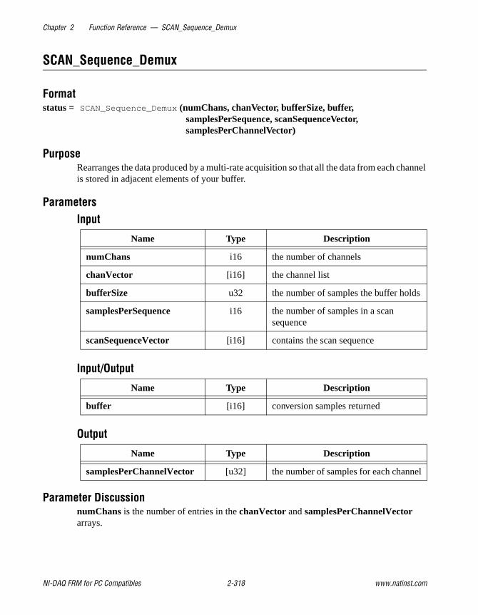
Chapter 2 Function Reference — SCAN_Sequence_Demux
NI-DAQ FRM for PC Compatibles 2-318 www.natinst.com
SCAN_Sequence_Demux
Formatstatus = SCAN_Sequence_Demux (numChans, chanVector, bufferSize, buffer,
samplesPerSequence, scanSequenceVector,samplesPerChannelVector)
PurposeRearranges the data produced by a multi-rate acquisition so that all the data from each channel is stored in adjacent elements of your buffer.
ParametersInput
Input/Output
Output
Parameter DiscussionnumChans is the number of entries in the chanVector and samplesPerChannelVector arrays.
Name Type Description
numChans i16 the number of channels
chanVector [i16] the channel list
bufferSize u32 the number of samples the buffer holds
samplesPerSequence i16 the number of samples in a scan sequence
scanSequenceVector [i16] contains the scan sequence
Name Type Description
buffer [i16] conversion samples returned
Name Type Description
samplesPerChannelVector [u32] the number of samples for each channel

Chapter 2 Function Reference — SCAN_Sequence_Demux
© National Instruments Corporation 2-319 NI-DAQ FRM for PC Compatibles
chanVector contains the channels sampled in the acquisition that produced the data contained in buffer. It might be identical to the channel vector you used in the call to SCAN_Sequence_Setup , or it might contain the channels in a different order. SCAN_Sequence_Demux will reorder the data in buffer such that the data for chanVector[0] occurs first, the data for chanVector[1] occurs second, and so on.
bufferSize is the number of samples in the buffer.
buffer is the array containing the data produced by the multi-rate acquisition. When SCAN_Sequence_Demux returns, the data in buffer will be rearranged.
samplesPerSequence is the number of samples in a scan sequence (obtained from a previous call to SCAN_Sequence_Setup ) and the size of the scanSequenceVector array.
scanSequenceVector contains the scan sequence created by NI-DAQ as a result of a previous call to SCAN_Sequence_Setup . You obtain a copy of scanSequenceVector by calling SCAN_Sequence_Retrieve .
samplesPerChannelVector contains the number of samples for each channel. The channel listed in entry i of chanVector will have a number of samples equal to the value of samplesPerChannelVector[i].
Using This FunctionSCAN_Sequence_Demux rearranges multirate data so that retrieving the data of a channel is more straightforward. The following example illustrates how to use this function:
The input parameters are as follows:numChans = 3chanVector = 2, 5, 7bufferSize = 14buffer = 2, 5, 7, 2, 2, 5, 2, 2, 5, 7, 2, 2, 5, 2 where a 2 represents a sample from
channel 2, and so on.samplesPerSequence = 7scanSequenceVector = 2, 5, 7, 2, 2, 5, 2
The output parameters are as follows:buffer = 2, 2, 2, 2, 2, 2, 2, 2, 5, 5, 5, 5, 7, 7 where a 2 represents a sample from
channel 2, and so on.samplesPerChannelVector = 8, 4, 2
The data from a channel can be located in the buffer by calculating the index of the first sample and the index of the last sample.
• The data from a channel listed in chanVect[0] (channel 2) begins at index 0 and ends at index samplesPerChannelVector [0] – 1 (index 7).

Chapter 2 Function Reference — SCAN_Sequence_Demux
NI-DAQ FRM for PC Compatibles 2-320 www.natinst.com
• The first sample for the channel listed in chanVector[1] (channel5) begins at samplesPerChannelVector [0] (index 8) and ends at (samplesPerChannelVector [0] + samplesPerChannelVector [1]) – 1 (index 11).
• The first sample for the channel listed inchanVector[2] (channel 7) begins at (samplesPerChannelVector [0] + samplesPerChannelVector [1]) (index 12) and ends at (samplesPerChannelVector [0] + samplesPerChannelVector [1] + samplesPerChannelVector [2]) – 1 (index 13).

Chapter 2 Function Reference — SCAN_Sequence_Retrieve
© National Instruments Corporation 2-321 NI-DAQ FRM for PC Compatibles
SCAN_Sequence_Retrieve
Formatstatus = SCAN_Sequence_Retrieve (deviceNumber, samplesPerSequence,
scanSequenceVector)
PurposeReturns the scan sequence created by NI-DAQ as a result of a previous call to SCAN_Sequence_Setup .
ParametersInput
Output
Parameter DiscussionsamplesPerSequence is the number of samples in a scan sequence (obtained from a previous call to SCAN_Sequence_Setup ) and the size of the scanSequenceVector output parameter.
scanSequenceVector contains the scan sequence created by NI-DAQ as a result of a previous call to SCAN_Sequence_Setup . The scan sequence will not contain the ghost channel place holders.
Using This FunctionSCAN_Sequence_Retrieve is used to obtain the actual scan sequence to program the device. You will need this information to call SCAN_Sequence_Demux to rearrange your data or to extract particular channels data from your acquisition buffer without rearranging it. If you use DAQ_Monitor to extract the data of a channel, you do not need the actual scan sequence.
Name Type Description
deviceNumber i16 assigned by configuration utility
samplesPerSequence i16 the number of samples in a scan sequence
Name Type Description
scanSequenceVector [i16] contains the scan sequence

Chapter 2 Function Reference — SCAN_Sequence_Setup
NI-DAQ FRM for PC Compatibles 2-322 www.natinst.com
SCAN_Sequence_Setup
Formatstatus = SCAN_Sequence_Setup (deviceNumber, numChans, chanVector, gainVector,
scanRateDivisorVector, scansPerSequence, samplesPerSequence)
PurposeInitializes the device for a multirate scanned data acquisition operation. Initialization includes selecting the channels to be scanned, assigning gains to these channels and assigning different sampling rates to each channel by dividing down the base scan rate.
ParametersInput
Output
Parameter DiscussionnumChans is the number of entries in the three input vectors. All three input vectors must have the same number of entries.
chanVector contains the onboard channels that will be scanned. A channel cannot be listed more the once. Refer to Appendix B, Analog Input Channel, Gain Settings, and Voltage Calculation, for valid channel settings.
Name Type Description
deviceNumber i16 assigned by configuration utility
numChans i16 number of channels
chanVector [i16] channel scan sequence
gainVector [i16] gain setting to be used for each channel in chanVector
scanRateDivisorVector [i16] rate divisor for each channel
Name Type Description
scansPerSequence i16 the number of scans in a scan sequence
samplesPerSequence i16 the number of samples in a scan sequence

Chapter 2 Function Reference — SCAN_Sequence_Setup
© National Instruments Corporation 2-323 NI-DAQ FRM for PC Compatibles
gainVector contains the gain settings to be used for each channel in chanVector. The channel listed in entry i of chanVector will list the gain in entry i of gainVector.
scanRateDivisorVector contains the scan rate divisors to be used for each channel. The sample rate for a channel equals the base scan rate (that is, the scan rate specified when SCAN_Start is called) divided by the scan rate divisor for that channel. The channel listed in entry i of chanVector will list the scan rate divisor in entry i of scanRateDivisorVector.
scansPerSequence is an output parameter that contains the total number of scans in the scan sequence created by NI-DAQ from your chanVector and scanRateDivisorVector including any scans that consist entirely of ghost channels, or place holders.
samplesPerSequence is an output parameter that contains the total number of samples in the scan sequence excluding any ghost channels. The total size of a scan sequence including ghost channels is limited by the size of the memory on your device used to hold this information. Currently, this limit is 512 entries. Because samplesPerSequence excludes ghost channels, an error might result even if samplesPerSequence is less than 512.
Using This FunctionThe following example shows how to use SCAN_Sequence_Setup :
numChans = 3chanVector = 2, 5, 7gainVector = 1, 1, 1scanRateDivisorVector = 1, 2, 4
The scan rate divisor for channel 2 is 1 so it is sampled at the base scan rate. The scan rate divisor for channel 5 is 2 so it is sampled at a rate equal to the base scan rate divided by 2. Likewise, the scan rate divisor for channel 7 is 4 so it is sampled at a rate equal to the base scan rate divided by 4.
The scan sequence created by NI-DAQ looks like this:
scan number: 1, 2, 3, 4channels sampled: 2, 5, 7, 2, 2, 5, 2scansPerSequence = 4 samplesPerSequence = 7
If your base scan rate is 1,000 scans/s, channel 2 is sampled at 1,000 S/s, channel 5 is sampled at 500 S/s, and channel 7 is sampled at 250 S/s.
scansPerSequence and samplesPerSequence are used to calculate the size of your acquisition buffer. Your buffer size must be an integer multiple of samplesPerSequence. Use scansPerSequence to size your buffer to hold some unit of time’s worth of data. For example,
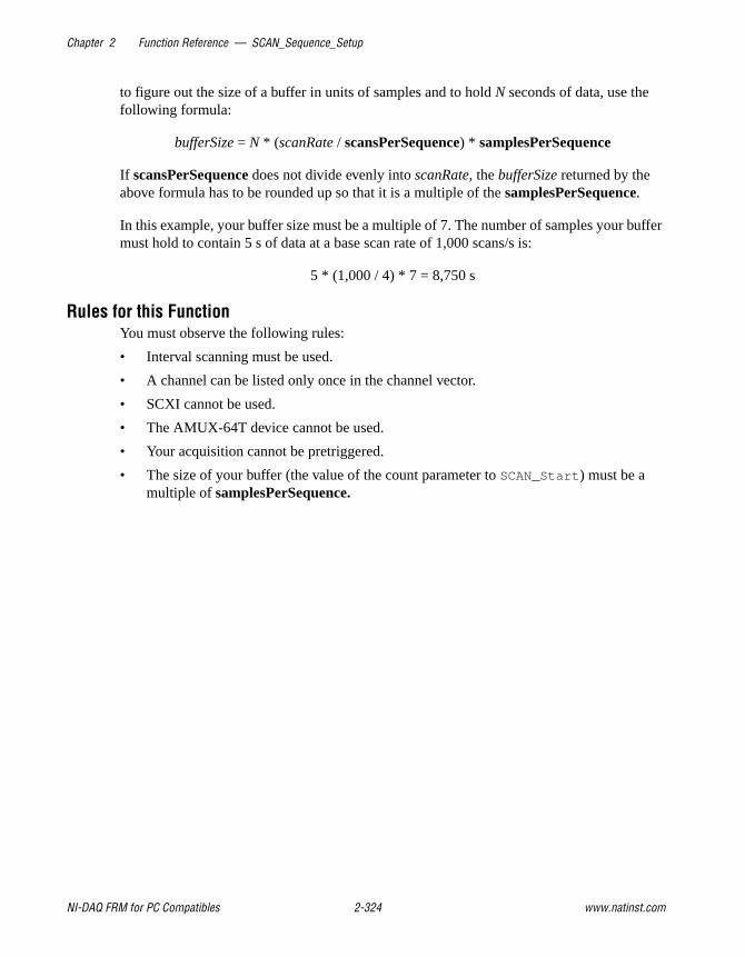
Chapter 2 Function Reference — SCAN_Sequence_Setup
NI-DAQ FRM for PC Compatibles 2-324 www.natinst.com
to figure out the size of a buffer in units of samples and to hold N seconds of data, use the following formula:
bufferSize = N * (scanRate / scansPerSequence) * samplesPerSequence
If scansPerSequence does not divide evenly into scanRate, the bufferSize returned by the above formula has to be rounded up so that it is a multiple of the samplesPerSequence.
In this example, your buffer size must be a multiple of 7. The number of samples your buffer must hold to contain 5 s of data at a base scan rate of 1,000 scans/s is:
5 * (1,000 / 4) * 7 = 8,750 s
Rules for this FunctionYou must observe the following rules:
• Interval scanning must be used.
• A channel can be listed only once in the channel vector.
• SCXI cannot be used.
• The AMUX-64T device cannot be used.
• Your acquisition cannot be pretriggered.
• The size of your buffer (the value of the count parameter to SCAN_Start ) must be a multiple of samplesPerSequence.

Chapter 2 Function Reference — SCAN_Setup
© National Instruments Corporation 2-325 NI-DAQ FRM for PC Compatibles
SCAN_Setup
Formatstatus = SCAN_Setup (deviceNumber, numChans, chanVector, gainVector)
PurposeInitializes circuitry for a scanned data acquisition operation. Initialization includes storing a table of the channel sequence and gain setting for each channel to be digitized (MIO and AI devices only).
ParametersInput
Parameter DiscussionnumChans is the number of channels in the chanVector.Range: 1 through 512 for the E Series devices.
1 through n for PCI-6110E, PCI-6111E, and DSA devices, where n is the number of physical channels onboard.1 through 256 when configuring scan for AI_Read_Scan or AI_VRead_Scan.
chanVector is an integer array of length numChans that contains the onboard channel scan sequence to be used. chanVector can contain any analog input channel number in any order. For the channel number range, refer to Table B-1, Valid Analog Input Channel Settings, in Appendix B, Analog Input Channel, Gain Settings, and Voltage Calculation. For example, if numChans = 4 and if chanVector[1] = 7, the second channel to be scanned is analog input channel 7, and four analog input channels are scanned.
Note The channels listed in the scan sequence refer to the onboard channel numbers.
Name Ty pe Description
deviceNumber i16 assigned by configuration utility
numChans i16 number of channels
chanVector [i16] channel scan sequence
gainVector [i16] gain setting to be used for each channel in chanVector

Chapter 2 Function Reference — SCAN_Setup
NI-DAQ FRM for PC Compatibles 2-326 www.natinst.com
If you use one or more external multiplexer devices (AMUX-64Ts) with any MIO or AI device except the MIO-64, the total number of channels scanned equals (4) * (numChans) * (number of AMUX-64T devices). For example, if you use one AMUX-64T and scan eight onboard channels, the total number of channels scanned equals (4) * (8) * (1) = 32.
If you use one or more external multiplexer devices (AMUX-64Ts) with the MIO-64, the total number of channels scanned equals (4) * (numChans1) * (num_mux_brds) + numChans2, where:
• 4 represents four-to-one multiplexer.
• numChans1 is the number of onboard channels (of an MIO or AI connector) scanned.
• Range: 0 through 7 differential, 0 through 15 single-ended.
• num_mux_brds is the number of external multiplexer devices.
• numChans2 is the number of onboard channels (of an analog connector, the second connector) scanned.
Range: 0 through 23 differential, 0 through 48 single-ended.
If you are using SCXI, you must scan the analog input channels on the DAQ device that corresponds to the SCXI channels you want. You should select the SCXI scan list using SCXI_SCAN_Setup before you call this function. Refer to the NI-DAQ User Manual for PC Compatibles for more information on SCXI channel assignments.
gainVector is an integer array of length numChans that contains the gain setting to be used for each channel specified in chanVector. This gain setting applies only to the DAQ device; if you use SCXI, you must establish any gain you want at the SCXI module either by setting jumpers on the module or by calling SCXI_Set_Gain . Refer to Appendix B, Analog Input Channel, Gain Settings, and Voltage Calculation, for valid gain settings.
For example, if gainVector[5] = 10, when NI-DAQ scans the sixth channel, the function sets the gain circuitry to a gain of 10. Notice also that gainVector[i] corresponds to chanVector[i]. If gainVector[2] = 100 and chanVector[2] = 3, the third channel NI-DAQ scans is analog input channel 3, and the function sets its gain to 100.
Note If you need to supply a gain of 0.5, use the value –1.
Using This FunctionSCAN_Setup stores numChans, chanVector, and gainVector in the Mux-Gain Memory table on the device. The function uses this memory table during scanning operations (SCAN_Start ) to automatically sequence through an arbitrary set of analog input channels and to allow gains to automatically change during scanning.

Chapter 2 Function Reference — SCAN_Setup
© National Instruments Corporation 2-327 NI-DAQ FRM for PC Compatibles
You need to call SCAN_Setup to set up a scan sequence for scanned operations; thereafter, you only need to call the function when you want a scan sequence. If you call DAQ_Start or AI_Read , NI-DAQ modifies the Mux-Gain Memory table on the device; therefore, you should use SCAN_Setup again after NI-DAQ modifies these calls to reinitialize the scan sequence.

Chapter 2 Function Reference — SCAN_Start
NI-DAQ FRM for PC Compatibles 2-328 www.natinst.com
SCAN_Start
Formatstatus = SCAN_Start (deviceNumber, buffer, count, sampTimebase, sampInterval,
scanTimebase, scanInterval)
PurposeInitiates a multiple-channel scanned data acquisition operation, with or without interval scanning, and stores its input in an array (MIO, AI, and DSA devices only).
ParametersInput
Input/Output
Parameter Discussionbuffer is an integer array. buffer must have a length equal to or greater than count.
Note For DSA devices, buffer should be an array of i32. These devices return the data in a 32-bit format in which the data bits are in the most significant bits.
Name Type Description
deviceNumber i16 assigned by configuration utility
count u32 number of samples
sampTimebase i16 resolution used for the sample-interval counter
sampInterval u16 length of the sample interval
scanTimebase i16 resolution for the scan-interval counter
scanInterval u16 length of the scan interval
Name Type Description
buffer [i16] used to hold acquired readings

Chapter 2 Function Reference — SCAN_Start
© National Instruments Corporation 2-329 NI-DAQ FRM for PC Compatibles
count is the number of samples to be acquired (that is, the number of A/D conversions to be performed). For double-buffered acquisitions, count specifies the size of the buffer, and count must be an even number.Range: 3 through 232 – 1 (except the E Series).
2 through 224 * (total number of channels scanned) or 232 – 1, whichever is less for E Series and DSA devices. For PCI-611X devices, count must be EVEN.
count must be an integer multiple of the total number of channels scanned. count refers to the total number of A/D conversions to be performed; therefore, the number of samples acquired from each channel is equal to count divided by the total number of channels scanned. This number is also the total number of scans. For the E Series devices, the total number of scans must be at least 2. If you do not use external multiplexer (AMUX-64T) devices, the total number of channels scanned is equal to the value of numChans (seeScan_Setup ).
If you use one or more external multiplexer devices with any MIO or AI device except the MIO-64, the total number of channels scanned equals (4) * (numChans) * (number of AMUX-64T devices). For example, if you use one AMUX-64T and scan eight onboard channels, the total number of channels scanned equals (4) * (8) * (1) = 32.
If you use one or more external multiplexer devices (AMUX-64Ts) with the MIO-64, the total number of channels scanned equals (4) * (numChans1) * (numMaxBrds) + numChans2, where:
• 4 represents a four-to-one multiplexer.
• numChans1 is the number of onboard channels (of an MIO or AI connector, the first connector) scanned.
Range: 0 through 7 differential, 0 through 15 single-ended.
• num_mux_brds is the number of external multiplexer devices.
• numChans2 is the number of onboard channels (of an analog connector, the second connector) scanned.
Range: 0 through 23 differential, 0 through 48 single-ended.
If you use SCXI, the total number of channels scanned is the total number of channels specified in the SCXI_SCAN_Setup call.
sampTimebase selects the clock frequency that indicates the timebase, or resolution, to be used for the sample-interval counter. The sample-interval counter controls the time that elapses between acquisition of samples within a scan sequence.
sampTimebase has the following possible values:–3: 20 MHz clock used as a timebase (50 ns resolution) (E Series only).–1: 5 MHz clock used as timebase (200 ns resolution).

Chapter 2 Function Reference — SCAN_Start
NI-DAQ FRM for PC Compatibles 2-330 www.natinst.com
0: External clock used as timebase (Connect your own timebase frequency to the internal scan-interval counter via the default PFI8 input for the E Series devices).
1: 1 MHz clock used as timebase (1 µs resolution).2: 100 kHz clock used as timebase (10 µs resolution).3: 10 kHz clock used as timebase (100 µs resolution).4: 1 kHz clock used as timebase (1 ms resolution).5: 100 Hz clock used as timebase (10 ms resolution).
On E Series devices, if you use this function with sampleTimebase set to 0 must call the Select_Signal function with signal set to ND_IN_CHANNEL_CLOCK_TIMEBASE and source set to a value other than ND_INTERNAL_20_MHZ and ND_INTERNAL_100_KHZ before calling SCAN_Start with sampleTimebase set to 0; otherwise, SCAN_Start selects low-to-high transitions on the PFI8 I/O connector pin as your external sample timebase.
If sample-interval timing is to be externally controlled (extConv = 1 or 3, see DAQ_Config ), NI-DAQ ignores the sampTimebase parameter, which can be any value.
On DSA devices, sampTimebase is ignored. Use DAQ_Set_Clock to set the can rate.
sampInterval indicates the length of the sample interval (that is, the amount of time to elapse between each A/D conversion within a scan sequence).Range: 2 through 65,535.
The sample interval is a function of the timebase resolution. The actual sample interval in seconds is determined by the following formula:
sampInterval * (sample timebase resolution)
where the sample timebase resolution equals one of the values of sampTimebase as specified above. For example, if sampInterval = 25 and sampTimebase = 2, the actual sample interval is 25 * 10 µs = 250 µs. The time to complete one scan sequence in seconds is (the actual sample interval) * (number of channels scanned). If the sample interval is to be externally controlled, the sampInterval parameter is ignored and can be any value.
On DSA devices, sampInterval is ignored. Use DAQ_Set_Clock to set the scan rate.
scanTimebase selects the clock frequency that indicates the timebase, or resolution, to be used for the scan-interval counter. The scan-interval counter controls the time that elapses between scan sequences. scanTimebase has the following possible values:
–3: 20 MHz clock used as a timebase (50 ns resolution) (E Series only).–1: 5 MHz clock used as timebase (200 ns resolution).0: External clock used as timebase (Connect your own timebase frequency to the
internal scan-interval counter via the default PFI8 input for the E Series devices).1: 1 MHz clock used as timebase (1 µs resolution).2: 100 kHz clock used as timebase (10 µs resolution).

Chapter 2 Function Reference — SCAN_Start
© National Instruments Corporation 2-331 NI-DAQ FRM for PC Compatibles
3: 10 kHz clock used as timebase (100 µs resolution).4: 1 kHz clock used as timebase (1 ms resolution).5: 100 Hz clock used as timebase (10 ms resolution).
On E Series devices, if you use this function with scanTimebase set to 0, you must call the function Select_Signal with signal set to ND_IN_SCAN_CLOCK_TIMEBASE and source set to a value other than ND_INTERNAL_20_MHZ and ND_INTERNAL_100_KHZ before calling SCAN_Start with scanTimebase set to 0; otherwise, SCAN_Start selects low-to-high transitions on the PFI8 I/O connector pin as your external scan timebase.
On DSA devices, scanTimebase is ignored. Use DAQ_Set_Clock to set the scan rate.
scanInterval indicates the length of the scan interval (that is, the amount of time that elapses between the initiation of each scan sequence). NI-DAQ scans all channels in the scan sequence at the beginning of each scan interval.Range: 0 or 2 through 65,535.
On DSA devices, scanInterval is ignored. Use DAQ_Set_Clock to set the scan rate.
If scanInterval equals 0, the time that elapses between A/D conversions and the time that elapses between scan sequences are both equal to the sample interval. That is, as soon as the scan sequence has completed, NI-DAQ restarts one sample interval later. Another advantage of setting scanInterval to 0 is that this frees the scan-interval counter (counter 2) for other operations such as waveform generation or general-purpose counting (non-E Series devices only).
The scan interval is a function of the scan timebase resolution. The actual scan interval in seconds is determined by the following formula:
scanInterval * (scan timebase resolution)
where the scan timebase resolution is equal to one of the values of scanTimebase as indicated above. For example, if scanInterval = 100 and scanTimebase = 2, the scan interval is 100 * 10 µs = 1 ms. This number must be greater than or equal to the sum of the total sample interval + 2 µs for most devices. If the scan interval is to be controlled by pulses applied to the OUT2 signal, NI-DAQ ignores this parameter (extConv = 2 or 3, see DAQ_Config ).
Note Simultaneous sampling devices ignore parameters for sampTimebase and sampInterval. These devices sample all channels simultaneously. The acquisition rate is controlled by scanTimebase and scanInterval; therefore, a scanInterval value of 0 is not allowed.

Chapter 2 Function Reference — SCAN_Start
NI-DAQ FRM for PC Compatibles 2-332 www.natinst.com
Using This FunctionSCAN_Start initializes the Mux-Gain Memory table to point to the start of the scan sequence as specified by SCAN_Setup. If you did not specify external sample-interval timing by the DAQ_Config call, NI-DAQ sets the sample-interval counter to the specified sampInterval and sampTimebase, sets the scan-interval counter to the specified scanInterval and scanTimebase, and sets up the sample counter to count the number of samples acquired and to stop the data acquisition process when the number of samples acquired equals count. If you have specified external sample-interval timing, the data acquisition circuitry relies on pulses received on the EXTCONV* input to initiate individual A/D conversions. In this case, NI-DAQ scans the channels repeatedly as fast as you apply the external conversion pulses.
SCAN_Start initializes a background data acquisition process to handle storing of A/D conversion samples into the buffer as NI-DAQ acquires them. When you use posttrigger mode (with pretrigger mode disabled), the process stores up to count A/D conversion samples into the buffer and ignores any subsequent conversions. NI-DAQ stores the acquired samples into the buffer with the channel scan sequence data interleaved; that is, the first sample is the conversion from the first channel, the second sample is the conversion from the second channel, and so on.
You cannot make the second call to SCAN_Start without terminating this background data acquisition process. If a call to DAQ_Check returns daqStopped = 1, the samples are available and NI-DAQ terminates the process. In addition, a call to DAQ_Clear terminates the background data acquisition process. Notice that if a call to DAQ_Check returns an error code of overFlowError or overRunError , or daqStopped = 1, the process is automatically terminated and there is no need to call DAQ_Clear .
If you enable pretrigger mode, SCAN_Start initiates a cyclical acquisition that continually fills the buffer with data, wrapping around to the start of the buffer once NI-DAQ has written to the entire buffer. When you apply the signal at the stop trigger input, SCAN_Start acquires an additional number of samples specified by the ptsAfterStoptrig parameter in DAQ_StopTrigger_Config and then terminates. Be aware that a scan sequence always completes. Therefore, NI-DAQ always obtains the most recent data point from the final channel in the scan sequence. When you enable pretrigger mode, the length of the buffer, which is greater than or equal to count, should be an integral multiple of numChans. If you observe this rule, a sample from the first channel in the scan sequence always resides at index = 0 in the buffer.
If you select external start triggering of the data acquisition operation, a transition on the line selected for the trigger initiates the data acquisition operation after the SCAN_Start call is complete. Otherwise, SCAN_Start issues a software trigger to initiate the data acquisition operation before returning.

Chapter 2 Function Reference — SCAN_Start
© National Instruments Corporation 2-333 NI-DAQ FRM for PC Compatibles
Note If your application calls DAQ_Start or SCAN_Start , always ensure that you call DAQ_Clear before your application terminates and returns control to the operating system. Unless you make this call (either directly, or indirectly through DAQ_Check or DAQ_DB_Transfer ), unpredictable behavior can result.
You must use the SCAN_Setup and SCAN_Start functions as a pair. Making a single call to SCAN_Setup with multiple calls to SCAN_Start fails and returns error noSetupError.
If you have an SC-2040 connected to your DAQ device, NI-DAQ ignores the sampTimebase and sampInterval parameters. NI-DAQ automatically supplies these parameters to optimally match your hardware.
If you select sampTimebase = 0 and scanTimebase = 0, you must use the same source for both. On E Series devices, if you use the Select_Signal function to specify the source of an external sample and external scan timebase, you must specify the same source for both timebases.

Chapter 2 Function Reference — SCAN_to_Disk
NI-DAQ FRM for PC Compatibles 2-334 www.natinst.com
SCAN_to_Disk
Formatstatus = SCAN_to_Disk (deviceNumber, numChans, chans, gains, filename, count, sampleRate,
scanRate, concat)
PurposePerforms a synchronous, multiple-channel scanned data acquisition operation and simultaneously saves the acquired data in a disk file. SCAN_to_Disk does not return until all the data has been acquired and saved or an acquisition error has occurred (MIO and AI devices only).
ParametersInput
Parameter DiscussionnumChans is the number of channels listed in chansArray.Range: 1 through 512 for the E Series devices.
1 through n for PCI-6110E, PCI-6111E, and DSA devices, where n is the number of physical channels onboard.
chans is an integer array of a length not less than numChans that contains the onboard channel scan sequence to be used. chans can contain any analog input channel number in any order. For channel number ranges, refer to Table B-1, Valid Analog Input Channel Settings,
Name Type Description
deviceNumber i16 assigned by configuration utility
numChans i16 number of channels
chans [i16] list of channels
gains [i16] list of gain settings
filename STR name of the data file
count u32 number of samples
sampleRate f64 desired sample rate in points per second
scanRate f64 desired scan rate in scans per second
concat i16 enables concatenation of existing file

Chapter 2 Function Reference — SCAN_to_Disk
© National Instruments Corporation 2-335 NI-DAQ FRM for PC Compatibles
in Appendix B, Analog Input Channel, Gain Settings, and Voltage Calculation. For example, if numChans = 4 and if chans[1] = 7, the second channel to be scanned is analog input channel 7, and NI-DAQ scans four analog input channels.
Note The channels contained in the chans array refer to the onboard channel numbers.
If you use one or more external multiplexer devices (AMUX-64Ts), with any MIO or AI device except the MIO-64, the total number of channels scanned equals (4) * (numChans) * (number of AMUX-64T devices). For example, if you use one AMUX-64T and scan eight onboard channels, the total number of channels scanned equals (4) * (8) * (1) = 32.
If you use one or more external multiplexer devices (AMUX-64Ts) with the MIO-64, the total number of channels scanned equals (4) * (numChans1) * (num_mux_brds) + numChans2, where:
• 4 represents a four-to-one multiplexer.
• numChans1 is the number of onboard channels (of an MIO or AI connector) scanned.
Range: 0 through 7 differential, 0 through 15 single-ended.
• num_mux_brds is the number of external multiplexer devices.
• numChans2 is the number of onboard channels (of an analog connector) scanned.
Range: 0 through 23 differential, 0 through 48 single-ended.
If you use SCXI, you must scan the analog input channels on the DAQ device that corresponds to the SCXI channels you want. You should select the SCXI scan list using SCXI_SCAN_Setup before you call this function. Refer to the NI-DAQ User Manual for PC Compatibles for more information on SCXI channel assignments.
gains is an integer array of a length not less than numChans that contains the gain setting to be used for each channel in the scan sequence selected in chans. NI-DAQ applies the gain value contained in gains[n] to the channel number contained in chans[n] when the function scans that channel. This gain setting applies only to the DAQ device; if you use SCXI, you must establish any gain you want at the SCXI module either by setting jumpers on the module or by calling SCXI_Set_Gain . Refer to Appendix B, Analog Input Channel, Gain Settings, and Voltage Calculation, for valid gain settings. If you use an invalid gain, NI-DAQ returns an error.
count is the number of samples to be acquired (that is, the number of A/D conversions to be performed). The length of your data file should be exactly twice the value of count. If you have previously enabled pretrigger mode (by a call to DAQ_StopTrigger_Config ), NI-DAQ ignores the count parameter.Range: 3 through 232 – 1 (except the E Series).
2 through 224 (E Series). For PCI-611X devices, count must be EVEN.

Chapter 2 Function Reference — SCAN_to_Disk
NI-DAQ FRM for PC Compatibles 2-336 www.natinst.com
sampleRate is the sample rate you want in units of points per second. This is the rate at which channels are sampled within a scan sequence.Range: Roughly 0.00153 pts/s through 1,000,000 pts/s.
scanRate is the scan rate you want in units of scans per second. This is the rate at which NI-DAQ performs scans. NI-DAQ performs a scan each time the function samples all the channels listed in the scan sequence.Range: 0 and roughly 0.00153 scans/s through 5,000,000 scans/s. A value of 0 means that
there is no delay between scans and that the effective scanRate is sampleRate/numChans.
concat enables concatenation of data to an existing file. Regardless of the value of concat, if the file does not exist, NI-DAQ creates the file.
0: Overwrite file if it exists.1: Concatenate new data to an existing file.
Using This FunctionSCAN_to_Disk initiates a synchronous process of acquiring A/D conversion samples and storing them in a disk file. Data is written to disk in a 16-bit binary format, with the lower byte first (little endian). The maximum rate varies according to the type of device you have and the speed and degree of fragmentation of your disk storage device. SCAN_to_Disk does not return control to your application until NI-DAQ acquires and saves all the samples you want (or until an acquisition error occurs). When you use posttrigger mode (with pretrigger mode disabled), the process stores count A/D conversions in the file and ignores any subsequent conversions.
Note If you have selected external start triggering of the data acquisition operation, a transition of an external signal initiates the data acquisition operation. If you are using all E Series devices, see the Select_Signal function for information about the external timing signals. Be aware that if you do not apply the start trigger, SCAN_to_Disk does not return control to your application. Otherwise, this function issues a software trigger to initiate the data acquisition operation.
If you have enabled pretrigger mode, the sample counter does not begin counting acquisitions until you apply a signal at the stop trigger input. Until you apply this signal, the acquisition continues to write data into the disk file. NI-DAQ ignores the value of the count parameter when you enable pretrigger mode. If you do not apply the stop trigger, SCAN_to_Disk eventually returns control to your application because you eventually run out of disk space.
In any case, you can use Timeout_Config to establish a maximum length of time for SCAN_to_Disk to execute.

Chapter 2 Function Reference — SCAN_to_Disk
© National Instruments Corporation 2-337 NI-DAQ FRM for PC Compatibles
Note Simultaneous sampling devices do not use the sampleRate parameter. Because these devices use simultaneous sampling of all channels the scanRate parameter controls the acquisition rate; therefore, a scanRate of 0 is not allowed.

Chapter 2 Function Reference — SCXI_AO_Write
NI-DAQ FRM for PC Compatibles 2-338 www.natinst.com
SCXI_AO_Write
Formatstatus = SCXI_AO_Write (SCXIchassisID, moduleSlot, channel, opCode, rangeCode,
voltCurrentData, binaryData, binaryWritten)
PurposeSets the DAC channel on the SCXI-1124 module to the specified voltage or current output value. You can also use this function to write a binary value directly to the DAC channel, or to translate a voltage or current value to the corresponding binary value.
ParametersInput
Output
Parameter Discussionchannel is the number of the analog output channels on the module.Range: 0 to 5.
opCode specifies the type of data to write to the DAC channel. You can also use opCode to tell SCXI_AO_Write to translate a voltage or current value and return the corresponding binary pattern in binaryWritten without writing anything to the module.
0: Write a voltage or current to channel.
Name Type Description
SCXIchassisID i16 chassis ID number
moduleSlot i16 module slot number
channel i16 the DAC channel of the module to write to
opCode i16 type of data
rangeCode i16 the voltage/current range to be used
voltCurrentData f64 voltage or current to be produced at the channel
binaryData i16 binary value to be written to the DAC
Name Type Description
binaryWritten i16 actual binary value written to the DAC

Chapter 2 Function Reference — SCXI_AO_Write
© National Instruments Corporation 2-339 NI-DAQ FRM for PC Compatibles
1: Write a binary value directly to channel.2: Translate a voltage or current value to binary, return in binaryWritten .
rangeCode is the voltage or current range to be used for the analog output channel.0: 0 to 1 V.1: 0 to 5 V.2: 0 to 10 V.3: –1 to 1 V.4: –5 to 5 V.5: –10 to 10 V.6: 0 to 20 mA.
voltCurrentData is the voltage or current you want to produce at the DAC channel output. If opCode = 1, NI-DAQ ignores this parameter. If opCode = 2, this is the voltage or current value you want to translate to binary. If the value is out of range for the given rangeCode, SCXI_AO_Write returns an error.
binaryData is the binary value you want to write directly to the DAC. If opCode is not 1, NI-DAQ ignores this parameter.Range: 0 to 4,095.
binaryWritten returns the actual binary value that NI-DAQ wrote to the DAC. SCXI_AO_Write uses a formula, given later in this section, using calibration constants that are stored on the module EEPROM to calculate the appropriate binary value that produces the given voltage or current. If opCode = 1, binaryWritten is equal to binaryData. If opCode= 2, SCXI_AO_Write calculates the binary value but does not write anything to the module.
Using This FunctionSCXI_AO_Write uses the following equation to translate voltage or current values to binary:
Bw = Bl + (Vw– Vl) * (Bh –Bl) / (Vh – Vl)
where
Bl = binary value that produces the low value of the rangeBh = binary value that produces the high value of the rangeVh = high value of the rangeVl = low value of the rangeVw = desired voltage or currentBw = the binary value which generates Vw
NI-DAQ loads a table of calibration constants from the SCXI-1124 EEPROM load area. The calibration table contains values for Bl and Bh for each channel and range.

Chapter 2 Function Reference — SCXI_AO_Write
NI-DAQ FRM for PC Compatibles 2-340 www.natinst.com
The SCXI-1124 is shipped with a set of factory calibration constants in the factory-set EEPROM area and a copy of the factory constants in the EEPROM load area. You can recalibrate your module and store your own calibration constants in the EEPROM load area using the SCXI_Cal_Constants function. Refer to the SCXI_Cal_Constants function description for calibration procedures and information about the module EEPROM.
If you want to write a binary value directly to the output channel, use opCode = 1. SCXI_AO_Write will not use the calibration constants or the conversion formula; it writes your binaryData value to the DAC.

Chapter 2 Function Reference — SCXI_Cal_Constants
© National Instruments Corporation 2-341 NI-DAQ FRM for PC Compatibles
SCXI_Cal_Constants
Formatstatus = SCXI_Cal_Constants (SCXIchassisID, moduleSlot, channel, opCode, calibrationArea,
rangeCode, SCXIgain, DAQboard, DAQchan, DAQgain,TBgain, scaled1, binary1, scaled2, binary2, calConst1, calConst2)
PurposeCalculates calibration constants for the given channel and range or gain using measured input value/binary pairs. You can use this with any SCXI analog input or analog output module. The constants can be stored and retrieved from NI-DAQ memory or the module EEPROM (if your module has an EEPROM). The driver uses the calibration constants to more accurately scale analog input data when you use the SCXI_Scale function and output data when you use SCXI_AO_Write .
ParametersInput
Name Type Description
SCXIchassisID i16 SCXI chassis ID number
moduleSlot i16 SCXI module slot number
channel i16 analog input or output channel number
opCode i16 operation to perform with the calibration constants
calibrationArea i16 where to store or retrieve constants
rangeCode i16 the voltage/current range for the analog output channel
SCXIgain f64 gain setting for the SCXI analog input channel
DAQboard i16 device number of DAQ device used to acquire binary1 and binary2
DAQchan i16 DAQ device channel number used when acquiring binary1 and binary2
DAQgain i16 DAQ device gain code used when acquiring binary1 and binary2

Chapter 2 Function Reference — SCXI_Cal_Constants
NI-DAQ FRM for PC Compatibles 2-342 www.natinst.com
Output
Parameter Discussionchannel is the number of the channel on the module.Range: 0 to n–1, where n is the number of channels available on the module.
–1: All channels on the module. For instance, the SCXI-1100, SCXI-1101, and SCXI-1122 modules have one amplifier for all channels, so calibration constants for those modules apply to all the module channels.
–2: The voltage (calConst2) and current excitation channels (calConst1) on the module. This is valid for the SCXI-1122 only, and only when opCode = 0.
opCode specifies the type of calibration operation to be performed.0: Retrieve calibration constants for the given channel and range or gain from
calibrationArea and return them in calConst1 and calConst2.1: Perform a one-point offset calibration calculation using (scaled1, binary1) for
the given channel and gain and write calibration constants to calibrationArea (analog input modules only).
2: Perform a two-point calibration calculation using (scaled1, binary1) and (scaled2, binary2) for the given channel and range or gain and write calibration constants to calibrationArea .
3: Write the calibration constants passed in calConst1 and calConst2 to calibrationArea for the given channel and range or gain.
4: Copy the entire calibration table in calibrationArea to the module EEPROM default load area so that it will be loaded automatically into NI-DAQ memory during subsequent application runs (SCXI-1101, SCXI-1102, SCXI-1104,
TBgain f64 SCXI terminal block gain, if any
scaled1 f64 voltage/current/frequency corresponding to binary1
binary1 f64 binary value corresponding to scaled1
scaled2 f64 voltage/current/frequency corresponding to binary2
binary2 f64 binary value corresponding to scaled2
Name Type Description
calConst1 *f64 return calibration constant
calConst2 *f64 return calibration constant
Name Type Description

Chapter 2 Function Reference — SCXI_Cal_Constants
© National Instruments Corporation 2-343 NI-DAQ FRM for PC Compatibles
SCXI-1122, SCXI-1124, SCXI-1126, SCXI-1141, SCXI-1142, and SCXI-1143 only).
5: Copy the entire calibration table in calibrationArea to driver memory so NI-DAQ can use the table in subsequent scaling operations in the current NI-DAQ session (SCXI-1122, SCXI-1124, SCXI-1126, SCXI-1141, SCXI-1142, and SCXI-1143 only).
calibrationArea is the location NI-DAQ uses for the calibration constants. Read the following Using This Function section for an explanation of the calibration table stored in NI-DAQ memory and the SCXI-1101, SCXI-1102, SCXI-1104, SCXI-1122, SCXI-1124, SCXI-1126, SCXI-1141, SCXI-1142, and SCXI-1143 EEPROM organization.
0: NI-DAQ memory. NI-DAQ maintains a calibration table in memory for use in scaling operations for the module.
1: Default EEPROM load area. NI-DAQ also updates the calibration table in memory when you write to the default load area (SCXI-1101, SCXI-1102, SCXI-1104, SCXI-1122, SCXI-1124, SCXI-1126, SCXI-1141, SCXI-1142, and SCXI-1143 only)
2: Factory-set EEPROM area. You cannot write to this area, but you can read or copy from it (SCXI-1101, SCXI-1102, SCXI-1104, SCXI-1122, SCXI-1124, SCXI-1126, SCXI-1141, SCXI-1142, and SCXI-1143 only).
3: User EEPROM area (SCXI-1101, SCXI-1102, SCXI-1104, SCXI-1122, SCXI-1124, SCXI-1126, SCXI-1141, SCXI-1142, and SCXI-1143 only).
rangeCode is the voltage or current range of the analog output channel. NI-DAQ only uses this parameter for analog output modules.
0: 0 to 1 V.1: 0 to 5 V.2: 0 to 10 V.3: –1 to 1 V.4: –5 to 5 V.5: –10 to 10 V.6: 0 to 20 mA.
SCXIgain is the SCXI module or channel gain/range setting. NI-DAQ only uses this parameter for analog input modules. Valid SCXIgain values depend on the module type:
SCXI-1100: 1, 2, 5, 10, 20, 50, 100, 200, 500, 1,000, 2,000SCXI-1101: 1SCXI-1102: 1, 100SCXI-1104: 0.1SCXI-1120: 1, 2, 5, 10, 20, 50, 100, 200, 250, 500, 1,000, 2,000SCXI-1120D: 0.5, 1, 2.5, 5, 10, 25, 50, 100, 250, 500, 1,000SCXI-1121: 1, 2, 5, 10, 20, 50, 100, 200, 250, 500, 1,000, 2,000SCXI-1122: 0.01, 0.02, 0.05, 0.1, 0.2, 0.5, 1, 2, 5, 10, 20, 50, 100, 200, 500, 1,000, 2,000SCXI-1126: 250, 500, 1,000, 2,000, 4,000, 8,000, 16,000, 32,000, 64,000, 128,000

Chapter 2 Function Reference — SCXI_Cal_Constants
NI-DAQ FRM for PC Compatibles 2-344 www.natinst.com
SCXI-1140: 1, 10, 100, 200, 500SCXI-1141: 1, 2, 5, 10, 20, 50, 100SCXI-1142: 1, 2, 5, 10, 20, 50, 100SCXI-1143: 1, 2, 5, 10, 20, 50, 100
DAQboard is the DAQ device you are using with this SCXI module. This applies only when opCode = 0, 1, 2, or 3 and moduleSlot is an analog input module. Otherwise, set to 0.
DAQchan is the analog input channel of DAQboard that you are using with this SCXI module. If you have only one chassis connected to DAQboard, and moduleSlot is in multiplexed mode, DAQchan should be 0. calConst1 is scaled by the current input range and polarity settings for this channel. This applies only when opCode = 0, 1, 2, or 3 and moduleSlot is an analog input module. Otherwise, set to 0.
DAQgain is the gain setting for DAQchan. It is used to scale calConst1 (binary offset). This applies only when opCode = 0, 1, 2, or 3 and moduleSlot is an analog input module. Otherwise, set to 0.
TBgain is the terminal block gain applied to the SCXI channel, if any. Currently, the SCXI-1327 terminal block is the only terminal block that applies gain to your SCXI channels. The SCXI-1327 has switches that you use to select either a gain of 1.0 or a gain of 0.01. You can use this terminal block with an SCXI-1120, SCXI-1120D, or SCXI-1121 module. For terminal blocks that do not apply gain to your SCXI channels, set TBgain =1.0.
scaled1, binary1 is the measured input value/binary pair you have taken for the given channel and range or gain. If the module is analog output, scaled1 is the voltage or current you measured at the output channel after writing the binary value binary1 to the output channel.
If the module is analog input, binary1 is the binary value you read from the input channel with a known voltage of scaled1 applied at the input. The binary1 parameter is a floating point, so you can take multiple binary readings from scaled1 and average them to be more accurate and reduce the effects of noise.
scaled2, binary2 is a second measured input value/binary pair you have taken for the given channel and range or gain. If the module is analog output, scaled2 is the voltage or current you measured when NI-DAQ wrote the binary value binary2 to the output channel. If the module is analog input, binary2 is the binary reading from the input channel with a known voltage of scaled2 applied at the input.
calConst1 is the first calibration constant. For analog output modules, calConst1 is the binary value that generates the voltage/current at the lower end of the voltage or current range. For analog input modules, calConst1 is the binary zero offset; that is, the binary reading that would result from an input value of zero. The offset is stored as a voltage and must be scaled to a binary value. It is scaled based on DAQgain and the current configuration of DAQchan (polarity and input range). If opCode= 1 or 2, calConst1 is a return value calculated from
Chapter 2 Function Reference — SCXI_Cal_Constants
© National Instruments Corporation 2-345 NI-DAQ FRM for PC Compatibles
the input value/binary pairs. If opCode = 0, calConst1 is a return constant retrieved from the calibrationArea . If opCode= 0 and channel = –2, calConst1 is the actual voltage excitation value returned in volts. If opCode = 3, you should pass your first calibration constant in calConst1 for NI-DAQ to store in calibrationArea .
calConst2 is the second calibration constant. For analog output modules, calConst2 is the binary value that generates the voltage/current at the upper end of the voltage/current range. For analog input modules, calConst2 is the gain adjust factor; that is, the ratio of the real gain to the ideal gain setting. If opCode = 1 or 2, calConst2 is a return value calculated from the input value/binary pairs. If opCode = 0, calConst2 is a return constant retrieved from the calibrationArea . If opCode= 0 and channel= –2, calConst2 is the actual current excitation value returned in units of milliamperes. If opCode = 3, you should pass your second calibration constant in calConst2 for NI-DAQ to store in calibrationArea .
Note C Programmers—calConst1 and calConst2 are pass-by-address parameters.
Using This FunctionAnalog Input CalibrationWhen you call SCXI_Scale to scale binary analog input data, NI-DAQ uses the binary offset and gain adjust calibration constants loaded for the given module, channel, and gain setting to scale the data to voltage or frequency. Refer to the SCXI_Scale function description for the equations used.
By default, NI-DAQ loads calibration constants for the SCXI-1101, SCXI-1102, SCXI-1104, SCXI-1122, SCXI-1126, SCXI-1141, SCXI-1142, and SCXI-1143 from the module EEPROM (see the EEPROM Organization section later in this function for more information). The SCXI-1141, SCXI-1142, and SCXI-1143 have only gain adjust constants in the EEPROM and do not have binary zero offset in the EEPROM. All other analog input modules have no calibration constants by default; NI-DAQ assumes no binary offset and ideal gain settings for those modules unless you use the following procedure to store calibration constants for your module.
You can determine calibration constants based specifically on your application setup, which includes your type of DAQ device, your DAQ device settings, and your cable assembly, all combined with your SCXI module and its configuration settings.
Note NI-DAQ stores constants in a table for each SCXI module gain setting. If your module has independent gains on each channel, NI-DAQ stores constants for each channel at each gain setting. When you use the following procedure, you are also calibrating for your DAQ device settings, so you must use the same DAQ device settings whenever you use the new calibration constants. The SCXI-1122, SCXI-1126, SCXI-1141, SCXI-1142, and SCXI-1143 factory-set EEPROM constants apply only to the SCXI-1122, SCXI-1126,

Chapter 2 Function Reference — SCXI_Cal_Constants
NI-DAQ FRM for PC Compatibles 2-346 www.natinst.com
SCXI-1141, SCXI-1142, and SCXI-1143 amplifiers, respectively, so you can use those with any DAQ device setup.
To perform a two-point analog input calibration, perform the following steps:
1. If you are using an E Series device, you should calibrate your ADC first using the Calibrate_E_Series function.
2. Make sure the SCXI gain is set to the gain you will be using in your application. If you are using an SCXI-1100, SCXI-1102, SCXI-1122, SCXI-1126, SCXI-1141, SCXI-1142, or SCXI-1143, you can use the SCXI_Set_Gain function, because those modules have software-programmable gain. For other analog input modules, you need to set gain jumpers or DIP switches appropriately.
3. Use SCXI_Single_Chan_Setup to program the module for a single-channel operation (as opposed to a channel scanning operation).
4. Ground your SCXI input channel. If you are using an SCXI-1100, SCXI-1101, SCXI-1122, SCXI-1141, SCXI-1142, or SCXI-1143, you can use the SCXI_Calibrate_Setup function to internally ground the module amplifier inputs. For other analog input modules, you need to wire the positive and negative channel inputs together at the terminal block.
5. Take several readings using the DAQ functions and average them for greater accuracy. You should use the DAQ device gain/range settings you will be using in your application. If you are using an E Series device, you may be able to enable dither using the MIO_Config function to make your averaging more accurate. You should average over an integral number of 60 Hz or 50 Hz power line cycles to eliminate line noise.
You now have your first input value/binary pair: scaled1 = 0.0, and binary1 is your binary reading or binary average.
6. Now apply a known, stable, non-zero input value to your input channel at the terminal block. Preferably, your input value should be close to the upper limit of your input range for the given gain setting.
7. Take another binary reading or average. If your binary reading is the maximum binary reading for your DAQ device, you should try a smaller input value. This is your second input value/binary pair: scaled2 and binary2.
8. Call SCXI_Cal_Constants with your two input value/binary pairs and opCode = 2. Make sure you pass the correct SCXIgain you used and pass the gain code you used in AI_Read or DAQ_Op in the DAQgain parameter.
If you are using an SCXI-1101, SCXI-1102, SCXI-1104, SCXI-1122, SCXI-1126, SCXI-1141, SCXI-1142, or SCXI-1143, you can save the constants in the module EEPROM (calibrationArea = 1 or 3). Refer to the EEPROM Organization section later in this function for information about constants in the EEPROM. It is best to use calibrationArea = 3 (user EEPROM area) as you are calibrating, and then call SCXI_Cal_Constants again at the end of your calibration sequence with opCode = 4

Chapter 2 Function Reference — SCXI_Cal_Constants
© National Instruments Corporation 2-347 NI-DAQ FRM for PC Compatibles
to copy your EEPROM area to the default EEPROM load area. That way there are two copies of your new constants, and you can revert to the factory constants using opCode = 4 without wiping out your new constants entirely.
For other analog input modules, you must specify calibrationArea = 0 (NI-DAQ memory). Unfortunately, calibration constants stored in NI-DAQ memory are lost at the end of the current NI-DAQ session. You might want to create a file and save the constants returned in calConst1 and calConst2 so that you can load them again in subsequent application runs using SCXI_Cal_Constants with opCode = 3.
Any subsequent calls to SCXI_Scale for the given module, channel, and gain setting will use the new calibration constants when scaling. You can repeat steps 2 through 8 for any other channel or gain settings you want to calibrate.
You can use a different input value for the first measurement instead of grounding the input channel. For instance, if you know you will be using a specific input value range, you might use the endpoints of your expected input range as scaled1 and scaled2. Then you would be specifically calibrating your expected input range.
If you are using an SCXI-1100, SCXI-1101, SCXI-1122, SCXI-1126, SCXI-1141, SCXI-1142, or SCXI-1143, you can perform a one-point calibration to determine the binary offset; you can do this easily without external hookups using the SCXI_Calibrate_Setup function to internally ground the amplifier. Use the procedure above, skipping steps 6 and 7, and using opCode = 1 for the SCXI_Cal_Constants function.
If you are storing calibration constants in the SCXI-1101, SCXI-1102, SCXI-1104, SCXI-1122, SCXI-1126,SCXI-1141, SCXI-1142, or SCXI-1143 EEPROM, your binary offset and gain adjust factors must not exceed the ranges given in the respective module user manuals. The constant format in the EEPROM does not allow for larger constants. If your constants exceed these specifications, the function returns badExtRefError . If this error occurs, you should make sure your SCXIgain, DAQgain, and TBgain values are the actual settings you used to measure the volt/binary pairs, and you might want to recalibrate your DAQ device, if applicable.
Analog Output CalibrationWhen you call SCXI_AO_Write to output a voltage or current to your SCXI-1124 module, NI-DAQ uses the calibration constants loaded for the given module, channel, and output range to scale the voltage or current value to the appropriate binary value to write to the output channel. By default, NI-DAQ loads calibration constants into memory for the SCXI-1124 from the module EEPROM load area (see the EEPROM Organization section for more information).

Chapter 2 Function Reference — SCXI_Cal_Constants
NI-DAQ FRM for PC Compatibles 2-348 www.natinst.com
You can recalibrate your SCXI-1124 module to create your own calibration constants using the following procedure:
1. Use the SCXI_AO_Write function with opCode = 1. If you are calibrating a voltage output range, pass the parameter binaryData = 0. If you are calibrating the 0 to 20 mA current output range (rangeCode = 6), pass the parameter binaryData = 255.
2. Measure the output voltage or current at the output channel with a voltmeter. This is your first volt/binary pair: binary1 = 0 or 255 and scaled1 is the voltage or current you measured at the output.
3. Use the SCXI_AO_Write function with opCode = 1 to write the binaryData = 4,095 to the output DAC.
4. Measure the output voltage or current at the output channel. This is your second volt/binary pair: binary2 = 4,095 and scaled2 is the voltage or current you measured at the output.
5. Call SCXI_Cal_Constants with your input value/binary pairs and opCode = 2. You can save the constants on the module EEPROM (calibrationArea = 1 or 3). Refer to the following EEPROM Organization section for information about constants in the EEPROM. It is best to use calibrationArea = 3 (user EEPROM area) as you are calibrating, and then call SCXI_Cal_Constants again at the end of your calibration sequence with opCode = 4 to copy the user EEPROM area to the default load area. That way there will be two copies of your new constants and you can revert to the factory constants using opCode = 4 without wiping out your new constants entirely.
Repeat the procedure above for each channel and range you want to calibrate. Subsequent calls to SCXI_AO_Write will use your new constants to scale voltage or current to the correct binary value.
EEPROM OrganizationThe SCXI-1101, SCXI-1102, SCXI-1104, SCXI-1122, SCXI-1124, SCXI-1126, SCXI-1141, SCXI-1142, and SCXI-1143 modules have an onboard EEPROM to handle storage of calibration constants. The EEPROM is divided into the following three areas:
• The factory area is shipped with a set of factory calibration constants; you cannot write into the factory area, but you can read from it.
• The default load area is where NI-DAQ automatically looks to load calibration constants the first time you access the module during an NI-DAQ session using an NI-DAQ function call, such as SCXI_Reset , SCXI_Single_Chan_Setup , or SCXI_AO_Write . When the module is shipped, the default load area contains a copy of the factory calibration constants. When you write to the default load area using SCXI_Cal_Constants , NI-DAQ also updates the constants in NI-DAQ memory.

Chapter 2 Function Reference — SCXI_Cal_Constants
© National Instruments Corporation 2-349 NI-DAQ FRM for PC Compatibles
• The user area is an area for you to store your own calibration constants that you calculate by following the instructions above and using the SCXI_Cal_Constants function. You can also put a copy of your own constants in the default load area if you want NI-DAQ to automatically load your constants for subsequent NI-DAQ sessions.

Chapter 2 Function Reference — SCXI_Calibrate
NI-DAQ FRM for PC Compatibles 2-350 www.natinst.com
SCXI_Calibrate
Formatstatus = SCXI_Calibrate (SCXIchassisID, moduleSlot, moduleChan, opCode, calibrationArea,
SCXIgain, refVoltage, DAQdevice, DAQchan)
PurposePerforms either a two-point offset/gain-adjust calibration (for the SCXI-1112 module) or a one-point offset calibration (for the SCXI-1125 module). The calculated offset/gain-adjust calibration constants are then stored in the default EEPROM load area, as well as in current NI-DAQ memory. Two-point calibrations use an internal reference voltage. The actual value of the voltage reference is stored in the module EEPROM. This function allows the updating of the reference voltage value in the EEPROM to correct for drift over time. This function also allows calibration constants from other EEPROM areas (user and factory) or NI-DAQ memory to be copied to the default EEPROM load area.
Note The module has to be in multiplexed mode in order to use this function.
ParametersInput
Name Type Description
SCXIChassisID i16 SCXI chassis ID number
moduleSlot i16 SCXI module slot number
moduleChan i16 module input channel number
opCode i16 operation to perform
calibrationArea i16 location of the calibration constants that are copied when performing a copy-to-load-area operation
SCXIgain f64 gain setting for the SCXI input channel to be calibrated
refVoltage f64 value of reference voltage to be stored in the EEPROM for the external calibration operation

Chapter 2 Function Reference — SCXI_Calibrate
© National Instruments Corporation 2-351 NI-DAQ FRM for PC Compatibles
Parameter DiscussionmoduleChan is the number of the channel on the module.Range: 0 to n-1, where n is the number of channels available on the module.
opCode specifies the particular operation to perform.0: Perform a two-point calibration (for the SCXI-1112) or a one-point calibration
(for the SCXI-1125) for the given channel and gain and write the calculated calibration constants to the default EEPROM load area of the module, as well as to current NI-DAQ memory.
1: (SCXI-1112 only)—Take the value passed in the refVoltage parameter and write it to the module EEPROM in the area used to store the internal reference voltage.
2: Copy the calibration constants in the area specified by calibrationArea to the default EEPROM load area.
calibrationArea is the location NI-DAQ uses for the calibration constants. 0: NI-DAQ memory—NI-DAQ maintains a calibration table in memory for use in
scaling operations for the module.1: Default EEPROM load area.2: Factory EEPROM area—You cannot write to this area, but you can read or copy
from it.3: (not on the SCXI-1125)—User EEPROM area.
SCXIgain is the SCXI channel gain setting. Valid SCXIgain values depend on the module type.
SCXI-1112:100SCXI-1125:1, 2, 5, 10, 20, 50, 100, 200, 250, 500, 1,000, 2,000
(SCXI-1112 only)—refVoltage is the voltage value to store in the module EEPROM area reserved for the value of the onboard voltage reference used to perform a two-point calibration. This applies only when opCode = 1. Otherwise, set refVoltage to 0.0.
DAQdevice is the DAQ device you are using with this SCXI module. This is used only for opCode = 0. Otherwise, set DAQdevice to 0.
DAQdevice i16 device number of DAQ device you use to acquire data from the module that you calibrate
DAQchan i16 DAQ device channel you use to acquire data from the module being calibrated
Name Type Description

Chapter 2 Function Reference — SCXI_Calibrate
NI-DAQ FRM for PC Compatibles 2-352 www.natinst.com
DAQchan is the analog input channel of DAQdevice that you are using with this SCXI module. In most cases this will be channel 0. This applies only when opCode = 0. Otherwise, set DAQdevice to 0.
Using This FunctionWhen you call SCXI_Scale to scale binary analog input data, NI-DAQ uses the binary offset and gain adjust calibration constants loaded for the given module, channel, and gain setting to scale the data to voltage. Please refer to the SCXI_Scale function description for the equations used.
By default, NI-DAQ loads calibration constants from the module EEPROM for modules that store calibration constants in an EEPROM. The modules that this function supports, the SCXI-1112 and the SCXI-1125, both have EEPROMs with calibration constants. See the EEPROM Organization section later in this function for more information.
To calibrate the SCXI-1112 (a two-point offset and gain adjust calibration) or the SCXI-1125 (just a one-point offset calibration), perform the following steps:
1. Calibrate the DAQ device you will be using. For an E Series device, use the Calibrate_E_Series function.
2. Make sure the module is configured to be in multiplexed mode.
3. Call SCXI_Calibrate with opCode = 0 and the other parameters set up appropriately as described in this function description.
Any subsequent calls to SCXI_Scale for the given module, channel, and gain setting use the new calibration constants when scaling. You can repeat step 3 for any other channel or gain settings you want to calibrate.
In performing a calibration operation on the SCXI-1112, SCXI_Calibrate routes an onboard reference voltage to the channel you calibrate. The value of this reference voltage is read from the module EEPROM. Over time and depending on the conditions the system is set in, the reference voltage value may drift. When this happens, you need to update the reference voltage value stored in the EEPROM. To do this, perform the following steps:
1. Use SCXI_Calibrate_Setup with operation = 3 to route the module onboard reference directly to the module output.
2. Use a DMM to accurately measure the value of the reference.
3. Call SCXI_Calibrate with opCode = 1 and refVoltage set to the value measured in step 2.

Chapter 2 Function Reference — SCXI_Calibrate
© National Instruments Corporation 2-353 NI-DAQ FRM for PC Compatibles
EEPROM OrganizationThe modules supported by SCXI_Calibrate , the SCXI-1112 and the SCXI-1125, have onboard EEPROMs to handle storage of calibration constants. In the case of the SCXI-1112, the onboard reference voltage value is stored in its own area, independent of the area containing calibration constants. The EEPROM is divided into either three areas, in the case of the SCXI-1112, or two areas in the case of the SCXI-1125:
• The factory area is shipped with a set of factory calibration constants; you cannot write into the factory area, but you can read from it.
• The default load area is where NI-DAQ automatically looks to load calibration constants the first time they are accessed. When the module is shipped, the default load area contains a copy of the factory calibration constants. When you write to the default load area using SCXI_Calibrate with opCode = 0, NI-DAQ also updates the constants in NI-DAQ memory.
• The user area, which is not present on the SCXI-1125, is the area where you store your own calibration constants. Please refer to the SCXI_Cal_Constants function description for more information about this area.
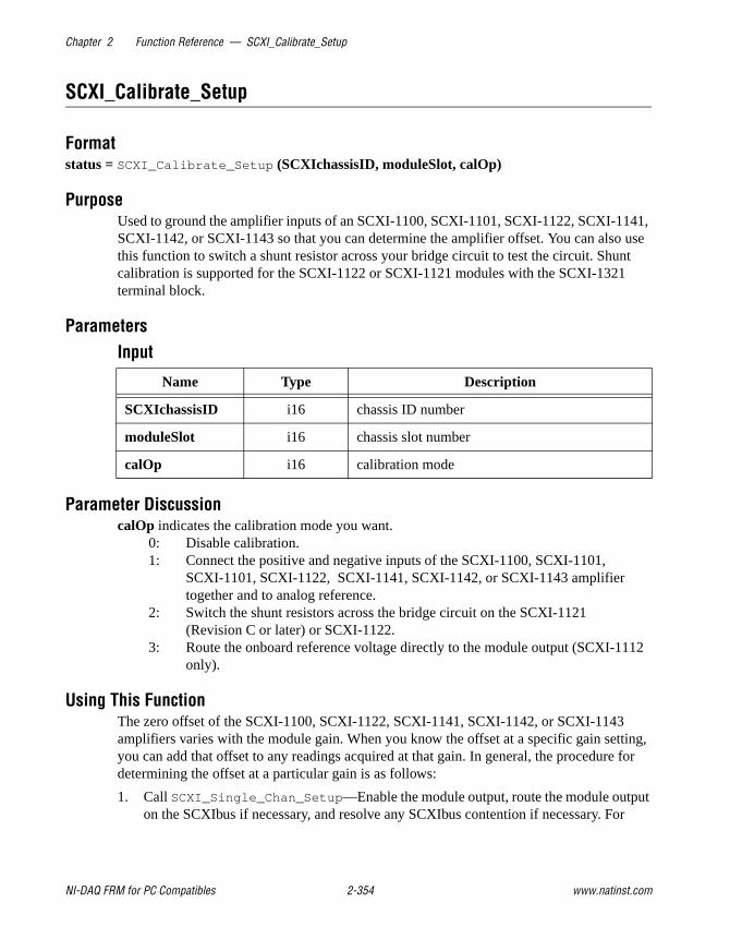
Chapter 2 Function Reference — SCXI_Calibrate_Setup
NI-DAQ FRM for PC Compatibles 2-354 www.natinst.com
SCXI_Calibrate_Setup
Formatstatus = SCXI_Calibrate_Setup (SCXIchassisID, moduleSlot, calOp)
PurposeUsed to ground the amplifier inputs of an SCXI-1100, SCXI-1101, SCXI-1122, SCXI-1141, SCXI-1142, or SCXI-1143 so that you can determine the amplifier offset. You can also use this function to switch a shunt resistor across your bridge circuit to test the circuit. Shunt calibration is supported for the SCXI-1122 or SCXI-1121 modules with the SCXI-1321 terminal block.
ParametersInput
Parameter DiscussioncalOp indicates the calibration mode you want.
0: Disable calibration.1: Connect the positive and negative inputs of the SCXI-1100, SCXI-1101,
SCXI-1101, SCXI-1122, SCXI-1141, SCXI-1142, or SCXI-1143 amplifier together and to analog reference.
2: Switch the shunt resistors across the bridge circuit on the SCXI-1121 (Revision C or later) or SCXI-1122.
3: Route the onboard reference voltage directly to the module output (SCXI-1112 only).
Using This FunctionThe zero offset of the SCXI-1100, SCXI-1122, SCXI-1141, SCXI-1142, or SCXI-1143 amplifiers varies with the module gain. When you know the offset at a specific gain setting, you can add that offset to any readings acquired at that gain. In general, the procedure for determining the offset at a particular gain is as follows:
1. Call SCXI_Single_Chan_Setup —Enable the module output, route the module output on the SCXIbus if necessary, and resolve any SCXIbus contention if necessary. For
Name Type Description
SCXIchassisID i16 chassis ID number
moduleSlot i16 chassis slot number
calOp i16 calibration mode

Chapter 2 Function Reference — SCXI_Calibrate_Setup
© National Instruments Corporation 2-355 NI-DAQ FRM for PC Compatibles
the SCXI-1100, SCXI-1101, and SCXI-1122, the module channel you specify is irrelevant.
2. Call SCXI_Set_Gain —Set the module gain to the setting that you will use in your application.
3. Call SCXI_Calibrate_Setup —Ground the amplifier inputs.
4. Acquire data using the DAQ functions—you should acquire and average many samples. If you have enabled the filter on the module, wait for the amplifier to settle after calling SCXI_Calibrate_Setup before you acquire data. Refer to your SCXI-1100, SCXI-1122, SCXI-1141, SCXI-1142, or SCXI-1143 user manuals for settling times caused by filter settings.
5. Call SCXI_Calibrate_Setup —Disable calibration.
6. Continue with your application—Whenever you acquire samples from the module at the gain that you chose in step 2, subtract the binary offset that you read in step 4 from each sample before scaling the data, or call SCXI_Cal_Constants to store the offset in NI-DAQ memory or the EEPROM. Then, subsequent calls to SCXI_Scale for the given gain automatically subtracts the offset for you. Refer to the SCXI_Cal_Constants function for more information.
Refer to your SCXI-1122 or SCXI-1321 user manuals for information about how the module applies the shunt resistor when calOp = 2.
The SCXI-1141, SCXI-1142, and SCXI-1143 have a separate amplifier for each channel, so you have to repeat the above procedure for each channel you want to calibrate.

Chapter 2 Function Reference — SCXI_Change_Chan
NI-DAQ FRM for PC Compatibles 2-356 www.natinst.com
SCXI_Change_Chan
Formatstatus = SCXI_Change_Chan (SCXIchassisID, moduleSlot, moduleChan)
PurposeSelects a new channel of a multiplexed module that you have previously set up for a single-channel analog input operation using the SCXI_Single_Chan_Setup function.
ParametersInput
Parameter DiscussionmoduleChan is the channel number of the new input channel on the module that is to be read.Range: 0 to n–1, where n is the number of input channels on the module.
–1: Set up to read the temperature sensor on the terminal block connected to the module if the temperature sensor is in the MTEMP configuration.
(SCXI-1112 only) c = –1 to (–n), where n is the number of analog input channels on the module. This number selects the CJTEMP channel on the analog input channel (–c) –1; that is, –1 selects the CJTEMP channel on channel 0, –2 selects the CJTEMP channel on channel 1, and so on.
Using This FunctionIt is important to realize that this function affects only the channel selection on the module. It does not affect the module output enable or any analog signal routing on the SCXIbus; theSCXI_Single_Chan_Setup function is required to do that. SCXI_Change_Chan can be very useful in applications like those shown in Chapter 3, Software Overview, of the NI-DAQ User Manual for PC Compatibles, especially when you are trying to read several channels on a module in a loop at relatively high speeds. However, you will need to call SCXI_Single_Chan_Setup again to select a channel on a different module.
Name Type Description
SCXIchassisID i16 chassis ID number
moduleSlot i16 chassis slot number
moduleChan i16 channel number

Chapter 2 Function Reference — SCXI_Configure_Filter
© National Instruments Corporation 2-357 NI-DAQ FRM for PC Compatibles
SCXI_Configure_Filter
Formatstatus = SCXI_Configure_Filter (SCXIchassisID, moduleSlot, channel, filterMode, freq,
cutoffDivDown, outClkDivDown, actualFreq)
PurposeConfigures the filter on any SCXI module that supports programmable filter settings. Currently, only the SCXI-1122, SCXI-1125, SCXI-1126, SCXI-1141, SCXI-1142, and SCXI-1143 have programmable filter settings; the other analog input modules have hardware-selectable filters.
ParametersInput
Output
Parameter Discussionchannel is the module channel for which you want to change the filter configuration. If channel = –1, SCXI_Configure_Filter changes the filter configuration for all channels on the module.
filterMode indicates the filter configuration mode for the given channel.0: Bypass the filter.1: Set filter cutoff frequency to freq.
Name Type Description
SCXIchassisID i16 chassis ID number
moduleSlot i16 chassis slot number
channel i16 module channel
filterMode i16 filter configuration mode
freq f64 filter cutoff frequency
cutoffDivDown u16 external signal divisor for cutoff frequency
outClkDivDown u16 clock signal divisor to send to OUTCLK
Name Type Description
actualFreq f64 actual filter cutoff frequency

Chapter 2 Function Reference — SCXI_Configure_Filter
NI-DAQ FRM for PC Compatibles 2-358 www.natinst.com
2: Configure the filter to use an external signal. The module divides the external signal by cutoffDivDown to determine the filter cutoff frequency. The module also divides the external signal by outClkDivDown and sends it to the module front connector OUTCLK pin. You can use this filter mode to configure a tracking filter. You can use this mode only with the SCXI-1141, SCXI-1142, and SCXI-1143.
3: Enable the filter (the reverse of filterMode 0).
freq is the cutoff frequency you want to select from the frequencies available on the module if filterMode = 1.
The SCXI-1122 has two possible cutoff frequencies:
4.0: –10 dB at 4 Hz
4,000.0: –3 dB at 4 kHz
The SCXI-1125 has two possible cutoff frequencies:
4.0: –10 dB at 4 Hz
10,000: –3 dB at 10 kHz
The SCXI-1126 has four possible cutoff frequencies (1 Hz, 40 Hz, 320 Hz, and 1 kHz), which attenuate at –80 dB.
The SCXI-1141, SCXI-1142, and SCXI-1143 have a range of cutoff frequencies from 10 Hz to 25 kHz. SCXI_Configure_Filter produces the frequency you want as closely as possible by dividing an internal 10 MHz signal on the SCXI-1141, SCXI-1142, or SCXI-1143. The function returns the exact cutoff frequency produced in the output parameter actualFreq.
If filterMode = 2, set freq to the approximate frequency of the external signal you are using. Refer to the user manual for your SCXI-1141, SCXI-1142, or SCXI-1143 module for an explanation of the impact of different signal frequencies on the filters.
If filterMode = 0 or 3, NI-DAQ ignores freq.
cutoffDivDown is an integer by which the module divides the external signal to determine the filter cutoff frequency when filterMode = 2. NI-DAQ ignores this parameter if filterMode is not 2.Range: 2 to 65,535.
outClkDivDown is an integer by which the module divides either the internal 10 MHz signal (if filterMode = 1) or the external signal (if filterMode = 2) to send back to the module front connector OUTCLK pin. This parameter is only used for the SCXI-1141, SCXI-1142, and SCXI-1143. Range: 2 to 65,535.

Chapter 2 Function Reference — SCXI_Configure_Filter
© National Instruments Corporation 2-359 NI-DAQ FRM for PC Compatibles
actualFreq returns the actual cutoff frequency that the module uses.
Using this FunctionThe SCXI-1122 has one filter setting applied to all channels on the module; therefore, you must set channel = –1. The SCXI-1122 and the SCXI-1125 only work with filterMode = 1; you cannot configure the SCXI-1122 or the SCXI-1125 to bypass the filter or to use an external signal to set the cutoff frequency. The default frequency setting for the SCXI-1122 and the SCXI-1125 is 4 Hz.
The SCXI-1126 has eight filter settings, one for each channel. These settings only work with filterMode = 1. The default frequency setting for the SCXI-1126 is 1 Hz.
The SCXI-1141, SCXI-1142, and SCXI-1143 also have one filter setting applied to all channels, so you must use channel= –1 when you select a cutoff frequency for your module. After you select the cutoff frequency for the entire module, you can configure one or more of the channels to enable the filter by calling SCXI_Configure_Filter again for each channel and setting filterMode = 3. By default, all the channel filters on the SCXI-1141, SCXI-1142, and SCXI-1143 are bypassed.

Chapter 2 Function Reference — SCXI_Get_Chassis_Info
NI-DAQ FRM for PC Compatibles 2-360 www.natinst.com
SCXI_Get_Chassis_Info
Formatstatus = SCXI_Get_Chassis_Info (SCXIchassisID, chassisType, chassisAddress, commMode,
commPath, numSlots)
PurposeReturns chassis configuration information.
ParametersInput
Output
Parameter DiscussionchassisType indicates what type of SCXI chassis is configured for the given SCXIchassisID.
0: SCXI-1000 4-slot chassis.1: SCXI-1001 12-slot chassis.2: SCXI-2000 4-slot remote chassis.3: VXI-SC-1000 carrier module.4: PXI-1010 chassis.5: PXI-1011 chassis.
chassisAddress is the hardware-jumpered address of an SCXI chassis.Range: 0 to 31 (SCXI-1000, SCXI-1001, VXI-SC-1000, and PXI-1010).
0 to 255 (SCXI-2000 or SCXI chassis with SCXI-2400 module).
Name Type Description
SCXIchassisID i16 chassis ID number
Name Type Description
chassisType *i16 type of SCXI chassis
chassisAddress *i16 hardware jumpered address of an SCXI-1001 chassis
commMode *i16 communication mode
commPath *i16 communication path
numSlots *i16 number of plug-in module slots
Chapter 2 Function Reference — SCXI_Get_Chassis_Info
© National Instruments Corporation 2-361 NI-DAQ FRM for PC Compatibles
commMode is the Communication mode that is used when the driver communicates with the SCXI chassis and modules.
0: Communication mode is disabled. In effect, the chassis is disabled.1: Serial communication is enabled through a digital port of a DAQ device that is
cabled to a module in the chassis.2: Serial communication is enabled over the PC parallel port that is cabled to the
SCXI-1200 module.3: Serial communication is enabled over the PC serial port that is cabled to one or
more SCXI-2000 chassis or SCXI-2400 modules.4: Serial communication is enabled over the VXI backplane.5: Serial communication is enabled through a digital port of a DAQ device internally
connected to the SCXIbus of a PXI-1010 or PXI-1011 chassis.
commPath is the communication path that is used when the driver communicates with the SCXI chassis and modules. If commMode = 1, 2, 4, or 5, commPath should be the device number of the DAQ device that is the designated communicator for the chassis. If commMode = 3, commPath is the serial port for this chassis. When commMode = 0, commPath is meaningless.
numSlots is the number of plug-in module slots in the SCXI chassis.4: For the SCXI-1000, SCXI-2000, and PXI-1010 chassis.8: For the PXI-1011 chassis.
12: For the SCXI-1001 chassis.24: For the VXI-SC-1000 carrier module.
Note C Programmers—chassisType, chassisAddress, commMode, commPath, and numSlots are pass-by-address parameters.

Chapter 2 Function Reference — SCXI_Get_Module_Info
NI-DAQ FRM for PC Compatibles 2-362 www.natinst.com
SCXI_Get_Module_Info
Formatstatus = SCXI_Get_Module_Info (SCXIchassisID, moduleSlot, modulePresent, operatingMode,
DAQdeviceNumber)
PurposeReturns configuration information for the given chassis slot number.
ParametersInput
Output
Parameter DiscussionmodulePresent indicates what type of module is present in the given slot.
–1: Empty slot; there is no module present in the given slot.1: SCXI-1126.2: SCXI-1121.4: SCXI-1120.6: SCXI-1100.8: SCXI-1140.
10: SCXI-1122.12: SCXI-1160.13: SCXI:1125.14: SCXI-1161.16: SCXI-1162.18: SCXI-1163.
Name Type Description
SCXIchassisID i16 chassis ID number
moduleSlot i16 chassis slot number
Name Type Description
modulePresent *i32 type of module present in given slot
operatingMode *i16 multiplexed or parallel mode
DAQdeviceNumber *i16 device number of the DAQ device that is cabled to the module

Chapter 2 Function Reference — SCXI_Get_Module_Info
© National Instruments Corporation 2-363 NI-DAQ FRM for PC Compatibles
20: SCXI-1124.22: SCXI-1101.24: SCXI-1162HV.28: SCXI-1163R.30: SCXI-1102.32: SCXI-1141.33: SCXI-1112.38: SCXI-1200.40: SCXI-2400.42: VXI-SC-1102.45: SCXI-1104.44: VXI-SC-1150.64: SCXI-1143.68: SCXI-1120D.96: SCXI-1142.
Any other value returned in the modulePresent parameter indicates that an unfamiliar module is present in the given slot.
operatingMode indicates whether the module present in the given slot is being operated in Multiplexed or Parallel mode. Refer to Chapter 13, SCXI Hardware, in the DAQ Hardware Overview Guide for an explanation of each operating mode. If the slot is empty, operatingMode is meaningless.
0: Multiplexed operating mode.1: Parallel operating mode.
DAQdeviceNumber is the device number of the DAQ device in the PC that is cabled directly to the module present in the given slot. If the slot is empty, DAQdeviceNumber is meaningless.
0: No DAQ device is cabled to the module.n: where n is the device number of the DAQ device cabled to the module.
If the moduleSlot contains an SCXI-1200, DAQdeviceNumber is the logical device number of the SCXI-1200. If the moduleSlot contains an SCXI-2400, DAQdeviceNumber is 0.
Note C Programmers—modulePresent, operatingMode, and DAQdeviceNumber are pass-by-address parameters.

Chapter 2 Function Reference — SCXI_Get_State
NI-DAQ FRM for PC Compatibles 2-364 www.natinst.com
SCXI_Get_State
Formatstatus = SCXI_Get_State (SCXIChassisID, moduleSlot, port, channel, data)
PurposeGets the state of a single channel or an entire port on a digital or relay SCXI module.
ParametersInput
Output
Parameter Discussionport is the port number of the module to be read from. Currently, all of the SCXI modules support only Port 0.
channel is the channel number on the specified port. n: Read from a single channel.
SCXI-1160: 0 < n < 16.SCXI-1161: 0 < n < 8.SCXI-1162: 0 < n < 32.SCXI-1162HV: 0 < n < 32.SCXI-1163: 0 < n < 32.SCXI-1163R: 0 < n < 32.
–1: Read the state pattern from an entire port.
Name Type Description
SCXIChassisID i16 chassis ID number
moduleSlot i16 module slot number
port i16 port of the module to write to (all current modules support only Port 0)
channel i16 channel of the specified port to read from
Name Type Description
data *u32 Contains data read from a single channel or a digital pattern for an entire port

Chapter 2 Function Reference — SCXI_Get_State
© National Instruments Corporation 2-365 NI-DAQ FRM for PC Compatibles
When channel = –1, data contains the pattern of an entire port. Bit 0 corresponds to the state of channel 0 in the port, and the states of the other channels are represented in ascending order in data so that bit n corresponds to channel n. If the port is less than 32 bits wide, the unused bits in data are set to zero.
When channel = n, the least significant bit (LSB) (bit 0) of data contains the state of channeln on the specified port.
For relay modules, a 0 bit indicates that the relay is closed or in the normally closed position, and a 1 indicates that the module is open or in the normally open position. For SCXI digital modules, a 0 bit indicates that the line is low, and a 1 bit indicates that the line is high.
Note For a discussion of the NC and NO positions, see your SCXI module user manual.
Note C Programmers—data is a pass-by-address parameter.
Using This FunctionThe SCXI-1160 is a latching module; in other words, the module powers up with its relays in the position they were left at power down. Thus, at the beginning of an NI-DAQ application, there is no way to know the states of the relays. The driver retains the state of a relay as soon as a hardware write takes place.
The SCXI-1161 is a nonlatching module and powers up with its relays in the NC position. After you call SCXI_Load_Config or SCXI_Set_Config , an actual hardware write to the relays must take place before the driver can obtain the state information of the relays, just like the SCXI-1160. You can call SCXI_Reset to do this.
The SCXI-1163 and 1163R are optocoupler output modules with 32 digital output channels and 32 solid state relay channels, respectively. NI-DAQ can read the states of the module only if the module is jumper configured and operating in Parallel mode. When operating in Serial or Multiplexed mode, the driver retains the states of the digital output lines in memory. Consequently, a hardware write must take place before the driver can obtain the states of the module.
You should call SCXI_Reset after a call to SCXI_Set_Config or SCXI_Load_Config for the SCXI-1160, SCXI-1161, SCXI-1163, and SCXI-1163R modules.
Remember that only on the SCXI-1162, SCXI-1163, SCXI-1162HV, and SCXI-1163R in Parallel mode does NI-DAQ read the states from hardware. On both the SCXI-1160 and SCXI-1161, the driver keeps a software copy of the relay states in memory.

Chapter 2 Function Reference — SCXI_Get_Status
NI-DAQ FRM for PC Compatibles 2-366 www.natinst.com
SCXI_Get_Status
Formatstatus = SCXI_Get_Status (SCXIChassisID, moduleSlot, wait, data)
PurposeReads the data in the Status Register on the specified module. This function supports the SCXI-1160, VXI-SC-1102, SCXI-1101, SCXI-1102, SCXI-1104, SCXI-1122, SCXI-1124, SCXI-1125, SCXI-1126, and SCXI-1127 modules.
ParametersInput
Output
Parameter Discussionwait determines if the function should poll the Status Register on the module until either the module is ready or timeout is reached. If the module is not ready by timeout, NI-DAQ returns a timeout error.
1: The function polls the Status Register on the module, until ready or timeout.0: The function reads and return the Status Register on the module.
data contains the contents of the Status Register.0: Indicates that the module is busy. Do not perform any further operations on the
modules until the status bit goes high again. This value means the SCXI-1122 or SCXI-1160 relays are still switching or the SCXI-1124 DACs are still settling.
1: Indicates that the module is ready. The SCXI-1122 or SCXI-1160 relays are finished switching or the SCXI-1124 DACs have settled.
Name Type Description
SCXIChassisID i16 chassis ID number
moduleSlot i16 module slot number
wait i16 determines if the function should poll the Status Register, until timeout, for the SCXI module to become ready
Name Type Description
data *u32 contains the contents of the Status Register

Chapter 2 Function Reference — SCXI_Get_Status
© National Instruments Corporation 2-367 NI-DAQ FRM for PC Compatibles
Note C Programmers—data is a pass-by-address parameter.
Using This FunctionIf wait = 1, the function waits a maximum of 100 ms (3 seconds for the SCXI-1126, 2.4 seconds for the SCXI-1125) for the module status to be ready. If, while polling the Status Register, a timeout occurs, the output parameter data returns the current value of the Status Register.
The SCXI-1101, SCXI-1102, SCXI-1104, SCXI-1122, SCXI-1124, SCXI-1126, SCXI-1127, SCXI-1160, and VXI-SC-1102 Status Registers contain only one bit, so only the least significant bit of the data parameter is meaningful.

Chapter 2 Function Reference — SCXI_Load_Config
NI-DAQ FRM for PC Compatibles 2-368 www.natinst.com
SCXI_Load_Config
Formatstatus = SCXI_Load_Config (SCXIchassisID)
PurposeLoads the SCXI chassis configuration information that you established in Measurement & Automation Explorer. Sets the software states of the chassis and the modules present to their default states. This function makes no changes to the hardware state of the SCXI chassis or modules.
ParametersInput
Using This FunctionIt is important to realize that this function makes no changes to the hardware. To reset the hardware to its default state, you should use the SCXI_Reset function. Refer to the SCXI_Reset function description for a listing of the default states of the chassis and modules.
It is possible to change the configuration programmatically that you established in the configuration utility using the SCXI_Set_Config function.
Name Type Description
SCXIchassisID i16 chassis ID number

Chapter 2 Function Reference — SCXI_ModuleID_Read
© National Instruments Corporation 2-369 NI-DAQ FRM for PC Compatibles
SCXI_ModuleID_Read
Formatstatus = SCXI_ModuleID_Read (SCXIchassisID, moduleSlot, ModuleID)
PurposeReads the Module ID register of the SCXI module in the given slot.
ParametersInput
Output
Parameter DiscussionmoduleID is the value read from the Module ID register on the module. The module ID has the same numeric values as the modulePresent parameter of the SCXI_Get_Module_Info function.–1 or 0: The communication path most likely is broken (for example, the chassis is
powered off, a cable is not connected, the wrong cable adapter has been installed, or wrong jumper settings made), or there is no module present in that slot.
1: SCXI-1126.2: SCXI-1121.4: SCXI-1120.5: SCXI-1127.6: SCXI-1100.8: SCXI-1140.
10: SCXI-1122.12: SCXI-1160.13: SCXI-1125.14: SCXI-1161.16: SCXI-1162.18: SCXI-1163.20: SCXI-1124.
Name Type Description
SCXIchassisID i16 chassis ID number
moduleSlot i16 module slot number
Name Type Description
moduleID i32 module ID read from the given slot

Chapter 2 Function Reference — SCXI_ModuleID_Read
NI-DAQ FRM for PC Compatibles 2-370 www.natinst.com
22: SCXI-1101.24: SCXI-1162HV.28: SCXI-1163R.30: SCXI-1102.32: SCXI-1141.33: SCXI-1112.38: SCXI-1200.40: SCXI-2400.42: VXI-SC-1102.44: VXI-SC-1150.45: SCXI-1104.64: SCXI-1143.68: SCXI-1120D.96: SCXI-1142.
Using This FunctionThe principal difference between this function and SCXI_Get_Module_Info is that this function does a hardware read of the module. In contrast, SCXI_Get_Module_Info returns the module type stored by Measurement & Automation Explorer.
You can use SCXI_ModuleID_Read to verify that your SCXI system is configured and communicating properly. For example, a call to this function at the beginning of your program ensures that the SCXI chassis is powered on, the SCXI cable is properly connected, and the module in moduleSlot matches the module type configured by Measurement & Automation Explorer. SCXI_ModuleID_Read returns a positive status code of SCXIModuleTypeConflictError if the module ID read does not match the configured module type.
Note Saving your SCXI configuration in Measurement & Automation Explorer also reads the module ID from the SCXI module being saved and reports an error if the module ID read and the module type being configured do not match. The Test button on the SCXI Devices tab reads the module IDs of all configured modules and verifies that all the module IDs read from the chassis match the configured module types.

Chapter 2 Function Reference — SCXI_MuxCtr_Setup
© National Instruments Corporation 2-371 NI-DAQ FRM for PC Compatibles
SCXI_MuxCtr_Setup
Formatstatus = SCXI_MuxCtr_Setup (deviceNumber, enable, scanDiv, ctrValue)
PurposeEnables or disables a DAQ device counter to be used as a multiplexer counter during SCXI channel scanning to synchronize the DAQ device scan list with the module scan list that NI-DAQ has downloaded to Slot 0 of the SCXI chassis.
ParametersInput
Parameter Discussionenable indicates whether to enable a device counter to be a mux counter for subsequent SCXI channel scanning operations.
0: Disable the mux counter; the device counter is freed.1: Enable the device counter to be a mux counter.
scanDiv indicates whether the mux counter will divide the scan clock during the acquisition.0: The mux counter does not divide the scan clock; it simply pulses after every n
mux-gain entry on the DAQ device, where n is the ctrValue. The mux counter pulses are currently not used by the SCXI chassis or modules, so this mode is not useful.
1: The mux counter divides the scan clock so that n conversions are performed for every mux-gain entry on the DAQ device, where n is the ctrValue.
ctrValue is the value NI-DAQ programs into the mux counter. If enable = 1 and scanDiv=1, ctrValue is the number of conversions NI-DAQ performs on each mux-gain entry on the DAQ device. If enable = 0, NI-DAQ ignores this parameter.
Name Type Description
deviceNumber i16 assigned by configuration utility
enable i16 indicates whether to enable counter 1 to be a mux counter
scanDiv i16 indicates whether the mux counter will divide the scan clock
ctrValue u16 value to be programmed into the mux counter

Chapter 2 Function Reference — SCXI_MuxCtr_Setup
NI-DAQ FRM for PC Compatibles 2-372 www.natinst.com
Using This FunctionYou can use this function to synchronize the scan list that NI-DAQ has loaded into the mux-gain memory of the DAQ device and the SCXI module scan list that NI-DAQ has loaded into Slot 0 of the SCXI chassis. The total number of samples to be taken in one pass through each scan list should be the same. The Lab and 1200 Series and E Series devices have a dedicated mux counter.
For example, for the following scan lists, a ctrValue of 8 causes NI-DAQ to take eight samples for each MIO or AI scan list entry. The first two entries in the module scan list occurs during the first entry of the MIO or AI scan list, at an MIO or AI gain of 5. The third module scan list entry occurs during the second entry of the MIO or AI scan list, at an MIO or AI gain of 10. Thus, NI-DAQ uses the ctrValue here to distribute different MIO or AI gains across the module scan list, as well as to make the scan list lengths equal at 16 samples each.
Another example would use the same module scan list in the preceding table, but use as MIO or AI scan list with only one entry for channel 0. In this case, a ctrValue of 16 would be appropriate.
Table 2-28. SCXI Module Scan List
Module Number of Samples
2 4
3 4
4 8
Table 2-29. MIO or AI Scan List
ModuleNumber of Samples Channel Gain
2 4 0 5
3 4 0 10
4 8 — —

Chapter 2 Function Reference — SCXI_Reset
© National Instruments Corporation 2-373 NI-DAQ FRM for PC Compatibles
SCXI_Reset
Formatstatus = SCXI_Reset (SCXIchassisID, moduleSlot)
PurposeResets the specified module to its default state. You can also use SCXI_Reset to reset the Slot 0 scanning circuitry or to reset the entire chassis.
ParametersInput
Parameter DiscussionmoduleSlot is the chassis slot number of the module that is to be reset.Range: 1 to n, where n is the number of slots in the chassis.
0: Reset Slot 0 of the chassis by resetting the module scan list and scanning circuitry. If this is a remote SCXI chassis, Slot 0 is rebooted; it will take a few seconds for this call to return because it waits for the chassis to finish booting and attempts to reestablish communication with the chassis.
–1: Reset all modules present in the chassis and reset Slot 0.
Note When used with the SCXI-1102 module, this function will not return until the module’s gain amplifier is settled to within 0.01% upon a gain change. This may result in a noticeable amount of delay.
Using This FunctionThe default states of the SCXI modules are as follows:
• SCXI-1102
Module gain = 1.
Channel 0 = Selected.
• SCXI-1104
Channel 0 = Selected.
Name Type Description
SCXIchassisID i16 chassis ID number
moduleSlot i16 chassis slot number

Chapter 2 Function Reference — SCXI_Reset
NI-DAQ FRM for PC Compatibles 2-374 www.natinst.com
• SCXI-1112
Channel 0 = Selected.
• SCXI-1100 and SCXI-1122:
Module gain = 1.
Module filter = 4 Hz (SCXI-1122 only).
Channel 0 = Selected.
Multiplexed channel scanning = Disabled.
Module output = Enabled if the module is cabled to a DAQ device.
Calibration = Disabled.
• SCXI-1101 and SCXI-1127:
No channel selected.
• SCXI-1120, SCXI-1120D, SCXI-1121, and SCXI-1140:
– If the module is operating in Multiplexed mode:
Channel 0 = Selected.
Multiplexed channel scanning = Disabled.
Module output = Enabled if the module is cabled to a DAQ device.
Hold count = 1.
– If the module is operating in Parallel mode:
All channels = Enabled.
Track/hold signal = Disabled.
• SCXI-1125:
– If the module is operating in Multiplexed mode:
Channel 0 = Selected.
Multiplexed channel scanning = Disabled.
Module output = Enabled if the module is cabled to a DAQ device.
– If the module is operating in Parallel mode:
All channels = Enabled.
– Gains = 1 on every channel.
– Cutoff frequency = 4.0 Hz on every channel.
• SCXI-1124:
Sets the voltage range for each channel to 0 to 10 V. Writes a binary 0 to each DAC.

Chapter 2 Function Reference — SCXI_Reset
© National Instruments Corporation 2-375 NI-DAQ FRM for PC Compatibles
• SCXI-1126:
– Module range = 250 Hz.
– Module filter = 1 Hz.
• SCXI-1141, SCXI-1142, and SCXI-1143:
– If the module is in Multiplexed mode:
Channel 0 = Selected.
Amplifier gains = 1.
Filters = Bypassed.
MUXed scanning = Disabled.
Module output = Enabled if module is cabled to a DAQ device.
Autozeroing = Disabled.
– If the module is in Parallel mode:
All channels = Enabled.
Amplifier gains = 1.
Filters = Bypassed.
Autozeroing = Disabled.
• SCXI-1160:
Sets the current state information of relays in memory to unknown. No hardware write takes place.
• SCXI-1161:
Initializes all of the relays on the module to the Normally Closed position. It also updates the software copy of the status maintained by the driver.
• SCXI-1163:
Initializes all of the digital output lines on the module to a logical high state.
• SCXI-1163R:
Initializes all of the solid state relays to their open states.
• SCXI-1200:
Sets channel 0 to read from the front panel 50-pin connector and not the SCXIbus. UseInit_DA_Brds to completely initialize the hardware and software state of the SCXI-1200.
• SCXI-2400:
Reboots the module. It takes a few seconds for this call to return because it waits for the module to finish booting and attempts to reestablish communication with the module.

Chapter 2 Function Reference — SCXI_Scale
NI-DAQ FRM for PC Compatibles 2-376 www.natinst.com
SCXI_Scale
Formatstatus = SCXI_Scale (SCXIchassisID, moduleSlot, channel, SCXIgain, TBgain, DAQboard,
DAQchannel, DAQgain, numPoints, binArray, scaledArray)
PurposeScales an array of binary data acquired from an SCXI channel to voltage or frequency. SCXI_Scale uses stored software calibration constants if applicable for the given module when it scales the data. The SCXI-1101, SCXI-1102, SCXI-1104, SCXI-1112, SCXI-1122, SCXI-1125, SCXI-1126, SCXI-1127, SCXI-1141, SCXI-1142, and SCXI-1143 have default software calibration constants loaded from the module EEPROM; all other analog input modules have no software calibration constants unless you follow the analog input calibration procedure outlined in the SCXI_Cal_Constants function description.
ParametersInput
Output
Name Type Description
SCXIchassisID i16 chassis ID number
moduleSlot i16 module slot number
channel i16 SCXI channel from which the data was acquired
SCXIgain f64 SCXI gain or range setting for the channel
TBgain f64 gain applied at SCXI terminal block, if any
DAQboard i16 device number of the DAQ device that acquired the data
DAQchannel i16 onboard DAQ channel used in the acquisition
DAQgain i16 DAQ device gain used in the acquisition
numPoints u32 number of data points to scale
binArray [i16] binary data returned from acquisition
Name Type Description
scaledArray [f64] array of scaled data

Chapter 2 Function Reference — SCXI_Scale
© National Instruments Corporation 2-377 NI-DAQ FRM for PC Compatibles
Parameter Discussionchannel is the number of the channel on the SCXI module.Range: 0 to n–1, where n is the number of channels available on the module.
–1: Scale data acquired from the temperature sensor on the terminal block connected to the module if the temperature sensor is in the MTEMP configuration.
SCXIgain is the SCXI module or channel gain or range setting. Valid SCXIgain values depend on the module type:
SCXI-1100: 1, 2, 5, 10, 20, 50, 100, 200, 500, 1,000, 2,000
SCXI-1101: 1
SCXI-1102: 1, 100
SCXI-1104: 0.1
SCXI-1112: 100
SCXI-1120: 1, 2, 5, 10, 20, 50, 100, 200, 250, 500, 1,000, 2,000
SCXI-1120D: 0.5, 1, 2.5, 5, 10, 25, 50, 100, 250, 500, 1000
SCXI-1121: 1, 2, 5, 10, 20, 50, 100, 200, 250, 500, 1,000, 2,000
SCXI-1122: 0.01, 0.02, 0.05, 0.1, 0.2, 0.5, 1, 2, 5, 10, 20, 50, 100, 200, 500, 1,000, 2,000
SCXI-1125: 1, 2, 5, 10, 20, 50, 100, 200, 250, 500, 1000, 2000
SCXI-1126: 250, 500, 1,000, 2,000, 4,000, 8,000, 16,000, 32,000, 64,000, 128,000
SCXI-1127: 1
SCXI-1140: 1, 10, 100, 200, 500
SCXI-1141: 1, 2, 5, 10, 20, 50, 100
SCXI-1142: 1, 2, 5, 10, 20, 50, 100
SCXI-1143: 1, 2, 5, 10, 20, 50, 100
TBgain is the gain applied at the SCXI terminal block. Currently, only the SCXI-1327 terminal block can apply gain to your SCXI module channels; it has DIP switches to choose a gain of 1.0 or 0.01 for each input channel. You can use the SCXI-1327 with the SCXI-1120, SCXI-1120D, and SCXI-1121 modules. For terminal blocks that do not apply gain to your SCXI channels, set TBgain = 1.0.
DAQboard is the device number of the DAQ device you used to acquire the binary data. This should be the same device number that you passed to the DAQ or SCAN function call, and the same DAQboard number you passed to SCXI_Single_Chan_Setup or SCXI_SCAN_Setup .
DAQchannel is the DAQ device channel number you used to acquire the binary data. This should be the same channel number that you passed to the DAQ or SCAN function call. In most cases, you will multiplex all of your SCXI channels into DAQ device channel 0.

Chapter 2 Function Reference — SCXI_Scale
NI-DAQ FRM for PC Compatibles 2-378 www.natinst.com
DAQgain is the DAQ device gain you used to acquire the binary data. This should be the same gain code that you passed to the DAQ or SCAN function call. In most cases, you will use a DAQ device gain of 1, and set any gain you need at the SCXI module.
numPoints is the number of data points you want to scale for the given channel. The binArray and voltArray parameters must be arrays of a length greater than or equal to numPoints. If you acquired data from more than one SCXI channel, you must be careful to pass the number of points for this channel only, not the total number of points you acquired from all channels.
binArray is the array of binary data for the given channel. binArray should contain numPoints data samples from the SCXI channel. If you acquired data from more than one SCXI channel, you need to demultiplex the binary data that was returned from the SCAN call before you call SCXI_Scale . You can use the SCAN_Demux call to do this. After demuxing the binary data, you should call SCXI_Scale once for each SCXI channel, passing in the appropriate demuxed binary data for each channel.
scaledArray is the output array for the scaled voltage or frequency data. scaledArray should be at least numPoints elements long.
Using This FunctionSCXI_Scale uses the following equation to scale the binary data to voltage:
The SCXI-1126 scales the binary array to frequency, using the following equation:
scaledArray [i] = [(SCXI gain) (binArray – binaryOffset)(voltageResolution)]/[(5 volts) (DAQgain)(gainAdjust)]
The voltageResolution depends on your DAQ device and its range and polarity settings. For example, the AT-MIO-16E-2 in bipolar mode with an input range of –10 to 10 V has a voltage resolution of 4.88 mV per LSB.
NI-DAQ automatically loads binaryOffset and gainAdjust for the SCXI-1122 and SCXI-1126 for all of its gain settings from the module EEPROM. The SCXI-1122 and SCXI-1126 modules are shipped with factory calibration constants for binaryOffset and gainAdjust loaded in the EEPROM. You can calculate your own calibration constants and store them in the EEPROM and in NI-DAQ memory for SCXI_Scale to use. Refer to the procedure outlined in the SCXI_Cal_Constants function description. The same is true for the SCXI-1141, SCXI-1142, and SCXI-1143, except binaryOffset is not on the module EEPROM and defaults to 0.0. However, you can calculate your own binaryOffset using the procedure outlined in the SCXI_Cal_Constants function description.
scaledArray i[ ] binArray i[ ] binaryOffset–( ) voltageResolution( )SCXIgain( ) TBgain( ) DAQgain( ) gainAdjust( )
------------------------------------------------------------------------------------------------------------------------------------=

Chapter 2 Function Reference — SCXI_Scale
© National Instruments Corporation 2-379 NI-DAQ FRM for PC Compatibles
For other analog input modules, binaryOffset defaults to 0.0 and gainAdjust defaults to 1.0. However, you can calculate your own calibration constants and store them in NI-DAQ memory for NI-DAQ to use in the SCXI_Scale function by following the procedure outlined in the SCXI_Cal_Constants function description.

Chapter 2 Function Reference — SCXI_SCAN_Setup
NI-DAQ FRM for PC Compatibles 2-380 www.natinst.com
SCXI_SCAN_Setup
Formatstatus = SCXI_SCAN_Setup (SCXIchassisID, numModules, moduleList, numChans,
startChans, DAQdeviceNumber, modeFlag)
PurposeSets up the SCXI chassis for a multiplexed scanning data acquisition to be performed by the given DAQ device.
ParametersInput
Parameter DiscussionnumModules is the number of modules to be scanned, and the length of the moduleList, numChans, and startChans arrays.Range: 1 to 256.
moduleList is an array of length numModules containing the list of module slot numbers corresponding to the modules to be scanned.Range: moduleList[i] =1 to n, where n is the number of slots in the chassis.
Any value in the moduleList array that is greater than the number of slots available in the chassis (such as a value of 15 or 16) can act as a dummy entry in the module scan list. Dummy entries are very useful in multichassis scanning operations to indicate in the module scan list when the MIO or AI is scanning channels on another chassis.
Name Type Description
SCXIchassisID i16 chassis ID number
numModules i16 number of modules to be scanned
moduleList [i16] list of module slot numbers
numChans [i16] how many channels to scan on each module
startChans [i16] contains the start channels for each module
DAQdeviceNumber i16 the DAQ device that performs the channel scanning
modeFlag i16 scanning mode to be used

Chapter 2 Function Reference — SCXI_SCAN_Setup
© National Instruments Corporation 2-381 NI-DAQ FRM for PC Compatibles
numChans is an array of length numModules that indicates how many channels to scan on each module represented in the moduleList array. If the number of channels specified for a module exceeds the number of input channels available on the module, the channel scanning will wrap around after the last input channel and continue with the first input channel. If a module is represented more than once in the moduleList array, there can be different numChans values for each entry. For the SCXI-1200, this parameter depends entirely on its corresponding startChans value.Range: numChans[i] = 1 to 128.
startChans is an array of length numModules that contains the start channels for each module represented in the moduleList array. If a module is represented more than once in the moduleList array, the corresponding elements in the startChans array should contain the same value; there can be only one start channel for each module.
startChans[i] = 0 to n–1, where n is the number of input channels available on the corresponding module, selects the indicated channel as the lowest scanned channel. NI-DAQ will scan a total of numChans[i] successive channels starting with this channel, on the module represented by moduleList[i].
(SCXI-1101, SCXI-1102, SCXI-1125, SCXI-1127, VXI-SC-1102, and SCXI-1112 only)—startChans[i] = c + ND_CJ_TEMP, where c is a channel number as described above, selects scanning of the temperature sensor on the terminal block followed by successive channels beginning with c. On the SCXI-1112, c + ND_CJ_TEMP selects the cold-junction sensor for input channel 0 (CJTEMPO). NI-DAQ scans the temperature sensor and then a total of numChans[i]-1 successive channels starting with channelc, for a total of numChans[i] readings on the module represented by moduleList[i].
startChans[i] = –1 selects only the temperature sensor on the terminal block; no channels are scanned.
(SCXI-1112 only) startChans[i] = –1 to –n, where n is the number of input channels available on the corresponding module, selects the CJTEMP sensor corresponding to analog input channel (–startChans[i]) –1. For example, –1 selects the CJTEMP channel on channel 0, –2 selects the CJTEMP channel on channel 1, and so on. No channels are scanned.
Keep in mind that if you use –1 to select the temperature sensor, all readings from that module will be readings of the temperature sensor only; channel scanning is not possible.
DAQdeviceNumber is the device number of the DAQ device that will perform the channel scanning operation. If you are using the SCXI-1200 to perform the data acquisition, you should specify the module logical device number.
modeFlag indicates the scanning mode to be used. Only one scanning mode is currently supported, so you should always set this parameter to zero.

Chapter 2 Function Reference — SCXI_SCAN_Setup
NI-DAQ FRM for PC Compatibles 2-382 www.natinst.com
Using this FunctionYou can scan modules in any order; however, you must scan channels on each module in consecutive order. This function downloads a module scan list to Slot 0 in the SCXI chassis that determines the sequence of modules to be scanned and how many channels on each module NI-DAQ will scan. NI-DAQ programs each module with its given start channel and resolves any contention on the SCXIbus.

Chapter 2 Function Reference — SCXI_Set_Config
© National Instruments Corporation 2-383 NI-DAQ FRM for PC Compatibles
SCXI_Set_Config
Formatstatus = SCXI_Set_Config (SCXIchassisID, chassisType, chassisAddress, commMode,
commPath, numSlots, modulesPresent, operatingModes,connectionMap)
PurposeChanges the software configuration of the SCXI chassis that you established in Measurement & Automation Explorer. Sets the software states of the chassis and the modules specified to their default states. This function makes no changes to the hardware state of the SCXI chassis or modules.
Note You cannot use this function to configure a chassis that contains an SCXI-1200.
ParametersInput
Parameter DiscussionchassisType indicates what type of SCXI chassis is configured for the given SCXIchassisID.
0: SCXI-1000 4-slot chassis.1: SCXI-1001 12-slot chassis.2: SCXI-2000 (remote SCXI).
Name Type Description
SCXIchassisID i16 chassis ID number
chassisType i16 type of SCXI chassis
chassisAddress i16 hardware-jumpered address
commMode i16 communication mode used
commPath i16 communication path used
numSlots i16 number of plug-in module slots
modulesPresent [i32] type of module present in each slot
operatingModes [i16] the operating mode of each module
connectionMap [i16] describes the connections between the SCXI chassis and the DAQ devices

Chapter 2 Function Reference — SCXI_Set_Config
NI-DAQ FRM for PC Compatibles 2-384 www.natinst.com
3: VXI-SC-1000 carrier module.4: PXI-1010 chassis.
chassisAddress is the hardware jumpered address of an SCXI chassis.Range: 0 to 31.
commMode is the communication mode that is used when the driver communicates with the SCXI chassis and modules.
0: Communication mode is disabled. In effect, this disables the chassis.1: Enables serial communication through a digital port of a DAQ device that is
cabled to a module in the chassis.2: Enables serial communication through the parallel port cabled to an SCXI-1200
in the chassis.4: Enables serial communication over the VXI backplane.5: Enables serial communication through a digital port of a DAQ device internally
connected to the SCXIbus of a PXI-1010 or PXI-1011 chassis.
commPath is the communication path that is used when the driver communicates with the SCXI chassis and modules. When commMode = 1, 2, 4, or 5, set the path to the device number of the DAQ device that is the designated communicator for the chassis. If only one DAQ device is connected to the chassis, set commPath to the device number of that device. If more than one DAQ device is connected to modules in the chassis, you must designate one device as the communicator device, and you should set its device number to commPath. If commMode is 1 or 2, refer to the connectionMap array description; you should set commPath to one of the device numbers specified in that array. When commMode = 0, NI-DAQ ignores commPath.
numSlots is the number of plug-in module slots in the SCXI chassis.4: For the SCXI-1000 and PXI-1010 chassis.8: For the PXI-1011 chassis.
12: For the SCXI-1001 chassis.
modulesPresent is an array of length numSlots that indicates what type of module is present in each slot. The first element of the array corresponds to slot 1 of the chassis, and so on.
–1: Empty slot; there is no module present in the corresponding slot.1: SCXI-1126.2: SCXI-1121.4: SCXI-1120.5: SCXI-1127.6: SCXI-1100.8: SCXI-1140.
10: SCXI-1122.12: SCXI-1160.13: SCXI-1125.14: SCXI-1161.

Chapter 2 Function Reference — SCXI_Set_Config
© National Instruments Corporation 2-385 NI-DAQ FRM for PC Compatibles
16: SCXI-1162.18: SCXI-1163.20: SCXI-1124.22: SCXI-1101.24: SCXI-1162HV.28: SCXI-1163R.30: SCXI-1102.32: SCXI-1141.33: SCXI-1112.42: VXI-SC-1102.44: VXI-SC-1150.45: SCXI-1104.64: SCXI-1143.68: SCXI-1120D.96: SCXI-1142.
Any other value for an element of the modulesPresent array indicates that a module that is unfamiliar to NI-DAQ (such as a custom-built module) is present in the corresponding slot.
operatingModes is an array of length numSlots that indicates the operating mode of each module in the modulesPresent array—multiplexed or parallel. Refer to Chapter 13, SCXI Hardware, of the DAQ Hardware Overview Guide for an explanation of each operating mode. If any of the slots are empty (indicated by a value of –1 in the corresponding element of the modulesPresent array), NI-DAQ ignores the corresponding element in the operatingModes array.
0: Multiplexed operating mode.1: Parallel operating mode.2: Parallel operating mode using the secondary connector of the DAQ device.
connectionMap is an array of length numSlots that describes the connections between the SCXI chassis and the DAQ devices in the PC. For each module present in the chassis, you must specify the device number of the DAQ device that is cabled to the module, if there is one. For the SCXI-1200 module, you should specify the logical device number of the module. If any of the slots are empty (indicated by a value of –1 in the corresponding element of the modulesPresent array), NI-DAQ ignores the corresponding element of the connectionMap array. The commPath parameter value must be one of the DAQ device numbers specified in this array.
0: No DAQ device is cabled to the module.n: where n is the device number of the DAQ device cabled to the module.

Chapter 2 Function Reference — SCXI_Set_Config
NI-DAQ FRM for PC Compatibles 2-386 www.natinst.com
Using This FunctionThe configuration information that was saved to disk by Measurement & Automation Explorer remains unchanged; this function changes only the configuration in the current application. Any subsequent calls to SCXI_Load_Config reloads the configuration from Measurement & Automation Explorer.
Remember, the hardware state of the chassis is not affected by this function; you should use the SCXI_Reset function to reset the hardware states. Refer to the SCXI_Reset function description for a listing of the default states of the chassis and modules.

Chapter 2 Function Reference — SCXI_Set_Gain
© National Instruments Corporation 2-387 NI-DAQ FRM for PC Compatibles
SCXI_Set_Gain
Formatstatus = SCXI_Set_Gain (SCXIchassisID, moduleSlot, channel, gain)
PurposeSets the specified channel to the given gain or range setting on any SCXI module that supports programmable gain settings. Currently, the SCXI-1100, SCXI-1102, VXI-SC-1102, SCXI-1122, SCXI-1125, SCXI-1126, SCXI-1141, SCXI-1142, and SCXI-1143 have programmable gains; the other analog input modules have hardware-selectable gains.
ParametersInput
Parameter Discussionchannel is the module channel you want to change the gain or range setting for. If channel= –1, SCXI_Set_Gain changes the gain or range for all channels on the module. The SCXI-1100 and SCXI-1122 have one gain amplifier, so all channels have the same gain setting; therefore, you must set channel = –1 for those modules.
gain is the gain or range setting you want to use. Notice that gain is a double-precision floating point parameter. Valid gain settings depend on the module type:
SCXI-1100: 1, 2, 5, 10, 20, 50, 100, 200, 500, 1,000, 2,000
SCXI-1102/VXI-SC-1102: 1, 100
SCXI-1122: 0.01, 0.02, 0.05, 0.1, 0.2, 0.5, 1, 2, 5, 10, 20, 50, 100, 200, 500, 1,000, 2,000
SCXI-125: 1, 2, 5, 10, 20, 50, 100, 200, 250, 500, 1000, 2000
SCXI-1126: 250, 500, 1,000, 2,000, 4,000, 8,000, 16,000, 32,000, 64,000, 128,000
SCXI-1141, SCXI-1142, SCXI-1143: 1, 2, 5, 10, 20, 50, 100
Name Type Description
SCXIchassisID i16 chassis ID number
moduleSlot i16 module slot number
channel i16 module channel
gain f64 gain or range setting

Chapter 2 Function Reference — SCXI_Set_Gain
NI-DAQ FRM for PC Compatibles 2-388 www.natinst.com
Note When used with the SCXI-1102 module, this function will not return until the gain amplifier of the module is settled to within 0.01% upon a gain change. This may result in a noticeable amount of delay.

Chapter 2 Function Reference — SCXI_Set_Input_Mode
© National Instruments Corporation 2-389 NI-DAQ FRM for PC Compatibles
SCXI_Set_Input_Mode
Formatstatus = SCXI_Set_Input_Mode (SCXIchassisID, moduleSlot, inputMode)
PurposeConfigures the SCXI-1122 channels for two-wire mode or four-wire mode.
ParametersInput
Parameter DiscussioninputMode is the channel configuration you want to use.
0: two-wire mode (module default).1: four-wire mode.
Using This FunctionWhen the SCXI-1122 is in two-wire mode (module default setting), the module is configured for 16 differential input channels.
When the SCXI-1122 is in four-wire mode, channels 0 through 7 are configured to be differential input channels, and channels 8 through 15 are configured to be current excitation channels. The SCXI-1122 has a current excitation source that will switch to drive the corresponding excitation channel 8 through 15 whenever you select an input channel 0 through 7. Channel 8 produces the excitation when you select input channel 0, channel 9 produces the excitation when you select input channel 1, and so on. You can use four-wire mode for single point data acquisition, or for multiple channel scanning acquisitions. During a multiple channel scan, the excitation channels switch simultaneously with the input channels.
You can hook up a resistive temperature device (RTD) or thermistor to your input channel that uses the corresponding excitation channel to drive the transducer.
You can call the SCXI_Set_Input_Mode function to enable four-wire mode at any time before you start the acquisition; you can call SCXI_Set_Input_Mode again after the acquisition to return the module to normal two-wire mode.
Name Type Description
SCXIchassisID i16 chassis ID number
moduleSlot i16 module slot number
inputMode i16 channel input mode configuration

Chapter 2 Function Reference — SCXI_Set_State
NI-DAQ FRM for PC Compatibles 2-390 www.natinst.com
SCXI_Set_State
Formatstatus = SCXI_Set_State (SCXIChassisID, moduleSlot, port, channel, data)
PurposeSets the state of a single channel or an entire port on a digital output or relay module.
ParametersInput
Parameter Discussionport is the port number of the module to be written to. Currently, all of the SCXI modules support only port 0.
channel is the channel number on the specified port. Because all of the modules support only Port 0, channel maps to the actual channel on the module. If channel = –1, the function writes the pattern in data to the entire port.
n: Write to a single channel. SCXI-1160: 0 < n < 16.SCXI-1161: 0 < n < 8.SCXI-1163: 0 < n < 32.SCXI-1163R: 0 < n < 32.
–1: Write to an entire port.
When channel = –1, data contains the pattern of an entire port. Bit 0 corresponds to the state of channel 0 in the port, and the states of the other channels are represented in ascending order in data so that bit n corresponds to channel n. If the port is less than 32 bits wide, the unused bits in data are ignored.
Name Type Description
SCXIChassisID i16 chassis ID number
moduleSlot i16 module slot number
port i16 port of the module to write to (all current modules support only port 0)
channel i16 the channel on the specified port to change
data u32 contains new state information for a single channel or a digital pattern for an entire port

Chapter 2 Function Reference — SCXI_Set_State
© National Instruments Corporation 2-391 NI-DAQ FRM for PC Compatibles
When channel = n, the LSB (bit 0) of data contains the state of channel n on the specified port.
For relay modules, a 0 bit indicates that the relay is closed or in the normally closed position, and a 1 indicates that the module is open or in the normally open position. For SCXI digital modules, a 0 bit indicates that the line is low, and a 1 bit indicates that the line is high.
Note For a discussion of the NC and NO positions, see your SCXI module user manual.
Using This FunctionBecause the relays on the SCXI -1160 module have a finite lifetime, the driver maintains a software copy of the relay states as you write to them; this allows the driver to excite the relays only when you specify a new relay state. If you call this function to specify the current relay state again, NI-DAQ will not excite the relay again. When the SCXI-1160 powers up, the relays remain in the same position as they were at power down. However, when you start an application, the driver does not know the states of the relays; it will excite all of the relays the first time you write to them and then remember the states for the remainder of the application. When you call the SCXI_Reset function, the driver marks all relay states as unknown.
The SCXI-1161 powers up with its relays in the NC position. The SCXI-1163 powers up with its output lines high when you operate the module in Multiplexed mode. The SCXI-1163R powers up with relays open. If you operate the SCXI-1163 or 1163R in Parallel mode, the states of the output lines or relays are determined by the states of the corresponding lines on the DAQ device.

Chapter 2 Function Reference — SCXI_Set_Threshold
NI-DAQ FRM for PC Compatibles 2-392 www.natinst.com
SCXI_Set_Threshold
Formatstatus = SCXI_Set_Threshold (SCXIChassisID, moduleSlot, channel, level, hysteresis)
PurposeSets the high and low threshold values for the SCXI-1126 frequency-to-voltage module.
ParametersInput
Parameter Discussionchannel is the number of the channel on the module.Range: 0 to n–1, where n is the number of channels available on the module.
–1: For all channels on the modules.
level is the middle of the window between the high and low threshold values. For example, to set a low threshold of 1.0 V and a high threshold of 3.0 V, you would specify a level of (1.0 + 3.0)/2 = 2.0 V. level should be between –0.5 and 4.48 V.
hysteresis is the size of the window between high and low threshold values. The low threshold value plus hysteresis equals the high threshold value. For example, for a low threshold value of 1.0 V and a high threshold value of 3.0 V, you would specify a hysteresis of 3.0 – 1.0 = 2.0 V. hysteresis should be between 0 and 4.98 V.
Using This FunctionCurrently, only the SCXI-1126 supports this function. The SCXI-1126 uses the high and low threshold values to transform a periodic input signal into a square wave with the same frequency. When the input signal rises above the high threshold value, the square wave triggers high. When the input signal falls below the low threshold value, the square wave
Name Type Description
SCXIchassisID i16 chassis ID number
moduleSlot i16 module slot number
channel i16 analog input channel
level f64 specifies the average of the desired high and low threshold values
hysteresis f64 the difference between the high and low threshold values

Chapter 2 Function Reference — SCXI_Set_Threshold
© National Instruments Corporation 2-393 NI-DAQ FRM for PC Compatibles
triggers low. The SCXI-1126 module uses the square wave to produce a corresponding voltage that is proportional to the frequency of the original input signal.
The threshold values determines which part of the input signal to count, and which part to ignore. For example, a large hysteresis setting keeps signal noise from adding to the frequency of a signal. A small hysteresis and a properly chosen value for level enables the SCXI-1126 to count almost every part of the input signal.

Chapter 2 Function Reference — SCXI_Single_Chan_Setup
NI-DAQ FRM for PC Compatibles 2-394 www.natinst.com
SCXI_Single_Chan_Setup
Formatstatus = SCXI_Single_Chan_Setup (SCXIchassisID, moduleSlot, moduleChan,
DAQdeviceNumber)
PurposeSets up a multiplexed module for a single channel analog input operation to be performed by the given DAQ device. Sets the module channel, enables the module output, and routes the module output on the SCXIbus if necessary. Resolves any contention on the SCXIbus by disabling the output of any module that was previously driving the SCXIbus. You also can use this function to set up to read the temperature sensor on a terminal block connected to the front connector of the module.
ParametersInput
Parameter DiscussionmoduleChan is the channel number of the input channel on the module that is to be read.Range: 0 to n–1, where n is the number of input channels on the module.
–1: Set up to read the temperature sensor on the terminal block connected to the module if the temperature sensor is in the MTEMP configuration.
(SCXI-1112 only) c = –1 to (–n), where n is the number of analog input channels on the module. This number selects the CJTEMP channel on the analog input channel (–c) –1; that is, –1 selects the CJTEMP channel on channel 0, –2 selects the CJTEMP channel on channel 1, and so on.
DAQdeviceNumber is the device number of the DAQ device that performs the analog input. If you use the SCXI-1200 to perform the analog input, you should specify the module logical device number.
Name Type Description
SCXIchassisID i16 chassis ID number
moduleSlot i16 module slot number
moduleChan i16 channel number of the input channel on the module
DAQdeviceNumber i16 device number of the DAQ device used to read the input channel
Chapter 2 Function Reference — SCXI_Track_Hold_Control
© National Instruments Corporation 2-395 NI-DAQ FRM for PC Compatibles
SCXI_Track_Hold_Control
Formatstatus = SCXI_Track_Hold_Control (SCXIchassisID, moduleSlot, state, DAQdeviceNumber)
PurposeControls the track/hold state of an SCXI-1140 module that you have set up for a single-channel operation.
Note This function is not supported for the E Series devices.
ParametersInput
Parameter DiscussionmoduleSlot is the module slot number of the SCXI-1140 module you want.Range: 1 to n, where n is the number of slots in the chassis.
state indicates whether to put the module into track or hold mode.0: Put the module into track mode.1: Put the module into hold mode.
DAQdeviceNumber is the device number of the DAQ device that performs the channel scanning operation. If you are using the SCXI-1200 to perform the data acquisition, you should specify the module logical device number.
Using This FunctionRefer to the SCXI Application Hints discussion in Chapter 3, Software Overview, of the NI-DAQ User Manual for PC Compatibles for information about how to use the SCXI-1140 for single-channel and channel-scanning operations. This function is only needed for single-channel applications; the scan interval timer controls the track/hold state of the module
Name Type Description
SCXIchassisID i16 chassis ID number
moduleSlot i16 module slot number
state i16 track or hold mode
DAQdeviceNumber i16 device number of the DAQ device used to read the input channel

Chapter 2 Function Reference — SCXI_Track_Hold_Control
NI-DAQ FRM for PC Compatibles 2-396 www.natinst.com
during a channel-scanning operation. The NI-DAQ User Manual for PC Compatibles contains flowcharts for single-channel operations using the SCXI-1140 and this function.

Chapter 2 Function Reference — SCXI_Track_Hold_Setup
© National Instruments Corporation 2-397 NI-DAQ FRM for PC Compatibles
SCXI_Track_Hold_Setup
Formatstatus = SCXI_Track_Hold_Setup (SCXIchassisID, moduleSlot, inputMode, source, send,
holdCount, DAQdeviceNumber)
PurposeEstablishes the track/hold behavior of an SCXI-1140 module and sets up the module for either a single-channel operation or an interval-scanning operation.
ParametersInput
Parameter DiscussioninputMode indicates what type of analog input operation.
0: None; frees any resources that were previously reserved for the module (such as a DAQ device counter or an SCXIbus trigger line).
1: Single-channel operation.2: Interval channel-scanning operation (only supported if the DAQdeviceNumber
specified is an MIO or AI device, Lab-PC-1200, Lab-PC-1200AI, Lab-PC+, SCXI-1200, or DAQCard-1200).
Name Type Description
SCXIchassisID i16 chassis ID number
moduleSlot i16 module slot number
inputMode i16 type of analog input operation
source i16 indicates which signal will control the track/hold state
send i16 where else to send the signal specified by source
holdCount i16 number of times the module is enabled during an interval scan before going back into track mode
DAQdeviceNumber i16 device number of the DAQ device used
Chapter 2 Function Reference — SCXI_Track_Hold_Setup
NI-DAQ FRM for PC Compatibles 2-398 www.natinst.com
source indicates what signal controls the track/hold state of the module. If the inputMode is 0, NI-DAQ ignores this parameter.
0: A counter of the DAQ device that is cabled to the module will be the source (NI-DAQ reserves and uses Am9513-based device counter 2, an E Series dedicated DAQ-STC counter, Lab and 1200 Series devices counter B1, DAQCard-700 or LPM device counter 2 for this purpose). This source is only valid if the module is cabled to a DAQ device.
1: An external signal connected to the HOLDTRIG pin on the front connector of the module will control the track/hold state of the module. There is a hardware connection between the HOLDTRIG pin and the counter output of the DAQ device, so if source = 1 the appropriate counter (listed above) is driven by the external signal and will be reserved. Keep in mind that if inputMode = 2, this external signal will drive the scan interval timer. If you are using a Lab and 1200 Series devices, DAQCard-700, or LPM device, you must change the jumper setting on the SCXI-1341 or SCXI-1342 adapter device to prevent the external signal from damaging the timer chip on the DAQ device.
2: NI-DAQ will use a signal routed on an SCXIbus trigger line to control the track/hold state of the module. If you are using an SCXI-1200 or the internal connection to the SCXI backplane on the PXI-1010 or PXI-1011, you must use this option to route the trigger signal from the backplane.
send indicates where else to send the signal specified by source for synchronization purposes. NI-DAQ also ignores this parameter if the inputMode is 0.
0: Nowhere.1: Make the source signal drive the DAQ device counter output and the
HOLDTRIG pin on the module front connector (if the source is not already one of those signals). If you are using a DAQCard-700, DAQCard-1200, Lab-PC-1200, Lab-PC-1200AI, Lab-PC+, PCI-1200, or LPM device, you must change the jumper setting on the SCXI-1341 or SCXI-1342 adapter device to prevent the external signal from damaging the timer chip on the DAQ device.
2: Make the source signal drive an SCXIbus trigger line so that other SCXI-1140 modules can use it (if the source is not from the SCXIbus). Only one SCXI-1140 module can drive that trigger line; an error occurs if you attempt to configure more than one SCXI-1140 to drive it.
holdCount is the number of times the module is enabled by NI-DAQ during an interval scan before going back into track mode. Each time Slot 0 encounters an entry for the module in the module scan list, NI-DAQ enables the module, which remains enabled until the sample count in that module scan list entry expires. If there is only one entry for the module in the module scan list, holdCount should be 1 (this is almost always the case).Range: 1 to 255.
Chapter 2 Function Reference — SCXI_Track_Hold_Setup
© National Instruments Corporation 2-399 NI-DAQ FRM for PC Compatibles
DAQdeviceNumber is the device number of the DAQ device in the PC that will be used to acquire the data. If the DAQdeviceNumber specified is a Lab and 1200 Series devices, DAQCard-700, or LPM device, inputMode 2 is not supported. If you are using the SCXI-1200 to acquire the data, use the logical device number you assigned to the SCXI-1200 in Measurement & Automation Explorer.
Using This FunctionFor single channel operations (inputMode = 1) the module is level-sensitive to the source signal; that is, when the source signal is low the module is in track mode, and when the sourcesignal is high the module is in hold mode. If source = 0, you can use calls to SCXI_Track_Hold_Control function to put the module into track or hold mode by toggling the output of the appropriate counter on the DAQ device. If the SCXI-1140 you want to read is not cabled to the DAQ device, you have to configure the SCXI-1140 module that is cabled to the DAQ device to send the counter output on the SCXIbus to the module you want. Then the SCXI_Track_Hold_Control call can put the module you want into track or hold mode. The SCXI_Track_Hold_Setup parameters for each module would be:
• For the SCXI-1140 that is cabled to the DAQ device as follows:
inputMode = 1source = 0send = 2
• For the SCXI-1140 module to be read:
inputMode = 1source = 2send = 0
Using an external source (source = 1) for single channel operations is not normally useful because NI-DAQ has no way of determining when the module has gone into hold mode and it is appropriate to read the channels.
(MIO, Lab-PC-1200, Lab-PC-1200AI, Lab-PC+, PCI-1200, SCXI-1200, and DAQCard-1200 only) For interval channel scanning operations (inputMode = 2) NI-DAQ configures the module to go into hold mode on the rising edge of the source signal. If source= 0, that will happen when counter 2 on the Am9513-based MIO devices, a dedicated DAQ-STC counter on E Series devices, or counter B1 on the Lab-PC-1200, Lab-PC-1200AI, Lab-PC+, PCI-1200, SCXI-1200, or DAQCard-1200 pulses at the beginning of each scan interval; if source = 1, that will happen on the rising edge of the external signal connected to HOLDTRIG on the module front connector. In the latter case, you should configure the DAQ device for external scan interval timing (using the DAQ_Config function) so that the external signal triggers each scan. To scan more than one SCXI-1140, you can send thesource signal from the module that is receiving it (either from the counter or from HOLDTRIG) to the other modules over the SCXIbus. Notice that the module that is cabled to the device can receive the source signal from the SCXIbus and drive the scan interval timer of the DAQ device, if you

Chapter 2 Function Reference — SCXI_Track_Hold_Setup
NI-DAQ FRM for PC Compatibles 2-400 www.natinst.com
want; or the module can use the DAQ device counter output and send the signal on the SCXIbus, even if that module is not in the module scan list.
For example, you want to scan two SCXI-1140 modules; one of which is cabled to the DAQ device that is to perform the acquisition. An external signal connected to the HOLDTRIG pin of the module that is not cabled to the DAQ device is to control the track/hold state of both modules and the scan interval during the acquisition. The SCXI_Track_Hold_Setup parameters would be as follows:
• For the SCXI-1140 that is cabled to the DAQ device:
inputMode = 2source = 2send = 1
• For the other SCXI-1140 module to be scanned:
inputMode = 2source = 1send = 2
Remember to call the DAQ_Config function to enable external scan interval timing whenever the source signal of a module will be driving the scan interval counter, as in the previous example.
The module returns to track mode after n module scan list entries for that module have occurred, where n is the holdCount. Usually, each module is represented in the module scan list only once, so a holdCount of one is appropriate. However, if an SCXI-1140 module is represented more than once in the module scan list and you want the module to remain in hold mode until after the last scan list entry for that module, you need to set the module holdCount to equal the number of times the module is represented in the module scan list.

Chapter 2 Function Reference — Select_Signal
© National Instruments Corporation 2-401 NI-DAQ FRM for PC Compatibles
Select_Signal
Formatstatus = Select_Signal (deviceNumber, signal, source, sourceSpec)
PurposeChooses the source and polarity of a signal that the device uses (E Series, 671X, NI 5411, and DSA devices only).
ParametersInput
Parameter Discussion for the E Series, 671X, NI 5411, and DSA DevicesLegal ranges for the signal, source, and sourceSpec parameters are given in terms of constants that are defined in a header file. The header file you should use depends on which of the following languages you are using:
• C programmers—NIDAQCNS.H (DATAACQ.H for LabWindows/CVI)
• BASIC programmers—NIDAQCNS.INC (Visual Basic for Windows programmers should refer to the Programming Language Considerations section in Chapter 1, Using the NI-DAQ Functions, for more information.)
• Pascal programmers—NIDAQCNS.PAS
You can use the onboard DAQ-STC to select among many sources for various signals.
signal specifies the signal whose source you want to select. Table 2-30 shows the possible values for signal.
Note The ND_OUT_START_TRIGGER, ND_OUT_UPDATE, and ND_UPDATE_CLOCK_TIMEBASE values do not apply to the AI E Series devices.
Name Type Description
deviceNumber i16 assigned by configuration utility
signal u32 signal to select the source and polarity
source u32 the source of the signal
sourceSpec u32 further signal specification (the polarity of the signal)

Chapter 2 Function Reference — Select_Signal
NI-DAQ FRM for PC Compatibles 2-402 www.natinst.com
DSA devices do not support the following signals:
• ND_OUT_UPDATE
• ND_PLL_REF_SOURCE
• ND_IN_SCAN_CLOCK_TIMEBASE
• ND_IN_CHANNEL_CLOCK_TIMEBASE
• ND_IN_CONVERT
• ND_IN_SCAN_START
• ND_IN_EXTERNAL_GATE
• ND_OUT_EXTERNAL_GATE
• ND_OUT_UPDATE_CLOCK_TIMEBASE
445X devices do not support the following signals:
• ND_PFI_2
• ND_PFI_5
Note On the PCI-4453 and PCI-4454, signals associated with I/O connector pins can be used. However, they are not available on the I/O connector.

Chapter 2 Function Reference — Select_Signal
© National Instruments Corporation 2-403 NI-DAQ FRM for PC Compatibles
Table 2-30. Possible Values for signal
Group Signal Description
Timing and Control Signals Used Internally by the Onboard DAQ-STC
ND_IN_START_TRIGGER Start trigger for the DAQ and SCAN functions
ND_IN_STOP_TRIGGER Stop trigger for the DAQ and SCAN functions
ND_IN_SCAN_CLOCK_TIMEBASE Scan clock timebase for the SCAN functions
ND_IN_CHANNEL_CLOCK_TIMEBASE Channel clock timebase for the DAQ and SCAN functions
ND_IN_CONVERT Convert signal for the AI , DAQ and SCAN functions
ND_IN_SCAN_START Start scan signal for the SCAN functions
ND_IN_EXTERNAL_GATE External gate signal for the DAQ and SCAN functions
ND_OUT_START_TRIGGER Start trigger for the WFM functions
ND_OUT_UPDATE Update signal for the AO and WFM functions
ND_OUT_UPDATE_CLOCK_TIMEBASE Update clock timebase for the WFM functions
ND_PLL_REF_SOURCE Phase-locked loop (PLL) reference clock source for WFM functions
ND_OUT_EXTERNAL_GATE External gate signal for the WFM functions

Chapter 2 Function Reference — Select_Signal
NI-DAQ FRM for PC Compatibles 2-404 www.natinst.com
Legal values for source and sourceSpec depend on the signal and are shown in the following tables.
signal = ND_IN_START_TRIGGER
Use ND_IN_START_TRIGGER to initiate a data acquisition sequence. You can use an external signal or output of general-purpose counter 0 as a source for this signal, or you can specify that NI-DAQ generates it (corresponds to source= ND_AUTOMATIC).
If you do not call this function with signal = ND_IN_START_TRIGGER, NI-DAQ uses the default values, source = ND_AUTOMATIC and sourceSpec = ND_LOW_TO_HIGH.
I/O Connector Pins
ND_PFI_0 through PFI_9 Signal present at the I/O connector pin PFI0 through PFI9.
ND_GPCTR0_OUTPUT Signal present at the I/O connector pin GPCTR0_OUTPUT
ND_GPCTR1_OUTPUT Signal present at the I/O connector pin GPCTR1_OUTPUT
ND_FREQ_OUT Signal present at the FREQ_OUT output pin on the I/O connector
ND_SCANCLK_LINE Signal present at the SCANCLK output pin on the I/O connector.
RTSI Bus Signals
ND_RTSI_0 through ND_RTSI_6 Signal present at the RTSI bus trigger line 0 through 7
ND_RTSI_CLOCK Enable the device to drive the RTSI clock line or prevent it from doing it
ND_BOARD_CLOCK Enable the device to receive the clock signal from the RTSI clock line or stop it from doing so
source sourceSpec
ND_PFI_0 through ND_PFI_9 ND_LOW_TO_HIGH and ND_HIGH_TO_LOW
ND_RTSI_0 through ND_RTSI_6 ND_LOW_TO_HIGH and ND_HIGH_TO_LOW
ND_GPCTR0_OUTPUT ND_LOW_TO_HIGH and ND_HIGH_TO_LOW
ND_AUTOMATIC ND_DONT_CARE
ND_ATC_OUT ND_DONT_CARE
Table 2-30. Possible Values for signal (Continued)
Group Signal Description

Chapter 2 Function Reference — Select_Signal
© National Instruments Corporation 2-405 NI-DAQ FRM for PC Compatibles
If you call DAQ_Config with startTrig = 1, NI-DAQ calls Select_Signal function with signal = ND_IN_START_TRIGGER, source = ND_PFI_0 , and sourceSpec = ND_HIGH_TO_LOW.
If you call DAQ_Config with startTrig = 0, NI-DAQ calls Select_Signal function with signal = ND_IN_START_TRIGGER, source = ND_AUTOMATIC, andsourceSpec = ND_DONT_CARE.
signal = ND_IN_STOP_TRIGGER
Use ND_IN_STOP_TRIGGER for data acquisition in the pretriggered mode. The selected transition on the signal line indicates to the device that it should acquire a specified number of scans after the trigger and stop.
If you do not call this function with signal = ND_IN_STOP_TRIGGER, NI-DAQ uses the default values, source = ND_PFI_1 and sourceSpec = ND_HIGH_TO_LOW. By default, ND_IN_STOP_TRIGGER is not used because the pretriggered mode is disabled.
If you call DAQ_StopTrigger_Config with startTrig = 1, NI-DAQ calls Select_Signal function with signal = ND_IN_STOP_TRIGGER, source = ND_PFI_1 , and sourceSpec = ND_HIGH_TO_LOW. Therefore, to use different selection for ND_IN_STOP_TRIGGER, you need to call the Select_Signal function after DAQ_StopTrigger_Config .
signal = ND_IN_EXTERNAL_GATE
Use ND_IN_EXTERNAL_GATE for gating the data acquisition. For example, if you call this function with signal =ND_IN_EXTERNAL_GATE, source = ND_PFI_9 , and sourceSpec = PAUSE_ON_HIGH, the data acquisition is paused whenever the PFI 9 is at the high level. The pause is performed on a per scan basis, so no scans are split by the external gate.
If you do not call this function with signal = ND_IN_EXTERNAL_GATE, NI-DAQ uses the default values, source = ND_NONE and sourceSpec = ND_DONT_CARE; therefore, by default, the data acquisition is not gated.
source sourceSpec
ND_PFI_0 through ND_PFI_9 ND_LOW_TO_HIGH and ND_HIGH_TO_LOW
ND_RTSI_0 through ND_RTSI_6 ND_LOW_TO_HIGH and ND_HIGH_TO_LOW
source sourceSpec
ND_PFI_0 through ND_PFI_9 ND_PAUSE_ON_HIGH and ND_PAUSE_ON_LOW
ND_RTSI_0 through ND_RTSI_6 ND_PAUSE_ON_HIGH and ND_PAUSE_ON_LOW
ND_NONE ND_DONT_CARE

Chapter 2 Function Reference — Select_Signal
NI-DAQ FRM for PC Compatibles 2-406 www.natinst.com
signal = ND_IN_SCAN_START
Use this signal for scan timing. You can use a DAQ-STC timer for timing the scans, or you can use an external signal. You can also use the output of the general-purpose counter 0 for scan timing. This can be useful for applications such as Equivalent Time Sampling (ETS).
If you do not call this function with signal = ND_IN_SCAN_START, NI-DAQ uses the default values, source = ND_INTERNAL_TIMER and sourceSpec= ND_LOW_TO_HIGH.
If you call DAQ_Config with extConv = 2 or 3, NI-DAQ calls Select_Signal function with signal = ND_IN_SCAN_START, source = ND_PFI_7 , and sourceSpec= ND_HIGH_TO_LOW.
If you call DAQ_Config with extConv = 0 or 1, NI-DAQ calls Select_Signal function with signal = ND_IN_SCAN_START, source = ND_INTERNAL_TIMER, and sourceSpec= ND_LOW_TO_HIGH.
signal = ND_IN_CONVERT
Use ND_IN_CONVERT for sample (channel interval) timing. This signal controls the onboard ADC. You can use a DAQ-STC timer for timing the samples, or you can use an external signal. You can also use output of the general-purpose counter 0 for sample timing.
If you call the AI_Check function or DAQ_Config with extConv = 1 or 3, NI-DAQ calls Select_Signal function with signal = ND_IN_CONVERT, source= ND_PFI_2 , and sourceSpec = ND_HIGH_TO_LOW.
source sourceSpec
ND_PFI_0 through ND_PFI_9 ND_LOW_TO_HIGH and ND_HIGH_TO_LOW
ND_RTSI_0 through ND_RTSI_6 ND_LOW_TO_HIGH and ND_HIGH_TO_LOW
ND_GPCTR0_OUTPUT ND_LOW_TO_HIGH and ND_HIGH_TO_LOW
ND_INTERNAL_TIMER ND_LOW_TO_HIGH
source sourceSpec
ND_PFI_0 through ND_PFI_9 ND_LOW_TO_HIGH and ND_HIGH_TO_LOW
ND_RTSI_0 through ND_RTSI_6 ND_LOW_TO_HIGH and ND_HIGH_TO_LOW
ND_GPCTR0_OUTPUT ND_LOW_TO_HIGH and ND_HIGH_TO_LOW
ND_INTERNAL_TIMER ND_LOW_TO_HIGH
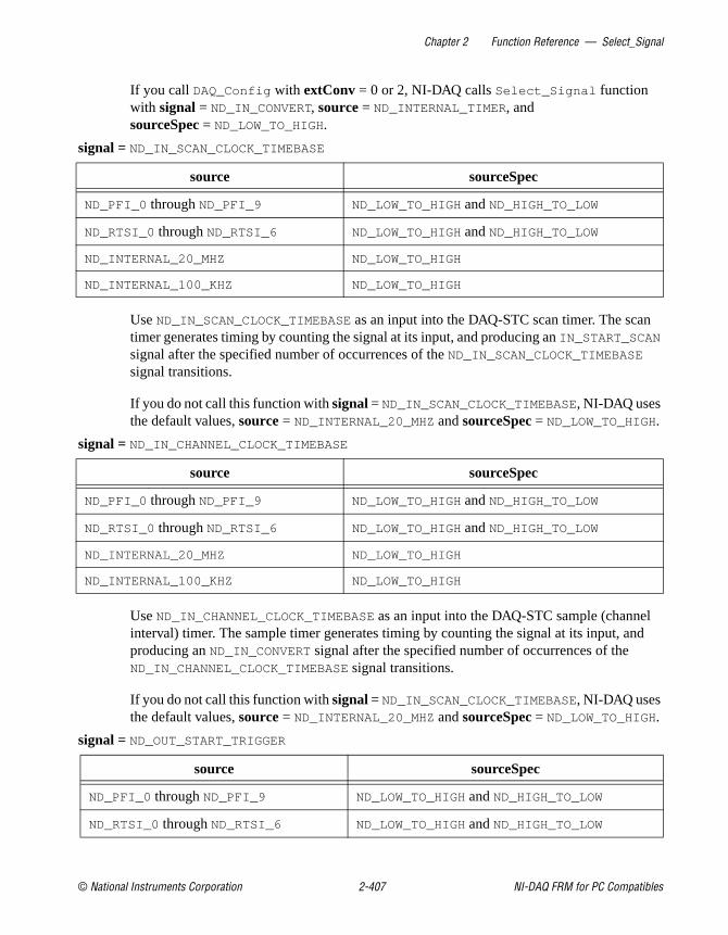
Chapter 2 Function Reference — Select_Signal
© National Instruments Corporation 2-407 NI-DAQ FRM for PC Compatibles
If you call DAQ_Config with extConv = 0 or 2, NI-DAQ calls Select_Signal function with signal = ND_IN_CONVERT, source = ND_INTERNAL_TIMER, and sourceSpec= ND_LOW_TO_HIGH.
signal = ND_IN_SCAN_CLOCK_TIMEBASE
Use ND_IN_SCAN_CLOCK_TIMEBASE as an input into the DAQ-STC scan timer. The scan timer generates timing by counting the signal at its input, and producing an IN_START_SCAN signal after the specified number of occurrences of the ND_IN_SCAN_CLOCK_TIMEBASE signal transitions.
If you do not call this function with signal = ND_IN_SCAN_CLOCK_TIMEBASE, NI-DAQ uses the default values, source = ND_INTERNAL_20_MHZ and sourceSpec= ND_LOW_TO_HIGH.
signal = ND_IN_CHANNEL_CLOCK_TIMEBASE
Use ND_IN_CHANNEL_CLOCK_TIMEBASE as an input into the DAQ-STC sample (channel interval) timer. The sample timer generates timing by counting the signal at its input, and producing an ND_IN_CONVERT signal after the specified number of occurrences of the ND_IN_CHANNEL_CLOCK_TIMEBASE signal transitions.
If you do not call this function with signal = ND_IN_SCAN_CLOCK_TIMEBASE, NI-DAQ uses the default values, source = ND_INTERNAL_20_MHZ and sourceSpec= ND_LOW_TO_HIGH.
signal = ND_OUT_START_TRIGGER
source sourceSpec
ND_PFI_0 through ND_PFI_9 ND_LOW_TO_HIGH and ND_HIGH_TO_LOW
ND_RTSI_0 through ND_RTSI_6 ND_LOW_TO_HIGH and ND_HIGH_TO_LOW
ND_INTERNAL_20_MHZ ND_LOW_TO_HIGH
ND_INTERNAL_100_KHZ ND_LOW_TO_HIGH
source sourceSpec
ND_PFI_0 through ND_PFI_9 ND_LOW_TO_HIGH and ND_HIGH_TO_LOW
ND_RTSI_0 through ND_RTSI_6 ND_LOW_TO_HIGH and ND_HIGH_TO_LOW
ND_INTERNAL_20_MHZ ND_LOW_TO_HIGH
ND_INTERNAL_100_KHZ ND_LOW_TO_HIGH
source sourceSpec
ND_PFI_0 through ND_PFI_9 ND_LOW_TO_HIGH and ND_HIGH_TO_LOW
ND_RTSI_0 through ND_RTSI_6 ND_LOW_TO_HIGH and ND_HIGH_TO_LOW

Chapter 2 Function Reference — Select_Signal
NI-DAQ FRM for PC Compatibles 2-408 www.natinst.com
Use ND_OUT_START_TRIGGER to initiate a waveform generation sequence. You can use an external signal or the signal used as the ND_IN_START_TRIGGER, or NI-DAQ can generate it. Setting source to ND_IN_START_TRIGGER is useful for synchronizing waveform generation with data acquisition.
If you do not call this function with signal = ND_OUT_START_TRIGGER, NI-DAQ uses the default values, source = ND_AUTOMATIC and sourceSpec= ND_LOW_TO_HIGH.
signal = ND_OUT_UPDATE
Use this signal for update timing. You can use a DAQ-STC timer for timing the updates, or you can use an external signal. You also can use output of the general-purpose counter 1 for update timing.
If you do not call this function with signal = ND_OUT_UPDATE, NI-DAQ uses the default values, source = ND_INTERNAL_TIMER and sourceSpec= ND_LOW_TO_HIGH.
signal = ND_OUT_EXTERNAL_GATE
Use this signal for gating the waveform generation. For example, if you call this function withsignal =ND_OUT_EXTERNAL_GATE, source = ND_PFI_9 , and sourceSpec= ND_PAUSE_ON_HIGH, the waveform generation will be paused whenever the PFI 9 is at the high level.
ND_IN_START_TRIGGER ND_LOW_TO_HIGH
ND_AUTOMATIC ND_LOW_TO_HIGH
ND_IO_CONNECTOR ND_LOW_TO_HIGH
source sourceSpec
ND_PFI_0 through ND_PFI_9 ND_LOW_TO_HIGH and ND_HIGH_TO_LOW
ND_RTSI_0 through ND_RTSI_6 ND_LOW_TO_HIGH and ND_HIGH_TO_LOW
ND_GPCTR1_OUTPUT ND_LOW_TO_HIGH and ND_HIGH_TO_LOW
ND_INTERNAL_TIMER ND_LOW_TO_HIGH
source sourceSpec
ND_PFI_0 through ND_PFI_9 ND_PAUSE_ON_HIGH and ND_PAUSE_ON_LOW
ND_RTSI_0 through ND_RTSI_6 ND_PAUSE_ON_HIGH and ND_PAUSE_ON_LOW
ND_NONE ND_DONT_CARE
source sourceSpec

Chapter 2 Function Reference — Select_Signal
© National Instruments Corporation 2-409 NI-DAQ FRM for PC Compatibles
If you do not call this function with signal = ND_OUT_EXTERNAL_GATE, NI-DAQ uses the default values, source = ND_NONE and sourceSpec = ND_DONT_CARE; therefore, by default, the waveform generation is not gated.
signal = ND_OUT_UPDATE_CLOCK_TIMEBASE
Use this signal as an input into the DAQ-STC update timer. The update timer generates timing by counting the signal at its input and producing an ND_OUT_UPDATE signal after the specified number of occurrences of the ND_OUT_UPDATE_CLOCK_TIMEBASE signal transitions.
If you do not call this function with signal = ND_OUT_UPDATE_CLOCK_TIMEBASE, NI-DAQ uses the default values, source = ND_INTERNAL_20_MHZ and sourceSpec= ND_LOW_TO_HIGH.
signal = ND_PFI_0 through ND_PFI_9
The following table summarizes all the signals and source for the I/O connector pins PFI0 through PFI9.
source sourceSpec
ND_PFI_0 through ND_PFI_9 ND_LOW_TO_HIGH and ND_HIGH_TO_LOW
ND_RTSI_0 through ND_RTSI_6 ND_LOW_TO_HIGH and ND_HIGH_TO_LOW
ND_INTERNAL_20_MHZ ND_LOW_TO_HIGH
ND_INTERNAL_100_KHZ ND_LOW_TO_HIGH
signal source sourceSpec
ND_PFI_0 through ND_PFI_9
ND_NONE ND_DONT_CARE
ND_PFI_0 ND_IN_START_TRIGGER ND_LOW_TO_HIGH
ND_PFI_1 ND_IN_STOP_TRIGGER ND_LOW_TO_HIGH
ND_PFI_2 ND_IN_CONVERT Refer to the Special Considerations when source = ND_CONVERT section for more information.
ND_HIGH_TO_LOW
ND_PFI_3 ND_GPCTR1_SOURCE ND_LOW_TO_HIGH
ND_PFI_4 ND_GPCTR1_GATE ND_POSITIVE
ND_PFI_5 ND_OUT_UPDATE ND_HIGH_TO_LOW
ND_PFI_6 ND_OUT_START_TRIGGER ND_LOW_TO_HIGH
ND_PFI_7 ND_IN_SCAN_START ND_LOW_TO_HIGH

Chapter 2 Function Reference — Select_Signal
NI-DAQ FRM for PC Compatibles 2-410 www.natinst.com
Use ND_NONE to disable output on the pin.
signal = ND_GPCTR0_OUTPUT
Use ND_NONE to disable output on the pin. When you disable output on this pin, you can use the pin as an input pin, and you can attach an external signal to it. This is useful because it enables you to communicate a signal from the I/O connector to the RTSI bus.
When you enable this pin for output, you can program it to output the signal present at any one of the RTSI bus trigger lines or the general-purpose counter 0 output. The RTSI selections are useful because they enable you to communicate a signal from the RTSI bus to the I/O connector.
signal = ND_GPCTR1_OUTPUT
Use ND_NONE to disable the output on the pin; in other words, do place the pin in high impedance state.
NI-DAQ can use ND_RESERVED when you use this device with some of the SCXI modules. In this case, you can use general-purpose counter 1, but the output will not be available on the I/O connector because the pin is used for device-to-SCXI communication. Currently, there are no SCXI modules that require this.
ND_PFI_7 ND_IN_SCAN_IN_PROG ND_LOW_TO_HIGH
ND_PFI_8 ND_GPCTR0_SOURCE ND_LOW_TO_HIGH
ND_PFI_9 ND_GPCTR0_GATE ND_POSITIVE
source sourceSpec
ND_NONE ND_DONT_CARE
ND_GPCTR0_OUTPUT ND_LOW_TO_HIGH
ND_RTSI_0 through ND_RTSI_6 ND_LOW_TO_HIGH
source sourceSpec
ND_NONE ND_DONT_CARE
ND_GPCTR1_OUTPUT ND_LOW_TO_HIGH
ND_RESERVED ND_DONT_CARE
signal source sourceSpec

Chapter 2 Function Reference — Select_Signal
© National Instruments Corporation 2-411 NI-DAQ FRM for PC Compatibles
signal = ND_FREQ_OUT
Use ND_NONE to disable the output on the pin; in other words, to place the pin in high impedance state.
The signal present on the FREQ_OUT pin of the I/O connector is the divided-down version of one of the two internal timebases. Use sourceSpec to specify the divide-down factor.
signal = ND_SCANCLK_LINE
Note This information applies to E Series boards only.
When source = ND_SCANCLK, the signal provided by the E Series board to time operation of certain classes of external accessories, such as external multiplexers or signal conditioning circuits, appears at the SCANCLK pin on the IO connector. This signal pulses once each time and A/D conversion is performed. When source = ND_NONE, the signal is disabled. If you have and NI accessory that requires this signal, NI-DAQ will automatically enable it as needed. Refer to your E Series User Manual for further details about this signal.
signal = ND_RTSI_0 through ND_RTSI_6
source sourceSpec
ND_NONE ND_DONT_CARE
ND_INTERNAL_10_MHZ 1 through 16
ND_INTERNAL_100_KHZ 1 through 16
source sourceSpec
ND_SCANCLK ND_LOW_TO_HIGH
ND_NONE ND_DONT_CARE
source sourceSpec
ND_NONE ND_DONT_CARE
ND_IN_START_TRIGGER ND_LOW_TO_HIGH
ND_IN_STOP_TRIGGER ND_LOW_TO_HIGH
ND_IN_CONVERT ND_HIGH_TO_LOW
ND_OUT_UPDATE ND_HIGH_TO_LOW
ND_OUT_START_TRIGGER ND_LOW_TO_HIGH
ND_GPCTR0_SOURCE ND_LOW_TO_HIGH

Chapter 2 Function Reference — Select_Signal
NI-DAQ FRM for PC Compatibles 2-412 www.natinst.com
Note This information applies to E Series devices only.
When source = ND_IN_SCAN_START, the actual signal source on the specified RTSI line is ND_IN_SCAN_START or ND_IN_SCAN_IN_PROG. The default signal source is ND_IN_SCAN_START, with source = ND_IN_SCAN_START. The following actions will change the signal source:
• Call the select_signal function with signal = ND_PFI_7 and source= ND_IN_SCAN_START or ND_SCAN_IN_PROG.
Note Disabling the output on the PFI7 line (by calling Select_Signal with signal = ND_PFI_7 and source = ND_NONE) and then calling Select_Signal with signal = ND_RTSI_i (where i= 0 – 6) and source = ND_IN_SCAN_START will result in ND_IN_SCAN_START being driven on the specified RTSI line regardless of what source was used to drive the PFI7 line in any previous Select_Signal call.
• Configuring some external devices, such as the SC-2040, causes the ND_IN_SCAN_IN_PROG signal to be output on the PFI7 line. This causes an ensuing call to Select_Signal with signal = ND_RTSI_i and source = ND_IN_SCAN_START to drive ND_IN_SCAN_IN_PROG onto the specified RTSI line.
You can use the GPCTR0_OUTPUT pin on the I/O connector in two ways—as an output pin or an input pin. When you configure the pin as an output pin, you can program the pin to output a signal from a RTSI line or the general-purpose counter 0 output (see signal = ND_GPCTR0_OUTPUT in this function for details). When you configure the pin as an input pin, you can attach an external signal to the pin. When signal is one of the RTSI lines, and source= ND_GPCTR0_OUTPUT, the signal on the RTSI line will be the signal present at the GPCTR0_OUTPUT pin on the I/O connector, which is not always the output of the general-purpose counter 0.
signal = ND_RTSI_CLOCK
ND_GPCTR0_GATE ND_POSITIVE
ND_GPCTR0_OUTPUT ND_DONT_CARE
ND_IN_SCAN_START ND_LOW_TO_HIGH
source sourceSpec
ND_NONE ND_DONT_CARE
ND_BOARD_CLOCK ND_DONT_CARE
source sourceSpec

Chapter 2 Function Reference — Select_Signal
© National Instruments Corporation 2-413 NI-DAQ FRM for PC Compatibles
Use source = ND_NONE to stop the device from driving the RTSI clock line.
When source = ND_BOARD_CLOCK, this device drives the signal on the RTSI clock line.
signal = ND_BOARD_CLOCK
Use source = ND_BOARD_CLOCK to stop the device from receiving the clock signal from the RTSI clock line.
Use source = ND_RTSI_CLOCK to program the device to receive the clock signal from the RTSI clock line.
signal = ND_PLL_REF_SOURCE
Use ND_NONE for internal calibrated reference.
By using ND_IO_CONNECTOR, you can select an external reference clock to be the source for the phase-locked loop (PLL), or you can use ND_RTSI_CLOCK when running at 20 MHz to be the reference clock source for the PLL. By default, NI-DAQ selects the internal reference.
Special Considerations when source = ND_CONVERTWhen you enable the convert signal to go out on PFI_2 or any of the RTSI lines, there is a pulse prior to the start of data acquisition. This is the side effect of programming the device for data acquisition, and the receiver of the signal should keep this in mind. For example, to synchronize two devices using the convert signal, you should also make them share the start trigger signal so that the spurious convert pulse generated by the controlling device is ignored by the controlling device.
source sourceSpec
ND_BOARD_CLOCK ND_DONT_CARE
ND_RTSI_CLOCK ND_DONT_CARE
source sourceSpec
ND_RTSI_CLOCK ND_DONT_CARE
ND_IO_CONNECTOR ND_DONT_CARE
ND_NONE (default) ND_DONT_CARE

Chapter 2 Function Reference — Select_Signal
NI-DAQ FRM for PC Compatibles 2-414 www.natinst.com
Parameter Discussion for the 660X DevicesLegal ranges for the signal, source, and sourceSpec parameters are given in terms of constants that are defined in a header file.
• BASIC programmers—NIDAQCNS.INC (Visual Basic for Windows programmers should refer to the Programming Language Considerations section in Chapter 1, Using the NI-DAQ Functions, for more information.)
• Pascal programmers—NIDAQCNS.PAS
Note Use the signal parameter to specify the signal whose source you want to select. The following table shows the possible values for signal.
Legal values for source and sourceSpec depend on the signal and are shown in the following tables:
signal = ND_RTSI_0 through ND_RTSI_6 and ND_RTSI_CLOCK
Table 2-31. Legal Parameters for the 660X Devices
Group Signal Description
All of the RTSI lines ND_RTSI_0 through ND_RTSI_6 and ND_RTSI_CLOCK
Selects a counter for output on a RTSI line
The triggering input for the counter
ND_START_TRIGGER Selects a source for the hardware arming or triggering source of the counter
PFI lines ND_PFI_LINE_0 through ND_PFI_LINE_39
Sets PFI line to an input or output state
Configurable digital filter ND_CONFIGURABLE_FILTER Selects the signal to be used as a digital filter for PFI lines.
Board timing ND_BOARD_CLOCK Allows two boards to use the same clock
(PXI-6608 only) PXI chassis backplane lines
ND_PXI_BACKPLANE_CLOCK Allows the board to drive the PXI backplane clock.
source sourceSpec
ND_NONE (default) ND_DONT_CARE
ND_LOW ND_DONT_CARE
ND_HIGH ND_DONT_CARE

Chapter 2 Function Reference — Select_Signal
© National Instruments Corporation 2-415 NI-DAQ FRM for PC Compatibles
You can use the internal, highly stable 10 MHz oscillator (only on 6608 devices) as the source (or gate) of any counter by routing the clock to any of the RTSI lines and then using that RTSI line as the source (or gate) for that counter.
Example/* first route the 10 MHz clock to RTSI line 0 */
status = Select_Signal (1, ND_RTSI_0, ND_STABLE_10_MHZ,
ND_DONT_CARE);
/* next route the RTSI line 0 to the source of counter 1 */
status = GPCTR_Change_Parameter (1, 1, ND_SOURCE, ND_RTSI_0);
This example shows how to use stable 10 MHz clock as the source of counter 1.
(PXI-6608 devices only)—The PXI-6608 device, when plugged into the star-controller slot (slot 2), automatically drives the RTSI_6 line with its internal, stable 10 MHz oscillator (ND_STABLE_10_MHZ) during initialization. This in turn drives the PXI backplane clock (PXI_CLK10). In this case, you can directly use the RTSI_6 line as the source or gate of any counter. You can also use any of the other RTSI lines to route the stable 10 MHz clock as shown in the previous example. When plugged into a non-star controller slot (slots 3 and higher), the PXI-6608 does not drive the PXI backplane clock. Instead, you can use the RTSI_6 line to drive the PXI_STAR line in the PXI backplane for advanced timing and triggering applications. Refer to Table 2-32, Descriptions for application and your hardware user manual for details.
signal = ND_START_TRIGGER
ND_GPCTR0_OUTPUT through ND_GPCTR7_OUTPUT ND_DONT_CARE
ND_BOARD_CLOCK (only when signal = ND_RTSI_CLOCK) ND_DONT_CARE
ND_STABLE_10_MHZ (only for 6608 devices) ND_DONT_CARE
source sourceSpec
ND_LOW ND_DONT_CARE
ND_HIGH ND_DONT_CARE
ND_PFI_0 through ND_PFI_39 ND_LOW_TO_HIGH or ND_HIGH_TO_LOW
ND_RTSI_0 through ND_RTSI_6 and ND_RTSI_CLOCK ND_LOW_TO_HIGH or ND_HIGH_TO_LOW
source sourceSpec

Chapter 2 Function Reference — Select_Signal
NI-DAQ FRM for PC Compatibles 2-416 www.natinst.com
Examplestatus = Select_Signal (1, ND_START_TRIGGER, ND_RTSI_5,
ND_LOW_TO_HIGH);
This example would route RTSI_5 to be the start trigger for the counters on a 6602 device. An active edge on RTSI_5 starts all counters that await a START_TRIGGER. The software start must be issued to the counter before the start trigger will work. A counter is configured to start upon receiving a start trigger through a GPCTR_Change parameter call with paramID = ND_START_TRIGGER and paramValue = ND_ENABLED.
signal = ND_BOARD_CLOCK
Use source = ND_BOARD_CLOCK to stop the device from receiving the clock signal from the RTSI clock line.
Use source = ND_RTSI_CLOCK to program the device to receive the clock signal from the RTSI clock line. This parameter makes the signal on the RTSI clock line replace the internal 20 MHz timebase signal on the board. As a result, the RTSI clock signal is routed to wherever the internal 20 MHz timebase was previously routed. In addition, the frequency of the 100 KHz internal timebase equals the RSTI_CLOCK frequency divided by 200. These changes to the internal 20 MHz and 100 KHz timebases may affect some of your calculations based on counter values.
signal = ND_CONFIGUREABLE_FILTER
The configurable filter gives PFI lines a more flexible way of selecting their digital filter.
Examplestatus = Select_Signal (1, ND_CONFIGURABLE_FILTER, ND_RTSI_0,
ND_DONT_CARE);
status = Line_Change_Attribute (1, ND_PFI_0, ND_LINE_FILTER,
ND_CONFIGURABLE_FILTER);
This example shows how to set up the configurable filter. Signals coming in on PFI line 0 will be filtered based upon the frequency of the signal on RTSI line 0.
source sourceSpec
ND_BOARD_CLOCK ND_DONT_CARE
ND_RTSI_CLOCK ND_DONT_CARE
source sourceSpec
ND_RTSI_0 through ND_RTSI_6 andND_RTSI_CLOCK
ND_DONT_CARE

Chapter 2 Function Reference — Select_Signal
© National Instruments Corporation 2-417 NI-DAQ FRM for PC Compatibles
signal = ND_PFI_0 through ND_PFI_39
signal source sourceSpec
ND_PFI_0 through ND_PFI_7 ND_NONE (default) ND_DONT_CARE
ND_PFI_8 ND_GPCTR7_OUTPUT(default), ND_NONE
ND_DONT_CARE
ND_PFI_9 ND_NONE (default)
ND_PFI_10 ND_NONE (default), ND_GPCTR7_GATE
ND_PFI_11 ND_NONE (default), ND_GPCTR7_SOURCE
ND_DONT_CARE
ND_PFI_12 ND_GPCTR6_OUTPUT(default), ND_NONE
ND_DONT_CARE
ND_PFI_13 ND_NONE (default)
ND_PFI_14 ND_NONE (default), ND_GPCTR6_GATE
ND_PFI_15 ND_NONE (default), ND_GPCTR6_SOURCE
ND_DONT_CARE
ND_PFI_16 ND_GPCTR5_OUTPUT (default), ND_NONE
ND_DONT_CARE
ND_PFI_17 ND_NONE (default)
ND_PFI_18 ND_NONE (default), ND_GPCTR5_GATE
ND_PFI_19 ND_NONE (default), ND_GPCTR5_SOURCE
ND_DONT_CARE
ND_PFI_20 ND_GPCTR4_OUTPUT(default), ND_NONE
ND_DONT_CARE
ND_PFI_21 ND_NONE(default)
ND_PFI_22 ND_NONE (default), ND_GPCTR4_GATE
ND_PFI_23 ND_NONE (default), ND_GPCTR4_SOURCE
ND_DONT_CARE

Chapter 2 Function Reference — Select_Signal
NI-DAQ FRM for PC Compatibles 2-418 www.natinst.com
ND_PFI_24 ND_GPCTR3_OUTPUT(default), ND_NONE
ND_DONT_CARE
ND_PFI_25 ND_NONE (default)
ND_PFI_26 ND_NONE (default), ND_GPCTR3_GATE
ND_PFI_27 ND_NONE (default), ND_GPCTR3_SOURCE
ND_DONT_CARE
ND_PFI_28 ND_GPCTR2_OUTPUT(default), ND_NONE
ND_DONT_CARE
ND_PFI_29 ND_NONE (default)
ND_PFI_30 ND_NONE (default), ND_GPCTR2_GATE
ND_PFI_31 ND_NONE (default), ND_GPCTR2_SOURCE
ND_DONT_CARE
ND_PFI_32 ND_GPCTR1_OUTPUT(default), ND_NONE
ND_DONT_CARE
ND_PFI_33 ND_NONE (default) ND_DONT_CARE
ND_PFI_34 ND_NONE (default), ND_GPCTRI_GATE
ND_DONT_CARE
ND_PFI_35 ND_NONE (default), ND_GPCTR1_SOURCE
ND_DONT_CARE
ND_PFI_36 ND_INTERNAL_LINE_0,
ND_INTERNAL_LINE_8,
ND_GPCTR0_OUTPUT(default), ND_NONE
ND_DONT_CARE
ND_PFI_37 ND_NONE (default) ND_DONT_CARE
ND_PFI_38 ND_NONE (default), ND_GPCTR0_GATE
ND_DONT_CARE
ND_PFI_39 ND_NONE (default), ND_GPCTR0_SOURCE
ND_DONT_CARE
signal source sourceSpec

Chapter 2 Function Reference — Select_Signal
© National Instruments Corporation 2-419 NI-DAQ FRM for PC Compatibles
Most IO pins on the 6602 boards are capable of doing input and output.
Examplestatus = Select_Signal (1, ND_PFI_24, ND_GPCTR3_OUTPUT,
ND_DONT_CARE);
For PXI-6608 device onlysignal = ND_PXI_BACKPLANE_CLOCK
The PXI chassis has a 10 MHz clock line (PXI_CLK10 ) in its backplane which allows boards plugged in the non-star controller slots (slots 3 and higher) to phase-lock their oscillators to the backplane clock. This way the drift in the oscillators on all the boards in the non-star controller slots can be controlled by a single backplane clock. The PXI-6608 device when plugged in the star-controller slot (slot 2) automatically drives the PXI backplane clock with its much more stable oscillator. Alternatively, when plugged in one of the non-star controller slots (slots 3 and higher) the PXI-6608 automatically phase-locks its oscillator to the backplane clock. You can use the above call with source = ND_NONE to disable or source= ND_STABLE_10_MHZ to enable the 6608 from driving the backplane clock. This call is valid only if the PXI-6608 is plugged in the star-controller slot (slot 2) of the PXI chassis.
Using This FunctionIf you have selected a signal that is not an I/O connector pin, pin or a RTSI bus line, Select_Signal saves the parameters in the configuration tables for future operations. Functions that initiate data acquisition (DAQ_Start , SCAN_Start , DAQ_Op, and SCAN_Op) and waveform generation operations (WFM_Group_Control and WFM_Op) use the configuration tables to set the device circuitry to the correct timing modes.
You do not need to call this function if you are satisfied with the default settings for the signals.
If you have selected a signal that is an I/O connector signal or a RTSI bus signal, Select_Signal performs signal routing and enables or disables output on a pin or a RTSI line.
source sourceSpec
ND_STABLE_10_MHZ ND_DONT_CARE
ND_NONE ND_DONT_CARE

Chapter 2 Function Reference — Select_Signal
NI-DAQ FRM for PC Compatibles 2-420 www.natinst.com
ExampleTo send a signal from your E Series device to the RTSI bus, set signal to the appropriate RTSI bus line and source to indicate the signal from your device. If you want to send the analog input start trigger on to RTSI line 3, use the following call:
Select_Signal(deviceNum, ND_RTSI_3, ND_IN_START_TRIGGER,
ND_LOW_TO_HIGH)
Example To receive a signal from the RTSI bus and use it as a signal on your E Series device, set signal to indicate the appropriate E Series device signal and source to the appropriate RTSI line. If you want to use low-to-high transitions of the signal present on the RTSI line 4 as your scan clock, use the following call:
Select_Signal(deviceNum, ND_IN_SCAN_START, ND_RTSI_4, ND_LOW_TO_HIGH)
Signal Name EquivalenciesFor a variety of reasons, some timing signals are given different names in the hardware documentation and the software and its documentation. The following table lists the equivalencies between the two sets of signal names.
Table 2-32. E Series and 671X Signal Name Equivalencies
Signals Hardware Name Software Name
AI-Related TRIG1 ND_IN_START_TRIGGER
TRIG2 ND_IN_STOP_TRIGGER
STARTSCAN ND_IN_SCAN_START
SISOURCE ND_IN_SCAN_CLOCK_TIMEBASE
CONVERT* ND_IN_CONVERT
AIGATE ND_IN_EXTERNAL_GATE
SI2SOURCE ND_IN_CHANNEL_CLOCK_TIMEBASE
AO-Related WFTRIG ND_OUT_START_TRIGGER
UPDATE* ND_OUT_UPDATE
AOGATE ND_OUT_EXTERNAL_GATE
UISOURCE ND_OUT_UPDATE_CLOCK_TIMEBASE
AO2GATE N/A
UI2SOURCE N/A

Chapter 2 Function Reference — Select_Signal
© National Instruments Corporation 2-421 NI-DAQ FRM for PC Compatibles
The VXI-MIO-64E-1 and VXI-MIO-64XE-10 devices use the VXIbus trigger lines to implement the RTSI bus synchronization between two or more such devices. The following table shows the mapping between the RTSI bus line (identifier) and the corresponding VXIbus trigger line.
Note Unpredictable behavior might result if other VXIbus devices simultaneously use the same VXIbus trigger line that the VXI-MIO devices are using to synchronize their operations.
Table 2-33. RTSI Bus Line and VXIbus Trigger Mapping
RTSI bus line identifier VXIbus trigger line
ND_RTSI_0 VXIbus TTL Trigger 0 (TTLTRG0)
ND_RTSI_1 VXIbus TTL Trigger 1 (TTLTRG1)
ND_RTSI_2 VXIbus TTL Trigger 2 (TTLTRG2)
ND_RTSI_3 VXIbus TTL Trigger 3 (TTLTRG3)
ND_RTSI_4 VXIbus TTL Trigger 4 (TTLTRG4)
ND_RTSI_5 VXIbus ECL Trigger 0 (ECLTRG0)
ND_RTSI_6 VXIbus ECL Trigger 1 (ECLTRG1)
ND_RTSI_CLOCK VXIbus ECL Trigger 0 (ECLTRG0)
Table 2-34. RTSI Bus Line and PXI Bus Trigger Mapping
RTSI bus line identifier PXI bus trigger line
ND_RTSI_0 PXI Trigger 0
ND_RTSI_1 PXI Trigger 1
ND_RTSI_2 PXI Trigger 2
ND_RTSI_3 PXI Trigger 3
ND_RTSI_4 PXI Trigger 4
ND_RTSI_5 PXI Trigger 5
ND_RTSI_6 PXI Star
ND_RTSI_CLOCK PXI Trigger 7

Chapter 2 Function Reference — Select_Signal
NI-DAQ FRM for PC Compatibles 2-422 www.natinst.com
Note Unpredictable behavior might result if other PXI devices simultaneously use the same PXI trigger line that the PXI DAQ devices are using to synchronize their operations.
Note PXI trigger 6 line is not connected to any of the RTSI lines on all PXI boards.

Chapter 2 Function Reference — Set_DAQ_Device_Info
© National Instruments Corporation 2-423 NI-DAQ FRM for PC Compatibles
Set_DAQ_Device_Info
Formatstatus = Set_DAQ_Device_Info (deviceNumber, infoType, infoValue)
PurposeChanges the data transfer mode (interrupts and DMA) for certain classes of data acquisition operations, some settings for an SC-2040 track-and-hold accessory and an SC-2043-SG strain-gauge accessory, as well as the source for the CLK1 signal on the DAQCard-700.
ParametersInput
Parameter DiscussionLegal ranges for the infoType and infoValue are given in terms of constants that are defined in a header file. The header file you should use depends on which of the following languages you are using:
• C programmers—NIDAQCNS.H (DATAACQ.H for LabWindows/CVI)
• BASIC programmers—NIDAQCNS.INC (Visual Basic for Windows programmers should refer to the Programming Language Considerations section in Chapter 1, Using the NI-DAQ Functions, for more information.)
• Pascal programmers—NIDAQCNS.PAS
infoType indicates which parameter you want to change. Use infoValue to specify the corresponding new value.
Values that infoType accepts depend on the device you are using. The legal range for infoValue depends on the device you are using and infoType.
Name Type Description
deviceNumber i16 assigned by configuration utility
infoType u32 parameter you want to modify
infoValue u32 new value you want to assign to the parameter specified by infoType

Chapter 2 Function Reference — Set_DAQ_Device_Info
NI-DAQ FRM for PC Compatibles 2-424 www.natinst.com
infoType can be one of the following:
infoType Description
ND_ACK_REQ_EXCHANGE_GR1ND_ACK_REQ_EXCHANGE_GR2
Used to exchange the ACK and REQ pins on the DIO 6533 (DIO-32HS) connector
ND_AI_FIFO_INTERRUPTS Used to select method of AI interrupt generation
ND_CALIBRATION_ENABLE Used to enable or disable writes to the calibration channels
ND_CLOCK_REVERSE_MODE_GR1ND_CLOCK_REVERSE_MODE_GR2
Used to reverse the PCLK clock direction on the DIO 6533 (DIO-32HS) in burst handshaking mode
ND_COUNTER_1_SOURCE Used to select a source for counter 1 on the DAQCard-700
ND_DATA_XFER_MODE_AI Method NI-DAQ uses for data transfers when performing the DAQ, MDAQ, and SCAN operations
ND_DATA_XFER_MODE_AO_GR1ND_DATA_XFER_MODE_AO_GR2
Method NI-DAQ uses for data transfers when performing the WFM operations which require buffers from the PC memory
ND_DATA_XFER_MODE_GPCTR0 Method NI-DAQ uses for data transfers when buffered GPCTR operations are used with the general-purpose counter 0
ND_DATA_XFER_MODE_GPCTR1 Method NI-DAQ uses for data transfers when buffered GPCTR operations are used with the general-purpose counter 1
ND_DATA_XFER_MODE_GPCTR2 Method NI-DAQ uses for data transfers when buffered GPCTR operations are used with the general-purpose counter
ND_DATA_XFER_MODE_GPCTR3 Method NI-DAQ uses for data transfers when buffered GPCTR operations are used with the general-purpose counter 3
ND_DATA_XFER_MODE_GPCTR4 Method NI-DAQ uses for data transfers when buffered GPCTR operations are used with the general-purpose counter 4
ND_DATA_XFER_MODE_GPCTR5 Method NI-DAQ uses for data transfers when buffered GPCTR operations are used with the general-purpose counter 5

Chapter 2 Function Reference — Set_DAQ_Device_Info
© National Instruments Corporation 2-425 NI-DAQ FRM for PC Compatibles
infoValue can be one of the following:
ND_DATA_XFER_MODE_GPCTR6 Method NI-DAQ uses for data transfers when buffered GPCTR operations are used with the general-purpose counter 6
ND_DATA_XFER_MODE_GPCTR7 Method NI-DAQ uses for data transfers when bufferedGPCTR operations are used with the general-purpose counter 7
ND_DATA_XFER_MODE_DIO_GR1ND_DATA_XFER_MODE_DIO_GR2ND_DATA_XFER_MODE_DIO_GR3ND_DATA_XFER_MODE_DIO_GR4ND_DATA_XFER_MODE_DIO_GR5ND_DATA_XFER_MODE_DIO_GR6ND_DATA_XFER_MODE_DIO_GR7ND_DATA_XFER_MODE_DIO_GR8
Method NI-DAQ uses for data transfers for the digital input and output operations with group N (1 to 8)
ND_SC_2040_MODE Used to enable or disable the track-and-hold circuitry on the SC-2040
ND_SC_2043_MODE Used to enable or disable the SC-2043-SG accessory
ND_SET_POWERUP_STATE Used to save the current channel values as the powerup values
ND_SUSPEND_POWER_STATE State of USB device power when your operating system enters power-saving/suspend mode
infoValue Description
ND_ACTIVE Suspends the supply of power to USB devices if the USB Port is also in powersave mode
ND_AUTOMATIC Lets NI-DAQ decide the type of FIFO interrupt based on the acquisition rate. This is the default
ND_INACTIVE Maintains the supply of power to USB devices even if the USB port is in powersave mode
ND_INTERRUPTS NI-DAQ uses interrupts for data transfer
ND_INTERNAL_TIMER Counter 1 uses the internal timer as the source for its CLK1 source
infoType Description

Chapter 2 Function Reference — Set_DAQ_Device_Info
NI-DAQ FRM for PC Compatibles 2-426 www.natinst.com
ND_INTERRUPT_EVERY_SAMPLE Generates interrupts on every sample regardless of the acquisition rate
ND_INTERRUPT_HALF_FIFO Generates interrupts only when the FIFO is half full, regardless of the acquisition rate
ND_IO_CONNECTOR Counter 1 uses the CLK1 signal from the I/O connector as the source for its CLK1 signal
ND_NONE Cancels the effects of having accidentally called the SC_2040_Config function
ND_NO_STRAIN_GAUGE Disables the SC-2043-SG accessory
ND_NO_TRACK_AND_HOLD Disables use of the track-and-hold circuitry on the SC-20401
ND_OFF Disables the ACK and REQ exchange or the reversal of the clock direction of the DIO 6533 (DIO-32HS)
ND_ON Exchanges the ACK and REQ pins or reverses the clock direction on the DIO 6533 (DIO-32HS)
ND_STRAIN_GAUGE Enables the SC-2043-SG accessory for strain-gauge measurements (no excitation on channel 0)
ND_STRAIN_GAUGE_EX0 Enables the SC-2043-SG accessory with excitation on channel 0
ND_TRACK_AND_HOLD Re-enables the track-and-hold circuitry on an SC-2040 if you have previously disabled it2
ND_UP_TO_1_DMA_CHANNEL NI-DAQ must use only one DMA channel; if the DMA channel is not available, NI-DAQ reports an error and it will not perform the operation
ND_UP_TO_2_DMA_CHANNELS NI-DAQ uses two DMA channels, if possible; otherwise, it uses one DMA channel, if one is available; if no DMA channels are available, NI-DAQ reports an error and it will not perform the operation
infoValue Description

Chapter 2 Function Reference — Set_DAQ_Device_Info
© National Instruments Corporation 2-427 NI-DAQ FRM for PC Compatibles
When NI-DAQ uses DMA channels for data transfers, it must have an interrupt level available for the device performing the transfers. In this case, NI-DAQ uses interrupts for DMA controller reprogramming and exception handling.
Using This FunctionYou can use this function to select the data transfer method for a given operation on a particular device. If you do not use this function, NI-DAQ decides on the data transfer method that typically takes maximum advantage of available resources.
All possible data transfer methods for the devices supported by NI-DAQ are listed below. If your device is not listed, none of the data transfer modes are applicable. The table also shows default values for data transfer modes and other settings. An asterisk indicates default value.
ND_FOREGROUND NI-DAQ performs data transfers through the CPU
1 You should use this setting to use the SC-2040 only as a preamplifier, without using track and hold.
2 With ND_NO_TRACK_AND_HOLD.
Device Type infoType infoValue
AT-AO-6/10 ND_DATA_XFER_MODE_AO_GR1 ND_INTERRUPTSND_UP_TO_1_DMA_CHANNEL*
ND_DATA_XFER_MODE_AO_GR2 ND_INTERRUPTS*
AT-DIO-32F ND_DATA_XFER_MODE_DIO_GR1ND_UP_TO_1_DMA_CHANNEL ND_UP_TO_2_DMA_CHANNELS*
ND_DATA_XFER_MODE_DIO_GR2ND_UP_TO_1_DMA_CHANNEL*
AT-DIO-32HS ND_DATA_XFER_MODE_DIO_GR1ND_INTERRUPTSND_UP_TO_1_DMA_CHANNELND_UP_TO_2_DMA_CHANNELS*
ND_DATA_XFER_MODE_DIO_GR2ND_INTERRUPTSND_UP_TO_1_DMA_CHANNELND_UP_TO_2_DMA_CHANNELS*
infoValue Description

Chapter 2 Function Reference — Set_DAQ_Device_Info
NI-DAQ FRM for PC Compatibles 2-428 www.natinst.com
PCI-DIO-32HSPXI-6533
ND_DATA_XFER_MODE_DIO_GR1ND_INTERRUPTSND_UP_TO_1_DMA_CHANNEL*
ND_DATA_XFER_MODE_DIO_GR2ND_INTERRUPTSND_UP_TO_1_DMA_CHANNEL*
ND_ACK_REQ_EXCHANGE_GR1 ND_ONND_OFF*
ND_ACK_REQ_EXCHANGE_GR2 ND_ONND_OFF*
ND_CLOCK_REVERSE_MODE_GR1ND_ONND_OFF*
ND_CLOCK_REVERSE_MODE_GR2ND_ONND_OFF*
DAQCard-6533 ND_DATA_XFER_MODE_DIO_GR1ND_INTERRUPTS*
ND_DATA_XFER_MODE_DIO_GR2ND_INTERRUPTS*
ND_ACK_REQ_EXCHANGE_GR1 ND_ONND_OFF*
ND_ACK_REQ_EXCHANGE_GR2 ND_ONND_OFF*
ND_CLOCK_REVERSE_MODE_GR1ND_ONND_OFF*
ND_CLOCK_REVERSE_MODE_GR2ND_ONND_OFF*
AT-MIO-16E-1 ND_DATA_XFER_MODE_AI ND_INTERRUPTS ND_UP_TO_1_DMA_CHANNELND_UP_TO_2_DMA_CHANNELS*
ND_DATA_XFER_MODE_AO_GR1 ND_INTERRUPTS ND_UP_TO_1_DMA_CHANNEL*
ND_DATA_XFER_MODE_GPCTR0 ND_INTERRUPTS ND_UP_TO_1_DMA_CHANNEL ND_UP_TO_2_DMA_CHANNELS*
ND_DATA_XFER_MODE_GPCTR1 ND_INTERRUPTS ND_UP_TO_1_DMA_CHANNEL ND_UP_TO_2_DMA_CHANNELS*
Device Type infoType infoValue

Chapter 2 Function Reference — Set_DAQ_Device_Info
© National Instruments Corporation 2-429 NI-DAQ FRM for PC Compatibles
AT-MIO-16E-2NEC-MIO-16E-4AT-MIO-64E-3
ND_DATA_XFER_MODE_AI ND_INTERRUPTS ND_UP_TO_1_DMA_CHANNEL*
ND_DATA_XFER_MODE_AO_GR1 ND_INTERRUPTS ND_UP_TO_1_DMA_CHANNEL*
ND_DATA_XFER_MODE_GPCTR0 ND_INTERRUPTS ND_UP_TO_1_DMA_CHANNEL ND_UP_TO_2_DMA_CHANNELS*
ND_DATA_XFER_MODE_GPCTR1 ND_INTERRUPTS ND_UP_TO_1_DMA_CHANNEL ND_UP_TO_2_DMA_CHANNELS*
PCI/PXI MIO E Series devices and MIO E Series devices for 1394
ND_DATA_XFER_MODE_AI ND_INTERRUPTSND_UP_TO_1_DMA_CHANNEL*
ND_DATA_XFER_MODE_AO_GR1
ND_INTERRUPTSND_UP_TO_1_DMA_CHANNEL*
ND_DATA_XFER_MODE_GPCTR0
ND_INTERRUPTSND_UP_TO_1_DMA_CHANNEL*
ND_DATA_XFER_MODE_GPCTR1
ND_INTERRUPTSND_UP_TO_1_DMA_CHANNEL*
ND_AI_FIFO_INTERRUPTS ND_AUTOMATIC*ND_INTERRUPT_EVERY_SAMPLEND_INTERRUPT_HALF_FIFO
PCI/PXI AI E Series devices and E Series devices for 1394
ND_DATA_XFER_MODE_AI ND_INTERRUPTSND_UP_TO_1_DMA_CHANNEL*
ND_DATA_XFER_MODE_GPCTR0
ND_INTERRUPTSND_UP_TO_1_DMA_CHANNEL*
ND_DATA_XFER_MODE_GPCTR1
ND_INTERRUPTSND_UP_TO_1_DMA_CHANNEL*
ND_AI_FIFO_INTERRUPTS ND_AUTOMATIC*ND_INTERRUPT_EVERY_SAMPLEND_INTERRUPT_HALF_FIFO
Device Type infoType infoValue

Chapter 2 Function Reference — Set_DAQ_Device_Info
NI-DAQ FRM for PC Compatibles 2-430 www.natinst.com
671X devices ND_DATA_XFER_MODE_AO_GR1
ND_INTERRUPTSND_UP_TO_1_DMA_CHANNEL*
ND_DATA_XFER_MODE_GPCTR0
ND_INTERRUPTSND_UP_TO_1_DMA_CHANNEL*
ND_DATA_XFER_MODE_GPCTR1
ND_INTERRUPTSND_UP_TO_1_DMA_CHANNEL*
AT-AI-16XE-10NEC-AI-16E-4NEC-AI-16XE-50
ND_DATA_XFER_MODE_GPCTR0
ND_INTERRUPTSND_UP_TO_1_DMA_CHANNEL*
ND_DATA_XFER_MODE_GPCTR1
ND_INTERRUPTSND_UP_TO_1_DMA_CHANNEL*
ND_DATA_XFER_MODE_GPCTR1 ND_INTERRUPTS ND_UP_TO_1_DMA_CHANNEL ND_UP_TO_2_DMA_CHANNELS*
AT-MIO-16E-10AT-MIO-16DE-10AT-MIO-16XE-10AT-MIO-16XE-50NEC-MIO-16XE-50
ND_DATA_XFER_MODE_AI ND_INTERRUPTS ND_UP_TO_1_DMA_CHANNEL
ND_DATA_XFER_MODE_AO_GR1 ND_INTERRUPTS ND_UP_TO_1_DMA_CHANNEL ND_UP_TO_2_DMA_CHANNELS*
ND_DATA_XFER_MODE_GPCTR0 ND_INTERRUPTS ND_UP_TO_1_DMA_CHANNEL ND_UP_TO_2_DMA_CHANNELS*
ND_DATA_XFER_MODE_GPCTR1 ND_INTERRUPTS ND_UP_TO_1_DMA_CHANNEL ND_UP_TO_2_DMA_CHANNELS*
DAQCard AI E Series devices
ND_DATA_XFER_MODE_AI ND_INTERRUPTS*
ND_DATA_XFER_MODE_GPCTR0 ND_INTERRUPTS*
ND_DATA_XFER_MODE_GPCTR1 ND_INTERRUPTS*
ND_AI_FIFO_INTERRUPTS ND_AUTOMATIC*ND_INTERRUPT_EVERY_SAMPLEND_INTERRUPT_HALF_FIFO
Device Type infoType infoValue

Chapter 2 Function Reference — Set_DAQ_Device_Info
© National Instruments Corporation 2-431 NI-DAQ FRM for PC Compatibles
DAQCard MIO E Series devices
ND_DATA_XFER_MODE_AI ND_INTERRUPTS*
ND_DATA_XFER_MODE_AO_GR1 ND_INTERRUPTS*
ND_DATA_XFER_MODE_GPCTR0 ND_INTERRUPTS*
ND_DATA_XFER_MODE_GPCTR1 ND_INTERRUPTS*
ND_AI_FIFO_INTERRUPTS ND_AUTOMATIC*ND_INTERRUPT_EVERY_SAMPLEND_INTERRUPT_HALF_FIFO
DAQPad-MIO-16XE-50 ND_DATA_XFER_MODE_AI ND_INTERRUPTS*
ND_DATA_XFER_MODE_AO_GR1 ND_INTERRUPTS*
ND_DATA_XFER_MODE_GPCTR0 ND_INTERRUPTS*
ND_DATA_XFER_MODE_GPCTR1 ND_INTERRUPTS*
ND_AI_FIFO_INTERRUPTS ND_INTERRUPT_EVERY_SAMPLE
ND_INTERRUPT_HALF_FIFOND_AUTOMATIC*
516 devicesDAQCard-500/700
ND_DATA_XFER_MODE_AI ND_INTERRUPTS*
DAQCard-700 ND_AI_FIFO_INTERRUPTS ND_INTERRUPT_EVERY_SAMPLE
ND_INTERRUPT_HALF_FIFOND_AUTOMATIC*
LPM devices ND_DATA_XFER_MODE_AI ND_INTERRUPTS*
Lab-PC+Lab-PC-1200PCI-1200 (Rev. D and later)
ND_DATA_XFER_MODE_AI ND_INTERRUPTS ND_UP_TO_1_DMA_CHANNEL*
ND_DATA_XFER_MODE_AO_GR1 ND_INTERRUPTS*
ND_AI_FIFO_INTERRUPTS ND_INTERRUPT_EVERY_SAMPLE
ND_INTERRUPT_HALF_FIFOND_AUTOMATIC*
Device Type infoType infoValue

Chapter 2 Function Reference — Set_DAQ_Device_Info
NI-DAQ FRM for PC Compatibles 2-432 www.natinst.com
DAQCard-1200DAQPad-1200PCI-1200 (Rev. C and earlier)SCXI-1200DAQPad-6020E
ND_DATA_XFER_MODE_AI ND_INTERRUPTS*
ND_DATA_XFER_MODE_AO_GR1 ND_INTERRUPTS*
ND_AI_FIFO_INTERRUPTS ND_AUTOMATIC*
ND_INTERRUPT_EVERY_SAMPLE
ND_INTERRUPT_HALF_FIFO
Lab-PC-1200AI ND-DATA_XFER_MODE_AI ND_INTERRUPTSND_UP_TO_1_DMA_CHANNEL*
ND_AI_FIFO_INTERRUPTS ND_INTERRUPT_EVERY_SAMPLE
ND_INTERRUPT_HALF_FIFOND_AUTOMATIC*
USB devices ND_SUSPEND_POWER_STATE ND_ACTIVEND_INACTIVE
VXI-MIO-64E-1VXI-MIO-64XE-10
ND_DATA_XFER_MODE_AI ND_INTERRUPTSND_UP_TO_1_DMA_CHANNEL*
ND_DATA_XFER_MODE_AO_GR1 ND_INTERRUPTSND_UP_TO_1_DMA_CHANNEL*
ND_DATA_XFER_MODE_GPCTR0 ND_INTERRUPTSND_UP_TO_1_DMA_CHANNEL*
ND_DATA_XFER_MODE_GPCTR1 ND_INTERRUPTSND_UP_TO_1_DMA_CHANNEL*
PCI-4451, PCI-4452, PCI-4453, PCI-4454
ND_DATA_XFER_MODE_AO_GR1 ND_UP_TO_1_DMA_CHANNEL
ND_DATA_XFER_MODE_GPCTR0 ND_INTERRUPTSND_UP_TO_1_DMA_CHANNEL
ND_DATA_XFER_MODE_GPCTR1 ND_INTERRUPTSND_UP_TO_1_DMA_CHANNEL
Device Type infoType infoValue
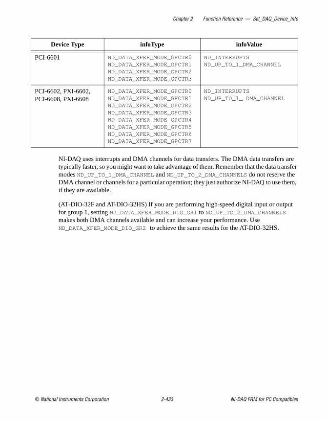
Chapter 2 Function Reference — Set_DAQ_Device_Info
© National Instruments Corporation 2-433 NI-DAQ FRM for PC Compatibles
NI-DAQ uses interrupts and DMA channels for data transfers. The DMA data transfers are typically faster, so you might want to take advantage of them. Remember that the data transfer modes ND_UP_TO_1_DMA_CHANNEL and ND_UP_TO_2_DMA_CHANNELS do not reserve the DMA channel or channels for a particular operation; they just authorize NI-DAQ to use them, if they are available.
(AT-DIO-32F and AT-DIO-32HS) If you are performing high-speed digital input or output for group 1, setting ND_DATA_XFER_MODE_DIO_GR1 to ND_UP_TO_2_DMA_CHANNELS makes both DMA channels available and can increase your performance. Use ND_DATA_XFER_MODE_DIO_GR2 to achieve the same results for the AT-DIO-32HS.
PCI-6601 ND_DATA_XFER_MODE_GPCTR0 ND_DATA_XFER_MODE_GPCTR1 ND_DATA_XFER_MODE_GPCTR2 ND_DATA_XFER_MODE_GPCTR3
ND_INTERRUPTS ND_UP_TO_1_DMA_CHANNEL
PCI-6602, PXI-6602, PCI-6608, PXI-6608
ND_DATA_XFER_MODE_GPCTR0ND_DATA_XFER_MODE_GPCTR1ND_DATA_XFER_MODE_GPCTR2ND_DATA_XFER_MODE_GPCTR3ND_DATA_XFER_MODE_GPCTR4ND_DATA_XFER_MODE_GPCTR5ND_DATA_XFER_MODE_GPCTR6ND_DATA_XFER_MODE_GPCTR7
ND_INTERRUPTSND_UP_TO_1_ DMA_CHANNEL
Device Type infoType infoValue

Chapter 2 Function Reference — Timeout_Config
NI-DAQ FRM for PC Compatibles 2-434 www.natinst.com
Timeout_Config
Formatstatus = Timeout_Config (deviceNumber, timeout)
PurposeEstablishes a timeout limit that is used by the synchronous functions to ensure that these functions eventually return control to your application. Examples of synchronous functions are DAQ_Op, DAQ_DB_Transfer and WFM_from_Disk .
ParametersInput
Parameter Discussiontimeout is the number of timer ticks. The duration of a tick is 55 ms (0.055 s), and there are approximately 18 ticks/s.
–1: Wait indefinitely (timeout disabled).0 to 231: Wait timeout * 0.055 s before returning.
Using This FunctionThe synchronous functions do not return control to your application until they have accomplished their task. If you have indicated a large amount of data and/or a slow acquisition or generation rate, you might want to terminate the function prematurely, short of restarting your computer. By calling Timeout_Config before calling the synchronous function, you can set an upper bound on the amount of time the synchronous function takes before returning. If the synchronous function returns the error code timeOutError , you know that the number of ticks indicated in the timeout parameter have elapsed and the synchronous function has returned because of the timeout.
The following is a list of the synchronous functions:
• DIG_DB_Transfer
• DAQ_DB_Transfer
• Lab_ISCAN_Op
• WFM_DB_Transfer
• DAQ_Op
Name Type Description
deviceNumber i16 assigned by configuration utility
timeout i32 number of timer ticks

Chapter 2 Function Reference — Timeout_Config
© National Instruments Corporation 2-435 NI-DAQ FRM for PC Compatibles
• Lab_ISCAN_to_Disk
• WFM_from_Disk
• DAQ_to_Disk
• SCAN_Op
• WFM_Op
• SCAN_to_Disk

Chapter 2 Function Reference — WFM_Chan_Control
NI-DAQ FRM for PC Compatibles 2-436 www.natinst.com
WFM_Chan_Control
Formatstatus = WFM_Chan_Control (deviceNumber, chan, operation)
PurposeTemporarily halts or restarts waveform generation for a single analog output channel.
ParametersInput
Parameter Discussionchan is the analog output channel to be paused or restarted.Range: 0 or 1 for most devices.
0 through 5 for AT-AO-6.0 through 9 for AT-AO-10.
operation selects the operation to be performed on the output channel.operation = 2 (PAUSE): Temporarily halts waveform generation for the output
channel. The last voltage available on the analog output channel is maintained indefinitely.
operation = 4 (RESUME): Restarts waveform generation for the output channel previously halted by operation = PAUSE.
Using This Function
Note This function does not support E Series or 671X devices.
When you have halted a waveform generation has been halted by executing PAUSE, the RESUME operation restarts the waveform exactly at the point in your buffer where it left off.
Name Type Description
deviceNumber i16 assigned by configuration utility
chan i16 analog output channel
operation i16 pause or resume

Chapter 2 Function Reference — WFM_Chan_Control
© National Instruments Corporation 2-437 NI-DAQ FRM for PC Compatibles
(AT-AO-6/10 only) You can use the PAUSE and RESUME operations on group 1 output channels only if at least one of the following conditions is true:
• Group 1 consists of a single output channel.
• Group 1 is using interrupts instead of DMA.
(AT-AO-6/10 only) You will see a FIFO lag effect when you pause or resume group 1 channels. When you execute PAUSE for a group 1 channel, the effective pause does not occur until the FIFO has finished writing all of the data remaining in the FIFO for the specified channel. The same is true for the RESUME operation on a group 1 channel. NI-DAQ cannot place data for the specified channel into the FIFO until the FIFO has emptied. Refer to the FIFO Lag Effect on the MIO E Series, AT-AO-6/10, PCI-4451, PCI-4453, and NI 4551 section of Chapter 3, Software Overview, of the NI-DAQ User Manual for PC Compatibles for a more detailed discussion.

Chapter 2 Function Reference — WFM_Check
NI-DAQ FRM for PC Compatibles 2-438 www.natinst.com
WFM_Check
Formatstatus = WFM_Check (deviceNumber, chan, wfmStopped, itersDone, pointsDone)
PurposeReturns status information concerning a waveform generation operation.
ParametersInput
Output
Parameter Discussionchan is the number of the analog output channel performing the waveform generation operation.Range: 0 or 1 for most devices.
0 through 5 for AT-AO-6.0 through 9 for AT-AO-10.0 through 3 for PCI-6711.0 through 7 for PCI-6713.
wfmStopped is a flag whose value indicates whether the waveform generation operation is still in progress. If the number of iterations indicated in the last WFM_Load call is 0, the status is always 0.
0: Ongoing operation.1: Complete operation.
itersDone returns the number of buffer iterations that have been completed.
Name Type Description
deviceNumber i16 assigned by configuration utility
chan i16 number of the analog output channel
Name Type Description
wfmStopped i16 whether the waveform is still in progress
itersDone u32 number of buffer iterations completed
pointsDone u32 number of points written for the current buffer iteration

Chapter 2 Function Reference — WFM_Check
© National Instruments Corporation 2-439 NI-DAQ FRM for PC Compatibles
pointsDone returns the number of points written to the analog output channels specified in chan for the current buffer iteration. For devices that have analog output FIFOs, pointsDone returns the number of points written to the FIFO if chan belongs to group 1. Refer to the following Using This Function section for more information.Range: 0 to count – 1, where count is the parameter used in the last WFM_Load call.
Note C Programmers—wfmStopped, itersDone, and pointsDone are pass-by-address parameters.
Using This FunctionWFM_Check returns status information concerning the progress of a waveform generation operation. It is useful in determining when an operation has completed and when you can initiate a new operation.
A FIFO lag effect is seen for group 1 channels on devices with analog output FIFOs. pointsDone and itersDone indicate the number of buffer points currently written to the FIFO. There is a time lag from the point when the data is written to the FIFO to when the data is output to the DACs. This time lag is dependent upon the update rate. For example, if you had a buffer of 50 points that you wanted to send to analog output channel 0, the first call to WFM_Check would have itersDone = 20. The FIFO would be filled up with 20 cycles of your 50-point buffer. Refer to the FIFO Lag Effect on the MIO E Series, AT-AO-6/10, PCI-4451, PCI-4453, and NI 4551 section of Chapter 3, Software Overview, of the NI-DAQ User Manual for PC Compatibles for a more detailed discussion. wfmStopped is also affected by the FIFO lag, since wfmStopped indicates when the last point has actually been output.
On the PCI/PXI/CPCI/1394 E Series and 671X devices, you can effectively turn off the FIFO to eliminate the FIFO by effect. Refer to the AO_Change_Parameter function.
Note E Series devices, AT-AO-6/10, PCI-4451, PCI-4453, and 671X devices only—If you use FIFO mode waveform generation, pointsDone is always 0. If the generation is continuous (including pulsed waveform generation), the parameters wfmStopped and itersDone are always 0; otherwise wfmStopped and itersDone indicate the status of waveform generation operation.

Chapter 2 Function Reference — WFM_ClockRate
NI-DAQ FRM for PC Compatibles 2-440 www.natinst.com
WFM_ClockRate
Formatstatus = WFM_ClockRate (deviceNumber, group, whichclock, timebase, interval, mode)
PurposeSets an update rate and a delay rate for a group of analog output channels.
ParametersInput
Parameter Discussiongroup is the group of analog output channels (see WFM_Group_Setup).Range: 1 for most devices.
1 or 2 for the AT-AO-6/10.
whichclock indicates the type of clock:0: The update clock (default).1: The delay clock.2: The delay clock prescalar 1 (E Series and 671X devices only).3: The delay clock prescalar 2 (E Series and 671X devices only).
Notice that you can program the delay clock only on the 671X and E Series devices.
timebase is the timebase, or resolution, NI-DAQ uses in determining interval . timebase has the following possible values:
–3: 20 MHz clock used as a timebase (50 ns) (E Series and 671X only).–1: 5 MHz clock used as timebase (200 ns resolution).0: If whichclock is equal to 0, the external clock is connected to EXTUPDATE on
the AT-AO-6/10 and Lab and 1200 Series analog output devices, or to a pin
Name Type Description
deviceNumber i16 assigned by configuration utility
group i16 group of analog output channels
whichclock i16 the update or delay clock
timebase i16 resolution
interval u32 timebase divisor
mode i16 enables the delay clock

Chapter 2 Function Reference — WFM_ClockRate
© National Instruments Corporation 2-441 NI-DAQ FRM for PC Compatibles
chosen through the Select_Signal function on an E Series and 671X device (default is PFI5).
1: 1 MHz clock used as timebase (1 µs resolution).2: 100 kHz clock used as timebase (10 µs resolution).3: 10 kHz clock used as timebase (100 µs resolution).4: 1 kHz clock used as timebase (1 ms resolution).5: 100 Hz clock used as timebase (10 ms resolution).
11: External timebase (E Series and 671X devices only).Connect your external timebase to PFI5, by default, or use the Select_Signal function to specify a different source.
On the Lab and 1200 Series analog output devices, timebase = 0 allows the signal applied to the EXTUPDATE pin on the I/O connector to control the DAC update. On the AT-AO-6/10, timebase = 0 allows the signal applied to the EXTDACUPDATE from the I/O connector or RTSI bus to control the DAC update. Whenever an active low pulse is detected on one of these pins, the DACs in the group are updated. When timebase = 0, the value of interval is irrelevant. timebase = 1 through 5 selects one of the five available internal clock signals to be used in determining the update interval.
interval indicates the number of timebase units. If whichclock is 0, interval indicates the number of timebase units of time that elapse between voltage updates at the analog output channels in the group. If whichclock is 1, interval indicates the number of timebase units of time that elapse after reaching the last point in DAC FIFO before the next cycle begins. If whichclock is 2, interval indicates delay interval prescalar 1. If whichclock is 3, interval indicates delay interval prescalar 2.Range: 2 through 16,777,216 for E Series and 671X devices.
2 through 65,535 for the LabPC+, SCXI-1200, DAQPad-1200, and DAQCard-1200.
The internal timebases available on the E Series and 671X devices are 20 MHz and 100 kHz. If you use a timebase other than –3 or 2 for these devices, NI-DAQ performs the appropriate translation, if possible.
Note If you are using an SCXI-1200 with remote SCXI, the maximum rate depends on the baud rate setting and updateRate. Refer to the SCXI-1200 User Manual for more details.
mode depends on the whichclock parameter.Range: 0, 1, or 2 for E Series and 671X devices.
0 for all other devices.
whichclock = 0:When whichclock is 0 (update clock), mode should be 0 for all other devices except for E Series and 671X devices. For these devices, mode is used to indicate the time of change of update rate, when a waveform is already in progress. If no waveform is in progress, mode is

Chapter 2 Function Reference — WFM_ClockRate
NI-DAQ FRM for PC Compatibles 2-442 www.natinst.com
ignored. Set the argument mode to 0 to indicate that you wish to change the update rate immediately. For E Series and 671X devices you cannot change the update rate when using FIFO pulsed waveform generation and waveform is already in progress.
whichclock = 1:When whichclock is 1 (delay clock), mode indicates whether delay clock should be enabled or disabled. When mode is 1, NI-DAQ enables the delay clock. If you want to use FIFO pulse-waveform generation, you must set mode to 1. Notice that, if you enable delay clock, you must load finite iterations. If you load infinite iterations, NI-DAQ returns error code fifoModeError .
whichclock = 2:mode is ignored in this case.
whichclock = 3:mode is ignored in this case.
If any of these conditions is not met, NI-DAQ returns updateRateChangeError.
Using This FunctionYou can calculate the actual update rate in seconds from the timebase resolution selected by timebase and interval , as shown by the following example.
Suppose that timebase equals 2. On an MIO device, this value selects the 100 kHz internal clock signal, which provides counter 2 with a rising edge to count every 10 µs, thus selecting the 10 µs resolution. On Lab and 1200 Series analog output devices, if the total update interval given by (timebase resolution) * interval is greater than 65,535 µs, it programs counter B0 (if it is not busy in a data acquisition or a counting operation) to produce a clock of 100 kHz, which is used by the counter producing the update interval.
Also suppose that interval equals 25. This value indicates that counter 2 must count 25 rising edges of its input clock signal before issuing a request to produce a new voltage at the analog output channels.
The actual update rate in seconds is then 25 * 10 µs = 250 µs. Thus, a new voltage is produced at the output channels every 250 µs.
The frequency of a waveform is related to the update rate and the number of points in the buffer (indicated in an earlier call to WFM_Load) as follows, where the buffer contains one cycle of the waveform:
frequency = update rate/points in the buffer

Chapter 2 Function Reference — WFM_ClockRate
© National Instruments Corporation 2-443 NI-DAQ FRM for PC Compatibles
You can make repeated calls to WFM_ClockRate to change the update rate of a waveform in progress. You cannot change the internal timebase already being used by the device, only the interval, and the following conditions must be met:
• whichclock is 0.
• You are not using FIFO pulsed waveform generation.
• The timebase has the value it had when you called this function before starting the waveform generation.
• At least one update was performed using the previously selected update interval to change the interval immediately; that is, when mode = 0.
If any of these conditions is not met, NI-DAQ returns updateRateChangeError.
To perform FIFO pulse waveform generation on an E Series device, you must use the same timebase for update and delay clock. You must specify the delay time as the product of four numbers:
delay time = timebase period * delay interval * delay interval prescalar 1 * delay interval prescalar 2.
In this formula,
• Timebase period is a single period corresponding to the selected timebase (for example, 50 ns when the 20 MHz clock is used).
• Delay interval corresponds to the interval argument in this function when whichclock = 1.
• Delay interval prescalar 1 corresponds to the interval argument you use in this function when whichclock = 2. If you do not call this function with whichclock = 2, this interval is 1.
• Delay interval prescalar 2 corresponds to the interval argument you use in this function when whichclock = 3. If you do not call this function with whichclock = 3, this interval is 2.
When whichclock = 2, NI-DAQ ignores timebase and mode arguments. Legal range for delay interval prescalar 1 is 1 through 224.
When whichclock = 3, NI-DAQ ignores timebase and mode arguments. Legal range for delay interval prescalar 2 is 2 through 224.
ExampleLet us compute the delay time after the following sequence of function calls:
WFM_ClockRate(deviceNumber, group, 0, -3, 1000, 0)
WFM_ClockRate(deviceNumber, group, 1, -3, 4000, 1)

Chapter 2 Function Reference — WFM_ClockRate
NI-DAQ FRM for PC Compatibles 2-444 www.natinst.com
WFM_ClockRate(deviceNumber, group, 2, -3, 7000, 1)
In this case, timebase period is 50 ns, delay interval is 4,000, delay interval prescalar 1 is 7,000, delay interval prescalar 2 is 2, so the delay time is 50 ns* 4000* 7000* 2 = 2,800,000,000 ns = 2.8 s.
Notice that the maximum possible delay time with the 20 MHz internal timebase is 50 ns* 224 * 224 *224 = 7.5 million years.

Chapter 2 Function Reference — WFM_DB_Config
© National Instruments Corporation 2-445 NI-DAQ FRM for PC Compatibles
WFM_DB_Config
Formatstatus = WFM_DB_Config (deviceNumber, numChans, chanVect, dbMode, oldDataStop
partialTransferStop)
PurposeEnables and disables the double-buffered mode of waveform generation.
ParametersInput
Parameter DiscussionnumChans indicates the number of analog output channels specified in the array chanVect.Range: 1 or 2 for most devices.
1 through 4 for PCI-6711.1 through 6 for AT-AO-6.1 through 8 for PCI-6713.1 through 10 for AT-AO-10.
chanVect is the user array of channel numbers.Channel number range:
0 or 1 for most devices.0 through 3 for PCI-6711.0 through 5 for AT-AO-6.0 through 7 for PCI-6713.0 through 9 for AT-AO-10.
Name Type Description
deviceNumber i16 assigned by configuration utility
numChans i16 number of analog output channels
chanVect [i16] channel numbers
dbMode i16 enables or disables the double-buffered mode
oldDataStop i16 allow or disallow regeneration of data
partialTransferStop i16 whether to stop when a half buffer is partially transferred

Chapter 2 Function Reference — WFM_DB_Config
NI-DAQ FRM for PC Compatibles 2-446 www.natinst.com
dbMode is a flag whose value either enables or disables the double-buffered mode of waveform generation.
0: Double-buffered mode disabled.1: Double-buffered mode enabled.
oldDataStop is a flag whose value enables or disables the mechanism whereby NI-DAQ stops the waveform generation when NI-DAQ is about to generate old data (data that has already been generated) a second time. Setting oldDataStop to 1 ensures seamless double-buffered waveform generation.
0: Allow regeneration of data.1: Disallow regeneration of data.
partialTransferStop is a flag indicating whether to stop waveform generation when NI-DAQ partially transfers half buffer to the analog output buffer using a WFM_DB_Transfer call. NI-DAQ stops the waveform when NI-DAQ has output the partial half buffer.
0: Allow partial transfers of half buffers.1: Stop waveform generation after partial transfers of half buffers.
Using This FunctionUse WFM_DB_Config to turn double-buffered waveform generation on and off. With the double-buffered mode enabled, you can use WFM_DB_Transfer to transfer new data into the waveform buffer (selected by WFM_Load) as NI-DAQ generates the waveform. Because of the extra bookkeeping involved, unless you are going to use WFM_DB_Transfer , you should leave double buffering disabled. Refer to Chapter 5, NI-DAQ Double Buffering, of the NI-DAQ User Manual for PC Compatibles for a detailed discussion of double buffering.
If you are using DMA, enabling partialTransferStop (or oldDataStop) causes an artificial split in the waveform buffer, which requires DMA reprogramming at the end of each half buffer. Therefore, you should enable these options only if necessary.
(AT-AO-6/10 only) For double-buffered waveform generation with group 1 channels using DMA: If oldDataStop is enabled, partial transfers of half buffers (using WFM_DB_Transfer calls) are allowed only if partialTransferStop is enabled.
For double-buffered waveform generation with group 1: The total number of points for all the group 1 channels (specified in WFM_Load) should be at least twice the size of the FIFO. Refer to the AT-AO-6/10 User Manual for information on the AT-AO-6/10 FIFO size.

Chapter 2 Function Reference — WFM_DB_HalfReady
© National Instruments Corporation 2-447 NI-DAQ FRM for PC Compatibles
WFM_DB_HalfReady
Formatstatus = WFM_DB_HalfReady (deviceNumber, numChans, chanVect, halfReady)
PurposeChecks if the next half buffer for one or more channels is available for new data during a double-buffered waveform generation operation. You can use WFM_DB_HalfReady to avoid the waiting period that can occur with the double-buffered transfer functions.
ParametersInput
Output
Parameter DiscussionnumChans indicates the number of analog output channels specified in the array chanVect.
chanVect is the user array of channel numbers indicating which analog output channels are to be checked to see if the next half buffer for that channel is available.Channel number range:
0 or 1 for most devices.0 through 3 for PCI-6711.0 through 5 for AT-AO-6.0 through 7 for PCI-6713.0 through 9 for AT-AO-10.
Name Type Description
deviceNumber i16 assigned by configuration utility
numChans i16 number of analog output channels
chanVect [i16] channel numbers
Name Type Description
halfReady *i16 whether the next half buffer is available for new data

Chapter 2 Function Reference — WFM_DB_HalfReady
NI-DAQ FRM for PC Compatibles 2-448 www.natinst.com
halfReady indicates whether the next half buffer for all of the channels specified in chanVect is available for new data. When halfReady equals 1, you can use WFM_DB_Transfer to write new data to the next half buffer(s) immediately. When halfReady equals 0, the next half buffer for one or more channels is not ready for new data.
Note C Programmers—halfReady is a pass-by-address parameter.
Using This FunctionDouble-buffered waveform generation functions cyclically output data from the waveform buffer (specified in WFM_Load). The waveform buffer is divided into two equal halves so that NI-DAQ can write data from one half of the buffer to the output channels while filling the other half of the buffer with new data. This mechanism makes it necessary to write to both halves of the waveform buffer alternately so that NI-DAQ does not output the old data. Use WFM_DB_Transfer to transfer new data to a waveform buffer half. Both of these functions, when called, wait until NI-DAQ can complete the data transfer before returning. During slower paced waveform generation operations, this waiting period can be significant. You can use WFM_DB_HalfReady to call the transfer functions only when NI-DAQ can make the transfer immediately.
Refer to the Double-Buffered Waveform Generation Applications section, in Chapter 5, NI-DAQ Double Buffering, of the NI-DAQ User Manual for PC Compatibles, for an explanation of double buffering.

Chapter 2 Function Reference — WFM_DB_Transfer
© National Instruments Corporation 2-449 NI-DAQ FRM for PC Compatibles
WFM_DB_Transfer
Formatstatus = WFM_DB_Transfer (deviceNumber, numChans, chanVect, buffer, count)
PurposeTransfers new data into one or more waveform buffers (selected in WFM_Load) as waveform generation is in progress. WFM_DB_Transfer waits until NI-DAQ can transfer the data from the buffer to the waveform buffers.
ParametersInput
Parameter DiscussionnumChans indicates the number of analog output channels specified in the array chanVect.Range: 1 or 2 for most devices.
1 through 4 for PCI-6711.1 through 6 for AT-AO-6.1 through 8 for PCI-6713.1 through 10 for AT-AO-10.
chanVect is the array of channel numbers indicating which analog output channels are to receive new data from the buffer.Channel number range:
0 or 1 for most devices.0 through 3 for PCI-6711.0 through 5 for AT-AO-6.0 through 7 for PCI-6713.0 through 9 for AT-AO-10.
Name Type Description
deviceNumber i16 assigned by configuration utility
numChans i16 number of analog output channels
chanVect [i16] channel numbers
count u32 number of new data points
buffer [i16] new data that is to be transferred
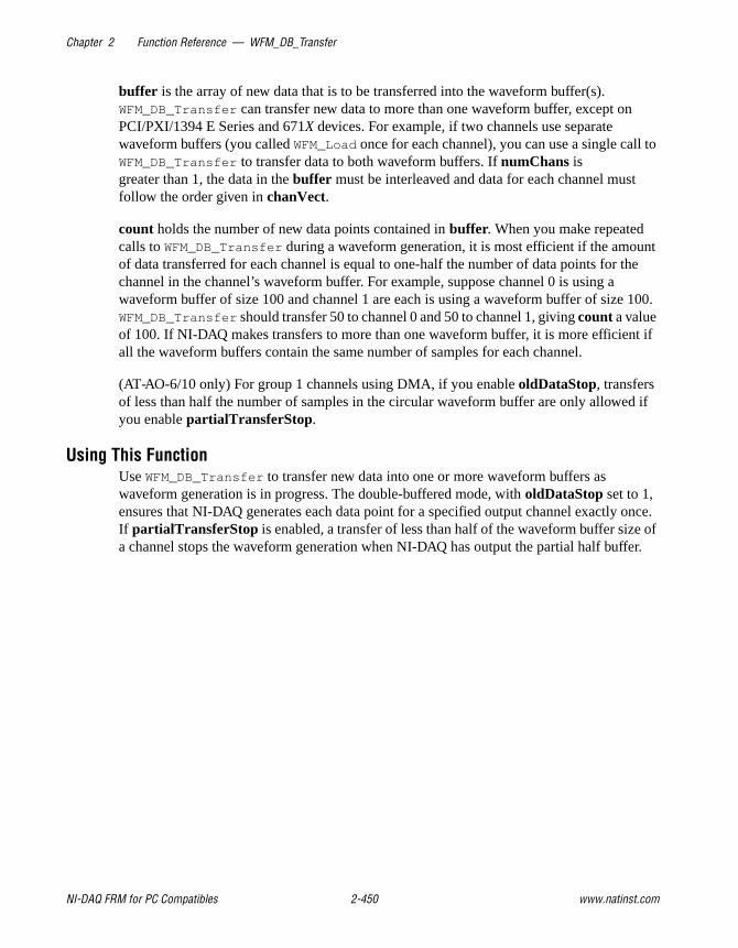
Chapter 2 Function Reference — WFM_DB_Transfer
NI-DAQ FRM for PC Compatibles 2-450 www.natinst.com
buffer is the array of new data that is to be transferred into the waveform buffer(s). WFM_DB_Transfer can transfer new data to more than one waveform buffer, except on PCI/PXI/1394 E Series and 671X devices. For example, if two channels use separate waveform buffers (you called WFM_Load once for each channel), you can use a single call to WFM_DB_Transfer to transfer data to both waveform buffers. If numChans is greater than 1, the data in the buffer must be interleaved and data for each channel must follow the order given in chanVect.
count holds the number of new data points contained in buffer. When you make repeated calls to WFM_DB_Transfer during a waveform generation, it is most efficient if the amount of data transferred for each channel is equal to one-half the number of data points for the channel in the channel’s waveform buffer. For example, suppose channel 0 is using a waveform buffer of size 100 and channel 1 are each is using a waveform buffer of size 100. WFM_DB_Transfer should transfer 50 to channel 0 and 50 to channel 1, giving count a value of 100. If NI-DAQ makes transfers to more than one waveform buffer, it is more efficient if all the waveform buffers contain the same number of samples for each channel.
(AT-AO-6/10 only) For group 1 channels using DMA, if you enable oldDataStop, transfers of less than half the number of samples in the circular waveform buffer are only allowed if you enable partialTransferStop .
Using This FunctionUse WFM_DB_Transfer to transfer new data into one or more waveform buffers as waveform generation is in progress. The double-buffered mode, with oldDataStop set to 1, ensures that NI-DAQ generates each data point for a specified output channel exactly once. If partialTransferStop is enabled, a transfer of less than half of the waveform buffer size of a channel stops the waveform generation when NI-DAQ has output the partial half buffer.

Chapter 2 Function Reference — WFM_from_Disk
© National Instruments Corporation 2-451 NI-DAQ FRM for PC Compatibles
WFM_from_Disk
Formatstatus = WFM_from_Disk (deviceNumber, numChans, chanVect, fileName, startPt, endPt,
iterations, rate)
PurposeAssigns a disk file to one or more analog output channels, selects the rate and the number of times the data in the file is to be generated, and starts the generation. This function always waits for completion before returning, unless you call Timeout_Config .
ParametersInput
Parameter DiscussionnumChans indicates the number of analog output channels specified in the array chanVect.
chanVect is the array of channel numbers indicating which analog output channels are to receive output data from the file.Channel number range:
0 or 1 for most devices.0 through 3 for PCI-6711.0 through 5 for AT-AO-6.0 through 7 for PCI-6713.0 through 9 for AT-AO-10.
Name Type Description
deviceNumber i16 assigned by configuration utility
numChans i16 number of analog output channels
chanVect [i16] channel numbers
fileName STR name of the data file containing the waveform data
startPt u32 place in a file where waveform generation is to begin
endPt u32 place in a file where waveform generation is to end
iterations u32 number of times generated
rate f64 desired rate in points per second

Chapter 2 Function Reference — WFM_from_Disk
NI-DAQ FRM for PC Compatibles 2-452 www.natinst.com
fileName is the name of the data file containing the waveform data. For MIO devices (except 6052E devices, PCI-MIO-16XE-10, and VXI-MIO-64XE-10), AT-AO-6/10, and Lab and 1200 Series analog output devices, the file must contain integer data ranging from 0 to 4,095 for unipolar mode and from –2,048 to 2,047 for bipolar mode. For 6052E devices and PCI-MIO-16XE-10, the file must contain integer data ranging from 0 to 65,535 for unipolar mode, and from –32,768 to +32,767 for bipolar mode.
For DSA devices, the file must contain integer data ranging from –131,072 to +131,071. Each data point is 32 bits wide but only the most significant 18 bits are used. The lower 14 bits are ignored and should be zero. You can move each data point into the upper 18 bits with a left shift operation or by multiplying it by 16,384.
startPt is the place in a file where waveform generation is to begin.Range: 1 through the number of samples in the file.
endPt is the place in a file where waveform generation is to end. A value of 0 for endPt has a special meaning. When endPt equals 0, waveform generation proceeds to the end of the file and wrap around to startPt if iterations is greater than 1.Range: 1 through the number of samples in the file.
iterations is the number of times the data in the file is generated.Range: 1 through 232 – 1.
rate is the rate of waveform generation you want in points per second (pts/s). A value of 0.0 for rate means that external update pulses (applied to EXTUPDATE for the AT-AO-6/10 and Lab and 1200 Series analog output devices) determine the waveform generation rate. If you are using an E Series or 671X device, see the Select_Signal function for information about the external timing signals.Range: 0.0 for external update or approximately 0.0015 to 500,000 pts/s. Your maximum
rate depends on your device type and your computer system.
If the number of points that represent one cycle of the waveform equals count, the frequency of the generated waveform is related to the rate by this the following formula:
frequency = (rate/count) cycles per second
Using This FunctionWFM_from_Disk initiates a waveform generation operation. NI-DAQ writes the portion of data in the file determined by startPt and endPt to the specified analog output channels at a rate as close to the rate you want as the hardware permits (see WFM_Rate for further explanation). If numChans is greater than 1, NI-DAQ writes the data values from file to the DAC in ascending order. WFM_from_Disk always waits until the requested number of file iterations is complete before returning.

Chapter 2 Function Reference — WFM_from_Disk
© National Instruments Corporation 2-453 NI-DAQ FRM for PC Compatibles
If you have changed the analog output configuration from the defaults by changing the jumpers on the device, you must call AO_Configure to set the software copies of the settings prior to calling WFM_from_Disk .
NI-DAQ ignores the group settings made by calling WFM_Group_Setup when you call WFM_from_Disk . WFM_from_Disk and the settings are not changed after you execute WFM_from_Disk .
For Lab and 1200 Series analog output devices, if the rate is smaller than 15.26 pts/s and counter B0 is busy in a data acquisition or counting operation, waveform generation cannot proceed.
On Am9513-based devices, to externally trigger a waveform generation operation, you can do so by first changing the gating mode of the counter NI-DAQ uses.
WFM_from_Disk uses either the default gating mode (none) or the gating mode you specify through the CTR_Config function. You need to connect your trigger signal to the gate pin on the I/O connector. Refer to the CTR_Config function description for details.
On a variety of E Series or 671X devices, you can externally trigger a waveform generation in a variety of ways. Refer to the Select_Signal function for more details.

Chapter 2 Function Reference — WFM_Group_Control
NI-DAQ FRM for PC Compatibles 2-454 www.natinst.com
WFM_Group_Control
Formatstatus = WFM_Group_Control (deviceNumber, group, operation)
PurposeControls waveform generation for a group of analog output channels.
ParametersInput
Parameter Discussiongroup is the group of analog output channels (see WFM_Group_Setup).Range: 1 for most devices.
1 or 2 for the AT-AO-6/10.
operation selects the operation NI-DAQ is to perform for the group of output channels.operation = 0 (CLEAR): Terminates a waveform operation for the group of analog output
channels. The last voltage produced at the DAC is maintained indefinitely. After you execute CLEAR for an analog output group, you must call WFM_Load before you can restart waveform generation using operation = START.
operation = 1 (START): Initiates waveform generation at the analog output channels in group. Your application must call operation = CLEAR before terminating, if START is executed. If you do not execute CLEAR, unpredictable behavior might result.
Note If you invoke this function to clear continuous waveform generation that was stopped previously because of an underflow error, WFM_Group_Control does not report the occurrence of the underflow error. If you want to check for this type of error, invoke function WFM_Check prior to invoking WFM_Group_Control to clear waveform generation.
Name Type Description
deviceNumber i16 assigned by configuration utility
group i16 group of analog output channels
operation i16 operation to be performed

Chapter 2 Function Reference — WFM_Group_Control
© National Instruments Corporation 2-455 NI-DAQ FRM for PC Compatibles
Note For Lab and 1200 Series analog output devices, if the rate is smaller than 15.26 pts/s and counter B0 is busy in a data acquisition operation, waveform generation cannot proceed.
operation = 2 (PAUSE): Temporarily halts waveform generation for the group of channels. NI-DAQ maintains the last voltage written to the DAC indefinitely.
Note This value of operation = 2 is not supported for the AT bus E Series devices (except the AT-MIO-16XE-10), the PCI-4451, the NI 4551, or the PCI-4453.
operation = 4 (RESUME): Restarts waveform generation for the group of channels that previously halted by operation = PAUSE.
Note This value of operation = 4 is not supported for the AT bus E Series devices (except the AT-MIO-16XE-10), the PCI-4451, the NI 4551, or the PCI-4453.
When you have halted a waveform generation by executing PAUSE, RESUME restarts the waveform exactly at the point in your buffer where it left off. If n iterations of the buffer remained to be completed when you executed operation = PAUSE, those n iterations are generated after NI-DAQ executes RESUME. RESUME restarts waveform generation if NI-DAQ has completed the number of iterations specified in WFM_Load.

Chapter 2 Function Reference — WFM_Group_Setup
NI-DAQ FRM for PC Compatibles 2-456 www.natinst.com
WFM_Group_Setup
Formatstatus = WFM_Group_Setup (deviceNumber, numChans, chanVect, group)
PurposeAssigns one or more analog output channels to a waveform generation group. A call to WFM_Group_Setup is only required for the AT-AO-6/10. By default, both analog output channels for the MIO devices and the Lab-PC+ are in group 1.
ParametersInput
Parameter DiscussionnumChans indicates the number of analog output channels specified in the array chanVect. A 0 clears the channel assignments for group.Range: 0 through 2 for most devices.
0 through 4 for PCI-6711.0 through 6 for AT-AO-6.0 through 8 for PCI-6713.0 through 10 for AT-AO-10.
chanVect is your array of channel numbers indicating which analog output channels are in a group.Channel number range:
0 or 1 for most devices.0 through 5 for AT-AO-6.0 through 9 for AT-AO-10.0 through 3 for PCI-6711.0 through 7 for PCI-6713.
group is the group number.Range: 1 for most devices.
1 or 2 for AT-AO-6/10.
Name Type Description
deviceNumber i16 assigned by configuration utility
numChans i16 number of analog output channels
chanVect [i16] channel numbers
group i16 group number

Chapter 2 Function Reference — WFM_Group_Setup
© National Instruments Corporation 2-457 NI-DAQ FRM for PC Compatibles
Using This FunctionFor the AT-AO-6/10, you can assign analog output channels to one of two waveform generation groups. Each group has a separate update clock source. You can assign different update rates to each group by calling WFM_ClockRate .
Rules for This FunctionYou cannot split channel pairs between groups (channel pairs are 0 and 1, 2 and 3, 4 and 5, and so on) for the AT-AO-6/10. For example, you can assign channel 4 alone to group 1, but you cannot then assign channel 5 to group 2.
The rules for the AT-AO-6 group 1 assignments are as follows:
• 0 to n, where n ≤ 5 and the channel list is consecutive, or any one channel.
• Use interrupts/DMA with FIFO.
• Interrupt when the FIFO is half full; thus, group 1 will be faster than group 2, even when interrupts are used for both.
• If more than one channel is in the channel list, then channel 0 must be the first channel in that list.
The rules for AT-AO-6 group 2 assignments are as follows:
• Channels 0 or 1 cannot be in group 2.
• Uses interrupts only.
The rules for AT-AO-10 group assignments are as follows:
• All rules of assignment for the AT-AO-6 apply to the AT-AO-10.
• 0 to n, where n ≤ 9 and the channel list is consecutive, or any one channel.
• If exactly one channel is assigned to group 1, it cannot be channel 8 or 9.

Chapter 2 Function Reference — WFM_Load
NI-DAQ FRM for PC Compatibles 2-458 www.natinst.com
WFM_Load
Formatstatus = WFM_Load (deviceNumber, numChans, chanVect, buffer, count, iterations, mode)
PurposeAssigns a waveform buffer to one or more analog output channels and indicates the number of waveform cycles to generate.
ParametersInput
Parameter DiscussionnumChans indicates the number of analog output channels specified in the array chanVect.Range: 1 or 2 for most devices.
1 through 4 for PCI-6711.1 through 6 for AT-AO-6.1 through 8 for PCI-6713.1 through 10 for AT-AO-10.
chanVect is the array of channel numbers indicating to which analog output channels the buffer to be assigned.Channel number range:
0 or 1 for most devices.0 through 5 for AT-AO-6.0 through 9 for AT-AO-10.0 through 3 for PCI-6711.0 through 7 for PCI-6713.
Name Type Description
deviceNumber i16 assigned by configuration utility
numChans i16 number of analog output channels
chanVect [i16] channel numbers
buffer [i16] values that are converted to voltages by DACs
count u32 number of points in the buffer
iterations u32 number of times the waveform generation steps through buffer
mode i16 enables or disables FIFO mode

Chapter 2 Function Reference — WFM_Load
© National Instruments Corporation 2-459 NI-DAQ FRM for PC Compatibles
buffer is an array of integer values that are converted to voltages by DACs. If your device has 12-bit DACs, the data ranges from 0 to 4,095 in unipolar mode and from –2,048 to 2,047 in bipolar mode. If your device has 16-bit DACs, the data ranges from 0 to 65,535 in unipolar mode and from –32,768 to +32,767 in bipolar mode.
Note For all devices except the National Instruments devices, data points for the output channels need to be interleaved when you set up the buffer parameter.
The DSA devices have 18-bit DACs and operate only in bipolar mode. Data ranges from –131,072 to +131,071. For DSA devices each buffer element is 32 bits wide. Each data point goes in the upper 18 bits of its buffer element. You should set the lower 14 bits to 0.You can move each data point into the upper 18 bits with a left shift operation or by multiplying it by 16,384.
count is the number of points in your buffer. When you use interleaved waveform generation, count should be a multiple of numChans and not less than 2 * numChans. When you use double-buffered interleaved waveform generation, count should not be less than 4 * numChans.Range: 1 through 232 –1 (most devices).
2 through 224 (E Series, 671X devices, PCI-4451, and PCI-4453).
On the PCI-61XX and 671X devices, the buffer must contain an even number of samples because of the 32-bit FIFO.
iterations is the number of times the waveform generation steps through buffer. A value of 0 means that waveform generation proceeds indefinitely.Range: 0 through 232 – 1.
Enabling FIFO mode waveform generation places some restrictions on the allowable values for the iterations parameter. Refer to the mode parameter description below.
Enabling pulsed FIFO mode waveform generation by turning on the delay clock via WFM_ClockRate places two additional restrictions on the allowed values of iterations and also changes its meaning. Setting iterations to 0 is not allowed. Also, instead of determining the number of times the waveform generation steps through buffer before stopping, pulsed FIFO mode causes the iterations setting to determine the number of times the data in the FIFO is generated before pausing for the specified delay. Once the delay has elapsed, the data in the FIFO is generated again. In other words, when you use pulsed FIFO mode, the value of iterations determines the number of cycles through the FIFO that occurs between delays, and the pattern of waveform followed by delay is followed by waveform and so on, which goes on indefinitely.

Chapter 2 Function Reference — WFM_Load
NI-DAQ FRM for PC Compatibles 2-460 www.natinst.com
mode allows you to indicate whether to use FIFO mode waveform generation, if your device has a FIFO.Range: 0 or 1 for most devices.
0 for all other devices.1, 2, 3, or 4 for the NI 5411 devices.
Note To determine the size of the analog output FIFO on your board, refer to your hardware manual.
When mode is 0, NI-DAQ does not use FIFO mode waveform generation. When mode is 1 and all of the following conditions are satisfied, NI-DAQ uses FIFO mode waveform generation:
• The waveform buffer is small enough to reside in the DAC FIFO. If you load more than one channel, the total number of points must be less than or equal to the FIFO size.
• You have not enabled double-buffered waveform generation mode.
• For the AT-AO-6/10, iterations must be 0.
• All the channels listed in chanVect must belong to group 1.
• If more than one channel of group 1 is loaded, the number of points per channel and iterations are the same for each channel. Also, all the channels of group 1 must have the same mode.
NI-DAQ returns error fifoModeError if any of the previously described conditions is not satisfied and mode is 1. If you call the WFM_Load function several times to load different channels, the WFM_Group_Control function checks for conditions 1 and 5.
Note On PCI/PXI/CPCI/1394 E Series and 671X devices, you cannot load multiple buffers for a single group.
When mode is 1 and you have enabled the delay clock (see the WFM_ClockRate function), the waveform generation proceeds until it is stopped by software. In this case, iterations indicates how many times the waveform is generated between delays.
Using This FunctionWFM_Load assigns your buffer to a selected analog output channel or channels. The values in this buffer are translated to voltages by the D/A circuitry and produced at the output channel when you have called WFM_Group_Control (operation = START) for a channel group. To change the shape of a waveform in progress, use WFM_DB_Config to enable double-buffered mode and WFM_DB_Transfer to transfer data into the waveform buffer. When loading buffers for double-buffered mode, all of the channel buffers should be the same size.

Chapter 2 Function Reference — WFM_Load
© National Instruments Corporation 2-461 NI-DAQ FRM for PC Compatibles
WFM_Load assigns your buffer to a selected analog output channel or channels. The values in this buffer are translated to voltages by the digital-to-analog (D/A) circuitry and produced at the output channel when you have called WFM_Group_Control (operation = START) for a channel group. If you have changed the analog output configuration from the defaults by changing the jumpers on the device, you must call AO_Configure to set the software copies of the settings prior to calling WFM_Group_Control (operation = START). You can make repeated calls to WFM_Load to change the shape of a waveform in progress, except on E Series devices and SCXI DAQ modules used with remote SCXI; if you make repeated calls using these devices, this function will return a transferInProgError . You also must use the parameter values for numChans and chanVect used in the call to WFM_Load prior to starting the waveform when making calls to WFM_Load while a waveform is in progress.
The DSA devices use 32-bit data buffers. If you are using C or Delphi, you will need to type cast your i32 array to i16 when you call WFM_Load. If you are using Visual Basic, you should use the nidaqr32.bas file (instead of nidaq32.bas ) to relax type checking on buffer. The DSA devices use the upper 18 bits of each buffer element. The lower 14 bits are ignored and you should set them to 0.

Chapter 2 Function Reference — WFM_Op
NI-DAQ FRM for PC Compatibles 2-462 www.natinst.com
WFM_Op
Formatstatus = WFM_Op (deviceNumber, numChans, chanVect, buffer, count, iterations, rate)
PurposeAssigns a waveform buffer to one or more analog output channels, selects the rate and the number of times the data in the buffer is to be generated, and starts the generation. If the number of buffer generations is finite, WFM_Op waits for completion before returning, unless you call Timeout_Config .
ParametersInput
Parameter DiscussionnumChans indicates the number of analog output channels specified in the array chanVect.
chanVect is the array of channel numbers indicating which analog output channels are to receive output data from the buffer.Channel number range:
0 or 1 for most devices.0 through 5 for AT-AO-6.0 through 9 for AT-AO-10.0 through 3 for PCI-6711.0 through 7 for PCI-6713.
Name Type Description
deviceNumber i16 assigned by configuration utility
numChans i16 number of analog output channels
chanVect [i16] channel numbers
buffer [i16] values that are converted to voltages by DACs
count u32 number of points in the buffer
iterations u32 number of times the waveform generation steps through buffer
rate f64 desired rate in points per second

Chapter 2 Function Reference — WFM_Op
© National Instruments Corporation 2-463 NI-DAQ FRM for PC Compatibles
buffer is an array of integer values that DACs convert to voltages. If your device has 12-bit DACs, data ranges from 0 to 4,095 in unipolar mode and from –2,048 to 2,047 in bipolar mode. If your device has 16-bit DACs, data ranges from 0 to 65,535 in unipolar mode and from –32,768 to +32,767 in bipolar mode.
The DSA devices have 18-bit DACs and operate in bipolar mode only. Data ranges from –131,072 to +131,071. For DSA devices each buffer element is 32 bits wide. Each data point goes in the upper 18 bits of its buffer element. You should set the lower bits to zero.
count is the number of points in your buffer. When NI-DAQ is using interleaved waveform generation, count should be a multiple of numChans and not less than 2 * numChans. Range: 1 through 232 – 1 (except E Series devices).
2 through 224 (E Series and 671X devices).
On PCI-61XX and 671X devices, the buffer must contain an even number of samples because of the 32-bit FIFO.
iterations is the number of times the waveform generation steps through buffer. A value of 0 means that waveform generation proceeds indefinitely.Range: 0 through 232 – 1.
rate is the rate of waveform generation you want in points per second (pts/s). A value of 0.0 for rate means that external update pulses (applied to EXTUPDATE for the AT-AO-6/10 and Lab and 1200 Series analog output devices, and to PFI Pin 5 on E Series and 671X devices) will determine the waveform generation rate.Range: 0.0 for external update or approximately 0.0015 to 500,000 pts/s.
Your maximum rate depends on your device type and your computer system. If the number of points that represents represent one cycle of the waveform equals count, the frequency of the generated waveform is related to the rate by this the following formula:
frequency = (rate/count) cycles per second
Using This FunctionWFM_Op initiates a waveform generation operation. NI-DAQ writes the data in the buffer to the specified analog output channels at a rate as close to the rate you want as the specified rate hardware permits (see WFM_Rate for a further explanation). With the exception of indefinite waveform generation, WFM_Op waits until NI-DAQ completes the waveform generation is complete before returning (that is, it is synchronous).
If you have changed the analog output configuration from the defaults by changing the jumpers on the device, you must call AO_Configure to set the software copies of the settings prior to calling WFM_Op.
NI-DAQ ignores the group settings made by calling WFM_Group_Setup when you call WFM_Op and the settings are not changed after NI-DAQ executes you execute WFM_Op.

Chapter 2 Function Reference — WFM_Op
NI-DAQ FRM for PC Compatibles 2-464 www.natinst.com
For Lab and 1200 Series analog output devices, if the rate is smaller than 15.26 pts/s and counter B0 is busy in a data acquisition or counting operation, waveform generation cannot proceed.
WFM_OP uses either the default gating mode (none) or the gating mode you specify through the CTR_Config function. You need to connect your trigger signal to the gate pin on the I/O connector. Refer to the CTR_Config function description for details.
On E Series and 671X devices, you can externally trigger a waveform generation operation in a variety of ways. Refer to the Select_Signal function for more details.
The DSA devices use 32-bit data buffers. If you are using C or Delphi, you need to typecast your i32 array to i16 when you call WFM_Op. If you are using Visual Basic, you should use the nidaqr32.bas file (instead of nidaq32.bas ) to relax type checking on buffer. The DSA devices use the upper 18 bits of each buffer element. The lower 14 bits are ignored and you should set them to 0. You can move each data point into the upper 18 bits with a left shift operation by multiplying it by 16,384.

Chapter 2 Function Reference — WFM_Rate
© National Instruments Corporation 2-465 NI-DAQ FRM for PC Compatibles
WFM_Rate
Formatstatus = WFM_Rate (rate, units, timebase, updateInterval)
PurposeConverts a waveform generation update rate into the timebase and update-interval values needed to produce the rate you want.
ParametersInput
Output
Parameter Discussionrate is the waveform generation update rate you want. rate is expressed in either pts/s or seconds per point (s/pt), depending on the value of the units parameter.Range: Roughly 0.00153 pts/s through 500,000 pts/s or 655 s/pt through 0.000002 s/pt.
units indicates the units used to express rate.0: points per second.1: seconds per point.
timebase is a code representing the resolution of the onboard clock signal that the device uses to produce the update rate you want. You can input the value returned in timebase directly to WFM_ClockRate . timebase has the following possible values:
–3: 20 MHz clock used as a timebase (50 ms) (E Series and 671X devices only).–1: 5 MHz clock used as timebase (200 ns resolution).1: 1 MHz clock used as timebase (1 µs resolution).2: 100 kHz clock used as timebase (10 µs resolution).3: 10 kHz clock used as timebase (100 µs resolution).
Name Type Description
rate f64 update rate you want
units i16 units used
Name Type Description
timebase *i16 resolution of clock signal
updateInterval *u32 number of timebase units

Chapter 2 Function Reference — WFM_Rate
NI-DAQ FRM for PC Compatibles 2-466 www.natinst.com
4: 1 kHz clock used as timebase (1 ms resolution).5: 100 Hz clock used as timebase (10 ms resolution).
updateInterval is the number of timebase units that elapse between consecutive writes (updates) to the D/A converters. The combination of the timebase resolution value and the updateInterval produces the waveform generation rate you want. You can input the value returned in updateInterval directly to WFM_ClockRate . Range: 2 through 65,535.
Note If you are using an SCXI-1200 with remote SCXI, the maximum rate depends on the baud rate setting and updateRate. Refer to the SCXI-1200 User Manual for more details.
Note C Programmers—timebase and updateInterval are pass-by-address parameters.
Using This FunctionWFM_Rate produces timebase and updateInterval values to closely match the update rate you want. To calculate the actual rate produced by these values, first determine the clock resolution that corresponds to the value timebase returns. Then use the appropriate formula below, depending on the value specified for units:
units = 0 (pts/s).
actual rate = 1/(clock resolution * updateInterval).
units = 1 (s/pt).
actual rate = clock resolution * updateInterval.

Chapter 2 Function Reference — WFM_Scale
© National Instruments Corporation 2-467 NI-DAQ FRM for PC Compatibles
WFM_Scale
Formatstatus = WFM_Scale (deviceNumber, chan, count, gain, voltArray, binArray)
PurposeTranslates an array of floating-point values that represent voltages into an array of binary values that produce those voltages when NI-DAQ writes the binary array to one of the board DACs. This function uses the current analog output configuration settings to perform the conversions.
ParametersInput
Output
Parameter Discussionchan indicates to which analog output channel the binary array is to be assigned.Range: 0 or 1 for most devices.
0 through 5 for AT-AO-6.0 through 9 for AT-AO-10.0 through 3 for PCI-6711.0 through 7 for PCI-6713.
count is the number of points in your buffer.Range:1 through 232 – 1.
Name Type Description
deviceNumber i16 assigned by configuration utility
chan i16 analog output channel
count u32 number of points in the buffer
gain f64 multiplier applied as the translation is performed
voltArray [f64] input double-precision values
Name Type Description
binArray [i16] binary values converted from the voltages

Chapter 2 Function Reference — WFM_Scale
NI-DAQ FRM for PC Compatibles 2-468 www.natinst.com
gain is a multiplier applied to the array as NI-DAQ performs the translation. If the result of multiplying each element in the array by the value of gain produces a voltage that is out of range, NI-DAQ sets the voltage to the maximum or minimum value and returns an error. NI-DAQ still completes the translation, however.Range: Any real number that produces a voltage within the analog output range.
voltArray is the input array of double-precision values that represents the voltages NI-DAQ is to produce at one of the outputs.Range: Any real number that produces a voltage within the analog output range.
binArray is the array of binary values converted from the voltages contained in voltArray . The values in binArray produce the original voltages when NI-DAQ writes them to a DAC on your device. Refer to Appendix B, Analog Input Channel, Gain Settings, and Voltage Calculation, for the calculation of binary value.
Using This FunctionWFM_Scale calculates each binary value using the following formulas:
• Unipolar configuration:
12-bit DACs: binVal = voltage * (gain * (4096/outputRange)).
16-bit DACs: binVal = voltage * (gain * (65536/outputRange)).
• Bipolar configuration:
12-bit DACs: binVal = voltage * (gain * (2048/outputRange)).
16-bit DACs: binVal = voltage * (gain * (32768/outputRange)).
18-bit DACs: binVal = voltage * (gain * (131072/outputRange)).
The DSA devices use 32-bit data buffers. If you are using C or Delphi, you need to typecast your i32 array to i16 when you call WFM_Scale. If you are using Visual Basic, you should use the nidaqr32.bas file (instead of nidaq32.bas ) to relax type checking on binArray . Each 18-bit binVal is shifted into the upper 18 bits of the array element.

Chapter 2 Function Reference — WFM_Set_Clock
© National Instruments Corporation 2-469 NI-DAQ FRM for PC Compatibles
WFM_Set_Clock
Formatstatus = WFM_Set_Clock (deviceNumber, group, whichClock, desiredRate, units, actualRate)
PurposeSets the update rate for a group of channels (DSA devices only).
ParametersInput
Output
Parameter Discussiongroup is the group of analog output channels (see WFM_Group_Setup) .Range: 1.
whichClock indicates the type of clock. Only one clock is currently supported so set this parameter to zero.
desiredRate is the rate at which you want data points to be sent to the DACs.
units determines how desiredRate and actualRate are interpreted: 0: points per second.1: seconds per point.
Name Type Description
deviceNumber i16 assigned by configuration utility
group i16 group of analog output channels
whichClock u32 only update clock supported
desiredRate f64 desired update rate in units
units u32 ticks per second or seconds per tick
Name Type Description
actualRate *f64 actual update rate in units

Chapter 2 Function Reference — WFM_Set_Clock
NI-DAQ FRM for PC Compatibles 2-470 www.natinst.com
actualRate is the rate at which data points are sent to the DACs. The capabilities of your device determine how closely actualRate matches desiredRate. The DSA devices use the same base clock for both DAQ/SCAN and WFM operations so the rates available for WFM are restricted if a DAQ/SCAN operation is already in progress.
Note C Programmers—actualRate is a pass-by-address parameter.
Using This FunctionThe frequency of a waveform is related to the update rate and the number of points in the buffer (indicated in an earlier call to WFM_Load). Assuming that your buffer contains exactly one period of your waveform:
frequency = update rate/points in the buffer
You can make repeated calls to WFM_Set_Clock to change the update rate of a waveform in progress.

© National Instruments Corporation A-1 NI-DAQ FRM for PC Compatibles
AError Codes
This appendix lists the error codes returned by NI-DAQ, including the name and description.
Each NI-DAQ function returns a status code that indicates whether the function was performed successfully. When an NI-DAQ function returns a code that is a negative number, it means that the function did not execute. When a positive status code is returned, it means that the function did execute, but with a potentially serious side effect. A summary of the error codes is listed in Table A-1.
Note All error codes and descriptions are also listed in the NI-DAQ online help.
Table A-1. Error Code Summary
Error Code Error Name Description
–10001 syntaxError An error was detected in the input string; the arrangement or ordering of the characters in the string is not consistent with the expected ordering.
–10002 semanticsError An error was detected in the input string; the syntax of the string is correct, but certain values specified in the string are inconsistent with other values specified in the string.
–10003 invalidValueError The value of a numeric parameter is invalid.
–10004 valueConflictError The value of a numeric parameter is inconsistent with another one, and therefore the combination is invalid.
–10005 badDeviceError The device is invalid.
–10006 badLineError The line is invalid.

Appendix A Error Codes
NI-DAQ FRM for PC Compatibles A-2 www.natinst.com
–10007 badChanError A channel, port, or counter is out of range for the device type or device configuration; or the combination of channels is not allowed; or the scan order must be reversed (0 last).
–10008 badGroupError The group is invalid.
–10009 badCounterError The counter is invalid.
–10010 badCountError The count is too small or too large for the specified counter, or the given I/O transfer count is not appropriate for the current buffer or channel configuration.
–10011 badIntervalError The analog input scan rate is too fast for the number of channels and the channel clock rate; or the given clock rate is not supported by the associated counter channel or I/O channel.
–10012 badRangeError The analog input or analog output voltage range is invalid for the specified channel, or you are writing an invalid voltage to the analog output.
–10013 badErrorCodeError The driver returned an unrecognized or unlisted error code.
–10014 groupTooLargeError The group size is too large for the board.
–10015 badTimeLimitError The time limit is invalid.
–10016 badReadCountError The read count is invalid.
–10017 badReadModeError The read mode is invalid.
–10018 badReadOffsetError The offset is unreachable.
–10019 badClkFrequencyError The frequency is invalid.
–10020 badTimebaseError The timebase is invalid.
–10021 badLimitsError The limits are beyond the range of the board.
Table A-1. Error Code Summary (Continued)
Error Code Error Name Description

Appendix A Error Codes
© National Instruments Corporation A-3 NI-DAQ FRM for PC Compatibles
–10022 badWriteCountError Your data array contains an incomplete update, or you are trying to write past the end of the internal buffer, or your output operation is continuous and the length of your array is not a multiple of one half of the internal buffer size.
–10023 badWriteModeError The write mode is out of range or is not allowed.
–10024 badWriteOffsetError Adding the write offset to the write mark places the write mark outside the internal buffer.
–10025 limitsOutOfRangeError The requested input limits exceed the board's capability or configuration. Alternative limits were selected.
–10026 badBufferSpecificationError The requested number of buffers or the buffer size is not allowed. For example, the buffer limit for Lab and 1200 devices is 64K samples, or the board does not support multiple buffers.
–10027 badDAQEventError For DAQEvents 0 and 1 general value A must be greater than 0 and less than the internal buffer size. If DMA is used for DAQEvent 1, general value A must divide the internal buffer size evenly, with no remainder. If the TIO-10 is used for DAQEvent 4, general value A must be 1 or 2.
–10028 badFilterCutoffError The cutoff frequency specified is not valid for this device.
–10029 obsoleteFunctionError The function you are calling is no longer supported in this version of the driver.
–10030 badBaudRateError The specified baud rate for communicating with the serial port is not valid on this platform.
Table A-1. Error Code Summary (Continued)
Error Code Error Name Description

Appendix A Error Codes
NI-DAQ FRM for PC Compatibles A-4 www.natinst.com
–10031 badChassisIDError The specified SCXI chassis does not correspond to a configured SCXI chassis.
–10032 badModuleSlotError The SCXI module slot that was specified is invalid or corresponds to an empty slot.
–10033 invalidWinHandleError The window handle passed to the function is invalid.
–10034 noSuchMessageError No configured message matches the one you tried to delete.
–10035 irrelevantAttributeError The specified attribute is not relevant.
–10036 badYearError The specified year is invalid.
–10037 badMonthError The specified month is invalid.
–10038 badDayError The specified day is invalid.
–10039 stringTooLongError The specified input string is too long. For instance, DAQScope 5102 devices can only store a string upto 32 bytes in length on the calibration EEPROM. In that case, shorten the string.
–10040 badGroupSizeError The group size is invalid.
–10041 badTaskIDError The specified task ID is invalid. For instance, you may have connected a taskID from an Analog Input VI to a Digital I/O VI.
–10042 inappropriateControlCodeError The specified control code is inappropriate for the current configuration or state.
–10043 badDivisorError The specified divisor is invalid.
–10044 badPolarityError The specified polarity is invalid.
–10045 badInputModeError The specified input mode is invalid.
–10079 badTrigSkipCountError The trigger skip count is invalid.
–10080 badGainError The gain or gain adjust is invalid.
Table A-1. Error Code Summary (Continued)
Error Code Error Name Description

Appendix A Error Codes
© National Instruments Corporation A-5 NI-DAQ FRM for PC Compatibles
–10081 badPretrigCountError The pretrigger sample count is invalid.
–10082 badPosttrigCountError The posttrigger sample count is invalid.
–10083 badTrigModeError The trigger mode is invalid.
–10084 badTrigCountError The trigger count is invalid.
–10085 badTrigRangeError The trigger range or trigger hysteresis window is invalid.
–10086 badExtRefError The external reference is invalid.
–10087 badTrigTypeError The trigger type is invalid.
–10088 badTrigLevelError The trigger level is invalid.
–10089 badTotalCountError The total count is inconsistent with the buffer size and pretrigger scan count or with the board type.
–10090 badRPGError The individual range, polarity, and gain settings are valid but the combination is not allowed.
–10091 badIterationsError You have attempted to use an invalid setting for the iterations parameter. The iterations value must be 0 or greater. Your device might be limited to only two values, 0 and 1.
–10092 lowScanIntervalError Some devices require a time gap between the last sample in a scan and the start of the next scan. The scan interval you have specified does not provide a large enough gap for the board. See your documentation for an explanation.
–10093 fifoModeError FIFO mode waveform generation cannot be used because at least one condition is not satisfied.
–10094 badCalDACconstError The calDAC constant passed to the function is invalid.
Table A-1. Error Code Summary (Continued)
Error Code Error Name Description

Appendix A Error Codes
NI-DAQ FRM for PC Compatibles A-6 www.natinst.com
–10095 badCalStimulusError The calibration stimulus passed to the function is invalid.
–10096 badCalibrationConstantError The specified calibration constant is invalid.
–10097 badCalOpError The specified calibration operation is invalid.
–10098 badCalConstAreaError The specified calibration constant area is invalid. For instance, the specified calibration constant area contains constants which cannot be modified outside the factory.
–10100 badPortWidthError The requested digital port width is not a multiple of the hardware port width or is not attainable by the DAQ hardware.
–10120 gpctrBadApplicationError Invalid application used.
–10121 gpctrBadCtrNumberError Invalid counterNumber used.
–10122 gpctrBadParamValueError Invalid paramValue used.
–10123 gpctrBadParamIDError Invalid paramID used.
–10124 gpctrBadEntityIDError Invalid entityID used.
–10125 gpctrBadActionError Invalid action used.
–10126 gpctrSourceSelectError Invalid source selected.
–10127 badCountDirError The specified counter does not support the specified count direction.
–10128 badGateOptionError The specified gating option is invalid.
–10129 badGateModeError The specified gate mode is invalid.
–10130 badGateSourceError The specified gate source is invalid.
–10131 badGateSignalError The specified gate signal is invalid.
–10132 badSourceEdgeError The specified source edge is invalid.
–10133 badOutputTypeError The specified output type is invalid.
Table A-1. Error Code Summary (Continued)
Error Code Error Name Description

Appendix A Error Codes
© National Instruments Corporation A-7 NI-DAQ FRM for PC Compatibles
–10134 badOutputPolarityError The specified output polarity is invalid.
–10135 badPulseModeError The specified pulse mode is invalid.
–10136 badDutyCycleError The specified duty cycle is invalid.
–10137 badPulsePeriodError The specified pulse period is invalid.
–10138 badPulseDelayError The specified pulse delay is invalid.
–10139 badPulseWidthError The specified pulse width is invalid.
–10140 badFOUTportError The specified frequency output (FOUT or FREQ_OUT) port is invalid.
–10141 badAutoIncrementModeError The specified autoincrement mode is invalid.
–10180 badNotchFilterError The specified notch filter is invalid.
–10181 badMeasModeError The specified measurement mode is invalid.
–10200 EEPROMreadError Unable to read data from EEPROM.
–10201 EEPROMwriteError Unable to write data to EEPROM.
–10202 EEPROMwriteProtectionError You cannot write into this location or area of your EEPROM because it is write-protected. You may be trying to store calibration constants into a write-protected area; if this is the case, you should select the user area of the EEPROM instead.
–10203 EEPROMinvalidLocationError The specified EEPROM location is invalid.
–10204 EEPROMinvalidPasswordError The password for accessing the EEPROM is incorrect.
–10240 noDriverError The driver interface could not locate or open the driver.
Table A-1. Error Code Summary (Continued)
Error Code Error Name Description

Appendix A Error Codes
NI-DAQ FRM for PC Compatibles A-8 www.natinst.com
–10241 oldDriverError One of the driver files or the configuration utility is out of date, or a particular feature of the Channel Wizard is not supported in this version of the driver.
–10242 functionNotFoundError The specified function is not located in the driver.
–10243 configFileError The driver could not locate or open the configuration file, or the format of the configuration file is not compatible with the currently installed driver.
–10244 deviceInitError The driver encountered a hardware-initialization error while attempting to configure the specified device.
–10245 osInitError The driver encountered an operating-system error while attempting to perform an operation, or the operating system does not support an operation performed by the driver.
–10246 communicationsError The driver is unable to communicate with the specified external device.
–10247 cmosConfigError The CMOS configuration-memory for the device is empty or invalid, or the configuration specified does not agree with the current configuration of the device, or the EISA system configuration is invalid.
–10248 dupAddressError The base addresses for two or more devices are the same; consequently, the driver is unable to access the specified device.
–10249 intConfigError The interrupt configuration is incorrect given the capabilities of the computer or device.
Table A-1. Error Code Summary (Continued)
Error Code Error Name Description
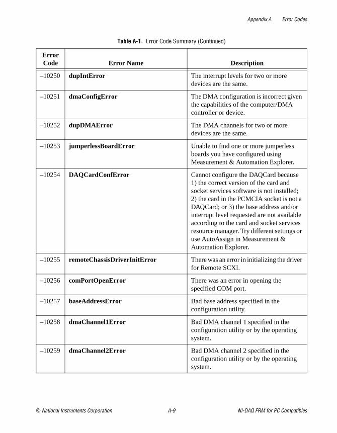
Appendix A Error Codes
© National Instruments Corporation A-9 NI-DAQ FRM for PC Compatibles
–10250 dupIntError The interrupt levels for two or more devices are the same.
–10251 dmaConfigError The DMA configuration is incorrect given the capabilities of the computer/DMA controller or device.
–10252 dupDMAError The DMA channels for two or more devices are the same.
–10253 jumperlessBoardError Unable to find one or more jumperless boards you have configured using Measurement & Automation Explorer.
–10254 DAQCardConfError Cannot configure the DAQCard because 1) the correct version of the card and socket services software is not installed; 2) the card in the PCMCIA socket is not a DAQCard; or 3) the base address and/or interrupt level requested are not available according to the card and socket services resource manager. Try different settings or use AutoAssign in Measurement & Automation Explorer.
–10255 remoteChassisDriverInitError There was an error in initializing the driver for Remote SCXI.
–10256 comPortOpenError There was an error in opening the specified COM port.
–10257 baseAddressError Bad base address specified in the configuration utility.
–10258 dmaChannel1Error Bad DMA channel 1 specified in the configuration utility or by the operating system.
–10259 dmaChannel2Error Bad DMA channel 2 specified in the configuration utility or by the operating system.
Table A-1. Error Code Summary (Continued)
Error Code Error Name Description

Appendix A Error Codes
NI-DAQ FRM for PC Compatibles A-10 www.natinst.com
–10260 dmaChannel3Error Bad DMA channel 3 specified in the configuration utility or by the operating system.
–10261 userModeToKernelModeCallError The user mode code failed when calling the kernel mode code.
–10340 noConnectError No RTSI or PFI signal/line is connected, or the specified signal and the specified line are not connected, or your connection to an RDA server either cannot be made or has been terminated.
–10341 badConnectError The RTSI or PFI signal/line cannot be connected as specified.
–10342 multConnectError The specified RTSI signal is already being driven by a RTSI line, or the specified RTSI line is already being driven by a RTSI signal.
–10343 SCXIConfigError The specified SCXI configuration parameters are invalid, or the function cannot be executed with the current SCXI configuration.
–10344 chassisSynchedError The Remote SCXI unit is not synchronized with the host. Reset the chassis again to resynchronize it with the host.
–10345 chassisMemAllocError The required amount of memory cannot be allocated on the Remote SCXI unit for the specified operation.
–10346 badPacketError The packet received by the Remote SCXI unit is invalid. Check your serial port cable connections.
–10347 chassisCommunicationError There was an error in sending a packet to the remote chassis. Check your serial port cable connections.
Table A-1. Error Code Summary (Continued)
Error Code Error Name Description

Appendix A Error Codes
© National Instruments Corporation A-11 NI-DAQ FRM for PC Compatibles
–10348 waitingForReprogError The Remote SCXI unit is in reprogramming mode and is waiting for reprogramming commands from the host (Measurement & Automation Explorer).
–10349 SCXIModuleTypeConflictError The module ID read from the SCXI module conflicts with the configured module type.
–10350 CannotDetermineEntryModuleError Neither an SCXI entry module (the SCXI module cabled to the measurement device that performs the acquisition/control operation) has been specified by the user, nor can NI-DAQ uniquely determine the entry module for the current SCXI configuration.
–10360 DSPInitError The DSP driver was unable to load the kernel for its operating system.
–10370 badScanListError The scan list is invalid; for example, you are mixing AMUX-64T channels and onboard channels, scanning SCXI channels out of order, or have specified a different starting channel for the same SCXI module. Also, the driver attempts to achieve complicated gain distributions over SCXI channels on the same module by manipulating the scan list and returns this error if it fails.
–10380 invalidSignalSrcError The specified signal source is invalid for the selected signal name.
–10381 invalidSignalNameError The specified signal name is invalid.
–10382 invalidSrcSpecError The specified source specification is invalid for the signal source or signal name.
–10383 invalidSignalDestError The specified signal destination is invalid.
Table A-1. Error Code Summary (Continued)
Error Code Error Name Description

Appendix A Error Codes
NI-DAQ FRM for PC Compatibles A-12 www.natinst.com
–10400 userOwnedRsrcError The specified resource is owned by the user and cannot be accessed or modified by the driver.
–10401 unknownDeviceError The specified device is not a National Instruments product, the driver does not support the device (for example, the driver was released before the device was supported), or the device has not been configured using Measurement & Automation Explorer.
–10402 deviceNotFoundError No device is located in the specified slot or at the specified address.
–10403 deviceSupportError The specified device does not support the requested action (the driver recognizes the device, but the action is inappropriate for the device).
–10404 noLineAvailError No line is available.
–10405 noChanAvailError No channel is available.
–10406 noGroupAvailError No group is available.
–10407 lineBusyError The specified line is in use.
–10408 chanBusyError The specified channel is in use.
–10409 groupBusyError The specified group is in use.
–10410 relatedLCGBusyError A related line, channel, or group is in use; if the driver configures the specified line, channel, or group, the configuration, data, or handshaking lines for the related line, channel, or group will be disturbed.
–10411 counterBusyError The specified counter is in use.
–10412 noGroupAssignError No group is assigned, or the specified line or channel cannot be assigned to a group.
Table A-1. Error Code Summary (Continued)
Error Code Error Name Description

Appendix A Error Codes
© National Instruments Corporation A-13 NI-DAQ FRM for PC Compatibles
–10413 groupAssignError A group is already assigned, or the specified line or channel is already assigned to a group.
–10414 reservedPinError The selected signal requires a pin that is reserved and configured only by NI-DAQ. You cannot configure this pin yourself.
–10415 externalMuxSupportError This function does not support your DAQ device when an external multiplexer (such as an AMUX-64T or SCXI) is connected to it.
–10440 sysOwnedRsrcError The specified resource is owned by the driver and cannot be accessed or modified by the user.
–10441 memConfigError No memory is configured to support the current data-transfer mode, or the configured memory does not support the current data-transfer mode. (If block transfers are in use, the memory must be capable of performing block transfers.)
–10442 memDisabledError The specified memory is disabled or is unavailable given the current addressing mode.
–10443 memAlignmentError The transfer buffer is not aligned properly for the current data-transfer mode. For example, the buffer is at an odd address, is not aligned to a 32-bit boundary, is not aligned to a 512-bit boundary, and so on. Alternatively, the driver is unable to align the buffer because the buffer is too small.
–10444 memFullError No more system memory is available on the heap, or no more memory is available on the device, or insufficient disk space is available.
Table A-1. Error Code Summary (Continued)
Error Code Error Name Description

Appendix A Error Codes
NI-DAQ FRM for PC Compatibles A-14 www.natinst.com
–10445 memLockError The transfer buffer cannot be locked into physical memory. On PC AT machines, portions of the DMA data acquisition buffer may be in an invalid DMA region, for example, above 16 MB.
–10446 memPageError The transfer buffer contains a page break; system resources may require reprogramming when the page break is encountered.
–10447 memPageLockError The operating environment is unable to grant a page lock.
–10448 stackMemError The driver is unable to continue parsing a string input due to stack limitations.
–10449 cacheMemError A cache-related error occurred, or caching is not supported in the current mode.
–10450 physicalMemError A hardware error occurred in physical memory, or no memory is located at the specified address.
–10451 virtualMemError The driver is unable to make the transfer buffer contiguous in virtual memory and therefore cannot lock it into physical memory; thus, the buffer cannot be used for DMA transfers.
–10452 noIntAvailError No interrupt level is available for use.
–10453 intInUseError The specified interrupt level is already in use by another device.
–10454 noDMACError No DMA controller is available in the system.
–10455 noDMAAvailError No DMA channel is available for use.
–10456 DMAInUseError The specified DMA channel is already in use by another device.
Table A-1. Error Code Summary (Continued)
Error Code Error Name Description

Appendix A Error Codes
© National Instruments Corporation A-15 NI-DAQ FRM for PC Compatibles
–10457 badDMAGroupError DMA cannot be configured for the specified group because it is too small, too large, or misaligned. Consult the device user manual to determine group ramifications with respect to DMA.
–10458 diskFullError The storage disk you specified is full.
–10459 DLLInterfaceError The NI-DAQ DLL could not be called due to an interface error.
–10460 interfaceInteractionError You have mixed VIs from the DAQ library and the _DAQ compatibility library (LabVIEW 2.2 style VIs). You may switch between the two libraries only by running the DAQ VI Device Reset before calling _DAQ compatibility VIs or by running the compatibility VI.
–10461 resourceReservedError The specified resource is unavailable because it has already been reserved by another entity.
–10462 resourceNotReservedError The specified resource has not been reserved, so the action is not allowed.
–10463 mdResourceAlreadyReservedError Another entity has already reserved the requested resource.
–10464 mdResourceReservedError Attempted to access a reserved resource that requires the usage of a key.
–10465 mdResourceNotReservedError Attempting to lift a reservation off a resource that previously had no reservation.
–10466 mdResourceAccessKeyError The requested operation cannot be performed because the key supplied is invalid.
–10467 mdResourceNotReservedError The resource requested is not registered with the minidriver.
Table A-1. Error Code Summary (Continued)
Error Code Error Name Description

Appendix A Error Codes
NI-DAQ FRM for PC Compatibles A-16 www.natinst.com
–10480 muxMemFullError The scan list is too large to fit into the mux-gain memory of the board.
–10481 bufferNotInterleavedError You must provide a single buffer of interleaved data, and the channels must be in ascending order. You cannot use DMA to transfer data from two buffers; however, you may be able to use interrupts.
–10540 SCXIModuleNotSupportedError At least one of the SCXI modules specified is not supported for the operation.
–10541 TRIG1ResourceConflict CTRB1 will drive COUTB1, however CTRB1 will also drive TRIG1. This may cause unpredictable results when scanning the chassis.
–10542 matrixTerminalBlockError This function requires that no Matrix terminal block is configured with the SCXI module.
–10543 noMatrixTerminalBlockError This function requires that some matrix terminal block is configured with the SCXI module.
–10544 invalidMatrixTerminalBlockError The type of matrix terminal block configured will not allow proper operation of this function with the given parameters.
–10560 invalidDSPHandleError The DSP handle input is not valid.
–10561 DSPDataPathBusyError Either DAQ or WFM can use a PC memory buffer, but not both at the same time.
–10600 noSetupError No setup operation has been performed for the specified resources. Or, some resources require a specific ordering of calls for proper setup.
–10601 multSetupError The specified resources have already been configured by a setup operation.
Table A-1. Error Code Summary (Continued)
Error Code Error Name Description

Appendix A Error Codes
© National Instruments Corporation A-17 NI-DAQ FRM for PC Compatibles
–10602 noWriteError No output data has been written into the transfer buffer.
–10603 groupWriteError The output data associated with a group must be for a single channel or must be for consecutive channels.
–10604 activeWriteError Once data generation has started, only the transfer buffers originally written to may be updated. If DMA is active and a single transfer buffer contains interleaved channel-data, new data must be provided for all output channels currently using the DMA channel.
–10605 endWriteError No data was written to the transfer buffer because the final data block has already been loaded.
–10606 notArmedError The specified resource is not armed.
–10607 armedError The specified resource is already armed.
–10608 noTransferInProgError No transfer is in progress for the specified resource.
–10609 transferInProgError A transfer is already in progress for the specified resource, or the operation is not allowed because the device is in the process of performing transfers, possibly with different resources.
–10610 transferPauseError A single output channel in a group may not be paused if the output data for the group is interleaved.
–10611 badDirOnSomeLinesError Some of the lines in the specified channel are not configured for the transfer direction specified. For a write transfer, some lines are configured for input. For a read transfer, some lines are configured for output.
Table A-1. Error Code Summary (Continued)
Error Code Error Name Description

Appendix A Error Codes
NI-DAQ FRM for PC Compatibles A-18 www.natinst.com
–10612 badLineDirError The specified line does not support the specified transfer direction.
–10613 badChanDirError The specified channel does not support the specified transfer direction.
–10614 badGroupDirError The specified group does not support the specified transfer direction.
–10615 masterClkError The clock configuration for the clock master is invalid.
–10616 slaveClkError The clock configuration for the clock slave is invalid.
–10617 noClkSrcError No source signal has been assigned to the clock resource.
–10618 badClkSrcError The specified source signal cannot be assigned to the clock resource.
–10619 multClkSrcError A source signal has already been assigned to the clock resource.
–10620 noTrigError No trigger signal has been assigned to the trigger resource.
–10621 badTrigError The specified trigger signal cannot be assigned to the trigger resource.
–10622 preTrigError The pretrigger mode is not supported or is not available in the current configuration, or no pretrigger source has been assigned.
–10623 postTrigError No posttrigger source has been assigned.
–10624 delayTrigError The delayed trigger mode is not supported or is not available in the current configuration, or no delay source has been assigned.
–10625 masterTrigError The trigger configuration for the trigger master is invalid.
Table A-1. Error Code Summary (Continued)
Error Code Error Name Description

Appendix A Error Codes
© National Instruments Corporation A-19 NI-DAQ FRM for PC Compatibles
–10626 slaveTrigError The trigger configuration for the trigger slave is invalid.
–10627 noTrigDrvError No signal has been assigned to the trigger resource.
–10628 multTrigDrvError A signal has already been assigned to the trigger resource.
–10629 invalidOpModeError The specified operating mode is invalid, or the resources have not been configured for the specified operating mode.
–10630 invalidReadError The parameters specified to read data were invalid in the context of the acquisition. For example, an attempt was made to read 0 bytes from the transfer buffer, or an attempt was made to read past the end of the transfer buffer.
–10631 noInfiniteModeError Continuous input or output transfers are not allowed in the current operating mode, or continuous operation is not allowed for this type of device.
–10632 someInputsIgnoredError Certain inputs were ignored because they are not relevant in the current operating mode.
–10633 invalidRegenModeError The specified analog output regeneration mode is not allowed for this board.
–10634 noContTransferInProgressError No continuous (double-buffered) transfer is in progress for the specified resource.
–10635 invalidSCXIOpModeError Either the SCXI operating mode specified in a configuration call is invalid, or a module is in the wrong operating mode to execute the function call.
–10636 noContWithSynchError You cannot start a continuous (double-buffered) operation with a synchronous function call.
Table A-1. Error Code Summary (Continued)
Error Code Error Name Description

Appendix A Error Codes
NI-DAQ FRM for PC Compatibles A-20 www.natinst.com
–10637 bufferAlreadyConfigError Attempted to configure a buffer after the buffer had already been configured. You can configure a buffer only once.
–10638 badClkDestError The clock cannot be assigned to the specified destination.
–10670 rangeBadForMeasModeError The input range is invalid for the configured measurement mode.
–10671 autozeroModeConflictError Autozero cannot be enabled for the configured measurement mode.
–10680 badChanGainError All channels of this board must have the same gain.
–10681 badChanRangeError All channels of this board must have the same range.
–10682 badChanPolarityError All channels of this board must be the same polarity.
–10683 badChanCouplingError All channels of this board must have the same coupling.
–10684 badChanInputModeError All channels of this board must have the same input mode.
–10685 clkExceedsBrdsMaxConvRateError The clock rate exceeds the board’s recommended maximum rate.
–10686 scanListInvalidError A configuration change has invalidated the scan list.
–10687 bufferInvalidError A configuration change has invalidated the acquisition buffer, or an acquisition buffer has not been configured.
–10688 noTrigEnabledError The number of total scans and pretrigger scans implies that a triggered start is intended, but triggering is not enabled.
–10689 digitalTrigBError Digital trigger B is illegal for the number of total scans and pretrigger scans specified.
Table A-1. Error Code Summary (Continued)
Error Code Error Name Description

Appendix A Error Codes
© National Instruments Corporation A-21 NI-DAQ FRM for PC Compatibles
–10690 digitalTrigAandBError This board does not allow digital triggers A and B to be enabled at the same time.
–10691 extConvRestrictionError This board does not allow an external sample clock with an external scan clock, start trigger, or stop trigger.
–10692 chanClockDisabledError The acquisition cannot be started because the channel clock is disabled.
–10693 extScanClockError You cannot use an external scan clock when doing a single scan of a single channel.
–10694 unsafeSamplingFreqError The scan rate is above the maximum or below the minimum for the hardware, gains, and filters used.
–10695 DMAnotAllowedError You have set up an operation that requires the use of interrupts. DMA is not allowed. For example, some DAQ events, such as messaging and LabVIEW occurrences, require interrupts.
–10696 multiRateModeError Multi-rate scanning cannot be used with the AMUX-64, SCXI, or pretriggered acquisitions.
–10697 rateNotSupportedError Unable to convert your timebase/interval pair to match the actual hardware capabilities of this board.
–10698 timebaseConflictError You cannot use this combination of scan and sample clock timebases for this board.
–10699 polarityConflictError You cannot use this combination of scan and sample clock source polarities for this operation and board.
–10700 signalConflictError You cannot use this combination of scan and convert clock signal sources for this operation and board.
Table A-1. Error Code Summary (Continued)
Error Code Error Name Description

Appendix A Error Codes
NI-DAQ FRM for PC Compatibles A-22 www.natinst.com
–10701 noLaterUpdateError The call had no effect because the specified channel had not been set for later internal update.
–10702 prePostTriggerError Pretriggering and posttriggering cannot be used simultaneously on the Lab and 1200 series devices.
–10710 noHandshakeModeError The specified port has not been configured for handshaking.
–10720 noEventCtrError The specified counter is not configured for event-counting operation.
–10740 SCXITrackHoldError A signal has already been assigned to the SCXI track-and-hold trigger line, or a control call was inappropriate because the specified module is not configured for one-channel operation.
–10780 sc2040InputModeError When you have an SC2040 attached to your device, all analog input channels must be configured for differential input mode.
–10781 outputTypeMustBeVoltageError The polarity of the output channel cannot be bipolar when outputting currents.
–10782 sc2040HoldModeError The specified operation cannot be performed with the SC-2040 configured in hold mode.
–10783 calConstPolarityConflictError Calibration constants in the load area have a different polarity from the current configuration. Therefore, you should load constants from factory.
–10800 timeOutError The operation could not complete within the time limit.
Table A-1. Error Code Summary (Continued)
Error Code Error Name Description

Appendix A Error Codes
© National Instruments Corporation A-23 NI-DAQ FRM for PC Compatibles
–10801 calibrationError An error occurred during the calibration process. Possible reasons for this error include incorrect connection of the stimulus signal, incorrect value of the stimulus signal, or malfunction of your DAQ device.
–10802 dataNotAvailError The requested amount of data has not yet been acquired.
–10803 transferStoppedError The on-going transfer has been stopped. This is to prevent regeneration for output operations, or to reallocate resources for input operations.
–10804 earlyStopError The transfer stopped prior to reaching the end of the transfer buffer.
–10805 overRunError The clock rate is faster than the hardware can support. An attempt to input or output a new data point was made before the hardware could finish processing the previous data point. This condition may also occur when glitches are present on an external clock signal.
–10806 noTrigFoundError No trigger value was found in the input transfer buffer.
–10807 earlyTrigError The trigger occurred before sufficient pretrigger data was acquired.
–10808 LPTcommunicationError An error occurred in the parallel port communication with the DAQ device.
–10809 gateSignalError Attempted to start a pulse width measurement with the pulse in the phase to be measured (e.g., high phase for high-level gating).
–10810 internalDriverError An unexpected error occurred inside the driver when performing this given operation.
Table A-1. Error Code Summary (Continued)
Error Code Error Name Description

Appendix A Error Codes
NI-DAQ FRM for PC Compatibles A-24 www.natinst.com
–10840 softwareError The contents or the location of the driver file was changed between accesses to the driver.
–10841 firmwareError The firmware does not support the specified operation, or the firmware operation could not complete due to a data-integrity problem.
–10842 hardwareError The hardware is not responding to the specified operation, or the response from the hardware is not consistent with the functionality of the hardware.
–10843 underFlowError Because of system limitations, the driver could not write data to the device fast enough to keep up with the device throughput. This error may be returned erroneously when an overRunErr has occurred.
–10844 underWriteError New data was not written to the output transfer buffer before the driver attempted to transfer the data to the device.
–10845 overFlowError Because of system limitations, the driver could not read data from the device fast enough to keep up with the device throughput; the onboard device memory reported an overflow error.
–10846 overWriteError The driver wrote new data into the input transfer buffer before the previously acquired data was read.
–10847 dmaChainingError New buffer information was not available at the time of the DMA chaining interrupt; DMA transfers will terminate at the end of the currently active transfer buffer.
–10848 noDMACountAvailError The driver could not obtain a valid reading from the transfer-count register in the DMA controller.
Table A-1. Error Code Summary (Continued)
Error Code Error Name Description

Appendix A Error Codes
© National Instruments Corporation A-25 NI-DAQ FRM for PC Compatibles
–10849 OpenFileError The configuration file or DSP kernel file could not be opened.
–10850 closeFileError Unable to close a file.
–10851 fileSeekError Unable to seek within a file.
–10852 readFileError Unable to read from a file.
–10853 writeFileError Unable to write to a file.
–10854 miscFileError An error occurred accessing a file.
–10855 osUnsupportedError NI-DAQ does not support the current operation on this particular version of the operating system.
–10856 osError An unexpected error occurred from the operating system while performing the given operation.
–10857 internalKernelError An unexpected error occurred inside the kernel of the device while performing this operation.
–10858 hardwareConfigChangedError The system has reconfigured the device and has invalidated the existing configuration. The device requires reinitialization to be used again.
–10880 updateRateChangeError A change to the update rate is not possible at this time because 1) when waveform generation is in progress, you cannot change the interval timebase or 2) when you make several changes in a row, you must give each change enough time to take effect before requesting further changes.
–10881 partialTransferCompleteError You cannot do another transfer after a successful partial transfer.
Table A-1. Error Code Summary (Continued)
Error Code Error Name Description

Appendix A Error Codes
NI-DAQ FRM for PC Compatibles A-26 www.natinst.com
–10882 daqPollDataLossError The data collected on the Remote SCXI unit was overwritten before it could be transferred to the buffer in the host. Try using a slower data acquisition rate if possible.
–10883 wfmPollDataLossError New data could not be transferred to the waveform buffer of the Remote SCXI unit to keep up with the waveform update rate. Try using a slower waveform update rate if possible.
–10884 pretrigReorderError Could not rearrange data after a pretrigger acquisition completed.
–10885 overLoadError The input signal exceeded the input range of the ADC.
–10920 gpctrDataLossError One or more data points may have been lost during buffered GPCTR operations due to speed limitations of your system.
–10940 chassisResponseTimeoutError No response was received from the Remote SCXI unit within the specified time limit.
–10941 reprogrammingFailedError Reprogramming the Remote SCXI unit was unsuccessful. Try again.
–10942 invalidResetSignatureError An invalid reset signature was sent from the host to the Remote SCXI unit.
–10943 chassisLockupError The interrupt service routine on the remote SCXI unit is taking longer than necessary. You do not need to reset your remote SCXI unit, however, please clear and restart your data acquisition.
Table A-1. Error Code Summary (Continued)
Error Code Error Name Description

© National Instruments Corporation B-1 NI-DAQ FRM for PC Compatibles
BAnalog Input Channel, Gain Settings, and Voltage Calculation
This appendix lists the valid channel and gain settings for DAQ boards, describes how NI-DAQ calculates voltage, and describes the measurement of offset and gain adjustment.
DAQ Device Analog Input Channel SettingsTable B-1 lists the valid analog input (ADC) channel settings. If you have one or more AMUX-64T boards and an MIO board, see Chapter 10, AMUX-64T External Multiplexer Device, in the DAQ Hardware Overview Guide for more information.
Table B-1. Valid Analog Input Channel Settings
Device
Settings
Single-ended Configuration
DifferentialConfiguration
MIO and AI devices (except as noted below)
0–15 0–7
AT-MIO-64E-3 0–63 0–7, 16–23, 32–39, 48–55
Lab and 1200 Series devices 0–7 0, 2, 4, 6
LPM devices 0–15 —
DAQCard-700 0–15 0–7
516 devices, DAQCard-500 0–7 0–3 (516 devices only)
VXI-MIO-64E-1 and VXI-MIO-64XE-10
0–63 and ND_VXI_SC
0–7, 16–23, 32–39,48–55

Appendix B Analog Input Channel, Gain Settings, and Voltage Calculation
NI-DAQ FRM for PC Compatibles B-2 www.natinst.com
Valid Internal Analog Input ChannelsTable B-2 lists the valid internal channels for analog input devices.
DAQPad-MIO-16XE-50 0–15 and ND_CJ_TEMP† 0–7 and ND_CJ_TEMP†
PCI-6110EPCI-6111E
——
0–30–1
PXI MIO and AI devices ND_PXI_SC —
PCI-4451NI 4551
— 0–1
PCI-4452NI 4552
— 0–3
PCI-4453 0–1 —
PCI-4454 0–3 —
† ND_CJ_TEMP, ND_PXI_SC, and ND_VXI_SC are constants that are defined in the following header files:
• C programmers—NIDAQCNS.H (DATAACQ.H for LabWindows/CVI)
• BASIC programmers—NIDAQCNS.INC (Visual Basic for Windows programmers should refer to the Programming Language Considerations section in Chapter 1, Using the NI-DAQ Functions, for more information.)
• Pascal programmers—NIDAQCNS.PAS
Table B-2. Valid Internal Analog Input Channels
Device Internal Channels
AT-MIO-16XE-10AT-MIO-16XE-50NEC-MIO-16XE-50DAQPad-MIO-16XE-50
ND_INT_AI_GNDND_INT_REF_5VND_INT_AO_GND_VS_AI_GNDND_INT_AO_CH_0ND_INT_CH_0_VS_REF_5VND_INT_AO_CH_1ND_INT_AO_CH_1_VS_REF_5V
Table B-1. Valid Analog Input Channel Settings (Continued)
Device
Settings
Single-ended Configuration
DifferentialConfiguration

Appendix B Analog Input Channel, Gain Settings, and Voltage Calculation
© National Instruments Corporation B-3 NI-DAQ FRM for PC Compatibles
DAQCard-AI-16E-4NEC-AI-16E-4
ND_INT_AI_GNDND_INT_REF_5VND_INT_CM_REF_5VND_INT_AO_GND_VS_AI_GND
PCI-MIO-16XE-10PCI-MIO-16XE-50PXI-6030EPXI-6011EPCI-6031ECPCI-6030ECPCI-6011EVXI-MIO-64XE-10
ND_INT_AI_GNDND_INT_REF_5VND_INT_AO_GND_VS_AI_GNDND_INT_AO_CH_0ND_INT_AO_CH_0_VS_REF_5VND_INT_AO_CH_1ND_INT_AO_CH_1_VS_REF_5VND_INT_AO_CH_1_VS_AO_CH_0ND_INT_DEV_TEMP
PCI-MIO-16E-1PCI-MIO-16E-4PXI-6070EPXI-6040ECPCI-6070ECPCI-6040EVXI-MIO-64E-1DAQPad-6070EPCI-6024EPCI-6025EPXI-6025EPCI-6035EPXI-6035EPCI-6052EPXI-6052EDAQPad-6052EDAQCard-6024EDAQCard-6062E
ND_INT_AI_GNDND_INT_REF_5VND_INT_CM_REF_5VND_INT_AO_GND_VS_AI_GNDND_INT_AO_CH_0ND_INT_AO_CH_0_VS_REF_5VND_INT_AO_CH_1ND_INT_AO_CH_1_VS_AO_CH_0ND_INT_DEV_TEMPND_INT_AO_CH_1_US_REF_5V
AT-AI-16XE-10PCI-6032EPCI-6033ENEC-AI-16XE-50
ND_INT_AI_GNDND_INT_REF_5VND_INT_AO_GND_VS_AI_GND
Table B-2. Valid Internal Analog Input Channels (Continued)
Device Internal Channels

Appendix B Analog Input Channel, Gain Settings, and Voltage Calculation
NI-DAQ FRM for PC Compatibles B-4 www.natinst.com
AT-MIO-16E-1AT-MIO-16E-2AT-MIO-64E-3AT-MIO-16DE-10AT-MIO-16E-10DAQPad-6020ENEC-MIO-16E-4
ND_INT_AI_GNDND_INT_REF_5VND_INT_CM_REF_5VND_INT_AO_GND_VS_AI_GNDND_INT_AO_CH_0ND_INT_AO_CH_0_VS_REF_5VND_INT_AO_CH_1ND_INT_AO_CH_1_VS_REF_5V
PCI-6023EPCI-6034EDAQCard-6023E
ND_INT_AI_GNDND_INT_REF_5VND_INT_CH_REF_5VND_INT_AO_GND_VS_AI_GNDND_INT_AO_CH_0ND_INT_AO_CH_0_VS_REF_5VND_INT_DEV_TEMP
DAQCard-AI-16E-4DAQCard-AI-16XE-50
ND_INT_AI_GNDND_INT_REF_5V
Table B-2. Valid Internal Analog Input Channels (Continued)
Device Internal Channels

Appendix B Analog Input Channel, Gain Settings, and Voltage Calculation
© National Instruments Corporation B-5 NI-DAQ FRM for PC Compatibles
PCI-6110E ND_INT_AI_GND_AMP_0ND_INT_AI_GND_AMP_1ND_INT_AI_GND_AMP_2ND_INT_AI_GND_AMP_3ND_INT_AO_CH_0_AMP_0ND_INT_AO_CH_0_AMP_1ND_INT_AO_CH_0_AMP_2ND_INT_AO_CH_0_AMP_3ND_INT_AO_CH_0_VS_REF_AMP_0ND_INT_AO_CH_0_VS_REF_AMP_1ND_INT_AO_CH_0_VS_REF_AMP_2ND_INT_AO_CH_0_VS_REF_AMP_3ND_INT_AO_CH_1_AMP_0ND_INT_AO_CH_1_AMP_1ND_INT_AO_CH_1_AMP_2ND_INT_AO_CH_1_AMP_3ND_INT_AO_CH_1_VS_REF_AMP_0ND_INT_AO_CH_1_VS_REF_AMP_1ND_INT_AO_CH_1_VS_REF_AMP_2ND_INT_AO_CH_1_VS_REF_AMP_3ND_INT_AO_GND_VS_AI_GND_AMP_0ND_INT_AO_GND_VS_AI_GND_AMP_1ND_INT_AO_GND_VS_AI_GND_AMP_2ND_INT_AO_GND_VS_AI_GND_AMP_3ND_INT_CM_REF_AMP_0ND_INT_CM_REF_AMP_1ND_INT_CM_REF_AMP_2ND_INT_CM_REF_AMP_3ND_INT_REF_AMP_0ND_INT_REF_AMP_1ND_INT_REF_AMP_2ND_INT_REF_AMP_3
Table B-2. Valid Internal Analog Input Channels (Continued)
Device Internal Channels

Appendix B Analog Input Channel, Gain Settings, and Voltage Calculation
NI-DAQ FRM for PC Compatibles B-6 www.natinst.com
PCI-6111E ND_INT_AI_GND_AMP_0ND_INT_AI_GND_AMP_1ND_INT_AO_CH_0_AMP_0ND_INT_AO_CH_0_AMP_1ND_INT_AO_CH_0_VS_REF_AMP_0ND_INT_AO_CH_0_VS_REF_AMP_1ND_INT_AO_CH_1_AMP_0ND_INT_AO_CH_1_AMP_1ND_INT_AO_CH_1_VS_REF_AMP_0ND_INT_AO_CH_1_VS_REF_AMP_1ND_INT_AO_GND_VS_AI_GND_AMP_0ND_INT_AO_GND_VS_AI_GND_AMP_1ND_INT_CM_REF_AMP_0ND_INT_CM_REF_AMP_1ND_INT_REF_AMP_0ND_INT_REF_AMP_1
Table B-3. Internal Channel Purposes for Analog Input Devices
Internal Channel Purpose
ND_INT_AI_GND Analog Input Channels Offset
ND_INT_AO_GND_VS_AI_GND Ground Differential
ND_INT_AO_CH_0 Analog Output Channel 0 Offset/Linearity
ND_INT_AO_CH_1 Analog Output Channel 1 Offset/Linearity
ND_INT_CM_REF_5V Analog Input Channels Offset
ND_INT_REF_5V Analog Input Channels Gain
ND_INT_AO_CH_0_VS_REF_5V Analog Output Channel 0 Gain
ND_INT_AO_CH_1_VS_REF_5V Analog Output Channel 1 Gain
ND_INT_AO_CH_1_VS_AO_CH_0 Analog Output Channel 1 vs. Analog Output Channel 0
ND_INT_DEV_TEMP Device Temperature
Table B-2. Valid Internal Analog Input Channels (Continued)
Device Internal Channels

Appendix B Analog Input Channel, Gain Settings, and Voltage Calculation
© National Instruments Corporation B-7 NI-DAQ FRM for PC Compatibles
Internal Channel constants are defined in the following header files:
• C programmers—NIDAQCNS.H (DATAACQ.H for LabWindows/CVI)
• BASIC programmers—NIDAQCNS.INC (Visual Basic for Windows programmers should refer to the Programming Language Considerations section in Chapter 1, Using the NI-DAQ Functions, for more information.)
• Pascal programmers—NIDAQCNS.PAS
Note When the channel is ND_INT_DEV_TEMP, you can compute the temperature from the retrieved voltage by applying the following formulas:
• For VXI MIOs:
• For all other supported E Series devices:
DAQ Device Gain SettingsTable B-4 lists the valid gain settings for DAQ devices.
Table B-4. Valid Gain Settings
Device Valid Gain Settings
Most E Series devices –1 (for a gain of 0.5), 1, 2, 5, 10, 20, 50, 100
All 16XE-50 devices 1, 2, 10, 100
AT-MIO-16X, PCI-MIO-16XE-10, PCI-6031E (MIO-64XE-10), PCI-6032E (AI-16XE-10), PCI-6033E (AI-64XE-10), PXI-6030E, and Lab and 1200 Series devices
1, 2, 5, 10, 20, 50, 100
DAQCard-500/700, 516 and LPM devices gain is ignored because gain is always 1
PCI-6110E, PCI-6111E –2 (for gain of 0.2) 1, 2, 5, 10, 20, 50–1 (for gain of 0.5)
PCI-4451, PCI-4452, NI 4551, NI 4552 –20, –10, 0, 10, 20, 30, 40, 50, 60 (dB)
PCI-4453, PCI 4454 0 (dB)
6023E, 6024E, 6025E, 6034E, 6035E, –1 (for a gain of 0.5) 1, 10, 100
T °C( ) Voltage 100×( ) 32–( ) 5 9⁄×=
T °C( ) Voltage 100×( ) 50–=

Appendix B Analog Input Channel, Gain Settings, and Voltage Calculation
NI-DAQ FRM for PC Compatibles B-8 www.natinst.com
Voltage CalculationAI_VScale and DAQ_VScale calculate voltage from reading as follows:
where:
• maxReading is the maximum binary reading for the given board, channel, range, and polarity.
• maxVolt is the maximum voltage the board can measure at a gain of 1 in the given range and polarity.
Table B-5 lists the values of maxReading and maxVolt for different boards.
Table B-5. The Values of maxReading and maxVolt
Device
Unipolar Mode Bipolar Mode
maxReading maxVolt maxReading maxVolt
Most E Series devices 4,096 10 V 2,048 5 V
16-bit E Series devices 65,536 10 V 32,768 10 V
Lab-PC+, Lab-PC-1200, Lab-PC-1200AI, DAQPad-1200, DAQCard-1200,PCI-1200
4,096 10 V 2,048 5 V
DAQCard-700, LPM devices 4,096 * 2,048 *
516 devices — — 32,768 5 V
DAQCard-500 — — 2,048 5 V
PCI-6110E and PCI-6111E — — 2,048 10 V
DSA devices — — 2,147,418,112 10 V
* The value of maxVolt depends on inputRange, as discussed in AI_Configure .
voltagereading offset–
maxReading-------------------------------------------
maxVoltgain gainAdjust×-------------------------------------------------
×=

Appendix B Analog Input Channel, Gain Settings, and Voltage Calculation
© National Instruments Corporation B-9 NI-DAQ FRM for PC Compatibles
For the PC-LPM-16 and DAQCard-1200, gain is ignored, and the following formula is used:
Offset and Gain Adjustment
Measurement of OffsetTo determine the offset parameter used in the AI_VScale and DAQ_VScale functions, follow this procedure:
1. Ground analog input channel i, where i can be any valid input channel.
2. Call the AI_Read function with gain set to the gain that will be used in your real acquisition (g). The reading given by the AI_Read function is the value of offset. The offset is only valid for the gain setting at which it was measured. Remember that the data type of offset in the AI_VScale and DAQ_VScale functions is floating point, so if you use AI_Read to get the offset, you have to typecast it before passing it to the scale function.
Note Another way to read the offset is to perform multiple readings using a DAQ function call and average them to be more accurate and reduce the effects of noise.
Measurement of Gain AdjustmentTo determine the gainAdjust parameter used in the AI_VScale and DAQ_VScale functions, follow this procedure:
1. Connect the known voltage Vin to channel i.
2. Call the AI_Read function with gain equal to g. Use the reading returned by AI_Read with the offset value determined above to calculate the real gain.
Note You can use the DAQ functions to take many readings and average them instead of using the AI_Read function.
The real gain is computed as follows:
voltagereading offset–
maxReading-------------------------------------------
maxVolt( )×=
GR
reading offset–maxReading
------------------------------------------- maxVolt
Vin------------------------
×=

Appendix B Analog Input Channel, Gain Settings, and Voltage Calculation
NI-DAQ FRM for PC Compatibles B-10 www.natinst.com
The gain adjustment is computed as follows:
gainAdjust 1g GR–( )
g---------------------–=

© National Instruments Corporation C-1 NI-DAQ FRM for PC Compatibles
CNI-DAQ Function Support
This appendix contains tables that show which DAQ hardware each NI-DAQ function call supports.
The NI-DAQ functions are listed in alphabetical order. A check mark indicates the hardware that the function supports. If you attempt to call an NI-DAQ function using a device that the function does not support, NI-DAQ returns a deviceSupportError.
Table C-1 lists the NI-DAQ functions for MIO and AI devices. Table C-2 lists the NI-DAQ functions for the Lab/516/DAQCard-500/700 devices. Table C-3 lists the NI-DAQ functions for the DSA devices. Table C-4 lists the NI-DAQ functions for the Analog Output device family. Table C-5 lists the NI-DAQ functions for the Digital I/O device family. Table C-6 lists the NI-DAQ functions for the PC-TIO-10 device. Table C-7 lists the SCXI functions used with SCXI modules and compatible DAQ boards.
Table C-1. MIO and AI Device Functions
Function
Device
AI E
Ser
ies
PC
I-61
10E
and
PC
I-61
11E
MIO
E S
erie
s
AI_Change_Parameter
AI_Check
AI_Clear
AI_Configure
AI_Mux_Config
AI_Read
AI_Read_Scan
AI_Setup

Appendix C NI-DAQ Function Support
NI-DAQ FRM for PC Compatibles C-2 www.natinst.com
AI_VRead
AI_VRead_Scan
AI_VScale
AO_Change_Parameter
AO_Configure
AO_Update
AO_VScale
AO_VWrite
AO_Write
Calibrate_E_Series
Config_Alarm_Deadband
Config_ATrig_Event_Message
Config_DAQ_Event_Message
Configure_HW_Analog_Trigger † † †
DAQ_Check
DAQ_Clear
DAQ_Config
DAQ_DB_Config
DAQ_DB_HalfReady
DAQ_DB_Transfer
DAQ_Monitor
DAQ_Op
DAQ_Rate
DAQ_Start
DAQ_StopTrigger_Config
DAQ_to_Disk
Table C-1. MIO and AI Device Functions (Continued)
Function
Device
AI E
Ser
ies
PC
I-61
10E
and
PC
I-61
11E
MIO
E S
erie
s

Appendix C NI-DAQ Function Support
© National Instruments Corporation C-3 NI-DAQ FRM for PC Compatibles
DAQ_VScale
DIG_Block_Check *
DIG_Block_Clear *
DIG_Block_In *
DIG_Block_Out *
DIG_In_Line
DIG_In_Prt
DIG_Line_Config
DIG_Out_Line
DIG_Out_Prt
DIG_Prt_Config
DIG_Prt_Status *
DIG_SCAN_Setup *
Get_DAQ_Device_Info
Get_NI_DAQ_Version
GPCTR_Change_Parameter
GPCTR_Config_Buffer
GPCTR_Control
GPCTR_Set_Application
GPCTR_Watch
Init_DA_Brds
MIO_Config
SC_2040_Config
SCAN_Demux
SCAN_Op
SCAN_Sequence_Demux
Table C-1. MIO and AI Device Functions (Continued)
Function
Device
AI E
Ser
ies
PC
I-61
10E
and
PC
I-61
11E
MIO
E S
erie
s

Appendix C NI-DAQ Function Support
NI-DAQ FRM for PC Compatibles C-4 www.natinst.com
SCAN_Sequence_Retrieve
SCAN_Sequence_Setup
SCAN_Setup
SCAN_Start
SCAN_to_Disk
Select_Signal
Set_DAQ_Device_Info
Timeout_Config
WFM_Check
WFM_ClockRate
WFM_DB_Config
WFM_DB_HalfReady
WFM_DB_Transfer
WFM_from_Disk
WFM_Group_Control
WFM_Group_Setup
WFM_Load
WFM_Op
WFM_Rate
WFM_Scale
† All E Series devices except for XE-50 devices * AT-MIO-16DE-10 and 6025E devices only
Table C-1. MIO and AI Device Functions (Continued)
Function
Device
AI E
Ser
ies
PC
I-61
10E
and
PC
I-61
11E
MIO
E S
erie
s

Appendix C NI-DAQ Function Support
© National Instruments Corporation C-5 NI-DAQ FRM for PC Compatibles
Table C-2. Lab/516/DAQCard-500/700 Functions
Function
Device
516
and
LPM
Dev
ices
DA
QC
ard-
500/
700
Lab-
PC
+
1200
Ser
ies
AI_Check
AI_Clear
AI_Configure
AI_Read
AI_Setup
AI_VRead
AI_VScale
AO_Configure ††
AO_Update ††
AO_VScale ††
AO_VWrite ††
AO_Write ††
Calibrate_1200
Config_Alarm_Deadband
Config_ATrig_Event_Message
Config_DAQ_Event_Message
DAQ_Check
DAQ_Clear
DAQ_Config
DAQ_DB_Config
DAQ_DB_HalfReady
DAQ_DB_Transfer
DAQ_Monitor
DAQ_Op
DAQ_Rate
DAQ_Start
DAQ_StopTrigger_Config

Appendix C NI-DAQ Function Support
NI-DAQ FRM for PC Compatibles C-6 www.natinst.com
DAQ_to_Disk
DAQ_VScale
DIG_Block_Check
DIG_Block_Clear
DIG_Block_In
DIG_Block_Out
DIG_In_Line
DIG_In_Prt
DIG_Out_Line
DIG_Out_Prt
DIG_Prt_Config
DIG_Prt_Status
DIG_SCAN_Setup
Get_DAQ_Device_Info
Get_NI_DAQ_Version
ICTR_Read
ICTR_Reset
ICTR_Setup
Init_DA_Brds
Lab_ISCAN_Check
Lab_ISCAN_Op
Lab_ISCAN_Start
Lab_ISCAN_to_Disk
LPM16_Calibrate **
MIO_Config
SCAN_Demux
Set_DAQ_Device_Info
Table C-2. Lab/516/DAQCard-500/700 Functions (Continued)
Function
Device
516
and
LPM
Dev
ices
DA
QC
ard-
500/
700
Lab-
PC
+
1200
Ser
ies
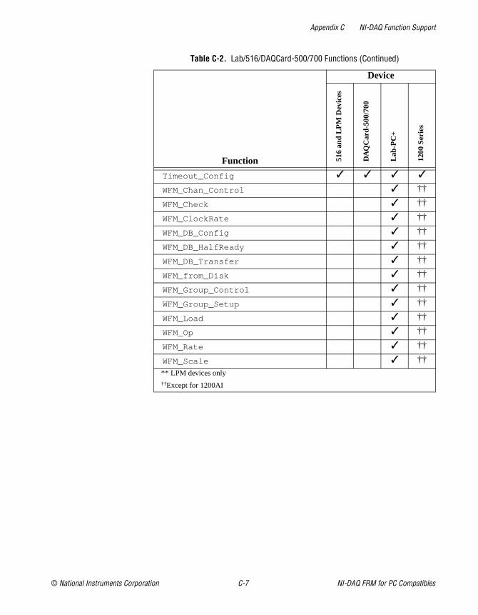
Appendix C NI-DAQ Function Support
© National Instruments Corporation C-7 NI-DAQ FRM for PC Compatibles
Timeout_Config
WFM_Chan_Control ††
WFM_Check ††
WFM_ClockRate ††
WFM_DB_Config ††
WFM_DB_HalfReady ††
WFM_DB_Transfer ††
WFM_from_Disk ††
WFM_Group_Control ††
WFM_Group_Setup ††
WFM_Load ††
WFM_Op ††
WFM_Rate ††
WFM_Scale ††** LPM devices only ††Except for 1200AI
Table C-2. Lab/516/DAQCard-500/700 Functions (Continued)
Function
Device
516
and
LPM
Dev
ices
DA
QC
ard-
500/
700
Lab-
PC
+
1200
Ser
ies

Appendix C NI-DAQ Function Support
NI-DAQ FRM for PC Compatibles C-8 www.natinst.com
Table C-3. DSA Device Functions
Function
Device
PC
I-44
51
PC
I-44
53
NI 4
551
PC
I-44
52
PC
I-44
54
NI 4
552
AI_Change_Parameter
AO_Change_Parameter
AO_Configure
Config_HW_Analog_Trigger
DAQ_Check
DAQ_Clear
DAQ_Config
DAQ_DB_Config
DAQ_DB_HalfReady
DAQ_DB_Transfer
DAQ_Monitor
DAQ_Op
DAQ_Set_Clock
DAQ_Start
DAQ_StopTrigger_Config
DAQ_to_Disk
DAQ_VScale
DIG_In_Line
DIG_In_Prt
DIG_Line_Config
DIG_Out_Line
DIG_Out_Prt
DIG_Prt_Config
Get_DAQ_Device_Info
GPCTR_Change_Parameter
GPCTR_Config_Buffer
GPCTR_Control
GPCTR_Read_Buffer
GPCTR_Set_Application

Appendix C NI-DAQ Function Support
© National Instruments Corporation C-9 NI-DAQ FRM for PC Compatibles
GPCTR_Watch
Init_DA_Brds
SCAN_Op
SCAN_Setup
SCAN_Start
SCAN_to_Disk
Select_Signal
Set_DAQ_Device_Info
Timeout_Config
WFM_Check
WFM_DB_Config
WFM_DB_HalfReady
WFM_DB_Transfer
WFM_from_Disk
WFM_Group_Control
WFM_Group_Setup
WFM_Load
WFM_Op
WFM_Scale
WFM_Set_Clock
Table C-3. DSA Device Functions (Continued)
Function
Device
PC
I-44
51
PC
I-44
53
NI 4
551
PC
I-44
52
PC
I-44
54
NI 4
552

Appendix C NI-DAQ Function Support
NI-DAQ FRM for PC Compatibles C-10 www.natinst.com
Table C-4. Analog Output Family Functions
Function
Device
AO
-2D
C S
erie
s
AT-A
O-6
/10
VX
I-A
O-4
8XD
C
6703
/670
4 S
erie
s
671x
AO_Calibrate
AO_Change_Parameter
AO_Configure
AO_Update
AO_VScale
AO_VWrite
AO_Write
Calibrate_E_Series
Config_DAQ_Event_Message
DIG_In_Line
DIG_In_Prt
DIG_Line_Config
DIG_Out_Line
DIG_Out_Prt
DIG_Prt_Config
Get_DAQ_Device_Info
Get_NI_DAQ_Version
GPCTR_Change_Parameter
GPCTR_Config_Buffer
GPCTR_Control
GPCTR_Set_Application
GPCTR_Watch
Init_DA_Brds
RTSI_Clear
RTSI_Clock
RTSI_Conn
RTSI_DisConn
Select_Signal

Appendix C NI-DAQ Function Support
© National Instruments Corporation C-11 NI-DAQ FRM for PC Compatibles
Set_DAQ_Device_Info
Timeout_Config
WFM_Chan_Control
WFM_Check
WFM_ClockRate
WFM_DB_Config
WFM_DB_HalfReady
WFM_DB_Transfer
WFM_from_Disk
WFM_Group_Control
WFM_Group_Setup
WFM_Load
WFM_Op
WFM_Rate
WFM_Scale
Table C-4. Analog Output Family Functions (Continued)
Function
Device
AO
-2D
C S
erie
s
AT-A
O-6
/10
VX
I-A
O-4
8XD
C
6703
/670
4 S
erie
s
671x

Appendix C NI-DAQ Function Support
NI-DAQ FRM for PC Compatibles C-12 www.natinst.com
Table C-5. Digital I/O Family Functions
Function
Device
AT-D
IO-3
2F
DA
QD
IO 6
533
(DIO
-32H
S)
DIO
-24
(650
3) a
nd D
IO-9
6
PC
-OP
DIO
-16
VX
I-D
IO-1
28
652X
Align_DMA_Buffer
Config_DAQ_Event_Message
DIG_Block_Check
DIG_Block_Clear
DIG_Block_In
DIG_Block_Out
DIG_Block_PG_Config
DIG_Change_Message_Config
DIG_Change_Message_Control
DIG_DB_Config
DIG_DB_HalfReady
DIG_DB_Tansfer
DIG_Filter_Config
DIG_GRP_Config
DIG_GRP_Mode
DIG_GRP_Status
DIG_In_Grp
DIG_In_Line
DIG_In_Prt
DIG_Line_Config
DIG_Out_Grp
DIG_Out_Line
DIG_Out_Prt
DIG_Prt_Config
DIG_Prt_Status

Appendix C NI-DAQ Function Support
© National Instruments Corporation C-13 NI-DAQ FRM for PC Compatibles
DIG_SCAN_Setup
DIG_Trigger_Config
Get_DAQ_Device_Info
Get_NI_DAQ_Version
Init_DA_Brds
RTSI_Clear
RTSI_Clock
RTSI_Conn
RTSI_DisConn
Set_DAQ_Device_Info
Timeout_Config
Table C-6. Timing Device Functions
Function
Device
PC
-TIO
-10
660X
(ex
cept
660
8)
6608
Calibrate_TIO
Config_DAQ_Event_Message
CTR_Config
CTR_EvCount
CTR_EvRead
CTR_FOUT_Config
Table C-5. Digital I/O Family Functions (Continued)
Function
Device
AT-D
IO-3
2F
DA
QD
IO 6
533
(DIO
-32H
S)
DIO
-24
(650
3) a
nd D
IO-9
6
PC
-OP
DIO
-16
VX
I-D
IO-1
28
652X
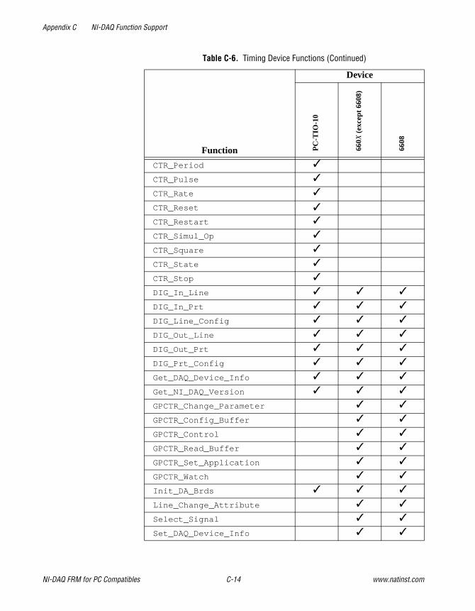
Appendix C NI-DAQ Function Support
NI-DAQ FRM for PC Compatibles C-14 www.natinst.com
CTR_Period
CTR_Pulse
CTR_Rate
CTR_Reset
CTR_Restart
CTR_Simul_Op
CTR_Square
CTR_State
CTR_Stop
DIG_In_Line
DIG_In_Prt
DIG_Line_Config
DIG_Out_Line
DIG_Out_Prt
DIG_Prt_Config
Get_DAQ_Device_Info
Get_NI_DAQ_Version
GPCTR_Change_Parameter
GPCTR_Config_Buffer
GPCTR_Control
GPCTR_Read_Buffer
GPCTR_Set_Application
GPCTR_Watch
Init_DA_Brds
Line_Change_Attribute
Select_Signal
Set_DAQ_Device_Info
Table C-6. Timing Device Functions (Continued)
Function
Device
PC
-TIO
-10
660X
(ex
cept
660
8)
6608

Appendix C NI-DAQ Function Support
© National Instruments Corporation C-15 NI-DAQ FRM for PC Compatibles
Table C-7. SCXI Functions
Function
Module Device
SC
XI-
1100
SC
XI-
1101
1102
Ser
ies
SC
XI-
1104
SC
XI-
1112
SC
XI-
1120
, SC
XI-
1120
D
SC
XI-
1121
SC
XI-
1122
SC
XI-
1124
SC
XI-
1125
SC
XI-
1126
SC
XI-
1127
SC
XI-
1140
SC
XI-
1141
, SC
XI-
1142
, SC
XI-
1143
SC
XI-
1160
SC
XI-
1161
SC
XI-
1162
/116
2HV
SC
XI-
1163
/116
3R
VX
I-S
C-1
150
SC
XI-
1200
DA
QC
ard-
700
DIO
Dev
ices
Lab
and
1200
Dev
ices
(exc
ept D
AQ
Pad
-120
0 an
d S
CX
I-12
00)
MIO
and
AI D
evic
es
LPM
Dev
ices
SCXI_AO_Write
SCXI_Cal_Constants
SCXI_Calibrate
SCXI_Calibrate_Setup
SCXI_Change_Chan
SCXI_Configure_Filter
SCXI_Get_Chassis_Info
SCXI_Get_Module_Info
SCXI_Get_State
SCXI_Get_Status
SCXI_Load_Config
SCXI_ModuleID_Read
SCXI_MuxCtr_Setup
SCXI_Reset
SCXI_Scale
SCXI_SCAN_Setup
SCXI_Set_Config
SCXI_Set_Gain
SCXI_Set_Input_Mode
SCXI_Set_State
SCXI_Single_Chan_Setup
SCXI_Track_Hold_Control
SCXI_Track_Hold_Setup

© National Instruments Corporation D-1 NI-DAQ FRM for PC Compatibles
DTechnical Support Resources
This appendix describes the comprehensive resources available to you in the Technical Support section of the National Instruments Web site and provides technical support telephone numbers for you to use if you have trouble connecting to our Web site or if you do not have internet access.
NI Web SupportTo provide you with immediate answers and solutions 24 hours a day, 365 days a year, National Instruments maintains extensive online technical support resources. They are available to you at no cost, are updated daily, and can be found in the Technical Support section of our Web site at www.natinst.com/support .
Online Problem-Solving and Diagnostic Resources• KnowledgeBase—A searchable database containing thousands of
frequently asked questions (FAQs) and their corresponding answers or solutions, including special sections devoted to our newest products. The database is updated daily in response to new customer experiences and feedback.
• Troubleshooting Wizards—Step-by-step guides lead you through common problems and answer questions about our entire product line. Wizards include screen shots that illustrate the steps being described and provide detailed information ranging from simple getting started instructions to advanced topics.
• Product Manuals—A comprehensive, searchable library of the latest editions of National Instruments hardware and software product manuals.
• Hardware Reference Database—A searchable database containing brief hardware descriptions, mechanical drawings, and helpful images of jumper settings and connector pinouts.
• Application Notes—A library with more than 100 short papers addressing specific topics such as creating and calling DLLs, developing your own instrument driver software, and porting applications between platforms and operating systems.

Appendix D Technical Support Resources
NI-DAQ FRM for PC Compatibles D-2 www.natinst.com
Software-Related Resources• Instrument Driver Network —A library with hundreds of instrument
drivers for control of standalone instruments via GPIB, VXI, or serial interfaces. You also can submit a request for a particular instrument driver if it does not already appear in the library.
• Example Programs Database—A database with numerous, non-shipping example programs for National Instruments programming environments. You can use them to complement the example programs that are already included with National Instruments products.
• Software Library —A library with updates and patches to application software, links to the latest versions of driver software for National Instruments hardware products, and utility routines.
Worldwide SupportNational Instruments has offices located around the globe. Many branch offices maintain a Web site to provide information on local services. You can access these Web sites from www.natinst.com/worldwide .
If you have trouble connecting to our Web site, please contact your local National Instruments office or the source from which you purchased your National Instruments product(s) to obtain support.
For telephone support in the United States, dial 512 795 8248. For telephone support outside the United States, contact your local branch office:
Australia 03 9879 5166, Austria 0662 45 79 90 0, Belgium 02 757 00 20, Brazil 011 284 5011, Canada (Calgary) 403 274 9391, Canada (Ontario) 905 785 0085, Canada (Québec) 514 694 8521, China 0755 3904939, Denmark 45 76 26 00, Finland 09 725 725 11, France 01 48 14 24 24, Germany 089 741 31 30, Greece 30 1 42 96 427 Hong Kong 2645 3186, India 91805275406, Israel 03 6120092, Italy 02 413091, Japan 03 5472 2970, Korea 02 596 7456, Mexico (D.F.) 5 280 7625, Mexico (Monterrey) 8 357 7695, Netherlands 0348 433466, Norway 32 27 73 00, Singapore 2265886, Spain (Barcelona) 93 582 0251, Spain (Madrid) 91 640 0085, Sweden 08 587 895 00, Switzerland 056 200 51 51, Taiwan 02 2377 1200, United Kingdom 01635 523545

© National Instruments Corporation G-1 NI-DAQ FRM for PC Compatibles
Glossary
Prefix Meaning Value
p- pico- 10–12
n- nano- 10–9
µ- micro- 10– 6
m- milli- 10–3
k- kilo- 103
M- mega- 106
G- giga- 109
t- tera- 1012
Numbers/Symbols
° degree
< less than or equal to
– minus
% percent
+ plus
± plus or minus
Ω ohm
A
AC alternating current
ACK acknowledge
A/D analog-to-digital

Glossary
NI-DAQ FRM for PC Compatibles G-2 www.natinst.com
ADC A/D converter
ADC resolution the resolution of the ADC, which is measured in bits. An ADC with 16 bits has a higher resolution, and thus a higher degree of accuracy, than a 12-bit ADC.
ADE Application Development Environment. See IDE.
address character code that identifies a specific location (or series of locations) in memory
AI Analog Input
AISENSE analog input sense signal
alias a false lower frequency component that appears in sampled data acquired at too low a sampling rate
AMUX AMUX-64T
API application programming interface
asynchronous (1) hardware—a property of an event that occurs at an arbitrary time, without synchronization to a reference clock (2) software—a property of a function that begins an operation and returns prior to the completion or termination of the operation
attenuate to decrease the amplitude of a signal
B
b bit—one binary digit, either 0 or 1
B byte—eight related bits of data, an eight-bit binary number. Also used to denote the amount of memory required to store one byte of data.
base address a memory address that serves as the starting address for programmable registers. All other addresses are located by adding to the base address.
BCD binary-coded decimal
binary a number system with a base of 2

Glossary
© National Instruments Corporation G-3 NI-DAQ FRM for PC Compatibles
bipolar a signal range that includes both positive and negative values (for example, –5 V to +5 V)
buffer temporary storage for acquired or generated data (software)
burst-mode a high-speed data transfer in which the address of the data is sent followed by back-to-back data words while a physical signal is asserted
bus the group of conductors that interconnect individual circuitry in a computer. Typically, a bus is the expansion vehicle to which I/O or other devices are connected. Examples of PC buses are the ISA and PCI bus.
C
C Celsius
CalDAC calibration DAC
calibration constants
cascading process of extending the counting range of a counter chip by connecting to the next higher counter
channel pin or wire lead to which you apply or from which you read the analog or digital signal. Analog signals can be single-ended or differential. For digital signals, you group channels to form ports. Ports usually consist of either four or eight digital channels.
channel clock the clock controlling the time interval between individual channel sampling within a scan. Boards with simultaneous sampling do not have this clock.
CI computing index
clock hardware component that controls timing for reading from or writing to groups
counter/timer a circuit that counts external pulses or clock pulses (timing)
CPU central processing unit

Glossary
NI-DAQ FRM for PC Compatibles G-4 www.natinst.com
D
D/A digital-to-analog
DAC D/A converter
DAQ data acquisition—(1) collecting and measuring electrical signals from sensors, transducers, and test probes or fixtures and inputting them to a computer for processing; (2) collecting and measuring the same kinds of electrical signals with A/D and/or DIO boards plugged into a computer, and possibly generating control signals with D/A and/or DIO boards in the same computer
dB decibel—the unit for expressing a logarithmic measure of the ratio of two signal levels: dB=20log10 V1/V2, for signals in volts
DC direct current
default setting a default parameter value recorded in the driver. In many cases, the default input of a control is a certain value (often 0) that means use the current default setting. For example, the default input for a parameter may be do not change current setting, and the default setting may be no AMUX-64T boards. If you do change the value of such a parameter, the new value becomes the new setting. You can set default settings for some parameters in the configuration utility or manually using switches located on the device.
device a plug-in data acquisition board, card, or pad that can contain multiple channels and conversion devices. Plug-in boards, PCMCIA cards, and devices such as the DAQPad-1200, which connects to your computer parallel port, are all examples of DAQ devices. SCXI modules are distinct from devices, with the exception of the SCXI-1200, which is a hybrid.
DIG digital
digital port See port.
DIN Deutsche Industrie Norme
DIO digital I/O
DIP dual inline package
dithering the addition of Gaussian noise to an analog input signal

Glossary
© National Instruments Corporation G-5 NI-DAQ FRM for PC Compatibles
DLL dynamic-dynamic link library
DMA direct memory access
DNL differential nonlinearity—a measure in LSB of the worst-case deviation of code widths from their ideal value of 1 LSB
drivers software that controls a specific hardware device such as a DAQ board or a GPIB interface board
DSP digital signal processing
E
EEPROM electronically erasable programmable read-only memory
EISA Extended Industry Standard Architecture
ETS Equivalent Time Sampling
F
fetch-and-deposit a data transfer in which the data bytes are transferred from the source to the controller, and then from the controller to the target
FIFO first-in first-out memory buffer—the first data stored is the first data sent to the acceptor. FIFOs are often used on DAQ devices to temporarily store incoming or outgoing data until that data can be retrieved or output. For example, an analog input FIFO stores the results of A/D conversions until the data can be retrieved into system memory, a process that requires the servicing of interrupts and often the programming of the DMA controller. This process can take several milliseconds in some cases. During this time, data accumulates in the FIFO for future retrieval. With a larger FIFO, longer latencies can be tolerated. In the case of analog output, a FIFO permits faster update rates, because the waveform data can be stored on the FIFO ahead of time. This again reduces the effect of latencies associated with getting the data from system memory to the DAQ device.
filtering a type of signal conditioning that allows you to filter unwanted signals from the signal you are trying to measure
ft feet

Glossary
NI-DAQ FRM for PC Compatibles G-6 www.natinst.com
G
gain The factor by which a signal is amplified; sometimes expressed in decibels
H
h hour
handle pointer to a pointer to a block of memory; handles reference arrays and strings. An array of strings is a handle to a block of memory containing handles to strings.
handshaked digital I/O a type of digital acquisition/generation where a device or module accepts or transfers data after a digital pulse has been received. Also called latched digital I/O.
hardware the physical components of a computer system, such as the circuit boards, plug-in boards, chassis, enclosures, peripherals, and cables
hardware triggering a form of triggering where you set the start time of an acquisition and gather data at a known position in time relative to a trigger signal
hex hexadecimal
Hz hertz
I
ID identification
IDE integrated development environment
IEEE Institute of Electrical and Electronics Engineers
instrument driver a set of high-level software functions that controls a specific GPIB, VXI, or RS-232 programmable instrument or a specific plug-in DAQ board. Instrument drivers are available in several forms, ranging from a function callable language to a virtual instrument (VI) in LabVIEW.
interrupt a computer signal indicating that the CPU should suspend its current task to service a designated activity
interrupt level the relative priority at which a device can interrupt

Glossary
© National Instruments Corporation G-7 NI-DAQ FRM for PC Compatibles
I/O input/output—the transfer of data to/from a computer system involving communications channels, operator interface devices, and/or data acquisition and control interfaces
IRQ interrupt request
ISA Industry Standard Architecture
K
k kilo—the standard metric prefix for 1,000, or 103, used with units of measure such as volts, hertz, and meters
K kilo—the prefix for 1,024, or 210, used with B in quantifying data or computer memory
kbytes/s a unit for data transfer that means 1,000 or 103 bytes/s
Kword 1,024 words of memory
L
LabVIEW laboratory virtual instrument engineering workbench
latched digital I/O a type of digital acquisition/generation where a device or module accepts or transfers data after a digital pulse has been received. Also called handshaked digital I/O.
LED light-emitting diode
library a file containing compiled object modules, each comprised of one of more functions, that can be linked to other object modules that make use of these functions. NIDAQMSC.LIB is a library that contains NI-DAQ functions. The NI-DAQ function set is broken down into object modules so that only the object modules that are relevant to your application are linked in, while those object modules that are not relevant are not linked.
LSB least significant bit

Glossary
NI-DAQ FRM for PC Compatibles G-8 www.natinst.com
M
m meters
M (1) Mega, the standard metric prefix for 1 million or 106, when used with units of measure such as volts and hertz; (2) mega, the prefix for 1,048,576, or 220, when used with B to quantify data or computer memory
MB megabytes of memory
MBLT eight-byte block transfers in which both the Address bus and the Data bus are used to transfer data
Mbytes/s a unit for data transfer that means 1 million or 106 bytes/s
MC Micro Channel
memory buffer See buffer.
min minutes
MIO multifunction I/O
MITE MXI Interfaces to Everything—a custom ASIC designed by National Instruments that implements the PCI bus interface. The MITE supports bus mastering for high speed data transfers over the PCI bus.
MS million samples
MSB most significant bit
multiplexed mode an SCXI operating mode in which analog input channels are multiplexed into one module output so that your cabled DAQ device has access to the module’s multiplexed output as well as the outputs on all other multiplexed modules in the chassis through the SCXI bus. Also called serial mode.
mux multiplexer—a switching device with multiple inputs that sequentially connects each of its inputs to its output, typically at high speeds, in order to measure several signals with a single analog input channel

Glossary
© National Instruments Corporation G-9 NI-DAQ FRM for PC Compatibles
N
NC Normally Closed
NI-DAQ National Instruments driver software for DAQ hardware
NIST National Institute of Standards and Technology
NI-TIO National Instruments Timing Input/Output controller. An ASIC National Instruments designed for high-speed counter/timer applications.
NO Normally Open
nonlatched digital I/O a type of digital acquisition/generation where LabVIEW updates the digital lines or port states immediately or returns the digital value of an input line. Also called immediate digital I/O or non-handshaking.
nonreferenced signal sources
signal sources with voltage signals that are not connected to an absolute reference or system ground. Also called floating signal sources. Some common example of nonreferenced signal sources are batteries, transformers, or thermocouples.
NRSE nonreferenced single-ended mode—all measurements are made with respect to a common (NRSE) measurement system reference, but the voltage at this reference can vary with respect to the measurement system ground
O
onboard channels channels provided by the plug-in data acquisition board
onboard RAM optional RAM usually installed into SIMM slots
operating system base-level software that controls a computer, runs programs, interacts with users, and communicates with installed hardware or peripheral devices
optical coupler, optocoupler
a device designed to transfer electrical signals by utilizing light waves to provide coupling with electrical isolation between input and output. Sometimes called optoisolator or photocoupler.
OUT Output

Glossary
NI-DAQ FRM for PC Compatibles G-10 www.natinst.com
P
parallel mode a type of SCXI operating mode in which the module sends each of its input channels directly to a separate analog input channel of the device to the module
pattern generation a type of handshaked (latched) digital I/O in which internal counters generate the handshaked signal, which in turn initiates a digital transfer. Because counters output digital pulses at a constant rate, this means you can generate and retrieve patterns at a constant rate because the handshaked signal is produced at a constant rate.
PC personal computer
PC Card a credit-card-sized expansion card that fits in a PCMCIA slot often referred to as a PCMCIA card
PCI peripheral component interconnect
PCMCIA an expansion bus architecture that has found widespread acceptance as a de facto standard in notebook-size computers. It originated as a specification for add-on memory cards written by the Personal Computer Memory Card International Association.
PFI programmable function input
Plug and Play devices devices that do not require dip switches or jumpers to configure resources on the devices—also called switchless devices
Plug and Play ISA a specification prepared by Microsoft, Intel, and other PC-related companies that result in PCs with plug-in boards that can be fully configured in software, without jumpers or switches on the boards
port (1) a communications connection on a computer or a remote controller (2) a digital port, consisting of four or eight lines of digital input and/or output
posttriggering the technique used on a DAQ board to acquire a programmed number of samples after trigger conditions are met
pts points
PXI PCI eXtensions for Instrumentation. PXI is an open specification that builds off the CompactPCI specification by adding instrumentation-specific features.
Glossary
© National Instruments Corporation G-11 NI-DAQ FRM for PC Compatibles
R
RAM random-access memory
real time a property of an event or system in which data is processed as it is acquired instead of being accumulated and processed at a later time
REQ request
rms root mean square
ROM read-only memory
RSE referenced single-ended mode—all measurements are made with respect to a common reference measurement system or a ground. Also called a grounded measurement system.
RTSI bus real-time system integration bus—the National Instruments timing bus that connects DAQ boards directly, by means of connectors on top of the boards, for precise synchronization of functions
S
s seconds
S samples
sample counter the clock that counts the output of the channel clock, in other words, the number of samples taken. On boards with simultaneous sampling, this counter counts the output of the scan clock and hence the number of scans.
scan one or more analog or digital input samples. Typically, the number of input samples in a scan is equal to the number of channels in the input group. For example, one pulse from the scan clock produces one scan which acquires one new sample from every analog input channel in the group.
scan clock the clock controlling the time interval between scans. On boards with interval scanning support (for example, the AT-MIO-16F-2), this clock gates the channel clock on and off. On boards with simultaneous sampling (for example, the PCI-6110E), this clock clocks the ACDs.
scan rate the number of scans per second. For example, a scan rate of 10 Hz means sampling each channel 10 times per second.

Glossary
NI-DAQ FRM for PC Compatibles G-12 www.natinst.com
SCXI Signal Conditioning eXtensions for Instrumentation
SDK Software Development Kit
SE single-ended—a term used to describe an analog input that is measured with respect to a common ground
self-calibrating a property of a DAQ board that has an extremely stable onboard reference and calibrates its own A/D and D/A circuits without manual adjustments by the user
shared memory See dual-access memory
signal conditioning the manipulation of signals to prepare them for digitizing
software trigger a programmed event that triggers an event such as data acquisition
software triggering a method of triggering in which you simulate an analog trigger using software. Also called conditional retrieval.
SS simultaneous sampling—a property of a system in which each input or output channel is digitized or updated at the same instant
S/s samples per second
STB Strobe Input Signal
STC system timing controller
switchless device devices that do not require dip switches or jumpers to configure resources on the devices—also called Plug and Play devices
synchronous (1) hardware—a property of an event that is synchronized to a reference clock (2) software—a property of a function that begins an operation and returns only when the operation is complete
T
TC terminal count
T/H track-and-hold—a circuit that tracks an analog voltage and holds the value on command

Glossary
© National Instruments Corporation G-13 NI-DAQ FRM for PC Compatibles
transfer rate the rate, measured in bytes/s, at which data is moved from source to destination after software initialization and set up operations; the maximum rate at which the hardware can operate
trigger any event that causes or starts some form of data capture
TTL transistor-transistor logic
U
UI update interval
unipolar a signal range that is always positive (for example, 0 to +10 V)
update the output equivalent of a scan. One or more analog or digital output samples. Typically, the number of output samples in an update is equal to the number of channels in the output group. For example, one pulse from the update clock produces one update which sends one new sample to every analog output channel in the group.
update rate the number of output updates per second
USB Universal Serial Bus
V
V volts
W
waveform multiple voltage readings taken at a specific sampling rate
WF waveform
wire data path between nodes
word the standard number of bits that a processor or memory manipulates at one time. Microprocessors typically use 8-bit, 16-bit, or 32-bit words.
X
XMS extended memory specification

© National Instruments Corporation I-1 NI-DAQ FRM for PC Compatibles
Index
Numbers660X device parameters, Select_Signal function,
2-414 to 2-4198253 counter (ICTR) functions. See
counter/timer functions.
AAI and MIO device function support (table),
C-1 to C-4AI_Change_Parameter function, 2-1 to 2-2AI_Check function, 2-3 to 2-4AI_Clear function, 2-5AI_Configure function, 2-6 to 2-9AI_Get_Overloaded_Channels function,
2-10 to 2-11AI_MUX_Config function, 2-12 to 2-13AI_Read function, 2-14 to 2-15AI_Read_Scan function, 2-16AI_Setup function, 2-17AI_VRead function, 2-18 to 2-19AI_VRead_Scan function, 2-20AI_VScale function, 2-21 to 2-22Align_DMA_Buffer function, 2-23 to 2-25Am9513 counter (CTR) functions. See
counter/timer functions.AMUX-64T boards, configuring, 2-12 to 2-13analog input calibration, SCXI modules,
2-345 to 2-347analog input channel settings
DAQ devices (table), B-1 to B-2internal channel purposes for analog input
devices (table), B-6valid internal analog input channels (table),
B-2 to B-6
analog input functionsAI_Change_Parameter, 2-1 to 2-2AI_Check, 2-3 to 2-4AI_Clear, 2-5AI_Configure, 2-6 to 2-9AI_Get_Overloaded_Channels,
2-10 to 2-11AI_MUX_Config, 2-12 to 2-13AI_Read, 2-14 to 2-15AI_Setup, 2-17AI_VRead, 2-18 to 2-19AI_VScale, 2-21 to 2-22Configure_HW_Analog_Trigger,
2-84 to 2-90DAQ_Check function, 2-116 to 2-117DAQ_Clear, 2-118DAQ_Config, 2-119 to 2-121DAQ_DB_Config, 2-122DAQ_DB_HalfReady, 2-123 to 2-124DAQ_DB_Transfer, 2-125 to 2-126DAQ_Monitor, 2-127 to 2-129DAQ_Rate, 2-133 to 2-134DAQ_Set_Clock, 2-135 to 2-136DAQ_Start, 2-137 to 2-140DAQ_StopTrigger_Config, 2-141 to 2-142DAQ_VScale, 2-146 to 2-147definition, 1-12Lab_ISCAN_Check, 2-282 to 2-283Lab_ISCAN_Start, 2-289 to 2-292LabWindows/CVI function panel tree,
1-6 to 1-8NI-DAQ function support (table)
DSA devices, C-8 to C-9Lab/516/DAQCard-500/700 devices,
C-5 to C-7MIO and AI devices, C-1 to C-3
SCAN_Demux, 2-313 to 2-314

Index
NI-DAQ FRM for PC Compatibles I-2 www.natinst.com
SCAN_Sequence_Demux, 2-318 to 2-320
SCAN_Sequence_Retrieve, 2-321SCAN_Sequence_Setup, 2-322 to 2-324SCAN_Setup, 2-325 to 2-327SCAN_Start, 2-328 to 2-333Select_Signal, 2-401 to 2-423
analog output calibration, SCXI modules, 2-347 to 2-348
analog output functions. See also waveform generation functions.
AO_Change_Parameter, 2-28 to 2-34AO_Configure, 2-35 to 2-38AO_Update, 2-39AO_VScale, 2-40 to 2-41AO_VWrite, 2-42 to 2-43AO_Write, 2-44 to 2-45definition, 1-13LabWindows/CVI function panel tree,
1-8 to 1-9NI-DAQ function support (table)
analog output family of devices, C-10 to C-11
Lab/516/DAQCard-500/700 functions, C-5 to C-7
MIO and AI devices, C-2, C-4analog trigger event (figure), 2-71AO_Calibrate function, 2-26 to 2-27AO_Change_Parameter function, 2-28 to 2-34
description, 2-28 to 2-29end of buffer interrupts, 2-33FIFO transfer condition, 2-30FIFO transfer count, 2-31 to 2-32ground DAC reference, 2-32memory transfer width, 2-34output attenuation, 2-32 to 2-33output enable, 2-32reglitching, 2-29voltage or current output, 2-29 to 2-30
AO_Configure function, 2-35 to 2-38AO_Update function, 2-39
AO_VScale function, 2-40 to 2-41AO_VWrite function, 2-42 to 2-43AO_Write function, 2-44 to 2-45arrays, 1-3
Bblock transfer functions. See digital I/O
functions.Borland Delphi, 1-4buffer interrupts, enabling/disabling, 2-38buffered counting and time measurement
event counting application, 2-253 to 2-255
period measurement application, 2-255 to 2-257
pulse width measurement application, 2-259 to 2-260
semi-period measurement application, 2-257 to 2-258
time interval between aux line nad gate signal transitions, 2-260 to 2-262
CCalibrate_1200 function, 2-45 to 2-51Calibrate_DSA function, 2-52 to 2-54
description, 2-52 to 2-53external calibration, 2-53restoring factory calibration, 2-54self-calibration, 2-53
Calibrate_E_Series function, 2-55 to 2-60calibration constant loading by
NI-DAQ, 2-60calibration constants, 2-56changing default load area, 2-57description, 2-55 to 2-57external calibration, 2-58 to 2-59self-calibration, 2-58

Index
© National Instruments Corporation I-3 NI-DAQ FRM for PC Compatibles
Calibrate_TIO function, 2-61 to 2-63calibration constants, 2-62changing default load area, 2-63description, 2-61 to 2-63external calibration, 2-63restoring factory calibration, 2-63
calibration functionsAO_Calibrate, 2-26 to 2-27Calibrate_1200, 2-45 to 2-51Calibrate_DSA, 2-52 to 2-54Calibrate_E_Series function, 2-55 to 2-60Calibrate_TIO, 2-61 to 2-63definition, 1-12LabWindows/CVI function panel
tree, 1-6LPM16_Calibrate, 2-299SCXI_Cal_Constants, 2-341 to 2-348SCXI_Calibrate, 2-349 to 2-351SCXI_Calibrate_Setup, 2-354 to 2-355
change notification functions. See digital I/O functions.
channel settings. See analog input channel settings.
Config_Alarm_Deadband functiondescription, 2-64 to 2-67high alarm deadband (figure), 2-66low alarm deadband (figure), 2-67
Config_ATrig_Event_Message function, 2-68 to 2-71
Config_DAQ_Event_Message function, 2-73 to 2-83
callback functions, 2-83DAQ event messages (table), 2-75 to 2-78description, 2-73 to 2-81example, 2-82 to 2-83usable parameters for DAQ event codes
(table), 2-80using the function, 2-81 to 2-83valid counters and external timing signals
for DAQEvent=9 (table), 2-79
configuration functionsAI_Configure, 2-6 to 2-9AI_MUX_Config, 2-12 to 2-13AO_Configure, 2-35 to 2-38Config_Alarm_Deadband, 2-64 to 2-67Config_ATrig_Event_Message,
2-68 to 2-71Configure_HW_Analog_Trigger,
2-84 to 2-90CTR_Config, 2-91 to 2-92CTR_FOUT_Config, 2-97 to 2-98DAQ_Config, 2-119 to 2-121DAQ_DB_Config, 2-122DAQ_StopTrigger_Config,
2-141 to 2-142definition, 1-12DIG_Block_PG_Config, 2-155 to 2-158DIG_Change_Message_Config,
2-159 to 2-161DIG_DB_Config, 2-163 to 2-164DIG_Filter_Config, 2-169 to 2-170DIG_Grp_Config, 2-171 to 2-172DIG_Line_Config, 2-184 to 2-185DIG_Prt_Config, 2-191 to 2-193DIG_SCAN_Setup, 2-196 to 2-199DIG_Trigger_Config, 2-200 to 2-202GPCTR_Config_Buffer, 2-222 to 2-223ICTR_Setup, 2-270 to 2-273LabWindows/CVI function panel
tree, 1-6MIO_Config, 2-300 to 2-301SC_2040_Config function,
2-311 to 2-312SCXI_Configure_Filter, 2-357 to 2-359SCXI_Get_Chassis_Info, 2-360 to 2-361SCXI_Get_Module_Info, 2-362 to 2-363SCXI_Load_Config, 2-368SCXI_MuxCtr_Setup, 2-371 to 2-372SCXI_SCAN_Setup, 2-380 to 2-382SCXI_Set_Config, 2-383 to 2-386

Index
NI-DAQ FRM for PC Compatibles I-4 www.natinst.com
SCXI_Single_Chan_Setup, 2-394SCXI_Track_Hold_Setup, 2-397 to 2-400Timeout_Config, 2-434 to 2-435WFM_DB_Config, 2-445 to 2-446WFM_Group_Setup, 2-456 to 2-457
Configure_HW_Analog_Trigger function, 2-84 to 2-90
description, 2-84 to 2-88ND_ABOVE_HIGH_LEVEL
(figure), 2-86ND_BELOW_LOW_LEVEL
(figure), 2-86ND_HIGH_HYSTERESIS (figure), 2-87ND_INSIDE_REGION (figure), 2-87ND_LOW_HYSTERESIS (figure), 2-87using the function, 2-88 to 2-90
counter/timer functions8253 counters (ICTR)
ICTR_Read, 2-267 to 2-268ICTR_Reset, 2-269ICTR_Setup, 2-270 to 2-273LabWindows/CVI function panel
tree, 1-12Am9513 counters (CTR)
CTR_Config function, 2-91 to 2-92CTR_EvCount function, 2-93 to 2-94CTR_EvRead function, 2-95 to 2-96CTR_FOUT_Config, 2-97 to 2-98CTR_Period function, 2-99 to 2-100CTR_Pulse function, 2-101 to 2-104CTR_Rate, 2-105 to 2-106CTR_Reset, 2-107CTR_Restart, 2-108CTR_Simul_Op, 2-109 to 2-110CTR_Square, 2-111 to 2-113CTR_State, 2-114CTR_Stop function, 2-115LabWindows/CVI function panel
tree, 1-11 to 1-12
DAQ-STC and NI-TIO counters (GPCTR)
GPCTR_Change_Parameter,2-207 to 2-221
GPCTR_Config_Buffer, 2-222 to 2-223
GPCTR_Control, 2-224 to 2-226GPCTR_Read_Buffer,
2-227 to 2-229GPCTR_Set_Application,
2-230 to 2-263GPCTR_Watch, 2-264 to 2-266LabWindows/CVI function panel
tree, 1-11definition, 1-13LabWindows/CVI function panel tree,
1-11 to 1-12NI-DAQ function support (table)
DSA devices, C-8 to C-9Lab/516/DAQCard-500/700 devices,
C-5 to C-7MIO and AI devices, C-3timing devices, C-13 to C-14
counting and time measurement applications. See also buffered counting and time measurement.
event counting application, 2-232 to 2-233
single period measurement,2-234 to 2-236
single pulse width measurement, 2-236 to 2-238
time interval between aux line and gate signal transitions, 2-241 to 2-243
triggered pulse width measurement, 2-238 to 2-241
DDAQ_Check function, 2-116 to 2-117DAQ_Clear function, 2-118DAQ_Config function, 2-119 to 2-121

Index
© National Instruments Corporation I-5 NI-DAQ FRM for PC Compatibles
DAQ_DB_Config function, 2-122DAQ_DB_HalfReady function,
2-123 to 2-124DAQ_DB_Transfer function, 2-125 to 2-126DAQ_Monitor function, 2-127 to 2-129
DAQ_Op function, 2-130 to 2-132DAQ_Rate function, 2-133 to 2-134DAQ_Set_Clock function, 2-135 to 2-136DAQ_Start function, 2-137 to 2-140DAQ-STC counter functions. See
counter/timer functions.DAQ_StopTrigger_Config function,
2-141 to 2-142DAQ_to_Disk function, 2-143 to 2-145DAQ_VScale function, 2-146 to 2-147data acquisition. See LabWindows/CVI
function tree for data acquisition.data types. See variable data types.demultiplexing functions
SCAN_Demux, 2-313 to 2-314SCAN_Sequence_Demux,
2-318 to 2-320devices
device numbers, 1-2, 2-274 to 2-277NI-DAQ function support (tables)
analog output family functions, C-10 to C-11
digital I/O family functions, C-12 to C-13
DSA device functions, C-8 to C-9Lab/516/DAQCard-500/700
functions, C-5 to C-7MIO and AI device functions,
C-1 to C-4SCXI functions, C-15timing device functions,
C-13 to C-14diagnostic resources, online, D-1digital I/O functions
block transferdefinition, 1-13
DIG_Block_Check, 2-148DIG_Block_Clear, 2-149DIG_Block_In, 2-150 to 2-152DIG_Block_Out, 2-153 to 2-154DIG_Block_PG_Config,
2-155 to 2-158DIG_DB_Config, 2-163 to 2-164DIG_DB_HalfReady, 2-165 to 2-166DIG_DB_Transfer, 2-167 to 2-168DIG_SCAN_Setup, 2-196 to 2-199
change notificationdefinition, 1-13DIG_Change_Message_Config,
2-159 to 2-161DIG_Change_Message_Control,
2-162LabWindows/CVI function panel
tree, 1-10definition, 1-13DIG_In_Line, 2-180 to 2-181DIG_In_Prt, 2-182 to 2-183DIG_Line_Config, 2-184 to 2-185DIG_Out_Line, 2-187 to 2-188DIG_Out_Prt, 2-189 to 2-190DIG_Prt_Config, 2-191 to 2-193DIG_Prt_Status, 2-194 to 2-195DIG_Trigger_Config, 2-200 to 2-202filtering
definition, 1-13DIG_Filter_Config, 2-169 to 2-170
group modedefinition, 1-13DIG_Grp_Config, 2-171 to 2-172DIG_Grp_Mode, 2-173 to 2-175DIG_Grp_Status, 2-176 to 2-177DIG_In_Grp, 2-178 to 2-179DIG_Out_Grp, 2-186DIG_SCAN_Setup, 2-196 to 2-199
LabWindows/CVI function panel tree, 1-9 to 1-10

Index
NI-DAQ FRM for PC Compatibles I-6 www.natinst.com
NI-DAQ function support (table)digital I/O family of devices,
C-12 to C-13DSA devices, C-8 to C-9Lab/516/DAQCard-500/700 devices,
C-5 to C-7MIO and AI devices, C-3
DIG_SCAN_Setup function, 2-196 to 2-199bidirectional port configuration
(table), 2-197digital scanning input group handshaking
connections (figure), 2-198digital scanning output group
handshaking connections (figure), 2-199
DMA buffer. See Align_DMA_Buffer function.
documentationabout the National Instruments
documentation set, xix-xxconventions used in manual, xiii-xixhow to use manual set, xiiiMIO and AI device terminology (table),
xvi-xixrelated documentation, xx
double-buffered digital I/O functionsDIG_DB_Config, 2-163 to 2-164DIG_DB_HalfReady, 2-165 to 2-166DIG_DB_Transfer, 2-167 to 2-168
DSA device function support (table), C-8 to C-9
EE series, 671X, NI 5411, and DSA devices
E series and 671X signal name equivalencies (table), 2-420
parameters for Select_Signal function, 2-401 to 2-413
EEPROM organization. See also calibration functions.
SCXI_Cal_Constants function, 2-348SCXI_Calibrate function, 2-351
encoder tracking application. See motion encoder tracking applications.
end of buffer interrupts, enabling/disabling, 2-33
error codes, A-1 to A-26
event countingbuffered event counting application,
2-253 to 2-255GPCTR_Set_Application function,
2-232 to 2-233simple event counting (figure), 2-233
event message functionsConfig_Alarm_Deadband, 2-64 to 2-67Config_ATrig_Event_Message,
2-68 to 2-71Config_DAQ_Event_Message,
2-73 to 2-83definition, 1-14LabWindows/CVI function panel
tree, 1-12
FFIFO transfer condition, 2-30FIFO transfer count, 2-31 to 2-32filtering function. See digital I/O functions.frequency shift keying, 2-251 to 2-253
Ggain adjustment, B-9 to B-10gain settings, DAQ devices (table), B-7Get_DAQ_Device_Info function,
2-203 to 2-205Get_NI_DAQ_Version function, 2-206glitches, 2-29

Index
© National Instruments Corporation I-7 NI-DAQ FRM for PC Compatibles
GPCTR_Change_Parameter function, 2-207 to 2-221
default source selection for ND_SIMPLE_EVENT_CNT or ND_BUFFERED_EVENT_CNT (table), 2-210
gpctrNum parameter, legal values for (table), 2-208
ND_AUTOINCREMENT_COUNT, 2-219
ND_AUX_LINE, 2-217 to 2-218default Aux line selection
(table), 2-218legal values, 2-217
ND_AUX_LINE_POLARITY, 2-218ND_BUFFER_MODE, 2-220ND_COUNT_1, ND_COUNT_2,
ND_COUNT_3, ND_COUNT_4, 2-219
ND_COUNTING_SYNCHRONOUS, 2-220
ND_ENCODER_TYPE, 2-211 to 2-213ND_QUADRATURE_ENCODER_
X1, 2-211 to 2-212ND_QUADRATURE_ENCODER_
X2, 2-212ND_QUADRATURE_ENCODER_
X4, 2-212 to 2-213ND_TWO_PULSE_COUNTING,
2-213ND_GATE, 2-214 to 2-215
default gate selection (table), 2-215legal values (table), 2-214
ND_GATE_POLARITY, 2-215ND_INITIAL_COUNT, 2-218ND_OTHER_GPCTR_TC, definition of
other counter for (table), 2-210ND_OUTPUT_MODE, 2-220ND_OUTPUT_POLARITY, 2-220ND_PRESCALE_VALUE, 2-211ND_SOURCE, 2-208 to 2-209
legal values (table), 2-209
ND_SOURCE_POLARITY, 2-211ND_START_TRIGGER, 2-211ND_UP_DOWN, 2-219 to 2-220
hardware control, 2-219 to 2-220software control, 2-219
ND_Z_INDEX_ACTIVE, 2-215 to 2-216example, 2-216 to 2-217X4 quadrature decoding
(figure), 2-216ND_Z_INDEX_VALUE, 2-215paramValue legal values
other counter set to ND_OTHER_GPCTR_TC (table), 2-210
paramID = ND_SOURCE and gpctrNum = ND_Counter_X (table), 2-209
paramID = ND_SOURCE and gpctrNum = ND_RTC_X, 2-209
GPCTR_Config_Buffer function, 2-222 to 2-223
GPCTR_Control function, 2-224 to 2-226GPCTR_Read_Buffer function,
2-227 to 2-229GPCTR_Set_Application function,
2-230 to 2-263descriptions for application (table), 2-231ND_BUFFERED_EVENT_CNT
application, 2-253 to 2-255ND_BUFFERED_PERIOD_MSR
application, 2-255 to 2-257ND_BUFFERED_POSITION_MSR
application, 2-262 to 2-263ND_BUFFERED_PULSE_WIDTH_MS
R application, 2-259 to 2-260ND_BUFFERED_SEMI_PERIOD_MS
R application, 2-257 to 2-258ND_BUFFERED_TWO_SIGNAL_EDG
E_SEPARATION_MSR application, 2-260 to 2-262
ND_FSK application, 2-251 to 2-253

Index
NI-DAQ FRM for PC Compatibles I-8 www.natinst.com
ND_POSITION_MSR application, 2-243 to 2-244
ND_PULSE_TRAIN_GNR application, 2-250 to 2-251
ND_RETRIG_PULSE_GNR application, 2-248 to 2-249
ND_SIMPLE_EVENT_CNT application, 2-232 to 2-233
ND_SINGLE_PERIOD_MSR application, 2-234 to 2-236
ND_SINGLE_PULSE_GNR application, 2-244 to 2-246
ND_SINGLE_PULSE_WIDTH_MSR application, 2-236 to 2-238
ND_SINGLE_TRIG_PULSE_GRN application, 2-246 to 2-248
ND_TRIG_PULSE_WIDTH_MSR application, 2-238 to 2-241
ND_TWO_SIGNAL_EDGE_SEPARATION_MSR application, 2-241 to 2-243
GPCTR_Watch function, 2-264 to 2-266grounding of DAC reference, 2-32group digital I/O functions
definition, 1-13DIG_Block_Check, 2-148DIG_Block_Clear, 2-149DIG_Block_In, 2-150 to 2-152DIG_Block_Out, 2-153 to 2-154DIG_Block_PG_Config, 2-155 to 2-158DIG_DB_Config, 2-163 to 2-164DIG_DB_HalfReady, 2-165 to 2-166DIG_DB_Transfer, 2-167 to 2-168DIG_Grp_Config, 2-171 to 2-172DIG_Grp_Mode, 2-173 to 2-175DIG_Grp_Status, 2-176 to 2-177DIG_In_Grp, 2-178 to 2-179DIG_Out_Grp, 2-186DIG_SCAN_Setup, 2-196 to 2-199
Hhandshaking functions
DIG_Grp_Mode, 2-173 to 2-175DIG_Grp_Status, 2-176 to 2-177DIG_Prt_Status, 2-194 to 2-195DIG_SCAN_Setup, 2-196 to 2-199
high alarm deadband (figure), 2-66
IICTR_Read function, 2-267 to 2-268ICTR_Reset function, 2-269ICTR_Setup function, 2-270 to 2-273Init_DA_Brds function, 2-274 to 2-281
default conditions for specific devices, 2-277 to 2-281
description, 2-274 to 2-277device numbers, 2-274 to 2-277
initialization/utility functionsAlign_DMA_Buffer, 2-23 to 2-25Configure_HW_Analog_Trigger,
2-84 to 2-90definition, 1-12Get_DAQ_Device_Info, 2-203 to 2-205Get_NI_DAQ_Version, 2-206Init_DA_Brds, 2-274 to 2-281LabWindows/CVI function panel
tree, 1-6Line_Change Attribute, 2-296 to 2-298SCAN_Sequence_Setup, 2-322 to 2-324Set_DAQ_Device_Info, 2-423 to 2-433Timeout_Config, 2-434 to 2-435
interval counter/timer functions. See counter/timer functions.
LLab/516/DAQCard-500/700 function support
(table), C-5 to C-7Lab_ISCAN_Check function, 2-282 to 2-283Lab_ISCAN_Op function, 2-285 to 2-288

Index
© National Instruments Corporation I-9 NI-DAQ FRM for PC Compatibles
Lab_ISCAN_Start function, 2-289 to 2-292Lab_ISCAN_to_Disk function,
2-293 to 2-295LabWindows/CVI function tree for data
acquisition, 1-6 to 1-128253 counter (ICTR) functions, 1-12Am9513 counter (CTR) functions,
1-11 to 1-12analog input functions, 1-6 to 1-8analog output functions, 1-8 to 1-9block transfer digital I/O functions,
1-8 to 1-9change notification digital I/O
functions, 1-10configuration and calibration
functions, 1-6counter/timer functions, 1-11 to 1-12DAQ-STC and NI-TIO counters
(GPCTR), 1-11digital input/output functions, 1-9 to 1-10event messaging functions, 1-12filtering digital I/O function, 1-10group mode digital I/O functions,
1-9 to 1-10initialization/utilities functions, 1-6low-level analog input functions,
1-7 to 1-8low-level waveform generation functions,
1-8 to 1-9multiple-point analog input functions,
1-7 to 1-8RTSI bus functions, 1-12SCXI functions, 1-10 to 1-11single-point analog input functions,
1-6 to 1-7single-point analog output functions, 1-8waveform generation functions, 1-8 to 1-9
Line_Change Attribute function, 2-296 to 2-298
low alarm deadband (figure), 2-67LPM16_Calibrate function, 2-299
Mmanual. See documentation.memory transfer width, 2-34Microsoft Visual Basic for Windows,
1-4 to 1-5MIO and AI devices
function support (table), C-1 to C-4terminology for (table), xvi-xix
MIO_Config function, 2-300 to 2-301Mode 0 through Mode 5 timing diagrams,
2-271 to 2-272motion encoder tracking applications
ND_BUFFERED_POSITION_MSR, 2-262 to 2-263
ND_POSITION_MSR, 2-243 to 2-244multiple-point analog input functions
AI_Get_Overloaded_Channels, 2-10 to 2-11
AI_Read_Scan function, 2-16AI_VRead_Scan function, 2-20Configure_HW_Analog_Trigger,
2-84 to 2-90DAQ_Check function, 2-116 to 2-117DAQ_Clear, 2-118DAQ_Config, 2-119 to 2-121DAQ_DB_Config, 2-122DAQ_DB_HalfReady, 2-123 to 2-124DAQ_DB_Transfer, 2-125 to 2-126DAQ_Monitor, 2-127 to 2-129DAQ_Op, 2-130 to 2-132DAQ_Rate, 2-133 to 2-134DAQ_Set_Clock, 2-135 to 2-136DAQ_Start, 2-137 to 2-140DAQ_StopTrigger_Config,
2-141 to 2-142DAQ_to_Disk, 2-143 to 2-145DAQ_VScale, 2-146 to 2-147definition, 1-13Lab_ISCAN_Check, 2-282 to 2-283Lab_ISCAN_Op, 2-285 to 2-288Lab_ISCAN_Start, 2-289 to 2-292

Index
NI-DAQ FRM for PC Compatibles I-10 www.natinst.com
Lab_ISCAN_to_Disk, 2-293 to 2-295LabWindows/CVI function panel tree,
1-7 to 1-8SCAN_Demux, 2-313 to 2-314SCAN_Op, 2-315 to 2-317SCAN_Sequence_Demux,
2-318 to 2-320SCAN_Sequence_Retrieve, 2-321SCAN_Sequence_Setup, 2-322 to 2-324SCAN_Setup, 2-325 to 2-327SCAN_Start, 2-328 to 2-333SCAN_to_Disk, 2-334 to 2-337Select_Signal, 2-401 to 2-423
multiplexing operationsAI_MUX_Config function, 2-12 to 2-13SCXI_MuxCtr_Setup function,
2-371 to 2-372SCXI_Single_Chan_Setup
function, 2-394
NNational Instruments Web support, D-1 to D-2NI-DAQ constants include file, Microsoft
Visual Basic for Windows, 1-5
Ooffset and gain adjustment
gain adjustment measurement, B-9 to B-10
offset measurement, B-9online problem-solving and diagnostic
resources, D-1output attenuation, 2-32 to 2-33output enable setting, 2-32overflow detection, 2-96
Ppage boundaries, 2-25PCI-MITE DMA transfers
enabling/disabling end-of-buffer interrupts, 2-33
memory transfer width, 2-34period measurement applications
buffered period measurement, 2-255 to 2-257
buffered semi-period measurement, 2-257 to 2-258
single period measurement, 2-234 to 2-236
Port 0 digital I/O lines reserved (table), 2-13problem-solving and diagnostic resources,
online, D-1programming language considerations,
1-4 to 1-5pulse generation applications
frequency shift keying, 2-251 to 2-253retriggerable, 2-248 to 2-249single pulse, 2-244 to 2-246triggered, 2-246 to 2-248
pulse generation timing considerations, 2-103 to 2-104
pulse generation timing (figure), 2-103pulse timing for
pulseWidth=0 (figure), 2-104pulse train generation application,
2-250 to 2-251pulse width measurement applications
buffered pulse width, 2-259 to 2-260single pulse width, 2-236 to 2-238single triggered pulse width
measurement, 2-238 to 2-241time interval between aux line and gate
signal transitions, 2-241 to 2-243

Index
© National Instruments Corporation I-11 NI-DAQ FRM for PC Compatibles
Rreglitching, 2-29retriggerable pulse generation application,
2-248 to 2-249RTSI bus functions
definition, 1-14LabWindows/CVI function panel
tree, 1-12NI-DAQ function support (table)
analog output family of devices, C-10digital I/O family of devices, C-13
RTSI_Clear function, 2-302RTSI_Clock function, 2-303 to 2-304RTSI_Conn function, 2-310
AT-AO-6/10, DAQPad-6713, and DIO-32F RTSI bus signals (table), 2-305
DIO 6533 RTSI bus signals (table), 2-306examples, 2-307 to 2-308rules for RTSI connections, 2-309using the function, 2-307 to 2-308
RTSI_DisConn function, 2-310
SSC_2040_Config function, 2-311 to 2-312SCAN_Demux function, 2-313 to 2-314SCAN_Op function, 2-315 to 2-317SCAN_Sequence_Demux function,
2-318 to 2-320SCAN_Sequence_Retrieve function, 2-321SCAN_Sequence_Setup function,
2-322 to 2-324SCAN_Setup function, 2-325 to 2-327SCAN_Start function, 2-328 to 2-333SCAN_to_Disk function, 2-334 to 2-337SCXI chassis IDs, 1-2SCXI functions
definition, 1-13
LabWindows/CVI function panel tree, 1-10 to 1-11
NI-DAQ function support (table), C-15SCXI_AO_Write function, 2-338 to 2-340SCXI_Cal_Constants function, 2-341 to 2-348
analog input calibration, 2-345 to 2-347analog output calibration, 2-347 to 2-348EEPROM organization, 2-348parameter discussion, 2-342 to 2-345
SCXI_Calibrate function, 2-349 to 2-351SCXI_Calibrate_Setup function,
2-354 to 2-355SCXI_Change_Chan function, 2-356SCXI_Configure_Filter function,
2-357 to 2-359SCXI_Get_Chassis_Info function,
2-360 to 2-361SCXI_Get_Module_Info function,
2-362 to 2-363SCXI_Get_State function, 2-364 to 2-365SCXI_Get_Status function, 2-366 to 2-367SCXI_Load_Config function, 2-368SCXI_ModuleID_Read function,
2-369 to 2-370SCXI_MuxCtr_Setup function,
2-371 to 2-372SCXI_Reset function, 2-373 to 2-375SCXI_Scale function, 2-376 to 2-379SCXI_SCAN_Setup function, 2-380 to 2-382SCXI_Set_Config function, 2-383 to 2-386SCXI_Set_Filter function. See
SCXI_Configure_Filter function.SCXI_Set_Gain function, 2-387 to 2-388SCXI_Set_Input_Mode function, 2-389SCXI_Set_State function, 2-390 to 2-391SCXI_Set_Threshold function, 2-392 to 2-393SCXI_Single_Chan_Setup function, 2-394SCXI_Track_Hold_Control function,
2-395 to 2-396SCXI_Track_Hold_Setup function,
2-397 to 2-400

Index
NI-DAQ FRM for PC Compatibles I-12 www.natinst.com
Select_Signal function, 2-401 to 2-423660X device parameters, 2-414 to 2-419E series, 671x, NI 411, and DSA device
parameters, 2-401 to 2-413E series and 671X signal name
equivalencies (table), 2-420ND_BOARD_CLOCK signal
660X devices, 2-416definition (table), 2-404E series, 671X, NI 5411, and DSA
devices, 2-413ND_CONFIGURABLE_FILTER, 2-416ND_FREQ_OUT signal
definition (table), 2-404E series, 671X, NI 5411, and DSA
devices, 2-411ND_GPCTR0_OUTPUT signal
definition (table), 2-404E series, 671x, NI 5411, and
DSA devices, 2-410ND_GPCTR1_OUTPUT signal
definition (table), 2-404E series, 671x, NI 5411, and
DSA devices, 2-410ND_IN_CHANNEL_CLOCK_
TIMEBASE signaldefinition (table), 2-403E series, 671x, NI 5411, and
DSA devices, 2-407ND_IN_CONVERT signal
definition (table), 2-403E series, 671x, NI 5411, and
DSA devices, 2-406 to 2-407ND_IN_EXTERNAL_GATE signal
definition (table), 2-403E series, 671x, NI 5411, and
DSA devices, 2-405ND_IN_SCAN_CLOCK_TIMEBASE
signaldefinition (table), 2-403
E series, 671x, NI 5411, and DSA devices, 2-407
ND_IN_SCAN_START signaldefinition (table), 2-403E series, 671X, NI 5411, and
DSA devices, 2-406ND_IN_START_TRIGGER signal
definition (table), 2-403E series, 671x, NI 5411, and
DSA devices, 2-404 to 2-405ND_IN_STOP_TRIGGER signal
definition (table), 2-403E series, 671X, NI 5411, and
DSA devices, 2-405ND_OUT_EXTERNAL_GATE signal
definition (table), 2-403E series, 671X, NI 5411, and
DSA devices, 2-408 to 2-409ND_OUT_START_TRIGGER signal
definition (table), 2-403E series, 671X, NI 5411, and
DSA devices, 2-407 to 2-408ND_OUT_UPDATE signal
definition (table), 2-403E series, 671X, NI 5411, and
DSA devices, 2-408ND_OUT_UPDATE_CLOCK_
TIMEBASE signaldefinition (table), 2-403E series, 671X, NI 5411, and
DSA devices, 2-409ND_PFI_0 through ND_PFI_9 signals
660X devices, 2-417 to 2-419definition (table), 2-404E series, 671x, NI 5411, and
DSA devices, 2-409 to 2-410ND_PLL_REF_SOURCE signal
definition (table), 2-403E series, 671x, NI 5411, and
DSA devices, 2-413

Index
© National Instruments Corporation I-13 NI-DAQ FRM for PC Compatibles
ND_PXI_BACKPLANE_CLOCK signal, 2-419
ND_RTSI_0 through ND_RTSI_6 signals
660X devices, 2-414 to 2-415definition (table), 2-404E series, 671x, NI 5411, and DSA
devices, 2-411 to 2-412ND_RTSI_CLOCK signal
660X devices, 2-414 to 2-415definition (table), 2-404E series, 671X, NI 5411, and DSA
devices, 2-412 to 2-413ND_SCANCLK_LINE signal
definition (table), 2-404E series, 671X, NI 5411, and DSA
devices, 2-411ND_START_TRIGGER signal,
2-415 to 2-416signals with no DSA support, 2-402special considerations when
source = ND_CONVERT, 2-413using the function, 2-419 to 2-422
Set_DAQ_Device_Info function, 2-423 to 2-433
data transfer modes, for supported devices (table), 2-427 to 2-433
infoType parameters (table), 2-424 to 2-425
infoValue parameters (table), 2-445 to 2-447
using the function, 2-427 to 2-433signal name equivalencies, E series and
671X (table), 2-420single period measurement application,
2-234 to 2-236single pulse generation application,
2-244 to 2-246single pulse width measurement application,
2-236 to 2-238single triggered pulse generation application,
2-246 to 2-248
single triggered pulse width measurement application, 2-238 to 2-241
single-point analog input functionsAI_Change_Parameter, 2-1 to 2-2AI_Check, 2-3 to 2-4AI_Clear, 2-5AI_Configure, 2-6 to 2-9AI_Read, 2-14 to 2-15AI_Setup, 2-17AI_VRead, 2-18 to 2-19AI_VScale, 2-21 to 2-22definition, 1-12LabWindows/CVI function panel tree,
1-6 to 1-7single-point analog output functions
AO_Calibrate, 2-26 to 2-27AO_Change_Parameter, 2-28 to 2-34AO_Configure, 2-35 to 2-38AO_Update, 2-39AO_VScale, 2-40 to 2-41AO_VWrite, 2-42 to 2-43AO_Write, 2-44 to 2-45definition, 1-13LabWindows/CVI function panel
tree, 1-8software-related resources, D-2square wave generation timing
considerations, 2-113status codes
format, 1-1status values (table), 1-1
Ttechnical support resources, D-1 to D-2Timeout_Config function, 2-434 to 2-435timing diagrams, Mode 0 through Mode 5,
2-271 to 2-272

Index
NI-DAQ FRM for PC Compatibles I-14 www.natinst.com
trigger functionsConfig_ATrig_Event_Message,
2-68 to 2-71Configure_HW_Analog_Trigger,
2-84 to 2-90DAQ_StopTrigger_Config, 2-141 to
2-142trigger generation
ND_ABOVE_HIGH_LEVEL signal (figure), 2-86
ND_BELOW_LOW_LEVEL signal (figure), 2-86
ND_HIGH_HYSTERESIS signal (figure), 2-87
ND_INSIDE_REGION signal (figure), 2-87
ND_LOW_HYSTERESIS signal (figure), 2-87
triggered pulse generation application, 2-246 to 2-248
triggered pulse width measurement applications, 2-238 to 2-241
Vvariable data types, 1-2 to 1-4
arrays, 1-3multiple types, 1-3 to 1-4primary type names (table), 1-2 to 1-3
Visual Basic for Windows, 1-4 to 1-5voltage calculation, B-8 to B-9voltage or current output parameters,
2-29 to 2-30
Wwaveform generation functions
definition, 1-13LabWindows/CVI function panel tree,
1-8 to 1-9
NI-DAQ function support (table)analog output family of devices, C-11DSA devices, C-9Lab/516/DAQCard-500/700
devices, C-7MIO and AI devices, C-4
WFM_Chan_Control function, 2-436 to 2-437
WFM_Check function, 2-438 to 2-439WFM_ClockRate function,
2-440 to 2-444WFM_DB_Config function,
2-445 to 2-446WFM_DB_HalfReady function,
2-447 to 2-448WFM_DB_Transfer function,
2-449 to 2-450WFM_from_Disk, 2-451 to 2-453WFM_Group_Control function,
2-454 to 2-455WFM_Group_Setup function,
2-456 to 2-457WFM_Load function, 2-458 to 2-461WFM_Op, 2-462 to 2-464WFM_Rate function, 2-465 to 2-466WFM_Scale function, 2-467 to 2-468WFM_Set_Clock function,
2-469 to 2-470Web support from National Instruments, D-1
to D-2online problem-solving and diagnostic
resources, D-1software-related resources, D-2
Worldwide technical support, D-2