noise sources and calculation techniques for switched ... · t. r. gheewata, “design of 2.5...
TRANSCRIPT
IEEE JOURNAL OF SOLID-STATE CIRCUITS, VOL. SC-17, NO. 4, AUGUST 1982742
[3]
[4]
[5]
[6]
[7]
[8]
[9]
[10]
F. F. Tsui, “JSP-A research signal processor in Josephson tech-nology,” IBM J Res. Develop., vol. 24, pp. 243-2523 Mar. 1980.T. R. Gheewata, “Design of 2.5 micrometer Josephson currentinjection logic (CIL),” IBM J. Res. Develop., vol. 24, pp. 130-142, Mar. 1980.P. C. Amett and D. J. Herretl, “Regulated AC power for Joseph-son interferometer latching logic circuits,” IEEE Trans. Magn.,pp. 554-557, Jan. 1979.M. B. Ketchen, “Power supplY regulators for Josephson latchinglogic,” in Proc. IEEE Int. Confi Circuits and Comput., ICCC’80,Oct. 1980, pp. 874-877.D. J. Herrell and N. Raver, “The electrical characteristics of ahigh performance package for Josephson technology,” presentedat the High Speed Digital Technol. Conf., San Diego, CA, Jan.1980.H. C. Jones and D. J. Herrelt, “The characteristics of chip-to-chipsignat propagation in a package suitable for superconductingcircuits,” IBMJ. Res. Develop., vol. 24, pp. 172-177, Mar. 1980.S. K. Lahiri, P. Geldermans, G. Kolb, J. Sokoloski, and M. J.Patmer, “Pluggable contacts for Josephson packaging,” J. Eletro-them. Sot. Extend. Abstr., vol. 80, no. 1, p. 216, 1980.J. H. Greiner et al., “Fabrication process for Josephson integratedcircuits,” IBh!l J. Res. Develop., vol. 24, pp. 195-205, Mar. 1980.
[11 ] D. E. McCumber, “Effect of ac impedance on dc voitagecurrentcharacteristics of superconducting weal-link junctions,” J. APP1.Rhys., vol. 39, PP. 3113-3118, June 1968.
Melvin Klein (A’42-M’53) was born in NewYork, NY, in 1920, He received the M.E. andM.S. degrees from Stevens Institute of Tech-nology, Hoboken, NJ, in 1940 and 1942,respectively, and the M.A. degree from Colum-bia University, New York, NY, in 1948.
He worked at IT&T on electronic navigationequipment from 1942 to 1946, and at the RadioReceptor Company from 1950 to 1958 on radarequipment and semiconductor devices. In 1958he joined IBM and worked in the Com~onents
Division on semiconductor” devices for logic and memory appli~ations.He was Manager of Semiconductor Device Development and Packagingfor Magnetic Memories from 1966 to 1969. In 1973 he became a Re-search Staff Member at the IBM Research Center, Yorktown Heights,NY, where he is engaged in the development of Josephson devices andcircuits for high-performance computer applications.
Noise Sources and Calculation Techniques forSwitched Capacitor Filters
JONATHAN H. FISCHER
Absmact-The noise response of switched capacitor networks (SCN’S)is reviewed with emphasis on simplifying approximations suitable forSPICE noise simulation. The techniques developed cover all op-arnpnoise sources, as wetl as capacitor switching noise, The close agreementbetween predicted and measured noise responses for several monolithicSCN’Sbears out the vstklity of these simulation techniques.
I. INTRODUCTION
T HE noise response derivations for switched capacitor
networks (SCN’S) developed in this paper differ fromearlier work [1] - [3] by emphasizing approxitrrations thatfacilitate the use of general-purpose programs, such as SPICE,for accurate SCN noise analysis. The derivations will coverideal sampling effects, the development of a suitable SCNintegrator noise model, and computer simulation techniques.
Applying the noise model to practical SCN”S shows that therelative contributions of op-amp 1/f, foldover flat-band, andcapacitor switching noise are filter topology dependent.
II. MODULATION AND FOLDOVER EFFECTS
To start the analysis of noise in sampled data systems, webegin with the effects of the idealized sampling operation ofFig. 1 on a signal band limited to less than half the sample
Manuscript received May 6, 1981; revised January 7, 1982.The author is with Belt Laboratories, Hohndel, NJ 07733.
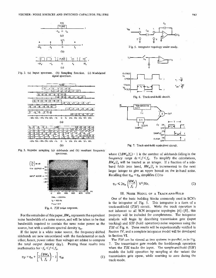
‘(’)+- ‘(’)’s(’)S(t)= ~8(t-kT)
Fig, 1. Ideal sampler.
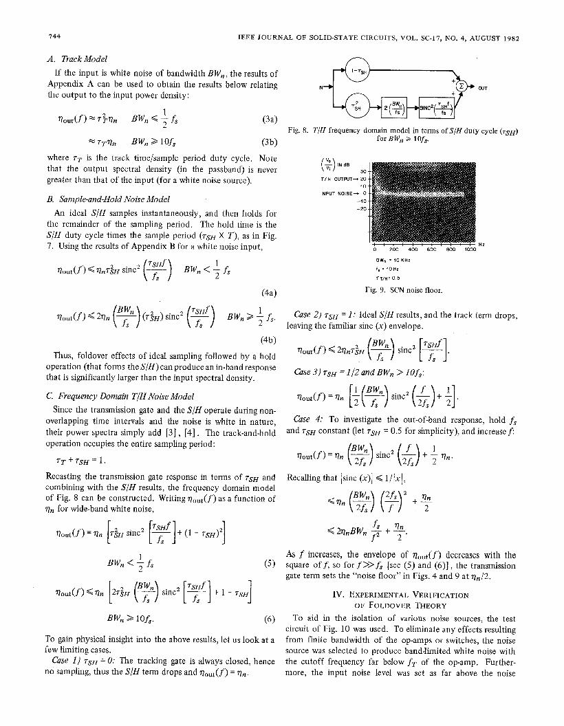
rate (f~). The baseband (~n) and sideband (~~b) spectraldensities of Fig. 2 are equal as a result of ideal impulse sampl-ing [4], [5]. A convention that will prove useful in the analysis
to follow is to number the sidebands so as to associate each
sideband with the sampling frequency harmonic it is centered
about, as in Fig. 2.For the more general case where the signal bandwidth is
greater than f~/2 (such as the output noise of an op-amp inan SCN), aliasing will occur. As an example, assume thatthe sigmd to be sampled has a bandwidth (Z3Wn) of three times
the sample rate. The first five sidebands resulting from thesampling operation have been depicted in Fig. 3(a). Referringto the figure, the following are contributors to the frequencyband from dc to f.: the fundamental, *1, +2, and the +3 side-bands. The addition of these sidebands is depicted in thestacked structure of Fig. 3(b). This spectral stacking of anundersampled signal results in an output of larger spectraldensity than the input for the frequency band from dc to f8/2.
The noise gain of a track-and-hold circuit is shown in Fig. 4(and is discussed in Section III).
0018 -9200/82/0800 -0742 $00.75 01982 IEEE
FISCHER: NOISE SOURCES AND SWITCHED CAPACITOR FILTERS 743
F(f)
I FUND /f
-fin o fin
(a)
-~ f
s a s
(b)
-2 -1 FuND +1 +2f
-2f, -f* o fs 2f,
(c)
Fig. 2. (a) Input spectrum. (b) Sampling function. (c) Modulatedsignal spectrum.
I FU,ND I ~-1 -i -4 -1 -4 -1 -1 -1 [
+3 ,+1 +1 +j +4 ,+1 ,+4 I 4-J-2 -2 -2 -2 -2 -2 -2-21
I +2 t2 +2 +2, +2 +2 +2 ~-
1-3 -3 -3 -3 -3’-3 -3 I1+3, +3, +3, +3. +3, ~.,. ,,
-4”-4’-4 -4 :4-4 II +4,+4 ,+4 ,+4 ,+.4 ,+4:
-5 -5 -5 -5 -5-51+5 +,5 +5, +5 +5 ,+5-
-6fs -5fs -4fs -3fs -2fs -fs O f: 2fs 3;s 4;s 5;s 6fs
(a)
~E-13 -8 -2 -2 -2 -2 -2 -2 -2 +4 +4 +4 +4 +4 &
-6fs -5fs -4fs -3fs -2fs -fs O fs 2fs 3fs 4fs 5fs 6fs
(b)
Fig. 3. Impulse sampling (a) sidebands and (b) resultant frequencyspectrum.
()Y IN dBY
T/H OUTPUT
INPUT NOISE
BWn = 400 KHz
f, = 100 Hz
TT,H= 0.5
Fig. 4. T)H noise response.
For the remainder of this paper, IllVn represents the equivalentnoise bandwidth of a noise source, and will be taken to be that
bandwidth required to contain the same noise power as thesource, but with a uniform spectral density rIn.
If the input is a white noise source, the frequency-shiftedsidebands are now uncorrelated with the fundamental or eachother; hence, power rather than voltages are added to computethe total output density (qT). Putting these results intomathematics for –.f~< .f< f~,
“=on+w?ws’ (1)
Fig. 5. Integrator topology under study.
“-+’mvo1-
b=!al-r-L, -~‘T ‘T
TRACK
‘%OLO ‘T “H t#T~
- ‘SH‘SH - ~
Fig. 6. Track-and-hold circuit.
OUT
+ T
SA~p$EAR CT ON
E-
tTOFF
_f_
ONSAMPLE
OFFtH4 t
—
CLEAR o: t—
Fig. 7. Track-and-hold equivalent circuit.
where (2BWn/f,) - 1 is the number of sidebands falling in thefrequency range dc < f < f.. To simplify the calculations,BWn/f, will be treated as an integer. If a fraction of a side-
band folds into band, BWn/f, is incremented to the nextlarger integer to give an upper bound on the in-band noise.
Recalling that ~,1, = qn simplifies (1) to
(2)
III. NOISE MODEL OF A TRACK-AND-H• L,D
One of the basic building blocks commonly used in SCN’Sis the integrator of Fig. 5. This integrator is a form of atrack-and-hold (T’/fI) circuit. While the track operation is
not inherent to all SCN integrator topologies [6] - [8], thisproperty will be included for completeness. The integrator
analysis will begin by describing transmission gate (inputtracking) and S/Ii (hold operation) noise responses using theT/H of Fig. 6. These results will be experimentally verified inSection IV, and a complete integrator model will be developedin Section VI.
The T/H can be viewed as two systems in parallel, as in Fig.
7, The transmission gate models the feedthrough operation
when the T/Ii tracks the input. The sample-and-hold (S/n)models the hold operation by sampling at the instant thetransmission gate opens, while resetting to zero during thetrack mode.
744 IEEE JOURNAL OF SOLID-STATE CIRCUITS, VOL. SC-17, NO, 4, AUGUST 1982
A. Track Model
If the input is white noise of bandwidth B Wn, the results of
Appendix A can be used to obtain the results below relating IN+
the output to the input power density:
noutm = ~% BWn <: f~ (3a)Fig. 8. T/H frequency domain model in terms of S/H duty cycle (.~H)
* TT~n BWn > 10f$ (3b) for Bwn > loffi
where t-~ is the track time/sample period duty cycle. Note
that the output spectral density (in the passband) is nevergreater than that of the input (for a white noise source).
B. Sample-and-Hold Noise Model
An ideal S/H samples instantaneously, and then holds forthe remainder of the sampling period. The hold time is theS/H duty cycle times the sample period (r~~ X T), as in Fig.
7. Using the results of Appendix B for a white noise input,
(,)%~ INdB
T/H OUTPUT+
INPUT NOISE -
Hz0 200 400 600 800 1000
()TSHfBW. = iO KHz
Tout(f) ~ mkk7 sinc2 — BW. < ; f.f.
f, = IOHZ
TT/H= 0.5
(4a) Fig. 9. SCN noise floor.
“ou’(f)<2”n(?)(T’H) sinc2 (%) ‘Wn>+fsCase 2) r~~ =l.’ Ideal S/H results, and the track term drops,
leaving the familiar sine (x) envelope.
(4b)
Thus, foldover effects of ideal sampling followed by a holdTout(f) < z’f?n~~fi (~)sincz[~].
operation (that forms the ~/~) can produce an in-band response
that is significantly larger than the input spectral density.case 3) TSH = 1/2 and BW. > 10f~:
C Frequency Domain T/H Noise Model ~out(f) =‘O. [X-%sinc’(ik)+lSince the transmission gate and the S/H operate during non-
overlapping time intervals and the noise is white in nature, Case 4: To investigate the out-of-band response, hold f8
their power spectra simply add [3], [4] . The track-and-hold and 7SH constant (let TSH = 0.5 for simplicity), and increase f:
operation occupies the entire sampling period:
rT+rsH=l.nout(fl=nn&)sinc2 (*)+~Vn.
Recasting the transmission gate response in terms of 7SH and Recalling that \sinc (x)1 < I/lxl,combining with the S/H results, the frequency domain model
of Fig. 8 can be constructed, Writing qout(f) as a function of~n for wide-band white noise, ‘“n(%) (%2
[2 2[%1+( ’-’4Vout(f) =~n TsH Smc
1 As f increases, the envelope of t?o~t(~) decreases with theBWn < + f$ (5) square of .f, so”for f >> f$ [see (5) and (6)], the transmission
gate term sets the “noise floor” in Figs. 4 and 9 at ~n/2.
[ 2 (i+in’z[%l-’d~out(f) ~ V. Z7SH IV. EXPERIMENTAL VERIFICATION
OF FOLDOVER THEORY
BWn > lof~. (6) To aid in the isolation of various noise sources, the test
circuit of Fig. 10 was used. To eliminate any effects resulting
To gain physical insight into the above results, let us look at a from finite bandwidth of the op-amps or switches, the noisefew limiting cases. source was selected to produce band-limited white noise with
Case 1) rs~ =0: The tracking gate is always closed, hence the cutoff frequency far below fT of the op-amp. Further-
no sampling, thus the S/H term drops and ~Out( f ) = Vn. more, the input noise level was set as far above the noise

FISCHER: NOISE SOURCES AND SWITCHED CAPACITOR FILTERS 74s
S*
WHITE NOISE +S4
GENERATOR
1 1
.
CLOCK 1$IOK
GENERATORI 1
w ‘CMOS(MG140666)TRANSMISSION GATE
Fig. 10. Transmission gate and S/H test circuit.
TABLE I(a) TRANSMISSIONGATENOISERESPONSEVERSUSDUTYCYCLE (f<< J)
FORBWn = 100 kHz AND ~, = 1 kHz. (b) S/H RESPONSE(f<< f,)FOR BWn = 100 kHz AND ~, = 1 kHz.
(a)
I 95 I o I -0.2 I
I61
I-1.8
I-2.1
50 -2.s -3.035 -4.2 -4.6 I1s -7.0 -7.45 -13 -13
(b)
Output referred to input First null frequency
Duty Cycle Measured Calculated Measured Calculated
(dB) (dB) (kHz) (kHz)
95 20 22.6 1.0 1.080 20 21 1.2 I .450 15 17 1.s 2.034 12 14 2.s 2.921 9 9.4 4.5 4.s11 4 3.8 8.8 9,15 -3 -3 19 20
floor as was practical without circuit limiting. The unstitched(switch latched in closed position) noise signal level serves asthe reference for all the results.
(Vo,)~ lNdB
INPUT
OUTPUT
I IN KHz
Fig. 11. Transmission gate wide-band input regponse.
(); INdE
OUTPUT
INPUT
f IN KHz01
.Z3456T 8940
BWn =IOOKH,
f,= 4 KHz
7$, ” =0.50
Fig. 12. S/H widbband input response.
TABLE HT/H CIRCUIT RESULTS (TSH = 50 PERCENT) FOR (a) Ill?’. = 100 kHz AND
(b) BWn = 10 kHz
(a)
f. Predicted Measured
Mdensity density
(Hz) (dB) (dB)lOOk -0.2 -210k 7.4 7.4lk 17 Is
100 27 29 z(Hz) (dB) (dB)10Ok -3 -3.810k o 1.5Ik 7.4 8.5
100 17 1710 21 26
A. Track Model Verification
Equation (3) indicates that the track noise contribution is
independent of noise bandwidth or sampIe rate (for BWn >10f~), and is dependent only on the track duty cycle. Thecalculated and measured track operation results are sum-marized in Table I(a) with the frequency independence shown
in Fig. 11.
B. S/HiVoise Model Verification
Using (4b) to predict the S/H response at dc (v~~a.) to a
wide-band input,
(–)BWn
‘“ma’ =2T;H f, ‘“”
For f~ = 1 kHz, BWn = 100 kHz, and rs~ = 0.5,
= 50qn (17 dB gain).
First null occurs at 1 kHz/O.5 = 2 kHz.The white noise response is shown in Fig. 12, with similarly
calculated and measured results summarized in Table I(b).
The S/H response extends below the input noise level because
the track operation, with its associated noise contribution, isnot present in the S/H.
C. T/H Noise Model Verification
To investigate the foldover term and the orthogonality of
the track and S/H operations, the T/H of Fig. 6 has beenutilized with a clock duty cycle of 0.5 (50 percent).
Sample Noise Calculation: Calculating the dc spectral densityfor the reduced sample rate off. = 100 Hz (measured response
in Fig. 4),
BWn = 100 kliz,f~ = 100 Hz.
Using (6),
= 500 (27 dB gain).
Similar results are to be found in Table II.

746 IEEE JOURNAL OF SOLID-STATE CIRCUITS, VOL. SC-17, NO. 4, AUGUST 1982
‘N”+l--m+izl--EOuTuT(a)
““$E1-HEH-EF+zl-O”l(b)
(c)
Fig. 13, Cascaded T/H’s with in-phase (a) and staggered (b) phaseclocking. The resampled wide-band noise spectrum for the staggeredclock case is shown in (c).
V. EXTENSION TO CASCADED STAGES
There are two extreme cases when cascading T/H stages.
One is when all the T/Hs have the same timing (in-phase
clocks) as in Fig. 13(a). The other extreme is when one T/Htracks, and the T/H before and after it are in the hold state
(staggered clocks) as in Fig. 13(b). While parts of an SCN
might contain both clocking schemes, SCN realization con-
siderations make the staggered clock case the most common
[6], [7], [11].
In one extreme, all the T/H stages are driven by the sameclock phases. Because the significant foldover effects are
present only in the hold phase (assuming a memoryless trackphase), the noise at the T/H input is simply the sum of the
unsampled noise feeding through to the stage of interest.
When the T/H changes to the hold phase, the input noise is
sampled and folded down to baseband. The resulting outputspectra are described by (5) and (6).
For the other extreme (staggered clocks), each successiveT/H samples the held output of the previous stage. This
sampling of a held output results in TSH = 1 and the output
spectrum of Fig. 13(c) where pb is the passband edge. It is
easily shown that the sin x/x envelope provides effective
anti-alias filtering of the folded noise (increasing with larger
f$/Pb ratios) so that resampling the held T/H output minimally
increases the in-band noise. As staggered T/H’s are cascaded,
the output noise of a given stage (in the hold phase) is closely
approximated by the resampled noise of the previous stages
added to the sampled wide-band noise of the stage the present
T/H is sampling.
In summary, since most SCN’S use staggered clocks, TSH will
be taken to be unity for the rest of the paper, and the effects
of resampling of noise will be ignored.
VI. SCN INTEGRATORS AND CHARGE ACCUMULATORS
In this section, a model of an SCN integrator is developed.The T/H results will then be combined with these results inSection VII where a simple SCN is analyzed.
+
(a)
%
Fig. 14. (a) Charge accumulator and (b) simplified accumulator withV~ngrounded.
The topology of the charge accumulator (with the l/~ andflatband op-amp noise modeled by F’n) of Fig. 14 is represen-tative of a basic structure used in SCN filters [6] - [8], so acareful analysis is in order.
A. ChargeAccumulator Model
To aid in visualization, the accumulator is redrawn in Fig.14(b) with Vk grounded. Assume as initial conditions that
qcr = qc~ = O and that the op-amp voltage gain is infinite.After switch SI has closed, the feedback action of CI will
force the output to
()Vo= 1+% Vn
(while driving the inverting input to equal Vn) and to track Vn
with gain thereafter. The transient resulting from C7Rcharging
to V. does not trap charge on CI because only the trapped
charge from previous sample periods will remain if the ampli-
tude of Vn returns to zero at the instant 111 opens. The
additional charge trapped on CI at the instant ~1 opens (at
time tl) is
AqcI(tl) = qCR = CR Un(tl)
with
Avcl(tl) = ~ Vn(tl).
With S2 closed and SI open, qc~ is bled off to ground, andP’. tracks Vm with unity gain and a dc offset equal to the
voltage stored on CI. When Sz opens and S1 closes, the in-verting terminal is initially pulled to ground, and the op-ampthen recharges CR to P’n, repeating the above procedure. Note
that the only time charge is trapped on CI is when S1 opens,
resulting in an accumulated output offset ( Vnet) of
Vnet . ‘y ~ V.(iT)i=1
(7)

FISCHER: NOISE SOURCES AND SWITCHED CAPACITOR FILTERS 747
““+”0Fig. 15. SCN inte~ator noise model for CR/CI <<1 and Requ =
l/cRf~
where J’n(iT) is the noise voltage at the instant S1 opens, Tis the complete SI, S2 period, and N is the number of com-
plete clock periods since Cl was discharged. The output
when S’l is closed is
()~o. ,+%C*
Vn(t)+ vne*(N- 1).
When S2 is closed,
(8)
V.= Vn(t) + Vne(fv) (9)
where the index of Vnet has been incremented because addi-
tional charge has been trapped on C[ when S’l opened.
If there are N sample periods per clearing of CI (as in some
low-loss integration techniques), and Vn is Gaussian white
noise, probability theory indicates that Vnet(N) will have a
standard deviation {N times larger than (CR /Cz) Vn. In other
words, the noise power of Vnet after ~ cycles will be Al times
larger than the incremental noise power stored on CI in any
given sample cycle.
B. SCN Filter Approximations
A significant simplification can be made for those filterstages with pole frequencies much less than the sample rate.These filters usually have CR /CI <<1. Under these conditions,(7) shows that the individual contributions to Vnet are lessthan the referred to input noise Vn by CR /Cz. In addition,the number of terms in (7) that significantly contribute to theintegrator’s output noise is limited by dc discharge paths from
the amplifier output to its input. These discharge paths are
used to provide Q damping and dc stability of the filter. Inmost practical SCN’S, these conditions result in the inputreferred noise of the op-amp ( Vn) being much larger than Vnet,
so the J&t term will be dropped.To model charge transfer uncertainty and the foldover effects
of the wide-band noise of the switches associated with CR, anequivalent resistance of value [9]
1R =—
‘q” cRf,
is used in the continuous-time equivalent circuit of Fig. 15.These approximations hold when the fflter passband is muchless than the sample rate. For the noise simulations of the nextsection, the SCN integrator will be replaced by its continuous-time counterpart. The output noise of a particular SCN willbe worked out in detail in Section VII to demonstrate how touse these results.
Fig. 16. HPN noise test chcuit.
R3
I C4 R, I
II 1~
c~ ‘NON-INVERTINGINTEGRATOR
Fig. 17. Noise simulation model for HPN SCN.
VII. NOISE MODEL AND CALCULATIONS FOR SCN’S
This section will develop a model suitable for SPICE noisesimulations of switched capacitor networks. Experimentalresults in support of these results will also be given.
A, SCN Topology Model
To simulate the capacitor switching noise (kT/C), replace
the switched capacitors of the HPN in Fig. 16 with resistors
of value
R.~Cf,
as per Fig. 17.Next replace the op-amps with the blocks shown in Fig. 17.
The switched output (S.) is connected to all the switchedcapacitors connected to the output of the op-amps. The con-
tinuous output (CO) is connected to the paths that are not
switched. To model the noninverting integrator of Fig. 16,use a voltage-controlled voltage source of gain = -1 to provide
the polarity reversal (as in Fig. 17). The filter topology hasnow been modeled; next the op-amp model will be developed.
B. Op-Amp Model
To model the op-amp of Fig, 18 in an SCN environment,the sampled data effects on the output noise of the op-ampmust be considered. This noise consists of two parts: wide-
band (flat, white noise), and ‘l/f (flicker) noise. The voltagesources Vl,f and Vnl are used to model the unsampled l/fand flat-band noise, respectively. Since the folciover effectsare added to the unsampled output noise, the noise sourceskVnll and Vfll have been placed in series with the continuousoutput to yield SO. Referring to Appendix C to determine theop-amp BWn, the foldover factor (k) is derived by simplifying(6) under the constraints that .f<<.f., so the sin x/x term
748 IEEE JOURNAL OF SOLID-STATE CIRCUITS, VOL. SC-17, NO. 4, AUGUST 1982
IN
Fco+
so‘N, ‘F1l kV
‘I?
v1/f
v,/f (f) = ~ v,,, = J-=
=
INco
so
IvN,,/rms ‘Ivfijm ,oLDOv,R F/as,BUT UNCORRELATED, USED TO MODEL
co OUTPUT TO NON-SAMPLED PATHS
So OUTPUT TO SAMPLEO PATHS
Fig. 18. Frequency domain SCN op-amp noise simulation model.
approaches unity and 7SH = 1. Then separate the result intoterms related to the CO and SO outputs, respectively:
[1
2BWnVout(f) ~ % +v. —
f. ‘1
with the bracketed term representing the foldover effectsrepresented by lcVnll . Similarly accounting for the l/~ con-
tribution (Appendix C),
nl/f out(f) Q $ + (d).
Because programs such as SPICE work with noise voltagesrather than powers, the noise voltage gain through samplingis obtained by taking the square root of the bracketed termsto yield
k.
i
2BWn—-1
f,
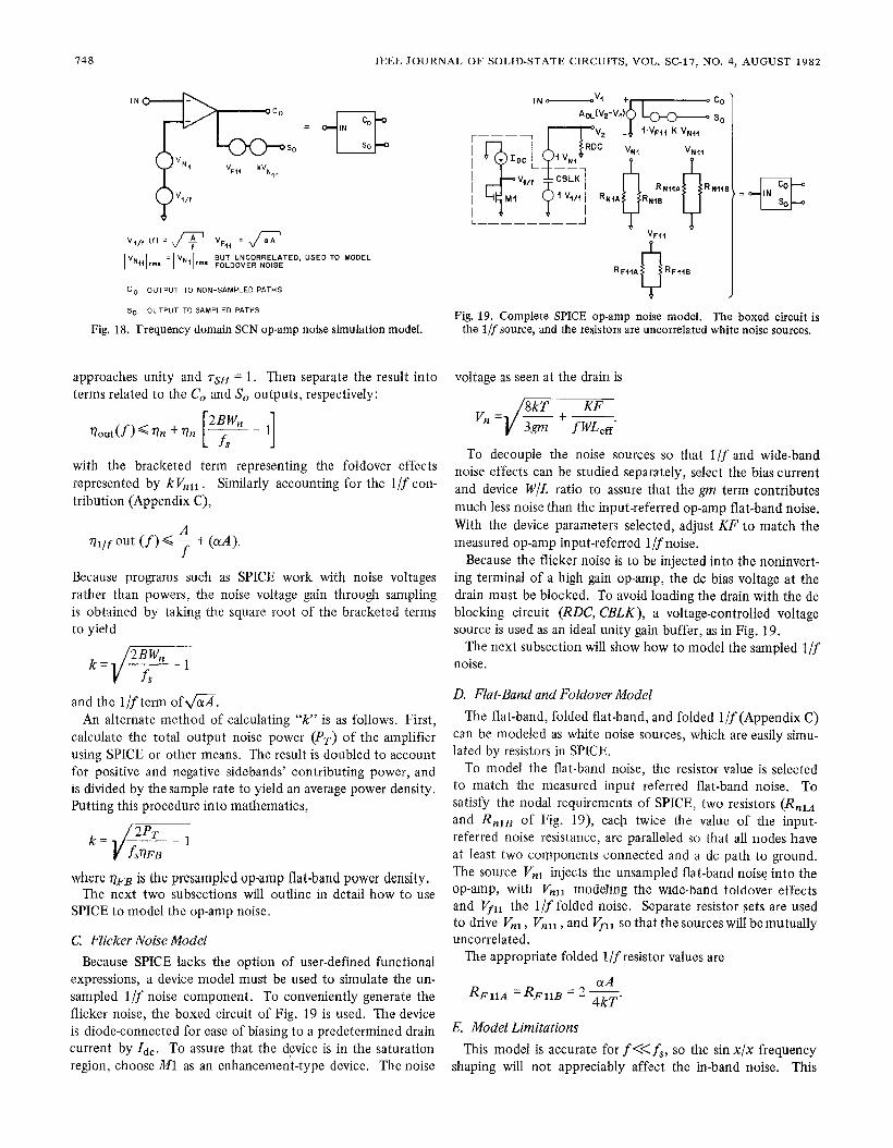
and the 1/f term [email protected] alternate method of calculating “k” is as follows. First,
calculate the total output noise power (PT) of the amplifierusing SPICE or other means. The result is doubled to accountfor positive and negative sidebands’ contributing power, andis divided by the sample rate to yield an average power density.Putting this procedure into mathematics,
where T/FBis the presampled op-amp flat-band power density,The next two subsections will outline in detail how to use
SPICE to model the op-amp noise.
C. Flicker Noise Model
Because SPICE lacks the option of user-defined functionalexpressions, a device model must be used to simulate the un-
sampled 1/f noise component. To conveniently generate theflicker noise, the boxed circuit of Fig. 19 is used. The deviceis diode-connected for ease of biasing to a predetermined draincurrent by ~&. To assure that the device is in the saturationregion, choose Ml as an enhancement-type device. The noise
v~,,
? I
R ~f,.
#
RF44B
Fig. 19. Complete SPICE op-amp noise model. The boxed circuit isthe I/f source, md the resistors are uncorrelated white noise sources.
voltage as seen at the drain is
‘n=is=%To decouple the noise sources so that 1/f and wide-band
noise effects can be studied separately, select the bias current
and device W/L ratio to assure that the gm term contributes
much less noise than the input-referred op-amp flat-band noise.
With the device parameters selected, adjust KF to match the
measured op-amp input-referred 1/f noise.
Because the flicker noise is to be injected into the noninvert-
ing terminal of a high gain op-amp, the dc bias voltage at the
drain must be blocked. To avoid loading the drain with the dc
blocking circuit (l?llc, CBLK), a voltage-controlled voltagesource is used as an ideal unity gain buffer, as in Fig. 19.
The next subsection will show how to model the sampled I/fnoise.
D. Flat-Band and Foldover Model
The flat-band, folded flat-band, and folded 1/f (Appendix C)can be modeled as white noise sources, which are easily simu-lated by resistors in SPICE.
To model the flat-band noise, the resistor value is selectedto match the measured input referred flat-band noise. Tosatisfy the nodal requirements of SPICE, two resistors (Rnl~and I?nlB of Fig. 19), eac~ twice the value of the input-referred noise resistance, are paralleled so that all nodes have
at least two components connected and a dc path to ground.The source Vnl injects the unsampled flat-band noise into the
op-amp, with Vnll modeling the wide-band foldover effectsand V’jll the 1/f folded noise. Separate resistor sets are usedto drive Vnl, Vnll, and V’ll so that the sources will be mutually
uncorrelated.
The appropriate folded I/f resistor values are
E. Model Limitations
This model is accurate for f << f~, so the sin x/x frequencyshaping will not appreciably affect the in-band noise. This

FISCHER: NOISE SOURCES AND SWITCHED CAPACITOR FILTERS
TABLE IIIMONOLITHICFILTER RESULTS. NOISEVOLTAGES ARE rms VALUESINTEGRATED
OVERTHEFREQUENCYRANGEFROM1 Hz TO10 kHz.
FILTER I/f FLAT CAPACITOR:.:; dihc”MEASURED
dBrncHPN 4.V 6.5.. 9.0””1 12””
J, = 8kH,-6.5 -6
HPN4.. 3.9”” 4.1.”?
/s+4kHz6.81N -11 -8
LPF 12“. 25UVfs-128kHz
45.”3 531N 6.7 8.5
LPF
reduced 12UV 25U” 100”V* 11o“” 13 15caps.
LPFreduced 27UV 25UVcaps.&
100UV4 11OW 13 16
inputdcv.
“ O dBrn (24.5.v)
‘ CM = 0.6PF1 Cw = 0.3rJF
1 C.m = L7pF4 C.w = o.3pF
constraint is not severe since most SCN’S are designed withthe sample rate much greater than the passband frequency.Further assumptio~s made to simplify the calculations are
that the hold duty cycle of the switched paths (7sH) is unity
and that the filter is run at a single sample rate. If stages of
differing sample rates are cascaded, the sampled noise spectra
of previous stages must be analyzed to account for significantfoldover contributions to the stage under consideration.
F. Gdcutation and Measurement Results
Using models like the above, SPICE simulations were used
to calculate the output noise for 60 Hz F@N filters sampledat 8 and 64 kHz, and several 128 kHz sample rate fifth-orderelliptic low-pass filters with a cutoff frequency of 3.4 kHz
[8]. The calculated C-message weighted (dBrnc) noise resultsare summarized in Table III, and are compared to results ob-tained from monolithic realizations of these circuits. Theop-amp noise was measured to be 50 nV/ @ at 1 kHz, witha flat-band noise component of 35 nV/ @ and a noise band-width of 2 MHz.
Fig. 16 shows an actual HPN (sampling at 8 kHz) switched
capacitor filter [8], and its complete noise model is shown inFig, 17, Calculating k for the filter with op-amps having a
noise bandwidth (see Appendix C) of 2 MHz,
‘=FT5=-=223Referring to Table V indicates that a = 2.1 for this samplerate.
The dominant noise term of the HPN is the capacitor switch-ing noise. If the falter is followed by an 8 kHz S/H, the wide-
band noise of the second amplifier will be boosted by the fold-over factor (22.3) to become the dominant contributor.
Similarly, the dominant noise source in the LPF’s is the capac-itor switching noise.
The measured and predicted noise spectra are compared inFig. 20 for the 1.7 pF minimum capacitor size LPF. If wide-band noise sources are the dominant terms of the LPF, the
noise density should drop by 9 dB for a factor af 8 increase
-410 I 1 1 1 I 1
I , I I 1 I I J
o 2K 4K 6K . 8K 10K
f IN HZ
Fig. 20. Measured versus calculated 1.7 pF unit capacitor LPFresponse.
-80
–90
-400
-420
—L ! 1 I I 1
0 2 4 6 8 10
I , 1 , 1 i 1 , i I
o 46 32 40 64 80
f IN KHz
749
noise
Fig. 21. Measured noise response of the 1.7 pF unit capacitor LPF forfs =128MZ (top trace) and for f$ =1024 kHz (bottom trace). Allanalyzer settings are the same for both traces except that the lowertrace stop frequency (80 kHz) is eight times that of the top trace(10 kHz).
in sample rate. As a test, the noise responses for ~~ = 128 and1024 kHz of this LPF are compared in Fig. 21. All the analyzer
settings are the same for both traces, with the exception thatthe frequency sweep was changed from 10 ,Wz up to 80 kHz[for ~~ = 1024 kHz) so the re~ative densities can be directlycompared. The approximate 10 dB drop in the passband noisedensity clearly indicates that 1/f noise is definitely not thedominant noise source of these filters.
VIII. CONCLUSION
The results presented show that the topology of an SCN
determines the significance of the relative contributions ofamplifier flat-band and 1/f, and capacitor switching noise tothe overall filter noise, For the test chip filter designs in ourprocess, the dominant noise source was found to be capacitorswitching noise, followed by op-amp wide-band noise, andlastly, op-amp 1/f noise. A noise model and a simulation
technique have been develcrped to allow existing simulationprograms (such as SPICE) to be used in accurate SCN noise
calculations.
APPENDIX A
Transmission Gate Noise Mod@
The transmission gate simply m~dulates the input signal{x(t)}by a pulse train, as shown in Fig. 22. The Fourier

750 IEEE JOURNAL OF SOLID-STATE CIRCUITS, VOL. SC-17, NO. 4, AUGUST 1982
x(t)
--P~_y(+) . ‘(+) x Y(t) =x(t) f(t)
‘(’) rl.--.ro TT T
Fig. 22. Transmission gate model.
TABLE IVTRANSMISS1ONGATENOISE RESPONSEAS A FUNCTIONOF DUTY
CYCLE AND B WJf,
)UTY CYCLE
T
1.00
095
0 so
O 60
0,50
035
020
010
0.05
0
100
1.00
0.95
0 so
O 60
0.50
0.35
020
010
0049
0
/vowv.
B Wnas a function of ~
10
I 00
094
079
0.59
0.49
034
019
0.090
0.040
0
6
I .00
0.93
0 7s
059
0.4s
033
018
0 0S6
0.029
0
J.
1
I .00
091
071
054
0.45
0.2s
011
0029
0007
0
“ (fdd.v.r eiTccts absent)
series of the modulating pulse is
(- ~)i
f(t)=T+; -g— ()i 27rtsin (i7rr)cos —
i=~ i T
1Y2‘
1,00
0.90
064
037
0.25
012
0.04
0.010
0003
0
(Al)
where ~ is the duty cycle and T is the sample period. Working
out the details for a white noise input of bandwidth BWn,
[21F)’H+in(i+’] ‘A2’%tlt(.f)=n’. T + j ~
where h = BWn/j_~ (number of positive sidebands falling inband).
Since (A2) is not in a convenient form for h, qout(~) has beentabulated in Table IV for various BWn /f~ and ~. An importantapproximation can be made for h >10:
B W.%Nlt(f)= w’?? — >10,
‘or f,(A3)
while at the other extreme, h = O (sin’ terms are not present),
%ut(f) = ~’% for 2BWn <f8. (A4)
APPENDIx B
A Sample-and-Hold Noise Model
A general topology for a discrete-time data system is shown
in Fig. 23. The sampling function is shown in Fig. 24. TheS/H operation consists of ideal sampling, followed by filteringwith H(z) = 1, feeding into a hold operation. The hold re-
X(t) J
T [x,]Y(t)
L___J L~lzll~J [Ynl L-__JSAMPLING RECONSTRUCTIONOPERATION TRANSFER FILTER
FUNCTION
Fig. 23. General topology of a sampled data system.
x(t)[h]
%“+–+’’f’’,~po
INPuT SAMPLER SAMPLED DATAOUTPUT
Fig. 24. Ideal sampling switch operation.
h T
Fig. 25. Ideal S/H impulse response.
constructs the impulse train into a series of levels which con-
stitute the familiar held output response.
Calculation of {x.} Spectrum
Taking the Fourier transform of {xn} [10], we find
[1X(ej2”fT) = + ~ X“ 27rf+*k- co
(Bl)
where Xa is the Fourier transform of x(t), which is periodic
about multiples of the sampling frequency.
Calculation of the S/H Frequency Response
Referring to the timing of Fig. 25, we can determine the
limits of integration:
.Jf=_m Jt=o
= he-j2rf(k/2) sine (flz)
where
sin (rrx)sine (x) = ~x
h = (hold duty cycle) (sample period)
Substitution yields
[01G(2nf ) =rT sine r Kf.
e-iznf(hlz) . (B2)
When dealing with noise, power is usually the quantity of
interest; calculating the output spectrum,
]Y(2flf)12 = ]X(ej2nfT) G(27rf)[2 = ]X(ej2TfT)[2 ]G(2nf)[2.

FISCHER: NOISESOURCES AND SWITCHED CAPACITOR FILTERS 751
Calculating lX(ei2zfT)12,
For the case at hand, x(f) is white noise; hence, the aliases
are uncorrelated, with the result that power, rather thanvoltage, terms are added. Using (2),
()lX(e~2”fT)12 ‘ + r?. ~ for f, G 2BWn (B3a)
1“l?n~ for f,> 2BWn, (B3b)
and for the S/H,
[01]W)12‘r2T2 sinc2 r ~ .f.
(B4)
Combining (B3) and (4) yields
Jy(f’J2=2w%2sinc2 [’(;)1‘s<2Bwn(B5a)
and
[()1Iy(f)l’ =?7n72 sinc2 I-~ f.> 2BWn. (B5b)
The usual application of sampled data systems is the processing
of information in the passband (f< f~/2); accordingly, the in-
band signal-to-noise ratio is of interest. Since signal-to-noise
is given by
s _ Iinput (2nf)12 [G(2nf)]2 Iinput (2mf)12
X - ]X(ej2TfT)[2 lG(27rf)12 = ]X(ei2nfT)]2 ‘
it is independent of the reconstruction filter in the passbandfor white noise input, but does depend on the undersamplingof noise.
APPENDIX C
Foldover Effects and Equivalent Noise Bandwidth
This analysis will treat the op-amp 1/f and wide-band noiseseparately to clearly show the different effects of undersampling
of these noise sources and to point out useful approximations.
Wide-BandNoise
Fig. 26 depicts a characteristic voltage-follower output noise
spectrum (of the wide-band component only) that has beendivided into frequency bands of width f,. Settling time con-straints of SCN’S usually restrict f~ to be much less than theop-amp unity gain frequency. Additionally, the switch band-
widths are usually set much wider than that of the op-amp.With the wide-bandwidth switches, effectively all the outputnoise of the op-amp is folded back in to the baseband from dc
OUTPUTNOISE
DENSITY II
Fig, 26. Voltagefoltower output noise spectrum with test configuration.
h
~f- fs -fof fs
Fig. 27. Fundamental and fust two sidebands of a sampled I/f noisesource.
to f.. The total op-amp output noise is calculated by adding
up the power in each frequency band of width f~,
The equivalent noise bandwidth (BWn) of an op-amp will
be taken to be that bandwidth required to contain the same
noise power as the op-amp, but with a uniform spectral
density qn.
I/f Foldover Effects
Idealized sampling of a 1/f noise source produces the spectrum
of Fig. 27 where only the first sidebands have been shown for
simplicity, In the analysis that follows, it is assumed that the
noise spectral density follows an ampl~ude envelope of the
form A/f, and that the sidebands are mutually uncorrelated
so that power, rather that voltage, is summed.Evaluating the foldover effects in the baseband from dc to fs,
(cl)
where N is the number of sidebands folding into the baseband.
To understand the foldover effects described in (Cl), let us
assume that the voltage-follower op-amp attenuates the l/f
noise for frequencies above 20 MHz, A = 1000 for computation
ease, and that the frequency range of interest is the familiartelephone voiceband from 300 to 4 kHz. Fig. 28 comparesthe presampled and postsampled spectra for several commonclock rates. An important aspect of Fig. 28 is that all the
process dependence is lumped into the constant A, so these
curves are simply multiplied by the same scale factor to fit
any process. Evaluating just the foldover terms of (Cl) (and
calling that sum a) indicates that the 1/f foldover effects canbe closely approximated by adding a constant to the pre-sampled spectrum. Also note that for typical sample rates of
64 kHz or higher, the foldover contribution is less than 20percent of the 1/f baseband density at 1 kHz. A simplifyingapproximation is to neglect the 1/f foldover term entirely fora sample rate of 100 kHz or higher. For lower sample rates,

752 IEEE JOURNAL OF SOJ.ID-STATE CIRCUITS, VOL. SC-17, NO. 4, AUGUST 1982
7,,,
0 400 iK 4OK
f IN Hz
Fig. 28. Pre- and postsampled l/~ spectra for several sample rates. FOI these curves, V~/f =A/f with A = 1000.
TABLE V [5]1/y FOLDOVER FACTOR IN UNITS OF HZ-l
rfil. L-,
(Jz)f, = 8kHz 16kHz 32kHz 64Hz 12SkHz 256kHz
300 2.1 0.96 0.44 0.20 0.09 0.041000 2.1 0.96 0.44 0.20 0.09 0.042000 2.1 0.97 0.44 0.20 0.09 0,04
[7]
3000 2.2 0.97 0.44 0.20 0.09 0.043500 2.2 0.97 0.44 0.20 0.09 0.044000 2.2 0.97 0.44 0.20 0.09 0.04 [8]
place a white noise source in series with the sampled op-amp [9]
output (Fig. 16) of magnitude cd as summarized in Table V.[10]
ACKNOWLEDGMENT
The author is grateful to P. E. Fleischer, A. Ganesan, D. G.[11]
Marsh, and K. R. Laker for their helpful discussions and ideas.Special thanks go to A. A. Schwarz for the excellent layoutand laboratory work performed.
[1]
[2]
[3]
[4]
REFERENCES
C.-A. Gobet and A. Knob, “Noise analysis of switched capacitornetworks,” in ISCAS Proc., Apr. 1981, pp. 856-859.B. Furrer and W. Guggenbuhl, “Noise analysis of sampled-datacircuits, “ in ISCASF%oc., Apr. 1981, pp. 860-863.M. L. Llou and Y-L. Kuo, “Exact analysis of switched capacitorcircuits with arbitrary inputs,” IEEE Trans. Circuits Syst., vol.CAS-26, pp. 213-223, API. 1979.A. B. Carlson, Communication Systems. New York: McGraw-Hill, 1968.
R. A. Gable and R. A. Roberts, Signals and Linear Systems.New York: Wiley, 1973.G. M, Jacobs, “Practical design considerations for MOS switchedcapacitor ladder ffiters,” Electron. Res. Lab., Univ. California,Berkeley, Memo. UCB/ERL M77/69, Nov. 1977.D. J. Allstot, “MOS switched capacitor ladder filters,” Ph.D.dissertation, Electron. Res. Lab., Univ. California, Berkeley,Memo. UCB/ERL M79/30, May 1979.P. E. Fleischer and K. R. Laker, “A family of active switchedcapacitor biquad building blocks,” Bell Syst. Tech. J., vol. 58,pp. 2235-2269, Dec. 1979.C.-A. Gobet and A. Knob, “Noise generated in switched capacitornetworks,” IEE Electron. Lett., vol. 16, pp. 734-735, Sept.1980.A. Peled and B. Liu, Digital Signal Processing. New York: Wiley,1976.P. E. Fleischer, A. Ganesan, and K. R. Laker, “Effects of finiteop amp gain and band-width on switched capacitor falters,”presented at the IEEE Int. Symp. Circuits and Syst., Apr. 1981.
Jonathan H. Fischer received the B.S. and M.S.degrees in electrical engineering from the Univer-sity of Colorado, Boulder, and the Universityof California, Berkeley, in 1978 and 1979,respectively.
In 1978 he joined Bell Laboratories, Holmdel,NJ, as a member of the Technical Staff. Sincethen he has been involved in various aspects ofcharge-redistribution codec and filter work.