non-ideal behavior of feedback amplifiers dc errors … · non-ideal behavior of feedback...
TRANSCRIPT

Copyright 2014 Tim J. Sobering
Operational Amplifiers: Part 2
Non-ideal Behavior of Feedback AmplifiersDC Errors and Large-Signal Operation
by
Tim J. Sobering
Analog Design Engineer& Op Amp Addict

Summary of Ideal Op Amp Assumptions
Zero input offset voltage (Vos) Zero input bias current (IBias ,IBias‐) Infinite slew rate
Infinite large-signal (or full-power) bandwidth
Infinite output drive No voltage rail limits Zero output impedance (Zo) Infinite input impedance (Zi) Infinite small-signal bandwidth Infinite open-loop gain (Av)
Actually, infinite gain for a differential input, zero gain for a common mode input
Copyright 2014 Tim J. Sobering

Op Amp Internals – TLV2721C (just for fun)
Copyright 2014 Tim J. Sobering

Op Amp Internals – TLV2721C (just for fun)
Copyright 2014 Tim J. Sobering

Copyright 2014 Tim J. Sobering
DC Errors

Input Offset Voltage
Input Offset Voltage is the voltage that must be applied to the input to make the output equal to zero volts Polarity is not predictable as it is a manufacturing variance
Vos ranges from a few µV to typ. around 5mV Chopper-stabilized are lowest 1 µV “Precision” Op Amps have low Vos Untrimmed CMOS amps can reach 50mV
Vos will drift with temperature and time As low as 0.1 µV/°C,typically1– 10µV/°C Aging is proportional to the square root of time
1µV/1000hr→ 3 µV/year (9000 hours)
Error due to Input Offset Voltage can be very large in Instrumentation Amplifiers
Copyright 2014 Tim J. Sobering
TVL2721 Spec:0.5 mV typ, 3 mV max.

Errors resulting from Input Offset Voltage
Modeled as a voltage source in series with the inverting terminal
Note: Inverting or Non-inverting result is the same
00
1
1
Copyright 2014 Tim J. Sobering
+
-
OUT
RfRg
V_OUT
VOS
VosNoiseGain(NG)
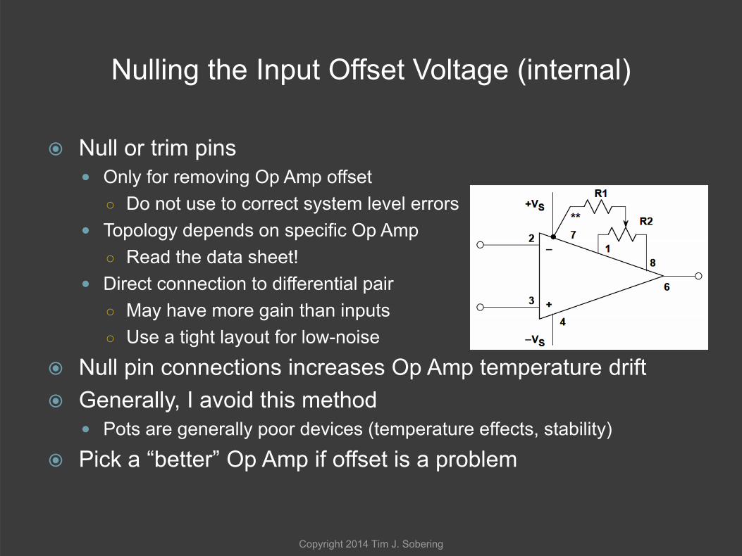
Nulling the Input Offset Voltage (internal)
Null or trim pins Only for removing Op Amp offset
Do not use to correct system level errors Topology depends on specific Op Amp
Read the data sheet! Direct connection to differential pair
May have more gain than inputs Use a tight layout for low-noise
Null pin connections increases Op Amp temperature drift Generally, I avoid this method
Pots are generally poor devices (temperature effects, stability)
Pick a “better” Op Amp if offset is a problem
Copyright 2014 Tim J. Sobering

Nulling the Input Offset Voltage (external)Inverting amplifier
Use a reference voltage (or a DAC), not the supply
Copyright 2014 Tim J. Sobering
Preferred
A cap here can reduce added noise
Assumes R3 + RA||RB >> RP
Assumes R3 >> RA||RB

Nulling the Input Offset Voltage (external)Non-inverting amplifier
Pick components to minimize change in noise gain Pot/Reference can always be replaced by a DAC
Copyright 2014 Tim J. Sobering
(Keeps pot from changing gain)

Input Bias Current
As low as 60fA to several µA Very variable Inputs can be well-matched…or not Can be stable with temperature or may double every 10°C May flow in or out and can change direction with CM voltage
Depends on input structure and internal cancellation circuits
Don’t assume that both inputs currents flow the same direction Look at Input Offset Current specification
Ios is the difference between Ibias and Ibias– If Ios << Ibias currents probably flow the same direction Ios is meaningless for current feedback amplifiers
Pick a “better” opampCopyright 2014 Tim J. Sobering
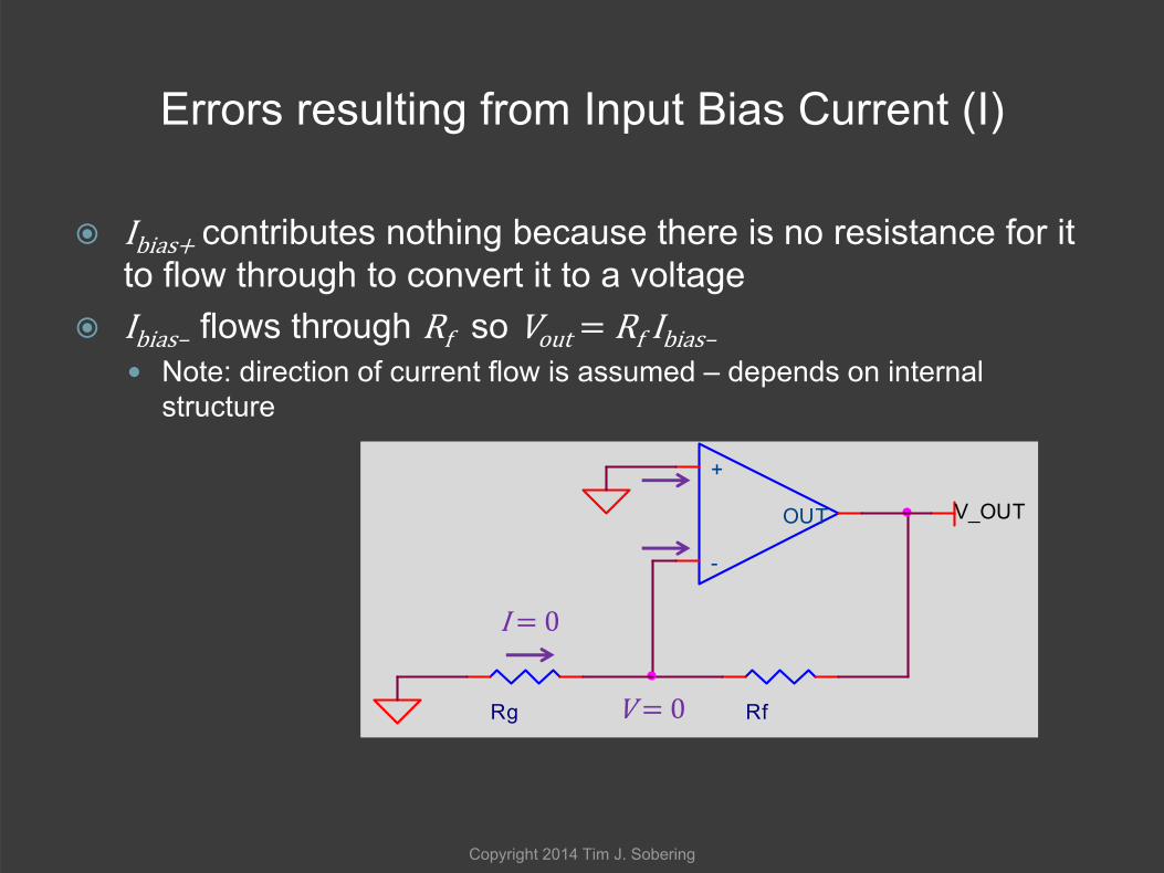
Errors resulting from Input Bias Current (I)
Ibias contributes nothing because there is no resistance for it to flow through to convert it to a voltage
Ibias– flows through Rf so Vout Rf Ibias– Note: direction of current flow is assumed – depends on internal
structure
Copyright 2014 Tim J. Sobering
+
-
OUT
RfRg
V_OUT
I 0
V 0
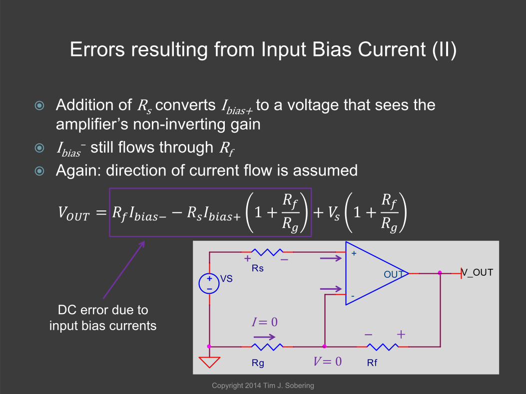
Errors resulting from Input Bias Current (II)
Addition of Rs converts Ibias to a voltage that sees the amplifier’s non-inverting gain
Ibias– still flows through Rf Again: direction of current flow is assumed
1 1
Copyright 2014 Tim J. Sobering
VSRs
+
-
OUT
RfRg
V_OUT
I 0
V 0
–
+ –
DC error due to input bias currents

Watch out for AC coupled circuits
Op Amp inputs must have a DC part to ground Applies to Instrumentation amps too!
Without R, non-inverting node will drift until Vout saturates For polarity shown, output will go to the negative rail Time required: dV/dt Ibias /C
Copyright 2014 Tim J. Sobering
VS
+
-
OUT
Rf
V_OUT
Rg
C
R
This resistor is critical
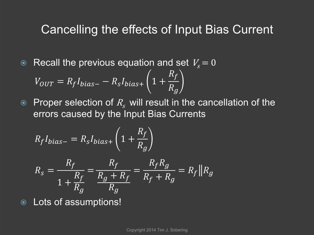
Cancelling the effects of Input Bias Current
Recall the previous equation and set Vs 0
1
Proper selection of Rs will result in the cancellation of the errors caused by the Input Bias Currents
1
1
Lots of assumptions!
Copyright 2014 Tim J. Sobering

Requirements for Input Bias Current Cancellation
Cancellation technique only works when Input Bias Currents are well matched Ibias and Ibias– must be (nearly) equal and flow in the same direction
Key is to look at the Input Offset Current specification Input Offset Current must be << Input Bias Current
Op Amps with internal bias current compensation have Ios Ibias Watch out for Rail-to-rail Op Amps
Direction can change with common-mode voltage
If not well matched, this technique makes the error worse If you don’t know what you are doing…don’t try designing it
Or build the circuit and learn something!
Copyright 2014 Tim J. Sobering
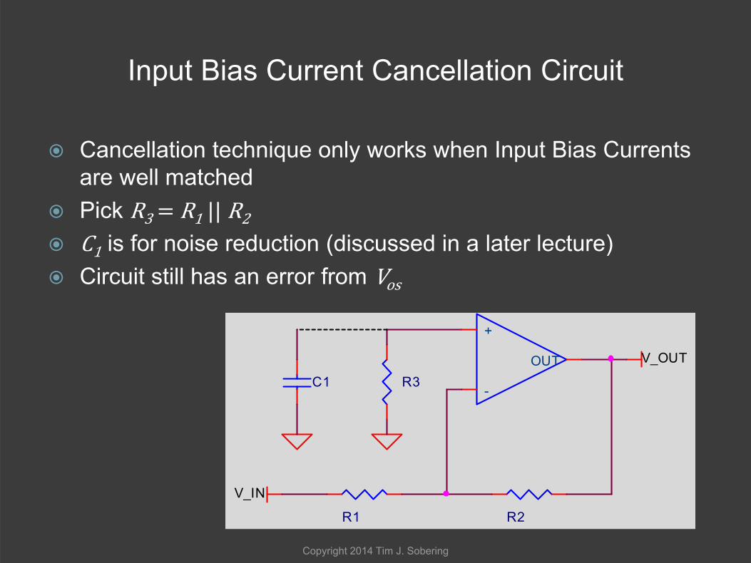
Input Bias Current Cancellation Circuit
Cancellation technique only works when Input Bias Currents are well matched
Pick R3 R1 ||R2 C1 is for noise reduction (discussed in a later lecture) Circuit still has an error from Vos
Copyright 2014 Tim J. Sobering
R1
V_OUT
V_IN
R3C1
+
-
OUT
R2

Output Drive
Op Amp output swing is limited by load Most Op Amps can output 10 mA
If you need more, look closely at specs or add a current booster
Greater loading can change performance Increased distortion Higher temperature (due to power dissipation)
Copyright 2014 Tim J. Sobering
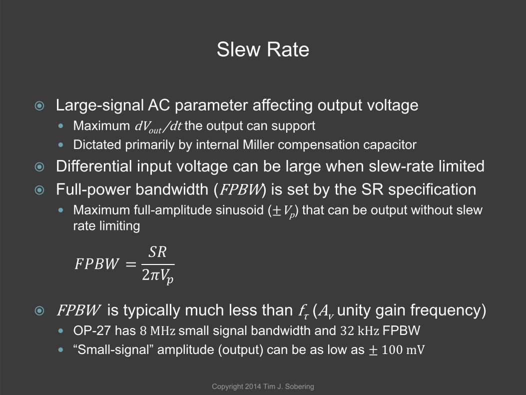
Slew Rate
Large-signal AC parameter affecting output voltage Maximum dVout /dt the output can support Dictated primarily by internal Miller compensation capacitor
Differential input voltage can be large when slew-rate limited Full-power bandwidth (FPBW) is set by the SR specification
Maximum full-amplitude sinusoid ( Vp) that can be output without slew rate limiting
2
FPBW is typically much less than fτ (Av unity gain frequency) OP-27 has 8MHzsmall signal bandwidth and 32kHzFPBW “Small-signal” amplitude (output) can be as low as 100mV
Copyright 2014 Tim J. Sobering

Input and Output Impedance
Op Amp input impedance is typically a large resistance in parallel with a small capacitance 105 – 1012 Ω || 3 – 25 pF CM impedance is from each input to ground DM impedance is between inputs BJT input stages typically have lower capacitance CM input voltage can modulate input capacitance in non-inverting
amplifiers and cause distortion
Op Amp output impedance is typically treated as a resistance 10 – 100 Ω is typical, can be 1 kΩ Reduced by 1 Avβ ‐1 in closed loop designs Can be an issue at high frequencies when Avβ craps out Can be an issue with capacitive loads
Copyright 2014 Tim J. Sobering

Input and Output Common Mode Range
Input Common Mode Voltage is defined as:
2
More important is the input and output common mode range The common-mode range is specified w.r.t the supply voltage Defines how close the input or output can get to the rail before
saturating
Watch out for rail-to-rail Last 50 mV is often nonlinear
Single supply design!
Copyright 2014 Tim J. Sobering

Interesting Common Mode Issue
Op Amps have differential mode and common mode gain High DM Gain (Av) Low CM gain, aka high CM rejection (CMR)
Instrumentation amplifiers and difference amplifiers are designed for very high CMR 80 dB to 140 dB rejection is possible
Not all amplifier configurations are created equal Non-inverting amp sees large CM voltage → distortion due to CM gain
Copyright 2014 Tim J. Sobering
V_IN +VCM=0 -
+VCM=? -
Rg
V_OUT
V_IN
+
-
OUT
Rf Rg
V_OUT
Rf
+
-
OUT

Op Amp Model (up to this point)
Superposition allows you to analyze individual effects Ri and Ro are actually complex impedances
Source: “Technote 7 – Using Op Amps Successfully”, Tim J. Sobering, 2006
Copyright 2014 Tim J. Sobering

Full Op Amp Model (inc. noise sources)
Copyright 2014 Tim J. Sobering

Single Supply Design
No such thing as single supply…sort of Op Amps do not have a ground terminal
LM324 has a ground pin! (not really) Any Op Amp can be operated with a single-supply
Single supply operation requires proper input biasing and output interfacing Avoid common mode range violations Don’t accidentally amplify DC levels
Multi-stage DC coupled designs are tricky
So why are some Op Amps called single-supply? Rail-to-rail inputs and/or output CMR includes one or both rails Often low-power and/or low-supply voltage
Copyright 2014 Tim J. Sobering

Single Supply Design Issues
Lowered supply rails: Reduced dynamic range (reduced noise margin) Reduced precision because open-loop gain may be lower Bias currents can change with reduced supply voltage Offset voltage is impacted (PSRR) Reduced output drive (needs “lighter” loads)
Example of how reduced supply affect an Op Amp: OP177 has initial offset of 20 µV at 15V with a PSRR of 1 µV/V (-
120 dB – Power Supply Rejection Ratio) At 5V, 20V reduction in supply changes offset by 20µV New offset voltage spec is 40µV
Rail-to-rail inputs and outputs suffer linearity issues May not actually get to the rail – 50 mV seems to be common value Generally, the last 50 – 100 mV before saturation is non-linear
Copyright 2014 Tim J. Sobering

Selection/design of “ground” reference is critical
Is there a problem?
Copyright 2014 Tim J. Sobering
U26OP-07D
+3
-2
V+7
V-4
OUT6
V_POS
VS1
V_OUT
RfRg

Circuit will only marginally function
Output cannot go negative when input is positive
Output will have a small “dead-band” when going positive (~1.5V for OP-07)
RRIO Op Amp reduces but doesn’t eliminate the problems
Copyright 2014 Tim J. Sobering
U26OP-07D
+3
-2
V+7
V-4
OUT6
V_POS
VS1
V_OUT
RfRg

So lets bias the input away from the negative rail…
Feedback will force inverting node to Vpos /2 Progress – it might be inside
the CMR
Vs “sees” the inverting gain ‐Rf /Rg
But… Voltage on non-inverting
terminal sees positive gain, so output could be saturated
Output only swings when input pulls output away from positive rail
Operation is still marginal
Copyright 2014 Tim J. Sobering
U25OP-07D
+3
-2
V+7
V-4
OUT6
V_POS
V_POS
VS
V_OUT
RfRg
R
R
U27OP-07D
+3
-2
V+7
V-4
OUT6
V_POS
V_OUT
RfRg
V_NEG
VS
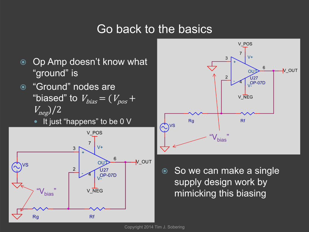
Go back to the basics
Op Amp doesn’t know what “ground” is
“Ground” nodes are “biased” to Vbias Vpos Vneg /2 It just “happens” to be 0 V
So we can make a single supply design work by mimicking this biasing
Copyright 2014 Tim J. Sobering
U27OP-07D
+3
-2
V+7
V-4
OUT6
V_POS
VS
V_OUT
RfRg
V_NEG
“Vbias”
“Vbias”

Single Supply Alternatives
Replace “ground” with VREF Make sure VREF is a low-
impedance source
Copyright 2014 Tim J. Sobering
U30
+3
-2
V+7
V-4
OUT6
V_REF
V_POS
VS4
V_OUT
RfRg
V_REF
U31OP-07D
+3
-2
V+7
V-4
OUT6
V_POS
V_POS
V_REF
R7
R8
Low-impedance reference

When in doubt, do the math!
Replace “ground” with VREF
1
If
Output swings relative to VREF
Copyright 2014 Tim J. Sobering
V_REF2
U32
+3
-2
V+7
V-4
OUT6
V_POS
VS5
V_OUT
Rg Rf
V_REF1

Key points for Single-Supply Design
Don’t inadvertently amplify your DC bias Extra biasing resistors can add noise
Use filtering caps if not in signal path
AC coupling works when biased correctly and DC response isn’t needed
Make sure your reference has a low source impedance Source impedance can change circuit gain
Watch out for CMR violations
Copyright 2014 Tim J. Sobering

Copyright 2014 Tim J. Sobering
Questions?