non-silicon solid state detectors harris kagan
TRANSCRIPT
Non-Silicon Solid State Detectors
Harris KaganOhio State University
42nd INFN Eloisatron WorkshopSep 29, 2003 - Erice, Italy
Outline of the Talk
• Introduction
• Status of Diamond Research
• Status of SiC Research
• Radiation Monitoring - a new application
• The Future
• Summary
42nd INFN Eloisatron Workshop
Sep 29, 2003 - Erice, Italy
Non-Silicon Solid State Detectors (page 1) Harris Kagan
Ohio State University
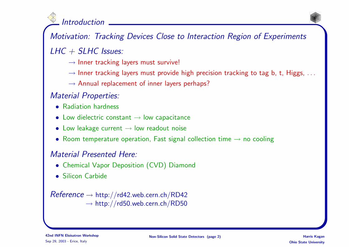
Introduction
Motivation: Tracking Devices Close to Interaction Region of Experiments
LHC + SLHC Issues:→ Inner tracking layers must survive!
→ Inner tracking layers must provide high precision tracking to tag b, t, Higgs, . . .
→ Annual replacement of inner layers perhaps?
Material Properties:• Radiation hardness
• Low dielectric constant → low capacitance
• Low leakage current → low readout noise
• Room temperature operation, Fast signal collection time → no cooling
Material Presented Here:• Chemical Vapor Deposition (CVD) Diamond
• Silicon Carbide
Reference → http://rd42.web.cern.ch/RD42→ http://rd50.web.cern.ch/RD50
42nd INFN Eloisatron Workshop
Sep 29, 2003 - Erice, Italy
Non-Silicon Solid State Detectors (page 2) Harris Kagan
Ohio State University
Introduction
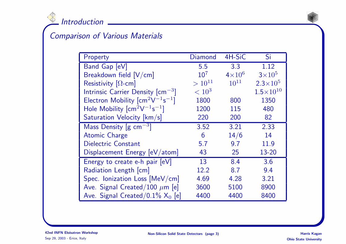
Comparison of Various Materials
Property Diamond 4H-SiC Si
Band Gap [eV] 5.5 3.3 1.12Breakdown field [V/cm] 107 4×10⁶ 3×10⁵
Resistivity [Ω-cm] > 1011 1011 2.3×10⁵
Intrinsic Carrier Density [cm−3] < 103 1.5×10¹⁰
Electron Mobility [cm2V−1s−1] 1800 800 1350Hole Mobility [cm2V−1s−1] 1200 115 480Saturation Velocity [km/s] 220 200 82
Mass Density [g cm−3] 3.52 3.21 2.33Atomic Charge 6 14/6 14Dielectric Constant 5.7 9.7 11.9Displacement Energy [eV/atom] 43 25 13-20
Energy to create e-h pair [eV] 13 8.4 3.6Radiation Length [cm] 12.2 8.7 9.4Spec. Ionization Loss [MeV/cm] 4.69 4.28 3.21Ave. Signal Created/100 µm [e] 3600 5100 8900Ave. Signal Created/0.1% X0 [e] 4400 4400 8400
42nd INFN Eloisatron Workshop
Sep 29, 2003 - Erice, Italy
Non-Silicon Solid State Detectors (page 3) Harris Kagan
Ohio State University

Diamond
Characterization of Diamond:
Signal formation
e-h Creation
Charged Particle
Electrodes
Diamond
Vbias
Amplifier
• Q=dtQ0 where d = collection distance = distance e-h pair move apart
• d=(µeτe + µhτh)E
• d=µEτ
with µ = µe + µh
and τ = µeτe+µhτh
µe+µh
42nd INFN Eloisatron Workshop
Sep 29, 2003 - Erice, Italy
Non-Silicon Solid State Detectors (page 4) Harris Kagan
Ohio State University
Diamond
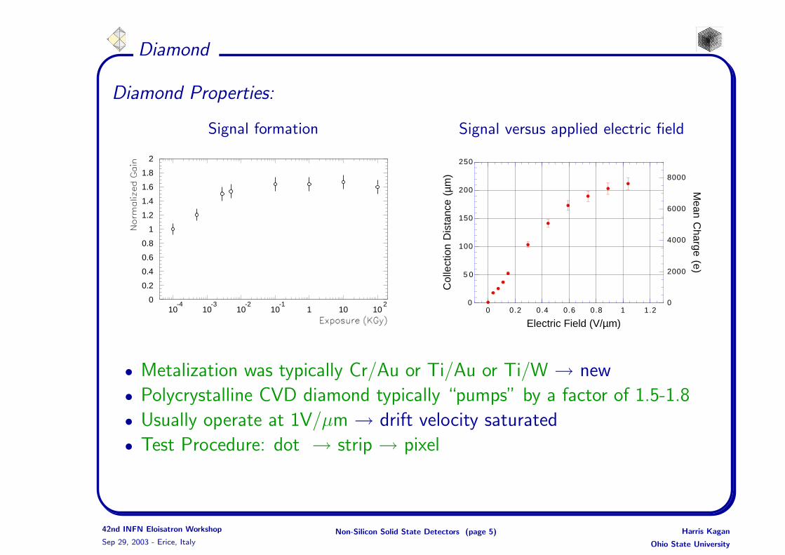
Diamond Properties:
Signal formation
0
0.2
0.4
0.6
0.8
1
1.2
1.4
1.6
1.8
2
10-4
10-3
10-2
10-1
1 10 102
Signal versus applied electric field
0
5 0
100
150
200
250
0 0 .2 0 .4 0 .6 0 .8 1 1 .20
2000
4000
6000
8000
Col
lect
ion
Dis
tanc
e ( µ
m)
Electric Field (V/µm)
Mean C
harge (e)
• Metalization was typically Cr/Au or Ti/Au or Ti/W → new
• Polycrystalline CVD diamond typically “pumps” by a factor of 1.5-1.8
• Usually operate at 1V/µm → drift velocity saturated
• Test Procedure: dot → strip → pixel
42nd INFN Eloisatron Workshop
Sep 29, 2003 - Erice, Italy
Non-Silicon Solid State Detectors (page 5) Harris Kagan
Ohio State University

Diamond
Growth side of a recent polycrystalline CVD (pCVD) diamond.
(Courtesy of Element Six)
42nd INFN Eloisatron Workshop
Sep 29, 2003 - Erice, Italy
Non-Silicon Solid State Detectors (page 6) Harris Kagan
Ohio State University
Diamond
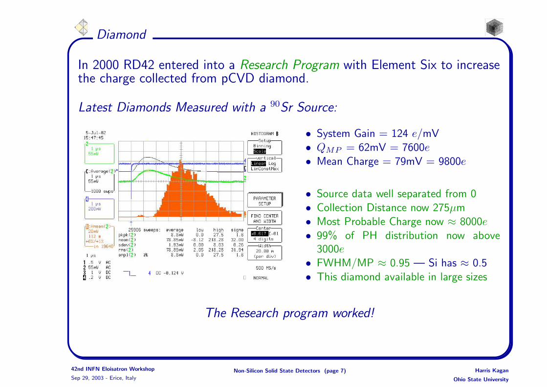
In 2000 RD42 entered into a Research Program with Element Six to increasethe charge collected from pCVD diamond.
Latest Diamonds Measured with a 90Sr Source:
• System Gain = 124 e/mV• QMP = 62mV = 7600e• Mean Charge = 79mV = 9800e
• Source data well separated from 0• Collection Distance now 275µm• Most Probable Charge now ≈ 8000e• 99% of PH distribution now above3000e
• FWHM/MP ≈ 0.95 — Si has ≈ 0.5• This diamond available in large sizes
The Research program worked!
42nd INFN Eloisatron Workshop
Sep 29, 2003 - Erice, Italy
Non-Silicon Solid State Detectors (page 7) Harris Kagan
Ohio State University
Diamond
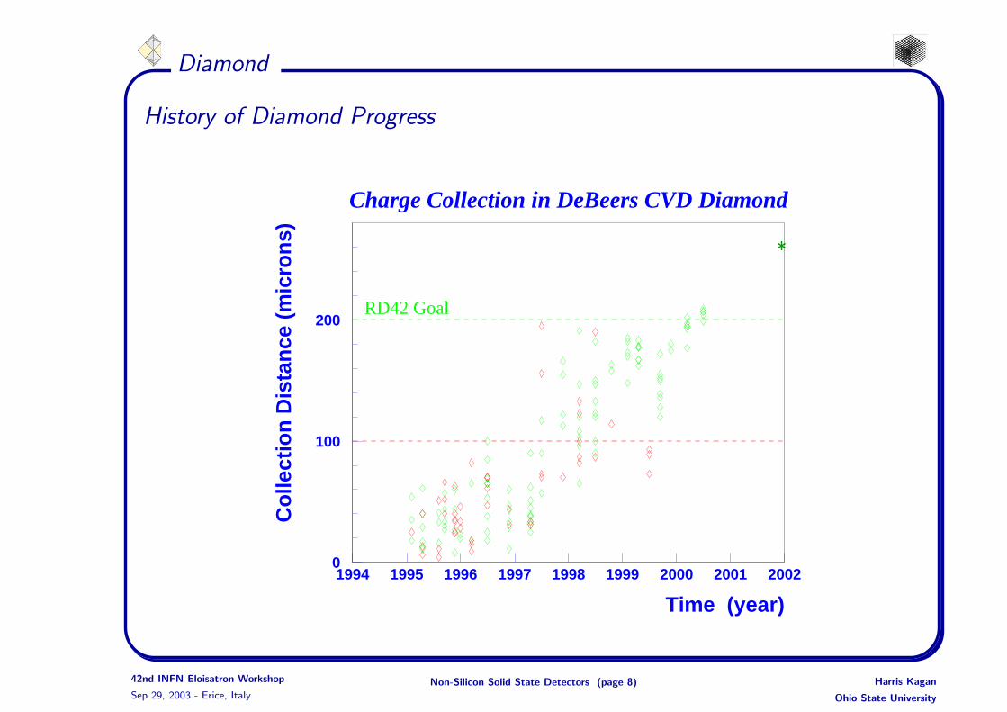
History of Diamond Progress
*
Charge Collection in DeBeers CVD Diamond
0
100
200
1994 1995 1996 1997 1998 1999 2000 2001 2002
RD42 Goal
Time (year)
Co
llect
ion
Dis
tan
ce (
mic
ron
s)
42nd INFN Eloisatron Workshop
Sep 29, 2003 - Erice, Italy
Non-Silicon Solid State Detectors (page 8) Harris Kagan
Ohio State University

Diamond
Recent pCVD diamond wafer ready for test:
42nd INFN Eloisatron Workshop
Sep 29, 2003 - Erice, Italy
Non-Silicon Solid State Detectors (page 9) Harris Kagan
Ohio State University
Diamond - Tracking Studies
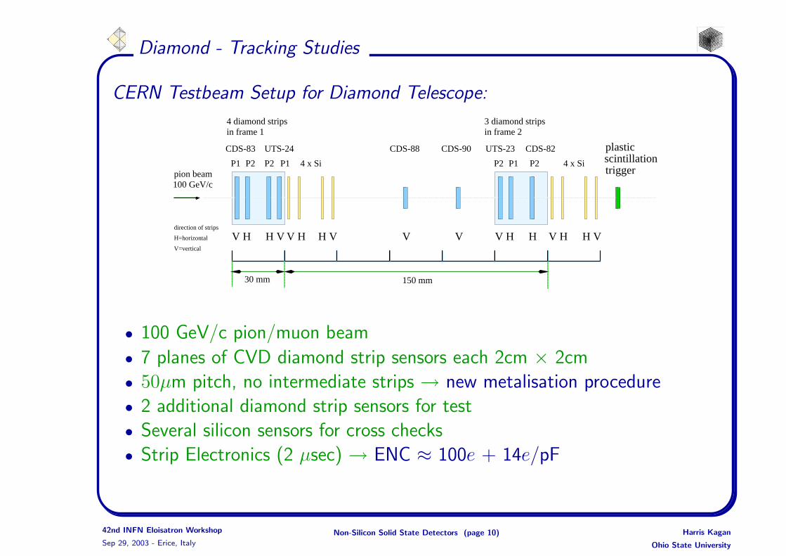
CERN Testbeam Setup for Diamond Telescope:
4 diamond stripsin frame 1 in frame 2
3 diamond strips
plastic
V V
30 mm
scintillationtrigger
150 mm
V HV H H V H V V H H H VV Hdirection of strips
H=horizontal
V=vertical
pion beam100 GeV/c
4 x Si4 x Si
CDS-88 CDS-90 UTS-23 CDS-82
P2P1P2
UTS-24CDS-83
P2P1 P2 P1
• 100 GeV/c pion/muon beam
• 7 planes of CVD diamond strip sensors each 2cm × 2cm
• 50µm pitch, no intermediate strips → new metalisation procedure
• 2 additional diamond strip sensors for test
• Several silicon sensors for cross checks
• Strip Electronics (2 µsec) → ENC ≈ 100e + 14e/pF
42nd INFN Eloisatron Workshop
Sep 29, 2003 - Erice, Italy
Non-Silicon Solid State Detectors (page 10) Harris Kagan
Ohio State University
Diamond - Tracking Studies
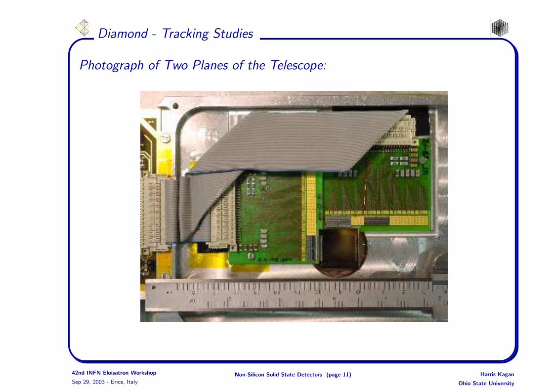
Photograph of Two Planes of the Telescope:
42nd INFN Eloisatron Workshop
Sep 29, 2003 - Erice, Italy
Non-Silicon Solid State Detectors (page 11) Harris Kagan
Ohio State University
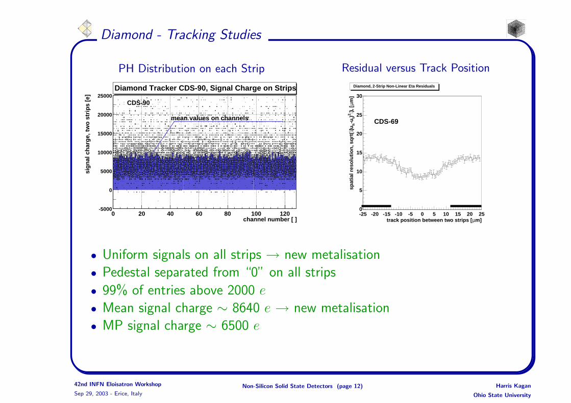
Diamond - Tracking Studies
PH Distribution on each Strip
channel number [ ]0 20 40 60 80 100 120
sig
nal
ch
arg
e, t
wo
str
ips
[e]
-5000
0
5000
10000
15000
20000
25000CDS-90
mean values on channels
Diamond Tracker CDS-90, Signal Charge on Strips
Residual versus Track Position
track position between two strips [ µ m] -25 -20 -15 -10 -5 0 5 10 15 20 25
spat
ial r
eso
luti
on
, sq
rt( ⟨
(u h -
u t ) 2 ⟩ )
, [ µ m
]
0
5
10
15
20
25
30
CDS-69
Diamond, 2-Strip Non-Linear Eta Residuals
• Uniform signals on all strips → new metalisation
• Pedestal separated from “0” on all strips
• 99% of entries above 2000 e
• Mean signal charge ∼ 8640 e → new metalisation
• MP signal charge ∼ 6500 e
42nd INFN Eloisatron Workshop
Sep 29, 2003 - Erice, Italy
Non-Silicon Solid State Detectors (page 12) Harris Kagan
Ohio State University

Diamond - Tracking Studies
Residuals
]2mµ
0.5
×
entr
ies
[per
120
0
5
10
15
20
25
30
35
40
m]µ, [track - Uhit(2cg)
residuals, U-100 -50 0 50 100
m]
µ [
trac
kU
-6000
-4000
-2000
0
2000
4000
6000
CDS-83-P1
Nent = 23513
Mean x = -0.965
Mean y = 1494
RMS x = 20.33
RMS y = 1867
215 10 2
1232 20399 1432
0 1 222
Integ = 2.04e+04
Diamond Detector PlaneCDS-83-P1
Residuals perpendicular to Strips
CDS-83-P1
Nent = 23513
Mean x = -0.965
Mean y = 1494
RMS x = 20.33
RMS y = 1867
215 10 2
1232 20399 1432
0 1 222
Integ = 2.04e+04]2
mµ 0
.5
×en
trie
s [p
er 1
20
0
5
10
15
20
25
30
35
40
]2mµ
0.5
×
entr
ies
[per
120
0
5
10
15
20
25
30
35
m]µ, [track - Uhit(2cg)
residuals, U-100 -50 0 50 100
m]
µ [
trac
kV
-6000
-4000
-2000
0
2000
4000
6000
CDS-83-P1
Nent = 23513
Mean x = -0.9702
Mean y = 190.9
RMS x = 20.31
RMS y = 1906
119 13 34
1291 20389 1420
37 8 202
Integ = 2.039e+04
Diamond Detector PlaneCDS-83-P1
Residuals along Strips
CDS-83-P1
Nent = 23513
Mean x = -0.9702
Mean y = 190.9
RMS x = 20.31
RMS y = 1906
119 13 34
1291 20389 1420
37 8 202
Integ = 2.039e+04
]2mµ
0.5
×
entr
ies
[per
120
0
5
10
15
20
25
30
35
42nd INFN Eloisatron Workshop
Sep 29, 2003 - Erice, Italy
Non-Silicon Solid State Detectors (page 13) Harris Kagan
Ohio State University

Diamond - Tracking Studies
Next advance → take advantage of charge sharing:
Use intermediate strips to force charge sharing.
42nd INFN Eloisatron Workshop
Sep 29, 2003 - Erice, Italy
Non-Silicon Solid State Detectors (page 14) Harris Kagan
Ohio State University
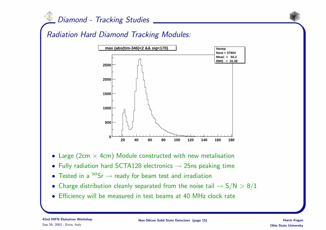
Diamond - Tracking Studies
Radiation Hard Diamond Tracking Modules:
20 40 60 80 100 120 140 160 1800
500
1000
1500
2000
2500
htempNent = 37904 Mean = 50.2RMS = 16.38
max abs(tim-346)<2 && sig<170 htempNent = 37904 Mean = 50.2RMS = 16.38
• Large (2cm × 4cm) Module constructed with new metalisation
• Fully radiation hard SCTA128 electronics → 25ns peaking time
• Tested in a 90Sr → ready for beam test and irradiation
• Charge distribution cleanly separated from the noise tail → S/N > 8/1
• Efficiency will be measured in test beams at 40 MHz clock rate
42nd INFN Eloisatron Workshop
Sep 29, 2003 - Erice, Italy
Non-Silicon Solid State Detectors (page 15) Harris Kagan
Ohio State University

Diamond Pixel Detectors
ATLAS FE/I Pixels (Al)
• Atlas pixel pitch 50µm × 400µm• Over Metalisation: Al• Lead-tin solder bumping at IZM in Berlin
CMS Pixels (Ti-W)
• CMS pixel pitch 125µm × 125µm• Metalization: Ti/W• Indium bumping at UC Davis
→ Bump bonding yield ≈ 100 % for both ATLAS and CMS devices
New radiation hard chips produced this year.
42nd INFN Eloisatron Workshop
Sep 29, 2003 - Erice, Italy
Non-Silicon Solid State Detectors (page 16) Harris Kagan
Ohio State University
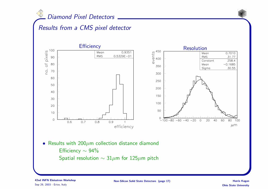
Diamond Pixel Detectors
Results from a CMS pixel detector
Efficiency Resolution
• Results with 200µm collection distance diamond
Efficiency ∼ 94%
Spatial resolution ∼ 31µm for 125µm pitch
42nd INFN Eloisatron Workshop
Sep 29, 2003 - Erice, Italy
Non-Silicon Solid State Detectors (page 17) Harris Kagan
Ohio State University

Diamond Pixel Detectors
Results from a CMS pixel detector
Efficiency vs Pixel
• Inefficient pixels due to bump bonding and/or electronics - shown in pulser tests
• Excellent correlation between beam telescope and pixel tracker data!
42nd INFN Eloisatron Workshop
Sep 29, 2003 - Erice, Italy
Non-Silicon Solid State Detectors (page 18) Harris Kagan
Ohio State University
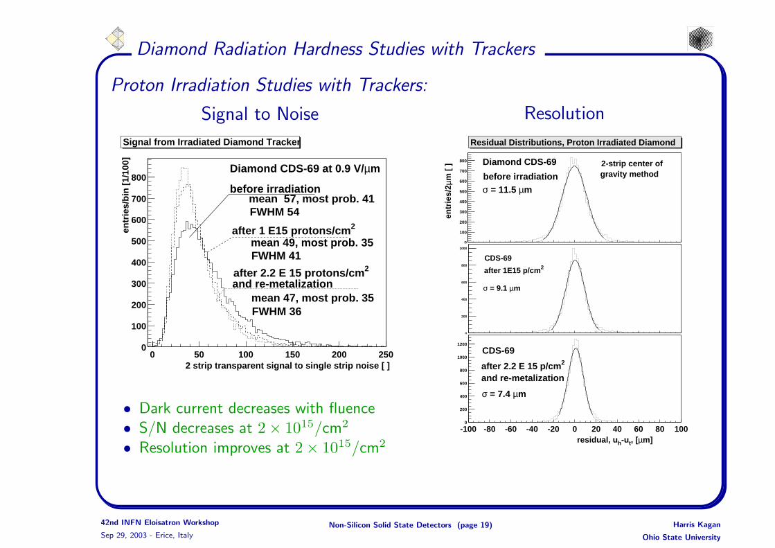
Diamond Radiation Hardness Studies with Trackers
Proton Irradiation Studies with Trackers:
Signal to Noise
2 strip transparent signal to single strip noise [ ]0 50 100 150 200 250
entr
ies/
bin
[1/
100]
0
100
200
300
400
500
600
700
800before irradiation
mean 57, most prob. 41FWHM 54
after 1 E15 protons/cm2
mean 49, most prob. 35FWHM 41
Diamond CDS-69 at 0.9 V/µm
after 2.2 E 15 protons/cm2
and re-metalizationmean 47, most prob. 35FWHM 36
Signal from Irradiated Diamond Tracker
• Dark current decreases with fluence• S/N decreases at 2× 10¹⁵/cm2
• Resolution improves at 2× 10¹⁵/cm2
Resolution
entr
ies/
2µm
[ ]
0
100
200
300
400
500
600
700
800
Residual Distributions, Proton Irradiated Diamond
Diamond CDS-69
before irradiationσ = 11.5 µm
2-strip center ofgravity method
0
200
400
600
800
1000
CDS-69
after 1E15 p/cm2
σ = 9.1 µm
residual, uh-ut, [µm]-100 -80 -60 -40 -20 0 20 40 60 80 100
0
200
400
600
800
1000
1200
CDS-69
after 2.2 E 15 p/cm2
and re-metalization
σ = 7.4 µm
42nd INFN Eloisatron Workshop
Sep 29, 2003 - Erice, Italy
Non-Silicon Solid State Detectors (page 19) Harris Kagan
Ohio State University
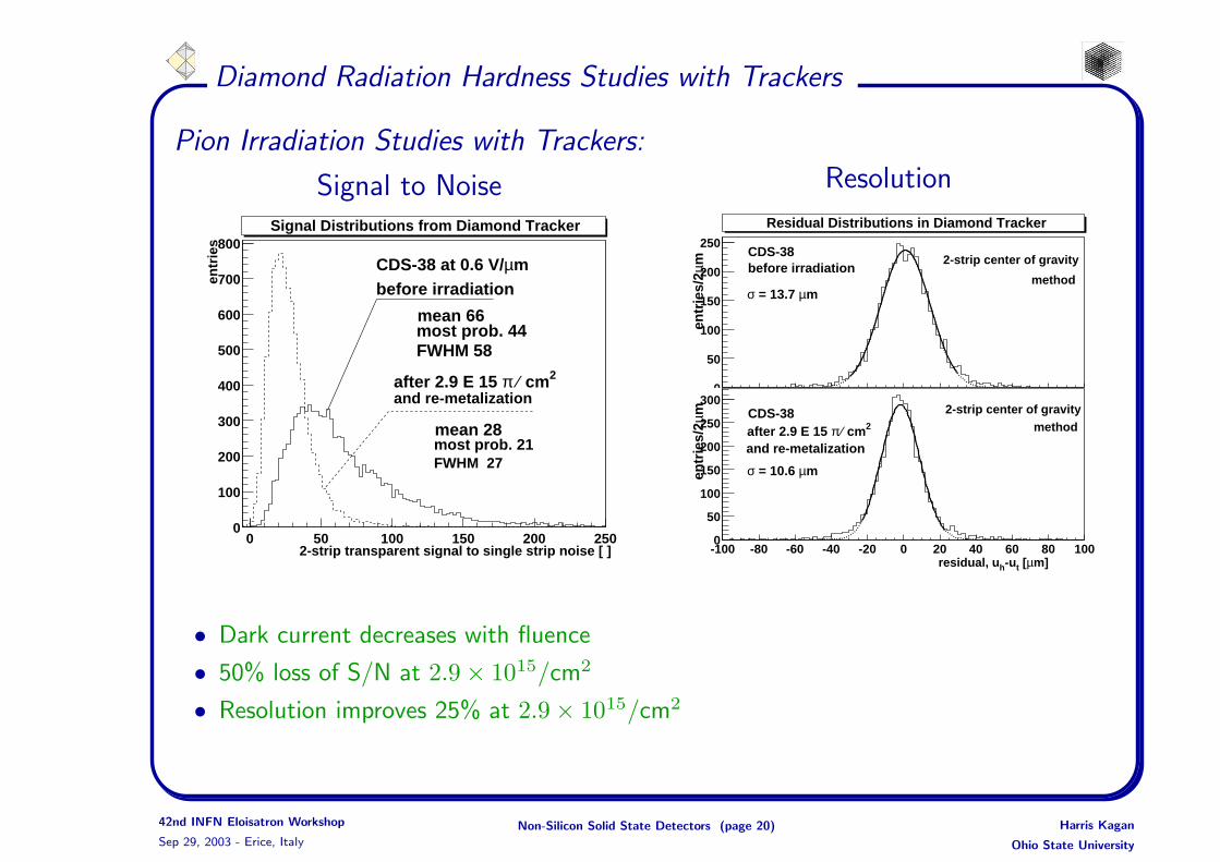
Diamond Radiation Hardness Studies with Trackers
Pion Irradiation Studies with Trackers:
Signal to Noise
2-strip transparent signal to single strip noise [ ]0 50 100 150 200 250
entr
ies
0
100
200
300
400
500
600
700
800
CDS-38 at 0.6 V/µmbefore irradiation
mean 66most prob. 44FWHM 58
cm2⁄after 2.9 E 15 π
mean 28
and re-metalization
most prob. 21FWHM 27
Signal Distributions from Diamond Tracker
Resolution
entr
ies/
2µm
0
50
100
150
200
250CDS-38before irradiation
σ = 13.7 µm
2-strip center of gravity
method
Residual Distributions in Diamond Tracker
residual, uh-ut [µm]-100 -80 -60 -40 -20 0 20 40 60 80 100
entr
ies/
2µm
0
50
100
150
200
250
300CDS-38
cm2⁄after 2.9 E 15 π
σ = 10.6 µm
and re-metalization
2-strip center of gravitymethod
• Dark current decreases with fluence
• 50% loss of S/N at 2.9× 10¹⁵/cm2
• Resolution improves 25% at 2.9× 10¹⁵/cm2
42nd INFN Eloisatron Workshop
Sep 29, 2003 - Erice, Italy
Non-Silicon Solid State Detectors (page 20) Harris Kagan
Ohio State University
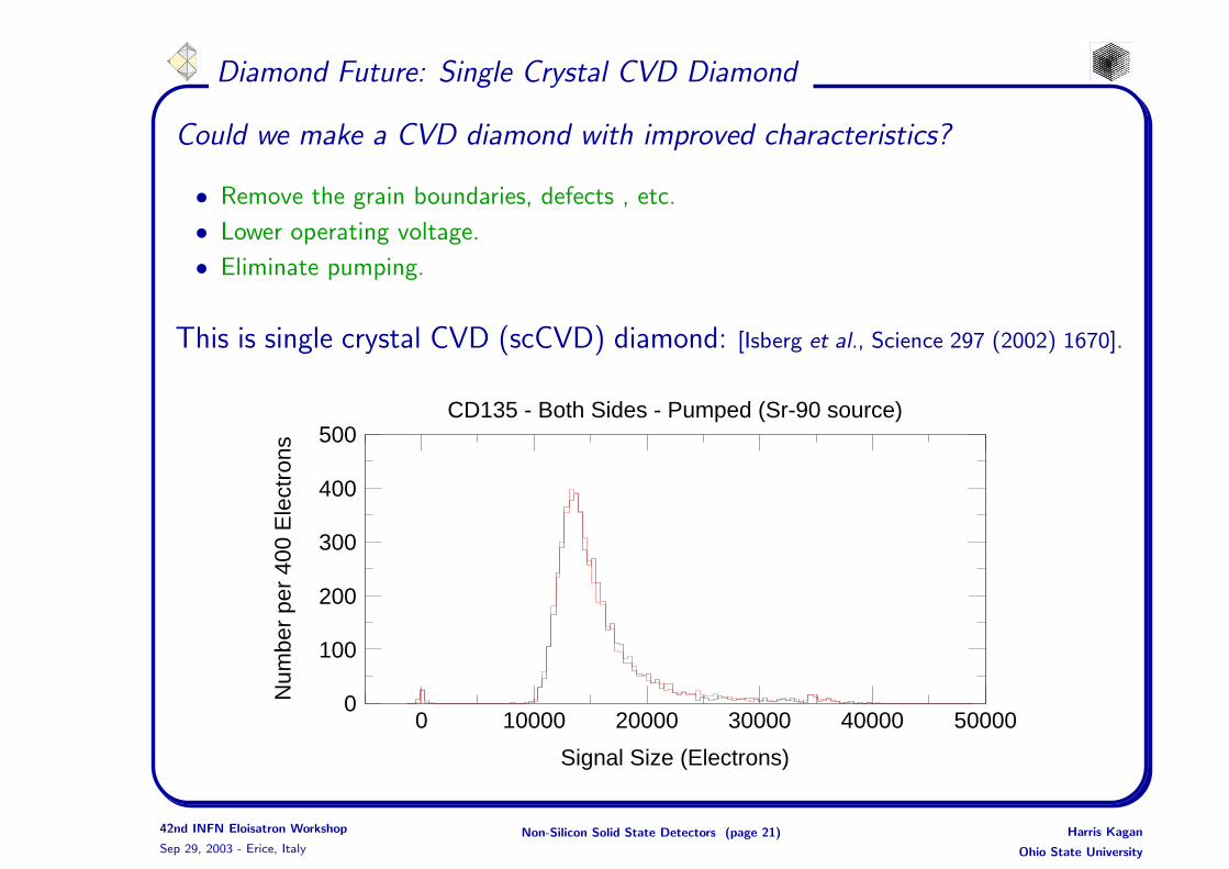
Diamond Future: Single Crystal CVD Diamond
Could we make a CVD diamond with improved characteristics?
• Remove the grain boundaries, defects , etc.
• Lower operating voltage.
• Eliminate pumping.
This is single crystal CVD (scCVD) diamond: [Isberg et al., Science 297 (2002) 1670].
CD135 - Both Sides - Pumped (Sr-90 source)
0 10000 20000 30000 40000 50000
Signal Size (Electrons)
0
100
200
300
400
500
Num
ber
per
400
Ele
ctro
ns
42nd INFN Eloisatron Workshop
Sep 29, 2003 - Erice, Italy
Non-Silicon Solid State Detectors (page 21) Harris Kagan
Ohio State University
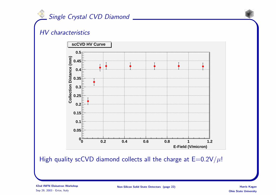
Single Crystal CVD Diamond
HV characteristics
E-Field (V/micron)0 0.2 0.4 0.6 0.8 1 1.2
Co
llect
ion
Dis
tan
ce (
mm
)
0
0.05
0.1
0.15
0.2
0.25
0.3
0.35
0.4
0.45
0.5
scCVD HV Curve
High quality scCVD diamond collects all the charge at E=0.2V/µ!
42nd INFN Eloisatron Workshop
Sep 29, 2003 - Erice, Italy
Non-Silicon Solid State Detectors (page 22) Harris Kagan
Ohio State University
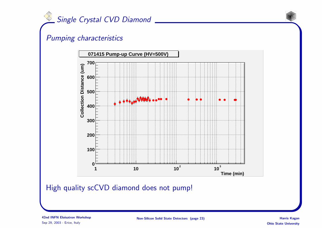
Single Crystal CVD Diamond
Pumping characteristics
Time (min)1 10 10
210
3
Co
llect
ion
Dis
tan
ce (
um
)
0
100
200
300
400
500
600
700
071415 Pump-up Curve (HV=500V)
High quality scCVD diamond does not pump!
42nd INFN Eloisatron Workshop
Sep 29, 2003 - Erice, Italy
Non-Silicon Solid State Detectors (page 23) Harris Kagan
Ohio State University

Silicon Carbide
Structures in 4H-SiC:
The properties of silicon carbide are in some sense the geometric meanbetween silicon and diamond. As a result one hopes to take advantage of thestrengths of both. Two types of SiC structures have been studied:
In SemiInsulating material the charge collection depends on native defects;Epitaxial material has low native defects but only exists in thin layers.
42nd INFN Eloisatron Workshop
Sep 29, 2003 - Erice, Italy
Non-Silicon Solid State Detectors (page 24) Harris Kagan
Ohio State University
Silicon Carbide
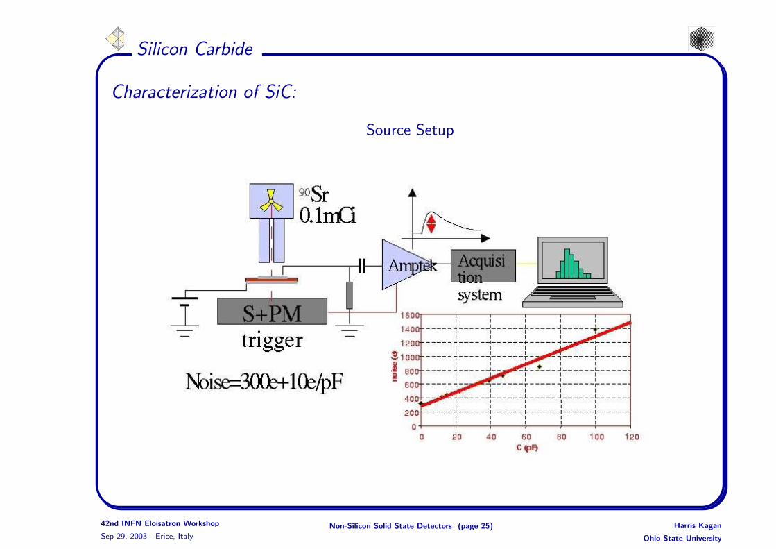
Characterization of SiC:
Source Setup
42nd INFN Eloisatron Workshop
Sep 29, 2003 - Erice, Italy
Non-Silicon Solid State Detectors (page 25) Harris Kagan
Ohio State University
Silicon Carbide
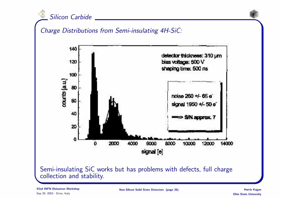
Charge Distributions from Semi-insulating 4H-SiC:
Semi-insulating SiC works but has problems with defects, full chargecollection and stability.
42nd INFN Eloisatron Workshop
Sep 29, 2003 - Erice, Italy
Non-Silicon Solid State Detectors (page 26) Harris Kagan
Ohio State University
Silicon Carbide
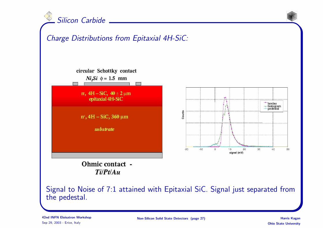
Charge Distributions from Epitaxial 4H-SiC:
Signal to Noise of 7:1 attained with Epitaxial SiC. Signal just separated fromthe pedestal.
42nd INFN Eloisatron Workshop
Sep 29, 2003 - Erice, Italy
Non-Silicon Solid State Detectors (page 27) Harris Kagan
Ohio State University
Silicon Carbide
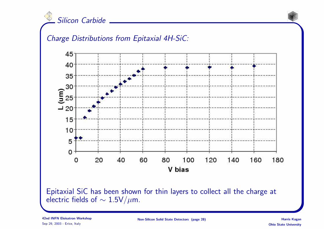
Charge Distributions from Epitaxial 4H-SiC:
Epitaxial SiC has been shown for thin layers to collect all the charge atelectric fields of ∼ 1.5V/µm.
42nd INFN Eloisatron Workshop
Sep 29, 2003 - Erice, Italy
Non-Silicon Solid State Detectors (page 28) Harris Kagan
Ohio State University
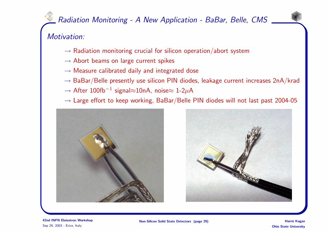
Radiation Monitoring - A New Application - BaBar, Belle, CMS
Motivation:
→ Radiation monitoring crucial for silicon operation/abort system
→ Abort beams on large current spikes
→ Measure calibrated daily and integrated dose
→ BaBar/Belle presently use silicon PIN diodes, leakage current increases 2nA/krad
→ After 100fb−1 signal≈10nA, noise≈ 1-2µA
→ Large effort to keep working, BaBar/Belle PIN diodes will not last past 2004-05
42nd INFN Eloisatron Workshop
Sep 29, 2003 - Erice, Italy
Non-Silicon Solid State Detectors (page 29) Harris Kagan
Ohio State University
Radiation Monitoring
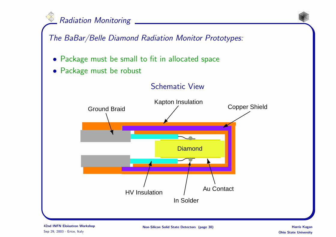
The BaBar/Belle Diamond Radiation Monitor Prototypes:
• Package must be small to fit in allocated space
• Package must be robust
Schematic View
Diamond
Au Contact
In SolderHV Insulation
Ground BraidKapton Insulation
Copper Shield
42nd INFN Eloisatron Workshop
Sep 29, 2003 - Erice, Italy
Non-Silicon Solid State Detectors (page 30) Harris Kagan
Ohio State University

Radiation Monitoring
The BaBar/Belle Diamond Radiation Monitor Prototypes:
Photo of Belle Prototype Device Photo of Packaged Belle Prototype
42nd INFN Eloisatron Workshop
Sep 29, 2003 - Erice, Italy
Non-Silicon Solid State Detectors (page 31) Harris Kagan
Ohio State University
Radiation Monitoring
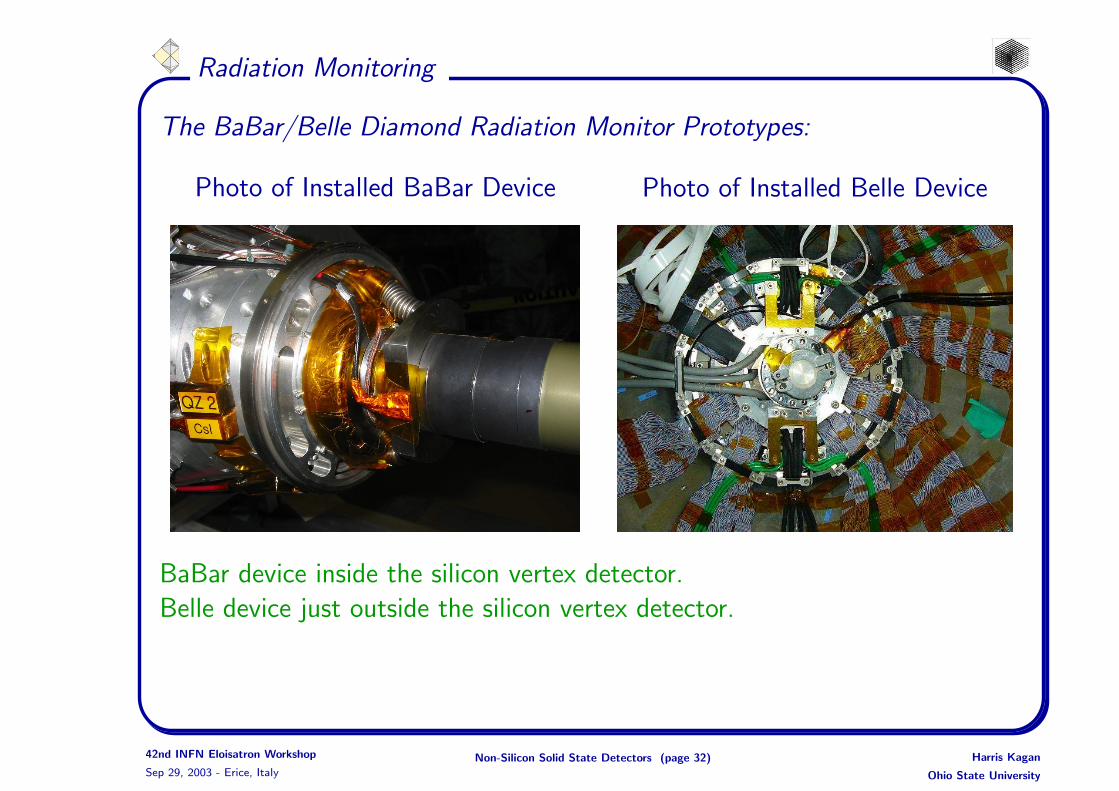
The BaBar/Belle Diamond Radiation Monitor Prototypes:
Photo of Installed BaBar Device Photo of Installed Belle Device
BaBar device inside the silicon vertex detector.
Belle device just outside the silicon vertex detector.
42nd INFN Eloisatron Workshop
Sep 29, 2003 - Erice, Italy
Non-Silicon Solid State Detectors (page 32) Harris Kagan
Ohio State University
Radiation Monitoring
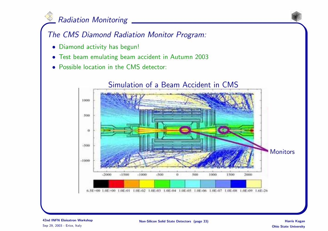
The CMS Diamond Radiation Monitor Program:
• Diamond activity has begun!
• Test beam emulating beam accident in Autumn 2003
• Possible location in the CMS detector:
Monitors
Simulation of a Beam Accident in CMS
42nd INFN Eloisatron Workshop
Sep 29, 2003 - Erice, Italy
Non-Silicon Solid State Detectors (page 33) Harris Kagan
Ohio State University
Radiation Monitoring
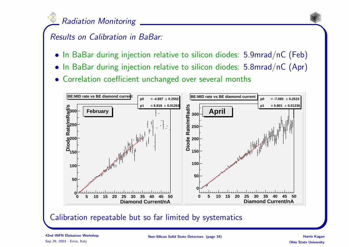
Results on Calibration in BaBar:
• In BaBar during injection relative to silicon diodes: 5.9mrad/nC (Feb)
• In BaBar during injection relative to silicon diodes: 5.8mrad/nC (Apr)
• Correlation coefficient unchanged over several months
Diamond Current/nA0 5 10 15 20 25 30 35 40 45 50
Dio
de
Rat
e/m
Rad
/s
0
50
100
150
200
250
300
0.2552 ±p0 = -4.897
0.01263 ±p1 = 5.916
February
BE:MID rate vs BE diamond current 0.2552 ±p0 = -4.897
0.01263 ±p1 = 5.916
Diamond Current/nA0 5 10 15 20 25 30 35 40 45 50
Dio
de
Rat
e/m
Rad
/s0
50
100
150
200
250
300
0.2533 ±p0 = -7.085
0.01236 ±p1 = 5.801
April
BE:MID rate vs BE diamond current 0.2533 ±p0 = -7.085
0.01236 ±p1 = 5.801
Calibration repeatable but so far limited by systematics
42nd INFN Eloisatron Workshop
Sep 29, 2003 - Erice, Italy
Non-Silicon Solid State Detectors (page 34) Harris Kagan
Ohio State University

Radiation Monitoring
Data Taking in BaBar:
0
5
10
15
20
25
0 2500 5000 7500 10000 12500 15000 17500 20000 225000
200
400
600
800
1000
1200
1400
1600
1800
20000 2500 5000 7500 10000 12500 15000 17500 20000 22500
BE diamond current
BE:MID diode signal current (Sig 11)
LER current
Time/seconds
Dia
mon
d/D
iode
cur
rent
/nA
Time/secondsH
ER
cur
rent
/mA
Fast Abort Soft Abort
System operating for 4 months in BaBar and works well!
42nd INFN Eloisatron Workshop
Sep 29, 2003 - Erice, Italy
Non-Silicon Solid State Detectors (page 35) Harris Kagan
Ohio State University
Radiation Monitoring
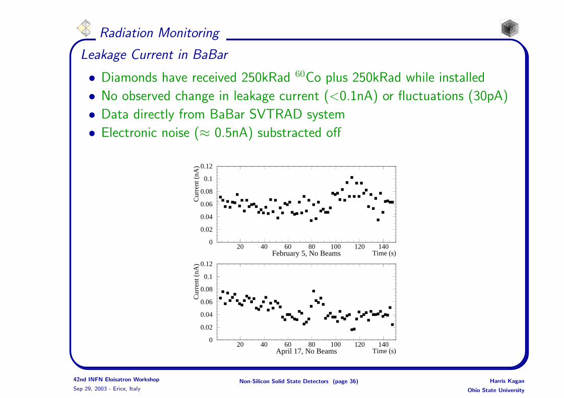
Leakage Current in BaBar
• Diamonds have received 250kRad 60Co plus 250kRad while installed
• No observed change in leakage current (<0.1nA) or fluctuations (30pA)
• Data directly from BaBar SVTRAD system
• Electronic noise (≈ 0.5nA) substracted off
0
0.02
0.04
0.06
0.08
0.1
0.12
20 40 60 80 100 120 140February 5, No Beams Time (s)
Cur
rent
(nA
)
April 17, No Beams Time (s)
Cur
rent
(nA
)
0
0.02
0.04
0.06
0.08
0.1
0.12
20 40 60 80 100 120 140
42nd INFN Eloisatron Workshop
Sep 29, 2003 - Erice, Italy
Non-Silicon Solid State Detectors (page 36) Harris Kagan
Ohio State University
Radiation Monitoring
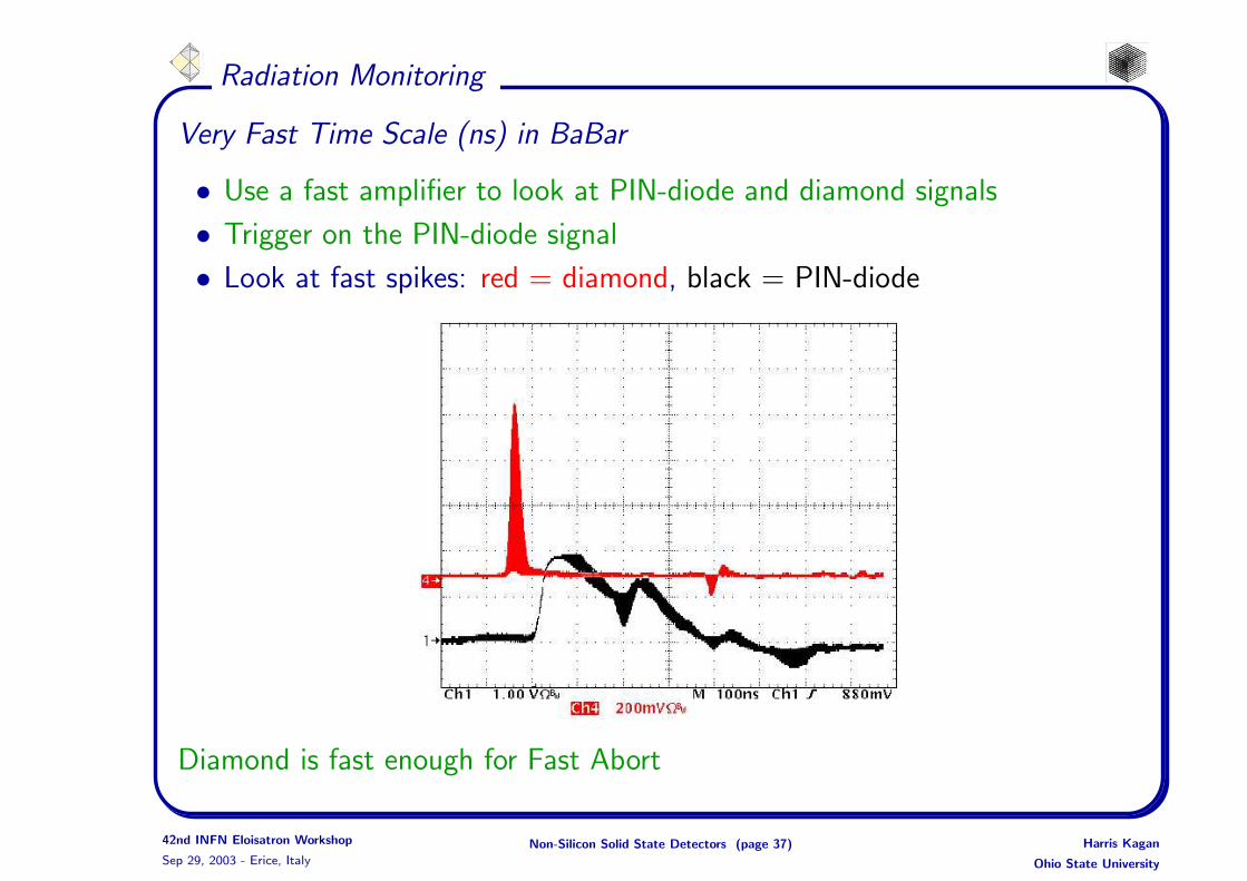
Very Fast Time Scale (ns) in BaBar
• Use a fast amplifier to look at PIN-diode and diamond signals
• Trigger on the PIN-diode signal
• Look at fast spikes: red = diamond, black = PIN-diode
Diamond is fast enough for Fast Abort
42nd INFN Eloisatron Workshop
Sep 29, 2003 - Erice, Italy
Non-Silicon Solid State Detectors (page 37) Harris Kagan
Ohio State University
Radiation Monitoring
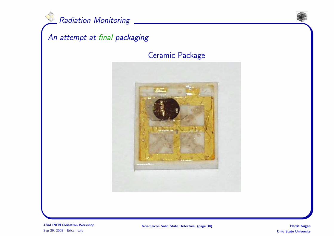
An attempt at final packaging
Ceramic Package
42nd INFN Eloisatron Workshop
Sep 29, 2003 - Erice, Italy
Non-Silicon Solid State Detectors (page 38) Harris Kagan
Ohio State University

The Future
• Diamond and silicon carbide have very promising futures
• Diamond work is being pursued by RD42 pCVD → scCVD
• SiC work is being pursued by RD50 epi layers → 100µm
• Present pCVD diamonds should surpass the performance of present silicon at around1015p/cm2
• Semi-insulating SiC will require lots of engineering
42nd INFN Eloisatron Workshop
Sep 29, 2003 - Erice, Italy
Non-Silicon Solid State Detectors (page 39) Harris Kagan
Ohio State University
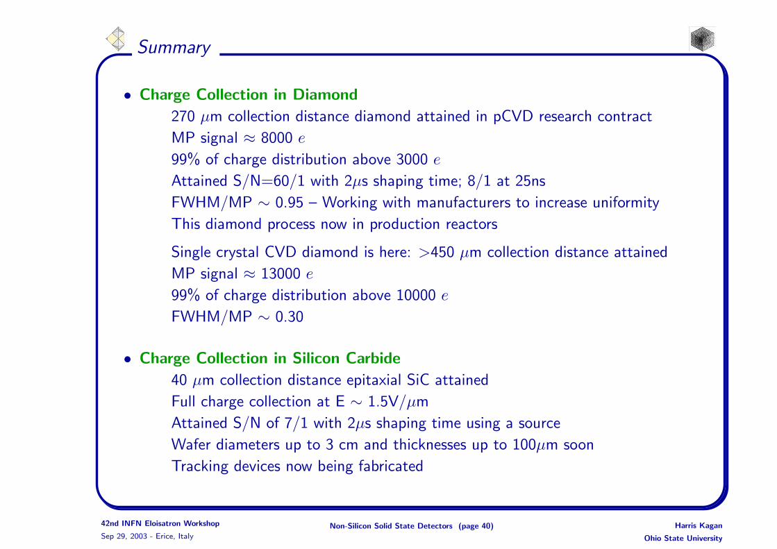
Summary
• Charge Collection in Diamond
270 µm collection distance diamond attained in pCVD research contract
MP signal ≈ 8000 e
99% of charge distribution above 3000 e
Attained S/N=60/1 with 2µs shaping time; 8/1 at 25ns
FWHM/MP ∼ 0.95 – Working with manufacturers to increase uniformity
This diamond process now in production reactors
Single crystal CVD diamond is here: >450 µm collection distance attained
MP signal ≈ 13000 e
99% of charge distribution above 10000 e
FWHM/MP ∼ 0.30
• Charge Collection in Silicon Carbide
40 µm collection distance epitaxial SiC attained
Full charge collection at E ∼ 1.5V/µm
Attained S/N of 7/1 with 2µs shaping time using a source
Wafer diameters up to 3 cm and thicknesses up to 100µm soon
Tracking devices now being fabricated
42nd INFN Eloisatron Workshop
Sep 29, 2003 - Erice, Italy
Non-Silicon Solid State Detectors (page 40) Harris Kagan
Ohio State University

Summary
• Radiation Hardness of Large Bandgap SemiConductors
Using trackers allows a correlation between S/N and Resolution
Dark current decreases with fluence
Some loss of S/N with fluence
Resolution improves with fluence
Tests must be repeated with more trackers and latest pCVD and scCVD
diamonds and Epitaxial 4H-SiC
• Radiation Monitoring
Successfully tested BaBar and Belle devices
CMS performing tests this summer
Radiation monitoring should lead to the development of the next levelradiation hard devices
42nd INFN Eloisatron Workshop
Sep 29, 2003 - Erice, Italy
Non-Silicon Solid State Detectors (page 41) Harris Kagan
Ohio State University

Future Plans for RD42
• Charge Collection
Continue research program to improve pCVD material:
collection distance → 300µm (Q = 10, 800e)
→ improved uniformity
→ identification of trapping centers
Begin research program on scCVD diamond
• Radiation Hardness of Diamond Trackers and Pixel Detectors
Continue tracker irradiations this year, add pixel irradiations
With Protons:
→ 5× 10¹⁵/cm2
With Pions:
→ 5× 10¹⁵/cm2
With Neutrons:
→ 5× 10¹⁵/cm2
• Beam Tests with Diamond Trackers and Pixel Detectors
→ trackers with intermediate strips, SCTA128 electronics
→ pixel detectors with ATLAS and CMS radhard electronics now available!
→ construct the first full ATLAS diamond pixel module
• Material Research
→ Florence, OSU, Paris, Rome
42nd INFN Eloisatron Workshop
Sep 29, 2003 - Erice, Italy
Non-Silicon Solid State Detectors (page 42) Harris Kagan
Ohio State University
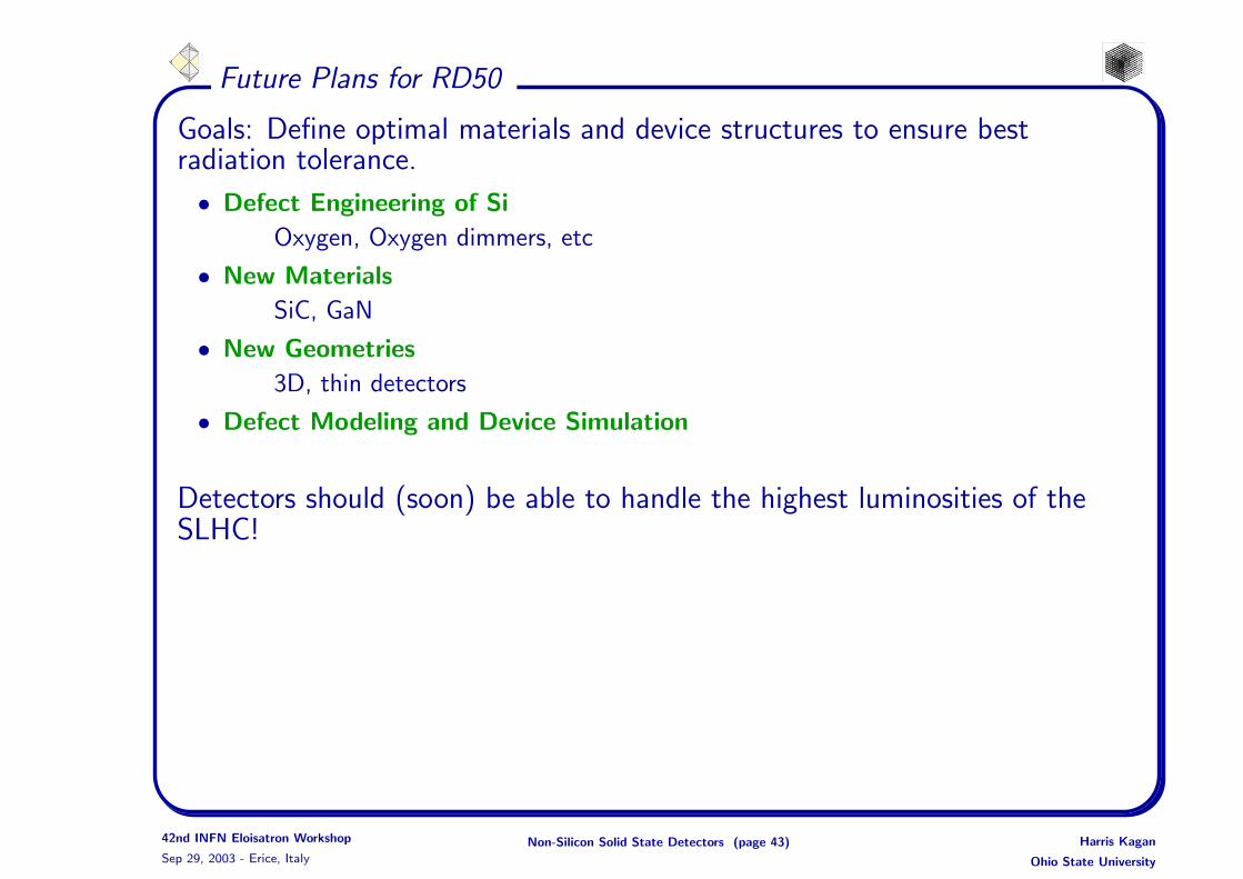
Future Plans for RD50
Goals: Define optimal materials and device structures to ensure bestradiation tolerance.
• Defect Engineering of Si
Oxygen, Oxygen dimmers, etc
• New Materials
SiC, GaN
• New Geometries
3D, thin detectors
• Defect Modeling and Device Simulation
Detectors should (soon) be able to handle the highest luminosities of theSLHC!
42nd INFN Eloisatron Workshop
Sep 29, 2003 - Erice, Italy
Non-Silicon Solid State Detectors (page 43) Harris Kagan
Ohio State University