non-synchronous pfet step-down controller
TRANSCRIPT

XXRRPP66112244 NNoonn--SSyynncchhrroonnoouuss PPFFEETT SStteepp--DDoowwnn CCoonnttrroolllleerr
May 2018 Rev. 1.1.1
1/12 Rev. 1.1.1
GENERAL DESCRIPTION The XRP6124 is a non synchronous step down (buck) controller for up to 5Amps point of loads. A wide 3V to 30V input voltage range allows for single supply operations from industry standard 3.3V, 5V, 12V and 24V power rails.
With a proprietary Constant On-Time (COT) control scheme, the XRP6124 provides extremely fast line and load transient response while the operating frequency remains nearly constant. It requires no loop compensation hence simplifying circuit implementation and reducing overall component count. The XRP76124 also implements an emulated ESR circuitry allowing usage of ceramic output capacitors and insuring stable operations without the use of extra external components.
Built-in soft start prevents high inrush currents while under voltage lock-out and output short protections insure safe operations under abnormal operating conditions.
The XRP6124 is available in a RoHS compliant, green/halogen free space-saving 5-pin SOT23 package.
APPLICATIONS • Point of Load Conversions
• Audio-Video Equipment
• Industrial and Medical Equipment
• Distributed Power Architecture
FEATURES • 5A Point-of-Load Capable − Down to 1.2V Output Voltage Conversion
• Wide Input Voltage Range − 3V to 18V: XRP6124 − 4.5V to 30V: XRP6124HV
• Constant On-Time Operations − Constant Frequency Operations − No External Compensation − Supports Ceramic Output Capacitors
• Built-in 2ms Soft Start
• Short Circuit Protection
• <1µA shutdown current
• RoHS Compliant, Green/Halogen Free 5-pin SOT23 Package
TYPICAL APPLICATION DIAGRAM
Figure 1: XRP6124 Application Diagram
XXRRPP66112244 NNoonn--SSyynncchhrroonnoouuss PPFFEETT SStteepp--DDoowwnn CCoonnttrroolllleerr
2/12 Rev. 1.1.1
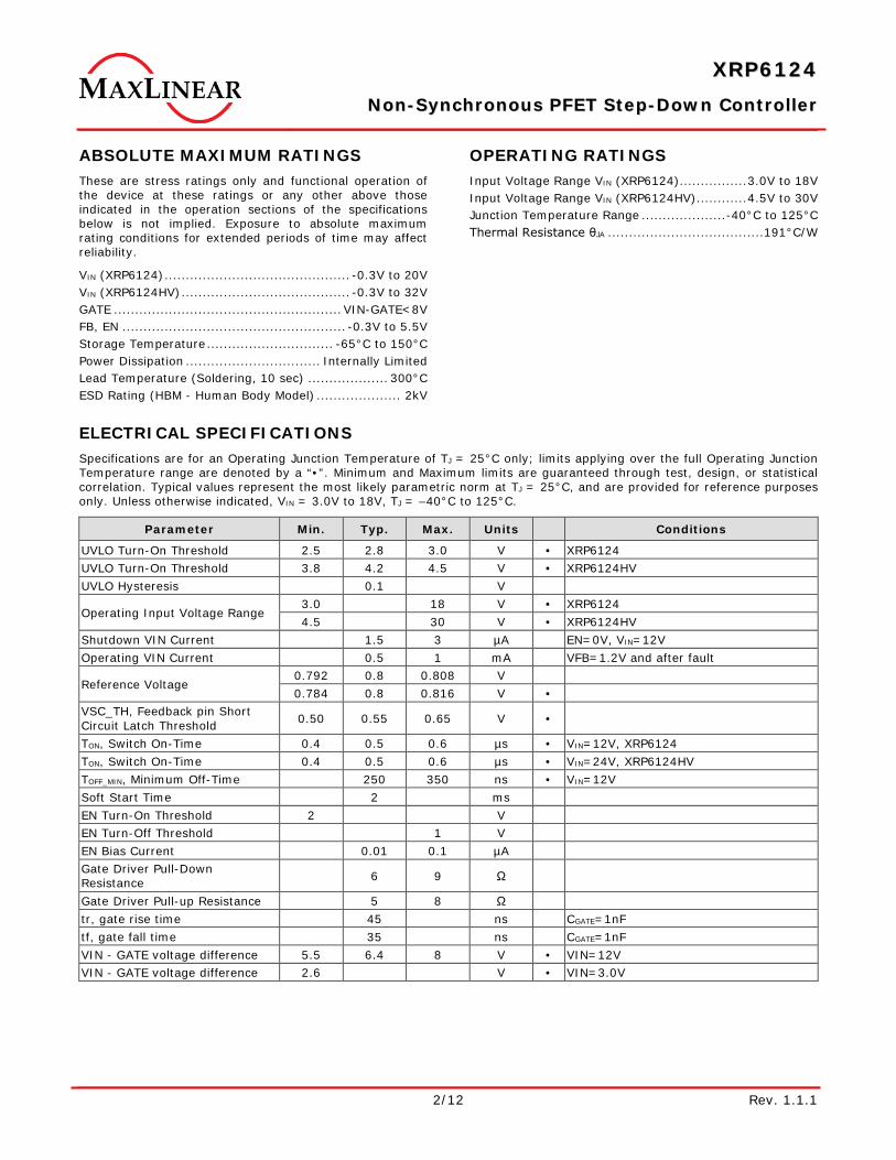
ABSOLUTE MAXIMUM RATINGS These are stress ratings only and functional operation of the device at these ratings or any other above those indicated in the operation sections of the specifications below is not implied. Exposure to absolute maximum rating conditions for extended periods of time may affect reliability.
VIN (XRP6124) ............................................ -0.3V to 20V VIN (XRP6124HV) ........................................ -0.3V to 32V GATE ...................................................... VIN-GATE<8V FB, EN ..................................................... -0.3V to 5.5V Storage Temperature .............................. -65°C to 150°C Power Dissipation ................................ Internally Limited Lead Temperature (Soldering, 10 sec) ................... 300°C ESD Rating (HBM - Human Body Model) .................... 2kV
OPERATING RATINGS Input Voltage Range VIN (XRP6124) ................ 3.0V to 18V Input Voltage Range VIN (XRP6124HV) ............ 4.5V to 30V Junction Temperature Range .................... -40°C to 125°C Thermal Resistance θJA .....................................191°C/W
ELECTRICAL SPECIFICATIONS Specifications are for an Operating Junction Temperature of TJ = 25°C only; limits applying over the full Operating Junction Temperature range are denoted by a “•”. Minimum and Maximum limits are guaranteed through test, design, or statistical correlation. Typical values represent the most likely parametric norm at TJ = 25°C, and are provided for reference purposes only. Unless otherwise indicated, VIN = 3.0V to 18V, TJ = –40°C to 125°C.
Parameter Min. Typ. Max. Units Conditions
UVLO Turn-On Threshold 2.5 2.8 3.0 V • XRP6124 UVLO Turn-On Threshold 3.8 4.2 4.5 V • XRP6124HV UVLO Hysteresis 0.1 V
Operating Input Voltage Range 3.0 18 V • XRP6124 4.5 30 V • XRP6124HV
Shutdown VIN Current 1.5 3 µA EN=0V, VIN=12V Operating VIN Current 0.5 1 mA VFB=1.2V and after fault
Reference Voltage 0.792 0.8 0.808 V 0.784 0.8 0.816 V •
VSC_TH, Feedback pin Short Circuit Latch Threshold 0.50 0.55 0.65 V •
TON, Switch On-Time 0.4 0.5 0.6 µs • VIN=12V, XRP6124 TON, Switch On-Time 0.4 0.5 0.6 µs • VIN=24V, XRP6124HV TOFF_MIN, Minimum Off-Time 250 350 ns • VIN=12V Soft Start Time 2 ms EN Turn-On Threshold 2 V EN Turn-Off Threshold 1 V EN Bias Current 0.01 0.1 µA Gate Driver Pull-Down Resistance 6 9 Ω
Gate Driver Pull-up Resistance 5 8 Ω tr, gate rise time 45 ns CGATE=1nF tf, gate fall time 35 ns CGATE=1nF VIN - GATE voltage difference 5.5 6.4 8 V • VIN=12V VIN - GATE voltage difference 2.6 V • VIN=3.0V

XXRRPP66112244 NNoonn--SSyynncchhrroonnoouuss PPFFEETT SStteepp--DDoowwnn CCoonnttrroolllleerr
3/12 Rev. 1.1.1
BLOCK DIAGRAM
VREF0.8V
Enable
FB
+
-+-0.55V
UVLO
FAULT
BIAS
SS Done
GATE
VIN
GND
Improved COT withEmulated ESR
VIN-6V
Figure 2: XRP6124 Block Diagram
PIN ASSIGNMENT
1
2
3
5
4
XRP6124
EN
GND
FB
VIN
GATE
Figure 3: XRP6124 Pin Assignment
PIN DESCRIPTION
Name Pin Number Description
EN 1 Enable Pin. Actively pull high to enable the part. GND 2 Ground FB 3 Feedback pin
GATE 4 Gate Pin. Connect to gate of PFET. This pin pulls the gate of the PFET approximately 6V below Vin in order to turn on the FET. For 6V>VIN>3V the gate pulls to within 0.4V of ground. Therefore a PFET with a gate rating of 2.6V or lower should be used.
VIN 5 Input Voltage
ORDERING INFORMATION(1)
Part Number Operating Temperature Range Lead-Free Package Packing Method Note 1
XRP6124ESTR0.5-F -40°C≤TJ≤125°C Yes(2) 5-pin SOT23 Tape & Reel
0.5µs/18V max XRP6124HVESTR0.5-F 0.5µs/30V max XRP6124EVB XRP6124 Evaluation Board XRP6124HVEVB XRP6124HV Evaluation Board
NOTES:
1.Refer to www.exar.com/XRP6124 for most up-to-date Ordering Information
2. Visit www.exar.com for additional information on Environmental Rating.
XXRRPP66112244 NNoonn--SSyynncchhrroonnoouuss PPFFEETT SStteepp--DDoowwnn CCoonnttrroolllleerr
4/12 Rev. 1.1.1
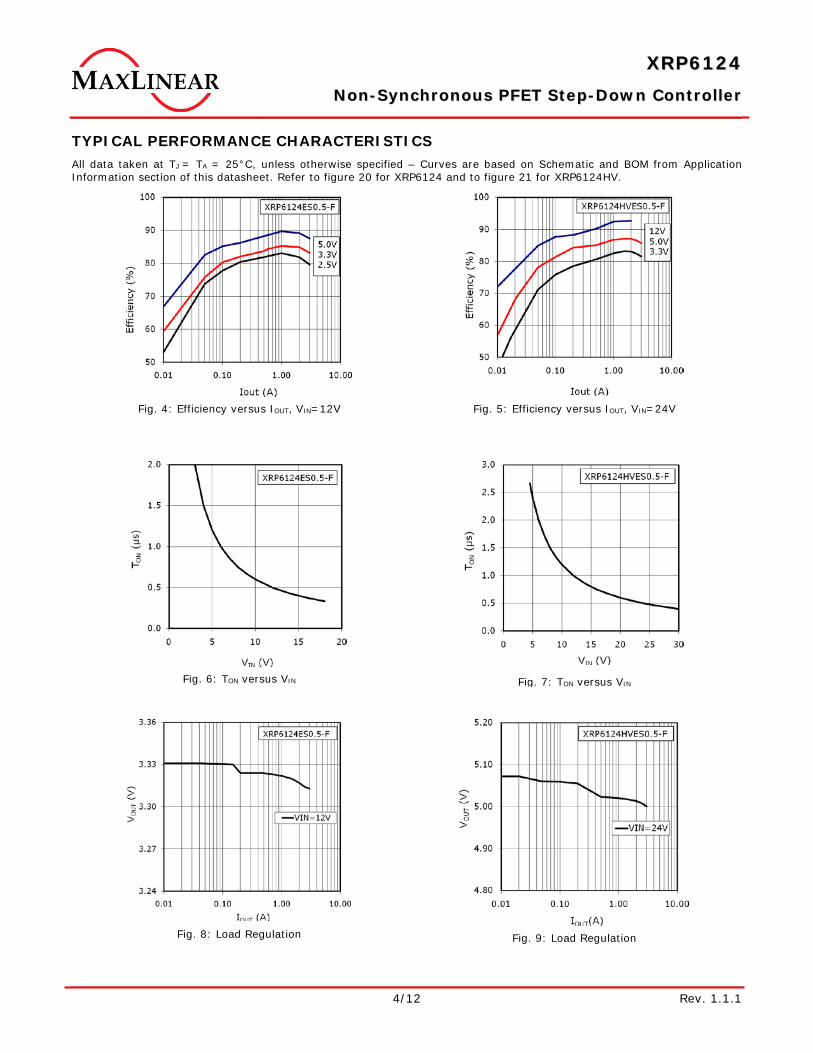
TYPICAL PERFORMANCE CHARACTERISTICS All data taken at TJ = TA = 25°C, unless otherwise specified – Curves are based on Schematic and BOM from Application Information section of this datasheet. Refer to figure 20 for XRP6124 and to figure 21 for XRP6124HV.
Fig. 4: Efficiency versus IOUT, VIN=12V
Fig. 5: Efficiency versus IOUT, VIN=24V
Fig. 6: TON versus VIN
Fig. 7: TON versus VIN
Fig. 8: Load Regulation
Fig. 9: Load Regulation

XXRRPP66112244 NNoonn--SSyynncchhrroonnoouuss PPFFEETT SStteepp--DDoowwnn CCoonnttrroolllleerr
5/12 Rev. 1.1.1
Fig. 10: Line Regulation
Fig. 11: Line Regulation
Fig. 12: Steady state, VIN = 12V, VOUT = 3.3V, IOU T= 3A
Fig. 13: Steady state, VIN = 24V, VOUT = 5.0V, IOUT = 3A
Fig. 14: Load step transient response, 1.4A-3A-1.4A
Fig. 15: Load step transient response, 1.4A-3A-1.4A
XRP6124HVES0.5-F XRP6124ES0.5-F VOUT AC coupled 10mV/div
LX 10V/div
IL 2A/div
LX 20V/div
VOUT AC coupled 20mV/div
IL 2A/div
XRP6124ES0.5-F
1µs/div 2µs/div
XRP6124ES0.5-F XRP6124HVES0.5-F
VOUT AC coupled 100mV/div
VOUT AC coupled 200mV/div
IOUT 1A/div
IOUT 1A/div
10µs/div 20µs/div
90mV 180mV
XXRRPP66112244 NNoonn--SSyynncchhrroonnoouuss PPFFEETT SStteepp--DDoowwnn CCoonnttrroolllleerr
6/12 Rev. 1.1.1
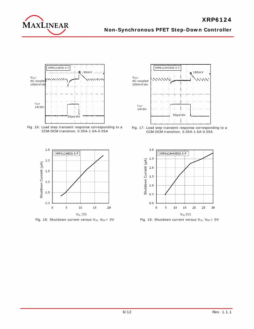
Fig. 16: Load step transient response corresponding to a
CCM-DCM transition, 0.05A-1.6A-0.05A
Fig. 17: Load step transient response corresponding to a
CCM-DCM transition, 0.05A-1.6A-0.05A
Fig. 18: Shutdown current versus VIN, VEN = 0V
Fig. 19: Shutdown current versus VIN, VEN = 0V
XRP6124ES0.5-F XRP6124HVES0.5-F
VOUT AC coupled 100mV/div
VOUT AC coupled 200mV/div
IOUT 1A/div IOUT
1A/div
50µs/div 50µs/div
90mV 180mV
XXRRPP66112244 NNoonn--SSyynncchhrroonnoouuss PPFFEETT SStteepp--DDoowwnn CCoonnttrroolllleerr
7/12 Rev. 1.1.1
THEORY OF OPERATION
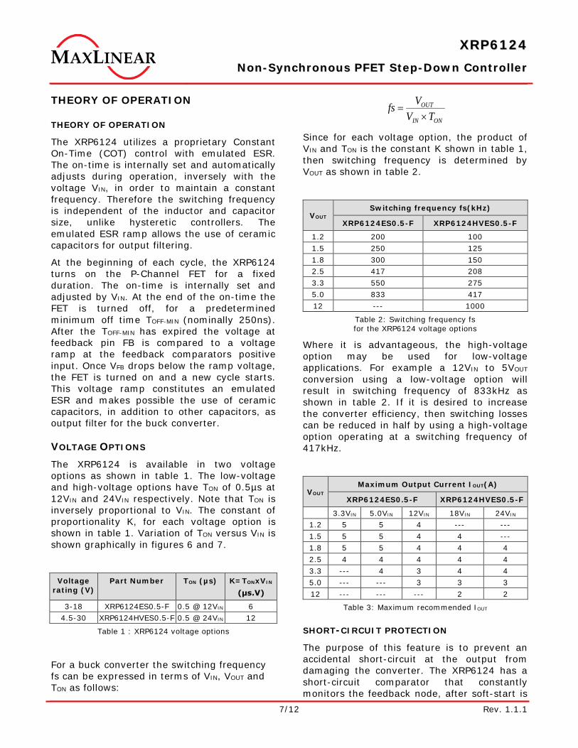
THEORY OF OPERATION The XRP6124 utilizes a proprietary Constant On-Time (COT) control with emulated ESR. The on-time is internally set and automatically adjusts during operation, inversely with the voltage VIN, in order to maintain a constant frequency. Therefore the switching frequency is independent of the inductor and capacitor size, unlike hysteretic controllers. The emulated ESR ramp allows the use of ceramic capacitors for output filtering.
At the beginning of each cycle, the XRP6124 turns on the P-Channel FET for a fixed duration. The on-time is internally set and adjusted by VIN. At the end of the on-time the FET is turned off, for a predetermined minimum off time TOFF-MIN (nominally 250ns). After the TOFF-MIN has expired the voltage at feedback pin FB is compared to a voltage ramp at the feedback comparators positive input. Once VFB drops below the ramp voltage, the FET is turned on and a new cycle starts. This voltage ramp constitutes an emulated ESR and makes possible the use of ceramic capacitors, in addition to other capacitors, as output filter for the buck converter.
VOLTAGE OPTIONS The XRP6124 is available in two voltage options as shown in table 1. The low-voltage and high-voltage options have TON of 0.5µs at 12VIN and 24VIN respectively. Note that TON is inversely proportional to VIN. The constant of proportionality K, for each voltage option is shown in table 1. Variation of TON versus VIN is shown graphically in figures 6 and 7.
Voltage rating (V)
Part Number TON (µs) K=TONxVIN
(μs.V)
3-18 XRP6124ES0.5-F 0.5 @ 12VIN 6 4.5-30 XRP6124HVES0.5-F 0.5 @ 24VIN 12
Table 1 : XRP6124 voltage options
For a buck converter the switching frequency fs can be expressed in terms of VIN, VOUT and TON as follows:
ONIN
OUT
TVVfs×
=
Since for each voltage option, the product of VIN and TON is the constant K shown in table 1, then switching frequency is determined by VOUT as shown in table 2.
VOUT Switching frequency fs(kHz)
XRP6124ES0.5-F XRP6124HVES0.5-F
1.2 200 100 1.5 250 125 1.8 300 150 2.5 417 208 3.3 550 275 5.0 833 417 12 --- 1000
Table 2: Switching frequency fs for the XRP6124 voltage options
Where it is advantageous, the high-voltage option may be used for low-voltage applications. For example a 12VIN to 5VOUT conversion using a low-voltage option will result in switching frequency of 833kHz as shown in table 2. If it is desired to increase the converter efficiency, then switching losses can be reduced in half by using a high-voltage option operating at a switching frequency of 417kHz.
VOUT Maximum Output Current IOUT(A)
XRP6124ES0.5-F XRP6124HVES0.5-F
3.3VIN 5.0VIN 12VIN 18VIN 24VIN 1.2 5 5 4 --- --- 1.5 5 5 4 4 --- 1.8 5 5 4 4 4 2.5 4 4 4 4 4 3.3 --- 4 3 4 4 5.0 --- --- 3 3 3 12 --- --- --- 2 2
Table 3: Maximum recommended IOUT
SHORT-CIRCUIT PROTECTION The purpose of this feature is to prevent an accidental short-circuit at the output from damaging the converter. The XRP6124 has a short-circuit comparator that constantly monitors the feedback node, after soft-start is

XXRRPP66112244 NNoonn--SSyynncchhrroonnoouuss PPFFEETT SStteepp--DDoowwnn CCoonnttrroolllleerr
8/12 Rev. 1.1.1
finished. If the feedback voltage drops below 0.55V, equivalent to output voltage dropping below 69% of nominal, the comparator will trip causing the IC to latch off. In order to restart the XRP6124, the input voltage has to be reduced below UVLO threshold and then increased to its normal operating point.
SOFT-START To limit in-rush current the XRP6124 has an internal soft-start. The nominal soft-start time is 2ms and commences when VIN exceeds the UVLO threshold. As explained above, the short-circuit comparator is enabled as soon as soft-start is complete. Therefore if the input voltage has a very slow rising edge such that at the end of soft-start the output voltage has not reached 69% of its final value then the XRP6124 will latch-off.
ENABLE By applying a logic-level signal to the enable pin EN the XRP6124 can be turned on and off. Pulling the enable below 1V shuts down the controller and reduces the VIN leakage current to 1.5µA nominal as seen in figure 18. Enable signal should always be applied after the input voltage or concurrent with it. Otherwise
XRP6124 will latch up. In applications where an independent enable signal is not available, a Zener diode can be used to derive VEN from VIN.
DISCONTINUOUS CONDUCTION MODE, DCM Because XRP6124 is a non-synchronous controller, when load current IOUT is reduced to less than half of peak-to-peak inductor current ripple ΔIL, the converter enters DCM mode of operation. The switching frequency fs is now IOUT dependent and no longer governed by the relationship shown in table 2. As IOUT is decreased so does fs until a minimum switching frequency, typically in the range of few hundred Hertz, is reached at no load. This contributes to good converter efficiency at light load as seen in figures 4 and 5. The reduced fs corresponding to light load, however, increases the output voltage ripple and causes a slight increase in output voltage as seen in figures 8 and 9. Another effect of reduced fs at light load is slow down of transient response when a load step transitions from a high load to a light load. This is shown in figures 16 and 17.
APPLICATION INFORMATION
SETTING THE OUTPUT VOLTAGE Use an external resistor divider to set the output voltage. Program the output voltage from:
−×= 1
8.021 OUTV
RR
where:
R1 is the resistor between VOUT and FB
R2 is the resistor between FB and GND (nominally 2kΩ)
0.8V is the nominal feedback voltage.
FEED-FORWARD CAPACITOR CFF CFF, which is placed in parallel with R1, provides a low-impedance/high-frequency path for the output voltage ripple to be transmitted to FB. It also helps get an optimum transient response. An initial value for CFF can be calculated from:
11.021
RfsCFF
××××=
π where:
fs is the switching frequency from table 2
This value can be adjusted as necessary to provide an optimum load step transient response.
XXRRPP66112244 NNoonn--SSyynncchhrroonnoouuss PPFFEETT SStteepp--DDoowwnn CCoonnttrroolllleerr
9/12 Rev. 1.1.1
OUTPUT INDUCTOR Select the output inductor L1 for inductance L, DC current rating IDC and saturation current rating ISAT. IDC should be larger than regulator output current. ISAT, as a rule of thumb, should be 50% higher than the regulator output current. Calculate the inductance from:
( )
××∆
−=INL
OUTOUTIN VfsI
VVVL
Where:
ΔIL is peak-to-peak inductor current ripple nominally set to 30% of IOUT
fS is nominal switching frequency from table 2
OUTPUT CAPACITOR COUT Select the output capacitor for voltage rating, capacitance COUT and Equivalent Series Resistance ESR. The voltage rating, as a rule of thumb, should be twice the output voltage. When calculating the required capacitance, usually the overriding requirement is current load-step transient. If the unloading transient requirement (i.e., when IOUT transitions from a high to a low current) is met, then usually the loading transient requirement (when IOUT transitions from a low to a high current) is met as well. Therefore calculate the COUT capacitance based on the unloading transient requirement from:
( )
−+
−×= 22
22
OUTtransientOUT
LOWHighOUT VVV
IILC
Where:
L is the inductance calculated in the preceding step
IHigh is the value of IOUT prior to unloading. This is nominally set equal to regulator current rating.
ILow is the value of IOUT after unloading. This is nominally set equal to 50% of regulator current rating.
Vtransient is the maximum permissible voltage transient corresponding to the load step mentioned above. Vtransient is typically specified from 3% to 5% of VOUT.
ESR of the capacitor has to be selected such that the output voltage ripple requirement VOUT(ripple), nominally 1% of VOUT, is met. Voltage ripple VOUT(ripple) is composed mainly of two components: the resistive ripple due to ESR and capacitive ripple due to COUT charge transfer. For applications requiring low voltage ripple, ceramic capacitors are recommended because of their low ESR which is typically in the range of 5mΩ. Therefore VOUT(ripple) is mainly capacitive. For ceramic capacitors calculate the VOUT(ripple) from:
fsCI
OUT
L
××∆
=8
V )OUT(ripple
Where:
COUT is the value calculated above
If tantalum or electrolytic capacitors are used then VOUT(ripple) is essentially a function of ESR:
ESRIL ×∆= V )OUT(ripple
INPUT CAPACITOR CIN Select the input capacitor for voltage rating, RMS current rating and capacitance. The voltage rating, as a rule of thumb, should be 50% higher than the regulator’s maximum input voltage. Calculate the capacitor’s current rating from:
( )DDIOUT −××= 1 I RMSCIN,
Where:
IOUT is regulator’s maximum current
D is duty cycle (D=VOUT/VIN)
Calculate the CIN capacitance from:
( )ININ
OUTINOUTOUT
VVfsVVVI
∆××−××
= 2INC
Where:
ΔVIN is the permissible input voltage ripple, nominally set to 1% of VIN.
XXRRPP66112244 NNoonn--SSyynncchhrroonnoouuss PPFFEETT SStteepp--DDoowwnn CCoonnttrroolllleerr
10/12 Rev. 1.1.1
TYPICAL APPLICATIONS
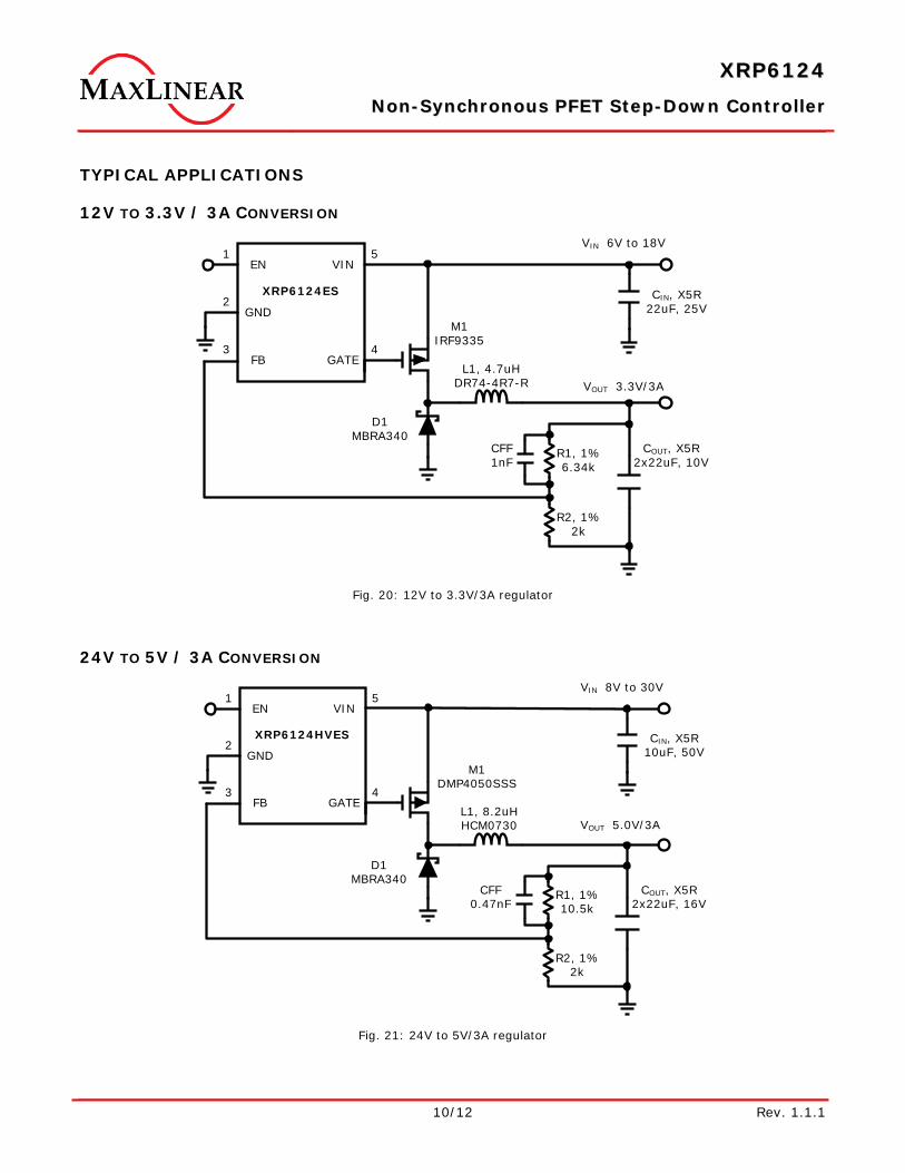
12V TO 3.3V / 3A CONVERSION
XRP6124ES
VIN
GND
GATEFB
EN
D1MBRA340
L1, 4.7uHDR74-4R7-R
M1IRF9335
R1, 1%6.34k
R2, 1%2k
CFF1nF
1
2
3 4
5
COUT, X5R2x22uF, 10V
CIN, X5R22uF, 25V
VIN 6V to 18V
VOUT 3.3V/3A
Fig. 20: 12V to 3.3V/3A regulator
24V TO 5V / 3A CONVERSION
XRP6124HVES
VIN
GND
GATEFB
EN
D1MBRA340
L1, 8.2uHHCM0730
M1DMP4050SSS
R1, 1%10.5k
R2, 1%2k
CFF0.47nF
1
2
3 4
5
COUT, X5R2x22uF, 16V
CIN, X5R10uF, 50V
VIN 8V to 30V
VOUT 5.0V/3A
Fig. 21: 24V to 5V/3A regulator
XXRRPP66112244 NNoonn--SSyynncchhrroonnoouuss PPFFEETT SStteepp--DDoowwnn CCoonnttrroolllleerr
11/12 Rev. 1.1.1
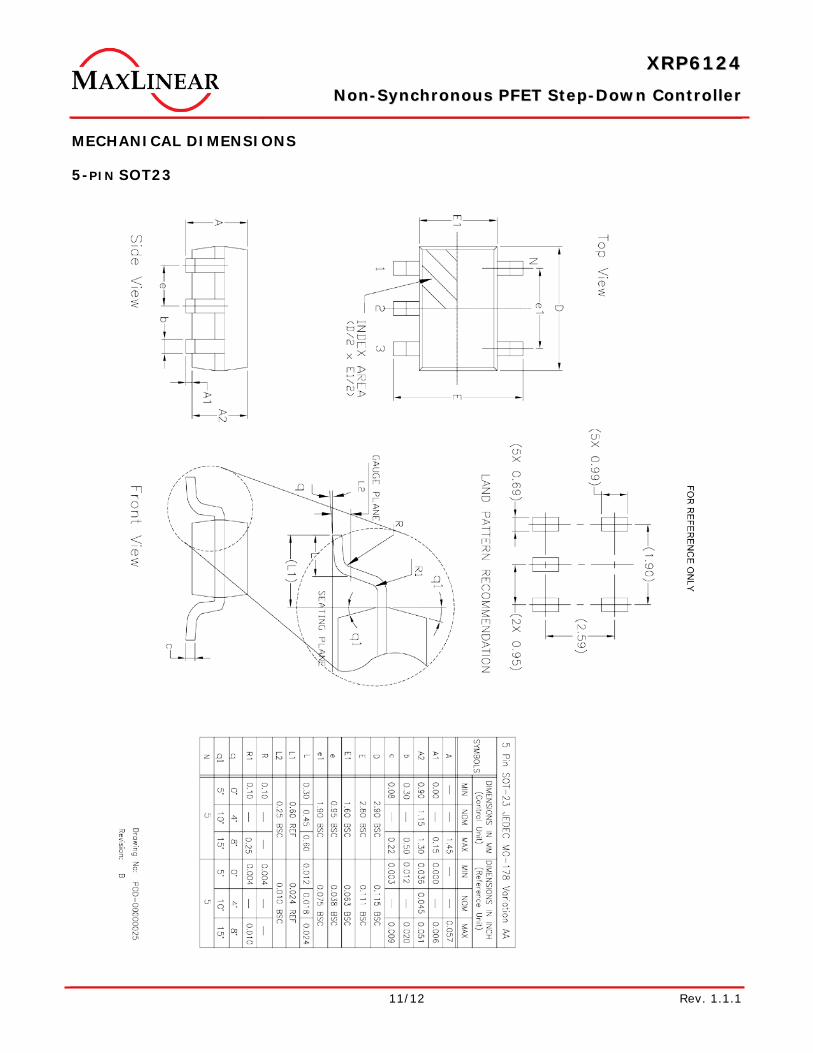
MECHANICAL DIMENSIONS
5-PIN SOT23
XXRRPP66112244 NNoonn--SSyynncchhrroonnoouuss PPFFEETT SStteepp--DDoowwnn CCoonnttrroolllleerr
12/12 Rev. 1.1.1
REVISION HISTORY
Revision Date Description
1.0.0 01/26/2011 Initial release of datasheet 1.1.0 01/31/2011 Corrected typo (changed V to I) on formula under Input Capacitor CIN paragraph 1.1.1 05/24/2018 Updated to MaxLinear logo. Updated format and Ordering Information.
Corporate Headquarters: 5966 La Place Court Suite 100 Carlsbad, CA 92008 Tel.:+1 (760) 692-0711 Fax: +1 (760) 444-8598
www.maxlinear.com
High Performance Analog: 1060 Rincon Circle San Jose, CA 95131 Tel.: +1 (669) 265-6100 Fax: +1 (669) 265-6101
www.exar.com
The content of this document is furnished for informational use only, is subject to change without notice, and should not be construed as a commitment by MaxLinear, Inc.. MaxLinear, Inc. assumes no responsibility or liability for any errors or inaccuracies that may appear in the informational content contained in this guide. Complying with all applicable copyright laws is the responsibility of the user. Without limiting the rights under copyright, no part of this document may be reproduced into, stored in, or introduced into a retrieval system, or transmitted in any form or by any means (electronic, mechanical, photocopying, recording, or otherwise), or for any purpose, without the express written permission of MaxLinear, Inc.
Maxlinear, Inc. does not recommend the use of any of its products in life support applications where the failure or malfunction of the product can reasonably be expected to cause failure of the life support system or to significantly affect its safety or effectiveness. Products are not authorized for use in such applications unless MaxLinear, Inc. receives, in writing, assurances to its satisfaction that: (a) the risk of injury or damage has been minimized; (b) the user assumes all such risks; (c) potential liability of MaxLinear, Inc. is adequately protected under the circumstances.
MaxLinear, Inc. may have patents, patent applications, trademarks, copyrights, or other intellectual property rights covering subject matter in this document. Except as expressly provided in any written license agreement from MaxLinear, Inc., the furnishing of this document does not give you any license to these patents, trademarks, copyrights, or other intellectual property.
Company and product names may be registered trademarks or trademarks of the respective owners with which they are associated.
© 2011 - 2018 MAXLINEAR, INC. ALL RIGHTS RESERVED