nonlinear coss-vds profile based zvs range calculation for
TRANSCRIPT
Aalborg Universitet
Nonlinear Coss-VDS Profile based ZVS Range Calculation for Dual Active BridgeConverters
Liu, Bochen; Davari, Pooya; Blaabjerg, Frede
Published in:I E E E Transactions on Power Electronics
DOI (link to publication from Publisher):10.1109/TPEL.2020.3003248
Publication date:2021
Document VersionAccepted author manuscript, peer reviewed version
Link to publication from Aalborg University
Citation for published version (APA):Liu, B., Davari, P., & Blaabjerg, F. (2021). Nonlinear C
oss-V
DS Profile based ZVS Range Calculation for Dual
Active Bridge Converters. I E E E Transactions on Power Electronics, 36(1), 45-50. [9119872].https://doi.org/10.1109/TPEL.2020.3003248
General rightsCopyright and moral rights for the publications made accessible in the public portal are retained by the authors and/or other copyright ownersand it is a condition of accessing publications that users recognise and abide by the legal requirements associated with these rights.
- Users may download and print one copy of any publication from the public portal for the purpose of private study or research. - You may not further distribute the material or use it for any profit-making activity or commercial gain - You may freely distribute the URL identifying the publication in the public portal -
Take down policyIf you believe that this document breaches copyright please contact us at [email protected] providing details, and we will remove access tothe work immediately and investigate your claim.
0885-8993 (c) 2020 IEEE. Personal use is permitted, but republication/redistribution requires IEEE permission. See http://www.ieee.org/publications_standards/publications/rights/index.html for more information.
This article has been accepted for publication in a future issue of this journal, but has not been fully edited. Content may change prior to final publication. Citation information: DOI 10.1109/TPEL.2020.3003248, IEEETransactions on Power Electronics
IEEE POWER ELECTRONICS LETTER
Nonlinear Coss-VDS Profile based ZVS RangeCalculation for Dual Active Bridge Converters
Bochen Liu, Student Member, IEEE, Pooya Davari, Senior Member, IEEE, Frede Blaabjerg, Fellow, IEEE
Abstract—Generally, power electronic converters are designedto obtain the highest efficiency at rated power while theyare most often operated under partial loading conditions. Fordual active bridge (DAB) converters, the zero-voltage-switching(ZVS) conditions can be impaired under light load situations.While load depending ZVS operation has been introduced byprior-art approaches, the nonlinear characteristic of the outputcapacitance in a power device is often not considered and itseffect on operating boundaries of ZVS is neglected. In this letter,based on practical switching transients, an improved method ofcalculating the ZVS range is introduced. By taking into accountthe non-linearity of output capacitance, the method is developedfrom a detailed analysis of real switching transients. A 2.5 kWprototype is built, and a comprehensive comparison with prior-art approaches is conducted to validate the accuracy of theproposed method.
I. INTRODUCTION
One advantage of the DAB converter [1] is the inherentcapability of naturally achieving ZVS for all switches withoutany auxiliary circuits, and this advantage has facilitated awide application of DAB converters, such as in distributedpower systems [2], energy storage systems [3] and electricvehicles [4]. However, due to the lower leakage inductancecurrent in light-load conditions, the charge stored in thetransistor output capacitor may not be totally released duringthe dead time, and this might result in ZVS failure owingto high voltage across the transistor at the turn-on instant.This failure would further increase the switching losses, impairthe electromagnetic compatibility (EMC) performance [5] andeven damage the power devices [6].
There are two commonly used methods to identify the limi-tations on the control variables for achieving ZVS, i.e. current-based method [7], [8] and energy-based method [9]. Therein,the current-based method is developed from the body diodeconduction when the power device is switched on and thusZVS conditions can be attained by controlling a positive ornegative leakage inductance current at the switching instants.However, the positive/negative current direction is the resultof the ZVS achievement, which is not sufficient to guaranteea soft switching. In respect to the energy-based method, theZVS is achieved under the condition that the energy storedin the output capacitance Coss is totally released before thetransistor is switched on. This method is better by requiring aminimum leakage inductance current at the switching instants.However, the non-linearity of the parasitic output capacitanceis usually not taken into account, in spite of the fact that theoutput capacitance of a power device varies a lot during theturn-on/turn-off procedure. Besides, the calculation procedureis complex regarding the square mathematical operation of
the stored energy(e.g. 1/2Li2). Moreover, due to that moreconverter components are involved in the calculation, a highmodeling accuracy of the involved components (e.g. the trans-former) is required for an accurate ZVS range calculation andthis accurate modeling would further increase the complexity.Consequently, owing to the missing consideration of the non-linearity and the complex calculation procedure, the obtainedZVS range using the method would contain some criticaloperating points that could lead to ZVS failure.
A charge-based ZVS calculation method is proposed in [10],where the nonlinear change of output capacitance is involved.This method can achieve a more accurate ZVS operatingrange, and thus this letter also calculates the ZVS range basedon the charge balance. But compared to the method in [10],the main difference and improvements of the proposed methodin this letter are listed in the following.
Firstly, the calculation of the available charges in [10] is notappropriate. In [10], the integration of the bridge current startsfrom the zero-crossing time instants to the switching moment,and the results are compared with the required discharge ofthe output capacitance. However, the time range between thetwo zero-crossing instants [10] might not be the dischargingtime interval of the output capacitance. In practical switchingtransients (cf. Section II), the actual integration limits shouldstart from the instant when the drain-source voltage begin toreduce, and end at the instant when the drain-source voltagebecomes zero. The whole discharging interval is within thisstarting point and ending point, during which the discharge ofthe output capacitance synchronizes with the charge movementin the bridge current. Hence, this discharging interval is theproper integration interval for calculating the conveyed chargesby the bridge current. Actually, this discharging interval isequal to the dead time, and it is not involved in the chargecalculation in [10]. More details can be found in Section IV.
Secondly, the half dc-bus voltage change consideration in[10] is not appropriate because the drain-source voltage of apower device will switch between zero and the whole dc-busvoltage during transients. The turn-on of one power devicecorresponds to the turn-off of the other one at the same time.Therefore, the charge and discharge of the power devices inthe same bridge leg are analyzed together (Section III) in thispaper.
In this letter, a nonlinear Coss profile based ZVS range cal-culation method is presented according to practical switchingtransients in a DAB converter. Notably, this method can beapplied to the full load range, but due to that the DAB iseasier to lose ZVS in light load, this letter will focus onlight-load operation. The measured switching transients are
Authorized licensed use limited to: Aalborg Universitetsbibliotek. Downloaded on June 26,2020 at 06:32:43 UTC from IEEE Xplore. Restrictions apply.

0885-8993 (c) 2020 IEEE. Personal use is permitted, but republication/redistribution requires IEEE permission. See http://www.ieee.org/publications_standards/publications/rights/index.html for more information.
This article has been accepted for publication in a future issue of this journal, but has not been fully edited. Content may change prior to final publication. Citation information: DOI 10.1109/TPEL.2020.3003248, IEEETransactions on Power Electronics
IEEE POWER ELECTRONICS LETTER
Fig. 1. Circuit topology of a DAB converter with full-bridges FB1 and FB2.
Fig. 2. Operation of the DAB converter (a) Typical operation mode charac-terized by αp, αs and ϕ. (b) General MOSFET model and resultant circuitstate of the full-bridge FB1 during the turn-on of Q4.
Fig. 3. A detailed description of the three control variables αp, αs and ϕ inpractical control.
firstly shown in Section II. Then ZVS analysis concerningthe nonlinear change of the output capacitance is conductedin Section III. Next, a comparative analysis with other ZVScalculation methods is presented and verified by experimentalresults in Section IV, including a comparison with the charge-based method proposed in [10]. At the end, the conclusionsare summarized.
II. PRACTICAL SWITCHING TRANSIENTS
A DAB converter topology is shown in Fig. 1. It mainlyconsists of two full-bridges (i.e. FB1 and FB2) generatinga two-level or three-level ac voltage (i.e. vp and vs) acrossthe transformer-inductor combination. A generalized light-load modulation method [11] is applied and relevant workingwaveforms are as shown in Fig. 2(a). Therein, three controlvariables are used to regulate the converter, i.e. duty cycles(αp, αs) of vp, vs and the phase shift angle (ϕ) between the
TABLE ISYSTEM PARAMETERS OF A DAB PROTOTYPE
Parameter Variable Value
Input DC voltage V1 200 VOutput DC voltage V2 35 VTurns ratio of the transformer n : 1 3.5 : 1Switching frequency fsw 60 kHzLeakage inductance L 45 µH
Fig. 4. Measured transient drain-source voltages and gate-source voltages ofQ4 at turning on. Control parameters: αp = 60◦, αs = 110◦, and ϕ =3◦, 4◦, 5◦...10◦ in the 8 cases, respectively.
fundamental components of these two voltages. It is commonthat a dead time Tdead is inserted between the two powerdevices in the same leg (e.g. Q2 and Q4) to avoid short circuit.As a result, this might cause ϕ to drift in practical control,and hence the dead time effect on the control variables shouldbe considered and properly compensated [12], [13]. In thispaper, by using the dead time compensation methods in [12],the practical control variables are depicted in details as shownin Fig. 3.
As highlighted in Fig. 2(a), the power device Q4 is turnedon at t = t3, and meanwhile, Q2 is turned off and Q1 is kepton. Consequently, the transient turning on procedure of Q4
can be described by the FB1 transition circuit in Fig. 2(b). Ina MOSFET device, parasitic capacitances are coupled amongthe drain, source and gate terminals, denoted by CGD, CGS
and CDS in Fig. 2(b). On this basis, a nonlinear characteristicdefined by Coss = CGD + CDS is often used to analyze thedynamic switching procedure (cf. Section III).
Using V1 = 200 V from a dc power source, the measuredtransient drain-source voltages and gate-source voltages of Q4
and leakage inductance currents are shown in Fig. 4. Thekey experimental parameters of the DAB setup are listed inTable I. In Fig. 4, there are 8 groups of VDS,Q4 and VGS,Q4
corresponding to the phase shift ϕ varying from 3◦ to 10◦. The
Authorized licensed use limited to: Aalborg Universitetsbibliotek. Downloaded on June 26,2020 at 06:32:43 UTC from IEEE Xplore. Restrictions apply.
0885-8993 (c) 2020 IEEE. Personal use is permitted, but republication/redistribution requires IEEE permission. See http://www.ieee.org/publications_standards/publications/rights/index.html for more information.
This article has been accepted for publication in a future issue of this journal, but has not been fully edited. Content may change prior to final publication. Citation information: DOI 10.1109/TPEL.2020.3003248, IEEETransactions on Power Electronics
IEEE POWER ELECTRONICS LETTER
used power device Q4 is Infineon IPW65R080CFD, and thethreshold voltage VGS(th) = 4 V can be read from the datasheetor manually measured. During the interval t ∈ [0.2 µs, 0.6 µs],VDS,Q4 decreases from V1 to 0 due to the discharge of out-put capacitance Coss,Q4. In the meantime, VGS,Q4 graduallyincreases and when it reaches VGS(th), the transistor is turnedon. Hence, if the drain-source voltage has been reduced to zeroor near-zero at this instant, ZVS can be achieved. Otherwise,it transfers to hard switching if VDS,Q4 is still relatively high,and VGS,Q4 starts to oscillate. In conclusion, in order to realizezero voltage switching of Q4, the output capacitance Coss,Q4
should be sufficiently discharged.
III. IMPLEMENTATION OF NONLINEAR COSS-VDS PROFILEIN ZVS ANALYSIS
As concluded from the practical switching transients in thelast section, the charges stored in the output capacitance shouldbe fully released before turning on in order to achieve ZVS.Hence, in order to obtain an accurate ZVS range, firstly thestored charges should be properly calculated with varying VDS
and non-linear Coss. Regarding this, the Coss trajectory hardlyvaries with the temperature for Si super-junction [14], widebandgap SiC [15] and GaN [16] devices, and thus the non-linear Coss−VDS profile can be adopted to calculate the storedcharges.
As shown in Fig. 2(b), the transient voltages VDS,Q2 andVDS,Q4 can be described by
Coss,Q2dVDS,Q2
dt= −iD,Q2
Coss,Q4dVDS,Q4
dt= iD,Q4
(1)
where iD,Q2 and iD,Q4 are the drain currents of Q2 and Q4,respectively. Combining (1) with the following relationship{
iD,Q4 + iD,Q2 = ip
VDS,Q4 + VDS,Q2 = V1(2)
leads toip =
[Coss,Q2 + Coss,Q4
]dVDS,Q4
dt(3)
For simplification, an equivalent capacitance Ceq defined as
Ceq = Coss(V1 − VDS,Q4) + Coss(VDS,Q4) (4)
is introduced to replace the term Coss,Q2+Coss,Q4 in (3). Thevalues of Coss(V1−VDS,Q4) and Coss(VDS,Q4) in (4) can beextracted from the nonlinear Coss−VDS profile shown in Fig.5(a), which is usually given in the datasheet. Therefore, theCeq trajectory can be obtained as shown in Fig. 5(b).
The equivalent charge Qeq stored in Ceq with an off-statedrain-source voltage V1 can be calculated by
Qeq =
∫ V1
0
CeqdVDS (5)
The patched area in Fig. 5(b) denotes the charge quantity withV1 = 200 V.
On the other hand, another condition for ZVS is that thestored charges Qeq can be fully released into the leakageinductance current ip, which means the conveyed charges in
(a) (b)
Fig. 5. Nonlinear profiles of (a) Coss, (b) Ceq along with VDS for InfineonIPW65R080CFD.
Fig. 6. Measured leakage inductance currents ip with ϕ = 3◦ ∼ 10◦ andsource-drain voltages VDS,Q4 with ϕ = 6◦, 10◦ at the turn-on of Q4. Thelighter and darker patched areas are the conveyed charges Qip by ip in thecases of ϕ = 6◦ and ϕ = 10◦, respectively.
Fig. 7. Numerical integration (i.e. marked lines) of the measured currents ipand the transient charge of Ceq (i.e. solid line) as the drain-source voltage ofQ4 reversely changes from 0 V to 200 V.
ip should be larger than Qeq . The total charges Qip in ipat the turning on of Q4 could be represented by the patchedareas in Fig. 6. Therein, the lighter patched area denotes Qip
in the case of ϕ = 6◦ and the darker is Qip in the case ofϕ = 10◦. It can be seen that the value of Qip decreases as ϕis increased from 3◦ to 10◦. For the convenience of analysis,t = 0.6 µs is deemed the time origin and t = 0.2 µs thetransient ending. Therefore, the transient charge Q conveyedby ip during change of VDS can be calculated by using anumerical integration technique. Corresponding to different ϕ,the trajectories of Q are shown by different marked lines inFig. 7. Note that Q is equal to the total charge Qip when VDS
reaches 200 V. As a comparison, the transient charge storedin the equivalent output capacitance Ceq is also shown in Fig.7, denoted by the solid line with a final value of Qeq (cf. Fig.
Authorized licensed use limited to: Aalborg Universitetsbibliotek. Downloaded on June 26,2020 at 06:32:43 UTC from IEEE Xplore. Restrictions apply.
0885-8993 (c) 2020 IEEE. Personal use is permitted, but republication/redistribution requires IEEE permission. See http://www.ieee.org/publications_standards/publications/rights/index.html for more information.
This article has been accepted for publication in a future issue of this journal, but has not been fully edited. Content may change prior to final publication. Citation information: DOI 10.1109/TPEL.2020.3003248, IEEETransactions on Power Electronics
IEEE POWER ELECTRONICS LETTER
5(b)).In the case of ϕ = 10◦, the available charge Qip = 0.4 µC
in the current is lower than the stored charge Qeq = 0.58 µCin the equivalent capacitance, indicating an insufficient dis-charge of Ceq . Hence, VDS,Q4 sharply drops from 115 V to0 V in less than 0.1 µs (cf. Fig. 4) and severe oscillationsare induced in the leakage inductance current. This non-ZVScase should be avoided since it might increase the switchinglosses and even potentially break the power device [6] due tohigh dv/dt. In cases of ϕ = 3◦...7◦, the charge Qip is largerthan Qeq , e.g. Qip = 0.67 µC with ϕ = 6◦. Therefore, theequivalent capacitance Ceq can be totally discharged before Q4
is turned on. In terms of the middle cases where ϕ = 8◦, 9◦,the transferred charge Qip (equals 0.48 µC with ϕ = 9◦)by the current is a bit lower than Qeq , also implying aninsufficient discharge of Ceq . One difference from the 10◦
case is that the drain-source voltage of Q4 has reduced toa sufficient low level at turning on, e.g. 45 V for ϕ = 9◦
and even lower for ϕ = 8◦ (cf. Fig. 4). Thus no obviousoscillations are stimulated and they are named as quasi-ZVS inFig. 7. Due to that the switching losses are increased in quasi-ZVS cases (i.e. ϕ = 8◦, 9◦) and the power devices could beimpaired in non-ZVS cases (i.e. ϕ = 10◦), the ZVS is regardedfailed in the quasi-ZVS and non-ZVS cases.
IV. ZVS RANGE COMPARISON WITH EXPERIMENTALVALIDATION
There are mainly three approaches to derive the ZVS rangein literature, named as App1, App2 and App3 in the following,and the proposed ZVS range calculation method is representedby Pro..
App1: The most often used method [7] to calculate the ZVSconditions is by
I3 =nV2
4πLfsw
[(k − 1)αp − 2ϕ
]≥ 0 → αp ≥
2
k − 1ϕ (6)
where k = V1/(nV2) is the input/output dc voltage ratio andfsw is the switching frequency.
App2: Another conventional method [9], [17] to calculatethe ZVS conditions is focusing on the energy exchange,leading to
αp ≥2
k − 1ϕ+
4πLfsw(k − 1)nV2
√| 4nCV1V2 − 2CV 2
1 |L
(7)
where C = 1/V1∫ V1
0CossdVDS . In this energy-based method,
other than the missing consideration of the non-linearity ofthe output capacitance, the calculation is complex and it isdifficult to achieve the same accuracy as the proposed method.This is because more converter components are involved in thederivation [17], and the calculation will become even morecomplex if the non-linear Coss is considered.
App3: A third method in [10] is comparing the storedcharges Qcoss in Coss,Q4 (i.e. Qcoss =
∫ V1
0CossdVDS) with
the two defined charges QA and QB as shown in Fig. 8(a),resulting in{
QA = −∫ txy
txipdt ≥ Qcoss
QB = −∫ tytxy
ipdt ≥ Qcoss
=⇒
αp ≥ max.
2
k − 1ϕ+
4πfswk − 1
√LQeq
nV2,
2
k − 1ϕ+
4πfswk − 1
√(k − 1)LQeq
nV2
(8)
Although the non-linearity of the output capacitance isincluded in this method, the integration limits are not properlyconsidered. As comparison, the integration limits of App3 andthe proposed method are depicted in Fig. 8(b), represented bytx, ty and t1, t2, respectively. It can be seen from Fig. 8(b) thatthe discharging procedure of the output capacitance of Q4 iscompleted within [t1, t2], which means that this procedure hasnot began at t = tx and has finished at t = ty . Therefore, theinvolved ranges of [tx, t1] and [t2, ty] in the calculation (cf.(8)) of the conveyed charges of ip in App3 is not appropriate.As a result, although the calculated QA and QB{
QA = 0.36 µC > Qcoss = 0.29 µC
QB = 0.44 µC > Qcoss = 0.29 µC(9)
satisfy the ZVS conditions (8) in App3, the soft switchingactually fails in the operating case of ϕ = 10◦ as in shownFig. 8(a) .
Pro.: Based on the ZVS analysis in Section III, the proposedmethod of deriving ZVS condition is to compare the storedcharges in the equivalent capacitance Ceq with the conveyedcharges in current ip during transients, i.e.
Qip = −∫ Tdead
0
ipdt ≥ Qeq =
∫ V1
0
CeqdVDS (10)
The time 0 → Tdead in (10) (cf. Fig. 8(b)) can be mappedto 0.6 µs→ 0.2 µs in Fig. 6. For comparing with App3, thecalculated Qip and Qeq are
Qip = 0.4 µC < Qeq = 0.58 µC (11)
and it does not satisfy the ZVS condition (10) of the proposedmethod, which is consistent with the failed ZVS case in Fig.8(b).
As discussed in Section III (cf. Fig. 7), the boundary ZVScase is at ϕ = 7◦. Seen from the practical ip waveform in thecase of ϕ = 7◦ in Fig. 6, an approximate method to estimateQip is by dividing the transient procedure into two intervals
ip =
−I3, t ∈
[0,Tdead2
)−I3 +
nV2L
(t− Tdead
2
), t ∈
[Tdead2
, Tdead
] (12)
where 0→ Tdead/2 corresponds to 0.6 µs→ 0.4 µs in Fig. 6and Tdead/2→ Tdead is 0.4 µs→ 0.2 µs. In other words, thevalue of ip is approximated as constant −I3 in the first half ofthe dead time and a linear change in the second half. Hence,the ZVS limitation can be further derived by combining (10)and (12), resulting in
αp ≥2
k − 1ϕ+
4πLfsw(k − 1)nV2
[ Qeq
Tdead+nV28L
Tdead
](13)
Authorized licensed use limited to: Aalborg Universitetsbibliotek. Downloaded on June 26,2020 at 06:32:43 UTC from IEEE Xplore. Restrictions apply.
0885-8993 (c) 2020 IEEE. Personal use is permitted, but republication/redistribution requires IEEE permission. See http://www.ieee.org/publications_standards/publications/rights/index.html for more information.
This article has been accepted for publication in a future issue of this journal, but has not been fully edited. Content may change prior to final publication. Citation information: DOI 10.1109/TPEL.2020.3003248, IEEETransactions on Power Electronics
IEEE POWER ELECTRONICS LETTER
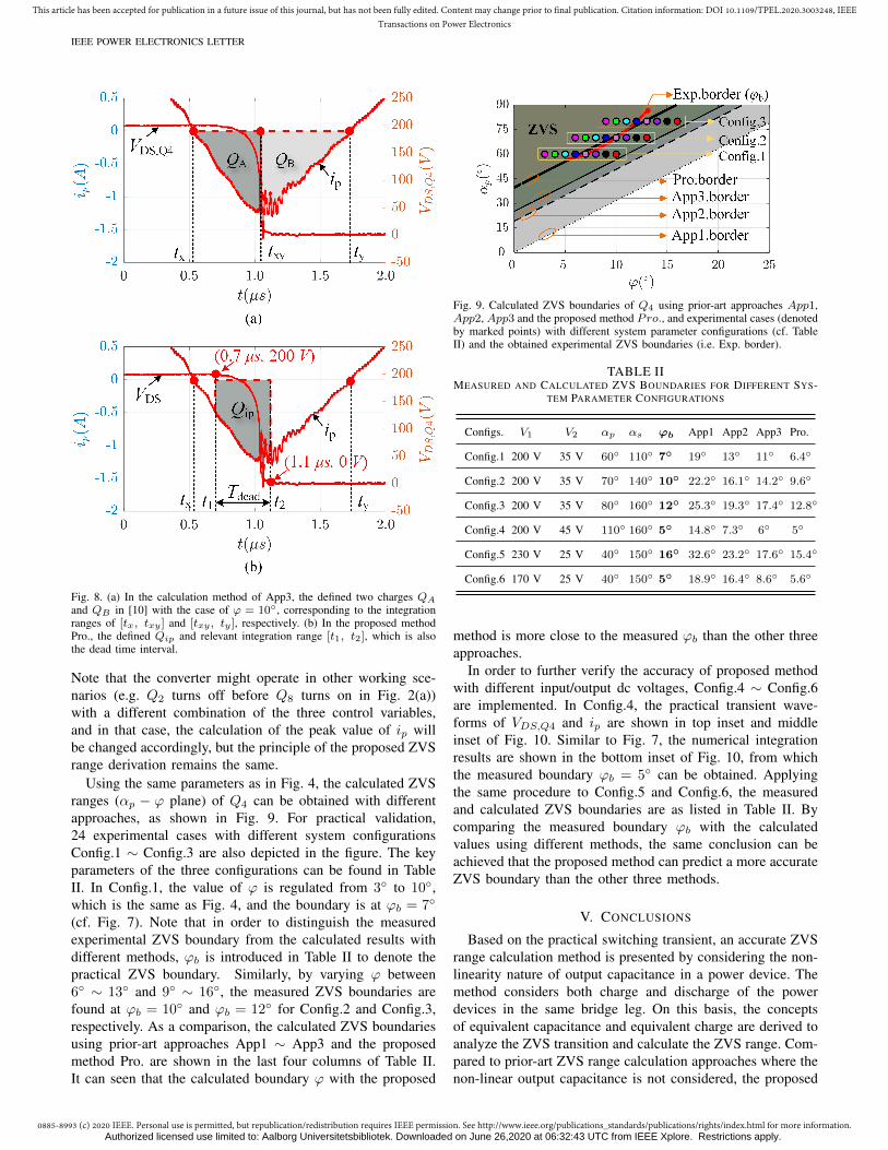
Fig. 8. (a) In the calculation method of App3, the defined two charges QA
and QB in [10] with the case of ϕ = 10◦, corresponding to the integrationranges of [tx, txy ] and [txy , ty ], respectively. (b) In the proposed methodPro., the defined Qip and relevant integration range [t1, t2], which is alsothe dead time interval.
Note that the converter might operate in other working sce-narios (e.g. Q2 turns off before Q8 turns on in Fig. 2(a))with a different combination of the three control variables,and in that case, the calculation of the peak value of ip willbe changed accordingly, but the principle of the proposed ZVSrange derivation remains the same.
Using the same parameters as in Fig. 4, the calculated ZVSranges (αp − ϕ plane) of Q4 can be obtained with differentapproaches, as shown in Fig. 9. For practical validation,24 experimental cases with different system configurationsConfig.1 ∼ Config.3 are also depicted in the figure. The keyparameters of the three configurations can be found in TableII. In Config.1, the value of ϕ is regulated from 3◦ to 10◦,which is the same as Fig. 4, and the boundary is at ϕb = 7◦
(cf. Fig. 7). Note that in order to distinguish the measuredexperimental ZVS boundary from the calculated results withdifferent methods, ϕb is introduced in Table II to denote thepractical ZVS boundary. Similarly, by varying ϕ between6◦ ∼ 13◦ and 9◦ ∼ 16◦, the measured ZVS boundaries arefound at ϕb = 10◦ and ϕb = 12◦ for Config.2 and Config.3,respectively. As a comparison, the calculated ZVS boundariesusing prior-art approaches App1 ∼ App3 and the proposedmethod Pro. are shown in the last four columns of Table II.It can seen that the calculated boundary ϕ with the proposed
Fig. 9. Calculated ZVS boundaries of Q4 using prior-art approaches App1,App2, App3 and the proposed method Pro., and experimental cases (denotedby marked points) with different system parameter configurations (cf. TableII) and the obtained experimental ZVS boundaries (i.e. Exp. border).
TABLE IIMEASURED AND CALCULATED ZVS BOUNDARIES FOR DIFFERENT SYS-
TEM PARAMETER CONFIGURATIONS
Configs. V1 V2 αp αs ϕb App1 App2 App3 Pro.
Config.1 200 V 35 V 60◦ 110◦ 7◦ 19◦ 13◦ 11◦ 6.4◦
Config.2 200 V 35 V 70◦ 140◦ 10◦ 22.2◦ 16.1◦ 14.2◦ 9.6◦
Config.3 200 V 35 V 80◦ 160◦ 12◦ 25.3◦ 19.3◦ 17.4◦ 12.8◦
Config.4 200 V 45 V 110◦ 160◦ 5◦ 14.8◦ 7.3◦ 6◦ 5◦
Config.5 230 V 25 V 40◦ 150◦ 16◦ 32.6◦ 23.2◦ 17.6◦ 15.4◦
Config.6 170 V 25 V 40◦ 150◦ 5◦ 18.9◦ 16.4◦ 8.6◦ 5.6◦
method is more close to the measured ϕb than the other threeapproaches.
In order to further verify the accuracy of proposed methodwith different input/output dc voltages, Config.4 ∼ Config.6are implemented. In Config.4, the practical transient wave-forms of VDS,Q4 and ip are shown in top inset and middleinset of Fig. 10. Similar to Fig. 7, the numerical integrationresults are shown in the bottom inset of Fig. 10, from whichthe measured boundary ϕb = 5◦ can be obtained. Applyingthe same procedure to Config.5 and Config.6, the measuredand calculated ZVS boundaries are as listed in Table II. Bycomparing the measured boundary ϕb with the calculatedvalues using different methods, the same conclusion can beachieved that the proposed method can predict a more accurateZVS boundary than the other three methods.
V. CONCLUSIONS
Based on the practical switching transient, an accurate ZVSrange calculation method is presented by considering the non-linearity nature of output capacitance in a power device. Themethod considers both charge and discharge of the powerdevices in the same bridge leg. On this basis, the conceptsof equivalent capacitance and equivalent charge are derived toanalyze the ZVS transition and calculate the ZVS range. Com-pared to prior-art ZVS range calculation approaches where thenon-linear output capacitance is not considered, the proposed
Authorized licensed use limited to: Aalborg Universitetsbibliotek. Downloaded on June 26,2020 at 06:32:43 UTC from IEEE Xplore. Restrictions apply.

0885-8993 (c) 2020 IEEE. Personal use is permitted, but republication/redistribution requires IEEE permission. See http://www.ieee.org/publications_standards/publications/rights/index.html for more information.
This article has been accepted for publication in a future issue of this journal, but has not been fully edited. Content may change prior to final publication. Citation information: DOI 10.1109/TPEL.2020.3003248, IEEETransactions on Power Electronics
IEEE POWER ELECTRONICS LETTER
Fig. 10. Measured transients of VDS,Q4, ip and numerical integration ofmeasured ip for Config.4 in the top inset, middle inset and bottom inset,respectively.
method has a higher accuracy. Although more calculationsare needed, this is worthy to use as it is vital in practice toaccurately forecast the ZVS boundary. Multiple experimentswith different system parameters are implemented and theresults are in agreement with the theoretical prediction.
REFERENCES
[1] R. D. Doncker, D. Divan, and M. Kheraluwala, “A three-phase soft-switched high power density DC/DC converter for high power applica-tions,” in Conference Record of the 1988 IEEE Industry ApplicationsSociety Annual Meeting, IEEE, 1988.
[2] F. Blaabjerg, Y. Yang, D. Yang, and X. Wang, “Distributed power-generation systems and protection,” Proceedings of the IEEE, vol. 105,no. 7, pp. 1311–1331, 2017.
[3] N. M. L. Tan, T. Abe, and H. Akagi, “Design and performance of abidirectional isolated DC–DC converter for a battery energy storagesystem,” IEEE Trans. Power Electron., vol. 27, no. 3, pp. 1237–1248,Mar. 2012.
[4] F. Krismer and J. W. Kolar, “Efficiency-optimized high-current dualactive bridge converter for automotive applications,” IEEE Trans. Ind.Electron., vol. 59, no. 7, pp. 2745–2760, Jul. 2012.
[5] H. Chung, S. Y. R. Hui, and K. K. Tse, “Reduction of powerconverter EMI emission using soft-switching technique,” IEEE Trans.Electromagn. Compat., vol. 40, no. 3, pp. 282–287, Aug. 1998.
[6] R. Li, Q. Zhu, and M. Xie, “A new analytical model for predictingdv/dt-induced low-side MOSFET false turn-on in synchronous buckconverters,” IEEE Trans. Power Electron., vol. 34, no. 6, pp. 5500–5512, Jun. 2019.
[7] G. Oggier, G. O. Garcıa, and A. R. Oliva, “Modulation strategy tooperate the dual active bridge DC-dc converter under soft switchingin the whole operating range,” IEEE Trans. Power Electron., vol. 26,no. 4, pp. 1228–1236, Apr. 2011.
[8] S. S. Shah, V. M. Iyer, and S. Bhattacharya, “Exact solution of ZVSboundaries and AC-port currents in dual active bridge type DC–dcconverters,” IEEE Trans. Power Electron., vol. 34, no. 6, pp. 5043–5047, Jun. 2019.
[9] A. Rodrıguez, A. Vazquez, D. G. Lamar, M. M. Hernando, andJ. Sebastian, “Different purpose design strategies and techniques toimprove the performance of a dual active bridge with phase-shiftcontrol,” IEEE Trans. Power Electron., vol. 30, no. 2, pp. 790–804,Feb. 2015.
[10] J. Everts, “Closed-form solution for efficient ZVS modulation of DABconverters,” IEEE Trans. Power Electron., vol. 32, no. 10, pp. 7561–7576, Oct. 2017.
[11] F. Krismer and J. W. Kolar, “Closed form solution for minimumconduction loss modulation of DAB converters,” IEEE Trans. PowerElectron., vol. 27, no. 1, pp. 174–188, Jan. 2012.
[12] D. Segaran, D. G. Holmes, and B. P. McGrath, “Enhanced load stepresponse for a bidirectional DC–dc converter,” IEEE Trans. PowerElectron., vol. 28, no. 1, pp. 371–379, 2013.
[13] B. Zhao, Q. Song, W. Liu, and Y. Sun, “Dead-time effect of the high-frequency isolated bidirectional full-bridge DC–dc converter: Compre-hensive theoretical analysis and experimental verification,” IEEE Trans.Power Electron., vol. 29, no. 4, pp. 1667–1680, 2014.
[14] Power mosfet electrical characteristics, TOSHIBA, Jul. 2018.[15] Z. Chen, D. Boroyevich, R. Burgos, and F. Wang, “Characterization
and modeling of 1.2 kv, 20 A SiC mosfets,” in Proc. IEEE EnergyConversion Congress and Exposition, Sep. 2009, pp. 1480–1487.
[16] G. Zulauf, S. Park, W. Liang, K. N. Surakitbovorn, and J. Rivas-Davila,“Coss losses in 600 V GaN power semiconductors in soft-switched,high- and very-high-frequency power converters,” IEEE Trans. PowerElectron., vol. 33, no. 12, pp. 10 748–10 763, Dec. 2018.
[17] Z. Shen, R. Burgos, D. Boroyevich, and F. Wang, “Soft-switchingcapability analysis of a dual active bridge dc-dc converter,” in Proc.IEEE Electric Ship Technologies Symp, Apr. 2009, pp. 334–339.
Authorized licensed use limited to: Aalborg Universitetsbibliotek. Downloaded on June 26,2020 at 06:32:43 UTC from IEEE Xplore. Restrictions apply.