nova versão.pdf
TRANSCRIPT
8/11/2019 nova versão.pdf
http://slidepdf.com/reader/full/nova-versaopdf 1/12
1070 JOURNAL OF MICROELECTROMECHANICAL SYSTEMS, VOL. 14, NO. 5, OCTOBER 2005
InP-Based Optical Waveguide MEMS SwitchesWith Evanescent Coupling Mechanism
Marcel W. Pruessner , Student Member, IEEE , Kuldeep Amarnath, Madhumita Datta , Member, IEEE , Daniel P. Kelly,S. Kanakaraju, Ping-Tong Ho, and Reza Ghodssi , Member, IEEE
Abstract—An optical waveguide MEMS switch fabricated onan indium phosphide (InP) substrate for operation at 1550 nmwavelength is presented. Compared to other MEMS opticalswitches, which typically use relatively large mirrors or longend-coupled waveguides, our device uses a parallel switchingmechanism. The device utilizes evanescent coupling between twoclosely-spaced waveguides fabricated side by side. Coupling iscontrolled by changing the gap and the coupling length betweenthe two waveguides via electrostatic pull-in. This enables bothoptical switching and variable optical coupling at voltages below10 V. Channel isolation as high as 47 dB and coupling efficien-
cies of up to 66% were obtained with switching losses of less than0.5 dB. We also demonstrate voltage-controlled variable opticalcoupling over a 17.4 dB dynamic range. The devices are compactwith core cross section and active area as small as . Due to the small travel range of the waveguides,fast operation is obtained with switching times as short as 4 .Future devices can be scaled down to less than
waveguide cross-sectional area and device length less than 100
without significant change in device design. [1372]
Index Terms—Directional coupler, indium phosphide (InP), in-tegrated waveguides, optical MEMS switches.
I. INTRODUCTION
ALL-OPTICAL networks promise large bandwidth and in-formation carrying capacity [1]. These networks consist of
optical fibers for transporting information over long distances.
Optical switches are used for manipulating the optical signals
directly rather than converting them into the electrical domain
for manipulation, thereby reducing power consumption and in-
creasing network speed and data integrity. All-optical data ma-
nipulation is enabled by optical integrated circuits (OICs), or
integrated optics [2].
Manuscript receivedJuly3, 2004; revised March 6, 2005.This work wassup-
ported by a National Science Foundation (NSF) CAREER award (R. Ghodssi)and by the Laboratory for Physical Sciences (LPS). Subject Editor O. Solgaard.
M. W. Pruessner, M. Datta, D. P. Kelly, and R. Ghodssi are with the MEMSSensors and Actuators Lab, The Institute for Systems Research, University of Maryland, College Park, MD 20742 USA. They are also with the Departmentof Electrical and Computer Engineering, University of Maryland, College,Park, MD 20742 USA and the Laboratory for Physical Sciences, College Park,MD 20740 USA (e-mail: [email protected]; [email protected];[email protected]; [email protected]).
K. Amarnath and P.-T. Ho are with the Department of Electrical and Com-puter Engineering, University of Maryland, College, Park, MD 20742 USA.They are also with the Laboratory for Physical Sciences, College Park, MD20740 USA (e-mail: [email protected]; [email protected]).
S. Kanakaraju is with the Department of Electrical and Computer Engi-neering, University of Maryland, College, Park, MD 20742 USA (e-mail:[email protected]).
Digital Object Identifier 10.1109/JMEMS.2005.851848
MEMS have unique advantages for optical communication
applications [3], [4]. For one, the required displacements in op-
tical switches and tunable filters are around one wavelength
or less and are well suited to MEMS actuators. Also,
batch fabrication enables great cost savings compared to macro-
scale devices and enables a large number of input/output ports
on a single chip with low-loss.
Indium phosphide (InP) is attractive for optical communi-
cations due to its suitability as a substrate material for active
optical devices made of indium gallium arsenide phosphide(InGaAsP) [5] operating at the wavelength.
Therefore, optical switches fabricated in InP can monolithically
integrate lasers or semiconductor optical amplifiers (SOAs).
In this manner, losses can be compensated on-chip without
the need for separate optical amplifiers—a significant cost
savings. Although InP-based MEMS have been previously
demonstrated, most efforts have concentrated on vertical cavity
tunable optical filters [6]–[12]. The tuning range for these
optical filters is around 100 nm with similar actuation displace-
ments. While InP is brittle, it has previously been shown to be
sufficiently robust for MEMS applications [13]. Furthermore,
we have already demonstrated InP-based electrostatic actuators
with 1.8 displacement [14]. Such displacements enableall-optical switching.
Compared to free-space optical MEMS switches, which use
large mirrors, moving waveguide MEMS switches are compact
and enable large-scale integration while limiting losses due to
the tight optical confinement within the waveguides. This is es-
pecially true for InP, which has a large refractive index
at wavelength [15]. Previously reported de-
vices utilize a coupling mechanism in which an input waveguide
is actuated to end couple with one of several output waveguides.
Such devices have been realized in on silicon [16],
[17], GaAs/AlGaAs [18], and polymers on silicon-on-insulator
[19] with operating voltages as low as 3.3 V [ 18], switchingtimes as low as 32 [18], losses of 0.5 dB (0.05 dB with
index-matching oil) and less than 52 dB crosstalk [17].
Our coupling mechanism differs from previous approaches.
The device comprises two closely-spaced parallel waveguides.
Coupling is controlled by changing the waveguide gap. The cou-
pling mechanism relies on the evanescent optical field just out-
side of the waveguide—a field that decays exponentially with
distance. Consequently, we require only very small displace-
ments for optical switching, resulting in very com-
pact devices. Our approach also enables low-loss variable op-
tical coupling, which is useful to tap a small fraction of power
to measure the signal integrity of a network.
1057-7157/$20.00 © 2005 IEEE
8/11/2019 nova versão.pdf
http://slidepdf.com/reader/full/nova-versaopdf 2/12
PRUESSNER et al.: InP-BASED OPTICAL WAVEGUIDE MEMS SWITCHES 1071
We will use the following nomenclature and device des-
ignations in this paper ( ,
):
device length; length of movable waveguide
segment;
measured waveguide pull-in length and phys-
ical coupling length;theoretical characteristic coupling length (re-
sults in 100% coupling);
Coupler 1a , ,
(pull-in actuation);
Coupler 2a , ,
(pull-in actuation);
Coupler 2b , ,
(pull-in actuation; stiction);
Coupler 3b , ,
(pull-in actuation; stiction);
Coupler C-D , (comb-drive
actuation).
II. EVANESCENT COUPLING
A. Theory
Evanescent couplers are commonly used in optical commu-
nications as passive power splitters [20]. In optical fibers and
waveguides part of the optical power travels outside of the core.
This field, called the evanescent field, decays exponentially
away from the fiber/waveguide. If two identical single-mode
fibers or waveguides are brought close together, then the com-
pound structure supports two optical modes: even and odd.
These even and odd modes travel with different propagation
constants and interfere constructively or destructively alongdifferent points in the waveguide [21] (Fig. 1). This varying
degree of interference enables optical switches to be realized.
Coupling between two identical waveguides is described by
the coupled-mode equations [22]:
(1a)
(1b)
where and are the electric field amplitude in
the and waveguides (see Fig. 1), respectively,
is the propagation constant for each isolated waveguide, and
is the coupling coef ficient. The solution of the coupled-mode
equations determines the amount of optical coupling. If the sep-
aration between the two fibers or waveguides and the
physical coupling length between them are chosen
carefully, any fraction of power can be coupled from the
to the waveguide [21], [22]
(2a)
(2b)
(3)
where we have assumed ,
and negligible waveguide losses. The reader should beaware that we refer to instead of the device length, , in the
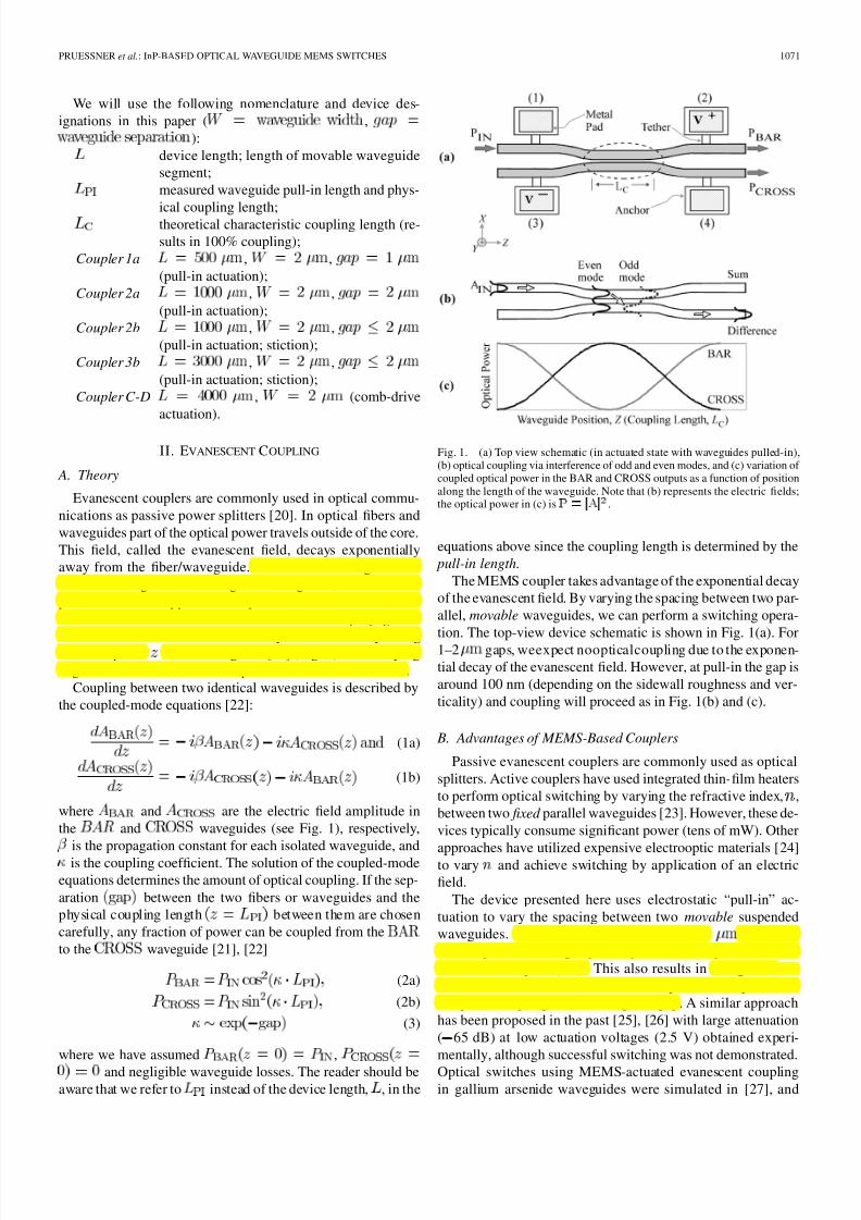
Fig. 1. (a) Top view schematic (in actuated state with waveguides pulled-in),(b) optical coupling via interference of odd and even modes, and (c) variation of coupled optical power in the BAR and CROSS outputs as a function of position
along the length of the waveguide. Note that (b) represents the electric fields;the optical power in (c) is
.
equations above since the coupling length is determined by the
pull-in length.
The MEMS coupler takes advantage of the exponential decay
of the evanescent field. By varying the spacing between two par-
allel, movable waveguides, we can perform a switching opera-
tion. The top-view device schematic is shown in Fig. 1(a). For
1–2 gaps, weexpect noopticalcoupling due to the exponen-
tial decay of the evanescent field. However, at pull-in the gap is
around 100 nm (depending on the sidewall roughness and ver-
ticality) and coupling will proceed as in Fig. 1(b) and (c).
B. Advantages of MEMS-Based Couplers
Passive evanescent couplers are commonly used as optical
splitters. Active couplers have used integrated thin-film heaters
to perform optical switching by varying the refractive index, ,
between two fixed parallel waveguides [23]. However, these de-
vices typically consume significant power (tens of mW). Other
approaches have utilized expensive electrooptic materials [24]to vary and achieve switching by application of an electric
field.
The device presented here uses electrostatic “pull-in” ac-
tuation to vary the spacing between two movable suspended
waveguides. The actuation distances are 1–2 , resulting
in low-power and high-speed operation (compared to elec-
trothermal couplers [23]). This also results in a large ON / OFF
contrast and low crosstalk due to the exponential dependence
of optical coupling on the waveguide gap. A similar approach
has been proposed in the past [25], [26] with large attenuation
( 65 dB) at low actuation voltages (2.5 V) obtained experi-
mentally, although successful switching was not demonstrated.
Optical switches using MEMS-actuated evanescent couplingin gallium arsenide waveguides were simulated in [27], and

8/11/2019 nova versão.pdf
http://slidepdf.com/reader/full/nova-versaopdf 3/12
8/11/2019 nova versão.pdf
http://slidepdf.com/reader/full/nova-versaopdf 4/12
PRUESSNER et al.: InP-BASED OPTICAL WAVEGUIDE MEMS SWITCHES 1073
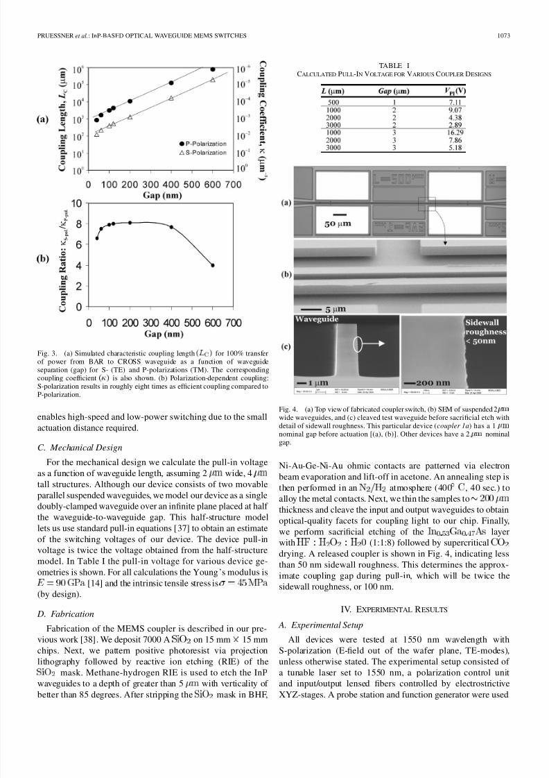
Fig. 3. (a) Simulated characteristic coupling length
for 100% transferof power from BAR to CROSS waveguide as a function of waveguideseparation (gap) for S- (TE) and P-polarizations (TM). The correspondingcoupling coef ficient
is also shown. (b) Polarization-dependent coupling:S-polarization results in roughly eight times as ef ficient coupling compared toP-polarization.
enables high-speed and low-power switching due to the small
actuation distance required.
C. Mechanical Design
For the mechanical design we calculate the pull-in voltage
as a function of waveguide length, assuming 2 wide, 4
tall structures. Although our device consists of two movable
parallel suspended waveguides, we model our device as a single
doubly-clamped waveguide over an infinite plane placed at half
the waveguide-to-waveguide gap. This half-structure model
lets us use standard pull-in equations [37] to obtain an estimate
of the switching voltages of our device. The device pull-in
voltage is twice the voltage obtained from the half-structure
model. In Table I the pull-in voltage for various device ge-
ometries is shown. For all calculations the Young’s modulus is
[14] and the intrinsic tensile stress is
(by design).
D. Fabrication
Fabrication of the MEMS coupler is described in our pre-
vious work [38]. We deposit 7000 A on 15 mm 15 mm
chips. Next, we pattern positive photoresist via projection
lithography followed by reactive ion etching (RIE) of the
mask. Methane-hydrogen RIE is used to etch the InP
waveguides to a depth of greater than 5 with verticality of better than 85 degrees. After stripping the mask in BHF,
TABLE ICALCULATED PULL-IN VOLTAGE FOR VARIOUS COUPLER DESIGNS
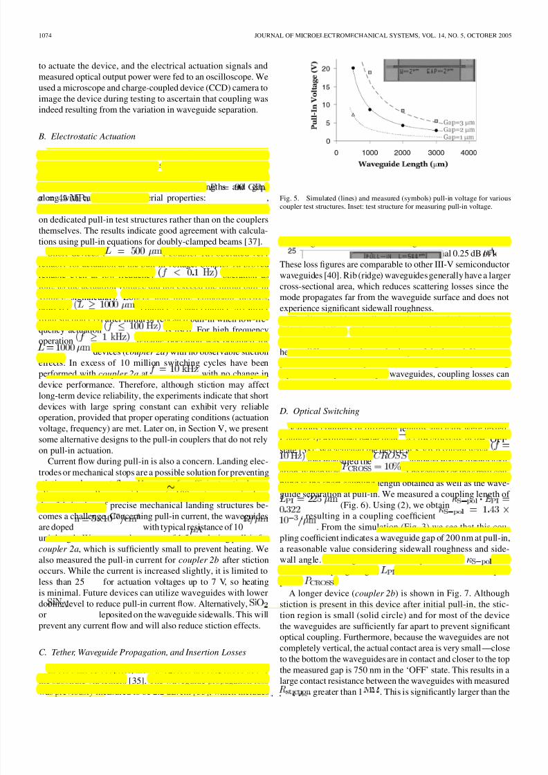
Fig. 4. (a) Top view of fabricated coupler switch, (b) SEM of suspended 2
wide waveguides, and (c) cleaved test waveguide before sacrificial etch withdetail of sidewall roughness. This particular device (coupler 1a) has a 1
nominal gap before actuation [(a), (b)]. Other devices have a 2 nominalgap.
Ni-Au-Ge-Ni-Au ohmic contacts are patterned via electron
beam evaporation and lift-off in acetone. An annealing step is
then performed in an atmosphere (400 , 40 sec.) to
alloy the metal contacts. Next, we thin the samples to
thickness and cleave the input and output waveguides to obtain
optical-quality facets for coupling light to our chip. Finally,
we perform sacrificial etching of the layer
with (1:1:8) followed by supercriticaldrying. A released coupler is shown in Fig. 4, indicating less
than 50 nm sidewall roughness. This determines the approx-
imate coupling gap during pull-in, which will be twice the
sidewall roughness, or 100 nm.
IV. EXPERIMENTAL RESULTS
A. Experimental Setup
All devices were tested at 1550 nm wavelength with
S-polarization (E-field out of the wafer plane, TE-modes),
unless otherwise stated. The experimental setup consisted of
a tunable laser set to 1550 nm, a polarization control unit
and input/output lensed fibers controlled by electrostrictiveXYZ-stages. A probe station and function generator were used
8/11/2019 nova versão.pdf
http://slidepdf.com/reader/full/nova-versaopdf 5/12
1074 JOURNAL OF MICROELECTROMECHANICAL SYSTEMS, VOL. 14, NO. 5, OCTOBER 2005
to actuate the device, and the electrical actuation signals and
measured optical output power were fed to an oscilloscope. We
used a microscope and charge-coupled device (CCD) camera to
image the device during testing to ascertain that coupling was
indeed resulting from the variation in waveguide separation.
B. Electrostatic Actuation
The present devices are electrostatically actuated—in con-
trast to our previously demonstrated devices, which were
electro-thermally actuated [38]. Fig. 5 shows the measured
pull-in voltage for various waveguide lengths and gaps
along with calculations (material properties: ,
intrinsic stress). Measurements were performed
on dedicated pull-in test structures rather than on the couplers
themselves. The results indicate good agreement with calcula-
tions using pull-in equations for doubly-clamped beams [37].
Short devices ( , coupler 1a) operated very
reliably for actuation at the pull-in voltage. Coupler 1a proved
reliable even at low-frequency operation as
long as the actuation voltage did not exceed the initial pull-in
voltage significantly. Longer and more compliant devices,
however, , coupler 2b and coupler 3b) suffer
from stiction [39] after initial or repeated pull-in when low-fre-
quency actuation is used. For high frequency
operation , reliable operation was obtained for
devices (coupler 2a) with no observable stiction
effects. In excess of 10 million switching cycles have been
performed with coupler 2a at with no change in
device performance. Therefore, although stiction may affect
long-term device reliability, the experiments indicate that short
devices with large spring constant can exhibit very reliableoperation, provided that proper operating conditions (actuation
voltage, frequency) are met. Later on, in Section V, we present
some alternative designs to the pull-in couplers that do not rely
on pull-in actuation.
Current flow during pull-in is also a concern. Landing elec-
trodes or mechanical stops are a possible solution for preventing
stiction and current flow. However, for ef ficient optical cou-
pling very small waveguide gaps ( 100 nm) are required, so
that fabrication of precise mechanical landing structures be-
comes a challenge. Concerning pull-in current, the waveguides
are doped with typical resistance of 10
unit length. We measured a current of 1.5 during pull-in for
coupler 2a, which is suf ficiently small to prevent heating. We
also measured the pull-in current for coupler 2b after stiction
occurs. While the current is increased slightly, it is limited to
less than 25 for actuation voltages up to 7 V, so heating
is minimal. Future devices can utilize waveguides with lower
doping level to reduce pull-in current flow. Alternatively,
or can be deposited on the waveguide sidewalls. This will
prevent any current flow and will also reduce stiction effects.
C. Tether, Waveguide Propagation, and Insertion Losses
In our MEMS couplers, the waveguides are suspended above
the substrate via tethers [35]. The waveguide propagation losswas previously measured to be 2.2 dB/cm [35], which includes
Fig. 5. Simulated (lines) and measured (symbols) pull-in voltage for variouscoupler test structures. Inset: test structure for measuring pull-in voltage.
scattering losses due to sidewall roughness as well as material
losses. Each tether pair introduces an additional 0.25 dB of loss.
These loss figures are comparable to other III-V semiconductor
waveguides [40]. Rib (ridge) waveguides generally have a larger
cross-sectional area, which reduces scattering losses since the
mode propagates far from the waveguide surface and does not
experience significant sidewall roughness.
The fiber-to-chip coupling loss dominates the insertion loss.
It is about 10 dB at the input and output of the coupler, resulting
in 20 dB total loss. Such losses are to be expected given the in-
herent differences in the mode-shape of the lensed fibers com-
pared to the mode-shape of the InP waveguides. By utilizing
tapers at the input and output waveguides, coupling losses can
be significantly reduced [41].
D. Optical Switching
Various couplers of different lengths and gaps were tested.
Coupler 1a exhibited better than 47 dB crosstalk in the ‘OFF’
state [38]. We actuated the device at 8 Vp-p square wave
and measured the coupled power during actu-
ation, w hich w as . T he r eason f or the s mall cou-
pling is the short coupling length obtained as well as the wave-
guide separation at pull-in. We measured a coupling length of
(Fig. 6). Using (2), we obtain
, resulting in a coupling coef ficient
. From the simulation (Fig. 3) we see that this cou-
pling coef ficient indicates a waveguide gap of 200 nm at pull-in,
a reasonable value considering sidewall roughness and side-
wall angle. For longer devices we expect similar , but
increased coupling length, , and hence increased coupled
power .
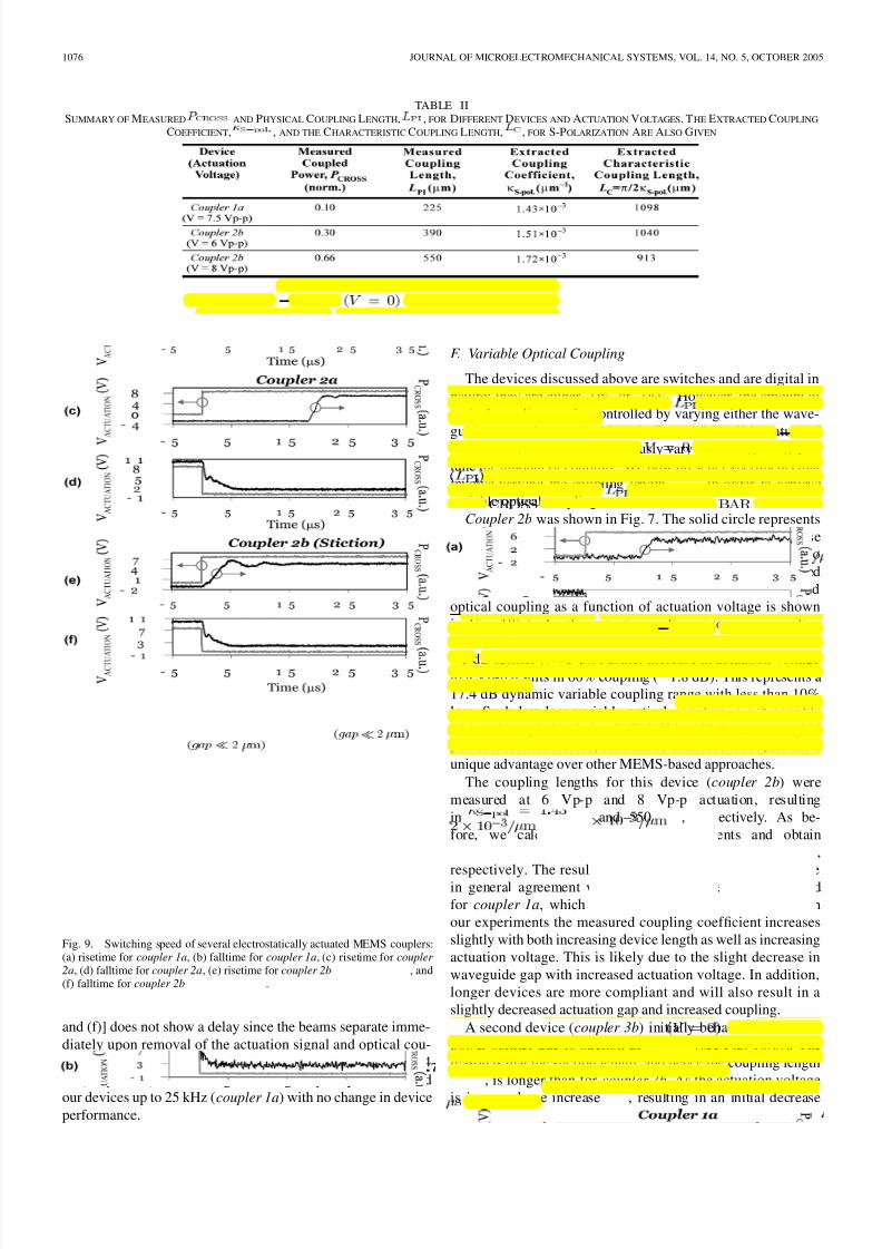
A longer device (coupler 2b) is shown in Fig. 7. Although
stiction is present in this device after initial pull-in, the stic-
tion region is small (solid circle) and for most of the device
the waveguides are suf ficiently far apart to prevent significant
optical coupling. Furthermore, because the waveguides are not
completely vertical, the actual contact area is very small—close
to the bottom the waveguides are in contact and closer to the top
the measured gap is 750 nm in the ‘OFF’ state. This results in a
large contact resistance between the waveguides with measuredgreater than 1 . This is significantly larger than the
8/11/2019 nova versão.pdf
http://slidepdf.com/reader/full/nova-versaopdf 6/12
PRUESSNER et al.: InP-BASED OPTICAL WAVEGUIDE MEMS SWITCHES 1075
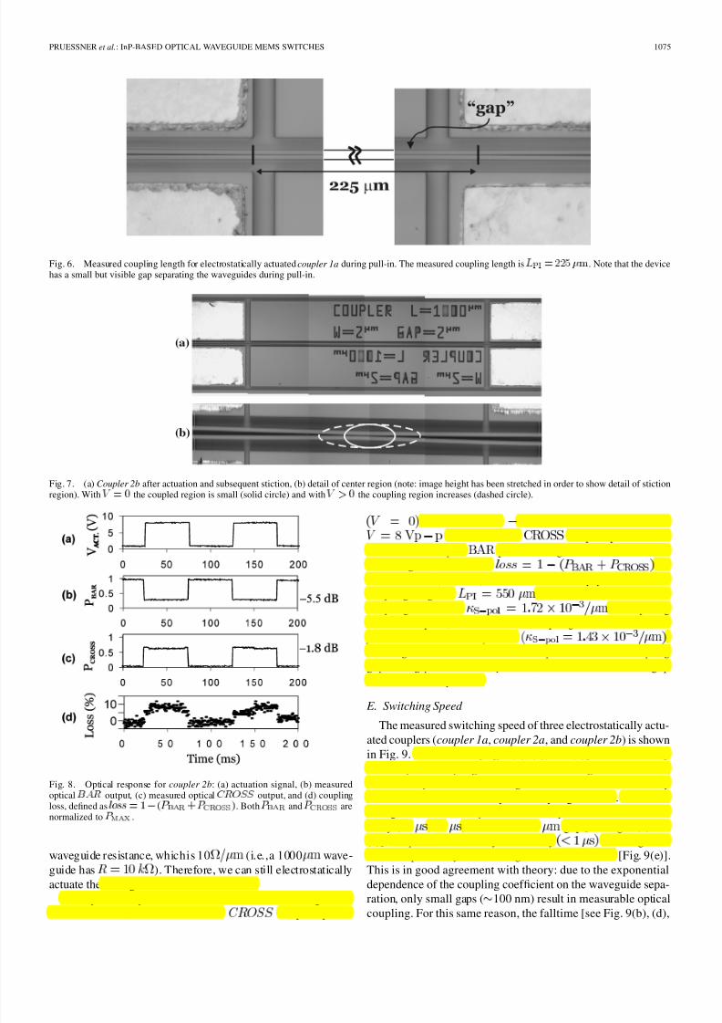
Fig. 6. Measured coupling length for electrostatically actuated coupler 1a during pull-in. The measured coupling length is
. Note that the devicehas a small but visible gap separating the waveguides during pull-in.
Fig. 7. (a) Coupler 2b after actuation and subsequent stiction, (b) detail of center region (note: image height has been stretched in order to show detail of stictionregion). With the coupled region is small (solid circle) and with the coupling region increases (dashed circle).
Fig. 8. Optical response for coupler 2b: (a) actuation signal, (b) measuredoptical
output, (c) measured optical
output, and (d) couplingloss, defined as
0
. Both
and
arenormalized to
.
waveguide resistance, whichis 10 (i.e.,a 1000 wave-
guide has ). Therefore, we can still electrostatically
actuate the waveguides in the stiction state.
The optical response of the device is shown in Fig. 8. Inthe “OFF” state, we measure 1.2% coupled power
. This results in 19.2 dB channel isolation. At
we obtain 66% coupled power and aminimum uncoupled power during actuation of 25%. The
switching loss, defined as , is
less than 10% (0.45 dB). For actuation at 8 Vp-p the measured
coupling length is , from which we obtain the
coupling coef ficient . Comparing
the two couplers, we find that the coupling coef ficient for cou-
pler 2b is similar to coupler 1a .
Looking at the simulations, we expect a 190 nm coupling
gap during pull-in for coupler 2b, similar to the 200 nm gap
obtained for coupler 1a.
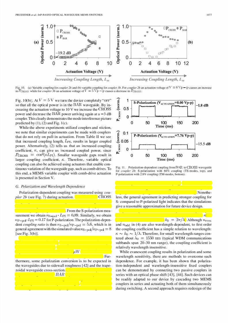
E. Switching Speed
The measured switching speed of three electrostatically actu-
ated couplers (coupler 1a, coupler 2a, and coupler 2b) is shown
in Fig. 9. The risetime [Fig. 9(a), (c), and (e)] exhibits a delay
before optical coupling occurs due to the waveguide travel time,
the time required for the waveguides to come into suf ficiently
close contact in order for optical coupling to occur. It is inter-
esting to note that coupler 1a and coupler 2a exhibit a clear
delay (10 , 18 ) due to the 1–2 gap [see Fig. 9(a) and
(c)]. Coupler 2b has a fairly small delay resulting from
the close proximity of the waveguides due to stiction [Fig. 9(e)].
This is in good agreement with theory: due to the exponential
dependence of the coupling coef ficient on the waveguide sepa-
ration, only small gaps ( 100 nm) result in measurable opticalcoupling. For this same reason, the falltime [see Fig. 9(b), (d),
8/11/2019 nova versão.pdf
http://slidepdf.com/reader/full/nova-versaopdf 7/12
1076 JOURNAL OF MICROELECTROMECHANICAL SYSTEMS, VOL. 14, NO. 5, OCTOBER 2005
TABLE IISUMMARY OF MEASURED
AND PHYSICAL COUPLING LENGTH,
, FOR DIFFERENT DEVICES AND ACTUATION VOLTAGES. T HE EXTRACTED COUPLING
COEFFICIENT,
, AND THE CHARACTERISTIC COUPLING LENGTH,
, FOR S-POLARIZATION ARE ALSO GIVEN
Fig. 9. Switching speed of several electrostatically actuated MEMS couplers:(a) risetime for coupler 1a, (b) falltime for coupler 1a, (c) risetime for coupler
2a, (d) falltime for coupler 2a, (e) risetime for coupler 2b
, and(f) falltime for coupler 2b
.
and (f)] does not show a delay since the beams separate imme-
diately upon removal of the actuation signal and optical cou-
pling decreases. The fastest switching speed we obtained was 4
(coupler 2b). Concerning switching frequency, we actuated
our devices up to 25 kHz (coupler 1a) with no change in deviceperformance.
F. Variable Optical Coupling
The devices discussed above are switches and are digital in
nature: they are either “ON” or “OFF.” However, the amount of
optical coupling can be controlled by varying either the wave-
guide gap or the coupling length. Due to the pull-in nature of our devices, we cannot continuously vary the waveguide gap to
tune the amount of coupling. We now present experiments that
involve varying the coupling length, , in order to achieve
variable optical coupling.
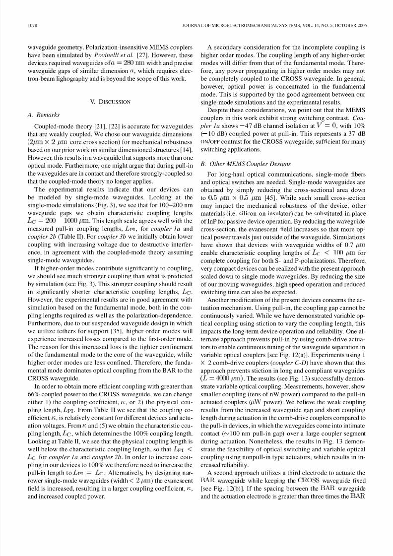
Coupler 2b was shown in Fig. 7. The solid circle represents
the coupling region in the rest state . As we increase
the actuation voltage, the coupling length increases as the two
waveguides come into contact over a larger length (dashed
circle), resulting in increased optical coupling. The measured
optical coupling as a function of actuation voltage is shown
in Fig. 10(a). As the actuation voltage increases, coupling
increases from 19.2 dB until the device acts as a
3 dB splitter (7 Vp-p). Further increase in actuation voltageto 8 Vp-p results in 66% coupling ( 1.8 dB). This represents a
17.4 dB dynamic variable coupling range with less than 10%
loss. Such low-loss variable optical coupling is not possible
with end-coupled switches [16]–[19] in which any uncoupled
power is lost. Therefore, our MEMS evanescent coupler has a
unique advantage over other MEMS-based approaches.
The coupling lengths for this device (coupler 2b) were
measured at 6 Vp-p and 8 Vp-p actuation, resulting
in and 550 , respectively. As be-
fore, we calculate the coupling coef ficients and obtain
and ,
respectively. The results are summarized in Table II and arein general agreement with the coupling coef ficient obtained
for coupler 1a, which had . In
our experiments the measured coupling coef ficient increases
slightly with both increasing device length as well as increasing
actuation voltage. This is likely due to the slight decrease in
waveguide gap with increased actuation voltage. In addition,
longer devices are more compliant and will also result in a
slightly decreased actuation gap and increased coupling.
A second device (coupler 3b) initially behaves as a 3 dB
power splitter due to stiction at [see Fig. 10(b)]. The
reason is that the stiction length, and hence the coupling length
, is longer than for coupler 2b. As the actuation voltage
is increased, we increase , resulting in an initial decreasein the power and an increase in the power [see
8/11/2019 nova versão.pdf
http://slidepdf.com/reader/full/nova-versaopdf 8/12
PRUESSNER et al.: InP-BASED OPTICAL WAVEGUIDE MEMS SWITCHES 1077
Fig. 10. (a) Variable coupling for coupler 2b and (b) variable coupling for coupler 3b. For coupler 2b an actuation voltage of 0
causes an increasein
while for coupler 3b an actuation voltage of 0
causes a decrease in
.
Fig. 10(b)]. At we turn the device completely “OFF”
so that all the optical power is in the waveguide. By in-
creasing the actuation voltage to 10 V we increase the
power and decrease the power arriving again at a 3 dBcoupler. This clearly demonstrates the mode interference picture
predicted by (1), (2) and Fig. 1(c).
While the above experiments utilized couplers and stiction,
we note that similar experiments can be made with couplers
that do not rely on pull-in actuation. From Table II we see
that increased coupling length, , results in larger coupled
power. Alternatively, (2) tells us that an increased coupling
coef ficient, , can give us increased coupled power, since
. Smaller waveguide gaps result in
larger coupling coef ficient, . Therefore, variable optical
coupling can also be achieved using actuators that enable con-
tinuous variation of the waveguide gap, such as comb-drives. Tothis end, a MEMS variable coupler with comb-drive actuation
is presented in Section V.
G. Polarization and Wavelength Dependence
Polarization-dependent coupling was measured using cou-
pler 2b (see Fig. 7) during actuation. The measured
coupled power for both S-and P-polarizations during actuation
is shown in Fig. 11. The results indicate 66% coupling for S-and
2.8% coupling for P-polarization. From the S-polarization mea-
surement we obtain . Similarly, we obtain
for P-polarization. The polarization-depen-
dent coupling ratio is then , which is ingeneral agreement with the simulated value
[see Fig. 3(b)].
Some of the discrepancy between simulation and experiment
is due to measurement error, taking into account scattered light
in our measurement setup. We note that the coupled power for
P-polarization is small (2.8%, or sub- levels) so that mea-
surement errors are increased compared to S-polarization. Fur-
thermore, some polarization conversion is to be expected in
the waveguides due to sidewall roughness [42] and the trape-
zoidal waveguide cross-section. Therefore, if we input 100%
P-polarized light into the input, then some portion will
be converted to S-polarized light resulting in increased cou-
pling compared to 100% P-polarized light. A third factor is thatthe waveguides are not strictly single-mode so that higher order
Fig. 11. Polarization-dependent coupling from
to
waveguide
for coupler 2b: S-polarization with 66% coupling (TE-modes, top), andP-polarization with 2.8% coupling (TM-modes, bottom).
modes may also contribute to the coupling. The simulations, in
contrast, assume single-mode waveguides and therefore predict
slightly lower coupling than we obtain experimentally. Nonethe-
less, the general agreement in predicting stronger coupling for
S- compared to P-polarized light indicates that the simulations
give a reasonable approximation for future device design.
Optical couplers also exhibit a slight wavelength-depen-
dence. From (4) we see that the coupling coef ficient, , is
proportional to the wavevector . Although
and in (4) are also wavelength-dependent, to first orderthe coupling coef ficient has a simple relation to wavelength:
. Therefore, for small wavelength ranges cen-
tered about (typical WDM communications
subbands span 20–30 nm range), the coupling coef ficient is
relatively wavelength insensitive.
While evanescent coupling results in polarization and some
wavelength sensitivity, there are methods to overcome such
dependence. For example, it has been shown that polariza-
tion-independent and wavelength-insensitive fixed couplers
can be demonstrated by connecting two passive couplers in
series with an optical phase shift [43], [44]. Such devices can
be readily adapted to our device by cascading two MEMS
couplers in series and actuating both of them simultaneouslyduring switching. A second approach requires redesign of the
8/11/2019 nova versão.pdf
http://slidepdf.com/reader/full/nova-versaopdf 9/12
1078 JOURNAL OF MICROELECTROMECHANICAL SYSTEMS, VOL. 14, NO. 5, OCTOBER 2005
waveguide geometry. Polarization-insensitive MEMS couplers
have been simulated by Povinelli et al. [27]. However, these
devices required waveguides of width and precise
waveguide gaps of similar dimension , which requires elec-
tron-beam lighography and is beyond the scope of this work.
V. DISCUSSION
A. Remarks
Coupled-mode theory [21], [22] is accurate for waveguides
that are weakly coupled. We chose our waveguide dimensions
core cross section) for mechanical robustness
based on our prior work on similar dimensioned structures [14].
However, this results in a waveguide that supports more than one
optical mode. Furthermore, one might argue that during pull-in
the waveguides are in contact and therefore strongly-coupled so
that the coupled-mode theory no longer applies.
The experimental results indicate that our devices can
be modeled by single-mode waveguides. Looking at the
single-mode simulations (Fig. 3), we see that for 100–200 nm
waveguide gaps we obtain characteristic coupling lengths
. This length scale agrees well with the
measured pull-in coupling lengths, , for coupler 1a and
coupler 2b (Table II). For coupler 3b we initially obtain lower
coupling with increasing voltage due to destructive interfer-
ence, in agreement with the coupled-mode theory assuming
single-mode waveguides.
If higher-order modes contribute significantly to coupling,
we should see much stronger coupling than what is predicted
by simulation (see Fig. 3). This stronger coupling should result
in significantly shorter characteristic coupling lengths, .However, the experimental results are in good agreement with
simulation based on the fundamental mode, both in the cou-
pling lengths required as well as the polarization-dependence.
Furthermore, due to our suspended waveguide design in which
we utilize tethers for support [35], higher order modes will
experience increased losses compared to the first-order mode.
The reason for this increased loss is the tighter confinement
of the fundamental mode to the core of the waveguide, while
higher order modes are less confined. Therefore, the funda-
mental mode dominates optical coupling from the BAR to the
CROSS waveguide.
In order to obtain more ef ficient coupling with greater than66% coupled power to the CROSS waveguide, we can change
either 1) the coupling coef ficient, , or 2) the physical cou-
pling length, . From Table II we see that the coupling co-
ef ficient, , is relatively constant for different devices and actu-
ation voltages. From and (5) we obtain the characteristic cou-
pling length, , which determines the 100% coupling length.
Looking at Table II, we see that the physical coupling length is
well below the characteristic coupling length, so that
for coupler 1a and coupler 2b. In order to increase cou-
pling in our devices to 100% we therefore need to increase the
pull-in length to . Alternatively, by designing nar-
rower single-mode waveguides (width ) the evanescent
field is increased, resulting in a larger coupling coef ficient, ,and increased coupled power.
A secondary consideration for the incomplete coupling is
higher order modes. The coupling length of any higher-order
modes will differ from that of the fundamental mode. There-
fore, any power propagating in higher order modes may not
be completely coupled to the CROSS waveguide. In general,
however, optical power is concentrated in the fundamental
mode. This is supported by the good agreement between oursingle-mode simulations and the experimental results.
Despite these considerations, we point out that the MEMS
couplers in this work exhibit strong switching contrast. Cou-
pler 1a shows 47 dB channel isolation at , with 10%
( 10 dB) coupled power at pull-in. This represents a 37 dB
ON / OFF contrast for the CROSS waveguide, suf ficient for many
switching applications.
B. Other MEMS Coupler Designs
For long-haul optical communications, single-mode fibers
and optical switches are needed. Single-mode waveguides are
obtained by simply reducing the cross-sectional area down
to [45]. While such small cross-section
may impact the mechanical robustness of the device, other
materials (i.e. silicon-on-insulator) can be substituted in place
of InP for passive device operation. By reducing the waveguide
cross-section, the evanescent field increases so that more op-
tical power travels just outside of the waveguide. Simulations
have shown that devices with waveguide widths of 0.7
enable characteristic coupling lengths of for
complete coupling for both S- and P-polarizations. Therefore,
very compact devices can be realized with the present approach
scaled down to single-mode waveguides. By reducing the size
of our moving waveguides, high speed operation and reduced
switching time can also be expected.Another modification of the present devices concerns the ac-
tuation mechanism. Using pull-in, the coupling gap cannot be
continuously varied. While we have demonstrated variable op-
tical coupling using stiction to vary the coupling length, this
impacts the long-term device operation and reliability. One al-
ternate approach prevents pull-in by using comb-drive actua-
tors to enable continuous tuning of the waveguide separation in
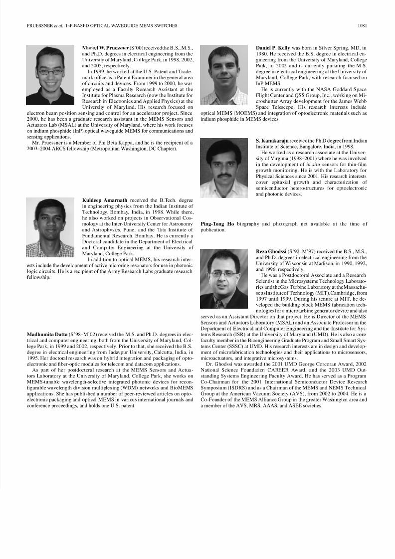
variable optical couplers [see Fig. 12(a)]. Experiments using 1
2 comb-drive couplers (coupler C-D) have shown that this
approach prevents stiction in long and compliant waveguides
. The results (see Fig. 13) successfully demon-
strate variable optical coupling. Measurements, however, showsmaller coupling (tens of nW power) compared to the pull-in
actuated couplers ( power). We believe the weak coupling
results from the increased waveguide gap and short coupling
length during actuation in the comb-drive couplers compared to
the pull-in devices, in which the waveguides come into intimate
contact ( 100 nm pull-in gap) over a large coupler segment
during actuation. Nonetheless, the results in Fig. 13 demon-
strate the feasibility of optical switching and variable optical
coupling using nonpull-in type actuators, which results in in-
creased reliability.
A second approach utilizes a third electrode to actuate the
waveguide while keeping the waveguide fixed
[see Fig. 12(b)]. If the spacing between the waveguideand the actuation electrode is greater than three times the
8/11/2019 nova versão.pdf
http://slidepdf.com/reader/full/nova-versaopdf 10/12
PRUESSNER et al.: InP-BASED OPTICAL WAVEGUIDE MEMS SWITCHES 1079
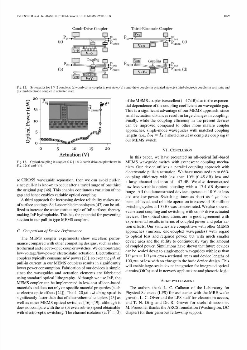
Fig. 12. Schematics for 1 2 2 couplers: (a) comb-drive coupler in rest state, (b) comb-drive coupler in actuated state, (c) third-electrode coupler in rest state, and(d) third-electrode coupler in actuated state.
Fig. 13. Optical coupling in coupler C-D [12
2 comb-drive coupler shown inFig. 12(a) and (b)].
to waveguide separation, then we can avoid pull-in
since pull-in is known to occur after a travel range of one thirdthe original gap [46]. This enables continuous variation of the
gap and hence enables variable optical coupling.
A third approach for increasing device reliability makes use
of surface coatings. Self-assembled monolayers [47] can be uti-
lized to increase the water contact angle of InP surfaces, thereby
making InP hydrophobic. This has the potential for preventing
stiction in our pull-in type MEMS couplers.
C. Comparison of Device Performance
The MEMS coupler experiments show excellent perfor-
mance compared with other competing designs, such as elec-trothermal and electro-optic coupler switches. We demonstrated
low-voltage/low-power electrostatic actuation. Electrothermal
couplers typically consume mW power [23], so even the of
pull-in current in our MEMS couplers results in significantly
lower power consumption. Fabrication of our devices is simple
since the waveguides and actuation elements are fabricated
using standard optical lithography. Although we use InP, the
MEMS coupler can be implemented in low-cost silicon-based
materials and does not rely on specific material properties (such
as electro-optic effects [24]). The 4–20 switching speed is
significantly faster than that of electrothermal couplers [23] as
well as other MEMS optical switches [16]–[19], although it
does not compare with the ns (or even sub-ns) speed obtainablewith electro-optic switching. The channel isolation (at )
of the MEMS coupler is excellent ( 47 dB) due to the exponen-
tial dependence of the coupling coef ficient on waveguide gap.
This is a significant advantage of our MEMS approach, since
small actuation distances result in large changes in coupling.
Finally, while the coupling ef ficiency in the present devices
can be improved compared to other more mature coupler
approaches, single-mode waveguides with matched coupling
lengths (i.e., ) should result in complete coupling in
our MEMS switch.
VI. CONCLUSION
In this paper, we have presented an all-optical InP-based
MEMS waveguide switch with evanescent coupling mecha-
nism. Our device utilizes a parallel coupling approach with
electrostatic pull-in actuation. We have measured up to 66%
coupling ef ficiency with less than 10% (0.45 dB) loss and
a large channel isolation of 47 dB. We also demonstrated
low-loss variable optical coupling with a 17.4 dB dynamic
range. All the demonstrated devices operate at 10 V or less
and are low-power. Switching times as short as 4 have
been achieved, and reliable operation in excess of 10 million
switching cycles at 10 kHz was demonstrated. We also showed
evanescent coupling and switching with comb-drive actuated
devices. The optical simulations are in good agreement with
experimental results in terms of coupled power and polariza-
tion effects. Our switches are competitive with other MEMS
approaches (mirrors, end-coupled waveguides) with regard
to optical loss and required power, but with much smaller
device area and the ability to continuously vary the amount
of coupled power. Simulations have shown that future devicescan be scaled down to single-mode waveguides with less than
cross-sectional areas and device lengths of
100 or less with no change in the basic device design. This
will enable large-scale device integration for integrated optical
circuits (OICs) used in network applications and photonic logic.
ACKNOWLEDGMENT
The authors thank L. C. Calhoun of the Laboratory for
Physical Sciences (LPS) for assistance with the MBE wafer
growth, L. C. Olver and the LPS staff for cleanroom access,
and T. N. Ding and Dr. R. Grover for useful discussions.
M. Pruessner thanks the ARCS foundation (Washington, DCchapter) for their generous fellowship support.

8/11/2019 nova versão.pdf
http://slidepdf.com/reader/full/nova-versaopdf 11/12
1080 JOURNAL OF MICROELECTROMECHANICAL SYSTEMS, VOL. 14, NO. 5, OCTOBER 2005
REFERENCES
[1] C. A. Brackett, “Dense wavelength division multiplexing networks:
principles and applications,” IEEE J. Sel. Areas Commun., vol. 8, pp.
948–964, 1990.
[2] E. Pennings, G. Khoe, M. K. Smit, and T. Staring, “Integrated-optic
versus microoptic devices for fiber-optic telecommunication systems:
a comparison,” IEEE J. Sel. Topics Quantum Electron., vol. 2, pp.
151–164, 1996.[3] H. Fujita and H. Toshiyoshi, “Optical MEMS,” IEICE Trans. Elec., vol.
E83, pp. 1427–1434, 2000.
[4] J. A. Walker, “The future of MEMS in telecommunications networks,” J. Micromech. Microeng., vol. 10, pp. R1–R7, 2000.
[5] S. Adachi, Physical Properties of III-V Semiconductor Com-
pounds. New York: Wiley, 1992.
[6] S. Greek, R. Gupta, and K. Hjort, “Mechanical considerations in thedesign of a micromechanical tuneable InP-based WDM filter,” J. Micro-
electromech. Syst., vol. 8, pp. 328–334, 1999.
[7] S. Irmer, J. Daleiden, V. Rangelov, C. Prott, F. Römer, M. Strassner, A.
Tarraf, and H. Hillmer, “Ultralow biased widely continuously tunable
Fabry-Pérot filter,” IEEE Photon. Technol. Lett., vol. 15, pp. 434–436,
2003.
[8] J. L. Leclercq,M. Garrigues, X. Letartre,C. Seassal, andP.Viktorovitch,
“InP-based MOEMS and related topics,” J. Micromech. Microeng., vol.
10, pp. 287–292, 2000.
[9] R. Ledantec, T. Benyattou, G. Guillot, C. Seassal, J. L. Leclercq,
X. Letartre, A. Gagnaire, M. Gendry, P. Viktorovitch, R. Benferhat,
D. Rondi, and R. Blondeau, “Optical characterization methods of
InP-based micro-opto-electro-mechanical systems,” SPIE , vol. 3008,pp. 258–264, 1997.
[10] R. Ledantec, T. Benyattou, G. Guillot, A. Spisser, C. Seassal, J. L.Leclercq, P. Viktorovitch, D. Rondi, and R. Blondeau, “Tunable micro-
cavity based on InP-air Bragg mirrors,” IEEE J. Sel. Topics Quantum
Electron., vol. 5, pp. 111–114, 1999.
[11] A. Spisser, R. Ledantec, C. Seassal, J.-L. Leclercq, T. Benyattou, D.
Rondi, R. Blondeau, G. Guillot, and P. Viktorovitch, “Highly selective
and widely tunable 1.55 um InP/air-gap micromachined Fabry-Perot
filter for optical communications,” IEEE Photon. Technol. Lett., vol. 10,
pp. 1259–1261, 1998.
[12] M. Strassner, J. Daleiden, N. Chitica, D. Keiper, D. Stalnacke, S. Greek,
and K. Hjort, “III-V semiconductor material for tunable Fabry-Perot fil-
ters for coarse and dense WDM systems,” Sensors and Actuators A, vol.A85, pp. 249–255, 2000.
[13] S. Greek,K. Hjort,J.-A.Schweitz,C. Seassal, J. L. Leclercq,M. Gendry,M. P. Besland, P. Viktorovitch, C. Figuet, V. Souliere, and Y. Monteil,
“The strength of indium phosphide based microstructures,” SPIE , vol.3008, pp. 251–257, 1997.
[14] M. W. Pruessner, T. King, D. Kelly, R. Grover, L. C. Calhoun, and
R. Ghodssi, “Mechanical property measurement of InP-based MEMS
for optical communications,” Sens. Actuators A, Phys., vol. A105, pp.
190–200, 2003.
[15] E. Gini and H. Melchior, “Thermal dependence of the refractive index
of InP measured with integrated optical demultiplexer,” J. Appl. Phys.,
vol. 79, pp. 4335–4337, 1996.
[16] E. Ollier, P. Labeye, and F. Revol, “Micro-opto mechanical switch inte-
grated on silicon,” Electron. Lett., vol. 31, pp. 2003–2005, 1995.
[17] E. Ollier, “Optical MEMS devices based on moving waveguides,” IEEE
J. Sel. Topics Quantum Electron., vol. 8, pp. 155–162, 2002.[18] T. Bakke, C. P. Tigges, J. J. Lean, C. T. Sullivan, and O. B. Spahn,
“Planar microoptomechanical waveguide switches,” IEEE J. Sel. Topics
Quantum Electron., vol. 8, pp. 64–72, 2002.[19] T. Bakke, C. P. Tigges, and C. T. Sullivan, “1
2
2 MOEMS switch based
on silicon-on-insulator and polymeric waveguides,” Electronics Letters,
vol. 38, pp. 177–178, 2002.[20] G. Keiser, Optical Fiber Communications, 3rd ed. Boston, MA: Mc-
Graw Hill, 2000.
[21] K. Okamoto, Fundamentals of Optical Waveguides. San Diego, CA:
Academic, 2000.
[22] R. G. Hunsperger, Integrated Optics: Theory and Technology, 5th
ed. Berlin, Germany: Springer, 2002.
[23] Q. Lai, W. Hunziker, and H. Melchior, “Low-power compact 22
2 ther-
mooptic silica-on-silicon waveguide switch with fast response,” IEEE
Photon. Technol. Lett., vol. 10, pp. 681–683, 1998.
[24] S. A. Samson, R. F. Tavlykaev, and R. V. Ramaswamy, “Two-section
reversed switch with uniform electrodes and domain reversal,” IEEE
Photon. Technol. Lett., vol. 9, pp. 197–199, 1997.
[25] F. Chollet, M. d. Labacherie, and H. Fujita, “Compactevanescent opticalswitch and attenuator with electromechanical actuation,” IEEE J. Sel.
Topics Quantum Electron., vol. 5, pp. 52–59, 1999.
[26] G. J. Veldhuis, T. Nauta, C. Gui, J. W. Berenschot, and P. V. Lambeck,
“Electrostatically actuated mechanooptical waveguide ON-OFF switch
showing high extinction at a low actuation-voltage,” IEEE J. Sel. Topics
Quantum Electron., vol. 5, pp. 60–66, 1999.
[27] M. L. Povinelli, R. E. Bryant, S. Assefa, S. G. Johnson, S. Fan, A. A. Er-
chak, G. S. Petrich, E. Lidorikis, J. D. Joannopoulos, L. A. Kolodziejski,andE. P. Ippen, “Design of a nanoelectromechanical high-index-contrast
guided-wave opticalswitch forsingle-mode operation at 1.55um,” IEEE
Photon. Technol. Lett., vol. 15, pp. 1207–1209, 2003.
[28] T. Oguchi, S. Tanaka, M. Hayase, and T. Hatsuzawa, “An electro-stat-
ically driven display device using evanescent coupling between a sheetwaveguide and multi-cantilevers,” Trans. Inst. Elec. Eng. Japan, vol.
124-E, pp. 87–92, 2004.[29] M.-C. M. Lee and M. C. Wu, “A MEMS-actuated tunable microdisk
resonator,” in Proc. IEEE/LEOS Conference on Optical MEMS , Hawaii,
2003, pp. 28–29.
[30] G. N. Nielson, D. Seneviratne, F. Lopez-Royo, P. T. Rakich, F. Gia-
cometti, H. L. Tuller, and G. Barbasthathis, “MEMS based wavelength
selective optical switching for integrated photonic circuits,” Conference
on Lasers and Electro-Optics, 2004.
[31] B. Broberg and S. Lindgren, “Refractive index of In(1-x)
Ga(x)As(y)P(1-y) layers and InP in the transparent wavelength region,” J. Appl. Phys., vol. 55, pp. 3376–3381, 1984.
[32] R. Grover, T. A. Ibrahim, S. Kanakaraju, L. Lucas, L. C. Calhoun, and
P.-T. Ho, “A tunable GaInAsP-InP optical microring notch filter,” IEEE
Photon. Technol. Lett., vol. 16, pp. 467–469, 2004.[33] S. S. Saini, F. G. Johnson, D. R. Stone, W. Zhou, H. Shen, and M. Da-
genais, “A 2 2 2 crosspoint switch fabricated on the passive active res-onant coupler (PARC) platform,” IEEE Photon. Technol. Lett., vol. 13,
pp. 203–205, 2001.
[34] C. L. Chang, S. Wagner, and A. A. Ballmann, “Optical absoprtion tail
in InP:Mn from surface photovoltage measurements,” Appl. Phys. Lett.,
vol. 43, pp. 1113–1115, 1983.
[35] D. Kelly, M. W. Pruessner, K. Amarnath, M. Datta, S. Kanakaraju, L. C.
Calhoun, and R. Ghodssi, “Monolithic suspended optical waveguides
for InP MEMS,” IEEE Photon. Technol. Lett., vol. 16, pp. 1298–1300,
2004.
[36] Optical Waveguide Mode Solver (OWMS): Version 1.21 ed., ApolloPho-
tonics, Waterloo, Canada, 1997–2001.[37] P. M. Osterberg and S. D. Senturia, “M-Test: a test chip for MEMS ma-
terial property measurement using electrostatically actuated test struc-tures,” J. Microelectromech. Syst., vol. 6, pp. 107–118, 1997.
[38] M. W. Pruessner, K. Amarnath, M. Datta, D. Kelly, K. Subramaniam,P.-T. Ho, and R. Ghodssi, “Optical and mechanical characterization of
an evanescent coupler optical switch,” in Proc. Solid-State Sensor, Ac-
tuator, and Microsystems Workshop, Hilton Head Island, SC, 2004, pp.
238–241.
[39] R. Maboudian and R. T. Howe, “Critical review: adhesion in surface mi-
cromechanical structures,” J. Vacuum Sci. Technol., vol. B15, pp. 1–20,
1997.
[40] R. J. Deri and E. Kapon, “Low-loss III-V semiconductor optical wave-
guides,” IEEE J. Quantum Electron., vol. 27, pp. 626–640, 1991.
[41] I. Moerman, P. P. Van Daele, and P. M. Demeester, “A review on fab-
rication technologies for the monolithic integration of tapers with III-V
semiconductor devices,” IEEE J. Sel. Topics Quantum Electron., vol. 3,pp. 1308–1320, 1997.
[42] E. M. Garmire and K. Honda, “Depolarization in channel glass waveg-
uides,” J. Lightw. Technol., vol. LT-4, pp. 220–227, 1986.[43] B. E. Little and T. Murphy, “Design rules for maximally flat wave-
length-insensitive optical power dividers using Mach-Zehnder struc-
tures,” IEEE Photon. Technol. Lett., vol. 9, pp. 1607–1609, 1997.
[44] T. E. Murphy, B. E. Little, and H. I. Smith, “Wavelength- and polariza-
tion-insensitive integrated directional couplers,” Integrated Photonics
Research Conference, 1999.
[45] R. Grover, T. A. Ibrahim, T. N. Ding, Y. Leng, L.-C. Kuo, S. Kanakaraju,
K. Amarnath, L. C. Calhoun, and P.-T. Ho, “Laterally coupledInP-based
single-mode microracetrack notch filter,” IEEE Photon. Technol. Lett.,
vol. 15, pp. 1082–1084, 2003.
[46] S. D. Senturia, Microsystem Design. Boston, MA: Kluwer Academic,
2000.
[47] H. Lim, C. Carraro, R. Maboudian, M. W. Pruessner, and R. Ghodssi,
“Chemical and thermal stability of alkanethiol and sulfur passivated
InP(100),” Langmuir , vol. 20, pp. 743–747, 2004.
8/11/2019 nova versão.pdf
http://slidepdf.com/reader/full/nova-versaopdf 12/12
PRUESSNER et al.: InP-BASED OPTICAL WAVEGUIDE MEMS SWITCHES 1081
Marcel W. Pruessner (S’00)receivedthe B.S., M.S.,and Ph.D. degrees in electrical engineering from theUniversity of Maryland, College Park, in 1998, 2002,and 2005, respectively.
In 1999, he worked at the U.S. Patent and Trade-mark of fice as a Patent Examiner in the general areaof circuits and devices. From 1999 to 2000, he wasemployed as a Faculty Research Assistant at the
Institute for Plasma Research (now the Institute forResearch in Electronics and Applied Physics) at theUniversity of Maryland. His research focused on
electron beam position sensing and control for an accelerator project. Since2000, he has been a graduate research assistant in the MEMS Sensors and
Actuators Lab (MSAL) at the University of Maryland, where his work focuseson indium phosphide (InP) optical waveguide MEMS for communications andsensing applications.
Mr. Pruessner is a Member of Phi Beta Kappa, and he is the recipient of a2003–2004 ARCS fellowship (Metropolitan Washington, DC Chapter).
Kuldeep Amarnath received the B.Tech. degreein engineering physics from the Indian Institute of Technology, Bombay, India, in 1998. While there,he also worked on projects in Observational Cos-mology at the Inter-University Center for Astronomyand Astrophysics, Pune, and the Tata Institute of
Fundamental Research, Bombay. He is currently aDoctoral candidate in the Department of Electricaland Computer Engineering at the University of
Maryland, College Park.In addition to optical MEMS, his research inter-
ests include the development of active microring resonators for use in photoniclogic circuits. He is a recipient of the Army Research Labs graduate researchfellowship.
Madhumita Datta (S’98–M’02) received the M.S. and Ph.D. degrees in elec-
trical and computer engineering, both from the University of Maryland, Col-lege Park, in 1999 and 2002, respectively. Prior to that, she received the B.S.degree in electrical engineering from Jadavpur University, Calcutta, India, in1995. Her doctoral research was on hybrid integration and packaging of opto-electronic and fiber-optic modules for telecom and datacom applications.
As part of her postdoctoral research at the MEMS Sensors and Actua-tors Laboratory at the University of Maryland, College Park, she works onMEMS-tunable wavelength-selective integrated photonic devices for recon-
figurable wavelength division multiplexing (WDM) networks and BioMEMS
applications. She has published a number of peer-reviewed articles on opto-electronic packaging and optical MEMS in various international journals and
conference proceedings, and holds one U.S. patent.
Daniel P. Kelly was born in Silver Spring, MD, in1980. He received the B.S. degree in electrical en-gineering from the University of Maryland, CollegePark, in 2002 and is currently pursuing the M.S.degree in electrical engineering at the University of Maryland, College Park, with research focused onInP MEMS.
He is currently with the NASA Goddard Space
Flight Center and QSS Group, Inc., working on Mi-croshutter Array development for the James WebbSpace Telescope. His research interests include
optical MEMS (MOEMS) and integration of optoelectronic materials such asindium phosphide in MEMS devices.
S. Kanakaraju receivedthe Ph.D degreefrom IndianInstitute of Science, Bangalore, India, in 1998.
He worked as a research associate at the Univer-sity of Virginia (1998–2001) where he was involved
in the development of in situ sensors for thin-filmgrowth monitoring. He is with the Laboratory for
Physical Sciences since 2001. His research interestscover epitaxial growth and characterization of semiconductor heterostructures for optoelectronic
and photonic devices.
Ping-Tong Ho biography and photograph not available at the time of publication.
Reza Ghodssi (S’92–M’97) received the B.S., M.S.,
and Ph.D. degrees in electrical engineering from theUniversity of Wisconsin at Madison, in 1990, 1992,and 1996, respectively.
He was a Postdoctoral Associate and a ResearchScientist in the Microsystems Technology Laborato-ries and theGas Turbine Laboratory at theMassachu-
settsInstituteof Technology (MIT),Cambridge, from1997 until 1999. During his tenure at MIT, he de-veloped the building block MEMS fabrication tech-nologies for a microturbine generator device and also
served as an Assistant Director on that project. He is Director of the MEMS
Sensors and Actuators Laboratory (MSAL) and an Associate Professor in theDepartment of Electrical and Computer Engineering and the Institute for Sys-tems Research (ISR) at the University of Maryland (UMD). He is also a core
faculty member in the Bioengineering Graduate Program and Small Smart Sys-tems Center (SSSC) at UMD. His research interests are in design and develop-ment of microfabrication technologies and their applications to microsensors,microactuators, and integrative microsystems.
Dr. Ghodssi was awarded the 2001 UMD George Corcoran Award, 2002National Science Foundation CAREER Award, and the 2003 UMD Out-standing Systems Engineering Faculty Award. He has served as a ProgramCo-Chairman for the 2001 International Semiconductor Device ResearchSymposium (ISDRS) and as a Chairman of the MEMS and NEMS Technical
Group at the American Vacuum Society (AVS), from 2002 to 2004. He is aCo-Founder of the MEMS Alliance Group in the greater Washington area and
a member of the AVS, MRS, AAAS, and ASEE societies.