novel devices circuits computing - university of california,...
TRANSCRIPT

Novel Devices and Circuits for Computing
UCSB 594BBWinter 2013
Lecture 4: Resistive switching: Logic

Class OutlineClass Outline
• Material Implication logicMaterial Implication logic
• Stochastic computing
fi bl l i• Reconfigurable logic

Material Implication Logic: Main IdeaMain Idea
Roff >> RGRon << RG

E i t lExperimental Demonstration

NAND via implication

Implication LogicPros• Inherently nonvolatile (intermittent power supply)• The finest grain pipeline (high throughput?)• Complicated peripheral circuitry
Cons:• Switch device with every logic operation
P h (1 J ti )• Power hungry (1 pJ per operation)
Feynman grand challengeNew ideas for processing in memory

Similar to Mat Imp Concepts but relying on Multistaterelying on Multistate
• Let’s do arithmetic operations by exploiting intermediate state, e.g.
A A B AA = A + B
A i t d t t
AS =
A is stored state B is coded to be proportional to pulse duration and/or pulse heightpulse height
Good or bad idea?Good or bad idea?


• Can also do division, multiplication• Base 512 was demonstrated

S h i C iStochastic Computing

Stochastic computing• Original idea due to John von Neumann in 1953• Represent numbers [0,1] as stream of random p [ , ]bits and reconstruct numbers by calculating frequencies
• Pa = ¾, Pb = ½ Pa*Pb = 3/8

Stochastic computing: Cons and Pros• PROS:
– Simple hardware for multiplication and additionR b t i t i– Robust against noise
– Provide rough estimate quickly with precision increasing with time
• CONS:– Exponential increase of
operation (or HW) with precisionprecision
• For N‐bit binary multiplication (2N‐bit product) needs 22Nsamples to have equivalent precision and, e.g. 24N samplesprecision and, e.g. 2 samples to have standard deviation of average frequency within the same precision
– Need random number generator


GOOD PROJECT/PAPER FOR RESEARCH!

Ideas for Memristor‐based Stochastic Computing?

R fi bl L iReconfigurable Logic

Island‐Type FPGAIsland Type FPGA
routing wires
clock
g
logic
block
logic
block
logic
block
flip
flop
LUTlogic
bl k
logic logic
bl k
three‐state
buffers
LUTblockblock block
memory bits Mux
logic
block
logic
block
logic
block

Example of Mapping 4‐bit Adder to 3‐LUTs
c0=0
full adders0a0
b0cin
a b cin
input outputc1
full adders1a1
b1c2
full adders2a2
sa
b 1
1
0
1
0
s
0
0
1
0
0
cout
LLa b cin sum cout
0 0 0 0 0
1 0 0 1 0
0 1 0 1 0
1 1 0 0 1s2 b2
c3
full adders3a3
b3
C4
cout
0
0
1
1
1
17 7
0 0 1 1 0
1 0 1 0 1
0 1 1 0 1
1 1 1 1 1
Ripple carry adder Truth table Full adder circuit LUT implementation

Example of Mapping to FPGAExample of Mapping to FPGAc0
s0
1 0
a0
b0
1 000
1 0
0 0 0 0
b0
0110 1
La0 00010
01 1
0
a0
b0
L
10017
11
s1
1 0 0 0
011
0
a
01117
c0 c0
c1
0 1 0 0
s1
1 0 01
a1
b1

Cons and Pros of FPGAs• Circuitry is customized for a particular
i ( i lcomputation (massively parallel, bit‐granularity)
• Long configuration time g g– good for repetitive or slowly changing computations p
• Not as transparent for programmer and easy as uP andas uP and
• Very high overhead for reconfigurability …

Dominant Area and Power
Mingijie Lin, El Gamal, Simon Wong,IEEE Tran CAD, 26(2), pp. 216, 2007( ) pp
5%
21%
9% 5%
InterconnectClockIO
XC4003A data from Eric Kusse (UCB MS 1997)
65% CLBMS 1997)

Hybrid CMOS/Memristor FPGA: Main IdeaMain Idea
typical FPGA … … and with lifted config. bits
metallizationmetallization& config. bits
config. bits & logic logic
& config. bits
~ 90% is interconnect (memory bits +
three state buffers/pass gates)
Crosspoint memristivedevice somewhere in the
layer above CMOSp g )
Density, speed, power improvement configurable ASIC

Hybrid CMOS‐Memristor FPGA: First DemoDemo (c) (d) (a)
n anowire layer 2
(titanium) NOT gate
nanowire layer 1
m emristive layer
AND gate
NOT gate
CMOS layer
aye (platinum)
NOT t NAND gate
OR gate
(b )
AND gate
NOT gate
NAND gate
NOR gate
NAND gate
OR t
D flip flop
Q. Xia et al. NanoLetters, 2009
gate
NOR gate
D flip flop 10x improvement in density (theoretical) as compared to pure CMOS with comparable power and latency


CMOL FPGA
‐ Use memristors not only as interconnect but also to implement part of functionality‐ Analog properties of memristors to implement linear threshold gates
Generic CMOL FPGA
BA+B
cell AB F
A B
Linear Threshold Logic
CMOS fl fl
x1 x2 x3 x4
A
nanodevices
A+B
A
RON
B
R
VOUTPUT
D flip‐flop
N
RONV0
CMOS inverterA+B
RpassCwireRL
Memristors logic and routingL. Gao Trans. Nanotechnology 2013
Strukov and Likharev, Nanotechnology, 2005

Open Research Problems with f blReconfigurable Logic
1) The lower the resistance the more overhead for CMOS1) The lower the resistance the more overhead for CMOS programming circuitry what is the optimum?
2) Wh i h l i l f h i h2) When switches are relatively free what is the new optimum architecture for switch box/interconnect/logic?

Choices for Interconnect TopologyBUS CROSSBAR
• Flexibility (+)– routes
hi ( i• Flexibility (++)
routes
BUS vs CROSSBAR
everything (given enough time)
– can be tricky to schedule use
– routes everything (guaranteed)
• Delay (Power) (‐)optimally
• Delay (Power) (‐‐)– wire length O(kn)
– wire length O(kn)
– parasitic stubs: kn+n
– parasitic stubs: kn+n
– series switch: 1O(kn)
– series switch: 1– O(kn)
• Area (‐)– O(kn)– sequentialize I/B
• Area (++)kn switches
– Bisection bandwidth n
– kn2 switches– O(n2)– kn switches
– O(n)O(n )

Exploit Locality: Rent’s RuleExploit Locality: Rent s Rule
• In the world of circuit design, an empiricalIn the world of circuit design, an empirical relationship to capture:
IO = c NpIO = c Np
• 0p1p• p – characterizes interconnect richness• Typical: 0 5p0 7Typical: 0.5p0.7• “High‐Speed” Logic p=0.67

Rent and LocalityRent and Locality
• Rent and IO capture/quantifying localityRent and IO capture/quantifying locality– local consumption
local fanout– local fanout
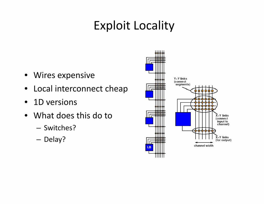
Exploit Locality
• Wires expensive
• Local interconnect cheap• Local interconnect cheap
• 1D versions
• What does this do to• What does this do to – Switches?
– Delay?Delay?

Exploit Locality
• Wires expensive
• Local interconnect cheap
• Use 2D to make more things closer
• Mesh?

Mesh Analysis
• Flexibility ‐ ?Ok w/ large w
• AreaBisection BW wn– Ok w/ large w
• Delay (Power)– Series switches
– Bisection BW ‐‐ wn– Switches ‐‐ O(nw)
– O(w2n) Series switches• 1‐‐n
– Wire length
( )
n blocks
• w‐‐wn
– Stubs• O(w) O(wn)
w
• O(w)‐‐O(wn)
Assuming that BW scales as NP (from Rent Rule)
N p
NNW
p5.0
For large N always wire limited!