nuclear battery olsen
TRANSCRIPT
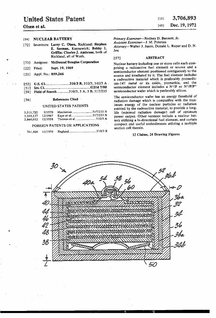
United Statesv Patent [15] 3,766,893 Olsen et a1. 1451 Dec. 19, 1972
1541 NUCLEAR BATTERY Primary Examiner-Rodney D. Bennett, Jr. [72] Inventors: Larry C. Olsen, Richland; Stephen Asmtam Exammer *1 ' M‘ Potenzia
E. Seeman, Kennewick; Bobby I. Griffin; Charles J. Ambrose, both of Richland, all of Wash.
[73] Assignee: McDonnel Douglas Corporation
[22] Filed: Sept. 19, 1969
[21] Appl. No.: 859,266
[52] *U.S. Cl.’ ................ ..'......310/3 B, 3l0/3,.310/3 A. [51] lint. Cl. ............................................. ..G2ld 7/00 [58] Field of Search .......... ..3lO/3, 3 A, 3 B; 317/235
[56] References Cited '
UNITED STATES PATENTS
3,511,722 5/1970 ’ Meuleman ...................... .;317/235 N
3,359,137 12/1967 Kaye et a1 ........ .. ....3l7/235 N 2,864,012 12/1958 Thomas et a1. ..................... ..3l0/3 A
FORElGN PATENTS OR APPLICATIONS
761,404 11/1956 England .............................. “310/3 13
Attorney-Walter J. Jason, Donald L. Royer and D. N. Jeu
[5 7 ] ABSTRACT
Nuclear battery including one or more cells each com prising a radioactive fuel element or source and a semiconductor element positioned contiguously to the source and irradiated by it. The fuel element includes a radioactive material which is preferably promethi um-147 metal or its. oxide, promethia, and the W, semiconductor element includes a N+/P or N‘llli'll’+ semiconductor wafer which is preferably silicon.
The semiconductor wafer has an energy threshold of radiation damage which is compatible with the max imum energy of the nuclear particles or radiation emitted by the radioactive material, to provide a long life (minimal radiation damage) cell of optimum power output. Other versions include a nuclear bat tery utilizing a bi-directional fuel element, and certain compact and useful embodiments utilizing a multiple section cell therein.
12 Claims, 24 Drawing Figures
/ ‘V 40y}, . . . . 52'
4% V/\\ \ ? // ' \ \ \ \ \ \ \
.\\\,\\\\\\\\:\\\\\\\\\\ 5 2% ~ 1%
a5 a?‘ 2. 54% //
50
3,706,893 I
NUCLEAR BATTERY
BACKGROUND OF THE INVENTION
Our present invention pertains generally to the ?eld of batteries and more particularly to a nuclear battery wherein nuclear energy is usefully converted into elec trical energy.
Generally, prior radioactive or nuclear batteries which involve the concept of coupling a radioactive source with one or more semiconductor elements have utilized a source of high energy radiation to irradiate the semiconductor elements that each include a NP junction therein. The radiation damage created by the high energy particles or radiation in these prior batte ries is so great, however, that their useful lifetimes are so short as to render such batteries to be of questiona ble value.
Further, the power density, maximum output power, maximum output voltage and device efficiencies are relatively quite low for the prior radioactive or nuclear batteries. The various known concepts of radioactive or nuclear batteries do not in most instances appear to be particularly feasible, and all of such concepts are either clearly impractical or are of little useful value. It is, of course, well known that a general purpose nuclear battery other than this invention and of a similar category is not presently and readily available on the commercial market.
SUMMARY OF THE INVENTION
Brie?y, and in general terms, ‘ our invention is preferably accomplished by providing a nuclear battery including one or more cells each comprising a radioac tive fuel element or source and a semiconductor ele ment positioned in close proximity or contiguously to the source and irradiated by it. The semiconductor element is made of a material
which has an energy threshold level of radiation damage that is compatible with the maximum energy of the nuclear particles or radiation emitted by the radioactive source. The fuel element includes a radioactive material which is preferably promethium 147 (Pm‘‘") metal or its oxide, promethia (Pm,o,), and the semiconductor element includes a N+/P or N+/P/P“ semiconductor wafer which is preferably silicon (Si), to provide a long-life (minimal radiation damage) cell of optimum power output. The semiconductor wafer is preferably characterized by having at least a N*~type layer which has a very high density of conduction elec trons. In the three-layer semiconductor wafer, the I“ type layer has a very high density of “holes," of course. In both instances (N? or I“), the carrier density preferably approaches 102° or 1021 carriers/cm3 in order that maximum voltage be obtained. The radioactive fuel element and the semiconductor
element of a cell are preferably discs of similar sizes. The fuel element is also preferably positioned virtually against the N+-type layer surface of the semiconductor wafer. The N"/lD and N‘VlP/ll”r (silicon) semiconductor wafers are preferred because they are more resistant to damage caused by (beta) radiation. However, PIN and WIN/N+ semiconductors (N-type semiconductor stock) can, of course, be used satisfactorily in this in vention.
In the NH]? semiconductor wafer, the highly doped N+-type layer face thereof provides a large number of
7653
30
35
45
55
60
65
2 conduction electrons which are available to an external circuit or load. In the N+IPIP+ semiconductor wafer, both faces thereof are highly doped to have high carrier concentrations such that the resulting N*-type layer and P*-type layer faces prevent any bending of the electron bands in the wrong sense and thus generate an electromotive force of the incorrect polarity. These highly doped surfaces essentially “lock" the electron bands in place whereby the semiconductor surfaces can be treated in any manner desired without degrading device performance. In such an arrangement, ohmic contacts can be easily made to the semiconductor faces and, in fact, any adjacent oxide layers formed thereon will not alter the electron band structure to affect the performance of the device. The resulting nuclear batte ries can be manufactured with power levels covering a wide range and have long lifetimes (of over three years) with high power densities (of one milliwatt/cm3 or more).
Other versions of our invention include a two-cell nuclear battery utilizing a bi-directional fuel element or source, a planar multiple section cell nuclear battery embodiment, a laminar multiple section cell nuclear battery con?guration and an elongated, cylindrical multiple section cell nuclear battery embodiment. The nuclear battery configurations including a multiple sec tion cell therein are particularly compact and practical forms of our invention, and can supply electrical power at voltages much greater than that available from an equivalent single cell which utilizes only one active area.
BRIEF DESCRIPTION OF THE DRAWINGS
Our invention will be more fully understood, and other features and advantages thereof will become ap parent, from the following description of certain illus trative embodiments of the invention. The description is to be taken in conjunction with the accompanying drawings, in which:
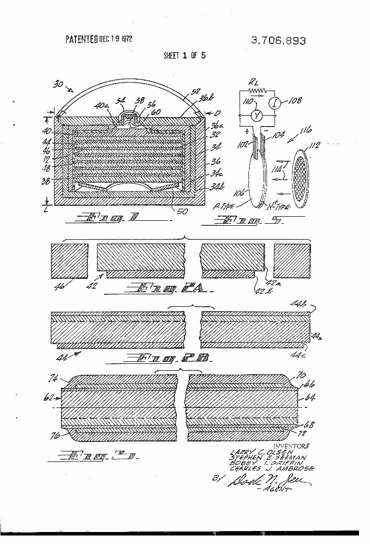
FIG. 1 is a central sectional and elevational view, perspectively shown, of a nuclear battery constructed in accordance with our invention;
FIGS. 2A and 2B are enlarged fragmentary and cen tral sectional views of a fuel element and its concentric ring, and a semiconductor element, respectively, of the nuclear battery shown in FIG. 1;
FIG. 3 is an enlarged fragmentary and central sec tional view of a directly fueled nuclear battery cell;
FIG. 4 is an electron energy level diagram for a N‘VP/P‘r semiconductor device;
FIG. 5 is a circuit diagram showing a resistive load connected to positive and negative electrodes of a N+/P semiconductor device;
FIG. 6 is a circuit diagram of an equivalent circuit of the semiconductor device shown in FIG. 5 connected to its resistive load;
FIG. 7 is a graph illustrating current density and power density versus output voltage characteristics of a single cell device constructed according to this inven tion;
FIGS. 8A, 8B, 8C and 8D are graphs which were plotted from experimental results and show typical characteristics of promethia-fueled, silicon semicon ductor, betavoltaic single cells as a function of promethia layer thickness;
l060ll 0590

3,706,893 3
FIGS. 9A and 9B are respectively a perspective view of a bi-directional fuel element or source, and a frag mentary and enlarged sectional view thereof;
FIGS. 10A and 10B are exploded perspective views of a two-cellbetavoltaic energy converter or battery using the bi-directional source of FIG. 9A, wherein the cells are connected respectively in parallel and in se ries;
FIG. 11 is an elevational view of a N+/P semiconduc tor wafer having a promethium coating deposited directly onto the N+-type layer surface of the wafer;
FIG. 12 is an exploded perspective view of a two-cell betavoltaic battery having a radioactive material coated directly on at least one semiconductor wafer of the cells;
FIG. 13 is an exploded perspective view of a highly compact and practical form of a nuclear battery con structed according to this invention; -
FIG. 14 is'a graph illustrating the current and power versus voltage characteristics of a nuclear battery such as that shown in FIG. 13;
FIG. 15 is an exploded perspective view of a planar, multiple section, cell embodiment of a nuclear battery;
FIG. 16 is a partially fragmentary and exploded‘ per spective view of a laminar, multiple section, cell con ?guration of a nuclear battery; ‘
FIG. 17 is an electron energy level diagram for about two sections of the N+/P+/P semiconductor device shown in FIG. 15; and
FIG. 18 is an exploded and partly fragmentary per spective view of an elongated cylindrical, multiple sec tion, cell embodiment of a nuclear battery.
DESCRIPTION OF THE PRESENT EMBODIMENTS
FIG. I is a central sectional and elevational view, perspectively shown, of a nuclear battery 30 con structed in accordance with our invention. The battery 30 broadly includes a radioactive fuel-semiconductor stack 32, and inner and outer containers 34 and 36 for suitably enclosing and housing the stack. The stack 32 includes lower and upper metallic discs 38 and 40 which sandwich a number of radioactive fuel elements 42 and semiconductor elements 44 that are con tiguously positioned in alternate layers. The diameter of the fuel elements 42 is smaller than that of the semiconductor elements 44, such that metallic rings 46 having an inner diameter larger than that of the fuel elements and an outer diameter equal to that of the semiconductor elements, can be positioned concentri cally around and radially spaced from the semiconduc tor elements in the same corresponding layers thereof. The lower metallic disc 38 is in direct contact with
the lower fuel element 42 and its concentric metallic ring Q6. The upper metallic disc 1&0 is in direct contact with the upper ‘semiconductor element 44. An insulat ing liner 48 made of radiation resistant rubber or an ox ide, for example, is provided'around the sides or cir cumferential surface of the stack 32 and over the upper surface of the metallic disc 60 except for a central area 40a thereof, as shown in FIG. 1. The liner 45 insulates the stack 32 from the inner sleeve 34a of inner con tainer 34 which can be fabricated of tantalum (Ta), for example. The inner container 3t includes an outer sleeve 34b which is closed at its lower end to support the stack 32 through a metallic spring ring 50. The
7654
15
20
25
30
35
40
45
55
60
65
4 spring ring 50 also provides an electrical connection between the lower disc 38 and the inner container 34. The inner container 34 is enclosed by and in direct.
contact with the outer container 36 which is preferably a closed stainless steel ?re can. The outer container 36 includes a lower can portion 36a and an upper cover portion 36b which can be electron beam welded to the can portion at the juncture 52 thereof. The cover por tion 36b has a central and countersunk hole 54 therein. A small insulating sleeve 56 of ceramic or glass, for ex ample, is positioned within the countersunk portion of the hole 54 and supports a closing metallic 'disc'58 which is electrically connected‘ by lead 60 to the central area 40a of the upper metallic disc 40. Glass-to-metal seals are, of course, suitably provided at the lower and upper ends of the insulating sleeve 56. Thus, the disc 58 is one (positive) electrode andthe outer container 36 is the other (negative) electrode of the nuclear battery 30. The battery 30 as shown illustratively in FIG. l is cylindrical in con?guration; however, it obviously can be made in rectangularor other con?gurations. The battery 30 has outside or overall dimensions of diame ter D and length L.‘ -
FIGS. 2A and 2B are enlarged fragmentary and cen tral sectional views of a fuel element 42 and its concen tric ring 46, and a semiconductor element .434, respec tively. In FIG. 2A, the ring 46 can be made of alu minum (Al) and can have an outer diameter of approx imately 1 cm, for example. The fuel element 42 in cludes an aluminum disc 42a and a thin layer 4212 of promethia (PmgOa) thereon. The ring so can have an inner diameter of approximately 0.95 cm, and the disc 42a can have a diameter of approximately 0.93 cm and a thickness typically of from 3 tov 10 mils. This thickness is primarily for strength andhandling. Nickel (Ni) or tantalum, for example, can be used instead of aluminum. The disc 42a is preferably sand-blasted on a face ?rst and then the promethia layer 42b can be pro vided tenaciously thereon by vapor deposition. The promethia layer 42b can be provided on the face with a layer thickness of approximately 5.3 milligram/cm2, for example. Promethia is preferably used since it is a good and stable source ofbeta particles or radiation. It is, of course, to be understood that the various types of materials. and different dimensions noted herein are given by way of example only and are not intended to be restrictive or limiting on the scope of our invention in any manner.
In FIG. 2B, the semiconductor element 414 has an outer diameter which 'is preferably equal to the outer diameter of the ring 46 (FIG. 2A). The semiconductor element 44 includes a N+/P silicon (Si) wafer Me, a thin metallic upper layer 44b and a thin metallic lower layer 44c. The wafer 44a can have a thickness of from 3 to 15 mils, for example. This wafer ‘Ma can be, if desired, a N+/P/P+ silicon wafer in accordance with this invention. The upper and lower layers 44b and Me can be of aluminum, and the upper layer 44b provides an electrical ohmic contact from the Nttype surface of wafer 44a to the lower surface of (an upper) ring 46 while the lower layer 44c provides an electrical ohmic contact from the P-type surface of wafer 44a to the upper surface of (a lower) ring 46 and, incidentally, to the upper surface of (a lower) disc 42a. The upper layer 44b is, of course, sufficiently thin (less than 2
106011 059i
3,706,893 5
microns thick, for example) to permit adequate penetration thereof by the beta radiation from the con tiguous promethia layer 42b above it. in one particular embodiment, the upper layer 44!; is actually in the form of a grid (generally similar to a wire screen) wherein each mesh or enclosed space allows free passage of the beta particles or radiation therethrough. The upper and lower layers 44b and 460 can be of silver (Ag) instead of aluminum, and are preferably vapor deposited or plated on the wafer 454a. The lower layer 44c can be 1 mil thick although 2 microns would be adequate. The thin metallic layer and grid are both distributed
or extended electrode forms which provide good ohmic contact with the full lower and upper surfaces of the semiconductor wafer 44a. A grid providing an ohmic contact to a given semiconductor surface (unit reference) area has a certain fractional ohmic contact area and a remaining fractional open area for passage of beta particles or other radiation. A thin metallic layer obviously provides maximum (lowest resistance) contact over the full semiconductor surface with, how ever, a zero fractional open area for free passage of the beta particles or radiation. Of course, the distributed ohmic contact area of a grid or any other such ex tended electrode form with a given semiconductor sur face area must be adequate to achieve a suitable balance between the fractional open area obtainable for free passage of the beta particles or radiation com mensurate with maintaining a sufficiently extensive and good (low resistance) ohmic contact for the entire semiconductor surface area. In this respect, a minimum distributed ohmic contact area is required with a highly conductive (high carrier concentration) semiconduc tor surface.
in our invention, beta radiation is preferably coupled with either a NV? or N"/l:’/P‘r silicon wafer. The N+/P silicon wafer is a two-layer silicon system including a N’r-type layer characterized by a phosphorus (P) con centration of approximately 10‘9 to 102° atoms/cm.3 and a P-type layer characterized by a boron (B) concentra tion of approximately 1016 atoms/cm3 (or a P-type layer having a resistivity of approximately 1 ohm-cm). The NHP/l“ silicon wafer can be produced from a N+/P sil icon wafer by diffusing a suitable amount of boron into the lower surface of the lP-type layer or region of the sil icon wafer to produce a P+-type layer therein. The N?'P/P’r silicon wafer is a three~layer silicon system in cluding N+-type and P-type layers as in the above N+IP silicon wafer, and a Pf-type layer characterized by a boron concentration of approximately 10‘9 to 102° atoms/cm? In both of these types of silicon wafers, ar senic (As), antimony (Sb) or bismuth (Bi) can be sub stituted for phosphorus, and aluminum, gallium (Ga), indium (in) or thallium (Tl) can be substituted for boron. Germanium (Ge), cadmium sulfide (CdS) and gallium arsenide (GaAs) semiconductors, among others, can be used instead of silicon. However, more power can be obtained from silicon cells than from the others. For example, roughly ?ve times more power can be usually derived from a silicon cell than from a generally similar germanium cell.
FIG. 3 is an enlarged fragmentary and central sec tional view of a directly fueled nuclear battery cell 62. A N+/1P (or N*/P/P+) semiconductor wafer 66 of sil icon, for example, has both upper and lower surfaces
7655
20
25
30
35
40
45
50
55
60
65
6 coated with thin metallic layers 66 and 68, respectively, which can be of aluminum, nickel or silver. Suitably deposited thereon are respective layers 70 and 72 of a source of beta radiation material such as promethia or promethium-l47 (Pmm) metal. The radioactive layers 70 and 72 are smaller in diameter than that of the semiconductor wafer 64, as illustrated. The radioactive layers 70 and 72 are then fully covered by outer metal lic layers 74 and 76, respectively, which can be of alu minum or silver and are for electrical contact. The radially outer circumferential (lower) surface
portion of the upper cover layer 74 contacts the cor responding portion of the thin metallic layer 66 which is in contact with the surface of the P-type layer of the semiconductor wafer 64. Similarly, the radially outer circumferential (upper) surface portion of the lower cover layer 76 contacts the corresponding portion of the thin metallic layer 68 which is in contact with the surface of the N+-type layer of the wafer 64. Thus, the upper cover layer 74 is of positive polarity and the lower cover layer 76 is of negative polarity for the bat tery cell element 62. The cell elements 62 can be readi ly stacked in series for a higher output voltage and, of course, the stacks can also be suitably connected in parallel as may be desired or required.
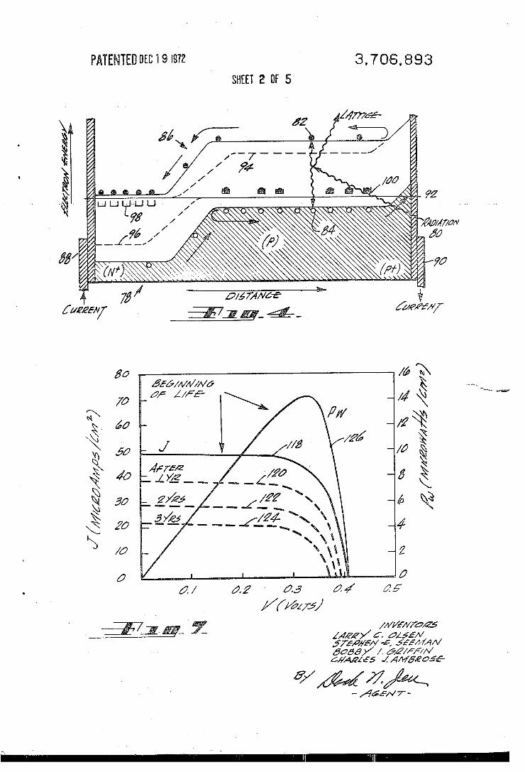
FIG. 4 is an, electron energy level diagram for a N‘VP/P+ semiconductor wafer 78. Nuclear-voltaic ef fects are initiated when radiation 80 enters the semiconductor 78 and creates electron 82 and hole 84 pairs. A large number of these carriers (electrons and holes) diffuse to the vicinity of the abrupt (N+P) junc tion 86 where the junction electric ?eld accelerates them to device terminals 88 and 90. By suitably adjust ing the device parameters, most of the carriers produced are collected under short circuit conditions. The electrochemical potential or Fermi level of the device under equibrium conditions is indicated by full line 92, and broken lines 94 and 96 represent the elec trochemical potentials for electrons and holes, respec tively, resulting from electron and hole pair production of the device under radiation excitation. Brackets 98 shown near the line 92 represent donor impurity atoms which have donated their excess valence electrons to the conduction band above the energy gap of the for bidden region. Similarly, brackets 100 shown near the line 92 represent acceptor impurity atoms which have captured extra electrons from the valence band below the forbidden energy gap. It can also be seen that the P’t-type layer acts as a reflector of the free electrons.
Nuclear-voltaic energy conversion involves collect ing electrons and holes at the terminals of an in homogeneous semiconductor or metallic wafer. The electrons and holes result from electron-hole pair crea tion by the absorption of nuclear particles within the material. These charge carriers are accelerated to the device terminals as a result of an internal electric field which exists because of the inhomogeneous nature of the medium. Electrons and holes live longer in semiconductors than in metals. Thus, the most practi cal approach to- nuclear-voltaic energy converters in volves the use of a semiconductive material for at least part of the system. For example, a two-electrode system can contain one layer of semiconduetive materi al and another layer characterized as (1 )-the same kind of semiconducting material but with a different elec
l060ll 0592
3,706,893 7
trochemical potential as can be obtained by doping the layer differently than the first layer, (2) a different kind of semiconductor, or (3) a metal. The first approach is, of course, followed in accomplishing this invention.
Radiation employed in the various embodiments of this invention is preferably beta nuclear particles sup plied by a source of promethia or promethium-I47 metal. A flux of approximately 5 - 101° betas/cm2/sec can be obtained from a layer of promethia of about 0.001 cm thickness and approximately l0ll betas/cm’ls ec in the case of a layer of promethium-147 metal of about the same thickness. The energy spectrum of beta particles emitted from a radioactive promethium source (the metallor its oxide‘) is such that very little radiation damage is caused in silicon semiconductors. The thickness of the semiconductor wafer is selected so that most of the radiation is absorbed by the semicon ducting medium. Where promethium-l47 metal or its oxide is used in conjunction with a N+/P or N‘VPIP’r sil icon semiconductor wafer, the thickness of the wafer need only be a'pproximately’0.0l cm, for example.
Beta sources other than promethium include the isotopes of tritium (H3), nickel-63 (Niaa), and stronti um-90 and- yttrium-90 (Sr”°-Y”°). Such other ‘beta sources‘ as these, however, are used in this invention largely for special applications. More power can be ob tained from promethium-147 metal or its oxidethan with H3 and Ni“? For example, tritium may be preferred under certain circumstances because of its longer half-life. Similarly, the available energy in stron tium-90 and yttrium-90' sources greatly exceeds that of Pm‘“ sources, and this is useful for certain applications even though such high energyv beta particles would cause greater radiation damage in the semiconductor than the lower energy beta particles emitted from the other sources. »
Beta particles emitted by a promethium source have a maximum energy of approximately 0.230 million electron volts (mev), approximately 0.0186 mev from tritium, and approximately 0.54 and, 2.26 mev from strontium-90 and yttrium-90 (Sr"0 and Y90 are in secu lar equilibrium and cannot be separated due to the short half-life of Y9“, as is well known). Radiation damage in P-type silicon starts at about 0.20 mev so that a promethium source coupled with a silicon N+/P or Nt‘ll‘t/P’r cell is almost ideal and provides optimum power output. Germanium has a higher threshold level (of about 0.4 mev) for the start of radiation damage than silicon but the power obtainable from silicon is about five times better. Other nuclear particles or radiation such as alpha, neutrons or gamma can be used besides beta in this invention. However, use of such other particles or radiation is limited to other speci?c purposes and is not particularly practical for the purpose of a nuclear battery. For example, the most energetic alpha particles from radionuclides lose all their energy within several microns in silicon or other semiconducting materials.
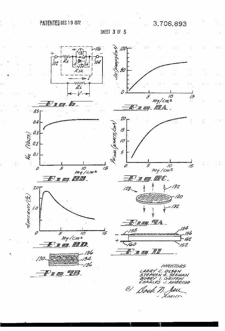
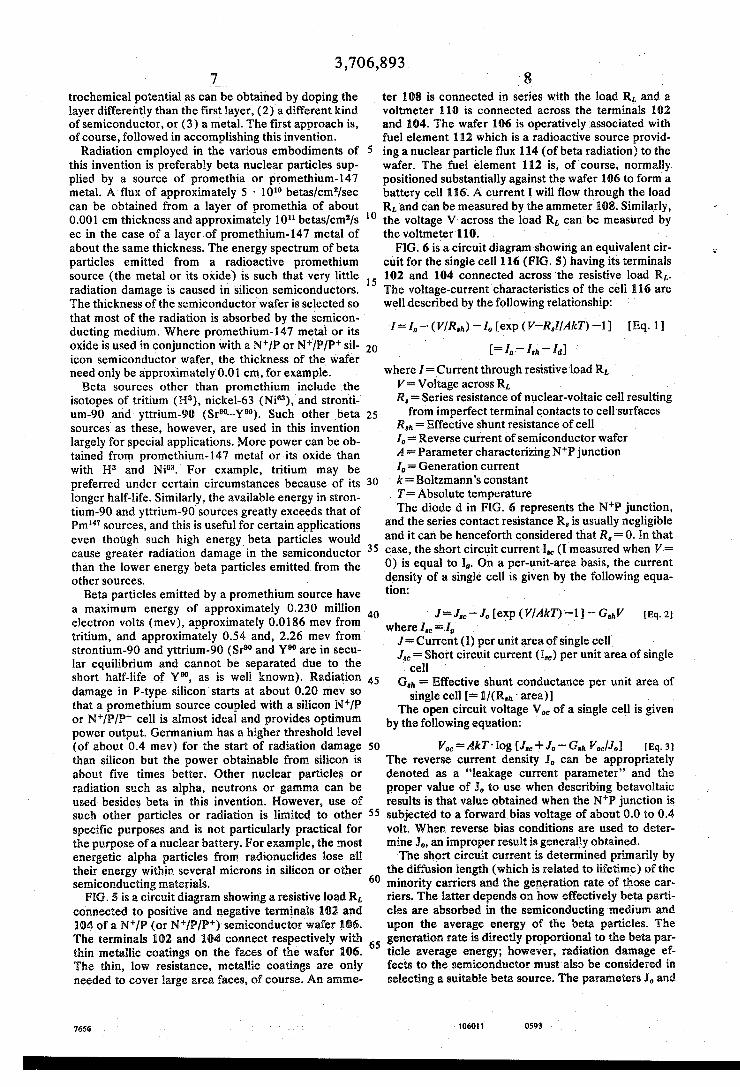
FIG. 5 is a circuit diagram showing a resistive load RL connected to positive and negative terminals 102 and 10A of a NH? (or N+/P/P+) semiconductor wafer 106. The terminals 102 and 104 connect respectively with thin metallic coatings on the faces of the wafer 106. The thin, low resistance, metallic coatings are only needed to cover large area faces, of course. An amme
7656
20
25
30
35
45
50
55
60
65
8 ter 108 is connected in series with the load RL and a voltmeter 110 is connected across the terminals 102 and 104. The wafer 106 is operatively associated with fuel element 112 which is a radioactive source provid ing a nuclear particle ?ux 114 (of beta radiation) to the wafer. The fuel element 112 is, of course, normally positioned substantially against the wafer 106 to form a battery cell 116. A current I will ?ow through the load RLland can be measured by the ammeter 108. Similarly, the voltage V across the load RL can be measured by the voltmeter 110. .
FIG. 6 is a circuit diagram showing an equivalent cir cuit for the single cell 116 (FIG. 5) having its terminals 102 and 104 connected across ‘the resistive load RL. The voltage-currentcharacteristics of the cell 116 are well described by the following relationship: '
I= I, — (V/Rm) — I, [exp (V-RJ/AkT) Q-l] [Eq. I]
‘ [= I..- 1.. - 1.1
where I =_Current through resistive load RLv V= Voltage across RL R,= Series resistance of nuclear-voltaic cell resulting from imperfect terminal contacts to'cell surfaces
R,“ = Effective shunt resistance of cell I, = Reverse current of semiconductor wafer A = Parameter characterizing N+P junction 1,7 = Generation current k = Boltzmann's constant
. T= Absolute temperature
The diode d in FIG. 6 represents the N+P junction, and the series contact resistance R, is usually negligible and it can be henceforth considered that R, = 0. In that case, the short circuit current I” (I measured when V: 0) is equal to 1,. On a per-unit-area basis, the current density of a single cell is given by the following equa tion:
J=J,,, —-J,, [exp (V/AkT) —l 1 — G,,,.V [Eq. 21 where I,c =1, _ '
J = Current (I) per unit area of single cell J,c = Short circuit current (I,,,) per unit area of single
cell G". = Effective shunt conductance per unit area of
single cell [= 1/(Rm ' area)] The open circuit voltage V0,, of a single cell is given
by the following equation:
V,Jc = AkT- log [1,, + Jo -— G," Voc/J? [Eq. 3] The reverse current density .Io can be appropriately denoted as a “leakage current parameter” and the proper value of Jo to use when describing betavoltaic results is that value obtained when the N‘“? junction is subjected to a forward bias voltage of about 0.0 to 0.4 volt. When reverse bias conditions are used to deter mine .I.,, an improper result is generally obtained. The short circuit current is determined primarily by
the diffusion length (which is related to lifetime) of the minority carriers and the generation rate of those car riers. The latter depends on how e?‘ectively beta parti cles are absorbed in the semiconducting medium and upon the average energy of the beta particles. The generation rate is directly proportional to the beta par ticle average energy; however, radiation damage ef fects to the semiconductor must also be considered in selecting a. suitable beta source. The parameters I, and
1060M 0593
3,706,893 9
A are tightly coupled, and these parameters re?ect the quality of the semiconductor element or device. In the case of an ideal silicon NP junction, .10 is about 10'11 amp/cm2 and A = 1.0. In real devices, however, defects on the surface and near the junction change these values considerably. For example, in the voltage range of interest, typical commercial silicon solar cells are characterized by values of .10 of the order of 10'6 amp/cm2 and A of approximately 2.5. The net effect of the change in. values from the ideal
case is that Vac of the device is considerably lowered, and the maximum power is also lowered. The existence of defects in the junction region causes electron-hole recombination currents —or leakage currents- that subtract from the available output current. Surface de fects also account for losses, but the junction recom bination currents are the primary reason for solar cells not behaving as ideal cells under low bias voltage con ditions. The parameter G,“ takes into account current shunting paths which are, of course, sources of loss in a betavoltaic energy converter. The paths can arise from inhomogeneities in the planar junction, or defective re gions near the edge of the device. Commercial silicon solar cells have values of G8,, of about 10'“ ohm‘1 cm'”. Thus, if the effective area of such a cell is 1 cm2, the shunt resistance, R8,, = 1/(G,,,I ' area), would be about 105 ohms. FIG. 7 is a graph illustrating the J~V and Pw-V
characteristics of a single cell constructed according to our invention. The cell had a planar junction area of 2.85 cm2 and was fueled with a promethium-147 radioisotope, by utilizing a promethia source having an area of 2.3 8 cm2 and a layer thickness of approximately 5.3 mg/crn’. Promethia activity was approximately 678 curies/gm such that a total source strength of 1288 microwatts/cm2 was available. Such cells or devices are much more suited to betavoltaic energy conversion than the solar cells mentioned above. Devices of the nature as that having the typical betavoltaic data of FIG. 7 are characterized by the following parameters: 10510‘9 amplcmz, AELS and G,,,E(0.5 ' 10"’) ohm“1 cm'”. With the promethium-147 radioisotope fuel, the energy spectrum of beta particles emitted therefrom is such that very little radiation damage occurs in silicon devices. The J-V characteristic of the single cell fueled with
promethium-147 is shown at the “beginning of life” by a full line 118 in FIG. 7, and is shown by broken lines 120, 122 and 124 after 1, 2 and 3 years, respectively. The beginning of life output power density (Pw) availa ble from a single cell (output power per unit area of its active area) is shown by a full line 126. The short cir cuit current density .1“ generally decays as does the promethium-147 radioisotope (of 2.6 years half-life). Further, the single cell open circuit voltage V0c decays as follows:
V0C = ( V,,,.),=0 — (0.0067 )At where t = Elapsed time (years) _
The net effect on the value of maximum power (Pm) is that it also decays, with a half-life of (ll/2),, 52.13 years. At the maximum power point in FIG. ‘7, efficien cy of the exemplary cell is 1.1 percent. The efficiency is based on the total amount of power available from the promethia source.
[m 41
7657
15
25
35
45
55
60
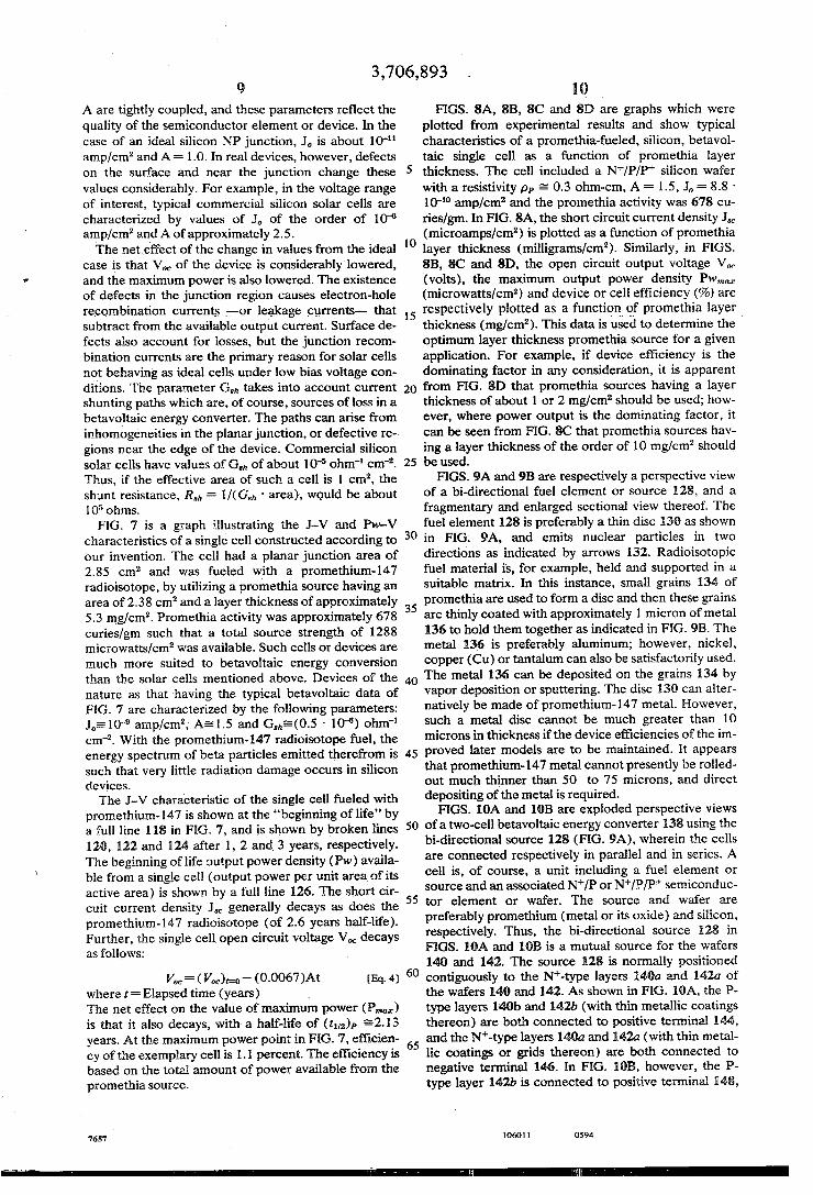
10 FIGS. 8A, 8B, 8C and 8D are graphs which were
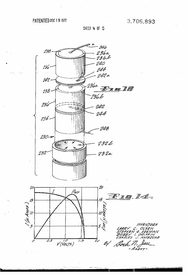
plotted from experimental results and show typical characteristics of a promethia-fueled, silicon, betavol taic single cell as a function of promethia layer thickness. The cell included a N"'/P/P+ silicon wafer with a resistivity pp 5 0.3 ohm~cm, A = 1.5, .10 = 8.8 - 10'1o amp/cm2 and the promethia activity was 678 cu ties/gm. In FIG. 8A, the short circuit current density J,c (microarnpslcmz) is plotted as a function of promethia layer thickness (milligramslcmz). Similarly, in FIGS. 8B, 8C and 8D, the open circuit output voltage Voc (volts), the maximum output power density Pwmu (microwatts/cm”) and device or cell efficiency (%) are respectively plotted as a function of promethia layer thickness (mglcmz). This data is used to determine the optimum layer thickness promethia source for a given application. For example, if device efficiency is the dominating factor in any consideration, it is apparent from FIG. 8D that promethia sources having a layer thickness of about 1 or 2 mg/cmz should be used; how ever, where power output is the dominating factor, it can be seen from FIG. 8C that promethia sources hav ing a layer thickness of the order of 10 mg/cm2 should be used.
FIGS. 9A and 9B are respectively a perspective view of a bi-directional fuel element or source 128, and a fragmentary and enlarged sectional view thereof. The fuel element 128 is preferably a thin disc 130 as shown in FIG. 9A, and emits nuclear particles in two directions as indicated by arrows 132. Radioisotopic fuel material is, for example, held and supported in a suitable matrix. In this instance, small grains 134 of promethia are used to form a disc and then these grains are thinly coated with approximately 1 micron of metal 136 to hold them together as indicated in FIG. 9B. The metal 136 is preferably aluminum; however, nickel, copper (Cu) or tantalum can also be satisfactorily used. The metal 136 can be deposited on the grains 134 by vapor deposition or sputtering. The disc 130 can alter natively be made of promethium-l47‘metal. However, such a metal disc cannot be much greater than 10 microns in thickness if the device efficiencies of the im proved later models are to be maintained. It appears that promethium-147 metal cannot presently be rolled out much thinner than 50 to 75 microns, and direct depositing of the metal is required.
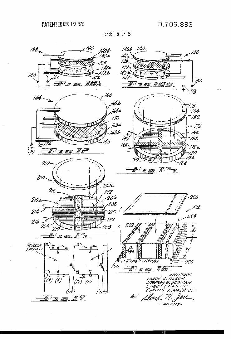
FIGS. 10A and 10B are exploded perspective views of a two-cell betavoltaic energy converter 138 using the bi-directional source 128 (FIG. 9A), wherein the cells are connected respectively in parallel and in series. A cell is, of course, a unit including a fuel element or source and an associated N+/P or N+/P/P+ semiconduc tor element or wafer. The source and wafer are preferably promethium (metal or its oxide) and silicon, respectively. Thus, the bi-directional source 128 in FIGS. 10A and 10B is a mutual source for the wafers 140 and 142. The source 128 is normally positioned contiguously to the N+-type layers 140a and 142a of the wafers 140 and 142. As shown in FIG. 10A, the P type layers 140b and 142b (with thin metallic coatings thereon) are both connected to positive terminal 144, and the N+-type layers 1470a and 142a (with thin metal lic coatings or grids thereon) are both connected to negative terminal 146. In FIG. 108, however, the P type layer 1421: is connected to positive terminal 148,
106011 0594
3,706,893 11
the N+-type layer 142a is connected to the P-type layer 1401; and the N+-type layer 1411a is connected to nega tive terminal 151).
FIG. 11 is an elevational view of an NW1’ (or N?P/P’r semiconductor wafer 152 having a coating 1543 of promethium-l47 metal or promethia deposited directly onto the N+-type layer 156 of the wafer 152. The promethium coating 154 can be deposited directly onto the surface of the N’?type layer 156 either by vapor deposition, sputtering or electroplating techniques. Negative electrode strip 158 is bonded to the N+-type layer 156 at its peripheral margin (which has a thin metallic coating thereon), and positive elec trode strip 161) is bonded to the (thinly metal coated) P-type (or P+-type) layer 162 at its peripheral margin as illustrated. The surface of the N'+-type layer 156 pro vides direct support for the promethium coating 154, and an intervening conductive metal coating or grid is not used. The advantages include greater simplicity of construction and signi?cantly increased ef?ciency.
FIG. 12 is an exploded perspective view of a two-cell betavoltaic energy converter 164 having a radioactive material coated on at least one semiconductor wafer. The converter 164 includes N+/P of an enclosing pair, (or N+/P/P+) semiconductor wafers 166 and 168. The N+-type layer 168a of the wafer 168 has a coating 170 thereon of promethium-147 metal or promethia, for ex ample, just as the wafer 152 (FIG. 11). The wafer 166 need not have a radioactive coating thereon and is nor mally positioned with its N‘r-type layer 166a contiguous to the coating 171) to take advantage of its emitted nuclear particles. Of course, the N‘L-type layer 166a can have a coating thereon similar to the coating 170. In this instance, each of such coatings can be formed with a significantly lower layer thickness. The two cells of the converter 164 are shown connected in parallel to the positive and negative terminals 172 and 174; how ever, it should be clear that the cells can be readily con nected in series to the terminals 172 and 174. Of course, the‘ faces of the P-type (or P+-type) layers 16617 and 168b have thin metallic coatings thereon, and the marginal ring areas of the N+-type layers 166a and 168a also have such coatings thereon. FIG. 13 is an exploded perspective view of a highly
compact and practical form of a nuclear battery 176. Most applications require several cells in a nuclear bat tery. The voltage requirements determine the number of cells to be connected in series, while the current requirements determine the cell areas and/or the number of cells to be connected in parallel. The ?nal design, therefore, includes one or more cells combined in a series and/or parallel network to meet required speci?cations. For example, the nuclear battery 30 em bodiment shown in FIG. 1 is a series connection of cells, and certain models (DL-lOA-2 and DL-IOOA 1) thereof meet the following speci?cations. '
Model DL-lOA-Z DL-IOOA-l
Maximum powenPn" . (microwatts) 43 2l2
Voltage at PM, (volts) 1.35 3.35 Open circuit voltage, V“
(volts) [.79 4.75 Short circuit current, 1,,
(microamps) 44.0 77.0 Length of cylindrical
envelope, L (cm) 0.57 1.22 Diameter of cylindrical
7658
25
30
45
55
60
65
12 envelope, D (cm) l.l 8 1.55
Device efficiency (%) 1.04 0.84
The planar, multiple section, cell embodiment of the nuclear battery 176 can meet the above speci?cations ' (taken on a per-cell basis) with relatively greater com pactness and, certainly, with a simpler construction than that of the battery 30. The battery 176 includes a, fuel element 178 and a multiple section N+IPIP+ semiconductor element 180. The fuel element 171%. comprises a disc 182 and a thin coating 1841 of radioac tive material thereon. The disc 182 is made‘of alu minum and the coating 184 is of promethia, for exam ple. Thesemiconductor element 180 can be made by ?rst diffusing phosphorus into the upper‘ surface active areas of a P-type silicon wafer 186 using a suitable mask (not shown) to produce a N+-type layer 188 thereon. Boron is then similarly diffused into the lower surface active areas of the wafer 186 to produce a P* type layer 190 thereon. The wafer 186 is next cut into appropriate sectors 192 which are suitably cemented back together in disc form to an electrically insulating cross 192a made of material such as ceramic. In one construction, the sectors 192 were cemented directly on the surface of a ceramic substrate plate so that the cross 192a was of air. The sectors 192 were connected in series by (three) leads 194 which connect a N+-type layer 188 of one- sector to the P+-type layer 190 of a succeedingv sector in a clockwise direction. Positive output lead 196 is connected to the P+-type layer of the first (upper left) sector, and negative output lead 198 is connected to the N+-type layer of the last (lower left) sector of the semiconductor element 180. As in the other versions of this invention, the surfaces of the N* type and P+-type layers 188 and 190 of each sector 192 have a thin metallic coating provided thereon.
FIG. 14 is a graph of the current (I) and power (Pwr) versus voltage (V) characteristics of a planar, four sec tion cell, nuclear battery embodiment similar to that shown in FIG. 13. The semiconductor element was coupled to a promethia fuel element or source wherein the fuel disc ,is coated with. promethia at a layer thickness of approximately 8 mg/crn2 and having an ac tivity of about 660 curies/gm. It can be noted that max imum power occurs at a relatively high voltage, for a single cell con?guration.
FIG. 15 is anexploded perspective view of a planar, multiple section, cell embodiment of a nuclear battery 269 which is superior from a fabrication point of view than the battery 176 of FIG. 13. The battery 201) in cludes fuel element 202 and a multiple section N’rll’lli”r semiconductor element 204;. In this con?guration, P type (silicon) wafer 206 need not be cut into sectors since P'i-type layers 208 and N+-type layer 216 are formed by deep diffusion or ion implantation (ion beam directed into material) techniques in the wafer as axial guard and isolating walls, respectively, and completely separate and isolate each cell section. The P+-type wall layers 208 are located between the planar N’f-type layers 210a and the N+-type_ wall layer 2111. The wall layer 210 can be ceramic but this would require cutting of the wafer 206. The cell sections can be connected in series by (three) leads 212, and posi tive and negative output leads 2111 and 216 are con nected to the first and last sections as illustrated. The
l060ll 0595
3,706,893 13
exposed surfaces of the guard layers 20% and of the planar layers Elba are, of course, plated with a thin metallic low resistance coating. it may be noted that a single cell including a promethia source and a silicon N"? or NVP/Pf wafer, and which utilizes only one ac tive area or section, supplies electrical power charac teristically at voltages of about 0.3 volt. Thus, multiple section cell embodiments of nuclear batteries are highly desirable to obtain much higher output voltages from a relatively compact device.
FIG. 16 is a partially fragmentary and exploded per spective view of a laminar, multiple section, cell con ?guration of a nuclear battery 218. The battery 218 in— cludes a fuel element 220 and a multiple section NVP/l’+ semiconductorelement 222. The illustrated structure is believed to be self-explanatory in view of the preceding description on multiple section cell em bodiments. The laminar, multiple section battery 218 may at ?rst sight appear to be equivalent to the planar devices of FIGS. i3 and 15. It is not, however. The nuclear particle flux 224 is parallel to the main N+P+ junctions in this embodiment. The silicon semiconduc tor element 222 preferably has, for example, a height h greater than approximately 1.00 microns and a width w of the order of 1 cm. These dimensions can be varied by using another fuel element similar to the fuel ele ment 22f) on the opposite (lower) side of the semicon ductor element 222, and also on the front and rear sides thereof. One of the advantages of this battery (218) con?guration is that very high voltage devices can be easily made by having any desired number of lateral cell sections. The lateral end surfaces have, of course, metallic coatings deposited thereon to which are soldered the positive and ‘negative electrode strips 226 and 228.
FlG. K7 is an electron energy level diagram for about two sections of the NVP/P‘l semiconductor element 222 shown in H6. 16. its operation under exposure to radiation is indicated in the diagram. It can be seen from the diagram that the main junctions are those between the N+-type and P+-type layers. Current flows from the electrode strip 226 (FIG. 16) attached to the coated left end W-type layer and to the electrode strip 228 attached to the coated right end N+-type layer when a load is connected between the electrode strips.
P16. 118 is an exploded and partly fragmentary per spective view of a “needle-like” or elongated cylindri cal, multiple section, cell embodiment of a nuclear bat tery 236. The battery 230 is fabricated in a manner generally similar to that of the planar battery 176 of H6. 13. The battery 23% includes a fuel element 232 and a multiple section N+IP (or NVP/P") semiconduc tor element 234. in this instance, however, the fuel ele ment 232 comprises a thin cylindrical shell 232a of, for example, aluminum foil having a promethia layer 23% deposited on its inner surface. The semiconductor ele ment 23d is fabricated by di?using phosphorus circum ferentially into a P-type cylinder of semiconductor material. The cylinder is then cut into uniform sections 236 having a P-type core 236a and a surrounding N* type outer layer 23617. The normally upper surface of the P-type core 236a is covered with a metallic coating or sheet 238 which can be aluminum, and the circum ferential surface of the N+-type layer 236i: is covered
‘ with a metallic grid or thin metallic coating 2% which
7659
20
25
30
35
40
45
50
55
60
M can also be of aluminum. The periphery of the coating or sheet 23% covering the normally upper surface of the P-type core 236a is, of course, spaced from the N“? junction so that there is no interaction therewith. For a N+/P/P+ semiconductor, the coating 238 would be deposited on top of a central P+-type cylinder formed axially in the P-type core 236a. The sections 236 are separated by insulator discs 242
which are preferably made of ceramic. Each disc 242 has a hole 242a through which passes a lead 244 con necting a P-type core 236a of one section 236 to the N+-type layer 236b of an adjacent upper section. The sections 236 are thus connected in series with a positive output lead 246 and a negative output lead 248. The in sulator discs 242 can be cemented or suitably secured to adjacent sections 236, and then inserted and posi tioned in the cylindrical fuel element 232 shell. While a cylindrical junction surface is utilized in obtaining the elongated cylindrical battery 230, it is apparent that other con?gurations of nuclear batteries can be ob tained so'long as a suitable junction'can be formed therein.
It is to be understood that the exemplary embodi ments of this invention are merely illustrative of, and not restrictive on, our broad invention and that various changes in design, structure and arrangement may be made therein without departing from the true spirit and scope of the invention. We claim: 1. In a nuclear battery, a cell comprising: a fuel element including a radioactive source of
nuclear particles having a known maximum ener gy, said radioactive source comprising a source of beta particles; and
a semiconductor element positioned in at least close proximity to said fuel element and irradiated by the same, said semiconductor element including a semiconductor wafer and relatively thin, electri cally conductive, distributed ohmic contact mem bers provided on respective faces of said wafer, and said wafer comprising a system of at least a high carrier concentration ?rst-type layer and a lower carrier concentration second-type layer of semiconductor material having respectively dif ferent electrochemical potentials and having an energy threshold level of radiation damage com patible with, and at least of the same order as, the maximum energy of said nuclear particles, said layers having a junction therebetween and said fuel element being positioned operatively close to said junction adjacent to said high carrier concen tration ?rst-type layer, at least said ohmic contact member adjacent to said fuel element providing a relatively large fractional open area for passage therethrough of said nuclear particles whereby a long life cell of maximum output voltage and high power output is obtained.
2. The invention as defined in claim 1 wherein said fuel element includes a unitary radioactive source member, and said wafer system further comprises a high carrier concentration layer of said second-type electrochemical potential material, said latter layer serving primarily ‘as a re?ector barrier whereby a long life cell of maximum output voltage and high power output is obtained.
1060\1 0596
t5 , 3. The invention as de?ned in claim 2 wherein said
source member includes a backing disc having a layer of radioactive material provided on a surface thereof and which is a promethium source of beta particles, and said system includes a silicon system of N’i-type, P- . type and P+-type layers of different electrochemical potential material and having carrier concentrations of the order of approximately 10'”, 1016 and 1019 atoms/cm“, respectively, said N+-type and P-type layers having said junction therebetween, said P+-type layer serving primarily as said re?ector barrier and said, fuel element being positioned operatively close to said junc tion adjacent to said N*-type layer. ‘ - '
4. The invention as de?ned in claim ll wherein said fuel element includes a bi-directional source which is a unitary radioactive disc member comprising promethia and a matrix to hold and support said promethia, and said semiconductor element is positioned in at least close proximity to one side of said» bi-directional source, and further comprising another similar semiconductor element positioned symmetrically to the other side of said bi-directional source. >
5. The invention as de?ned in claim 2 wherein said fuel element is of a planar form, and said semiconduc torelement is of a correspondingly similar planar form and having multiple sections which are insulated from each other and operatively connected in at least a par tially series arrangement to provide an output voltage higher than that available from a commensurate cell having a unitary semiconductor element.
.6. The invention as de?ned in claim 2 wherein said fuel element is of a planar form, and said semiconduc tor element is of a laminar form having laterally disposed multiple sections with planes oriented perpen dicularly to the plane of said fuel element, said sections being operatively coupled in series to provide an output voltage higher than that available from a commensu rate cell having a unitary semiconductor element.
7. The invention as de?ned in claim 1 wherein said fuel element is of an elongated and hollow cylindrical ‘form, and said semiconductor element is of a cor respondingly elongated and solid cylindrical form posi tioned concentrically within said fuel element and hav ing axially disposed multiple sections which are insu lated from each other and operatively connected in at least a partially series arrangement to provide an out put voltage higher than that available from a commen surate cell having a unitary semiconductor element.
8. The invention as de?ned in claim ll wherein said fuel element includes a unitary radioactive source member comprising a backing disc having a layer of radio-active material provided on a surface thereof and which is a promethium source of beta particles, and said system includes a silicon system of N’rétype and P type layers of different electrochemical potential material and having carrier concentrations of the order of approximately 1019 and 1016 atoms/cm“, respective- . ly, said N+-type and P-type layers having said junction therebetween and said fuel element being positioned operatively close to said junction adjacent to said N" type layer.
9. A nuclear battery comprising: a plurality of cells arranged in a series stack, each of
said cells including
7660
3,706,893
20
25
30
35
45
50
55
60
65
16 a fuel element comprising a radioactive source of
nuclear particles having a known maximum energy, said fuel element including a unitary radioactive source member, and - '
a semiconductor element positioned in at least close proximity to said fuel element and, ir radiated by the' same, said semiconductorele ment comprising a semiconductor wafer and relatively thin, I electrically conductive, dis
I tributed ohmic contact members provided on respective faces of said wafer, and said wafer in— cluding a system of atleast a high carrier con centration ?rst-type layer and a lower carrier concentration second-type layer'of semiconduc tor material having respectively different elec trochemical ‘potentials and having an energy threshold level of 'radiation’damage compatible with, and'at least of the same order as, the max imum 'energy of said nuclear particles, said layers having a junction therebetween and said fuel element being positioned operatively close to said junction adjacent to said high carrier concentration ?rst-type layer; '
a'plurality of electrically conductive ring members corresponding in number to said cells and posi tioned concentrically about said fuel elements, respectively;
electrically conductive end members sandwiching said cells of said stack, said ring members axially contacting said end members and said ohmic contact members of said wafers and providing a series connection from one of said end members through said semiconductor elements of said cells to the other of said end members;
spring means for biasing and maintaining said end members and cells of said stack in effective se ries contact throughout the same; and
a pair of electrode terminals adapted to be con nected respectively to said end members, whereby a long life battery of maximum output voltage and high power output is obtained.
10. A nuclear battery comprising: a fuel element including a radioactive source of
nuclear particles having a known maximum ener gy, said fuel element being of a planar form; and
a semiconductor element positioned in at least close proximity to said fuel element and irradiated by the same, said semiconductor element being of a correspondingly similar planar form to said fuel element and including multiple sections which are insulated from each other and electrical leads operatively connecting said sections in at least a partially series arrangement to-provide a higher output voltage therefrom, each of said sections comprising a semiconductor wafer and relatively thin, electrically conductive, distributed ohmic contact members provided on respective faces of said wafer and connecting with said leads, and said wafer including a system of at least a high carrier concentration ?rst-type layer and a lower carrier concentration second-type layer of semiconductor material having respectively different elec trochemical potentials and having an energy threshold level of radiation damage compatible with, and at least of the same order as, the max
l060ll 0597
3,706,893 17
imum energy of said nuclear particles, said layers having a junction therebetween and said fuel ele ment being positioned operatively close to said junction adjacent to said high carrier concentra tion ?rst-type layer whereby a long life battery of maximum output voltage and high power output is obtained.
11. The invention as de?ned in claim 9 wherein said source member includes a backing disc having a layer of radioactive material provided on a surface thereof and which is a promethium source of beta particles, at least said ohmic contact member adjacent to said fuel element provides a relatively large fractional open area for free passage therethrough of said nuclear particles, said system includes a silicon system of at least Nf-type and P-type layers of different electrochemical potential material and having carrier concentrations of the order of approximately 1019 and 10‘6 atoms/cm‘, respective ly, said N+-type and P-type layers having said junction therebetween and said fuel element being positioned operatively close to said junction adjacent to said N* type layer, and said spring means includes an electri cally conductive spring ring . for axially biasing uniformly over a wide base against one of said end members of said stack, and further comprising a shield
7661
30
35
40
45
50
55
60
65
18 ing container for containing and primarily providing radiation protection containment of said stack, and a fire container for containing said shielding container and primarily providing high temperature protection containment of said stack, one of said electrode ter minals being mounted on and insulated from said fire container and said spring ring electrically connecting the one of said end members to said shielding container which is in electrical contact with said ?re container sewing as the other of said electrode terminals.
12. The invention as defined in claim 10 wherein said fuel element includes a unitary radioactive source member which is a promethium source of beta parti cles, at least said ohmic contact member adjacent to said fuel element provides a relatively large fractional open area for free passage therethrough of said nuclear particles, and said system includes a silicon system of at least N+-type and P-type layers of different elec trochemical potential material and having carrier con centrations of the order of approximately 1019 and 1016 atoms/cm“, respectively, said N+-type and P-type layers having said junction therebetween and said fuel ele ment being positioned operatively close to said junc tion adjacent to said N+-type layer.
0598