numerical methods for shape optimization of …
TRANSCRIPT

NUMERICAL METHODS FOR SHAPE OPTIMIZATION OFPHOTONIC NANOSTRUCTURES
Zur Erlangung des akademischen Grades einesDOKTORS DER NATURWISSENSCHAFTEN (Dr. rer. nat.)
von der KIT-Fakultät für Physikdes Karlsruher Instituts für Technologie (KIT)
angenommeneDISSERTATION
vonM. Sc. Xavier García Santiago
am Institut für Theoretische Festkörperphysik
Tag der mündlichen Prüfung: 27. November 2020Referent: Prof. Dr. Carsten RockstuhlKorreferent: Prof. Dr. Thomas Pertsch

This document (with the exception of reprinted figures for which the copyright is held bythe respective journal) is licensed under theCreative CommonsAttributionShareAlike 4.0International License. To viewa copy of this license, visit https://creativecommons.org/licenses/by-sa/4.0/.

Abstract
Inverse design is an important discipline in any field of engineering and science. Op-tics and photonics is not an exception. Together with improved fabrication technologies,design optimization is one of the main drivers of the tremendous advances in photonictechnologies. The appearance of modern computers and software, able to solve electro-magnetic field propagation problems, semi-automatized the tasks of design optimiza-tion. The final goal of this field would be to achieve full automation. That means, a de-sign process completely computer-driven, able to find optimal designs, compatible withavailable fabrication processes, and without involving in the process the intuition andknowledge of the researcher or designer.
The optimizationmethods that get close to this idea are freeform shape optimization andtopology optimization. The efficiency of both methods strongly relies on another com-putational ability related to solving electromagnetic field propagation: the computationof shape and material derivatives. Developments to achieve this ability are a fundamen-tal building block of this thesis and they appear, in one way or another, throughout allchapters.
In this thesis, we study different numerical tools for computational inverse design ofphotonic structures. We focus on global optimization, as opposed to local optimizationmethods, and we investigate the use of a technique borrowed from the field of machinelearning, Gaussian processes, to do global optimization using, at the same time, shapeandmaterial derivatives. We contribute to this field proposing two numerical techniquesto improve the performance of Gaussian processes in the optimization of photonic struc-tures.
Furthermore, we design and study the performance of two photonic structures that areinteresting from theoretical and technological aspects: maximally electromagnetic chiralscatterers and waveguide edge couplers. Maximally electromagnetic chiral scatterers areobjects that show an extraordinary difference in their interaction with fields of differenthelicity. Finding objects with such characteristics at optical and near infrared frequen-cies would enable a series of interesting applications. We obtain optimal designs of chiralscatterers at a wide range of illumination frequencies and highlight their extreme proper-ties when they interact with light. The other structure studied, waveguide edge couplers,is a fundamental component to improve the power efficiency of integrated photonic cir-cuits, therefore, a key component for the further development of the global optical com-munication network. We optimized and studied two types of edge couplers, includingfreeform shape designs, whose optimization lead to compact and energy efficient struc-tures. For the optimization of both photonic structures, we combined the use of Bayesianoptimization with Gaussian processes and the calculation of shape derivatives. Further-more, the design of these structures required the development of additional numericaltools, e.g., methods for the analyses of isolated scatterers, that became an important partof this thesis by themselves.


Contents
List of publications 1
1 Introduction 5
2 Theoretical background 112.1 Introduction . . . . . . . . . . . . . . . . . . . . . . . . . . . . . . . . . . . 112.2 Electromagnetic field theory . . . . . . . . . . . . . . . . . . . . . . . . . . 11
Maxwell’s equations . . . . . . . . . . . . . . . . . . . . . . . . . . . . . . . 11The wave equation . . . . . . . . . . . . . . . . . . . . . . . . . . . . . . . . 14Scattering by isolated objects . . . . . . . . . . . . . . . . . . . . . . . . . . 18The helicity operator . . . . . . . . . . . . . . . . . . . . . . . . . . . . . . . 19Waveguide theory . . . . . . . . . . . . . . . . . . . . . . . . . . . . . . . . 20
2.3 The finite element method . . . . . . . . . . . . . . . . . . . . . . . . . . . 23Description of the method . . . . . . . . . . . . . . . . . . . . . . . . . . . . 24Shape and material derivatives . . . . . . . . . . . . . . . . . . . . . . . . . 29The direct and the adjoint methods . . . . . . . . . . . . . . . . . . . . . . . 32
3 Bayesian optimization 353.1 Introduction . . . . . . . . . . . . . . . . . . . . . . . . . . . . . . . . . . . 353.2 Gaussian Processes . . . . . . . . . . . . . . . . . . . . . . . . . . . . . . . . 38
Definition . . . . . . . . . . . . . . . . . . . . . . . . . . . . . . . . . . . . . 38Gaussian process regression . . . . . . . . . . . . . . . . . . . . . . . . . . . 40Gaussian process regression with derivative information . . . . . . . . . . . 42Model selection . . . . . . . . . . . . . . . . . . . . . . . . . . . . . . . . . . 43
3.3 Bayesian Optimization Using Gaussian Processes . . . . . . . . . . . . . . . 45General description . . . . . . . . . . . . . . . . . . . . . . . . . . . . . . . 45Bayesian Optimization using derivative information . . . . . . . . . . . . . 47
3.4 Scalable Bayesian Optimization . . . . . . . . . . . . . . . . . . . . . . . . . 49The scalability problem . . . . . . . . . . . . . . . . . . . . . . . . . . . . . 49Matrix update of the Cholesky decomposition . . . . . . . . . . . . . . . . . 51Bayesian optimization with a local Gaussian process model . . . . . . . . . 54
3.5 Conclusions . . . . . . . . . . . . . . . . . . . . . . . . . . . . . . . . . . . . 57
4 Design of isolated scatterers 594.1 Introduction . . . . . . . . . . . . . . . . . . . . . . . . . . . . . . . . . . . 594.2 Decomposition of scattered fields into VSWFs using surfaces with general
shapes . . . . . . . . . . . . . . . . . . . . . . . . . . . . . . . . . . . . . . . 61Mathematical derivation . . . . . . . . . . . . . . . . . . . . . . . . . . . . . 61FEM implementation of the decomposition . . . . . . . . . . . . . . . . . . 66Decomposition of fields scattered from cylindrically symmetric objects . . 71
4.3 Calculation of the T-matrix . . . . . . . . . . . . . . . . . . . . . . . . . . . 73
iii

Contents
Description . . . . . . . . . . . . . . . . . . . . . . . . . . . . . . . . . . . . 73Example: Design of dual cylinders . . . . . . . . . . . . . . . . . . . . . . . 75
4.4 Calculation of shape and material derivatives for T-matrices . . . . . . . . 774.5 The adjoint method for multi-scattering problems . . . . . . . . . . . . . . 78
Description . . . . . . . . . . . . . . . . . . . . . . . . . . . . . . . . . . . . 78Example: metasurface hologram . . . . . . . . . . . . . . . . . . . . . . . . 81
4.6 Conclusions . . . . . . . . . . . . . . . . . . . . . . . . . . . . . . . . . . . . 83
5 Application examples 855.1 Maximal electromagnetic chiral helices . . . . . . . . . . . . . . . . . . . . 85
Introduction . . . . . . . . . . . . . . . . . . . . . . . . . . . . . . . . . . . 85Electromagnetic chirality . . . . . . . . . . . . . . . . . . . . . . . . . . . . 87Simulation setup . . . . . . . . . . . . . . . . . . . . . . . . . . . . . . . . . 88Results of the optimization . . . . . . . . . . . . . . . . . . . . . . . . . . . 91Conclusions . . . . . . . . . . . . . . . . . . . . . . . . . . . . . . . . . . . . 97
5.2 Waveguide coupler for photonic inter-chip communication . . . . . . . . . 99Introduction . . . . . . . . . . . . . . . . . . . . . . . . . . . . . . . . . . . 99Parametric waveguide coupler . . . . . . . . . . . . . . . . . . . . . . . . . 102Freeform waveguide coupler . . . . . . . . . . . . . . . . . . . . . . . . . . . 106Conclusions . . . . . . . . . . . . . . . . . . . . . . . . . . . . . . . . . . . . 111
6 Conclusions 113
Bibliography 117
Appendices 139A Definition of the vector spherical wave functions . . . . . . . . . . . . . . . 141B Multipole decomposition of a plane wave . . . . . . . . . . . . . . . . . . . 143
Acknowledgements 145
Selbstständigkeitserklärung 147
iv

List of publications
Published peer-review scientific publications
1. X. Garcia-Santiago, S. Burger, C. Rockstuhl, and P.-I. Schneider, "Bayesian optimiza-tionwith improved scalability and derivative information for efficient design of nanopho-tonic structures", Accepted for publication in Journal of Lightwave Technology (2020)
2. D. Werdehausen, X. Garcia-Santiago, S. Burger, I. Staude, T. Pertsch, C. Rockstuhl,M. Decker, "Modelling Optical Materials at the Single Scatterer Level - The Transitionfrom Homogeneous to Heterogeneous Materials", Accepted for publication in AdvanceTheory and Simulations (2020)
3. J. Feis, D. Beutel, J. Köpfler, X. Garcia-Santiago, C. Rockstuhl,M.Wegener, and I. Fernandez-Corbaton, "Helicity-preserving optical cavitymodes for enhanced sensing of chiralmolecules",Physical Review Letters, 124 (3), 033201 (2020)
4. P. Gutsche, X. Garcia-Santiago, P.-I. Schneider, K. M. McPeak, M. Nieto-Vesperinas,and S. Burger,"Role ofGeometric Shape inChiralOptics", Symmetry, 12 (1), 158 (2020)
5. A. Rahimzadegan, D.Arslan, D.Dams, A.Groner, X. Garcia-Santiago, R.Alaee, I. Fernandez-Corbaton, T. Pertsch, I. Staude, and C. Rockstuhl, "Beyond dipolar Huygens’metasurfacesfor full-phase coverage andunity transmittance",Nanophotonics, 9 (1), 75-82 (2020)
6. P.-I. Schneider, X. Garcia-Santiago, V. Soltwisch,M.Hammerschmidt, S. Burger, C. Rock-stuhl, "Benchmarking five global optimization approaches for nano-optical shape opti-mization and parameter reconstruction", ACS Photonics, 6 (11), 2726-2733 (2019)
7. F. Graf, J. Feis, X. Garcia-Santiago,M.Wegener, C. Rockstuhl, and I. Fernandez-Corbaton,"Achiral, helicity preserving, and resonant structures for enhanced sensing of chiralmolecules",ACS Photonics, 6 (2), 482–491 (2019)
8. X. Garcia-Santiago,M.Hammerschmidt , S. Burger , C. Rockstuhl , I. Fernandez-Corbaton,and L. Zschiedrich, "Decomposition of scattered electromagnetic fields into vector spher-ical wave functions on surfaces with general shapes", Physical Review B, 99 (4), 045406(2019)
9. X. Garcia-Santiago, S. Burger, C. Rockstuhl, and I. Fernandez-Corbaton, "Measuringthe electromagnetic chirality of 2D arrays under normal illumination", Optics Letters, 45(20), 4075-4078 (2017)
Submitted peer-review scientific publications
1. P. Scott, X. Garcia-Santiago, D. Beutel, C. Rockstuhl, M. Wegener, and I. Fernandez-Corbaton,"On enhanced sensing of chiral molecules in optical cavities", Submitted to Ap-plied Physics Reviews
1

List of publications
Scientific publications in preparation
1. X. Garcia-Santiago, M. Hammerschmidt, S. Burger, J. Sachs, P. Fisher, M. Knöller,T. Arens, F. Hettlich, R. Griesmaier, I. Fernandez-Corbaton, and C. Rockstuhl, "Towardsmaximal electromagnetically chiral scatterers at optical frequencies"
Conference contributions
1. X. Garcia-Santiago, P.-I. Schneider, S. Burger, and C. Rockstuhl, "Global optimiza-tion of a free-form waveguide coupler",Workshop on Theoretical and Numerical Tools forNanophotonics (TNTN2020), (Berlin, 02-2020)
2. X. Garcia-Santiago, P.-I. Schneider, S. Burger, and C. Rockstuhl, "Towards ScalableBayesian Optimization", 12th Annual Meeting Photonic Devices, (Berlin, 02-2019)
3. P.-I. Schneider, X. Garcia-Santiago, L. Zschiedrich, C. Rockstuhl, and S. Burger, "Opti-mization of quantumoptical deviceswithmachine learning approaches",WorkshopQuan-tum Optics and Secure Optical Transmission, (Berlin, 18-10-2018)
4. X. Garcia-Santiago, P.-I. Schneider, S. Burger, and C. Rockstuhl, "Shape optimizationof nanostructures with Bayesian optimization and derivative information", European Op-tical Society Biennial Meeting, (Delft 8-10-2018)
5. P.-I. Schneider, X. Garcia-Santiago, F. Binkowski ,P. Gutsche, T. Hoehne, M. Hammer-schmidt, L. Zschiedrich, and S. Burger, "Engineering electromagnetic fields in nanoscaleenvironments by numerical optimization",Workshop: Modeling, analysis, and approxima-tion theory toward applications in tomography and inverse problems, (Berlin, 08-2018)
6. P.-I. Schneider, X. Garcia-Santiago, F. Binkowski, P. Gutsche, T. Hoehne, M. Hammer-schmidt, L. Zschiedrich, and S. Burger, "Light Management for Engineering Lumines-cence in Nanoscale Environments by Numerical Optimization", 233rd ECS Meeting, (Sea-tle, 16-05-2018)
7. P.-I. Schneider, L. Zschiedrich, X. Garcia-Santiago, and S. Burger, "Optimization ofquantum optical devices with machine learning", OWTNM 2018 (Bad Sassendorf, 13-04-2018)
8. M. Hammerschmidt, P.-I. Schneider, X. Garcia-Santiago, L. Zschiedrich, and S. Burger,"Quantifying uncertainties of reconstructed parameters in optical scatterometry of nanos-tructured surfaces", 10th Workshop Ellipsometry (WSE 10), (Chemnitz, 19-03-2018)
9. P.-I. Schneider, X. Garcia-Santiago, and S. Burger, "Comparison of different optimiza-tion algorithms for improving a single-photon source", 11th Annual Meeting Photonic De-vices, (Berlin, 10-02-2018)
10. X. Garcia-Santiago, P.-I. Schneider, C. Rockstuhl, and S. Burger, "Optimization ofdiffractive optical elements usingmachine-learning approaches", SPIE PW 18, (San Fran-cisco, 30-01-2018)
11. X. Garcia-Santiago, P.-I. Schneider, C. Rockstuhl, and S. Burger, "Shape design ofa reflecting surface using Bayesian Optimization", Journal of Physics: Conference Series,963, 012003 (2018)
12. X. Garcia-Santiago “Global optimization of complex optical structures using Baye-sian optimization based on Gaussian processes", Karlsruhe Days of Optics and Photonics,(Karlsruhe, 11-2017)
13. M. Hammerschmidt, M. Weiser, X. Garcia-Santiago, L. Zschiedrich, B. Bodermann,
2

and S. Burger, "Quantifying parameter uncertainties in optical scatterometry using Baye-sian inversion", Proceedings of SPIE, 10330, 1033004 (06-2017)
14. P.-I. Schneider, X. Garcia Santiago, C. Rockstuhl, and S. Burger, "Global optimizationof complex optical structures using Bayesian optimization based on Gaussian processes",Proceedings of SPIE, 10335, 141-149 (06-2017)
15. X. Garcia-Santiago, S. Burger, C. Rockstuhl, and I. Fernandez-Corbaton, " Electro-magnetic chirality of 2D arrays under normal illumination", 10th AnnualMeeting PhotonicDevices, (Berlin, 10-02-2017)
3

List of publications
4

1 | Introduction
Optics and nanophotonics technologies provide crucial technological components to oursociety. The chips that build our computers, mobile phones, data centers and supercom-puters aremade thanks to lithographic processes [1–4]. The large internet global networkis implemented on optical fibers [5, 6], complex multi-lens systems allow the implemen-tation of compact high resolution cellphone cameras, and solar energy is a strategicaltechnology for the decarbonization of energy production [7, 8], just to name a few.
Despite the incredible advances we have witnessed in the last decades, there is a continu-ous need of improving optical technologies. The increasing demand of data rates, mainlydriven by the appearance of data centers, requires faster andmore energy efficient opticalnetworks [9, 10]. Improvements in the efficiency and costs of solar cells [11–15] are alsoof huge importance for the health of the planet and the possibility to fabricate smallerelectrical transistors enables more powerful and energy efficient computer chips. Fur-thermore, new technologies yet to reach a mature status, e.g., quantum computers [16–20], promises another revolution that could drastically shape our society as we under-stand it nowadays.
The main aspects behind the improvements in photonic technologies are better fab-rication techniques, but also the incorporation of new physical concepts and the im-provement in the designs. Decades ago, the design of the different components of aphotonic device was based on the knowledge and intuition of the researchers and devel-opers. Nowadays, this knowledge continues to play an important role. However, with theemergence of modern computers and computer programs able to solve electromagneticfield propagation problems in an affordable amount of time, the process of designing thecomponents of a photonic device has become more and more computer-driven.
Computational inverse design for photonic devices has evolved considerably along thelast three decades. The holy grail of this task is to obtain designs for photonic devices thatshow extremely good performances, that are as simple to fabricate as possible, and thatare obtained without the intervention of any person during the design process. However,quite frequently the main characteristics of the final designs obtained for the photonicstructures are fixed by the designer at the early stages of the design process. In theseinstances, the designer proposes a geometrical model in which some of their character-istics are described by a few non-fixed parameters. Then, a computer program tries tofind the optimal values for these parameters based on a function that measures the per-formance of the structure, called the objective function, obtained from electromagneticsimulations of the structure.
The two principle techniques that try to reduce the influence of human interventionin the design process are freeform shape optimization [21, 22] and topology optimiza-tion [23–26]. In freeform shape optimization, the shape of the structure is very often de-scribed using a series of b-spline curves or surfaces. The shape of the photonic structure
5

Chapter 1. Introduction
is then controlled by the weights and control points of the b-splines. In topology opti-mization, the photonic structure is discretized in, usually, thousands of different smallpixels whose material properties are to be set during the optimization process. The mainidea behind both approaches is to restrict as less as possible the geometry of the photoniccomponent aimed to be designed, and to let the optimization algorithm to identify themost optimal design in this non-restricted design space. In this sense, topology opti-mization is an even more flexible method than freeform shape optimization.
The performance of both optimization techniques is closely linked to the development ofnumerical methods that solve Maxwell’s equations and that also return the derivativesof the solution with respect to the design variables. The techniques used to compute thederivatives, the forward and the adjoint method, provide this extra derivative informa-tion adding a small computational overhead to the calculation of Maxwell’s equations.Even though both the forward and the adjoint method have been used for more thanfifteen years, a few issues remain yet to be solved, especially in the case of calculatingshape derivatives. The main issue is that shape derivatives are not easy to implement forcomplicated structures, which are the result of applying multiple geometrical operationsin a computer aided design software. The integration of shape derivatives within CADsoftware in a fully automated manner is a rather complicated task. Another issue is thatmost of the commercial software packages available for solving Maxwell’s equations donot integrate the feature of providing the shape or material derivatives for all the offeredpost-processing quantities derived from the solution of Maxwell’s equations. This aspectalso limits the applicability of the methods.
However, the main problem that limits the applicability of both the freeform shape opti-mization and topology optimization methods is the difficulty to incorporate fabricationconstraints within the optimization process. Although thesemethods can lead to designswith remarkable performances, in most of the cases these designs are also extremely dif-ficult to implement with the available fabrication techniques. Effort is being put into thisproblem and some methods to obtain more robust designs have been proposed [27–31].However, it is still not possible, in general, to efficiently integrate into the optimizationprocess all the constraints emerging from the technological limits of the fabrication tech-niques. This is one of the reasons why even if nowadays both freeform optimization andtopology optimization can be considered standard methods within the field of photonicdesign, many photonic structures are still designed using other approaches, such as theuse of conventional parametric models.
A second limitation of any inverse design process, no matter which parametrization isused, has to do with the capacity of a computer to find the most optimal design withina given design space. In multimodal optimization problems, where the objective func-tion has multiple local minima, the time needed to explore the entire design space growsexponentially with respect to the number of dimensions of the design space. Once as-sumed that this exploration is not possible to be done, the use of optimization algorithmsaims to find a design as good as possible constrained to the amount of time availablefor this required task. The optimization algorithm is an important aspect of the designprocess. There is a wide range of optimization algorithms available and one needs tochoose among them depending on the characteristics of the problem to optimize. Drivenby the advances and the research effort that has been put in the field of machine learn-ing, different machine learning techniques have been borrowed to solve photonic inversedesign problems [32]. The goal of both fields is similar, machine learning aims to learnthe response of a system of many input variables using the least number of observationdata points. Inverse design aims to obtain the input point with the highest value of theobjective function using the least number of observation data points. Among the differ-
6

ent techniques borrowed from the field of machine learning, different works proposesthe use of convolutional neural networks [33–38] to perform inverse design of photonicstructures. However, as this technique usually requires large amounts of data, it is lim-ited to problems where one can generate large sets of observation data points. Therefore,the technique is limited to problems where it is possible to obtain fast solutions of theelectromagnetic field. Another optimization method that uses techniques of machinelearning, and that we investigate in this work, is Bayesian optimization with Gaussianprocesses. Bayesian optimization does a fully statistical treatment of the objective func-tion to obtain optimal values with the least number of observations. Moreover, Gaussianprocesses can incorporate derivative information fully analytically, allowing to exploitthe use of shape derivatives. The main drawback that limits the applicability of Gaus-sian processes is their bad scaling with respect to the number of observation data points,whichmakes the optimization to become slower and slower with each observation added.Therefore, its use is usually suggested only for the optimization of computationally ex-pensive problems. In this thesis we discus this topic of the scaling and propose differ-ent methods to reduce the scalability issues of Gaussian processes in Bayesian optimiza-tion.
Regarding this thesis, the initial goal of this PhD project was to design different opti-cal nanostructures in which we were interested from both theoretical and practical per-spectives. The project started with a few clear ideas, we had available a tool to simulateelectromagnetic field propagation in nanostructures that also provides shape derivativesand we wanted to see how we could use it to design the different photonic structureswe were interested in. As inevitably in any research project, along this process differ-ent problems and questions with regards to the optimization process started to appear,e.g., the calculation of shape derivatives in complicated geometries, the lack of sometools that we needed for the design of isolated scatterers, questions about how to takethe most out of the information provided by the shape derivatives, the scalability prob-lem of Gaussian processes, etc. This thesis became a result of this process to solve theproblems and to answer the questions that arose during the process of optimization ofthe different photonic structures. It tries tomake amodest contribution to the enormousfield of research of photonic inverse design. Along the thesis, we contribute to differenttopics of relevance for the design of photonic structures: optimization algorithms, nu-merical methods to solve or to measure relevant quantities of electromagnetic fields, orthe calculation of shape derivatives for complicated geometries.
Still, even if the development of all these tools became an important part of the work, theinitial goal of the project was not forgotten during this process. We have applied all thismethods to design different photonic structures. Emphasis was put into the design ofoptimal electromagnetic chiral scatterers and the design of compact and energy efficientfreeform waveguide edge couplers. Both of them are discussed in this document.
The optimization of chiral helices is a relevant topic from a theoretical point of view. Itis interesting to know how feasible it is to obtain, at optical and mid-infrared frequen-cies, scatterers with the extraordinary properties that maximal electromagnetically chi-ral objects present. Once available, of course, they would also unlock interesting appli-cations. On the other side, edge couplers are components of crucial importance for thedevelopment of photonic integrated circuits as they can connect different components ofphotonic chips. Photonic integrated circuits have numerous applications, but one of spe-cial relevance for our near future is their use in communication optical networks. There,photonic integrated circuits are a key element for achieving reductions in energy con-sumption and increments in data rates. In this context, the design of more efficient andmore compact edge couplers is a task of great interest from a general perspective.
7

Chapter 1. Introduction
Structure of the thesis
The thesis is structured into six chapters. After this introductory chapter, a theoreticalbackground chapter is presented. This second chapter is divided into twomain parts. Thefirst part introduces the basic electromagnetic theory that is needed along the thesis. Itstarts from Maxwell’s equations and describes some of its most fundamental solutions:the plane waves and the vector spherical wave functions. After that, it continues with theintroduction of the scattering problem, the helicity operator and its link to circularly po-larized waves, and the basics of waveguide theory. The second part of the second chapteris devoted to the introduction of the finite elementmethod. It will be themain techniqueto solve Maxwell’s equations in this thesis. This part starts with the description of themain properties of the finite element method. After the working principles of the finiteelementmethod are presented, the chapter continues with the description of the calcula-tion of the shape and material derivatives. Finally, the chapter ends with the descriptionof the twomain different techniques used to calculate the shape derivatives for a numberof different design variables: the forward and the adjoint method. As we will see, thecalculation of the shape derivatives is a tool of special relevance in this thesis, and all theother chapters to come are linked, in one way or another, to this important tool for thefield of inverse photonic design.
The third chapter is about the use of Bayesian optimization with Gaussian processes todesign photonic structures. It starts with a description of Gaussian processes and Gaus-sian process regression. One section of the chapter is devoted to the description of theincorporation of derivative information into the Gaussian process model. After that, thechapter continueswith the description of Bayesian optimization, particularly, it describeshow Gaussian processes can be used to perform global optimization. Once the detailsabout how to implement Bayesian optimization are introduced, the chapter discussesthe scalability problems of Gaussian processes at the end and it proposes two differenttechniques tomitigate the impact of the scalability issues in the design of photonic struc-tures.
The fourth chapter presents a numerical method to calculate the decomposition of scat-tered fields into vector spherical wave functions. The chapter starts by introducing themathematical description of the method to then show results of its numerical imple-mentation into a finite element solver. The decomposition allows for an easy procedureto implement the calculation of the T-matrix for scatterers with generally complicatedshapes and also to implement the calculation of shape and material derivatives of the T-matrix. The description of these two procedures constitutes the next part of the chapter.Finally, the chapter proposes the use of the mentioned techniques for not just optimiz-ing isolated scatterers, but also for optimizing photonic structures that are composed of aseries of isolated scatterers, such as, e.g., metasurfaces. The results of this chapter camefrom our need for tools that facilitate the design of isolated scatterers, such as, e.g., theoptimal chiral helices presented in chapter five.
The fifth chapter presents the design and analysis of two photonic structures: optimalelectromagnetically chiral helices and edge couplers for the interconnection of differentphotonic integrated circuits. The chapter is divided into twomain sections, each of themcorresponds to one of the applications presented. Each of these main sections startswith a description of the problem and why it is of interest to find optimal designs. Theycontinue with a description of the optimization method used to design the structures.Finally, the results of the optimization are presented and the optimal designs are ana-lyzed. The chapter, besides showing the design of two interesting photonic structures,can be seen as the part of the thesis where the different numerical techniques proposed
8

and developed in the previous chapters are merged and applied to the final objective forwhich they have been developed: the efficient optimization of photonic structures withcomplicated geometries.
The thesis finalizes with the chapter dedicated to the conclusions and outlook, where wetake a general look at the results obtained and we give a series of proposals on how thework could be extended based on what has been done.
9


2 | Theoretical background
2.1 Introduction
This thesis deals with the design of photonic structures and their optimization. Thatis, this is a work about the design of structures devised to manipulate the propagationof light and so, accomplish a certain desired functionality. It is then logical to start thedocument introducing the equations that govern light propagation at the relevant spatialand temporal scales for such photonic structures and describing the methods that wewill use to solve these equations. This is the purpose of this chapter. It presents thefundamentals of light propagation thatwill be required in the discussions of the followingchapters of the thesis and the main method that we use to solve light propagation.
This chapter is divided into twomain sections. The first part of the chapter introduces thebasics of propagation field theory in the different situations that we will encounter alongthe document. The second part is devoted to the description of the finite elementmethodand the calculation of shape and material derivatives within the finite element method.The finite element method is a numerical method used to solve systems of differentialequations, usually in situations where these equations are defined over complicated ge-ometrical models. It is the method on which we will mainly rely to solve Maxwell’s equa-tions over the photonic structures. Given the importance of the method in this work, thedescription that we give in the chapter of some of its implementation details comes witha certain amount of detail. However, we consider this detailed explanation necessary tofully understand the procedure for the calculation of shape derivatives, quantities thatplay a fundamental role in the development of the thesis.
2.2 Electromagnetic field theory
This section introduces the main equations describing the propagation of electromag-netic fields and some fundamental solutions of these equations that are extensively usedthroughout the thesis. This section starts by stating Maxwell’s equations in both timeand frequency domain. It then continues describing the wave equation and some of itsmost fundamental solutions: the plane waves and the vector spherical wave functions.After that, two different particularizations of Maxwell’s equations to two specific scenar-ios, light scattering and light propagation through waveguides, are discussed. Addition-ally, the section discusses the concept of helicity and its link to circularly polarized planewaves. These concepts will be often encountered along the thesis.
Maxwell’s equations
Maxwell’s equations [39] are a set of four coupled equations that describe the propagationof electromagnetic fields through structured materials. In their partial differential formthey can be written as (see, e.g., [40] chapter 1 or [41] chapter 6)
11

Chapter 2. Theoretical background
∇×E (r, t) = −∂B (r, t)
∂t, (2.1)
∇×H (r, t) =∂D (r, t)
∂t+ J (r, t) , (2.2)
∇ ·D (r, t) = ρ (r, t) , (2.3)∇ ·B (r, t) = 0, (2.4)
whereE(r, t) (V/m) andH(r, t) (A/m) are the electric andmagnetic fields,D(r, t) (As/m2)is the electric displacement,B(r, t) (Vs/m2) is themagnetic flux density, ρ(r, t) the chargedensity (As/m3), and J(r, t) the current density (A/m2), respectively.
Given the spatial and temporal dynamics of the charge and current distributions that actas sources, Maxwell’s equations describe the values of the electromagnetic fields at everypoint of space r and at each moment of time t.
As an equivalent representation to the fields in time, one can describe within the contextof linear electrodynamics the fields in frequency domain by applying the Fourier trans-form to their representation in time domain. The Fourier transformed fields read as
E (r, ω) =
∫E (r, t) eiωtdt. (2.5)
If one applies the Fourier transform to Maxwell’s equations one gets
∇× E (r, ω) = iωB (r, ω) , (2.6)
∇× H (r, ω) = −iωD (r, ω) ,+J (r, ω) (2.7)
∇ · D (r, ω) = ρ (r, ω) , (2.8)
∇ · B (r, ω) = 0. (2.9)
Taking a look into Eqns. (2.1)-(2.4) or equivalently to Eqns. (2.6)-(2.9), one can see thatthere are more unknowns than equations. To make them complete, it is necessary to addthe constitutive relations that link the electric displacement and magnetic flux densityto the electric and magnetic fields. In time domain they can be written as
D (r, t) = D (r, t,E,H) , (2.10)B (r, t) = B (r, t,E,H) . (2.11)
The specific form of the above equations is given by the electromagnetic properties ofthe materials. In vacuum, these relations are simply D (r, t) = ε0E (r, t) and B (r, t) =µ0H (r, t). Here, ε0 is the electric permittivity and µ0 the magnetic permeability of freespace.
Inmost situationswherematter is present, the fieldsD andB can be accurately describedin terms of the electric polarization P and the magnetizationM,
D (r, t) = ε0E (r, t) + P (r, t) , (2.12)B (r, t) = µ0 (H (r, t) + M (r, t)) . (2.13)
12

2.2. Electromagnetic field theory
Both quantities P (r, t) andM (r, t) can be seen, in a classical interpretation, as macro-scopic space averages over the microscopic molecular dipole moments and molecularmagnetic moments in the materials that compose the medium ([41] section 6.6). Thepolarization and magnetization, in general, depend on both electric and magnetic fieldsfor a general bi-anisotropic material. The dependency can be expressed using a convolu-tionwith somematerial specific response function. The response function here expressesthe induced polarization for a delta-type excitation in time domain. That convolution intime domain is somehow cumbersome to evaluate. Therefore, constitutive relations areusually evaluated in frequency domain where the convolution from the time domain sim-ply gets a product. This renders the constitutuive relations to be rather simple algebraicexpression. For most of the materials that one encounters in optical applications andprovided that the intensity of the involved fields is sufficiently small, the electric polar-ization P (r, ω) and the magnetizationM (r, ω) in frequency domain relate linearly withthe electric and magnetic fields, respectively, given as a result the following constitutiverelations for linear media,
D (r, ω) = ε′ (r, ω) E (r, ω) , (2.14)
B (r, ω) = µ (r, ω) H (r, ω) , (2.15)
where ε′(r, ω) and µ(r, ω) are the electric permittivity tensor and magnetic permeabilitytensor, respectively.
Similarly, also the currents induced by the electric fields can, as an approximation, belinearly related to the electric field,
J (r, ω) = σc(r, ω)E (r, ω) + Jext (r, ω) , (2.16)
where J (r, ω) is the total current, Jext (r, ω) the non-induced externally applied current,and σc(r, ω) the conductivity tensor. The above equations implicitly ignore nonlocalityin space, which is a good approximation for most of the natural materials at optical fre-quencies.
Additionally to the constitutive relations, some boundary conditions need to be imposedwhen solving the system of differential Maxwell’s equations. In section 2.2, we will in-troduce the radiation boundary condition, used to solve electromagnetic fields producedby localized sources.
From this point, we will always assume fields with a time harmonic dependency, unlessotherwise stated,
E (r, t) = E (r) e−iω0t, (2.17)
E (ω, t) = E (r) δ (ω − ω0) . (2.18)(2.19)
Therefore, wewill skip their explicit timeor frequency dependency anddiscuss eventuallyonly the spatial dependent part. Also, from this point we will omit the bar in the timeindependent field E(r) and we will simply denote it by E(r).
Regarding the energy carried by electromagnetic fields, the energy conservation law fortime averagedharmonic fields is given by the belowequation (see, e.g., [41] Eqn. 6.134),
13

Chapter 2. Theoretical background
− 1
2
∫
VRe J∗ (r) ·E (r)dV = (2.20)
− ω0
∫
V
1
2Im (E (r) ·D∗ (r)−B (r) ·H∗ (r)) dV +
∫
S
1
2Re E (r)×H∗ (r) · dS.
(2.21)
This equation states that the time averaged rate of work done by the field on the sourcescontained within a volume V equals the volume integral of the time averaged rate of thefields energy density plus the time averaged power flux through the boundary S of thevolume. The termwithin the last integral of the expression is the time averaged Poyntingvector 〈S〉,
〈S〉 =1
2Re (E (r)×H∗ (r)) . (2.22)
It gives the power flux carried by an electromagnetic field.
The wave equation
One particularly interesting situation to solve the time harmonic Maxwell equations isa homogeneous, isotropic, and linear media. In this case, the spatial dependent electricpermittivity tensor ε′ (r) and the permeability tensor µ (r) become two scalars, ε′ and µ,that do not depend on space anymore. Under this conditions, Maxwell’s equations cantranslate into a system of decoupled equations for the electric and magnetic fields (see,e.g., [40] section 1.3) called the wave equations,
∇×∇×E(r)− k2E(r) = iωµJext(r), (2.23)
∇×∇×H(r)− k2H(r) = ∇× Jext(r). (2.24)
The quantity k is the wave number. It is defined as k2 = ω20µε where ε = ε′ + i σcω0
is thegeneralized complex dielectric function. In the case of no external sources, the aboveequations translate into two identical equations for the electric and magnetic fields, thehomogeneous wave equations,
∇2E(r) + k2E(r) = 0, (2.25)
∇2H(r) + k2H(r) = 0. (2.26)
The above equations have an enormous importance in optics, as due to the linearity ofMaxwell’s equations, the general solution produced by any current distribution can beobtained as the linear combination of a particular solution plus the solution of the ho-mogeneous equations.
We will revise now two fundamental solutions of the homogeneous wave equations thatwe will use extensively throughout the thesis.
Plane waves
First, we introduce the plane wave. The electric field of a plane wave reads as
14

2.2. Electromagnetic field theory
E (r) = Aeik·r. (2.27)
The vector A is in general a complex vector. It gives the amplitude and the direction ofoscillation of the electric field. The vector k is the wave vector. It can also be complexvalued in the general case,
k = kk = k(kr + iki), (2.28)
with k being the wave number and kr and ki being vectors defined in R3. The real andimaginary parts of k fulfill the below properties,
|kr|2 − |ki|2 = 1, (2.29)
kr · ki = 0. (2.30)
If the wave vector of a plane wave has only a real part, the plane wave is called a ho-mogeneous plane wave. Otherwise it is called an inhomogeneous plane wave. Even in alossless medium, with a real valued wave number k, the wave vector of a plane wave canbe complex valued. In this case, the plane wave is called an evanescent wave.
The vectorsA and k are also orthogonal to each other,
k ·A = 0. (2.31)
Here, the dot product used is the one defined for real valued vectors, even if they are ingeneral complex valued. That is the result of the requirement that the field needs to befree of divergence.
AsAmust be contained in a plane perpendicular to k, it can be decomposed using a baseof two orthonormal vectors whose directions are also contained in that plane. Let usname these vectors by v1 and v2. Then,
A = A1v1 +A2v2. (2.32)
If one now looks at the temporal evolution of the real part of the electric field at a fixedposition r0 one obtains,
Re A (r0, t) = v1|A1| cos(φ(A1) +k · r0−ω0t) + v2|A2| cos(φ(A2) +k · r0−ω0t), (2.33)
with the function φ(α) denoting the phase of the complex number α.
From Eqn. (2.33) one can see that when both coefficientsA1 andA2 have the same phaseor a phase difference of 180 degrees, the electric field oscillates along a fixed direction. Inthis case the plane wave is linearly polarized. If the two coefficients A1 and A2 have thesame absolute value and the relative phase between them equals ±90 degrees, the planewave is circularly polarized. That means that the direction of the electric field at eachpoint rotates over time. In any other case, the plane wave is elliptically polarized.
In the case of a circularly polarized planewave, the electric field can rotate into two differ-ent directions. It means that it can be a right handed or a left handed circularly polarized
15

Chapter 2. Theoretical background
plane wave. Two conventions exist to define the sense of rotation. In this work we saythat the wave is right circularly polarized when,
vi × vj =k
k, i, j ∈ 1, 2, i 6= j, (2.34)
φ (Ai)− φ (Aj) = π/2. (2.35)
Figure 2.1 shows the convention used in the thesis at the example of a right circularlypolarized plane wave.
ba
Figure 2.1: Spatial and temporal representation of the direction ofthe electric field for a right circularly polarized plane wave. The def-inition of a circularly polarized plane wave to be right or left circu-larly polarized depends on the convention used. This sketch showsthe convention used in this thesis and described by Eqns. (2.34)and (2.35). a. Direction of the electric field strength of a right cir-cularly polarized plane wave along space. b. Evolution of the direc-tion of the electric field strength of a right circularly polarized planewave in time for a fixed position in space.
Plane waves are used to expand the solution of the electromagnetic field in many differ-ent types of problems. Examples are the scattering of isolated objects, in diffraction byperiodic gratings, or for layered media.
One method for expanding the field in a homogeneous region into plane waves is the useof the angular spectrum representation. The angular spectrum representation is obtainedby applying a Fourier transform to the electric fieldE(r) over an infinitely extended planein space. The plane chosen to perform the Fourier transform is normally a characteristicplane of the problem, e.g., in layered media structures it is chosen to be a plane parallelto the material interfaces. The angular spectrum representation E(kx, ky) of an electricfield calculated in the plane z = z0 reads as
E(kx, ky) =1
2π
∫ +∞
−∞
∫ +∞
−∞E(r)e−i(kxx+kyy+kz(z−z0))dydx, (2.36)
E(x, y, z) =1
2π
∫ +∞
−∞
∫ +∞
−∞E(kx, ky)e
i(kxx+kyy+kz(z−z0))dkydkx. (2.37)
As one can see from the above equations, the angular spectrum representation is a func-tion of only two of the components of the wave vector. The third component is automat-ically determined by the wave number,
16

2.2. Electromagnetic field theory
k2x + k2
y + k2z = k2
ρ + k2z = k2 = ω2
0µε. (2.38)
The angular spectrum representation is composed of both plane waves, k2ρ ≤ k2, and
evanescent waves, k2ρ > k2.
For a plane wave, the time average Poynting vector, Eqn. (2.22), reads as,
< S >=1
ω0µ|A|2Re k . (2.39)
One can see from Eqn. (2.39) that an evanescent plane wave does not carry power alongthe direction in which its amplitude exponentially decays.
Vector spherical wave functions
Another important set of solutions to the homogeneous wave equation are the vectorspherical wave functions (VSWFs) N(J)
m,n(r) and M(J)m,n(r). These functions are obtained
when solving the wave equation in spherical coordinates. Different definitions can befound in literature for the VSWFs [41–44]. In this work, we will use the VSWFs as definedin [42], which are summarized in appendix A of the thesis.
The VSWFs form a complete set of solutions to the wave equation. The field produced bya set of localized charges, for example, can be described by
E(r) =∞∑
n=1
n∑
m=−nam,nN
(3)m,n(r) + bm,nM
(3)m,n(r), (2.40)
with am,n and bm,n being complex valued scalars.
The fields N(J)m,n(r) andM
(J)m,n(r) are often called electric and magnetic multipole fields,
respectively. This nomenclature comes from the fact that ideal infinitesimal electric andmagnetic multipole moments of degree n oscillating in time with frequency e−iω0t wouldradiate electromagnetic fields whose field components would be given by the electricfields E(r) = N
(3)m,n(r) and the magnetic fields H(r) = M
(3)m,n(r), respectively ([41] sec-
tion 9.10). The VSWFs with different multipole orders m and same multipole degree nwould just be generated by multipole moments with different spatial orientation.
The electric and magnetic multipoles are transverse to each other,
∇×N(J)m,n(r) = kM(J)
m,n(r), (2.41)
∇×M(J)m,n(r) = kN(J)
m,n(r), (2.42)
with k being the wave number.
The superscript J of the VSWFs denotes their radial dependency. The multipoles with Jequal to 3 represent fields that fulfill the outwards radiation condition. This condition ispresented in the next section when discussing the scattering problem. These multipolesdiverge in the limit for |r| going to 0 and they decay with |r| for large values of |r|. The su-perscript J = 1 represents regular fields, with a well defined behavior at the origin. Theseregular VSWFs can be used, e.g., to expand the field of a plane waveE(r) = Aeik·r,
E(r) =
∞∑
n=1
n∑
m=−ncpw,m,nN
(1)m,n(r) + dpw,m,nM
(1)m,n(r), (2.43)
17

Chapter 2. Theoretical background
with the coefficients cpw,m,n and dpw,m,n givenby theEqns. (B.2)-(B.3) in the appendixB.
The VSWFs fulfill the orthogonality relations∫
S2R
N(J)∗m,n (r) ·M(J)
m,n (r) dS = 0, (2.44)∫
S2R
N(J)∗m,n (r) ·N(J)
m′,n′ (r) dS =
∫
S2R
|N(J)m,n|2 (r) dS δm,m′ δn,n′ , (2.45)
∫
S2R
M(J)∗m,n (r) ·M(J)
m′,n′ (r) dS =
∫
S2R
|M(J)m,n|2 (r) dS δm,m′ δn,n′ , (2.46)
which can be used to obtain the coefficients am,n and bm,n that expand a given electricfield into the set of VSWFs.
With the definition of the VSWFs used in this thesis, the total time averaged power radi-ated by afield canbe expressedusing the coefficients of itsmultipole expansion, Eqn. (2.40),as
P =1
2Zk2
∞∑
n=1
n∑
m=−n(|am,n|2 + |bm,n|2). (2.47)
Scattering by isolated objects
In scattering theory, one is interested in the solution of electromagnetic fields that prop-agate in an unbounded exterior domain that are produced by objects upon a given illumi-nation. The situation can be described as follows: a certain object with permittivity andpermeability distributions ε2(r) and µ2(r), respectively, is embedded into a homogeneousmedium with permittivity ε1 and permeability µ1. The object is illuminated with a fieldEinc(r) and we are interested in obtaining the total field as a result of the interaction ofEinc(r) with the object.
The total fieldE(r) can be decomposed into the contribution of the illumination and thescattered field,
E(r) = Einc(r) + Escat(r), (2.48)
where the illumination Einc(r) is a solution to Maxwell’s equations for a homogeneousmedium with permittivity ε1 and permeability µ1.
The field E(r)must be also a solution of the Maxwell equations without sources. There-fore, we can write
∇×(
1
µ(r)∇×E (r)
)− ω2ε(r)E (r) = 0→
∇×(
1
µ(r)∇× (Escat (r) + Einc (r))
)− ω2ε(r) (Escat (r) + Einc (r)) = 0→
∇×(
1
µ(r)∇×Escat (r)
)− ω2ε(r)Escat (r) = ∇×
(1
µ(r)∇×Einc (r)
)− ω2ε(r)Einc (r) .
(2.49)
Because the fieldEinc(r) fulfills Maxwell’s equations in the embeddingmedium, the termon the right hand side of the above equation is different from zero only within the object,
18

2.2. Electromagnetic field theory
where ε(r) 6= ε1 and µ(r) 6= µ1. This term effectively act as a source and the problem canbe stated as a radiative problem of localized sources for the scattered fieldEscat(r).
Aditionally, the scattered fieldEscat(r)must satisfy the Silver-Müller outwards radiationcondition. In a linear, homogeneous, and isotropic medium, the Silver-Müller radiationcondition for time harmonic fields reads as ([40] Eqn. 1.20)
limr→∞
[(1√µ1∇×Escat (r)
)× r− |r|iω√ε1Escat (r)
]= 0. (2.50)
Solving Eqn. (2.49) together with Eqn. (2.50) ensures the existence of a unique solutionfor scattering problems ([40] section 3.2.3).
Once the scattered field is known, many interesting quantities of practical relevance canbe obtained, e.g., the time averaged power absorbed, Pabs, or scattered, Pscat, by the ob-ject. The sum of both quantities, i.e., the total power taken from the illumination fieldby the object, is called the extinction power, Pext. These quantities are normally givenas cross sections, i.e., as powers normalized by the time averaged power flux of the givenillumination, |〈Sinc〉|,
σabs =Pabs
|〈Sinc〉|, σscat =
Pscat
|〈Sinc〉|, σext =
Pext
|〈Sinc〉|. (2.51)
If |〈Sinc〉| can not be assumed to be homogeneous over the volume of the scatterer, the av-erage of |〈Sinc〉| (r)over its volumemust thenbe considered in the above expressions.
Considering the expansions of the illumination and scattered fields into regular and ra-diative vector spherical wave functions, respectively, the absorption and extinction crosssections for plane wave illumination can be expressed as (see, e.g., [42] Eqns. 5.18a-5.18b)
σscat =1
k2|A|2∞∑
n=1
n∑
m=−n
(|am,n|2 + |bm,n|2
), (2.52)
σext =1
k2|A|2∞∑
n=1
n∑
m=−nRe(cpw,m,na
∗m,n + dpw,m,nb
∗m,n
), (2.53)
where cpw,m,n and dpw,m,n are the coefficients of themultipole expansion for a planewave,Eqns. (B.2)-(B.3).
The helicity operator
This section introduces the helicity operator and its link to the polarization state of planewaves and vector spherical wave functions. These concepts play an important role in thestudy of chiral light matter interactions and they will be used along chapters 4 and 5. Allthe information presented in this section was obtained from [45].
The helicity operator Λ is defined as the projection of the total angular momentum op-erator, J, onto the direction of the linear momentum operator, P,
Λ =J ·P|P| . (2.54)
For monochromatic fields, Λ can be represented as
19

Chapter 2. Theoretical background
Λ =∇×k. (2.55)
The helicity operator has two different eigenvalues, λ = ±1. The associated eigenvectors,G±(r), are the Rieman-Silberstein linear combinations [46]
G±(r) =1√2
(E(r)± iZH(r)) , (2.56)
where Z =√µ/ε is the impedance of the medium.
The eigenvalues of the helicity operator can be used as an index that defines the polar-ization state of a given field. For plane waves, the fields of pure helicity correspond to cir-cularly polarized plane waves. Right handed circularly polarized plane waves are eigen-states of the helicity operator with eigenvalue +1 and left handed circularly polarizedplane waves are eigenvectors with eigenvalue equal to -1. That is, for a right circularlypolarized plane wave, the combinationG−(r) is always zero. Actually, the link betweeneigenvectors of the helicity operator and circularly polarized plane waves is broader. Theplane wave decomposition of any field that is an eigenvector of the helicity operator witheigenvalue +1(-1) contains only right(left) circularly polarized plane waves. This relationgoes also in the other direction. If a field is composed of only right handed or left handedcircularly polarized plane waves, then this field is an eigenvector of the helicity operatorwith eigenvalue +1 or -1, respectively.
Similarly, one finds a relation between the VSWFs, presented in section 2.2, and theeigenvectorsG±(r). Using the representation of Λ given by Eqn. (2.55) and Eqns. (2.41)-(2.42), it can be seen that the linear combination of the electric and magnetic vectorspherical waves of the same multipolar orderm, multipolar degree n, and radial depen-dence J
G(J),+m,n (r) =
N(J),+m,n (r) + M
(J),+m,n (r)√
2, (2.57)
G(J),−m,n (r) =
N(J),+m,n (r)−M
(J),+m,n (r)√
2, (2.58)
are eigenvectors of Λ,
ΛG(J),±m,n (r) = ±G(J),±
m,n (r). (2.59)
Therefore, it is possible to expand a field, solution to the wave equation, into a basis ofvector spherical waves of well defined helicity. Based on the things said above, it followsthat a circularly polarized plane wave can be expanded only by the fields G(J),+
m,n (r) orG
(J),−m,n (r) depending on its handedness. The coefficients of this decomposition can be
derived from Eqn. (B.2)-(B.3). This link between circularly polarized plane waves and thefieldsG(J),+
m,n (r) andG(J),−m,n (r) will be used in sections 4.3 and 5.1.
Waveguide theory
This sections presents the basics of waveguide theory. The concepts presented here willlater become useful, when we present the optimization of a waveguide coupler in sec-tion 5.2.
20

2.2. Electromagnetic field theory
x
y
Figure 2.2: Sketch of a dielectric rectangular waveguide. Thewaveguide has a rectangular core with permittivity εco. The coreis surrounded by the cladding, which extends till infinity and has apermittivity εcl. The geometry of the waveguide is invariant alongz-direction.
An optical waveguide is a photonic structure used to propagate light in a confined man-ner. In its basic architecture, the waveguide consists of two regions with two differentmaterial properties: the waveguide core and the cladding. In all-dielectric waveguides,the permittivity of the core, εco, is higher than that of the cladding, εcl. This keeps lightbeams confined within the core due to total internal reflection [47]. Figure 2.2 shows asketch of the cross section of a basic all-dielectric waveguide. The waveguide has a corewith a rectangular cross section and it is invariant along a third direction, in this case wewill use the z-axis as the invariant direction. The cladding, with permittivity equal to εcl,extends to infinity.
If the material properties of a waveguide are invariant along the z-direction, one canexpress the solution ofMaxwell’s equations as a superposition of fieldswith the form ([48]section 30-1)
E(r) = E(x, y)eikzz, (2.60)
H(r) = H(x, y)eikzz. (2.61)
Such an Ansatz basically respects the invariance of the geomtery in the z-direction by us-ing a plane wave Ansatz for the dependency along z. It is furthermore useful, for transla-tional invariantwaveguides, to decompose thefields into transverse and z-components,
E(r) = (Et(x, y) + Ez(x, y)z) eikzz, (2.62)
H(r) = (Ht(x, y) +Hz(x, y)z) eikzz. (2.63)
Such decomposition allows for waveguides invariant in z-direction to write solutions toMaxwell’s equations as a pair of coupled equations between only the z-components ofthe fields ([48] section 30-8),
21

Chapter 2. Theoretical background
(∇2t + k2
t
)Ez (x, y)− k2
z
k2t (x, y)
∇tEz(x, y) · ∇tln (ε(x, y)) =
− Z0k0kzkt(x, y)
z · (∇tHz(x, y)×∇tln (ε(x, y))) , (2.64)
(∇2t + k2
t (x, y))Hz (x, y)− ε(x, y)k2
0
k2t
∇tHz(x, y) · ∇tln (ε(x, y)) =
1
Z0
ε(x, y)k0kzkt(x, y)
z · (∇tEz(x, y)×∇tln (ε(x, y))) , (2.65)
where Z0 is the impedance of free space and k2t = k2
0 ε(x, y)− k2z .
The transverse components can be obtained from the solutions of the z-components ([48]Eqn. 11-43).
The above equations describe an eigenvalue problem. One needs to determine the valuesof the fields and the propagation constant kz that together solve Eqns. (2.64)-(2.65). Thesolutions can be separated into a finite set of guided modes, Em(r), and a radiative fieldErad(r) as
E(r) =∑
m
(amEm(x, y)eikz,mz + a−mE−m(x, y)e−ikz,mz
)+ Erad(r) (2.66)
The guidedmodes are solutions forwhich the field ismainly guidedwithin the core regionandwhose power does not decay along the propagation direction z. That is, the imaginarypart of the propagation constant kz,m of a guided mode equals to zero. However, theexistence of guided modes is not assured in any waveguide and for any frequency. Theirexistence strongly depends on the dimensions of the waveguide core and on the materialproperties. The larger the waveguide core, the more likely that more guided modes aresustained. The propagation constant of the guided modes is bounded by the relationk2
0εcl ≤ kz,m ≤ k20εco. The mode with the largest real part of the propagation constant
kz is called the fundamental mode. The associated mode subscript given to this mode isusually the zero, E0(r).
Looking at Eqn. (2.64), one can see that the z-components of the electric and magneticfields are coupled by the term ln (ε(x, y)). In some situations, the modes are decoupledand one can obtain solutions withEz(x, y) = 0, called transverse electric (TE)modes, andsolutionswithHz(x, y) = 0, called transversemagnetic (TM)modes. However, except in afew very specific cases, e.g., waveguides with a perfect electric conductor cladding or pla-nar waveguides, both TE and TM fields are present in the same mode. These last modesare called hybrid modes. Still, in all-dielectric waveguides with homogeneous permittiv-ities in the core and the cladding it is often the case that the magnitude of one of the TEor TM components of a hybrid mode is much stronger than the other.
The guidedmodes of awaveguide fulfill orthogonality relations between them ([48] Eqn. 11-14), ∫
S∞
(Em(r)×Hn(r)) · zdS = 2δm,n; m 6= n. (2.67)
and also with the radiative field ([48] Eqn. 11-11),∫
S∞
(Em(r)×Hrad(r)) · zdS = 0. (2.68)
22

2.3. The finite element method
These orthogonal relations are important, e.g., to compute the coupling strength of agiven field Escat(r) at the end facet of the waveguide into the different guided modes ofthe waveguide ([48] Eqn. 20-2),
ai =1
2
∫
S∞
(Escat(r)×Hm(r)) · zdS. (2.69)
Equation (2.67) assumes that the guided modes used to expand the field in Eqn. (2.66)are set to have unit norm. In this case, the power carried along the waveguide by eachnormalized guided mode is given by
Pm,i = |am,i|2. (2.70)
Equations (2.69) and (2.70) will be used to measure the performance of waveguide cou-plers in section 5.2.
2.3 The finite element method
As we have seen in section 2.2, the values of the electromagnetic field produced by os-cillating charges are given by Maxwell’s equations. By solving this set of equations, onegets access to the values of the fields and to other derived quantities, e.g., power losses,power radiated, etc.
When focusing on the design of a photonic structure, it is fundamental to know the valueof the electromagnetic field when one aims to optimize the structure, as any value thatmeasures the performance of the design will depend on the values of the electromag-netic field at or within certain spatial regions. However, except in some selected simplecases, as for example for an infinitely extended homogeneous medium, the solution toMaxwell’s equations can not be obtained by analytical means anymore. Instead, one thenneeds to solve them numerically.
There exist a wide range of numerical methods used to solve Maxwell’s equations. Thechoice between them depends on different characteristics of the problem, such as thegeometry and materials of the structures, if one is interested in obtaining the time evo-lution of the fields or only in solving it for a specific time harmonic excitation, etc. Somemethods, such as the finite-difference time-domain (see, e.g., [49, 50] and [51] chapter3), the finite-difference frequency-domain [52–54], the finite elementmethod [55–59], orthe boundary integral method, are very versatile in terms of the types of geometries thatthey can solve. Other methods are meant to solve Maxwell’s equations in more specificsituations, such as plane wave propagation in stratified media [60, 61] or light scatteringby spheres [42, 62, 63]. For these specific cases, using the specialized methods generallyleads to shorter calculation times.
This thesis will develop around the use of the finite element method. We aim to developan optimization strategy to find optimal shapes for generally complex photonic struc-tures. In this context, a versatile numerically method is needed. The choice of the finiteelement method is based on its ability to accurately model complicated geometries. Fur-thermore, the finite element method allows to calculate the derivatives of the electro-magnetic field with respect to parameters used to parametrize the shape of a structure.Having access to the shape derivatives of the electromagnetic field can speed up consid-erably the optimization process, as we will discuss in the next chapter.
In the following sections, we present the basics of the finite element method and of thecalculation of the field derivatives with respect to the design parameters of the geometry
23

Chapter 2. Theoretical background
of the model. Although in the thesis we rely on the commercial finite element packagefor solving Maxwell’s equations JCMsuite [57, 58], the description of the finite elementmethod is given with a significant level of detail regarding some of its working principles.The reason behind this detailed description is that it is necessary to understand suffi-ciently well how the process of computing the derivatives of the electromagnetic fieldworks. This applies particularly to the case of shape derivatives. Given the importancethat the calculation and use of the shape derivatives have in this thesis, we consider itappropiate.
Description of the method
If onewants to describe what the finite elementmethod is in a fewwords, one could prob-ably list the main characteristics of the method: the discretization of the geometry intosmall patches, the use of polynomial vector basis functions to expand the electromag-netic field onto these patches, and the use of the weak formulation of Maxwell’s equa-tions to build a linear system of equations that solves for the amplitudes of each of thesebasis functions on each individual patch.
We proceed now to describe these main steps that compose the method. To make theprocess simpler to understand, we use a simple two-dimensional toy example to whichwe will apply some of the steps. The toy example, whose schematic is shown in Fig. 2.3,consists of a two dimensional model of an infinitely extended cylinder with a circularcross section made from a dielectric material embedded into a free space squared cavity.The cavity is bound by perfect electric conductor walls and the system is excited with aline source placed above the cylinder. The geometry of this model is infinitely extendedin the ±z-directions.
Thefirst step in the process of solvingMaxwell’s equationswith thefinite elementmethodis the creation of a computer geometrical model of the problem. When defining the prob-lem to solve, one needs to describe the geometries and materials that composes it. To dothat, a CAD software is generally used [64–68]. Figure 2.3a shows a visual representationof the example model. After the geomtery of the problem is defined, a mesh genera-tor [69] discretizes the geometry into connected simpler geometrical shapes. Trianglesand rectangles in two dimensional models and tetrahedrals or hexahedrals in three di-mensionalmodels are themain geometrical basis elements employed in the FEMmethod.Figure 2.3b, shows the discretization T of the example geometry. In the example, the dis-cretization T is composed of a number of triangles Ti, T = ∪Ti.
A good quality mesh is important to obtain accurate solutions. The quality of the meshcan be established by a series of different properties of the mesh elements (see, e.g., [70]chapter 15). Among them, the discretization of the geometry should havemesh elementswith a low aspect ratio, i.e., with a small difference between the length of its edges. Thefaces of the mesh elements should be as close to ideal as possible, and the transition inthe size of the mesh elements should be smooth. After producing a discretization, themesh generators performs a series of quality measures to identify mesh elements withpoor quality [71, 72] and to replace them with elements of higher quality.
To solve the electromagnetic field, the finite element method uses the weak formulationof Maxwell’s equations (see, e.g., [56] chapter 4). For time harmonic fields, this can beobtained by multiplying the wave equation, Eqn. (2.23), with a test functionU(r) ∈ S =H(curl,Ω) and then integrating the expression across the computational domainΩ,
24

2.3. The finite element method
PEC
PEC
PEC
PEC
Figure 2.3: a. Two dimensional model used to describe how tosolve the electromagnetic field in a geometry using the finite el-ement method. The model consist of a square, free space, cavitybounded by perfect electric conductor walls. Centered inside thecavity, there is a cylinder of radius R = 200 nm made from a mate-rial with permittivity ε2 = 2.5. The cavity is excited by a line sourcewith an excitationwavelength of λ0 = 450 nm. b. Finite element dis-cretization of the computational domain Ω shown in figure a. Thedomain Ω is discretized into a series of connected triangles Ti thatcompose the discretization T .
∫
Ω
U∗ (r) ·
(1
µ (r)(∇×E (r))− ω2ε (r)E (r)
)dV =
∫
ΩiωU∗ (r) · J (r) dS. (2.71)
The Sobolev space S = H(curl,Ω) is the vector space composed by the functions thathave a finite L2 norm and whose curl has also a finite L2 norm.
Applying a partial integration to the left hand side of Eqn. 2.71, the solution toMaxwell’sequations can be stated as [58]: Find the field E (r) ∈ S such that,
∫
Ω
1
µ (r)(∇×E (r)) · (∇×U∗ (r))− ω2ε (r)E (r) ·U∗ (r) dV =
∫
ΩiωJ (r) ·U∗ (r) dV
−∫
∂ΩU∗ (r) · F (r) dS ∀U ∈ S, (2.72)
where F(r) expresses a given Neuman boundary condition,
F(r) = n (r)×(
1
µ (r)∇×E (r)
), (2.73)
with n (r) being the unitary vector normal to the boundary ∂Ω of the computational do-main Ω.
Depending on the type of problem that one wants to solve, different boundary conditionsmust be applied. Examples are the perfect electric conductor boundary condition, n (r)×
25

Chapter 2. Theoretical background
(1
µ(r)∇×E (r))
= 0, periodic boundary conditions for gratings or photonic crystals ([73]chapter 5), or implementations of the radiation condition using perfectly matched lay-ers [74–76] used to solve scattering problems.
The definition of E (r) and U (r) as elements of the Sobolev space S = H (curl,Ω) ofcomplex valued vectors allows for solutions that present discontinuities at some pointsof space. Note that such discontinuities in the electric and magnetic fields are often en-countered on the boundaries between domains with different material properties.
Defining the bilinear and linear functionals a(u,v) and f(u),
a(u,v) =
∫
Ω(∇× u∗ (r)) · 1
µ (r)(∇× v (r))− ω2ε (r)u∗ (r) · v (r) dV , (2.74)
f(u, j) =
∫
Ωiωu∗ (r) · j (r) dV −
∫
∂Ωu∗ (r) · F (r) dS, (2.75)
the solution of Maxwell’s equations requires to find the field E (r) ∈ S such that,
a(U,E) = f(U), ∀U ∈ S. (2.76)
To numerically solve Eqn. (2.72), a finite set of basis functions ei(r) ∈ S are used toconstruct an approximate solution, Eh(r), of E(r),
Eh(r) =
Nh∑
i=1
eh,ibi(r). (2.77)
The basis functions bi(r) generate a subspace Sh ⊂ S. The discretized system that ap-proximates Maxwell’s equations can be solved by finding a solution Eh(r) ∈ Sh suchthat
a(Uh,Eh) = f(Uh), ∀Uh ∈ Sh. (2.78)
The basis functionsbi(r) are generally polynomials of a certain degree nwhose support iscontained in just one or a few patches of the discretization. Generally, the basis elementsused to solveMaxwell’s equations are combinations of the so called Nédelec or edge basiselements [77]. These elements ensure the continuity of the tangential components of thefields E(r) andH(r) across the boundaries between neighboring patches.
One example of two dimensional vector elements are the Nédelec elements of order 1.They are shown in Fig. 2.4 for the case of a isosceles right triangle with shorter sides oflength 1, T0. Their values are given by the below equations [58]
n1(x, y) = (1− y) x + x y, (2.79)n2(x, y) = −y x + x y, (2.80)n3(x, y) = −y x + (x− 1) y. (2.81)
(2.82)
The support of these basis elements lays on the reference triangle T0. This triangle is justa reference triangle, not part of the triangularization of the geometry, T . The expressionof the Nédelec functions on each triangle Ti, ni,m(r) with m ∈ 1, 2, 3, depends on the
26

2.3. The finite element method
0 1x
0.0
0.5
1.0y
n1(x, y)a
0 1x
0.0
0.5
1.0
y
n2(x, y)
0 1x
0.0
0.5
1.0
y
n3(x, y)
Figure 2.4: Vector basis functions n1(x, y), n2(x, y), and n3(x, y) ofdegree n = 1 used to expand the solution of the electric field in a ref-erence isosceles right triangle T0. The vector functions are definedby Eqns. (2.79)-(2.81).
values of the vertices of Ti, (xv,i1, yv,i1), (xv,i2, yv,i2), and (xv,i3, yv,i3). Instead of calcu-lating the values of these functions explicitly, one could use the fact that every trianglecan be mapped into the reference isosceles right triangle T0 shown in Fig. 2.4 using thetransformation
[xy
]=
[xv,i1
yv,i1
]+ T i
[xy
]=
[xv,i1
yv,i1
]+
[xv,i2 − xv,i1 xv,i3 − xv,i1
yv,i2 − yv,i1 yv,i3 − yv,i1
] [xy
]. (2.83)
When using the Nédelec elements of order 1, each one of the global basis functions bi(r)of Eqn. (2.77) is defined over two triangles that share one edge. In each one of the trian-gles, the values of bi(r) are given by one of the three Nédelec functions defined on it. Forfirst order elements, there is only one global basis function bi(r) associated to each edgeof the discretization.
Once a discretization of the geometry and a set of basis functions over it is established,the problem given by Eqn. (2.78) can be solved. To fulfill Eqn. (2.78) for every Uh inSh is equivalent to fulfill it for each element bi(r) of the basis. Applying Eqn. (2.78) toeach vector function of the basis that expands Sh leads to a system of linear equationsdescribed by a matrix A and a right hand side vector f ,
Aeh = f , (2.84)
where eh is the vector composed by the amplitudes eh,i of the expansion givenbyEqn. (2.77).The elements A[i,j] of the system matrix A are given by
A[i,j] = a(bi,bj). (2.85)
The entries of the vector f can be similarly obtained from the evaluation of the linearfunctional
f[i] = f(bi). (2.86)
Let us use the toy example described in Fig. 2.3 to showparts of the steps used to calculatematrixA. As the geometry and the source of the example are z invariant, two independent
27

Chapter 2. Theoretical background
solutions, both depending only on the x and y coordinates can be obtained. The electricfield of one of the solutions has only x and y-components, the other solution has onlya z-component [78]. Here we will describe the process for the vectorial solution, with xand y-components, using the two-dimensional Nédelec elements of degree one. Let usnote that these first order elements are rarely used, as the trade-off between the accuracyof the result and the computational costs is generally not favourable to the use of thesebasis elements. We use them here because of their simplicity with respect to other basiselements of a higher polynomial degree. The idea here is to present the main techniquesused in the implementation of the finite element method for a rather simple example.However, the main concepts can be easily extrapolated to problems that use higher orderpolynomial basis functions and that are defined in three dimensional geometries.
As said before, for the case of the Nédelec elements of degree one, the basis elementsbi(r) have support on only two neighboured triangles. Thatmeans that only a few entriesA[i,j] for each fixed row i are non-zero. Those correspond to the basis elements bj(r)whose support overlaps with the support of bi(r). For all the other basis functions, thebilinear functional a(bi(r),bj(r)) of Eqn. (2.85) will be zero. The overlap region betweentwo different overlapping basis elements bi(r) and bj(r) is only one of the triangles ofthe discretization T . Let us denote this triangle by Tt. That is, Tt is the triangle containedin the support of the two global basis functions bi(r) and bj(r). The values of bi(r) andbj(r) on Tt are given by two of the threeNédelec elements defined on this triangle. We candenote them, e.g., by nt,l(i)(r) and nt,l(j)(r) respectively. That is, the function l(i) givesthe index in the set of local Nédelec vector functions on the triangle Tt corresponding tothe global basis function bi(r).
Let us compute the entryA[i,j]. As in this example the permittivy and the permeability arescalar homogeneous values within each triangle Ti, they can be taken out of the integralsand one obtains,
A[i,j] =1
µ
∫
Tt(∇× b∗i (r)) · (∇× bj (r)) dxdy − ω2εTt
∫
Ttb∗i (r) · bj (r) dxdy, (2.87)
A[i,j] =1
µ
∫
Tt
(∇× n∗t,l(i) (r)
)·(∇× nt,l(j) (r)
)dxdy
− ω2εTt
∫
Ttn∗t,l(i) (r) · nt,l(j) (r) dxdy. (2.88)
Using the the mapping given by Eqn. (2.83), Eqn. (2.87) can be described as a functionof the Nédelec basis functions defined in the reference triangle T0 given by Eqns. (2.79)-(2.81) ([79] section 1.7.4),
A[i,j] = +1
µ
1
det(T t)
∫
T0
(∇× n∗l(i) (x, y)
)·(Gt(∇× nl(j) (x, y)
))dxdy
− ω2εTtdet(T t)
∫
T0n∗l(i) (x, y) ·
(N tnl(j) (x, y)
)dxdy, (2.89)
withGi andN i being the covariant and contravariantmetric tensors, result of the changeof vector fields under the linear mapping for the triangle Ti. Their expressions are givenby
Gi[l,m] =
ndim∑
ν=1
T i,[ν,l] T i,[ν,m], (2.90)
N i[l,m] =
ndim∑
ν=1
(T−Ti
)[ν,l]
(T−Ti
)[ν,m]
. (2.91)
28

2.3. The finite element method
Using some linear algebra, one can obtain an equivalent expression to Eqn. (2.89) whichinvolves integrals whose values are not dependent on the specific triangle. In this way,it is possible to obtain the complete matrix A without having to calculate the integralsfor each entry of the matrix. As example, the second integral term of Eqn. (2.89) can beexpressed as
ω2εTidet(T t)2∑
ν=1
2∑
η=1
N t[ν,η]
∫
T0n∗l(i) (x, y) · eν
(eη · nl(j) (x, y)
)dxdy = (2.92)
ω2εTidet(T t)2∑
ν=1
2∑
η=1
N t[ν,η]I
l(i),l(j),2ν,η . (2.93)
Similar integrals can be obtained for the first integral of the right hand side of Eqn. (2.89),Il(i),l(j),1ν,η . One obtains
A[i,j] = +1
µ
1
det(T t)
ndim∑
ν=1
ndim∑
η=1
Gt[ν,η]Il(i),l(j),1ν,η − ω2εTtdet(T t)
ndim∑
ν=1
ndim∑
η=1
N t[ν,η]I
l(i),l(j),2ν,η . (2.94)
As one can see, once the integral values I l(i),l(j),2ν,η are obtained, the entry of each matrixis just given by the values of the material properties and the linear mapping between thetriangles Ti and the reference triangle T0.
Once computed the systemmatrix, one needs to obtain the right hand side of Eqn. (2.84)and solve the linear system. In the example of the circle, as the walls are assumed to beperfect electric conductor, the only entries in f would come from the integral evaluationof the line source over the triangle where the source is placed.
Shape and material derivatives
In many cases along this thesis we are optimizing different nanostructures for which wewill exploit the use of derivative information. What this means is that, during the opti-mization process, we will compute how a merit function fob(x), that measures the per-formance of the nanostructure, changes with respect to an infinitesimal change of thedesign variables xi that parametrize the shape of the structure or its material properties.To obtain those quantities, a required intermediate step is the calculation of the deriva-tives of the solution of the electromagnetic field with respect to those design variablesxi. That holds because fob(x) will be in all the considered cases a function dependent onthe solution of the field E(r). This section describes how to calculate the shape and ma-terial derivatives of the fieldE(r) obtained with the finite element method. As we did fordescribing the finite element method itself, we will use the example of Fig. 2.3 to showthe process.
A fieldEh(r) obtained with the finite element method is the solution of the linear systemof equations given by Eqn. (2.84). If one differentiates Eqn. (2.84) with respect to a designparameter xi one obtains
dA
dxieh +A
dehdxi
=df
dxi→
dehdxi
= A−1
(− dA
dxieh +
df
dxi
). (2.95)
29

Chapter 2. Theoretical background
Therefore, to obtain the desired quantity dEhdxi
, oneneeds to calculate the derivatives of thesystemmatrixA and the right hand side term f . Let us note that the inverse of the matrixAhas previously already been calculatedwhile solving Eqn. (2.84). A further computationis not necessary, which clearly highlight the use of the finite element method for ourproblems at this level already.
Let us now use the toy example of the perfect electric conductor cavity to describe thedetails of this calculation. We aim to compute the derivatives of Eh with respect to thepermittivity ε2 and the radius R of the cylinder. Let us first describe how to compute thederivatives with respect to ε2.
Equation 2.89 shows how to obtain the entries of the systemmatrixA linked to the trian-gle Tt of the discretization when the solution of Maxwell’s equations are approximatedby the edge basis elements bi(r). For the triangles that discretize the cylinder, the per-mittivity entries εTt are equal to ε2. Therefore, the derivatives of the entries of the matrixwith respect to ε2 will equal
dA[i,j]
dε2= −ω2det(T t)
2∑
ν=1
2∑
η=1
Gt[ν,η]Il(i),l(j)ν,η , (2.96)
This calculation needs to be done for all the pairs of basis functions with support on thethe circle and it will be equal to 0 for the rest of the entries of A.
As one can see, once the matrix A has been computed and if the values of the secondintegral terms givenbyEqn. (2.92)were stored, obtaining the derivatives ofAwith respectto the permittivities does not involve any extra computational effort.
Figure 2.5: Calculation of the shape derivative of the finite elementdiscretizationwith respect to the radius of the circle,R. The changein the radius imply a change of the position of the vertices that com-pose the boundary of the circle. The calculation of the shape deriva-tives of the mesh discretization is one of the main steps necessaryto compute the shape derivatives of the electromagnetic field withthe finite element method.
Computing the shape derivatives, i.e., the derivatives of the solution Eh with respect tosome parameter that describes some feature of the structure, is a similar process. How-ever, it is a slightly more complicated task. The first step is to determine how the dis-cretization of the structure changes with an infinitesimal change of the design parameterxi. In the example of the cylinder, we chose the radius R. If one changes the radius, thevertices of the triangles that compose the boundary of the circle will move in radial di-rection with respect to the center of the cylinder, as shown in Fig. 2.5. Depending of thecomplexity of the geometry, obtaining the derivatives of the vertices can be a non-trivialtask.
30

2.3. The finite element method
Once the derivatives of the mesh vertices, d(xvt, yvt)/dR, are obtained, one can obtainthe derivatives of the matrices T t by applying the chain rule. These matrices describethe mapping between the triangles Tt and the reference triangle T0. From there, one canobtain the derivative of the determinant of T t, applying Jacobi’s formula ([80] chapter 8),and of the matrices N t and Gt.
Once all these derivatives are obtained, the shape derivative of the entries of the matrixlinked to the triangle Tt can be calculated,
dA[i,j]
dR= +
1
µ
1
det(T t)2
2∑
ν=1
2∑
η=1
(dGt[ν,η]
dRdet(T t)−
d det(T t)
dRGt[ν,η]
)I l(i),l(j),1ν,η
− ω2εTtdet(T t)2∑
ν=1
2∑
η=1
(dN t
[ν,η]
dRdet(T t) +
d det(T t)
dRN t
[ν,η]
)I l(i),l(j),2ν,η . (2.97)
With this last step, the process of computing dAdR is concluded.
As already commented at the beginning of section 2.3, we use the software JCMsuite [57,58] for the finite element calculations done in this thesis. The same also applies for thecalculation of the shape and material derivatives. Once described all the processes re-quired to obtain the solution of the electromagnetic field for the toy example of the cavity,one can get an idea of how the complexity of the problem scales when one considers prob-lems in three dimensions, with more complicated structures, different types of boundaryconditions and using basis elements of a higher polynomial degree.
Although JCMsuite already integratesmost of the features to compute the shape andma-terial derivatives, the task of calculating the shape derivatives of themesh elementsmustbe done by the user. This task is different depending on the type of structure. For twodimensional structures or three dimensional structures that can be defined as extrusionsof two dimensional models along a third dimension, we can directly provide the deriva-tives of the geometry during the step of defining the computational model. This typeof geometries are frequently encountered in structures fabricated by photolithographicprocesses. This method is used, e.g., in section 5.2 to optimize a freeform waveguidecoupler.
For more complex three dimensional models, the procedure is a little bit more elabo-rated. First, the computational domain needs to be discretized. Once themesh is created,JCMsuite will return the vertices of the boundary of the structure aimed to differentiate.Then, in a Python script, we need to retrieve the values of the design parameters xi corre-sponding to each vertex and compute the corresponding shape derivatives of the vertices.The derivatives of the vertices are then returned to JCMsuite. The rest of the process de-scribed in this section is then automatically performed by JCMsuite. We use this secondmethodology to compute the shape derivatives of helices in, e.g., section 5.1.
Regarding the reuse of the discretization mesh between different simulations in an op-timization process, we choose to recalculate it for each new simulation. The other op-tion would be to simply change the vertices of the mesh when one needs to simulategeometries which are very similar to each other. First, as we will mainly perform globaloptimization, it is usually not the case that the geometries of consecutive iterations aresimilar. Secondly, even in case of doing some local optimization, the step size can belarge enough such that remeshing is needed to avoid bad quality mesh elements. Inany case, the time needed to perform the meshing is a small fraction with respect to the
31

Chapter 2. Theoretical background
time needed to solve the linear system. Therefore, the benefit gained with this processdoes not generally compensate the increase in complexity required for its implementa-tion.
The direct and the adjoint methods
The previous section explained how to obtain the shape andmaterial derivatives of the fi-nite elementmethod solution for the electric field. In the process of designing a photonicstructure, these derivatives are an intermediate step necessary to obtain the aimed shapeand material derivatives of a given merit function fob(x). To obtain these last quantities,there are twomainmethods that one can use: the direct method and the adjoint method.We proceed now to describe both methods and their main differences. Based on theircharacteristics, we finally discuss why we choose the direct method as the method usedin this thesis.
Let us first shortly review themain results of the finite elementmethod that we describedabove. The solution of the electromagnetic field in a problem solved with the finite ele-ment method is given by a vector eh that contains the coefficients of the expansion of thefield into a set of vector basis functions. This vector eh is the solution of a linear systemof equations given by Eqn. (2.84). Once the solution of the field is obtained, one can useit, together with the decomposition of the system matrix A, to compute shape and ma-terial derivatives of eh with respect to different design variables. The procedure is givenby Eqn. (2.95).
Now we want to go one step further and calculate the derivatives of the merit function,fob(x), that measures the performance of the structure aimed to design. The merit func-tion is a function of n different design parameters x = [x1, ..., xn]T that parametrize thestructure. However, this is usually an indirect dependence. Because of themerit functionmeasures the performance of a photonic structure, its values will directly depend on thevalues of the electric fieldEh(r) at certain regions of space. Equivalently, theywill dependon the values of the vector eh given by Eqn. (2.84). The dependence of the merit functionwith the design variables [x1, ..., xn] comes from the fact that the variables parametrizethe structure, therefore the solution of eh is a function of these variables,
fob(x1, ..., xn) = fob (Eh (x1, ..., xn)) . (2.98)
If one wants to obtain the derivatives of the objective function with respect to the designvariables, one simply needs to propagate the derivatives using the chain rule,
dfob(x)
dxi=
dfob(x)
deTh
dehdx1
. (2.99)
Using Eqn. (2.95) one gets
dfob(x)
dxi= −dfob(x)
deThA−1 dA
dxieh, (2.100)
where we have assumed that the term accounting for the illumination does not dependon the design variables.
The above equation describes the procedure that onewould follow to compute the deriva-tives using the direct method [81–83] within the finite element method. It is importantto note that the actual inverse of the system matrix A is not computed when using thefinite element method. The use of the actual inverse of a matrix is rarely used in compu-tational methods, as it is an unstable technique. Instead, one usually calculates the LU
32

2.3. The finite element method
factorization (see, e.g., [84] lecture 20) of matrix A and uses this factorization to solve alinear system through forward and back substitutions. The reason why this is importanthas to do with the use of the adjoint method.
To not have to solve a linear system for every design parameter xi, one can exploit thebelow property of the adjoint of an operator,
dfob(x)
deThA−1 dA
dxieh =
((A†)−1 dfob(x)
deh
)T dA
dxieh, (2.101)
with the superscript † denoting the transpose complex conjugated of a matrix.Solving the below system
A†λ =dfob(x)
deh, (2.102)
one can obtain the derivatives of themerit functionwith respect to the design parametersas
dfob(x)
dxi= −λT dA
dxieh. (2.103)
This procedure is called the adjoint method [82, 85, 86]. As one can see, the adjointmethod requires to solve another system of equations, Eqn. (2.102). However, once thisis done, obtaining the design derivatives with respect to each parameter does not requireany extra Gaussian elimination.
Regarding the computational overhead, computing the design derivatives with the directmethod requires a matrix-vector multiplication, then a posterior Gaussian elimination,and a final vector-vector multiplication. All this operations need to be repeated for eachdesign parameter. The adjoint method requires to initially calculate a LU factorizationfor the adjoint system, Eqn. (2.102), and then it requires to perform a matrix-vector mul-tiplication and a vector-vector multiplication per design parameter. If the system ma-trix A of the finite element method were dense and one would need to solve the adjointsystem, then the advantages of using the adjoint method would be negligible in almostany situation due to the computational overhead of computing the LU factorization forthe adjoint system. However, because the matrix A is a sparse matrix, there are someproblems in which using the adjoint method results to be more efficient than the directmethod. These problems are the problems where the number of design parameters xi arein the order of the number of unknowns of the finite element system.
Topology optimization of photonic devices [25, 26, 87, 88] is one of the cases where theuse of the adjointmethod results usuallymore efficient than the use of the directmethod.In these problems, one aims to obtain the derivatives with respect to the permittivity val-ues of a big number of discretization elements εTi . We saw in the previous section thatcomputing the derivative of A with respect to the permittivity value εTi requires a negli-gible computational overhead. Furthermore, dA/dxi will have only a very small numberof entries different than zero, and the time required by the matrix-vector multiplicationcould be also neglected. Therefore, the computational overhead per design parameterwould be mainly given by the vector-vector multiplication. Moreover, if the simulatedstructure does not present absorption, the physical problem is hermitian and the LU fac-torization of the adjoint system is not required to solve it.
Because in this thesis we focus in problems of shape optimization, with structures pa-rametrized with a maximum number of a few tens of parameters, the direct method re-sults more efficient to compute the shape andmaterial derivatives. This is, therefore, themethod that we use in this thesis.
33


3 | Bayesian optimization
3.1 Introduction
The process of designing an optimal nanophotonic device consists in finding the combi-nation of materials and geometry that results in a device with the best performance. Thematerials and geometries available for the design are often constrained by limitations offabrication technology, costs, and time requirements. To find the optimal design, oneneeds to describe the set of feasible geometries and materials with a parametrizationthat uses a vector of d design variables x = [x1, x2, ..., xd]
T . The set of all possible pointsx composes the design space D of the device. Then, a numerical method is needed tomeasure the performance of each possible device characterized by x with the use of anobjective function, fob(x).The aim of the game is to find the point xopt in the design spacethat fulfills
fob(xopt) ≤ fob(x) ∀x ∈ D. (3.1)
That corresponds to finding the global optimum. The maximum theoretically perfor-mance achievable by the optimization is directly limited by the chosen parametrization,i.e., by the range of possible devices considered. Generally, the higher the number of pa-rameters used in the design space, the larger the range of devices that one can address.However, due to the curse of dimensionality [89], also known as theHughes effect [90, 91],the computational demand of finding a global optimum increases exponentially with thenumber d of parameters, unless fob(x) is a convex function. In nanophotonic devices, theobjective function depends on the values of the electromagnetic field in a given structureand one generally needs to solve Maxwell’s equations to evaluate fob(x). The evalua-tion of Maxwell’s equations for a given structure is in general resource demanding and,strongly depending on the complexity, the geometrical dimensionality, and the presenceor absence of possible geometrical symmetries, this is a task that requires computationaltimes between a few minutes and several hours.
The combination of computationally highly demanding objective functions and exponen-tially scaling design spaces makes the problem of finding the optimal nanophotonic de-vice an intractable problem even for medium size dimensional problems, where d rangesin the order of 10 till 20. Only for highly symmetric devices, where one can exploit thesymmetries to drastically reduce the computation times of the evaluation of fob(x) or inproblems where a high parallelization of the evaluation of fob(x) is possible, finding aglobal optimum can still be a feasible task in a reasonable amount of time.
However, even if a priori finding a global optimummust be assumed as unlikely, it is stillimportant to find a device that performs as good as possible within the available time forthe given task. This is the purpose of optimization algorithms. To do that, the optimiza-tion algorithms choose the next evaluation points for the objective function based on a
35

Chapter 3. Bayesian optimization
certain optimization strategy and on information obtained from the previously evaluatedpoints of fob(x) to possibly identify xopt.
The optimization strategy can consist of a few simple steps based on some heuristic cri-teria or it can rely on more complex surrogate models. Generally, heuristic algorithmsare simpler to implement and they require relatively low computational time overheads.When the time required to evaluate the objective function is short, on time scales shorterthan a second, it is normally preferable to use simple but fast optimization algorithms.Examples are particle swarm optimization [92–96], evolutionary algorithms [97–102] orsimulated annealing [103–106]. Many different open source implementations of thesemethods can be found [107–110].
On the contrary,model-based [111–117] algorithmsusually require longer computationaltimes than heuristic global optimization algorithms. The underlying models of these al-gorithms are permanently updated based on the information obtained from the evaluatedpoints thus far to better describe the most likely behavior of fob(x). To decide where toperform the next evaluation of the objective function, the surrogate model is used to ei-ther infer the values of fob(x) in points where its behavior is unknown or to computeother different expectation quantities [118]. Because all previous evaluations are takeninto account for determining the next sampling point, these algorithms can show a betteriteration convergence, i.e., they often require a smaller number of evaluations of the ob-jective function to reach a similar performance [119, 120, A1]. Therefore, they are usuallybeneficial when optimizing objective functions with long evaluation times [121]. This isfrequently the case when optimizing optical nano-structures. In these problems, the ex-tra computational overhead required by the use of a more complex surrogate model cancompensate the smaller number of required evaluations.
Among the different surrogate models, one can find models based on polynomial re-sponse surfaces [118, 122], radial basis functions [123, 124] or Gaussian processes [125–129]. Neural networks have also been used, for example for the design of photonic struc-tures [36–38].
A well known surrogate based optimization algorithm is Bayesian optimization [130–133]. Bayesian optimization obtains a probabilistic distribution for fob(x) conditioning aprior stochastic model over the set of observation points using Bayes’ theorem [134]. Al-though different surrogate models have been proposed for the algorithm [133, 135–137],most implementations use Gaussian processes as the surrogate stochastic model [138–144].
The Gaussian process (GP) model is a nonparametric stochastic model [145–147] of anobjective function fob(x). That means that the model does not have a fixed number ofdegrees of freedom, such as, e.g., a polynomial fit. Instead, the model complexity is au-tomatically adapting to the amount of available data. The GP assigns prior distributionsdirectly over the values of fob(x) (see, e.g., [126] section 3.1). They can be actually seenas stochastic parametric models with an infinite number of parameters. In fact, a GP canbe interpreted as a neural network with a single hidden layer and an infinite amount ofnodes, inwhich theweight nodes are treated as probabilistic variables followingGaussiandistributions (see, e.g., [126] section 3.4.2 or [148]).
One of the key advantages of GPs is the fully probabilistic treatment of available data. Inother words, it returns the most probable function value given the data. This posteriordistribution over functions, conditioned on the evaluations of fob(x), can be describedby a simple analytical expression. Furthermore, a GP can incorporate derivative infor-mation of the objective function in a simple and natural way. These properties make GPs
36

3.1. Introduction
a powerful tool to obtain relatively accurate posterior distributions of themodelled func-tion with respect to the number of evaluations used. This is a very desired characteristicwhen performing global optimization.
For the above reasons, this work proposes the use of Bayesian optimization with Gaus-sian processes for the optimization of photonic devices. Its good iteration convergencemakes it one of the best options to optimize photonic devices for low and medium di-mensional design spaces [A1]. Furthermore, having access to the shape derivatives ofthe solutions of Maxwell’s equations is a powerful tool in the optimization of photonicdevices, and Bayesian optimization is one of the few global optimization algorithms thatcan efficiently exploit this information.
However, Gaussian processes also posses some problems. Mainly its scalability with re-spect to the number of observation pointsNobs used to obtain the posterior distribution.Its time requirements scale asO(N3
obs) and thememory usage asO(N2obs). This translates
in that a GP starts to perform badly when one has access to a large number of evalua-tions of the objective function [149]. For many optimization problems this can severelylimit the applicability of Bayesian optimization. There are multiple situations where theevaluation of the objective function does not require long computational times andmanyevaluation values are available, therefore. Examples are highly symmetric devices, whereone can exploit the symmetries to reduce the dimensionality of the computationalmodel,or any case in which one has access to a high parallelization. In these cases, the scala-bility problems of Bayesian optimization play an important role in the final efficiency ofthe method, as we will show in this chapter.
Different methods have been recently proposed to solve or mitigate the scalability prob-lems of Bayesian optimization. One of the approaches consists in the use of a surrogatemodel with a fixed number of parameters instead of a Gaussian process. To be precise,two different works [135, 150] propose the use of a deep neural network formed by severallayers and a Bayesian linear regressor as output layer of the network. To obtain a Baye-sian optimization algorithm with a better scalability but without sacrificing the qualitiesof Gaussian processes, other methods propose the use of a set of different local Gaussianprocess that model the objective function based on different subsets of the observations[151, 152].
In this work, we propose two additional techniques tomitigate the scalability problems ofBayesian optimization. Both of them are based on the use of Gaussian processes. One ofthe two methods reduces the scalability of Bayesian optimization without requiring anysort of approximation with respect to the standard Bayesian optimization algorithm. Theother method shares some of the fundamental working principles with [151, 152]. Thismethod does not scale with the number of observations. However, it only uses a fractionof all the available information to decide on the next evaluation point. It is, therefore, anapproximation to the standard algorithm.
The chapter first describes the Gaussian process model and Bayesian optimization us-ing Gaussian processes. Emphasis is put on the methodology to incorporate shape andmaterial derivatives, as presented in section 2.3, into the optimization algorithm. Afterthat, the chapter focuses on the scalability problems of Bayesian optimization. After thescalability problem is first described, the twomethods to improve the scalability of Baye-sian optimization are presented. Except the work presented in section 3.4, the contentsin this chapter have been published in [A1–A4].
37

Chapter 3. Bayesian optimization
3.2 Gaussian Processes
Definition
A Gaussian process GP (m, k) is a stochastic model that offers a probability distributionover the values of a function f(x). It belongs to the class of nonparametric distribu-tions [145, 147]. It is formally defined as a collection of random variables, any finitenumber of which follow a joint multivariate Gaussian distribution ([125], Def. 2.1). Theproperties of the distribution are controlled by the mean m(x) and covariance functionk(x,x). Those functions fully characterize a GP. Given any set of points in Rn, Xset =[x1,x2, ...,xN ], the probability distribution of the function f(x) over these points fset =[f(x1), f(x2), ..., f(xN )]T is given by a multivariate Gaussian distribution,
fset ∼ N (mset,Kset) , (3.2)
wheremset is the vector of mean values [m(x1),m(x2), ...,m(xN )]T andKset is the covari-ance matrix for the set of points. The i-j element of the covariance matrix is obtained byevaluating the covariance function for the pair of points k(xi,xj). For themean function,it is common to use a constant valuem(x) = µ.
From Eqn. (3.2), one gets that the probability density function for a set of pointsXset ofa function f(x)modeled by a Gaussian process is given by,
P (fset) =1√
(2π)N
1
det (Kset)e−
12
(fset−mset)K−1(fset−mset)T
. (3.3)
The covariance function has to be positive definite and it is frequently a stationary func-tion. The covariance matrix obtained from a positive definite covariance function is al-ways positive semi-definite. For any point z ∈ RN
zTKz ≥ 0. (3.4)
A covariance function is stationary if
k(x,x′) = k(x + t,x′ + t) ∀x,x′, t ∈ Rn. (3.5)
The covariance function establishes a relation of similarity between function values atdifferent points depending of the values of the points. Many different types of covariancefunctions can be used (see, e.g., [125] section 4.2 or [153] section 4). Two of the mostused covariance functions in the field of machine learning are the squared exponentialcovariance function and the family of Mattérn functions. Both of them are stationaryfunctions. The exponential covariance function reads as
kexp (xi,xj) = σ2e−d(xi,xj)2 , (3.6)
with the parameter σ being the standard deviation and the function d (xi,xj) a scaleddistance, i.e.,
d (xi,xj) =
√√√√d∑
k=1
(xi,[k] − xj,[k]
)2
l2k. (3.7)
38

3.2. Gaussian Processes
The parameters li are called length scales. The parameters µ, σ, and li are together calledthe hyper-parameters of the model.
The family of Matérn covariance functions can be written as,
kMatern,ν (xi,xj) =σ2
Γ (ν) 2ν−1
(√2νd (xi,xj)
)νKν
(√2νd (xi,xj)
), (3.8)
where Kν (x) is the modified Bessel function of the second kind. Within the family ofMatérn covariance functions, themost frequently used are the kMatern,3/2 and kMatern,5/2,
kMatern,3/2 = σ2(
1 +√
3d)e−√
3d, (3.9)
kMatern,5/2 = σ2
(1 +√
5d+5
3d2
)e−√
5d. (3.10)
Some authors [154] recommends to use the Matérn covariance functions rather than theexponential covariance function for modeling physical processes, due to the smoothnessproperties of kexp. In this thesis we use the Matérn kMatern,5/2, based on the results of theanalysis done in [A4].
The covariance function describes a correlation between the values of the function atdifferent input points. The a priori behavior of a function f(x) is not only controlled bythe chosen covariance function, it is also strongly influenced by the values of the hyper-parameters. Figure 3.1 shows function samples generated using a Mattérn covariancefunction kMatern,5/2 with two different sets of hyper-parameters. As seen in the figure,longer length scales establish a stronger relation between the function values of closepoints, generating smoother samples.
−1 0 1x
−15
−10
−5
0
5
10
15
f
σ = 3
l = 0.2
−1 0 1x
−15
−10
−5
0
5
10
15
f
σ = 3
l = 0.8
Figure 3.1: Random function samples generated from a GP mod-elled with a Mattérn kMatern,5/2 covariance function. The two plotscorrespond to samples generated using covariance functions withdifferent hyperparameters. The corresponding hyperparametersare indicated in the plots.
39

Chapter 3. Bayesian optimization
Gaussian process regression
The goal of using a stochastic model for the optimization is to be able to obtain a prob-abilistic distribution for the values of f(x) at points where those values are unknown.If one can calculate the true values of the modelled function f(x) at some set of pointsXobs = [xobs,1,xobs,2, ...,xobs,Nobs
], one can then obtain a posterior distribution over f(x).Given another set of pointsX∗ = [x∗,1,x∗,2, ...,x∗,N∗ ] one can calculate the joint Gaussianmultivariate prior distribution of the two setsXobs andX∗,
[fobs
f∗
]∼ N
([mobs
m∗
],
[KT
obs,∗ Kobs,∗KT
obs,∗ K∗,∗
]), (3.11)
whereKobs andK∗ are the Nobs xNobs and N∗ xN∗ covariance matrices for the setsXobs
andX∗ respectively, andKobs,∗ is theNobs xN∗ cross-covariance matrix between the twosets.
Conditioning the distribution of the set of points X∗ on the values of (Xobs, fobs) usingBayes’ theorem [134] one gets
f∗|X∗, Xobs, fobs ∼ N(mp,Kp
), (3.12)
wheremp andKp are the posterior mean vector and posterior covariance matrix respec-tively ([125] Eqn. 2.19),
mp = m∗ +KTobs,∗K
−1obs (fobs −mobs) , (3.13)
Kp = K∗ +KTobs,∗K
−1obsKobs,∗. (3.14)
The standard deviation at a point x∗,i, σp(x∗,i), is given by the square root of the i-thdiagonal element ofKp.
Taking a look to Eqns. (3.13) and (3.14), one can see that the main operations required tocalculate the mean value and the standard deviation are the inversion of the covariancematrixKobs and its posterior multiplication by a column vector. For the mean value, thevector is independent of the point x∗ where one wants to evaluate it. In practice, theinverse of Kobs is never computed because Kobs is generally ill-conditioned [155, 156].Different numerical techniques are used instead, where the Cholesky decomposition isone of the most used. An analyses of different regularization techniques frequently usedis presented in section 3.4.
Using the Cholesky decomposition ofKobs one obtains a matrix LKobssuch that,
Kobs = LKobsLTKobs
, (3.15)
with LKobsbeing a lower triangular matrix. Using the decomposition one gets that the
last term of the right hand side of Eqn. (3.14) can be written as,
K∗,obsK−1obsK
T∗,obs = K∗,obsL
−TKobs
L−1Kobs
KT∗,obs = bT · b. (3.16)
with b being,
b = L−1Kobs·KT∗,obs. (3.17)
40

3.2. Gaussian Processes
The vector b is normally calculated solving the triangular system LKobs·b = KT
∗,obs usingforward and backward substitution.
−1.0 −0.5 0.0 0.5 1.0x
0
5
10
15
20
25f
f mp fobs mp ± σp
Figure 3.2: Posterior mean, mp, and standard deviation, σp, for afunction f(x) obtained from a prior GP and a set of six observationsof f(x). The dash line shows the real values of f(x). The prior Gaus-sian process is governed by the kMatern,5/2 kernel function. The plotshows the probability distribution of a function fromwhich only sixpoints are known. This distribution is represented by its mean andstandard deviation values, which are obtained using Eqns. (3.13)and (3.14). As one can see, the Gaussian process generates a prob-ability distribution that perfectly matches the behavior of the realfunction f(x) at the six observation points and that predicts with agood accuracy the behavior of f(x) in the regions between the ob-servations.
Figure 3.2 shows the posteriormean and standard deviation calculated for a function f(x)conditioned on a set of six observations. The figure shows the values of the function f(x)and the values of the statistical function distribution obtained using Gaussian processregression. Given a set of points Xobs where the values of the function are known, toobtain the statistical model of the function f(x) one first computes the covariancematrixfor this set of points. The mean values of the statistical function distribution are thengiven by Eqn. (3.13), and the standard deviation by Eqn. (3.14). In those two equations,the set of points X∗ represents the points where one wants to obtain the values of themean and the standard deviation. The known values of the function are represented byred dots in Fig. 3.2. The mean function corresponds to the blue line and the shadowedarea represents the region within the ±σ interval. As it can be seen in the figure, thestandard deviation at the observation points xobs,i is zero. What that means is that theposterior Gaussian process generates a function probability distribution that only takesinto account functions that perfectly agree with the given observation values. This can beseen also in Fig. 3.3. This figure shows some function samples obtained from the posteriordistribution. As one can see, all the possible realizations of f(x) go through the exactvalues of the observation points. To generate the plots of these function realizations, oneuses amultivariate normal randomgenerator providing the posterior covariance function
41

Chapter 3. Bayesian optimization
Kobs given by Eqn.(3.14) for the set of points aimed to represent.
−1 0 1x
0
10
20
f
l = 0.2
f fobs
−1 0 1x
0
10
20
f
l = 0.8
Figure 3.3: Random function samples generated from the posteriorGaussian process distribution conditioned on a series of evaluationsof f(x). The two plots show samples obtained from two differentposterior Gaussian process distributions. Their difference rely onthe value of the length scale l.
Gaussian process regression with derivative information
Derivative information can be included into the Gaussian process model in a simple andnatural form [157–159]. If a function f(x) is modeled as a Gaussian process GP(m, k),then the joint process of the function f(x) and its derivatives∇f(x) also follows a Gaus-sian process. Given a set of observations of f(x) and of its derivatives df(x)/dxi, thecovariance matrix of the joint process
[fset(x)∇f set(x)
]∼ N
(mset,K
∇set
), (3.18)
can be obtained as ([125] section 9.4 or [160] chapter 10)
K∇set =
[Kset,f,f Kset,f,∇fKset,∇f,f Kset,∇f,∇f
], (3.19)
where the submatrices are obtainedusing the respective subcovariance functions [161],
kf,f (x,x′) = cov(f(x), f(x′)) = k(x,x′), (3.20)kf,∇f (x,x′) = cov(f(x),∇f(x′)) = ∇x′k(x,x′), (3.21)k∇f,f (x,x′) = cov(∇f(x), f(x′)) = ∇xk(x,x′), (3.22)k∇f,∇f (x,x′) = cov(∇f(x),∇f(x′)) = ∇x∇x′k(x,x′). (3.23)
Similarly as discussed earlier, one can obtain the joint process between two setsXobs andX∗, whereXobs includes observations of the first derivative of f(x). Then, it is possible toobtain the posterior distribution for the set of pointsX∗ applying Bayes’ theorem,
42

3.2. Gaussian Processes
mp = K∇∗,obsK∇obs−1 [
fTobs,∇fTobs
]T, (3.24)
Kp = K∗ −K∇∗,obsK∇obs−1K∇∗,obs
T. (3.25)
Note that Eqns. (3.24) and (3.25) are equivalent to Eqns. (3.13)-(3.14) but applied to a setof observations that contains derivative information.
−1 0 1x
0
5
10
15
20
25
f
a
f mp fobs mp ± σp
−1 0 1x
0
5
10
15
20
25
f
b
Figure 3.4: a. Posterior distribution for a function f(x) obtainedwith a Gaussian process and generated using observations of f(x)but without derivative information. b. Posterior distribution for afunction f(x) obtained with a Gaussian process and generated us-ing observations of f(x) and of its derivative. The use of derivativeinformation produces a more accurate estimation of the real func-tion.
Figure 3.4b shows the posterior mean and standard deviation for a function f(x) condi-tioned on both observations of f(x) and of its first derivative. The function f(x) used forthe example is the same as the used for Fig. 3.2 and Fig. 3.3. As it can be seen, comparingit with Fig. 3.4a, the accuracy of the prediction for f(x) increases considerably with theuse of the derivative information.
Model selection
As mentioned earlier and shown in Fig. 3.1, the hyper-parameters of a GP strongly in-fluence the distribution over functions. Their effect is also important in the posteriordistribution, as shown in Fig. 3.3. The two posterior distributions shown there are condi-tioned on the same set of evaluations and their difference only comes from the differentvalues of the hyper-parameters used for the prior GP.
In general, one can not know a priori the values of the hyper-parameters that allow theGP to predict better the behavior of f(x). Oneway to overcome this difficulty is to also setprior probability distributions over the values of the hyper-parameters and to obtain theposterior distribution also for the hyper-parameters. Then, the predictions over pointsx∗ would be obtained by integrating the posterior distribution over all the values of thehyper-parameters ([126] section 3.2.1). However, as explained in [126], this problem is
43

Chapter 3. Bayesian optimization
intractable by analytical means. There, the author proposes the use of some approxi-mation techniques to compute the posterior using, e.g., the Markov-Chain-Monte-Carlomethod. However, the solutionmost frequently used, and the one followed in thiswork, isto not consider the posterior distribution conditioned also in the hyper-parameters butto rather set them to certain fixed values that were chosen using some point estimate.The estimate most frequently used is the marginal likelihood ([125] section 5.8 or [126]section 3.2.1),
(µopt, σopt, l1,opt, ..., ld,opt)∗ = arg maxµ,σ,l1,...,ld log p (fobs|Xobs, µ, σ, l1, ..., ld) . (3.26)
For the Gaussian process model, the logarithm of the marginal likelihood takes the formof the expression ([125] Eqn. 5.8)
log p (fobs|Xobs, σ, l1, ..., ld) = −1
2(fobs − µ)T Kobs
−1 (fobs − µ)− 1
2log|Kobs| −
Nobs
2log2π.
(3.27)
Taken a look at Eqn. (3.27), it can be seen that the first term of the right hand side de-pends on the values of the observations, the second term only depends on the values ofthe covariance function, and the third term is a normalization constant. The first term isrelatedwith the data fit of themodel and the second term is a complexity penalty depend-ing on the covariance function used. Smaller length scale values will make the likelihoodto be smaller. Therefore, the marginal likelihood automatically penalizes complex mod-els when compared to simpler ones.
The values of µ and σ thatmaximize the likelihood can be obtained analytically, as shownin [A3],
µopt =∑
i,j
(Kobs
−1)
[i,j]fobs[j]
(Kobs−1)[i,j]
, (3.28)
σ2opt =
1
Nobs(fobs − µ)T Kobs
−1 (fobs − µ) . (3.29)
For obtaining the optimal length scales, one needs to use some optimization algorithm.As one can see in Eqn. (3.27), the calculation of the likelihood requires the inversion ofthe covariance matrix Kobs. This makes the optimization a computationally expensivetask that is prohibitive to run every time a new observation is added to the Gaussianprocess model. Instead, we proposed to use an estimator of the possible improvement ofthe likelihood [A3],
I = max
(li∂log p (fobs|Xobs, µ, σ, l1, ..., ld)
∂li
). (3.30)
The length scales are only optimized when
I > 0.1 log p (fobs|Xobs, µ, σ, l1, ..., ld) . (3.31)
Once the data set contains more than 300 observations, the length scales are no longeroptimized, independently of the value of the estimator I.
44

3.3. Bayesian Optimization Using Gaussian Processes
3.3 Bayesian Optimization Using Gaussian Processes
In the previous sections, the basics of the GP model were presented, but how to use it foran actual optimization has not yet been described. The basic strategy of Bayesian opti-mization consists in combining the data obtained from the evaluations of the objectivefunction fob(x) and the GP model to obtain a posterior probabilistic distribution of theobjective function with respect to the design parameters. The probability distribution isthen used to determine the points in the design space, which are the best candidates forbeing a global optimum. As next, the objective function is evaluated at these data pointsand added to data set underlying the GP that in turn refines the probabilistic distributionof the objective function. Advancing with this scheme promises to identify the globaloptimum in an ongoing process of the objective function.
AlthoughBayesian optimization is frequently applied using aGaussianprocess as a stochas-tic model, it is not limited to it. It could be implemented with any stochastic model,which gives a probabilistic distributionover functions. Oneof thefirst proposals for Baye-sian optimization [133] was indeed described in terms of general Bayesian networks [162]and even implementations with neural networks have been recently proposed [135, 150].However, this thesis will focus on Bayesian optimization using Gaussian processes [163].As we have seen in the previous sections, Gaussian processes are very powerful modelsin order to learn arbitrarily complex objective functions and their main drawback, theirpoor scalability, is not generally a problem for most of the applications in photonic de-sign. However, the topic will be discussed again in section 3.4, where some proposalsto improve the scalability will be presented. With these improvements, one can extendthe efficient applicability of Bayesian optimization to cover most of the applications inphotonic design.
General description
This section describes the general steps of the Bayesian optimization algorithm usingGaussian processes.
The Bayesian optimization algorithm starts with the initialization of the posterior Gaus-sian process model for the objective function fob(x). To create the Gaussian processmodel, a set of evaluations of fob(x) is calculated. The number of initial evaluations isgenerally rather small and the evaluation points are normally picked using some randomdistribution over the design space.
Once obtained, the statistical surrogate model for fob(x) is used to calculate some sta-tistical quantity α(x) used to predict the best possible candidates in the design space forbeing the optimum. This statistical quantity α(x) is called the acquisition function. Thecandidate point xα where to evaluate the objective function next, is given by the globaloptimum of the acquisition function,
xα = arg maxx∈D
α (x) . (3.32)
There are different expressions used as acquisition functions [118, A4, 164]. Among themost frequently used ones, one finds the probability of improvement, αPI (x) and theexpected improvement αEI (x). The probability of improvement is defined as,
αPI (x) = p(fob(x) < T ) = Φ
(T −mp(x)
σp (x)
), (3.33)
45
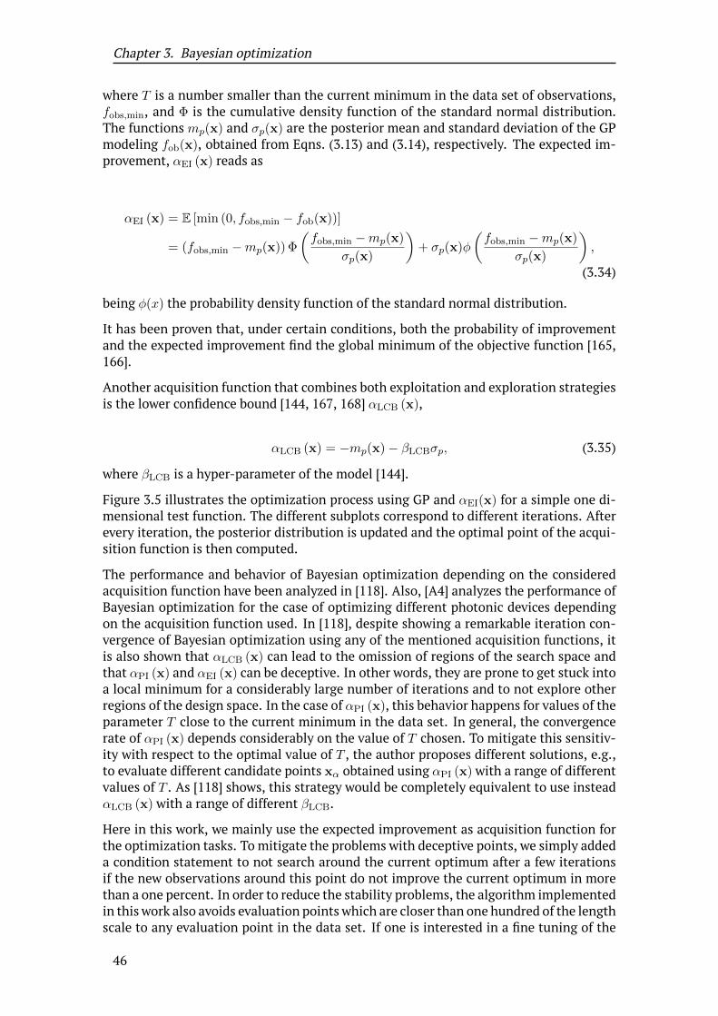
Chapter 3. Bayesian optimization
where T is a number smaller than the current minimum in the data set of observations,fobs,min, and Φ is the cumulative density function of the standard normal distribution.The functionsmp(x) and σp(x) are the posterior mean and standard deviation of the GPmodeling fob(x), obtained from Eqns. (3.13) and (3.14), respectively. The expected im-provement, αEI (x) reads as
αEI (x) = E [min (0, fobs,min − fob(x))]
= (fobs,min −mp(x)) Φ
(fobs,min −mp(x)
σp(x)
)+ σp(x)φ
(fobs,min −mp(x)
σp(x)
),
(3.34)
being φ(x) the probability density function of the standard normal distribution.
It has been proven that, under certain conditions, both the probability of improvementand the expected improvement find the global minimum of the objective function [165,166].
Another acquisition function that combines both exploitation and exploration strategiesis the lower confidence bound [144, 167, 168] αLCB (x),
αLCB (x) = −mp(x)− βLCBσp, (3.35)
where βLCB is a hyper-parameter of the model [144].
Figure 3.5 illustrates the optimization process using GP and αEI(x) for a simple one di-mensional test function. The different subplots correspond to different iterations. Afterevery iteration, the posterior distribution is updated and the optimal point of the acqui-sition function is then computed.
The performance and behavior of Bayesian optimization depending on the consideredacquisition function have been analyzed in [118]. Also, [A4] analyzes the performance ofBayesian optimization for the case of optimizing different photonic devices dependingon the acquisition function used. In [118], despite showing a remarkable iteration con-vergence of Bayesian optimization using any of the mentioned acquisition functions, itis also shown that αLCB (x) can lead to the omission of regions of the search space andthat αPI (x) and αEI (x) can be deceptive. In other words, they are prone to get stuck intoa local minimum for a considerably large number of iterations and to not explore otherregions of the design space. In the case of αPI (x), this behavior happens for values of theparameter T close to the current minimum in the data set. In general, the convergencerate of αPI (x) depends considerably on the value of T chosen. To mitigate this sensitiv-ity with respect to the optimal value of T , the author proposes different solutions, e.g.,to evaluate different candidate points xα obtained using αPI (x) with a range of differentvalues of T . As [118] shows, this strategy would be completely equivalent to use insteadαLCB (x) with a range of different βLCB.
Here in this work, we mainly use the expected improvement as acquisition function forthe optimization tasks. To mitigate the problems with deceptive points, we simply addeda condition statement to not search around the current optimum after a few iterationsif the new observations around this point do not improve the current optimum in morethan a one percent. In order to reduce the stability problems, the algorithm implementedin this work also avoids evaluation points which are closer than one hundred of the lengthscale to any evaluation point in the data set. If one is interested in a fine tuning of the
46

3.3. Bayesian Optimization Using Gaussian Processes
0
20f o
b
0
20
f ob
0
20
f ob
0.0
0.2
αEI
05
αEI
0
1
αEI
0
20
f ob
0
20f o
b
0
20
f ob
−1 0 1x
0.000.25 α
EI
−1 0 1x
0.0
0.1
αEI
−1 0 1x
0.0
0.1
αEI
Figure 3.5: Optimization process using a GP and the expected im-provement. After every evaluation of fob(x), the GP model is up-dated. The expected improvement is computed using the updatedGP posterior distribution and a new evaluation is calculated in thepoint with the highest expected improvement. The dashed lineshows the function fob(x) aimed to optimize.
global optimum, one can always run a gradient descent search using the global minimumfound by Bayesian optimization as starting point.
As described, the Bayesian optimization algorithm implies to solve another global opti-mizationproblemwithin each iteration, Eqn. (3.32). In principle, thismethodologymightseem to produce a large penalty in the efficiency of the algorithm with respect to manyother global optimization algorithms where the computation overhead can be negligible.Indeed, this is correct for a wide range of objective functions for which evaluations timesare shorter than a second. However, let us note that this work focuses on the optimizationof expensive objective functions that depend on the solution of Maxwell’s equations. Inthese problems, where one can not run the optimization for more than a few thousandsof iterations at maximum, the prediction power of Gaussian processes compensates thecomputation time overhead required in each iteration. This behavior has been analyzedin [A1], where Bayesian optimization was benchmarked with respect to a series of differ-ent global and local optimization algorithms in the optimization of a variety of differentphotonic devices. The results shown there confirm Bayesian optimization with Gaussianprocesses to be an efficient tool for design of photonic devices.
Bayesian Optimization using derivative information
Section 2.3 presented the calculation of shape andmaterial derivatives of photonic struc-tures using the finite element method. Having access to the gradient of the objectivefunction with respect to the design parameters offers a better knowledge of fob(x)which,if used efficiently, should lead to a better convergence rate in its optimization.
47

Chapter 3. Bayesian optimization
Themost usedmethods to exploit the gradients of fob(x) for its optimization are the gra-dient descendentmethods or quasi-Newtonmethods such as L-BFGS-B [169–171]. Thosemethods are used to find a local optimum of fob(x). The direction given by the gradientor the gradient and Hessian, in the case of quasi-Newton methods, ensures that the lo-cal optimum can be found. The mentioned methods are commonly used for the design ofmultiple types of photonic devices, especially in the field of topology optimization, wherelocally optimized devices show good performances [25, 27, 87, 88, 172–174].
In the context of global optimization, the use of derivative information is not as commonas for local optimization. There are not many algorithms that can exploit the deriva-tives efficiently. The most frequently used strategy consists in applying a gradient de-scendent method at different initial points within the design space to find multiple localminima [175].
Because Gaussian processes can easily incorporate derivative information, Bayesian op-timization provides an alternative to multi-start gradient descendent. Once the poste-rior distribution conditioned on values of fob(x) and its derivatives is obtained, see sec-tion 3.2, the same procedure as for the case without derivative observations applies toperform Bayesian optimization. Figure 3.6 shows the optimization process of the sameone dimensional test function as already presented in Fig. 3.5 when the Gaussian processincludes also derivative information. As it can be seen, the optimization finds the globalminimum faster than for the case without derivative observations.
0
20
f ob
0
20
f ob
0
20
f ob
0
10
αEI
0.0
0.5
αEI
0.0
0.2
αEI
0
20
f ob
0
20
f ob
0
20
f ob
−1 0 1x
0.000
0.005
αEI
−1 0 1x
0.0000
0.0005
αEI
−1 0 1x
0.0
2.5
αEI
×10−8
Figure 3.6: Example of Bayesian optimization using Gaussian pro-cesses with observations of the derivative and the use of the ex-pected improvement as acquisition function. The objective func-tion used as example is the same as used in Fig. 3.5. Note how thealgorithm converges faster to the global minimum at x = 0 whencompared to the case where derivative observations were not in-cluded, i.e. Fig. 3.5.
Gaussian processeswith derivative information have been used in the context of Bayesian
48

3.4. Scalable Bayesian Optimization
optimization in [A1, A2, 161, 176]. The improvement in the convergence rate of the op-timization with respect to the algorithm without derivative observations depends on thebehavior of the objective function, as it can be seen in [A1]. There, Bayesian optimizationwith derivative information has been used to optimize different photonic devices and itsperformance was compared against Bayesian optimization without derivative informa-tion. The algorithm using derivative information shows a better performance for all thetest cases, although it can be seen how the difference in the convergence rate betweenboth algorithms is strongly influenced by the specific test case.
3.4 Scalable Bayesian Optimization
The scalability problem
Bayesian optimization shows excellent performance in terms of convergence. However,its use is generally limited to the optimization of problems with objective functions thatare expensive to evaluate. The reason for that is the poor scalability of Gaussian pro-cesses with the number of observations. Every time a new observation is added to themodel, the size of the covariancematrixKobs increases with an extra row and column. Toinfer the behavior of fob(x), one needs to calculate the Cholesky decomposition ofKobs,Eqn. (3.16), and then one needs to perform a forwards and a backward substitution for thedifferent pointsx. The number of operations to calculate the Cholesky decomposition re-quiresO(N3
obs) operations and every forward and backward substitution requiresO(N2obs)
operations. The scaling in time is directly proportional to the scaling in the number ofoperations.
The poor scaling of Bayesian optimization is not a major problem for the optimizationof many photonic devices, as the computational costs of computing the objective func-tion are generally high, already limiting the number of evaluations that one can per-form. However, there are other applications of interest where one can solve the objectivefunction in a few seconds. This is the case, for example, for highly symmetric photonicdevices, where one can use the symmetries to reduce the computational costs, or in sit-uations where one can perform many evaluations of the objective function in parallel.Therefore, reducing the effective time per simulation. In these cases, it is possible toperform thousands of simulations within a few days and there, the scalability of Gaus-sian processes become a major limiting factor of the optimization process.
Figure 3.7 shows the time needed to perform the Cholesky decomposition and the sin-gular value decomposition ofKobs as a function of the number of evaluations Nev of theobjective function, i.e., the number of times that one calculates the objective functionat different points of the design space. As one can see, the time follows a third-orderpower law with respect to the number of evaluations for both methods. The poor scalingbecomes a major limiting factor especially when one can obtain derivative informationvia the direct or the adjoint method. In this case, one gets 1+d observations with eachevaluation. That is to say, with the addition of d derivative observations per simulation,the number of observations, which lead to new extra rows and columns in the covariancematrix, equals (1 + d)Nev. This is visible in Fig. 3.7, which also shows the time requiredto perform the Cholesky decomposition after every evaluation of the objective functionwhen the derivative observations of 10 parameters are included. As one can see, afterthree thousand simulations, decomposing Kobs already takes a few tens of seconds. Togive an idea, computing ten thousand simulations of many two dimensional models withthe finite element method is a task that can be done in a few hours exploiting paralleliza-tion. We have already discussed how the use of derivative information in Bayesian opti-
49

Chapter 3. Bayesian optimization
mization is, in principle, beneficial, as it allows to obtain even better convergence rates.However, because of the scalability problems, the use of derivative information may notbe beneficial in some of the cases when one has access to tens of thousans of evaluta-tions and the derivatives do not improve the convergence rate significantly. Knowing inadvance to which of the problems this applies is a non-trivial task.
103 104 105
Number of evalulations (Nev)
10−3
10−1
101
103
105
Calcu
lation
time(s)
svd Kobs (fob) LKobs(fob) LKobs
(fob, dfob/dxi)
10−12 ·N3ev
113 · 10−12 ·N3ev
Figure 3.7: Time needed to perform the Cholesky decompositionof the covariance matrixKobs for a problem with d = 10 parameters.The results are shown for the the case where only observations offob(x) are included (orange dots) and for the case when one gets ob-servations of the derivatives of fob(x) respect to 10 parameters witheach evaluation (green dots). The plot shows also the time neededfor computing the singular value decomposition (SVD) ofKobs (bluedots).
In addition to the decomposition of Kobs, it is also necessary to perform a forward anda backward substitution to infer the standard deviation at a point in the design space,Eqn. (3.16). Although the time required to perform this operation is much shorter thanthe time required to compute LKobs
, this operation is required multiple times during theoptimization of the acquisition function, Eqn. (3.32). One technique that we use to mit-igate this issue is to use optimization methods for the acquisition that evaluate the ac-quisition function at many points in parallel. With this approach, one can reduce thetimes for accessing the memory to read the entries of LKobs
. Another method proposed,and that it is also used in this work, consists in obtaining the next evaluation point at thesame time the objective function is solved [A1, 135, 177].
Below we present two different methods to mitigate the scalability problems of Bayesianoptimization and we discuss about their performance. Both methods are still based onGaussian processes as the surrogate model. The first method exploits a specific numer-ical scheme on the matrix update of the Cholesky decomposition of Kobs. This methodreduces the scalability problem from O(N3
obs) to O(N2obs) without the need to use any
approximation with respect to the standard Bayesian optimization method. The sec-ond method is similar to the method proposed in [152]. It is based on the use of a lo-
50

3.4. Scalable Bayesian Optimization
cal Bayesian optimization model and a data structure to efficiently generate the localmodel. However, unlike [152], in the method proposed here the local model is not fixedand it evolves with the candidate point x∗. In the following subsections each of theseapproaches are described.
Matrix update of the Cholesky decomposition
Let us start describing the first proposed method. It is based on the work that we pre-sented in [A2]. In the suggested approach with use of derivative information, we updatethe Gaussian process model with a new set of d + 1 observations. These observationslead to d+ 1 extra rows and columns that are added to the covariance matrix. Then, theCholesky decomposition of the covariance matrix needs to be re-calculated. However,the Cholesky decomposition of a major block of the covariance matrix was already com-puted in the previous iteration of the Bayesian optimization algorithm. If we split thecovariance matrix into four blocks,
Kobs =
[A BT
B C
], (3.36)
the Cholesky decomposition of Kobs can be described in terms of the four blocks. Here,A represents the covariance matrix computed in the previous iteration of the Bayesianoptimization algorithm.
The covariance matrix ofKobs, LKobs, can be obtained in terms of the blocks A, B and C
as ([178] section 6.5.4)
LKobs=
[LA 0
B · L−TA LS
], (3.37)
with S being the Schur complement ofKobs,
S = C −B ·A−1 ·BT . (3.38)
The second term of the above expression can be written as a vector-vector multiplica-tion,
S = C −X ·XT . (3.39)
For that, we used the equality between the Cholesky decomposition of the inverse of amatrix and the inverse transpose of the Cholesky decomposition of the matrix,
M = LM · LTM , (3.40)
M−1 = L−TM · L−1M , (3.41)
M−1 = LM−1 · LTM−1 , (3.42)
LM−1 · LTM−1 = L−TM · L−1M . (3.43)
XT can be obtained solving the triangular system LA ·XT = BT .Finally, one gets the aimed expression,
51

Chapter 3. Bayesian optimization
LKobs=
[LA 0X LS
]. (3.44)
101 102 103 104
Number of evaluations (Nev)
10−4
10−2
100
102
104
Calcu
lation
time(s)
LKobs(fob, dfob/dxi)
LKobs(fob, dfob/dxi) mat. update
113 · 10−12 ·N3ev [s]
5 · 113 · 10−11 ·N2ev [s]
Figure 3.8: Time needed to perform the Cholesky decompositionof the covariance matrixKobs for a problem with d = 10 parameterscomputing the full Cholesky decomposition (green dots) and usingthe matrix update scheme (red dots). The results are shown for thecase where observations of the derivatives of fob respect to the 10parameters are included into the GP model.
The numerical implementation of the matrix update scheme that we made is based ona C implementation of the BLAS [179] and LAPACK [180] libraries. Figure 3.8 shows thecalculation times required to compute the Cholesky decomposition of Kobs as a func-tion of the number of evaluations, using the matrix update scheme. As in Fig. 3.7, theresults are shown for the case of adding the observation of fob(x) and for the case ofadding also the derivatives dfob(x)/dxi for 10 different parameters. As it can be seen, thenew scheme scales with O(N2
obs) instead of with O(N3obs). For example, calculating the
Cholesky decomposition after 10 thousand evaluationswith derivative observations of 10parameters requires 5 seconds using thematrix update scheme. The standard scheme re-quires one and a half minutes, as shown in Fig. 3.7. Note that the use of thematrix updatescheme does not imply any approximation of the standard Bayesian optimization tech-nique. Therefore, it keeps the same convergence properties as the standard algorithm,provided that the matrix update does not introduce numerical errors. The stability of themethod will be discussed below.
52

3.4. Scalable Bayesian Optimization
Stability of Gaussian processes
We have just described a technique to reduce the scaling of Bayesian optimization fromO(N3
obs) toO(N2obs). Themethod does not rely on any approximation but on the exploita-
tion of the information that one already has about the Cholesky decomposition of thecovariance matrix from previous iterations. This fact implies that the convergence opti-mization rate of the method is the same as of the standard Bayesian optimization, if onecan show that the numerical procedure does not add extra numerical errors when per-forming the inference. This is a fair question especially in Bayesian optimization, as it isknown that the covariance matrix becomes increasingly ill-conditioned with the numberof iterations, especially upon incorporation derivative observations [176].
To mitigate the numerical errors produced by the ill-conditioned covariance matrix, dif-ferent regularization techniques have been proposed [155]. The most frequently usedmethods are the use of the Cholesky decomposition ([125] section 2.2), the truncatedsingular value decomposition [181] (TSVD) or the use of the LU decomposition ([182]section 3.1.1). The TSVD is the most flexible method, in the sense that one has morecontrol over the error that the algorithm introduces. However, the Cholesky decomposi-tion is usually preferred in many implementations, as it is the fastest method among thethree mentioned above and shows simultaneously a good stability. The Cholesky decom-position and the LU decomposition require in the order of 1/3 N3
obs and 2/3 N3obs floating
point operations respectively ([84] section 23) and the first phase of the SVD, generallythe most expensive part of the algorithm, requires 8/3 N3
obs floating point operations ifone uses the Golub-Kahan bidiagonalization ([84] section 31).
To see if thematrix update scheme introduces significant errors in the posterior Gaussianprocessmodel, themethod is comparedwith other differentmethods used to perform theinference of the Gaussian process model: the Cholesky decomposition of the covariancematrix, the truncated singular value decomposition, and the direct inversion of the co-variance matrix. The comparison measures the error produced by the different methodsin the value of σp at all the observation points of a data set obtained during the Bayesianoptimization of an objective function. The error assigned to eachmethod is themaximumerror in σp obtained from all the observation points. Note that in an error free method,σp should be zero at all the observation points. The results are shown in Fig. 3.9.
The results for the direct inversion show how the error of the model explodes when noregularization method is used. This clearly indicates that the use of some regularizationtechnique is in fact needed. The error of the truncated singular value decompositionfollows the same behavior of the direct inversion until it reaches an error of around 10−9.The reason for that is the cutoff limit imposed for the singular values. The inverse of thesingular values was set to zero to all singular values obtained lower than 10−9. However,the most important result of the comparison is the confirmation that the matrix updatescheme remains stable and that the error produced by it is as low as the error produced bythe full Cholesky decomposition. The reason behind this result could be explained by thefact that the algorithm for the Cholesky decomposition also builds thematrix row-by-rowor column-by-column without pivoting [178].
In addition to thematrix update of the Cholesky decomposition, in [A2] we also proposedand analyze the use of a matrix update scheme for the inverse of the Cholesky decom-position. This scheme would allow to make the inference twice faster than with the useof the Cholesky decomposition. However, the results that we present there show that, incontrast to the Cholesky decomposition, the method is unstable.
53

Chapter 3. Bayesian optimization
101 102 103 104
Size of Kobs
10−14
10−11
10−8
10−5
10−2
Errorinσp
Direct inversion
TSVD
Cholesky
Cholesky (mat. update)
Figure 3.9: Error produced for the inference ofKobs using differenttechniques to solve the linear system of Eqn. (3.14): the Choleskydecompoisition, the matrix update of the Cholesky decomposition,and the singular value decomposition.
Bayesian optimization with a local Gaussian process model
The secondproposedmethod to improve the scalability of the Bayesian optimization con-sists in the use of anupdated local Gaussian processmodel that contains amaximumfixednumber of observations. For a given point x∗ where the value of the acquisition functionis needed, the algorithm generates a posterior distribution based on a Gaussian processmodel that uses only a subset with the nearest Nnearest observations of the data set. Thereason to explain why a local GPmodel can work is related to the exponential behavior ofthe covariance functions generally used, see Eqns. (3.6)-(3.10). The further away a pointof the data set is from the pointx∗, the less correlated are their values, and the correlationfactor contains an exponential decaying factor with the distance between the two points.Therefore, the estimation values for x∗ will not be strongly influenced by the points fur-ther away in the data set. A different strategy to the use of a fixed numberNnearest can beto use only the points for which the correlation value with x∗ is lower than 1/(100∆fob),being ∆fob the maximum difference between the different values of the objective valuein the data set of observations.
Given the point x∗, the first step of the algorithm consists in determining which of theNobs observations are the nearest neighbours to this point x∗. There aremany algorithmsto efficiently determine the nearest neighbors, as the k-d tree algorithm [183–185], thecover tree algorithm [186, 187], the R-tree [188–190] or uniform grid cell structures [191,192]. Here, we use a grid-R-tree [193] algorithm. The design space is divided into hyper-cubes whose side lengths equal to half the length scales of the hyper-parameters, li. A liststores the indices of the cells that are populated with at least one observation point. Thelist also contains their population number and it is updated with each new observationobtained. With this structure, the search for the nearest neighbours can be done in asub-linear time with respect to Nobs.
Once the subset of observations is chosen, the posterior Gaussian process is calculated.Note that this requires the calculation of the covariance matrix and its Cholesky decom-position to perform the inference, needed for the calculation of the acquisition func-tion.
54

3.4. Scalable Bayesian Optimization
To not recompute the covariance function and the Cholesky decomposition too often, asthe optimization for the acquisition function continues sampling at different points x∗,the subset for the local Gaussian process is not continuously updated. It only updateswhen more than a γupdate percentage of the closest neighbours for the current x∗ is notcontained in the subset used the last time that the covariance matrix was computed. Inpractice, if one uses a gradient descendent algorithm to optimize the acquisition func-tion, the update is required a few times atmaximum for each starting point of the gradientdescendent. The tests of the implementation show that the posterior Gaussian process,when used in combination with a gradient descendent strategy for the optimization ofthe acquisition function, needs to be updated in average once every 10 evaluations of theacquisition function. This number has been obtained for a Nnearest value of 300 and aγupdate of 15%.
With this implementation, the scaling of the method is sublinear once the number of to-tal observationsNobs exceedsNnearest and if the algorithm does not increase the numberof starting points for the optimization of the acquisition function with the number oftotal observations Nobs. However, there are two main fundamental questions that needto be answered. The first one is how much time the algorithm requires per observation,and if this time is actually lower than the average time required by the standard imple-mentation of Bayesian optimization in practical applications. Although the algorithmdoes not scale with the number of observations, at least in a certain range after Nobs ex-ceedsNnearest, the proposedmethodmust be slower than the standard implementation ofBayesian optimization, as different covariancematrices and their respective Cholesky de-compositionsmust be computed. The second important aspect that needs to be answeredis how the convergence rate of the algorithm performs with respect to the standard ap-proach. The use of a local surrogate model implies that not all the available informationis accessible for each candidate x∗ and how this affects the convergence of the methodmust be measured.
To obtain an approximate idea for these two aspects, the performance of the method iscomparedwith respect to the standard implementation of Bayesian optimization for a se-ries of optimization runs of a test function. The comparison consists in the optimizationof the Rastrigin function [194, 195] in a parameter space of five dimensions,
fRastrigin = 50 +5∑
i=1
x2i − 10 cos (2πxi), (3.45)
and for a design space bounded by |xi| ≤ 10. The Rastrigin function has a global optimumof fRastrigin(xopt) = 0 at the point xopt = [0,0,0,0,0]. Within the design space considered,the function contains around 4 million local minima.
The optimization is performed four different times for both algorithms. The optimiza-tions run until they reach three thousand iterations. All the different aspects of the op-timization algorithm, as the number of starting points used for the acquisition function,the criteria for choosing the starting points for the local optimizations, etc. are identicalfor the two algorithms. Also the length scales are kept fixed in bothmethods, with a valueof li = 0.7 for all the dimensions. To optimize the acquisition function both algorithmsrun twenty local optimizations using the L-BFGS-B algorithm [169, 171]. For this test, thelocal optimizations are run sequentially. Both algorithms include also the observationsof the derivatives of the test function.
The results for the optimization convergencewith respect to the number of evaluations offRastrigin(x) are shown in Fig. 3.10 for both methods, the standard Bayesian optimization
55

Chapter 3. Bayesian optimization
and the local approximation proposed here. The results shown correspond to the averageresults of the four different runs for each of the two methods. As one can see, for thisparticular test and implementation of both algorithms, the standard algorithm showsa slightly better convergence, although the differences are within the σ bands of bothalgorithms.
0 500 1000 1500 2000 2500 3000
Iteration
101
102
Avg.cu
rrentminium
standard
local
Figure 3.10: Comparison of the convergence of the two differentBayesian optimization algorithms with respect to the number ofevaluations of the objective function. The results are shown fora standard Bayesian optimization algorithm and for the local ap-proximation proposed in this work. The objective function to beoptimized is the Rastrigin function in five dimensions, shown inEqn. (3.45). Every iteration corresponds to the addition of one ob-servation of the objective function and of its derivatives with re-spect to each input parameter. The results shown for each of thealgorithms are the average of four different optimization runs. Theshadowed area indicates the region within one standard deviationof the multiple runs performed.
Figure 3.11 shows the averaged computation time required by the last 50 iterations asa function of the iteration number. There, one can see how the time required by thelocal approach does not scale. Note that the times required by the standard Bayesianoptimization algorithm are generally smaller than the ones shown in Fig. 3.11, as onewould normally run the optimizations for the expected improvement in parallel and notsequentially. However, the scaling would still be similar and the difference with respectto the results of Fig. 3.11 would be a constant scaling factor.
Although with the method proposed in the previous section one can already efficientlycover most of the applications of interest in the design of photonic nanostructures with-out theneed to use any approximation, altogether, the results obtained seem topoint thatthe proposed use of local Gaussian processes can be a promising substitute of the stan-dard Bayesian optimization for problems with moderately fast objective functions. Also,the use of local Gaussian processes results in a highly parallelizable method, since thememory usage per local Gaussian process is low. Further research on this method couldalso analyze the impact of optimizing the hyperparameters for each of the local Gaussianprocess in the optimization convergence and in the computational overhead.
56

3.5. Conclusions
0 500 1000 1500 2000 2500 3000
Iteration
0
100
200
300
400
Avg.
timeper
iteration(s)
standard
local
Figure 3.11: Time per evaluation required by a standard Bayesianoptimization algorithm and the scalable proposed algorithm to ob-tain the next point where to evaluate the objective function. Theobjective function to be optimized is the Rastrigin function in fivedimensions, shown in Eqn. (3.45). Both algorithms include deriva-tive observations with respect to the five input parameters.
3.5 Conclusions
This chapter proposes and describes an implementation of Bayesian optimization for theglobal optimization of nanophotonic devices. The use of Gaussian processes as stochas-tic model provides a method able to incorporate both the objective value and its deriva-tives obtained from the finite element solver, which offers high predictive capabilities.These factors translate in an optimization method with a good iteration convergence, asit has been shown in several benchmarks. Furthermore, the chapter proposes two differ-ent techniques to improve the scalability issues of Bayesian optimization. These meth-ods extend the efficient usage of Gaussian processes into a wider range of optimizationproblems for photonic applications.
The optimization methods presented here are the fundamental tool used in the nextchapters of the thesis for the design of photonic structures. Specially in chapter 5, wherewe present the design of photonic structures used for different applications.
Once explained the optimization method developed for the optimization of photonicstructures, in the next chapter we present some numerical tools to analyze and optimizeisolated scatterers and the structures obtained from these elements, e.g., metasurfaces.Finally, chapter 5 combines the use of Bayesian optimization and the tools presented inchapter 4 to show, with some examples of design of photonic structures, the relevance ofthe developed tools.
57


4 | Design of isolated scatterers
4.1 Introduction
Among the multiple types of photonic devices used to manipulate and control light,there is a wide range of them that are either entirely or in part composed of isolatedscatterers embedded in a homogeneous medium. Examples of these kind of devices arenano-antennas [196–200], devices used to promote the interaction of light [201–203],and metamaterials in general [204–207]. Here, arrangements made from a larger num-ber of small scatterers are used to create artificial photonic materials capable of con-trolling light propagation in manners inaccessible with homogeneous natural materials.Further devices that are made from ensembles of scatterers are metalenses that can beused for different applications [208–210] or photonic crystals with spatially dependentproperties [211]. Ensembles of many scattering particles also find use in layers that offerlonger effective photon path lengths to improve absorption in thin-film solar cells [212]or as chiral metamaterials that can act as a direction independent circular polarizationfilters [213]. In all these examples for possible devices, the position, shape, andmaterialsof the scatterers are design parameters, which one can optimize for the desired applica-tion. The purpose of this chapter is to describe a strategy to design isolated scatterersaccording to a predefined purpose. That requires to describe the interaction of light withsuch a scatterer at first.
One very well established tool to study the interaction of a given scatterer with a givenillumination bases on themultipole expansion. There, the scattered field from the objectis expanded in frequency domain into a basis of radiative vector spherical wave functions,VSWFs,
Escat(r) =
∞∑
n=1
n∑
m=−n
[am,nN
(3)m,n (r) + bm,nM
(3)m,n (r)
]. (4.1)
The fieldsN (3)m,n (r) andM (3)
m,n (r) are the electric andmagnetic VSWFs, respectively. Theirdefinition and properties are presented in section 2.2. The complex coefficients am,n andbm,n capture the contribution of the respective multipoles to the scattered field. The de-composition shown in Eqn. (4.1) is valid everywhere outside the smallest sphere circum-scribing the scatterer. There is not yet a proof about the validity of the decompositionin the region inside the sphere. The assumption that the expression is valid inside thesphere is known as the Rayleight hypothesis [214–216].
In addition to the valuable information that themultipole expansion directly provides forstudying and designing scatterers, the multipole expansion is also an important ingredi-ent to construct the T-matrix of a given object [42, 217, 218]. The T-matrix of an objectprovides the field scattered by any field illuminating the object. The T-marix expresseshow an incident field, expanded into a series of incident VSWFs, is scattered into a set of
59

Chapter 4. Design of isolated scatterers
outgoing VSWFs. With that it contains all the information about how an object interactwith light; it is the most comprehensive representation of the object concerning its opti-cal properties. The T-matrix can be used to obtain different quantities, such as the totalinteraction cross section of a scatterer with light, the absorption of the object under acertain illumination ([42] section 5.1) or the duality of the object or its electromagneticchirality [213]. However, the T-matrix is also important to calculate the optical responsefrom clusters that consist of a large numbers of scatterers [219, 220]. When solving thismultiple scattering problem, the scatterers themselves are represented only on the baseof their T-matrix. Current computational resources allow for clusters with half a millionscatterers to be solved numerically [A5].
There are different numerical methods for calculating the T-matrix of an object. Thevalidity and efficiency of each method depends on the symmetries of the object and itsmaterial and geometrical complexity. For example, the T-matrix of a sphere can be ob-tained analytically using Mie theory [62, 63]. For homogeneous scatterers, composed ofonly one material, but with geometries different than a sphere, the extended boundaryconditionmethod (see, e.g., [217, 221] or [42] section 5.8) is an efficientmethod for calcu-lating the T-matrix. However, thismethod is only valid for objects homotopic to a sphere.To compute the T-matrix of objects composed of multiple materials and with more com-plex geometries, a more general method for solving Maxwell’s equations is needed. Thefinite element method is especially suitable for dealing with complex geometries. Here,the procedure to compute the T-matrix of an object consists of two main steps. In a firststep, the finite element method is used to solve the scattered fields, Escat, for a set ofdifferent illuminations. In a second step, the scattered fields are expanded into the basisof VSWF. For that, one uses the orthogonal properties of the VSWF, Eqns. (2.44)-(2.44),and the complex expansion coefficients of the scatttered field are calculated as
am,n =
∫S2RN
(3)∗m,n (r) ·Escat (r) dS
∫S2R|N(3)
m,n (r) |2 dS, (4.2)
bm,n =
∫S2RM
(3)∗m,n (r) ·Escat (r) dS
∫S2R|M(3)
m,n (r) |2 dS. (4.3)
The elements am,n and bm,n of the multipole decomposition either directly correspond toentries of the T-matrix, if one uses regular VSWFs as illuminations, or an intermediatelinear system has to be solved to link the values am,n and bm,n with the entries of theT-matrix. This last procedure is needed in the case that another type of illuminations isused, as for example plane waves [222].
In Eqns. (4.2) and (4.3), the decomposition is obtained as a series of surface integralsacross the boundary of a sphere circumscribing the scatterer, SR. The fact that this sur-face has to be a sphere presents some drawbacks. To perform the integral, the scatteredfield has to be interpolated across the surface of the sphere. The interpolation suffersfrom accuracy losses and it also makes the calculation computationally more expensiveand, therefore, slower. One possible solution to this drawback consists of performing thedecomposition based on volume integrals of the induced currents in the object [205, 223,224]. In this chapter, another method is presented, extending the orthogonality prop-erty of the VSWFs to surfaces with general shapes. This contribution has been discussedin [A6]. With such a generalization, one can use the boundaries of the computational do-main or the boundary of the scatterer to perform the decomposition. Computing surfaceintegrals over these natural surfaces is not only easier, but also frequently more efficient.
60

4.2. Decomposition of scattered fields into VSWFs using surfaces with general shapes
Most numerical solvers for Maxwell’s equations already provide efficient methods to ac-curately compute surface integrals over these boundaries for quantities dependent onthe scattered field. For similar reasons, if the numerical solver provides shape and mate-rial derivatives for similar surface integrals, such as the integral of the Poyinging vector,they can be easily modified to obtain the shape and material derivatives of the multipoledecomposition. This allows for the computation of the derivatives of T-matrices of gen-eral complex scatterers, enabling the efficient optimization of such scatterers. The shapederivatives can be used for the optimization of a single scatterer or for the optimizationof multiple scatterers in amore complex system, combining themulti-scatteringmethodwith the adjoint method [225]. The next chapter presents one relevant example of designof an isolated chiral scatterer where one can benefit from these developments.
This chapter is devoted to the description of different methods related to the multipoledecomposition, used to analyze and design single scatterers or clusters of them. The firstsection presents the derivation of the mutlipole decomposition using surfaces of generalshapes. After that, its numerical implementation is outlined using the finite elementmethod. An extra section is used to present the implementation for the specific caseof cylindrically symmetric objects. Cylindrically symmetric scatteres are widely used inmany different applications and this implementation drastically reduces the computa-tional time and resources with respect to the more general implementation. A fourthsection describes a proposed method to compute the T-matrix of complex objects. Af-ter that, the implementation of the calculation for shape and material derivatives of theT-matrix is presented. Finally, the last section describes an implementation of the ad-joint method for multi-scattering problems based on the T-matrix method and the shapederivatives of the T-matrix.
Most of the numerical tools presented in this chapter will be used in the following chap-ter for designing maximal em-chiral scatterers. These scatterers show considerable dif-ferences in their interaction strength with plane waves of different circular polarizationhandedness and for multiple illumination angles, which makes them interesting for dif-ferent applications.
4.2 Decomposition of scattered fields into VSWFs using sur-faces with general shapes
Mathematical derivation
This section derives the general orthogonality relation for VSWFs. This expression con-sists of an integral evaluation over a general closed surface that encloses the scatteringobject.
The derivation assumes that the scattering object is surroundedby ahomogeneous, isotropic,and lossless medium. To obtain the expression, we start by taking two vector fields thatare solutions of the same wave equation, Eqn. (2.23), Escat(r) and F(r). Escat(r) is thescattered field produced by the object under a certain illumination and F(r) is anotherfield that equally fulfills the Silver-Mueller radiation condition, Eqn. (2.50). The genericfield F(r) is used for simplicity, and only in the last step of the derivation it will be re-placed by the radiative VSWFs to obtain the final desired expression.
To obtain a scalar product between the two fields Escat (r) and Fscat (r), we start by mul-tiplying the wave equation for the field Escat (r) by the complex conjugate of F (r),
F∗ (r) · ∇ × (∇×Escat (r)) − k2F∗ (r) ·Escat (r) = 0. (4.4)
61

Chapter 4. Design of isolated scatterers
The above expression is then integrated over a volume V that surrounds the object butit shall not contain any source of the scattered field. To be specific, V denotes a closed re-gion that surrounds the object, butwhich does not contain it, as illustrated in Fig. 4.1,
∫
V
(F∗ (r) · ∇ × (∇×Escat (r)) − k2F∗ (r) ·Escat (r)
)dV = 0. (4.5)
V
Figure 4.1: Sketch of geometry considered in the derivation of themultipole expansion of scattered fields using surfaces with generalshapes. An object within a homogeneous background medium pro-duces a scattered field. Equation (4.5), which involves the radi-ated field, is integrated across a volume V that surrounds the objectwithout containing it. The volume is delimited by an inner bound-ary Γ1 and an outer boundary Γ2. At the end of the derivation, onlythe field across the boundary Γ1 is necessary to obtain the expan-sion.
We apply the generalized Stokes’ theorem [226] to Eqn. (4.5) twice to convert part of thevolume integral into a surface integral across the boundaries of V ,
0 =
∫
Γ(∇×Escat (r))× F∗ (r) · dS
+
∫
V
(∇×Escat (r)) · (∇× F∗ (r))− k2F∗ (r) ·Escat (r)
dV
=
∫
Γ(∇×Escat (r))× F∗ (r) + Escat (r)× (∇× F∗ (r)) · dS
+
∫
V
(Escat (r) · ∇ × (∇× F∗ (r)) − k2F∗ (r) ·Escat (r)
)dV
(4.6)
Using now the assumption that F (r) also fulfills the homogeneous wave equation, andtherefore also F∗ (r), the volume integral in Eqn. (4.6) vanishes and we obtain an expres-sion involving only a surface integral,
62

4.2. Decomposition of scattered fields into VSWFs using surfaces with general shapes
∫
Γ(∇×Escat (r))× F∗ (r)− (∇× F∗ (r))×Escat (r) · dS = 0. (4.7)
In the next step, we split the surface integral into the contributions of the inner surfaceΓ1 and the outer surface Γ2, see Fig. 4.1,
−∫
Γ1
(∇×Escat (r))× F∗ (r)− (∇× F∗ (r))×Escat (r) · dS
+
∫
Γ2
(∇×Escat (r))× F∗ (r)− (∇× F∗ (r))×Escat (r) · dS
= I1 + I2 = 0. (4.8)
The minus sign in the above expression comes from the definition used for the differ-ential surface elements, with dS pointing inwards the volume V on Γ1 and outwards onΓ2.
Up to this point, no restriction was imposed on the shape of the boundaries Γ1 or Γ2. Forthe remainder of this derivation, the outer surface Γ2 is assumed to be a sphere of radiusR, SR. Applying the circular shift theorem over I2 one gets,
I2 =
∫
S2R
(∇×Escat (r))×F∗ (r)·dS−(∇×F∗ (r))×Escat (r)·dS
=
∫
S2R
dS×(∇×Escat (r))·F∗ (r)−dS×(∇×F∗ (r))·Escat (r). (4.9)
We now assume that the radius R is large enough such that the far-field radiation condi-tion (2.50) is fulfilled,
limR→∞
(∇× Escat (r) ,F (r))×Rr = + limR→∞
ikR Escat (r) ,F (r). (4.10)
Expressing the differential surface element of the sphere in spherical coordinates,
dS = R2 sin θ dθ dφ r, (4.11)
we can integrate it into the far-field condition,
limR→∞
(∇× Escat (r) ,F (r))× dS = + limR→∞
ikdS Escat (r) ,F (r). (4.12)
Substituting this last expression into Eqn. (4.9) we obtain,
limR→∞
I2 = − limR→∞
ik
∫
S2R
(Escat (r) · F∗ (r) + F∗ (r) ·Escat (r)) dS. (4.13)
Finally, the generic field F is replaced by the radiative VSWFN(3)m,n (r) orM(3)
m,n (r),
63

Chapter 4. Design of isolated scatterers
∫
Γ1
(∇×Escat (r))× M,N(3)∗
m,n (r)
−(∇× M,N(3)∗
m,n (r))×Escat (r)
· dS
= limR→∞
2ik
∫
S2R
Escat (r) · M,N(3)∗m,n (r) dS.
(4.14)
If we compare the term on the right hand side of the above expression with Eqns. (4.2)-(4.3), we see that it equals the complex coefficients of the multipole expansion times thenorm of the VSWF at infinity, which is equal to 1
k ([42] Eqn. (C.152)),
∫
Γ1
(∇×Escat (r))× M,N(3)∗
m,n (r)
−(∇× M,N(3)∗
m,n (r))×Escat (r)
· dS
= a, bm,n 2ik limR→∞
∫
S2R
| M,N(3)m,n (r) |2 dS
= a, bm,n2i
k.
(4.15)
Therefore, we obtained an expression to calculate the expansion of the scattered fieldsinto VSWFs using integrals across a surface with a general shape,
am,n =k
2i
∫
Γ1
(∇×Escat (r))×M(3)∗
m,n (r)− kN(3)∗m,n (r)×Escat (r)
· dS. (4.16)
bm,n =k
2i
∫
Γ1
(∇×Escat (r))×N(3)∗
m,n (r)− kM(3)∗m,n (r)×Escat (r)
· dS. (4.17)
Equations (4.16)-(4.17) can be also obtained using Lemma 6.38 of [227], applying it toEscat (r) and the VSWF. They are the central result of this section.
Once the scattered field is known, these two equations allow us to calculate the coeffi-cients of itsmultipole decomposition over any surface enclosing the scatterer. This resultis particularly interesting for practical reasons, as one can directly apply the equationson the boundaries of the computational domain used to solve the scattered field.
Note that the surface Γ1 can contain points or can be completely embedded into the re-gion where the Rayleigh hypothesis may not hold true and still the expressions wouldbe valid. This can be seen in Eqn. (4.14), where Eqns. (4.16) and (4.17) are linked to thevalues of the decomposition of the scattered field in the far-field region.
To test the above expressions, we considered a test field, Etest (r), composed of differentVSWF terms with well defined amplitudes,
Etest (r) = (0.5 + 0.5i) M(3)0,1 (r) + 0.03N
(3)3,3 (r) , (4.18)
and calculate the decomposition of Etest(r) into a set of different VSWF. The decompo-sition is done using a cube of side length lcube centered at the origin as the surface of
64

4.2. Decomposition of scattered fields into VSWFs using surfaces with general shapes
integration. For the test, a non-adaptive trapezoidal integration method was used. Thenumber of grid points used for the numerical integration was 40,000 for each face of thecube. The results obtained for the expansion are shown in Fig. 4.2a as a function of thecube side length.
0 2000 4000
Lcube (λ)
10−15
10−10
10−5
100
Absolute
error
a
a3,3 b0,1 b−1,2 b0,10
0 2000 4000
Lcube (λ)
10−27
10−21
10−15
10−9
Absolute
error
b
Figure 4.2: Error in different terms of the multipole expansion of ascattered field. The scattered field is given by Eqn. (4.18). a. Decom-position using the radiative VSWF, Eqn. (4.16). b. Decompositionusing the regular VSWF, Eqns. (4.21)-(4.22).
As we can see, for a fixed number of integration grid points, the error of the expansionworsens the closer the boundaries of the integration surface are to the origin of the co-ordinates. The reason for that comes from the singular behavior of the radiative VSWFsat the origin. It causes numerical instabilities due to the finite precision of the digitalrepresentation of the numbers and due to the finite discretization used for the surfaceintegral.
One possible solution to reduce this problem and improve the stability of the methodcould be to check if the radiative VSWF can be replaced by the regular VSWF in Eqn (4.16).The regular VSWFs differ from the radiative ones only in their radial dependence and theydo not suffer from the singular behavior, so it is in principle reasonable to think that theymight fulfill a similar orthogonality expression.
To check this, we substitute F (r) withN(1)m,n (r) into Eqn. (4.8). An equivalent procedure
to the one done here for the fieldsN(1)m,n (r) can be done for the fieldsM(1)
m,n (r).
Using the fact that the regular VSWFs can be expressed as a combination of the radiativeVSWFs and the VSWFs of type 4,
N(1)m,n (r) =
N(3)m,n (r) + N
(4)m,n (r)
2, (4.19)
and that thefieldsN(4)m,n (r) fulfill an inwards Silver–Müller radiation condition, Eqn. (4.13)
now reads as,
65

Chapter 4. Design of isolated scatterers
limR→∞
I2 = limR→∞
−ik∫
S2R
(Escat (r) · N
(3)∗m,n (r) + N
(4)∗m,n (r)
2
+N
(3)∗m,n (r)−N
(4)∗m,n (r)
2·Escat (r)
)dS
= limR→∞
−ik∫
S2R
Escat (r) ·N(3)∗m,n (r) dS. (4.20)
Therefore, we obtain an expansion for the scattered field into the radiative VSWFs usingan expression that only involves the regular VSWFs,
am,n = −ik∫
Γ1
(∇×Escat (r))×N(1)∗
m,n (r)
− kM(1)∗m,n (r)×Escat (r)
· dS,
(4.21)
bm,n = −ik∫
Γ1
(∇×Escat (r))×M(1)∗
m,n (r)
− kN(1)∗m,n (r)×Escat (r)
· dS.
(4.22)
Equations (4.21) and (4.22) are equivalent to Eqn. 5.175 of [42], derived there on theboundary of the scatterer, and used in the context of the extended boundary conditionmethod.
To see if the change improves the numerical stability of the expansion, the same testas shown in Fig. 4.2a is now repeated using Eqns. (4.21)-(4.22). The results are shownin Fig. 4.2b. As we can see, the error in the expansion using the regular VSWFs doesnot exponentially increase with the reduction of the cube length and it remains stable.Therefore, Eqns. (4.21) and (4.22) are more suitable for a numerical implementation ofthemultipole decomposition. These are the expressionswewill finally use in our FEM im-plementation of themultipole decomposition, whichwe proceed to describe below.
FEM implementation of the decomposition
Having now checked the numerical suitability of the expressions, the next step is to im-plement them into the finite element solver.
Equations (4.21)-(4.22) have two terms, one that depends on the electric field and an-other that depends on its curl. As the electric field is expanded into a basis of polynomialfunctions of a certain degree, its curl will be given by an expansion of a lower polynomialdegree. That implies that the numerical accuracy of the term depending on the curl isworse than the one of the directly computed field.
To improve the accuracy of the solution, one technique frequently used is to convert thepart of the surface integral that contains the curl of the field into a volume integral,
66

4.2. Decomposition of scattered fields into VSWFs using surfaces with general shapes
∫
Γ1
F∗ (r)× (∇×Escat (r)) · dS =
∫
V1
((∇×Escat (r)) · (∇× F∗ (r))− k2F∗ (r) ·Escat (r)
)dV , (4.23)
where V1 is the volume contained by the surface Γ1. Note that this is not the same volumeas the volume V used in the derivation of Eqns. (4.2)-(4.3).
Actually, the numerical technique does not evaluate the volume integral over the entirevolume V1. It uses only the field of the FEMmesh elements that are part of the surface Γ1.This is done to not increase the computational cost of having to solve an integral over thewhole volume V1. In order to do that, a zero extension operator [228] is applied, to createa decaying continuation of the scattered field over Γ1 towards the interior of the volume.This technique is not specifically used for the decomposition given by Eqns. (4.21) and(4.22). It is a common technique used in the FEM for computing different surface inte-grals, as for example the surface integral of the Poynting vector. The numerical trick isautomatically applied by the solver JCMsuite [229].
To test the FEM implementation1, first we compute the expansion of the field scattered bya sphere when it is illuminated by a linearly polarized plane wave. The VSWF expansionof the scattered fields produced by a sphere is a well known solution [62, 63], which has ananalytical expression. Figure 4.3 shows the scattering cross section split into the contri-butions of the different multipoles for different frequencies of the illumination, obtainedusing both the FEM implementation and Mie theory. The link between the coefficientsof the multipole decomposition and the scattering cross section has been described insection 2.2. The details of the simulation are described in the caption of the figure. As itcan be seen, the results of the FEM solution match the analytical solution up to a certainnumerical precision.
To further ascertain the accuracy of the method, we perform a convergence test of theerror of the decomposition with respect to the side length of the mesh elements used inthe FEM discretization, hFEM. The results are shown in Fig. 4.4. As it can be seen, theerrors in the decomposition decrease with the decrease of the mesh side length. An ad-ditional line was included showing the values of 0.8 · 10−4·h2
FEM. This behavior coincideswith the behavior of the relative error of the decomposition for the magnetic hexapole.The relative errors of the different multipoles show similar power law behaviors. Theseresults are in agreement with the theoretical asymptotic FEM convergence behavior of hp
for the electromagnetic fields ([231] section 5.7).
As a second test, the total scattering cross section of a silver nanorod is computed for awavelength range between 250 nmand 2 µm. The nanorod ismodeled as an ellipsoid witha semi-major axis of 225 nm and a semi-minor axis of 37.5 nm. The major axis is parallelto the x-axis. The nanorod is illuminated with a linearly polarized plane wave with wavevector pointing in the -z-direction. The electric field is parallel to the x-axis.
To check the validity of the decomposition, the total scattering cross section as com-puted from the multipole coefficients, Eqn. (2.52), is compared with the value obtainedfrom the calculation of the total scattered power using the time averaged Poynting vector,〈S〉 (r),
1After implementing and testing the decomposition with JCMsuite using an external Pythonmodule, thedecomposition was then fully integrated into JCMsuite as an extra feature of the software package. This finalintegration was mainly done by Martin Hammerschmidt. My work in this integration process was to test itand to help in the identification of the sources of errors.
67

Chapter 4. Design of isolated scatterers
400 600 800 1000
λ (nm)
10−12
10−9
10−6
10−3
σscat(µm
2)
e. dip.m. dip.
e. qua.m. qua.
e. oct.m. oct.
e. hex.m. hex.
Mie
Figure 4.3: Multipole decomposition of the field scattered by a sil-ver sphere illuminated by a plane wave. The wave vector of theplane wave is oriented in the -z-direction. Its electric field is lin-early polarized in the x-direction with an amplitude of 1 V/m. Thesphere has a radius of 112.5 nm and its permittivity at each wave-length is interpolated from a database [230].
σscat =
∫S 〈S〉 (r) · dS
2Z20 |Ei|2
, (4.24)
with S being a surface surrounding a volume that contains the nanorod, Z0 the charac-teristic impedance of free space, and Ei the amplitude of the plane wave.
For this example, the expressions (4.21) and (4.22) for themultipole expansionwere eval-uated directly on the boundary of the nanorod. The decomposition is shown in Fig. 4.5.The results obtained from both methods are in good agreement with each other.
As it can be seen in the decomposition, the nanorod sustains a principle resonance at awavelength of 1225 nm. At this wavelength, most notably the electric dipole moment isresonantly excited. To be precise, the dipolemoment oriented along themajor axis of thenanorod is resonantly excited, corresponding to the vectorial orientation of the electricfield used to illuminate the nanorod. Symmetry reasons prevent any electrical dipolemoment oriented in a direction other than the x-axis from being excited. This can beseen in Fig. 4.6, which shows the contribution of the different components of the electricdipole moments in the Cartesian basis to the scattering cross section. The electric dipolemoments oriented along the Cartesian axis and the electric dipolemoments that producethe VSWF fieldsN3
m,1 (r) are related as
pxpypz
=
1√2
1 0 −1−i 0 −i0√
2 0
p−1
p0
p+1
. (4.25)
This dipolar behavior is visible in Fig. 4.7a, which shows the intensity of the electric field
68

4.2. Decomposition of scattered fields into VSWFs using surfaces with general shapes
10 15 20 25 30 35
hFEM (nm)
10−5
10−3
10−1Relativeerrorinσscat
e. dip.
m. dip.
e. qua.
m. qua.
e. oct.
m. oct.
e. hex.
m. hex.
α · h2FEM
Figure 4.4: Convergence study for the errors in the multipole de-composition of the fields scattered by a silver sphere as a functionof the FEM mesh side length in the surrounding medium, hFEM.The sphere is illuminated by a plane wave with a wavelength of λ0
= 450 nm. The wave vector of the plane wave is oriented in the -z-direction. Its electric field is linearly polarized in the x-direction.The sphere has a radius of 112.5. Themesh side length of the spherediscretization equals hFEM/|
√εsilver|, being εsilver the relative per-
mittivity of the sphere, εsphere = -6.81+0.28i.
on the surface of the nanorod and in the plane x-z-plane at y = 0, which contains themajor axis of the nanorod. As it can be seen in the figure, the field is strongly local-ized around the corners of the particle and it resembles the field profile produced by anideal electric dipole. Such strong field intensities are characteristic of rod-like metallicparticles due to plasmonic excitations [232–234]. When one of the two dimensions ofthe nanorod is much longer than the other two, a low-energy local surface polariton, issustain [235].
Antenna theory describes how an ideal half-wave dipole antenna, a thin wire made outof a perfect electric conductor, would present a resonance peak in the scattering crosssection for an illumination wavelength equals to two times the length of the wire [236].However, at optical and near infrared frequencies, particles made out of silver can notbe assumed to be perfect electric conductors. The incident radiation is not perfectly re-flected on the surface of the particle but it penetrates a certain thickness into the particle.The electromagnetic response becomes then governed by collective electron oscillations,called surface plasmons. This different behavior with respect to the predictions from an-tenna theory leads to a shift of the resonance towards longer wavelengths [237], as itcan be seen in the results of Fig. 4.6. However, one could still approximately predict theposition of the resonance for a thin wire using a scaling correction of the wavelengthpredicted by antenna theory [238, 239],
λeff = λ0k0
γ− 4R. (4.26)
69

Chapter 4. Design of isolated scatterers
500 1000 1500 2000
λ (nm)
10−10
10−7
10−4
10−1σscat(µm
2)
e. dip.m. dip.
e. qua.m. qua.
e. oct.m. oct.
σscat,total
σscat,total,〈S〉
Figure 4.5: Cross section of a nanorod calculated using two differ-entmethods: themultipole expansion and the integral of the powerflux of the scattered field. The nanorod is a silver ellipsoid with asemi-major axis of 225 nm and semi-minor axis of 37.5 nm. Themajor axis is oriented along the x-direction. The nanorod is illumi-nated with a plane wave with the wave vector parallel to the -z-axisand the electric field linearly polarized in the x-direction.
500 1000 1500 2000
λ (nm)
0.0
0.2
0.4
0.6
σscat(µm
2)
pxpy
pz
Figure 4.6: Electric dipole contributions to the scattering cross sec-tion of the nanorod described in Fig. 4.5 as a function of the wave-length. The contributions are shown in terms of the three Cartesiandipole moments. The peak in the scattering cross section is associ-ated to resonant the excitation of the dipolemoment oriented in thex-direction. Symmetry reasons prevent the excitation of any otherelectrical dipole moment.
In the above equation, λeff would be thewavelength of the resonance for a half-wavelengthantenna. In the case of the nanorod simulated here, that would be λeff = 900 nm, fourtimes the semi-major axes. λ0 is the wavelength at the resonance peak, k0 is the wave
70

4.2. Decomposition of scattered fields into VSWFs using surfaces with general shapes
number in free space, R is the radius of the wire and γ is the propagation constant of thesurface charge wave for the TM0 mode of a cylindrical wire. We compute the value of γfollowing [240]. Assuming a wire with a constant radius of 37.5 nm, one obtains that aneffective wavelength of 900 nm would correspond to an illumination wavelength of 1229nm. This value of the position of the resonance peak is in very good agreement with theresults shown in Fig. 4.6.
Metallic nanorods similar to the one analyzed here have been proposed as an importantcomponent of different sensor devices [241–244]. One of the reasons for that is the highsensitivity that they present in the spectral position of the plasmon resonance. A smallchange in the refractive index of the surrounding medium shifts the resonance of thescattering cross section considerably, allowing to measure minute changes in the refrac-tive index.
225 nm
x
za
100
101
|~ E|(
V m
)x
zb
−1
0
1
Re(E
x)
|~ E|
Figure 4.7: a. Amplitude of the electric field in close vicinity to thenanorod upon its illumination with a plane wave at a wavelengthof 1225 nm. Other properties of the illumination and the nanorodcorrespond to those described in the caption of Fig. 4.5. The figureshows the amplitude in the x-y-plane at y = 0. The amplitude of thefield in the surface of the nanorod with y ≤0 is superimposed ontothe values of the plane. b. Direction of the electric field in the x-z-plane at y = 0 along with the real part of the x-component of theelectric field.
Decomposition of fields scattered from cylindrically symmetric objects
The decomposition and the FEM implementation proposed in the previous section is ageneralmethod that can be usedwith any structure, entirely independent on its complex-ity. On the other hand, there are different techniques to obtain the multipole expansion
71

Chapter 4. Design of isolated scatterers
for simple objects in a more efficient manner. A typical example would be the case of Mietheory for spheres and the extended boundary condition method applicable for homoge-neous scatterers that are homotopic to a sphere.
In a similar manner, the decomposition using the FEM can also be simplified if the scat-tering object has specific symmetries. One particularly interesting case is that of cylindri-cally symmetric objects. The FEM calculation of three dimensional cylindrically symmet-ric objects can be simplified and solved using a two dimensional FEM layout. To do that,one needs to apply cylindrically symmetric boundary conditions. Doing this, one obtainsthe FEM solution of the electric field as a combination of cylindrical Fourier modes ([245]section 4.1.2) ,
Escat (r) =
∞∑
m=−∞Escat,m (r, z) eimφ. (4.27)
with r, z, and φ being the spatial coordinates in a cylindrical coordinate system. Them-th order in the expansion can be solved for by a two-dimensional instead of a threedimensional wave equation. In practice, the summation in Eqn. (4.27) is truncated andonly a finite set of orders,m = [−n, ..., n] is considered. Therefore, 2n+ 1 different two-dimensional simulations need to computed. As the VSWFs are also cylindrical Fouriermodes, with the mode number given by their multipole order m, the VSWF decomposi-tion of the Fourier modes of the scattered field, Escat,m, vanishes for all the VSWF thatdo not share the same Fourier orderm with the mode of the scattered field. This meansthat, for a given VSWF with a multipole order m, only the contribution of the scatteredmode Escat,m is needed to perform the expansion. That obviously constitutes a tremen-dous simplification. Furthermore, Eqns. (4.21) and (4.22) can be reduced to a line insteadof a surface integral applied across a one dimensional boundary Γ1 that surrounds thescatterer in the two dimensional FEM model. The individual amplitude coefficients forcylindrically symmetric objects can then be calculated according to
am,n = −i2πk∫
Γ1
(∇×Escat,m (r))×N(1)∗
m,n − kM(1)∗m,n (r)×Escat,m (r)
r · dl. (4.28)
bm,n = −i2πk∫
Γ1
(∇×Escat,m (r))×M(1)∗
m,n (r)− kN(1)∗m,n (r)×Escat,m (r)
r · dl. (4.29)
In the above equations, dl is a differential line element over Γ1 pointing in a directionnormal to Γ1.
Therefore, cylindrically symmetric objects need less computational costs for the FEM cal-culation of the scattered field but also for the posterior evaluation of Eqns. (4.21) and(4.22). The implementation of the multipole decomposition of the field scattered from acylindrically symmetric objects is performed using the cylindrically symmetric setup ofthe FEM solver [229]. To test the implementation, we compute the decomposition for acore-multi-shell sphere illuminated by a plane wave. As for the case of the homogeneoussphere, analytical expressions exist for the amplitudes of the multipole decompositionof such structures [246]. The convergence test for the error of the decomposition withrespect to the mesh side length is shown in Fig. 4.8. The details of the simulation aredescribed in the caption of the figure. As it can be seen, the error follows a similar powerlaw as in the case of the three dimensional test.
72

4.3. Calculation of the T-matrix
a
R1
R2
R3 ε1
ε2
ε3
0 20 40 60 80 100
hFEM (nm)
10−6
10−4
10−2
Relativeerrorinσscat
b
e. dip.
m. dip.
e. qua.
m. qua.
e. oct.
m. oct.
e. hex.
m. hex.
3.5 · 10−7 · h2FEM
Figure 4.8: Convergence test of the multipole decomposition fora core-multi-shell sphere illuminated by a plane wave. The core-multi-shell sphere is composed of three concentric spheres withradii 100 nm, 200 nm, and 205 nm. Their permittivities are 6.25,12.25, and -24.84+4i respectively. The wave vector of the planewave is oriented in the z-direction. The plane wave has a wave-length of 532 nm and its electric field is polarized in the x-directionwith an amplitude of 1 V/m. The mesh size of each sphere corre-sponds to λ · hFEM, being λ the corresponding wavelength of thefield in each material.
In a second example, the scattering cross section of a core-multi-shell disk composed ofthree different materials is calculated. The scatterer is illuminated with a circularly po-larized plane wave. In this example, the computedmultipoles were transformed from thebase of electric and magnetic multipoles to the helicity base [222]. As it can be seen, ata wavelength of 1200 nm the disk only scatters light of pure helicity. The details of thegeometry of the core-multi-shell disk are given in the caption of Fig. 4.9. Thanks to thereduction in memory and computation effort obtained by the cylindrical setup, the re-sults for 100 different spectral points could be obtained in less than 30 seconds, running20 simulations in parallel. Note that, because the disk is composed of more than onematerial, the extended boundary condition method could not be applied to this struc-ture.
We have successfully applied the cylindrical setup of the FEM multipole decompositionin different research fields [A7–A9].
4.3 Calculation of the T-matrix
Description
As already commented in the introduction of the chapter, the T-matrix is a fundamen-tal tool to analyze the interaction of light with isolated scatterers. It provides the field
73

Chapter 4. Design of isolated scatterers
a
R1R2
R3
ε1 ε2ε3
361nm
1000 1200 1400 1600 1800 2000
λ (nm)
0
1
2
3
σscat(µm
2)
bσ+ dip.σ− dip.
σ+ quad.σ− quad.
σ+
σ−
Figure 4.9: Scattering cross section of a core-multi-shell disk de-composed into the fields scattered with both helicities. The disk isilluminatedwith a right circularly polarized planewavewith an am-plitude of 1 V/m. The wave vector of the plane wave is oriented inthe +z-direction. The object is composed of three concentric diskswith the sameheight, 361nm, and radii 157.9 nm, 284.8 nm, and 375nm. Their corresponding permittivities are 3.61, 11.16, and 4.84,respectively.
radiated by an object for any given illumination field,
Escat = TEinc. (4.30)
In the most common case used in the T-matrix formalism, both fields, the scattered andthe illumination field, Einc, are expanded into VSWFs. This implies that the vectors inEqn. (4.30) contain the coefficients of the multipole expansions of the scattered and il-lumination fields. In principle, the multipole expansion contains an infinite number ofmultipoles, but in a practical implementation only a finite number of multipoles up to acertain multipole degree nmax is considered,
Escat (r) =
nmax∑
n=1
n∑
m=−nam,nN
(3)m,n (r) + bm,nM
(3)m,n (r), (4.31)
Einc (r) =
nmax∑
n=1
n∑
m=−ncm,nN
(1)m,n (r) + dm,nM
(1)m,n (r). (4.32)
The cutoff value nmax is determined by the value of the admissible error in the expansion.The most general ordering convention of the expansion coefficients in the vectors Escat
and Einc sets the position of the coefficients following an ascending order based on thevalues of themultipole orderm andmultipole degreenwithm as the leading index,
74

4.3. Calculation of the T-matrix
Escat = [a−1,1, a0,1, a1,1, a−2,2, ..., anmax,nmax , b−1,1, ..., bnmax,nmax ]T . (4.33)
Amethod to compute the T-matrix of scatterers with complex geometries using the finiteelementmethod was proposed in [222]. Themethod uses a series of plane wave illumina-tions to establish a link between the radiated and illumination VSWFs. This work followsa similar procedure to compute the T-matrix. However, instead of illuminating the ob-ject with different plane waves, the object is illuminated directly with the regular VSWFscontained in the expansion of Einc, as it was proposed in [218]. Then, the scattered fieldis decomposed into the VSWFs using the implementation described in this chapter. Thisallows to directly obtain one column of T for each illumination used.
Example: Design of dual cylinders
There are many different quantities that can be directly obtained from the entries of theT-matrix. Examples are the scattering and extinction cross sections of the particle av-eraged with respect to all the orientations of an illuminating plane wave (see, e.g., [42]sections 5.2-5.3) or the duality breaking of the particle [213],D. Such quantities are im-portant when computing experimentally observables quantities in strongly diluted sam-ples of a larger number of identical scatterers.
Concerning the latter property, it remains to be mentioned that a scatterer is dual, i.e.D = 0, when the field that it scatters preserves the helicity in the scattering process in-dependent of the exact details of the illumination field [247, 248]. A direct implicationis that, when illuminated with a plane wave of well defined handedness, the scatteredfield can be decomposed into plane waves of the same handedness. In the previous sec-tion we saw how a core-multi-shell disk produces a scattered field of pure helicity whenilluminated with a circular polarized plane wave coming from a specific direction. If thedisk were dual, it would present the same behavior for any direction of the incident planewave.
One very interesting property of dual scatterers with a 2π/n discrete rotational symme-try with n ≥ 3 is that they do not produce backscattering when they are illuminated witha plane wave when the k vector is parallel to the symmetry axis of rotation [249]. Thatmeans that if one creates a periodic grating with a squared lattice and such a dual scat-terer as the periodic unit cell, the gratingwill have zero back reflections, independently ofthe periodicity length of the grating. These gratings can be used, for example, to reducethe reflectance of solar cells, as discussed in [250].
To compute the duality breaking of a scatterer, one first needs to convert the T-matrixfrom the parity basis of electric andmagnetic VSWF to the basis of VSWF of pure helicity,T±. The VSWF of pure helicity have been described in section 2.2. The basis of the T-matrix can be easily changed applying the following transformation [222],
T± =
[T++ T+−
T−+ T−−
]=
1
2
[I II −I
]T em
[I II −I
](4.34)
being I the identity matrix and T±± the submatrices that link the scattering VSWFs withhelicity given by the first superscript with the illumination VSWFs with helicity givenby the second superscript. In the helicity basis, the duality breaking can be obtainedas,
75

Chapter 4. Design of isolated scatterers
D =
∑∀i,j |T+−
[i,j] |2 +∑∀i,j |T−+
[i,j] |2∑∀i,j |T±[i,j]|2
. (4.35)
D is bounded between 0 and 1. WhenD equals 0, the scatterer is perfectly dual, as nocross-coupling can occur between illumination and scattered fields of opposite helicity.This comes clear looking at Eqn. (4.35).D is 0 if and only if all the cross-coupling termsT+−
[i,j] and T−+[i,j] are 0. On the opposite extreme, a scatterer that would present a duality
breaking of 1 would scatter light with opposite helicity to the one of the illumination forany given illumination which is a pure state of the helicity operator.
Regarding the existence of scatterers that present the extreme behaviors ofD = 0 orD= 1, it has not been shown that an object with a duality breaking of 1 can exist. Scatter-ers that can scatter light of pure helicity and opposite to that of the illumination havebeen shown [251]. However, there this behavior occurs only for specific illuminations.On the other hand, it is possible to obtain scatterers that are dual at certain frequen-cies [252]. Figure 4.10 shows one of such scatterers. The frequency dependence of theduality breaking for a core-shell disk, sketched in Fig. 4.10a, is shown in Fig. 4.10b. Thecore-shell disk has been designed to minimize the duality breaking for a wavelength of1550 nm. The material and geometrical parameters of the disk are shown in the captionof the figure. As one can see, the duality breaking presents a minimum close to 0 at awavelength of 1550 nm. To be precise, it amounts only toD = 0.001.
To obtain the dual core-shell disk, we combined the cylindrical symmetric setup for themultipole decomposition to compute the T-matrix together with the optimization tech-nique presented in chapter 3.
a
H
Rin
Rout
ninnout
1200 1400 1600 1800
λ (nm)
0.0
0.1
0.2
D
b
Figure 4.10: a. Sketch of the considered core-shell disk. Its geo-metrical parameters are Rin = 111 nm, Rout = 237 nm, and H = 431nm. The core and the shell are made of materials with nondisper-sive permittivities of εin = 10.63 and εout = 5.3. b. Wavelength de-pendency of the duality breaking,D, of the optimal core-shell diskaround the central wavelength of 1.55 µm.
The implementation to compute the T matrices was also used in other different applica-tions, as to enhance the sensing of chiral molecules using nano disks [A8], or for the cal-culation of the T-matrices of helices [A10] to analyze the link between proposedmeasuresof geometrical chirality and different electromagnetic quantities as the circular dichro-ism [253, 254] or the electromagnetic chirality [247].
76
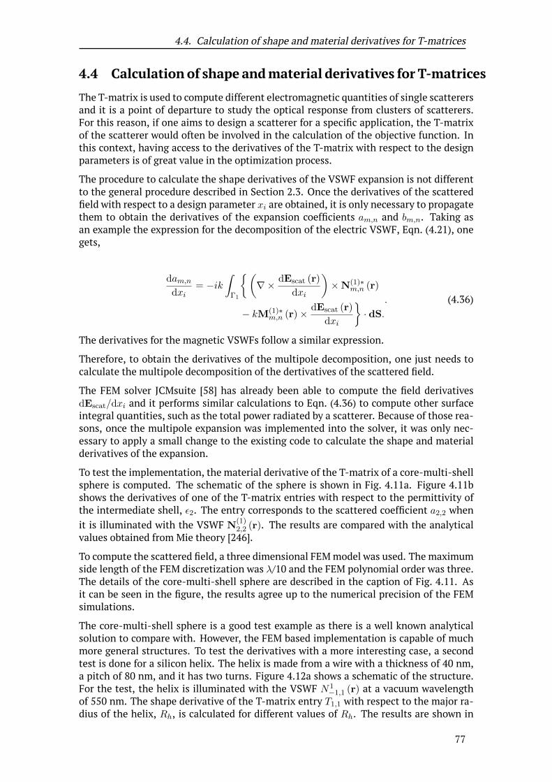
4.4. Calculation of shape and material derivatives for T-matrices
4.4 Calculation of shape andmaterial derivatives for T-matrices
The T-matrix is used to compute different electromagnetic quantities of single scatterersand it is a point of departure to study the optical response from clusters of scatterers.For this reason, if one aims to design a scatterer for a specific application, the T-matrixof the scatterer would often be involved in the calculation of the objective function. Inthis context, having access to the derivatives of the T-matrix with respect to the designparameters is of great value in the optimization process.
The procedure to calculate the shape derivatives of the VSWF expansion is not differentto the general procedure described in Section 2.3. Once the derivatives of the scatteredfield with respect to a design parameter xi are obtained, it is only necessary to propagatethem to obtain the derivatives of the expansion coefficients am,n and bm,n. Taking asan example the expression for the decomposition of the electric VSWF, Eqn. (4.21), onegets,
dam,ndxi
= −ik∫
Γ1
(∇× dEscat (r)
dxi
)×N(1)∗
m,n (r)
− kM(1)∗m,n (r)× dEscat (r)
dxi
· dS.
. (4.36)
The derivatives for the magnetic VSWFs follow a similar expression.
Therefore, to obtain the derivatives of the multipole decomposition, one just needs tocalculate the multipole decomposition of the dertivatives of the scattered field.
The FEM solver JCMsuite [58] has already been able to compute the field derivativesdEscat/dxi and it performs similar calculations to Eqn. (4.36) to compute other surfaceintegral quantities, such as the total power radiated by a scatterer. Because of those rea-sons, once the multipole expansion was implemented into the solver, it was only nec-essary to apply a small change to the existing code to calculate the shape and materialderivatives of the expansion.
To test the implementation, the material derivative of the T-matrix of a core-multi-shellsphere is computed. The schematic of the sphere is shown in Fig. 4.11a. Figure 4.11bshows the derivatives of one of the T-matrix entries with respect to the permittivity ofthe intermediate shell, ε2. The entry corresponds to the scattered coefficient a2,2 whenit is illuminated with the VSWF N
(1)2,2 (r). The results are compared with the analytical
values obtained from Mie theory [246].
To compute the scattered field, a three dimensional FEMmodel was used. The maximumside length of the FEM discretization was λ/10 and the FEM polynomial order was three.The details of the core-multi-shell sphere are described in the caption of Fig. 4.11. Asit can be seen in the figure, the results agree up to the numerical precision of the FEMsimulations.
The core-multi-shell sphere is a good test example as there is a well known analyticalsolution to compare with. However, the FEM based implementation is capable of muchmore general structures. To test the derivatives with a more interesting case, a secondtest is done for a silicon helix. The helix is made from a wire with a thickness of 40 nm,a pitch of 80 nm, and it has two turns. Figure 4.12a shows a schematic of the structure.For the test, the helix is illuminated with the VSWF N1
−1,1 (r) at a vacuum wavelengthof 550 nm. The shape derivative of the T-matrix entry T1,1 with respect to the major ra-dius of the helix, Rh, is calculated for different values of Rh. The results are shown in
77

Chapter 4. Design of isolated scatterers
R1R2
R3
a
1.5 2.0 2.5 3.0n2
−1.0
−0.8
−0.6
−0.4
−0.2
0.0
Re[ T
[8,8]]
b
T[8,8]
dT[8,8]
dn2analytic
dT[8,8]
dn2
−2
−1
0
1
2
3
Re
[ dT[8,8]
dn2
]
Figure 4.11: a. Schematic of the considered core-multi-shellsphere used to test the implementation of the material derivativesof the T-matrix. The core-multi-shell sphere is composed of threeconcentric spheres with radii 100 nm, 200 nm, and 300 nm respec-tively. Thepermittivities ε1 and ε2 are 12.25 and 6.25 respectively. b.Material derivative of one of the entries of the T-matrix with respectto the permittivity of the intermediate layer of a core-multi-shellsphere. The entry of the T matrix corresponds to the scattering co-efficient a2,2 when the sphere is illuminated with the fieldN
(1)2,2 (r).
Fig. 4.12. As there are no analytical results for the multipole decomposition of complexstructures such as helices available, the derivatives using the direct method were com-pared with the results obtained from finite difference calculations. As for the case of thecore-multi-shell sphere, the results of both methods agree up to a certain precision ofthe FEM simulation. Note that the results obtained using finite differences do not justrequire an extra simulation per parameter but they are also less accurate than the onesobtained using the direct method.
4.5 The adjoint method for multi-scattering problems
Description
One of the most relevant applications of the T-matrix is the calculation of the scatteredfield from clusters composed of many scatterers. Among other applications, the methodallows to rigorously solve the response of metalenses or the propagation of light throughaperiodic photonic crystals.
Finding the optimal shape or material properties of each of the scatterers to increase theperformance of the entire multi particle system, is generally a high dimensional opti-mization task. In this task, having access to the derivatives of the objective funtion withrespect to the shape or material parameters of the scatterers can drastically improve theconvergence of the optimization.
In the previous section, an implementation for computing shape andmaterial derivativesof T-matrices of complex scatterers was described and tested. This numerical method
78

4.5. The adjoint method for multi-scattering problems
Pitch
Twa
50 75 100 125 150
Rh (nm)
−0.09
−0.08
−0.07
−0.06
−0.05
−0.04
Re[ T
[1,1]]
b
T[1,1]
dT[1,1]
dRhf.d.
dT[1,1]
dRh
−0.0015
−0.0010
−0.0005
0.0000
0.0005
0.0010
Re
[ dT[1,1]
dR
h
]
Figure 4.12: a. Schematic of the helix used for computing theshape derivatives of the multipole decomposition. The helix ismade from a wire with a thickness, Tw, of 40 nm and a pitch of 80nm. Its refractive index is 3.5. b. Derivatives of one of the entries ofthe T-matrix with respect to the major radius of the helix, Rh. Theentry of the T-matrix links the scattering and illumination coeffi-cients a−1,1 and c−1,1 respectively. The illumination wavelength is550 nm.
can be used, in combination with a multi-scattering solver, to obtain the derivatives ofan objective function that depends on the field scattered by the entire system. The proce-dure to achieve this consists in combining the multi-scattering formalism with the director adjoint methods. Both methods were presented in section 2.3. In multi-scatteringproblems with clusters composed of a large number of particles, the adjoint method isfrequently used due to the large number of design parameters [255].
To describe the implementation of the adjoint method in multi-scattering problems, themulti-scattering formalism must be presented obviously at first.
Let us consider a system composed of a number of N scatterers, specified by their T-matrices T i. The multipole expansion of the field scattered by the scatterer i can berepresented by a vector Escat,i. As described in section 4.3, the T-matrix establishes arelation between the field that illuminates the scatterer i, Einc,i, and the correspondingscattered field,
Escat,i = T iEinc,i. (4.37)
In a system with many objects, the field scattered by each object partially illuminates allthe other objects. Therefore, the scattered field produced by each object is not only pro-duced by the external illumination as considered up to that point, but also as a responseto the fields scattered by the other scatterers. Denoting by Einc,i,0 the external illumina-tion on the scatterer i, one can write the total field illuminating a scatterer as
Einc,i = Einc,i,0 +∑
j 6=iEinc,i,j , (4.38)
79

Chapter 4. Design of isolated scatterers
whereEinc,i,j denotes the illumination field on the i-th particle due to the field scatteredfrom the j-th particle.
The link between the scattering and the illumination fields of the different scatterers canbe calculated using the translation theorems of the VSWF [42, 256, 257]. The translationcoefficients allow to construct the transformationmatrices between the scattered and theillumination fields,M i,j ,
Einc,i,j = M i,jEscat,j . (4.39)
OncematricesM i,j are obtained using the translation theorems, the equations describingthe whole system can be easily obtained. Denoting by Escat the vector expanding thescattered fields from all the particles
Escat =[ETscat,1,E
Tscat,2, ...,E
Tscat,N
]T, (4.40)
the system reads as
SMEscat = Escat,inc, (4.41)
where Escat,inc denotes the scattered field due to the external illumination, i.e., withoutconsidering the multiple interactions between the different scatterers,
Escat,inc =
T 1Einc,1,0
T 2Einc,2,0
T 3Einc,3,0...
TNEinc,N,0
, (4.42)
and SM is the system matrix
SM =
I −T 1M1,2 −T 1M1,3 . . . −T 1M1,N
−T 2M2,1 I −T 2M2,3 . . . −T 2M2,N...
...−TNMN,1 −TNMN,2 −TNMN,3 . . . I
. (4.43)
The solution of the above system gives the total scattered field. Once this system is ob-tained, the implementation of the adjoint system requires mainly onemore fundamentalstep: the calculation of the partial derivatives of the objective functionwith respect to thevalues of the solutionEscat. For this process, it is recommended to use software for auto-matic differentiation [258, 259], especially for complicated objective functions of Escat.After this step, one can solve the adjoint system,
SM †λ =dfob
dEscat. (4.44)
Note that here λ is used to denote the adjoint solution and not the wavelength. In thecontext it is used here, no confusion should appear.
Finally, the calculation of the derivatives of the objective function with respect to someparameter xi describing the geometry or material of one or more scatterers can be per-formed. This calculation is equivalent to the onedescribed inEqn. (2.103) for the FEM,
80

4.5. The adjoint method for multi-scattering problems
dfob
dxi= λT
(−dSM
dxi+
dEscat,inc
dxi
)(4.45)
The term dSMdxi
is obtained using the shape or material derivatives of the individual T-matrices for the single scatterers and applying the chain rule.
Example: metasurface hologram
cell[1,4]cell[1,3]cell[1,2]cell[1,1]
cell[2,1]
cell[3,1]
cell[4,1] cell[4,4]
R1[4,4]
R2[4,4]
Figure 4.13: Schematic of the hologram used to test the adjointmethod. The hologram is composed of a grid of 4 x 4 pixelsplaced along the plane z = 0. Each pixel is composed of a gridof 4 x 4 identical scatterers. The scatterers are disks with ahole in the center. The height of the disks is 300 nm for all thepixels. The disks are made from silicon and they are embeddedin a homogeneous medium with a refractive index of 1.44. Therefractive index of the disks is 3.6. The inner radii of the disks areR1 = [580, 242, 323, 8; 96, 71, 498, 14; 39, 30, 15, 70; 73, 96, 477, 183]nm, where the semicolon denotes the begin-ning of a new row. The outer radii are R2 =[601, 265, 426, 174; 175, 502, 533, 443; 397, 601, 412, 411; 80, 99, 497, 467]nm.
The adjoint method for the design of multi particle systems was implemented in Matlab.However, the implementation has not yet been integrated together with a package forperforming automatic differentiation. To test the implementation, the shape derivativesof the far-field produced by a small metasurface hologram are computed. The metasur-face is composed of a 4 x 4 pixel board. Each pixel is composed of a 4 x 4 periodic arrange-ment of identical scatterers. The scatterering elements of each pixel are silicon disks ofheight 300 nm that have a hole in the center, as shown in Fig. 4.13. The disks of each pixelare described by an inner and an outer radius. The refractive index of the silicon was con-sidered to be 3.6 for an illumination wavelength of 1550 nm. The embedding medium is
81

Chapter 4. Design of isolated scatterers
considered to have a refractive index of 1.44.
−0.08
−0.06
−0.04
−0.02
Re[E
y](V/m
)
EydEy
dRouter [3,2]f.d.
dEy
dRouter [3,2]
100 200 300 400 500
Router [3,2] (nm)
0.02
0.04
0.06
Im[E
y](V/m
)
−0.001
0.000
0.001
Re
[dE
y
dR
outer[3,2]
]
−0.0005
0.0000
0.0005
0.0010
Re
[dE
y
dR
outer[3,2]
]
Figure 4.14: Amplitude of the scattered field produced by the holo-gram described in Fig. 4.13 when it is illuminated by a plane wave.The derivatives of the scattered field are computed with respect tothe outer radius of the disks of the pixel [3,2]. The illuminatingplane wave has a wave vector oriented along the -z-direction. Itselectric field is linearly polarized in the x-direction. The vacuumwavelength of the plane wave is 1550 nm. The amplitude of thescattered field is measured at the point (0,0,-100λ0).
For this test example, the objective function consists of the value of the electric field in apointxprobe placed 100wavelengths away from themetasurface, at the point (0,0,-100λ0).The adjoint method was used to compute the derivative of the electric field with respectto the outer radius of the disks of the pixel [3,2]. The results obtained are shown inFig. 4.14 for different values of the radius. The shape derivatives computed with theadjoint method are compared with results obtained using finite differences. As shownin the figure, the results of both methods are in agreement. The T-matrices of the indi-vidual scatterers contain the multipole contributions up to the second, i.e. quadrupolar,order. This results in a system matrix SM with a size of 4096 x 4096.
The combination of a multi-scattering solver, the calculation of shape derivatives of in-dividual T-matrices and the adjoint method can be used to design complex multiparticlestructures. In the case of metasurface holograms, themethod could be used to rigorouslycalculate the field obtained in the image plane and to design the shape of the scattererswithin each pixel. With this method one could design a hologram that creates the de-sired image, taking into account all the interactions between the scatterers. Of specialinterest are the interactions between the scatterers of different pixels [260], which whennot taken into account, produce undesired effects. However, to solve practical systems,containing a large number of elements, it is necessary to implement an iterative solverfor the systems given by Eqns. (4.41) and (4.44) [220]. The reason for that is the quadraticscaling of the system matrix with the number of scatterers, that makes even the storage
82

4.6. Conclusions
of the system matrix in the computer memory impossible.
4.6 Conclusions
This chapter described different numerical implementations of relevance for the analysisand design of isolated scatterers. The main result, the expressions to decompose scat-tered fields into a VSWF basis using surfaces with general shapes, gave rise to a series oftools that have been implemented into a FEM solver. These tools include a method toobtain the multipole decomposition of complex geometries and the calculation of theirT-matrices. Of special interest in the context of the design of photonic devices is the im-plementation of shape and material derivatives for the T-matrices of complex scatterers.These shape derivatives are not only useful for the design of isolated scatterers, but theycan also be combinedwithmulti-scattering solvers andwith theuse of the adjointmethodto help in the design of systems composed of a large number of scatterers. Examples aremetasurface holograms,metalenses or aperiodic photonic crystals. Thismethodhas beendescribed and its implementation was tested. However, to obtain a more powerful tool,further improvements must be done, as the use of an iterative solver for linear systemsand the use of automatic differentiation to calculate complex objective functions.
83


5 | Application examples
The previous chapters introduced different numerical methods to optimize the design ofphotonic structures. This chapter is devoted to such design task. We present here thedesign of two optimal photonic structures: electromagnetic chiral scatterers and waveg-uide edge couplers. Both structures are of interest from different perspectives. Maximalelectromagnetic chiral scatterers present an extraordinary behavior with respect to theirinteractionwith circularly polarized planewaves of different handedness. In this context,wewant to study inmore detail what can be the frequency range that can support such ex-treme structures. The second type of structures studied, waveguide edge couplers, are animportant component for the interconnection of different photonic elements in photonicintegrated circuits. The design of efficient and compact edge couplers is required to theimplementation of photonic circuits that will enable the next generation of optical datanetworks.
The chapter is structured in two main sections, each of them corresponds to the designof each of the two mentioned photonic structures. In each section, we first introducethe structure, explain the main physical concepts related to it, and the relevance of itsoptimized design. After that, we present the optimization methodology used to designit, and we analyze the performance of the designs obtained.
5.1 Maximal electromagnetic chiral helices
Introduction
One of the applications for the previously established methods is the optimization ofelectromagnetically chiral objects. Here, the term chirality was first introduced in 1892by Lord Kelvin [261]. He suggested that an object is said to be chiral if it can not besuperimposed onto any mirror image of itself by applying any combination of rotationsand translations. If the object can be superimposed onto its mirror image, it is said to beachiral.
Chiral objects are present in many different fields of science. Many molecules are chiral,and they often exist as a pair of mirror images, called enantiomers. The enantiomershave exactly the same physical properties except in their interaction with other chiralobjects, such as other chiral molecules or, in the context of photonics, when interactingwith chiral states of light. In biology, most of the fundamental building blocks of life arechiral, including many carbohydrates and amino-acids [262]. As chiral molecules reactdifferently with other chiral objects, a pair of enantiomers can cause completely differentactions on living organisms. For example, the molecule that lens lemons and orangestheir odor is a specific enantiomer of limonene while the opposite enantiomer smells likepines [263]. Similarly, the interaction of a chiral molecule, or a chiral object in general,with light depends as well on the handedness of the illumination. This effect hasmultiple
85

Chapter 5. Application examples
applications, e.g., as a mechanism for chiral sensing of molecules [242, A7, A8, 253, 264–268], to trigger the production of different enantioselective reactions [269–271], or toimplement polarization filters [272].
If one aims to engineer an object that maximizes the difference in its interaction withlight of different handedness, one might think that designing a maximally chiral objectwould be a good design strategy. However, the first problem with this approach is thatchirality is a binary property, and it has been shown that no rigorous method to quantifychirality exists [273]. Different measures of chirality have been proposed, see for exam-ple [274]. However, all of them lead to some inconsistency. For example, it could be shownthat any tetrahedron can be defined as the most chiral one, even though it is only incre-mentally different from an achiral tetrahedron [275]. Based on the fact that a chiral ob-ject interacts differently with light of different handedness, ameasure of electromagneticchirality, χ, that mitigates some of these limitations has been recently proposed [213].Here, the emphasis should be put on electromagnetic chirality instead of chirality only, asit measures how different the object responses to electromagnetic radiation of differentchirality, or more precise helicity. The measure assigns a certain frequency dependentvalue, χ, to the object based on the interaction of the object with all possible illumina-tion fields of different helicity. This definition of the electromagnetic chirality, which wewill denote as em-chirality from now on, is compatible with the geometrical definitionof chirality. An achiral object will always present a vanishing χ value for all illuminationfrequencies. The link between the em-chirality and other electromagnetic quantities,such as circular dichroism [276] and one of the porposed measures for the geometricalchirality has been numerically studied in [A10].
One interesting property of the em-chirality is that it is upper bounded by the total in-teraction cross section of the particle. This characteristic allows for the definition of anormalized measure of the em-chirality, χ. If an object is maximally em-chiral, i.e. if itsχ is equal to 1, the object is invisible to any illumination that is a pure state of one of thetwo eigenstates of the helicity operator ([277] chapter 8). Such extreme objects could beused in very interesting applications. For example, in an angle independent polarizationfilter, as was proposed in [213], or for sensing schemes of chiral molecules.
The concept of maximally chiral objects with a χ value close to 1 has been studied in theliterature. A silver helix with a χ higher than 0.9 has been reported at a wavelength of200 µm [213]. Also, there are different design rules for obtaining such objects using idealperfect electric conductors of an extremely thin thickness [278]. However, it is not clearif similar results can be achieved at optical frequencies or in the near infrared.
This section presents the design of optimal silver helices with respect to their χ value.The aim of the work is to find out if it is possible to obtain objects that present high valuesof χ in different regions of the infrared and optical spectrum. To do that, the work com-bines different optimization and numerical methods presented within this thesis, suchas Bayesian optimization, the method to calculate the T-matrices of complex structures,and the calculation of the shape derivatives of the multipole decomposition.
The reason for using helices as the geometry to be optimized is based on existing re-sults that show that helices present strong differences in their interaction with planewaves of different handedness [272, 278–281, A11]. Also, the optimization of a helix isa simpler task than the optimization of more complex freeform wires, where one needsto impose complicated constraints to avoid self-intersections. Regarding the use of sil-ver as material, we chose it for a few reasons: One reason is that the simulations for thehigh em-chiral helix at the infrared reported in [213] used silver as material. Also, silverhas been reported to be a better material to sustain magnetic resonances at optical fre-
86

5.1. Maximal electromagnetic chiral helices
quencies [282]. This effect was also supported by some preliminary simulations that wemade at optical frequencies using gold helices, that showed lower em-chiral responsesthan similar silver helices.
In the following subsections, first the definition of χ is formally introduced. After that,the numerical procedure to perform the optimization is described. Finally, the last sub-section presents the optimization results and analyzes the optimal helices. The work andresults presented in this section correspondmainly to the results contained in [A12].
Electromagnetic chirality
The definition of the electromagnetic chirality [213] of an object, χ, is based on the mea-sure of the interaction of the scatterer with fields of different helicity. To obtain χ, oneneeds to first obtain the S-matrix characterizing the scatterer in a basis of VSWFs of purehelicity
G3,+−1,1...
G3,+nmax,nmax
G3,−−1,1...
G3,−nmax,nmax
= S±
G1,+−1,1...
G1,+nmax,nmax
G1,−−1,1...
G1,−nmax,nmax
=
[S++ S+−
S−+ S−−
]
G1,+−1,1...
G1,+nmax,nmax
G1,−−1,1...
G1,−nmax,nmax
. (5.1)
The S-matrix of an object can be obtained from its T-matrix by S± = I + 2T±. TheT-matrix was introduced in section 4.3 and both the scattering,G3,±
m,n, and illumination,G1,±m,n, vector sphericalwave functions of pure helicitywere introduced in section 2.2.
Once the S-matrix is obtained, one has to calculate two vectors, v+ and v−, obtainedfrom the singular values of the block elements of the S-matrix, S±,±
v+ =
[svd
(S+,+
)
svd(S−,+
)]v− =
[svd
(S−,−
)
svd(S+,−)
]. (5.2)
The summation of the squared entries of the two vectors gives the total interaction crosssection of the scatterer [213]
σint =∑
i
v+[i]
2+ v−[i]
2, (5.3)
which is linked to the rotationally averaged total scattering cross section of the object ([42]Eqn. 5.140).
The definition of χ is given by the distance between the vectors v+ and v−,
χ =
√∑
i
(v+
[i] − v−[i]
)2. (5.4)
The em-chirality χ is bounded between 0 and√σint, therefore one can define the normal-
ized em-chirality χ by dividing χ with√σint,
χ =χ√σint
. (5.5)
87

Chapter 5. Application examples
In [213] it was shown that an achiral object will always have a χ value of zero. One can seefrom the definition that if a scatterer has a χ equal to 1, the scatterer will only interactwith light of one of the pure states of the helicity operator. It implies that the scattererwill be transparent to light of one of the two helicity eigenstates. Also, for an object tobe maximally electromagnetic chiral it has to be dual. Note that the implication is notunidirectional: an achiral object can be dual, as it is the case for the cylinder optimizedin section 4.3.
Simulation setup
In this section we will describe the methodology that we use to design em-chiral silverhelices. Our intention is to find different optimal helices, each one of them presentinghigh em-chirality values at a different region of the optical and infrared frequency spec-trum.
To find these helices, we use the Bayesian optimization algorithm presented in chapter 3.We provide to the algorithm observations of χ and also of its shape derivatives with re-spect to the parameters that model the helices. To compute these quantities, we use thefinite element method solver JCMsuite [58, 229]. The calculation of the T-matrix usingthe FEM has been described in section 4.3. Section 4.4 has been describing how to obtainthe shape derivatives of the T-matrix.
For the case of the helix, the procedure that we use to obtain the shape derivatives ofthe actual mesh describing the helix with respect to the parameters of the helix involvesa series of steps, as shown in Fig. 5.1. First, the helix is discretized using the internalmesher of JCMsuite. Once the mesh of the helix has been obtained, we need to calcu-late the derivatives of the vertices of the boundary mesh elements with respect to theparameters that describe the boundary of the helix. Given a helix specified by the radiusof the spine, Rh, its thickness, Tw, the pitch, Pitch, and the number of turns, Nturns, theboundary of the helix can be parametrized with only two parameters θh and φh as
xhelix (θh, φh) = xspine (θh) +Tw
2(v1(θh) cosφh + v2(θh) sinφh) , (5.6)
where xspine are the points of the central spine of the helix
xspine (θh) =
(Rh cos θh, Rh sin θh,
P itch
2πθh
)(5.7)
and v1(θh) and v2(θh) are two unitary vectors that are perpendicular to the tangent of thespine of the helix, v3(θh). All these vectors are given by
v1(θh) = − (cos θh, sin θh, 0) , (5.8)
v2(θh) =
− Sh√
R2h + S2
h
sin θh,−Sh√
R2h + S2
h
cos θh,−Rh√
R2h + S2
h
, (5.9)
v3(θh) =
− Rh√
R2h + S2
h
sin θh,−Rh√
R2h + S2
h
cos θh,Sh√
R2h + S2
h
. (5.10)
In the above equation, the slope Sh is equal to Pitch/2π. The parameter θh ranges from 0to Nturns · 2π and φh ranges from 0 to 2π. Note the difference between the parameters of
88

5.1. Maximal electromagnetic chiral helices
2.1. 3.
Figure 5.1: Steps needed to compute the shape derivatives of theFEM discretization of a helix. The helix is determined by its de-sign parameters: the radius of the helix spine, Rh, the thickness ofthe helix wire, Tw, the Pitch of the helix, Pitch, and the number ofturns of the helix, Nturns. Given the parameters, the helix can bediscretized using tetahedra. After obtaining the discretization (1),a Python module is used to determine the parameters θh, and φh,Eqn. (5.6), for each vertex of the helix boundary (2). These param-eters are used to evaluate the expressions for the shape deriativesin the vertex (3). The shape derivatives of the vertices are finallypassed to JCMsuite.
the helix parametrization, θh and φh that specify the different points of the boundary ofthe helix and the parameters of the actual optimization, Rh, Tw, Pitch and Nturns, usedto specify the different helices within the design space.
To model helices with smooth surfaces, we place two hemispheres on the edges of thehelix. The parametrization used for the upper hemisphere is
xhelix (t, φh) =xspine (Nturns · 2π) + sin tTw
2v3 (Nturns · 2π)
+ cos tTw
2(v1(Nturns · 2π) cosφh + v2(Nturns · 2π) sinφh) , (5.11)
where t ranges from 0 to 2π. An ananlogous expression is used to parametrize the lowerhemisphere.
Given a vertex of the FEM discretization of the helix boundary, to calculate the parameterθh or t that corresponds to this vertex, we use a local optimizer that searches for thevalues that minimize the distance between the vertex and the spine of the helix givenby Eqn. (5.7). The initial parameter used in this local optimization is an approximationof the final retrieved value based on the z-component of the vertex. Once the value ofθh or t has been obtained, retrieving the value of φh is rather simple. One only needs tocalculate the angle between the vector xhelix − xspine and the vector v2.
89

Chapter 5. Application examples
Once the parameters corresponding to the vertex are retrieved, the final step is to com-pute the derivatives of the vertex with respect to the design parameters. For that, oneonly needs to evaluate the expressions for dxhelix
dRh, dxhelix
dTw, dxhelix
dPitch , anddxhelixdNturns
. These ex-pressions are analytically derived from Eqns. (5.6)-(5.11).
The described procedure is implemented into a Python module that is then passed toJCMsuite. JCMsuite evaluates the Python module for every vertex of the helix boundaryto obtain the shape derivatives of the vertices1. Then, based on these values, it computesthe derivatives of the FEM system matrix as described in section 2.3 to obtain the shapederivatives of the T-matrix, as explained in section 4.4. Figure 4.12 in the previous chap-ter shows the results for the test of the shape derivatives of the T-matrix of a helix.
To finally obtain the shape derivatives of the em-chirality, χ, one needs to propagate theshape derivatives of the S-matrix along equation (5.4). The part of this operation thatrequires the most attention is the calculation of the shape derivatives of the singularvalues, needed to obtain the vectors v+ and v−, Eqn. (5.2).
Let us denote by U , Σ, V the matrices that contain the singular value decomposition of,for example, S+,+,
S+,+ = U †ΣV , (5.12)
U †U = I, (5.13)
V †V = I, (5.14)
where † denotes the transpose conjugate.Now, let us assume that we know the shape derivative ofS+,+ with respect to some designparameter xi. Then, one can obtain the shape derivative of the singular values of S+,+
as [283]
dΣ
dxi= I
(Re
[U †
dS+,+
dxiV
]), (5.15)
where denotes the element-wise multiplication and I is the identity matrix.The calculation of the shape derivatives of the singular values is simple once the shapederivatives of the S-matrix have been obtained, if the singular values are not degenerate.However, things becomemore complicated for the casewhere one ormore singular valuesare degenerate. The singular value decomposition is discontinuous within the subset ofmatrices with degenerate singular values [284]. A similar behavior occurs for the eigen-value decomposition [285]. One simple example of a parametric object for which this canhappen is a spheroid, where the value of the major axis is given as a design parameter.If one considers the simpler case of an S-matrix with only the dipole contributions, thesubmatrices S±,± will have a singular value with a triple degeneracy when the spheroidbecomes a sphere. A change in the value of themajor axis with respect to this point wouldlead to submatrices that have a singular value with a double degeneracy, therefore stillbeing degenerate. If instead the infinitesimal change in the parameter leads to a ma-trix without degenerate singular values, the differentiability of the singular values withrespect to the parameter depends on the properties of the parametric matrix [284]. Tomake the process simpler, we do not consider the derivatives of χ when we detect that
1The team from JCMwave GmbH created the bridge into JCMsuite for us to be able to pass the shapederivatives of complicated structures to the software using our own Python modules.
90

5.1. Maximal electromagnetic chiral helices
any of the singular values are degenerate. As we use Bayesian optimization, the correctfunctioning of the algorithm does not depend on providing derivative observations ornot. The shape derivatives are extra information that the Gaussian processes can use toobtain a better model of the objective function. However, the Gaussian process can in-corporate derivative observations for just some of the evaluated points, or even includederivative observations with respect to some parameters and not to the others.
Once the derivatives of the vectors v+ and v− are obtained, the shape derivatives of χread as
dχ
dxi=
∑i
(v+
[i] − v−[i]
)(dv+
[i]
dxi− dv−
[i]
dxi
)
χ. (5.16)
A similar expression can be obtained for the derivatives of the total interaction crosssection,
dσint
dxi=∑
i
2v+[i]
dv+[i]
dxi+ 2v−[i]
dv−[i]dxi
. (5.17)
Finally, one can obtain the derivatives of χ as
dχ
dxi=
dχdxi
√σint − χ
2√σint
dσintdxi
σint, (5.18)
As we can see in Eqn. (5.16), the derivative of χ is also not defined when χ equals zero.As for the case in which the discontinuity of the derivatives comes from the singularvalue decomposition, we simply check if χ is zero and in this case we do not include thederivatives of χ into the optimization process.
Results of the optimization
After having described the simulation and optimization setups, we proceed to optimizethe em-chiraliry of silver helices at a decreasing set of design wavelengths. It is our in-tention to study how the geometry of an optimal helix changes when operating at lowerwavelengths and which upper value for the em-chirality can be obtained when workingat optical wavelengths and not in the far-infrared. We would like to see a lower bound fora wavelength where a high em-chirality is obtained. Based on the material properties ofsilver, it can be expected that this happens somewhere at the wavelengths correspondingto visible light.
The optimizations depart from a desig wavelength of λ0 = 150 µm down to a wavelengthof λ0 = 500 nm. The reason for starting at such a long wavelength value is based onexisting results for a silver helix [213] that presents a large χ in this frequency region.These results give us an estimation about the bounds to use for the design parameterspace.
At the wavelength of λ0 = 150 µm the lower and upper limits of the radius of the helix,Rh,are set to 1 µmand 10 µmrespectively. Both limits are linearly scaledwith thewavelengthfor the optimizations performed at the other different wavelengths. The thickness of thewire can vary between a 5% and a 95% of the value of 2Rh. A further bound is imposed onthe thickness of the wire, it can not be thinner than 20 nm for any of the optimizations.
91

Chapter 5. Application examples
This extra limit is included to restrict the results to helices that are in the limits of what itis possible to realize experimentally using current fabrication technologies. Moreover, awire with a thickness of 20 nm is close to the limit for which the electromagnetic responseof the object can be described using the macroscopic constitutive relations (see, e.g., [41]section 6.6). The pitch of the helix is bounded between 1.1 and 10 times the thicknessof the wire and the optimization limits for the number of turns are 0.1 and 4. The per-mittivity of silver is interpolated at each wavelength from two different databases [286,287] depending on the frequency region. One database accounts for the optical and near-infrared regions and the other for wavelengths longer than 1.5 µm.
Regarding the calculation of χ, we use finite elements with a polynomial degree of 2. Themaximum side length of the helix mesh elements is λ/0.3 for illumination wavelengthslonger than 2 µmand λ/10 for the optical and near-infraredwavelengths, i.e. shorter than2 µm. Here, λ refers to the wavelength within the helix. The maximum side length of theelements in the air domain is set to λ0/15. Before starting each optimization, a conver-gence test with respect to themesh size is done to check the accuracy of the results. Whenthe error with the default mesh size is larger than 1%, the mesh size is further decreased.In many situations it is favorable to use a higher polynomial degree when compared tousing smaller mesh elements. However, in this specific application it is important forthe accuracy of the results to have an accurate representation of the surface of the helix.Therefore, it is preferable to have smallermesh elements rather than a higher polynomialdegree.
100 101 102
λ0 (µm)
0.6
0.7
0.8
0.9
1.0
χ
Figure 5.2: Values of the normalized em-chirality, χ, of the optimalhelices obtained in the optimization runs as a function of the designwavelength. Each point corresponds to the value of a different helixoptimized for the corresponding wavelength shown in the x-axis.The design parameters of the optimal helices are shown in Fig. 5.3.
Figure 5.2 shows the optimal values of χ obtained at each optimization wavelength. Thecorresponding parameters of the optimal helices are shown in Fig. 5.3. As it can be seenin Fig. 5.2, the optimal χ values are all above 0.9 for wavelengths down to 3 µm. However,the optimal χ values already start to decrease with the wavelength from a wavelength ofλ0 = 10 µm. Below λ0 = 1 µm, the decrease is very abrupt and at λ0 = 500 nm χ does notreach a value of 0.6.
The two different behaviours for the wavelength regions above and below λ0 = 3 µm be-
92

5.1. Maximal electromagnetic chiral helices
comes clear after simultaneously inspecting both Fig. 5.2 and 5.3. Except for the optimalhelix found at λ0 = 150 µm, all the designs that show a χ above 0.9 have a similar shape.The number of turns keeps more or less constant along this region and it seems to ex-ist a common ratio between the radius of the helix spine Rh and the pitch of the helix.Moreover, the absolute values for both parameters seem to follow a linear scale with thewavelength. These relations seem to indicate that the different optimizations found anoptimal design that simply downscales with the wavelength. This behaviour can be ex-pected as at thesewavelengths the helices can bewell approximated as helicesmade froma perfect electric conductor. Scaling of the geometrical parameters then indeed scales theoperation wavelength. In fact, if one takes the optimal design found at λ0 = 100 µm andscales down the radius and pitch of the helix following the scaling rule for plasmonicmaterials described in [238] , as already done in section 4.2 for the nanorod, one obtainsthe dashed black line shown in Fig. 5.3. Only for the design wavelengths in the rangebetween 3 µm and 10 µm this scaling factor with respect to the wavelength slightly differfrom unity. The optimal designs clearly follow the scaling design rules for perfect elec-tric conductors under the thin wire approximation. There are still some small differencesthat can come from the fact that the FEM simulations take the effects produced by thethickness of the wire rigorously into account. Even if the thickness of the wire is muchsmaller than the illumination wavelength, it can play a significant role in the scatteringresponse of the helix [288].
100 101 102
λ0 (µm)
102
103
Optimalparametersofthehelix(nm) Rh Tw Pitch Nturns Rh,eff
1.5
2.0
2.5
3.0
OptimalN
turn
s
Figure 5.3: Design parameters of the optimal helices obtained inthe optimization runs made for different design wavelengths. Thedesign parameters are the radius of the helix spin,Rh, the thicknessof the helix wire, Tw, the pitch of the helix, Pitch, and the numberof turns of the helix, Nturns. The schematic of Fig. 5.1 shows themeaning of the different parameters in more detail.
Regarding the results for the shorterwavelengths, one of the reasons explaining the lowerχ values at wavelengths below 1.5 µm compared to the values obtained at longer wave-lengths could be the lower bound of 20 nm imposed for the thickness of the wire. As it canbe seen in Fig. 5.3, the thickness of the wire of the helix is lower than 30 nm for all the op-timal helices found at wavelengths below 3 µm. This could indicate that for wavelengthsbelow 3 µm the ability to achieve optimal em-chiral values is constrained by the helixthickness. However, the reason behind the drop of the optimal χ values is more likelyto be due the plasmonic behaviour of silver at these frequencies. Due to the increaseof Ohmic losses and the internal reactance of the silver wire, it becomes more difficultto obtain strong magnetic resonances when one approaches the plasma frequency, as it
93

Chapter 5. Application examples
was reported in [282, 289, 290]. Obtaining electric and magnetic resonances of a similarstrength is crucial to obtain a strong chiral response [247, 291].
To analyze the interactions of a high em-chiral helix with light of different helicities, weconsider from now on the helix optimized for a design wavelength of λ0 = 3 µm. Fig-ure 5.4 shows the spectral dependent total interaction cross section, σint, and the nor-malized em-chirality, χ, for wavelengths around the optimization wavelength. The totalinteraction cross section is obtained as the squared Frobenius norm of the scattering sub-matrices S+,+ and S−,− respectively as
σint,+ =∑
i,j
|S+,+[i,j] |
2, (5.19)
σint,− =∑
i,j
|S−,−[i,j] |2. (5.20)
As one can see in Fig. 5.4, the maximum in the chirality also corresponds to a resonancepeak in the total interaction cross section. It implies that the chirality is not just largeat some trivial point where not much light is scattered. Figure 5.5 shows the absorptioncross section of the helix when it is illuminated with two circularly polarized plane wavesof opposite handedness. The absorption cross sections are shown as a function of thedirection of the wave vector of the plane wave used for the illumination. Similar to theresults shown in Fig. 5.4 for the total interaction cross section, the absorption is almosttwo orders of magnitude higher for right circularly polarized plane waves. The strongestdifference occurs for plane waves whose wave vectors are parallel to the xy-plane, i.e.,perpendicular to the helix axis.
2.0 2.5 3.0 3.5 4.0
λ0 (µm)
10−4
10−3
10−2
σint
σint,+ σint,− χ
0.2
0.4
0.6
0.8
χ
Figure 5.4: Wavelength dependency of the total interaction crosssections, σint,±, and normalized em-chirality, χ, of the optimal he-lix obtained from the optimization at the design wavelength of λ0
= 3 µm. The total interaction cross section is given as a functionof the helicity eigenstate of the illumination. The plus and minussigns in the subscript of σint indicate the eigenvalues ±1 of the twoeigenstates of the helicity operator.
94

5.1. Maximal electromagnetic chiral helices
−1 0 1
kx/k0
−1.0
−0.5
0.0
0.5
1.0ky/k
0
−1 0 1
kx/k0
−1.0
−0.5
0.0
0.5
1.0
ky/k
0
10−2
10−1
100
σ− abs
( µm
2)
10−2
10−1
100
σ+ abs
( µm
2)
Figure 5.5: Absorption cross section, σabs, of the optimal helix ob-tained from the optimization at λ0 = 3 µm depending on the di-rection of the illuminating plane wave. The helix is illuminatedwith a circularly polarized plane wave at a wavelength of λ0 = 3µm. The two different plots correspond to the results for the twodifferent circular polarization states, denoted with the plus sign,σabs,+, for right circular polarized plane waves and with the minussign, σabs,−, for left circular polarized plane waves. The directionof the wave vector of the plane wave is given as a function of thex and y-components of its unitary vector. k = (kx, ky, kz) with|k|2 = k2
x + k2y + k2
z = k20.
Figure 5.6 shows the intensity of the scattered near-field produced by the helix when illu-minated by two circularly polarized planewaves of different handedness andwave vectorsparallel to the x-axis. The optimized helix also shows strong differences of around twoorders of magnitude in the scattered field intensity. As one can see, for the right circu-larly polarized plane wave, the scattered field intensity is strongly localized inside thehelix. This intense near field is linked to the high absorption of light in the helix.
All these results indicate that the designed helix could serve as the basic constitutive el-ement for an angle independent circular polarization filter. The filter would consist of aslab made from a homogeneous material with a high number of randomly oriented andrandomly placed helices embedded into it. To analyze the potential of the design, wewill estimate the slab thickness required to absorb 99% of the incoming power flux ofa circular polarized beam and compare it to the power absorbed by a beam with oppo-site handedness. As we optimized the helices assuming that they are embedded into freespace, we will assume now for simplicity that the embedded material has a relative per-mittivity of 1. For this calculation, we will make a series of additional approximations.Mainly, we will neglect scattering and consider that absorption is the only mechanism ofinteraction of the helices with the incident light. We will also assume that the incomingbeam can be approximated by a plane wave. That is, let us assume that the incomingbeam has an isotropic power flux with direction +z. Lastly, we treat the combination ofthe slab plus helices as a single homogeneous material, neglecting the discrete nature ofthe helices. The volume of the optimal helix obtained at λ0 = 3 µm is 0.00106 µm3. If wenow assume a volume filling fraction of 1%, that implies a density of ρh = 9.65 helices percubic µm.
Let us now focus on a volume element of the slab with a square section of side lengthl equals to 1 µm and thickness t, as shown in the sketch of Fig. 5.7. We want to studyhow the power flux of the incident beam changes along the z-direction within the slab.
95

Chapter 5. Application examples
0
50
100
150
200
250
300
|Escat|2(V m
) 2
x
zk k
Figure 5.6: Intensity of the field scattered by a helix as a function ofthe handedness of the illuminating circularly polarized plane wave.The results are shown for the optimal helix obtained from the opti-mization run at λ0 = 3µm. The illumination direction relative to thehelix is indicated in the top of the figure.
The absorption cross sections under plane wave illumination of the rotationally averagedoptimal helix are for the right and left circularly polarized plane wave σabs,+ = 0.36 µm2
andσabs,− = 0.0075µm2 respectively. We computed these values as the difference betweenthe orientation averaged extinction and scattering cross sections.
The power absorbed by each of the helices equals the product of the illumination powerflux times the absorption cross section of the helix
Pabs(z) = Sz(z)σabs,±. (5.21)
In a volume of thickness∆z and area l2 the power absorbed per unit area equals
Pabs(z + ∆z)− Pabs(z)
l2= ∆z ρh Sz(z)σabs,±, (5.22)
where∆z is considered to be thin enough to assume that the power flux remains constantthroughout the thickness. Note that the homogenization of thematerial properties of theslab with the embedded helices is also included through the use of ρh.
Therefore, the change in the power flux of the beam per unit of thickness equals,
Sz(z + ∆z)− Sz(z)∆z
= −ρh Sz(z)σabs,±. (5.23)
The differential equation for the power flux of the beamalong the slab can then bewrittenas
dSz(z)
dz= −Sz(z) ρh σabs,±. (5.24)
Solving the above differential equation one obtains
96

5.1. Maximal electromagnetic chiral helices
Figure 5.7: Sketch of the proposed angular independent polariza-tion filter. The filter consists of a slab with randomly oriented andrandomly placed optimally designed helices. Because the averagedabsorption cross section of the helices is different for illuminationfields of different helicities, the decay of the field along the slab willbe more pronounced for one of the illumination fields.
Sz(z) = Sz,0e−ρhσabs,±z, (5.25)
being Sz,0 the power flux of the incident beam before entering the slab.
Using the values obtained for the absorption cross sections and assuming a filling fractionof 1%, Eqn. (5.25) gives a slab thickness of 1332 nm to absorb 99% of the incident powerflux of a right circularly polarized beam. The same slab absorbs only 9% of the incidentpower flux for the beam with opposite handedness. These results show an extremelycompact device that presents a high performance, indicating the potential for photonicapplications of structures with high em-chirality values.
Conclusions
In the just presented application, we combined most of the tools developed within thethesis to find helices that offer high em-chirality values at optical and near infrared fre-quencies. The combination of Bayesian optimization, the tools to compute the T-matrixof isolated scatterers, and the calculation of its shape derivatives allowed us to find op-timal helices along a wide range of frequencies going from the deep infrared down tooptical frequencies. The results show that it is possible to design scatterers that presentlarge values of χ at frequencies down to 3 µm, but also the difficulties that exist in ob-taining similar results at optical frequencies. However, although we could not find silverhelices that present extremely large χ values at optical frequencies, it is still not clear ifother designs different than a helix could improve the results obtained here.
Once the optimizations were finished, we analyzed the behaviour of the optimal helixobtained for an illumination wavelength of 3 µm. The designed helix shows a strong dif-ference in the interaction with circularly polarized plane waves of different handedness.The interaction is close to two orders of magnitude stronger for one of the handedness,both in scattering and absorption.
To investigate the potential of these highly em-chiral objects, we calculated, based ona series of assumptions, the performance of a possible implementation of an angle in-
97

Chapter 5. Application examples
dependent circular polarization filter. The results indicate that it is possible to achieveextremely compact devices that at the same time present a high performance. Althougha more rigorous analysis is needed to confirm these results and possibly also to reducethe amount of simplifications used, they already give an idea of the potential that suchhigh em-chiral scatterers may have for different applications.
Further developments along the lines of this work can be the optimization of more com-plex structures, such as wires following a freeform path, to improve the em-chirality val-ues obtained at optical frequencies, or the optimization of designs that are inherentlyeasier to fabricate.
98

5.2. Waveguide coupler for photonic inter-chip communication
5.2 Waveguide coupler for photonic inter-chip communica-tion
Introduction
Photonic integrated circuits [292–294] emerge as a technological solution to the increas-ing demand for higher bit rates and lower energy consumption in communication net-works [295] and supercomputer clusters [296]. Due to the high data transfer rates thatcan only be achieved using light as an information carrier, the use of photonic circuitshas been also proposed in computing chips [297–302]. First proposals date back to the1980s [303–305]. Awell known problem that this technology could solve is the processor-memory bottleneck [306, 307].
A photonic integrated circuit contains a series of different interconnected optical com-ponents, such as lasers [308–310], modulators [311–315], optical switches [316–320],waveguides [321–326] or detectors. These circuits are generally used in the interfacesof the communication ports between the different nodes of an optical communicationnetwork.
One of the key techonological advances that made it possible to increase the perfor-mance of photonic integration circuits is the fabrication of photonic components us-ing the CMOS fabrication process, a technology known as silicon photonics [327–330].This results in high volume production, high densities, low costs and a better integra-tion with CMOS electronic circuits. The monolithic integration of the different photoniccomponents with CMOS electronic circuits would be a major step in the performanceand capabilities of the technology. However, photonic integrated circuits with betterperformances can currently only be obtained by combining in a single package photoniccomponents fabricated on different material platforms [331, 332]. One of the main chal-lenges to obtainmonolithic integration is the fabrication of laser sources on silicon [333–335]. Therefore, frequently light sources are made from III-V semiconductors while allthe other passive elements used to steer the light are made from silicon materials. Then,the components from these different material platforms need to be combined.
In a hybrid architecture that combines the beneficial aspects of different material plat-tforms, one promising technique to interconnect the different photonic platforms withinthe chip package is via three dimensional freeform waveguides, also called photonic wirebonds (PWB) [336–340]. Photonic wire bonds are polymer waveguides with three di-mensional freeform geometries. They are fabricated by two-photon polymerization of anegative-tone resist using a technology such as direct laser writing. Photonic wire bondscan be fabricated in situ and their geometry can be precissely controlled. This allowsfor the adaptation of their position to the position of the integrated waveguide facets,avoiding the high-precision alignment problems between optical components.
The basic architecture of this optical communication scheme is depicted in Fig. 5.8. Thewaveguide facets of two different chips are interconnected using a PWB. At each edgeof the PWB, a waveguide edge coupler is placed to efficiently couple the light betweenthe PWB and the waveguide. Aditionally, grating couplers may be needed if out-of-planecoupling between the waveguide connected to the PWB and some of the chips is required.All these components play a fundamental role in the overall efficiency of the system andthey need to be properly designed to reduce energy losses. The PWB path needs to beoptimized to reduce energy losses [341] as well as the shape and dimensions of the edgecouplers. It is also desirable that all the components have a footprint as small as possible.In this work, we focus on the optimized design of the edge coupler.
99

Chapter 5. Application examples
Si
Si
PWB
0.22
1.8
2
zx
Si
PWB
0.5
2
yxcladding cladding
Si photonic chip
Edge coupler Edge coupler
Grating coupler Grating coupler
PWB
Input
SMFOutput
SMF
Coupler
Coupler
zx
Figure 5.8: Schematic of the architecture for an optical inter-chipcommunication system.
As shown in Fig. 5.8, in the region of the edge coupler both the silicon waveguide and thePWB are placed on top of a layered substrate, therefore, the bottom part of both waveg-uides are vertically aligned. The cross sections of both waveguides are shown in Fig. 5.9.The silicon waveguide has a width of 0.5 µm and a height of 0.22 µm. The width andheight of the PWB are 2 µm and 1.8 µm respectively. The substrate is composed of twolayersmade of silicon (Si) and silica (SiO2). The silica layer has a thickness of 2 µmandweconsider the silicon layer to be semi-infinite. Thewaveguides are immersed in a cladding,characterized by its relative permittivity, εcladding.
An edge coupler is a passive photonic component used to efficiently connect opticalwaveguides that have different geometrical cross-sections and that are made from dif-ferent materials. We aim to design a structure that efficiently couples the fundamentalmode of the silicon waveguide into the fundamental mode of the PWB. See section 2.2 forthe description of the propagating modes in a waveguide. Figure 5.10 shows the electricfield intensity cross section of the fundamental modes of both the silicon waveguide andthe PWB. The modes are computed with JCMsuite [58], using two-dimensional layoutsconsisting of the cross sections of the waveguides. The fundamental mode of the sili-con waveguide has an effective refractive index of neff,PWB = 2.458 and its electric field ispredominantly polarized in the y-direction. The fundamental mode of the photonic wirebond is also predominantly polarized in the y-direction and it has an effective refractiveindex of neff,PWB = 1.473. If there were not substrate and the cross section of the PWBwere a perfect square, then the PWB would have a fundamental mode degenerated intotwo modes: one y-polarized and another z-polarized. However, the broken symmetry ofthe structure with respect to the z-direction avoids this degeneracy and produces twomodes with different propagation constants. The effective refractive index of the pre-dominantly z-polarized mode has a value 0.0003 lower than the one of the fundamentalmode.
100

5.2. Waveguide coupler for photonic inter-chip communication
SiO2
0.22 μm
zy
2 μm
0.5 μm
Si
SiO2
1.8 μmz
y
PWB
2 μm
2 μm
Si
Figure 5.9: Cross sections of the silicon waveguide, left, and thephotonic wire bond waveguide, right. Both elements are placed ontop of a layered substrate composed of silica (SiO2) ad silicon (Si)and are embedded into a material with a permittivity of εcladding atthe operating wavelength of 1.55 µm.
The coupling loses between the two guiding components are due to the mistmatch in thefield profiles of the fundamental modes. The basic working principle of the edge cou-pler consists in modifying the field profile along the propagation through the couplerto achieve a better overlap at its edge. Because edge couplers are an important compo-nent for the in-plane interconnection between optical fibers andwaveguides, their designand performance have been widely studied andmultiple reasonable structures have beenproposed. The most frequent solution is to use adiabatic linear tapers [342–346]. Anadiabatic taper is a waveguide whose lateral dimensions decrease gradually along the di-rection of propagation of light. Along the taper, the fundamental mode of the waveguidecan no longer be confined in the core of the waveguide due to the reduction of the dimen-sions and the field profile of the mode gradually expands towards the clading. To reducelosses due to mode conversion into higher modes, the profile of the taper has to changeslowly. As a result, adiabatic tapers present high coupling efficiencies but they also re-quire large footprints. In addition to linear tapers, other profiles have been proposedfor adiabatic tapers, such as tapers with parabolic [347] or exponential [348] profiles ormulti-section tapers [344, 349]. Other types of flat designs, such as meta-material basedcouplers [350–353], trident tapers [354–357], or combinations of both types [358] havebeen also designed.
To improve the mode matching in the vertical direction as well, different structures havebeen proposed. The adiabatic linear taper with a linear vertical profile is a natural ex-tension of the linear taper [359, 360]. Another strategy to improve the vertical overlap,which involves a less complex fabrication process, consists in encapsulating the waveg-uide inside an additionalmaterial layer, generally a polymer, which has a permivitty valueclose to the one of the waveguide with the lower refractive index [361, 362]. Other designstrategies can be found in dedicated review articles [363, 364].
In the following sections, we optimize and analyze the performance of two different de-sign proposals for the silicon waveguide-PWB edge coupler. The first design is a linearplanar adiabatic taper covered with an additional layer made of the same polymer as thePWB. A difference with the previously mentioned structures [361, 362], is that in thiscase the vertical profile of the covering layer also varies along the propagation directionof light. An interesting aspect is to not only see the maximum efficiency achievable withthis type of edge coupler but also to see how this efficiency depends on the length of thetaper and what is the minimum footprint achievable without considerable penalizing thecoupling efficiency. The second design proposed is based on a taper with a flat vertical
101

Chapter 5. Application examples
0.0
0.5
1.0
1.5
2.0
2.5
3.0
3.5
|E|2(V m
) 2
×1015
0.25
0.50
0.75
1.00
1.25
1.50
1.75
2.00
|E|2(V m
) 2
×1014
Figure 5.10: Electric field intensity of the fundamental modes ofthe silicon waveguide, left, and the photonic wire bond, right. Thegeometrical cross sections of the waveguides are shown in Fig. 5.9.The simulations were done with JCMsuite [58], using a finite ele-ment polynomial degree of 3 and a mesh side length of λ/5. λ isthe wavelength of the electromagnetic field in each material. Thevacuum wavelength is λ0 = 1.55 µm. Both intensity field profilesobtained are normalized to powers of 1 W.
profile and a freeform horizontal profile. We decided to investigate this structure basedon the results obtained for a two dimensional simplification of the same coupler [A2]. Fi-nally, we compare the performance of both design proposals and analyze the differencesin their working principles.
Parametric waveguide coupler
The schematic of the proposed adiabatic taper is shown in Fig. 5.11. The coupler is pa-rametrized with four parameters: its length, ltaper, the height, hPWB,taper, and width,wPWB,taper, of the photonic wire at its edge, and the width of the silicon waveguide atits edge, wSi,taper.
2 μm
zx
SiO2
Si
Si
0.22 μm
1.8 μm
Si waveguide
hPWB,taper
2 μm
yxSiO2
Si
0.55 μmwPWB,taper
ltaper
wSi,taper
Figure 5.11: Schematic of the parametric waveguide coupler. Thecoupler is parametrized by its length, ltaper, the height, hPWB,taper,andwidth,wPWB,taper, of the photonicwire bond at its opening facetand by the width of the silicon core of the taper at its edge, wSi,taper.
The coupler is optimized to find the design with the maximum coupling efficiency be-
102

5.2. Waveguide coupler for photonic inter-chip communication
tween the fundamental modes of both the silicon waveguide and the photonic wire bond.To calculate the coupling efficiency, ηcoupler, we use a three-dimensional finite elementmodel of the coupler. The coupler is illuminated with the incoming fundamental modeof the silicon waveguide and the total field, E(r), is computed. After the finite elementproblem is solved, we obtain the coupling efficiency through the calculation of the modeoverlap between the solutionE(r) and themagnetic field profile of the fundamentalmodeof the photonic wire bond,H0,PWB(r),
ηcoupler =
∣∣∣∣1
2
∫
S(E(r)×H0,PWB(r)) · xdS
∣∣∣∣2
, (5.26)
with S being a y-z-plane that cuts the photonic wire bond. This position of S correspondsto the right side in the sketches of Fig. 5.11. The above expression gives us directly thecoupling efficiency because the values used for the field intensity of the fundamentalmode of the PWB, shown in Fig. 5.10, are normalized to give a power carried by the guidedmode of 1 W.
Figure 5.12: FEM discretization of the waveguide coupler. Due tothe symmetry of the structure, only half of the device needs to bediscretized for the finite element method simulation.
As the coupler is symmetric with respect to the plane y = 0, we use a mirror boundarycondition to halve the size of the computational domain of the finite element method.Figure 5.12 shows an example of the finite element discretization of the parametric cou-pler for certain values of the design parameters. We use a finite elementmesh side lengthof λ/1.5, where λ is the wavelength of the illuminating inside the respective material.The finite element polynomial degree is set to three. The large size used for the meshelements is because of computational constraints. Our intention is to analyze couplerswith lengths up to 60 µm. That means couplers 100 times longer than the wavelengthwithin the core region of the silicon waveguide and the photonic wire bond. Even usingthis coarse discretization, the simulation of the longer couplers requires memory capac-ities exceeding 300 GB. Despite the coarse mesh used, a convergence test showed thatthe error produced in the coupling efficiency with this mesh is lower than three percent.The adiabatic character of these long tapers, which results in smooth field profiles in thetransition between the silicon waveguide and the photonic wire bond, is the main reasonfor this low error.
To obtain the optimal parameters of the coupler, we use the Bayesian optimization as
103

Chapter 5. Application examples
1 2
wPWB,taper (µm)
20
40
60
80
100
η coupler(%)
0.5 1.0 1.5
hPWB,taper (µm)
20
40
60
80
100
η coupler(%)
20 40 60
ltaper (µm)
20
40
60
80
100η c
oupler(%)
0.2 0.4
wSi,taper (µm)
20
40
60
80
100
η coupler(%)
Figure 5.13: Coupling efficiencies of the different designs evalu-ated during the optimization process of the linear taper edge cou-pler. Each figure show the projection of the coupling efficiency val-ues over the different parameters of the design space. The parame-ters are defined in the schematic of Fig. 5.11.
described in chapter 3. In this case, we do not use shape derivatives in the optimizationprocess. The design parameter space is composed of only four parameters and for thisproblem we expect the objective function to have a smooth behaviour with respect to thedesign parameters. Under these conditions, and based on the fact that creating an algo-rithm that provides the shape derivatives to JCMsuite would be a rather time consumingtask for this geometry, the benefit of using the shape derivatives is not clear.
We left the optimization to run for a couple of weeks. Let us note that each three di-mensional simulation of a candidate design needs a few hours to run on the availablecomputational infrastructure. The values of the coupling efficiency obtained during theoptimization process are shown in Fig. 5.13. The figure shows the projection of the evalu-ation points into each one of the parameters of the design space. The optimization limitsused for the design parameters can be seen in the axis of the different plots. The opti-mal design couples 99% of the input power into the fundamental mode of the photonicwire bond. For values of ltaper between 20 and 30 µm, the optimizer did not find designswith efficiencies higher than 90%. A strong correlation between the coupling efficiencyand wSi,taper is also visible. Contrastingly, there is no visible correlation of the couplingefficiency with the parameters wPWB,taper and hPWB,taper. This lack of correlation can beexplained by the fact that at the leftmost side of the taper the field is still strongly con-fined within the core of the silicon waveguide. Therefore, the field is insensitive to theeffect of the dimensions of the photonic wire bond cladding in this region. The optimal
104

5.2. Waveguide coupler for photonic inter-chip communication
0 10 20 30 40 50
x (µm)
−202
y(µm)
z = 0.11µm
0 10 20 30 40 50
x (µm)
0.0
2.5z(µm)
y = 0µm
10910121015
|E|2(V m
) 2
10910121015
|E|2(V m
) 2
Figure 5.14: Intensity field profile of the optimal linear edge cou-pler over the planes defined by the equations y = 0 µm and z = 0.11µm. The shape of the optimal coupler is represented in the figuresby the dashed lines. The blue dash line represents the boundaryprofile of the silicon core waveguide. The orange dash line repre-sents the shape of the photonic wire bond boundary. The designparameters of the optimal coupler are: ltaper = 50.8 µm, wSi,taper =0.06 µm, wPWB,taper = 1.03 µm, and hPWB,taper = 1.65 µm.
value obtained forwSi,taper is also an expected result. The decrease of the width along thetaper causes the energy to be less and less confined within the silicon core of the waveg-uide. As a result, the energy is smoothly radiated into the photonic wire bond withoutproducing reflections, which leads to high coupling efficiencies.
The working principle of the coupler can be analyzed in Figs. 5.14 and 5.15. These figuresshow the intensity of the field profile of the optimal coupler, i.e. the coupler that offersthe highest coupling efficiency among all considered devices. Its design parameters arespecified in the caption of both figures. Looking at Fig. 5.14, one can see how in the first30 µm the field is almost entirely confined within the core of the silicon waveguide. Asthe width is reduced, the energy starts to progressively leak into the photonic wire bondregion. The rate of the field profile expansion is also visible in the plots with linear scalecolormaps of Fig. 5.15. After 20 µmof propagation along the taper, the field is still mainlyconfined within the silicon core region. After 40 µm, the field intensity within the siliconcore is almost zero and the field concentrates near the boundary of the core. After the tipof the taper, the field profile matches the field of the fundamental mode of the photonicwire bond shown in Fig. 5.10.
The wavelength dependence of the coupling efficiency for this optimal design is shownin Fig. 5.16. As one can see, the coupler presents a coupling efficiency higher than 97% inthe wavelength window from 1.4 µm to 1.7 µm. One can also appreciate some very smallripple in the curve, most likely due to numerical noise.
To further investigate the effect of the taper length on the coupling efficiency a secondoptimization run is done. This time the lower and upper optimization bounds for the pa-rameter ltaper are 10 µm and 20 µm respectively. The results are shown in Fig. 5.17. Thenew results confirm the tendency observed in the results of Fig. 5.13. For tapers shorterthan 20µmthemaximumefficiency achievable is lower than 85%. Moreover, the couplingefficiency drops below 60% for tapers with a length of 10 µm. The explanation to this be-havior is rather simple. The decrease in length of the coupler leads to a higher reductionof the width per unit length. A less smooth change in the dimensions of the waveguidecore causes higher reflections, which results into a lower coupling efficiency.
105

Chapter 5. Application examples
−2 0 2
y (µm)
−2
0
2z(µm)
x = 0µm
−2 0 2
y (µm)
−2
0
2
z(µm)
x = 20µm
−2 0 2
y (µm)
−2
0
2
z(µm)
x = 40µm
−2 0 2
y (µm)
−2
0
2
z(µm)
x = 56µm
0.51.01.52.02.53.03.5
|E|2(V m
) 2
×1015
1
2
3
4
|E|2(V m
) 2
×1015
0.5
1.0
1.5
2.0|E|2(V m
) 2×10¹⁵
0.5
1.0
1.5
2.0
2.5
|E|2(V m
) 2
×1014
Figure 5.15: Intensity field profile of the optimal linear edge cou-pler over the planes defined by the equation x = const. The actualvalues of the x value are indicated in each of the plots. The crosssections of the silicon waveguide and the photonic wire bond arerepresented in the figures by dashed lines. The blue dashed linerepresents the boundary of the silicon core waveguide. The orangedashed line represents the boundary of the photonic wire bond.The design parameters of the optimal coupler are: ltaper = 50.8 µm,wSi,taper = 0.06 µm, wPWB,taper = 1.03 µm, and hPWB,taper = 1.65 µm.
Overall, the results show that linear adiabatic tapers can achieve excellent coupling effi-ciencies and for wide wavelength bandwidths. However, these efficiencies are linked tostructures with considerably large footprints. There is a strong correlation between thelength of the taper and themaximum efficiency achievable. For lengths below 30 µm, thecoupling efficiency decreases rapidly with the reduction of the length. Therefore, if oneaims to obtain highly efficient and more compact couplers, further designs must be in-vestigated. To achieve that, the next section proposes the use of freeform edge couplersas possible candidates.
Freeform waveguide coupler
In the previous section 5.2, we optimized and analyzed the designs for a linear taper.The taper achieves coupling efficiencies greater than 99% at the desired central vacuumwavelength of 1.55 µm. However, the performance of the linear taper drops below 90%for devices shorter than 30 µm. The results show how the maximum efficiencies of the
106

5.2. Waveguide coupler for photonic inter-chip communication
1300 1400 1500 1600 1700
λ0 (nm)
94
96
98
η coupler(%
)
Figure 5.16: Coupling efficiency of the optimal adiabatic taper asa function of the wavelength of the illuminating waveguide mode.The parameters of the optimal coupler are shown in the caption ofFig. 5.14.
1 2
wPWB,taper (µm)
20
40
60
80
η coupler(%)
0.5 1.0 1.5
hPWB,taper (µm)
20
40
60
80
η coupler(%)
10 15 20
ltaper (µm)
20
40
60
80
η coupler(%)
0.2 0.4
wSi,taper (µm)
20
40
60
80
η coupler(%)
Figure 5.17: Optimization results for the waveguide coupler. Pro-jections of the coupling efficiency over the different parameters ofthe design space. The parameters are defined in the schematic ofFig. 5.11. Note that the differencewith the reuslts shown in Fig. 5.13is the different search range for the parameter ltaper.
optimal linear tapers decrease with the length of the taper. In this section, we study the
107

Chapter 5. Application examples
performance of a freeformedge coupler. With this designwe try to go beyond the couplingefficiencies of the linear taper for compact devices.
The freeform taper can be seen as a natural step forward in the complexity of the shapewith respect to the linear taper. As shown in the schematic of Fig. 5.18, its structure alsoconsists of a symmetric device with a silicon core of constant height. Themain differencewith respect to the linear taper resides on its width profile. The shape of the freeform ta-per is describedusing anon-uniform rational basis spline (NURBS) curve [365–367],
c(t) =
∑di=1Ni,n(t)wipi∑di=1Ni,n(t)wi
, (5.27)
where c(t) gives the x-y points of the coupler’s boundary,Ni,n(t) are of order n,wi are theweights of each b-spline, and pi are two dimensional vectors called control points.
For the parametrization of the coupler we set all the weightswi to 1 and we use b-splinesof degree 3, as they ensure the continuity of the boundary and of its tangent. Fixing all theother parameters, the shape of the coupler is only governed by the position of its controlpoints. Furthermore, in the design of the coupler, the control points of the curve arespaced at an equidistance in the x-direction and they are only allowed to move in the y-direction. Based on the results obtained for the linear taper, we also decided to maintainthe height of the photonic wire bond constant along the coupler region, as this parameterdoes not play a crucial role in the coupling efficiency of the device and this simplificationresults in structures easier to fabricate. Therefore, the only design parameters are they-coordinates of the control points that describe the shape of the taper.
2 μm
zx
SiO2
Si
Si
0.22 μm
1.8 μm
Si waveguide
2 μm
yxSiO2
Si
0.5 μm
ltaper
control points
Figure 5.18: Schematic of the freeform waveguide edge coupler.The shape of the coupler is described by aNURBS curve, defined by aseries of control points. The control points, shown in the schematicas red dots, are equispaced in the x-direction and they are allowedto move only in the y-direction.
As we did along this thesis for the different optimizations performed, we also use Baye-sian optimization to design the freeform taper. To compute the coupling efficiency ofthe coupler, we follow the same procedure as described in the previous section for thelinear taper. We use a three-dimensional finite element model with a mirror symmetryboundary condition. However, as the design space now contains more complex geome-tries than in the case of the linear taper, some of them producing large reflections andcomplex interference patterns, the mesh elements size needs to be smaller than the oneused for the linear taper. Specifically, we use a mesh size of λ/5 instead of λ/1.5.
Because the effective design space is larger when compared to the case of the linear ta-
108

5.2. Waveguide coupler for photonic inter-chip communication
per, as it contains a much larger number of possible geometries, we first tried to performthe optimization using a two-dimensional simplification of the structure to reduce thecalculation times. The results of the optimization using the two-dimensional model arepresented in [A2]. There, highly efficient ultra compact designs were achieved. However,we observed that the coupling efficiencies obtained with the two-dimensional model dif-fer considerably from the ones obtained with the three-dimensional model for the samedesign. The reason for this difference comes from the different height profiles of boththe silicon waveguide and the photonic wire bond. The two-dimensional models nor-mally give good approximations when the different structures have similar heights [27,368–370]. In those cases the vertical distribution of the field profile is similar along thedifferent elements of the device and the mode overlap is mainly determined by the hor-izontal distribution of the fields. Despite these differences, the results obtained therehave been very useful for the three-dimensional model. Among other conclusions, weobserved that the use of shape derivatives can significantly reduce the optimization timesin this type of structure. Therefore, we decided to provide the shape derivatives of thecoupling efficiencies with respect to the coordinates of the control points [371] to theBayesian optimization. As the height of the coupler remains invariant and the structurecan be defined as an extrussion of a two-dimensional profile, the procedure to providethe shape derivatives of the coupler with respect to the design parameters to JCMsuite issimpler than for the case of the helices, described in section 5.1. In this case, the shapederivatives can be directly provided at the same time as one provides the shape of thecoupler. Their values are given by
dc(t)
dpi=
Ni,n(t)wi∑di=1Ni,n(t)wi
. (5.28)
0 100 200 300 400 500
Iteration
0
20
40
60
80
100
Currentoptimum
ofη(%)
ltaper = 20 µm ltaper = 10 µm ltaper = 5 µm
Figure 5.19: Optimization process for the freeformwaveguide cou-pler parametrized with four control points. Cumulative optimumcoupling efficiency as a function of the number of iterations ranby the optimizer. The results are shown for couplers with differ-ent lengths, ltaper. The schematic of the freeform coupler is shownin Fig. 5.18.
The optimization is performed for three different lengths of the coupler, 20 µm, 10 µm,
109

Chapter 5. Application examples
and 5 µm using four control points to describe the shape with the NURBS. The cumula-tive maximums of the coupling efficiency obtained during the optimization process foreach of the coupler lengths are are shown in Fig. 5.19. As one would expect, the cou-pling efficiency decreases with the length of the taper. However, the maximum couplingefficiencies obtained with the freeform coupler are significantly higher than the ones ob-tained with the linear taper. The improvement is especially significant for the case ofthe taper with a length of 10 µm, the maximum efficiency obtained, ηcoupler=91%, is 30absolute percent higher than for the best linear coupler of the same length.
0 2 4 6 8 10 12
x (µm)
−1
0
1
y(µm)
z = 0.11µm
0 2 4 6 8 10 12
x (µm)
−1
0
1
2
z(µm)
y = 0µm
1010
1012
1015
|E|2(V m
) 2
109
1012
1015
|E|2(V m
) 2
Figure 5.20: Intensity field distribution along the optimal freeformcoupler obtained for a coupler length of 10µm. The coupler achievesa performance of ηcoupler = 91%.
Figure 5.20 shows the shape and the field distribution of the 10 µm long optimal coupler.As one can see in the figure, the shape of the coupler resembles the one of a parabolicadiabatic taper. The use of four control points to parametrize the boundary restricts theshapes to have a rather smooth profile. This restriction probably favours designs thatpresent more canonical shapes [A2]. The field profile shown in Fig. 5.20 shows also simi-lar features to the 50 µm long adiabatic linear taper shown in Fig. 5.14. The width of thetaper is smaller than the width of the input silicon waveguide all along the coupler. Thisreduction prevents the fundamentalmode of the siliconwaveguide being confinedwithinthe silicon core region and it starts to extend towards the photonic wire bond region. Animportant difference with the adiabatic linear taper is the rate at which this happens. Inthe case of the linear taper, we saw how the field stays mainly confined within the siliconcore for at least half of the coupler length. In the linear taper the transition between asituation where the field is almost completely confined into the silicon core and a fieldbeing mainly expanded into the photonic wire bond happens progressively along the ta-per. Here, for the freeform coupler, one can observe how after a couple of micrometersthe intensity distribution is already extended over the whole photonic wire bond region.Despite this faster transition, the design still presents a high coupling efficiency.
Regarding the dependence of ηcoupler with respect to the excitation wavelength, the re-sults for the wavelength dependency are shown in Fig. 5.21. The coupler present a peak
110

5.2. Waveguide coupler for photonic inter-chip communication
1400 1450 1500 1550 1600 1650 1700
λ0 (nm)
82.5
85.0
87.5
90.0
η coupler(%
)
Figure 5.21: Dependency of the coupling efficiency, ηcoupler, for theoptimal freeform edge coupler shown in Fig. 5.20 with respect tothe excitation wavelength. The wavelength values are those cor-responding to the wavelength in free space. The coupler has beenoptimized for a wavelength of 1.55 µm, which corresponds with theposition of the peak for the coupling efficiency.
of 91% in the coupling efficiency at the design frequency of 1.55 µm. As one moves awayfrom the design wavelength, this efficiency declines and it is around 10% lower at wave-lengths separated 150 nm from the central wavelength of 1.55. We can see that the de-cay in the efficiency is faster than for the linear taper. Due to the fact that more com-pact photonic devices are shorter, they can not present smooth adiabatic transitions ofthe field profile along the coupler. Instead, they require shape profiles that adapt betterto the behavior of the specific design wavelength. In some cases, designs for compactphotonic devices even use interference effects between forward and back propagatingfields to avoid back reflections [85, 358, 368]. These effects are highly sensitive to thewavelength, which leads to shorter bandwidths for the coupling efficiency.
Conclusions
In this section we analyzed the performance of linear tapers as edge couplers for inter-chip photonic communication architectures. Despite the considerable size of the tapers,we managed to perform fully three dimensional rigorous simulations of the device. Weachieved this by exploiting the y mirror symmetry of the taper. As a result of the opti-mization of the coupler, we obtained devices with coupling efficiencies higher than 99%at the design wavelength. Moreover, the efficiency of the optimal linear taper keeps fairlyconstant along a wide range of wavelengths.
We also analyzed the dependency of the optimal coupling efficiency with respect to thelength of the coupler. In an ideal situation, one would like to achieve ultra-compact de-vices that offer large efficiencies and for a wide wavelength bandwidth. However, weobserved how the efficiency of the proposed linear taper considerably drops down whenthe tapers shorter than 30 µm are considered. For a taper with a length of 10 µm, themaximum efficiency obtained was lower than 60%.
With the aim of findingmore compact devices that offer coupling efficiencies in the orderof 90%, we proposed to optimize freeform edge couplers with a flat vertical profile. Forthe optimization, we combined the use of the Bayesian optimization method presented
111

Chapter 5. Application examples
in this thesis, with the use of shape derivative information, and a NURBS representationof the shape profile of the coupler. One of the results obtained was the design of anedge coupler, 10 µm in length, that presents a coupling efficiency of 91% at the designwavelength. This result represents an improvement of 30% in the coupling efficiencywith respect to the best linear taper of the same length. As we saw, the penalty that onehas to pay for this compact and efficient edge coupler is a narrower bandwith.
Regarding possible future work along these lines, one could analyze the impact of usinga larger number of control points to represent the shape of the freeform coupler. Thisincrease would lead to the possibility of more complicated shapes, which could lead tomore efficient designs. Another option which might be interesting to consider is the useof a quasi periodic grating with a y profile paramerized with a NURBS curve. This modelwould combine the advantages of having a freeform shape design with the benefits withrespect to the vertical coupling provided by the grating edge coupler.
112

6 | Conclusions
This work proposes a series of techniques for the design of photonic nanostructures andpresents methods to achieve their optimal designs. Photonic inverse design became afield of research by itself a few decades ago. Despite all the progress done along this timein, e.g., numerical methods, parametrizations of the geometry, or optimization algo-rithms, all these sub-fields of research are still relevant nowadays and progress achievedalong these lines still has a major impact in the development of the field. This thesis cov-ers some of these topics: optimization algorithms, numerical methods for the design ofstructures, and the use of these methods to optimize photonic structures modeled with,e.g., freeform shape parametrizations.
One of the main difficulties in the design of photonic structures is that the electromag-netic simulation of the structure often requires long computational times. We speak hereabout tens of minutes or even hours. This fact limits the number of simulations that canbe done in a reasonable amount of time, which makes it quite a challenge to find de-signs with good performances. In the first chapter after the theoretical background, thatis in chapter 2, we investigate the use of Bayesian optimization with Gaussian processesand the use of derivative information for the design of these computationally expensivestructures. As we discuss in the chapter, this optimization technique shows good conver-gence rateswith respect to the number of simulations. However, one problemofGaussianprocesses is that they suffer from scalability problems, which limits their efficient use toonly computationally more expensive problems. However, the good convergence ratesthat the method presents would be interesting also for the optimization of structuresable to be simulated within a few minutes or even tens of seconds. In this work, we pro-pose and demonstrate two different methods to mitigate the scalability problems: theuse of a matrix update scheme for the decomposition of the covariance matrix and theuse of a continuously updated local Gaussian process model.
While this chapter has been focusing on the computational aspects independent of thespecific scientific problem, we discuss the aspects important to the scientific domain oftheir application in a following chapter. That is chapter 3. As we are interested in light-matter-interactions, we present a set of tools to design isolated structures. The tools arebased on a dedicated method to expand the scattered field from the structure into a basisof VSWFs. This method does not depend on the shape of the surface across which theintegrals for the decomposition are calculated. The method was implemented into thefinite element solver JCMsuite, which also allows to compute shape and material deriva-tives of the expansion. However, the expansion can be easily integrated in most of thenumerical methods available to solve Maxwell’s equations and is quite general in its for-mulation. We also show a specific implementation for the fast calculation of the decom-position for cylindrically symmetric objects and an implementation for the calculationof the T-matrix of isolated scatterers. Based on these results, we propose a methodol-ogy for the adjoint optimization of the design of metasurfaces composed of individual
113

Chapter 6. Conclusions
scatterers. The scatterers can have complicated shapes and each of these shapes can bedifferent than the others.
Finally, we apply the methods described in chapters 2 and 3 to the design of two differ-ent photonic structures: optimal electromagnetically chiral helices and waveguide edgecouplers.
Maximal electromagnetically chiral objects are interesting structures because of the ex-treme difference in their response to illuminations with light of different well definedhelicity, such as, e.g., circularly polarized plane waves of different handedness. Heliceswith high values of electromagnetic chirality had already been shown for illuminationwavelengths around 200 µm. In this work, we found helices with high em-chirality forwavelengths down to 3 µm and with values above 0.8 for wavelengths down to 800 nm.We also show how the electromagnetic chirality of the helices systematically decreasesas one enters the range of optical and near infrared frequencies. We also analyze theproperties of one of the optimal helices, showing remarkable differences in its scatter-ing and absorption cross sections for illuminations with circularly polarized plane wavesof different handedness. To finalize the study of the optimal electromagnetically chiralhelices, we also analyze the performance of angle independent circularly polarized lightfilters that consists of such extremal scatterers. The results, even if not fully conclusivedue tomultiple simplifications in the estimation, indicate the potential of such structuresfor different applications.
The waveguide edge coupler studied in this work is part of an interchip communicationarchitecture for photonic integrated circuits. Its functionality within the architecture isthe reduction of energy losses in the interconnection between silicon optical waveguidesand photonic wire bonds. Themain figure of merit of edge couplers is the power couplingefficiency, although it is also important to obtain designs with small spatial footprints.In this thesis, we optimize linear adiabatic tapers and we also propose and optimize edgecouplers with a freeform parametrization. We show designs of linear tapers with efficien-cies above 95% for spectral bandwiths longer than 500 nm for a central operational wave-length of 1550 nm. We also obtain compact freeform couplers with efficiencies above 90%for structures with lengths down to 10 µm. The design at 10 µm represents an efficiency30 absolute percent higher than the optimal linear tapers of the same length.
With regard to future developments along the lines of research presented in this thesis,one could investigate the use of hybrid techniques for optimizations that allow to exploitthe statistical tractability provided by Gaussian processes with other methods for patternrecognition such as, e.g., dimensionality reduction procedures. For the topic of design ofisolated structures, one interesting continuation of the work would be the implementa-tion of an iterative solver for the calculation of the scattered field in multi particle sys-tems, presented in section 4.5. This code could also serve, among other things, to do arigorous analysis of the angle independent circularly polarized filter presented in chapter5. Another improvement for the design of multi particle systems would be the fully au-tomation of the adjoint procedure including a package for the automatic differentiationof the objective functions.
Regarding the design of chiral objects, a natural extension of the work would be the op-timization of freeform chiral wires and the use of topology optimization for the designof different types of chiral objects. Here, it would be interesting to also use constraintsthat lead to designs easier to implement with current manufacturing technologies. Thedesign of freeformwires could be done using the same procedure as we used in this thesisfor the design of the helices.
114

For the last topic presented in the thesis, the design of edge couplers, the most naturalway to continue with the work would be to extend the design optimization of the sameproposed freeform structure using a larger number of control points and the experimentaldemonstration of the different optimal designs obtained.
Overall, the developments presented in this thesis provided us with a number of usefultools to optimize different interesting photonic structures and, at the same time, offerinteresting topics for future research.
115


Bibliography
[A1] P.-I. Schneider, X. Garcia-Santiago, V. Soltwisch, M. Hammerschmidt, S. Burger,and C. Rockstuhl, “Benchmarking five global optimization approaches for nano-optical shape optimization and parameter reconstruction,” ACS Photonics, vol. 6,no. 11, pp. 2726–2733, 2019.
[A2] X. Garcia-Santiago, S. Burger, C. Rockstuhl, and P.-I. Schneider, “Bayesian opti-mizationwith improved scalability and derivative information for efficient designof nanophotonic structures,” Journal of Lightwave Technology, 2020.
[A3] X. Garcia-Santiago, P.-I. Schneider, C. Rockstuhl, and S. Burger, “Shape design ofa reflecting surface using Bayesian optimization,” Journal of Physics: ConferenceSeries, vol. 963, p. 012 003, 2018.
[A4] P.-I. Schneider, X. Garcia-Santiago, C. Rockstuhl, and S. Burger, “Global optimiza-tion of complex optical structures using Bayesian optimization based onGaussianprocesses,” in Digital Optical Technologies 2017, vol. 10335, 2017, pp. 141–149.
[A5] D. Werdehausen, X. Garcia-Santiago, S. Burger, I. Staude, T. Pertsch, C. Rock-stuhl, and M. Decker, “Modelling optical materials at the single scatterer level -the transition from homogeneous to heterogeneous materials,” Advanced OpticalMaterials, vol. n/a, 2020.
[A6] X. Garcia-Santiago, M. Hammerschmidt, S. Burger, C. Rockstuhl, I. Fernandez-Corbaton, and L. Zschiedrich, “Decomposition of scattered electromagnetic fieldsinto vector spherical wave functions on surfaces with general shapes,” PhysicalReview B, vol. 99, no. 4, p. 045 406, 2019.
[A7] F. Graf, J. Feis, X. Garcia-Santiago, M. Wegener, C. Rockstuhl, and I. Fernandez-Corbaton, “Achiral, helicity preserving, and resonant structures for enhanced sens-ing of chiral molecules,” ACS Photonics, vol. 6, no. 2, pp. 482–491, 2019.
[A8] J. Feis, D. Beutel, J. Köpfler, X. Garcia-Santiago, C. Rockstuhl, M. Wegener, andI. Fernandez-Corbaton, “Helicity-preserving optical cavity modes for enhancedsensing of chiral molecules,” Physical Review Letters, vol. 124, no. 3, p. 033 201,2020.
[A9] A. Rahimzadegan, D. Arslan, D. Dams, A. Groner, X. Garcia-Santiago, R. Alaee,I. Fernandez-Corbaton, T. Pertsch, I. Staude, and C. Rockstuhl, “Beyond dipolarHuygens’metasurfaces for full-phase coverage andunity transmittance,”Nanopho-tonics, 2019.
[A10] P.Gutsche, X.Garcia-Santiago, P.-I. Schneider, K.M.McPeak,M.Nieto-Vesperinas,and S. Burger, “Role of geometric shape in chiral optics,” Symmetry, vol. 12, no. 1,p. 158, 2020.
[A11] X. Garcia-Santiago, S. Burger, C. Rockstuhl, and I. Fernandez-Corbaton, “Measur-ing the electromagnetic chirality of 2D arrays under normal illumination,”OpticsLetters, vol. 42, no. 20, pp. 4075–4078, 2017.
[A12] X. Garcia-Santiago, M. Hammerschmidt, S. Burger, J. Sachs, P. Fisher, M. Knöller,T. Arens, F. Hettlich, R. Griesmaier, I. Fernandez-Corbaton, and C. Rockstuhl,
117

Bibliography
“Towards maximal electromagnetically chiral scatterers at optical frequencies,”In preparation, vol. 0, no. 0, pp. 1–15, 2020.
[1] T.Hiramoto, “Five nanometreCMOS technology,”Nature Electronics, vol. 2, no. 12,pp. 557–558, 2019.
[2] M. Waldow, H. Schneider, F. Tu, B. Szafranek, K. Gries, D. Rhinow, S. Vollmar,A. Krugmann, R. Schoenberger, and W. Pauls, “High-end EUV photomask repairsfor 5nm technology and beyond,” in Photomask Technology 2020, InternationalSociety for Optics and Photonics, vol. 11518, 2020, p. 1 151 808.
[3] D. De Simone and G. Vandenberghe, “Printability study of EUV double patterningfor CMOSmetal layers,” in Extreme Ultraviolet (EUV) Lithography X, InternationalSociety for Optics and Photonics, vol. 10957, 2019, 109570Q.
[4] H. H. Radamson, X. He, Q. Zhang, J. Liu, H. Cui, J. Xiang, Z. Kong, W. Xiong, J.Li, and J. Gao, “Miniaturization of CMOS,” Micromachines, vol. 10, no. 5, p. 293,2019.
[5] G. Kramer, M. De Andrade, R. Roy, and P. Chowdhury, “Evolution of optical accessnetworks: Architectures and capacity upgrades,” Proceedings of the IEEE, vol. 100,no. 5, pp. 1188–1196, 2012.
[6] M. Ma, Current research progress of optical networks. Springer, 2009.[7] E. Commission, Energy roadmap 2050. Publications Office of the European Union,
2012.[8] J. Rogelj, M. Den Elzen, N. Höhne, T. Fransen, H. Fekete, H. Winkler, R. Schaeffer,
F. Sha, K. Riahi, and M. Meinshausen, “Paris agreement climate proposals need aboost to keep warming well below 2 C,” Nature, vol. 534, no. 7609, pp. 631–639,2016.
[9] J. A. Altabas,O.Gallardo,G. S. Valdecasa,M. Squartecchia, D. Izquierdo, S. Sarmiento,M. Barrio, J. A. Lazaro, I. Garces, and J. B. Jensen, “Roadmap for next generationoptical networks based on quasi-coherent receivers,” in 2020 22nd InternationalConference on Transparent Optical Networks (ICTON), IEEE, 2020, pp. 1–4.
[10] Y. Ji, J. Zhang, Y. Xiao, and Z. Liu, “5g flexible optical transport networks withlarge-capacity, low-latency and high-efficiency,” China Communications, vol. 16,no. 5, pp. 19–32, 2019.
[11] G. Wilson, M. M. Al-Jassim, W. Metzger, S. W. Glunz, P. Verlinden, X. Gang, L.Mansfield, B. J. Stanbery, K. Zhu, and Y. e. a. Yan, “The 2020 photovoltaic tech-nologies roadmap,” Journal of Physics D: Applied Physics, 2020.
[12] A. Rajagopal, K. Yao, and A. K. Y. Jen, “Toward perovskite solar cell commercial-ization: A perspective and research roadmap based on interfacial engineering,”Advanced Materials, vol. 30, no. 32, p. 1 800 455, 2018.
[13] A. Louwen,W. Van Sark, R. Schropp, and A. Faaij, “A cost roadmap for silicon het-erojunction solar cells,” Solar Energy Materials and Solar Cells, vol. 147, pp. 295–314, 2016.
[14] A. Zekry, A road map for transformation from conventional to photovoltaic energygeneration and its challenges, 2020.
[15] S. E. Sofia, H. Wang, A. Bruno, J. L. Cruz-Campa, T. Buonassisi, and I. M. Peters,“Roadmap for cost-effective, commercially-viable perovskite silicon tandems forthe current and future PVmarket,” Sustainable Energy&Fuels, vol. 4, no. 2, pp. 852–862, 2020.
[16] T. S. Humble and E. P. DeBenedictis, “Quantum realism,” Computer, vol. 52, no. 6,pp. 13–17, 2019.
[17] M. Y. Vardi, “Quantum hype and quantum skepticism,” Communications of theACM, vol. 62, no. 5, pp. 7–7, 2019.
118

Bibliography
[18] National Academies of Sciences, Engineering, andMedicine,Quantum computing:progress and prospects, E. Grumbling and M. Horowitz, Eds. National AcademiesPress, 2019.
[19] G.A.Quantumand collaborators, “Hartree-Fock on a superconducting qubit quan-tum computer,” Science, vol. 369, no. 6507, pp. 1084–1089, 2020.
[20] Y. Alexeev, D. Bacon, K. R. Brown, R. Calderbank, L. D. Carr, F. T. Chong, B. De-Marco, D. Englund, E. Farhi, B. Fefferman, et al., “Quantum computer systems forscientific discovery,” arXiv preprint arXiv:1912.07577, 2019.
[21] E. I. Amoiralis and I. K. Nikolos, “Freeform deformation versus B-spline repre-sentation in inverse airfoil design,” Journal of Computing and Information Sciencein Engineering, vol. 8, no. 2, 2008.
[22] S. Harries, C. Abt, and M. Brenner, “Upfront CAD—parametric modeling tech-niques for shape optimization,” inAdvances in Evolutionary andDeterministicMeth-ods for Design, Optimization and Control in Engineering and Sciences, Springer,2019, pp. 191–211.
[23] O. Sigmund and S. Torquato, “Design of materials with extreme thermal expan-sion using a three-phase topology optimizationmethod,” Journal of theMechanicsand Physics of Solids, vol. 45, no. 6, pp. 1037–1067, 1997.
[24] M. Y. Wang, X. Wang, and D. Guo, “A level set method for structural topologyoptimization,” Computer Methods in Applied Mechanics and Engineering, vol. 192,no. 1-2, pp. 227–246, 2003.
[25] J. S. Jensen and O. Sigmund, “Systematic design of photonic crystal structuresusing topology optimization: Low-loss waveguide bends,”Applied Physics Letters,vol. 84, no. 12, pp. 2022–2024, 2004.
[26] P. I. Borel, A. Harpøth, L. H. Frandsen, M. Kristensen, P. Shi, J. S. Jensen, and O.Sigmund, “Topology optimization and fabrication of photonic crystal structures,”Optics Express, vol. 12, no. 9, pp. 1996–2001, 2004.
[27] Y. Augenstein and C. Rockstuhl, “Inverse design of nanophotonic devices withstructural integrity,” ACS Photonics, vol. 7, no. 8, pp. 2190–2196, 2020.
[28] K. S. Friis and O. Sigmund, “Robust topology design of periodic grating surfaces,”Journal of the Optical Society of America B, vol. 29, no. 10, pp. 2935–2943, 2012.
[29] F. Wang, B. S. Lazarov, and O. Sigmund, “On projection methods, convergenceand robust formulations in topology optimization,” Structural andMultidisciplinaryOptimization, vol. 43, no. 6, pp. 767–784, 2011.
[30] F.Wang, J. S. Jensen, and O. Sigmund, “Robust topology optimization of photoniccrystal waveguides with tailored dispersion properties,” Journal of the Optical So-ciety of America B, vol. 28, no. 3, pp. 387–397, 2011.
[31] H. Men, K. Y. K. Lee, R. M. Freund, J. Peraire, and S. G. Johnson, “Robust topologyoptimization of three-dimensional photonic-crystal band-gap structures,”OpticsExpress, vol. 22, no. 19, pp. 22 632–22 648, 2014.
[32] D. Piccinotti, K. F.MacDonald, S. Gregory, I. Youngs, andN. I. Zheludev, “Artificialintelligence for photonics and photonic materials,” Reports on Progress in Physics,2020.
[33] M. H. Tahersima, K. Kojima, T. Koike-Akino, D. Jha, B. Wang, C. Lin, and K. Par-sons, “Deep neural network inverse design of integrated photonic power split-ters,” Scientific Reports, vol. 9, no. 1, pp. 1–9, 2019.
[34] D. Liu, Y. Tan, E. Khoram, and Z. Yu, “Training deep neural networks for the in-verse design of nanophotonic structures,” ACS Photonics, vol. 5, no. 4, pp. 1365–1369, 2018.
119

Bibliography
[35] T. W. Hughes, M. Minkov, Y. Shi, and S. Fan, “Training of photonic neural net-works through in situ backpropagation and gradientmeasurement,”Optica, vol. 5,no. 7, pp. 864–871, 2018.
[36] K. Yao, R. Unni, andY. Zheng, “Intelligent nanophotonics:Merging photonics andartificial intelligence at the nanoscale,”Nanophotonics, vol. 8, no. 3, pp. 339–366,2019.
[37] J. Jiang, D. Sell, S. Hoyer, J. Hickey, J. Yang, and J. A. Fan, “Free-form diffractivemetagrating design based on generative adversarial networks,”ACSNano, vol. 13,no. 8, pp. 8872–8878, 2019.
[38] J. Jiang and J. A. Fan, “Global optimization of dielectric metasurfaces using aphysics-driven neural network,”Nano Letters, vol. 19, no. 8, pp. 5366–5372, 2019.
[39] J. C. Maxwell, A dynamical theory of the electromagnetic field. Wipf and Stock Pub-lishers, 1996.
[40] A. Kirsch and F. Hettlich,Mathematical Theory of Time-harmonic Maxwell’s Equa-tions. Springer, 2016.
[41] J. D. Jackson, Classical Electrodynamics. Wiley, 1999.[42] M. I. Mishchenko, L. D. Travis, and A. A. Lacis, Scattering, absorption, and emission
of light by small particles. Cambridge University Press, 2002.[43] C. Jingyang, X. Penggen, and L. Shu, “Vector wave function expansion for solving
electromagnetic scattering by buried objects,” Journal of Electronics (China), vol. 8,no. 3, pp. 239–246, 1991.
[44] Y.-L. Xu, “Electromagnetic scattering by an aggregate of spheres,”Applied Optics,vol. 34, no. 21, pp. 4573–4588, 1995.
[45] I. Fernandez Corbaton, “Helicity and duality symmetry in light matter interac-tions: Theory and applications,” PhD thesis, Macquarie University, Faculty of Sci-ence, Engineering, Department of Physics, and Astronomy, 2014.
[46] I. Bialynicki-Birula, “Photon wave function,” in Progress in Optics, vol. 36, Else-vier, 1996, pp. 245–294.
[47] M. Ibanescu, Y. Fink, S. Fan, E. L. Thomas, and J. D. Joannopoulos, “An all-dielectriccoaxial waveguide,” Science, vol. 289, no. 5478, pp. 415–419, 2000.
[48] A. W. Snyder and J. Love, Optical waveguide theory. Springer Science & BusinessMedia, 2012.
[49] A. Taflove, A. Oskooi, and S. G. Johnson, Advances in FDTD computational electro-dynamics: photonics and nanotechnology. Artech house, 2013.
[50] M. Boroditsky, R. Coccioli, and E. Yablonovitch, “Analysis of photonic crystalsfor light-emitting diodes using the finite-difference time domain technique,” inPhysics and Simulation of Optoelectronic Devices VI, International Society for Op-tics and Photonics, vol. 3283, 1998, pp. 184–190.
[51] B. R. Archambeault, O. M. Ramahi, and C. Brench, EMI/EMC computational mod-eling handbook. Springer Science & Business Media, 2012, vol. 630.
[52] C.-p. Yu and H.-c. Chang, “Compact finite-difference frequency-domain methodfor the analysis of two-dimensional photonic crystals,” Optics Express, vol. 12,no. 7, pp. 1397–1408, 2004.
[53] Y. Shi, W. Shin, and S. Fan, “Multi-frequency finite-difference frequency-domainalgorithm for active nanophotonic device simulations,”Optica, vol. 3, no. 11, pp. 1256–1259, 2016.
[54] J. T. Costa, M. G. Silveirinha, and S. I. Maslovski, “Finite-difference frequency-domainmethod for the extraction of effective parameters ofmetamaterials,”Phys-ical Review B, vol. 80, no. 23, p. 235 124, 2009.
[55] P. Monk, “Analysis of a finite element method for Maxwell’s equations,” SIAMJournal on Numerical Analysis, vol. 29, no. 3, pp. 714–729, 1992.
120

Bibliography
[56] P. Monk, Finite element methods for Maxwell’s equations. Oxford University Press,2003.
[57] S. Burger, L. Zschiedrich, J. Pomplun, and F. Schmidt, “JCMsuite: An adaptiveFEM solver for precise simulations in nano-optics,” in Integrated Photonics andNanophotonics Research andApplications, Optical Society ofAmerica, 2008, ITuE4.
[58] J. Pomplun, S. Burger, L. Zschiedrich, and F. Schmidt, “Adaptive finite elementmethod for simulation of optical nano structures,”Physica Status Solidi (B), vol. 244,no. 10, pp. 3419–3434, 2007.
[59] S. Brenner andR. Scott,Themathematical theory of finite elementmethods. SpringerScience & Business Media, 2007, vol. 15.
[60] P. Yeh, Optical waves in layered media. Wiley New York, 1988, vol. 95.[61] H. Benisty, R. Stanley, andM.Mayer, “Method of source terms for dipole emission
modification inmodes of arbitrary planar structures,” Journal of theOptical Societyof America A, vol. 15, no. 5, pp. 1192–1201, 1998.
[62] G.Mie, “Contributions to the optics of turbidmedia, particularly of colloidalmetalsolutions,” Contributions to the optics of turbid media, particularly of colloidal metalsolutions Transl. into ENGLISH from Ann. Phys.(Leipzig), v. 25, no. 3, 1908 p 377-445, 1976.
[63] T. Wriedt,Mie theory: a review. Springer, 2012, pp. 53–71.[64] I. Stroud, Boundary representation modelling techniques. Springer Science & Busi-
ness Media, 2006.[65] SAS,OpenCASCADE,OpenCASCADETechnology, version 7.4, Oct. 2020. [Online].
Available: http://www.opencaseade.org.[66] F. Machado, N. Malpica, and S. Borromeo, “Parametric CAD modeling for open
source scientific hardware: Comparing OpenSCAD and FreeCAD Python scripts,”Plos one, vol. 14, no. 12, e0225795, 2019.
[67] The FreeCADTeam, FreeCad, version 0.18.4, Jul. 2020. [Online]. Available:https://www.freecadweb.org.
[68] G. E. Farin and G. Farin, Curves and surfaces for CAGD: a practical guide. MorganKaufmann, 2002.
[69] H. Si, “TetGen, aDelaunay-based quality tetrahedralmesh generator,”ACMTrans-actions on Mathematical Software (TOMS), vol. 41, no. 2, 11, 2015.
[70] T. ANSYS, 5.0 user’s guide, 2008.[71] V. N. Parthasarathy, C. M. Graichen, and A. F. Hathaway, “A comparison of tetra-
hedron quality measures,” Finite Elements in Analysis and Design, vol. 15, no. 3,pp. 255–261, 1994.
[72] P. M. Knupp, “Algebraic mesh quality metrics,” SIAM Journal on Scientific Comput-ing, vol. 23, no. 1, pp. 193–218, 2001.
[73] E. Popov, Gratings: theory and numeric applications. Institut Fresnel, 2012.[74] L. W. Zschiedrich, “Transparent boundary conditions for Maxwell’s equations:
Numerical concepts beyond the PML method,” PhD thesis, 2009.[75] L. Zschiedrich, R. Klose, A. Schädle, and F. Schmidt, “A new finite element real-
ization of the perfectly matched layer method for Helmholtz scattering problemson polygonal domains in two dimensions,” Journal of Computational and AppliedMathematics, vol. 188, no. 1, pp. 12–32, 2006.
[76] A. Schädle, L. Zschiedrich, S. Burger, R. Klose, and F. Schmidt, “Domain decompo-sitionmethod forMaxwell’s equations: Scattering off periodic structures,” Journalof Computational Physics, vol. 226, no. 1, pp. 477–493, 2007.
[77] F. Rapetti, “High order edge elements on simplicial meshes,” ESAIM: Mathemati-calModelling andNumerical Analysis-ModélisationMathématique et AnalyseNumérique,vol. 41, no. 6, pp. 1001–1020, 2007.
121

Bibliography
[78] D. Felbacq, Advanced Numerical and Theoretical Methods for Photonic Crystals andMetamaterials, ser. 2053-2571. Morgan& Claypool Publishers, 2016, 1-1 to 1–15.
[79] E. Sonnendrücker and A. Ratnani, “Advanced finite element methods,” Lecturenotes at the Max-Planck-Institut für Plasmaphysik und Zentrum Mathematik, TUMünchen, 2016.
[80] J. R. Magnus and H. Neudecker, Matrix differential calculus with applications instatistics and econometrics. John Wiley & Sons, 2019.
[81] S. Burger, L. Zschiedrich, J. Pomplun, F. Schmidt, and B. Bodermann, “Fast sim-ulation method for parameter reconstruction in optical metrology,” inMetrology,Inspection, and Process Control for Microlithography XXVII, International Societyfor Optics and Photonics, vol. 8681, 2013, p. 868 119.
[82] M. Kollmann, “Sensitivity analysis: The direct and adjointmethod,”Master’s the-sis, Johannes Kepler Universitat Linz, 2010.
[83] T. W. Hughes, I. A. D. Williamson, M. Minkov, and S. Fan, “Forward-mode differ-entiation of Maxwell’s equations,” ACS Photonics, vol. 6, no. 11, pp. 3010–3016,2019.
[84] L. N. Trefethen and D. Bau, Numerical linear algebra. 1997, vol. 50.[85] C. M. Lalau-Keraly, S. Bhargava, O. D. Miller, and E. Yablonovitch, “Adjoint shape
optimization applied to electromagnetic design,” Optics Express, vol. 21, no. 18,pp. 21 693–21 701, 2013.
[86] P. Hansen, “Adjoint sensitivity analysis for nanophotonic structures,” PhD thesis,Stanford University, 2014.
[87] J. S. Jensen and O. Sigmund, “Topology optimization for nano-photonics,” Laser& Photonics Reviews, vol. 5, no. 2, pp. 308–321, 2011.
[88] Y. Elesin, B. S. Lazarov, J. S. Jensen, and O. Sigmund, “Design of robust and effi-cient photonic switches using topology optimization,”Photonics andNanostructures-Fundamentals and Applications, vol. 10, no. 1, pp. 153–165, 2012.
[89] R. Bellman, Dynamic Programming. Dover Publications, 2003.[90] G. Hughes, “On themean accuracy of statistical pattern recognizers,” IEEE Trans-
actions on Information Theory, vol. 14, no. 1, pp. 55–63, 1968.[91] T. Oommen, D. Misra, N. K. C. Twarakavi, A. Prakash, B. Sahoo, and S. Bandopad-
hyay, “An objective analysis of support vector machine based classification forremote sensing,”Mathematical Geosciences, vol. 40, no. 4, pp. 409–424, 2008.
[92] J. Kennedy andR. Eberhart, “Particle swarmoptimization,” inProceedings of ICNN’95-International Conference on Neural Networks, IEEE, vol. 4, 1995, pp. 1942–1948.
[93] R. Eberhart and J. Kennedy, “Particle swarm optimization,” in Proceedings of theIEEE International Conference onNeural Networks, Citeseer, vol. 4, 1995, pp. 1942–1948.
[94] Y. Shi and R. C. Eberhart, “Empirical study of particle swarm optimization,” inProceedings of the 1999 Congress on Evolutionary Computation-CEC99 (Cat. No.99TH8406), IEEE, vol. 3, 1999, pp. 1945–1950.
[95] Y. Wang, M. Miao, J. Lv, L. Zhu, K. Yin, H. Liu, and Y. Ma, “An effective structureprediction method for layered materials based on 2d particle swarm optimizationalgorithm,” The Journal of Chemical Physics, vol. 137, no. 22, p. 224 108, 2012.
[96] B. S. Darki and N. Granpayeh, “Improving the performance of a photonic crys-tal ring-resonator-based channel drop filter using particle swarm optimizationmethod,” Optics Communications, vol. 283, no. 20, pp. 4099–4103, 2010.
[97] K. Price, R. M. Storn, and J. A. Lampinen, Differential evolution: a practical ap-proach to global optimization. Springer Science & Business Media, 2006.
122

Bibliography
[98] R. Storn and K. Price, “Differential evolution–a simple and efficient heuristic forglobal optimization over continuous spaces,” Journal of GlobalOptimization, vol. 11,no. 4, pp. 341–359, 1997.
[99] D. S. Weile and E. Michielssen, “Genetic algorithm optimization applied to elec-tromagnetics: A review,” IEEE Transactions on Antennas and Propagation, vol. 45,no. 3, pp. 343–353, 1997.
[100] M. F. Schubert, F. W. Mont, S. C., D. J. Poxson, J. K. Kim, and E. F. Schubert,“Design of multilayer antireflection coatings made from co-sputtered and low-refractive-index materials by genetic algorithm,” Optics Express, vol. 16, no. 8,pp. 5290–5298, 2008.
[101] A. K. Qin, V. L. Huang, and P. N. Suganthan, “Differential evolution algorithmwith strategy adaptation for global numerical optimization,” IEEE Transactionson Evolutionary Computation, vol. 13, no. 2, pp. 398–417, 2008.
[102] T. Feichtner, O. Selig, M. Kiunke, and B. Hecht, “Evolutionary optimization ofoptical antennas,” Physical Review Letters, vol. 109, no. 12, p. 127 701, 2012.
[103] S. Kirkpatrick, C. D. Gelatt, and M. P. Vecchi, “Optimization by simulated anneal-ing,” Science, vol. 220, no. 4598, pp. 671–680, 1983.
[104] E. H. L. Aarts and P. J. M. van Laarhoven, “Simulated annealing: A pedestrianreview of the theory and some applications,” in Pattern Recognition Theory andApplications, P. A. Devijver and J. Kittler, Eds., Springer Berlin Heidelberg, 1987,pp. 179–192.
[105] H. Szu and R. Hartley, “Fast simulated annealing,” Physics Letters A, vol. 122,no. 3-4, pp. 157–162, 1987.
[106] L. Ingber, “Simulated annealing: Practice versus theory,”Mathematical and Com-puter Modelling, vol. 18, no. 11, pp. 29–57, 1993.
[107] H. Parviainen,PyDe:Global optimization using differential evolution in Python,https://github.com/hpparvi/PyDE, version 1.5, Feb. 2016.
[108] P. e. a. Virtanen, “SciPy 1.0: Fundamental Algorithms for Scientific Computing inPython,” Nature Methods, vol. 17, pp. 261–272, 2020. doi: https://doi.org/10.1038/s41592-019-0686-2.
[109] M.G. et al,GNUScientific Library ReferenceManual (3rd Ed.) 2008, isbn: 0954612078.[Online]. Available: http://www.gnu.org/software/gsl/.
[110] S. M. e. a. Castillo-Hair, PSO: Particle swarm optimization with constraint support,https://github.com/tisimst/pyswarm, version 1.5, Sep. 2015.
[111] S. Yang andX.Yao, “Population-based incremental learningwith associativemem-ory for dynamic environments,” IEEE Transactions on Evolutionary Computation,vol. 12, no. 5, pp. 542–561, 2008.
[112] M. Sebag and A. Ducoulombier, “Extending population-based incremental learn-ing to continuous search spaces,” in International Conference on Parallel ProblemSolving from Nature, Springer, 1998, pp. 418–427.
[113] M. Pelikan andH.Mühlenbein, “Marginal distributions in evolutionary algorithms,”in Proceedings of the International Conference on Genetic Algorithms Mendel, Cite-seer, vol. 98, 1998, pp. 90–95.
[114] M. Pelikan and H. Mühlenbein, “The bivariate marginal distribution algorithm,”in Advances in Soft Computing, 1999, pp. 521–535.
[115] L. Lozada-Chang and R. Santana, “Univariatemarginal distribution algorithm dy-namics for a class of parametric functionswith unitation constraints,” InformationSciences, vol. 181, no. 11, pp. 2340–2355, 2011.
[116] H. Muhlenbein and T. Mahnig, “Convergence theory and applications of the fac-torized distribution algorithm,” Journal of Computing and Information Technology,vol. 7, no. 1, pp. 19–32, 1999.
123

Bibliography
[117] R. Santana, “A markov network based factorized distribution algorithm for opti-mization,” in European Conference on Machine Learning, Springer, 2003, pp. 337–348.
[118] D. R. Jones, “A taxonomy of global optimization methods based on response sur-faces,” Journal of Global Optimization, vol. 21, no. 4, pp. 345–383, 2001.
[119] S. Carr, R. Garnett, and C. Lo, “BASC: Applying Bayesian optimization to thesearch for global minima on potential energy surfaces,” in International Confer-ence on Machine Learning, 2016, pp. 898–907.
[120] J. Kirschner, M. Mutný, N. Hiller, R. Ischebeck, and A. Krause, “Adaptive and safeBayesian optimization in high dimensions via one-dimensional subspaces,” K.Chaudhuri and R. Salakhutdinov, Eds., ser. Proceedings of Machine Learning Re-search, vol. 97, Proceeding of Machine Learning Research, 2019, pp. 3429–3438.
[121] B. Shahriari, K. Swersky, Z. Wang, R. P. Adams, and N. De Freitas, “Taking thehuman out of the loop: A review of Bayesian optimization,” Proceedings of theIEEE, vol. 104, no. 1, pp. 148–175, 2015.
[122] R. Jin, W. Chen, and T.W. Simpson, “Comparative studies of metamodelling tech-niques under multiple modelling criteria,” Structural and Multidisciplinary Opti-mization, vol. 23, no. 1, pp. 1–13, 2001.
[123] P. Ye and G. Pan, “Global optimization method using adaptive and parallel en-semble of surrogates for engineering design optimization,” Optimization, vol. 66,no. 7, pp. 1135–1155, 2017.
[124] K. Holmström, “An adaptive radial basis algorithm (ARBF) for expensive black-box global optimization,” Journal of Global Optimization, vol. 41, no. 3, pp. 447–464, 2008.
[125] C. E. Rasmussen and C. K. I. Williams, Gaussian processes for machine learning.MIT press Cambridge, MA, 2006.
[126] M. Kuss, “Gaussian process models for robust regression, classification, and rein-forcement learning,” PhD thesis, Technische Universität Darmstadt, Darmstadt,Germany, 2006.
[127] J. Bernardo, J. Berger, A. Dawid, A. Smith, et al., “Regression and classificationusing Gaussian process priors,” Bayesian Statistics, vol. 6, p. 475, 1998.
[128] J. Q. Shi and T. Choi, Gaussian process regression analysis for functional data. CRCPress, 2011.
[129] F. A. Viana, R. T. Haftka, and L. T. Watson, “Efficient global optimization algo-rithm assisted by multiple surrogate techniques,” Journal of Global Optimization,vol. 56, no. 2, pp. 669–689, 2013.
[130] J. Močkus, “On Bayesian methods for seeking the extremum,” in Optimizationtechniques IFIP technical conference, 1975, pp. 400–404.
[131] J. Močkus, Bayesian approach to global optimization: theory and applications. 2012,vol. 37.
[132] J. Močkus, “On a Bayesian method for seeking an extremum,” Automatika I Vy-chislitelnaja Tekhnika, no. 3, 1972.
[133] M. Pelikan, D. E. Goldberg, and E. Cantú-Paz, “BOA: The Bayesian optimizationalgorithm,” in Proceedings of the Genetic and Evolutionary Computation ConferenceGECCO-99, vol. 1, 1999, pp. 525–532.
[134] T. Bayes and N. Price, “Lii. An essay towards solving a problem in the doctrineof chances. By the late rev. Mr. Bayes, F. R. S. communicated by Mr. Price, in aletter to JohnCanton, A.M. F. R. S,” Philosophical Transactions of the Royal Society,vol. 53, pp. 370–418, 1763.
124

Bibliography
[135] J. Snoek, O. Rippel, K. Swersky, R. Kiros, N. Satish, N. Sundaram, M. Patwary,M. Prabhat, and R. Adams, “Scalable Bayesian optimization using deep neuralnetworks,” in International Conference onMachine Learning, 2015, pp. 2171–2180.
[136] F. Hutter, H. H. Hoos, and K. Leyton-Brown, “Sequential model-based optimiza-tion for general algorithm configuration,” in International Conference on Learningand Intelligent Optimization, Springer, 2011, pp. 507–523.
[137] J. Bergstra and Y. Bengio, “Random search for hyper-parameter optimization,”Journal of Machine Learning Research, vol. 13, no. 1, pp. 281–305, 2012.
[138] R.Martinez-Cantin, “Bayesopt: A Bayesian optimization library for nonlinear op-timization, experimental design and bandits,” Journal of Machine Learning Re-search, vol. 15, no. 1, pp. 3735–3739, 2014.
[139] P. I. Frazier, “Bayesian optimization,” inRecent Advances inOptimization andMod-eling of Contemporary Problems, INFORMS, 2018, pp. 255–278.
[140] C. Oh, E. Gavves, and M. Welling, “BOCK: Bayesian optimization with cylindricalkernels,” arXiv preprint arXiv:1806.01619, 2018.
[141] P. I. Frazier and J. Wang, “Bayesian optimization for materials design,” in Infor-mation Science for Materials Discovery and Design, 2016, pp. 45–75.
[142] A. Marco, P. Hennig, J. Bohg, S. Schaal, and S. Trimpe, “Automatic LQR tuningbased on Gaussian process global optimization,” in 2016 IEEE International Con-ference on Robotics and Automation (ICRA), IEEE, 2016, pp. 270–277.
[143] P. Murugan, “Hyperparameters optimization in deep convolutional neural net-work/Bayesian approachwithGaussianprocess prior,” arXiv preprint arXiv:1712.07233,2017.
[144] N. Srinivas, A. Krause, S. M. Kakade, and M. Seeger, “Gaussian process optimiza-tion in the bandit setting: No regret and experimental design,” Proceeding of theInternational Conference on Machine Learning, pp. 1105–1122, 2010.
[145] W. K. Härdle, M. Müller, S. Sperlich, and A. Werwatz, Nonparametric and semi-parametric models. Springer Science & Business Media, 2012.
[146] S. Efromovich, Nonparametric curve estimation: methods, theory, and applications.Springer Science & Business Media, 2008.
[147] L. Györfi, M. Kohler, A. Krzyzak, and H. Walk, A distribution-free theory of non-parametric regression. Springer Science & Business Media, 2006.
[148] R. M. Neal, “Bayesian learning for neural networks,” PhD thesis, University ofToronto, 1995.
[149] J. Sacks, W. J. Welch, T. J. Mitchell, and H. P. Wynn, “Design and analysis of com-puter experiments,” Statistical Science, vol. 4, no. 4, pp. 409–423, 1989.
[150] V. Perrone, R. Jenatton, M. Seeger, and C. Archambeau, “Multiple adaptive Baye-sian linear regression for scalable Bayesian optimization with warm start,” arXivpreprint arXiv:1712.02902, 2017.
[151] D. Eriksson, M. Pearce, J. Gardner, R. D. Turner, andM. Poloczek, “Scalable globaloptimization via local Bayesian optimization,” in Advances in Neural InformationProcessing Systems, 2019, pp. 5496–5507.
[152] G. van Veenendaal, “Tree-GP: A scalable Bayesian global numerical optimizationalgorithm,” Master’s thesis, 2015.
[153] P. Abrahamsen, A review of Gaussian random fields and correlation functions, 1997.[154] M. L. Stein, Interpolation of spatial data: some theory for kriging. Springer Science
& Business Media, 2012.[155] H. Mohammadi, R. L. Riche, N. Durrande, E. Touboul, and X. Bay, “An analytic
comparisonof regularizationmethods forGaussianprocesses,” arXiv preprint arXiv:1602.00853,2016.
125

Bibliography
[156] L. Foster, A.Waagen,N.Aijaz,M.Hurley, A. Luis, J. Rinsky, C. Satyavolu,M. J.Way,P. Gazis, and A. Srivastava, “Stable and efficient Gaussian process calculations,”Journal of Machine Learning Research, vol. 10, no. 31, pp. 857–882, 2009.
[157] J. R. Koehler and A. B. Owen, “Computer experiments,” Design and Analysis ofExperiments, vol. 13, pp. 261–308, 1996.
[158] E. Solak, R.Murray-Smith,W. E. Leithead,D. J. Leith, andC. E. Rasmussen, “Deriva-tive observations in Gaussian process models of dynamic systems,” in Advancesin Neural Information Processing Systems, 2003, pp. 1057–1064.
[159] J. Riihimäki and A. Vehtari, “Gaussian processes withmonotonicity information,”in Proceedings of the Thirteenth International Conference on Artificial Intelligenceand Statistics, 2010, pp. 645–652.
[160] A. Papoulis and S. U. Pillai, Probability, random variables, and stochastic processes.Tata McGraw-Hill Education, 2002.
[161] A. Wu, M. C. Aoi, and J. W. Pillow, “Exploiting gradients and hessians in Bayesianoptimization and Bayesian quadrature,” arXiv preprint arXiv:1704.00060, 2017.
[162] E. Charniak, “Bayesiannetworkswithout tears,”AIMagazine, vol. 12, no. 4, pp. 50–50, 1991.
[163] M. A. Osborne, R. Garnett, and S. J. Roberts, “Gaussian processes for global opti-mization,” in 3rd International Conference on Learning and Intelligent Optimization(LION3), 2009, pp. 1–15.
[164] P. Hennig and C. J. Schuler, “Entropy search for information-efficient global op-timization,” Journal of Machine Learning Research, vol. 13, no. 1, pp. 1809–1837,2012.
[165] H.-M. Gutmann, “A radial basis functionmethod for global optimization,” Journalof Global Optimization, vol. 19, no. 3, pp. 201–227, 2001.
[166] M. Locatelli, “Bayesian algorithms for one-dimensional global optimization,” Jour-nal of Global Optimization, vol. 10, no. 1, pp. 57–76, 1997.
[167] N. De Freitas, A. Smola, and M. Zoghi, “Exponential regret bounds for Gaussianprocess bandits with deterministic observations,” Proceeding of the InternationalConference on Machine Learning, pp. 1743–1750, 2012.
[168] E. Kaufmann, O. Cappé, and A. Garivier, “On Bayesian upper confidence boundsfor bandit problems,” in Artificial Intelligence and Statistics, 2012, pp. 592–600.
[169] C. Zhu, R. H. Byrd, P. Lu, and J. Nocedal, “Algorithm 778: L-BFGS-B: Fortran sub-routines for large-scale bound-constrained optimization,” ACM Transactions onMathematical Software (TOMS), vol. 23, no. 4, pp. 550–560, 1997.
[170] F. E. Curtis and X. Que, “A quasi-Newton algorithm for nonconvex, nonsmoothoptimization with global convergence guarantees,” Mathematical ProgrammingComputation, vol. 7, no. 4, pp. 399–428, 2015.
[171] J. Nocedal and S. Wright, Numerical optimization. Springer Science & BusinessMedia, 2006.
[172] S. Molesky, Z. Lin, A. Y. Piggott, W. Jin, J. Vucković, and A. W. Rodriguez, “Inversedesign in nanophotonics,” Nature Photonics, vol. 12, no. 11, p. 659, 2018.
[173] Y. Augenstein, A. Vetter, B. V. Lahijani, H. P. Herzig, C. Rockstuhl, and M.-S. Kim,“Inverse photonic design of functional elements that focus Bloch surface waves,”Light: Science & Applications, vol. 7, no. 1, pp. 1–9, 2018.
[174] T. Phan, D. Sell, E. W. Wang, S. Doshay, K. Edee, J. Yang, and J. A. Fan, “High-efficiency, large-area, topology-optimized metasurfaces,” Light: Science & Appli-cations, vol. 8, no. 1, pp. 1–9, 2019.
[175] Y. Chen, Y. Chi, J. Fan, and C. Ma, “Gradient descent with random initialization:Fast global convergence for nonconvex phase retrieval,” Mathematical Program-ming, vol. 176, no. 1-2, pp. 5–37, 2019.
126

Bibliography
[176] J. Wu, M. Poloczek, A. G. Wilson, and P. Frazier, “Bayesian optimization with gra-dients,” in Advances in Neural Information Processing Systems, 2017, pp. 5267–5278.
[177] J. Snoek, H. Larochelle, and R. P. Adams, “Practical Bayesian optimization of ma-chine learning algorithms,” in Advances in Neural Information Processing Systems,2012, pp. 2951–2959.
[178] G. H. Golub and C. F. Van Loan,Matrix Computations. 4th Edition. The Johns Hop-kins University Press, Baltimore, 2013.
[179] C. L. Lawson, R. J. Hanson, D. R. Kincaid, and F. T. Krogh, “Basic linear alge-bra subprograms for fortran usage,” ACM Transactions on Mathematical Software,vol. 5, no. 3, pp. 308–323, 1979.
[180] E. Anderson, Z. Bai, J. Dongarra, A. Greenbaum, A.McKenney, J. Du Croz, S. Ham-marling, J. Demmel, C. Bischof, andD. Sorensen, “LAPACK:Aportable linear alge-bra library for high-performance computers,” inProceedings of the 1990ACM/IEEEConference on Supercomputing, IEEE Computer Society Press, 1990, pp. 2–11.
[181] P. C. Hansen, “The truncated svd as a method for regularization,” BIT NumericalMathematics, vol. 27, no. 4, pp. 534–553, 1987.
[182] M. N. Gibbs, “Bayesian Gaussian processes for regression and classification,” PhDthesis, Citeseer, 1998.
[183] R. A. Brown, “Building a balanced k-d tree in o(kn log n) time,” arXiv preprintarXiv:1410.5420, 2014.
[184] J. L. Bentley, “K-d trees for semidynamic point sets,” in Proceedings of the 6thAnnual Symposium on Computational Geometry, 1990, pp. 187–197.
[185] Y. Chen, L. Zhou, Y. Tang, J. P. Singh, N. Bouguila, C. Wang, H. Wang, and J. Du,“Fast neighbor search by using revised k-d tree,” Information Sciences, vol. 472,pp. 145–162, 2019.
[186] A. Beygelzimer, S. Kakade, and J. Langford, “Cover trees for nearest neighbor,” inProceedings of the 23rd International Conference onMachine Learning, 2006, pp. 97–104.
[187] M. Izbicki and C. Shelton, “Faster cover trees,” in International Conference on Ma-chine Learning, 2015, pp. 1162–1170.
[188] K. L. Cheung and A.W.-C. Fu, “Enhanced nearest neighbour search on the r-tree,”ACM SIGMOD Record, vol. 27, no. 3, pp. 16–21, 1998.
[189] A. Guttman, “R-trees: A dynamic index structure for spatial searching,” in Pro-ceedings of the 1984ACMSIGMOD International Conference onManagement ofData,1984, pp. 47–57.
[190] Y. Manolopoulos, A. Nanopoulos, A. N. Papadopoulos, and Y. Theodoridis, R-trees: Theory and Applications. Springer Science & Business Media, 2010.
[191] J. Zhao, C. Long, S. Xiong, C. Liu, and Z. Yuan, “A new k nearest neighbours algo-rithm using cell grids for 3d scattered point cloud,” Elektronika ir Elektrotechnika,vol. 20, no. 1, pp. 81–87, 2014.
[192] L. A. Piegl andW.Tiller, “Algorithm for finding all k nearest neighbors,”Computer-Aided Design, vol. 34, no. 2, pp. 167–172, 2002.
[193] P. Goyal, J. S. Challa, D. Kumar, A. Bhat, S. Balasubramaniam, andN. Goyal, “Grid-R-tree: A data structure for efficient neighborhood and nearest neighbor queriesin data mining,” International Journal of Data Science and Analytics, vol. 10, no. 1,pp. 25–47, 2020.
[194] L. A. Rastrigin, “Systems of extremal control,” Nauka, 1974.[195] F. Hoffmeister and T. Bäck, “Genetic algorithms and evolution strategies: Sim-
ilarities and differences,” in International Conference on Parallel Problem Solvingfrom Nature, 1990, pp. 455–469.
127

Bibliography
[196] T. Coenen, F. B. Arango, A. F. Koenderink, and A. Polman, “Directional emissionfrom a single plasmonic scatterer,” Nature Communications, vol. 5, p. 3250, 2014.
[197] E. Rusak, I. Staude, M. Decker, J. Sautter, A. E. Miroshnichenko, D. A. Powell,D. N. Neshev, and Y. S. Kivshar, “Hybrid nanoantennas for directional emissionenhancement,” Applied Physics Letters, vol. 105, p. 221 109, 2014.
[198] B. Stout, A.Devilez, B. Rolly, andN. Bonod, “Multipolemethods for nanoantennasdesign: Applications to Yagi-Uda configurations,” Journal of the Optical Society ofAmerica B, vol. 28, no. 5, pp. 1213–1223, 2011.
[199] D. S. Filonov, A. E. Krasnok, A. P. S., P. V. Kapitanova, E. A. Nenasheva, Y. S.Kivshar, and P. A. Belov, “Experimental verification of the concept of all-dielectricnanoantennas,” Applied Physics Letters, vol. 100, no. 20, p. 201 113, 2012.
[200] A. Pors,M.Willatzen,O.Albrektsen, and S. I. Bozhevolnyi, “Fromplasmonic nanoan-tennas to split-ring resonators: Tuning scattering strength,” Journal of the OpticalSociety of America B, vol. 27, no. 8, pp. 1680–1687, 2010.
[201] D. Vercruysse, X. Zheng, Y. Sonnefraud, N. Verellen, G. D. Martino, L. Lagae, G. V.AE, V.Moshchalkov, S. Maier, and P. V. Dorpe, “Directional fluorescence emissionby individual v-antennas explained by mode expansion,” ACS Nano, vol. 8, no. 8,pp. 8232–8241, 2014.
[202] H. Shen, R. Y. Chou, Y. Y. Hui, Y. He, Y. Cheng, H. Changand, L. Tong, Q. Gong, andG. Lu, “Directional fluorescence emission from a compact plasmonic-diamondhybrid nanostructure,” Laser & Photonics Reviews, vol. 10, p. 647, 2016.
[203] C. W. Heaps and G. C. Schatz, “Modeling super-resolution SERS using a T-matrixmethod to elucidate molecule-nanoparticle coupling and the origins of localiza-tion errors,” Journal of Chemical Physics, vol. 146, p. 224 201, 2017.
[204] W. Liu andY. S. Kivshar, “Multipolar interference effects in nanophotonics,”Philo-sophical Transactions of the Royal Society A, vol. 375, p. 20 160 317, 2017.
[205] P. Grahn, A. Shevchenko, and M. Kaivola, “Electromagnetic multipole theory foroptical nanomaterials,” New Journal of Physics, vol. 14, no. 9, p. 093 033, 2012.
[206] D. A. Powell, “Interference between the modes of an all-dielectric meta-atom,”Physical Review Applied, vol. 7, p. 034 006, 2017.
[207] J. Petschulat, J. Yang, C. Menzel, C. Rockstuhl, A. Chipouline, P. Lalanne, A. Tün-nermann, F. Lederer, and T. Pertsch, “Understanding the electric and magneticresponse of isolated metaatoms by means of a multipolar field decomposition,”Optics Express, vol. 18, no. 14, pp. 14 454–14 466, 2010.
[208] M.Khorasaninejad andF. Capasso, “Metalenses: Versatilemultifunctional photoniccomponents,” Science, vol. 358, no. 6367, eaam8100, 2017.
[209] N. Yu and F. Capasso, “Optical metasurfaces and prospect of their applicationsincluding fiber optics,” Journal of Lightwave Technology, vol. 33, no. 12, pp. 2344–2358, 2015.
[210] A. Arbabi, E. Arbabi, S. M. Kamali, Y. Horie, S. Han, and A. Faraon, “Miniatureoptical planar camera based on a wide-angle metasurface doublet corrected formonochromatic aberrations,” Nature Communications, vol. 7, no. 13682, pp. 1–9,2016.
[211] M. F. Schumann, S. Wiesendanger, J. C. Goldschmidt, B. Bläsi, K. Bittkau, U. W.Paetzold, A. Sprafke, R. B. Wehrspohn, C. Rockstuhl, and M. Wegener, “Cloakedcontact grids on solar cells by coordinate transformations: Designs and proto-types,” Optica, vol. 2, no. 10, pp. 850–853, 2015.
[212] P. Manley, S. Burger, F. Schmidt, and M. Schmid, “Design principles for plas-monic nanoparticle devices,” in Progress in Nonlinear Nano-optics, Springer, 2015,pp. 223–247.
128

Bibliography
[213] I. Fernandez-Corbaton,M. Fruhnert, andC. Rockstuhl, “Objects ofmaximumelec-tromagnetic chirality,” Physical Review X, vol. 6, no. 3, p. 031 013, 2016.
[214] B. Auguié, W. R. C. Somerville, S. Roache, and E. C. L. Ru, “Numerical investi-gation of the Rayleigh hypothesis for electromagnetic scattering by a particle,”Journal of Optics, vol. 18, no. 7, p. 075 007, 2016.
[215] R.H. T. .Bates, “Analytic constraints on electromagnetic field computations,” IEEETransactions on Microwave Theory and Techniques, vol. 23, no. 8, pp. 605–623,1975.
[216] P. van den Berg and J. Fokkema, “The Rayleigh hypothesis in the theory of diffrac-tion by a cylindrical obstacle,” IEEE Transactions on Antennas and Propagation,vol. 27, no. 5, pp. 577–583, 1979.
[217] P. C. Waterman, “Matrix formulation of electromagnetic scattering,” Proceedingsof the IEEE, vol. 53, no. 8, pp. 805–812, 1965.
[218] G. Demésy, J.-C. Auger, and B. Stout, “Scattering matrix of arbitrarily shaped ob-jects: Combining finite elements and vector partial waves,” Journal of the OpticalSociety of America A, vol. 35, no. 8, pp. 1401–1409, 2018.
[219] T. Wriedt and Y. Eremin, “The generalized multipole technique for light scatter-ing,” Springer Series on Atomic, Optical, and Plasma Physics, 2018.
[220] A. Egel, L. Pattelli, G.Mazzamuto, D. S.Wiersma, and U. Lemmer, “CELES: CUDA-accelerated simulation of electromagnetic scattering by large ensembles of spheres,”Journal of Quantitative Spectroscopy and Radiative Transfer, vol. 199, pp. 103–110,2017.
[221] P.Waterman and C. V.McCarthy, “Numerical solution of electromagnetic scatter-ing problems,” MITRE CORP BEDFORD MA, Tech. Rep., 1968.
[222] M. Fruhnert, I. Fernandez-Corbaton, V. Yannopapas, and C. Rockstuhl, “Comput-ing the T-matrix of a scattering object with multiple plane wave illuminations,”Beilstein Journal of Nanotechnology, vol. 8, pp. 614–626, 2017.
[223] I. Fernandez-Corbaton, S. Nanz, R. Alaee, and C. Rockstuhl, “Exact dipolar mo-ments of a localized electric current distribution,” Optics Express, vol. 23, no. 26,pp. 33 044–33 064, 2015.
[224] R. Alaee, C. Rockstuhl, and I. Fernandez-Corbaton, “An electromagnetic multi-pole expansion beyond the long-wavelength approximation,”Optics Communica-tions, vol. 407, pp. 17–21, 2018.
[225] B. Blankrot and C. Heitzinger, “Efficient computational design and optimizationof dielectric metamaterial structures,” IEEE Journal onMultiscale andMultiphysicsComputational Techniques, vol. 4, pp. 234–244, 2019.
[226] E. Cartan, Les systemes differentiels exterieure et leur applications geometriques.Hermann, 1971, isbn: 9782705656843.
[227] D. Colton andR.Kress, Inverse acoustic and electromagnetic scattering theory. SpringerScience & Business Media, 2012.
[228] Q.Hu and J. Zou, “Anonoverlapping domain decompositionmethod forMaxwell’sequations in three dimensions,” SIAM Journal ofNumerical Analysis, vol. 41, pp. 1682–1708, 2003.
[229] JCMwaveGmbH, JCMsuite, version 3.18.24, Sep. 2020. [Online]. Available:https://www.jcmwave.com.
[230] H. U. Yang, J. D’Archangel, M. L. Sundheimer, E. Tucker, G. D. Boreman, andM. B.Raschke, “Optical dielectric function of silver,” Physical Review B, vol. 91, no. 23,p. 235 137, 2015.
[231] L. Demkowicz, Computing with hp-adaptive finite elements: Volume 1 one and twodimensional elliptic and Maxwell problems. Chapman and Hall/CRC, 2006.
129

Bibliography
[232] A. Pucci, F. Neubrech, J. Aizpurua, T. Cornelius, and M. L. de La Chapelle, “Elec-tromagnetic nanowire resonances for field-enhanced spectroscopy,” inOne-DimensionalNanostructures, Springer, 2008, pp. 175–215.
[233] H. Chen, L. Shao, Q. Li, and J. Wang, “Gold nanorods and their plasmonic proper-ties,” Chemical Society Reviews, vol. 42, no. 7, pp. 2679–2724, 2013.
[234] O. Nicoletti, M. Wubs, N. A. Mortensen, W. Sigle, P. A. Van Aken, and P. A. Midg-ley, “Surface plasmon modes of a single silver nanorod: An electron energy lossstudy,” Optics Express, vol. 19, no. 16, pp. 15 371–15 379, 2011.
[235] S. Link,M. B.Mohamed, andM.A. El-Sayed, “Simulation of the optical absorptionspectra of gold nanorods as a function of their aspect ratio and the effect of themedium dielectric constant,” The Journal of Physical Chemistry B, vol. 103, no. 16,pp. 3073–3077, 1999.
[236] T. A. Milligan,Modern antenna design. John Wiley & Sons, 2005.[237] F. Neubrech, T. Kolb, R. Lovrincic, G. Fahsold, A. Pucci, J. Aizpurua, T. W. Cor-
nelius, M. E. Toimil-Molares, R. Neumann, and S. Karim, “Resonances of indi-vidual metal nanowires in the infrared,” Applied Physics Letters, vol. 89, no. 25,p. 253 104, 2006.
[238] L. Novotny, “Effective wavelength scaling for optical antennas,” Physical ReviewLetters, vol. 98, no. 26, p. 266 802, 2007.
[239] D. B. Rutledge, S. E. Schwarz, and A. T. Adams, “Infrared and submillimetre an-tennas,” Infrared Physics, vol. 18, no. 5-6, pp. 713–729, 1978.
[240] Z.Wang, X. Cao, A.Ma, Y. Li, andQ. Zhou, “Analytical solution ofmetal nanowiresat visible and near-infrared wavelength,” Progress In Electromagnetics Research,vol. 63, pp. 47–58, 2018.
[241] A. Jakab, C. Rosman, Y. Khalavka, J. Becker, A. Trüger, U. Hohenester, and C. Sön-nichsen, “Highly sensitive plasmonic silver nanorods,” ACS Nano, vol. 5, no. 9,pp. 6880–6885, 2011.
[242] D.Vestler, I. Shishkin, E. A.Gurvitz,M. E.Nasir, A. Ben-Moshe,A. P. Slobozhanyuk,A. V. Krasavin, T. Levi-Belenkova, A. S. Shalin, and P. Ginzburg, “Circular dichro-ism enhancement in plasmonic nanorod metamaterials,” Optics Express, vol. 26,no. 14, pp. 17 841–17 848, 2018.
[243] X. Liu, D. Li, X. Sun, Z. Li, H. Song, H. Jiang, and Y. Chen, “Tunable dipole surfaceplasmon resonances of silver nanoparticles by cladding dielectric layers,” Scien-tific Reports, vol. 5, p. 12 555, 2015.
[244] P. Berini, “Surface plasmon photodetectors and their applications,” Laser & Pho-tonics Reviews, vol. 8, no. 2, pp. 197–220, 2014.
[245] E. Blank, “The discontinuousGalerkinmethod forMaxwell’s equations,” PhD the-sis, Karlsruhe institute of technology, 2013.
[246] C. Mätzler, “MATLAB functions for mie scattering and absorption, version 2,” IAPResearch Report, vol. 8, no. 1, p. 9, 2002.
[247] I. Fernandez-Corbaton, X. Zambrana-Puyalto, N. Tischler, X. Vidal, M. L. Juan,and G. Molina-Terriza, “Electromagnetic duality symmetry and helicity conser-vation for themacroscopicMaxwell’s equations,” Physical Review Letters, vol. 111,no. 6, p. 060 401, 2013.
[248] X. Zambrana-Puyalto, I. Fernandez-Corbaton, M. Juan, X. Vidal, and G. Molina-Terriza, “Duality symmetry and kerker conditions,” Optics Letters, vol. 38, no. 11,pp. 1857–1859, 2013.
[249] I. Fernandez-Corbaton, “Forward and backward helicity scattering coefficientsfor systems with discrete rotational symmetry,” Optics Express, vol. 21, no. 24,pp. 29 885–29 893, 2013.
130

Bibliography
[250] E. Slivina, A.Abass, D. Bätzner, B. Strahm,C. Rockstuhl, and I. Fernandez-Corbaton,“Insights into backscattering suppression in solar cells from thehelicity-preservationpoint of view,” Physical Review Applied, vol. 12, no. 5, p. 054 003, 2019.
[251] X. Zambrana-Puyalto, X. Vidal, M. L. Juan, and G.Molina-Terriza, “Dual and anti-dual modes in dielectric spheres,” Optics Express, vol. 21, no. 15, pp. 17 520–17 530, 2013.
[252] A. Rahimzadegan, C. Rockstuhl, and I. Fernandez-Corbaton, “Core-shell parti-cles as building blocks for systems with high duality symmetry,” Physical ReviewApplied, vol. 9, p. 054 051, 5 2018.
[253] M. Schäferling, D. Dregely, M. Hentschel, and H. Giessen, “Tailoring enhancedoptical chirality: Design principles for chiral plasmonic nanostructures,” PhysicalReview X, vol. 2, no. 3, p. 031 010, 2012.
[254] P. Gutsche and M. Nieto-Vesperinas, “Optical chirality of time-harmonic wave-fields for classification of scatterers,” Scientific Reports, vol. 8, no. 9416, pp. 1–13,2018.
[255] A. Zhan, T. K. Fryett, S. Colburn, and A. Majumdar, “Inverse design of opticalelements based on arrays of dielectric spheres,” Applied Optics, vol. 57, no. 6,pp. 1437–1446, 2018.
[256] O. R. Cruzan, “Translational addition theorems for spherical vector wave func-tions,” Quarterly of Applied Mathematics, vol. 20, pp. 33–40, 1962.
[257] S. Stein, “Addition theorems for spherical wave functions,” Quarterly of AppliedMathematics, vol. 19, pp. 15–24, 1961.
[258] M. Bartholomew-Biggs, S. Brown, B. Christianson, and L. Dixon, “Automatic dif-ferentiation of algorithms,” Journal of Computational and Applied Mathematics,vol. 124, no. 1-2, pp. 171–190, 2000.
[259] J. Bradbury, R. Frostig, P. Hawkins, M. J. Johnson, C. Leary, D. Maclaurin, and S.Wanderman-Milne, JAX: Composable transformations of Python+NumPy programs,version 0.1.55, 2018. [Online]. Available: http://github.com/google/jax.
[260] A. Rahimzadegan, D. Arslan, R. . S. Suryadharma, S. Fasold,M. Falkner, T. Pertsch,I. Staude, and C. Rockstuhl, “Disorder-induced phase transitions in the transmis-sion of dielectricmetasurfaces,” Physical Review Letters, vol. 122, no. 1, p. 015 702,2019.
[261] W. T. B. Kelvin, The molecular tactics of a crystal. Clarendon Press, 1894.[262] Y.-P. Xue, C.-H. Cao, and Y.-G. Zheng, “Enzymatic asymmetric synthesis of chiral
amino acids,” Chemical Society Reviews, vol. 47, no. 4, pp. 1516–1561, 2018.[263] M. J. Cope, “SAC 92. Understanding chirality: How molecules that are mirror im-
ages of each other can act differently in the body,” inAnalytical Proceedings, RoyalSociety of Chemistry, vol. 30, 1993, pp. 498–500.
[264] E.Mohammadi, K. L. Tsakmakidis, A. N. Askarpour, P. Dehkhoda, A. Tavakoli, andH. Altug, “Nanophotonic platforms for enhanced chiral sensing,” ACS Photonics,vol. 5, no. 7, pp. 2669–2675, 2018.
[265] M. Hentschel, M. Schäferling, X. Duan, H. Giessen, and N. Liu, “Chiral plasmon-ics,” Science Advances, vol. 3, no. 5, e1602735, 2017.
[266] M. Schäferling, X. Yin, N. Engheta, and H. Giessen, “Helical plasmonic nanos-tructures as prototypical chiral near-field sources,” ACS Photonics, vol. 1, no. 6,pp. 530–537, 2014.
[267] H.-H. Jeong, A. G. Mark, M. Alarcón-Correa, I. Kim, P. Oswald, T.-C. Lee, and P.Fischer, “Dispersion and shape engineered plasmonic nanosensors,”Nature Com-munications, vol. 7, no. 11331, pp. 1–7, 2016.
131

Bibliography
[268] S. M. Kelly, T. J. Jess, and N. C. Price, “How to study proteins by circular dichro-ism,”Biochimica et Biophysica Acta (BBA)-Proteins and Proteomics, vol. 1751, no. 2,pp. 119–139, 2005.
[269] R. D. Richardson,M. G. J. Baud, C. E.Weston, H. S. Rzepa,M. K. Kuimova, andM. J.Fuchter, “Dual wavelength asymmetric photochemical synthesis with circularlypolarized light,” Chemical Science, vol. 6, no. 7, pp. 3853–3862, 2015.
[270] G. Yang, Y. Y. Xu, Z. D. Zhang, L. H.Wang, X. H. He, Q. J. Zhang, C. Y. Hong, and G.Zou, “Circularly polarized light triggered enantioselective thiolene polymeriza-tion reaction,” Chemical Communications, vol. 53, no. 10, pp. 1735–1738, 2017.
[271] C. He, G. Yang, Y. Kuai, S. Shan, L. Yang, J. Hu, D. Zhang, Q. Zhang, and G. Zou,“Dissymmetry enhancement in enantioselective synthesis of helical polydiacety-lene by application of superchiral light,”Nature Communications, vol. 9, no. 5117,pp. 1–8, 2018.
[272] A. S. Chadha,D. Zhao, andW.Zhou, “Anall-dielectric broadbandhigh-transmissionefficiency circular polarizer,” in Photonic and Phononic Properties of EngineeredNanostructures IV, International Society forOptics andPhotonics, vol. 8994, 2014,p. 89941M.
[273] P. W. Fowler, “Quantification of chirality: Attempting the impossible,” Symmetry:Culture and Science, vol. 16, no. 4, pp. 321–334, 2005.
[274] A. B. Buda and K.Mislow, “A hausdorff chiralitymeasure,” Journal of the AmericanChemical Society, vol. 114, no. 15, pp. 6006–6012, 1992.
[275] A. B. Buda, T. A. derHeyde, andK.Mislow, “On quantifying chirality,”AngewandteChemie International Edition in English, vol. 31, no. 8, pp. 989–1007, 1992.
[276] R. W. Woody, “Circular dichroism,” in Methods in Enzymology, vol. 246, Elsevier,1995, pp. 34–71.
[277] W.-K. Tung, Group theory in physics: an introduction to symmetry principles, grouprepresentations, and special functions in classical and quantum physics. World Sci-entific Publishing Company, 1985.
[278] H. A.Wheeler, “Ahelical antenna for circular polarization,”Proceedings of the IRE,vol. 35, no. 12, pp. 1484–1488, 1947.
[279] J. K. Gansel, M. Wegener, S. Burger, and S. Linden, “Gold helix photonic meta-materials: A numerical parameter study,”Optics Express, vol. 18, no. 2, pp. 1059–1069, 2010.
[280] A. S. Chadha, D. Zhao, andW. Zhou, “Comparative study ofmetallic and dielectrichelix photonic metamaterial,” Optical Materials Express, vol. 4, no. 12, pp. 2460–2467, 2014.
[281] P. Gutsche, R. Mäusle, and S. Burger, “Circular polarization phenomena in chiralnano-optical devices,” in Light, Energy and the Environment, Optical Society ofAmerica, 2016, JW4A.4.
[282] A. Ishikawa, T. Tanaka, and S. Kawata, “Negative magnetic permeability in thevisible light region,” Physical Review Letters, vol. 95, no. 23, p. 237 401, 2005.
[283] Z.-Q. Wan and S.-X. Zhang, “Automatic differentiation for complex valued SVD,”arXiv preprint arXiv:1909.02659, 2019.
[284] K. A. O’Neil, “Critical points of the singular value decomposition,” SIAM Journalon Matrix Analysis and Applications, vol. 27, no. 2, pp. 459–473, 2005.
[285] N. van der Aa, H. Ter Morsche, and R. Mattheij, “Computation of eigenvalue andeigenvector derivatives for a general complex-valued eigensystem,”The ElectronicJournal of Linear Algebra, vol. 16, 2007.
[286] K. M. McPeak, S. V. Jayanti, S. J. Kress, S. Meyer, S. Iotti, A. Rossinelli, and D. J.Norris, “Plasmonic films can easily be better: Rules and recipes,” ACS Photonics,vol. 2, no. 3, pp. 326–333, 2015.
132

Bibliography
[287] H.-J. Hagemann, W. Gudat, and C. Kunz, “Optical constants from the far infraredto the x-ray region: Mg, Al, Cu, Ag, Au, Bi, C, and Al2O3,” Journal of the OpticalSociety of America, vol. 65, no. 6, pp. 742–744, 1975.
[288] D. S. Jones, “A thin wire approximation,” SIAM Journal on Applied Mathematics,vol. 50, no. 2, pp. 547–558, 1990.
[289] M. W. Klein, C. Enkrich, M. Wegener, C. M. Soukoulis, and S. Linden, “Single-slitsplit-ring resonators at optical frequencies: Limits of size scaling,”Optics Letters,vol. 31, no. 9, pp. 1259–1261, 2006.
[290] J. Zhou, T. Koschny, M. Kafesaki, E. N. Economou, J. B. Pendry, and C. M. Souk-oulis, “Saturation of themagnetic response of split-ring resonators at optical fre-quencies,” Physical Review Letters, vol. 95, no. 22, p. 223 902, 2005.
[291] I. Fernandez-Corbaton, D. Beutel, C. Rockstuhl, A. Pausch, andW.Klopper, “Com-putation of electromagnetic properties ofmolecular ensembles,”ChemPhysChem,2020.
[292] R. Nagarajan, C. H. Joyner, R. P. Schneider, J. S. Bostak, T. Butrie, A. G. Dentai,V. G. Dominic, P. W. Evans, M. Kato, M. Kauffman, et al., “Large-scale photonicintegrated circuits,” IEEE Journal of Selected Topics in QuantumElectronics, vol. 11,no. 1, pp. 50–65, 2005.
[293] T. L. Koch and U. Koren, “Semiconductor photonic integrated circuits,” IEEE Jour-nal of Quantum Electronics, vol. 27, no. 3, pp. 641–653, 1991.
[294] J. S. Orcutt, A. Khilo, M. A. Popović, C.W. Holzwarth, B.Moss, H. Li, M. S. Dahlem,T. D. Bonifield, F. X. Kärtner, E. P. Ippen, et al., “Demonstration of an electronicphotonic integrated circuit in a commercial scaled bulk CMOS process,” in Con-ference on Lasers and Electro-Optics, Optical Society of America, 2008, CTuBB3.
[295] J. Chovan and F. Uherek, “Photonic integrated circuits for communication sys-tems,” Radioengineering, vol. 27, no. 2, pp. 357–363, 2018.
[296] M.A. Taubenblatt, “Optical interconnects for high-performance computing,” Jour-nal of Lightwave Technology, vol. 30, no. 4, pp. 448–457, 2011.
[297] A. Hadke, “Design and evaluation of an optical CPU-DRAM interconnect,” PhDthesis, University of California, Davis, 2009.
[298] A. Hadke, T. Benavides, R. Amirtharajah, M. Farrens, and V. Akella, “Design andevaluation of an optical CPU-DRAM interconnect,” in 2008 IEEE InternationalConference on Computer Design, IEEE, 2008, pp. 492–497.
[299] T. Alexoudi, N. Terzenidis, S. Pitris, M. Moralis-Pegios, P. Maniotis, C. Vagionas,C. Mitsolidou, G. Mourgias-Alexandris, G. T. Kanellos, A. Miliou, et al., “Optics incomputing: From photonic network-on-chip to chip-to-chip interconnects anddisintegrated architectures,” Journal of LightwaveTechnology, vol. 37, no. 2, pp. 363–379, 2019.
[300] P.Maniotis, “Computing architectures exploiting optical interconnect and opticalmemory technologies,” PhD thesis, School of Informatics, Aristotle University ofThessaloniki, 2017.
[301] T. Alexoudi, G. T. Kanellos, and N. Pleros, “Optical RAM and integrated opticalmemories: A survey,” Light: Science & Applications, vol. 9, no. 91, pp. 1–16, 2020.
[302] N. Savage, “Linkingwith light [high-speed optical interconnects],” IEEE Spectrum,vol. 39, no. 8, pp. 32–36, 2002.
[303] P. R. Haugen, S. Rychnovsky, A. Husain, and L. D. Hutcheson, “Optical intercon-nects for high speed computing,” Optical Engineering, vol. 25, no. 10, p. 251 076,1986.
[304] B. O. Kahle, E. C. Parish, T. A. Lane, and J. A. Quam, “Optical interconnects forinterprocessor communications in the Connection Machine,” in Proceedings 1989
133

Bibliography
IEEE International Conference on Computer Design: VLSI in Computers and Proces-sors, IEEE Computer Society, 1989, pp. 58–59.
[305] L. D. Hutcheson, “Optical computing: Evolution or revolution?” Information Sys-tem Management, vol. 5, no. 2, pp. 83–89, 1988.
[306] S. Borkar and A. A. Chien, “The future ofmicroprocessors,”Communications of theACM, vol. 54, no. 5, pp. 67–77, 2011.
[307] D. Efnusheva, A. Cholakoska, and A. Tentov, “A survey of different approaches forovercoming the processor-memory bottleneck,” International Journal of ComputerScience and Information Technology, vol. 9, no. 2, pp. 151–163, 2017.
[308] S. Keyvaninia, G. Roelkens, D. Van Thourhout, C. Jany, M. Lamponi, A. Le Liepvre,F. Lelarge, D. Make, G.-H. Duan, D. Bordel, et al., “Demonstration of a hetero-geneously integrated III-V/SOI single wavelength tunable laser,” Optics Express,vol. 21, no. 3, pp. 3784–3792, 2013.
[309] J. Van Campenhout, L. Liu, P. R. Romeo, D. Van Thourhout, C. Seassal, P. Regreny,L. Di Cioccio, J.-M. Fedeli, and R. Baets, “A compact SOI-integrated multiwave-length laser source based on cascaded InPmicrodisks,” IEEE Photonics TechnologyLetters, vol. 20, no. 16, pp. 1345–1347, 2008.
[310] A.Abbasi, J. Verbist, J. VanKerrebrouck, F. Lelarge, G.-H.Duan,X. Yin, J. Bauwelinck,G. Roelkens, and G. Morthier, “28 Gb/s direct modulation heterogeneously in-tegrated C-band InP/SOI DFB laser,” Optics Express, vol. 23, no. 20, pp. 26 479–26 485, 2015.
[311] A. Huang, C. Gunn, G.-L. Li, Y. Liang, S. Mirsaidi, A. Narashimha, and T. Pinguet,“A 10Gb/s photonicmodulator andWDMMUX/DEMUX integratedwith electron-ics in 0.13 /spl mu/m SOI CMOS,” in 2006 IEEE International Solid State CircuitsConference-Digest of Technical Papers, IEEE, 2006, pp. 922–929.
[312] G. T. Reed, G.Mashanovich, F. Y. Gardes, andD. J. Thomson, “Silicon opticalmod-ulators,” Nature Photonics, vol. 4, no. 8, pp. 518–526, 2010.
[313] D. Morini, G. Rasigade, and L. Vivien,High data-rate SOI optical modulator includ-ing a modified structure for reducing the capacitive effect between doped areas and asubstrate, US Patent 8,693,811, 2014.
[314] R. Soref and B. Bennett, “Electrooptical effects in silicon,” IEEE Journal of Quan-tum Electronics, vol. 23, no. 1, pp. 123–129, 1987.
[315] N. C. Helman, J. E. Roth, D. P. Bour, H. Altug, and D. A. B. Miller, “Misalignment-tolerant surface-normal low-voltage modulator for optical interconnects,” IEEEJournal of Selected Topics in Quantum Electronics, vol. 11, no. 2, pp. 338–342, 2005.
[316] Z. Cheng, J. Dong, and X. Zhang, “Ultracompact optical switch using a singlesemisymmetric Fano nanobeam cavity,” Optics Letters, vol. 45, no. 8, pp. 2363–2366, 2020.
[317] M. A. Meerasha, T. S. Meetei, G. Madhupriya, I. R. Rajan, M. Varadharajaperumal,andK. Pandiyan, “The design and analysis of aCMOS-compatible siliconphotonicON–OFF switch based on amode-couplingmechanism,” Journal of ComputationalElectronics, pp. 1–9, 2020.
[318] M. Cai, S. Wang, Z. Liu, Y. Wang, T. Han, and H. Liu, “Graphene electro-opticalswitch modulator by adjusting propagation length based on hybrid plasmonicwaveguide in infrared band,” Sensors, vol. 20, no. 10, p. 2864, 2020.
[319] M. Babaei, A. Zarifkar, and M. Miri, “Compact and broadband 2 x 2 optical switchbased on hybrid plasmonic waveguides and curved directional couplers,” AppliedOptics, vol. 59, no. 4, pp. 975–984, 2020.
[320] Ö. Boyraz, P. Koonath, V. Raghunathan, and B. Jalali, “All optical switching andcontinuumgeneration in siliconwaveguides,”Optics Express, vol. 12, no. 17, pp. 4094–4102, 2004.
134

Bibliography
[321] G. Li, J. Yao, H. Thacker, A.Mekis, X. Zheng, I. Shubin, Y. Luo, J.-H. Lee, K. Raj, J. E.Cunningham, et al., “Ultralow-loss, high-density SOI optical waveguide routingfor macrochip interconnects,” Optics Express, vol. 20, no. 11, pp. 12 035–12 039,2012.
[322] G. Z. Mashanovich, M. M. Milošević, M. Nedeljkovic, N. Owens, B. Xiong, E. J.Teo, and Y. Hu, “Low loss siliconwaveguides for themid-infrared,”Optics Express,vol. 19, no. 8, pp. 7112–7119, 2011.
[323] J. Cardenas, C. B. Poitras, J. T. Robinson, K. Preston, L. Chen, and M. Lipson,“Low loss etchless silicon photonic waveguides,” Optics Express, vol. 17, no. 6,pp. 4752–4757, 2009.
[324] Y. Ma, Y. Zhang, S. Yang, A. Novack, R. Ding, A. E.-J. Lim, G.-Q. Lo, T. Baehr-Jones, and M. Hochberg, “Ultralow loss single layer submicron silicon waveguidecrossing for SOI optical interconnect,” Optics Express, vol. 21, no. 24, pp. 29 374–29 382, 2013.
[325] A. Layadi, A. Vonsovici, R. Orobtchouk, D. Pascal, andA. Koster, “Low-loss opticalwaveguide on standard SOI/SIMOX substrate,” Optics Communications, vol. 146,no. 1-6, pp. 31–33, 1998.
[326] P. Dong,W. Qian, S. Liao, H. Liang, C.-C. Kung, N.-N. Feng, R. Shafiiha, J. Fong, D.Feng, A. V. Krishnamoorthy, et al., “Low loss shallow-ridge silicon waveguides,”Optics Express, vol. 18, no. 14, pp. 14 474–14 479, 2010.
[327] B. Jalali and S. Fathpour, “Silicon photonics,” Journal of Lightwave Technology,vol. 24, no. 12, pp. 4600–4615, 2006.
[328] D. Thomson, A. Zilkie, J. E. Bowers, T. Komljenovic, G. T. Reed, L. Vivien, D.Marris-Morini, E. Cassan, L. Virot, J.-M. Fédéli, et al., “Roadmap on silicon pho-tonics,” Journal of Optics, vol. 18, no. 7, p. 073 003, 2016.
[329] Y. Ding, H. Ou, J. Xu, and C. Peucheret, “Silicon photonic integrated circuit modemultiplexer,” IEEE Photonics Technology Letters, vol. 25, no. 7, pp. 648–651, 2013.
[330] M. Hochberg, N. C. Harris, R. Ding, Y. Zhang, A. Novack, Z. Xuan, and T. Baehr-Jones, “Silicon photonics: The next fabless semiconductor industry,” IEEE Solid-State Circuits Magazine, vol. 5, no. 1, pp. 48–58, 2013.
[331] T. Komljenovic, D. Huang, P. Pintus, M. A. Tran, M. L. Davenport, and J. E. Bow-ers, “Photonic integrated circuits using heterogeneous integration on silicon,”Proceedings of the IEEE, vol. 106, no. 12, pp. 2246–2257, 2018.
[332] M. J. R. Heck, J. F. Bauters, M. L. Davenport, J. K. Doylend, S. Jain, G. Kurczveil, S.Srinivasan, Y. Tang, and J. E. Bowers, “Hybrid silicon photonic integrated circuittechnology,” IEEE Journal of Selected Topics in Quantum Electronics, vol. 19, no. 4,p. 6 100 117, 2012.
[333] D. Liang and J. E. Bowers, “Recent progress in lasers on silicon,”Nature Photonics,vol. 4, no. 8, pp. 511–517, 2010.
[334] S. Keyvaninia, S. Verstuyft, L. Van Landschoot, F. Lelarge, G.-H. Duan, S. Mes-saoudene, J. M. Fedeli, T. De Vries, B. Smalbrugge, E. J. Geluk, et al., “Heteroge-neously integrated III-V/silicondistributed feedback lasers,”Optics Letters, vol. 38,no. 24, pp. 5434–5437, 2013.
[335] A. Y. Liu, R. W. Herrick, O. Ueda, P. M. Petroff, A. C. Gossard, and J. E. Bowers,“Reliability of InAs/GaAs quantum dot lasers epitaxially grown on silicon,” IEEEJournal of Selected Topics in Quantum Electronics, vol. 21, no. 6, pp. 690–697, 2015.
[336] N. Lindenmann,G. Balthasar, D.Hillerkuss, R. Schmogrow,M. Jordan, J. Leuthold,W. Freude, and C. Koos, “Photonic wire bonding: A novel concept for chip-scaleinterconnects,” Optics Express, vol. 20, no. 16, pp. 17 667–17 677, 2012.
[337] N. Lindenmann, S. Dottermusch, M. L. Goedecke, T. Hoose, M. R. Billah, T. P.Onanuga, A. Hofmann, W. Freude, and C. Koos, “Connecting silicon photonic cir-
135

Bibliography
cuits to multicore fibers by photonic wire bonding,” Journal of lightwave Technol-ogy, vol. 33, no. 4, pp. 755–760, 2015.
[338] M. R. Billah, M. Blaicher, T. Hoose, P.-I. Dietrich, P. Marin-Palomo, N. Linden-mann, A. Nesic, A. Hofmann, U. Troppenz, M. Moehrle, et al., “Hybrid integrationof silicon photonics circuits and InP lasers by photonic wire bonding,” Optica,vol. 5, no. 7, pp. 876–883, 2018.
[339] N. Lindenmann, G. Balthasar, R. Palmer, S. Schuele, J. Leuthold, W. Freude, andC. Koos, “Photonic wire bonding for single-mode chip-to-chip interconnects,” in8th IEEE International Conference on Group IV Photonics, IEEE, 2011, pp. 380–382.
[340] A. Nesic, M. Blaicher, T. Hoose, A. Hofmann, M. Lauermann, Y. Kutuvantavida,M. Nöllenburg, S. Randel, W. Freude, and C. Koos, “Photonic-integrated circuitswith non-planar topologies realized by 3D-printed waveguide overpasses,”OpticsExpress, vol. 27, no. 12, pp. 17 402–17 425, 2019.
[341] F. Negredo, M. Blaicher, A. Nesic, P. Kraft, J. Ott, W. Dörfler, C. Koos, and C. Rock-stuhl, “Fast and reliable method to estimate losses of single-mode waveguideswith an arbitrary 2D trajectory,” Journal of the Optical Society of America A, vol. 35,no. 6, pp. 1063–1073, 2018.
[342] T. A. Ramadan and R.M. Osgood, “Adiabatic couplers: Design rules and optimiza-tion,” Journal of Lightwave Technology, vol. 16, no. 2, p. 277, 1998.
[343] Y. Liu, W. Sun, H. Xie, N. Zhang, K. Xu, Y. Yao, S. Xiao, and Q. Song, “Adiabaticand ultracompact waveguide tapers based on digital metamaterials,” IEEE Journalof Selected Topics in Quantum Electronics, vol. 25, no. 3, pp. 1–6, 2018.
[344] Y. Fu, T. Ye, W. Tang, and T. Chu, “Efficient adiabatic silicon-on-insulator waveg-uide taper,” Photonics Research, vol. 2, no. 3, A41–A44, 2014.
[345] V. R. Almeida, R. R. Panepucci, andM. Lipson, “Nanotaper for compactmode con-version,” Optics Letters, vol. 28, no. 15, pp. 1302–1304, 2003.
[346] J. Cardenas, C. B. Poitras, K. Luke, L.-W. Luo, P. A. Morton, and M. Lipson, “Highcoupling efficiency etched facet tapers in siliconwaveguides,” IEEEPhotonics Tech-nology Letters, vol. 26, no. 23, pp. 2380–2382, 2014.
[347] S. J. Hettrick, J. Wang, C. Li, J. S. Wilkinson, and D. P. Shepherd, “An experimentalcomparison of linear and parabolic taperedwaveguide lasers and a demonstrationof broad-stripe diode pumping,” Journal of Lightwave Technology, vol. 22, no. 3,p. 845, 2004.
[348] G. Ren, S. Chen, Y. Cheng, and Y. Zhai, “Study on inverse taper basedmode trans-former for low loss coupling between silicon wire waveguide and lensed fiber,”Optics Communications, vol. 284, no. 19, pp. 4782–4788, 2011.
[349] P. Suchoski and R. V. Ramaswamy, “Design of single-mode step-tapered waveg-uide sections,” IEEE Journal of Quantum Electronics, vol. 23, no. 2, pp. 205–211,1987.
[350] P. Cheben, D. X. Xu, S. Janz, and A. Densmore, “Subwavelength waveguide grat-ing for mode conversion and light coupling in integrated optics,” Optics Express,vol. 14, no. 11, pp. 4695–4702, 2006.
[351] P. Cheben, P. J. Bock, J. H. Schmid, J. Lapointe, S. Janz, D.-X. Xu, A. Densmore,A. Delâge, B. Lamontagne, and T. J. Hall, “Refractive index engineering with sub-wavelength gratings for efficient microphotonic couplers and planar waveguidemultiplexers,” Optics Letters, vol. 35, no. 15, pp. 2526–2528, 2010.
[352] V. Donzella, A. Sherwali, J. Flueckiger, S. T. Fard, S. M. Grist, and L. Chrostowski,“Sub-wavelength grating components for integrated optics applications on SOIchips,” Optics Express, vol. 22, no. 17, pp. 21 037–21 050, 2014.
[353] P. Cheben, J. H. Schmid, S. Wang, D.-X. Xu, M. Vachon, S. Janz, J. Lapointe, Y.Painchaud, andM.-J. Picard, “Broadbandpolarization independent nanophotonic
136

Bibliography
coupler for silicon waveguides with ultra-high efficiency,” Optics Express, vol. 23,no. 17, pp. 22 553–22 563, 2015.
[354] N. Hatori, T. Shimizu, M. Okano, M. Ishizaka, T. Yamamoto, Y. Urino, M. Mori, T.Nakamura, andY. Arakawa, “Ahybrid integrated light source on a silicon platformusing a trident spot-size converter,” Journal of Lightwave Technology, vol. 32, no. 7,pp. 1329–1336, 2014.
[355] N. Hatori, Y. Urino, T. Shimizu, M. Okano, T. Yamamoto, M. Mori, T. Nakamura,and Y. Arakawa, “Quantum dot laser for a light source of an athermal silicon opti-cal interposer,” in Photonics, Multidisciplinary Digital Publishing Institute, vol. 2,2015, pp. 355–364.
[356] K. Itou, Y. Kuno, Y. Hayashi, J. Suzuki, and N. Hojo, “Crystalline/amorphous siintegrated optical couplers for 2D/3D,” IEEE Journal of Selected Topics in QuantumElectronics, vol. 22, 2016.
[357] X. Mu, S. Wu, L. Cheng, X. Tu, and H. Y. Fu, “A compact adiabatic silicon photonicedge coupler based on silicon nitride/silicon trident structure,” in 2019 18th In-ternational Conference on Optical Communications and Networks (ICOCN), IEEE,2019, pp. 1–3.
[358] M. Teng, A. Honardoost, Y. Alahmadi, S. S. Polkoo, K. Kojima, H. Wen, C. K. Ren-shaw, P. LiKamWa, G. Li, S. Fathpour, et al., “Miniaturized silicon photonics de-vices for integrated optical signal processors,” Journal of Lightwave Technology,vol. 38, no. 1, pp. 6–17, 2020.
[359] L. Vivien, S. Laval, E. Cassan, X. Le Roux, and D. Pascal, “2-D taper for low-losscoupling betweenpolarization-insensitivemicrowaveguides and single-modeop-tical fibers,” Journal of Lightwave Technology, vol. 21, no. 10, p. 2429, 2003.
[360] A. Sure, T. Dillon, J. Murakowski, C. Lin, D. Pustai, and D.W. Prather, “Fabricationand characterization of three-dimensional silicon tapers,”Optics Express, vol. 11,no. 26, pp. 3555–3561, 2003.
[361] S. J. McNab, N. Moll, and Y. A. Vlasov, “Ultra-low loss photonic integrated circuitwithmembrane-type photonic crystal waveguides,”Optics Express, vol. 11, no. 22,pp. 2927–2939, 2003.
[362] B. B. Bakir, A. V. De Gyves, R. Orobtchouk, P. Lyan, C. Porzier, A. Roman, and J.-M.Fedeli, “Low-loss (< 1 db) and polarization-insensitive edge fiber couplers fabri-cated on 200-mm silicon-on-insulator wafers,” IEEE Photonics Technology Letters,vol. 22, no. 11, pp. 739–741, 2010.
[363] R. Marchetti, C. Lacava, L. Carroll, K. Gradkowski, and P. Minzioni, “Couplingstrategies for silicon photonics integrated chips,” Photonics Research, vol. 7, no. 2,pp. 201–239, 2019.
[364] X.Mu, S.Wu, L. Cheng, andH. Y. Fu, “Edge couplers in silicon photonic integratedcircuits: A review,” Applied Sciences, vol. 10, no. 4, p. 1538, 2020.
[365] L. Piegl, “On NURBS: A survey,” IEEE Computer Graphics and Applications, vol. 11,no. 1, pp. 55–71, 1991.
[366] D. F. Rogers, An introduction to NURBS: with historical perspective. Elsevier, 2000.[367] L. Piegl andW. Tiller, The NURBS book. Springer Science & Business Media, 2012.[368] C. Sideris, E. Garza, and O. P. Bruno, “Ultrafast simulation and optimization of
nanophotonic devices with integral equation methods,” ACS Photonics, vol. 6,no. 12, pp. 3233–3240, 2019.
[369] L. H. Frandsen and O. Sigmund, “Inverse design engineering of all-silicon polar-ization beam splitters,” in Photonic and Phononic Properties of Engineered Nanos-tructuresVI, International Society forOptics andPhotonics, vol. 9756, 2016, 97560Y.
137

Bibliography
[370] B. Shen, P. Wang, R. Polson, and R. Menon, “An integrated-nanophotonics polar-ization beamsplitter with 2.4 x 2.4 um2 footprint,” Nature Photonics, vol. 9, no. 6,pp. 378–382, 2015.
[371] X. Qian, “Full analytical sensitivities in NURBS based isogeometric shape op-timization,” Computer Methods in Applied Mechanics and Engineering, vol. 199,no. 29-32, pp. 2059–2071, 2010.
138

Appendices
139


A | Definition of the vector spher-ical wave functions
This appendix shows the definition of the vector sphericalwave functions (VSWFs)NJm,n(r)
andMJm,n(r), presented in section 2.2. This definition is obtained from [42], appendix C.
Using spherical coordinates to represent a vector E
E = Err + Eθθ + Eφφ = (Er, Eθ, Eφ) , (A.1)
the VSWFs can be written as,
MJm,n(r) = Emn (0, iπmn (θ) ,−τmn (θ))ZJn (kr) eimφ, (A.2)
NJm,n(r) = Emn
(NJm,nr, N
Jm,nθ, N
Jm,nφ,
)eimφ, (A.3)
with the spherical vector components being
NJm,nr(r) = n (n+ 1)Pmn (cos θ)
ZJn (kr)
kr, (A.4)
NJm,nθ(r) = τmn (θ)
−nZJn (kr) + krZJn−1 (kr)
kr, (A.5)
NJm,nφ(r) = iπmn (θ)
−nZJn (kr) + krZJn−1 (kr)
kr. (A.6)
The functions πmn and τmn are defined as,
πmn(θ) =m
sin θPmn (cos θ), (A.7)
τmn(θ) =n
tan θPmn (cos θ)− (n+m)
sin θPmn−1(cos θ), (A.8)
and Pmn (x) are the associated legendre polynomials,
Pmn (x) = (−1)m(1− x2
)m/2
2ll!
dl+m
dxl+m(x2 − 1
)l, (A.9)
The superscript J denotes solutions with different radial dependence. The radial depen-dence is given in terms of the different Bessel functions
Z(1)n (x) = jn(x) =
√π
2xJn+0.5(x), (A.10)
Z(2)n (x) = yn(x) =
√π
2xYn+0.5(x), (A.11)
Z(3)n (x) = jn(x) + iyn(x), (A.12)
Z(4)n (x) = jn(x)− iyn(x). (A.13)
141

Appendix A. Definition of the vector spherical wave functions
Finally, the values Emn are normalization constants given by
Emn =
√(2n+ 1) (n−m)!
4π (n+ 1) (n+m)!. (A.14)
142

B | Multipole decomposition of a planewave
The expansion of a plane wave, E(r) = Aeik·r, into regular VSWFs is given by,
E(r) =∞∑
n=1
n∑
m=−ncpw,m,nN
1m,n(r) + dpw,m,nM
1m,n(r), (B.1)
with the complex coefficients apw,m,n and bpw,m,n
cpw,m,n = (−1)m4π
√2n+ 1
4πn(n+ 1)A ·
(−iπ∗m,n(θ)θ − τ∗m,n(θ)φ
)e−imφ, (B.2)
dpw,m,n = (−1)m4π
√2n+ 1
4πn(n+ 1)A ·
(τ∗m,n(θ)θ − iπ∗m,n(θ)π
)e−imφ, (B.3)
where πm,n(θ) and τ∗m,n(θ) are defined in Eqns. (A.7)-(A.8) and the angles θ and φ definethe direction, k, of the wave vector,
k(θ, φ) = r(θ, φ) = (sin (θ) cos (φ) , sin (θ) sin (φ) , cos (θ)) . (B.4)
The above vector is given in the Cartesian base.
If one defines the transversal electric, vTE(θ, φ), and transversal magnetic, vTM(θ, φ),unitary polarization vectors of a plane wave as
vTE(θ, φ) = φ(θ, φ), vTM(θ, φ) = θ(θ, φ), (B.5)
one obtains that the multipole expansion of the plane wave
E(r) = (ATEvTE(θ, φ) +ATMvTM(θ, φ)) eik(θ,φ)·r (B.6)
is given by
cpw,m,n = 4π(−1)m
√2n+ 1
4πn(n+ 1)
(−iATE π
∗m,n(θ) +ATM τ∗m,n(θ)
)e−imφ, (B.7)
dpw,m,n = 4π(−1)m
√2n+ 1
4πn(n+ 1)
(ATE τ
∗m,n(θ)− iATM π∗m,n(θ)
)e−imφ. (B.8)
143

Appendix B. Multipole decomposition of a plane wave
144

Acknowledgements
If I did things right during these last four years, every person mentioned in this pageshould already know before reading it how thankful I am to him/her. In this sense, thissection should be unnecessary. Considering that I left the writing of this text for the lastday before the deadline, as you may have already imagined, I would actually be quitehappy with this implicit type of acknowledging.
Where I grew up we usually have this vision that obvious things are meant either to notbe said or to only be said using irony. However, sometimes is not that bad to say nicethings even if obvious. Anyway, as there are so many people that I wanted to mentionhere, I have to confess that I got scared of howmuch I should write, so I just decided thatI’ll skip mentioning most of you and I will just mention here the people that contributedmore directly to the work. However, I still feel necessary to write the following
if not yourself.name in self.section.acknowledgements.text:if yourself.boolean_thoughts["I miss my name here"]:
self.section.acknowledgements.text.append(f"Be sure, yourself.name, thatI value all the help andnicemoments thatwe spend together along these four years")
This is probably the block of code written in the context of this thesis that I’m morecertain about.
Thanks Carsten for your supervision. I really value your effort and your guidance towardsthe completion of this thesis. I’ve learnt a lot during these years, but if there is one thingI am satisfied with, it is the group of people I was lucky enough to work with. Thanks forthe part of responsibility that falls to you in the building of such a nice group.
If being part of this group was not lucky enough, I was part of another one in Berlin:The Computational Nano Optics group of the Zuse-Institut Berlin. Thanks Sven for yoursupervision during the time that I spent there and of course to all of you guys for the niceand fun moments we spent together. When one can exchange the terms workmate andfriend almost indistinguishably, it should be clear how lucky one is to have fallen intothese two groups I’ve been part of.
To make this short, thanks Martin for the countless times you helped me regarding theFEM simulations and thanks Philipp for introducing and guiding me through the topicof Bayesian optimization, also for the many work we did together. Gràcies Ivan per lesdiscussions sobre scattering electromagnètic, però sobretot per les llargues i disteses xer-rades, no sempre, gairebé mai, de física.
As visible, I did not ask anyone for help with the English corrections in this section. Thisis the only part of the document where one could let himself to do so. To justify it, Icould say that this page is a little bit more personal, so it should include also my Englishmistakes as they come out. If this defence of ignorance does not convince you, don’tworry, the actual reason why I did not ask for help is a different one: An extrapolation of
145

Acknowledgements
the errors I made on this page may give you an idea of how much I should thank Phil andPhilipp for their help with the English corrections.
To finalize, thanks to The Bike Team of our group at TFP to help me keeping the mindfresh during the writing process in the middle of the corona lockdown, of course alwayskeeping the 1.5 meters of distance.
146

Selbstständigkeitserklärung
Eidesstattliche Versicherung gemäß § 13 Absatz 2 Ziffer 3 der Promotionsordnung desKarlsruher Instituts für Technologie (KIT) für die KIT-Fakultät für Physik:
1. Bei der eingereichten Dissertation zu dem ThemaNumerical methods for shape optimization of photonic nanostructureshandelt es sich um meine eigenständig erbrachte Leistung.
2. Ich habe nur die angegebenen Quellen und Hilfsmittel benutzt und mich keiner un-zulässigen Hilfe Dritter bedient. Insbesondere habe ich wörtlich oder sinngemäß ausanderen Werken übernommene Inhalte als solche kenntlich gemacht.
3. Die Arbeit oder Teile davon habe ich wie folgt/ bislang nicht1 an einer Hochschule desIn- oderAuslands als Bestandteil einer Prüfungs- oderQualifikationsleistung vorgelegt.
Titel der Arbeit: Numerical methods for shape optimization of photonic nanostructuresHochschule und Jahr: KIT-Fakultät für PhysikArt der Prüfungs- oder Qualifikationsleistung:Dissertation
4. Die Richtigkeit der vorstehenden Erklärungen bestätige ich.
5. Die Bedeutung der eidesstattlichen Versicherung und die strafrechtlichen Folgen einerunrichtigen oder unvollständigen eidesstattlichen Versicherung sind mir bekannt.
Ich versichere an Eides statt, dass ich nach bestemWissen die reineWahrheit erklärt undnichts verschwiegen habe.
Ort und Datum Unterschrift
1Nicht Zutreffendes streichen. Bei Bejahung sind anzugeben: der Titel der andernorts vorgelegtenArbeit,die Hochschule, das Jahr der Vorlage und die Art der Prüfungs- oder Qualifikationsleistung.
147