nvidia tesla v100 gpu architecturewp-08608-001_v1.1 | august 2017 nvidia tesla v100 gpu architecture...
TRANSCRIPT

WP-08608-001_v1.1 | August 2017
NVIDIA TESLA V100 GPU ARCHITECTURE
THE WORLD’S MOST ADVANCED DATA CENTER GPU
The World’s Most Advanced Data Center GPU WP-08608-001_v1.1 | ii
WP-08608-001_v1.1
TABLE OF CONTENTS
Introduction to the NVIDIA Tesla V100 GPU Architecture ...................................... 1
Tesla V100: The AI Computing and HPC Powerhouse ............................................ 2
Key Features ................................................................................................... 2
Extreme Performance for AI and HPC ..................................................................... 5
NVIDIA GPUs The Fastest and Most Flexible Deep Learning Platform .................... 6
Deep Learning Background ................................................................................. 6
GPU-Accelerated Deep Learning ........................................................................... 7
GV100 GPU Hardware Architecture In-Depth ....................................................... 8
Extreme Performance and High Efficiency ............................................................... 11
Volta Streaming Multiprocessor ........................................................................... 12
Tensor Cores .............................................................................................. 14
Enhanced L1 Data Cache and Shared Memory ...................................................... 17
Simultaneous Execution of FP32 and INT32 Operations ........................................... 18
Compute Capability .......................................................................................... 18
NVLink: Higher bandwidth, More Links, More Features ............................................... 19
More Links, Faster Links ................................................................................. 19
More Features ............................................................................................. 19
HBM2 Memory Architecture ................................................................................ 21
ECC Memory Resiliency .................................................................................. 22
Copy Engine Enhancements ............................................................................... 23
Tesla V100 Board Design ................................................................................... 23
GV100 CUDA Hardware and Software Architectural Advances............................... 25
Independent Thread Scheduling .......................................................................... 26
Prior NVIDIA GPU SIMT Models ........................................................................ 26
Volta SIMT Model ......................................................................................... 27
Starvation-Free Algorithms .............................................................................. 29
Volta Multi-Process Service ................................................................................. 30
Unified Memory and Address Translation Services ..................................................... 32
Cooperative Groups ......................................................................................... 33
Conclusion .................................................................................................... 36
Appendix A NVIDIA DGX-1 with Tesla V100 ...................................................... 37
NVIDIA DGX-1 System Specifications .................................................................... 38
DGX-1 Software .............................................................................................. 39
Appendix B NVIDIA DGX Station - A Personal AI Supercomputer for Deep Learning 41
Preloaded with the Latest Deep Learning Software .................................................... 43
Kickstarting AI initiatives ................................................................................... 43
Appendix C Accelerating Deep Learning and Artificial Intelligence with GPUs ........ 44
Deep Learning in a Nutshell ................................................................................ 44
NVIDIA GPUs: The Engine of Deep Learning ........................................................... 47
Training Deep Neural Networks ........................................................................ 48
Inferencing Using a Trained Neural Network ........................................................ 49
The World’s Most Advanced Data Center GPU WP-08608-001_v1.1 | iii
Comprehensive Deep Learning Software Development Kit ........................................... 50
Self-driving Cars .......................................................................................... 51
Robots ...................................................................................................... 52
Healthcare and Life Sciences ........................................................................... 52
The World’s Most Advanced Data Center GPU WP-08608-001_v1.1 | iv
LIST OF FIGURES
Figure 1. NVIDIA Tesla V100 SXM2 Module with Volta GV100 GPU ....................... 1
Figure 2. New Technologies in Tesla V100 ................................................... 4
Figure 3. Tesla V100 Provides a Major Leap in Deep Learning Performance with New Tensor Cores .......................................................................... 5
Figure 4. Volta GV100 Full GPU with 84 SM Units ........................................... 9
Figure 5. Volta GV100 Streaming Multiprocessor (SM) ..................................... 13
Figure 6. cuBLAS Single Precision (FP32) .................................................... 14
Figure 7. cuBLAS Mixed Precision (FP16 Input, FP32 Compute) .......................... 15
Figure 8. Tensor Core 4x4 Matrix Multiply and Accumulate ............................... 15
Figure 9. Mixed Precision Multiply and Accumulate in Tensor Core ...................... 16
Figure 10. Pascal and Volta 4x4 Matrix Multiplication ........................................ 16
Figure 11. Comparison of Pascal and Volta Data Cache ..................................... 17
Figure 12. Hybrid Cube Mesh NVLink Topology as used in DGX-1 with V100 ............ 20
Figure 13. V100 with NVLink Connected GPU-to-GPU and GPU-to-CPU ................... 20
Figure 14. Second Generation NVLink Performance ......................................... 21
Figure 15. HBM2 Memory Speedup on V100 vs P100 ....................................... 22
Figure 16. Tesla V100 Accelerator (Front) .................................................... 23
Figure 17. Tesla V100 Accelerator (Back) ..................................................... 24
Figure 18. NVIDIA Tesla V100 SXM2 Module - Stylized Exploded View ................... 24
Figure 19. Deep Learning Methods Developed Using CUDA ................................ 25
Figure 20. SIMT Warp Execution Model of Pascal and Earlier GPUs ....................... 26
Figure 21. Volta Warp with Per-Thread Program Counter and Call Stack ................. 27
Figure 22. Volta Independent Thread Scheduling ............................................ 28
Figure 23. Programs use Explicit Synchronization to Reconverge Threads in a Warp ... 28
Figure 24. Doubly Linked List with Fine-Grained Locks ...................................... 29
Figure 25. Software-based MPS Service in Pascal vs Hardware-Accelerated MPS Service in Volta ................................................................................ 31
Figure 26. Volta MPS for Inference ............................................................. 32
Figure 27. Two Phases of a Particle Simulation............................................... 35
Figure 28. NVIDIA DGX-1 Server ............................................................... 37
The World’s Most Advanced Data Center GPU WP-08608-001_v1.1 | v
Figure 29. DGX-1 Delivers up to 3x Faster Training Compared to Eight-way GP100 Based Server ......................................................................... 38
Figure 30. NVIDIA DGX-1 Fully Integrated Software Stack for Instant Productivity ..... 40
Figure 31. Tesla V100 Powered DGX Station ................................................. 41
Figure 32. NVIDIA DGX Station Delivers 47x Faster Training ............................... 42
Figure 33. Perceptron is the Simplest Model of a Neural Network ......................... 45
Figure 34. Complex Multi-Layer Neural Network Models Require Increased Amounts of Compute Power ...................................................................... 47
Figure 35. Training a Neural Network .......................................................... 48
Figure 36. Inferencing on a Neural Network .................................................. 49
Figure 37. Accelerate Every Framework ....................................................... 50
Figure 38. Organizations Engaged with NVIDIA on Deep Learning ........................ 51
Figure 39. NVIDIA DriveNet ..................................................................... 52
LIST OF TABLES
Table 1. Comparison of NVIDIA Tesla GPUs ................................................ 10
Table 2. Compute Capabilities: GK180 vs GM200 vs GP100 vs GV100 ................. 18
Table 3. NVIDIA DGX-1 System Specifications ............................................. 38
Table 4. DGX Station Specifications.......................................................... 42
The World’s Most Advanced Data Center GPU WP-08608-001_v1.1 | 1
INTRODUCTION TO THE NVIDIA TESLA V100 GPU ARCHITECTURE
Since the introduction of the pioneering CUDA GPU Computing platform over 10 years ago, each new NVIDIA® GPU generation has delivered higher application performance, improved power efficiency, added important new compute features, and simplified GPU programming. Today, NVIDIA GPUs accelerate thousands of High Performance Computing (HPC), data center, and machine learning applications. NVIDIA GPUs have become the leading computational engines powering the Artificial Intelligence (AI) revolution.
NVIDIA GPUs accelerate numerous deep learning systems and applications including autonomous vehicle platforms, high-accuracy speech, image, and text recognition systems, intelligent video analytics, molecular simulations, drug discovery, disease diagnosis, weather forecasting, big data analytics, financial modeling, robotics, factory automation, real-time language translation, online search optimizations, and personalized user recommendations, to name just a few.
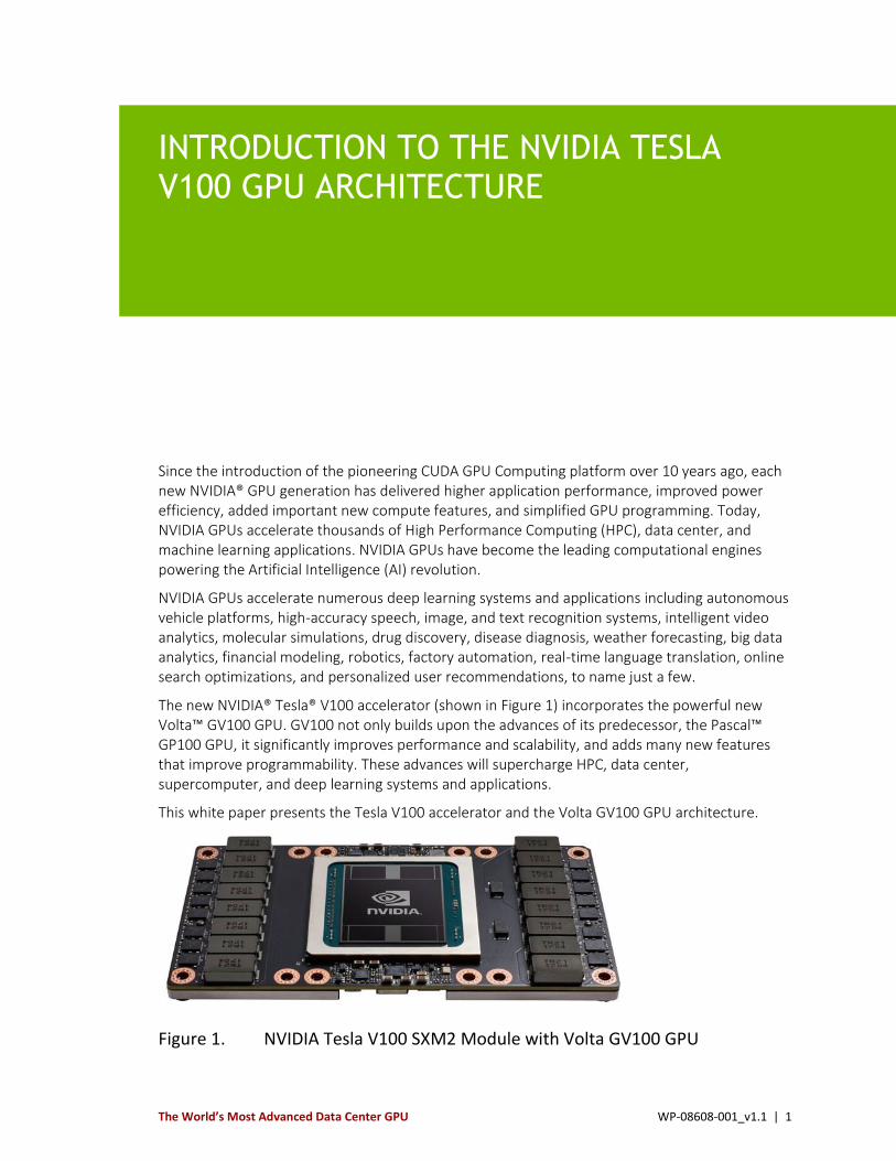
The new NVIDIA® Tesla® V100 accelerator (shown in Figure 1) incorporates the powerful new Volta™ GV100 GPU. GV100 not only builds upon the advances of its predecessor, the Pascal™ GP100 GPU, it significantly improves performance and scalability, and adds many new features that improve programmability. These advances will supercharge HPC, data center, supercomputer, and deep learning systems and applications.
This white paper presents the Tesla V100 accelerator and the Volta GV100 GPU architecture.
Figure 1. NVIDIA Tesla V100 SXM2 Module with Volta GV100 GPU

The World’s Most Advanced Data Center GPU WP-08608-001_v1.1 | 2
TESLA V100: THE AI COMPUTING AND HPC POWERHOUSE
The NVIDIA Tesla V100 accelerator is the world’s highest performing parallel processor, designed to power the most computationally intensive HPC, AI, and graphics workloads.
The GV100 GPU includes 21.1 billion transistors with a die size of 815 mm2. It is fabricated on a new TSMC 12 nm FFN (FinFET NVIDIA) high-performance manufacturing process customized for NVIDIA. GV100 delivers considerably more compute performance, and adds many new features compared to the prior Pascal GPU generation. Further simplifying GPU programming and application porting, GV100 also improves GPU resource utilization. GV100 is an extremely power-efficient processor, delivering exceptional performance per watt.
KEY FEATURES
Following are some key compute features of Tesla V100:
New Streaming Multiprocessor (SM) Architecture Optimized for Deep Learning Volta features a major new redesign of the SM processor architecture that is at the center of the GPU. The new Volta SM is 50% more energy efficient than the previous generation Pascal design, enabling major boosts in FP32 and FP64 performance in the same power envelope. New Tensor Cores designed specifically for deep learning deliver up to 12x higher peak TFLOPS for training and 6x higher peak TFLOPS for inference. With independent parallel integer and floating-point data paths, the Volta SM is also much more efficient on workloads with a mix of computation and addressing calculations. Volta’s new independent thread scheduling capability enables finer-grain synchronization and cooperation between parallel threads. Finally, a new combined L1 data cache and shared memory unit significantly improves performance while also simplifying programming.

Tesla V100: The AI Computing and HPC Powerhouse
The World’s Most Advanced Data Center GPU WP-08608-001_v1.1 | 3
Second-Generation NVIDIA NVLink™ The second generation of NVIDIA’s NVLink high-speed interconnect delivers higher bandwidth, more links, and improved scalability for multi-GPU and multi-GPU/CPU system configurations. Volta GV100 supports up to six NVLink links and total bandwidth of 300 GB/sec, compared to four NVLink links and 160 GB/s total bandwidth on GP100. NVLink now supports CPU mastering and cache coherence capabilities with IBM Power 9 CPU-based servers. The new NVIDIA DGX-1 with V100 AI supercomputer uses NVLink to deliver greater scalability for ultra-fast deep learning training.
HBM2 Memory: Faster, Higher Efficiency Volta’s highly tuned 16 GB HBM2 memory subsystem delivers 900 GB/sec peak memory bandwidth. The combination of both a new generation HBM2 memory from Samsung, and a new generation memory controller in Volta, provides 1.5x delivered memory bandwidth versus Pascal GP100, with up to 95% memory bandwidth utilization running many workloads.
Volta Multi-Process Service Volta Multi-Process Service (MPS) is a new feature of the Volta GV100 architecture providing hardware acceleration of critical components of the CUDA MPS server, enabling improved performance, isolation, and better quality of service (QoS) for multiple compute applications sharing the GPU. Volta MPS also triples the maximum number of MPS clients from 16 on Pascal to 48 on Volta.
Enhanced Unified Memory and Address Translation Services GV100 Unified Memory technology includes new access counters to allow more accurate migration of memory pages to the processor that accesses them most frequently, improving efficiency for memory ranges shared between processors. On IBM Power platforms, new Address Translation Services (ATS) support allows the GPU to access the CPU’s page tables directly.
Maximum Performance and Maximum Efficiency Modes In Maximum Performance mode, the Tesla V100 accelerator will operate up to its TDP (Thermal Design Power) level of 300 W to accelerate applications that require the fastest computational speed and highest data throughput. Maximum Efficiency Mode allows data center managers to tune power usage of their Tesla V100 accelerators to operate with optimal performance per watt. A not-to-exceed power cap can be set across all GPUs in a rack, reducing power consumption dramatically, while still obtaining excellent rack performance.
Cooperative Groups and New Cooperative Launch APIs Cooperative Groups is a new programming model introduced in CUDA 9 for organizing groups of communicating threads. Cooperative Groups allows developers to express the granularity at which threads are communicating, helping them to express richer, more efficient parallel decompositions. Basic Cooperative Groups functionality is supported on all NVIDIA GPUs since Kepler. Pascal and Volta include support for new cooperative launch APIs that support synchronization amongst CUDA thread blocks. Volta adds support for new synchronization patterns.

Tesla V100: The AI Computing and HPC Powerhouse
The World’s Most Advanced Data Center GPU WP-08608-001_v1.1 | 4
Volta Optimized Software New versions of deep learning frameworks such as Caffe2, MXNet, CNTK, TensorFlow, and others harness the performance of Volta to deliver dramatically faster training times and higher multi-node training performance. Volta-optimized versions of GPU accelerated libraries such as cuDNN, cuBLAS, and TensorRT leverage the new features of the Volta GV100 architecture to deliver higher performance for both deep learning inference and High Performance Computing (HPC) applications. The NVIDIA CUDA Toolkit version 9.0 includes new APIs and support for Volta features to provide even easier programmability.
Figure 2 shows the new technologies incorporated into the Tesla V100.
Figure 2. New Technologies in Tesla V100
Tesla V100: The AI Computing and HPC Powerhouse
The World’s Most Advanced Data Center GPU WP-08608-001_v1.1 | 5
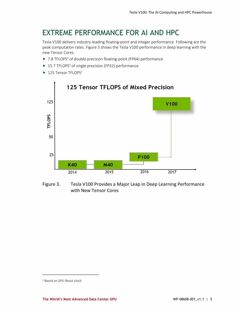
EXTREME PERFORMANCE FOR AI AND HPC Tesla V100 delivers industry-leading floating-point and integer performance. Following are the peak computation rates. Figure 3 shows the Tesla V100 performance in deep learning with the new Tensor Cores.
7.8 TFLOPS1 of double precision floating-point (FP64) performance
15.7 TFLOPS1 of single precision (FP32) performance
125 Tensor TFLOPS1
Figure 3. Tesla V100 Provides a Major Leap in Deep Learning Performance with New Tensor Cores
1 Based on GPU Boost clock.
The World’s Most Advanced Data Center GPU WP-08608-001_v1.1 | 6
NVIDIA GPUS THE FASTEST AND MOST FLEXIBLE DEEP LEARNING PLATFORM
Deep learning training and inferencing operations benefit greatly from GPU acceleration in both single-GPU and multi-GPU systems. NVIDIA Pascal GPUs have been used extensively to accelerate deep learning systems over the past year, and are significantly faster than CPUs for both training and inferencing. The new architectural features for deep learning combined with increased compute performance of the NVIDIA Tesla V100 GPU delivers increased neural network training and inference performance. In addition, multi-GPU systems with NVLink deliver tremendous performance scalability.
The flexible nature of GPU programmability allows new algorithms to be developed and deployed quickly. NVIDIA GPUs provide high performance, scalability, and programmability required to meet the continuing demands of AI and deep learning systems and algorithms for training and inferencing.
DEEP LEARNING BACKGROUND
Many different approaches have been used over the years to model human intelligence in the field of Artificial Intelligence. Machine Learning is a very popular approach to AI that train systems to learn how to make decisions and predict results on their own. Deep learning is a machine learning technique inspired by the neural learning process of the human brain. Deep learning uses deep neural networks (DNNs), so called because of their deep layering of many connected artificial neurons (sometimes called perceptrons), which can be trained with enormous amounts of input data to quickly solve complex problems with high accuracy. Once a neural network is trained, it can be deployed and used to identify and classify objects or patterns in a process known as inference. See Appendix C starting on page 44 in this paper for a high-level explanation of how a neural network operates.
Most neural networks consist of multiple layers of interconnected neurons. Each neuron and layer contributes towards the task that the network has been trained to execute. For example;
NVIDIA GPUs The Fastest and Most Flexible Deep Learning Platform
The World’s Most Advanced Data Center GPU WP-08608-001_v1.1 | 7
AlexNet, the Convolutional Neural Network (CNN) that won the 2012 ImageNet competition, consists of eight layers, 650,000 interconnected neurons, and almost 60 million parameters. Today, the complexity of neural networks has increased significantly, with recent networks such as deep residual networks (for example ResNet-152) having more than 150 layers, and millions more connected neurons and parameters.
GPU-ACCELERATED DEEP LEARNING
It is widely recognized within academia and industry that NVIDIA GPUs are the state-of-the-art engines for training deep neural networks due to both their speed and energy efficiency advantages compared to more traditional CPU-based platforms. Because neural networks are created from large numbers of identical neurons, they are highly parallel by nature. This parallelism maps naturally to GPUs, which provide a significant speedup over CPU-only training.
Neural networks rely heavily on matrix math operations, and complex multi-layered networks require tremendous amounts of floating-point performance and bandwidth for both efficiency and speed. GPUs have thousands of processing cores optimized for matrix math operations, providing tens to hundreds of TFLOPS of performance. GPUs are the obvious computing platform for deep neural network-based artificial intelligence and machine learning applications.
Volta's architecture is highly specialized for running deep learning workloads, achieving a tremendous increase in performance within the same power budget as the previous generation architecture. Technical details of how this was accomplished are described in the architecture sections below.
The World’s Most Advanced Data Center GPU WP-08608-001_v1.1 | 8
GV100 GPU HARDWARE ARCHITECTURE IN-DEPTH
The NVIDIA Tesla V100 accelerator, featuring the Volta GV100 GPU, is the highest-performing parallel computing processor in the world today. GV100 has significant new hardware innovations that provide tremendous speedups for deep learning algorithms and frameworks, in addition to providing far more computational horsepower for HPC systems and applications.
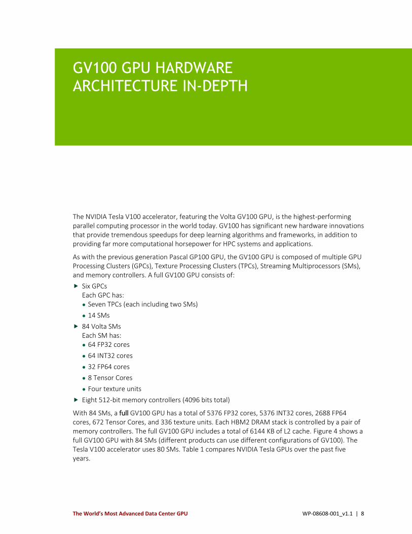
As with the previous generation Pascal GP100 GPU, the GV100 GPU is composed of multiple GPU Processing Clusters (GPCs), Texture Processing Clusters (TPCs), Streaming Multiprocessors (SMs), and memory controllers. A full GV100 GPU consists of:
Six GPCs Each GPC has: ● Seven TPCs (each including two SMs)
● 14 SMs
84 Volta SMs Each SM has: ● 64 FP32 cores
● 64 INT32 cores
● 32 FP64 cores
● 8 Tensor Cores
● Four texture units
Eight 512-bit memory controllers (4096 bits total)
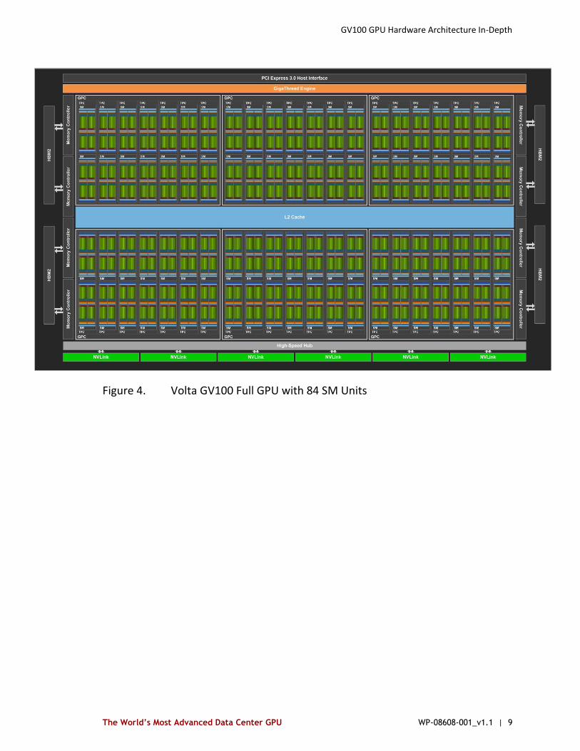
With 84 SMs, a full GV100 GPU has a total of 5376 FP32 cores, 5376 INT32 cores, 2688 FP64 cores, 672 Tensor Cores, and 336 texture units. Each HBM2 DRAM stack is controlled by a pair of memory controllers. The full GV100 GPU includes a total of 6144 KB of L2 cache. Figure 4 shows a full GV100 GPU with 84 SMs (different products can use different configurations of GV100). The Tesla V100 accelerator uses 80 SMs. Table 1 compares NVIDIA Tesla GPUs over the past five years.
GV100 GPU Hardware Architecture In-Depth
The World’s Most Advanced Data Center GPU WP-08608-001_v1.1 | 9
Figure 4. Volta GV100 Full GPU with 84 SM Units
GV100 GPU Hardware Architecture In-Depth
The World’s Most Advanced Data Center GPU WP-08608-001_v1.1 | 10
Table 1. Comparison of NVIDIA Tesla GPUs
Tesla Product Tesla K40 Tesla M40 Tesla P100 Tesla V100
GPU GK180 (Kepler) GM200 (Maxwell) GP100 (Pascal) GV100 (Volta)
SMs 15 24 56 80
TPCs 15 24 28 40
FP32 Cores / SM 192 128 64 64
FP32 Cores / GPU 2880 3072 3584 5120
FP64 Cores / SM 64 4 32 32
FP64 Cores / GPU 960 96 1792 2560
Tensor Cores / SM NA NA NA 8
Tensor Cores / GPU NA NA NA 640
GPU Boost Clock 810/875 MHz 1114 MHz 1480 MHz 1530 MHz
Peak FP32 TFLOPS1 5 6.8 10.6 15.7
Peak FP64 TFLOPS1 1.7 .21 5.3 7.8
Peak Tensor TFLOPS1 NA NA NA 125
Texture Units 240 192 224 320
Memory Interface 384-bit GDDR5 384-bit GDDR5 4096-bit HBM2 4096-bit HBM2
Memory Size Up to 12 GB Up to 24 GB 16 GB 16 GB
L2 Cache Size 1536 KB 3072 KB 4096 KB 6144 KB
Shared Memory Size / SM
16 KB/32 KB/48 KB
96 KB 64 KB Configurable up to 96 KB
Register File Size / SM 256 KB 256 KB 256 KB 256KB
Register File Size / GPU
3840 KB 6144 KB 14336 KB 20480 KB
TDP 235 Watts 250 Watts 300 Watts 300 Watts
Transistors 7.1 billion 8 billion 15.3 billion 21.1 billion
GPU Die Size 551 mm² 601 mm² 610 mm² 815 mm²
Manufacturing Process
28 nm 28 nm 16 nm FinFET+ 12 nm FFN
1 Peak TFLOPS rates are based on GPU Boost Clock
GV100 GPU Hardware Architecture In-Depth
The World’s Most Advanced Data Center GPU WP-08608-001_v1.1 | 11
EXTREME PERFORMANCE AND HIGH EFFICIENCY
With each new generation, NVIDIA develops significantly higher performing GPUs that also improve energy efficiency. Tesla V100 gives data center architects a new dimension of design flexibility, and it can be configured to deliver either absolute maximum performance, or most energy efficient performance. In Tesla V100, these two modes of operation are called Maximum Performance Mode and Maximum Efficiency Mode.
In Maximum Performance mode, the Tesla V100 accelerator operates up to its TDP level of 300 W to accelerate applications that require the fastest computational speed and highest data throughput.
Maximum Efficiency Mode is an operating mode that enables data center managers to run their Tesla V100 accelerators with optimal performance per watt. The V100 can be set to run at a point on the power/performance curve that yields the best performance with the highest power efficiency. For example, the most efficient range on the curve might be 50-60% of TDP, where the GPU can still attain 75-85% of maximum performance. Data center managers can set a not-to-exceed power cap across all GPUs in a rack, reducing power consumption dramatically, while still obtaining excellent performance. This capability allows data center designers to maximize per-rack performance within that rack’s power budget. In some cases, this optimization could even enable additional server nodes in the rack.
The power limit can be set by NVIDIA-SMI (a command-line utility that can be used by the data center manager) or using NVML (a C-based API library that exposes power limit controls that Tesla OEM partners can integrate with their toolset). Maximum Efficiency Mode does not lower peak clock or memory clock during normal operation, rather the GPU works to attain the highest clock speed residency possible within the specified power limit. Many workloads do not consume the entire 300 W TDP of the Tesla V100, so a higher power limit may be possible in some cases. However, data center designers should set GPU power levels based on heaviest expected workloads so their rack power budget is not exceeded.
GV100 GPU Hardware Architecture In-Depth
The World’s Most Advanced Data Center GPU WP-08608-001_v1.1 | 12
VOLTA STREAMING MULTIPROCESSOR
Volta features a new Streaming Multiprocessor (SM) architecture that delivers major improvements in performance, energy efficiency, and ease of programmability.
Major Features include:
New mixed-precision Tensor Cores purpose-built for deep learning matrix arithmetic, delivering 12x TFLOPS for training, compared to GP100, in the same power envelope
50% higher energy efficiency on general compute workloads
Enhanced high performance L1 data cache
A new SIMT thread model that removes limitations present in previous SIMT and SIMD processor designs
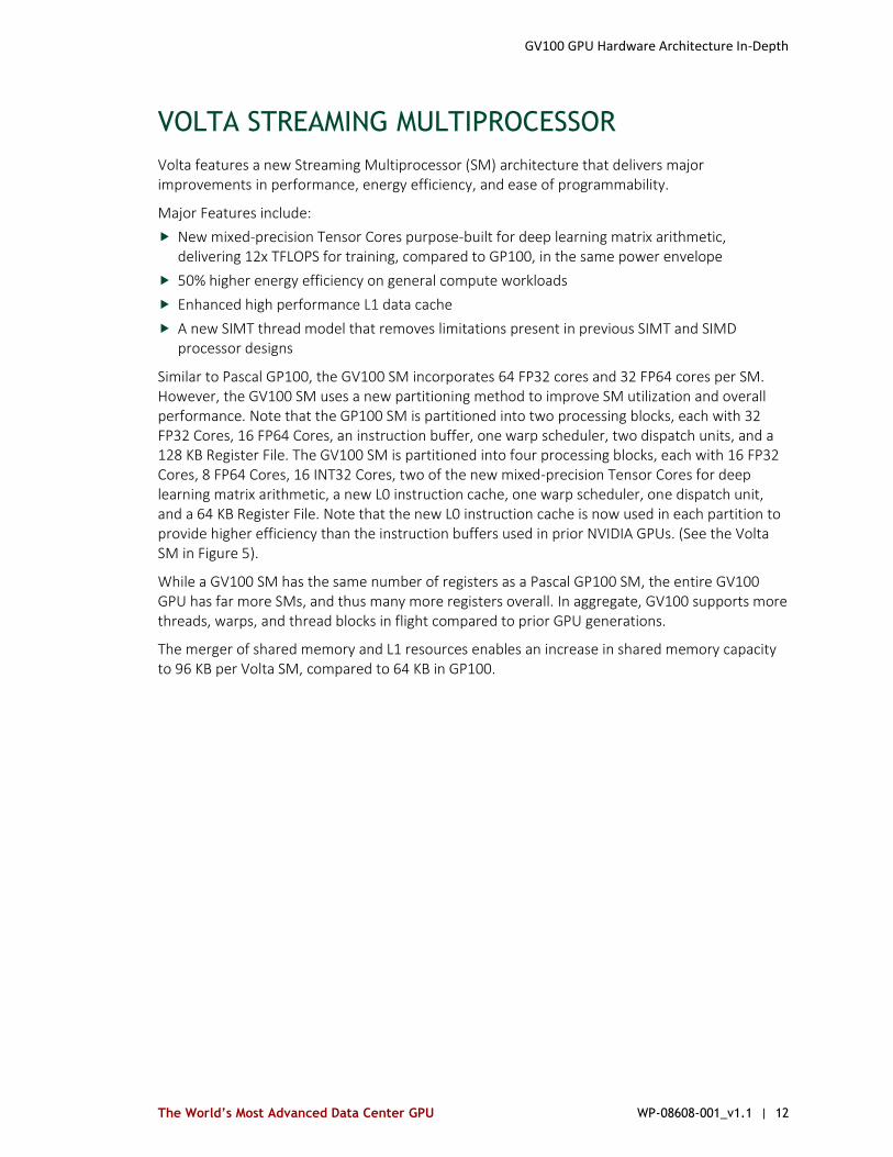
Similar to Pascal GP100, the GV100 SM incorporates 64 FP32 cores and 32 FP64 cores per SM. However, the GV100 SM uses a new partitioning method to improve SM utilization and overall performance. Note that the GP100 SM is partitioned into two processing blocks, each with 32 FP32 Cores, 16 FP64 Cores, an instruction buffer, one warp scheduler, two dispatch units, and a 128 KB Register File. The GV100 SM is partitioned into four processing blocks, each with 16 FP32 Cores, 8 FP64 Cores, 16 INT32 Cores, two of the new mixed-precision Tensor Cores for deep learning matrix arithmetic, a new L0 instruction cache, one warp scheduler, one dispatch unit, and a 64 KB Register File. Note that the new L0 instruction cache is now used in each partition to provide higher efficiency than the instruction buffers used in prior NVIDIA GPUs. (See the Volta SM in Figure 5).
While a GV100 SM has the same number of registers as a Pascal GP100 SM, the entire GV100 GPU has far more SMs, and thus many more registers overall. In aggregate, GV100 supports more threads, warps, and thread blocks in flight compared to prior GPU generations.
The merger of shared memory and L1 resources enables an increase in shared memory capacity to 96 KB per Volta SM, compared to 64 KB in GP100.
GV100 GPU Hardware Architecture In-Depth
The World’s Most Advanced Data Center GPU WP-08608-001_v1.1 | 13
Figure 5. Volta GV100 Streaming Multiprocessor (SM)
GV100 GPU Hardware Architecture In-Depth
The World’s Most Advanced Data Center GPU WP-08608-001_v1.1 | 14
Tensor Cores
Tesla P100 delivered considerably higher performance for training neural networks compared to the prior generation NVIDIA Maxwell and Kepler architectures, but the complexity and size of neural networks have continued to grow. As mentioned, new networks with thousands of layers and millions of neurons demand even higher performance and faster training times.
New Tensor Cores are a key capability enabling the Volta GV100 GPU architecture to deliver the performance required to train large neural networks.
The Tesla V100 GPU contains 640 Tensor Cores: eight (8) per SM and two (2) per each processing block (partition) within an SM. In Volta GV100, each Tensor Core performs 64 floating point FMA operations per clock, and eight Tensor Cores in an SM perform a total of 512 FMA operations (or 1024 individual floating point operations) per clock.
Tesla V100’s Tensor Cores deliver up to 125 Tensor TFLOPS for training and inference applications. Tensor Cores provide up to 12x higher peak TFLOPS on Tesla V100 that can be applied to deep learning training compared to using standard FP32 operations on P100. For deep learning inference, V100 Tensor Cores provide up to 6x higher peak TFLOPS compared to standard FP16 operations on P100.
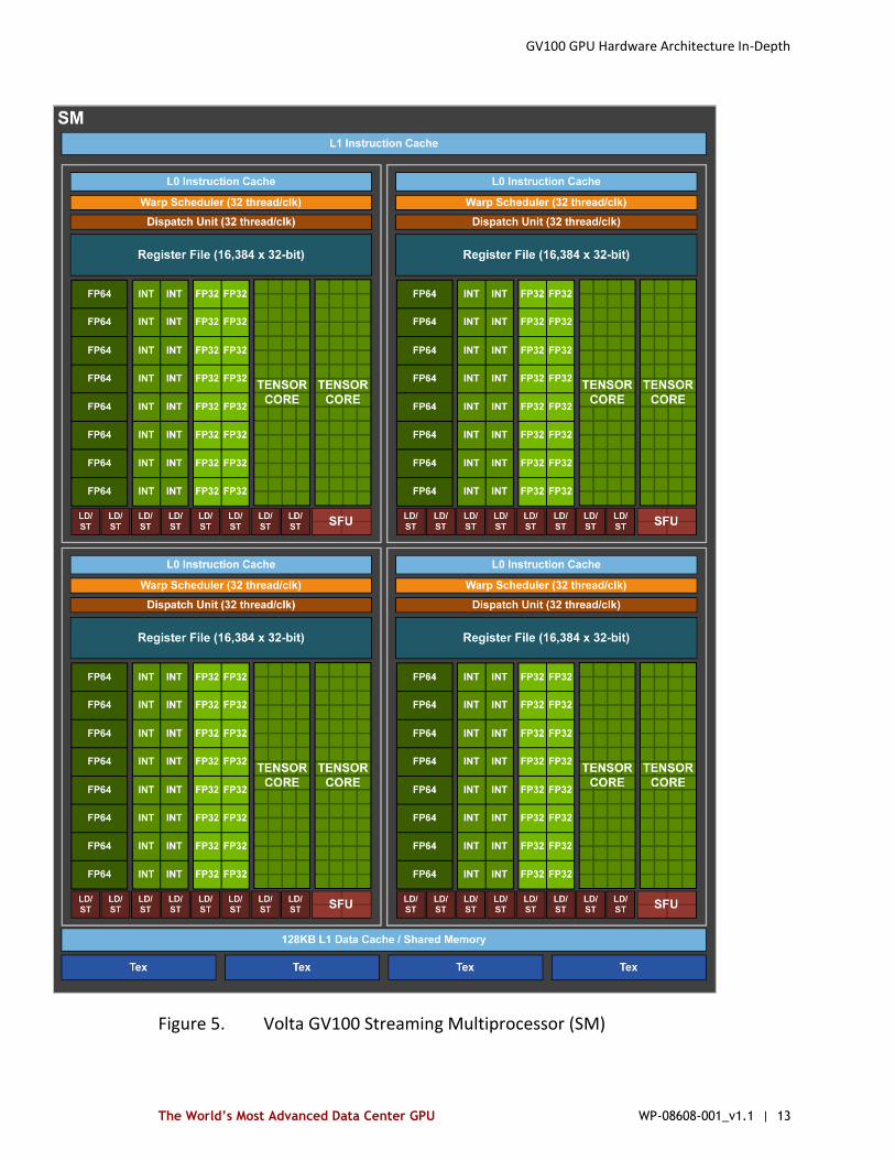
Matrix-Matrix multiplication (GEMM) operations are at the core of neural network training and inferencing, and are used to multiply large matrices of input data and weights in the connected layers of the network. For applications that use single precision matrix multiplication, Figure 6 shows that Tesla V100 with CUDA 9 delivers up to 1.8x higher performance than Tesla P100 with CUDA 8. For matrix multiplication with half-precision inputs for training and inference operations, Figure 7 shows that for the case of matrix operations with FP16 inputs and FP32 accumulation, Volta’s mixed-precision Tensor Cores boost performance by more than 9x compared to P100.
Figure 6. cuBLAS Single Precision (FP32)
Single-precision (FP32) Matrix-Matrix Multiplies are up to 1.8x faster on Tesla V100 with CUDA 9 than on Tesla P100 with CUDA 8

GV100 GPU Hardware Architecture In-Depth
The World’s Most Advanced Data Center GPU WP-08608-001_v1.1 | 15
Figure 7. cuBLAS Mixed Precision (FP16 Input, FP32 Compute)
Tensor Cores and their associated data paths are custom-designed to dramatically increase floating-point compute throughput with high energy efficiency.
Each Tensor Core operates on a 4x4 matrix and performs the following operation:
D = A×B + C
where A, B, C, and D are 4x4 matrices (Figure 8). The matrix multiply inputs A and B are FP16 matrices, while the accumulation matrices C and D may be FP16 or FP32 matrices (see Figure 8).
Figure 8. Tensor Core 4x4 Matrix Multiply and Accumulate
Tensor Cores operate on FP16 input data with FP32 accumulation. The FP16 multiply results in a full precision product that is then accumulated using FP32 addition with the other intermediate products for a 4x4x4 matrix multiply (see Figure 9). In practice, Tensor Cores are used to perform much larger 2D or higher dimensional matrix operations, built up from these smaller elements.
Mixed Precision Matrix-Matrix Multiplies are over 9x faster on Tesla V100 with CUDA 9 compared to FP32 matrix multiplies on Tesla P100 with CUDA 8
GV100 GPU Hardware Architecture In-Depth
The World’s Most Advanced Data Center GPU WP-08608-001_v1.1 | 16
Figure 9. Mixed Precision Multiply and Accumulate in Tensor Core
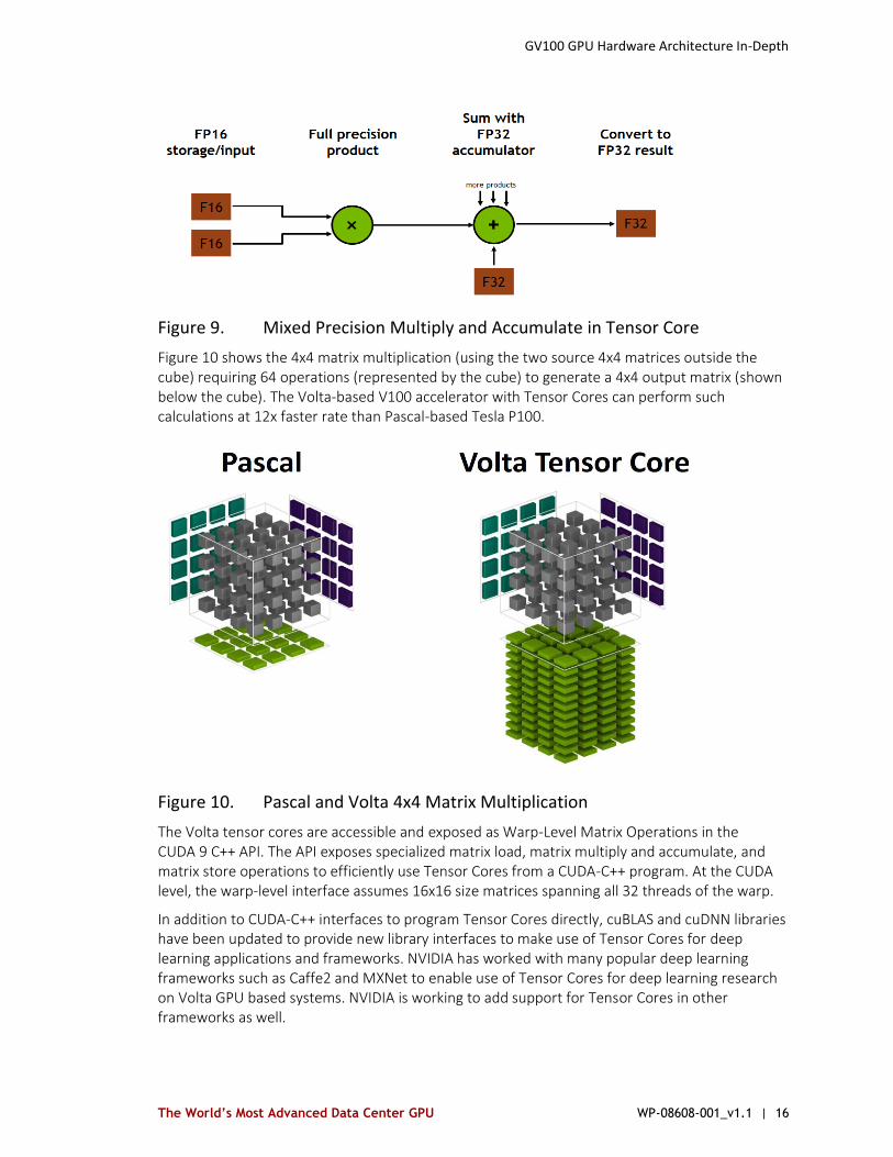
Figure 10 shows the 4x4 matrix multiplication (using the two source 4x4 matrices outside the cube) requiring 64 operations (represented by the cube) to generate a 4x4 output matrix (shown below the cube). The Volta-based V100 accelerator with Tensor Cores can perform such calculations at 12x faster rate than Pascal-based Tesla P100.
Figure 10. Pascal and Volta 4x4 Matrix Multiplication
The Volta tensor cores are accessible and exposed as Warp-Level Matrix Operations in the CUDA 9 C++ API. The API exposes specialized matrix load, matrix multiply and accumulate, and matrix store operations to efficiently use Tensor Cores from a CUDA-C++ program. At the CUDA level, the warp-level interface assumes 16x16 size matrices spanning all 32 threads of the warp.
In addition to CUDA-C++ interfaces to program Tensor Cores directly, cuBLAS and cuDNN libraries have been updated to provide new library interfaces to make use of Tensor Cores for deep learning applications and frameworks. NVIDIA has worked with many popular deep learning frameworks such as Caffe2 and MXNet to enable use of Tensor Cores for deep learning research on Volta GPU based systems. NVIDIA is working to add support for Tensor Cores in other frameworks as well.
GV100 GPU Hardware Architecture In-Depth
The World’s Most Advanced Data Center GPU WP-08608-001_v1.1 | 17
Enhanced L1 Data Cache and Shared Memory
The new combined L1 data cache and shared memory subsystem of the Volta SM significantly improves performance while also simplifying programming and reducing the tuning required to attain at or near-peak application performance.
Combining data cache and shared memory functionality into a single memory block provides the best overall performance for both types of memory accesses. The combined capacity is 128 KB/SM, more than seven times larger than the GP100 data cache, and all of it is usable as a cache by programs that do not use shared memory. Texture units also use the cache. For example, if shared memory is configured to 64 KB, texture and load/store operations can use the remaining 64 KB of L1.
Integration within the shared memory block ensures the Volta GV100 L1 cache has much lower latency and higher bandwidth than the L1 caches in past NVIDIA GPUs. The L1 In Volta functions as a high-throughput conduit for streaming data while simultaneously providing high-bandwidth and low-latency access to frequently reused data—the best of both worlds. This combination is unique to Volta and delivers more accessible performance than in the past.
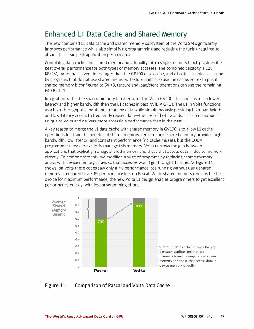
A key reason to merge the L1 data cache with shared memory in GV100 is to allow L1 cache operations to attain the benefits of shared memory performance. Shared memory provides high bandwidth, low latency, and consistent performance (no cache misses), but the CUDA programmer needs to explicitly manage this memory. Volta narrows the gap between applications that explicitly manage shared memory and those that access data in device memory directly. To demonstrate this, we modified a suite of programs by replacing shared memory arrays with device memory arrays so that accesses would go through L1 cache. As Figure 11 shows, on Volta these codes saw only a 7% performance loss running without using shared memory, compared to a 30% performance loss on Pascal. While shared memory remains the best choice for maximum performance, the new Volta L1 design enables programmers to get excellent performance quickly, with less programming effort.
Figure 11. Comparison of Pascal and Volta Data Cache
Volta’s L1 data cache narrows the gap between applications that are manually tuned to keep data in shared memory and those that access data in device memory directly.
GV100 GPU Hardware Architecture In-Depth
The World’s Most Advanced Data Center GPU WP-08608-001_v1.1 | 18
The GV100 L1 cache improves performance in a variety of situations where shared memory is not the best choice or is unable to work. With Volta GV100, the merging of shared memory and L1 delivers a high-speed path to global memory capable of streaming access with unlimited cache-misses in flight. Prior NVIDIA GPUs only performed load caching, while GV100 introduces write-caching (caching of store operations) to further improve performance.
Simultaneous Execution of FP32 and INT32 Operations
Unlike Pascal GPUs, which could not execute FP32 and INT32 instructions simultaneously, the Volta GV100 SM includes separate FP32 and INT32 cores, allowing simultaneous execution of FP32 and INT32 operations at full throughput, while also increasing instruction issue throughput. Dependent instruction issue latency is also reduced for core FMA (Fused Multiply-Add) math operations, requiring only four clock cycles on Volta, compared to six cycles on Pascal.
Many applications have inner loops that perform pointer arithmetic (integer memory address calculations) combined with floating-point computations that will benefit from simultaneous execution of FP32 and INT32 instructions. Each iteration of a pipelined loop can update addresses (INT32 pointer arithmetic) and load data for the next iteration while simultaneously processing the current iteration in FP32.
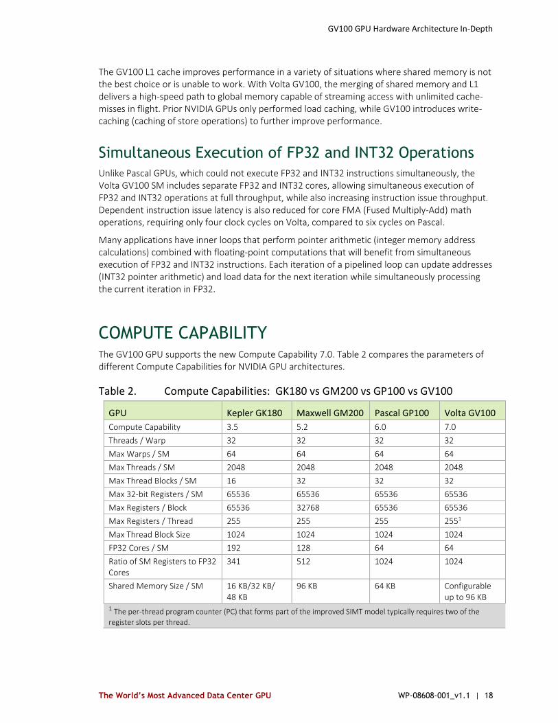
COMPUTE CAPABILITY The GV100 GPU supports the new Compute Capability 7.0. Table 2 compares the parameters of different Compute Capabilities for NVIDIA GPU architectures.
Table 2. Compute Capabilities: GK180 vs GM200 vs GP100 vs GV100
GPU Kepler GK180 Maxwell GM200 Pascal GP100 Volta GV100
Compute Capability 3.5 5.2 6.0 7.0
Threads / Warp 32 32 32 32
Max Warps / SM 64 64 64 64
Max Threads / SM 2048 2048 2048 2048
Max Thread Blocks / SM 16 32 32 32
Max 32-bit Registers / SM 65536 65536 65536 65536
Max Registers / Block 65536 32768 65536 65536
Max Registers / Thread 255 255 255 2551
Max Thread Block Size 1024 1024 1024 1024
FP32 Cores / SM 192 128 64 64
Ratio of SM Registers to FP32 Cores
341 512 1024 1024
Shared Memory Size / SM 16 KB/32 KB/ 48 KB
96 KB 64 KB Configurable up to 96 KB
1 The per-thread program counter (PC) that forms part of the improved SIMT model typically requires two of the
register slots per thread.

GV100 GPU Hardware Architecture In-Depth
The World’s Most Advanced Data Center GPU WP-08608-001_v1.1 | 19
NVLINK: HIGHER BANDWIDTH, MORE LINKS, MORE FEATURES
NVLink is NVIDIA’s high-speed interconnect technology first introduced in 2016 with the Tesla P100 accelerator and Pascal GP100 GPU. NVLink provides significantly more performance for both GPU-to-GPU and GPU-to-CPU system configurations compared to using PCIe interconnects. Refer to the Pascal Architecture Whitepaper for basic details on NVLink technology. Tesla V100 introduces the second generation of NVLink, which provides higher link speeds, more links per GPU, CPU mastering, cache coherence, and scalability improvements.
More Links, Faster Links
Systems with multiple GPUs and CPUs are becoming common in a variety of industries as developers expose and leverage more parallelism in applications such as AI computing. This trend escalates the need for a faster and more scalable multiprocessor interconnect. Similarly, high-performance GPU-accelerated systems with tens to many thousands of compute nodes are being deployed in data centers, research facilities, and supercomputers to solve ever larger problems. NVIDIA’s own DGX-1 systems with P100 and V100 incorporate NVLink technology. In 2016, NVIDIA worked closely with IBM to build high-performance servers using both NVIDIA Pascal GPUs and IBM Power 8+ CPUs. Today, NVIDIA is working with IBM to build even higher performance servers using Tesla V100 accelerators and Power 9 CPUs connected with NVLink.
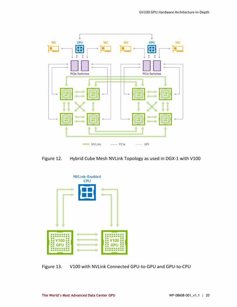
Compared to NVLink on Pascal, NVLink on V100 increases the signaling rate from 20 to 25 Gigabits/second. Each link now provides 25 Gigabytes/second in each direction. The number of links supported has been increased from four to six pushing the supported GPU NVLink bandwidth to 300 Gigabytes/second. The links can be used exclusively for GPU-to-GPU communication as in the DGX-1 with V100 topology shown in Figure 12, or some combination of GPU-to-GPU and GPU-to-CPU communication as shown in Figure 13.
More Features
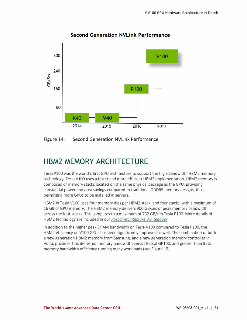
The second generation of NVLink allows direct load/store/atomic access from the CPU to each GPU’s HBM2 memory. Coupled with a new CPU mastering capability, NVLink supports coherency operations allowing data reads from graphics memory to be stored in the CPU’s cache hierarchy. The lower latency of access from the CPU’s cache is key for CPU performance. While P100 supported peer GPU atomics, sending GPU atomics across NVLink and completed at the target CPU was not supported. NVLink adds support for atomics initiated by either the GPU or the CPU. Support for Address Translation Services (ATS) has been added allowing the GPU to access the CPU’s page tables directly. A low-power mode of operation for the link has been added allowing for significant power savings when the link is not being heavily used (see Figure 14).
The increased number of links, faster link speed, and enhanced functionality of second-generation NVLink, combined with Volta’s new Tensor Cores, results in significant increases in deep learning performance in multi-GPU Tesla V100 systems over systems with Tesla P100 GPUs.
GV100 GPU Hardware Architecture In-Depth
The World’s Most Advanced Data Center GPU WP-08608-001_v1.1 | 20
Figure 12. Hybrid Cube Mesh NVLink Topology as used in DGX-1 with V100
Figure 13. V100 with NVLink Connected GPU-to-GPU and GPU-to-CPU
GV100 GPU Hardware Architecture In-Depth
The World’s Most Advanced Data Center GPU WP-08608-001_v1.1 | 21
Figure 14. Second Generation NVLink Performance
HBM2 MEMORY ARCHITECTURE
Tesla P100 was the world’s first GPU architecture to support the high-bandwidth HBM2 memory technology. Tesla V100 uses a faster and more efficient HBM2 implementation. HBM2 memory is composed of memory stacks located on the same physical package as the GPU, providing substantial power and area savings compared to traditional GDDR5 memory designs, thus permitting more GPUs to be installed in servers.
HBM2 in Tesla V100 uses four memory dies per HBM2 stack, and four stacks, with a maximum of 16 GB of GPU memory. The HBM2 memory delivers 900 GB/sec of peak memory bandwidth across the four stacks. This compares to a maximum of 732 GB/s in Tesla P100. More details of HBM2 technology are included in our Pascal Architecture Whitepaper.
In addition to the higher peak DRAM bandwidth on Tesla V100 compared to Tesla P100, the HBM2 efficiency on V100 GPUs has been significantly improved as well. The combination of both a new generation HBM2 memory from Samsung, and a new generation memory controller in Volta, provides 1.5x delivered memory bandwidth versus Pascal GP100, and greater than 95% memory bandwidth efficiency running many workloads (see Figure 15).

GV100 GPU Hardware Architecture In-Depth
The World’s Most Advanced Data Center GPU WP-08608-001_v1.1 | 22
Figure 15. HBM2 Memory Speedup on V100 vs P100
ECC Memory Resiliency
The Tesla V100 HBM2 memory subsystem supports Single-Error Correcting Double-Error Detecting (SECDED) Error Correction Code (ECC) to protect data. ECC provides higher reliability for compute applications that are sensitive to data corruption. It is especially important in large-scale cluster computing environments where GPUs process very large datasets and/or run applications for extended periods.
HBM2 supports native or sideband ECC where a small memory region, separate from main memory, is used for ECC bits. This compares to inline ECC where a portion of main memory is carved out for ECC bits, as in the GDDR5 memory subsystem of the Tesla K40 GPU where 6.25% of the overall GDDR5 is reserved for ECC bits. With V100 and P100, ECC can be active without a bandwidth or capacity penalty. For memory writes, the ECC bits are calculated across 32 bytes of data in a write request. Eight ECC bits are created for each eight bytes of data. For memory reads, the 32 ECC bits are read in parallel with each 32-byte read of data. ECC bits are used to correct single bit errors or flag double bit errors.
Other key structures in GV100 are also protected by SECDED ECC, including the SM register file, L1 cache, and L2 cache. The same SECDED ECC protection was provided across the same structures in Pascal GP100 to ensure a high level of error detection and correction, and overall memory resiliency.
GV100 GPU Hardware Architecture In-Depth
The World’s Most Advanced Data Center GPU WP-08608-001_v1.1 | 23
COPY ENGINE ENHANCEMENTS
NVIDIA GPU copy engines transfer data between multiple GPUs or between GPUs and CPUs. In prior GPUs, performing copy engine transfers (which are like DMA transfers) could cause fatal faults if either the source or destination memory addresses were not mapped in the GPU page tables. The prior copy engines required both source and destination memory regions to be pinned (non-pageable).
The new Volta GV100 GPU copy engines can generate page faults for addresses that are not mapped into the page tables. The memory subsystem can then service the page faults, mapping the addresses into the page table, after which the copy engine can perform the transfer. This is an important enhancement, especially in large multi-GPU / multi-CPU systems, because pinning memory for multiple copy engine operations between multiple processors can substantially reduce available memory. With hardware page faulting, addresses can be passed to the copy engines without worrying if they are resident, and the copy process just works. This feature may be used in ATS systems today.
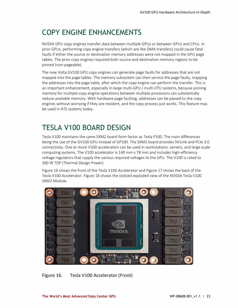
TESLA V100 BOARD DESIGN Tesla V100 maintains the same SXM2 board form factor as Tesla P100. The main differences being the use of the GV100 GPU instead of GP100. The SXM2 board provides NVLink and PCIe 3.0 connectivity. One or more V100 accelerators can be used in workstations, servers, and large-scale computing systems. The V100 accelerator is 140 mm x 78 mm and includes high-efficiency voltage regulators that supply the various required voltages to the GPU. The V100 is rated to 300 W TDP (Thermal Design Power).
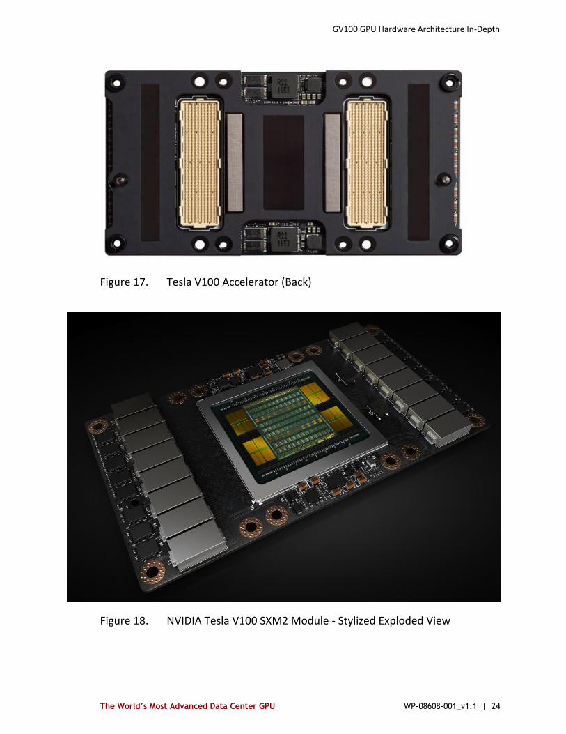
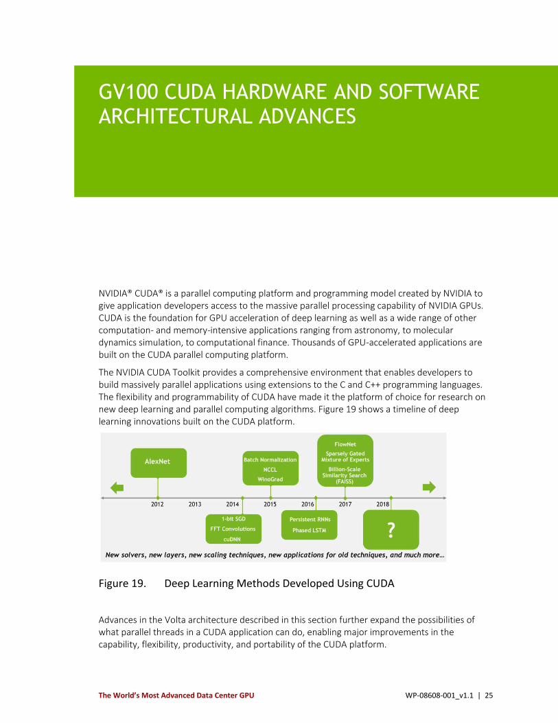
Figure 16 shows the front of the Tesla V100 Accelerator and Figure 17 shows the back of the Tesla V100 Accelerator. Figure 18 shows the stylized exploded view of the NVIDIA Tesla V100 SXM2 Module.
Figure 16. Tesla V100 Accelerator (Front)
GV100 GPU Hardware Architecture In-Depth
The World’s Most Advanced Data Center GPU WP-08608-001_v1.1 | 24
Figure 17. Tesla V100 Accelerator (Back)
Figure 18. NVIDIA Tesla V100 SXM2 Module - Stylized Exploded View
The World’s Most Advanced Data Center GPU WP-08608-001_v1.1 | 25
GV100 CUDA HARDWARE AND SOFTWARE ARCHITECTURAL ADVANCES
NVIDIA® CUDA® is a parallel computing platform and programming model created by NVIDIA to give application developers access to the massive parallel processing capability of NVIDIA GPUs. CUDA is the foundation for GPU acceleration of deep learning as well as a wide range of other computation- and memory-intensive applications ranging from astronomy, to molecular dynamics simulation, to computational finance. Thousands of GPU-accelerated applications are built on the CUDA parallel computing platform.
The NVIDIA CUDA Toolkit provides a comprehensive environment that enables developers to build massively parallel applications using extensions to the C and C++ programming languages. The flexibility and programmability of CUDA have made it the platform of choice for research on new deep learning and parallel computing algorithms. Figure 19 shows a timeline of deep learning innovations built on the CUDA platform.
Figure 19. Deep Learning Methods Developed Using CUDA
Advances in the Volta architecture described in this section further expand the possibilities of what parallel threads in a CUDA application can do, enabling major improvements in the capability, flexibility, productivity, and portability of the CUDA platform.
GV100 CUDA Hardware and Software Architectural Advances
The World’s Most Advanced Data Center GPU WP-08608-001_v1.1 | 26
INDEPENDENT THREAD SCHEDULING
The Volta architecture is designed to be significantly easier to program than prior GPUs, enabling users to work productively on more complex and diverse applications. Volta GV100 is the first GPU to support independent thread scheduling, which enables finer-grain synchronization and cooperation between parallel threads in a program. One of the major design goals for Volta was to reduce the effort required to get programs running on the GPU, and to enable greater flexibility in thread cooperation, leading to higher efficiency for fine-grained parallel algorithms.
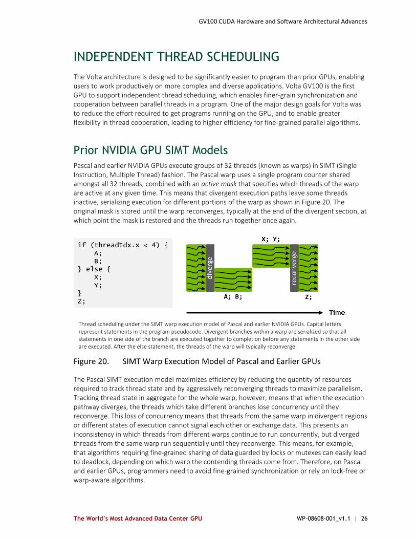
Prior NVIDIA GPU SIMT Models
Pascal and earlier NVIDIA GPUs execute groups of 32 threads (known as warps) in SIMT (Single Instruction, Multiple Thread) fashion. The Pascal warp uses a single program counter shared amongst all 32 threads, combined with an active mask that specifies which threads of the warp are active at any given time. This means that divergent execution paths leave some threads inactive, serializing execution for different portions of the warp as shown in Figure 20. The original mask is stored until the warp reconverges, typically at the end of the divergent section, at which point the mask is restored and the threads run together once again.
Figure 20. SIMT Warp Execution Model of Pascal and Earlier GPUs
The Pascal SIMT execution model maximizes efficiency by reducing the quantity of resources required to track thread state and by aggressively reconverging threads to maximize parallelism. Tracking thread state in aggregate for the whole warp, however, means that when the execution pathway diverges, the threads which take different branches lose concurrency until they reconverge. This loss of concurrency means that threads from the same warp in divergent regions or different states of execution cannot signal each other or exchange data. This presents an inconsistency in which threads from different warps continue to run concurrently, but diverged threads from the same warp run sequentially until they reconverge. This means, for example, that algorithms requiring fine-grained sharing of data guarded by locks or mutexes can easily lead to deadlock, depending on which warp the contending threads come from. Therefore, on Pascal and earlier GPUs, programmers need to avoid fine-grained synchronization or rely on lock-free or warp-aware algorithms.
Thread scheduling under the SIMT warp execution model of Pascal and earlier NVIDIA GPUs. Capital letters represent statements in the program pseudocode. Divergent branches within a warp are serialized so that all statements in one side of the branch are executed together to completion before any statements in the other side are executed. After the else statement, the threads of the warp will typically reconverge.

GV100 CUDA Hardware and Software Architectural Advances
The World’s Most Advanced Data Center GPU WP-08608-001_v1.1 | 27
Volta SIMT Model
Volta transforms this picture by enabling equal concurrency between all threads, regardless of warp. It does this by maintaining execution state per thread, including a program counter and call stack, as shown in Figure 21.
Figure 21. Volta Warp with Per-Thread Program Counter and Call Stack
Volta’s independent thread scheduling allows the GPU to yield execution of any thread, either to make better use of execution resources or to allow one thread to wait for data to be produced by another. To maximize parallel efficiency, Volta includes a schedule optimizer which determines how to group active threads from the same warp together into SIMT units. This retains the high throughput of SIMT execution as in prior NVIDIA GPUs, but with much more flexibility: threads can now diverge and reconverge at sub-warp granularity, while the convergence optimizer in Volta will still group together threads which are executing the same code and run them in parallel for maximum efficiency
Execution of the code example from Figure 20 looks somewhat different on Volta. Statements from the if and else branches in the program can now be interleaved in time as shown in Figure 22. Note that execution is still SIMT: at any given clock cycle, CUDA cores execute the same instruction for all active threads in a warp just as before, retaining the execution efficiency of previous architectures. Importantly, Volta’s ability to independently schedule threads within a warp makes it possible to implement complex, fine-grained algorithms and data structures in a more natural way. While the scheduler supports independent execution of threads, it optimizes non-synchronizing code to maintain as much convergence as possible for maximum SIMT efficiency.
Volta (bottom) independent thread scheduling architecture block diagram compared to Pascal and earlier architectures (top). Volta maintains per-thread scheduling resources such as program counter (PC) and call stack (S), while earlier architectures maintained these resources per warp.
GV100 CUDA Hardware and Software Architectural Advances
The World’s Most Advanced Data Center GPU WP-08608-001_v1.1 | 28
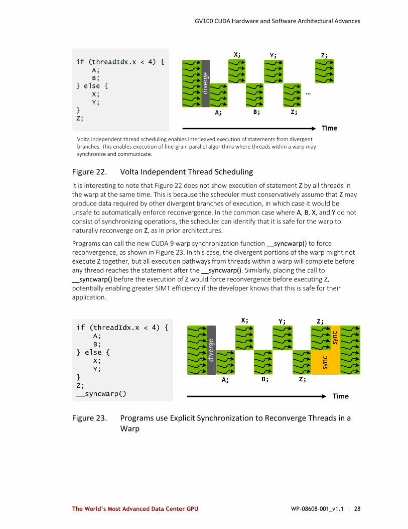
Figure 22. Volta Independent Thread Scheduling
It is interesting to note that Figure 22 does not show execution of statement Z by all threads in the warp at the same time. This is because the scheduler must conservatively assume that Z may produce data required by other divergent branches of execution, in which case it would be unsafe to automatically enforce reconvergence. In the common case where A, B, X, and Y do not consist of synchronizing operations, the scheduler can identify that it is safe for the warp to naturally reconverge on Z, as in prior architectures.
Programs can call the new CUDA 9 warp synchronization function __syncwarp() to force reconvergence, as shown in Figure 23. In this case, the divergent portions of the warp might not execute Z together, but all execution pathways from threads within a warp will complete before any thread reaches the statement after the __syncwarp(). Similarly, placing the call to __syncwarp() before the execution of Z would force reconvergence before executing Z, potentially enabling greater SIMT efficiency if the developer knows that this is safe for their application.
Figure 23. Programs use Explicit Synchronization to Reconverge Threads in a Warp
Volta independent thread scheduling enables interleaved execution of statements from divergent branches. This enables execution of fine-grain parallel algorithms where threads within a warp may synchronize and communicate.

GV100 CUDA Hardware and Software Architectural Advances
The World’s Most Advanced Data Center GPU WP-08608-001_v1.1 | 29
Starvation-Free Algorithms
Starvation-free algorithms are a key pattern enabled by independent thread scheduling. These are concurrent computing algorithms that are guaranteed to execute correctly so long as the system ensures that all threads have adequate access to a contended resource. For example, a mutex (or lock) may be used in a starvation-free algorithm if a thread attempting to acquire the mutex is guaranteed eventually to succeed. In a system that does not support starvation-freedom, one or more threads may repeatedly acquire and release a mutex while starving another thread from ever successfully acquiring the mutex.
Consider a simplified example that Volta’s independent thread scheduling enables: inserting nodes into a doubly linked list in a multithreaded application.
In this example, each element of a doubly linked list has at least three components: a next pointer, a previous pointer, and a lock providing the owner exclusive access to update the node. Figure 24 shows the insertion of node B after node A with updates to the next and previous pointers of A and C.
Figure 24. Doubly Linked List with Fine-Grained Locks
Independent thread scheduling in Volta ensures that even if a thread T0 currently holds the lock for node A, another thread T1 in the same warp can successfully wait for the lock to become available without impeding the progress of thread T0. Note, however, that because active threads in a warp execute together, threads spinning on a lock may degrade the performance of the thread holding the lock.
Per-node locks are acquired (left) before inserting node B into the list (right).
GV100 CUDA Hardware and Software Architectural Advances
The World’s Most Advanced Data Center GPU WP-08608-001_v1.1 | 30
It is also important to note that the use of a per-node lock in the above example is critical for performance on the GPU. Traditional doubly-linked list implementations may use a coarse-grained lock that provides exclusive access to the entire structure, rather than separately protecting individual nodes. This approach typically leads to poor performance in applications with many threads—Volta may have up to 163,840 concurrent threads—caused by extremely high contention for the lock. By using a fine-grained lock on each node, the average per-node contention in large lists will usually be low except under certain pathological node insertion patterns.
This doubly-linked list with fine-grained locks is a simple example, but it demonstrates how independent thread scheduling gives developers the capability to implement familiar algorithms and data structures on the GPU in a natural way.
VOLTA MULTI-PROCESS SERVICE
Volta Multi-Process Service (MPS) is a new feature of the Volta GV100 architecture enabling improved performance and isolation for multiple compute applications sharing the GPU. Typical execution of multiple applications sharing the GPU is implemented with time-slicing, that is, each application gets exclusive access for a period of time before access is granted to another application. Volta MPS improves aggregate GPU utilization by allowing multiple applications to simultaneously share GPU execution resources when these applications individually under-utilize the GPU execution resources.
Starting with Kepler GK110 GPUs, NVIDIA introduced a software-based Multi-Process Service (MPS) and MPS Server that allowed multiple different CPU processes (application contexts) to be combined into a single application context and run on the GPU, attaining higher GPU resource utilization.
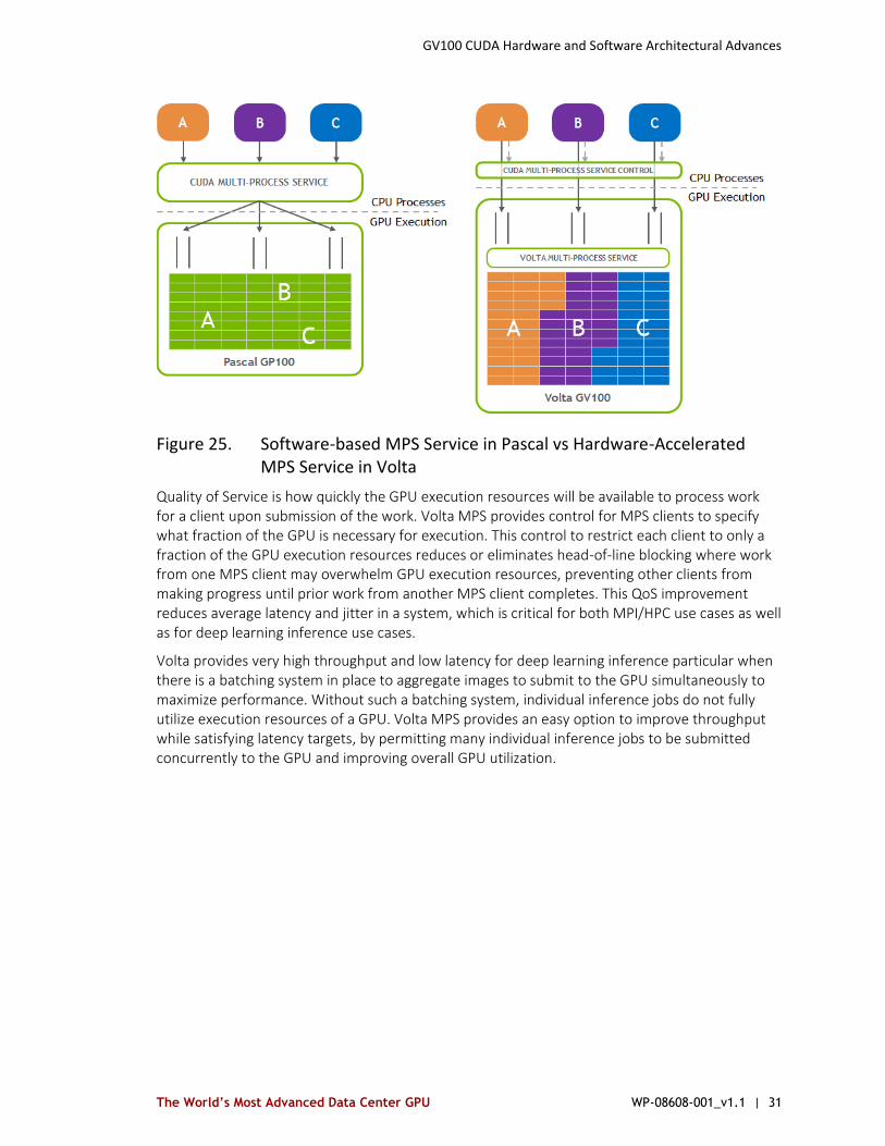
Volta MPS provides hardware acceleration of critical components of the MPS server for improved performance and isolation, while increasing the maximum number of MPS clients from 16 on Pascal up to 48 on Volta (see Figure 25). Volta Multi-Process service is designed for sharing the GPU amongst applications from a single user and is not for multi-user or multi-tenant use cases.
For Pascal, CUDA Multi-Process Service is a CPU process which acts on behalf of GPU applications that have requested to simultaneously share execution resources with other GPU applications. This process acts as the intermediary to submit work to the work queues inside the GPU for concurrent kernel execution.
The Volta Multi-Process Service provides hardware acceleration of CUDA MPS which enables MPS clients to submit work directly to the work queues within the GPU. This acceleration significantly decreases submission latency and increases aggregate throughput. For Volta, the CPU MPS control process remains for configuration and opt-in to the MPS.
Volta MPS improves isolation amongst MPS clients on two critical metrics: Quality of Service (QoS) and independent address spaces. In Volta, the work from different MPS clients A, B, and C get address isolation as shown in Figure 25, in addition to QoS. Volta MPS, as with CUDA MPS on prior NVIDIA GPUs, does not provide fatal fault isolation between clients.
GV100 CUDA Hardware and Software Architectural Advances
The World’s Most Advanced Data Center GPU WP-08608-001_v1.1 | 31
Figure 25. Software-based MPS Service in Pascal vs Hardware-Accelerated MPS Service in Volta
Quality of Service is how quickly the GPU execution resources will be available to process work for a client upon submission of the work. Volta MPS provides control for MPS clients to specify what fraction of the GPU is necessary for execution. This control to restrict each client to only a fraction of the GPU execution resources reduces or eliminates head-of-line blocking where work from one MPS client may overwhelm GPU execution resources, preventing other clients from making progress until prior work from another MPS client completes. This QoS improvement reduces average latency and jitter in a system, which is critical for both MPI/HPC use cases as well as for deep learning inference use cases.
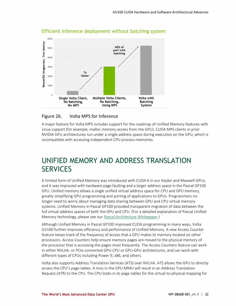
Volta provides very high throughput and low latency for deep learning inference particular when there is a batching system in place to aggregate images to submit to the GPU simultaneously to maximize performance. Without such a batching system, individual inference jobs do not fully utilize execution resources of a GPU. Volta MPS provides an easy option to improve throughput while satisfying latency targets, by permitting many individual inference jobs to be submitted concurrently to the GPU and improving overall GPU utilization.
GV100 CUDA Hardware and Software Architectural Advances
The World’s Most Advanced Data Center GPU WP-08608-001_v1.1 | 32
Figure 26. Volta MPS for Inference
A major feature for Volta MPS includes support for the roadmap of Unified Memory features with Linux support (for example, malloc memory access from the GPU). CUDA MPS clients in prior NVIDIA GPU architectures run under a single address space during execution on the GPU, which is incompatible with accessing independent CPU process memories.
UNIFIED MEMORY AND ADDRESS TRANSLATION SERVICES
A limited form of Unified Memory was introduced with CUDA 6 in our Kepler and Maxwell GPUs, and it was improved with hardware page faulting and a larger address space in the Pascal GP100 GPU. Unified memory allows a single unified virtual address space for CPU and GPU memory, greatly simplifying GPU programming and porting of applications to GPUs. Programmers no longer need to worry about managing data sharing between GPU and CPU virtual memory systems. Unified Memory in Pascal GP100 provided transparent migration of data between the full virtual address spaces of both the GPU and CPU. (For a detailed explanation of Pascal Unified Memory technology, please see our Pascal Architecture Whitepaper.)
Although Unified Memory in Pascal GP100 improved CUDA programming in many ways, Volta GV100 further improves efficiency and performance of Unified Memory. A new Access Counter feature keeps track of the frequency of access that a GPU makes to memory located on other processors. Access Counters help ensure memory pages are moved to the physical memory of the processor that is accessing the pages most frequently. The Access Counters feature can work in either NVLink- or PCIe-connected GPU-CPU or GPU-GPU architectures, and can work with different types of CPUs including Power 9, x86, and others.
Volta also supports Address Translation Services (ATS) over NVLink. ATS allows the GPU to directly access the CPU’s page tables. A miss in the GPU MMU will result in an Address Translation Request (ATR) to the CPU. The CPU looks in its page tables for the virtual-to-physical mapping for
GV100 CUDA Hardware and Software Architectural Advances
The World’s Most Advanced Data Center GPU WP-08608-001_v1.1 | 33
that address and supplies the translation back to the GPU. ATS provides the GPU full access to CPU memory, for example to memory allocated directly with ‘malloc’.
COOPERATIVE GROUPS
In parallel algorithms, threads often need to cooperate to perform collective computations. Building these cooperative codes requires grouping and synchronizing the cooperating threads. CUDA 9 introduces Cooperative Groups, a new programming model for organizing groups of threads.
Historically, the CUDA programming model has provided a single, simple construct for synchronizing cooperating threads: a barrier across all threads of a thread block, as implemented with the __syncthreads( ) function. However, programmers would often like to define groups of threads at smaller than thread block granularities and synchronize within them to enable greater performance, design flexibility, and software reuse in the form of “collective” group-wide function interfaces.
Cooperative Groups introduces the ability to define groups of threads explicitly at sub-block and multiblock granularities, and to perform collective operations such as synchronization on them. This programming model supports clean composition across software boundaries, so that libraries and utility functions can synchronize safely within their local context without having to make assumptions about convergence. It lets developers optimize for the hardware fast path—for example the GPU warp size—using flexible synchronization in a safe, supportable way that makes programmer intent explicit. Cooperative Groups primitives enable new patterns of cooperative parallelism within CUDA, including producer-consumer parallelism, opportunistic parallelism, and global synchronization across the entire grid.
Cooperative Groups also provides an abstraction by which developers can write flexible, scalable code that will work safely across different GPU architectures, including scaling to future GPU capabilities. Thread groups may range in size from a few threads (smaller than a warp) to a whole thread block, to all thread blocks in a grid launch, to grids spanning multiple GPUs.
While Cooperative Groups works on all GPU architectures, certain functionality is inevitably architecture-dependent as GPU capabilities have evolved. Basic functionality, such as synchronizing groups smaller than a thread block down to warp granularity, is supported on all architectures, while Pascal and Volta GPUs enable new grid-wide and multi-GPU synchronizing groups. In addition, Volta’s independent thread scheduling enables significantly more flexible selection and partitioning of thread groups at arbitrary cross-warp and sub-warp granularities. Volta synchronization is truly per thread: threads in a warp can synchronize from divergent code paths.
GV100 CUDA Hardware and Software Architectural Advances
The World’s Most Advanced Data Center GPU WP-08608-001_v1.1 | 34
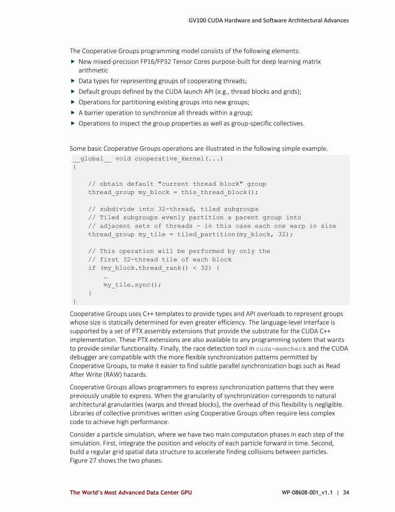
The Cooperative Groups programming model consists of the following elements:
New mixed-precision FP16/FP32 Tensor Cores purpose-built for deep learning matrix arithmetic
Data types for representing groups of cooperating threads;
Default groups defined by the CUDA launch API (e.g., thread blocks and grids);
Operations for partitioning existing groups into new groups;
A barrier operation to synchronize all threads within a group;
Operations to inspect the group properties as well as group-specific collectives.
Some basic Cooperative Groups operations are illustrated in the following simple example.
__global__ void cooperative_kernel(...)
{
// obtain default "current thread block" group
thread_group my_block = this_thread_block();
// subdivide into 32-thread, tiled subgroups
// Tiled subgroups evenly partition a parent group into
// adjacent sets of threads - in this case each one warp in size
thread_group my_tile = tiled_partition(my_block, 32);
// This operation will be performed by only the
// first 32-thread tile of each block
if (my_block.thread_rank() < 32) {
…
my_tile.sync();
}
}
Cooperative Groups uses C++ templates to provide types and API overloads to represent groups whose size is statically determined for even greater efficiency. The language-level interface is supported by a set of PTX assembly extensions that provide the substrate for the CUDA C++ implementation. These PTX extensions are also available to any programming system that wants to provide similar functionality. Finally, the race detection tool in cuda-memcheck and the CUDA debugger are compatible with the more flexible synchronization patterns permitted by Cooperative Groups, to make it easier to find subtle parallel synchronization bugs such as Read After Write (RAW) hazards.
Cooperative Groups allows programmers to express synchronization patterns that they were previously unable to express. When the granularity of synchronization corresponds to natural architectural granularities (warps and thread blocks), the overhead of this flexibility is negligible. Libraries of collective primitives written using Cooperative Groups often require less complex code to achieve high performance.
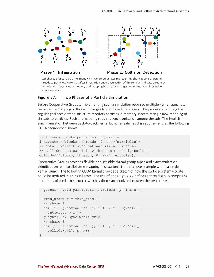
Consider a particle simulation, where we have two main computation phases in each step of the simulation. First, integrate the position and velocity of each particle forward in time. Second, build a regular grid spatial data structure to accelerate finding collisions between particles. Figure 27 shows the two phases.
GV100 CUDA Hardware and Software Architectural Advances
The World’s Most Advanced Data Center GPU WP-08608-001_v1.1 | 35
Figure 27. Two Phases of a Particle Simulation
Before Cooperative Groups, implementing such a simulation required multiple kernel launches, because the mapping of threads changes from phase 1 to phase 2. The process of building the regular grid acceleration structure reorders particles in memory, necessitating a new mapping of threads to particles. Such a remapping requires synchronization among threads. The implicit synchronization between back-to-back kernel launches satisfies this requirement, as the following CUDA pseudocode shows.
// threads update particles in parallel
integrate<<<blocks, threads, 0, s>>>(particles);
// Note: implicit sync between kernel launches
// Collide each particle with others in neighborhood
collide<<<blocks, threads, 0, s>>>(particles);
Cooperative Groups provides flexible and scalable thread group types and synchronization primitives enable parallelism remapping in situations like the above example within a single kernel launch. The following CUDA kernel provides a sketch of how the particle system update could be updated in a single kernel. The use of this_grid() defines a thread group comprising all threads of the kernel launch, which is then synchronized between the two phases.
__global__ void particleSim(Particle *p, int N) {
grid_group g = this_grid();
// phase 1
for (i = g.thread_rank(); i < N; i += g.size())
integrate(p[i]);
g.sync() // Sync whole grid
// phase 2
for (i = g.thread_rank(); i < N; i += g.size())
collide(p[i], p, N);
}
Two phases of a particle simulation, with numbered arrows representing the mapping of parallel threads to particles. Note that after integration and construction of the regular grid data structure, the ordering of particles in memory and mapping to threads changes, requiring a synchronization between phases
GV100 CUDA Hardware and Software Architectural Advances
The World’s Most Advanced Data Center GPU WP-08608-001_v1.1 | 36
This kernel is written in such a way that it is trivial to extend the simulation to multiple GPUs. The Cooperative Groups function this_multi_grid() returns a thread group spanning all threads of a kernel launch across multiple GPUs. Calling sync() on this group synchronizes all threads running the kernel on multiple GPUs. Note that in both cases, the thread_rank() method provides a linear index of the current thread within the thread group, which the kernel uses to iterate over the particles in parallel in case there are more particles than threads.
__global__ void particleSim(Particle *p, int N) {
multi_grid_group g = this_multi_grid();
// phase 1
for (i = g.thread_rank(); i < N; i += g.size())
integrate(p[i]);
g.sync() // Sync whole grid
// phase 2
for (i = g.thread_rank(); i < N; i += g.size())
collide(p[i], p, N);
}
To use groups that span multiple thread blocks or multiple GPUs, applications must use the cudaLaunchCooperativeKernel() or cudaLaunchCooperativeKernelMultiDevice() API, respectively. Synchronization requires that all thread blocks are simultaneously resident, so the application must also ensure that the resource usage (registers and shared memory) of the thread blocks launched does not exceed the total resources of the GPU(s).
CONCLUSION
The NVIDIA Tesla V100 accelerator based on the new Volta GV100 GPU is the world’s most advanced data center GPU ever built. V100 can accelerate AI, HPC, and Graphics, enabling data scientists, researchers, and engineers to tackle challenges that were once thought impossible.
Volta is the most powerful GPU architecture the world has ever seen, and GV100 is the first processor to break the 100 TFLOPS barrier of deep learning performance. GV100 couples CUDA cores and Tensor Cores to deliver the performance of an AI supercomputer in a GPU. The second generation of NVIDIA NVLink connects multiple V100 GPUs at up to 300 GB/s to create the world’s most powerful computing servers. AI models that consumed weeks of computing resources in the past can now be trained in a few days with Tesla V100-accelerated systems. With such a dramatic reduction in training time, a whole new world of problems will now be solvable with AI powered by the NVIDIA Tesla V100 accelerator.
The World’s Most Advanced Data Center GPU WP-08608-001_v1.1 | 37
APPENDIX A NVIDIA DGX-1 WITH TESLA V100
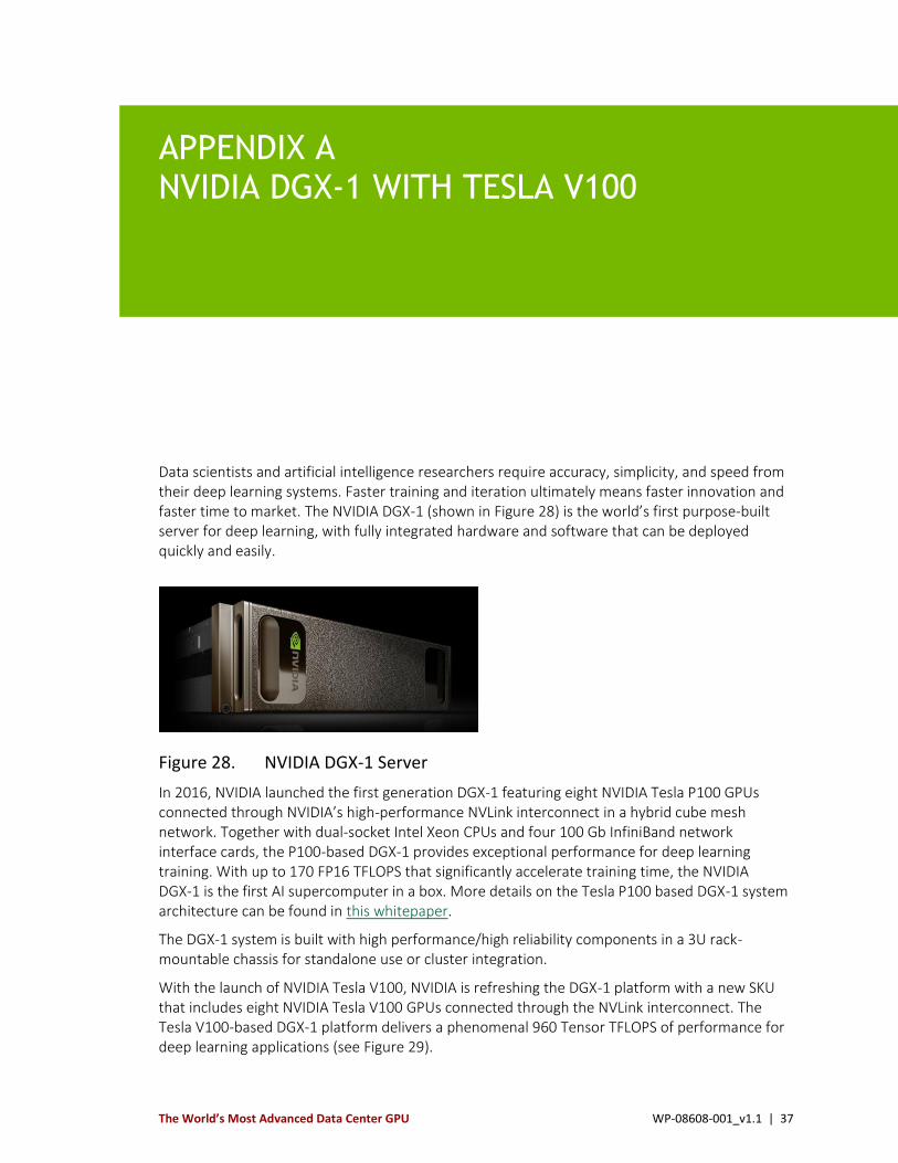
Data scientists and artificial intelligence researchers require accuracy, simplicity, and speed from their deep learning systems. Faster training and iteration ultimately means faster innovation and faster time to market. The NVIDIA DGX-1 (shown in Figure 28) is the world’s first purpose-built server for deep learning, with fully integrated hardware and software that can be deployed quickly and easily.
Figure 28. NVIDIA DGX-1 Server
In 2016, NVIDIA launched the first generation DGX-1 featuring eight NVIDIA Tesla P100 GPUs connected through NVIDIA’s high-performance NVLink interconnect in a hybrid cube mesh network. Together with dual-socket Intel Xeon CPUs and four 100 Gb InfiniBand network interface cards, the P100-based DGX-1 provides exceptional performance for deep learning training. With up to 170 FP16 TFLOPS that significantly accelerate training time, the NVIDIA DGX-1 is the first AI supercomputer in a box. More details on the Tesla P100 based DGX-1 system architecture can be found in this whitepaper.
The DGX-1 system is built with high performance/high reliability components in a 3U rack-mountable chassis for standalone use or cluster integration.
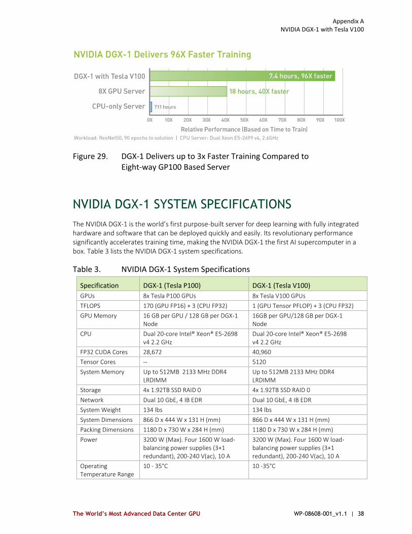
With the launch of NVIDIA Tesla V100, NVIDIA is refreshing the DGX-1 platform with a new SKU that includes eight NVIDIA Tesla V100 GPUs connected through the NVLink interconnect. The Tesla V100-based DGX-1 platform delivers a phenomenal 960 Tensor TFLOPS of performance for deep learning applications (see Figure 29).
Appendix A NVIDIA DGX-1 with Tesla V100
The World’s Most Advanced Data Center GPU WP-08608-001_v1.1 | 38
Figure 29. DGX-1 Delivers up to 3x Faster Training Compared to Eight-way GP100 Based Server
NVIDIA DGX-1 SYSTEM SPECIFICATIONS
The NVIDIA DGX-1 is the world’s first purpose-built server for deep learning with fully integrated hardware and software that can be deployed quickly and easily. Its revolutionary performance significantly accelerates training time, making the NVIDIA DGX-1 the first AI supercomputer in a box. Table 3 lists the NVIDIA DGX-1 system specifications.
Table 3. NVIDIA DGX-1 System Specifications
Specification DGX-1 (Tesla P100) DGX-1 (Tesla V100)
GPUs 8x Tesla P100 GPUs 8x Tesla V100 GPUs
TFLOPS 170 (GPU FP16) + 3 (CPU FP32) 1 (GPU Tensor PFLOP) + 3 (CPU FP32)
GPU Memory 16 GB per GPU / 128 GB per DGX-1 Node
16GB per GPU/128 GB per DGX-1 Node
CPU Dual 20-core Intel® Xeon® E5-2698 v4 2.2 GHz
Dual 20-core Intel® Xeon® E5-2698 v4 2.2 GHz
FP32 CUDA Cores 28,672 40,960
Tensor Cores -- 5120
System Memory Up to 512MB 2133 MHz DDR4 LRDIMM
Up to 512MB 2133 MHz DDR4 LRDIMM
Storage 4x 1.92TB SSD RAID 0 4x 1.92TB SSD RAID 0
Network Dual 10 GbE, 4 IB EDR Dual 10 GbE, 4 IB EDR
System Weight 134 lbs 134 lbs
System Dimensions 866 D x 444 W x 131 H (mm) 866 D x 444 W x 131 H (mm)
Packing Dimensions 1180 D x 730 W x 284 H (mm) 1180 D x 730 W x 284 H (mm)
Power 3200 W (Max). Four 1600 W load-balancing power supplies (3+1 redundant), 200-240 V(ac), 10 A
3200 W (Max). Four 1600 W load-balancing power supplies (3+1 redundant), 200-240 V(ac), 10 A
Operating Temperature Range
10 - 35°C 10 -35°C
Appendix A NVIDIA DGX-1 with Tesla V100
The World’s Most Advanced Data Center GPU WP-08608-001_v1.1 | 39
DGX-1 SOFTWARE Along with the powerful DGX-1 hardware, a comprehensive, integrated software stack of development tools and libraries is included and optimized to run deep learning at scale. A key goal is to enable practitioners to deploy deep learning frameworks and applications on DGX-1 with minimal setup effort.
The design of the platform software is centered around a minimal OS and driver install on the server. Provisioning of all application and SDK software is enabled with containers called NVIDIA Docker, through the DGX Container Registry2 maintained by NVIDIA.
Containers available for DGX-1 include multiple optimized deep learning frameworks, the NVIDIA DIGITS deep learning training application, third party accelerated solutions, and the NVIDIA CUDA Toolkit.
This software architecture has many advantages:
Since each deep learning framework is in a separate container, each framework can use different versions of libraries like libc, cuDNN, and others, and not interfere with each other.
As deep learning frameworks are improved for performance or bug fixes, new versions of containers are made available in the DGX Container Registry.
The system is easy to maintain, and the OS image stays clean, since applications are not installed directly on the OS.
Security updates, driver updates, and OS patches can be delivered seamlessly.
The deep learning frameworks and the CUDA Toolkit include libraries that have been custom-tuned to provide high multi-GPU performance on DGX-1. Figure 30 shows the DGX-1 deep learning stack.
2 Docker registry service provided by NVIDIA. See http://docs.nvidia.com/dgx/dgx-registry-guide/
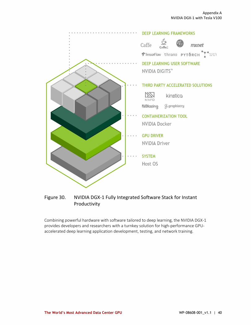
Appendix A NVIDIA DGX-1 with Tesla V100
The World’s Most Advanced Data Center GPU WP-08608-001_v1.1 | 40
Figure 30. NVIDIA DGX-1 Fully Integrated Software Stack for Instant Productivity
Combining powerful hardware with software tailored to deep learning, the NVIDIA DGX-1 provides developers and researchers with a turnkey solution for high-performance GPU-accelerated deep learning application development, testing, and network training.
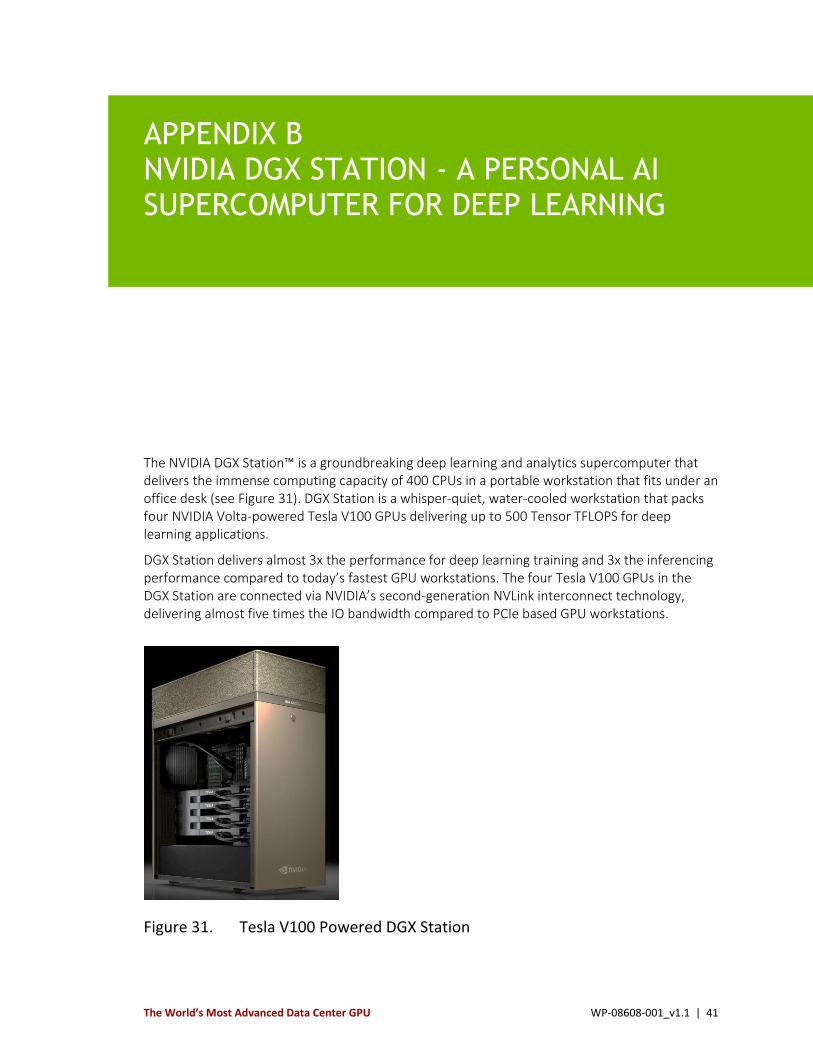
The World’s Most Advanced Data Center GPU WP-08608-001_v1.1 | 41
APPENDIX B NVIDIA DGX STATION - A PERSONAL AI SUPERCOMPUTER FOR DEEP LEARNING
The NVIDIA DGX Station™ is a groundbreaking deep learning and analytics supercomputer that delivers the immense computing capacity of 400 CPUs in a portable workstation that fits under an office desk (see Figure 31). DGX Station is a whisper-quiet, water-cooled workstation that packs four NVIDIA Volta-powered Tesla V100 GPUs delivering up to 500 Tensor TFLOPS for deep learning applications.
DGX Station delivers almost 3x the performance for deep learning training and 3x the inferencing performance compared to today’s fastest GPU workstations. The four Tesla V100 GPUs in the DGX Station are connected via NVIDIA’s second-generation NVLink interconnect technology, delivering almost five times the IO bandwidth compared to PCIe based GPU workstations.
Figure 31. Tesla V100 Powered DGX Station

Appendix B NVIDIA DGX Station - A Personal AI Supercomputer for Deep Learning
The World’s Most Advanced Data Center GPU WP-08608-001_v1.1 | 42
Figure 32 shows the DGX Station performance when powered by a four-way Tesla V100. The Tesla V100 is 47x faster than CPU-based server3 performance. Table 4 lists the DGX Station specifications.
Figure 32. NVIDIA DGX Station Delivers 47x Faster Training
Table 4. DGX Station Specifications
Specification DGX Station
GPUs 4 NVIDIA Tesla V100 interconnected via NVLink
TFLOPS 500 Tensor TFLOPS, 15.7 FP32 TFLOPS
Tensor Cores 2560
CPU Intel Xeon E5-2698 v4 2.2 GHz (20-core)
System Memory 256 GB LRDIMM DDR4
Storage Data: 3 x 1.92 TB SSD RAID 0
OS: 1 x 1.92 TB SSD
Network Dual 10 Gb LAN
Display 3x DisplayPort
Acoustics < 35 dB
System Weight 88 lbs / 40 kgs
System Dimensions 518 mm (D) x 256 mm (W) x 639 mm (H)
Maximum Power 1500 Watts
Operation Temperature 10⁰ C - 30⁰ C
Operating System Ubuntu Desktop Linux
3 Workload: ResNet50, 90 epochs to solution | CPU Server: Dual Xeon E5-2699 v4, 2.6GHz
Appendix B NVIDIA DGX Station - A Personal AI Supercomputer for Deep Learning
The World’s Most Advanced Data Center GPU WP-08608-001_v1.1 | 43
PRELOADED WITH THE LATEST DEEP LEARNING SOFTWARE
NVIDIA DGX Station comes preloaded with the same software stack found in all DGX solutions. This innovative, integrated software stack includes access to popular deep learning frameworks, each optimized by NVIDIA deep learning experts and updated monthly. It also comes with NVIDIA DIGITS deep learning training application, third-party accelerated solutions, the NVIDIA deep learning SDKs such as cuDNN and cuBLAS, CUDA toolkit, fast multi-GPU collectives (called NCCL), and NVIDIA drivers.
This comprehensive deep learning software stack is continually tuned, optimized, and delivered through the same NVIDIA Docker containers and NVIDIA Container Registry service that are used for all DGX platforms. This single unified deep learning stack simplifies workflows. Data scientists can now easily scale their work and deploy the solutions developed with DGX Station onto DGX-1 servers in the data center or the NVIDIA Deep Learning Cloud.
Equally important and noteworthy, with NVIDIA maintaining and delivering the software stack, data scientists can now focus purely on training and deploying their deep learning solutions, and not waste time tuning and updating software components. The thousands of dollars of potential cost savings from improved productivity and better utilization of scarce deep learning expertise dwarfs the initial cost of the hardware.
KICKSTARTING AI INITIATIVES
NVIDIA DGX Station is designed to kickstart the AI initiatives of individual researchers or organizations with a streamlined plug-in and power-up experience that can have them training neural networks in just one day.
DGX Station delivers tremendous compute performance and the peace of mind that comes with an integrated solution that includes:
Enterprise-grade support
Access to NVIDIA deep learning expertise
Tools library and software optimized for deep learning
Timely software upgrades
Priority resolution of critical issues
DGX Station combined with NVIDIA tools and knowledge enables data scientist to deliver their best work.
For more information on NVIDIA DGX Station, visit www.nvidia.com/dgx-station.

The World’s Most Advanced Data Center GPU WP-08608-001_v1.1 | 44
APPENDIX C ACCELERATING DEEP LEARNING AND ARTIFICIAL INTELLIGENCE WITH GPUS
In the past five years, deep neural networks (DNNs) developed on GPUs have conquered one algorithm domain after another. The potential use cases are endless: From self-driving cars to faster drug development, from automatic image captioning in online image databases to smart real-time language translation in video chat applications, deep learning is providing exciting opportunities wherever machines interact with the human world. In this section, we’ll provide a brief introduction to deep learning and how customers are using GPUs to enable the next generation of deep learning breakthroughs.
DEEP LEARNING IN A NUTSHELL
Deep learning is a technique that models the neural learning process of the human brain, continually learning, continually getting smarter, and delivering more accurate results more quickly over time. A child is initially taught by an adult to correctly identify and classify various shapes, eventually being able to identify shapes without any coaching. Similarly, a deep learning or neural learning system needs to be trained in object recognition and classification for it get smarter and more efficient at identifying basic objects, occluded objects, etc., while also assigning context to objects.
At the simplest level, neurons in the human brain look at various inputs fed into them, importance levels are assigned to each of these inputs, and output is passed on to other neurons to act upon.
The Perceptron as shown in Figure 33 is the most basic model of a neural network and is akin to a neuron in the human brain. As seen in the image, the Perceptron has several inputs that represent various features of an object that the Perceptron is being trained to recognize and classify, and each of these features is assigned a certain weight based on the importance of that feature in defining the shape of an object.
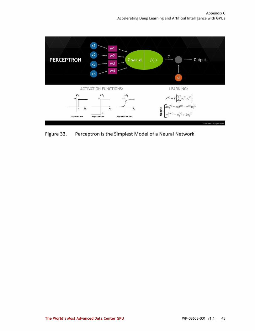
Appendix C Accelerating Deep Learning and Artificial Intelligence with GPUs
The World’s Most Advanced Data Center GPU WP-08608-001_v1.1 | 45
Figure 33. Perceptron is the Simplest Model of a Neural Network

Appendix C Accelerating Deep Learning and Artificial Intelligence with GPUs
The World’s Most Advanced Data Center GPU WP-08608-001_v1.1 | 46
For example, consider a Perceptron that is being trained to identify the number zero that is handwritten. Obviously, the number zero can be written in different ways based on different handwriting styles. The Perceptron will take the image of the number zero, decompose it into various sections and assign these sections to features x1 through x4. The upper right-hand curve in the number zero may be assigned to x1, the lower bottom curve to x2, and so on. The weight associated with a particular feature determines how important that feature is in correctly determining whether the handwritten number is a zero. The green blob at the center of the diagram is where the Perceptron is calculating the weighted sum of all the features in the image to determine whether the number is a zero. A function is then applied on this result to output a true or false value on whether the number is a zero.
The key aspect of a neural network is in training the network to make better predictions. The Perceptron model (shown in Figure 33) to detect handwritten zeros is trained by initially assigning a set of weights to each of the features that define the number zero. The Perceptron is then provided with the number zero to check whether it correctly identifies the number. This flow of data through the network until it reaches a conclusion on whether the number is zero or not, is the forward propagation phase. If the neural network does not correctly identify the number, then the reason for the incorrect identification needs to be understood, along with the magnitude of the error, and the weights need to be adjusted for each feature until the perceptron correctly identifies a zero. The weights need further adjusting until it correctly identifies zeros written in various handwriting styles. This process of feeding back the errors and adjusting the weights of each feature that defines the number zero is called backward propagation. The equations shown in the diagram look complex, but are basically mathematical representations of the described training process.
Though the Perceptron is a very simple model of a neural network, advanced multi-layered neural networks based on similar concepts are widely used today. Once a network has been trained to correctly identify and classify the objects, it is deployed in the field, where it will repeatedly run inference computations. Examples of inference (the process through which a DNN extracts useful information from a given input) include identifying handwritten numbers on checks deposited into ATM machines, identifying images of friends in Facebook photos, delivering movie recommendations to over fifty million Netflix users, identifying and classifying different types of automobiles, pedestrians, and road hazards in driverless cars, or translating human speech in real-time.
A multi-layered neural network model, as shown in Figure 34, consists of multiple interconnected, complex Perceptron-like nodes. Each node looks at many input features, and feeds its output to the next several layers of interconnected nodes.
In the model shown in Figure 34, the first layer of the neural model breaks down the automobile image into various sections, and looks for basic patterns such as lines and angles. The second layer assembles these lines to look for higher level patterns such as wheels, windshields, and mirrors. The next layer identifies the type of vehicle, and the final few layers identify the model of a specific automobile brand (which in this case is an Audi A7).
An alternative to a fully connected layer of a neural network is a convolutional layer. A neuron in a convolutional layer is connected to neurons only in a small region in the layer below it. Typically, this region might be a 5×5 grid of neurons (or perhaps 7×7 or 11×11). The size of this grid is called the filter size. Thus, a convolutional layer can be thought of as performing a convolution on its input. This type of connection pattern mimics the pattern seen in perceptual areas of the brain, such as retinal ganglion cells or cells in the primary visual cortex.
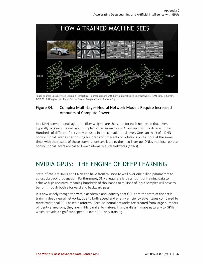
Appendix C Accelerating Deep Learning and Artificial Intelligence with GPUs
The World’s Most Advanced Data Center GPU WP-08608-001_v1.1 | 47
Image source: Unsupervised Learning Hierarchical Representations with Convolutional Deep Brief Networks, ICML 2009 & Comm. ACM 2011, Honglak Lee, Roger Grosse, Rajesh Ranganath, and Andrew Ng.
Figure 34. Complex Multi-Layer Neural Network Models Require Increased Amounts of Compute Power
In a DNN convolutional layer, the filter weights are the same for each neuron in that layer. Typically, a convolutional layer is implemented as many sub layers each with a different filter. Hundreds of different filters may be used in one convolutional layer. One can think of a DNN convolutional layer as performing hundreds of different convolutions on its input at the same time, with the results of these convolutions available to the next layer up. DNNs that incorporate convolutional layers are called Convolutional Neural Networks (CNNs).
NVIDIA GPUS: THE ENGINE OF DEEP LEARNING
State-of-the-art DNNs and CNNs can have from millions to well over one billion parameters to adjust via back-propagation. Furthermore, DNNs require a large amount of training data to achieve high accuracy, meaning hundreds of thousands to millions of input samples will have to be run through both a forward and backward pass.
It is now widely recognized within academia and industry that GPUs are the state of the art in training deep neural networks, due to both speed and energy efficiency advantages compared to more traditional CPU-based platforms. Because neural networks are created from large numbers of identical neurons, they are highly parallel by nature. This parallelism maps naturally to GPUs, which provide a significant speedup over CPU-only training.
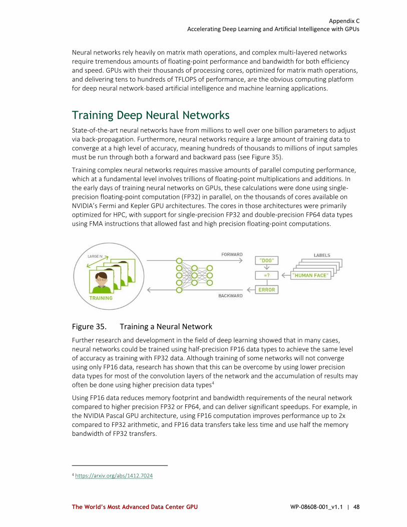
Appendix C Accelerating Deep Learning and Artificial Intelligence with GPUs
The World’s Most Advanced Data Center GPU WP-08608-001_v1.1 | 48
Neural networks rely heavily on matrix math operations, and complex multi-layered networks require tremendous amounts of floating-point performance and bandwidth for both efficiency and speed. GPUs with their thousands of processing cores, optimized for matrix math operations, and delivering tens to hundreds of TFLOPS of performance, are the obvious computing platform for deep neural network-based artificial intelligence and machine learning applications.
Training Deep Neural Networks
State-of-the-art neural networks have from millions to well over one billion parameters to adjust via back-propagation. Furthermore, neural networks require a large amount of training data to converge at a high level of accuracy, meaning hundreds of thousands to millions of input samples must be run through both a forward and backward pass (see Figure 35).
Training complex neural networks requires massive amounts of parallel computing performance, which at a fundamental level involves trillions of floating-point multiplications and additions. In the early days of training neural networks on GPUs, these calculations were done using single-precision floating-point computation (FP32) in parallel, on the thousands of cores available on NVIDIA’s Fermi and Kepler GPU architectures. The cores in those architectures were primarily optimized for HPC, with support for single-precision FP32 and double-precision FP64 data types using FMA instructions that allowed fast and high precision floating-point computations.
Figure 35. Training a Neural Network
Further research and development in the field of deep learning showed that in many cases, neural networks could be trained using half-precision FP16 data types to achieve the same level of accuracy as training with FP32 data. Although training of some networks will not converge using only FP16 data, research has shown that this can be overcome by using lower precision data types for most of the convolution layers of the network and the accumulation of results may often be done using higher precision data types4
Using FP16 data reduces memory footprint and bandwidth requirements of the neural network compared to higher precision FP32 or FP64, and can deliver significant speedups. For example, in the NVIDIA Pascal GPU architecture, using FP16 computation improves performance up to 2x compared to FP32 arithmetic, and FP16 data transfers take less time and use half the memory bandwidth of FP32 transfers.
4 https://arxiv.org/abs/1412.7024
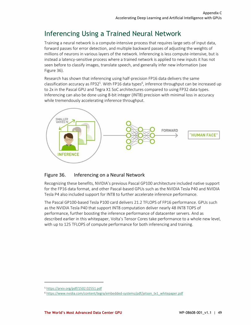
Appendix C Accelerating Deep Learning and Artificial Intelligence with GPUs
The World’s Most Advanced Data Center GPU WP-08608-001_v1.1 | 49
Inferencing Using a Trained Neural Network
Training a neural network is a compute-intensive process that requires large sets of input data, forward passes for error detection, and multiple backward passes of adjusting the weights of millions of neurons in various layers of the network. Inferencing is less compute-intensive, but is instead a latency-sensitive process where a trained network is applied to new inputs it has not seen before to classify images, translate speech, and generally infer new information (see Figure 36).
Research has shown that inferencing using half-precision FP16 data delivers the same classification accuracy as FP325. With FP16 data types6, inference throughput can be increased up to 2x in the Pascal GPU and Tegra X1 SoC architectures compared to using FP32 data types. Inferencing can also be done using 8-bit integer (INT8) precision with minimal loss in accuracy while tremendously accelerating inference throughput.
Figure 36. Inferencing on a Neural Network
Recognizing these benefits, NVIDIA’s previous Pascal GP100 architecture included native support for the FP16 data format, and other Pascal-based GPUs such as the NVIDIA Tesla P40 and NVIDIA Tesla P4 also included support for INT8 to further accelerate inference performance.
The Pascal GP100-based Tesla P100 card delivers 21.2 TFLOPS of FP16 performance. GPUs such as the NVIDIA Tesla P40 that support INT8 computation deliver nearly 48 INT8 TOPS of performance, further boosting the inference performance of datacenter servers. And as described earlier in this whitepaper, Volta’s Tensor Cores take performance to a whole new level, with up to 125 TFLOPS of compute performance for both inferencing and training.
5 https://arxiv.org/pdf/1502.02551.pdf 6 https://www.nvidia.com/content/tegra/embedded-systems/pdf/jetson_tx1_whitepaper.pdf

Appendix C Accelerating Deep Learning and Artificial Intelligence with GPUs
The World’s Most Advanced Data Center GPU WP-08608-001_v1.1 | 50
COMPREHENSIVE DEEP LEARNING SOFTWARE DEVELOPMENT KIT
AI innovation is on a breakneck pace. Ease of programming and developer productivity is paramount. The programmability and richness of NVIDIA’s CUDA platform allow researchers to innovate quickly. NVIDIA provides high-performance tools and libraries such as NVIDIA DIGITS™, cuDNN, cuBLAS and others to power innovative GPU-accelerated machine learning applications in the cloud, data centers, workstations, and embedded platforms with the deep learning Software Development Kit (SDK).
Developers want to create anywhere and deploy everywhere. NVIDIA GPUs are available all over the world, from every PC OEM; in desktops, notebooks, servers, or supercomputers; and in the cloud from major companies like Amazon, Google, IBM, Facebook, Baidu and Microsoft. All major AI development frameworks are NVIDIA GPU accelerated—from Internet companies, to research, to startups. No matter the AI development system preferred, it will be faster with GPU acceleration.
NVIDIA has also created GPUs for just about every computing form-factor so that DNNs can power intelligent machines of all kinds. GeForce is for PC. Tesla is for cloud and supercomputers. Jetson is for robots and drones. And DRIVE PX 2 is for cars. All share the same architecture and accelerate deep learning (see Figure 37).
Figure 37. Accelerate Every Framework
Baidu, Google, Facebook, Microsoft were among the earliest adopters of NVIDIA GPUs for deep learning and AI processing. In fact, AI technology enables these companies to respond to your spoken word, translate speech or text to another language, recognize and automatically tag images, and recommend newsfeeds, entertainment, and products that are tailored to each user.
Startups and established companies are now racing to use AI to create new products and services, or improve their operations. In just two years, the number of companies NVIDIA collaborates with on deep learning has jumped nearly 13x to over 19000 companies (see Figure 38).

Appendix C Accelerating Deep Learning and Artificial Intelligence with GPUs
The World’s Most Advanced Data Center GPU WP-08608-001_v1.1 | 51
Industries such as healthcare, life sciences, energy, financial services, automotive, manufacturing, and entertainment will benefit by inferring insight from mountains of data. And with Facebook, Google, and Microsoft opening their deep-learning platforms for all to use, AI-powered applications will spread fast.
Figure 38. Organizations Engaged with NVIDIA on Deep Learning
Self-driving Cars
Whether to augment humans with a superhuman co-pilot, or revolutionize personal mobility services, or reduce the need for sprawling parking lots within cities, self-driving cars have the potential to do amazing social good. Driving is complicated. Unexpected things happen. Freezing rain turns the road into a skating rink. The road to your destination is closed. A child runs out in front of the car. You can’t write software that anticipates every possible scenario a self-driving car might encounter. That’s the value of deep learning; it can learn, adapt, and improve. NVIDIA is building end-to-end deep learning platform solutions for self-driving cars with NVIDIA DRIVE PX 2, NVIDIA DriveWorks, and NVIDIA DriveNet (see Figure 39)— from the training system to the in-car AI computer. The results are very exciting. A future with superhuman computer co-pilots and driverless shuttles is no longer science fiction.
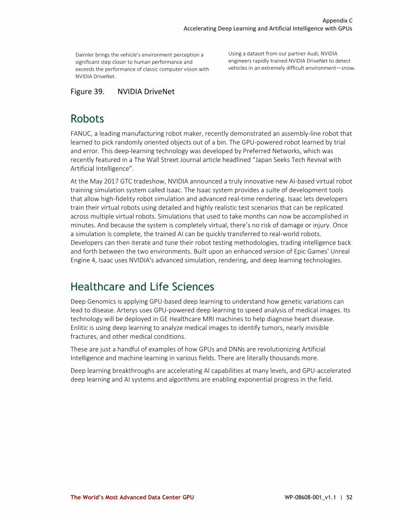
Appendix C Accelerating Deep Learning and Artificial Intelligence with GPUs
The World’s Most Advanced Data Center GPU WP-08608-001_v1.1 | 52
Figure 39. NVIDIA DriveNet
Robots
FANUC, a leading manufacturing robot maker, recently demonstrated an assembly-line robot that learned to pick randomly oriented objects out of a bin. The GPU-powered robot learned by trial and error. This deep-learning technology was developed by Preferred Networks, which was recently featured in a The Wall Street Journal article headlined “Japan Seeks Tech Revival with Artificial Intelligence”.
At the May 2017 GTC tradeshow, NVIDIA announced a truly innovative new AI-based virtual robot training simulation system called Isaac. The Isaac system provides a suite of development tools that allow high-fidelity robot simulation and advanced real-time rendering. Isaac lets developers train their virtual robots using detailed and highly realistic test scenarios that can be replicated across multiple virtual robots. Simulations that used to take months can now be accomplished in minutes. And because the system is completely virtual, there’s no risk of damage or injury. Once a simulation is complete, the trained AI can be quickly transferred to real-world robots. Developers can then iterate and tune their robot testing methodologies, trading intelligence back and forth between the two environments. Built upon an enhanced version of Epic Games' Unreal Engine 4, Isaac uses NVIDIA's advanced simulation, rendering, and deep learning technologies.
Healthcare and Life Sciences
Deep Genomics is applying GPU-based deep learning to understand how genetic variations can lead to disease. Arterys uses GPU-powered deep learning to speed analysis of medical images. Its technology will be deployed in GE Healthcare MRI machines to help diagnose heart disease. Enlitic is using deep learning to analyze medical images to identify tumors, nearly invisible fractures, and other medical conditions.
These are just a handful of examples of how GPUs and DNNs are revolutionizing Artificial Intelligence and machine learning in various fields. There are literally thousands more.
Deep learning breakthroughs are accelerating AI capabilities at many levels, and GPU-accelerated deep learning and AI systems and algorithms are enabling exponential progress in the field.
Daimler brings the vehicle’s environment perception a significant step closer to human performance and exceeds the performance of classic computer vision with NVIDIA DriveNet.
Using a dataset from our partner Audi, NVIDIA engineers rapidly trained NVIDIA DriveNet to detect vehicles in an extremely difficult environment—snow.

www.nvidia.com
Notice The information provided in this specification is believed to be accurate and reliable as of the date provided. However, NVIDIA Corporation (“NVIDIA”) does not give any representations or warranties, expressed or implied, as to the accuracy or completeness of such information. NVIDIA shall have no liability for the consequences or use of such information or for any infringement of patents or other rights of third parties that may result from its use. This publication supersedes and replaces all other specifications for the product that may have been previously supplied. NVIDIA reserves the right to make corrections, modifications, enhancements, improvements, and other changes to this specification, at any time and/or to discontinue any product or service without notice. Customer should obtain the latest relevant specification before placing orders and should verify that such information is current and complete. NVIDIA products are sold subject to the NVIDIA standard terms and conditions of sale supplied at the time of order acknowledgement, unless otherwise agreed in an individual sales agreement signed by authorized representatives of NVIDIA and customer. NVIDIA hereby expressly objects to applying any customer general terms and conditions with regard to the purchase of the NVIDIA product referenced in this specification. NVIDIA products are not designed, authorized or warranted to be suitable for use in medical, military, aircraft, space or life support equipment, nor in applications where failure or malfunction of the NVIDIA product can reasonably be expected to result in personal injury, death or property or environmental damage. NVIDIA accepts no liability for inclusion and/or use of NVIDIA products in such equipment or applications and therefore such inclusion and/or use is at customer’s own risk. NVIDIA makes no representation or warranty that products based on these specifications will be suitable for any specified use without further testing or modification. Testing of all parameters of each product is not necessarily performed by NVIDIA. It is customer’s sole responsibility to ensure the product is suitable and fit for the application planned by customer and to do the necessary testing for the application in order to avoid a default of the application or the product. Weaknesses in customer’s product designs may affect the quality and reliability of the NVIDIA product and may result in additional or different conditions and/or requirements beyond those contained in this specification. NVIDIA does not accept any liability related to any default, damage, costs or problem which may be based on or attributable to: (i) the use of the NVIDIA product in any manner that is contrary to this specification, or (ii) customer product designs. No license, either expressed or implied, is granted under any NVIDIA patent right, copyright, or other NVIDIA intellectual property right under this specification. Information published by NVIDIA regarding third-party products or services does not constitute a license from NVIDIA to use such products or services or a warranty or endorsement thereof. Use of such information may require a license from a third party under the patents or other intellectual property rights of the third party, or a license from NVIDIA under the patents or other intellectual property rights of NVIDIA. Reproduction of information in this specification is permissible only if reproduction is approved by NVIDIA in writing, is reproduced without alteration, and is accompanied by all associated conditions, limitations, and notices. ALL NVIDIA DESIGN SPECIFICATIONS, REFERENCE BOARDS, FILES, DRAWINGS, DIAGNOSTICS, LISTS, AND OTHER DOCUMENTS (TOGETHER AND SEPARATELY, “MATERIALS”) ARE BEING PROVIDED “AS IS.” NVIDIA MAKES NO WARRANTIES, EXPRESSED, IMPLIED, STATUTORY, OR OTHERWISE WITH RESPECT TO THE MATERIALS, AND EXPRESSLY DISCLAIMS ALL IMPLIED WARRANTIES OF NONINFRINGEMENT, MERCHANTABILITY, AND FITNESS FOR A PARTICULAR PURPOSE. Notwithstanding any damages that customer might incur for any reason whatsoever, NVIDIA’s aggregate and cumulative liability towards customer for the products described herein shall be limited in accordance with the NVIDIA terms and conditions of sale for the product.
VESA DisplayPort DisplayPort and DisplayPort Compliance Logo, DisplayPort Compliance Logo for Dual-mode Sources, and DisplayPort Compliance Logo for Active Cables are trademarks owned by the Video Electronics Standards Association in the United States and other countries.
HDMI HDMI, the HDMI logo, and High-Definition Multimedia Interface are trademarks or registered trademarks of HDMI Licensing LLC.
ARM ARM, AMBA and ARM Powered are registered trademarks of ARM Limited. Cortex, MPCore and Mali are trademarks of ARM Limited. All other brands or product names are the property of their respective holders. ʺARMʺ is used to represent ARM Holdings plc; its operating company ARM Limited; and the regional subsidiaries ARM Inc.; ARM KK; ARM Korea Limited.; ARM Taiwan Limited; ARM France SAS; ARM Consulting (Shanghai) Co. Ltd.; ARM Germany GmbH; ARM Embedded Technologies Pvt. Ltd.; ARM Norway, AS and ARM Sweden AB.
OpenCL OpenCL is a trademark of Apple Inc. used under license to the Khronos Group Inc.
Trademarks NVIDIA, the NVIDIA logo, TESLA, NVIDIA DGX Station, NVLink, and CUDA are trademarks and/or registered trademarks of NVIDIA Corporation in the U.S. and other countries. Other company and product names may be trademarks of the respective companies with which they are associated.
Copyright © 2017 NVIDIA Corporation. All rights reserved.