observation of nanoscale refractive index contrast via photoinduced ... · observation of nanoscale...
TRANSCRIPT
Observation of Nanoscale Refractive Index Contrast viaPhotoinduced Force MicroscopyAntonio Ambrosio,*,†,‡,§ Robert Charles Devlin,∥ Federico Capasso,∥ and William L. Wilson*,†
†Center for Nanoscale Systems, ‡Department of Physics, and ∥Harvard John A. Paulson School of Engineering and Applied Sciences,Harvard University, Cambridge, Massachusetts 02138, United States§CNR-SPIN U.O.S. Napoli, Complesso Universitario di Monte Sant’Angelo, Via Cintia, 80126 − Napoli, Italy
*S Supporting Information
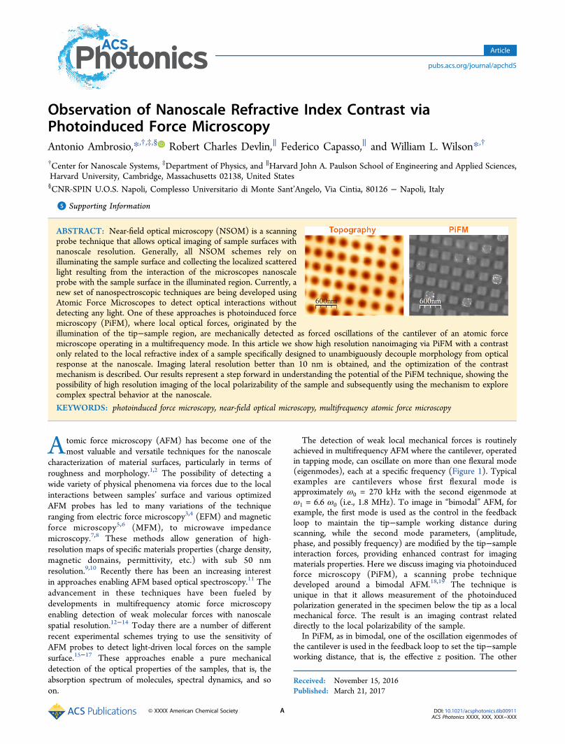
ABSTRACT: Near-field optical microscopy (NSOM) is a scanningprobe technique that allows optical imaging of sample surfaces withnanoscale resolution. Generally, all NSOM schemes rely onilluminating the sample surface and collecting the localized scatteredlight resulting from the interaction of the microscopes nanoscaleprobe with the sample surface in the illuminated region. Currently, anew set of nanospectroscopic techniques are being developed usingAtomic Force Microscopes to detect optical interactions withoutdetecting any light. One of these approaches is photoinduced forcemicroscopy (PiFM), where local optical forces, originated by theillumination of the tip−sample region, are mechanically detected as forced oscillations of the cantilever of an atomic forcemicroscope operating in a multifrequency mode. In this article we show high resolution nanoimaging via PiFM with a contrastonly related to the local refractive index of a sample specifically designed to unambiguously decouple morphology from opticalresponse at the nanoscale. Imaging lateral resolution better than 10 nm is obtained, and the optimization of the contrastmechanism is described. Our results represent a step forward in understanding the potential of the PiFM technique, showing thepossibility of high resolution imaging of the local polarizability of the sample and subsequently using the mechanism to explorecomplex spectral behavior at the nanoscale.
KEYWORDS: photoinduced force microscopy, near-field optical microscopy, multifrequency atomic force microscopy
Atomic force microscopy (AFM) has become one of themost valuable and versatile techniques for the nanoscale
characterization of material surfaces, particularly in terms ofroughness and morphology.1,2 The possibility of detecting awide variety of physical phenomena via forces due to the localinteractions between samples’ surface and various optimizedAFM probes has led to many variations of the techniqueranging from electric force microscopy3,4 (EFM) and magneticforce microscopy5,6 (MFM), to microwave impedancemicroscopy.7,8 These methods allow generation of high-resolution maps of specific materials properties (charge density,magnetic domains, permittivity, etc.) with sub 50 nmresolution.9,10 Recently there has been an increasing interestin approaches enabling AFM based optical spectroscopy.11 Theadvancement in these techniques have been fueled bydevelopments in multifrequency atomic force microscopyenabling detection of weak molecular forces with nanoscalespatial resolution.12−14 Today there are a number of differentrecent experimental schemes trying to use the sensitivity ofAFM probes to detect light-driven local forces on the samplesurface.15−17 These approaches enable a pure mechanicaldetection of the optical properties of the samples, that is, theabsorption spectrum of molecules, spectral dynamics, and soon.
The detection of weak local mechanical forces is routinelyachieved in multifrequency AFM where the cantilever, operatedin tapping mode, can oscillate on more than one flexural mode(eigenmodes), each at a specific frequency (Figure 1). Typicalexamples are cantilevers whose first flexural mode isapproximately ω0 = 270 kHz with the second eigenmode atω1 = 6.6 ω0 (i.e., 1.8 MHz). To image in “bimodal” AFM, forexample, the first mode is used as the control in the feedbackloop to maintain the tip−sample working distance duringscanning, while the second mode parameters, (amplitude,phase, and possibly frequency) are modified by the tip−sampleinteraction forces, providing enhanced contrast for imagingmaterials properties. Here we discuss imaging via photoinducedforce microscopy (PiFM), a scanning probe techniquedeveloped around a bimodal AFM.18,19 The technique isunique in that it allows measurement of the photoinducedpolarization generated in the specimen below the tip as a localmechanical force. The result is an imaging contrast relateddirectly to the local polarizability of the sample.In PiFM, as in bimodal, one of the oscillation eigenmodes of
the cantilever is used in the feedback loop to set the tip−sampleworking distance, that is, the effective z position. The other
Received: November 15, 2016Published: March 21, 2017
Article
pubs.acs.org/journal/apchd5
© XXXX American Chemical Society A DOI: 10.1021/acsphotonics.6b00911ACS Photonics XXXX, XXX, XXX−XXX
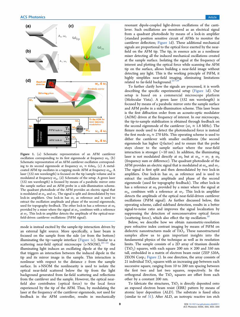
mode is instead excited by the sample-tip interaction driven byan external light source. More specifically, a laser beam isfocused on the sample from the side (or from the bottom)illuminating the tip−sample interface (Figure 1c). Similar to ascattering near-field optical microscope (s-NSOM),20−24 theilluminating light induces an oscillating dipole at the tip endthat triggers an interaction between the induced dipole in thetip and its mirror image in the sample. This interaction isnonlinear with respect to the distance z from the samplesurface. In s-NSOM the nonlinearity is used to isolate theoptical near-field scattered below the tip from the lightbackground generated from far-field scattering and reflectionsfrom the cantilever and the sample. However, the optical near-field also contributes (optical force) to the local forceexperienced by the tip of the AFM. Thus, by modulating thelaser at the frequency of the cantilever eigenmode, not used forfeedback in the AFM controller, results in mechanically
resonant dipole-coupled light-driven oscillations of the canti-lever. Such oscillations are monitored as an electrical signalfrom a quadrant photodiode by means of a lock-in amplifier(standard position sensitive circuit of AFMs to monitor thecantilever deflection; Figure 1d). These additional mechanicalsignals are proportional to the optical force exerted by the near-field on the AFM tip. The tip, in essence acts as a nonlinearmixer detecting all the induced mechanical oscillations createdat the sample surface. Isolating the signal at the frequency ofinterest and plotting the optical force while scanning the AFMtip on the surface, allows building a near-field image withoutdetecting any light. This is the working principle of PiFM, ithighly simplifies near-field imaging, eliminating limitationsrelated to far-field background.25−29
To further clarify how the signals are processed, it is worthdescribing the specific experimental setup (Figure 1d). Oursetup is based on a commercial microscope platform(Molecular Vista). A green laser (532 nm wavelength) isfocused by means of a parabolic mirror onto the sample surfaceand AFM probe in a side-illumination scheme. This laser beamis the first diffraction order from an acousto-optic modulator(AOM) driven at the frequency of interest. In our microscope,the tip-to-sample stabilization is obtained through feedback onthe second eigenmode of the cantilever (ω1 ≈ 1.8 MHz). Theflexure mode used to detect the photoinduced force is insteadthe first mode ω0 ≈ 270 kHz. This operating scheme is used todither the cantilever with smaller oscillations (the secondeigenmode has higher Q-factor) and to ensure that the probestays closer to the sample surface where the near-fieldinteraction is stronger (∼10 nm). In addition, the illuminatinglaser is not modulated directly at ω0 but at ωm = ω1 ± ω0(frequency sum or difference). The quadrant photodiode of theAFM provides an electric signal that is modulated at ωm and ω1.The signal is first split and then demodulated by two lock-inamplifiers. One lock-in has ω1 as reference and is used toextract the oscillation amplitude and phase of the secondeigenmode (used for topography feedback). The other lock-inhas a reference at ω0 provided by a mixer where the signal atωm combines with a reference at ω1. This lock-in amplifierdetects the amplitude of the optical near-field-driven cantileveroscillations (PiFM signal). As further discussed below, thisoperating scheme, called sideband detection, results in a bettersignal-to-noise ratio and improves the signal localization bysuppressing the detection of nonconservative optical forces(scattering force), which also effect the tip oscillation.30
Below, we describe how we obtain nanometric-resolutionpure refractive index contrast imaging by means of PiFM ondielectric nanostructures made of TiO2. These nanostructuredsamples allow us to gain important insights into thefundamental physics of the technique as well as its resolutionlimits. The sample consists of a 2D array of titanium dioxide(TiO2) squares, with each square 200 nm × 200 and 350 nmtall, embedded in a matrix of electron beam resist (ZEP 520A,ZEON Corp.; Figure 2). In one direction, the array consists of21 individual TiO2 squares with an increasing gap between eachsuccessive square, ranging from 10 to 200 nm spacing betweenthe first two and last two squares, respectively. In theorthogonal direction, the TiO2 squares are offset from eachother by a constant 200 nm.To fabricate the structures, TiO2 is directly deposited onto
an exposed electron beam resist (EBR) pattern by means ofatomic layer deposition (ALD). The substrate is fused silica(similar to ref 31). After ALD, an isotropic reactive ion etch
Figure 1. (a) Schematic representation of an AFM cantileveroscillation corresponding to its first eigenmode at frequency ω0. (b)Schematic representation of an AFM cantilever oscillation correspond-ing to its second eigenmode at frequency ω1 ≈ 6.6ω0. (c) A metal-coated AFM tip oscillates in a tapping mode AFM at frequency ωtip. Alaser (532 nm wavelength) is focused on the tip/sample volume and ismodulated at frequency ωm. (d) Schematic of the setup. A green laser(532 nm wavelength) is focused by means of a parabolic mirror ontothe sample surface and an AFM probe in a side-illumination scheme.The quadrant photodiode of the AFM provides an electric signal thatis modulated at ωm and ω1. The signal is split and demodulated by twolock-in amplifiers. One lock-in has ω1 as reference and is used toextract the oscillation amplitude and phase of the second eigenmode,used for topography feedback. The other lock-in has a reference at ω0provided by a mixer where the signal at ωm combines with a referenceat ω1. This lock-in amplifier detects the amplitude of the optical-near-field-driven cantilever oscillations (PiFM signal).
ACS Photonics Article
DOI: 10.1021/acsphotonics.6b00911ACS Photonics XXXX, XXX, XXX−XXX
B

step then follows to produce a nearly planar array of TiO2structures in the electron beam resist matrix. However, in orderto ensure that the TiO2 film overlayer deposited during theALD step is completely removed and only the squares of TiO2and EBR remain, the sample is typically overetched by nominal10−20 nm. This overetching causes in fact the tops of the TiO2squares to be slightly recessed with respect to the height of theEBR (see cross section in Figure 2b). This results in shallowhemispherical indentations in the surface morphology clearlyseen in AFM topography (Figure 2c), where the squaredstructures of the TiO2 are not visible. SEM micrographs of thesame sample show the TiO2 squares embedded in the ZEPmatrix (Figure 2d). The ZEP and TiO2 have very differentcontrast responses to the electron beam. This allows one tomeasure the effective sizes of the TiO2 squares that are 230 nm× 230 nm, 170 nm space between two rows (Figure 2d).Figure 3 shows the PiFM signal (amplitude of the optical-
near-field-driven tip oscillation) image of our TiO2 sample.Although the topography (collected simultaneously) cannotshow the square nature of the TiO2 structures, the PiFM imageclearly shows the correct shape (and size) of the nanostruc-tures, highlighting the TiO2 features, whose refractive index at532 nm wavelength is nTiO2
= 2.428, much higher than that ofthe EBR, whose refractive index is nEBR = 1.56 (note: both TiO2and ZEP have transmission higher than 87% at this wavelength,there is no intrinsic adsorption in this sample at 532 nm).31 Infact, the time average optically driven force that originates thePiFM signal in sideband modulation can be approximatelydescribed as an interaction between the dipole induced at thetip end and its image-dipole in the sample18,19 (Figure 1c).Under the assumption that the illuminating optical field isconstant in the tip−sample surface region (distance below 10nm) the local optical force (gradient force) can beapproximated by the formula:32
α α≈ * | |FZ
E1
Re{ } zpot 4 s t2
(1)
This formula reveals the main features of the local photo-induced force: the interaction is highly nonlinear and dependson z−4 (z is the distance between the tip and the sample); the
strength of the interaction depends upon the polarizability ofboth the tip (αt) and the sample (αs). This means that, oncethe tip material is fixed (we used platinum-coated tips), theinteraction depends on the local material optical constants.This mechanism is responsible for the refractive index contrastshown in the PiFM image of Figure 3. The insert of Figure 3shows a zoomed image of the gap between two squared TiO2structures. A gap as small as 35 nm is clearly distinguishable.It is worth noting that the TiO2 refractive index at λ = 532
nm is ≈1.6× that of ZEP. The PiFM signal from TiO2 is instead≈0.8× that obtained from the electron beam resist (in Figure 3,the features with higher refractive index (TiO2 squares) showthe lower PiFM signal). In fact, there are several conditionsaffecting the sign and strength of the contrast when operatingPiFM in sideband modulation. Operating in direct mode, thatis, when the modulation frequency of the illuminating laserdirectly matches the frequency of one of the eigenmodes of the
Figure 2. (a) Sample consists of an array of titanium dioxide (TiO2) squares embedded in a matrix of electron beam resist (ZEP 520A, ZEONCorp.) on a fused silica substrate. In one direction, the array consists of 21 individual TiO2 squares with an increasing gap between each successivesquare. In the orthogonal direction the TiO2 squares are offset from each other by a constant distance. (b) Cross section of the TiO2 structures. Thesample is typically overetched by nominal 10−20 nm. This results into shallow hemispherical troughs in the surface morphology clearly seen in AFMtopography (c). (d) SEM micrographs of the same sample showing the TiO2 squares embedded in the ZEP matrix. From the SEM image, the TiO2squares are 230 nm × 230 nm, with 170 nm space between two rows.
Figure 3. PiFM image of the TiO2 squares embedded in ZEPphotoresist. The PiFM signal is the amplitude from the lock-inamplifier demodulating at the first eigenmode frequency ω0. Thesecond eigenmode of the cantilever is instead used to retrieve thesample morphology and for tip-to-sample distance stabilization. Thetwo materials have different refractive indices and are almostcompletely transparent to the illuminating light. Here the materialwith higher refractive index produces the lower PiFM signal. Thefigure’s inset shows the PiFM image of a gap of 35 nm between twoTiO2 squared structures.
ACS Photonics Article
DOI: 10.1021/acsphotonics.6b00911ACS Photonics XXXX, XXX, XXX−XXX
C

cantilever, it has been shown that quantitative information onthe forces can be retrieved through fitting of force−distancecurves.18 As extensively discussed in ref 32, operating in direct-mode, has the drawback that at least another light-driven force,a nonlocal force (scattering force) is effective, producing anoverall background to the signal of interest. In sidebandmodulation instead, the detection becomes sensitive almostexclusively to the local force described in eq 1.33,34 Thisoperating mode improves the signal-to-noise ratio allowing thehigh resolution imaging that we show here, but it makesdifficult to absolutely quantify the detected signal. In fact insideband modulation, where the laser modulation frequency iseither ωm = ω1 + ω0 or ωm = ω1 − ω0, the optically inducedoscillations on the tip also result in the modulation of the localforce gradient (the gradient of the total local interaction forceF, including mechanical (van der Waals, etc.) and opticallyinduced forces) at the same frequency ωm. The force gradientmodulation induces a frequency shift (ω → ω′) on thecantilever oscillation frequency according to the relation validfor small perturbations:18
ω′ = − ∂∂
⎜ ⎟⎛⎝
⎞⎠k
Fz
m/(2)
where m is the effective mass and k is the effective stiffness(force constant) of the cantilever eigenmode. The continuousmodulation of the force gradient at ωm results in a frequencymodulation which, together with the nonlinearity of the tip−sample interaction with the distance from the surface, producessidebands at ω1 ± ωm. In sideband modulation, ω1 ± ωm isadjusted to match one of the eigenmodes of the cantilever (thefirst mode in our experiment) and the PiFM signal is thendominated by the gradient of force in eq 1. This is actually whyin sideband modulation the contribution of the scattering forceis minimized. The scattering force is constant with respect tothe tip−sample distance z and its gradient (derivative withrespect to z) is in fact null. Reducing the nonlocal scatteringforce to negligible values strongly reduces the background andincrease the signal-to-noise ratio.However, the forces that contribute to the cantilever
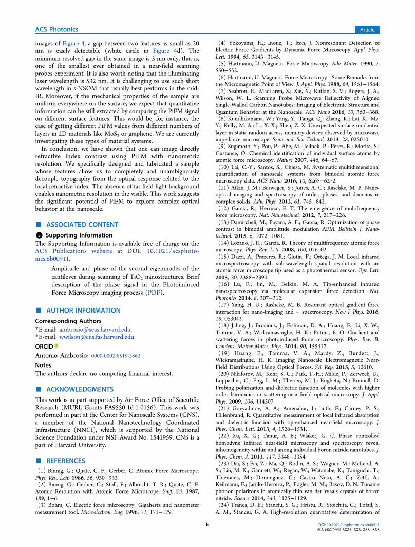
frequency shift described by eq 2 include also forces like vander Waals that depend on the material. As a result, the overallresonance frequency shift on one material can be different thanthat on another material. This may in practice influence thecontrast in PiFM in a distinctive way. Figure 4 illustrates thisconcept. For this experiment, we used a standard glass coverslipthat has unknown nanoparticles on its surface resulting fromfabrication. Figure 4a shows the PiFM signal as a function ofthe illuminating laser modulation frequency. More precisely,the laser modulation is tuned around ωm = ω1 − ω0. The AFMtopographical image of the sample surface is showed in Figure4c. The free oscillation amplitude of the second eigenmode ofthe cantilever is less than 20 nm. The red curve in Figure 4ashows the PiFM signal vs demodulating frequency when theAFM feedback set point is at 81% (this means that theoscillation amplitude of the tip engaged with the surface isabout 81% of the free oscillation amplitude) and the tip is onthe glass coverslip. Note that the laser modulation frequency isalso tuned accordingly. The blue curve in the same imageshows instead the same signal when the tip is on one of theparticles. In this case, the two peaks are shifted by only 2.7 kHzand the two curves are almost superimposed. Choosing eitherthe peak of the blue or the red curve of Figure 4a as
demodulation frequency does not really matter in theseconditions and it always results in a contrast where the PiFMsignal is lower on the particles than on the glass (Figure 4d).The contrast condition is quite different when the set point is
changed from 81% to 67% (smaller tip−sample distance).Figure 4b shows the same curves of Figure 4a at this newworking distance. Now, the red and blue curves, although quitesimilar in peak amplitudes, are shifted by 6.3 kHz. The twocurves cross around 278 kHz. This means that when thedemodulation frequency for the PiFM signal is set above 278kHz, when the tip is on the particles the PiFM signal can behigher than when the tip is on the glass. This, in fact, resultsinto a reversed contrast in the PiFM image, as shown in Figure4e. When the lock-in demodulation frequency is set below 278kHZ, the same contrast as in Figure 4d is re-established.The possibility of reversing the contrast in PiFM imaging
clearly shows that it is not possible, in such experimentalconditions (sideband modulation), to extract any detailedquantitative information from the PiFM values on the opticalparameters of the material. However, controlling the PiFMdemodulation frequency, as described here, allows one to setconditions that maximize the contrast. This is crucial in imagingfeatures like sharp edges shown in Figure 3 or small particleslike those of Figure 4. It is worth noting that, in the PiFM
Figure 4. (a) PiFM signal as a function of the lock-in demodulatingfrequency (around the first eigenmode resonance). The red curve in(a) shows the PiFM vs demodulating frequency when the AFMfeedback set point is at 81% and the tip is on the glass coverslip. Theblue curve in the same image shows instead the same curve when thetip is on one of the particles. (b) Same as for (a) when the set point is67%. (c) AFM topographical image of the sample surface. (d) PiFMimage obtained when operating with 81% set point. (e) PiFM imageobtained when the set point is changed to 67% and the lasermodulation frequency and the lock-in demodulation frequency areboth above 278 kHz.
ACS Photonics Article
DOI: 10.1021/acsphotonics.6b00911ACS Photonics XXXX, XXX, XXX−XXX
D
images of Figure 4, a gap between two features as small as 20nm is easily detectable (white circle in Figure 4d). Theminimum resolved gap in the same image is 5 nm only, that is,one of the smallest ever obtained in a near-field scanningprobes experiment. It is also worth noting that the illuminatinglaser wavelength is 532 nm. It is challenging to use such shortwavelength in s-NSOM that usually best performs in the mid-IR. Moreover, if the mechanical properties of the sample areuniform everywhere on the surface, we expect that quantitativeinformation can be still extracted by comparing the PiFM signalon different surface features. This would be, for instance, thecase of getting different PiFM values from different numbers oflayers in 2D materials like MoS2 or graphene. We are currentlyinvestigating these types of material systems.In conclusion, we have shown that one can image directly
refractive index contrast using PiFM with nanometricresolution. We specifically designed and fabricated a samplewhose features allow us to completely and unambiguouslydecouple topography from the optical response related to thelocal refractive index. The absence of far-field light backgroundenables nanometric resolution in the visible. This work suggeststhe significant potential of PiFM to explore complex opticalbehavior at the nanoscale.
■ ASSOCIATED CONTENT
*S Supporting InformationThe Supporting Information is available free of charge on theACS Publications website at DOI: 10.1021/acsphoto-nics.6b00911.
Amplitude and phase of the second eigenmodes of thecantilever during scanning of TiO2 nanostructures. Briefdescription of the phase signal in the PhotoinducedForce Microscopy imaging process (PDF).
■ AUTHOR INFORMATION
Corresponding Authors*E-mail: [email protected].*E-mail: [email protected].
ORCIDAntonio Ambrosio: 0000-0002-8519-3862NotesThe authors declare no competing financial interest.
■ ACKNOWLEDGMENTS
This work is in part supported by Air Force Office of ScientificResearch (MURI, Grants FA9550-16-1-0156). This work wasperformed in part at the Center for Nanoscale Systems (CNS),a member of the National Nanotechnology CoordinatedInfrastructure (NNCI), which is supported by the NationalScience Foundation under NSF Award No. 1541959. CNS is apart of Harvard University.
■ REFERENCES(1) Binnig, G.; Quate, C. F.; Gerber, C. Atomic Force Microscope.Phys. Rev. Lett. 1986, 56, 930−933.(2) Binnig, G.; Gerber, C.; Stoll, E.; Albrecht, T. R.; Quate, C. F.Atomic Resolution with Atomic Force Microscope. Surf. Sci. 1987,189, 1−6.(3) Bohm, C. Electric force microscopy: Gigahertz and nanometermeasurement tool. Microelectron. Eng. 1996, 31, 171−179.
(4) Yokoyama, H.; Inoue, T.; Itoh, J. Nonresonant Detection ofElectric Force Gradients by Dynamic Force Microscopy. Appl. Phys.Lett. 1994, 65, 3143−3145.(5) Hartmann, U. Magnetic Force Microscopy. Adv. Mater. 1990, 2,550−552.(6) Hartmann, U. Magnetic Force Microscopy - Some Remarks fromthe Micromagnetic Point of View. J. Appl. Phys. 1988, 64, 1561−1564.(7) Seabron, E.; MacLaren, S.; Xie, X.; Rotkin, S. V.; Rogers, J. A.;Wilson, W. L. Scanning Probe Microwave Reflectivity of AlignedSingle-Walled Carbon Nanotubes: Imaging of Electronic Structure andQuantum Behavior at the Nanoscale. ACS Nano 2016, 10, 360−368.(8) Kundhikanjana, W.; Yang, Y.; Tanga, Q.; Zhang, K.; Lai, K.; Ma,Y.; Kelly, M. A.; Li, X. X.; Shen, Z. X. Unexpected surface implantedlayer in static random access memory devices observed by microwaveimpedance microscope. Semicond. Sci. Technol. 2013, 28, 025010.(9) Sugimoto, Y.; Pou, P.; Abe, M.; Jelinek, P.; Perez, R.; Morita, S.;Custance, O. Chemical identification of individual surface atoms byatomic force microscopy. Nature 2007, 446, 64−67.(10) Lai, C.-Y.; Santos, S.; Chiesa, M. Systematic multidimensionalquantification of nanoscale systems from bimodal atomic forcemicroscopy data. ACS Nano 2016, 10, 6265−6272.(11) Atkin, J. M.; Berweger, S.; Jones, A. C.; Raschke, M. B. Nano-optical imaging and spectroscopy of order, phases, and domains incomplex solids. Adv. Phys. 2012, 61, 745−842.(12) Garcia, R.; Herruzo, E. T. The emergence of multifrequencyforce microscopy. Nat. Nanotechnol. 2012, 7, 217−226.(13) Damircheli, M.; Payam, A. F.; Garcia, R. Optimization of phasecontrast in bimodal amplitude modulation AFM. Beilstein J. Nano-technol. 2015, 6, 1072−1081.(14) Lozano, J. R.; Garcia, R. Theory of multifrequency atomic forcemicroscopy. Phys. Rev. Lett. 2008, 100, 076102.(15) Dazzi, A.; Prazeres, R.; Glotin, F.; Ortega, J. M. Local infraredmicrospectroscopy with sub-wavelength spatial resolution with anatomic force microscope tip used as a photothermal sensor. Opt. Lett.2005, 30, 2388−2390.(16) Lu, F.; Jin, M.; Belkin, M. A. Tip-enhanced infrarednanospectroscopy via molecular expansion force detection. Nat.Photonics 2014, 8, 307−312.(17) Yang, H. U.; Rashcke, M. B. Resonant optical gradient forceinteraction for nano-imaging and − spectroscopy. New J. Phys. 2016,18, 053042.(18) Jahng, J.; Brocious, J.; Fishman, D. A.; Huang, F.; Li, X. W.;Tamma, V. A.; Wickramasinghe, H. K.; Potma, E. O. Gradient andscattering forces in photoinduced force microscopy. Phys. Rev. B:Condens. Matter Mater. Phys. 2014, 90, 155417.(19) Huang, F.; Tamma, V. A.; Mardy, Z.; Burdett, J.;Wickramasinghe, H. K. Imaging Nanoscale Electromagnetic Near-Field Distributions Using Optical Forces. Sci. Rep. 2015, 5, 10610.(20) Nikiforov, M.; Kehr, S. C.; Park, T.-H.; Milde, P.; Zerweck, U.;Loppacher, C.; Eng, L. M.; Therien, M. J.; Engheta, N.; Bonnell, D.Probing polarization and dielectric function of molecules with higherorder harmonics in scattering-near-fireld optical microscopy. J. Appl.Phys. 2009, 106, 114307.(21) Govyadinov, A. A.; Amenabar, I.; huth, F.; Carney, P. S.;Hillenbrand, R. Quantitative measurement of local infrared absorptionand dielectric function with tip-enhanced near-field microscopy. J.Phys. Chem. Lett. 2013, 4, 1526−1531.(22) Xu, X. G.; Tanur, A. E.; Wlaker, G. C. Phase controlledhomodyne infrared near-field microscopy and spectroscopy revealinhomogeneity within and anong individual boron nitride nanotubes. J.Phys. Chem. A 2013, 117, 3348−3354.(23) Dai, S.; Fei, Z.; Ma, Q.; Rodin, A. S.; Wagner, M.; McLeod, A.S.; Liu, M. K.; Gannett, W.; Regan, W.; Watanabe, K.; Taniguchi, T.;Thiemens, M.; Dominguez, G.; Castro Neto, A. C.; Zettl, A.;Keilmann, F.; Jarillo-Herrero, P.; Fogler, M. M.; Basov, D. N. Tunablephonon polaritons in atomically thin van der Waals crystals of boronnitride. Science 2014, 343, 1125−1129.(24) Tranca, D. E.; Stanciu, S. G.; Hristu, R.; Stoichita, C.; Tofail, S.A. M.; Stanciu, G. A. High-resolution quantitative determination of
ACS Photonics Article
DOI: 10.1021/acsphotonics.6b00911ACS Photonics XXXX, XXX, XXX−XXX
E

dielectric function by using scattering scanning near-field opticalmicroscopy. Sci. Rep. 2015, 5, 11876.(25) Rajapaksa, I.; Uenal, K.; Wickramasinghe, H. K. Image forcemicroscopy of molecular resonance: A microscope principle. Appl.Phys. Lett. 2010, 97, 073121.(26) Rajapaksa, I.; Kumar Wickramasinghe, H. Raman spectroscopyand microscopy based on mechanical force detection. Appl. Phys. Lett.2011, 99, 161103.(27) Jahng, J.; Fishman, D. A.; Park, S.; Nowak, D. B.; Morrison, W.A.; Wickramasinghe, H. K.; Potma, E. O. Linear and nonlinear opticalspectroscopy at the nanoscale with photoinduced force microscopy.Acc. Chem. Res. 2015, 48, 2671−2679.(28) Jahng, J.; Brocious, J.; Fishman, D. A.; Yampolsky, S.; Nowak,D.; Huang, F.; Apkarian, V. A.; Wickramasinghe, H. K.; Potma, E. O.Ultrafast pump-probe force microscopy with nanoscale resolution.Appl. Phys. Lett. 2015, 106, 08113.(29) Jang, J.; Ladani, F. T.; Khan, R. M.; Li, X.; Lee, E. S.; Potma, O.E. Visualizing surface plasmon polaritons by their gradient force. Opt.Lett. 2015, 40, 5058−5061.(30) Gomez, C. J.; Garcia, R. Determination and simulation ofnanoscale energy dissipation processes in amplitude modulation AFM.Ultramicroscopy 2010, 110, 626−633.(31) Devlin, R. C.; Khorasaninejad, M.; Chen, W. T.; Oh, J.; Capasso,F. Broadband high-efficiency dielectric metasurfaces for the visiblespectrum. Proc. Natl. Acad. Sci. U. S. A. 2016, 113, 10473−10478.(32) Nowak, D.; Morrison, W.; Wickramasinghe, H. K.; Jahng, J.;Potma, E.; Wan, L.; Ruiz, R.; Albrecht, T. R.; Schmidt, K.; Frommer,J.; Sanders, D. P.; Park, S. Nanoscale chemical imaging byphotoinduced force microscopy. Science Advances 2016, 2, e1501571.(33) Wagner, T.; Beyer, H.; Reissner, P.; Mensch, P.; Riel, H.;Gotsmann, B.; Stemmer, A. Kelvin probe force microscopy for localchracterization of sctive nanoelectronic devices. Beilstein J. Nanotechnol.2015, 6, 2193−2206.(34) Jahng, J.; Kim, B.; Lee, S. E.; Potma, E. O. Quantitative aalysis ofsideband coupling in photoinduced force microscopy. Phys. Rev. B:Condens. Matter Mater. Phys. 2016, 94, 195407.
ACS Photonics Article
DOI: 10.1021/acsphotonics.6b00911ACS Photonics XXXX, XXX, XXX−XXX
F