oeb univ. publish. co. elaboration and characterization of ... · elaboration and characterization...
TRANSCRIPT
Elaboration and characterization of zinc oxide varistors
A. Bouchekhlal a, Y. Beggah b, M.S. Aidab aMaterials Research Laboratory, Faculty of Engineering Science, Physics Department. University of Jijel, 1800 Algeria.
bLaboratory for Thin Film and Interface, Science Faculty, Department of Physics, University of Constantine Mantouri, 2500 Algeria. E-mail : [email protected]
Received: 23 May 2011, accepted: 30 September 2011 Abstract
ZnO-based varistors were fabricated by sintering zinc oxide micro crystals with several additives of metal Oxides. The effect of sintering temperature on varistor properties of (Bi, Co, Cr, Mn, Sb, Al)-doped ZnO ceramics was investigated in the range of 1280–1350 °C. The average grain size increased to 5.13 to 7.88 µm with the increase of sintering temperature. However, the nonlinear coefficient of this system was nearly constant in the range of sintering temperature. The highest breakdown voltage was 1143.4 v / cm for the varistor sintered at 1350 °C the sample C sintered exhibited the best electrical properties. Keywords: ZnO; Microstructure; Electrical properties; Varistors 1. Introduction:
ZnO varistors have been widely used as surge protection devices due to their highly nonlinear current–voltage (I–V) characteristics in the normal case, varistors are subjected to a voltage below their characteristic breakdown and pass only a leakage current. When the voltage exceeds the breakdown voltage during voltage fluctuations, the varistor becomes highly conducting and draws current through it, usually to ground. When the voltage returns to normal, the varistor returns to its highly resistive state. [1] Zinc oxide (ZnO) varistors are formed by sintering mixture of ZnO powders with small amounts of other oxides, such as Bi2O3, Sb2O3, Al2O3, MnO2, Cr2O3, etc., the relationship between the voltage across the terminal, V, and the current in the devices, I, is typically expressed by I = kV α. The term α in the equation is a nonlinear coefficient, inherent parameter of varistors representing the degree of nonlinearity of conduction. It is very important to comprehend the influence of the sintering process on varistor properties. The influence of sintering temperature on varistor properties is different with existing compositions of ceramics. [2]
The purposes of the present study are to develop the ZnO-based ceramic varistors. In this work, ZnO-based ceramic varistors with more than five additives of metal oxides have been fabricated. The microstructure of the varistors were studied using scanning electron microscopy (SEM) and X-ray diffraction(XRD) analysis and the properties of the ZnO based ceramic for use as varistors were discussed on the basis of the measurements of V(I) and C(V) characteristics. 2. Experimental procedure 2.1. Sample preparation
ZnO– Bi2O3-based varistor samples with a nominal composition of 97.2 mol.% ZnO, 0.5 mol.% Bi2O3, 1.0 mol.% Sb2O3, 0.3 mol.% Al2O3, 0.5 mol.% Cr2O3, and 0.5 mol.% MnO2 were used, samples (B). Reagent-grade raw materials were pulverized by an agate mortar/pestle for 1h. Reagent-grade raw materials were used for preparing the varistor (C) of 98 mol.% ZnO, 0.5 mol.% Bi2O3, 1.0 mol.% Sb2O3, 0.5 mol.% Cr2O3, Reagent-grade raw materials were mixed and homogenized in absolute ethanol media in a
polyethylene bowl with zirconia balls for 24 h. After milling, the mixture was calcined in air at 750 °C for 2 h. [3] The calcined powders were pressed into discs of 13 mm in diameter and 1 mm thickness at a pressure of 1000 kg/cm2. The discs were sintered at four fixed sintering temperatures 1280 °C, 1300 °C, 1320 °C, and 1350°C in air for 1 h in a furnace (Nabertherm, MORE THAN HEAT 30-3000 °C), at a heating rate of 5 °C/min and then cooled in the furnace. Finally, the surfaces of the sintered Samples were grinded and covered with silver paste to obtain electrodes. [4]
2.2. Characterization
The microstructure was examined by a scanning electron microscope PHILIPS (XL 30). The average grain size (d) of the ceramics was determined by the linear intercept method , given by d = 1.56L/MN,[5] where L is the random line length on the micrograph, M is the magnification of the micrograph, and N is the number of the grain boundaries intercepted by lines. [6] The crystalline phases were identified by an X-ray diffractometry (BRUKER - AXS type D8) with CuKα radiation. The electric field–current density (E–J) characteristics were measured using a V–I source (TEKTRONIX 370) The breakdown field (E1mA/cm2) was measured at 1.0mA/cm2 and the leakage current density (JL) was measured at 0.8 E1mA/cm2 In addition, the nonlinear coefficient (α) is defined by the empirical law, J = CEα where J is the current density, E is the applied electric field, and C is the constant. ˛ was determined in the current density range of 1mA/cm2 to 10mA/cm2, where 1 ⁄ , and E1 and E2 are the electric fields corresponding to 1.0mA/cm2 and10mA/cm2, respectively. The capacitance–voltage (C–V) characteristics were measured at 1 MHz as test frequency using an RLC meter (KEITHLE 590). The donor concentration (Nd) and the barrier height (Φb) were determined by the equation 1 1 2⁄⁄ = 2( / where Cb is the capacitance per unit area of a grain boundary, Cbo is the value of Cb when Vgb=0, Vgb is the applied voltage per grain boundary, q is the electronic charge, ε is the permittivity of ZnO (ε=8.5εo). [7]
Journal of New Technology and Materials JNTM
Vol. 01, N°00 (2011)51-54 OEB Univ. Publish. Co.
3.
diffpeaobtsecthe144
varno Znsin
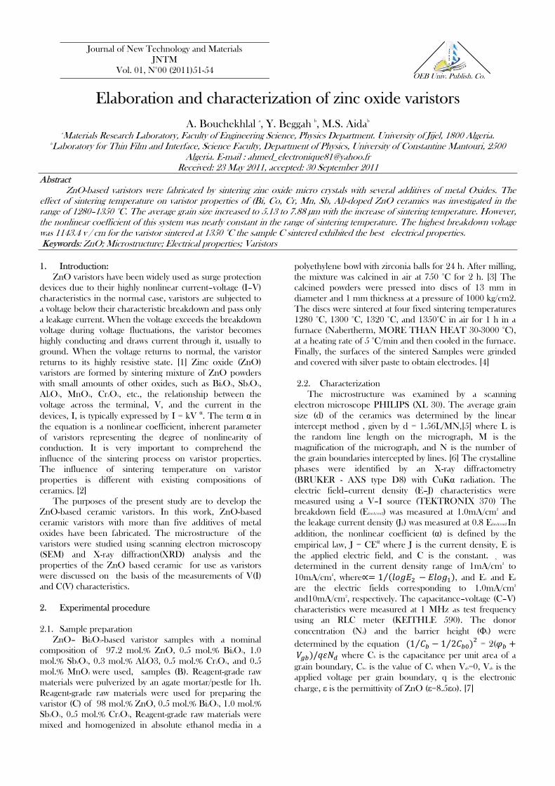
Results and Fig. 1 s
fferent sinterinaks correspontained (JCPDcondary peakse Bi2O3 phas49, respective
20
0500
10001500200020
0500
100015002000
unte
nsité
(u.a
)
20
0500
100015002000
20
0500
100015002000
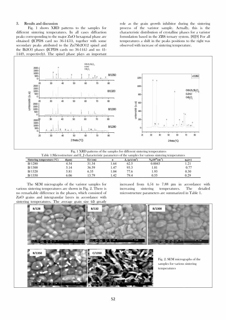
Sintering teB/1280 B/1300 B/1320 B/1350 The SEM
rious sintering remarkable d
nO grains andtering temper
B/128
B/1350
d discussion shows XRD ng temperatu
nding to the maDS card no 3s attributed toses (JCPDS cely). The spin
30
0 00
30 4
30
30
00
0
Table 1:Microsemperature (°C)
M micrograph temperatures
difference in thd intergranularatures. The
0
patterns to tures. In all cajor ZnO hexa
36-1451), togeo the Zn7Sb2cards no 36-14nel phase play
40 50
00
2 theta (°C
40 50
40 50
40 50
00
Fig. 1 XRstructure and E_ d(µm) 4.54 5.14 5.81 6.06
hs of the variss are shown inthe phases, whar layers in aaverage grain
the samples fcases diffractiagonal phase a
ether with som2O12 spinel a445 and no 4ys an importa
60 70
00
C)
60 70
60 70
60 70
O-B-Zn7Sb2O120-ZnO0-Bi2O3
000
0
00
RD patterns of _J characteristic E(v/cm) 31.34 36.59 6.35 13.79
stor samples fn Fig. 2. Therehich consistedaccordance w size (d) grea
B/132
C/1350
52
for ion are me and 41-ant
roprchfoteob
80
B/1280
80
B/1300
80
B/1320
80
B/13500
the samples forc parameters of α
1.64 1.47 1.04 1.42
for e is of
with atly
ininm
ole as the grrocess of thharacteristic diormulation basmperatures a bserved with in
20
0
200
400
600
800
1000
1200
unte
nsité
(u.a
)
r different sinter the samples for JL (µA/cm2) 62.5 93.3 77.6 79.4
ncreased fromncreasing simicrostructure p
rain growth ie varistor saistribution of csed in the ZB shift in the pncrease of sint
0 30 40
0 00
00
ring temperaturr various sinterin Nd(1018cm-3) 0.0043 1.01
1.93 0.55
m 4.54 to 7ntering temparameters ar
B/1300
Fig. samtemp
inhibitor duriample. Actuacrystalline phaS ternary syste
peaks positionstering tempera
50 60
000 0
0
00
0
0
2 theta (°C)
res ng temperature
7.88 µm in mperatures. e summarized
2. SEM microgmples for various
peratures
ing the sinteally, this is ases for a variem. [8][9] Fors to the right ature.
70 80
0000
0
00
O-B-Zn7Sb2O120-ZnO0-Bi2O3
c/1350
s φb(ev) 1.21 0.77 0.30
0.29
accordance wThe deta
d in Table 1.
graphs of the s sintering
ring the
istor r all was
with ailed
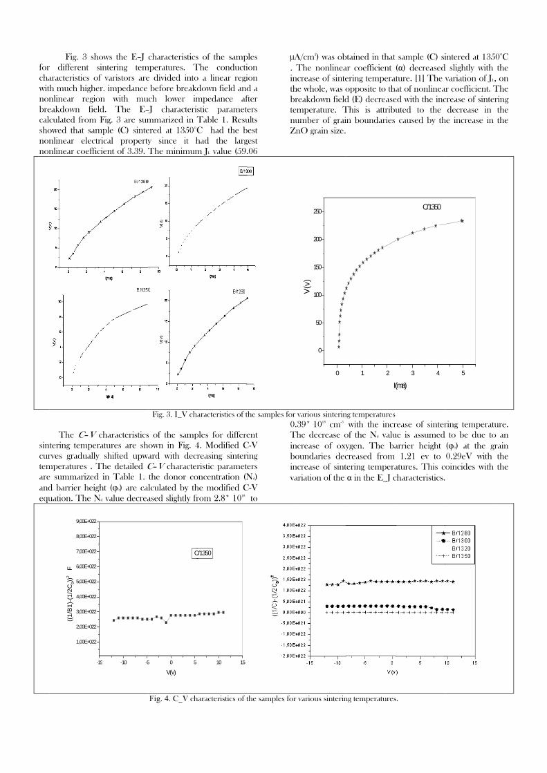
forchawitnonbrecalcshononnon
sincurtemareandequ
Fig. 3 shr different saracteristics ofth much highenlinear regioeakdown fielculated from owed that samnlinear electrnlinear coeffic
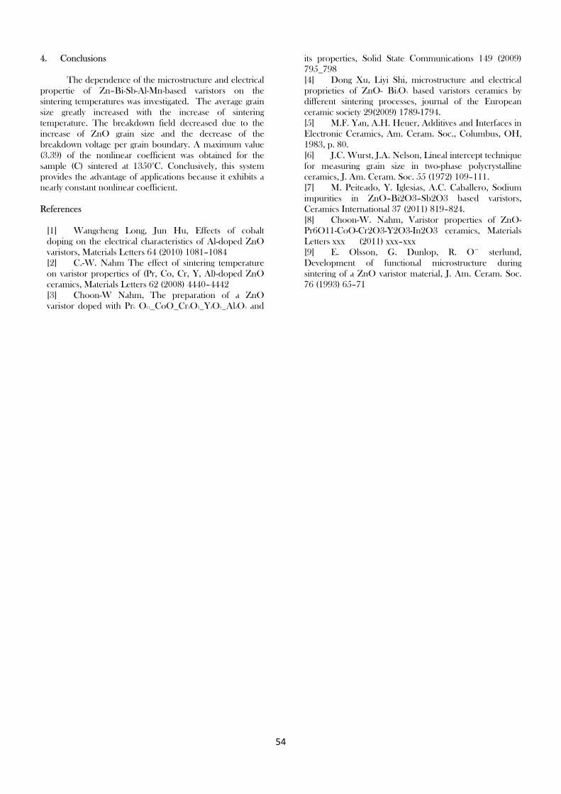
The C–V tering temperrves graduallymperatures . Te summarizedd barrier heiguation. The N
1,00E+022
2,00E+022
3,00E+022
4,00E+022
5,00E+022
6,00E+022
7,00E+022
8,00E+022
9,00E+022
-1
((1/
B1)
-(1/
2C0))
2 F
ows the E–J sintering temf varistors are
er. impedance on with muld. The E–Fig. 3 are sum
mple (C) sinterical propertycient of 3.39. T
characteristicsratures are shy shifted upwaThe detailed C in Table 1.
ght (φb) are calNd value decrea
15 -10 -5
characteristicsmperatures. Te divided into before breakdch lower im
–J characterismmarized in Tered at 1350°Cy since it hThe minimum
Fig. 3. I_V cha
s of the sampown in Fig. 4ard with decrC–V characterthe donor colculated by thased slightly fr
5 0 5
V(v)
C
Fig. 4. C_V ch
s of the sampThe conductio a linear regidown field andmpedance afstic parameteTable 1. ResuC had the bhad the largm JL value (59.
aracteristics of t
ples for differe4. Modified Creasing sinteriristic paramete
oncentration (Nhe modified Crom 2.8* 1018
10 15
C/1350
haracteristics of t
ples ion ion d a fter ters ults best gest .06
µA. TinthbrtenuZn
the samples for
ent C-V ing ters Nd)
C-V to
0.Thinboinva
the samples for
A/cm2) was obThe nonlinea
ncrease of sintehe whole, was oreakdown fieldmperature. Tumber of grainO grain size.
0
0
50
100
150
200
250
V(v
)
various sinterin39* 1018 cm-3
he decrease oncrease of oxyoundaries dec
ncrease of sintariation of the
various sinterin
btained in thatar coefficient ering temperaopposite to thd (E) decreaseThis is attribuin boundaries
1 2
I(
ng temperatures with the incrof the Nd valuygen. The bacreased from tering tempera α in the E_J c
ng temperatures
t sample (C) si(α) decreased
ature. [1] The at of nonlinea
ed with the incuted to the caused by th
3 4
(ma)
C/1350
rease of sinterue is assumedarrier height 1.21 ev to atures. This ccharacteristics.
s.
intered at 135d slightly with variation of JL
ar coefficient. Tcrease of sintedecrease in
he increase in
5
ring temperatud to be due to
(φb) at the g0.29eV with oincides with
50°C the , on The ring the
the
ture. o an rain the
the
54
4. Conclusions
The dependence of the microstructure and electrical propertie of Zn–Bi-Sb-Al-Mn-based varistors on the sintering temperatures was investigated. The average grain size greatly increased with the increase of sintering temperature. The breakdown field decreased due to the increase of ZnO grain size and the decrease of the breakdown voltage per grain boundary. A maximum value (3.39) of the nonlinear coefficient was obtained for the sample (C) sintered at 1350°C. Conclusively, this system provides the advantage of applications because it exhibits a nearly constant nonlinear coefficient. References
[1] Wangcheng Long, Jun Hu, Effects of cobalt doping on the electrical characteristics of Al-doped ZnO varistors, Materials Letters 64 (2010) 1081–1084 [2] C.-W. Nahm The effect of sintering temperature on varistor properties of (Pr, Co, Cr, Y, Al)-doped ZnO ceramics, Materials Letters 62 (2008) 4440–4442 [3] Choon-W Nahm, The preparation of a ZnO varistor doped with Pr6 O11_CoO_Cr2O3_Y2O3_Al2O3 and
its properties, Solid State Communications 149 (2009) 795_798 [4] Dong Xu, Liyi Shi, microstructure and electrical proprieties of ZnO- Bi2O3 based varistors ceramics by different sintering processes, journal of the European ceramic society 29(2009) 1789-1794. [5] M.F. Yan, A.H. Heuer, Additives and Interfaces in Electronic Ceramics, Am. Ceram. Soc., Columbus, OH, 1983, p. 80. [6] J.C. Wurst, J.A. Nelson, Lineal intercept technique for measuring grain size in two-phase polycrystalline ceramics, J. Am. Ceram. Soc. 55 (1972) 109–111. [7] M. Peiteado, Y. Iglesias, A.C. Caballero, Sodium impurities in ZnO–Bi2O3–Sb2O3 based varistors, Ceramics International 37 (2011) 819–824. [8] Choon-W. Nahm, Varistor properties of ZnO-Pr6O11-CoO-Cr2O3-Y2O3-In2O3 ceramics, Materials Letters xxx (2011) xxx–xxx [9] E. Olsson, G. Dunlop, R. O¨ sterlund, Development of functional microstructure during sintering of a ZnO varistor material, J. Am. Ceram. Soc. 76 (1993) 65–71