omm the photonic opal – the jewel c in the crown of ... in the lab opposite, sajeev john. ......
TRANSCRIPT

WHEN it comes to developing newtechnologies, a comment often made isthat chemists and physicists need to talkmore. Focused discussion can open upnew scientific vistas glowing withpotential. This is what Geoffrey Ozinfound when first accosted by his physicistneighbour in the lab opposite, Sajeev John.To those in the know, Professor John is theworld-leading theorist who had, along withEli Yablonovitch, kicked off the fledglingfield of photonic bandgap crystals –materials that are the optical analogues ofsemiconductors. Physicists are excitedabout them because they couldrevolutionise telecommunications and putoptical computing on a sound footing.John had a precise theoretical blueprint formaking a useful photonic crystal. Ozin,together with Francisco Meseguer inValencia, Spain, had the chemicalexperience needed to fabricate it. Theresult was a joint paper in Nature in 2000describing the large-scale synthesis of asilicon photonic crystal with a completethree-dimensional bandgap.2 Three-dimensional photonic crystals had beenmade in silicon using lithography but werejust a few periodic layers thick.3
Photonic bandgapsThe concept of an optical bandgap wasfirst proposed in 1987 by Yablonovitch,4
then at Bell Communications in NewJersey, and independently by John,5 thenat Princeton. The idea somehow seemsobvious now, that – just as the periodicatomic structure of a semiconductorcauses Bragg-like diffraction ofpropagating electrons resulting in aforbidden range of energies, the bandgap –
photons propagating through a periodicdielectric can also scatter and interfere,resulting in a photonic bandgap. Anappealing aspect is that, unlike theSchrödinger equation for interactingelectrons in semiconductors, Maxwell’sequations describing the behaviour of lightin periodic dielectric can be solvedexactly. Furthermore, there is nofundamental scaling length – theperiodicity is not limited to an atomiclattice and can be on any scale.
However, nobody had actually created aphotonic bandgap. What was needed was a
material exhibiting a regular variation indielectric constant, or refractive index – aphotonic crystal (Fig. 1). Yablonovitch’sfirst effort in 1991 involved simply drillinga large-scale 3D array of millimetre-sizedair holes in a slab of material with arefractive index of 3.6. This blocked outlight in the microwave region – notparticularly practical but it created asensation.6
To be useful for communications, thespacing of the photonic lattice needs to becomparable with the wavelength ofinfrared light, at around a micrometre or
Ch
emC
om
mw
ww
.rsc
.org
/ch
em
com
m
F O C U S A R T I C L E
The photonic opal – the jewelin the crown of opticalinformation processingPhotons have many advantages over electrons as carriers of information.They arefaster and can convey huge amounts of data with low power losses. A new class ofmaterials called photonic crystals have the potential to steer light in the same way aselectrons are manipulated in semiconductor chips. Fabricating these devices isproving extremely challenging. Nevertheless, an ingenious chemical approach isbeing exploited by research groups such as that of Geoffrey Ozin at the Universityof Toronto, which may not only contribute to the development of the all-opticalcomputer but also stimulate the expansion of a new field of materials science. NinaHall discusses Professor Ozin’s contribution.
This journa l is © The Roya l Soc iety of Chemistry 2003 CHEM. COMMUN., 2003 2639
DO
I: 10
.103
9/b
3067
71h
Professor Ozin received a BSc in chemistryfrom King’s College London and a DPhil ininorganic chemistry from the University ofOxford in 1967. He was ICI Fellow at theUniversity of Southampton from 1967 to1969 before joining the University ofToronto in 1969; he became full professor in1977 and University Professor in 2001.Professor Ozin is Honorary ProfessorialFellow at The Royal Institution of GreatBritain and University College London, andis a Government of Canada Research Chairin Materials Chemistry.
The focus of Professor Ozin’s materialschemistry research is on supramolecularchemistry (chemistry beyond the molecule),materials self-assembly over all scales(chemistry approaches to inorganicmaterials with complex form), biomimeticinorganic chemistry (copying the chemistry ofbiomineralisation), nanochemistry (chemistry at the nanometre scale), inorganic-organic hybrid materials (chemistry strategies to nanocomposites), inclusioncompounds (host-guest nanomaterials chemistry) and photonic materials chemistry(chemical approaches to control the flow of light).

so. And ideally the photonic crystal shouldbe based on the electronics engineer’s firstlove – silicon, or possibly galliumarsenide. The 1990s saw a surge of activityas physicists and materials scientiststhought up imaginative schemes ofmicrofabrication to make photonicmaterials with the right scale-lengths.There have been some successes, mostlyin one and two dimensions. Ingeniously-made optical fibres with a one-dimensionalphotonic bandgap look promising forcarrying more data,7 but materials with atwo-dimensional bandgap are not likely tobe practical as they leak light from thethird dimension.
One of the problems is that the requiredphotonic lattice-scale is difficult to reachusing the traditional top-down fabricationmethods of the semiconductor industry.Here, however, something can be learntfrom Nature who, as ever, mastered theassembly of photonic materials first – iniridescent butterfly wings, in the hairs ofthe sea mouse and even in the scales of theancient coelacanth. Significantly, theshimmering colours of the opal are due toa partial photonic bandgap caused by theclose-packing of silica spheres, a fractionof a micrometre across.
Microengineering opalstructuresChemists, of course, are adept atexploiting the same natural principlesthrough which directed self-assemblyachieves a precise matching of structuralcomplexity to application. Indeed, the opal
structure concept,combined with clever butestablished chemicalmanipulation, soonsuggested a promisingapproach to making 3Dphotonic lattices. In 1998,two research groups, oneat the University ofMinnesota and one at theUniversity of Amsterdam,had prepared opal-likeporous materials withphotonic crystalcharacteristics.8,9 Theprinciple was to prepare atemplate of self-assembledlatex spheres, of an orderof a micrometre or less,and allow a metal alkoxide(such as titanium ethoxide)to permeate the voidsbetween the balls. Thecomposite was then dried,and calcined to remove thelatex spheres leavingbehind a 3D framework ofthe oxide. The resultingperiodic array of air spacesrepresents an inverted opal
structure on the required micrometre scale– just what the physicists needed. Carboninverse opals were also similarly preparedby Ray Baughmann andcolleagues at AlliedSignalin New Jersey.10
At first, these structureslooked like an interestingidea, but fraught withproblems. It was not clearthat they could be madewith sufficient opticalquality. They were usuallyfilled with vacancies andstacking faults, and tendedto crack. Which was whyOzin was more than a littledubious about John’sdemanding request tosculpt a perfect siliconphotonic crystal of exactlythe right polymorph with aprecise lattice dimensionbetween 0.5 and 1.5micrometres and definednetwork topology. “At firstI said: ‘No, it can’t bedone’”, recalls Ozin, “ButI agreed to do it and soonrealised the potential ofthe work.”
Meseguer’s group hadalready done a great dealof work on developing amethod to createmechanically stable large-sphere opals.11–13 Theystarted with silica spheres,
between 0.6 and 1 micrometre across,made by the base-catalysed hydrolyticpolycondensation oftetraethoxyorthosilicate in a two-stagegrowth process. The balls wereencouraged to settle slowly in a solventinto close-packed face-centred cubecolloidal crystal. Small necks were thenformed by sintering to hold the structurerigid and create a network topology. Thesematerials were used by Ozin to introducesilicon into the voids by chemical vapourdeposition (CVD) using disilane, andannealed. Calculations had showed that toobtain the best bandgap the opal templateneeded to be made of spheres of 860nanometres diameter and filled to 86 percent. The silica template was then etchedaway using a fluoride-based agent to givea silicon inverted opal with a full bandgapnear 1.5 micrometres, the wavelength ofchoice for optical telecommunications(Fig. 2).
Much effort by several groups has goneinto maximizing structural, optical andmechanical quality, by growing silicamicrospheres of uniform size andestablishing the optimum physical methodfor preparing the colloidal crystal. Recentresearch has shown that the best crystalsare obtained on a substrate held verticallyin an ethanol dispersion of the silicamicrospheres.14,15 As the ethanol
CHEM. COMMUN., 2003 This journa l is © The Roya l Soc iety of Chemistry 20032640
Fig. 1 Graphical representation of an all-optical chip using opalphotonic structures. It is based on Joannopoulos’s futuristicconcept of a photonic ‘micropolis’.1 Reproduced with permissionfrom Adv. Mater. (ref. 20), copyright 2003 Wiley-VCH.
Fig. 2 SEM images of an inverse silicon opal. Reproduced withpermission from Nature (ref. 2), copyright 2000 Nature PublishingGroup (http://www.nature.com/).

evaporates, and aided by convective andshear forces (such as from a stir bar), thespheres collect at the meniscus wherecapillary action causes them to slide up thesubstrate while self-assembling into acolloidal crystal film. Cracking at thesilica necks is another problem, and thishas been minimised by depositing furtherlayers of silica on the spheres in situ usingCVD (with silicon tetrachloride vapourundergoing acid-catalysed hydrolyticpolycondensation); this additional processgives further control over connectivity andpore size.16,17
The group has experimented with otherstructures and topologies, creatingcomplex patterns comprising spheres oftwo different sizes – for example,hexagonally close-packed layers of largespheres with a superimposed arrangementof much smaller spheres confined in theinterstices (Fig. 3).18 Ozin has alsodeveloped a new photonic crystal topologyby making an inverted silica opal (startingwith a latex colloidal crystal) and coatingthe air cavities with silicon using CVD.Dissolving away the silica leaves behind a3D structure made of spherical siliconshells interconnected by cylindricalchannels in an air background. Ozin dubsthe technique MISO (micro-moulding ininverse silica opals) (Fig. 4). The differentarrangement of necks between the spheresmeans that the optical band properties aredifferent but the opal structure still has acomplete photonic bandgap.19
Making a real deviceThese remarkable materials with theirprecise optical properties represent a major
breakthrough in condensed matter physics.But photonic crystals are of little useunless, like semiconductors, you canintroduce defects, which modulate theband structure, allowing light to bemanipulated. These include point or linevacancies at the length-scale of thephotonic lattice constant, needed forwaveguides or microlasers, and largerdefect architectures which can couple orswitch light in specific regions of thephotonic lattice. As a step in this direction,Ozin’s group has devised a method tobuild patterns of refractive index contrast(the defects) in a polycrystalline oramorphous silicon photonic crystal. By
using a laser attached to a scanning opticalmicroscope to perform laser microwritingand microannealing, a controlledcrystalline phase change, and thereforerefractive index change, could be inducedin defined regions of the crystal over arange of length scales.20
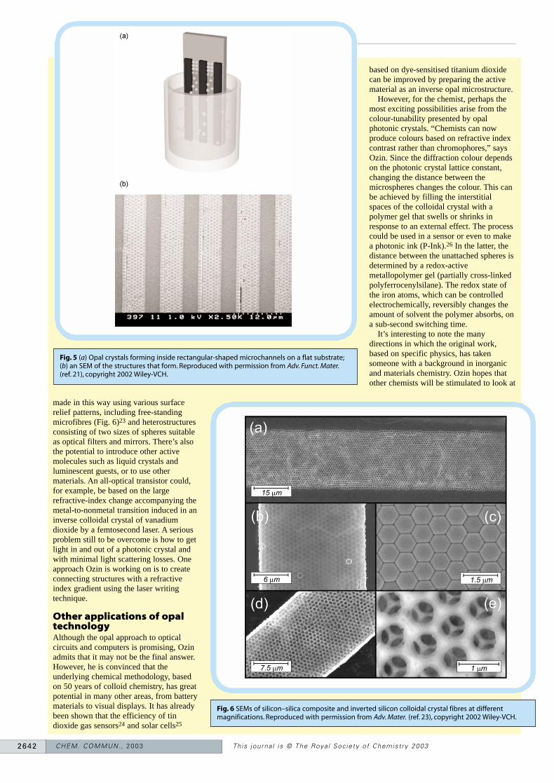
The next step has been to make well-defined photonic crystal shapes on orwithin a typical planar device like a siliconwafer, so as to create lasers, transistors,waveguides and other microoptical devicesthat could be integrated in an all-opticalchip. This was done by subtly combiningsoft lithography with colloidal crystal self-assembly. Ozin’s group fashioned V-shaped, rectangular and square channels ina silicon wafer and filled them with opalphotonic crystals (Fig. 5).21 A line-patterned master of polydimethylsiloxane(PDMS) was inked with an alkanethiol inethanol and printed onto a silicon wafercoated with gold and an adhesive layer oftitanium. The exposed gold surface and theunderlying silicon were sequentiallyetched away to form grooves. Silicamicrospheres dispersed in ethanol werethen coaxed by capillary forces into thetunnels by directed evaporation-inducedself-assembly or by placing a flat piece ofPDMS over the grooves. As the ethanolevaporated, the microspheres collectedinto lines with the desired fcc crystalstructure. Another approach that the teamhas worked on was to use spin-coating (thewafer is spun round while centrifugalforces spread the silica dispersion over it)to guide the spheres into sets of pre-formed channels or pits in the substrate.The pit dimensions can be designed so thatthey are commensurate with an integralnumber of spheres, resulting in well-defined ordering.22
A whole range of opal structures can be
2641This journa l is © The Roya l Soc iety of Chemistry 2003 CHEM. COMMUN., 2003
Fig. 3 Examples of binary colloidal crystal patterns and defects. Reproduced with permission fromAdv. Mater. (ref. 18), copyright 2003 Wiley-VCH.
Fig. 4 SEM images of the different steps in the MISO process (a) an inverse silica colloidal crystalmicro-mould; (b) an inverse silica-silicon composite colloidal crystal; (c,d) a silicon colloidal crystalwith novel topology. Reproduced with permission from Adv. Mater. (ref. 19), copyright 2003 Wiley-VCH.
made in this way using various surfacerelief patterns, including free-standingmicrofibres (Fig. 6)23 and heterostructuresconsisting of two sizes of spheres suitableas optical filters and mirrors. There’s alsothe potential to introduce other activemolecules such as liquid crystals andluminescent guests, or to use othermaterials. An all-optical transistor could,for example, be based on the largerefractive-index change accompanying themetal-to-nonmetal transition induced in aninverse colloidal crystal of vanadiumdioxide by a femtosecond laser. A seriousproblem still to be overcome is how to getlight in and out of a photonic crystal andwith minimal light scattering losses. Oneapproach Ozin is working on is to createconnecting structures with a refractiveindex gradient using the laser writingtechnique.
Other applications of opaltechnologyAlthough the opal approach to opticalcircuits and computers is promising, Ozinadmits that it may not be the final answer.However, he is convinced that theunderlying chemical methodology, basedon 50 years of colloid chemistry, has greatpotential in many other areas, from batterymaterials to visual displays. It has alreadybeen shown that the efficiency of tindioxide gas sensors24 and solar cells25
based on dye-sensitised titanium dioxidecan be improved by preparing the activematerial as an inverse opal microstructure.
However, for the chemist, perhaps themost exciting possibilities arise from thecolour-tunability presented by opalphotonic crystals. “Chemists can nowproduce colours based on refractive indexcontrast rather than chromophores,” saysOzin. Since the diffraction colour dependson the photonic crystal lattice constant,changing the distance between themicrospheres changes the colour. This canbe achieved by filling the interstitialspaces of the colloidal crystal with apolymer gel that swells or shrinks inresponse to an external effect. The processcould be used in a sensor or even to makea photonic ink (P-Ink).26 In the latter, thedistance between the unattached spheres isdetermined by a redox-activemetallopolymer gel (partially cross-linkedpolyferrocenylsilane). The redox state ofthe iron atoms, which can be controlledelectrochemically, reversibly changes theamount of solvent the polymer absorbs, ona sub-second switching time.
It’s interesting to note the manydirections in which the original work,based on specific physics, has takensomeone with a background in inorganicand materials chemistry. Ozin hopes thatother chemists will be stimulated to look at
CHEM. COMMUN., 2003 This journa l is © The Roya l Soc iety of Chemistry 20032642
Fig. 5 (a) Opal crystals forming inside rectangular-shaped microchannels on a flat substrate;(b) an SEM of the structures that form. Reproduced with permission from Adv. Funct. Mater.(ref. 21), copyright 2002 Wiley-VCH.
Fig. 6 SEMs of silicon–silica composite and inverted silicon colloidal crystal fibres at differentmagnifications. Reproduced with permission from Adv. Mater. (ref. 23), copyright 2002 Wiley-VCH.

this novel approach to chemicalmanipulation, whereby chemical form andphysical function are so happily married atthe nano and mesoscopic level.
AcknowledgementsNina Hall thanks Professor Ozin for hishelp with this article, and his coworkers,André Arsenault, Vladimir Kitaev, HernánMíguez, Nicolas Tétreault and San MingYang. Professor Ozin acknowledges thefinancial support for this work from theNatural Sciences and EngineeringResearch Council of Canada as well as theUniversity of Toronto.
Notes and references1 J. D. Joannopoulos, P. R. Villeneuve and S.
Fan, Nature (London), 1997, 386, 143.2 A. Blanco, E. Chomski, S. Grabtchak, M.
Ibisate, S. John, S. W. Leonard, C. Lopez,F. Meseguer, H. Míguez, J. P. Mondia, G.A. Ozin, O. Toader and H. M. van Driel,Nature (London), 2000, 405, 437.
3 S. Y. Lin and J. G. Fleming, IEEE J.Lightwave Technol., 1999, 17, 1944.
4 E. Yablonovitch, Phys. Rev. Lett., 1987, 58,
2059.5 S. John, Phys. Rev. Lett., 1987, 58, 2486.6 E. Yablonovitch, Sci. Am., December 2001,
35.7 P. Russell, Science (Washington D.C.),
2003, 299, 358.8 B. T. Holland, C. Blanford and A. Stein,
Science (Washington D.C.), 1998, 281,538.
9 J. E. G. J. Wijnhoven and W. L. Vos,Science (Washington D.C.), 1998, 281,802.
10 A. A. Zakhidov, R. H. Baughmann, Z.Iqbal, C. Cui, I. Khayrullin, S. O. Dantas,J. Marti and V. G. Ralchenko, Science(Washington D.C.), 1998, 282, 897.
11 R. C. Salvarezza, L. Vázquez, H. Míguez,R. Mayoral, C. López and F. Meseguer,Phys. Rev. Lett., 1996, 77, 4572.
12 H. Míguez, C. López, F. Meseguer, A.Blanco, L. Vázquez, R. Mayoral, M.Ocaña, V. Fornés and A. Mifsud, Appl.Phys. Lett., 1997, 71, 1148.
13 H. Míguez, F. Meseguer, C. López, A.Blanco, J. S. Moya, J. Requena, A. Mifsudand V. Fornés, Adv. Mater., 1998, 10, 483.
14 P. Jiang, J. F. Bertone, K. S. Hwang and V.L. Colvin, Chem. Mater., 1999, 11, 2132.
15 V. L. Colvin, MRS Bull., 2001, 26, 637.16 Y. A. Vlasov, X.-Z. Bo, J. C. Sturm and D.
J. Norris, Nature (London), 2001, 414,289.
17 H. Míguez, N. Tétreault, B. Hatton, S. M.Yang, D. Perovic and G. A. Ozin, Chem.Commun., 2002, 2736.
18 V. Kitaev and G. A. Ozin, Adv. Mater.,2003, 15, 75.
19 H. Míguez, N. Tétreault, S. M. Yang, V.Kitaev and G. A. Ozin, Adv. Mater., 2003,15, 597.
20 N. Tétreault, H. Míguez, V. Kitaev, S. M.Yang and G. A. Ozin, Adv. Mater., 2003,15, 1167.
21 S. M. Yang, H. Míguez and G. A. Ozin,Adv. Funct. Mater., 2002, 12, 425.
22 G. A. Ozin and S. M. Yang, Adv. Funct.Mater., 2001, 11, 95.
23 H. Mignez, S. M. Yang, N. Tetreault andG. A. Ozin, Adv. Mater., 2002, 14, 1805.
24 R. W. J. Scott, S. M. Yang, N. Coombs, G.A. Ozin and D. E. Williams, Adv. Mater,2001, 13, 1468.
25 S. Nishimura, N. Abrams, B. A. Lewis, L.I. Halaoui, T. E. Mallouk, K. D.Bekenstein, J. van de Lagemaat and A. J.Frank, J. Am. Chem. Soc., 2003, 125,6306.
26 A. C. Arsenault, H. Míguez, V. Kitaev, G.A. Ozin and I. Manners, Adv. Mater., 2003,15, 503.
2643This journa l is © The Roya l Soc iety of Chemistry 2003 CHEM. COMMUN., 2003