on-chip bus architecturevada.skku.ac.kr/.../comp-arch/soc-arch/%b8%f0%b5… · ·...
TRANSCRIPT
Module 10
On-Chip Bus Architecture
Module 10
On-Chip Bus Architecture
이론 3시간
이혁재
서울대학교

학습목표
• Shared on-chip bus의 중요성을 파악하고, 많이 사용되는shared bus 기반의 아키텍처를 소개한다.
• 하드웨어 모듈들 간에 동기화 (synchronization) 시키기 위한여러가지 방법을 이해한다.
• 여러 개의 하드웨어 모듈이 하나의 모듈을 공유하는 경우 버스를효율적으로 나누어서 사용할 수 있게 하는 arbitration 방법을이해한다.
• 많이 사용되고 있는 on-chip bus의 구조들의 장단점을 이해한다.
• 버스에서 전력 소모를 줄이는 방법을 이해한다.
• 자동으로 버스를 합성하고 최적화하는 방법을 이해한다.
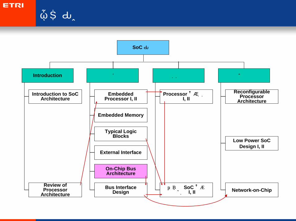
모듈구성
선택필수
SoC 구조
Embedded Processor I, II
Embedded Memory
Typical Logic Blocks
External Interface
On-Chip Bus Architecture
Bus Interface Design
실습
Processor 설계실습I, II
간단한 SoC 설계실습 I, II
Reconfigurable Processor
Architecture
Low Power SoC Design I, II
Network-on-Chip
Introduction
Introduction to SoC Architecture
Review of Processor
Architecture
강의자료활용 Guideline
• "1. Introduction"에서는 oh-chip bus의 기본적인 개념 및 많이사용되는 on-chip bus 구조를 소개한다.
• "2. Wire Delay and Synchronization"에서는 하드웨어컴포넌트들 사이에 통신 딜레이가 발생하는 경우 이를 극복하고통신을 수행할 수 있는 방법을 설명한다. 우선 delay가 작은경우부터 시작해서 설명을 하고, delay가 커지는 경우를해결하는 방법인 latency insensitive design의 개념 및 구현방법을 소개한다.
• "3. Arbitration"에서는 shared bus를 여러 개의 master가공유하는 경우 이들 사이에 우선 순위를 정하는 방법을 설명한다. 이 절에서는 간단한 방법부터 시작하여 좀더 복잡한 방법을설명한다.
• “4 Power Consumption”은 버스에서 power 소모를 줄이는방법을 소개한다.
• “5 Synthesis and Optimization”에서는 버스를 자동으로 합성할때에 최적화 기준 및 그 결과를 설명한다.
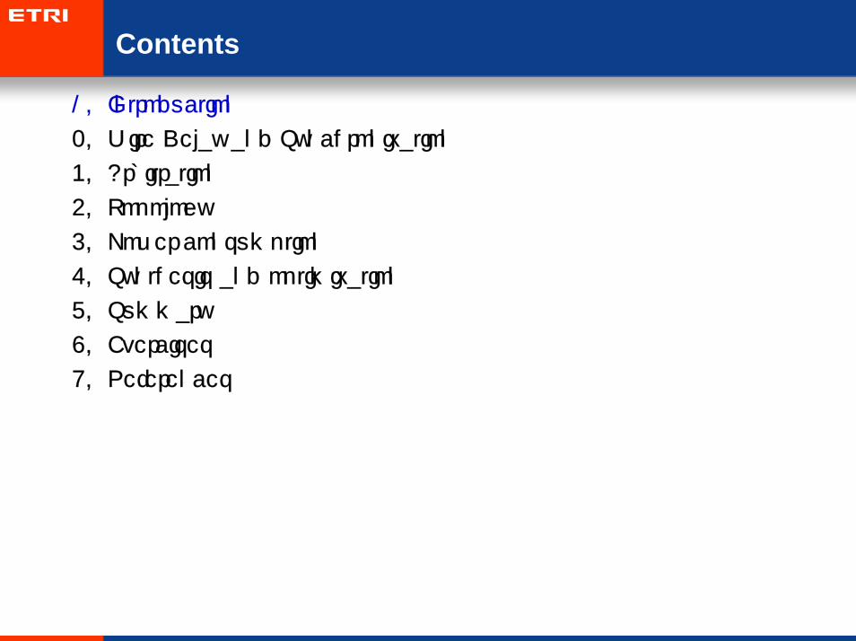
Contents
1. Introduction
2. Wire Delay and Synchronization
3. Arbitration
4. Topology
5. Power consumption
6. Synthesis and optimization
7. Summary
8. Exercises
9. References
On-Chip Bus (OCB) Architecture
CPU On-chipRAM
DMABus
Master
BRIDGE
UARTExternalMemoryInterface
Timer
PIOKeypad
High bandwidthbus
Low bandwidthbus
• Bus consists of address signals, data signals, and control signals
– Data signals: the data to be transmitted
– Address signals: the address at which data must be read from or written into
– Control signals: used for efficient transmission of data
• A bus is shared by many hardware components
– Only one bus master can use the bus
– Efficient for processor-centered system
On-Chip Bus (OCB) Architecture
• Example: AMBA AHB bus signals
slave
HADDR[31:0]HRDATA[31:0]HRESP[1:0]
master
HREADYHWRITEHWDATA[31:0]HTRANS[1:0]HBURST[2:0]HSIZE[2:0]
HCLK
On-Chip Bus (OCB) Architecture
• Example AMBA-based architecture: Leon processor architecture
On-Chip Bus (OCB) Architecture
• IBM CoreConnect Block Diagram
– DCR (Device Control Register) bus: data movement between CPU and registers
On-Chip Bus (OCB) Architecture
• Example CoreConnect-based architecture: PowerPC processor-based SoC
On-Chip Bus (OCB) Architecture
• DCR (Device Control Register) bus
– Very low bandwidth bus specially design for control registers access
– Maximum throughput: one read (or write) per every two cycles
– Implemented by distributed multiplexers
– Ring type connectivity: minimized bus area
Shared Bus Issues
• Long bus wire– Long communication time
• Slow operating clock
• Synchronization issue
– Large power consumption
– Crosstalk error prone
• Limited bandwidth– A single bus is shared by many hardware modules
– Starvation problem• Due to the priority-based bus arbitration, lower priority bus accesses can be
starved by frequent higher priority bus accesses.
• Real-time communication problem– Worst-case analysis is difficult.
• E.g. for the worst-case analysis, all the communications need to be modeled as real-time tasks.

Contents
1. Introduction
2. Wire Delay and Synchronization
3. Arbitration
4. Topology
5. Power consumption
6. Synthesis and optimization
7. Summary
8. Exercises
9. References
Conventional Bus: Basic Read Transaction
• Example: AMBA AHB
AHADDR[31:0]
HRESP[1:0]
HCLK
Data (A)HRDATA[31:0]
OK (A)
Address Phase Data Phase
Conventional Bus: Basic Read Transaction
• In the path from output of the master to the input to the master (represented by red arrows)
– Only a single register allowed from address to response/data
– Fast slave combinational logic required
Addrreg
resp/datareg
Combinationallogic
Combinationallogic
DeriveResponse And data
Derivethe nextaddress
master slave
Conventional Bus: WISHBONE
• Opencore standard interconnect architecture
• Single cycle data transfer
Conventional Bus: WISHBONE
• In the path from output of the master to the input to the master (represented by red arrows)
– No register allowed
– Even faster slave combinational logic required than AMBA
Addrreg
Combinationallogic
Combinationallogic
DeriveResponse And data
Derivethe nextaddress
master slave
Conventional Bus: Two Cycle Response
• If you want to insert two registers in the path allowed
– Slow combinational logic is possible
– Response/data requires two cycles
Addrreg
resp/datareg
Combinationallogic
Combinationallogic
Derivethe nextaddress
Conventional Bus: Two Cycle Response
• Wait state allows two (or more) cycle response
HADDR
HRESP
HCLK
A
Data (A)HRDATA
OK (A)
Slave Not Ready Slave Giving Data
Wait StateHREADY
Synchronization Issue
• By year of 2013– 32-nm technology available– Clock: 19-20 GHz.– Global wire delay: between 12 to 32 clock cycles
.
Latency-insensitive design
• Perl: synchronous components
• Shell: encapsulate each perl for delay insensitive communication
• Relay station: latches for long wires
• Channel: point-to-point unidirectional links.
• Back-pressure signal (the stop flag): indicates that the receiver hasits input buffer FULL.
• .
Latency-insensitive design: Relay Station
• DataIn, DataOut: data signals
• voidIn, voidOut: indication of valid data
• stopIn, stopOut: blocking data transmission
• In normal condition,
– use the main register
– dataOut(t+1) = dataIn(t)
• Data-out blocked
– If new data coming in,
– write the auxiliary register
• In stalling condition
– Data-out blocked twice
– No data input and output
- Stopin(t) stopOut(t+1)
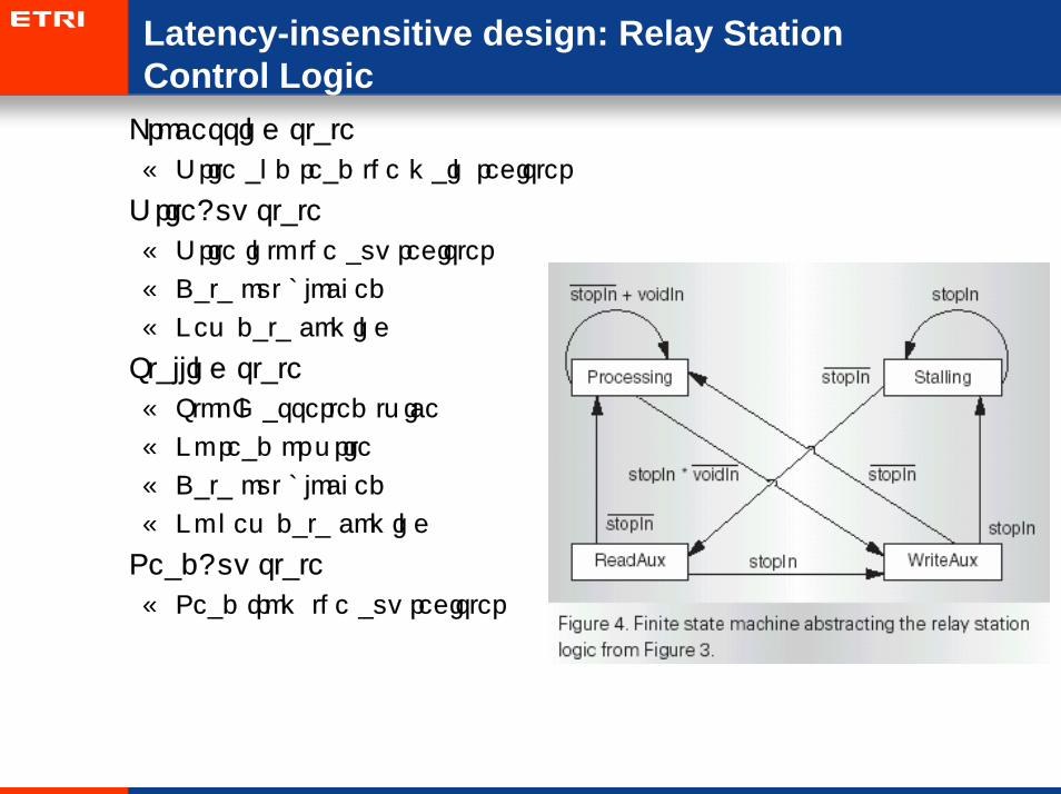
Latency-insensitive design: Relay Station Control Logic
• Processing state
– Write and read the main register
• WriteAux state
– Write into the aux register
– Data out blocked
– New data coming
• Stalling state
– StopIn asserted twice
– No read or write
– Data out blocked
– No new data coming
• ReadAux state
– Read from the aux register
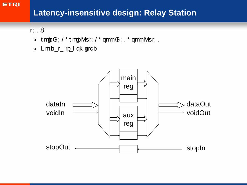
Latency-insensitive design: Relay Station
• t=0:
– voidIn=1, voidOut=1, stopIn=0, stopOut=0
– No data transmitted
mainreg
auxreg
dataIn dataOutvoidIn voidOut
stopOut stopIn
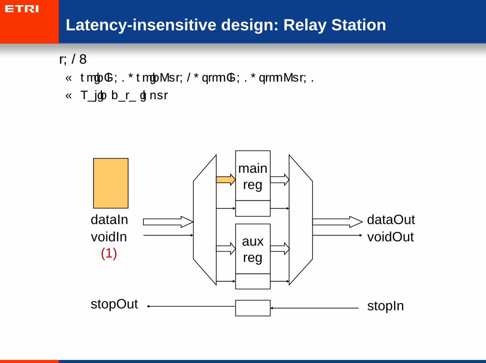
Latency-insensitive design: Relay Station
• t=1:
– voidIn=0, voidOut=1, stopIn=0, stopOut=0
– Valid data input
mainreg
auxreg
dataIn dataOutvoidIn
(1)voidOut
stopOut stopIn
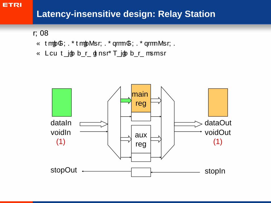
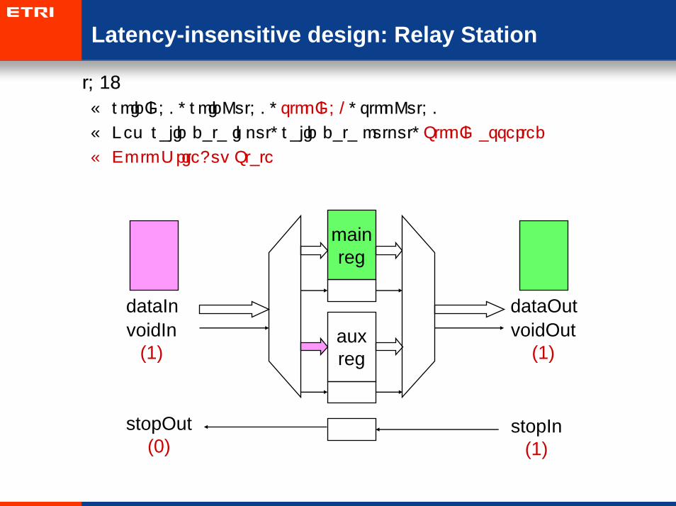
Latency-insensitive design: Relay Station
• t=2:
– voidIn=0, voidOut=0, stopIn=0, stopOut=0
– New valid data input, Valid data output
main reg
auxreg
dataIn dataOutvoidIn
(1)voidOut
(1)
stopOut stopIn

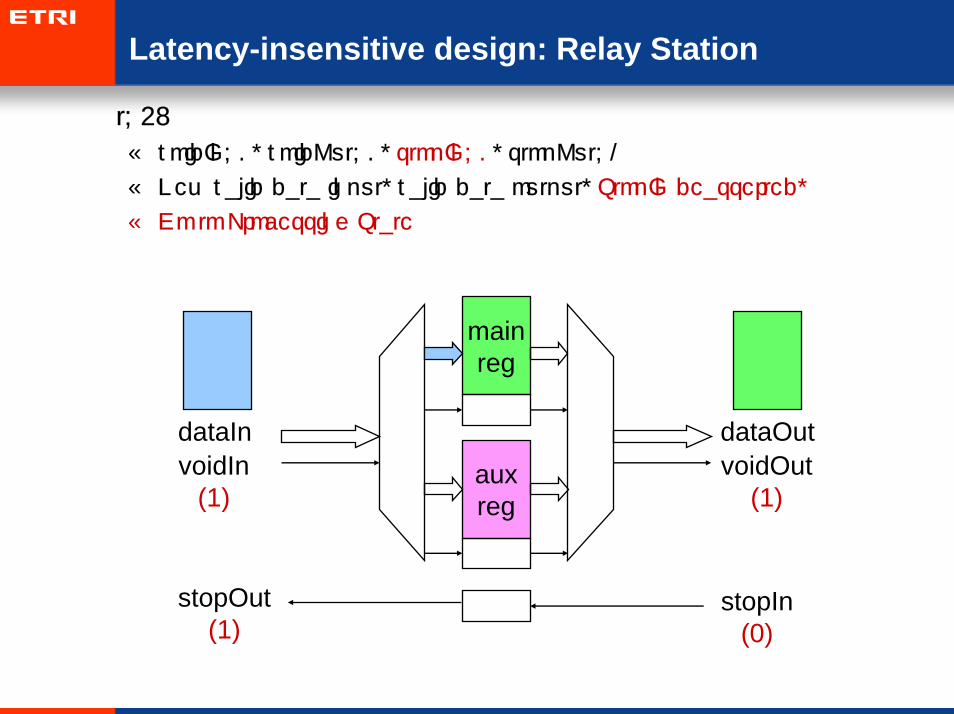
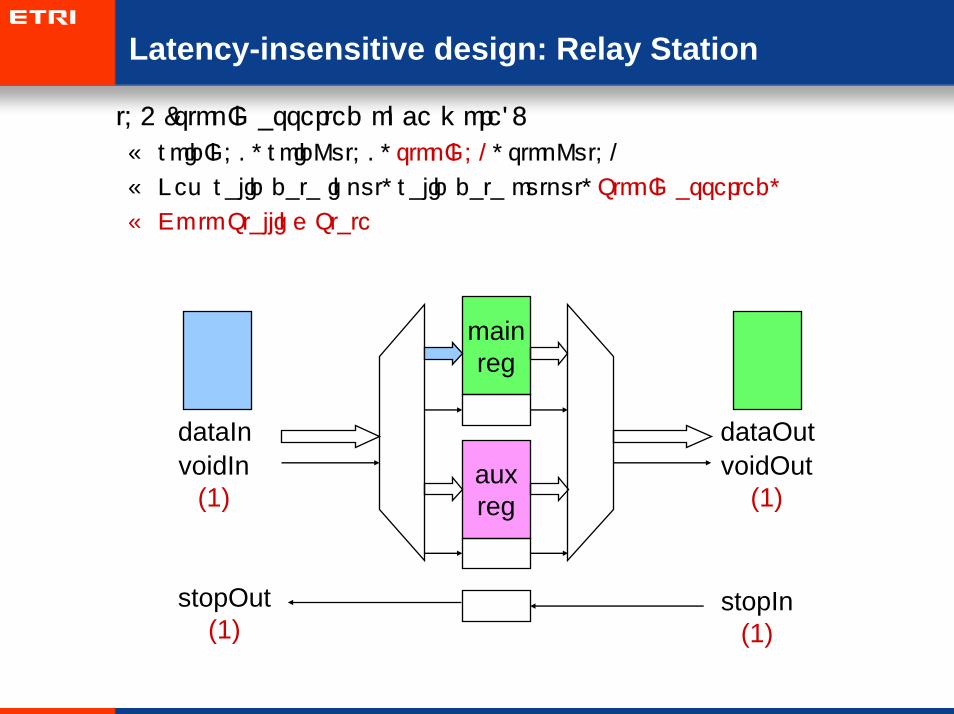
Latency-insensitive design: Relay Station
• t=3:
– voidIn=0, voidOut=0, stopIn=1, stopOut=0
– New valid data input, valid data output, StopIn asserted
– Go to WriteAux State
mainreg
auxreg
dataIn dataOutvoidIn
(1)voidOut
(1)
stopOut(0)
stopIn(1)
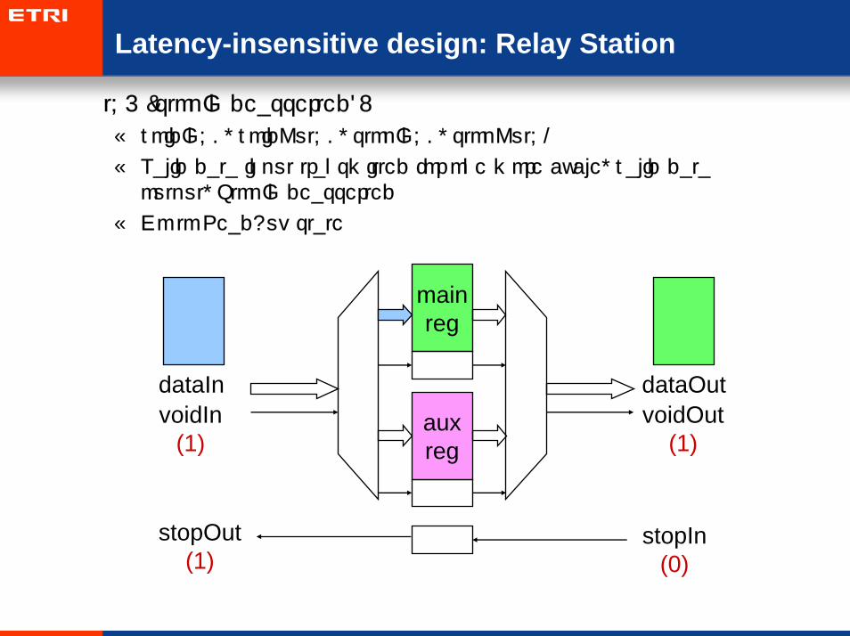
Latency-insensitive design: Relay Station
• t=4:
– voidIn=0, voidOut=0, stopIn=0, stopOut=1
– New valid data input, valid data output, StopIn deasserted,
– Go to Processing State
mainreg
auxreg
dataIn dataOutvoidIn
(1)voidOut
(1)
stopOut(1)
stopIn(0)
Latency-insensitive design: Relay Station
• t=5:
– voidIn=0, voidOut=0, stopIn=0, stopOut=0
– Valid data input transmitted for one more cycle, valid data output, StopIn deasserted,
mainreg
auxreg
dataIn dataOutvoidIn
(1)voidOut
(1)
stopOut(0)
stopIn(0)
Latency-insensitive design: Relay Station
• t=6:
– voidIn=0, voidOut=0, stopIn=0, stopOut=0
– Valid data input transmitted for one more cycle, valid data output, StopIn deasserted,
mainreg
auxreg
dataIn dataOutvoidIn
(1)voidOut
(1)
stopOut(0)
stopIn(0)
Latency-insensitive design: Relay Station
• t=3:
– voidIn=0, voidOut=0, stopIn=1, stopOut=0
– New valid data input, valid data output, StopIn asserted
– Go to WriteAux State
mainreg
auxreg
dataIn dataOutvoidIn
(1)voidOut
(1)
stopOut(0)
stopIn(1)
Latency-insensitive design: Relay Station
• t=4 (stopIn asserted once more):
– voidIn=0, voidOut=0, stopIn=1, stopOut=1
– New valid data input, valid data output, StopIn asserted,
– Go to Stalling State
mainreg
auxreg
dataIn dataOutvoidIn
(1)voidOut
(1)
stopOut(1)
stopIn(1)
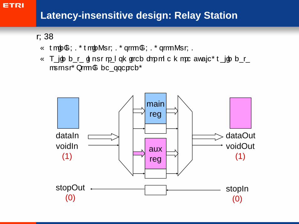
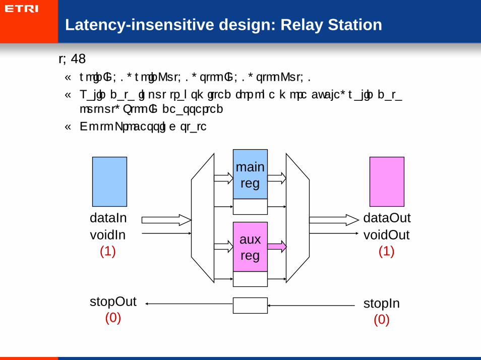
Latency-insensitive design: Relay Station
• t=5 (stopIn deasserted):
– voidIn=0, voidOut=0, stopIn=0, stopOut=1
– Valid data input transmitted for one more cycle, valid data output, StopIn deasserted
– Go to ReadAux state
mainreg
auxreg
dataIn dataOutvoidIn
(1)voidOut
(1)
stopOut(1)
stopIn(0)
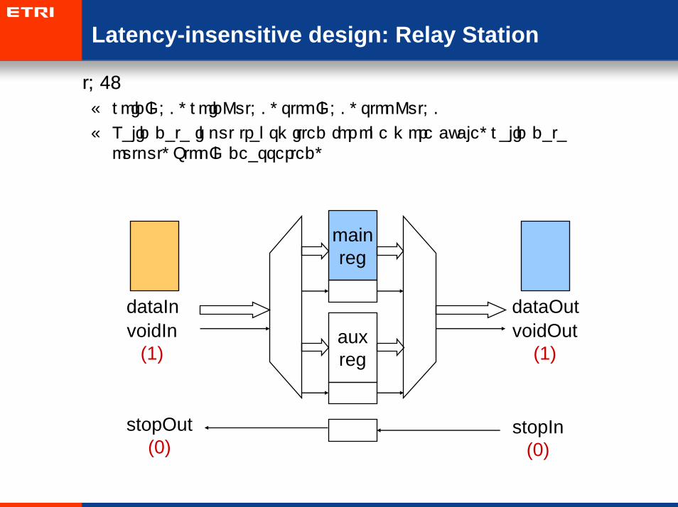
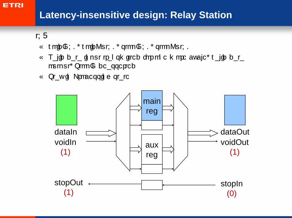
Latency-insensitive design: Relay Station
• t=6:
– voidIn=0, voidOut=0, stopIn=0, stopOut=0
– Valid data input transmitted for one more cycle, valid data output, StopIn deasserted
– Go to Processing state
mainreg
auxreg
dataIn dataOutvoidIn
(1)voidOut
(1)
stopOut(0)
stopIn(0)
Latency-insensitive design: Relay Station
• t=7
– voidIn=0, voidOut=0, stopIn=0, stopOut=0
– Valid data input transmitted for one more cycle, valid data output, StopIn deasserted
– Stay in Processing state
mainreg
auxreg
dataIn dataOutvoidIn
(1)voidOut
(1)
stopOut(1)
stopIn(0)
Latency-insensitive Design: Shell Encapsulation
Latency-insensitive design: AMBA 3.0 AXI
• New On-chip interconnect (AMBA 3.0 AXI) supports latency-insensitive design
• Channel architecture
– Four groups of signals
• Address “A” signal name prefix
• Read “R” signal name prefix
• Write “W” signal name prefix
• Write Response “B” signal name prefix
ADDRESS WRITE DATA
READ DATA RESPONSE
Latency-insensitive design: AMBA 3.0 AXI
• Channels - One way flow
– Each channel has information flowing in one direction only
– READY is the only return signal
– VALID: similar to void, READY: similar to stop
AVALIDADDRAWRITEALENASIZEABURSTALOCK
AIDAREADY
RVALIDRLASTRDATARRESPRIDRREADY
WVALIDWLASTWDATAWSTRBWIDWREADY
BVALIDBRESPBIDBREADY
APROTACACHE
Latency-insensitive design: AMBA 3.0 AXI
• Write burst
Latency-insensitive design: AMBA 3.0 AXI
• Example Register Slices
Master#1
Master#2
Slave#1
Slave#2
Slave#3
Slave#4
A
A
A
A
A
A
Master#1
Master#2
Slave#1
Slave#2
Slave#3
Slave#4
A
A
A
A
A
A
Master#1
Master#2
Slave#1
Slave#2
Slave#3
Slave#4
A
A
A
A
A
A
Isolate addresstiming
R
R
R
R
R
R
R
R
R
R
R
RIsolate poor
read data setupBreak long
interconnect path
AMBA AHB vs. AXI
• AMBA 2.0 AHB Burst
– AHB Burst
• Address and Data are locked together
• Single pipeline stage
• HREADY controls intervals of address and data
A21 A22 A23A11 A12 A13 A14
D21 D22 D23D11 D12 D13 D14
A31
D31
ADDRESS
DATA
AMBA AHB vs. AXI
• AXI - One Address for Burst
– AXI Burst
• One Address for entire burst
A21A11
D21 D22 D23D11 D12 D13 D14
A31
D31
ADDRESS
DATA
AMBA AHB vs. AXI
• AXI - Outstanding Transactions
– AXI Burst
• One Address for entire burst
• Allows multiple outstanding addresses
A21A11
D21 D22 D23D11 D12 D13 D14
A31
D31
ADDRESS
DATA
Latency-insensitive design: Error Handling
- Multiple outstanding transactions propagate across the link during the same clock cycle
- When transactions are correctly received at the destination switch, an ACK is propagated back to the source
- After N clock cycles, the transaction will be discarded from the buffer of the source
Latency-insensitive design: Error Handling
- After N clock cycles, the transaction will be discarded from the buffer of the source switch
- A corrupted transaction should be indicated by the destination and then source retransmits it again
Globally Asynchronous Locally Synchronous Network
• Asynchronous circuits
– Faster and less power consumption than synchronous circuits when designed properly.
– Widespread control overhead increasing die size
– More complex
– No CAD tool support
Synchronizer
Locallysynchronous
circuits
Locallysynchronous
circuits
Asynchronousprotocol
CLK1 CLK2
Globally Asynchronous Locally Synchronous Network
• Handling Asynchronous Inputs
D Q
D Q
Q0
Clock
Clock
Q1
AsyncInput
Clocked Synchronous
System
D Q
D Q
Q0
Clock
Clock
Q1
AsyncInput D Q
Synchronizer
Never allow asynchronous inputs to be fanned out to more than Never allow asynchronous inputs to be fanned out to more than one FF within the synchronous systemone FF within the synchronous system
Globally Asynchronous Locally Synchronous Network
• What Can Go Wrong
In is asynchronousIn is asynchronousFans out to D0 and D1Fans out to D0 and D1
One FF catches theOne FF catches thesignal, one does notsignal, one does not
impossible state mightimpossible state mightbe reached!be reached!
Setup time violation!Setup time violation!In
Q 0
Q 1
Clk
Single FF that receives the asynchronous signal is Single FF that receives the asynchronous signal is a synchronizera synchronizer
Globally Asynchronous Locally Synchronous Network
• Solutions to Synchronizer Failure
– use fastest possible logic in the synchronizer
• this makes for a very sharp "peak" upon which to balance
• S or AS TTL D-FFs are recommended
– cascade two synchronizers
DD DDQQ QQ
ClkClk
AsynchronousAsynchronousInputInput
SynchronizedSynchronizedInputInput
Synchronous SystemSynchronous System
Asynchronous Wrapper with Pausable Clock
• Asynchronous wrapper
• On the arrival of data, the clock at the wrapper is stopped no synchronization problem takes place
Asynchrounous wrapper
Locallysynchronous
circuits
Locallysynchronous
circuits
Asynchronousprotocol
CLK1 CLK2
FIFO Interface
• FIFO is a common interface between different clock domain
• As long as FIFO is not empty or full, FIFO can de-couple the input domain and the output domain
• Useful for transmitting streaming data
sender receiver
• Wrapper connecting different clock domains• Easy to design an wrapper when one clock frequency is a
multiple of the other clock frequency• Treat long communication delay as a slow clock domain
Locallysynchronous
circuits
Locallysynchronous
circuits
synchronousprotocol
(slow domain)
CLK
Wrapper
Fully Synchronous Communication w/ Support of Multiple Clock Operations

Contents
1. Introduction
2. Wire Delay and Synchronization
3. Arbitration
4. Topology
5. Power consumption
6. Synthesis and optimization
7. Summary
8. Exercises
9. References
Static Priority Based Shared Bus
• The bus arbiter grants bus access to the master of highest priority
• No control over the fraction of communication bandwidth assigned to each component causes starvation
• The lowest priority component uses about 0.4% of bandwidth
TDMA Based Shared Bus
• TDMA: Time Division Multiplexed Access
• First level:
– Timing wheel has slots reserved for unique components.
– If the master associated with the current slot has an pending request, a single word transfer is granted, and the wheel is rotated by one slot.
– Masters can be prioritized by assigning different number of slots to different masters.
• Second level: if the current slot does not have a pending request,
– gives grant the next request
in a round-robin fashion.
TDMA Based Shared Bus
• Advantages
– Communication bandwidth guarantee
• E.g. Guaranteed BW: A: 40%, B:25%, C:35%
– Simple analysis of worst case bus access delay
• E.g. Worst case bus access delay of module A = 18 (time units)
2010 30 40 Time0A
BC
AB
C
50
Worst case bus access delayof module A is 18 (time units).
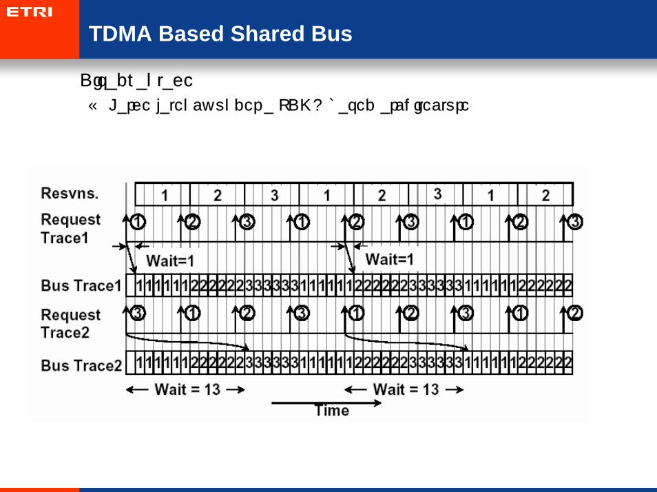
TDMA Based Shared Bus
• Disadvantage
– Large latency under a TDMA based architecture
Lotterybus
• Goal
– Fine-grained control over the fraction of bandwidth
– Fast execution (low latency) for high priority communications
• Lottery ticket: number of tickets assigned to each master depending on its priority.
• Lottery manager: probabilistically choose the winner with the tickets
Lotterybus
Lotterybus: Bandwidth Utilization
• High bus utilization (T4, T5, T7, T8, T9)
– allocated bandwidth = assigned tickets
– 1.15 : 2.09 : 2.96 : 3.83 = 1 : 2 : 3 : 4
• Low bus utilization (T3, T6)
– allocated bandwidth = 1 : 1 : 1 : 1
Lotterybus: Latency
• The latency for high priority master varies significantly in TDMA.

Contents
1. Introduction
2. Wire Delay and Synchronization
3. Arbitration
4. Topology
5. Power consumption
6. Synthesis and optimization
7. Summary
8. Exercises
9. References
Split Bus
• A solution to the performance degradation by excessive bus conflict Split bus
• Optimization issue1: Split or Not ?– The more modules in a bus, the slower the bus clock Split is better
• Due to the capacitive load of bus drivers
– Bus bridge overhead slow communication across bus Do not split
• Optimization issue2: Which modules connected to the same bus ?
– Place frequently communicating modules closer
– Bus topology and module mapping problems
A B C D
A B C D
Br
A D B C
Br
shared bus
Which one gives better performance?
Too much conflict!
Split Bus Architecture
• Bus interconnection with bridges
SRAM IP SRAM
bridge
bridgeSRAM IP SRAM
bridge
bridgeSRAM IP SRAM
bridge
bridgeSRAM IP SRAM
bridge
bridge
Split Bus Architecture
• Arbiter and switch select global bus connection
IP Decoder/arbiter SRAM
IP Decoder/arbiter SRAM
IP Decoder/arbiter SRAM
IP Decoder/arbiter SRAM
Arbiter &Switch
Global bus
Split Bus Architecture
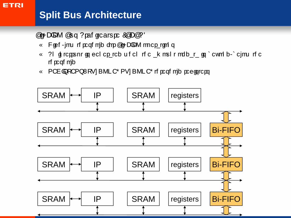
• Bi-FIFO Bus Architecture (BFBA)
– High/low threshold for Bi-FIFO operations
– An interrupt is generated when the amount of data is beyond/below the threshold
– REGISTERS: TX_DONE, RX_DONE, threshold registers
SRAM IP SRAM
SRAM IP SRAM
SRAM IP SRAM
SRAM IP SRAM
registers
registers
registers
registers
Bi-FIFO
Bi-FIFO
Bi-FIFO
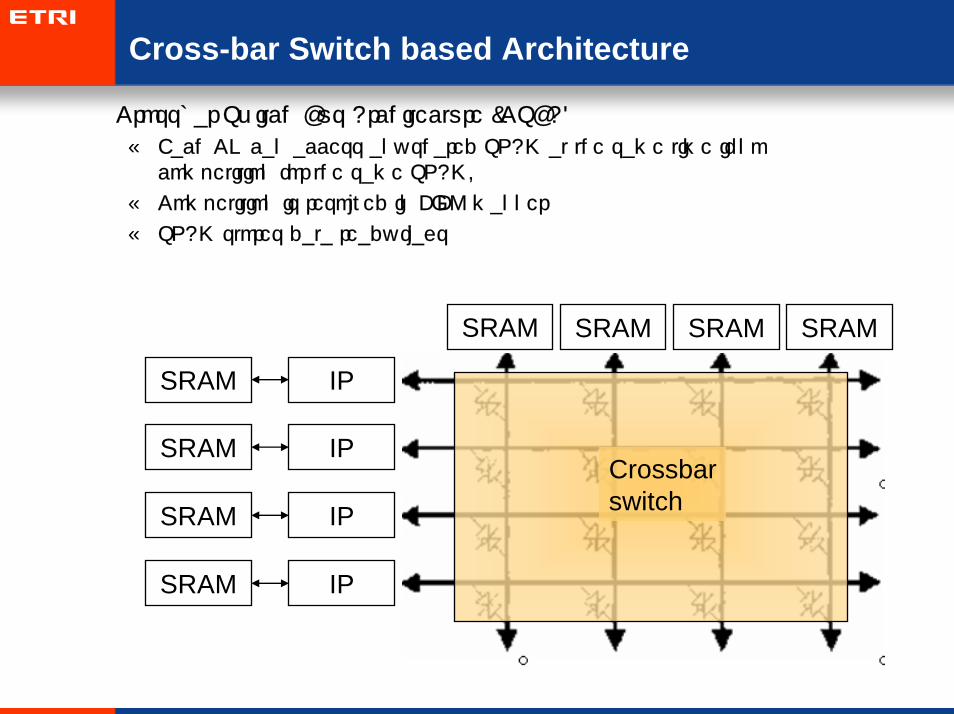
Cross-bar Switch based Architecture
• Crossbar Switch Bus Architecture (CSBA)
– Each CN can access any shared SRAM at the same time if no competition for the same SRAM.
– Competition is resolved in FIFO manner
– SRAM stores data ready flags
SRAM IP
SRAM
SRAM IP
SRAM
SRAM IP
SRAM
SRAM IP
SRAM
Crossbarswitch
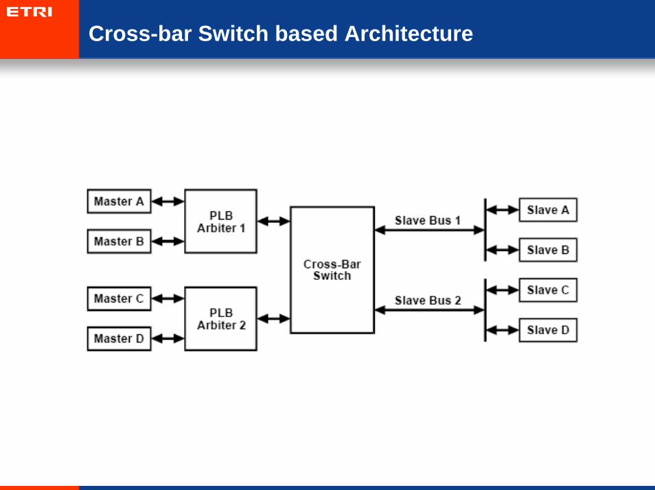
Cross-bar Switch based Architecture
Multimedia SoC Architecture
• Phillips DTV Chip: PROPHID Architecture
For high throughput: ~ 40 Gbps(Circuit switch network, 20 proc’s, 64MHz)
CPU
I$ D$
Circuit switch network
arb memADSProc
ADSProc
ADSProc
ADSProc
Programmabilityand control app’s
Control-oriented busApplication-specific processordata-driven execution
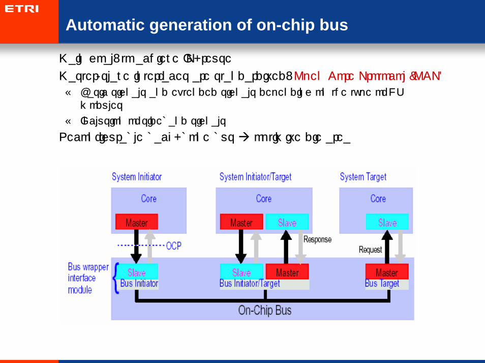
Automatic generation of on-chip bus
• Main goal: to achieve IP-reuse
• Master/slave interfaces are standardized: Open Core Protocol (OCP)
– Basic signals and extended signals depending on the type of HW modules
– Inclusion of sideband signals
• Reconfigurable back-bone bus optimize die area
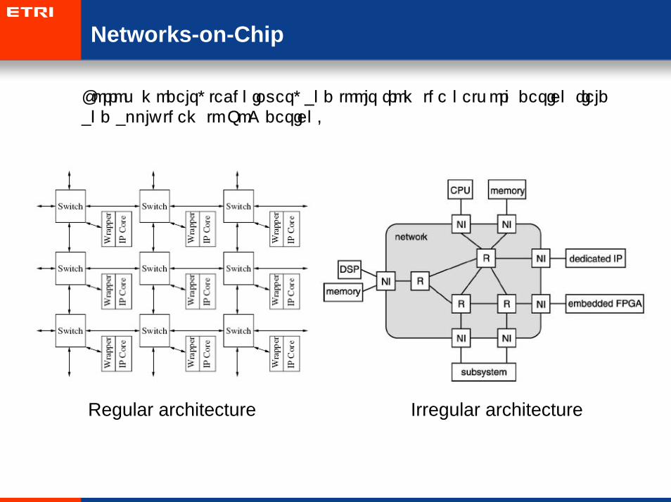
Networks-on-Chip
• Borrow models, techniques, and tools from the network design field and apply them to SoC design.
Regular architecture Irregular architecture
Networks-on-Chip
• Layered Protocol Architecture
– Packetization (transport layer)
• Data are decomposed into several data chucks.
– Due to the available maximum packet size
– Flow and congestion control (transport layer)
• Acknowledge message-based
• Error rate-based
– Routing is done by the routers (network layer)
– Error control (transport and/or data link layer)
• Retransmission: Go back N, SRP, etc.
• Error correction
• Link-by-link: data link layer
• End-to-end: transport layer
Software
application
system
Architecture & control
transport
network
data link
Physical
wiring
Interconnection Topology
Linear Ring
Mesh Torus
HWmodule
Folded Torus
• Point-to-point interconnection
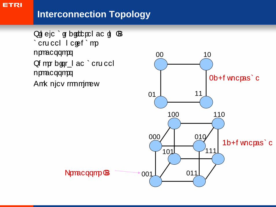
Interconnection Topology
• Single bit difference in ID between neighbor processors
• Short distance between processors
• Complex topology
00 10
01 11
2d-hypercube
100 110
101 111
000 010
001 011
3d-hypercube
Processor ID
Interconnection Topology
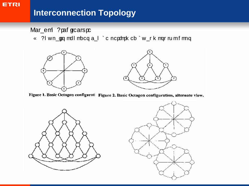
• Octagon Architecture
– Any pairs of nodes can be performed by at most two hops
• .
Interconnection Topology
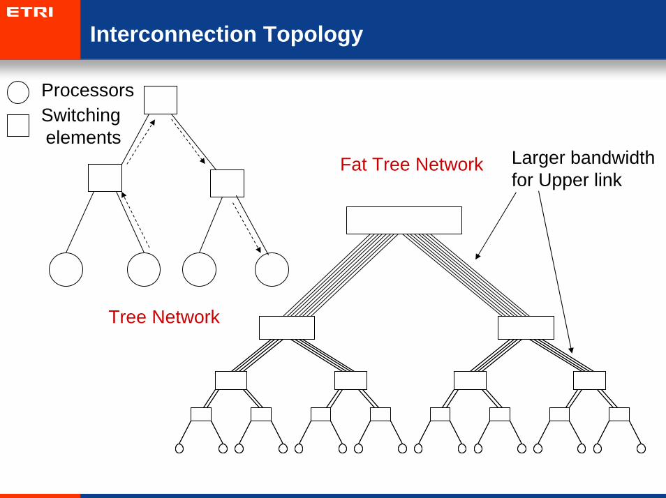
ProcessorsSwitching elements
Larger bandwidth for Upper link
Tree Network
Fat Tree Network
Interconnection Topology
• .
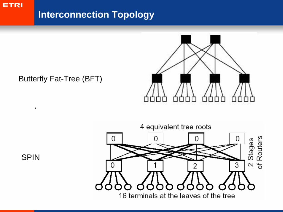
Butterfly Fat-Tree (BFT)
SPIN
Interconnection Topology
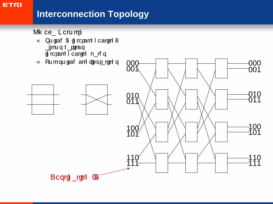
• Omega Network– Switch & interconnection:
allows various interconnection paths
– Two switch configurations 000001
111110
010
100
011
101
000001
010011
100101
110111
Destination ID
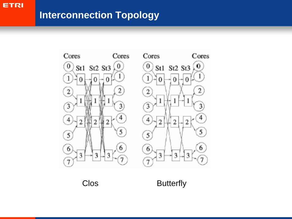
Interconnection Topology
Clos Butterfly
Contents
1. Introduction
2. Wire Delay and Synchronization
3. Arbitration
4. Topology
5. Power consumption
6. Synthesis and optimization
7. Summary
8. Exercises
9. References
Power Reduction by Bus Encoding
• Importance of low power design:
– SOC increasing number of transistors in a single chip
increasing power consumption
– Portable device battery lifetime not long enough
• Bus encoding for power reduction:
– reduce switching activities
– Possibly without additional control signals
• Idea: minor data change in sequential bus accesses
Master Master
encoder
decoder
Slave Slave
Power Reduction by Bus Encoding
• Bus-Invert method
– Let N be the number of bus bits
– If the hamming distance of consecutive data is greater than N/2,then invert the data
– 1-bit line added to represent the inversion
– Example)
• Source Encoded word inversion bit
0001 0001 0
0010 0010 0
0101 0010 1
– Good for random pattern (i.e., data bus)
Power Reduction by Bus Encoding
• T0 code
– Add 1-bit line, INC
– If the consecutive data just increment their values, the sender freezes the value on the bus and sets the INC line
– Otherwise, INC is de-asserted and the original data is sent
– Example)
• Source Encoded word INC
0001 0001 0
0010 0001 1
0101 0101 0
– Average of 60% reduction in bus switching activity
• Codebook method
– Given data, find the corresponding codeword in the codebook and send the codeword.
– Receiver also contains the codebook for decoding
Power Reduction by Bus Encoding
• Terminology for complex encodings– b(t) : source data at time t– B(b) : encoded codeword at time t– S: stride, i.e. the difference between consecutive source word
• T0-C code– No redundant line– If b(t) and b(t-1) are incremental difference, simply send b(t-1)– Otherwise, send the original address
– Exampleb(t) 39 40 41 44B(t) 39 39 39 44
– The only failure case• The backward branch target address is the same as the current (frozen) bus
value– Example
b(t) 39 40 41 39B(t) 39 39 39 ?
• Send b(t-1) + S – Note if b(t) = b(t-1) + S, then b(t-1) will be sent. – In the above example, send 40
– Reduction: 14% more than T0 code
Power Reduction by Bus Encoding
• T0-Xor
• B(t) = b(t) xor (b(t-1) + S) xor B(t-1)
– If consecutive source data simply increment, no switching activity occurs
– Example) S=1
• Source b(t) xor b(t-1)+S Encoded word
100001 - 100001
100010 000000 100001
100101 000111 100110
• Offset-Xor
– B(t) = (b(t) – b(t-1) ) xor B(t-1)
• Offset-Xor-S code
– B(t) = (b(t) – b(t-1) -S) xor B(t-1)
Power Reduction by Bus Encoding
• Offset-Xor-SM – B(t) = LSBINV((b(t) – b(t-1) -S) xor B(t-1)
– LSBINV (): invert all bits except the most significant bit (MSB) if the input is negative (i.e., the MSB is ‘1’)
– Example)
original offset FFFFFFFF (-1) FFFFFFFE (-2) 80000000
Modified offset
– More than 40% improvement over Offset-Xor
• Codebook: converts K bits to another K bits– To reduce the number of ‘1’s, the smaller numbers map to the numbers
with fewer number of ‘1’s
– If (x1 < x2) then NumOnes (CB(x1)) <= NumOnes (CB(x2))• For example
– CB(0000) 0000, CB(0001) 0001, CB(0010) 0010, CB(0011) 0100, CB(0100) 0011,…
– NumOnes(0011) > NumOnes(0100)
– NumOnes(CB(0011)) < NumOnes(CB(0100)
– B(t) = CB(LSBINV((b(t) – b(t-1) -S)) xor B(t-1)
– 4% saving compared to Offset-Xor-SM
Power Reduction by Bus Encoding
• Consecutive source word Xor problem:
– Even though the distance of b(t) and b(t-1)+S is small,
– XOR results in a large number of ‘1’s
– Eg) 61 68
• Source b(t) xor b(t-1)+S Encoded word
0111101 (61) - 0111101
1001000 (68) 1110101 1001000
– Small negative offset problem: large number of ‘1’s in b(t)-b(t-1)
– This problem occurs more frequently in real programs.
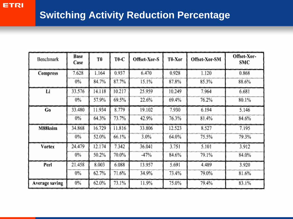
Switching Activity Reduction Percentage

Contents
1. Introduction
2. Wire Delay and Synchronization
3. Arbitration
4. Topology
5. Power consumption
6. Synthesis and optimization
7. Summary
8. Exercises
9. References
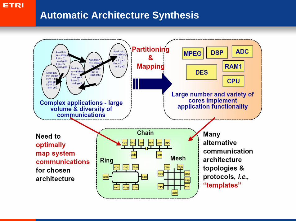
Automatic Architecture Synthesis
Automatic Bus Split
• Example system of communicating components
– Ci: component executing communication
– Bold line: data transfer
– Dotted line: control or synchronization signals
Automatic Bus Split
• Transactions spanning multiple buses to be minimized
• Components exchanging large amounts of data to be attached at the same bus
• Overlapped communications to be separated to different buses
Automatic Bus Split
• Effect of bus protocol
– Priority change
– DMA size: the maximum block transfer size
Power Consumption Optimization
• Power consideration– The fewer modules on a bus segment, the lower power consumption on
the shared bus.
– A split bus consumes lower power than a single bus.
• An optimization problem– Obtain bus topology and module mapping
– To minimize comm. delay while reducing bus power consumption.
A B C D A B C D
BrCbus 0.5Cbus 0.5Cbus
>
Power Consumption Optimization: Split-bus
• Average energy consumption
– Monolithic bus architecture: E1 = 0.5 sw CBUS Vdd2
• sw: average switching activity
– Split-bus architecture
E2 = 0.5 sw Vdd2 [ CBUS1 ∑i∈BUS1 ∑j∈BUS1,i ≠ j xfer(Mi,Mj)
+ CBUS2 ∑i∈BUS2 ∑j∈BUS2,i ≠ j xfer(Mi,Mj)
+ (CBUS1 + CBUS2) ∑i∈BUS1 ∑j∈BUS2, xfer(Mi,Mj)]
- CBUS1 ,CBUS2 : physical capacitance on bus1 and bus2
- xfer(Mi, Mj): the probability of data transfer from module Mi to Mj
• Assumption
– sw = 0.5
– CBUS1 /|BUS1| = CBUS2 /|BUS2| = CBUS /n = 1
– Vdd=1
Power Consumption Optimization: Split-bus
• Example 1: n = 2k, |BUS1| = k –a, |BUS2| = k + a
– xfer(Mi, Mj) = 1/(2k (2k-1))
– E1 = 0.5k
– E2 = 0.25 (3k3 - k2 + a2 (k - 1))/(2k2 – k)
– Energy saving of the split bus:
• (E1-E2)/E1 = 0.5 (k3 - k2 - a2 (k - 1))/(2k3 – k2)
• Maximized when a = 0
• k=2, a=0 16% energy saving
• K ∞, a=0 25% energy saving
• a=k energy saving = 0
Power Consumption Optimization: Split-bus
• Example 2: assume 4 modules connected to the bus
– x(Mi, Mj): probability of data exchange between module Mi and Mj
– x(Mi, Mj) = xfer(Mi, Mj) + xfer(Mj, Mi)
Power Consumption Optimization: Split-bus
• Example 3: assume 5 modules connected to the bus

Contents
1. Introduction
2. Wire Delay and Synchronization
3. Arbitration
4. Topology
5. Power consumption
6. Synthesis and optimization
7. Summary
8. Exercises
9. References

4. Summary
• On-chip bus는 address, data 및 control signal들로 구성된다.
• 현재 popular bus architecture는 a single high-bandwidth a single low-bandwidth bus이지만, 제한된 bandwidth, synchronization, 및 높은 power consumption등의 이슈가 있다.
• 칩의 동작 주파수에 최적화 되도록 communication protocol이정해진다.
• 칩 내부에서 communication도 여러 싸이클이 걸리게 되며 이에따라서 멀리 떨어진 IP들 간에 synchronous 통신을 위해서 IP들사이에 relay station을 둔다. 또다른 방법으로서는 GALS, FIFO, Wrapper 사용등이 존재한다.
• 하나의 버스를 여러 개의 master가 공유하는 경우 arbitration이필요한데, low priority master가 starvation하지 않으면서도 high priority master의 버스 접근 시간을 보장해 주어야 한다.
• 제한된 bandwidth를 해결하기 위하여 bus를 split하거나, 다양한topology의 one-to-one connection을 사용할 수 있다.
• 버스를 split하는 경우 각 IP들간의 communication 특성을고려하면, split 이후의 성능 및 전력 소모를 최적화 시킬 수 있다.
Contents
1. Introduction
2. Wire Delay and Synchronization
3. Arbitration
4. Topology
5. Power consumption
6. Synthesis and optimization
7. Summary
8. Exercises
9. References
5. Exercises
1. Shared on-chip bus를 사용하는 경우 발생할 수 있는문제점들을 설명하고, 이러한 문제점들을 해결할 수 있는 방법을제시하시오.
2. Synchronization 문제를 해결할 수 있는 여러가지 방법들을설명하고 이들 방법들의 장단점을 비교하시오.
3. Shared bus를 arbitration하는 방법들을 설명하고, 그장단점들을 비교하시오.
4. 버스에서 데이터 전송시에 발생하는 전력소모를 줄이기 위한방법을 설명하시오.
5. 하나의 shared bus를 사용하는 경우와 이를 2개의 bus로분리하는 경우 어떠한 하드웨어 모듈들끼리 같은 bus에연결되어야 하는가 ? 그 이유를 설명하시오.

Contents
1. Introduction
2. Wire Delay and Synchronization
3. Arbitration
4. Topology
5. Power consumption
6. Synthesis and optimization
7. Summary
8. Exercises
9. References
6. References
• [1] L. P. Carloni, A. L. Sangiovanni-Vincentelli, “Coping with Latency In SoC Design,” IEEE Micro, 2002.
• [2] T. Chelcea and S. Nowick, “A Low-Latency FIFO for Mixed-Clock Systems,” Computer Science Workshop on VLSI, 2002.
• [3] Jens Muttersbach, Thomas Villiger, and Wolfgan Fichtner, “Practical Design of Globally Asynchronous Locally Synchronous Systems,” International Symposium on Asynchronous Circuits and Systems, 2000.
• [4] K. Lahiri, A. Raghunathan, G. Lakshminarayana, “LOTTERYBUS: A New High-Performance Communication Architecture for System-on-Chip Designs,” DAC 2001.
• [5] K. Ryu, E. Shin, and V. Mooney, “A Comparison of Five Different Multiprocessor SoC Bus Architecture,” 2001.
• [6] Luca Benini, Giovanni De Micheli, “Networks on Chips: A New SoC Paradigm,” IEEE Computer, 2002.
• [7] Y. Aghaghiri, et. al., “Irredundant Address Bus Encoding for Low Power,” ISLPED 2001.
• [8] K. Lahiri, A. Raghunathan, S. Dey, “Efficient Exploration of the SoC Communication Architecture Design Space,” ICCAD 2000.
• [9] C. Hsieh and M. Pedram, “Architectural Energy Optimization by Bus Splitting,” IEEE Trans. CAD, 2002.