on-chip peripheral bus - columbia universitysedwards/classes/2005/emsys-summer/opb_ibm...advanced...
TRANSCRIPT
On-Chip Peripheral Bus
Architecture Specifications
Version 2.1
SA-14-2528-02

Advanced Information (April 2001)
This edition of On-chip Peripheral Bus Architecture Specifications applies to the IBM OPB Bus, until otherwise indicated in new versions or application notes.
The following paragraph does not apply to the United Kingdom or any country where such provisions are inconsistent with local law: INTERNATIONAL BUSINESS MACHINES CORPORATION PROVIDES THIS MANUAL “AS IS” WITHOUT WARRANTY OF ANY KIND, EITHER EXPRESSED OR IMPLIED, INCLUDING, BUT NOT LIMITED TO, THE IMPLIED WARRANTIES OF MERCHANTABILITY AND FITNESS FOR A PARTICULAR PURPOSE. Some states do not allow disclaimer of express or implied warranties in certain transactions; therefore, this statement may not apply to you.
IBM does not warrant that the products in this publication, whether individually or as one or more groups, will meet your requirements or that the publication or the accompanying product descriptions are error-free.
This publication could contain technical inaccuracies or typographical errors. Changes are periodically made to the information herein; these changes will be incorporated in new editions of the publication. IBM may make improvements and/or changes in the product(s) and/or program(s) described in this publication at any time.
It is possible that this publication may contain references to, or information about, IBM products (machines and programs), programming, or services that are not announced in your country. Such references or information must not be construed to mean that IBM intends to announce such IBM products, programming, or services in your country. Any reference to an IBM licensed program in this publication is not intended to state or imply that you can use only IBM’s licensed program. You can use any functionally equivalent program instead.
No part of this publication may be reproduced or distributed in any form or by any means, or stored in a data base or retrieval system, without the written permission of IBM.
Requests for copies of this publication and for technical information about IBM products should be made to your IBM Authorized Dealer or your IBM Marketing Representative.
Address comments about this publication to:
IBM CorporationDepartment YM5AP.O. Box 12195Research Triangle Park, NC 27709
IBM may use or distribute whatever information you supply in any way it believes appropriate without incurring any obligation to you.
Copyright International Business Machines Corporation 1996 - 2001. All rights reserved
4 3 2 1
Notice to U.S. Government Users – Documentation Related to Restricted Rights – Use, duplication, or disclosure is subject to restrictions set forth in GSA ADP Schedule Contract with IBM Corporation.

Patents and Trademarks
IBM may have patents or pending patent applications covering the subject matter in this publication. The furnishing of this publication does not give you any license to these patents. You can send license inquiries, in writing, to the IBM Director of Licensing, IBM Corporation, 208 Harbor Drive, Stamford, CT 06904, United States of America.
The following terms are trademarks of IBM Corporation:
IBMCoreConnectOther terms which are trademarks are the property of their respective owners.


Contents
Figures . . . . . . . . . . . . . . . . . . . . . . . . . . . . . . . . . . . . . . . . . . . . . . . . . . . . . . . . . . . . . . . . 9Tables. . . . . . . . . . . . . . . . . . . . . . . . . . . . . . . . . . . . . . . . . . . . . . . . . . . . . . . . . . . . . . . . 11About This Book . . . . . . . . . . . . . . . . . . . . . . . . . . . . . . . . . . . . . . . . . . . . . . . . . . . . . . . 13
Chapter 1. OPB Overview . . . . . . . . . . . . . . . . . . . . . . . . . . . . . . . . . . . . . . . . . . . . . . . . 1Physical Implementation . . . . . . . . . . . . . . . . . . . . . . . . . . . . . . . . . . . . . . . . . . . . . . . . . . . . . . . 3
Chapter 2. OPB Signals . . . . . . . . . . . . . . . . . . . . . . . . . . . . . . . . . . . . . . . . . . . . . . . . . . 6Signal Naming Conventions . . . . . . . . . . . . . . . . . . . . . . . . . . . . . . . . . . . . . . . . . . . . . . . . . . . . 6
Arbitration Signals . . . . . . . . . . . . . . . . . . . . . . . . . . . . . . . . . . . . . . . . . . . . . . . . . . . . . . . . . . . . 8Mn_request (Master Bus Request) . . . . . . . . . . . . . . . . . . . . . . . . . . . . . . . . . . . . . . . . . . . . . 8OPB_pendReqn (OPB Pending Master Request) . . . . . . . . . . . . . . . . . . . . . . . . . . . . . . . . . . 9OPB_busLock, Mn_busLock(OPB Bus Arbitration Lock) . . . . . . . . . . . . . . . . . . . . . . . . . . . . 9OPB_MnGrant (OPB Master Bus Grant) . . . . . . . . . . . . . . . . . . . . . . . . . . . . . . . . . . . . . . . . . 9OPB_timeout (OPB Timeout Error) . . . . . . . . . . . . . . . . . . . . . . . . . . . . . . . . . . . . . . . . . . . . 10OPB_retry, Sln_retry(OPB Bus Cycle Retry) . . . . . . . . . . . . . . . . . . . . . . . . . . . . . . . . . . . . . 10
Bus Signals . . . . . . . . . . . . . . . . . . . . . . . . . . . . . . . . . . . . . . . . . . . . . . . . . . . . . . . . . . . . . . . . 11OPB_ABus(0:31), Mn_ABus(0:31) (OPB Address Bus) . . . . . . . . . . . . . . . . . . . . . . . . . . . . 11OPB_UABus(0:31), Mn_UABus(0:31) (OPB Upper Address Bus) . . . . . . . . . . . . . . . . . . . . 11OPB_DBus, Mn_DBus, Sln_DBus (OPB Data Bus) . . . . . . . . . . . . . . . . . . . . . . . . . . . . . . . 11
Data Transfer Control Signals . . . . . . . . . . . . . . . . . . . . . . . . . . . . . . . . . . . . . . . . . . . . . . . . . . 12OPB_select, Mn_select (OPB Select) . . . . . . . . . . . . . . . . . . . . . . . . . . . . . . . . . . . . . . . . . . 12OPB_RNW, Mn_RNW (OPB Read Not Write) . . . . . . . . . . . . . . . . . . . . . . . . . . . . . . . . . . . 12Mn_hwXfer,OPB_hwXfer, Mn_fwXfer, OPB_fwXfer, Mn_dwXfer,OPB_dwXfer (OPB Transfer Size) . . . . . . . . . . . . . . . . . . . . . . . . . . . . . . . . . . . . . . . . . . . . . . . . . . . . . . . . . . . . . . . . . . . 13OPB_seqAddr, Mn_seqAddr (OPB Sequential Address) . . . . . . . . . . . . . . . . . . . . . . . . . . . 13Mn_DBusEn, Sln_DBusEn (Master Data Bus Enable) . . . . . . . . . . . . . . . . . . . . . . . . . . . . . 13Mn_DBusEn32_63, Sln_DBusEn32_63 (Master Data Bus Enable) . . . . . . . . . . . . . . . . . . . 14OPB_xferAck, Sln_xferAck (OPB Transfer Acknowledge) . . . . . . . . . . . . . . . . . . . . . . . . . . 14OPB_hwAck, Sln_hwAck, OPB_fwAck, Sln_fwAck,OPB_dwAck, Sln_dwAck (OPB Transfer Size Acknowledge) . . . . . . . . . . . . . . . . . . . . . . . . . . . . . . . . . . . . . . . . . . . . . . . . . . . . . . . . . . . . 14OPB_errAck, Sln_errAck (OPB Error Acknowledge) . . . . . . . . . . . . . . . . . . . . . . . . . . . . . . . 15OPB_toutSup, Sln_toutSup (Slave Time-out Suppress) . . . . . . . . . . . . . . . . . . . . . . . . . . . . 15
Byte Enable Support Signals (Optional) . . . . . . . . . . . . . . . . . . . . . . . . . . . . . . . . . . . . . . . . . . 16Mn_BE(0:7), OPB_BE(0:7) (Master Byte Enables) . . . . . . . . . . . . . . . . . . . . . . . . . . . . . . . . 16Mn_beXfer, OPB_beXfer (Master Byte Enable Transfer Request) . . . . . . . . . . . . . . . . . . . . 16Sln_beAck, OPB_beAck (Slave Byte Enable Acknowledge) . . . . . . . . . . . . . . . . . . . . . . . . . 16
DMA Peripheral Support Signals (Optional) . . . . . . . . . . . . . . . . . . . . . . . . . . . . . . . . . . . . . . . 17Sln_dmaReq (Slave DMA Request) . . . . . . . . . . . . . . . . . . . . . . . . . . . . . . . . . . . . . . . . . . . 17DMA_SlnAck (DMA Slave Acknowledge) . . . . . . . . . . . . . . . . . . . . . . . . . . . . . . . . . . . . . . . 17
Optional Signal Enumeration . . . . . . . . . . . . . . . . . . . . . . . . . . . . . . . . . . . . . . . . . . . . . . . . . . . 18
Chapter 3. OPB Interfaces . . . . . . . . . . . . . . . . . . . . . . . . . . . . . . . . . . . . . . . . . . . . . . . 20
Version 2.1 Contents v

OPB Master Interface . . . . . . . . . . . . . . . . . . . . . . . . . . . . . . . . . . . . . . . . . . . . . . . . . . . . . . . . 21
OPB Slave Interface . . . . . . . . . . . . . . . . . . . . . . . . . . . . . . . . . . . . . . . . . . . . . . . . . . . . . . . . . 22
OPB Arbiter Interface . . . . . . . . . . . . . . . . . . . . . . . . . . . . . . . . . . . . . . . . . . . . . . . . . . . . . . . . . 23
Optional DMA Interface . . . . . . . . . . . . . . . . . . . . . . . . . . . . . . . . . . . . . . . . . . . . . . . . . . . . . . . 24
Connection of 32-bit and 64-bit devices . . . . . . . . . . . . . . . . . . . . . . . . . . . . . . . . . . . . . . . . . . 2464-bit Master Attached To a 32-bit OPB bus . . . . . . . . . . . . . . . . . . . . . . . . . . . . . . . . . . . . . 2564-bit Slave attached to a 32-bit OPB . . . . . . . . . . . . . . . . . . . . . . . . . . . . . . . . . . . . . . . . . . 2632-bit Master Attached To a 64-bit OPB bus . . . . . . . . . . . . . . . . . . . . . . . . . . . . . . . . . . . . . 2732-bit Slave attached to a 64-bit OPB . . . . . . . . . . . . . . . . . . . . . . . . . . . . . . . . . . . . . . . . . . 28
Chapter 4. OPB Timing Guidelines . . . . . . . . . . . . . . . . . . . . . . . . . . . . . . . . . . . . . . . 29Timing Definitions . . . . . . . . . . . . . . . . . . . . . . . . . . . . . . . . . . . . . . . . . . . . . . . . . . . . . . . . . . . 29
Chapter 5. OPB Operations . . . . . . . . . . . . . . . . . . . . . . . . . . . . . . . . . . . . . . . . . . . . . 32OPB Bus Arbitration Protocol . . . . . . . . . . . . . . . . . . . . . . . . . . . . . . . . . . . . . . . . . . . . . . . . . . 32
OPB Basic Bus Arbitration . . . . . . . . . . . . . . . . . . . . . . . . . . . . . . . . . . . . . . . . . . . . . . . . . . . 32OPB Bus Arbitration - Continuous Bus Request . . . . . . . . . . . . . . . . . . . . . . . . . . . . . . . . . . 33OPB Bus Arbitration - BusLock Signal . . . . . . . . . . . . . . . . . . . . . . . . . . . . . . . . . . . . . . . . . 34OPB Multiple Bus Master Arbitration . . . . . . . . . . . . . . . . . . . . . . . . . . . . . . . . . . . . . . . . . . . 35OPB Bus Master Priority . . . . . . . . . . . . . . . . . . . . . . . . . . . . . . . . . . . . . . . . . . . . . . . . . . . . 36
Fixed Priority . . . . . . . . . . . . . . . . . . . . . . . . . . . . . . . . . . . . . . . . . . . . . . . . . . . . . . . . . . . 36Programmable Bus Priority . . . . . . . . . . . . . . . . . . . . . . . . . . . . . . . . . . . . . . . . . . . . . . . . 36Self-modifying Bus Priority . . . . . . . . . . . . . . . . . . . . . . . . . . . . . . . . . . . . . . . . . . . . . . . . 36
OPB Bus Parking . . . . . . . . . . . . . . . . . . . . . . . . . . . . . . . . . . . . . . . . . . . . . . . . . . . . . . . . . . 37
Data Transfer Protocol . . . . . . . . . . . . . . . . . . . . . . . . . . . . . . . . . . . . . . . . . . . . . . . . . . . . . . . . 38OPB Basic Data Transfer . . . . . . . . . . . . . . . . . . . . . . . . . . . . . . . . . . . . . . . . . . . . . . . . . . . 38
Fullword - Fullword Read and Write Operation 1 . . . . . . . . . . . . . . . . . . . . . . . . . . . . . . . 39Fullword - Fullword Read and Write Operation 2 . . . . . . . . . . . . . . . . . . . . . . . . . . . . . . . 40
Overlapped Bus Arbitration . . . . . . . . . . . . . . . . . . . . . . . . . . . . . . . . . . . . . . . . . . . . . . . . . . 41Continuous Bus Request . . . . . . . . . . . . . . . . . . . . . . . . . . . . . . . . . . . . . . . . . . . . . . . . . . . . 43Bus Lock Operation . . . . . . . . . . . . . . . . . . . . . . . . . . . . . . . . . . . . . . . . . . . . . . . . . . . . . . . . 44Sequential Address Signal Operation . . . . . . . . . . . . . . . . . . . . . . . . . . . . . . . . . . . . . . . . . . 46Slave Re-try Operation . . . . . . . . . . . . . . . . . . . . . . . . . . . . . . . . . . . . . . . . . . . . . . . . . . . . . 47OPB Master Abort . . . . . . . . . . . . . . . . . . . . . . . . . . . . . . . . . . . . . . . . . . . . . . . . . . . . . . . . . 49Bus TimeOut Error . . . . . . . . . . . . . . . . . . . . . . . . . . . . . . . . . . . . . . . . . . . . . . . . . . . . . . . . . 50
OPB Bus Timeout Error Condition . . . . . . . . . . . . . . . . . . . . . . . . . . . . . . . . . . . . . . . . . . . 51OPB Timeout Error Suppression . . . . . . . . . . . . . . . . . . . . . . . . . . . . . . . . . . . . . . . . . . . . 52
Dynamic Bus Sizing . . . . . . . . . . . . . . . . . . . . . . . . . . . . . . . . . . . . . . . . . . . . . . . . . . . . . . . . . . 53Data Alignment . . . . . . . . . . . . . . . . . . . . . . . . . . . . . . . . . . . . . . . . . . . . . . . . . . . . . . . . . . . 53Master Transfer and Slave Sizing . . . . . . . . . . . . . . . . . . . . . . . . . . . . . . . . . . . . . . . . . . . . . 54Write Data Mirroring and Read Data Steering . . . . . . . . . . . . . . . . . . . . . . . . . . . . . . . . . . . . 54
32-bit Master Write Data Mirroring . . . . . . . . . . . . . . . . . . . . . . . . . . . . . . . . . . . . . . . . . . 5564-bit Master Write Data Mirroring . . . . . . . . . . . . . . . . . . . . . . . . . . . . . . . . . . . . . . . . . . 5664-bit Slave Read Data Steering . . . . . . . . . . . . . . . . . . . . . . . . . . . . . . . . . . . . . . . . . . . . 57
Conversion Cycles . . . . . . . . . . . . . . . . . . . . . . . . . . . . . . . . . . . . . . . . . . . . . . . . . . . . . . . . . 58Fullword and Halfword Conversion Cycles . . . . . . . . . . . . . . . . . . . . . . . . . . . . . . . . . . . . 58Doubleword Conversion Cycles . . . . . . . . . . . . . . . . . . . . . . . . . . . . . . . . . . . . . . . . . . . . 59
vi On-Chip Peripheral Bus Version 2.1

Data Transfer with Dynamic Bus Sizing Waveform Examples . . . . . . . . . . . . . . . . . . . . . . . 59Fullword - Halfword Read and Write Operation . . . . . . . . . . . . . . . . . . . . . . . . . . . . . . . . . 59Fullword - Byte Read Operation . . . . . . . . . . . . . . . . . . . . . . . . . . . . . . . . . . . . . . . . . . . . 61Doubleword - Fullword Read and Write Operation . . . . . . . . . . . . . . . . . . . . . . . . . . . . . . 62Doubleword - Halfword Read Operation . . . . . . . . . . . . . . . . . . . . . . . . . . . . . . . . . . . . . . 63Doubleword - Byte Write Operation . . . . . . . . . . . . . . . . . . . . . . . . . . . . . . . . . . . . . . . . . . 64Dynamic Bus Sizing and Overlapped Arbitration . . . . . . . . . . . . . . . . . . . . . . . . . . . . . . . 65Locked Dynamic Bus Sizing With Interruption . . . . . . . . . . . . . . . . . . . . . . . . . . . . . . . . . 66Locked Dynamic Bus Sizing With No Interruption . . . . . . . . . . . . . . . . . . . . . . . . . . . . . . . 68Fullword - Byte Read and Write Operation . . . . . . . . . . . . . . . . . . . . . . . . . . . . . . . . . . . . 70Halfword - Byte, Read and Write Operation . . . . . . . . . . . . . . . . . . . . . . . . . . . . . . . . . . . 71
OPB Master Latency . . . . . . . . . . . . . . . . . . . . . . . . . . . . . . . . . . . . . . . . . . . . . . . . . . . . . . . . . 72OPB Master Latency Counter . . . . . . . . . . . . . . . . . . . . . . . . . . . . . . . . . . . . . . . . . . . . . . . . 72OPB Master Latency Counter Expiration . . . . . . . . . . . . . . . . . . . . . . . . . . . . . . . . . . . . . . . . 72OPB Master Latency Counter Implementation . . . . . . . . . . . . . . . . . . . . . . . . . . . . . . . . . . . 72OPB Latency Register Sample Implementation . . . . . . . . . . . . . . . . . . . . . . . . . . . . . . . . . . 73
Optional Byte Enable Architecture . . . . . . . . . . . . . . . . . . . . . . . . . . . . . . . . . . . . . . . . . . . . . . . 74Byte enable Signaling and Operation . . . . . . . . . . . . . . . . . . . . . . . . . . . . . . . . . . . . . . . . . . 74
32-bit Master Write Data Mirroring with byte enables . . . . . . . . . . . . . . . . . . . . . . . . . . . . 7564-bit Master Write Data Mirroring with byte enables . . . . . . . . . . . . . . . . . . . . . . . . . . . . 7664-bit Slave Read Data Steering for a 32-bit Master with byte enables . . . . . . . . . . . . . . 7864-bit Conversion Cycle to a 32-bit Slave with Byte Enables . . . . . . . . . . . . . . . . . . . . . . 7964-bit Conversion Cycle to a 16-bit Slave with Byte Enables . . . . . . . . . . . . . . . . . . . . . . 8132-bit Conversion Cycle to a 16-bit Slave Byte Enables . . . . . . . . . . . . . . . . . . . . . . . . . . 83Doubleword Master byte enable (BE) write request to a Doubleword Slave with no byte enable support . . . . . . . . . . . . . . . . . . . . . . . . . . . . . . . . . . . . . . . . . . . . . . . . . . . . . . . . . . . . . . . 84Doubleword Master byte enable (BE) write request to a Doubleword Slave with byte enable support . . . . . . . . . . . . . . . . . . . . . . . . . . . . . . . . . . . . . . . . . . . . . . . . . . . . . . . . . . . . . . . 85Doubleword Master byte enable (BE) write request to a Word Slave with byte enable support 86
Connection of 32-bit and 64-bit devices with byte enables . . . . . . . . . . . . . . . . . . . . . . . . . . . . 8732-bit Master Attached To a 64-bit OPB bus byte enable connection . . . . . . . . . . . . . . . . . . 8764-bit Master Attached To a 32-bit OPB bus byte enable connection . . . . . . . . . . . . . . . . . . 88
Optional OPB DMA Transfers . . . . . . . . . . . . . . . . . . . . . . . . . . . . . . . . . . . . . . . . . . . . . . . . . . 89DMA Peripheral Read Cycle . . . . . . . . . . . . . . . . . . . . . . . . . . . . . . . . . . . . . . . . . . . . . . . . . 90DMA Peripheral Write Cycle . . . . . . . . . . . . . . . . . . . . . . . . . . . . . . . . . . . . . . . . . . . . . . . . . 91DMA Burst Peripheral Read Cycle . . . . . . . . . . . . . . . . . . . . . . . . . . . . . . . . . . . . . . . . . . . . 92DMA Burst Peripheral Write Cycle . . . . . . . . . . . . . . . . . . . . . . . . . . . . . . . . . . . . . . . . . . . . 93DMA Flyby Memory Read Peripheral Write Cycle . . . . . . . . . . . . . . . . . . . . . . . . . . . . . . . . . 94DMA Flyby Peripheral Read Memory Write Cycle . . . . . . . . . . . . . . . . . . . . . . . . . . . . . . . . . 95DMA Flyby Burst Cycle Memory Read Peripheral Write . . . . . . . . . . . . . . . . . . . . . . . . . . . . 96DMA Flyby Burst Cycle Peripheral Read Memory Write . . . . . . . . . . . . . . . . . . . . . . . . . . . . 97
Index. . . . . . . . . . . . . . . . . . . . . . . . . . . . . . . . . . . . . . . . . . . . . . . . . . . . . . . . . . . . . . . . . 99
Version 2.1 Contents vii

viii On-Chip Peripheral Bus Version 2.1

Figures
Figure 1. On-chip Peripheral Bus Interconnection . . . . . . . . . . . . . . . . . . . . . . . . . . . . . . . . . . . . . . 2Figure 2. Physical Implementation of the OPB. . . . . . . . . . . . . . . . . . . . . . . . . . . . . . . . . . . . . . . . . 3Figure 3. OPB Master Interface . . . . . . . . . . . . . . . . . . . . . . . . . . . . . . . . . . . . . . . . . . . . . . . . . . . 21Figure 4. OPB Slave Interface . . . . . . . . . . . . . . . . . . . . . . . . . . . . . . . . . . . . . . . . . . . . . . . . . . . . 22Figure 5. OPB Arbiter Interface . . . . . . . . . . . . . . . . . . . . . . . . . . . . . . . . . . . . . . . . . . . . . . . . . . . 23Figure 6. Optional DMA Interface . . . . . . . . . . . . . . . . . . . . . . . . . . . . . . . . . . . . . . . . . . . . . . . . . . 24Figure 7. 64-bit Master with 32-bit OPB . . . . . . . . . . . . . . . . . . . . . . . . . . . . . . . . . . . . . . . . . . . . . 25Figure 8. 64-bit Slave with 32-bit OPB . . . . . . . . . . . . . . . . . . . . . . . . . . . . . . . . . . . . . . . . . . . . . . 26Figure 9. 32-bit Master with 64-bit OPB . . . . . . . . . . . . . . . . . . . . . . . . . . . . . . . . . . . . . . . . . . . . . 27Figure 10. 32-bit Slave with 64-bit OPB . . . . . . . . . . . . . . . . . . . . . . . . . . . . . . . . . . . . . . . . . . . . . 28Figure 11. OPB Basic Bus Arbitration. . . . . . . . . . . . . . . . . . . . . . . . . . . . . . . . . . . . . . . . . . . . . . . 33Figure 12. OPB Bus Arbitration - Continuous Bus Request . . . . . . . . . . . . . . . . . . . . . . . . . . . . . . 33Figure 13. OPB Bus Arbitration - BusLock Signal . . . . . . . . . . . . . . . . . . . . . . . . . . . . . . . . . . . . . 34Figure 14. OPB Multiple Bus Request Arbitration. . . . . . . . . . . . . . . . . . . . . . . . . . . . . . . . . . . . . . 35Figure 15. Reduced Latency Arbitration Using Bus Parking. . . . . . . . . . . . . . . . . . . . . . . . . . . . . . 37Figure 16. OPB Basic Data Transfer . . . . . . . . . . . . . . . . . . . . . . . . . . . . . . . . . . . . . . . . . . . . . . . 38Figure 17. Fullword - Fullword Read and Write Operation 1 . . . . . . . . . . . . . . . . . . . . . . . . . . . . . 39Figure 18. Fullword - Fullword Read and Write Operation 2 . . . . . . . . . . . . . . . . . . . . . . . . . . . . . 40Figure 19. OPB Data Transfer . . . . . . . . . . . . . . . . . . . . . . . . . . . . . . . . . . . . . . . . . . . . . . . . . . . . 41Figure 20. Continuous Bus Request. . . . . . . . . . . . . . . . . . . . . . . . . . . . . . . . . . . . . . . . . . . . . . . . 43Figure 21. Bus Lock Data Transfer Cycle. . . . . . . . . . . . . . . . . . . . . . . . . . . . . . . . . . . . . . . . . . . . 44Figure 22. Bus Lock Signal Penalty Case . . . . . . . . . . . . . . . . . . . . . . . . . . . . . . . . . . . . . . . . . . . 45Figure 23. Sequential Address Signal Operation . . . . . . . . . . . . . . . . . . . . . . . . . . . . . . . . . . . . . . 46Figure 24. Retry Signal Operation . . . . . . . . . . . . . . . . . . . . . . . . . . . . . . . . . . . . . . . . . . . . . . . . . 48Figure 25. OPB Master Abort . . . . . . . . . . . . . . . . . . . . . . . . . . . . . . . . . . . . . . . . . . . . . . . . . . . . . 49Figure 26. Bus Timeout Error Condition . . . . . . . . . . . . . . . . . . . . . . . . . . . . . . . . . . . . . . . . . . . . . 51Figure 27. Timeout Error Suppression . . . . . . . . . . . . . . . . . . . . . . . . . . . . . . . . . . . . . . . . . . . . . . 52Figure 28. Attachment Of Bus Devices Of Varying Width . . . . . . . . . . . . . . . . . . . . . . . . . . . . . . . 53Figure 29. Fullword - Halfword Read and Write Operation. . . . . . . . . . . . . . . . . . . . . . . . . . . . . . . 60Figure 30. Fullword - Byte Read Operation . . . . . . . . . . . . . . . . . . . . . . . . . . . . . . . . . . . . . . . . . . 61Figure 31. Doubleword - Fullword Read and Write Operation . . . . . . . . . . . . . . . . . . . . . . . . . . . . 62Figure 32. Doubleword - Halfword Read Operation . . . . . . . . . . . . . . . . . . . . . . . . . . . . . . . . . . . . 63Figure 33. Doubleword - Byte Write Operation. . . . . . . . . . . . . . . . . . . . . . . . . . . . . . . . . . . . . . . . 64Figure 34. Overlapped Arbitration. . . . . . . . . . . . . . . . . . . . . . . . . . . . . . . . . . . . . . . . . . . . . . . . . . 65Figure 35. Dynamic Bus Sizing With BusLock Signal. . . . . . . . . . . . . . . . . . . . . . . . . . . . . . . . . . . 67Figure 36. Dynamic Bus Sizing Without Interruption . . . . . . . . . . . . . . . . . . . . . . . . . . . . . . . . . . . 69Figure 37. Fullword - Byte, Read and Write Operation. . . . . . . . . . . . . . . . . . . . . . . . . . . . . . . . . . 70Figure 38. Halfword - Byte, Read and Write Operation . . . . . . . . . . . . . . . . . . . . . . . . . . . . . . . . . 71Figure 39. OPB Latency Register . . . . . . . . . . . . . . . . . . . . . . . . . . . . . . . . . . . . . . . . . . . . . . . . . . 73Figure 40. Byte Enable request to non-Byte Enable slave . . . . . . . . . . . . . . . . . . . . . . . . . . . . . . . 84Figure 41. Byte Enable request to a Byte Enable Capable 64-bit Slave . . . . . . . . . . . . . . . . . . . . 85Figure 42. Byte Enable request to Byte Enable Capable 32-bit Slave . . . . . . . . . . . . . . . . . . . . . . 86Figure 43. 32-bit Master with 64-bit OPB byte enable connection . . . . . . . . . . . . . . . . . . . . . . . . . 87Figure 44. 64-bit Master with 32-bit OPB byte enable connection . . . . . . . . . . . . . . . . . . . . . . . . . 88Figure 45. DMA Peripheral Read Cycle. . . . . . . . . . . . . . . . . . . . . . . . . . . . . . . . . . . . . . . . . . . . . 90Figure 46. DMA Peripheral Write Cycle. . . . . . . . . . . . . . . . . . . . . . . . . . . . . . . . . . . . . . . . . . . . . 91Figure 47. DMA Burst Peripheral Read Cycles . . . . . . . . . . . . . . . . . . . . . . . . . . . . . . . . . . . . . . . 92
Version 2.1 Figures 9

Figure 48. DMA Burst Peripheral Write Cycles . . . . . . . . . . . . . . . . . . . . . . . . . . . . . . . . . . . . . . . 93Figure 49. DMA Flyby Memory Read Peripheral Write Cycle . . . . . . . . . . . . . . . . . . . . . . . . . . . . 94Figure 50. DMA Flyby Peripheral Read Memory Write Cycle . . . . . . . . . . . . . . . . . . . . . . . . . . . . 95Figure 51. DMA Flyby Burst Memory Read Peripheral Write Cycle . . . . . . . . . . . . . . . . . . . . . . . 96Figure 52. DMA Flyby Burst Peripheral Read Memory Write Cycle . . . . . . . . . . . . . . . . . . . . . . . 97
10 On-Chip Peripheral Bus Version 2.1

Tables
Table 1. Master Output Connection . . . . . . . . . . . . . . . . . . . . . . . . . . . . . . . . . . . . . . . . . . . . . . . . . 4Table 2. Slave Output Connection . . . . . . . . . . . . . . . . . . . . . . . . . . . . . . . . . . . . . . . . . . . . . . . . . . 5Table 3. Arbiter Output Connection . . . . . . . . . . . . . . . . . . . . . . . . . . . . . . . . . . . . . . . . . . . . . . . . . 5Table 4. Summary of OPB Signals . . . . . . . . . . . . . . . . . . . . . . . . . . . . . . . . . . . . . . . . . . . . . . . . . 7Table 5. OPB_hwXfer, OPB_fwXfer, OPB_dwXfer Encoding . . . . . . . . . . . . . . . . . . . . . . . . . . . . 13Table 6. OPB_hwAck, OPB_fwAck, OPB_dwAck Encoding . . . . . . . . . . . . . . . . . . . . . . . . . . . . . 15Table 7. Summary of OPB Signals . . . . . . . . . . . . . . . . . . . . . . . . . . . . . . . . . . . . . . . . . . . . . . . . 18Table 8. OPB Timing Guidelines . . . . . . . . . . . . . . . . . . . . . . . . . . . . . . . . . . . . . . . . . . . . . . . . . . 29Table 9. 32-bit Master Write Data Mirroring . . . . . . . . . . . . . . . . . . . . . . . . . . . . . . . . . . . . . . . . . . 55Table 10. 64-bit Master Write Data Mirroring . . . . . . . . . . . . . . . . . . . . . . . . . . . . . . . . . . . . . . . . . 56Table 11. 64-bit Slave Read Steering . . . . . . . . . . . . . . . . . . . . . . . . . . . . . . . . . . . . . . . . . . . . . . 57Table 12. Fullword and Halfword Conversion Cycle Sequences . . . . . . . . . . . . . . . . . . . . . . . . . . 58Table 13. Doubleword Conversion Cycle Sequences . . . . . . . . . . . . . . . . . . . . . . . . . . . . . . . . . . 59Table 14. 32-bit Master Write Data Mirroring . . . . . . . . . . . . . . . . . . . . . . . . . . . . . . . . . . . . . . . . . 75Table 15. 64-bit Master Write Data Mirroring . . . . . . . . . . . . . . . . . . . . . . . . . . . . . . . . . . . . . . . . . 76Table 16. 64-bit Slave Read Steering to a 32-bit Master . . . . . . . . . . . . . . . . . . . . . . . . . . . . . . . . 78Table 17. Byte Enables for 64-bit Conversion Cycles to 32-bit slaves . . . . . . . . . . . . . . . . . . . . . 79Table 18. Byte Enables for 64-bit Conversion Cycles to 16-bit slaves . . . . . . . . . . . . . . . . . . . . . 81Table 19. Byte Enables for Conversion Cycles . . . . . . . . . . . . . . . . . . . . . . . . . . . . . . . . . . . . . . . 83
Version 2.1 Tables 11

12 On-Chip Peripheral Bus Version 2.1

About This Book
This book begins with an overview followed by detailed information on On-Chip Peripheral Bus signals, interfaces, timing and operations.
The On-Chip Peripheral Bus features:
• Up to a 64-bit address bus
• 32-bit or 64-bit data bus implementations
• Fully synchronous
• Provides support for 8-bit, 16-bit, 32-bit, and 64-bit slaves
• Provides support for 32-bit and 64-bit masters
• Dynamic bus sizing; byte, halfword, fullword, and doubleword transfers
• Optional Byte Enable support
• Byte and halfword duplication for byte and halfword transfers
• Single cycle transfer of data between OPB bus master and OPB slaves
• Sequential address protocol support
• A 16-cycle fixed bus timeout provided by the OPB arbiter
• OPB slave is capable of disabling the fixed timeout counter to suspend bus timeout error
• Support for multiple OPB bus masters
• Bus parking for reduced latency
• OPB masters may lock the OPB bus arbitration
• OPB slaves capable of requesting retry to break possible arbitration deadlock
• Bus arbitration overlapped with last cycle of bus transfers
Who Should Use This Book
This book is for hardware, software, and application developers who need to understand Core+ASIC development and system-on-a-chip (SOC) designs. The audience should understand embedded system design, operating systems, and the principles of computer organization.
Related Publications
The following publications contain related information:
Processor Local Bus Architecture Specifications
On-Chip Peripheral Bus Architecture Specifications
Device Control Register Bus Architecture Specifications
Processor Local Bus Toolkit User’s Manual
On-Chip Peripheral Bus Toolkit User’s Manual
Device Control Register Bus Toolkit User’s Manual
Version 2.1 About This Book 13

Processor Local Bus Arbiter Core User’s Manual
On-Chip Peripheral Bus Arbiter Core User’s Manual
PLB to OPB Bridge Core User’s Manual
OPB to PLB Bridge Core User’s Manual
How This Book is Organized
This book is organized as follows:
Chapter 1, “OPB Overview”
Chapter 2, “OPB Signals”
Chapter 3, “OPB Interfaces”
Chapter 4, “OPB Timing Guidelines”
Chapter 5, “OPB Operations”
To help readers find material in these chapters, the book contains:
• “Contents” on page v
• “Figures” on page 9
• “Tables” on page 11
• “Index” on page 99
14 On-Chip Peripheral Bus Version 2.1

Chapter 1. OPB Overview
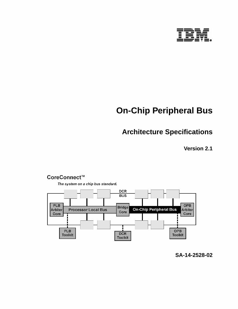
The on-chip peripheral bus (OPB) is designed for easy connection of on-chip peripheral devices. It provides a common design point for various on-chip peripherals. The OPB is a fully synchronous bus which functions independently at a separate level of bus hierarchy. It is not intended to connect directly to the processor core. The processor core can access the slave peripherals on this bus through the PLB to OPB bridge unit which is a separate core. See the PLB to OPB bridge core specification for more information. Peripherals which are OPB bus masters can access memory on the PLB through the OPB to PLB bridge unit which is a separate core. See the OPB to PLB bridge core specification for more information.
The on-chip peripheral bus has the following features:
• Up to a 64-bit address bus
• 32-bit or 64-bit data bus implementations
• Fully synchronous
• Provides support for 8-bit, 16-bit, 32-bit, and 64-bit slaves
• Provides support for 32-bit and 64-bit masters
• Dynamic bus sizing; byte, halfword, fullword, and doubleword transfers
• Optional Byte Enable support
• Uses a distributed multiplexer method of attachment instead of threestate drivers, to ease manufacturing test. Address and data buses may be implemented in distributed AND-OR gates or as a dotted bus
• Byte and halfword duplication for byte and halfword transfers
• Single cycle transfer of data between OPB bus master and OPB slaves
• Sequential address protocol support
• Devices on the OPB may be memory mapped, act as DMA peripherals, or support both transfer methods
• A 16-cycle fixed bus timeout provided by the OPB arbiter
• OPB slave is capable of disabling the fixed timeout counter to suspend bus timeout error
• Support for multiple OPB bus masters
• Bus parking for reduced latency
• OPB masters may lock the OPB bus arbitration
• OPB slaves capable of requesting retry to break possible arbitration deadlock
• Bus arbitration overlapped with last cycle of bus transfers
Version 2.1 OPB Overview 1

Figure 1 demonstrates how the on-chip peripheral bus is interconnected for the purpose of Core+ASIC development or system-on-a-chip design.
As shown in Figure 1, the on-chip bus structure provides a link between the processor core and other peripherals which consist of PLB and OPB master and slave devices.
The processor local bus (PLB) is the high performance bus used to access memory through the bus interface units. The two bus interface units shown above: external peripheral controller and memory controller are the PLB slaves. The processor core has two PLB master connections, one for instruction cache and one for data cache. Attached to the PLB is also the direct memory access (DMA) controller, which is a PLB master device used in data intensive applications to improve data transfer performance.
Lower performance peripherals (such as OPB master, slave, and other internal peripherals) are attached to the on-chip peripheral bus (OPB). A bridge is provided between the PLB and OPB to enable data transfer by PLB masters to and from OPB slaves. The PLB to OPB bridge is a slave on the PLB and a master on the OPB. A bridge is provided between the OPB and PLB to enable data transfer by OPB masters to and from PLB slaves. The OPB to PLB bridge is a slave on the OPB and a master on the PLB. DMA slave peripherals are also supported on the OPB.
The device control register (DCR) bus is used primarily for accessing status and control registers within the various PLB and OPB masters and slaves. It is meant to off-load the PLB from the lower performance status and control register read and write transfers. The DCR bus architecture allows data transfers to occur independent of PLB and OPB transfers.
On-
Chi
p P
erip
hera
l Bus
Processor Local Bus
OPB
PLB
OPB
Internal
OPBMaster
Slave
Peripheral
PLB to OPBBridge
Figure 1. On-chip Peripheral Bus Interconnection
DC
R B
usD
CR
Bus
Arbiter
Arb
iter
Processor Core
Data InstructionCache UnitCache Unit
OPB to PLBBridge
Memory Controller
SDRAMController
External Peripheral Controller
ExternalPeripheral
ExternalBus Master
DMAController DCR Bus
SRAMROM
DCR Bus
2 On-Chip Peripheral Bus Version 2.1

1.1 Physical Implementation
Figure 2 shows a physical implementation of the OPB. Since the OPB supports multiple master devices, the address bus and data bus are implemented as a distributed multiplexer. This design will enable future peripherals to be added to the chip without changing the I/O on either the OPB arbiter or the other existing peripherals. By specifying the bus qualifiers as I/O for each peripheral (select for the ABus, DBusEn for the DBus), the bus can be implemented in a variety of ways, that is, as a distributed ring mux (shown below), using centralized AND/OR’s or multiplexers, using transceiver modules and a dotted bus, etc. The optimal design for each implementation will vary, depending on the number of devices attached to the OPB and timing and routing constraints.
AN
D
OPB_DBus(32:63)
OPB_ABus
Sl0_DBus(0:31)
OPB BridgeMaster Device OPB Bridge
Slave Device
Figure 2. Physical Implementation of the OPB
Sl0_DBusEn
Sl0_DBus(32:63)
Sl0_DBusEn32_63AN
D
AN
D
M0_DBus(0:31)
M0_DBusEn
AN
D
M0_DBus(32:63)
M0_DBusEn32_63
AN
DM0_ABus
M0_Select
OPB_DBus(0:31)
AN
D
OPB_DBus(32:63)
OPB_ABus
Sl1_DBus(0:31)OPB
Master Device
OPB Slave Device
Sl1_DBusEn
Sl1_DBus(32:63)
Sl1_DBusEn32_63AN
D
AN
D
M1_DBus(0:31)
M1_DBusEn
AN
D
M1_DBus(32:63)
M1_DBusEn32_63
AN
D
M1_ABus
M1_Select
OPB_DBus(0:31)
OR
OPB
OR
OR
Arbiter
M0_request
OPB_M0Grant
M1_request
OPB_M1Grant
Version 2.1 OPB Overview 3

Control signals from OPB masters and slaves to and from the OPB arbiter and the peripherals will be similarly OR’ed together, and then sent to each device. Bus arbitration signals such as Mn_request and OPB_MnGrant are directly connected between the OPB arbiter and each OPB master device.
The following three tables show OPB output signal connection. These tables show the OPB bus logic used to combine signals from each master and slave device, to distribute to other master and slave devices.
Table 1 describes master output connection.
Table 1. Master Output Connection
Signal To Bus Logic Gated By (AND)
Mn_request Mn_request Direct Ungated
Mn_busLock OPB_busLock OR Ungated
Mn_select OPB_select OR Ungated
Mn_RNW OPB_RNW AND-OR Mn_select
Mn_BE OPB_BE AND-OR Mn_select
Mn_hwXfer OPB_hwXfer AND-OR Mn_select
Mn_fwXfer OPB_fwXfer AND-OR Mn_select
Mn_dwXfer OPB_dwXfer AND-OR Mn_select
Mn_seqAddr OPB_seqAddr AND-OR Mn_select
Mn_ABus OPB_ABus AND-OR Mn_select
Mn_UABus OPB_UABus AND-OR Mn_select
Mn_DBus(0:31) OPB_DBus(0:31) AND-OR Mn_DBusEn
Mn_DBusEn Qualifies DBus(0:31) Ungated
Mn_DBus(32:63) OPB_DBus(32:63) AND-OR Mn_DBusEn32_63
Mn_DBusEn32_63 Qualifies DBus(32:63) Ungated
Sln_dmaReq Sln_dmaReq Direct Ungated
4 On-Chip Peripheral Bus Version 2.1

Table 2 describes slave output connection.
Table 3 describes arbiter output connection.
Table 2. Slave Output Connection
Signal To Bus Logic Gated By (AND)
Sln_xferAck OPB_xferAck OR Ungated
Sln_hwAck OPB_hwAck4 OR Ungated
Sln_fwAck OPB_fwAck OR Ungated
Sln_dwAck OPB_dwAck OR Ungated
Sln_errAck OPB_errAck OR Ungated
Sln_retry OPB_retry OR Ungated
Sln_toutSup OPB_ToutSup OR Ungated
Sln_DBus(0:31) OPB_DBus(0:31) AND-OR Sln_DBusEn
Sln_DBusEn Qualifies DBus N/A Ungated
Sln_DBus(32:63) OPB_DBus(32:63) AND-OR Sln_DBusEn32_63
Sln_DBusEn32_63 Qualifies DBus(32:63) N/A Ungated
Sln_dmaReq Sln_dmaReq Direct Ungated
Table 3. Arbiter Output Connection
Signal To Bus Logic
OPB_MnGrant OPB_MnGrant Direct
OPB_timeout OPB_timeout Direct
Version 2.1 OPB Overview 5

Chapter 2. OPB Signals
OPB signals can be grouped under the following categories:
– Arbitration Signals
– Bus Signals
– Data Transfer Control Signals
– DMA Peripheral Support Signals (Optional)
2.1 Signal Naming Conventions
The implementation of the OPB consists of an OPB arbiter, and a combination of OPB master and slave devices, connected at the chip level by bus logic (AND and OR gates). Slaves which are connected to the OPB use the following naming convention:
• Signals which are outputs of the OPB bus logic and inputs to the master and slave devices are prefixed with OPB_. There is only one output of the bus logic for each one of these signals and it is received as an input by each relevant device attached on the OPB. For example, OPB_RNW is an output of the OPB bus logic and is an input to each slave attached to the OPB.
• Signals which are outputs of the OPB slaves and inputs to the OPB bus logic are prefixed with Sln_. Each slave has its own output which is an input to the OPB bus logic, where it is logically OR’ed together to form a single signal. The slaves must ensure that these signals are driven to a logic ‘0’ when they are not involved in a transfer on the OPB (with the exception of Sln_DBus, which need not be driven to a “0” when inactive, but which is qualified with Sln_DBusEn). For example, Sln_xferAck is an output of each slave attached to the OPB, there are multiple Sln_xferAck inputs to the OPB bus logic, and they are OR’ed together to form OPB_xferAck, which is output to all OPB masters.
Each master is attached directly to the OPB bus logic with its own address, read data, and write data buses and control signals, and these signals use the following naming convention:
• Signals which are driven by a master as an input to the OPB bus logic are pre-fixed with Mn_. For example, Mn_request signal when implemented would result in M0_request, M1_request, etc., up to the maximum number of masters supported (implementation dependent).
• Signals which are driven by the OPB arbiter to a specific master have a prefix OPB_Mn to indicate that this signal is from the OPB arbiter to a specific master (i.e. OPB_MnGrant). The OPB arbiter provides an output for this signal for each master attached to the bus. For example, the OPB_MnGrant signal, when implemented would result in OPB_M0Grant, OPB_M1Grant, etc., up to the maximum number of masters supported (implementation dependent).
• Signals which are driven by the OPB bus logic to all master and slave devices are prefixed with OPB_. There is only one output of the OPB bus logic for each one of these signals and it is received as an input by each relevant device attached on the OPB. For example, OPB_select is an output of the OPB bus logic and is an input to each slave device attached to the OPB.
Table 4 provides a summary of all OPB input/output signals in alphabetical order, the interfaces under which they are grouped, followed by a brief description and page reference for detailed functional
6 On-Chip Peripheral Bus Version 2.1

description. Note that some signals may not be required for a particular master, slave, or bus implementation. See “Optional Signal Enumeration” on page 18 for details.
Table 4. Summary of OPB Signals
Signal Name Interface I/O Description Page
DMA_SlnAck DMA O DMA slave acknowledge (OPTIONAL) 17
Mn_ABus Master O Master address bus 11
Mn_BE M/A O Master Byte Enables (OPTIONAL) 16
Mn_beXfer Master O Master byte enable transfer (OPTIONAL) 16
Mn_busLock M/A O Master bus arbitration lock (OPTIONAL) 9
Mn_DBus Master O Master data bus 13
Mn_DBusEn Master O Master data bus enable 13
Mn_DBusEn32_63 Master O Master data bus enable bits 32:63 (OPTIONAL) 14
Mn_dwXfer Master O Master doubleword transfer 13
Mn_fwXfer Master O Master fullword transfer 13
Mn_hwXfer Master O Master halfword transfer 13
Mn_request Master O Master bus request 8
Mn_RNW Master O Master read not write 12
Mn_select Master O Master select 12
Mn_seqAddr Master O Master sequential address 13
Mn_UABus Master O Master upper address bus (OPTIONAL) 11
OPB_ABus M/S I OPB address bus 11
OPB_BE Slave I OPB Byte Enables (OPTIONAL) 16
OPB_beXfer Slave I OPB byte enable transfer (OPTIONAL) 16
OPB_beAck Master I OPB byte enable acknowledge (OPTIONAL) 16
OPB_busLock Arbiter I OPB bus arbitration lock 9
OPB_DBus M/S I OPB data bus 13
OPB_errAck Master I OPB error acknowledge 15
OPB_dwAck Master I OPB doubleword acknowledge 14
OPB_dwXfer Slave I OPB doubleword transfer 13
OPB_fwAck Master I OPB fullword acknowledge 14
OPB_fwXfer Slave I OPB fullword transfer 13
OPB_hwAck Master I OPB halfword acknowledge 14
OPB_hwXfer Slave I OPB halfword transfer 13
OPB_MnGrant M/A I OPB master bus grant 9
OPB_pendReqn Master I OPB pending master request (OPTIONAL) 9
OPB_retry Master I OPB bus cycle retry 10
OPB_RNW Slave I OPB read not write 12
OPB_select S/A I OPB select 12
OPB_seqAddr Slave I OPB sequential address 13
Version 2.1 OPB Signals 7

2.2 Arbitration Signals
OPB bus arbitration among requesting master devices is performed by the OPB arbiter. Each master connects directly to the arbiter through Mn_request and OPB_MnGrant signals. The arbiter also receives OPB_busLock, OPB_select, and OPB_xferAck to monitor bus activity for arbitration. The OPB arbiter defines two valid types of arbitration cycles:
1. Idle
OPB_select and OPB_busLock are deasserted, indicating no data transfer in progress.
2. Overlapped Arbitration Cycle
OPB_XferAck is asserted, indicating the final cycle in a data transfer, and OPB_busLock is not asserted. Arbitration in this cycle allows another master to begin a transfer in the following cycle, avoiding the need for a “dead” cycle on the bus.
Grants are issued to masters (requesting or parked) only during valid arbitration cycles. Locking masters receive grants during valid arbitration cycles in response to requests, while the bus is locked.
2.2.1 Mn_request (Master Bus Request)
The Mn_request signal is asserted by an OPB master to request control of the bus, which is granted by the OPB arbiter via the OPB_MnGrant signal. For single transfers, Mn_request should normally be deasserted during the first or only cycle during which the bus is to be used by the device. If an OPB master requires continuous data transfer cycles, it can continue to assert Mn_request, and then deassert Mn_request during the first or only cycle of the last data transfer. Continuous assertion of
OPB_timeout M/A I OPB timeout error 10
OPB_toutSup Arbiter I OPB timeout suppress 15
OPB_xferAck M/A I OPB transfer acknowledge 14
OPB_UABus M/S I OPB upper address bus (OPTIONAL) 11
Sln_beAck Slave O Slave byte enable acknowledge (OPTIONAL) 16
Sln_DBus Slave O Slave data bus 11
Sln_DBusEn Slave O Slave data bus enable 13
Sln_DBusEn32_63 Slave O Slave data bus enable (OPTIONAL) 14
Sln_dmaReq DMA O Slave DMA request (OPTIONAL) 17
Sln_errAck Slave O Slave error acknowledge (OPTIONAL) 15
Sln_dwAck Slave O Slave doubleword acknowledge 14
Sln_fwAck Slave O Slave fullword acknowledge 14
Sln_hwAck Slave O Slave halfword acknowledge 14
Sln_retry Slave O Slave bus cycle retry (OPTIONAL) 10
Sln_toutSup Slave O Slave timeout suppress (OPTIONAL) 15
Sln_xferAck Slave O Slave transfer acknowledge 14
Table 4. Summary of OPB Signals (Continued)
Signal Name Interface I/O Description Page
8 On-Chip Peripheral Bus Version 2.1

Mn_request does not assure uninterrupted access to the OPB; the bus lock signal is provided to accomplish this.
2.2.2 OPB_pendReqn (OPB Pending Master Request)
The OPB_pendReqn signal indicates to a master that one, or more, of the other masters attached to the bus is requesting access to the bus to perform transfers. This signal is formed by ORing together all master requests on the bus except a masters own. This signal is used by masters performing long locked transfers in conjunction with the Master Latency counter to determine whether or not they must relinquish control of the bus. See “OPB Master Latency” on page 72 for details on its use. This logic can be implemented internal or external to the OPB arbiter.
2.2.3 OPB_busLock, Mn_busLock(OPB Bus Arbitration Lock)
OPB bus arbitration is “locked” whenever OPB_busLock is active. The OPB arbiter will arbitrate among requesting masters during valid arbitration cycles only when OPB_busLock is inactive. While locked, the OPB Arbiter will continue to grant the bus to the OPB master device asserting the Mn_busLock signal, without regard to the priority of the device or other devices with concurrent requests for the bus.
The Mn_busLock signal must be asserted by an OPB master in the clock following the sampling of the master’s asserted OPB_MnGrant signal. The Mn_busLock signal may be deasserted at any time. Typically it will be deasserted during the final data transfer cycle of a master’s sequence of transfers, to allow for overlapped bus arbitration.
The bus master which asserts Mn_busLock may proceed to the next data transfer cycle without bus arbitration. Lock has the effect of freezing the arbiter in its current state, i.e., granted to the locking master. Thus, Mn_request and OPB_MnGrant have no effect on bus arbitration while the bus is locked, although a master will typically continue to assert Mn_request, and OPB_MnGrant will continue to be asserted during valid arbitration cycles. The master could deassert Mn_select, ending the transfer in progress, but would still be “granted” the bus by the arbiter as long as Mn_busLock remains asserted. Desertion of Mn_busLock results in bus arbitration during the next valid bus arbitration cycle, which may be the same cycle in which Mn_busLock is deasserted. By deasserting Mn_busLock prior to the final data transfer cycle, the asserting master potentially allows another master to proceed with a separate data transfer cycle with no intervening “dead” cycle on the OPB. See “Bus Lock Signal Penalty Case” on page 45 for details.
DMA peripheral transfers perform data transfers across the OPB without the use of the Mn_select or Mn_Abus signals. In this case the DMA will request the bus and use the Mn_busLock signal to retain ownership until the setup, wait, and hold time of the peripheral transfer have been completed. The DMA should assert the DMA_SlnAck signal to the peripheral device as soon as possible
Masters should avoid locking the OPB prior to being ready to perform data transfers. Also masters should avoid inserting idle cycles between subsequent data transfer cycles. Masters which lock the OPB for large number of transfer, or long periods of time, must implement an OPB master latency timer.
2.2.4 OPB_MnGrant (OPB Master Bus Grant)
The OPB_MnGrant signal is asserted by the OPB Arbiter to grant control of the bus to a master device requesting it. The master may begin to drive signals on the OPB in the cycle following the
Version 2.1 OPB Signals 9
assertion of OPB_MnGrant. All OPB masters should examine their bus grant signals at the rise of the OPB Clock, and may not proceed to initiate a bus cycle unless it is asserted (or unless they have locked the bus). The OPB_MnGrant signal will only be asserted during a valid arbitration cycle, as defined above.
If a master has locked the bus via OPB_busLock, that master retains control of the OPB and no other master requests will be granted. The locking master’s grant signal will be asserted in response to its request during valid arbitration cycles, but the assertion of request and grant have no effect on bus arbitration for the duration of the bus lock condition.
The OPB supports bus parking. If no requests are pending during a valid OPB arbitration cycle, the OPB Arbiter may “park” on one master, asserting that master’s grant signal. This allows the parked master to proceed with a data transfer cycle without incurring the delay of performing an arbitration cycle, if no other master is requesting. A parked master may proceed to initiate a bus transfer cycle by asserting Mn_select, if its grant signal was asserted in the previous cycle, without the delay of asserting request and awaiting a valid grant.
The enabling of the bus parking feature, and determination of which master the OPB Arbiter will park on, are implementation dependent.
2.2.5 OPB_timeout (OPB Timeout Error)
The OPB_timeout signal is an output of the OPB Arbiter. OPB_timeout is an input to all master devices on the OPB, and is used to indicate that a timeout error has occurred. This signal will be asserted in the 16th cycle following the assertion of OPB_select if there is no response from a slave (OPB_xferAck or OPB_retry), and if ToutSup is not asserted by an addressed slave device to suppress the timeout. Upon assertion of OPB_timeout, the master device which initiated the transfer cycle must terminate the transfer by deasserting Mn_select signal in the cycle following the assertion of OPB_timeout. If OPB_busLock is not asserted, the OPB Arbiter will perform a bus arbitration in the cycle in which OPB_select is deasserted. If OPB_busLock is asserted, the requesting master retains control of the OPB, but must still deassert Mn_select following the assertion of OPB_timeout for at least one cycle.
If OPB_xferAck or OPB_retry are asserted in the 16th cycle following select, coincident to the assertion of OPB_timeout, the master device should ignore OPB_timeout, and respond to the slave’s OPB_xferAck or OPB_retry signal.
2.2.6 OPB_retry, Sln_retry(OPB Bus Cycle Retry)
The Bus Cycle Retry signal is asserted by an OPB slave to indicate that it is unable to perform the requested transfer at this time. The primary use of this signal is to permit resolution of a deadlock condition which may occur as a result of system implementations that include buses which operate independently.
An OPB slave will assert the Sln_retry signal instead of the Sln_xferAck signal when a situation requiring it is detected. It must remain asserted until the slave becomes deselected as a result of the OPB_select signal being deasserted. Sln_retry will cause the requesting master to terminate the transfer by deasserting Mn_select, and if asserted Mn_request and Mn_busLock, in the cycle following the detection of the OPB_retry signal. The master’s Mn_select, Mn_request, and Mn_busLock must remain deasserted for one cycle, during which the OPB Arbiter will re-arbitrate the bus.
10 On-Chip Peripheral Bus Version 2.1

A slave asserting Sln_retry must not assert Sln_xferAck.
Sln_retry must be asserted within 16 cycles of OPB_select to avoid a timeout, unless Sln_ToutSup is asserted. If OPB_retry and OPB_timeout are received simultaneously by a master device (i.e., Sln_retry was asserted in the 16th cycle following OPB_select), the master should ignore OPB_timeout and act on OPB_retry as appropriate
2.3 Bus Signals
2.3.1 OPB_ABus(0:31), Mn_ABus(0:31) (OPB Address Bus)
The OPB_ABus is used by bus masters to select a unique OPB slave attached to the OPB. The 32 lines of the address bus form a binary number which represents an address. This address will specify a one to one mapping of device functions, peripheral registers, or storage functions contained within devices which are attached to the bus.
The most significant bit of the address bus will be carried by bit 0 and the least significant bit of the address will be carried by bit 31. The most significant byte of a halfword or fullword will be the byte which corresponds to the smallest binary address.
The Mn_ABus signals from each OPB Master are AND’ed with that master’s Mn_select, and the resulting buses from all OPB masters are then OR’ed together to form OPB_ABus. Thus, a master device may continue to drive data onto Mn_ABus when its select is not asserted.
See “Physical Implementation” on page 3 for details on address and data bus connections.
2.3.2 OPB_UABus(0:31), Mn_UABus(0:31) (OPB Upper Address Bus)
The OPB_UABus is used to form the most significant portion of a 64-bit address. The 32 lines of the upper address bus concatenated with 32 lines from the OPB_ABus form a 64-bit binary number which represents an address. For example if OPB_ABus(0:31) = 32’h89ABCDEF and OPB_UABus(0:31) = 32’h01234567 the 64-bit address generated is 64’h0123456789ABCDEF.
The Mn_UABus signals from each OPB Master are AND’ed with that master’s Mn_select, and the resulting buses from all OPB masters are then OR’ed together to form OPB_UABus. Thus, a master device may continue to drive data onto Mn_UABus when its select is not asserted.
Note: All 64-bit address bits do not need to be implemented. Partial upper address implementations are possible. For example a 36-bit OPB implementation would only require the implementation of OPB_UABus(28:31) and Mn_UABus(28:31).
2.3.3 OPB_DBus, Mn_DBus, Sln_DBus (OPB Data Bus)
The OPB_DBus is used to transfer data between OPB masters and slaves. 32-bit and 64-bit data bus implementations are possible. The 32-bit data bus consists of signals (0:31). Bit 0 is the most significant bit, and bit 31 is the least significant bit. The 64-bit data bus consists of signals (0:63). Bit 0 is the most significant bit, and bit 63 is the least significant bit. When subdivided into bytes, Bits 0-7 represent the most significant byte on the data bus.
The Mn_DBus(0:31) and Sln_DBus(0:31) signals from each OPB device are AND’ed with that device’s Mn_DBusEn or Sln_DBusEn, respectively, and the resulting buses from all OPB devices are then OR’ed together to form OPB_DBus(0:31). The Mn_DBus(32:63) and Sln_DBus(32:63) signals
Version 2.1 OPB Signals 11
from each OPB device are AND’ed with that device’s Mn_DBusEn32_63 or Sln_DBusEn32_63, respectively, and the resulting buses from all OPB devices are then OR’ed together to form OPB_DBus(32:63). See “Physical Implementation” on page 3 for details on address and data bus connections.
2.4 Data Transfer Control Signals
2.4.1 OPB_select, Mn_select (OPB Select)
The Mn_select is driven by an OPB master in the cycle following the assertion of that master’s OPB_MnGrant signal to assume control of the bus and to indicate that a valid data transfer cycle is in progress. The Mn_select signal qualifies all master control signals and is the enable for Mn_ABus(0:31), Mn_UABus(0:31), Mn_BE, Mn_RNW, Mn_hwXfer, Mn_fwXfer, Mn_dwXfer, Mn_beXfer, and Mn_seqAddr. Mn_select will continue to be driven until the master receives OPB_xferAck, OPB_retry, or OPB_timeout.
A master who has assumed control of the bus may terminate, or abort, the transfer cycle at any time by deasserting Mn_select. All slaves are required to terminate the transfer in progress and reset their state machines if the select signal is deactivated. If the master deasserts Mn_select and Mn_busLock is not asserted the master must also relinquish the bus. If the master deasserts Mn_select and Mn_busLock is asserted the master retains ownership of the bus. If the select is deactivated in the cycle in which the slave would have activated the Sln_xferAck or Sln_retry signal, then the slave must deactivate the Sln_xferAck or Sln_retry signal in this cycle.
2.4.2 OPB_RNW, Mn_RNW (OPB Read Not Write)
The OPB_RNW signal indicates the direction of data transfer. The signal must be valid any time that Select is active. If the signal is high the request is for the OPB slave to supply data to be read into the master. If the signal is low the request is for the OPB slave to accept write data from the master. For a write operation the first data to be transferred must be placed on Mn_DBus when Mn_select is asserted.
12 On-Chip Peripheral Bus Version 2.1

2.4.3 Mn_hwXfer,OPB_hwXfer, Mn_fwXfer, OPB_fwXfer, Mn_dwXfer,OPB_dwXfer (OPB Transfer Size)
The Transfer Size signals are asserted by the bus master to indicate the size of the requested transfer. They are used in conjuction with the OPB_hwAck, OPB_fwAck, and OPB_dwAck signals from the slave to implement Dynamic Bus Sizing on the OPB. Note that since smaller width slaves do not have the larger width transfer size inputs masters are responsible for asserting all possible smaller width slave transfer sizes with each request. All other combinations of these signals are reserved. Masters only need to implement transfer size signals up to the maximum request size they will make. For example a 32-bit Master can’t make a doubleword transfer request. Therefore in this case the master does not implement the Mn_dwXfer signal.
2.4.4 OPB_seqAddr, Mn_seqAddr (OPB Sequential Address)
To reduce access latency for sequential addresses, the OPB_seqAddr signal is provided. The Mn_seqAddr signal is asserted by the bus master to indicate that the transfer being performed will be followed with a transfer to the next sequential address in the same direction, read or write. The slave which receives the OPB_seqAddr signal may assume that there will be no intervening bus operations to addresses other than the next sequential address and that the next transfer will be in the same direction.
This signal is always used in conjuction with the bus arbitration lock in order to guarantee that there are no intervening bus operations that might occur to non-sequential addresses.
This signal is a transfer qualifier. It must be asserted at the beginning of a transfer, with OPB_select, OPB_ABus, OPB_UABus, OPB_hwXfer, OPB_fwXfer, OPB_dwXfer, OPB_BE, OPB_beXfer, and OPB_RNW. It may be deasserted in any subsequent clock cycle. Slaves which sample this signal asserted when asserting xferAck assume the next transfer will be to the next sequential address in the same direction, read or write.
This signal should be negated by the master in the clock cycle following the second to last xferAck along with busLock to allow pipelined arbitration to occur.
The Mn_seqAddr signal may be negated simultaneously with the negation of Mn_select in any cycle. The slave is required to terminate the transfer in progress. In general this should be avoided as it creates an arbitration penalty cycle if the busLock signal is also negated.
This signal can help the bus slave to avoid address decode cycle, to improve data transfer performance. If OPB slave device ignores this signal, the data transfer proceeds normally.
2.4.5 Mn_DBusEn, Sln_DBusEn (Master Data Bus Enable)
Mn_DBusEn and Sln_DBusEn signals are used to enable a master or slave device’s data onto the OPB data bus(0:31) during write and read transfers, respectively. The Mn_DBus(0:31) and
Table 5. OPB_hwXfer, OPB_fwXfer, OPB_dwXfer Encoding
Transfer Size OPB_hwXfer OPB_fwXfer OPB_dwXfer
Byte 0 0 0
Halfword 1 0 0
Fullword 1 1 0
Doubleword 1 1 1
Version 2.1 OPB Signals 13
Sln_DBus(0:31) bus are AND’ed with these signals prior to being OR’ed together with other devices’ data buses to form OPB_DBus(0:31). Master and slave devices may thus continuously drive their data output buses, and only drive the enable signals during valid transfer cycles. It is suggested however that master and slave devices drive 0 on unused data bus byte lanes. This conserves power by preventing switching of these OPB_DBus byte lanes when the data bus is enabled. See “Physical Implementation” on page 3 for details on address and data bus connections.
2.4.6 Mn_DBusEn32_63, Sln_DBusEn32_63 (Master Data Bus Enable)
Mn_DBusEn32_63 and Sln_DBusEn32_63 signals are used to enable a 64-bit master or 64-bit slave device’s data onto the OPB data bus(32:63) during write and read transfers, respectively. The Mn_DBus(32:63) and Sln_DBus(32:63) bus are AND’ed with these signals prior to being OR’ed together with other devices’ data buses to form OPB_DBus(32:63). Master and slave devices may thus continuously drive their data output buses, and only drive the enable signals during valid transfer cycles. It is suggested however that master and slave devices drive 0 on unused data bus byte lanes. This conserves power by preventing switching of these OPB_DBus byte lanes when the data bus is enabled. If a 64-bit master or slave is not transferring data on Mn_DBus(32:63) or Sln_DBus(32:63) respectively the Mn_DBusEn32_63 or Sln_DBusEn32_63 signals should not be asserted in order to conserve power consumption. See “Physical Implementation” on page 3 for details on address and data bus connections.
2.4.7 OPB_xferAck, Sln_xferAck (OPB Transfer Acknowledge)
The Transfer Acknowledge signal is asserted by the addressed slave to indicate the completion of a data transfer between the OPB master and the OPB slave. It is asserted for one and only one cycle per data transfer. In the case of write operations, this means that the slave has accepted the data which presently appears on the data bus, or will do so at the end of this cycle. In the case of read operations, this means that the slave has placed the data to be transferred to the OPB master on the data bus or will drive the data on the data bus prior to the end of this cycle. Transfer Acknowledge qualifies the device width control signals Sln_hwAck and Sln_fwAck, and the Error Acknowledge signal Sln_errAck. Sln_xferAck must be asserted within 16 cycles of OPB_select to prevent a timeout (unless Sln_ToutSup is asserted).
Sln_xferAck must not be asserted if Sln_retry is asserted.
If Sln_xferAck is asserted in the same cycle in which OPB_timeout is asserted, the requesting master should ignore the OPB_timeout signal and complete the data transfer.
2.4.8 OPB_hwAck, Sln_hwAck, OPB_fwAck, Sln_fwAck,OPB_dwAck, Sln_dwAck (OPB Transfer Size Acknowledge)
The Transfer Size Acknowledge signals are asserted by a bus slave to indicate its device width (i.e., which bits of the data bus it is utilizing). All byte devices are attached to DBus[0:7]; halfword devices are attached to DBus[0:15], fullword devices are attached to DBus[0:31], and doubleword devices are attach DBus[0:63]. These signals are used in conjuction with the OPB_hwXfer, OPB_fwXfer, and OPB_dwXfer signals from the master to implement Dynamic Bus Sizing on the OPB.
Sln_hwAck, Sln_fwAck, and Sln_dwAck may be asserted immediately upon a slave device’s decode of its address during a transfer cycle (OPB_select asserted). They must be valid when Sln_xferAck is asserted. Note that in the case of a doubleword slave it must assert both the Sln_dwAck and the Sln_fwAck signals. This is because 32-bit masters do not sample the OPB_dwAck signal and
14 On-Chip Peripheral Bus Version 2.1

therefore assume in this case the slave is 32-bits wide. All other combinations of these signals are reserved. Table 6 shows the encoding for the Transfer Size Acknowledge signals. Slaves only need to implement transfer acknowledge signals up to the maximum size transfer they will make. For example a 32-bit Slave can’t fulfil a doubleword transfer request. Therefore in this case the slave does not implement the Sln_dwAck signal.
2.4.9 OPB_errAck, Sln_errAck (OPB Error Acknowledge)
The Error Acknowledge signal is asserted by a bus slave to indicate that the slave encountered an error in performing the requested transfer. Sln_errAck may be asserted immediately upon a slave device’s decode of its address during a transfer cycle (OPB_select asserted) or any time thereafter. It must be valid when Sln_xferAck is asserted. The OPB_errAck signal is formed by ORing together all Sln_errAck signals from the slaves attached to the bus. Slaves must drive their Sln_errAck signal only when selected, otherwise the slave must keep its Sln_errAck signal deasserted.
2.4.10 OPB_toutSup, Sln_toutSup (Slave Time-out Suppress)
The Time-out Suppress signal is asserted by an OPB slave to indicate to the OPB Arbiter that the bus operation will be delayed for an extended period of time. This signal must be asserted within 16 clock cycles from the assertion of OPB_select to prevent a bus timeout. Sln_ToutSup will be used by the OPB Arbiter to disable the timeout counter and suppress the assertion of OPB_timeout. Sln_ToutSup must remain asserted until the slave can complete the requested operation.
Note: If the master deasserts OPB_select prior to the slave asserting Sln_xferAck or Sln_retry, thereby aborting the transfer request, the Sln_toutSup signal may remain asserted for one additional clock cycle. See “OPB Master Abort” on page 49.
Table 6. OPB_hwAck, OPB_fwAck, OPB_dwAck Encoding
Slave Device Width OPB_hwAck OPB_fwAck OPB_dwAck
Byte 0 0 0
Halfword 1 0 0
Fullword 0 1 0
Doubleword 0 1 1
Version 2.1 OPB Signals 15

2.5 Byte Enable Support Signals (Optional)
2.5.1 Mn_BE(0:7), OPB_BE(0:7) (Master Byte Enables)
Byte enables allow masters to perform unaligned multibyte operations in a single OPB transfer. During a transfer the assertion of a particular OPB_BE signal corresponds to a transfer request for the associated byte lane. Masters must assert the byte enable corresponding to the current transfer address at a minimum. Masters are required to assert the Mn_BE(0:7) signals with the assertion of Mn_select and the Mn_beXfer signals. The master must keep Mn_BE(0:7) asserted until sampling OPB_XferAck asserted or the deassertion of Mn_select. 32-bit Masters only drive Mn_BE(0:3) and 32-bit slaves only sample OPB_BE(0:3). Non-contiguous byte enables are not allowed. See “OPB Master Latency” on page 72. for a description of allowable byte enables.
2.5.2 Mn_beXfer, OPB_beXfer (Master Byte Enable Transfer Request)
The assertion Mn_beXfer is a request by the master to perform a byte enable transfer. The assertion of the OPB_beXfer is a request for the slave to transfer the byte lanes indicated via the asserted OPB_BE(0:7) signals. Masters which perform a byte enable transfer must assert Mn_beXfer with the assertion of Mn_select along with valid byte enables, Mn_BE(0:7). The Mn_beXfer signal must remain asserted until sampling OPB_XferAck asserted or the deassertion of the Mn_select signal. Masters are still responsible for correctly asserting the transfer size signals for the minimum aligned transfer in order to support slaves which do not support byte enables.
2.5.3 Sln_beAck, OPB_beAck (Slave Byte Enable Acknowledge)
The assertion of Sln_beAck incident with the Sln_XferAck signal indicates that the addressed slave has sampled the asserted OPB_beXfer signal and used the byte enables to transfer all contiguous bytes up to the size of the slave. Masters must sample the OPB_hwAck, OPB_fwAck, and OPB_dwAck signals to determine if their full request was accepted. Sln_beAck may be asserted immediately upon a slave’s decode of its address during a transfer cycle (OPB_select asserted). It must be valid when Sln_xferAck is asserted to signal a byte enable handshake acknowledge. If the master samples OPB_beAck deasserted incident with the assertion of OPB_XferAck it is assumed that the slave does not adhere to the byte enable architecture and the master must use the standard dynamic bus sizing operation of the OPB.
16 On-Chip Peripheral Bus Version 2.1

2.6 DMA Peripheral Support Signals (Optional)
The OPB supports optional DMA peripheral transfers. These transfer may be to a DMA peripheral attaches directly to the OPB bus or to a bus controller which has a DMA peripheral attached to it.
2.6.1 Sln_dmaReq (Slave DMA Request)
The Sln_dmaReq signal is asserted by a DMA peripheral to the DMA controller to request a data transfer. Before making the request, the DMA channel should have been programmed to indicate the device’s width, the device location, the transfer direction, the target address, and the timing parameters associated with the DMA peripheral.
2.6.2 DMA_SlnAck (DMA Slave Acknowledge)
The DMA Slave Acknowledge signal is asserted by the DMA controller to indicate to the DMA peripheral, or bus controller on behalf of the DMA peripheral, that it should drive or latch the OPB data bus. If the DMA transfer has been programmed to be a Read-From-Requesting device, the DMA peripheral, or bus controller on behalf of the DMA peripheral, should drive the OPB_Dbus with the data. If the DMA transfer has been programmed to be a Write-To-Requesting device the data on the OPB_Dbus is latched into the DMA peripheral, or bus controller on behalf of the DMA peripheral. In both cases, the data should be valid on the last cycle of DMA_SlnAck. This can be controlled by the Peripheral Wait Time parameter in the DMA channel control register. The Wait Time indicates the number of cycles that DMA_SlnAck should be asserted.
Version 2.1 OPB Signals 17

2.7 Optional Signal Enumeration
Note that signals labeled as (OPTIONAL) may not be required for a particular master, slave, or bus implementation. It is up to the master designer, slave designer, or system integrator to determine which signals to implement.
Table 7. Summary of OPB Signals
Signal Name Interface I/O Description Page
DMA_SlnAck DMA O DMA slave acknowledge is OPTIONAL. No DMA slaves may be attached to the OPB
17
Mn_BE M/A O Master Byte Enables is OPTIONAL. The master may not implement the Byte Enable protocol.
16
Mn_beXfer Master O Master byte enable transfer is OPTIONAL. The master may not implement the Byte Enable protocol.
16
Mn_busLock M/A O Master bus arbitration lock is OPTIONAL. The master may not need to lock the OPB.
9
Mn_DBusEn32_63 Master O Master data bus enable bits 32:63 is OPTIONAL. The master may only have a 32-bit data bus.
14
Mn_seqAddr Master O Master sequential address is OPTIONAL. The master may not perform sequential transfers.
13
Mn_UABus Master O Master upper address bus is OPTIONAL. The master may only have a 32-bit address bus.
11
OPB_BE Slave I OPB Byte Enables (OPTIONAL) No masters may implement the Byte Enable protocol.
16
OPB_beXfer Slave I OPB byte enable transfer (OPTIONAL) No masters may implement the Byte Enable protocol
16
OPB_beAck Master I OPB byte enable acknowledge (OPTIONAL) No masters may implement the Byte Enable protocol
16
OPB_pendReqn Master I OPB pending master request (OPTIONAL) No masters may implement a latency counter.
9
OPB_retry Master I OPB bus cycle retry. No slaves may implement the Sl_retry signal.
10
OPB_seqAddr Slave I OPB sequential address. No masters may implement this signal.
13
OPB_UABus M/S I OPB upper address bus (OPTIONAL). No master may implement any bits of the upper address bus.
11
Sln_beAck Slave O Slave byte enable acknowledge (OPTIONAL). The slave may not support the Byte Enable Protocol.
16
Sln_DBusEn32_63 Slave O Slave data bus enable (OPTIONAL). The slave may only have a 32-bit data bus.
14
Sln_dmaReq DMA O Slave DMA request (OPTIONAL). The slave may not be a DMA peripheral.
17
Sln_errAck Slave O Slave error acknowledge (OPTIONAL). The slave may not report any errors.
15
18 On-Chip Peripheral Bus Version 2.1

Sln_retry Slave O Slave bus cycle retry (OPTIONAL) 10
Sln_toutSup Slave O Slave timeout suppress (OPTIONAL) 15
Table 7. Summary of OPB Signals (Continued)
Signal Name Interface I/O Description Page
Version 2.1 OPB Signals 19

Chapter 3. OPB Interfaces
The OPB I/O signals are grouped under the following interface categories depending on their function. See “OPB Signals” on page 6 for detailed functional description.
– OPB Master Interface
– OPB Slave Interface
– OPB Arbiter Interface
– Optional DMA Interface
20 On-Chip Peripheral Bus Version 2.1
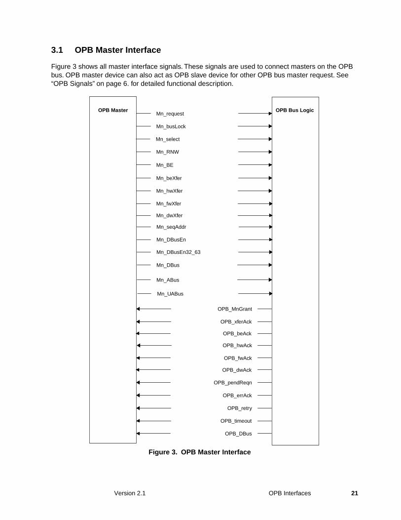
3.1 OPB Master Interface
Figure 3 shows all master interface signals. These signals are used to connect masters on the OPB bus. OPB master device can also act as OPB slave device for other OPB bus master request. See “OPB Signals” on page 6. for detailed functional description.
Mn_RNW
Mn_hwXfer
Mn_fwXfer
OPB_MnGrant
OPB_hwAck
OPB_xferAck
OPB_fwAck
Figure 3. OPB Master Interface
OPB_errAck
Mn_seqAddr
Mn_DBusEn
Mn_ABus
OPB Bus LogicOPB Master
OPB_retry
OPB_timeout
OPB_DBus
Mn_request
Mn_busLock
Mn_select
Mn_DBus
Mn_dwXfer
Mn_BE
Mn_DBusEn32_63
Mn_UABus
Mn_beXfer
OPB_dwAck
OPB_beAck
OPB_pendReqn
Version 2.1 OPB Interfaces 21

3.2 OPB Slave Interface
Figure 4 shows all OPB slave interface signals. These signals are used to connect slave devices on the OPB bus. This diagram also describes a fullword device with all 32 bits of OPB_DBus and Sln_DBus connected. Slave devices may also be of byte (8bit) or halfword (16 bit) widths. See “OPB Signals” on page 6. for detailed functional description
Sln_errAck
Sln_toutSup
Sln_retry
OPB_select
OPB_fwXfer
OPB_RNW
OPB_dwXfer
Figure 4. OPB Slave Interface
OPB_seqAddr
Sln_DBusEn
Sln_DBus
OPB Bus LogicOPB Slave
OPB_ABus
OPB_UABus
Sln_xferAck
Sln_hwAck
Sln_fwAck
Sln_dwAck
Sln_beAck
Sln_DBusEn32_63
OPB_BE
OPB_hwXfer
OPB_DBus
OPB_beXfer
22 On-Chip Peripheral Bus Version 2.1

3.3 OPB Arbiter Interface
Figure 5 shows all OPB arbiter interface input/output signals. These signals are used to connect OPB arbiter to the OPB bus. These signals are used to implement the OPB arbiter function. See “OPB Signals” on page 6. for detailed functional description
OPB_timeout
Mn_request
OPB_busLock
Figure 5. OPB Arbiter Interface
OPB_select
OPB Bus LogicOPB Arbiter
OPB_xferAck
OPB_toutSup
OPB_MnGrant
Version 2.1 OPB Interfaces 23

3.4 Optional DMA Interface
The optional DMA support consists of pairs of request and acknowledge signals as described below. In operation, a device will be connected to a particular DMA channel on the DMA controller by direct connection to the channels request and acknowledge signals.
Figure 6 shows all DMA input output signals. See “OPB Signals” on page 6 for detailed functional description
3.5 Connection of 32-bit and 64-bit devices
Interconnecting 64-bit masters and slaves to a 32-bit bus and 32-bit masters to a 64-bit bus requires some unique wiring. The attachment of fullword, halfword, and byte slaves is the same whether attached to a 32 or 64-bit OPB. The following diagrams illustrate the connection of 64-bit OPB devices and implementations.
DMA_SlnAck
Figure 6. Optional DMA Interface
DMA CoreOPB DMA
Sln_dmaReq
Peripheral Device
24 On-Chip Peripheral Bus Version 2.1

3.5.1 64-bit Master Attached To a 32-bit OPB bus
Figure 7 shows the 64-bit master interface signals to a 32-bit OPB implementation. Note the master OPB_dwAck input must be grounded. See “OPB Signals” on page 6. for detailed functional signal descriptions.
Mn_RNW
Mn_hwXfer
Mn_fwXfer
OPB_MnGrant
OPB_hwAck
OPB_xferAck
OPB_fwAck
Figure 7. 64-bit Master with 32-bit OPB
OPB_errAck
Mn_seqAddr
Mn_DBusEn
Mn_ABus(0:31)
32-bit OPB 64-bit OPB
OPB_retry
OPB_timeout
OPB_DBus(0:31)
Mn_request
Mn_busLock
Mn_select
Mn_DBus(0:31)
Bus LogicMaster
Mn_DBus(32:63) (NO CONNECT)
OPB_dwAck (GND)
Mn_DBusEn32_63 (NO CONNECT)
Mn_dwXfer (NO CONNECT)
OPB_pendReqn
Version 2.1 OPB Interfaces 25

3.5.2 64-bit Slave attached to a 32-bit OPB
Figure 8 shows a 64-bit slave interface to a 32-bit OPB implementation. Note that the slave OPB_dwXfer input signal must be grounded and the OPB_DBus(32:63) inputs must be connected to the data bus, OPB_DBus(0:31). See “OPB Signals” on page 6. for detailed functional signal descriptions
Sln_errAck
Sln_toutSup
Sln_retry
OPB_select
OPB_hwXfer
OPB_RNW
OPB_fwXfer
Figure 8. 64-bit Slave with 32-bit OPB
OPB_seqAddr
Sln_DBusEn
32-bit OPB64-bit OPB
OPB_ABus(0:31)
OPB_DBus(0:31)
Sln_xferAck
Sln_hwAck
Sln_fwAck
Bus Logic Slave
Sln_dwAck (NO CONNECT)
Sln_DBus(0:31)
Sln_DBusEn32_63 (NO CONNECT)
OPB_DBus(32:63)
OPB_dwXfer (GND)
Sln_DBus(32:63) (NO CONNECT)
26 On-Chip Peripheral Bus Version 2.1

3.5.3 32-bit Master Attached To a 64-bit OPB bus
Figure 9 shows the 32-bit master interface signals to a 64-bit OPB implementation. Note the master Mn_DBus(0:31) is also connected the Mn_DBus(32:63) bus input. The Mn_DBusEn32_63 bus input may be driven directly with Mn_DBusEn or optionally AND’ed with Mn_ABus(29) to conserve power as shown. See “OPB Signals” on page 6. for detailed functional signal descriptions.
Mn_RNW
Mn_hwXfer
Mn_fwXfer
OPB_MnGrant
OPB_hwAck
OPB_xferAck
OPB_fwAck
Figure 9. 32-bit Master with 64-bit OPB
OPB_errAck
Mn_seqAddr
Mn_DBusEn
Mn_ABus(0:31)
64-bit OPB 32-bit OPB
OPB_retry
OPB_timeout
OPB_DBus(0:31)
Mn_request
Mn_busLock
Mn_select
Mn_DBus(0:31)
Bus LogicMaster
Mn_DBus(32:63)
Mn_DBusEn32_63ANDMn_ABus(29)
OPB_pendReqn
Version 2.1 OPB Interfaces 27

3.5.4 32-bit Slave attached to a 64-bit OPB
Figure 10 shows a 32-bit slave interface to a 64-bit OPB implementation. Note that the Sln_DBus(0:31) signal is also connected the Sln_DBus(32:63) bus logic input. The Sln_DBusEn32_63 bus input may be driven directly with Sln_DBusEn or optionally AND’ed with OPB_ABus(29) to conserve power as shown. Also See “OPB Signals” on page 6. for detailed signal functional descriptions
Sln_errAck
Sln_toutSup
Sln_retry
OPB_select
OPB_hwXfer
OPB_RNW
OPB_fwXfer
Figure 10. 32-bit Slave with 64-bit OPB
OPB_seqAddr
Sln_DBusEn
64-bit OPB32-bit OPB
OPB_ABus(0:31)
OPB_DBus(0:31)
Sln_xferAck
Sln_hwAck
Sln_fwAck
Bus Logic Slave
Sln_DBus(0:31)
Sln_DBusEn32_63
Sln_DBus(32:63)
ANDOPB_ABus(29)
28 On-Chip Peripheral Bus Version 2.1

Chapter 4. OPB Timing Guidelines
The timing diagrams included in this specification are examples of operations on the OPB. All signals on the OPB are positive active and are either direct outputs of edge triggered latches which are clocked by the OPB clock, or are derived from the output of a register using several levels of combinatorial logic. All input signals should be captured in the OPB masters or OPB slaves on the rising edge of the OPB clock.
4.1 Timing Definitions
Begin Signal is valid within 8% of the clock cycle from the rise of the OPB clock signal.
Early Signal is valid within 18% of the clock cycle from the rise of the OPB clock signal.
Early + Signal is valid within 28% of the clock cycle from the rise of the OPB clock signal.
Middle - Signal is valid within 33% of the clock cycle from the rise of the OPB clock signal.
Middle Signal is valid within 43% of the clock cycle from the rise of the OPB clock signal.
Middle + Signal is valid within 53% of the clock cycle from the rise of the OPB clock signal.
Late - Signal is valid within 58% of the clock cycle from the rise of the OPB clock signal.
Late Signal is valid within 68% of the clock cycle from the rise of the OPB clock signal.
End Signal is valid within 78% of the clock cycle from the rise of the OPB clock signal.
Note: These definitions assume that there is 0ns of clock delay. For outputs, these delays represent the total logic delay from the C2 clock at the input to a register to the output of the core. For inputs, these delays represent the arrival time of the input relative to a 0ns delayed clock.
Set-up and Hold times for the OPB inputs and output delays for the OPB outputs are dependent on the technology and the physical implementation of the bus. These parameters are specified as a percentage of the bus clock cycle relative to the rise of the OPB clock.
Table 8 describes the OPB timing guidelines
Table 8. OPB Timing Guidelines
Signal Name Driven By Output Valid Received By
Mn_ABus Master n Begin OPB bus
Mn_busLock Master n Begin OPB bus
Mn_DBus Master n Early OPB bus
Mn_DBusEn Master n Early Bus gating logic
Mn_DBusEn32_63 Master n Early Bus gating logic
Mn_hwXfer Master n Begin OPB bus
Mn_fwXfer Master n Begin OPB bus
Mn_dwXfer Master n Begin OPB bus
Mn_beXfer Master n Begin OPB bus
Mn_BE Master n Begin OPB bus
Version 2.1 OPB Timing Guidelines 29

Mn_request Master n Begin OPB arbiter
Mn_RNW Master n Begin OPB bus
Mn_select Master n Begin OPB bus
Mn_seqAddr Master n Begin OPB bus
OPB_ABus OPB bus Early All slaves
OPB_busLock OPB bus Early All slaves
OPB_DBus OPB bus Late All masters and slaves
OPB_errAck OPB bus Middle + All masters
OPB_hwXfer OPB bus Early All slaves
OPB_hwAck OPB bus Middle + All masters
OPB_fwXfer OPB bus Early All slaves
OPB_fwAck OPB bus Middle + All masters
OPB_dwXfer OPB bus Early All slaves
OPB_dwAck OPB bus Middle + All masters
OPB_BE OPB bus Early All slaves
OPB_beXfer OPB bus Early All slaves
OPB_beAck OPB bus Middle + All masters
OPB_MnGrant OPB arbiter Late Master n
OPB_pendReqn OPB bus or arbiter Early All Masters
OPB_retry OPB bus Middle + All masters and OPB arbiter
OPB_RNW OPB bus Early All slaves
OPB_select OPB bus Early All slaves and OPB arbiter
OPB_seqAddr OPB bus Early All slaves
OPB_timeout OPB arbiter Middle All Masters
OPB_toutSup OPB bus Early + OPB arbiter
OPB_xferAck OPB bus Middle + All masters and OPB arbiter
Sln_DBus Slave Middle OPB bus
Sln_DBusEn Slave Middle Bus gating logic
Sln_DBusEn32_63 Slave Middle Bus gating logic
Sln_errAck Slave Middle OPB bus
Sln_hwAck Slave Middle OPB bus
Sln_fwAck Slave Middle OPB bus
Sln_dwAck Slave Middle OPB bus
Sln_retry Slave Middle OPB bus
Sln_toutSup Slave Early OPB bus
Sln_xferAck Slave Middle OPB bus
Sln_beAck Slave Middle OPB bus
Table 8. OPB Timing Guidelines (Continued)
Signal Name Driven By Output Valid Received By
30 On-Chip Peripheral Bus Version 2.1
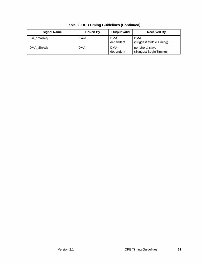
Sln_dmaReq Slave DMAdependent
DMA(Suggest Middle Timing)
DMA_SlnAck DMA DMAdependent
peripheral slave (Suggest Begin Timing)
Table 8. OPB Timing Guidelines (Continued)
Signal Name Driven By Output Valid Received By
Version 2.1 OPB Timing Guidelines 31

Chapter 5. OPB Operations
This section discusses in detail the OPB operations which include:
• OPB Bus Arbitration Protocol
• Data Transfer Protocol
• Dynamic Bus Sizing
• Connection of 32-bit and 64-bit devices
• OPB Master Latency
• Optional OPB DMA Transfers
5.1 OPB Bus Arbitration Protocol
This section on bus arbitration discusses in detail the OPB basic bus arbitration, continuous bus request, bus lock signal, multiple bus request arbitration or overlapped bus arbitration, bus master priority, and reduced latency arbitration using bus parking.
5.1.1 OPB Basic Bus Arbitration
OPB bus arbitration proceeds by the following protocol:
1. An OPB master asserts its bus request signal.
2. The OPB arbiter receives the request, and outputs an individual grant signal to each master according to its priority and the state of other requests.
3. An OPB master samples its grant signal asserted at the rising edge of OPB clock. The OPB master may then initiate a data transfer between the master and a slave device by asserting its select signal.
The bus grant signal is only issued by the OPB arbiter during a valid bus arbitration cycle, defined as either:
– Idle, which means that the OPB_select and OPB_busLock are deasserted, indicating no data transfer is in progress, or
– Overlapped arbitration cycle, which means that the OPB_xferAck is asserted, indicating the final cycle in a data transfer, and OPB_busLock is not asserted. Arbitration in this cycle allows another master to begin a transfer in the following cycle, avoiding the need for a ‘dead’ cycle on the bus.
32 On-Chip Peripheral Bus Version 2.1

Figure 11 shows typical OPB bus arbitration cycle.
5.1.2 OPB Bus Arbitration - Continuous Bus Request
An OPB master device need not deassert its request upon receipt of a bus grant signal if it has multiple bus transfer cycles to perform.
Figure 12 shows an OPB bus arbitration cycle in which an OPB master device asserts bus request continuously for four data transfer cycles. Bus grant is asserted during valid arbitration cycles.
Note: Even if an OPB master device asserts request continuously, it will not necessarily receive a valid grant signal. Other OPB masters with higher bus priority may request the OPB, and will be granted according to OPB arbiter priority (see “OPB Bus Master Priority” on page 36). If an
OPB_Clk
M1_busLock
OPB_xferAck
OPB_M1Grant
M1_Request
M1_select
Figure 11. OPB Basic Bus Arbitration
1 2 3 4 5 6 7
next bus request if needed
next Bus Grant
Cycles
OPB_OPB_ClkClk
M1_busLock
M1_select
OPB_M1Grant
M1_request
OPB_xferAck
Figure 12. OPB Bus Arbitration - Continuous Bus Request
1 2 3 4 5 6Cycles
Version 2.1 OPB Operations 33

OPB master device needs a non-interruptible sequence of bus cycles, it can use the busLock signal for this purpose.
5.1.3 OPB Bus Arbitration - BusLock Signal
If an OPB master asserts the busLock signal upon assuming control of the bus, the OPB arbiter will continue to grant the OPB to the master which locked the bus. Grant signals will be generated if the master asserts its request signal, during valid arbitration cycles. Bus request and grant signals have no effect on bus arbitration, and the master which asserted busLock will retain control of the bus until busLock is deasserted for at least one complete cycle.
Figure 13 shows a typical OPB arbitration cycle utilizing busLock. The master device asserts busLock immediately upon assuming control of the bus, and retains control of the bus until it deasserts busLock. Bus grants will be asserted as shown only if the master request is asserted.
In the above example, OPB master 1 requires three non-interruptible cycles of data transfer. OPB slave device has one cycle data transfer latency. M1_busLock signal is asserted along with M1_select. The OPB master may proceed with data transfer cycles while asserting busLock without engaging in bus arbitration, and without regard to the state of the request and grant signals. The OPB arbiter will detect the busLock signal, and will continue to grant the bus to the current master, regardless of other (higher priority) requests.
Note: In the above example, cycle 2 and 5 are the arbitration cycles and cycle 3 and 4 are bus locked.
OPB_Clk
M1_busLock
M1_select
OPB_M1Grant
M1_request
OPB_xferAck
Figure 13. OPB Bus Arbitration - BusLock Signal
1 2 3 4 5 6Cycles
34 On-Chip Peripheral Bus Version 2.1

5.1.4 OPB Multiple Bus Master Arbitration
Figure 14 shows multiple bus request or overlapped bus arbitration. In the following example both masters 1 and 2 simultaneously request the OPB bus. Master 1 has a higher priority and is granted the bus. During cycle 2 master 1 completes its first transaction and master 2 is granted the bus for cycle 3. Thus during cycle 2 the arbitration for the bus is overlapped with a data transfer. This overlapped bus arbitration improves the bandwidth of the bus.
This overlapped bus arbitration allows for efficient utilization of OPB bandwidth. For additional detailed discussion, see “Data Transfer Protocol” on page 38.
OPB_Clk
OPB_M1Grant
OPB_M2Grant
M2_request
M1_request
OPB_select
M1_select
OPB_xferAck
Figure 14. OPB Multiple Bus Request Arbitration
0 1 2 3 4 5 6 7 8
M2_select
Cycles
Version 2.1 OPB Operations 35

5.1.5 OPB Bus Master Priority
The OPB architecture requires an arbiter to resolve competing requests for OPB resources by OPB master devices. The arbiter must also include a timeout counter.
5.1.5.1 Fixed Priority
Priority is set in hardware within the arbiter. The system designer assigns relative priorities to OPB master devices via the way they are attached to the arbiter. This is the simplest arbitration procedure. It is the least costly to implement and the least flexible.
5.1.5.2 Programmable Bus Priority
Bus arbitration priority is determined by the priority fields of a register which is accessible by software. The relative priority of each master attached to the OPB can be specified by each application. To ensure an orderly boot-up, the fields of the priority register are uniquely set upon system reset to a default value. Thus, there is a default priority among masters determined by the order in which they are attached to the arbiter by the system designer.
This arbitration procedure is more complex than that of a fixed priority, and requires access to the arbiter’s resources (as a slave device on the OPB, or through some other addressable interface). This procedure is appropriate for situations were the same system will be used in different applications, or in situations in which the peripherals attached to the OPB will experience different workloads and require different priorities.
5.1.5.3 Self-modifying Bus Priority
In applications where peripherals of equal priority and comparable levels of utilization are attached to the OPB, a fair procedure of allocating priorities among peripherals may be appropriate. One example would be a self-modifying priority, whereby the relative priorities of each master are altered following every complete bus arbitration (each request/grant transaction). Several priority allocation algorithms are commonly used, including ‘Round-Robin,’ ‘Least Recently Used (LRU),’ and a selection from among several fixed priorities. The minimum requirement is that a self-modifying priority be provided which guarantees that no requesting master can be completely locked out from access to the OPB.
36 On-Chip Peripheral Bus Version 2.1

5.1.6 OPB Bus Parking
The OPB architecture provides the ability to park on one master. The parked master will continue to receive a grant signal during valid arbitration cycles, when no request is asserted by any master. This allows the parked master to access the bus without delay due to an arbitration cycle, thus reducing latency. Figure 15 shows reduced latency arbitration using bus parking.
In the above example, the bus is parked on master 0, master 1 having the higher priority. The OPB is parked on master zero in cycle 0. Since no master is requesting, master 0 is granted the bus. Master 0 is then able to assert select signal in cycle 1 to assume control of the bus and begin a data transfer cycle, as well as issue a request for subsequent cycles. It avoids the necessity of an arbitration cycle due to the fact that the bus was parked on master 0, and its grant was asserted in the previous cycle. Both masters request the bus in cycle 2, and master 1 is granted the bus because of its higher priority. The grant to master 0 is removed. Having been granted in the previous arbitration cycle, master 1 now asserts select in cycle 3. Note that this is the normal OPB arbitration sequence. Master 1 removes its request, and the lower priority master 0 is again granted the bus. Master 0 in turn asserts select in cycle 4. The OPB is parked on master 0 in cycles 5 and 6, which means that the grant signal for master 0 is asserted, since no other bus masters are requesting. Finally master 0 asserts select and begins a data transfer cycle in cycle 7, having been granted the bus in the previous cycle via bus parking. Master 0 need not assert its request for this transfer because of the parked M0 grant condition.
OPB_Clk
M0_select
M1_request
OPB_M0Grant
MO_request
OPB_M1Grant
M1_select
OPB_xferAck
Figure 15. Reduced Latency Arbitration Using Bus Parking
0 1 2 3 4 5 6 7 8Cycles
Version 2.1 OPB Operations 37

5.2 Data Transfer Protocol
This section on data transfer discusses in detail the basic data transfer, overlapped bus arbitration, continuous bus request, bus lock operation, sequential address signal operation, slave retry operation, abort operation, bus timeout error, and timeout error suppression.
5.2.1 OPB Basic Data Transfer
Figure 16 shows typical OPB data transfer cycle. In the following example, fullword master device 1 reads data from fullword slave device 2. Note that slave device 2 has a two-cycle latency. When the OPB master device requires access to OPB, it asserts its request signal. The OPB arbiter will assert the master’s grant signal according to bus arbitration protocol, and during a valid bus arbitration cycle. The requesting OPB master device assumes OPB ownership by asserting its select signal, in the cycle following that in which it samples its grant at the rising edge of OPB Clock. The slave completes the transfer by asserting xferAck, which causes the master to latch data from the data bus on read transfers, and deassert select.
OPB_Clk
OPB_select
M1_select
OPB_M1Grant
M1_request
M1_RNW
M1_fwXfer
M1_hwXfer
Figure 16. OPB Basic Data Transfer
1 2 3 4 5 6Cycles
M1_ABus
Sl2_xferAck
Sl2_fwAck
Sl2_hwAck
Sl2_DBus
Sl2_DBusEn
valid address
valid data
38 On-Chip Peripheral Bus Version 2.1
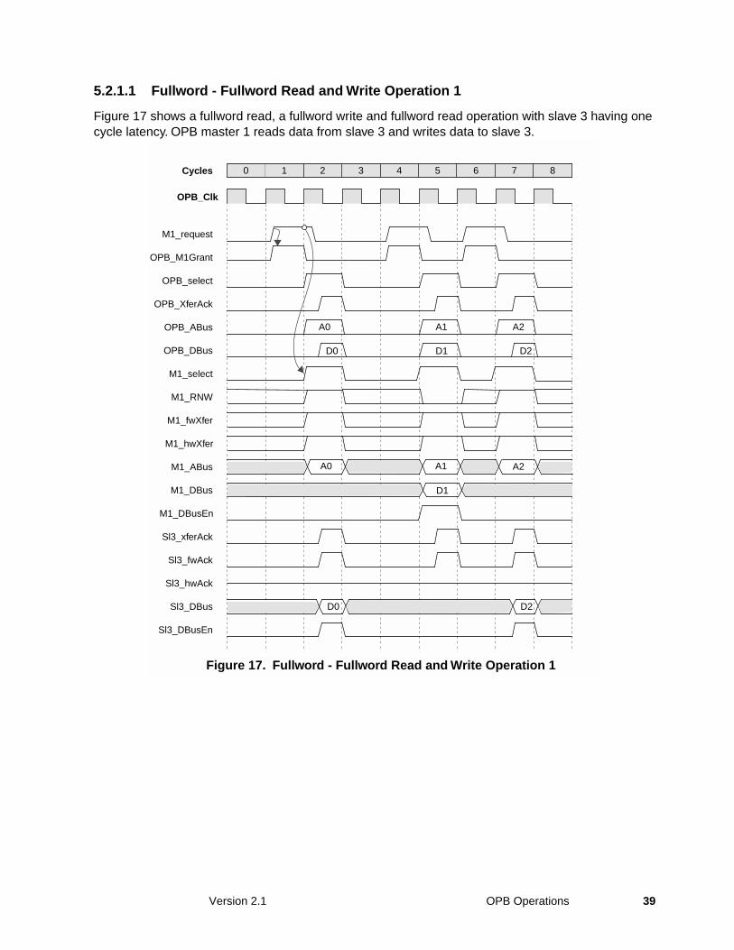
5.2.1.1 Fullword - Fullword Read and Write Operation 1
Figure 17 shows a fullword read, a fullword write and fullword read operation with slave 3 having one cycle latency. OPB master 1 reads data from slave 3 and writes data to slave 3.
OPB_Clk
OPB_select
M1_select
OPB_M1Grant
M1_request
M1_RNW
M1_fwXfer
M1_hwXfer
Figure 17. Fullword - Fullword Read and Write Operation 1
0 1 2 3 4 5 6 7 8Cycles
M1_ABus
Sl3_xferAck
Sl3_fwAck
Sl3_hwAck
Sl3_DBus
Sl3_DBusEn
OPB_XferAck
OPB_ABus
OPB_DBus
M1_DBus
M1_DBusEn
A0 A1 A2
D0 D1 D2
A0 A1 A2
D0 D2
D1
Version 2.1 OPB Operations 39

5.2.1.2 Fullword - Fullword Read and Write Operation 2
Figure 18 shows the fullword - fullword read and write operation 2 with slave 3 having two cycle latency. Master 1 reads data from slave 3 and writes data to slave 3.
OPB_Clk
OPB_select
M1_select
OPB_M1Grant
M1_request
M1_RNW
M1_fwXfer
M1_hwXfer
Figure 18. Fullword - Fullword Read and Write Operation 2
0 1 2 3 4 5 6Cycles
M1_ABus
Sl3_xferAck
Sl3_fwAck
Sl3_hwAck
Sl3_DBus
Sl3_DBusEn
OPB_xferAck
OPB_ABus
OPB_DBus
M1_DBus
M1_DBusEn
A0 A1
D0 D1
A0 A1
D1
D0
40 On-Chip Peripheral Bus Version 2.1

5.2.2 Overlapped Bus Arbitration
Figure 19 shows a more general case of OPB data transfer. In the following example, two OPB masters, master 1 and 2, require the OPB and assert requests in the same cycle. Master 1 is a fullword device, and requests a read operation from slave 3. Master 2 is a fullword device and also requests a read operation from slave 3. Slave 3 is a fullword device with a two-cycle latency. OPB Master 1 has high bus priority.
In the above example, the data transfer operation proceeds as follows:
• Master 1 and 2 assert requests in cycle 0. OPB arbiter grants to master 1 due to its higher priority by asserting OPB_M1Grant.
• Upon sampling OPB_M1Grant on the rising edge, master device 1 initiates a data transfer in cycle 1 by asserting M1_select, and negates M1_request. The OPB arbiter negates OPB_M1Grant. OPB_M2Grant is not asserted since this is not a valid arbitration cycle (bus is busy but not in final transfer cycle).
OPB_Clk
OPB_select
M1_select
OPB_M1Grant
M1_request
M1_RNW
M1_fwXfer
M1_hwXfer
0 1 2 3 4 5 6 7 8Cycles
M1_ABus
Sl3_xferAck
Sl3_fwAck
Sl3_hwAck
Sl3_DBus
Sl3_DBusEn
OPB_xferAck
OPB_ABus
OPB_DBus
M2_select
M2_RNW
M2_request
OPB_M2Grant
M2_fwXfer
M2_hwXfer
M2_ABus
A0 A1 A2
D0 D1 D2
A0 A2
A1
D0 D1 D2
Figure 19. OPB Data Transfer
Version 2.1 OPB Operations 41

• Slave 3 acknowledges in cycle 2, indicating completion of the data transfer, by asserting Sl3_xferAck. Master 1 latches data on OPB_DBus at the end of this cycle, and relinquishes control of the bus by deasserting M1_select, which also gates off all its control signals. The OPB arbiter asserts OPB_M2Grant upon the assertion of OPB_xferAck, overlapping arbitration with the data transfer.
• Master 2 then samples OPB_M2Grant at the rising edge in cycle 3, and initiates data transfer by asserting M2_select, and negates M2_request. The OPB arbiter negates OPB_M2Grant.
• Slave 3 acknowledges in cycle 4, indicating completion of the data transfer, by asserting Sl3_xferAck. Master 2 latches data on OPB_DBus at the end of this cycle, and relinquishes control of the bus by deasserting select, which also gates off all of its control signals. The OPB arbiter asserts OPB_M1Grant upon the assertion of OPB_xferAck, overlapping arbitration with the data transfer.
• Upon sampling OPB_M1Grant on the rising edge in cycle 5, master 1 initiates a data transfer by asserting M1_select, and negates M1_request. The OPB arbiter negates OPB_M1Grant.
• Finally slave 3 acknowledges in cycle 6, indicating completion of the data transfer, by asserting it’s Sl3_xferAck signal. Master 1 latches data on OPB_DBus at the end of this cycle, and relinquishes control of the bus by deasserting M1_select, which also gates off all its control signals.
Under this protocol, bus arbitration and data transfer are overlapped. This allows OPB to transfer data efficiently, avoiding dedicated bus arbitration cycles.
42 On-Chip Peripheral Bus Version 2.1

5.2.3 Continuous Bus Request
Figure 20 shows an OPB data transfer cycle when the OPB master continuously asserts its bus request signal. In the following example, OPB master 2 requests four consecutive data transfers and OPB master 1 requests one. Masters 1 and 2 are fullword devices, and both request read operations from slave device 3. Slave device 3 is a fullword device and has one cycle latency. OPB master 1 has higher bus priority than master 2. Data transfer of OPB master 2 is interrupted by OPB master 1 at cycle 3.
OPB_Clk
OPB_select
M1_select
OPB_M1Grant
M1_request
M1_RNW
Figure 20. Continuous Bus Request
0 1 2 3 4 5 6Cycles
M1_ABus
Sl3_xferAck
Sl3_DBus
Sl3_DBusEn
OPB_xferAck
OPB_ABus
OPB_DBus
M2_select
M2_RNW
M1_busLock
OPB_M2Grant
M2_ABus
M2_request
M2_busLock
OPB_busLock
A0 A1 A2 A3 A4
D0 D1 D2 D3 D4
A2
A0 A1 A3 A4
D0 D1 D2 D3 D4
Version 2.1 OPB Operations 43

5.2.4 Bus Lock Operation
The OPB provides OPB_busLock signal for continuous data transfer cycles with no interruption. Figure 21 shows a data transfer operation with the busLock signal. In this example, OPB master 1 reads data from slave 3 four times in a continuous sequence without interruption. Master 1 and 2 are fullword devices that request to read data from slave 3. Slave 3 is fullword device with 1 cycle latency. Master 1 has a higher priority than Master 2. The BusLock signal should normally be negated at the beginning of last data transfer cycle (in this case, cycle 4). This allows overlapped arbitration to occur preventing an arbitration penalty cycle.
OPB_Clk
OPB_select
M1_select
OPB_M1Grant
M1_request
M1_RNW
Figure 21. Bus Lock Data Transfer Cycle
0 1 2 3 4 5 6Cycles
M1_ABus
Sl3_xferAck
Sl3_DBus
Sl3_DBusEn
OPB_xferAck
OPB_ABus
OPB_DBus
M2_select
M2_RNW
M1_busLock
OPB_M2Grant
M2_ABus
M2_request
M2_busLock
OPB_busLock
A0 A1 A2 A3 A4
D0 D1 D2 D3 D4
A0 A1 A2 A3
A4
D0 D1 D2 D3 D4
44 On-Chip Peripheral Bus Version 2.1

Figure 22 demonstrates the case in which an extra arbitration cycle is necessary due to busLock not being deasserted during the last data transfer cycle. Device conditions are the same as for the previous figure. In the following example, master 1 asserts busLock signal at the start of its data transfer and continues to assert busLock through the last transfer cycle. A grant is generated at cycle 4 if the master asserts request. Even if the master does not assert request, there will be no arbitration cycle there, due to busLock being asserted, which prevents the normal OPB overlapped arbitration. The OPB requires one additional cycle for arbitration, to grant master 2 at cycle 5.
OPB_Clk
OPB_select
M1_select
OPB_M1Grant
M1_request
M1_RNW
Figure 22. Bus Lock Signal Penalty Case
0 1 2 3 4 5 6 7Cycles
M1_ABus
Sl3_xferAck
Sl3_DBus
Sl3_DBusEn
OPB_xferAck
OPB_ABus
OPB_DBus
M2_select
M2_RNW
M1_busLock
OPB_M2Grant
M2_ABus
M2_request
M2_busLock
OPB_busLock
arbi
trat
ion
cycl
eA0 A1 A2 A3 A4
D0 D1 D2 D3 D4
A0 A1 A2 A3
A4
D0 D1 D2 D3 D4
Version 2.1 OPB Operations 45

5.2.5 Sequential Address Signal Operation
The OPB provides the seqAddr signal for multiple data transfers to sequential addresses to the same slave. This signal is asserted by the OPB master to indicate that the transfer being performed will be followed with a transfer to the next sequential address. This signal is always used in conjuction with the bus arbitration lock in order to guarantee that there are no intervening bus operations that might occur to non-sequential addresses. Master 1 will read data from slave 3 four times, using SeqAddr and busLock signals. Slave 3 normally has a 2 cycle latency, but can achieve 1 cycle latency in “burst mode” by avoiding subsequent address decode cycles. Data transfer requires only 5 cycles (2+1+1+1) even if this slave normally requires two cycles to access and provide data. Without OPB_seqAddr, 8 cycles would be required.
OPB_Clk
OPB_select
M1_select
M1_request
M1_RNW
Figure 23. Sequential Address Signal Operation
0 1 2 3 4 5 6Cycles
M1_ABus
Sl3_xferAck
Sl3_DBus
Sl3_DBusEn
OPB_xferAck
OPB_ABus
OPB_DBus
M1_busLock
OPB_busLock
OPB_seqAddr
OPB_M1Grant
M1_seqAddr
M1_fwXfer
M1_hwXfer
Sl3_fwAck
Sl3_hwAck
A0 A0+4 A0+8 A0+C
D0 D1 D2 D3
A0 A0+4 A0+CA0+8
D0 D1 D2 D3
46 On-Chip Peripheral Bus Version 2.1

5.2.6 Slave Re-try Operation
To alleviate deadlock scenarios on the bus, the OPB provides the Sln_retry signal. The retry signal forces the requesting master to abandon a pending data transfer, and allow the OPB arbiter to rearbitrate the bus.
The retry signal is asserted by an OPB bus slave to indicate that there exists a condition which precludes the slave from performing the indicated bus operation at this time.
A bus slave will assert the Sln_retry signal instead of the Sln_xferAck signal when a situation requiring it is detected. It will remain asserted until the bus slave becomes deselected as a result of the ‘select’ signal being deasserted.
The bus master will respond to this signal by immediately terminating the transfer in progress and relinquishing control of the bus. This is accomplished by the master deasserting Mn_select and, if asserted, OPB_busLock in the cycle following the detection of the OPB_retry signal. The bus master requesting the transfer is also required to deassert Mn_request for one cycle following the detection of OPB_retry to allow for resolution of the deadlock. Following this one-cycle request back-off the master may then proceed to request the transfer again, or request another transfer.
The OPB arbiter will re-arbitrate the bus in the cycle in which Mn_select and Mn_busLock are deasserted by the master. In this cycle, the master that was just retried is required to drop his request and this gives the slave which retried the operation a chance to access the OPB in order to resolve the deadlock condition.
The retry signal, and the requirement that retried masters terminate their transfer and back off requests for one cycle, is insufficient to guarantee that all deadlock scenarios will be alleviated. Depending on the number and type of master devices connected to the OPB, and their relative arbitration priorities, it is possible that deadlock conditions will arise which the retry will not solve. It does, however, provide master devices on the OPB with sufficient information to detect a deadlock condition, and to take appropriate actions to resolve it.
System designers should also be aware that a retry operation can break a locked series of transfers, due to the requirement that the master deassert Mn_busLock for one cycle if it is active. This is necessary to allow for an arbitration cycle on the OPB. This raises the possibility, however, that a retry operation could interrupt an atomic transfer, and a different master could win the next arbitration cycle. In this case, nothing prevents the new master from accessing data to/from the same address as the locked transfers.
In the following example, OPB master 2 and slave 2 are the same unit, a bridge to an external bus. That bus has initiated a write to OPB slave 3, to which it is committed and which is using all its internal resources. OPB master 1 has a higher priority on the OPB, and requests a read from slave 2. Slave 2, however, cannot respond to the read request until it performs its write to slave 3. This condition is a deadlock. It would be inappropriate for slave 2 to merely ignore master 1’s request and cause a time-out, or to respond with Sl2_errAck, since this is not an error condition. Slave 2 thus issues Sl2_retry. This causes master 1 to terminate the current cycle by removing its select, and back off the bus for one cycle by removing its request. This causes an arbitration cycle on the OPB. The master side of the external bus bridge, master 2, then wins arbitration, and performs a write to slave 3. Master 1 then resumes its request, receives a grant, and issues its read to slave 2, which is now free to respond.
Version 2.1 OPB Operations 47

Figure 24 shows retry signal operation.
OPB_Clk
OPB_select
M1_select
OPB_M1Grant
M1_request
M1_RNW
Figure 24. Retry Signal Operation
0 1 2 3 4 5 6 7Cycles
Sl3_xferAck
Sl2_xferAck
Sl3_retry
OPB_xferAck
OPB_ABus
OPB_DBus
M2_select
M2_RNW
OPB_M2Grant
M2_request
M1_fwXfer
M1_hwXfer
M2_fwXfer
M2_hwXfer
Sl2_retry
arbi
trat
ion
cycl
e
48 On-Chip Peripheral Bus Version 2.1

5.2.7 OPB Master Abort
Figure 25 shows an OPB master abort cycle. The OPB master first asserts its request signal. The OPB arbiter asserts the master’s grant signal. The requesting OPB master device then assumes OPB ownership by asserting its select signal in the cycle following that in which it samples its grant at the rising edge of OPB Clock. The master subsequently determines that it no longer wishes to perform the current transfer and deasserts its select signal. This condition forces the slave to abort the transfer and to return to its idle condition. Note that the slave may leave Sln_TouSup asserted in the clock following select deassertion. (cycle 5).
OPB_Clk
OPB_select
M1_select
OPB_M1Grant
M1_request
M1_RNW
M1_fwXfer
M1_hwXfer
Figure 25. OPB Master Abort
1 2 3 4 5 6Cycles
M1_ABus
Sl2_xferAck
Sl2_fwAck
Sl2_hwAck
Sl2_DBus
valid address
Sl2_ToutSup
Version 2.1 OPB Operations 49

5.2.8 Bus TimeOut Error
All slave devices on the OPB must respond to OPB_select within 16 cycles from the assertion of OPB_select by asserting Sln_xferAck or Sln_retry signals. If OPB_xferAck or OPB_retry signal is not asserted, then the OPB arbiter will assert OPB_timeout signal in the 16th cycle. A slave device which requires more than 16 cycles to complete its transfer may inhibit the timeout counter by asserting the Sln_ToutSup signal.
The OPB_timeout signal is driven from the OPB arbiter to each OPB master attached to the OPB. This signal is used to indicate to the OPB master that a Timeout error has occurred and that the master should terminate the transfer. The master must drop its select signal in the cycle following the cycle in which the OPB_timeout signal is detected as being active.
If the bus is not locked, the arbiter will re-arbitrate in the cycle in which the select is deactivated and will proceed to grant a new master of the bus. If the bus is locked, the master is still required to deactivate the select signal for one cycle and then may proceed in the following cycle to re-activate the select signal to perform another transfer.
Note that specifying the timeout counter as fixed at sixteen cycles requires that a slave device respond within 16 cycles by either activating its Sln_xferAck or Sln_retry signal or by activating the Sln_ToutSup signal.
The slave may assert Sln_ToutSup any time up to and including within the 16th cycle following the assertion of OPB_select. When OPB_ToutSup is asserted, the OPB arbiter will suppress OPB_timeout signal and suspend the timeout counter in the OPB arbiter.
If OPB_xferAck and OPB_timeout are active in the same cycle (i.e., the slave responds in the 16th cycle following OPB_select), the master should accept OPB_xferAck, completing the transfer, and ignore the OPB_timeout signal.
If OPB_retry and OPB_timeout are active in the same cycle (i.e., the slave responds in the 16th cycle following OPB_select), the master should accept OPB_retry and ignore OPB_timeout. In this case the effect will be similar, as both signals require the master to relinquish control of the OPB by removing its select signal in the following cycle. OPB_retry, however, also requires that the master remove its request in the following cycle, and may initiate other, system-dependant activity on the part of the master to alleviate system deadlock.
50 On-Chip Peripheral Bus Version 2.1

5.2.8.1 OPB Bus Timeout Error Condition
Figure 26 shows an OPB timeout error. Master 1 and 2, and slave 3 and 4 are fullword devices. Master 1 will read data from slave 3, master 2 will read data from slave 4. In this case master 1 has higher priority than master 2.
OPB slave 3 does not respond to the OPB master 1’s request within the 16 cycles. The OPB arbiter asserts OPB_timeout. Master 1 then terminates this data transfer by negating M1_select in clock 17.
D1
OPB_Clk
OPB_select
M1_select
OPB_M1Grant
M1_request
Figure 26. Bus Timeout Error Condition
0 1 15 16 17 18 19Cycles
M1_ABus
Sl3_xferAck
Sl3_DBus
Sl3_DBusEn
OPB_xferAck
OPB_ABus
OPB_DBus
M2_select
OPB_M2Grant
M2_ABus
M2_request
OPB_timeout
Sl3_toutSup
Sl4_xferAck
Sl4_toutSup
Sl4_DBus
Sl4_DBusEn
A0 A1
D1
A0
A1
Version 2.1 OPB Operations 51

5.2.8.2 OPB Timeout Error Suppression
Figure 27 shows an OPB slave suppressing a TimeOut error with the ToutSup signal. Master 1 and 2, and slave 3 and 4 are fullword devices. Master 1 will read data from slave 3, master 2 will read data from slave 4. In this case master 1 has higher priority than master 2. The OPB master 1 still does not have a response from the OPB slave 3 by the TimeOut cycle, but slave device 3 asserts its ToutSup Signal. The OPB slave suppresses OPB_timeout from the arbiter, and master 1 waits for a response from the slave, after which OPB transactions proceed normally.
OPB_Clk
OPB_select
M1_select
OPB_M1Grant
M1_request
Figure 27. Timeout Error Suppression
0 1 16 16+X 16+X+1 16+X+2 16+X+3Cycles
M1_ABus
Sl3_xferAck
Sl3_DBus
Sl3_DBusEn
OPB_xferAck
OPB_ABus
OPB_DBus
M2_select
OPB_M2Grant
M2_ABus
M2_request
OPB_timeout
Sl3_toutSup
Sl4_xferAck
Sl4_toutSup
Sl4_DBus
Sl4_DBusEn
A0 A1
D0 D1
A1
D0
D1
52 On-Chip Peripheral Bus Version 2.1

5.3 Dynamic Bus Sizing
Dynamic bus sizing is a feature of the on-chip peripheral bus that permits devices having different data bus widths to interoperate. Dynamic bus sizing is performed on a transfer by transfer basis. Bus sizing operation is controlled by the following six signals on the bus:
• Halfword transfer
• Fullword transfer
• Doubleword transfer
• Halfword acknowledge
• Fullword acknowledge
• Doubleword acknowledge
When the OPB master performs an operation that is wider than the selected OPB slave, the master must split the operation into two or more smaller transfers. These are referred to as conversion cycles.
5.3.1 Data Alignment
Figure 28 shows attachment of bus devices of varying widths. All devices are attached “Left Justified” to the bus, that is, byte devices are attached to bits 0:7, halfword devices are attached to bits 0:15, fullword devices are attached to bits 0:31, and doubleword devices are attached to bits 0:63.
D00:D07
D08:D15
D16:D23
D24:D31
Ful
lwor
d D
evic
e
Hal
fwor
d D
evic
e
Figure 28. Attachment Of Bus Devices Of Varying Width
Byt
e D
evic
e
D32:D39
D40:D47
D48:D55
D56:D63
Dou
blew
ord
Dev
ice
Version 2.1 OPB Operations 53

Byte, halfword, fullword, and doubleword transfers to a doubleword device are transferred memory aligned using all 64-bits of the data bus. Byte, halfword, and fullword transfers to a word device are transferred memory aligned using the high order 32-bits of the data bus. Byte and halfword transfers to a halfword device are transferred memory aligned using the high order 16-bits of the data bus. Byte transfers to byte devices are transferred using the high order byte of the bus. Dynamic bus sizing occurs in three different situations.
1. When a master makes a request greater than the data width of the slave.
2. When a master makes a request which is smaller than both the master and slave data widths.
3. When a slave data width is greater than the master.
5.3.2 Master Transfer and Slave Sizing
Master transfer size is indicated by the doubleword, fullword, and halfword transfer signals. Doubleword transfers are indicated by doubleword, fullword, and halfword transfers being asserted. Fullword transfers are indicated by only fullword and halfword transfer signals being asserted. Halfword transfers are indicated by only halfword transfer being asserted. Byte transfers are indicated by none of the transfer size signals being asserted. All of other combinations of these signals are reserved. Only 64-bit Masters can request doubleword transfers. Both 64-bit and 32-bit masters can assert all other size transfers.
Slave size is indicated by the doubleword, fullword, and halfword acknowledge signals. Doubleword slaves assert doubleword and fullword acknowledge. Fullword slaves assert only fullword acknowledge, halfword slaves assert only halfword acknowledge, and byte slaves assert none of the slave size acknowledge signals. All of other combinations of these signals are reserved. It is permissible for an OPB slave to function as different types of slaves on different transfers
5.3.3 Write Data Mirroring and Read Data Steering
32-bit and 64-bit masters are supported on the OPB. Each may be connected to either a 32-bit or 64-bit OPB implementation. During write cycles masters are required to “mirror” write data to byte lanes onto which smaller width slaves may be connected. During read cycles byte, halfword, and fullword slaves provide read data on the byte lanes which they are connected to. In the case of a 64-bit OPB implementation being written to by a 32-bit master the master must mirror Mn_DBus(0:31) onto Mn_DBus(32:63) when Mn_Abus(29) is a one. Both Mn_DBusEn and Mn_DBusEn32_63 must also be asserted. This allows 64-bit slaves to always latch data directly from the 64-bit bus. In the case of a 64-bit slave being read from the slave must “steer” read data to the high order byte lanes of the OPB data bus when OPB_Abus(29) is high. This is to support reads by a 32-bit master.
The following tables illustrate the master and slave requirements to correctly perform dynamic bus sizing. Table 9, “32-bit Master Write Data Mirroring,” on p. 55 and Table 10, “64-bit Master Write Data Mirroring,” on p. 56 show master write data mirroring to support smaller slaves. Table 11, “64-bit Slave Read Steering,” on p. 57 shows read data steering by a 64-bit slave to support 32-bit masters.Table 12, “Fullword and Halfword Conversion Cycle Sequences,” on p. 58 and Table 13, “Doubleword Conversion Cycle Sequences,” on p. 59 illustrate the resultant conversion cycles for all type of the transfers.
Note: When a master or slave has either Mn_DBusEn, Mn_DBusEn32_63, Sln_DBusEn, or Sln_DBusEn32_63 asserted respectively it is recommended that unused byte lanes be
54 On-Chip Peripheral Bus Version 2.1

optionally driven with zeroes, 8’b0, in order to conserve power consumption by not switching those data bus nets. Unused byte lanes in the following tables are indicated by a “blank box”.
5.3.3.1 32-bit Master Write Data Mirroring
The data mirroring for 32-bit master write cycles is shown in Table 9. A 32-bit master is responsible for mirroring the write data to all smaller width slaves. Since the master does not know what size the slave is until OPB_xferAck is asserted it must always mirror data to the byte lanes of smaller width devices when OPB_ABus(30) or OPB_ABus(31) are one. Mirrored bytes are in bold font.
Table 9. 32-bit Master Write Data Mirroring
32-bit Data Bus
ABus (28:31)
TransferSize
Dbus0:7
byte0
Dbus 8:15
byte1
Dbus 16:23byte2
Dbus 24:31byte3
00 fullword byte0 byte1 byte2 byte3
00 halfword byte0 byte1
10 halfword byte2 byte3 byte2 byte3
00 byte byte0
01 byte byte1 byte1
10 byte byte2 byte2
11 byte byte3 byte3 byte3
Version 2.1 OPB Operations 55

5.3.3.2 64-bit Master Write Data Mirroring
The data mirroring for 64-bit master write cycles is shown in Table 10. A 64-bit master is responsible for mirroring the write data to all smaller width slaves. Since the master does not know what size the slave is until OPB_xferAck is asserted it must always mirror data to the byte lanes of smaller width devices when OPB_ABus(29) or OPB_ABus(30) or OPB_ABus(31) are one. Mirrored bytes are in bold font.
Table 10. 64-bit Master Write Data Mirroring
64-bit Data Bus
ABus (29:31)
TransferSize
Dbus0:7
byte0
Dbus 8:15
byte1
Dbus 16:23byte2
Dbus 24:31byte3
Dbus 32:39byte4
Dbus40:47byte5
Dbus48:55byte6
Dbus56:63byte7
000 doubleword byte0 byte1 byte2 byte3 byte4 byte5 byte6 byte7
000 fullword byte0 byte1 byte2 byte3
100 fullword byte4 byte5 byte6 byte7 byte4 byte5 byte6 byte7
000 halfword byte0 byte1
010 halfword byte2 byte3 byte2 byte3
100 halfword byte4 byte5 byte4 byte5
110 halfword byte6 byte7 byte6 byte7 byte6 byte7
000 byte byte0
001 byte byte1 byte1
010 byte byte2 byte2
011 byte byte3 byte3 byte3
100 byte byte4 byte4
101 byte byte5 byte5 byte5
110 byte byte6 byte6 byte6
111 byte byte7 byte7 byte7 byte7
56 On-Chip Peripheral Bus Version 2.1

5.3.3.3 64-bit Slave Read Data Steering
The data steering for 64-bit slave read cycles is shown in Table 11. A 64-bit slave is responsible for steering the data during read cycles when ABus (29) is a one to support accesses by 32-bit masters. To conserve power consumption it is recommended that Sl_DBusEn32_63 not be asserted by the slave when no data is being transferred on byte lanes 4-7.
Table 11. 64-bit Slave Read Steering
64-bit Data Bus
ABus(29:31)
Transfer Size
Dbus0:7
byte0
Dbus8:15
byte1
Dbus16:23byte2
Dbus24:31byte3
Dbus32:39byte4
Dbus40:47byte5
Dbus48:55byte6
Dbus56:63byte7
000 doubleword byte0 byte1 byte2 byte3 byte4 byte5 byte6 byte7
000 fullword byte0 byte1 byte2 byte3
100 fullword byte4 byte5 byte6 byte7 byte4 byte5 byte6 byte7
000 halfword byte0 byte1
010 halfword byte2 byte3
100 halfword byte4 byte5 byte4 byte5
110 halfword byte6 byte7 byte6 byte7
000 byte byte0
001 byte byte1
010 byte byte2
011 byte byte3
100 byte byte4 byte4
101 byte byte5 byte5
110 byte byte6 byte6
111 byte byte7 byte7
Version 2.1 OPB Operations 57

5.3.4 Conversion Cycles
Conversions cycles are required when a master requests a transfer that is wider than the width of the slave. This requires the master perform additional transfers, or conversions, to complete the original request.
5.3.4.1 Fullword and Halfword Conversion Cycles
Conversion cycles are required in the case of a fullword transfer to halfword and byte slaves or a halfword transfer to a byte slave. Table 12 shows the initial and next transfer(s) driven by the master during conversion cycles.
Table 12. Fullword and Halfword Conversion Cycle Sequences
Transfer ABus(30:31)
Transfer Request
Slave Response
initial 00 fullword halfword Ack
conversion 10 halfword halfword Ack
initial 00 fullword byte Ack
conversion 01 byte byte Ack
conversion 10 halfword byte Ack
conversion 11 byte byte Ack
initial 00 halfword byte Ack
conversion 01 byte byte Ack
initial 10 halfword byte Ack
conversion 11 byte byte Ack
58 On-Chip Peripheral Bus Version 2.1

5.3.4.2 Doubleword Conversion Cycles
Conversion cycles are required in the case of a doubleword transfer request to a fullword, halfword, or byte slave. Table 13 shows the initial and next transfer(s) driven by the master during a conversion cycles.
5.3.5 Data Transfer with Dynamic Bus Sizing Waveform Examples
The sections that follow demonstrate representative combinations of device widths which give rise to data transfer cycles utilizing dynamic bus sizing.
5.3.5.1 Fullword - Halfword Read and Write Operation
Figure 29 shows fullword - halfword read and write operation. Master 1 which is a fullword device will read and write data to slave 3. Slave 3 is a halfword device and has one cycle latency. Note that in
Table 13. Doubleword Conversion Cycle Sequences
Transfer ABus(29:31)
Transfer Request
Slave Response
initial 000 doubleword fullword Ack
conversion 100 fullword fullword Ack
initial 000 doubleword halfword Ack
conversion 010 halfword halfword Ack
conversion 100 fullword halfword Ack
conversion 110 halfword halfword Ack
initial 000 doubleword byte Ack
conversion 001 byte byte Ack
conversion 010 halfword byte Ack
conversion 011 byte byte Ack
conversion 100 fullword byte Ack
conversion 101 byte byte Ack
conversion 110 halfword byte Ack
conversion 111 byte byte Ack
Version 2.1 OPB Operations 59

cycle 7, master device 1 will drive the data bus with the second halfword. It will be replicated across both halfword positions, so the full 32 bit data bus will be driven with valid data.
OPB_Clk
OPB_select
M1_select
OPB_M1Grant
M1_request
M1_RNW
Figure 29. Fullword - Halfword Read and Write Operation
0 1 2 3 4 5 6 7 8Cycles
M1_ABus
Sl3_xferAck
Sl3_DBus
Sl3_DBusEn
OPB_xferAck
OPB_ABus
OPB_DBus
M1_busLock
OPB_busLock
M1_fwXfer
M1_hwXfer
M1_DBus
M1_DBusEn
Sl3_fwAck
Sl3_hwAck
transfer attempted by master
bus width ack’ed by slave
FW HW FW HW
HW HW HW HW
00 10 00 10
0:150:310:150:15
00 10 00 10
0:150:31
0:15 0:15
60 On-Chip Peripheral Bus Version 2.1

5.3.5.2 Fullword - Byte Read Operation
Figure 30 shows fullword - byte read operation. Master 1 is a fullword device, slave 2 is a byte device with 1 cycle latency. Master 1 requests to read fullword data from slave 2. Master 1 generates the three additional cycles (3-5) to comply with the dynamic bus sizing requirement. Note that each of these transfers is separately arbitrated, and it is possible that the sequence could be interrupted by other, higher priority, master devices.
OPB_Clk
OPB_select
M1_select
OPB_M1Grant
M1_request
M1_RNW
Figure 30. Fullword - Byte Read Operation
0 1 2 3 4 5 6Cycles
M1_fwXfer
Sl2_XferAck
Sl2_DBus
Sl2_DBusEn
OPB_XferAck
OPB_ABus
OPB_DBus
M1_hwXfer
M1_ABus
M1_busLock
OPB_busLock
Sl2_fwAck
Sl2_hwAck
transfer attempted by master
bus width ack’ed by slave
FW
BYTE
BYTE
BYTE
HW BYTE
BYTE BYTE
00 01 10 11
B0 B1 B2 B3
00 01 1110
B3B2B1B0
Version 2.1 OPB Operations 61

5.3.5.3 Doubleword - Fullword Read and Write Operation
Figure 31 shows doubleword - fullword read and write operation. Master 1 which is a doubleword device will read and write data to slave 3. Slave 3 is a fullword device and has one cycle latency. Note that in cycle 7, master device 1 will drive the data bus with the second fullword. It will be replicated across both upper and lower fullword positions, so the full 64-bit data bus will be driven with valid data.
OPB_Clk
OPB_select
M1_select
OPB_M1Grant
M1_request
M1_RNW
Figure 31. Doubleword - Fullword Read and Write Operation
0 1 2 3 4 5 6 7 8Cycles
M1_ABus(29:31)
Sl3_xferAck
Sl3_DBus
Sl3_DBusEn
OPB_xferAck
OPB_ABus(29:31)
OPB_DBus
M1_busLock
OPB_busLock
M1_hwXfer
1_DBus(0:31)
M1_DBusEn
Sl3_dwAck
Sl3_fwAck
transfer attempted by master
bus width ack’ed by slave
DW FW DW FW
FW FW FW FW
000 100 000 100
0:630:630:310:31
000 100 000 100
32:630:31
0:31 0:31
M1_dwXfer
M1_fwXfer
Sl3_hwAck
M1_DBus
M1_DBusEn32_63
32:6332:63
62 On-Chip Peripheral Bus Version 2.1

5.3.5.4 Doubleword - Halfword Read Operation
Figure 32 shows doubleword - halfword read operation. Master 1 is doubleword device, slave 2 is halfword device with 1 cycle latency. Master 1 requests a doubleword read from slave 2. Master 1 generates the three additional cycles to comply with the dynamic bus sizing requirement. Note that each of these transfers is separately arbitrated, and it is possible that the sequence could be interrupted by other, higher priority, master devices.
OPB_Clk
OPB_select
M1_select
OPB_M1Grant
M1_request
M1_RNW
Figure 32. Doubleword - Halfword Read Operation
0 1 2 3 4 5 6Cycles
Sl2_XferAck
Sl2_DBus(0:15)
OPB_XferAck
OPB_ABus(29:31)
OPB_DBus
M1_hwXfer
M1_ABus
M1_busLock
OPB_busLock
Sl2_dwAck
Sl2_fwAck
transfer attempted by master
bus width ack’ed by slave
DW
HW
HW
HW
FW HW
HW HW
HW0 HW1 HW2 HW3
000 010 110100
HW3HW2HW1HW0
M1_dwXfer
M1_fwXfer
7
000 010 100 110
Sl2_hwAck
Sl2_DBusEn
Version 2.1 OPB Operations 63

5.3.5.5 Doubleword - Byte Write Operation
Figure 33 shows doubleword - byte write operation. Master 1 is doubleword device, slave 1 is byte device with 1 cycle latency. Master 1 requests a doubleword write to slave 1. Master 1 generates the seven additional cycles to comply with the dynamic bus sizing requirement. Note that in clock 2, 7, and 10 Master 1 deasserts its request because it is not sure what size the slave will respond as. In other words whether or not the slave will take the full write on not.
OPB_Clk
OPB_select
OPB_M1Grant
M1_request
M1_RNW
Figure 33. Doubleword - Byte Write Operation
1 2 3 4 5 6 7 8 9Cycles
OPB_xferAck
OPB_ABus(29:31)
M1_fwXfer
M1_hwXfer
M1_DBusEn
OPB_dwAck
10
000 001 010 100 101
11 12 13
M1_DBusEn32_63
011 110 111
M1_select
M1_dwXfer
OPB_DBus(0:31) B0-B3 B1-B3 B2-B3 B4-B7 B5-B7B3 B6-B7 B7
OPB_DBus(32:63) B4-B7 B4-B7 B5-B7 B6-B7 B7
M1_DBus(0:31) B0-B3 B1-B3 B2-B3 B4-B7 B5-B7B3 B6-B7 B7
M1_DBus(32:63) B4-B7 B4-B7 B5-B7 B6-B7 B7
Sl1_xferAck
OPB_fwAck
OPB_hwAck
64 On-Chip Peripheral Bus Version 2.1

5.3.5.6 Dynamic Bus Sizing and Overlapped Arbitration
Figure 34 shows a representative sequence of OPB data transfers, where one master performs dynamic bus sizing and the other does not. Arbitration is overlapped between the two masters. In this case, OPB master 1 will read and write data to OPB slave 3 and OPB master 2 will read data from OPB slave 4. OPB master 1 and 2, and slave 3, are fullword devices and slave 4 is a halfword device.
OPB_Clk
OPB_select
M1_select
OPB_M1Grant
M1_request
M1_RNW
Figure 34. Overlapped Arbitration
1 2 3 4 5 6 7 8 9Cycles
M1_ABus
Sl3_xferAck
Sl3_DBus
Sl3_DBusEn
OPB_xferAck
OPB_ABus
OPB_DBus
M2_select
M2_RNW
OPB_M2Grant
M2_ABus
M2_request
M1_fwXfer
M1_hwXfer
M1_DBus
M1_DBusEn
M2_fwXfer
M2_hwXfer
Sl3_fwAck
Sl3_hwAck
Sl4_xferAck
Sl4_DBus
Sl4_fwAck
Sl4_hwAck
10
M1-A0 M2-00 M1-A1 M2-10 M2-00 M2-10
D0 0:15 D1 0:15 0:31 0:15
A0 A1
D1
00 10 00 10
D0
0:15 0:15
Version 2.1 OPB Operations 65

5.3.5.7 Locked Dynamic Bus Sizing With Interruption
Figure 35 shows a case where a master asserts busLock to lock the bus for the duration of the dynamic bus sizing sequence.The data transfer, including dynamic bus sizing, proceeds as in the previous case. However, the master asserted busLock. This precludes another master (M2) of higher priority from interrupting the sequence in cycle 3. Master 1 deasserts busLock in cycle 5, the last of its data transfer cycles. This allows the OPB to arbitrate in cycle 5, granting the bus to master 2, which assumes ownership of the bus by asserting M2_select in cycle 6 (the full details of master 2’s data transfer omitted).
Even using busLock in the manner described below, a master device cannot guarantee an uninterrupted dynamic bus sizing operation. If another, higher priority, master asserts a request during the first access (a valid arbitration cycle), it could obtain (and lock) the bus. The first master device will not know the bus width of the addressed slave until it receives acknowledge, and thus only then will it realize that additional data transfer cycles are necessary.
OPB masters that require uninterrupted data transfer, including dynamic bus sizing cycles, may achieve this by asserting busLock for every cycle, even for nominally single-cycle fullword and halfword transfers. This approach defeats the overlapped arbitration capability of the OPB, and reduces overall bandwidth, as it requires idle cycles on the bus for arbitration for those cases where slaves are able to respond to the transfer size requested.
66 On-Chip Peripheral Bus Version 2.1

OPB_Clk
OPB_select
M1_select
OPB_M1Grant
M1_request
M1_RNW
Figure 35. Dynamic Bus Sizing With BusLock Signal
0 1 2 3 4 5 6 7Cycles
M1_ABus
Sl2_xferAck
Sl2_DBus
Sl2_DBusEn
OPB_xferAck
OPB_ABus
OPB_DBus
M2_select
Sl2_fwAck
M1_busLock
OPB_M2Grant
Sl2_hwAck
M2_request
OPB_busLock
M1_fwXfer
M1_hwXfer
transfer attempted by master FW BYTE HW BYTE
bus width ack’ed by slave BYTE BYTE BYTE BYTE
00 01 10 11
0:7 0:7 0:7 0:7
00 01 1010
0:7 0:7 0:7 0:7
Version 2.1 OPB Operations 67

5.3.5.8 Locked Dynamic Bus Sizing With No Interruption
Figure 36 shows locked dynamic bus sizing with no interruption. In this case, master 1 and 2 are fullword devices, slave 3 is halfword device and slave 4 is fullword device. Both slave devices have 1 cycle latency. Master 1 requests to read data from slave 3 and master 2 requests to read data from slave 4.
In this case, the data transfers at cycles 2 and 6 are generated by master 1 for dynamic bus sizing (fullword reads from halfword slave device). When dynamic bus sizing is required, this procedure is effective, as it provides dynamic bus sizing without interruption and the following data transfer can take advantage of overlapped bus arbitration.
However, if dynamic bus sizing is not required, this procedure requires a dedicated arbitration cycle for the next data transfer. This is the case for master 2, which asserted busLock, but did not require dynamic bus sizing cycles. The OPB arbiter generates a grant (if master 2 is requesting) at cycles 3 and 7. Whether or not master 2 requests and receives grants in these cycles, the fact that it has locked the bus prevents arbitration cycles there. The OPB arbiter thus uses cycles 4 and 8 for bus arbitration.
The system designer implementing master devices on the OPB will need to consider which approach to dynamic bus sizing is appropriate for each application.
Figure 37 and Figure 38 demonstrate representative data transfer cycles utilizing dynamic bus sizing, where BusLock is asserted immediately (i.e., the master device is “aware” of the bus width of the addressed slaves, anticipates the need for dynamic bus sizing, and wishes to complete the entire data transfer without interruption).
68 On-Chip Peripheral Bus Version 2.1

OPB_Clk
OPB_busLock
OPB_xferAck
M2_request
M1_request
OPB_ABus
Figure 36. Dynamic Bus Sizing Without Interruption
0 1 2 3 4 5 6 7 8Cycles
M1_fwXfer
Sl3_xferAck
Sl3_DBus
Sl3_DBusEn
OPB_M1Grant
OPB_M2Grant
OPB_select
M2_select
M2_busLock
M2_ABus
M1_busLock
OPB_DBus
M1_select
M1_hwXfer
M1_ABus
M2_fwXfer
M2_hwXfer
Sl3_fwAck
Sl3_hwAck
Sl4_xferAck
Sl4_DBus
Sl4_fwAck
Sl4_hwAck
9
Sl4_DBusEn
Transfer attempted by master FW FWHW FW
Bus width ack’ed by slave HW FW HWHW
HW
HW
FW
FW
00 10 00 00 10 00
0:15 0:15 0:310:150:15 0:31
00 10 00 10
00 00
0:150:15 0:150:15
0:31 0:31
arbi
trat
ion
cycl
e
arbi
trat
ion
cycl
e
arbi
trat
ion
cycl
e
Version 2.1 OPB Operations 69

5.3.5.9 Fullword - Byte Read and Write Operation
Figure 37 shows fullword - byte read and write operation with BusLock. Master 1 which is a fullword device will read and write data to slave 2. Slave 2 is a byte device with one cycle latency.
OPB_Clk
OPB_select
M1_select
PB_M1Grant
M1_request
M1_RNW
Figure 37. Fullword - Byte, Read and Write Operation
0 1 2 3 4 5 6 7 8Cycles
M1_ABus
Sl2_xferAck
Sl2_DBus
Sl2_DBusEn
OPB_xferAck
OPB_ABus
OPB_DBus
OPB_busLock
M1_busLock
M1_fwXfer
M1_hwXfer
M1_DBus
M1_DBusEn
Sl2_fwAck
Sl2_hwAck
9
transfer attempted by master
bus width ack’ed by slave
FW
BYTE
HW FW HWBYTE BYTE
BYTEBYTEBYTE BYTE
BYTE
BYTE BYTE
BYTE
BYTE
00 01 10 11 00 01 10 11
0:70:150:70:310:70:7 0:7 0:7
00 01 10 11 00 01 10 11
0:70:7 0:150:31
0:70:70:70:7
70 On-Chip Peripheral Bus Version 2.1

5.3.5.10 Halfword - Byte, Read and Write Operation
Figure 38 shows halfword - byte read and write operation with BusLock. Master 1 which is a halfword device will read and write data to slave 2. Slave 2 is a byte device with one cycle latency. The master device anticipates the bus width of the slave, and asserts BusLock immediately for guaranteed uninterrupted access to the bus for the duration of the data transfer.
The OPB bus architecture includes optional support for byte enable transfers. While dynamic bus sizing works adequately in most applications byte enables offer advantages from a performance perspective with a moderate increase in complexity. OPB systems can be implemented consisting of all 64-bit masters and 64-bit slaves being byte enable capable. This would eliminate the need for any dynamic bus sizing and its associated complexity however this would come at the price of not being able to use legacy devices. The following outlines the operation of byte enables on the OPB and their seamless cohabitation with devices that do not support byte enables and rely on dynamic bus sizing instead.
OPB_Clk
OPB_select
M1_select
OPB_M1Grant
M1_request
M1_RNW
Figure 38. Halfword - Byte, Read and Write Operation
0 1 2 3 4 5Cycles
M1_ABus
Sl3_xferAck
Sl2_DBus
Sl2_DBusEn
OPB_xferAck
OPB_ABus
OPB_DBus
M1_busLock
OPB_busLock
M1_fwXfer
M1_hwXfer
M1_DBus
M1_DBusEn
Sl2_hwAck
Sl2_fwAck
transfer attempted by master
bus width ack’ed by slave
HW
BYTE
HWBYTE BYTE
BYTEBYTEBYTE
0 1 0 1
0:7 0:7 0:15 0:7
0 1 0 1
0:15 0:7
0:7 0:7
Version 2.1 OPB Operations 71

5.4 OPB Master Latency
High throughput can be achieved by allowing OPB devices to transfer data using long locked sequences of transfers. However, to control the maximum latency in a particular application, a master latency counter is provided in each master capable of long locked transfers. This timer assures latency for other masters and also guarantees a certain amount of bandwidth for a given master.
5.4.1 OPB Master Latency Counter
The master latency counter is a programmable register which limits a master’s tenure on the OPB bus when long locked transfers are performed. Each master capable of performing a long locked transfer, greater than 16 data transfers, is required to have a latency counter. Two registers are required to implement the master latency function:
1. The Latency Register
2. The Latency Counter
The Latency Register contains the count value and optionally the enable function. It is programmable via either DCR bus or memory mapped I/O and can be read or written by software. The Latency Register should be designed such that it will be cleared by Reset. The Latency Counter enable should also be cleared by reset.
The Latency Counter is implemented as a transfer acknowledge or OPB clock counter and is not accessible via code. The Latency Counter is disabled when the master is not performing a long locked data transfer on the bus and during reset. At the start of a long locked data transfer, when enabled, the Latency Counter is loaded with the Latency Register count value and begins counting either OPB_XferAck responses or OPB_Clks the clock cycle after the master grant signal, OPB_MnGrant, is asserted.
5.4.2 OPB Master Latency Counter Expiration
Once the counter decrements to zero, or alternatively increments to “count value”, the master must then continuously sample its OPB_pendReqn signal. The master may continue the long locked transfer uninterrupted as long as the OPB_pendReqn signal is deasserted. If the master samples the OPB_pendReqn signal asserted the master is required to terminate its long locked transfer and deassert its request signal, Mn_request, for one clock cycle. The master can then re-request the bus.
5.4.3 OPB Master Latency Counter Implementation
Several different implementations are possible and it is up to the master designer to decide which implementation to select. Four different options are available.
• Option A: count transfer acknowledges, OPB_XferAck.
• Option B: count OPB clocks, OPB_Clk.
• Option C: count either transfer acknowledges or OPB clocks under programmable selection.
• Option D: count when master input latencyCntEn is asserted. The latencyCntEn input may be wired by the system integrator to OPB_XferAck, to VDD for OPB_Clk counting, or to an integrator defined function such as OPB_Clk/2 for example.
72 On-Chip Peripheral Bus Version 2.1

5.4.4 OPB Latency Register Sample Implementation
The OPB Latency register in Figure 39 shows a sample implementation of a latency register definition.This would be for a counter counting transfer acknowledges. Note that the enable function is encoded in the count value. A separate bit could also be implemented in this or another register. Bits 28:31 could alternatively be used for the count value.
Figure 39. OPB Latency Register
0:3 CNT OPB Latency Count Value0000 - Disable Latency Counter (Reset Value) Master may own bus indefinitely0001 - 1 x 16 = 16 XferAcks is longest locked transfer if OPB_pendReqn = 1, else continue0010 - 2 x 16 = 32 XferAcks is longest locked transfer if OPB_pendReqn = 1, else continue0011 - 3 x 16 = 48 XferAcks is longest locked transfer if OPB_pendReqn = 1, else continue0100 - 4x 16 = 64 XferAcks is longest locked transfer if OPB_pendReqn = 1, else continue0101 - 5x 16 = 80 XferAcks is longest locked transfer if OPB_pendReqn = 1, else continue0110 - 6x 16 = 96 XferAcks is longest locked transfer if OPB_pendReqn = 1, else continue0111 - 7x 16 = 112 XferAcks is longest locked transfer if OPB_pendReqn = 1, else continue1000 - 8 x 16 = 128 XferAcks is longest locked transfer if OPB_pendReqn = 1, else continue1001 - 9 x 16 = 144 XferAcks is longest locked transfer if OPB_pendReqn = 1, else continue1010 - 10 x 16 = 160 XferAcks is longest locked transfer if OPB_pendReqn = 1, else continue1011 - 11 x 16 = 176 XferAcks is longest locked transfer if OPB_pendReqn = 1, else continue1100 - 12 x 16 = 192 XferAcks is longest locked transfer if OPB_pendReqn = 1, else continue1101 - 13 x 16 = 208 XferAcks is longest locked transfer if OPB_pendReqn = 1, else continue1110 - 14 x 16 = 224 XferAcks is longest locked transfer if OPB_pendReqn = 1, else continue1111 - 15 x 16 = 240 XferAcks is longest locked transfer if OPB_pendReqn = 1, else continue
4:31 Reserved
0 11 12 13 16 17 20
CNT
1 Reserved2 313 4
Version 2.1 OPB Operations 73

5.5 Optional Byte Enable Architecture
The OPB bus architecture includes optional support for byte enable transfers. While dynamic bus sizing works adequately in most applications byte enables offer advantages from a performance perspective with a moderate increase in complexity. OPB systems can be implemented consisting of all 64-bit masters and 64-bit slaves being byte enable capable. This would eliminate the need for any dynamic bus sizing and its associated complexity however this would come at the price of not being able to use legacy devices. The following outlines the operation of byte enables on the OPB and their seamless cohabitation with devices that do not support byte enables and rely on dynamic bus sizing instead.
5.5.1 Byte enable Signaling and Operation
Byte enables allow masters to perform unaligned multibyte operations in a single OPB transfer. All contiguous combinations of byte enables are allowed from one up to eight bytes. Non-contiguous byte enables are not allowed. To facilitate these transfer the Mn_BE(0:7), OPB_BE(0:7), Mn_beXfer, OPB_beXfer, Sl_beAck, and OPB_beAck signals are used. During a transfer the assertion of a particular OPB_BE signal corresponds to a transfer request for the associated byte lane. The assertion of OPB_beXfer is a request for the slave to transfer the byte lanes indicated via the asserted OPB_BE(0:7) signals. The assertion of the OPB_beAck signal incident with the OPB_XferAck signal indicates that the addressed slave has used the byte enables and transferred all contiguous bytes up to the size of the slave. If the master samples OPB_beAck deasserted incident with the assertion of OPB_XferAck it is assumed that the slave does not adhere to the byte enable architecture and the master must use the standard dynamic bus sizing operation of the OPB. As a consequence of this masters must still assert the appropriate request transfer size for the given address alignment with the assertion of Mn_select. See “64-bit Master Write Data Mirroring” on page 76. for appropriate request transfer size information for all byte enable combinations.
Note 1: 32-bit masters only provide four byte enables, Mn_BE(0:3)
Note 2: Masters which implement byte enable support should always provide byte enables for everytransfer. This will enable future interconnection with slaves that do not perform Dynamic BusSizing.
74 On-Chip Peripheral Bus Version 2.1

5.5.1.1 32-bit Master Write Data Mirroring with byte enables
The data mirroring for 32-bit master write cycles is shown in Table 14. A 32-bit master is responsible for mirroring the write data to all smaller width slaves. Since the master does not know what size the slave is until OPB_xferAck is asserted it must always mirror data to smaller slaves when OPB_ABus(30) or OPB_ABus(31) are a one. Mirrored bytes are in bold font.
Table 14. 32-bit Master Write Data Mirroring
32-bit Data Bus
ABus (28:31)
Mn_BE(0:3)
RequestTransfer
Size
Dbus0:7
byte0
Dbus 8:15
byte1
Dbus 16:23byte2
Dbus 24:31byte3
00 1111 fullword byte0 byte1 byte2 byte3
00 1110 halfword byte0 byte1 byte2
01 0111 byte byte1 byte1 byte2 byte3
00 1100 halfword byte0 byte1
01 0110 byte byte1 byte1 byte2
10 0011 halfword byte2 byte3 byte2 byte3
00 1000 byte byte0
01 0100 byte byte1 byte1
10 0010 byte byte2 byte2
11 0001 byte byte3 byte3 byte3
Version 2.1 OPB Operations 75

5.5.1.2 64-bit Master Write Data Mirroring with byte enables
The data mirroring for 64-bit master write cycles is shown in Table 15. A 64-bit master is responsible for mirroring the write data to all smaller width slaves. Since the master does not know what size the slave is until OPB_xferAck is asserted it must always mirror data to smaller slaves when OPB_ABus(30) or OPB_ABus(31) are a one. Mirrored bytes are in bold font.
Table 15. 64-bit Master Write Data Mirroring
64-bit Data Bus
ABus 29:31
Mn_BE(0:7)
RequestTransfer
Size
Dbus0:7
byte0
Dbus 8:15
byte1
Dbus 16:23byte2
Dbus 24:31byte3
Dbus 32:39byte4
Dbus40:47byte5
Dbus48:55byte6
Dbus56:63byte7
000 1111_1111 doubleword byte0 byte1 byte2 byte3 byte4 byte5 byte6 byte7
000 1111_1110 fullword byte0 byte1 byte2 byte3 byte4 byte5 byte6
001 0111_1111 byte byte1 byte1 byte2 byte3 byte4 byte5 byte6 byte7
000 1111_1100 fullword byte0 byte1 byte2 byte3 byte4 byte5
001 0111_1110 byte byte1 byte1 byte2 byte3 byte4 byte5 byte6
010 0011_1111 halfword byte2 byte3 byte2 byte3 byte4 byte5 byte6 byte7
000 1111_1000 fullword byte0 byte1 byte2 byte3 byte4
001 0111_1100 byte byte1 byte1 byte2 byte3 byte4 byte5
010 0011_1110 halfword byte2 byte3 byte2 byte3 byte4 byte5 byte6
011 0001_1111 byte byte3 byte3 byte3 byte4 byte5 byte6 byte7
000 1111_0000 fullword byte0 byte1 byte2 byte3
001 0111_1000 byte byte1 byte1 byte2 byte3 byte4
010 0011_1100 halfword byte2 byte3 byte2 byte3 byte4 byte5
011 0001_1110 byte byte3 byte3 byte3 byte4 byte5 byte6
100 0000_1111 fullword byte4 byte5 byte6 byte7 byte4 byte5 byte6 byte7
000 1110_0000 halfword byte0 byte1 byte2
001 0111_0000 byte byte1 byte1 byte2 byte3
010 0011_1000 halfword byte2 byte3 byte2 byte3 byte4
011 0001_1100 byte byte3 byte3 byte3 byte4 byte5
100 0000_1110 halfword byte4 byte5 byte6 byte4 byte5 byte6
101 0000_0111 byte byte5 byte5 byte6 byte7 byte5 byte6 byte7
000 1100_0000 halfword byte0 byte1
001 0110_0000 byte byte1 byte1 byte2
010 0011_0000 halfword byte2 byte3 byte2 byte3
76 On-Chip Peripheral Bus Version 2.1

011 0001_1000 byte byte3 byte3 byte3 byte4
100 0000_1100 doubleword byte4 byte5 byte4 byte5
101 0000_0110 byte byte5 byte5 byte6 byte5 byte6
110 0000_0011 halfword byte6 byte7 byte6 byte7 byte6 byte7
000 1000_0000 byte byte0
001 0100_0000 byte byte1 byte1
010 0010_0000 byte byte2 byte2
011 0001_0000 byte byte3 byte3 byte3
100 0000_1000 byte byte4 byte4
101 0000_0100 byte byte5 byte5 byte5
110 0000_0010 byte byte6 byte6 byte6
111 0000_0001 byte byte7 byte7 byte7 byte7
Table 15. 64-bit Master Write Data Mirroring (Continued)
64-bit Data Bus
ABus 29:31
Mn_BE(0:7)
RequestTransfer
Size
Dbus0:7
byte0
Dbus 8:15
byte1
Dbus 16:23byte2
Dbus 24:31byte3
Dbus 32:39byte4
Dbus40:47byte5
Dbus48:55byte6
Dbus56:63byte7
Version 2.1 OPB Operations 77

5.5.1.3 64-bit Slave Read Data Steering for a 32-bit Master with byte enables
The data steering for 64-bit slave read cycles by a 32-bit master is shown in Table 16. The slave cannot determine which size the master is from the request transfer size. Therefore a 64-bit slave is required to steer the data during read cycles when ABus (29) is a one. To conserve power consumption it is recommended that only the appropriate bytes should be switched during these types of cycles thus Sl_DBusEnH should not be asserted by the slave when bytes 4-7 are not used.
Table 16. 64-bit Slave Read Steering to a 32-bit Master
64-bit Data Bus
ABus29:31
Mn_BE(0:3)
RequestTransfer
SizeOPB_BE
(0:7)byte
0byte
1byte
2byte
3byte
4byte
5byte
6byte
7
000 1111 fullword 1111_0000 byte0 byte1 byte2 byte3
100 1111 fullword 0000_1111 byte4 byte5 byte6 byte7 byte4 byte5 byte6 byte7
000 1110 halfword 1110_0000 byte0 byte1 byte2
001 0111 byte 0111_0000 byte1 byte2 byte3
100 1110 halfword 0000_1110 byte4 byte5 byte6 byte4 byte5 byte6
101 0111 byte 0000_0111 byte5 byte6 byte7 byte5 byte6 byte7
000 1100 halfword 1100_0000 byte0 byte1
001 0110 byte 0110_0000 byte1 byte2
010 0011 halfword 0011_0000 byte2 byte3
100 1100 halfword 0000_1100 byte4 byte5 byte4 byte5
101 0110 byte 0000_0110 byte5 byte6 byte5 byte6
110 0011 halfword 0000_0011 byte6 byte7 byte6 byte7
000 1000 byte 1000_0000 byte0
001 0100 byte 0100_0000 byte1
010 0010 byte 0010_0000 byte2
011 0001 byte 0001_0000 byte3
100 1000 byte 0000_1000 byte4 byte4
101 0100 byte 0000_0100 byte5 byte5
110 0010 byte 0000_0010 byte6 byte6
111 0001 byte 0000_0001 byte7 byte7
78 On-Chip Peripheral Bus Version 2.1

5.5.1.4 64-bit Conversion Cycle to a 32-bit Slave with Byte Enables
Conversion cycles occur in the case of a 64-bit master accessing a 32-bit slave with requested bytes on both the lower and upper 32-bits of the 64-bit data bus. Table 18 shows the byte enables driven by the master during a conversion cycle. Note that Mn_ABus(29:31) for a conversion cycle is always 3’b100.
Table 17. Byte Enables for 64-bit Conversion Cycles to 32-bit slaves
Current CycleMn_ABus(29:31)
Current CycleMn_BE(0:7)
Current TransferRequest
SizeConversion Cycle
Mn_BE(0:7)
Conversion Transfer Request
Size
000 1111_1111 doubleword 0000_1111 fullword
000 1111_1110 fullword 0000_1110 halfword
001 0111_1111 byte 0000_1111 fullword
000 1111_1100 fullword 0000_1100 halfword
001 0111_1110 byte 0000_1110 halfword
010 0011_1111 halfword 0000_1111 fullword
000 1111_1000 fullword 0000_1000 byte
001 0111_1100 byte 0000_1100 halfword
010 0011_1110 halfword 0000_1110 halfword
011 0001_1111 byte 0000_1111 fullword
000 1111_0000 fullword no conversion none
001 0111_1000 byte 0000_1000 byte
010 0011_1100 halfword 0000_1100 halfword
011 0001_1110 byte 0000_1110 halfword
100 0000_1111 fullword no conversion none
000 1110_0000 halfword no conversion none
001 0111_0000 byte no conversion none
010 0011_1000 halfword 0000_1000 byte
011 0001_1100 byte 0000_1100 halfword
100 0000_1110 halfword no conversion none
101 0000_0111 byte no conversion none
000 1100_0000 halfword no conversion none
001 0110_0000 byte no conversion none
010 0011_0000 halfword no conversion none
011 0001_1000 byte 0000_1000 byte
Version 2.1 OPB Operations 79

100 0000_1100 halfword no conversion none
101 0000_0110 byte no conversion none
110 0000_0011 halfword no conversion none
000 1000_0000 byte no conversion none
001 0100_0000 byte no conversion none
010 0010_0000 byte no conversion none
011 0001_0000 byte no conversion none
100 0000_1000 byte no conversion none
101 0000_0100 byte no conversion none
110 0000_0010 byte no conversion none
111 0000_0001 byte no conversion none
Table 17. Byte Enables for 64-bit Conversion Cycles (Continued)to 32-bit slaves
Current CycleMn_ABus(29:31)
Current CycleMn_BE(0:7)
Current TransferRequest
SizeConversion Cycle
Mn_BE(0:7)
Conversion Transfer Request
Size
80 On-Chip Peripheral Bus Version 2.1

5.5.1.5 64-bit Conversion Cycle to a 16-bit Slave with Byte Enables
Conversion cycles occur in the case of a 64-bit master accessing a 16-bit slave with requested bytes that cross a halfword boundary. Table 18 shows the byte enables driven by the master during a conversion cycle.
Table 18. Byte Enables for 64-bit Conversion Cycles to 16-bit slaves
Current CycleMn_ABus(29:31)
Current CycleMn_BE(0:7)
Current TransferRequest
Size
Conversion Cycle
Mn_ABus(29:31)
Conversion Cycle
Mn_BE(0:7)
Conversion Transfer Request
Size
000 1111_1111 doubleword 010 0011_1111 halfword
000 1111_1110 fullword 010 0011_1110 halfword
001 0111_1111 byte 010 0011_1111 halfword
000 1111_1100 fullword 010 0011_1100 halfword
001 0111_1110 byte 010 0011_1110 halfword
010 0011_1111 halfword 100 0000_1111 fullword
000 1111_1000 fullword 010 0011_1000 halfword
001 0111_1100 byte 010 0011_1100 halfword
010 0011_1110 halfword 100 0000_1110 halfword
011 0001_1111 byte 100 0000_1111 halfword
000 1111_0000 fullword 010 0011_0000 halfword
001 0111_1000 byte 010 0011_1000 halfword
010 0011_1100 halfword 100 0000_1100 halfword
011 0001_1110 byte 100 0000_1110 halfword
100 0000_1111 fullword 110 0000_0011 halfword
000 1110_0000 halfword 010 0010_0000 byte
001 0111_0000 byte 010 0011_0000 halfword
010 0011_1000 halfword 100 0000_1000 byte
011 0001_1100 byte 100 0000_1100 halfword
100 0000_1110 halfword 110 0000_0010 byte
101 0000_0111 byte 110 0000_0011 halfword
000 1100_0000 halfword no conversion none
001 0110_0000 byte 010 0010_0000 byte
010 0011_0000 halfword no conversion none
011 0001_1000 byte 100 0000_1000 byte
Version 2.1 OPB Operations 81
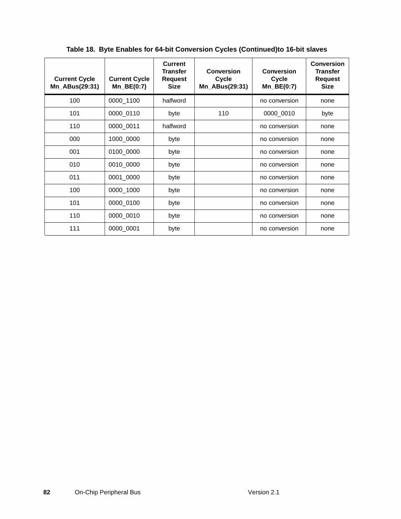
100 0000_1100 halfword no conversion none
101 0000_0110 byte 110 0000_0010 byte
110 0000_0011 halfword no conversion none
000 1000_0000 byte no conversion none
001 0100_0000 byte no conversion none
010 0010_0000 byte no conversion none
011 0001_0000 byte no conversion none
100 0000_1000 byte no conversion none
101 0000_0100 byte no conversion none
110 0000_0010 byte no conversion none
111 0000_0001 byte no conversion none
Table 18. Byte Enables for 64-bit Conversion Cycles (Continued)to 16-bit slaves
Current CycleMn_ABus(29:31)
Current CycleMn_BE(0:7)
Current TransferRequest
Size
Conversion Cycle
Mn_ABus(29:31)
Conversion Cycle
Mn_BE(0:7)
Conversion Transfer Request
Size
82 On-Chip Peripheral Bus Version 2.1

5.5.1.6 32-bit Conversion Cycle to a 16-bit Slave Byte Enables
Conversion cycles occur in the case of a 32-bit master accessing a 16-bit slave with requested bytes that are odd aligned or cross a halfword boundary. Table 19 shows the byte enables driven by the master during a conversion cycle.
Table 19. Byte Enables for Conversion Cycles
Current CycleMn_ABus(30:31)
Current CycleMn_BE(0:7)
Conversion CycleMn_BE(0:7)
Transfer Size
00 1111 0011 2 bytes
000 1110 0010 2 bytes
001 0111 0011 1 bytes
010 0011 0000_1000 3 bytes
011 0001_1100 0000_1100 3 bytes
100 0000_1110 no conversion 3 bytes
101 0000_0111 no conversion 3 bytes
000 1100_0000 no conversion 2 bytes
001 0110_0000 no conversion 2 bytes
010 0011_0000 no conversion 2 bytes
011 0001_1000 0000_1000 2 bytes
100 0000_1100 no conversion 2 bytes
101 0000_0110 no conversion 2 bytes
110 0000_0011 no conversion 2 bytes
000 1000_0000 no conversion 1 byte
001 0100_0000 no conversion 1 byte
010 0010_0000 no conversion 1 byte
011 0001_0000 no conversion 1 byte
100 0000_1000 no conversion 1 byte
101 0000_0100 no conversion 1 byte
110 0000_0010 no conversion 1 byte
111 0000_0001 no conversion 1 byte
Version 2.1 OPB Operations 83

5.5.1.7 Doubleword Master byte enable (BE) write request to a Doubleword Slave with no byte enable support
Figure 41 shows a byte enable request for a write of 6 bytes by a double word master. The slave does not implement the optional byte enable protocol. Because of address alignment the master must request a byte transfer using the Xfer size signals. The slave does not support byte enable protocol, indicated by the negation of OPB_beAck, therefore dynamic bus sizing occurs.
OPB_Clk
OPB_select
M1_select
OPB_M1Grant
M1_request
M1_RNW
Figure 40. Byte Enable request to non-Byte Enable slave
0 1 2 3 4 5 6 7 8Cycles
M1_ABus(29:31)
Sl1_xferAck
OPB_xferAck
OPB_ABus(29:31)
OPB_DBus(0:31)
M1_hwXfer
M1_DBusEn
Sl1_dwAck
transfer attempted by master
bus width ack’ed by slave
6 Byte 5 Byte 3 Byte Byte
DW DW DW DW
001 010 100 110
0:23
001 010 100 010
M1_BE 01111110 00111110 00001110 00000010
M1_dwXfer
M1_fwXfer
Sl1_hwAck
M1_beXfer
OPB_beAck
M1_DBus(0:31) B(1-3) B(2,3) B(4-6) Byte 6
M1_DBusEn32_63
M1_DBus(32:63) B(4-6) Byte 6B(4-6) B(4-6)
8:31 16:31
OPB_DBus(32:63) 32:5632:56 32:56
16:23
48:56
Sl1_fwAck
84 On-Chip Peripheral Bus Version 2.1

5.5.1.8 Doubleword Master byte enable (BE) write request to a Doubleword Slave with byte enable support
Figure 41 shows a byte enable request for a write of 6 bytes by a double word master. The slave does not implement the optional byte enable protocol. Because of address alignment the master must request a byte transfer using the Xfer size signals. The slave does not support byte enable protocol so dynamic bus sizing occurs.
OPB_Clk
OPB_select
OPB_M1Grant
M1_request
M1_RNW
Figure 41. Byte Enable request to a Byte Enable Capable 64-bit Slave
0 1 2 3 4 5 6 7 8Cycles
M1_ABus(29:31)
Sl1_xferAck
OPB_ABus(29:31)
M1_DBusEn
001
001
M1_dwXfer
M1_beXfer
OPB_beAck
OPB_xferAck
OPB_DBus(0:31) 8:31
OPB_DBus(32:63) 32:56
M1_select
M1_BE(0:7) 01111110
M1_fwXfer
M1_hwXfer
M1_DBus(0:31) B1-3
M1_DBus(32:63) B4-6
M1_DBusEn32_63
Sl1_beAck
Sl1_dwAck
Sl1_fwAck
Sl1_hwAck
Version 2.1 OPB Operations 85
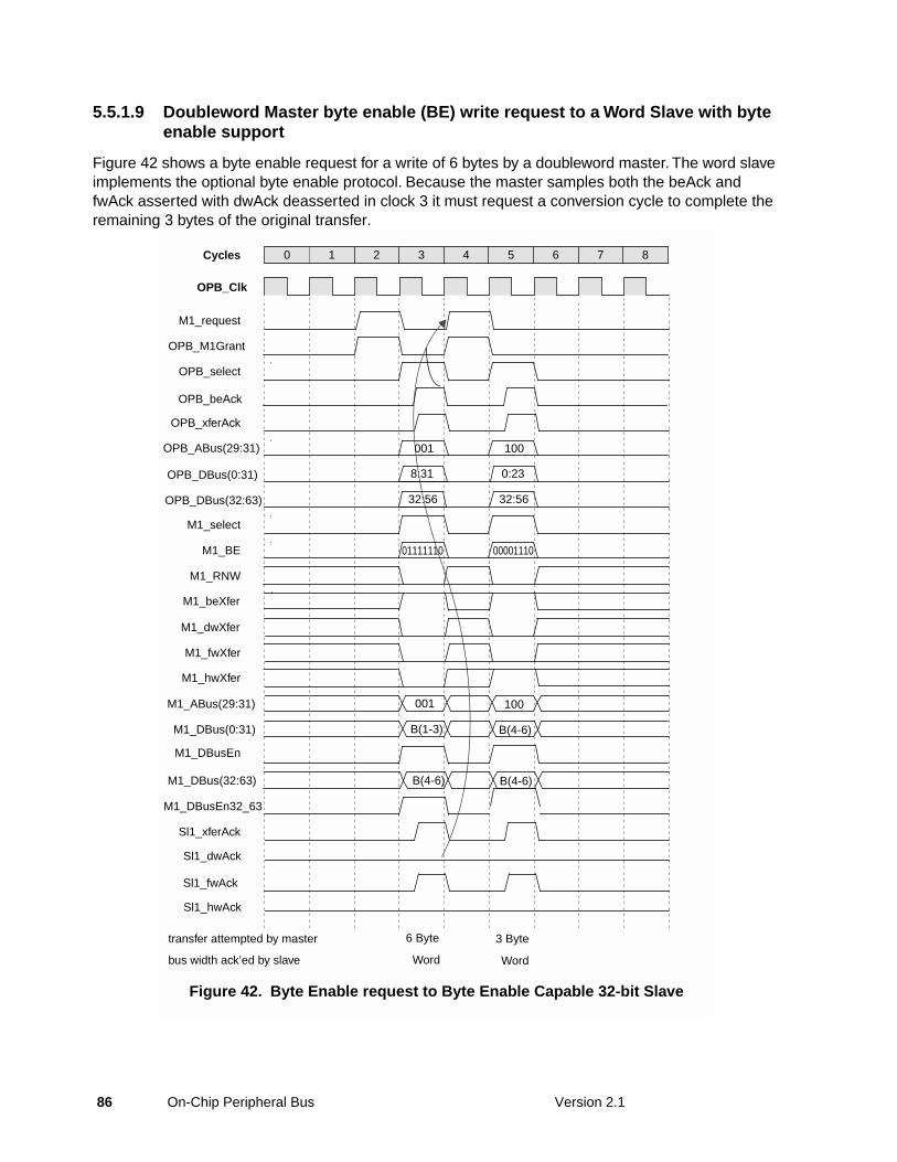
5.5.1.9 Doubleword Master byte enable (BE) write request to a Word Slave with byte enable support
Figure 42 shows a byte enable request for a write of 6 bytes by a doubleword master. The word slave implements the optional byte enable protocol. Because the master samples both the beAck and fwAck asserted with dwAck deasserted in clock 3 it must request a conversion cycle to complete the remaining 3 bytes of the original transfer.
OPB_Clk
OPB_select
M1_select
OPB_M1Grant
M1_request
M1_RNW
Figure 42. Byte Enable request to Byte Enable Capable 32-bit Slave
0 1 2 3 4 5 6 7 8Cycles
M1_ABus(29:31)
Sl1_xferAck
OPB_xferAck
OPB_ABus(29:31)
OPB_DBus(0:31)
M1_hwXfer
M1_DBusEn
transfer attempted by master
bus width ack’ed by slave
6 Byte 3 Byte
Word Word
001 100
0:23
001 100
M1_BE 01111110 00001110
M1_dwXfer
M1_fwXfer
Sl1_hwAck
M1_beXfer
OPB_beAck
M1_DBus(0:31) B(1-3) B(4-6)
M1_DBusEn32_63
M1_DBus(32:63) B(4-6)B(4-6)
8:31
OPB_DBus(32:63) 32:5632:56
Sl1_fwAck
Sl1_dwAck
86 On-Chip Peripheral Bus Version 2.1

5.6 Connection of 32-bit and 64-bit devices with byte enables
Interconnecting 64-bit masters and slaves to a 32-bit bus and 32-bit masters to a 64-bit bus with byte enables requires some unique wiring. The attachment of fullword, halfword, and byte slaves is the same whether attached to a 32 or 64-bit OPB. The following diagrams illustrate the connection of 64-bit OPB devices and implementations and only the signals associated with byte enables are shown. See Chapter 3.5, “Connection of 32-bit and 64-bit devices,” on page 3-24 for all other signal connections.
5.6.1 32-bit Master Attached To a 64-bit OPB bus byte enable connection
Figure 43 shows the 32-bit master interface signals to a 64-bit OPB implementation. Note the master Mn_BE(0:3) signals are fed into a 4-bit one to two demultiplexer with the select connected to Mn_ABus(29). See “OPB Signals” on page 6. for detailed functional signal descriptions.
OPB_beAck
Figure 43. 32-bit Master with 64-bit OPB byte enable connection
64-bit OPB 32-bit OPBMn_beXfer
Mn_BE(0:3)
Bus LogicMaster
Mn_BE(0:3)
Mn_ABus(29)
Mn_BE(4:7)
OAND
AND
Version 2.1 OPB Operations 87

5.6.2 64-bit Master Attached To a 32-bit OPB bus byte enable connection
Figure 44 shows the 64-bit master interface signals to a 32-bit OPB implementation. Note the master Mn_BE(0:7) signals are fed into a 4-bit two to one multiplexer with the select connected to Mn_ABus(29). See “OPB Signals” on page 6. for detailed functional signal descriptions.
OPB_beAck
Figure 44. 64-bit Master with 32-bit OPB byte enable connection
32-bit OPB 64-bit OPBMn_beXfer
Mn_BE(0:3)
Bus LogicMaster
Mn_BE(4:7)Mn_BE(0:3)
0
1
Mn_ABus(29)
88 On-Chip Peripheral Bus Version 2.1

5.7 Optional OPB DMA Transfers
DMA operation is specific to the system architecture and is beyond the scope of this document. The OPB architecture merely allows for the utilization of the OPB by DMA peripherals under direct control of a DMA master. Four types of optional DMA transfers are outlined here.
• DMA peripheral read or write.
• DMA peripheral burst read or write.
• DMA flyby read or write transfers.
• DMA flyby burst read or write transfers.
In the following examples, an OPB slave device acts as DMA peripheral slave device. A simple request and acknowledge handshake is used. DMA peripheral slave devices request service from the DMA by asserting the Sln_dmaReq signal. The DMA samples Sln_dmaReq signal asserted and requests the OPB bus. Once granted the DMA asserts the DMA_SlnAck signal to the appropriate peripheral slave device allowing it to drive the data bus or latch data off of the data bus.
During DMA flyby transfers a simultaneous memory read or write occurs during the peripheral access. The data is not read into the DMA instead it flows directly from source to destination. Only memory slaves and DMA peripheral slaves of the same size can perform DMA flyby transfers. In the case of a flyby peripheral read the data read from the peripheral is coincidently written into a memory slave at the selected address. In the case of a flyby peripheral write the data read from the memory slave at the selected address is coincidently latched by the DMA peripheral. A careful analysis of the memory slave, DMA peripheral slave, and the DMA must be made to insure that the timings of both the source and destination of the transfer are compatible.
The sampling of the Sln_dmaReq signal by the DMA is implementation dependent. DMA transfers utilizing the OPB for more than one clock must assert the OPB_busLock signal, in the absence of the DMA_select signal, to retain ownership of the bus. Given this operation it is possible that a DMA transfer may cause an arbitration penalty cycle. In general this should be avoided or only used for lower bandwidth slaves with infrequent requests. Peripheral slave devices with higher bandwidth requirements should utilize a Burst mode of operation performing multiple accesses per DMA master bus grant.
The following examples illustrate DMA operation on the OPB.
Version 2.1 OPB Operations 89

5.7.1 DMA Peripheral Read Cycle
Figure 45 shows an optional DMA peripheral read cycle. In the following example, the OPB slave device acts as DMA peripheral slave device. The DMA peripheral asserts the DMA request signal, Sl1_dmaReq. The DMA master samples request asserted and requests the OPB by asserting M0_request. The DMA master is granted the OPB via OPB_M0Grant assertion. The DMA master asserts DMA_Sl1Ack. The DMA peripheral drives the OPB_DBus with the read data. The DMA master latches the data and deasserts DMA_Sl1Ack completing the access. Since the DMA sampled the Sl1_dmaReq signal asserted at the end of clock 4 another transfer is performed. Note the OPB device only outputs data to OPB_DBus when the DMA acknowledge signal is asserted. The assertion of DMA_Sl1Ack causes the peripheral to deassert its request signal during clock 6. No further transfers are performed by the DMA.
OPB_Clk
OPB_busLock
OPB_DBus
DMA_Sl1Ack
Sl1_dmaReq
M0_request
OPB_M0Grant
Figure 45. DMA Peripheral Read Cycle
0 1 2 3 4 5 6 7Cycles
OPB_select
Sl1_DBus
Sl1_DBusEn
D0 D1
D0 D1
OPB_ABus
90 On-Chip Peripheral Bus Version 2.1

5.7.2 DMA Peripheral Write Cycle
Figure 46 shows an optional DMA peripheral write cycle. In the following example, the OPB slave device acts as DMA peripheral slave device. The DMA peripheral asserts the DMA request signal, Sl1_dmaReq. The DMA master samples Sl1_dmaReq asserted and requests the OPB by asserting M0_request. The DMA master is granted the OPB via OPB_M0Grant assertion. The DMA master asserts DMA_Sl1Ack and drives the OPB_DBus with data. The DMA peripheral latches the OPB_DBus write data. The DMA master deasserts DMA_Sl1Ack completing the access. Since the DMA sampled the Sl1_dmaReq signal asserted at the end of clock 4 another transfer is performed. The assertion of DMA_Sl1Ack causes the peripheral to deassert its request signal during clock 6. No further transfers are performed by the DMA.
OPB_Clk
OPB_busLock
OPB_DBus
DMA_Sl1Ack
Sl1_dmaReq
M0_request
OPB_M0Grant
Figure 46. DMA Peripheral Write Cycle
0 1 2 3 4 5 6 7Cycles
OPB_select
M0_DBus
M0_DBusEn
D0 D1
D0 D1
OPB_ABus
Version 2.1 OPB Operations 91

5.7.3 DMA Burst Peripheral Read Cycle
Figure 47 shows an optional DMA burst peripheral read cycle. The DMA peripheral slave asserts the DMA request signal, Sl1_dmaReq. The DMA master samples request asserted and requests the OPB by asserting M0_request. The DMA master is granted the OPB via OPB_M0Grant assertion. The DMA master asserts DMA_Sl1Ack and locks the OPB by asserting M0_busLock. The DMA peripheral drives the OPB_DBus with the read data in clock 3. The DMA latches the data. The peripheral slave drives the next data for clocks 4, 5, and 6. The DMA samples the Sl1_dmaReq signal deasserted in clock 6. The DMA master deasserts DMA_Sl1Ack and M0_busLock completing the access. Note that this operation will cause an arbitration penalty cycle. Two options to eliminate this condition are to have the DMA and slave set to a preprogrammed “fixed burst length”, letting the DMA know when to deassert busLock, or use Sln_dmaReq to combinatorially gate off the DMA busLock signal.
OPB_Clk
OPB_busLock
OPB_DBus
DMA_Sl1Ack
Sl1_dmaReq
M0_request
OPB_M0Grant
Figure 47. DMA Burst Peripheral Read Cycles
0 1 2 3 4 5 6 7Cycles
OPB_select
D0 D3
OPB_ABus
D1 D2
Sl1_DBusEn
M0_busLock
Sl1_DBus D0 D3D1 D2
92 On-Chip Peripheral Bus Version 2.1

5.7.4 DMA Burst Peripheral Write Cycle
Figure 48 shows an optional DMA burst peripheral write cycle. The DMA peripheral slave asserts the DMA request signal, Sl1_dmaReq. The DMA master samples request asserted and requests the OPB by asserting M0_request. The DMA master is granted the OPB via OPB_M0Grant assertion. The DMA master asserts DMA_Sl1Ack and locks the OPB by asserting M0_busLock. The DMA drives the OPB_DBus with the write data in clock 3. The DMA peripheral slave latches the data. The DMA drives the next data for clocks 4, 5, and 6. The DMA samples the Sl1_dmaReq signal deasserted in clock 6. The DMA master deasserts DMA_Sl1Ack and M0_busLock completing the access. Note that this operation will cause an arbitration penalty cycle. Two options to eliminate this condition are to have the DMA and slave set to a preprogrammed “fixed burst length”, letting the DMA know when to deassert busLock, or use Sln_dmaReq to combinatorially gate off the DMA busLock signal.
OPB_Clk
OPB_busLock
OPB_DBus
DMA_Sl1Ack
Sl1_dmaReq
M0_request
OPB_M0Grant
Figure 48. DMA Burst Peripheral Write Cycles
0 1 2 3 4 5 6 7Cycles
OPB_select
D0 D3
OPB_ABus
D1 D2
M0_DBusEn
M0_DBus D0 D3D1 D2
M0_busLock
Version 2.1 OPB Operations 93

5.7.5 DMA Flyby Memory Read Peripheral Write Cycle
In the example of Figure 49 one OPB slave device acts as a memory slave and the other as a DMA peripheral slave device. The DMA peripheral asserts the DMA request signal, Sl1_dmaReq. The DMA master samples request asserted and requests the OPB by asserting M0_request. The DMA master is granted the OPB via OPB_M0Grant assertion. The DMA master asserts M0_select with the source memory address. The memory slave has a read latency of one clock. The DMA is programmed with DMA_Sl1Ack assertion delay of one, setup=1. In clock 5 the memory slave drives read data and the DMA asserts DMA_Sl1Ack. The DMA peripheral deasserts Sl1_dmaReq and latches the read data from the OPB_DBus. The DMA master deasserts DMA_Sl1Ack completing the access
OPB_Clk
OPB_DBus
DMA_Sl1Ack
Sl1_dmaReq
M0_request
OPB_DMAGrant
Figure 49. DMA Flyby Memory Read Peripheral Write Cycle
0 1 2 3 4 5 6 7Cycles
OPB_select
D0
OPB_busLock
OPB_ABus
Sl1_DBus D0
Sl1_DBusEn
A0
Sl1_xferAck
Setup =1
M0_select
M0_RNW
M0_ABus A0
94 On-Chip Peripheral Bus Version 2.1

5.7.6 DMA Flyby Peripheral Read Memory Write Cycle
In the example of Figure 50 OPB slave device 2 acts as a memory slave and device 1 as a DMA peripheral slave device. The DMA peripheral asserts the DMA request signal, Sl1_dmaReq. The DMA master samples request asserted and requests the OPB by asserting M0_request. The DMA master is granted the OPB via OPB_M0Grant assertion. The DMA master asserts M0_select with the destination memory address and the DMA_Sl1Ack signal. The DMA peripheral slave drives read data and deasserts Sl1_dmaReq. The memory slave asserts Sl1_xferAck and latches the read data from OPB_DBus. The DMA master deasserts DMA_Sl1Ack completing the access
OPB_Clk
OPB_DBus
DMA_Sl1Ack
Sl1_dmaReq
M0_request
OPB_DMAGrant
Figure 50. DMA Flyby Peripheral Read Memory Write Cycle
0 1 2 3 4 5 6 7Cycles
OPB_select
D0
OPB_busLock
OPB_ABus
Sl1_DBus D0
Sl1_DBusEn
A0
Sl2_xferAck
M0_select
M0_RNW
M0_ABus A0
Version 2.1 OPB Operations 95

5.7.7 DMA Flyby Burst Cycle Memory Read Peripheral Write
In the example of Figure 51 one OPB slave device acts as a memory slave and the other as a DMA peripheral slave device. The DMA peripheral asserts the DMA request signal, Sl1_dmaReq. The DMA master samples request asserted and requests the OPB by asserting M0_request. The DMA master is granted the OPB via OPB_M0Grant assertion. The DMA master asserts M0_busLock, DMA_Sl1Ack, and M0_select with the source memory address. The memory slave drives read data and the DMA peripheral latches the read data from OPB_DBus. This sequence continues until clock 6 when the peripheral deasserts Sl1_dmaReq. One final transfer occurs. The DMA master deasserts DMA_Sl1Ack and M0_busLock completing the access
OPB_Clk
OPB_DBus
DMA_Sl1Ack
Sl1_dmaReq
M0_request
OPB_M0Grant
Figure 51. DMA Flyby Burst Memory Read Peripheral Write Cycle
0 1 2 3 4 5 6 7Cycles
D0
OPB_ABus
D1 D2
Sl1_DBus D0 D1 D2
Sl1_DBusEn
OPB_RNW
Sl1_xferAck
M0_select
OPB_select
M0_RNW
OPB_busLock
A0 A1 A2 A3
D3
D3
96 On-Chip Peripheral Bus Version 2.1

5.7.8 DMA Flyby Burst Cycle Peripheral Read Memory Write
In the example of Figure 52 OPB slave device 2 acts as a memory slave and slave device 1 as a DMA peripheral slave device. The DMA peripheral asserts the DMA request signal, Sl1_dmaReq. The DMA master samples request asserted and requests the OPB by asserting M0_request. The DMA master is granted the OPB via OPB_M0Grant assertion. The DMA master asserts M0_busLock, DMA_Sl1Ack, and M0_select with the destination memory address. The peripheral slave drives read data and the memory slave latches the read data from OPB_DBus. This sequence continues until clock 6 when the peripheral deasserts Sl1_dmaReq. One final transfer occurs. The DMA master deasserts DMA_Sl1Ack and M0_busLock completing the access
OPB_Clk
DMA_Sl1Ack
Sl1_dmaReq
M0_request
OPB_M0Grant
Figure 52. DMA Flyby Burst Peripheral Read Memory Write Cycle
0 1 2 3 4 5 6 7Cycles
OPB_ABus
Sl1_DBusEn
OPB_RNW
Sl2_xferAck
M0_select
OPB_select
M0_RNW
OPB_busLock
A0 A1 A2 A3
Sl1_DBus A0 A1 A2 A3
OPB_DBus A0 A1 A2 A3
Version 2.1 OPB Operations 97

98 On-Chip Peripheral Bus Version 2.1

Index
Numerics32-bit conversion cycle to a 16-bit slave with
byte enables 8332-bit master attached to 64-bit OPB bus byte
enable connection 8732-bit master attached to a 64-bit OPB bus 2732-bit master write data mirroring 5532-bit master write data mirroring with byte
enables 7532-bit slave attached to a 64-bit OPB bus 2864-bit conversion cycle to a 16-bit slave with
byte enables 8164-bit conversion cycle to a 32-bit slave with
byte enables 7964-bit master attached to 32-bit OPB bus byte
enable connection 8864-bit master attached to a 32-bit OPB bus 2564-bit master write data mirroring 5664-bit master write data mirroring with byte
enables 7664-bit slave attached to a 32-bit OPB bus 2664-bit slave read data steering 5764-bit slave read data steering for 32-bit master
byte enables 78
Aabout this book 13arbiter output connection
on-chip peripheral bus 5
Bbye enable signaling and operation 74
Cconnection of 32-bit and 64-bit devices 24connection to a 32-bit and 64-bit devices with
byte enables 87conversion cycles 58
doubleword conversion 59fullword cycles 58halfword cycles 58
Ddata transfer with dynamic bus sizing 59DMA_SlnAck 17doubleword master byte enable write request to
a doubleword slave with byteenable 85
doubleword master byte enable write request to
a doubleword slave with no byteenable 84
doubleword master byte enable write request toa word slave with byte enable 86
Mmaster output connection
on-chip peripheral bus 4Mn_ABus(0:31) 11Mn_BE(0
/7) 16Mn_beXfer 16Mn_busLock 9Mn_DBus(0:64) 11Mn_DBusEn 13, 14Mn_fwXfer 13Mn_hwXfer 13Mn_request 8Mn_RNW 12Mn_select 12Mn_seqAddr 13Mn_UABus(0:31) 11
Oon-chip peripheral bus 1
arbiter output connection 5arbitration signals 8bus signals 11byte enable support signals 16data transfer control signals 12DMA support signals 17features 1implementation 3interfaces 20
arbiter 23DMA 24master 21slave 22
master output connection 4operations 32signal naming conventions 6signals 6slave output connection 5timing guidelines 29
OPB 1OPB byte enable architecture 74OPB data transfers 38
basic data 38
Version 2.1 Index 99

bus lock 44bus lock penalty case 45continuous bus request 43one cycle latency 39overlapped bus arbitration 41sequential address signal 46two cycle latency 40
OPB DMA transfers 89DMA burst peripheral read 92DMA burst peripheral write 93DMA flyby burst cycle memory read peripher-
al write 96DMA flyby burst cycle peripheral read memo-
ry write 97DMA flyby memory read peripheral write 94DMA flyby peripheral read memory write 95DMA peripheral read 90DMA peripheral write 91
OPB latency register implementation 73OPB master latency 72
latency counter 72latency counter expiration 72latency counter implementation 72
OPB transfersbus arbitration 32
basic 32bus lock signal 34bus master priority 36bus parking 37continuous bus request 33multiple bus request 35
bus timeout error 50dynamic bus sizing 53
byte write operation 64data alignment 53fullword byte read 61fullword byte read and write 70fullword halfword read and write 59fullword read and write 62halfword byte read 63halfword byte read and write 71locked with interruption 66locked with no interruption 68master transfer slave sizing 54overlapped arbitration 65read data mirroring 54write data mirroring 54
OPB master abort 49slave retry
bus timeout error condition 51bus timeout error suppression 52
slave retry operation 47
OPB_ABus(0:31) 11OPB_BE(0
/7) 16OPB_beAck 16OPB_beXfer 16OPB_busLock 9OPB_DBus(0:64) 11OPB_errAck 15OPB_fwAck 14OPB_fwXfer 13OPB_hwAck 14OPB_hwXfer 13OPB_MnGrant 9OPB_pendReqn 9OPB_retry 10OPB_RNW 12OPB_select 12OPB_seqAddr 13OPB_timeout 10OPB_toutSup 15OPB_UABus(0:31) 11OPB_xferAck 14optional signal enumeration 18
Ssignals
arbitration 8byte enable support 16data transfer control 12DMA support 17DMA_SlnAck 17Mn_ABus(0:31) 11Mn_BE(0
/7) 16Mn_beXfer 16Mn_busLock 9Mn_DBus(0:64) 11Mn_DBusEn 13, 14Mn_fwXfer 13Mn_hwXfer 13Mn_request 8Mn_RNW 12Mn_select 12Mn_seqAddr 13Mn_UABus(0:31) 11naming conventions 6on-chip peripheral bus 6OPB_ABus(0:31) 11OPB_BE(0
/7) 16OPB_beAck 16OPB_beXfer 16
100 On-Chip Peripheral Bus Version 2.1

OPB_busLock 9OPB_DBus(0:64) 11OPB_errAck 15OPB_fwAck 14OPB_fwXfer 13OPB_hwAck 14OPB_hwXfer 13OPB_MnGrant 9OPB_pendReqn 9OPB_retry 10OPB_RNW 12OPB_select 12OPB_seqAddr 13OPB_timeout 10OPB_toutSup 15OPB_UABus(0:31) 11OPB_xferAck 14Sl_hwAck 14SLn_beAck 16Sln_DBus(0:64) 11Sln_DBusEn 13, 14Sln_dmaReq 17Sln_errAck 15Sln_fwAck 14Sln_retry 10Sln_toutSup 15Sln_xferAck 14
slave output connectionon-chip peripheral bus 5
SLn_beAck 16Sln_DBus(0:64) 11Sln_DBusEn 13, 14Sln_dmaReq 17Sln_errAck 15Sln_fwAck 14Sln_hwAck 14Sln_retry 10Sln_toutSup 15Sln_xferAck 14
Ttiming guidelines
on-chip peripheral bus 29
Version 2.1 Index 101

102 On-Chip Peripheral Bus Version 2.1


© International Business Machines Corporation 1996 - 2001Printed in the United States of America4/17/01All Rights Reserved
The information contained in this document is subject to change without notice. The products described in this document are NOT intended for use in implantation or other life support applications where malfunction may result in injury or death to persons. The information contained in this document does not affect or change IBM’s product specifications or warranties. Nothing in this document shall operate as an express or implied license or indemnity under the intellectual property rights of IBM or third parties. All information contained in this document was obtained in specific environments, and is presented as illustration. The results obtained in other operating environments may vary.
While the information contained herein is believed to be accurate, such information is preliminary, and should not be relied upon for accuracy or completeness, and no representations or warranties of accuracy or completeness are made.
THE INFORMATION CONTAINED IN THIS DOCUMENT IS PROVIDED ON AN “AS IS” BASIS. In no event will IBM be liable for any damages arising directly or indirectly from any use of the information contained in this document.
IBM Microelectronics Division 1580 Route 52, Bldg. 504 Hopewell Junction, NY 12533-6531
The IBM home page can be found at http://www.ibm.com
The IBM Microelectronics Division home page can be found at http://www.chips.ibm.com
Document No. SA-14-2528-02