on detection, analysis and characterization of transient
TRANSCRIPT

University of Massachusetts Amherst University of Massachusetts Amherst
ScholarWorks@UMass Amherst ScholarWorks@UMass Amherst
Open Access Dissertations
5-2010
On Detection, Analysis and Characterization of Transient and On Detection, Analysis and Characterization of Transient and
Parametric Failures in Nano-scale CMOS VLSI Parametric Failures in Nano-scale CMOS VLSI
Alodeep Sanyal University of Massachusetts Amherst
Follow this and additional works at: https://scholarworks.umass.edu/open_access_dissertations
Part of the Electrical and Computer Engineering Commons
Recommended Citation Recommended Citation Sanyal, Alodeep, "On Detection, Analysis and Characterization of Transient and Parametric Failures in Nano-scale CMOS VLSI" (2010). Open Access Dissertations. 243. https://scholarworks.umass.edu/open_access_dissertations/243
This Open Access Dissertation is brought to you for free and open access by ScholarWorks@UMass Amherst. It has been accepted for inclusion in Open Access Dissertations by an authorized administrator of ScholarWorks@UMass Amherst. For more information, please contact [email protected].
ON DETECTION, ANALYSIS AND
CHARACTERIZATION OF TRANSIENT ANDPARAMETRIC FAILURES IN NANO-SCALE CMOS VLSI
A Dissertation Presented
by
ALODEEP SANYAL
Submitted to the Graduate School of theUniversity of Massachusetts Amherst in partial fulfillment
of the requirements for the degree of
DOCTOR OF PHILOSOPHY
May 2010
Electrical and Computer Engineering

c© Copyright by Alodeep Sanyal 2010
All Rights Reserved
ON DETECTION, ANALYSIS ANDCHARACTERIZATION OF TRANSIENT AND
PARAMETRIC FAILURES IN NANO-SCALE CMOS VLSI
A Dissertation Presented
by
ALODEEP SANYAL
Approved as to style and content by:
Sandip Kundu, Chair
Maciej Ciesielski, Member
Israel Koren, Member
Robert Moll, Member
Christopher V. Hollot, Department ChairElectrical and Computer Engineering

To my parents Alok Subhra and Dipa
andMy wife Debalina

ACKNOWLEDGMENTS
I would like to take this opportunity to pay my sincerest thanks and gratitude to
my advisor Prof. Sandip Kundu for his mentoring, guidance and relentless support
during the entire course of this Doctoral thesis work. I would also like to thank my
thesis committee members Prof. Maciej Ciesielski, Prof. Israel Koren, and Prof.
Robert Moll for their insightful comments and valuable suggestions.
I feel truly grateful to my friends and colleagues in the Electrical and Computer
Engineering Department for their unforgettable support and commitment during
my thesis research. My colleagues at Advanced VLSI Design and Test Laboratory,
namely, Kunal Ganeshpure, Aswin Sreedhar, Ashesh Rastogi, Wei Chen, Kelagari Na-
garaj, Aarti Chhowdhary, Spandana Remarsu, Abhisek Pan, Michael Buttrick and
others extended all sorts of help and support whenever needed. I will never be able to
forget the consistent encouragement and support I got from my friend Basab Datta
during these years. Without everyone’s kind support and enthusiasm, this research
could not have been completed in its present perspective.
Finally, I am deeply indebted to my family, whose unfathomable love, moral sup-
port and encouragement only made this effort possible. And my wife Debalina, with
whom I walk everyday by the side of a river, through a dense forest, into a locality,
in quest of an indomitable ray of sunshine.
v
ABSTRACT
ON DETECTION, ANALYSIS AND
CHARACTERIZATION OF TRANSIENT ANDPARAMETRIC FAILURES IN NANO-SCALE CMOS VLSI
MAY 2010
ALODEEP SANYAL
B.TECH., UNIVERSITY OF KALYANI, INDIA
MS, COLORADO STATE UNIVERSITY, USA
Ph.D., UNIVERSITY OF MASSACHUSETTS AMHERST
Directed by: Professor Sandip Kundu
As we move deep into nanometer regime of CMOS VLSI (45nm node and be-
low), the device noise margin gets sharply eroded because of continuous lowering
of device threshold voltage together with ever increasing rate of signal transitions
driven by the consistent demand for higher performance. Sharp erosion of device
noise margin vastly increases the likelihood of intermittent failures (also known as
parametric failures) during device operation as opposed to permanent failures caused
by physical defects introduced during manufacturing process. The major sources of
intermittent failures are capacitive crosstalk between neighbor interconnects, abnor-
mal drop in power supply voltage (also known as droop), localized thermal gradient,
and soft errors caused by impact of high energy particles on semiconductor surface.
In nanometer technology, these intermittent failures largely outnumber the perma-
nent failures caused by physical defects. Therefore, it is of paramount importance
vi
to come up with efficient test generation and test application methods to accurately
detect and characterize these classes of failures.
Soft error rate (SER) is an important design metric used in semiconductor in-
dustry and represented by number of such errors encountered per Billion hours of
device operation, known as Failure-In-Time (FIT) rate. Soft errors are rare events.
Traditional techniques for SER characterization involve testing multiple devices in
parallel, or testing the device while keeping it in a high energy neutron bombardment
chamber to artificially accelerate the occurrence of single events. Motivated by the
fact that measurement of SER incurs high time and cost overhead, in this thesis, we
propose a two step approach: 〈i〉 a new filtering technique based on amplitude of the
noise pulse, which significantly reduces the set of soft error susceptible nodes to be
considered for a given design; followed by 〈ii〉 an Integer Linear Program (ILP)-based
pattern generation technique that accelerates the SER characterization process by
1-2 orders of magnitude compared to the current state-of-the-art.
During test application, it is important to distinguish between an intermittent
failure and a permanent failure. Motivated by the fact that most of the intermit-
tent failures are temporally sparse in nature, we present a novel design-for-testability
(DFT) architecture which facilitates application of the same test vector twice in a
row. The underlying assumption here is that a soft fail will not manifest its effect in
two consecutive test cycles whereas the error caused by a physical defect will produce
an identically corrupt output signature in both test cycles. Therefore, comparing
the output signature for two consecutive applications of the same test vector will
accurately distinguish between a soft fail and a hard fail. We show application of
this DFT technique in measuring soft error rate as well as other circuit marginality
related parametric failures, such as thermal hot-spot induced delay failures.
A major contribution of this thesis lies on investigating the effect of multiple
sources of noise acting together in exacerbating the noise effect even further. The
vii
existing literature on signal integrity verification and test falls short of taking the
combined noise effects into account. We particularly focus on capacitive crosstalk on
long signal nets. A typical long net is capacitively coupled with multiple aggressors
and also tend to have multiple fanout gates. Gate leakage current that originates
in fanout receivers, flows backward and terminates in the driver causing a shift in
driver output voltage. This effect becomes more prominent as gate oxide is scaled
more aggressively. In this thesis, we first present a dynamic simulation-based study
to establish the significance of the problem, followed by proposing an automatic test
pattern generation (ATPG) solution which uses 0-1 Integer Linear Program (ILP)
to maximize the cumulative voltage noise at a given victim net due to crosstalk and
gate leakage loading in conjunction with propagating the fault effect to an observation
point. Pattern pairs generated by this technique are useful for both manufacturing
test application as well as signal integrity verification for nanometer designs. This
research opens up a new direction for studying nanometer noise effects and motivates
us to extend the study to other noise sources in tandem including voltage drop and
temperature effects.
viii

TABLE OF CONTENTS
Page
ACKNOWLEDGMENTS . . . . . . . . . . . . . . . . . . . . . . . . . . . . . . . . . . . . . . . . . . . . . v
ABSTRACT . . . . . . . . . . . . . . . . . . . . . . . . . . . . . . . . . . . . . . . . . . . . . . . . . . . . . . . . . . vi
LIST OF TABLES . . . . . . . . . . . . . . . . . . . . . . . . . . . . . . . . . . . . . . . . . . . . . . . . . . .xiii
LIST OF FIGURES . . . . . . . . . . . . . . . . . . . . . . . . . . . . . . . . . . . . . . . . . . . . . . . . . .xiv
CHAPTER
1. INTRODUCTION . . . . . . . . . . . . . . . . . . . . . . . . . . . . . . . . . . . . . . . . . . . . . . . . . 1
2. SOFT ERRORS AND IMPROVED MEASUREMENTTECHNIQUES FOR SOFT ERROR RATE . . . . . . . . . . . . . . . . . . . . . 7
2.1 Introduction . . . . . . . . . . . . . . . . . . . . . . . . . . . . . . . . . . . . . . . . . . . . . . . . . . . . . 72.2 Background and Related Work . . . . . . . . . . . . . . . . . . . . . . . . . . . . . . . . . . . . . 9
2.2.1 The Soft Error Problem . . . . . . . . . . . . . . . . . . . . . . . . . . . . . . . . . . . . . 92.2.2 Failure-In-Time (FIT) Rate . . . . . . . . . . . . . . . . . . . . . . . . . . . . . . . . . 112.2.3 Factors Affecting the FIT Rate . . . . . . . . . . . . . . . . . . . . . . . . . . . . . . 112.2.4 Measurement of FIT Rate . . . . . . . . . . . . . . . . . . . . . . . . . . . . . . . . . . 122.2.5 Related Work . . . . . . . . . . . . . . . . . . . . . . . . . . . . . . . . . . . . . . . . . . . . . 14
2.3 Node Vulnerability . . . . . . . . . . . . . . . . . . . . . . . . . . . . . . . . . . . . . . . . . . . . . . . 162.4 Strength Filtering-based Preprocessing . . . . . . . . . . . . . . . . . . . . . . . . . . . . . 17
2.4.1 Problem Definition . . . . . . . . . . . . . . . . . . . . . . . . . . . . . . . . . . . . . . . . 172.4.2 Derivation of Closed Form Expression for Vout . . . . . . . . . . . . . . . . . 192.4.3 Closed Form Expression for Logic Switching Threshold
Voltage . . . . . . . . . . . . . . . . . . . . . . . . . . . . . . . . . . . . . . . . . . . . . . . 25
2.4.3.1 Logic Switching Threshold for Inverter . . . . . . . . . . . . . . . 262.4.3.2 Logic threshold for 2-input NAND gate . . . . . . . . . . . . . . 27
ix
2.5 The Test Pattern Generation Problem . . . . . . . . . . . . . . . . . . . . . . . . . . . . . . 292.6 Automatic Test Pattern Generation-based Technique . . . . . . . . . . . . . . . . . 342.7 Integer Linear Programming (ILP)-based Technique . . . . . . . . . . . . . . . . . . 35
2.7.1 ILP Formulation . . . . . . . . . . . . . . . . . . . . . . . . . . . . . . . . . . . . . . . . . . 372.7.2 Don’t Care Generation (Xgen) . . . . . . . . . . . . . . . . . . . . . . . . . . . . . . 382.7.3 Fault Effect Propagation . . . . . . . . . . . . . . . . . . . . . . . . . . . . . . . . . . . 39
2.8 Design-For-Testability to Facilitate SER Measurement . . . . . . . . . . . . . . . . 392.9 Experimental Results . . . . . . . . . . . . . . . . . . . . . . . . . . . . . . . . . . . . . . . . . . . . 42
2.9.1 Simulation Results for Strength Filtering . . . . . . . . . . . . . . . . . . . . . 422.9.2 Simulation Results for SETPG Technique . . . . . . . . . . . . . . . . . . . . 442.9.3 Simulation Results for ILP-based Technique . . . . . . . . . . . . . . . . . . 46
2.10 Conclusions and Future Directions . . . . . . . . . . . . . . . . . . . . . . . . . . . . . . . . . 47
3. BUILT-IN SELF-TEST FOR DETECTION ANDCHARACTERIZATION OF TRANSIENT ANDPARAMETRIC FAILURES . . . . . . . . . . . . . . . . . . . . . . . . . . . . . . . . . . . . 49
3.1 Introduction . . . . . . . . . . . . . . . . . . . . . . . . . . . . . . . . . . . . . . . . . . . . . . . . . . . . 493.2 Application I – Soft Error Rate Characterization . . . . . . . . . . . . . . . . . . . . . 52
3.2.1 Background and Related Work . . . . . . . . . . . . . . . . . . . . . . . . . . . . . . 523.2.2 The Proposed Architecture . . . . . . . . . . . . . . . . . . . . . . . . . . . . . . . . . 55
3.2.2.1 Pattern Generation . . . . . . . . . . . . . . . . . . . . . . . . . . . . . . . . 563.2.2.2 Response Analysis . . . . . . . . . . . . . . . . . . . . . . . . . . . . . . . . . 58
3.2.3 Built-In Self-Test Operation . . . . . . . . . . . . . . . . . . . . . . . . . . . . . . . . 603.2.4 Applicability of the Scheme . . . . . . . . . . . . . . . . . . . . . . . . . . . . . . . . . 613.2.5 DFT Extension to Facilitate Application of Targeted
Patterns . . . . . . . . . . . . . . . . . . . . . . . . . . . . . . . . . . . . . . . . . . . . . . 633.2.6 Architecture for Testerless Test Scheduling and Test
Methodology . . . . . . . . . . . . . . . . . . . . . . . . . . . . . . . . . . . . . . . . . . 67
3.3 Application II – Test for Circuit Marginality Faults . . . . . . . . . . . . . . . . . . 68
3.3.1 Background and Related Work . . . . . . . . . . . . . . . . . . . . . . . . . . . . . . 683.3.2 The Proposed Architecture . . . . . . . . . . . . . . . . . . . . . . . . . . . . . . . . . 69
3.3.2.1 Pattern Generation . . . . . . . . . . . . . . . . . . . . . . . . . . . . . . . . 703.3.2.2 Response Analysis . . . . . . . . . . . . . . . . . . . . . . . . . . . . . . . . . 71
3.3.3 Built-In Self-Test Operation . . . . . . . . . . . . . . . . . . . . . . . . . . . . . . . . 723.3.4 Operation Mechanism. . . . . . . . . . . . . . . . . . . . . . . . . . . . . . . . . . . . . . 74
x
3.3.5 Characterization of Impact on Neighborhood . . . . . . . . . . . . . . . . . . 75
3.4 Overhead of the Scheme . . . . . . . . . . . . . . . . . . . . . . . . . . . . . . . . . . . . . . . . . . 763.5 Cost-benefit Analysis of the Proposed Approach . . . . . . . . . . . . . . . . . . . . . 783.6 Conclusions . . . . . . . . . . . . . . . . . . . . . . . . . . . . . . . . . . . . . . . . . . . . . . . . . . . . . 78
4. STUDY OF MULTIPLE AGGRESSOR CROSSTALK NOISEIN PRESENCE OF SELF-LOADING EFFECTS . . . . . . . . . . . . . . . 80
4.1 Introduction . . . . . . . . . . . . . . . . . . . . . . . . . . . . . . . . . . . . . . . . . . . . . . . . . . . . 804.2 Related Work . . . . . . . . . . . . . . . . . . . . . . . . . . . . . . . . . . . . . . . . . . . . . . . . . . . 82
4.2.1 Crosstalk Noise Models . . . . . . . . . . . . . . . . . . . . . . . . . . . . . . . . . . . . 834.2.2 Resistance-Capacitance (RC) Extraction from Layout . . . . . . . . . . 834.2.3 ATPG for Crosstalk . . . . . . . . . . . . . . . . . . . . . . . . . . . . . . . . . . . . . . . 83
4.3 Signal Delay Model . . . . . . . . . . . . . . . . . . . . . . . . . . . . . . . . . . . . . . . . . . . . . . 844.4 Impact of Loading Effect on Signal Integrity Analysis . . . . . . . . . . . . . . . . . 86
4.4.1 Model for Loading Effect-induced Noise CurrentEstimation . . . . . . . . . . . . . . . . . . . . . . . . . . . . . . . . . . . . . . . . . . . . 87
4.4.2 Model for Capacitive Crosstalk-induced Noise CurrentEstimation . . . . . . . . . . . . . . . . . . . . . . . . . . . . . . . . . . . . . . . . . . . . 93
4.4.3 Combined Noise Effect during Signal Integrity Analysis . . . . . . . . . 95
4.5 Static Analysis of Crosstalk-induced Logic Violations . . . . . . . . . . . . . . . . . 964.6 Dynamic Simulation to Evaluate Combined Noise Effect . . . . . . . . . . . . . . 97
4.6.1 Proposed Dynamic Simulation Technique . . . . . . . . . . . . . . . . . . . . . 974.6.2 Limitations of the Proposed Approach . . . . . . . . . . . . . . . . . . . . . . 100
4.7 Pattern Generation to Maximize Combined Noise Effect . . . . . . . . . . . . . 100
4.7.1 Circuit Transformation . . . . . . . . . . . . . . . . . . . . . . . . . . . . . . . . . . . . 101
4.7.1.1 Time Domain Expansion to Incorporate GateDelays . . . . . . . . . . . . . . . . . . . . . . . . . . . . . . . . . . . . . . . 101
4.7.1.2 Fault Effect Propagation . . . . . . . . . . . . . . . . . . . . . . . . . . 104
4.7.2 ILP Formulation . . . . . . . . . . . . . . . . . . . . . . . . . . . . . . . . . . . . . . . . . 104
4.7.2.1 Constraints for Maximal Crosstalk Noise . . . . . . . . . . . . 1064.7.2.2 Constraint for Maximal Gate Leakage Loading
Noise . . . . . . . . . . . . . . . . . . . . . . . . . . . . . . . . . . . . . . . . 1074.7.2.3 Objective Function for the Combined Signal
Noise . . . . . . . . . . . . . . . . . . . . . . . . . . . . . . . . . . . . . . . . 1104.7.2.4 Constraints for Fault Effect Propagation . . . . . . . . . . . . 110
xi
4.7.3 ILP-based Test Pattern Generation Algorithm . . . . . . . . . . . . . . . 1124.7.4 Scalability of the Proposed ATPG Solution . . . . . . . . . . . . . . . . . . 114
4.7.4.1 Performance . . . . . . . . . . . . . . . . . . . . . . . . . . . . . . . . . . . . . 1144.7.4.2 Test Compression . . . . . . . . . . . . . . . . . . . . . . . . . . . . . . . . 1154.7.4.3 Beyond Unit Delay . . . . . . . . . . . . . . . . . . . . . . . . . . . . . . . 117
4.8 Experimental Results . . . . . . . . . . . . . . . . . . . . . . . . . . . . . . . . . . . . . . . . . . . 117
4.8.1 Experimental Setup . . . . . . . . . . . . . . . . . . . . . . . . . . . . . . . . . . . . . . 1174.8.2 Results for Dynamic Simulation-based Study . . . . . . . . . . . . . . . . . 118
4.8.2.1 Parasitic RC Extraction . . . . . . . . . . . . . . . . . . . . . . . . . . . 1184.8.2.2 Extraction of Slew Data . . . . . . . . . . . . . . . . . . . . . . . . . . 1184.8.2.3 Pattern-dependent Dynamic Simulation . . . . . . . . . . . . . 119
4.8.3 ATPG Results . . . . . . . . . . . . . . . . . . . . . . . . . . . . . . . . . . . . . . . . . . . 120
4.9 Conclusions and Future Directions . . . . . . . . . . . . . . . . . . . . . . . . . . . . . . . . 122
5. CONCLUSIONS . . . . . . . . . . . . . . . . . . . . . . . . . . . . . . . . . . . . . . . . . . . . . . . . . 123
6. FUTURE DIRECTIONS . . . . . . . . . . . . . . . . . . . . . . . . . . . . . . . . . . . . . . . . 125
BIBLIOGRAPHY . . . . . . . . . . . . . . . . . . . . . . . . . . . . . . . . . . . . . . . . . . . . . . . . . . 128
xii
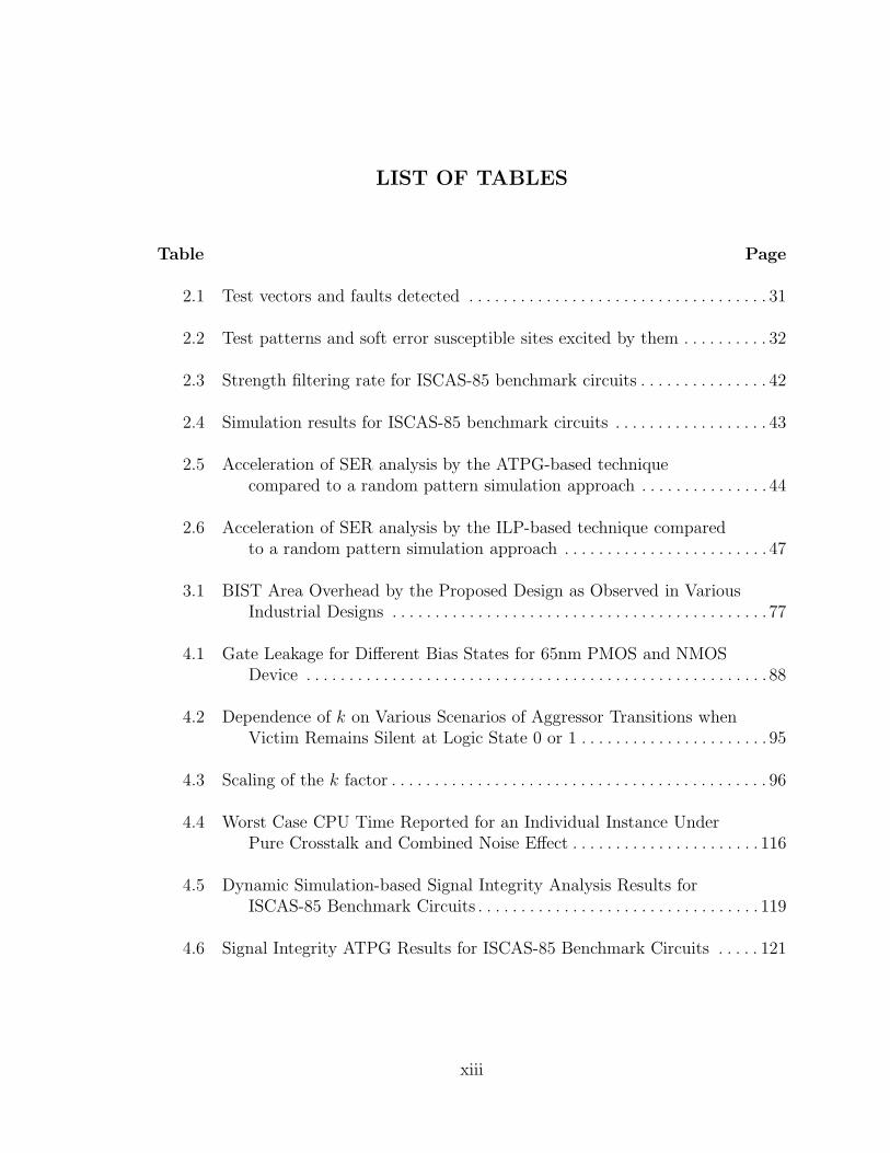
LIST OF TABLES
Table Page
2.1 Test vectors and faults detected . . . . . . . . . . . . . . . . . . . . . . . . . . . . . . . . . . . 31
2.2 Test patterns and soft error susceptible sites excited by them . . . . . . . . . . 32
2.3 Strength filtering rate for ISCAS-85 benchmark circuits . . . . . . . . . . . . . . . 42
2.4 Simulation results for ISCAS-85 benchmark circuits . . . . . . . . . . . . . . . . . . 43
2.5 Acceleration of SER analysis by the ATPG-based techniquecompared to a random pattern simulation approach . . . . . . . . . . . . . . . 44
2.6 Acceleration of SER analysis by the ILP-based technique comparedto a random pattern simulation approach . . . . . . . . . . . . . . . . . . . . . . . . 47
3.1 BIST Area Overhead by the Proposed Design as Observed in VariousIndustrial Designs . . . . . . . . . . . . . . . . . . . . . . . . . . . . . . . . . . . . . . . . . . . . 77
4.1 Gate Leakage for Different Bias States for 65nm PMOS and NMOSDevice . . . . . . . . . . . . . . . . . . . . . . . . . . . . . . . . . . . . . . . . . . . . . . . . . . . . . . 88
4.2 Dependence of k on Various Scenarios of Aggressor Transitions whenVictim Remains Silent at Logic State 0 or 1 . . . . . . . . . . . . . . . . . . . . . . 95
4.3 Scaling of the k factor . . . . . . . . . . . . . . . . . . . . . . . . . . . . . . . . . . . . . . . . . . . . 96
4.4 Worst Case CPU Time Reported for an Individual Instance UnderPure Crosstalk and Combined Noise Effect . . . . . . . . . . . . . . . . . . . . . . 116
4.5 Dynamic Simulation-based Signal Integrity Analysis Results forISCAS-85 Benchmark Circuits . . . . . . . . . . . . . . . . . . . . . . . . . . . . . . . . . 119
4.6 Signal Integrity ATPG Results for ISCAS-85 Benchmark Circuits . . . . . 121
xiii
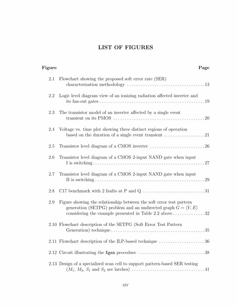
LIST OF FIGURES
Figure Page
2.1 Flowchart showing the proposed soft error rate (SER)characterization methodology . . . . . . . . . . . . . . . . . . . . . . . . . . . . . . . . . . 13
2.2 Logic level diagram view of an ionizing radiation affected inverter andits fan-out gates . . . . . . . . . . . . . . . . . . . . . . . . . . . . . . . . . . . . . . . . . . . . . . 19
2.3 The transistor model of an inverter affected by a single eventtransient on its PMOS . . . . . . . . . . . . . . . . . . . . . . . . . . . . . . . . . . . . . . . . 20
2.4 Voltage vs. time plot showing three distinct regions of operationbased on the duration of a single event transient . . . . . . . . . . . . . . . . . . 21
2.5 Transistor level diagram of a CMOS inverter . . . . . . . . . . . . . . . . . . . . . . . . 26
2.6 Transistor level diagram of a CMOS 2-input NAND gate when inputI is switching . . . . . . . . . . . . . . . . . . . . . . . . . . . . . . . . . . . . . . . . . . . . . . . . . 27
2.7 Transistor level diagram of a CMOS 2-input NAND gate when inputII is switching . . . . . . . . . . . . . . . . . . . . . . . . . . . . . . . . . . . . . . . . . . . . . . . . 29
2.8 C17 benchmark with 2 faults at P and Q . . . . . . . . . . . . . . . . . . . . . . . . . . . 31
2.9 Figure showing the relationship between the soft error test patterngeneration (SETPG) problem and an undirected graph G = 〈V,E〉considering the example presented in Table 2.2 above . . . . . . . . . . . . . . 32
2.10 Flowchart description of the SETPG (Soft Error Test PatternGeneration) technique . . . . . . . . . . . . . . . . . . . . . . . . . . . . . . . . . . . . . . . . . 35
2.11 Flowchart description of the ILP-based technique . . . . . . . . . . . . . . . . . . . . 36
2.12 Circuit illustrating the Xgen procedure . . . . . . . . . . . . . . . . . . . . . . . . . . . . . 38
2.13 Design of a specialized scan cell to support pattern-based SER testing(M1, M2, S1 and S2 are latches) . . . . . . . . . . . . . . . . . . . . . . . . . . . . . . . . 41
xiv

3.1 A modified architecture for the Pseudo Random Pattern Generator(PRPG) connected to multiple scan chains . . . . . . . . . . . . . . . . . . . . . . . 57
3.2 A modified architecture for the Multiple Input Signature Register(MISR) . . . . . . . . . . . . . . . . . . . . . . . . . . . . . . . . . . . . . . . . . . . . . . . . . . . . . 58
3.3 A waveform view of the control signals used in the PRPG and theMISR of the proposed architecture . . . . . . . . . . . . . . . . . . . . . . . . . . . . . . 60
3.4 Example showing improvement of testability by inserting: (a) controlpoint; and (b) observation point . . . . . . . . . . . . . . . . . . . . . . . . . . . . . . . . 62
3.5 (a) LFSR and phase shifter. (b) State transition matrix of theLFSR. . . . . . . . . . . . . . . . . . . . . . . . . . . . . . . . . . . . . . . . . . . . . . . . . . . . . . . 64
3.6 Example to illustrate the solution for a system of linear equations.(a) System of linear equations. (b) Gauss-Jordan elimination. (c)Solution space. . . . . . . . . . . . . . . . . . . . . . . . . . . . . . . . . . . . . . . . . . . . . . . . 65
3.7 Block diagram view of a distributed BIST process . . . . . . . . . . . . . . . . . . . . 67
3.8 Plot showing the principle of Fmax testing based on frequencyshmoo . . . . . . . . . . . . . . . . . . . . . . . . . . . . . . . . . . . . . . . . . . . . . . . . . . . . . . 70
3.9 A modified architecture for the Multiple Input Signature Register(MISR) . . . . . . . . . . . . . . . . . . . . . . . . . . . . . . . . . . . . . . . . . . . . . . . . . . . . . 72
3.10 A waveform view of the control signals used in the PRPG and theMISR of the proposed architecture . . . . . . . . . . . . . . . . . . . . . . . . . . . . . . 73
3.11 Frequency shmoo mechanism employed by the proposed BISTscheme . . . . . . . . . . . . . . . . . . . . . . . . . . . . . . . . . . . . . . . . . . . . . . . . . . . . . . 74
3.12 Scan path modifications to test thermal hotspot-induced transientfailures . . . . . . . . . . . . . . . . . . . . . . . . . . . . . . . . . . . . . . . . . . . . . . . . . . . . . . 76
4.1 Inertial and transport delay for a 2-input gate . . . . . . . . . . . . . . . . . . . . . . . 85
4.2 Illustration of signal integrity problem due to combined effect ofcapacitive crosstalk and loading on ISCAS-85 benchmark c17 . . . . . . . 86
4.3 Transistor terminal states considered in Table 4.1 . . . . . . . . . . . . . . . . . . . . 89
4.4 Gate leakage (left) and sub-threshold leakage (right) sensitivityversus loading effect in 45nm NMOS device . . . . . . . . . . . . . . . . . . . . . . 90
xv

4.5 Effect of loading current illustrated at gate level (left) and attransistor level (right) showing the bias states in the fanoutgates . . . . . . . . . . . . . . . . . . . . . . . . . . . . . . . . . . . . . . . . . . . . . . . . . . . . . . . . 91
4.6 Method to compute loading voltage in a cell using SPICE . . . . . . . . . . . . . 92
4.7 Illustration of an aggressor-victim model used for crosstalkanalysis . . . . . . . . . . . . . . . . . . . . . . . . . . . . . . . . . . . . . . . . . . . . . . . . . . . . . 94
4.8 Flowchart description of the dynamic simulation methodology . . . . . . . . . 99
4.9 C17 benchmark circuit with various switching times . . . . . . . . . . . . . . . . . 102
4.10 Circuit transformation of the ISCAS-85 benchmark C17 . . . . . . . . . . . . . 103
4.11 An example combinational logic block . . . . . . . . . . . . . . . . . . . . . . . . . . . . . 105
4.12 Illustration of gate leakage loading from fanout nodes of a victim Vat time slot tc . . . . . . . . . . . . . . . . . . . . . . . . . . . . . . . . . . . . . . . . . . . . . . . 109
4.13 Illustration showing the logic cones of interest for a typical instanceof the ATPG problem . . . . . . . . . . . . . . . . . . . . . . . . . . . . . . . . . . . . . . . . 115
4.14 Plot showing the worst CPU time taken by an individual instance ofthe ATPG for both cases of crosstalk and combined noiseeffect . . . . . . . . . . . . . . . . . . . . . . . . . . . . . . . . . . . . . . . . . . . . . . . . . . . . . . 116
6.1 An example illustrating the combined effect of power supply droopand crosstalk acting along a path P = 〈A,B,C,D,E〉 . . . . . . . . . . . . 126
xvi
CHAPTER 1
INTRODUCTION
The continuing trend of scaling transistor feature size driven by Moore’s law to
achieve greater density, higher performance and lower cost introduces several new
technology challenges in the context of both i〉 device, ii〉 design and iii〉 reliability
of ultra deep-submicron (UDSM) integrated circuits. The challenges in these three
domains are inter-twined in nature.
As we move deep into nanometric regime, power supply voltage (VDD) gets lowered
in accordance with the shrinking device dimensions, demanding for a proportionate
drop in device threshold voltage (VTH). Drop in power supply as well as device
threshold voltage together puts constraints on the design domain by causing i〉 an
exponential rise on leakage currents and ii〉 sharp erosion of noise margin. Constant
scale-up in circuit density coupled with scale-down in power supply voltage in every
successive technology generation also imposes dramatic increase in power and current
density across the chip. Moreover, non-uniform pattern of power consumption across
a power distribution grid causes a non-uniform voltage drop. Instantaneous switching
of nodes may cause localized drop in power supply voltage, known as droop causing
excessive delay and speed path problem. With every new technology generation the
slope of signal transition becomes sharper which introduces more noise and erodes
the noise margin further. In the nanometric regime of integrated circuits, the manu-
facturing technology itself introduces considerable process variation such as variation
in the i〉 device dimensions, and ii〉 inter-layer dielectric (ILD) thickness. Process
variation exacerbates the issues caused by erosion of noise margin further.
1
In the context of reliability of integrated circuits, highly eroded noise margin in-
creases the likelihood of transient failures (also known as parametric failures) during
device operation as compared to permanent failures introduced during manufacturing
process. A transient failure is the one which causes an incorrect logic state at the
output of a circuit node for a limited lifetime either i〉 due to impact of a high energy
particle on the device channel region, or ii〉 because of a specific Process-Voltage-
Temperature (PVT) condition being set up during the device operation. Since Com-
plimentary Metal Oxide Semiconductor (CMOS) is a restoring logic, the incorrect
logic state at the output of a node will eventually be replaced by the correct logic
state. However, during the limited time the incorrect logic state remains active, it
may propagate to an observable point in the circuit and may get recorded in a latch
manifesting as an error. Severity of such an error depends on the location of the error
on the processor datapath. We observe the following prominent sources of transient
failures in an integrated circuit:
1. Soft error: When a high-energy particle (such as i〉 an α-particle from radio-
active contaminants in packaging material, or ii〉 a high-energy neutron from
cosmic radiation, or iii〉 a high-energy proton from solar flare) impacts a semi-
conductor device surface, it gradually loses its kinetic energy while creating
electron-hole pairs (EHP) along its trajectory. The EHPs generated separate
promptly in presence of an electric field and a temporary inversion layer may be
created under the poly-silicon gate of a CMOS transistor. This produces a short
pulse of current with typical duration of 10-500 ps that may charge or discharge
an internal circuit node causing an incorrect logic state. This phenomenon is
known as a single event transient (SET). If this incorrect logic state propagates
to an observable point and gets recorded in a memory element then it causes a
single event upset (SEU) or soft error.
2

2. Capacitive cross-coupling related intermittent failure: Due to rapid
increase in circuit density and switching speed, input transitions in the neighbor
nets introduce significant voltage noise through parasitic capacitive coupling
between neighbors. The net which gets affected by this coupling noise is called
the victim and the coupled neighbor net whose signal transition causes the noise
is called an aggressor. The transient failure caused by this noise can be classified
into the following two categories:
i〉 Logic malfunction: when the logic state of the victim remains the same for
a given pair of input patterns, whereas signal transitions in the aggressor
nets introduce a coupling noise in the victim sufficient enough to alter its
logic state.
ii〉 Delay failure: when the victim and its aggressors switch in the opposite
directions for a given input pattern pair, the coupling noise introduced
in the victim causes a delay in signal transition which may eventually be
manifested as a failure at an observable output.
3. Thermal hot-spot induced delay failure: Large variations in power density
across the chip sometimes create thermal hot-spots in some functional units due
to localized overheating. In Metal Oxide Semiconductor (MOS) devices, there
are two parameters that are predominantly sensitive to temperature: i〉 the
carrier mobility µ; and ii〉 the device threshold voltage VTH . The mobility of
carriers in the channel is affected by temperature and a good approximation to
model this effect is given by [117]:
µ(T ) = µ(T0)(T
T0
)−k1 (1.1)
3
where T is the absolute temperature of the device, T0 is a reference absolute
temperature (usually room temperature) and k1 is a constant with values be-
tween 1.5 and 2 [56].
The device threshold voltage VTH exhibits a linear behavior with tempera-
ture [57]:
VTH(T ) = VTH(T0)− k2(T − T0) (1.2)
where the factor k2 is between 0.5mV/K and 4mV/K. The range becomes large
with more heavily doped substrates and thicker oxides.
Applying these considerations to the behavior of a MOS transistor, we can
predict that a temperature increment causes an increment of the drain current
due to the decrease in VTH and a decrease of the drain current due to decrease in
mobility. Among these two conflicting effects, the effect of mobility dominates
for circuits with large overdrive voltage (which is typically the case with ultra
deep sub-micron devices) resulting in slowing the devices in the thermal hot-
spot affected region of the chip, which may eventually manifest as an error at
an observable output.
4. Failure due to localized drop in power supply voltage: Rapid increase in
power density and operating frequency with every new technology generation
causes on-chip inductive drop (Ldidt
) along multilayer power grid that can no
longer be ignored [77]. Moreover, reduction of power supply voltage leads to
notable decrease in noise margin [27]. In this environment, when a logic gate
switches, it draws current from the power supply. If this current is large, then
a substantial voltage drop may occur at the nearest contact point (typically
the nearest M2-M3 supply via) to the power supply grid. This phenomenon
is known as droop. Due to this localized voltage drop, some other gates in
4

its vicinity, connected to the same M2-M3 via, may also experience significant
voltage drop. As a result, these gates may suffer from increased switching delay
which may eventually manifest as an error. Moreover, due to the distributive
and inductive nature of the power delivery network, certain other supply vias
in the vicinity of the droop-affected M2-M3 via may also experience significant
voltage drop and cause increased switching delay to the gates connected to these
vias as well.
In this thesis, we thoroughly investigate some of these transient failures, viz., i〉
single event upset or soft error; ii〉 capacitive cross-coupling related logic malfunctions;
and iii〉 thermal hot-spot induced delay failures. The measurement unit for soft errors
is Failure-in-Time (FIT) which represents number of soft errors encountered per
Billion hours of device operation. Given the time consuming nature of soft-error rate
(SER) measurement process, we propose an improved SER measurement technique in
Chapter 2, which accelerates the current state-of-the-art SER measurement process
by an order of magnitude. In Chapter 3, we propose a Built-In Self-Test (BIST)-based
technique for SER measurement that obviates the need for an external tester, thereby
greatly reducing the test cost. The proposed BIST architecture is a natural extension
of the existing BIST scheme employed for detecting permanent failures and retains
that capability with an added functionality of differentiating a permanent failure from
a transient failure. With a second application, we show that the proposed BIST may
also be used to detect thermal hot-spot induced delay failures. In Chapter 4, we
focus on capacitive cross-coupling related logic malfunctions, and through a dynamic
simulator-based study, first show that in nanometer design, increased gate leakage-
induced loading significantly erodes the noise margin for Bulk-CMOS and causes a
notably higher number of logic malfunctions when coupled with crosstalk related
noise. As a more comprehensive study of the combined effect of crosstalk and loading
as a potential cause for logic malfunctions, we develop an Integer Linear Program
5
(ILP)-based technique to generate test patterns that causes maximal circuit noise
due to crosstalk and loading. We conclude in Chapter 5, with a brief outline for
future research directions drawn from the scope of this thesis in Chapter 6.
6
CHAPTER 2
SOFT ERRORS AND IMPROVED MEASUREMENT
TECHNIQUES FOR SOFT ERROR RATE
2.1 Introduction
Soft-errors caused by ionizing radiation have emerged as a major concern for
current generation of technologies [11]. High energy neutrons from cosmic radiation
or α-particles from radioactive contaminants in packaging material creates electron-
hole pair in semiconductors. This electron-hole pair separates promptly in presence
of an electric field and a temporary inversion layer may be created under the gate of
a transistor. This produces a short pulse of current with typical duration of 10-500 ps
that may charge or discharge an internal circuit node used for logic computation. The
collected charge may be enough to alter the data state of a node [11, 45, 75]. If the
node is driven, as in the case of static CMOS, the node may recover quickly. If it is
a domino node, a register, latch, SRAM or any other type of memory cell, the wrong
value may persist until the node is written again.
Radioactive lead (210Pb →210 Bi →210 Po →206 Pb) in solder bumps was iden-
tified as a major source of soft-error and antique lead with isotopic separation was
identified to be a major cure. However, due to introduction of new materials into the
manufacturing process, soft-error cannot be tamed by changing packaging materials
alone. Some of the other known contaminants include 143Ce, 144Nd, 147Nd, 147Sm,
152Gd, 156Dy, 174Hf , 190Pt [9]. It has been established that soft error in semicon-
ductor devices is induced by three different types of radiation: α-particles [11,45,75];
high-energy neutrons from cosmic radiation [41, 131]; and/or the interaction of cos-
7

mic ray thermal neutrons and 10B in devices containing borophosphosilicate glass
(BPSG) [12, 85].
Shrinking power supply voltage is a major reason for rising soft-error rates. As
dynamic voltage scaling techniques get deployed more widely in the design process,
the charge generated by ionizing radiation will have greater destabilizing effect leading
invariably to greater rate for soft errors.
Shrinking dimensions lead to lower node capacitance making them more suscep-
tible to disruption due to charge generated by radiation. This is another contributor
to the rising rate of soft-error [84, 107].
Researchers have shown that Soft Error Rate (SER) in logic circuits is a significant
concern today [10]. It has been hypothesized that SER will increase by another nine
orders of magnitude from 1992 to 2011 and at that point will be comparable to
the SER per chip of unprotected memory elements [107]. It is also reported that
with decreasing supply voltage, highly pipelined deep-submicron CMOS circuits will
exhibit even higher soft error rate [51]. It is predicted that without adding error
protection mechanisms or a more robust technology (such as fully-depleted SOI), a
microprocessor’s error rate will grow in direct proportion to the number of devices
added to a processor in each succeeding generation [125].
It has been observed that all circuit nodes are not equally vulnerable to faults due
to soft errors [89]. Precisely, if the noise voltage produced at the output of a node
due to a particle hit becomes strong enough to overcome the minimum logic switching
threshold voltage [91,95] of all its fanout nodes only then the effect of the single event
transient propagates to the next level of the circuit. We term this approach of filtering
out nodes based on the ’strength’ of output noise voltage produced by a particle hit as
the strength filtering. Establishing the notion of strength filtering through MOSFET
equations is one of the primary contributions of this paper. To contribute to SER,
a single event transient (SET) must first be able to propagate to a memory element
8
and secondly it must reach this element during a clock cycle to be captured. In the
context of strength filtering, we focus only on logical propagation of an SET to an
observable output.
In this chapter, we address the issue of accelerating soft error rate (SER) test and
characterization using a two-pronged approach [100].
In the first step, we apply an efficient electrical analysis to obtain a reduced list
of SET-susceptible nodes that are rank ordered.
In the following step, we generate a set of test patterns with the characteristic
that each pattern should detect as many SETs as possible. It is a maximization
problem, the decision version of which falls under the NP-complete class. We present
two solutions to this computationally intractable problem of pattern generation: i〉
the first solution is based on a greedy heuristic; while ii〉 the second solution is based
on Integer Linear Programming (ILP).
The patterns are generated for combinational circuits. To enable application
of these patterns to sequential circuits we have also proposed design-for-testability
(DFT) architecture that permits test-per-clock to achieve the highest acceleration
possible.
2.2 Background and Related Work
2.2.1 The Soft Error Problem
The main causes of soft errors are α particles and low energy neutrons originating
from radioactive impurities in materials used in manufacturing.
When an α particle or a heavy ion strikes on a semiconductor device, its kinetic
energy is transferred into charge described by the linear energy transfer (LET) of the
particle [30]. As a result, a certain amount of free electrons and holes are created
(an order of 106 electron-hole-pairs is quoted in [87]). Other sources of soft-error are,
neutrons from nominal atmospheric radiation (energy level 1-10Mev), thermal neu-
9
trons (0.01ev-100Mev) produced from secondary sources, primarily from 10B isotope
found in p-type dopants and solar flare which is primarily a proton flux (500Mev)
that occurs every 11 years or so [9]. As mentioned earlier, soft error is caused by a
temporary inversion layer that is created by radiation which results in a voltage noise
on the line driven by the affected transistor.
A voltage noise of sufficient strength, i.e. a magnitude large enough to exceed
(or fall below) the logic threshold of a succeeding gate, can flip a node (introduce a
faulty logic value) for a limited amount of time. Such a noise is called a single event
transient (SET) [11]. A single event upset (SEU) occurs if the SET is propagated
to a primary output or a latch. A soft error is a direct consequence of an SEU. A
transient error in a logic circuit might not be captured in a memory circuit because
it could be filtered by one of the following three phenomena [107]:
Logical filtering occurs when a particle strikes a portion of the combinational
logic that is blocked from affecting the output due to a subsequent gate whose result
is determined solely by its other input values.
Latching window filtering occurs when the pulse resulting from a particle
strike reaches a latch, but is not present during clock transition when input values
are captured.
Electrical filtering occurs when the pulse resulting from a particle strike is
attenuated by subsequent logic gates to the point when it becomes inconsequential.
These filtering effects have been found to decrease the rate of soft errors in combi-
national logic compared to storage circuits in equivalent device technology [71]. How-
ever, these effects could diminish significantly as feature sizes decrease and number
of stages in the processor pipeline increases as mentioned earlier. Electrical filtering
could be reduced by device scaling because smaller transistors are faster and therefore
may have less attenuation effect on a pulse. Also, deeper processor pipelines lead to
higher clock rates, which may reduce latching-window filtering.
10

Estimation of SER on a soft error simulation model is compute intensive. The
computation of electrical filtering is significantly more expensive than the logic filter-
ing because the electrical filtering computation is performed in the SPICE level. With
our proposed approach we reduce the complexity of electrical filtering. We introduce
the concept of strength filtering that reduces the number of gates on which soft error
should be considered [101]. Thereafter the reduced set of soft-error susceptible nodes
are evaluated in subsequent pattern based soft error rate analysis methodology [98,99].
2.2.2 Failure-In-Time (FIT) Rate
The SEU frequency, which corresponds to the SER defined earlier, is typically
measured in Failures-In-Time (FIT), where 1 FIT is one failure per 109 device-hours.
The ITRS quotes 1 kFIT as a typical SER of modern products [48], while according
to [11] tens of kFITs are possible (100 kFIT is approximately one error per year).
It has been shown that not all single event transients contribute to failure [81]. In
this thesis, our objective is to cast as many single event transients at internal nodes
as single event upsets or detectable failures.
2.2.3 Factors Affecting the FIT Rate
The SER estimation should include a wide range of considerations, from the circuit
response to an injected charge up to architectural behaviors, which determine the
probability that an SEU would manifest itself as a system failure, wrong behavior, or
silent data corruption.
Three components make up the estimated FIT rate of a circuit element [84]:
Nominal FIT rate: The probability of an SEU occurring on a specific node. This
depends on circuit type, transistor sizes, node capacitance, VDD value, temperature,
and the downstream path in case of non-recycled circuits. It also depends on the
state of the inputs of the driving stage and the probability of each input vector, often
referred to as the signal probability of the circuit.
11
Timing Derating (TD): The fraction time in which the circuit is susceptible to
SEU that will be able to propagate and eventually impact a machine state.
Logic Derating (LD): The probability of an SEU to impact the behavior of the
machine. It is dependent on the applications as well as the micro-architecture of the
device.
2.2.4 Measurement of FIT Rate
The FIT rate of each element is given by the following equation:
FITelem = FITnominal × TD × LD (2.1)
Once the FIT rate of each element is determined, the chip FIT rate is the sum
of all the element FIT rates on die. Due to inherently low rate of failures, FIT rate
measurement is expensive. The options are i〉 testing a die for millions of hours or
ii〉 testing millions of dies concurrently for fewer hours or an iii〉 intermediate combi-
nation. While the first option is impractical, the second option is also prohibitively
expensive. Therefore much research has gone into acceleration techniques for soft-
error rate (SER) measurement. A known acceleration technique is to irradiate the
device to increase the soft error probability followed by measuring the accelerated soft
error rate (ASER). However, the SER-ASER conversion is inaccurate [58] and poorly
understood for combinational logic. Acceleration by lowering supply voltage is also
reported [105].
In this thesis, we propose the following two-pronged soft error rate (SER) charac-
terization methodology [100]:
Step I: estimation of SER for a given die through software simulation.
In the simulation environment, first faults are injected to a given circuit randomly
using a Poisson process [8] and input patterns are applied to compute the nominal
soft error rate (SERnominal). Next, the different soft error masking phenomena are
12
SET injection
(usingPoisson process)
FilterInput Pattern
Gate levelcircuit
description
SER estimation
Figure 2.1. Flowchart showing the proposed soft error rate (SER) characterizationmethodology
modeled as filter and applied to block the injection of faults to the circuit, which will
not have any impact in the circuit behavior. A specific set of input patterns is applied
to the primary inputs of the circuit, which especially excite the soft error susceptible
gates in their respective vulnerable state. The susceptible gates are the ones where
faults are injected after passing through the filters. The resulting accelerated soft error
rate (SERaccelerated) is noted. A flowchart visualization of this scheme is presented in
Figure 2.1. The ratio of the nominal and the accelerated soft error rate is posed as
the scaling factor (λ) in the following way:
λ =SERnominal
SERaccelerated(2.2)
A statistical requirement for computing this scaling factor is to keep the total
number of input patterns applied in both cases the same.
Step II: in-field measurement of SER for a fabricated die. The specific
set of input patterns obtained in the simulation step is applied repeatedly for few
iterations and the number of soft errors encountered is noted. This accelerated soft
13
error count is then appropriately scaled down by the factor λ obtained in step I to
report the actual soft error rate for a given die.
2.2.5 Related Work
The problem of soft error rate (SER) estimation has been studied in depth in
literature. Tosaka et al. measured SER of neutron-induced and α-particle induced
single event upsets through experiments [113,114] and observed that neutron-induced
soft errors were more frequent among the two. Several radiation hardening techniques
to reduce the soft error rate of high performance microprocessors have been proposed
by Weaver et al. [125], and V. Srinivasan et al. [110].
Soft error rate (SER) estimation is performed in different levels of abstraction. In
the circuit level, a SPICE-based simulation was first proposed by Baze et al. [13]. G.
R. Srinivasan et al. [109] later developed a Monte-Carlo simulation based computer
program (SEMM) to calculate the probability of soft errors in ICs due to α-particle
hit. Timing based simulators in the gate level were proposed by Cha et al. [17, 18].
A system level modeling and analysis-based approach was proposed by Zhang and
Shanbhag [130] which achieved an order of magnitude speed-up over Monte Carlo
based simulations with less than 5% error for computing the SER. However, their
probabilistic treatment of SER involves information extraction from chip layout. Fur-
thermore, the Soft Error Rate Analysis (SERA) technique proposed by the authors
involves conversion of a given circuit into an equivalent inverter chain followed by ap-
plying SPICE-based simulation on it as part of the main loop body of the algorithm.
These two steps drastically reduces the efficiency of the SERA algorithm when ap-
plied on large circuits. A recent work by Zhang, Wang and Orshansky [129] reported
a binary decision diagram (BDD)-based approach for SER analysis of cell-based de-
signs.
14
Several models have been proposed for logic filtering [25, 84], latching window
filtering [70] and electrical filtering [13] for accurately estimating the SER due to
particle strikes on combinational logic gates. Among them the Horowitz rise and
fall time model [43] to determine the rise and fall time of the output pulse, and the
logical delay degradation effect model [14] to determine the amplitude and hence the
duration of the output pulse, are of special importance in the context of electrical
filtering. Mohanram [80] proposed a logical effort [111]-based closed form linear RC
model for computing the noise voltage produced by single event transient. Gill et
al. [39] considered all the paths from a node to an observable output and expressed
the sensitivity of the node as a product of three factors: the SEU rate of the node, the
probability that the pulse is not logically masked, and the ratio of latching window
to the clock cycle. The sensitivity of the node was defined as the maximum over
all paths from the given node. A similar soft-error tolerance analysis composed as a
function of three masking effects was reported by Dhillon et al. [28]. Wang et al. [122]
recently proposed an improved transient pulse generation and propagation model to
model the electrical masking effect more accurately.
Soft error rate measured by accelerating the test by controlling the external en-
vironment has significant shortcomings as mentioned earlier [58]. Among various
methods of SER estimation studied in literature over a decade, there is not enough
work reported on the test pattern generation problem for detecting soft errors and
estimating SER in integrated circuits by specifically targeting the soft error suscep-
tible nodes in a circuit. Krishnaswami et. al. [60] proposed a probabilistic soft error
detectability measure and composed a matrix to express the detection probability of
all the circuit nodes followed by using it to generate test sets to detect soft errors.
Polian et al. [89] characterized soft errors by formally defining the impact of a tran-
sient fault in terms of three basic parameters: frequency, observability and severity.
They showed that, using these parameters, online architecture for transient fault de-
15

tection and diagnosis can be optimized to meet multiple objectives, such as ensuring
minimum fault detection probabilities, and identifying fault modes on the fly. In
that paper, it was proposed that repeating the same pattern may be the best way
to accelerate SER testing. However, in this thesis we present a discussion in section
V to show that this conjecture may not necessarily be true if manufacturing process
variation is taken into account.
2.3 Node Vulnerability
A single event transient (SET) occurs if the total charge Q deposited by the
particle exceeds the critical charge Qcrit of the node in question. The value of Qcrit
is typically measured through circuit simulation [84].
The vulnerability of a node from transient errors is primarily a combination of the
following three factors:
Strength of the output capacitance: A node is more likely to discharge when
it stores less charge. Therefore, the weaker the node capacitance, more vulnerable it
is to soft errors. Also, scaling the supply voltage VDD will decrease the Qcrit value
of a given node thereby increasing the vulnerability of the node. Voltage scaling is
related to both technology scaling as well as power management techniques [105].
Strength of the pull-up network: In CMOS circuits, all data nodes are driven.
Suppose a node is driven by the pull-up network. If the pull-up network is considerably
weaker than the pull-down network, an SET on the pull-down path of the node may
flip a logic value of 1 temporarily. During this time the node behavior can be modeled
as a stuck-at-0 fault. For the purpose of this paper we refer to this situation as 1-
vulnerability.
Strength of the pull-down network: Similarly, if the pull-down network is
considerably weaker than the pull-up network an SET on the pull-up path of the
16

node may temporarily flip a logic value of 0. Likewise we refer to this situation as
0-vulnerability.
For CMOS circuits, vulnerability of the nodes can be determined by simulation or
by computation using mathematical expressions. In the following section, we derive
closed form mathematical expressions for determining vulnerability.
2.4 Strength Filtering-based Preprocessing
In a general scenario, the gates may have different strengths for pull-up and pull-
down paths. Consequently the switching threshold which is defined as the point where
input voltage equals output voltage may be different for different gates. Convention-
ally switching threshold voltage is considered to be the point where the input signal
is distinguished from logical 0 to logical 1.
2.4.1 Problem Definition
Suppose a node is driven to a logic value 0 and an SET in the pull-up path intro-
duces a positive voltage noise. The fanout gates of this node may or may not interpret
this voltage noise as an error depending on their switching threshold voltages. Our
definition of strength filtering is rooted in this concept.
Definition 1: A node G is considered to be filtered in the context of 0-vulnerability if
the positive noise voltage produced by the single event transient (SET) on the output
of that node is less than the minimum logic switching threshold voltage of any of its
fanout gates.
Mathematically:
SF (G)|0 = Vout −min(Vswi) ∀i ∈ F (G) (2.3)
17
where Vout represents the output noise voltage of the SET-affected node G, F (G)
is the set of all fanout nodes of G and Vswirepresents the logic switching threshold
of the ith fanout gate of G.
Now the necessary and sufficient condition for strength filtering in the context of
0-vulnerability for node G is:
SF (G)|0 ≤ 0 (2.4)
On the other hand, if SF (G)|0 > 0, then the node G is considered vulnerable for
an appropriate single event transient and all such nodes are recorded in a potential
list of soft errors along with the magnitude of SF (G)|0 as the real valued vulnerability
weight for the given soft error affected node. From ATPG perspective, we simply call
it a weighted fault list. The subsequent soft error rate (SER) estimation techniques
take this weighted fault list as an input and generate test patterns that specifically
target these set of vulnerable nodes. The detailed description of these test pattern
generation techniques are presented in Sections 2.6 and 2.7.
The necessary and sufficient condition for strength filtering in the context of 1-
vulnerability for a node G can be defined in a very similar way and has been omitted
for the sake of brevity.
Before delving into details of the mathematical derivation for Vout and Vsw for
different gates, let us consider the following example illustrating the notion of strength
filtering in the context of 0-vulnerability.
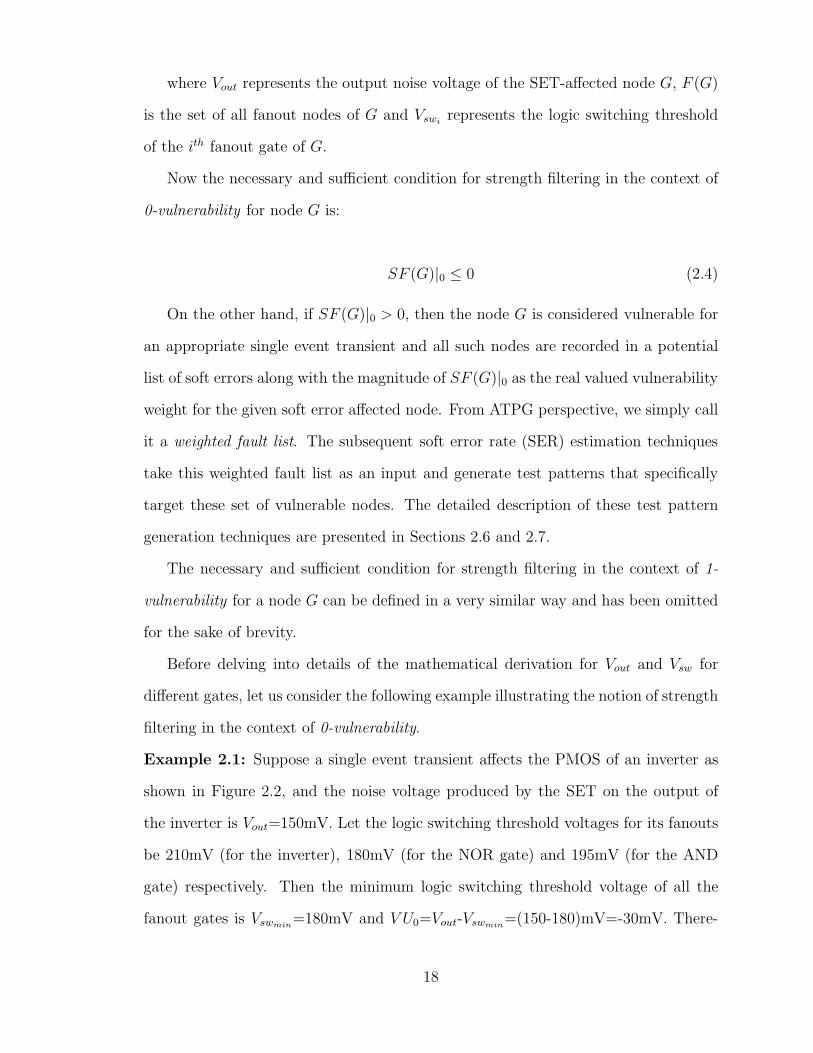
Example 2.1: Suppose a single event transient affects the PMOS of an inverter as
shown in Figure 2.2, and the noise voltage produced by the SET on the output of
the inverter is Vout=150mV. Let the logic switching threshold voltages for its fanouts
be 210mV (for the inverter), 180mV (for the NOR gate) and 195mV (for the AND
gate) respectively. Then the minimum logic switching threshold voltage of all the
fanout gates is Vswmin=180mV and V U0=Vout-Vswmin
=(150-180)mV=-30mV. There-
18
ionizingradiation Vout
Figure 2.2. Logic level diagram view of an ionizing radiation affected inverter andits fan-out gates
fore, according to the condition described in equation (2), the SET occurring in the
inverter will not manifest at the output of its fanout gates. Such an SET merits no
further consideration for soft error analysis purposes. According to our definition and
procedure this gate will be strength filtered in the context of 0-vulnerability. �
With the above discussion on definition of strength filtering, we now focus on de-
riving closed form expressions for the two principle parameters, viz. Vout and Vsw of
the equation (2.3) in the following two subsections. First we illustrate the computa-
tion of Vout on inverter. Here we assume that PMOS is impacted by SET. Then we
derive Vsw for inverter and 2-input NAND gate to illustrate the procedure for deriva-
tion of switching threshold. Our derivations are based on Sakurai-Newton α-power
law model [95]. This model is more accurate than the conventional square-law model
for short channel MOSFETs.
In this paper, our purpose is to establish the notion of strength filtering in the
context of single event transient. Here we derive the closed form expressions for Vout
and Vsw.
2.4.2 Derivation of Closed Form Expression for Vout
Following notations have been used in the rest of the derivation:
19

ionizingradiation Vout
0
1
0
I’DOp
I’DOn
C L
outi
Figure 2.3. The transistor model of an inverter affected by a single event transienton its PMOS
VDD : supply voltage
VTH : threshold voltage of a MOS transistor
VTp, VTn
: threshold voltage of PMOS/NMOS
µp, µn : PMOS and NMOS mobility
ǫox : permittivity of SiO2
tox : thickness of the gate oxide
Wp, Wn : PMOS and NMOS transistor width
Leff : effective channel length of PMOS/NMOS
α : velocity saturation index
VDO : drain sat. voltage at VGS = VDD
IDO : drain current at VGS = VDS = VDD
In the following derivation we assume the threshold voltage for PMOS (VTp) and
NMOS (VTn) are not equal in magnitude.
When a single event transient happens in the PMOS of an inverter with a steady
state output voltage of logic 0, the PMOS temporarily gets turned on for a finite
duration of time This duration was assumed to be ∼50ps in [89, 99]. The inverter
20

Vol
tage
Time
Region I Region II Region III
t 2 t 3
t 1
Figure 2.4. Voltage vs. time plot showing three distinct regions of operation basedon the duration of a single event transient
behavior during this period can be approximated by the model shown in Figure 2.3,
where the PMOS is driven by an input logic 0 and the NMOS is driven by the natural
input (which is set to logic 1).
By analyzing the device behavior for the above model, we identify three distinct
regions of operation based on the duration of single event transient (Figure 2.4):
Region I: when Vout < |VTp|, the PMOS would be saturation region and the NMOS
would be in linear region
Region II: when |VTp| ≤ Vout ≤ VDD − VTn
, both the PMOS and the NMOS would
be in linear region
Region III: when Vout ≥ VTn, the PMOS would be in linear region and the NMOS
would be in saturation region.
The computation of output noise pulse height involves the following three steps:
1. Analytical expressions for boundary time constants t1, t2 and t3 (Figure 2.4)
which partition the device behavior under the effect of single event transient
into the above three regions is computed in the following way:
21

(a) The expression for the node current iout is derived under the condition of
SET
(b) iout substituted by CLdVout
dt
(c) Finally, integration is performed w.r.t. t by applying the limiting voltage
conditions as specified above
2. The actual values of these time constants t1, t2 and t3 are computed by ap-
propriately substituting the values of the device parameters involved in the
expressions for a given CMOS technology.
3. Once the duration of the SET is known, which region(s) the device will operate
on is identified instantly, and based on that the output noise voltage (Vout) is
computed.
The rest of the sub-section deals with a more formal mathematical treatment for
deriving analytical expressions for the boundary time constants t1, t2 and t3.
Region I: When Vout < |VTp|: the PMOS would be in saturation region and the
NMOS would be in linear region. We use Sakurai-Newton α-power law model [95]
which expresses the drain current (ID) of a MOS transistor by considering the carrier
velocity saturation effect in the following way:
ID =
0 (VGS ≤ VTH : cut− off region)
(I ′DO/V′
DO)VDS (VDS < V ′
DO : triode region)
I ′DO (VDS ≥ V ′
DO : pentode region)
(2.5)
where
I ′DO = IDO(VGS − VTH
VDD − VTH
)α (2.6a)
V ′
DO = VDO(VGS − VTH
VDD − VTH)α/2 (2.6b)
22

With the drain current (ID) defined above, the equation for the output current
(iout) for a single event transient (SET)-affected node is expressed below:
iout = I ′DOp−I ′DOn
V ′
DOn
VDSn(2.7)
where,
I ′DOp=
1
2k1(VDD − |VTp
|)2(VGSp
− |VTp|
VDD − |VTp|)α (2.8a)
I ′DOn=
1
2k2(VDD − VTn
)2(VGSn
− VTn
VDD − VTn
)α/2 (2.8b)
with
k1 = µpǫox
tox
·Wp
Leff
(2.9a)
k2 = µnǫox
tox·Wn
Leff(2.9b)
Substituting iout with CLdVout
dtand integrating with the boundary condition for
Vout = |VTp| we obtain the time expression:
t1 =2VDO
k2(VDD − VTn)2ln|
X
X − Y| (2.10)
where,
X =1
2k1(VDD − |VTp
|)2(−VDD − |VTp
|
VDD − |VTp|
)α (2.11a)
Y =1
2k1(VDD − VTn
)2 VTp
VDO(2.11b)
Region II: When |VTp| ≤ Vout ≤ VDD − VTn
: both the PMOS and the NMOS would
be in linear region and the expression for iout would be:
23

iout = (I ′DOp
V ′
DOp
)VDSp− (
I ′DOn
V ′
DOn
)VDSn(2.12)
Expanding the terms of the above equation, we get:
iout = ip − in (2.13)
where,
ip =1
2k1(VDD − |VTp
|)2(VGSp
− |VTp|
VDD − |VTp|)α/2VDSp
VDO
(2.14a)
in =1
2k2(VDD − VTn
)2(VGSn
− VTn
VDD − VTn
)α/2VDSn
VDO(2.14b)
Integrating in a similar way by applying the proper boundary conditions for Vout
we obtain:
t2 = t1 + ln|N(VDD − VTn
)− VDD
VDO
N |VTp| − VDD
VDO
| (2.15a)
N =1
VDO
[X −1
2k2(VDD − VTn
)2] (2.15b)
using the expression for X from equation (10a).
Region III: When Vout ≥ VTn: the PMOS would be in linear region and the NMOS
would be in saturation region and the expression for iout would be:
iout = (I ′DOp
V ′
DOp
)VDSp− I ′DOn
(2.16)
Similarly expanding the terms of the above equation, we get:
iout = ip −1
2k2(VDD − VTn
)2(VGSn
− VTn
VDD − VTn
)α (2.17)
The expression for time t3 would be obtained as:
24

t3 = t2 + C · ln|X · VDD −
VDD
VDO
X(VDD − VTn)− VDD
VDO
| (2.18)
using the expression for X from equation (10a).
As mentioned earlier, the time constants t1, t2 and t3 (equations 9, 14a and 17
respectively) are used to determine the region in which the model works in order to
compute the output noise voltage (Vout) of the SET-affected gate given the duration
of the single event transient.
2.4.3 Closed Form Expression for Logic Switching Threshold Voltage
With the above analysis on the computation of Vout, we now derive the closed
form expressions for the logic switching threshold voltage of different gates.
Definition 2: The logic switching threshold voltage of any gate G, is defined as the
input voltage when it becomes equal to the output voltage of the gate in the process of
transition from one logic value to another.
Using the above definition, we now derive the logic threshold of inverter and 2-
input NAND gate by equating the PMOS drain current and the NMOS drain current,
when both are in the saturation region.
Under the condition VGS = VDS = VDD, the expressions for IDOpand IDOn
are
given below:
IDOp=
1
2k1(VGSp
− |VTp|)2 =
1
2k1(VDD − |VTp
|)2 (2.19)
and,
IDOn=
1
2k2(VGSn
− VTn)2 =
1
2k2(VDD − VTn
)2 (2.20)
25

Vin VoutC L
Figure 2.5. Transistor level diagram of a CMOS inverter
2.4.3.1 Logic Switching Threshold for Inverter
Equating the drain current of the PMOS and the NMOS of an inverter (Figure 2.5)
in the saturation region, we get:
IDOp(VGSp
− |VTp|
VDD − |VTp|)α = IDOn
(VGSn
− VTn
VDD − VTn
)α (2.21)
Expanding the terms of the equation above, we obtain:
1
2k1 · B
2(Vlt − VDD − |VTp
|
VDD − |VTp|
)α =1
2k2 · A
2(Vlt − VTn
VDD − VTn
)α (2.22)
where,
A = VDD − VTn(2.23a)
B = VDD − |VTp| (2.23b)
Solving equation (21),we obtain the logic threshold of inverter as:
VltINV=C1 · VTn
− C2 · VDD − C2 · |VTp|
C1 − C2(2.24)
where,
26
0
Vsw
1
Vout
vC L
Figure 2.6. Transistor level diagram of a CMOS 2-input NAND gate when input Iis switching
C1 = k1/α2 · A2/α · B (2.25a)
C2 = k1/α1 · A · B2/α (2.25b)
2.4.3.2 Logic threshold for 2-input NAND gate
There are two distinct cases involved with the derivation of logic threshold for a
2-input NAND gate.
Case I: When the input is connected to the upper NMOS in the stack (Figure 2.6),
the expression for logic threshold is derived as follows:
Let the voltage between two NMOS transistors in stack be v (see Figure 2.6).
When the input 1 switches from voltage 0 to a voltage Vlt (the logic threshold voltage),
the PMOS and the NMOS connected to the switching input will both be in saturation
region and the other NMOS (closer to ground rail) will be in linear region.
Therefore,
27

I ′DOp= I ′DOn
(2.26)
Expanding the parameters involved in the above equation we get:
1
2k1 · B
2(Vlt − VDD − |VTp
|
VDD − |VTp|
)α =1
2k2 · A
2(Vlt − v − VTn
VDD − VTn
)α (2.27)
Again,
I ′DOp=I ′DOn
V ′
DOn
VDSn(2.28)
Expanding the parameters involved in the above equation we get:
1
2k1 · B
2(Vlt − VDD − |VTp
|
VDD − |VTp|
)α =1
2k2 · A
2 ·v
VDO(2.29)
Solving equations (26) and (28) for Vlt, we get:
V 1ltNAND
=VDD(C3 · VTn
− C2)− |VTp|(C3 · VTn
+ C2)
C3 · (VDD−VTp)− C2
(2.30)
where the term C2 has been presented in equation (24b) and C3 is defined as
follows:
C3 = k1/α2 · A2/α (2.31)
The expression for V 1ltNAND
refers to the logic switching threshold voltage for case
I.
Case II: When the input connected to the lower NMOS in the stack switches (Fig-
ure 2.7), the expression for logic switching threshold, V 2ltNAND
, may be derived in a
similar way as explained for case I above.
The application of the electrical filtering described above significantly reduces the
number of potential SET sites for which test patterns should be generated.
28

Vout
vC L
1
0
Vsw
Figure 2.7. Transistor level diagram of a CMOS 2-input NAND gate when input IIis switching
This filtering approach has been applied on ISCAS-85 benchmark circuits to iden-
tify which gates are vulnerable. The result is reported in Section 2.9.1.
2.5 The Test Pattern Generation Problem
In the previous section, we have established that not all soft errors are equally
likely. Therefore, targeting patterns that go after most likely soft errors will achieve
the highest acceleration. Suppose, we have n potential soft error sites with varying
likelihood of occurrence. Then the broad objective of the test pattern generation
problem should be to find a single test pattern that maximizes the cumulative prob-
ability of occurrence of soft error by taking into account all the potential soft error
sites with varying likelihood of occurrence. This problem was touched upon by Po-
lian et al. [89] However, in reality, one test may not be able to detect all stuck-at
faults. In that case, the test generation objective should be to maximize the overall
vulnerability weight of a given circuit with least number of test patterns.
To clarify the reasoning behind applying more than one test pattern to a given
circuit, let us assume two soft errors f1 and f2 with f1 having a higher occurrence
29
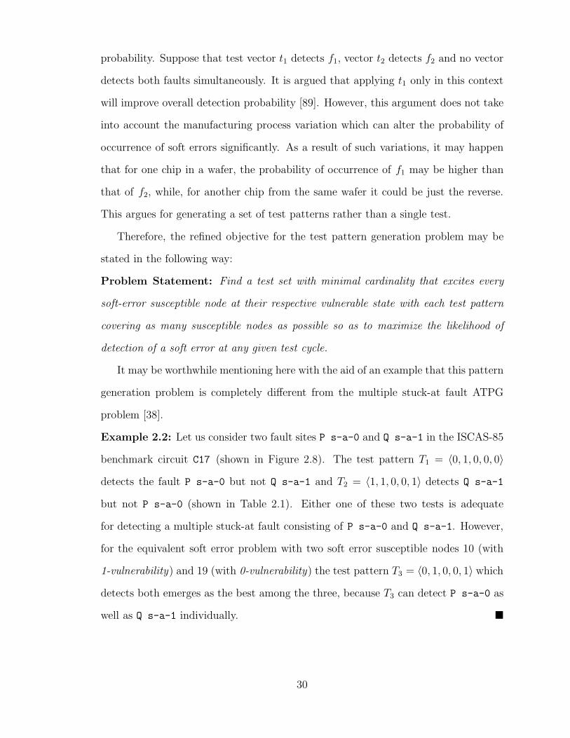
probability. Suppose that test vector t1 detects f1, vector t2 detects f2 and no vector
detects both faults simultaneously. It is argued that applying t1 only in this context
will improve overall detection probability [89]. However, this argument does not take
into account the manufacturing process variation which can alter the probability of
occurrence of soft errors significantly. As a result of such variations, it may happen
that for one chip in a wafer, the probability of occurrence of f1 may be higher than
that of f2, while, for another chip from the same wafer it could be just the reverse.
This argues for generating a set of test patterns rather than a single test.
Therefore, the refined objective for the test pattern generation problem may be
stated in the following way:
Problem Statement: Find a test set with minimal cardinality that excites every
soft-error susceptible node at their respective vulnerable state with each test pattern
covering as many susceptible nodes as possible so as to maximize the likelihood of
detection of a soft error at any given test cycle.
It may be worthwhile mentioning here with the aid of an example that this pattern
generation problem is completely different from the multiple stuck-at fault ATPG
problem [38].
Example 2.2: Let us consider two fault sites P s-a-0 and Q s-a-1 in the ISCAS-85
benchmark circuit C17 (shown in Figure 2.8). The test pattern T1 = 〈0, 1, 0, 0, 0〉
detects the fault P s-a-0 but not Q s-a-1 and T2 = 〈1, 1, 0, 0, 1〉 detects Q s-a-1
but not P s-a-0 (shown in Table 2.1). Either one of these two tests is adequate
for detecting a multiple stuck-at fault consisting of P s-a-0 and Q s-a-1. However,
for the equivalent soft error problem with two soft error susceptible nodes 10 (with
1-vulnerability) and 19 (with 0-vulnerability) the test pattern T3 = 〈0, 1, 0, 0, 1〉 which
detects both emerges as the best among the three, because T3 can detect P s-a-0 as
well as Q s-a-1 individually. �
30

101
s−a−0
P
3
2
7
6
22
Q
s−a−1
16
19
23
11
Figure 2.8. C17 benchmark with 2 faults at P and Q
Test vector Location P Location Q(s-a-0) (s-a-1)
T1 = 〈0, 1, 0, 0, 0〉 YES NOT2 = 〈1, 1, 0, 0, 1〉 NO YEST3 = 〈0, 1, 0, 0, 1〉 YES YES
Table 2.1. Test vectors and faults detected
With the above discussion on the soft error test pattern generation problem, we
now analyze the complexity of this problem with the aid of the following theorem:
Theorem: The decision version of the soft error test pattern generation problem is
NP-complete.
Proof: The language representing the decision version of the soft error test pattern
generation (SETPG) problem can be formally stated in the following way:
L = {〈T, k〉 : the test set T has a subset of k tests
which can excite the entire set of soft error
susceptible sites for a given circuit C}
To prove that L is NP-complete, we have to prove the following [23]:
i〉 L ∈ NP , and
31

Test Fault sites excitedt1 f1, f2
t2 f1, f4
t3 f1, f3
t4 f2, f3
t5 f2
Table 2.2. Test patterns and soft error susceptible sites excited by them
t1
t2
t3
t4
t5
f
f
f
f
f1
1
1
2
3
4f
Figure 2.9. Figure showing the relationship between the soft error test patterngeneration (SETPG) problem and an undirected graph G = 〈V,E〉 considering theexample presented in Table 2.2 above
ii〉 L′ ≤p L for every language L′ ∈ NP
Lemma I: L ∈ NP : We provide a two input algorithm A1 which, given an instance
of the language L and k test patterns from a test set T , verifies whether these test
patterns can excite the entire set of soft error susceptible sites for a given circuit
C. We clearly see that the algorithm A1 functions in linear time with the size of k.
Therefore, the language L is verifiable in polynomial time.
Hence, L ∈ NP .
Lemma II: L′ ≤p L: To prove the NP-completeness of the language L, we have
to show that every language L′ ∈ NP is polynomially reducible to the language L.
In other words, it will suffice to show the polynomial time reducibility of a known
NP-complete problem to the given language L since an NP-complete problem is an
universal representative of the entire NP class.
32

We choose the VERTEX-COVER problem as the known NP-complete problem in
this case by observing its striking similarity with the given language L representing
the SETPG problem. The language representing the VERTEX-COVER problem is
formally stated as follows:
L′ = {〈G, k〉 : graph G has a vertex cover of size k}
We define the following polynomial time algorithm A2 which computes the reduc-
tion function f mapping every instance x ∈ L′ to an instance f(x) ∈ L:
1. Every single vertex v ∈ V for G = 〈V,E〉 is mapped to a corresponding vertex
tı ∈ T for the constructed graph G′ representing the language L.
2. If there is an edge (u, v) ∈ E for G = 〈V,E〉 and u 7→ tı and v 7→ t, then
(tı, t) ∈ E′ where E ′ is the edge set of the constructed graph G′.
In the constructed graph G′ = 〈T,E ′〉, an edge (tı, t) ∈ E′ implies that both test
patterns tı and t excite some common soft error susceptible site fs in a given circuit
C. Now if we find a subset of vertices T ′ ⊂ T (with |T ′| = k) in the constructed graph
G′ representing the language L, which excites the entire set of soft error susceptible
sites for a given circuit C (in other words, covers all the edges of the constructed
graph G′), we may immediately conclude that the original graph G representing the
language L′ for the VERTEX-COVER problem has a cover of size k. Therefore, the
language L is not more than a polynomial factor harder than the known NP-complete
language L′ representing the VERTEX-COVER problem.
Hence, L′ ≤p L.
From lemma I and lemma II we conclude that the language L representing the
decision version of the soft error test pattern generation (SETPG) problem is NP-
complete. �
33

In the following two sections, we present two solutions to this computationally
intractable problem of pattern generation: the first solution is based on i〉 a greedy
heuristic, while the second solution is based on ii〉 Integer Linear Programming (ILP).
2.6 Automatic Test Pattern Generation-based Technique
With the above discussion on the soft error ATPG problem, we now describe our
first pattern generation technique based on a greedy heuristic.
We start with the list of vulnerable nodes which were identified with a real-valued
vulnerability weight associated with each of them through the strength filtering-based
preprocessing of a given circuit as described in Section 2.4.
A node suffering from 0-vulnerability (1-vulnerability) is equivalent to saying the
output of the node is stuck at 1 (0). Test patterns are generated using a combi-
national ATPG tool. X’s in the patterns are filled randomly and simulated until
additional benefits are not found for a fixed number of consecutive iterations, called
step size. Patterns are chosen by a greedy algorithm that favors a pattern that detects
faults with highest accumulated vulnerability, with a ’no-fault-drop’ simulator until
a minimum number of patterns are found to detect all faults or a subset of faults
that achieve vulnerability goals. A flow chart description of the algorithm is shown
in Figure 2.10.
The simulation results of this greedy heuristic on ISCAS-85 benchmark circuits is
presented in Section 2.9.2.
While the greedy approach is fast, it is not always optimal. Next, we present
an Integer Linear Programming (ILP) based technique that is computationally more
intensive but seeks to find a near-optimal solution.
34
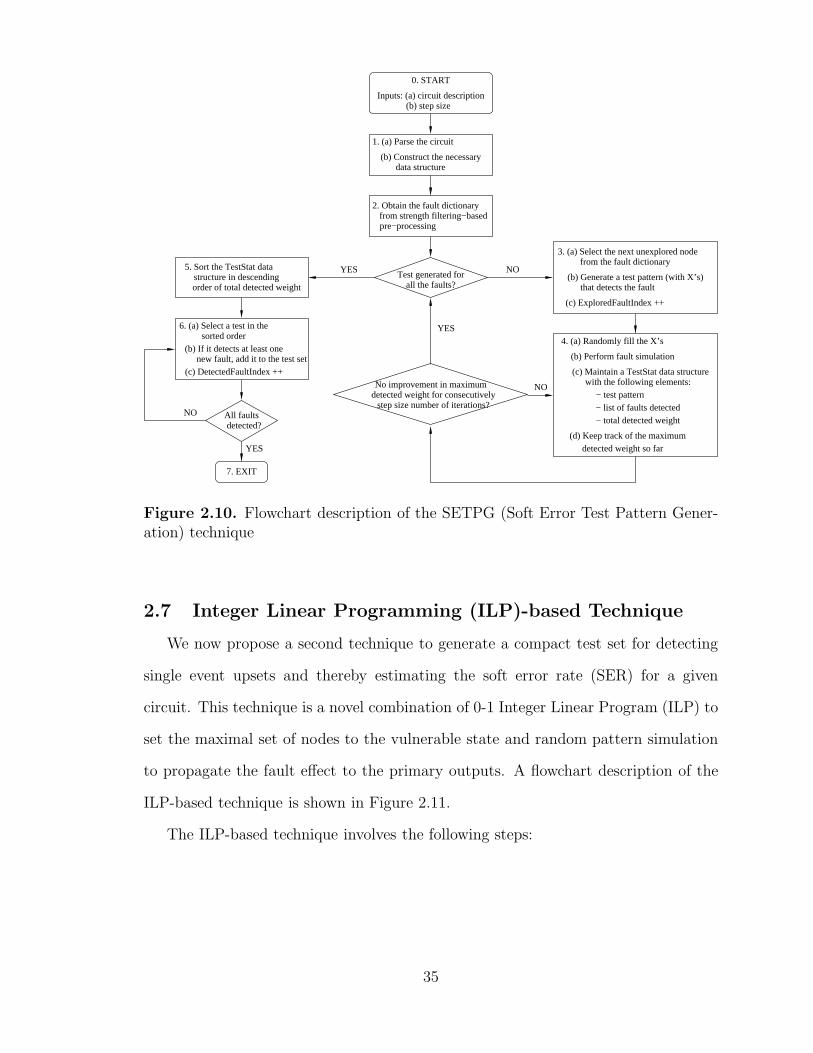
(b) step sizeInputs: (a) circuit description
0. START
1. (a) Parse the circuit
(b) Construct the necessarydata structure
2. Obtain the fault dictionary
pre−processingfrom strength filtering−based
Test generated forall the faults?
4. (a) Randomly fill the X’s
(b) Perform fault simulation
(c) Maintain a TestStat data structurewith the following elements:
− test pattern
(d) Keep track of the maximumdetected weight so far
− list of faults detected− total detected weight
3. (a) Select the next unexplored nodefrom the fault dictionary
(b) Generate a test pattern (with X’s)that detects the fault
(c) ExploredFaultIndex ++
step size number of iterations?detected weight for consecutivelyNo improvement in maximum
5. Sort the TestStat datastructure in descendingorder of total detected weight
sorted order
new fault, add it to the test set
6. (a) Select a test in the
(b) If it detects at least one
(c) DetectedFaultIndex ++
All faultsdetected?
7. EXIT
NOYES
YES
YES
NO
NO
Figure 2.10. Flowchart description of the SETPG (Soft Error Test Pattern Gener-ation) technique
2.7 Integer Linear Programming (ILP)-based Technique
We now propose a second technique to generate a compact test set for detecting
single event upsets and thereby estimating the soft error rate (SER) for a given
circuit. This technique is a novel combination of 0-1 Integer Linear Program (ILP) to
set the maximal set of nodes to the vulnerable state and random pattern simulation
to propagate the fault effect to the primary outputs. A flowchart description of the
ILP-based technique is shown in Figure 2.11.
The ILP-based technique involves the following steps:
35

1. ILP FORMULATION
0. STARTInput: circuit description
(c) Write an objective function invlovingthis subset in the aim of maximizing it
(b) Select a subset of vulnerable nodes
terms of linear equations(a) express functinality of logic gates in
2. DON’T CARE GENERATION (XGEN)
Generate don’t cares on some specified primary
− from the fault sites along the input cone− assigning X to non−controlling inputs of gates
inputs (PI) using backtrace reasoning :
3. FAULT EFFECT PROPAGATION
(a) Set the don’t cares (X’s) in the PIs andomly to eitherlogic 0 or logic 1 state
(b) Compute the total weight of the list of faults detected
(c) Continue STEP 3 till we reach a local maximum in thecontext of total detected weight
(d) Maintain a TestStat data structure with followingelements:
− test pattern− list of faults detected
Remove the detected faults with minimumvulnerability weight from the fault list
list empty?Is the fault
END
NO
YES
Figure 2.11. Flowchart description of the ILP-based technique
36

2.7.1 ILP Formulation
In order to set the maximal set of suspect nodes in the vulnerable state, ILP
formulation is done by writing the linear equations for the logic gates. The ILP
equations of the gates are formed by using the clausal description of the function of
the gates given in [66]. For example, for a AND gate with inputs a, b and output c,
we can describe all the 4 input-output combinations as given below:
a⇒ c or a + (1− c) ≥ 1 (2.32a)
b⇒ c or b+ (1− c) ≥ 1 (2.32b)
ab⇒ c or (1− a) + (1− b) + c ≥ 1 (2.32c)
a, b, c ∈ [0, 1] (2.32d)
Other logic gates can similarly be described by ILP equations. The objective
function is a sum of product of the suspect node outputs and the corresponding node
vulnerability weight. For example if the binary variables x1, x2 and x3 corresponding
to the suspect nodes have vulnerabilities 0, 1 and 1 and weights 0.5, 0.8 and 0.6 then
the objective function is given below:
Maximize: Obj = (1− x1) · 0.5 + x2 · 0.8 + x3 · 0.6 (2.33)
While a satisfying input assignment for the above objective function guarantees that
the respective soft error sites are excited in their vulnerable state, it does not guar-
antee propagation of the fault effect(s) to an observable point. We discuss next how
we deal with this problem.
37

10 22
16
19
23
11
i1
i3
i6
i2
i7
X
X
X
0
1
1
11
1 1X
1
0
X 0
X X 1
X
00
Figure 2.12. Circuit illustrating the Xgen procedure
2.7.2 Don’t Care Generation (Xgen)
Unfortunately, patterns produced by ILP are often over-specified which causes
problem for subsequent ATPG step. We solve this problem by turning some specified
inputs to Xs. The actual procedure for doing so is illustrated with an example below.
Example 2.3: In the circuit below, assume that the nodes 22 and 23 are the
0-vulnerable. ILP formulation for nodes 22 and 23 results in an input pattern
(〈i1, i2, i3, i6, i7〉 = 〈0, 1, 1, 0, 0〉) as shown in Figure 2.12.
Backtrace from node 22 along the input logic cone and assigning X to non-
controlling inputs we get the input pattern 〈X, 1, X, 0, 0〉. For example, the non-
controlling value 1 at the input (gate 10) of gate 22 is turned to an X. This X at the
output of the gate 10 makes both its inputs X. We can see that for the gate 16 with
output at 0, both the input values are required. Now doing backtrace starting at
node 23 and assigning an X to all the nodes which are not at a required or controlling
values results in a pattern 〈X, 1, X, 0, X〉. As a result the original pattern 〈0, 1, 1, 0, 0〉
was turned to 〈X, 1, X, 0, X〉. �
38
Thus the Xgen was able to introduce 3 don’t cares by identifying the minimum set
of primary inputs which should be assigned a specific logic value to set the suspect
nodes in vulnerable state.
2.7.3 Fault Effect Propagation
After determining the pattern that sets a maximal set of nodes to the vulnerable
value, we need to specify logic values for don’t cares in the input pattern so as to
propagate the maximal set of these faulty values to the primary output(s) simulta-
neously. For a given pattern with X’s (obtained from Xgen), these don’t cares are
randomly assigned 0 or 1 and the resulting pattern is applied to the primary inputs
of the circuit to compute the total weight of all the fault effects propagated to the
primary outputs(s). For a given pattern with X’s, this process of random assignment
of logic value 0/1 to the unspecified inputs is continued till we reach a local maximum
on total detected weight. We keep track of this pattern with the list of faults detected
by maintaining a TestStat data structure before moving to the next pattern with
X’s.
The above three steps are performed in the given order. To get higher fault
coverage we seek to generate more patterns so as to cover the faults not covered yet.
In the next iteration of the pattern generation algorithm, the nodes with minimum
weight among the vulnerable nodes that are excited are eliminated form the fault list.
This action changes the targets for fault effect propagation. The algorithm terminates
when all the nodes are excluded, thus generating a test set with a size equal to the
length of the fault list.
2.8 Design-For-Testability to Facilitate SER Measurement
Sequential test pattern generation is known to be a complex problem. Therefore,
the proposed pattern generation methods are based on a scan architecture. In scan-
39
based testing, a large fraction of the total test application time is spent idle during
the shift operation. To improve efficiency of scan-based testing we propose a design-
for-testability (DFT) architecture that allows test-per-clock scheme.
The basic procedure involves shifting in the scan pattern into scan cells where
it will be stored in a latch, followed by applying that pattern in every clock cycle
during the SER test mode. When the functional clock is applied, the output(s) of the
combinational circuit, including any error, needs to be captured into a master latch.
To enable counting of the number of errors, the contents of the master latch should
be scanned out to an external pin. Since soft errors are rare events, we further assume
that while an error from one SEU is in the scan chain, another error is highly unlikely.
Thus the scan cell should have the ability to shift during the SER test cycles. In the
context of system debug, such scan cells have been used in industrial designs [64].
Our DFT architecture is a variant of the full hold-scan approach [64] that supports
the following modes:
1. Functional mode: In this mode the circuit should be able to function with
little to no performance overhead.
2. Scan mode: It allows shifting in scan patterns onto the functional master and
slave latches for test purposes.
3. Shift during SER testing: In this mode, the captured data is shifted through
the scan chain. Since we have a test-per-clock scheme, new test data appears in
every clock that needs to be convolved with result from prior cycles. In order
to enable this scheme, we turn the entire scan chain into a long multiple input
signature register (MISR) [20] without feedback. The errors that appear at the
output can be counted by a tester or with small modification by on-die circuitry.
40
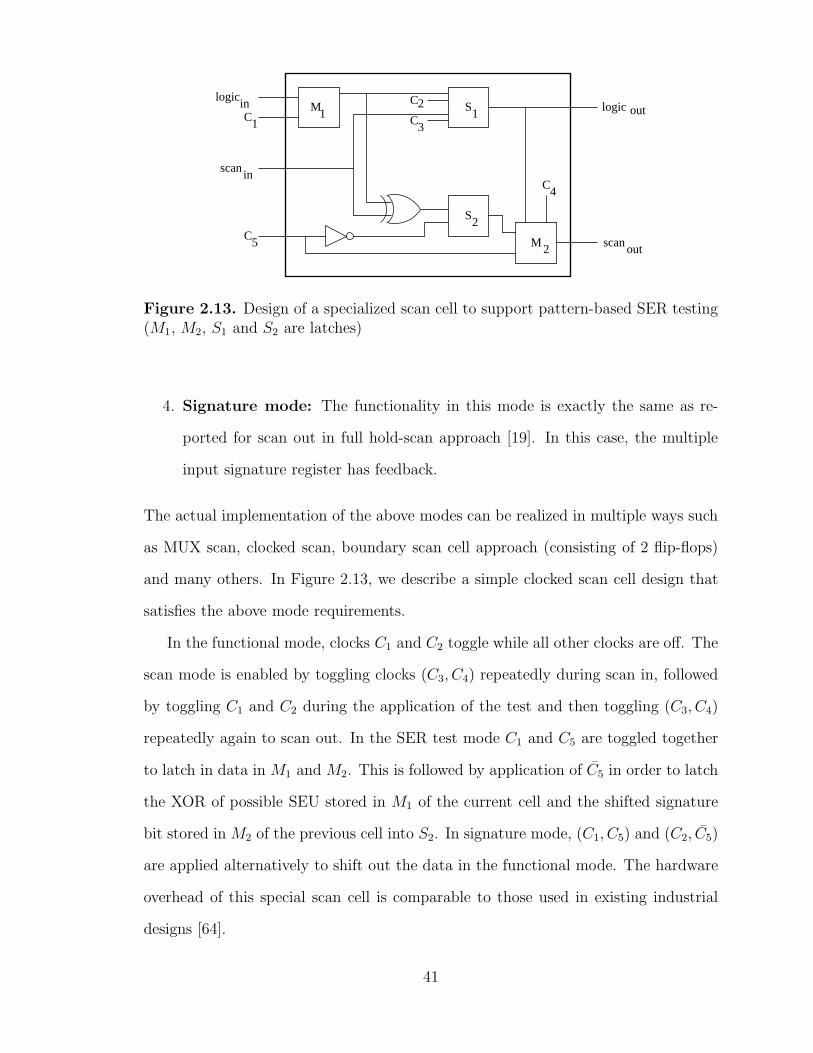
M1
M
2S
2
1SC1
C
C2
3
C
C
4
5
logic
scan
in
out
inscan
logicout
Figure 2.13. Design of a specialized scan cell to support pattern-based SER testing(M1, M2, S1 and S2 are latches)
4. Signature mode: The functionality in this mode is exactly the same as re-
ported for scan out in full hold-scan approach [19]. In this case, the multiple
input signature register has feedback.
The actual implementation of the above modes can be realized in multiple ways such
as MUX scan, clocked scan, boundary scan cell approach (consisting of 2 flip-flops)
and many others. In Figure 2.13, we describe a simple clocked scan cell design that
satisfies the above mode requirements.
In the functional mode, clocks C1 and C2 toggle while all other clocks are off. The
scan mode is enabled by toggling clocks (C3, C4) repeatedly during scan in, followed
by toggling C1 and C2 during the application of the test and then toggling (C3, C4)
repeatedly again to scan out. In the SER test mode C1 and C5 are toggled together
to latch in data in M1 and M2. This is followed by application of C5 in order to latch
the XOR of possible SEU stored in M1 of the current cell and the shifted signature
bit stored in M2 of the previous cell into S2. In signature mode, (C1, C5) and (C2, C5)
are applied alternatively to shift out the data in the functional mode. The hardware
overhead of this special scan cell is comparable to those used in existing industrial
designs [64].
41
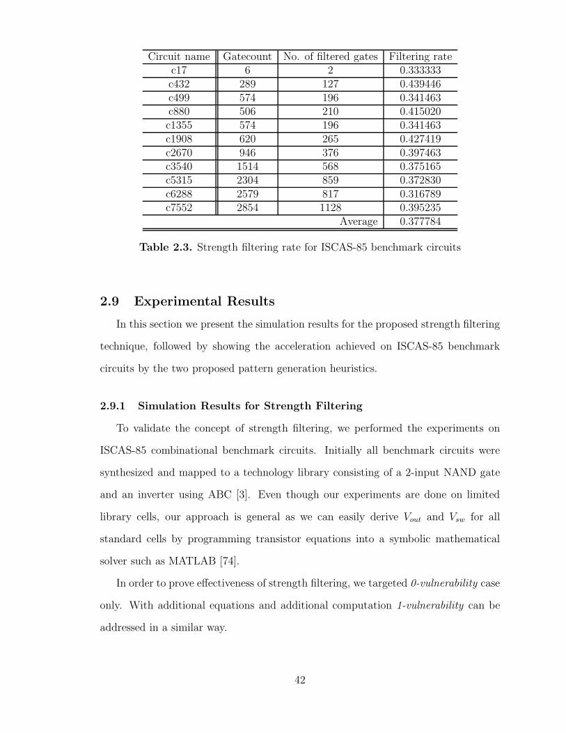
Circuit name Gatecount No. of filtered gates Filtering ratec17 6 2 0.333333c432 289 127 0.439446c499 574 196 0.341463c880 506 210 0.415020c1355 574 196 0.341463c1908 620 265 0.427419c2670 946 376 0.397463c3540 1514 568 0.375165c5315 2304 859 0.372830c6288 2579 817 0.316789c7552 2854 1128 0.395235
Average 0.377784
Table 2.3. Strength filtering rate for ISCAS-85 benchmark circuits
2.9 Experimental Results
In this section we present the simulation results for the proposed strength filtering
technique, followed by showing the acceleration achieved on ISCAS-85 benchmark
circuits by the two proposed pattern generation heuristics.
2.9.1 Simulation Results for Strength Filtering
To validate the concept of strength filtering, we performed the experiments on
ISCAS-85 combinational benchmark circuits. Initially all benchmark circuits were
synthesized and mapped to a technology library consisting of a 2-input NAND gate
and an inverter using ABC [3]. Even though our experiments are done on limited
library cells, our approach is general as we can easily derive Vout and Vsw for all
standard cells by programming transistor equations into a symbolic mathematical
solver such as MATLAB [74].
In order to prove effectiveness of strength filtering, we targeted 0-vulnerability case
only. With additional equations and additional computation 1-vulnerability can be
addressed in a similar way.
42

Circuit total number Fault Cardinalityname of gates dictionary size of the test setc17 6 0 -c432 160 2 1c499 202 4 3c880 383 11 3c1355 546 16 5c1908 880 23 7c2670 1193 38 14c3540 1669 51 20c5315 2307 70 17c6288 2416 73 8c7552 3512 107 23
Table 2.4. Simulation results for ISCAS-85 benchmark circuits
First we determine the output noise voltage level due to single event transient
(SET) using equations derived in Section 2.4.2. Next we derive the switching thresh-
old corresponding to every input of a gate using equations described in Section 2.4.3.
Following the derivations of output noise voltage and input logic switching threshold
the filtering process described in Section 2.4.1 was used to reduce the number of SETs
that have no potential impact. The results from experiments conducted on ISCAS-85
benchmark circuits are shown in Table 2.3.
As the results indicate, an average of ∼38% of the SETs have no potential im-
pact as observed by taking driver sizing, output load and switching threshold into
consideration as explained in detail in Section 2.4.
Thus the strength filtering technique is significant in two ways: i〉 it improves the
soft error rate estimation process at the system level; and ii〉 during accelerated soft
error testing the patterns can be targeted for manifestable soft errors only, thereby
improving the accelerated SER testing method significantly.
43
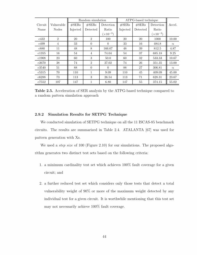
Random simulation ATPG-based technique
Circuit Vulnerable #SERs #SERs Detection #SERs #SERs Detection Accel.
Name Nodes Injected Detected Ratio Injected Detected Ratio
(×10−3) (×10−3)
c432 2 20 2 100 20 20 1000 10.00
c499 4 33 0 0 33 16 484.8 ∝
c880 11 48 8 166.67 48 39 812.5 4.87
c1355 16 54 4 74.04 54 37 685.18 9.25
c1908 23 60 3 50.0 60 32 533.33 10.67
c2670 38 74 2 27.02 74 26 351.35 13.00
c3540 51 88 0 0 88 27 306.81 ∝
c5315 70 110 1 9.09 110 45 409.09 45.00
c6288 73 113 3 26.54 113 71 628.31 23.67
c7552 107 147 1 6.80 147 55 374.15 55.02
Table 2.5. Acceleration of SER analysis by the ATPG-based technique compared toa random pattern simulation approach
2.9.2 Simulation Results for SETPG Technique
We conducted simulation of SETPG technique on all the 11 ISCAS-85 benchmark
circuits. The results are summarized in Table 2.4. ATALANTA [67] was used for
pattern generation with Xs.
We used a step size of 100 (Figure 2.10) for our simulations. The proposed algo-
rithm generates two distinct test sets based on the following criteria:
1. a minimum cardinality test set which achieves 100% fault coverage for a given
circuit; and
2. a further reduced test set which considers only those tests that detect a total
vulnerability weight of 90% or more of the maximum weight detected by any
individual test for a given circuit. It is worthwhile mentioning that this test set
may not necessarily achieve 100% fault coverage.
44

The effectiveness of the patterns obtained from the ATPG-based technique is mea-
sured by comparing its soft error detection rate to that obtained from the random
patterns.
SETs are typically modeled as a Poisson process with an average arrival rate of
λ faults per simulation second [8]. We used this process to inject soft-error into our
target circuits.
From the ATPG-based approach, we obtain a test set which consists of a set of
patterns and the associated total detected vulnerability weight. A pattern in the test
set is applied for the duration proportional to the weight it detects. The number of
repetitions of the test set is such that a total of 10,000 test vectors are applied. The
same procedure is followed with random patterns except that the test set consists of
10,000 random patterns which are applied one by one for the same duration without
repetition. The simulation is run for a time limit of 1,000,000 simulation seconds.
Single event transients (SET) are injected only at the susceptible nodes and the
average arrival rates (i.e. the Poisson parameter λ) at different susceptible nodes is
set in proportion to their vulnerability weights thus reflecting the actual SER analysis
environment.
Table 2.5 shows the acceleration reported for this ATPG-based technique on
ISCAS-85 benchmarks over random pattern testing. In this case, a minimum car-
dinality test set which achieves 100% fault coverage was used. As evident from Ta-
ble 2.5 the acceleration achieved by SETPG algorithm ranges from 5X to 55X with
an average acceleration of 21X (on finite set) over random pattern SER measurement.
Note that the acceleration was computed on the basis of the random vulnerability
weights assumed for different gates and the average was calculated only for the cases
that gave a finite acceleration. Infinite acceleration was obtained for circuits c3540
and c499 where the random pattern test set did not detect any fault. We observe a
45
trend that our algorithm achieves higher acceleration with larger circuits (e.g. the
highest acceleration of 55X achieved for c7552).
2.9.3 Simulation Results for ILP-based Technique
The effectiveness of the patterns obtained from the ILP-based heuristic is mea-
sured by comparing its SER detection rate to that obtained from the random patterns.
The arrival process of SETs is typically modeled as a Poisson process with an average
fault rate of λ [8].
From the ILP-based technique we obtain a test set consisting of a set of patterns
and a set of associated weights that the pattern excites. These patterns are applied
one by one for time duration varying in proportion to the associated weight it excites.
This test set was applied repeatedly for 10,000 times, to accelerate the SER detection
rate. The same procedure is followed with random patters except that we apply
100,000 random patters without repetition. The above numbers are chosen such that
they are large enough to get a good statistics. The simulation is run for a time limit
of 1000,000 simulation seconds.
Faults are only injected at the suspect nodes and the average fault arrival rate of
different suspect nodes is set in proportion to their vulnerability weight with maxi-
mum value of 0.2 arrivals per second, which gives one SER fault for 8 patterns thus
mimicking the actual SER test process.
Table 2.6 shows the results obtained from random pattern SER simulation and
SER simulation for the patterns generated from the ILP-based technique. Table 2.6
also compares the two approaches and shows the acceleration obtained for the ILP-
based approach. It can be seen in the Table 2.6 that the average SER acceleration
obtained is 5.252 with highest acceleration obtained for the circuits like C2670 and
C3540.
46

Random simulation ILP-based technique
Circuit Vulnerable Total Total Detection Total Total Detection
Name Nodes #SERs #SERs ratio #SERs #SERs ratio Accel.
Injected Detected (×10−3) Injected Detected (×10−3)
c17 4 20138 1291 63.96 20188 5358 265.4 4.15
c432 11 24397 30 1.23 23499 102 4.341 3.53
c499 10 24095 37 1.536 23382 138 5.92 3.85
c880 11 24180 87 3.598 24134 221 9.15 2.54
c1355 11 24589 20 0.813 25044 131 5.23 6.43
c1908 8 24412 98 4.041 24422 661 27.06 6.70
c2670 11 24588 14 0.569 24138 131 5.24 9.21
c3540 11 23160 27 1.16 22649 214 9.44 8.14
c5315 7 23880 364 15.24 23737 1165 56.18 3.69
c7552 11 24117 30 1.244 24439 130 5.32 4.28
Table 2.6. Acceleration of SER analysis by the ILP-based technique compared to arandom pattern simulation approach
To obtain the above results, the proposed ILP-based technique was run on a Dell
PowerEdge 2800 server with 2.8GHz Dual Core Intel Xeon Processor, 2MB L2 cache
and 2GB RAM. ILP problem was solved using GLPK, a GNU Linear Programming
Kit [55]. A workload consisting of all the circuits ran in less than an hour except for
the circuit c6288 which becomes a complex problem.
2.10 Conclusions and Future Directions
In this chapter, we presented an improved measurement technique for soft error
rate characterization. In the first step, we proposed a strength filtering technique
based on electrical analysis to obtain a subset of circuit nodes that are potentially
affected by single event transients (SET). The strength filtering technique further
allows us to rank the likelihood of SETs with a weighted measure. A smaller list of
target nodes and intelligent pattern generation techniques that have been presented
in this paper significantly increases the probability that if a soft error occurs it will be
detected. This has been corroborated by our experimental results which show that
47
on an average 37.78% of the nodes can be eliminated from consideration, while the
pattern generation techniques improve soft error detectability by an average factor
of 21X for the greedy heuristic and 5X for the ILP-based technique, which combined
together produces a total improvement of 11.0−0.38
× 21.43 = 34.56X in accelerating
SER testing.
The charge particles have a wide distribution in energy and consequently varying
effects on SET. This can only be captured by probabilistic filtering methods which
remains an open problem and a subject of our future investigation.
48
CHAPTER 3
BUILT-IN SELF-TEST FOR DETECTION AND
CHARACTERIZATION OF TRANSIENT ANDPARAMETRIC FAILURES
3.1 Introduction
The continuing trend of scaling transistor feature size to achieve greater density,
higher performance and lower cost introduces several new technology issues in nano-
scale CMOS integrated circuits. Constant scale-up in circuit density coupled with
scale-down in power supply voltage in every successive technology generation imposes
dramatic increase in power and current density across the chip. Moreover, non-
uniform pattern of power consumption across a power distribution grid causes a non-
uniform voltage drop. Instantaneous switching of nodes may cause localized drop
in power supply voltage, known as droop. This instantaneous drop in power supply
grid at the point of switching causes excessive delay and speed path problem [112].
With every new technology generation the slope of signal transition becomes sharper.
Resulting increase in noise, coupled with lower supply voltage, sharply erodes noise
margin. In this environment, manufacturing process variation, such as inter-layer
dielectric thickness (ILD) variation that can introduce greater noise due to crosstalk
effects, may cause failure [62]. Influence of one or more of these effects together cause
logic malfunction and delay failures at specific Process-Voltage-Temperature (PVT)
conditions. The trend toward failure from such parametric variations is on the rise
as opposed to the permanent failures caused by physical defects introduced during
manufacturing process.
49
Different sources of parametric variations, also called circuit marginality issues,
broadly encompass three distinct effects [63]: i〉 process approximations: this category
includes a number of design parameter related issues. Process files used in design are
rarely in sync with the actual process because actual process itself is a moving target,
while parameter file is a relatively static entity; ii〉 design approximations: current
generation design process involves multiple levels of hierarchy at logical, circuit and
physical levels to deal with exponential growth in design size. This compromises
accuracy at many levels including the interconnect resistance-capacitance (RC) ex-
traction process because global interconnects may span across multiple entities in
a physical design hierarchy; and iii〉 time-to-market: with an explosive number of
checking tools (crosstalk, IR droop, electro-migration, to name a few), the number of
design violations that are flagged is very large. Most of these violations tend to be
false negatives and are due to overly simplifying assumptions in the checking tools
themselves. Designers often ignore these violations to be in the market on time even
though these violations often provide a leading clue on potential circuit marginality
related failures.
Automatic test pattern generation (ATPG) for testing various transient failures
requires an accurate fault model which often becomes fairly complex to deal with.
Moreover, a large number of patterns are needed to test these failures under varied
voltage and temperature conditions. A tester-based approach to detect transient
errors typically suffers from the following problems: i〉 scan testing requires a large
number of test cycles leading to a significant increase in test application time and
cost; and also ii〉 functional testing requires functional pattern generation - a problem
that remains largely unsolved to date.
Another class of transient failures are due to impact of high energy particles (such
as, α-particle, high energy proton from solar flare or high energy neutron from radio-
active contaminants) on semiconductor surface. When a high energy particle impacts
50
a semiconductor surface and traverses through the substrate, it generates electron-
hole pairs (EHP) in the process of losing its kinetic energy. The electron and the hole
quickly get separated in the presence of body bias, and may accidentally form a con-
ducting channel below the gate for a short duration. This causes a noise pulse, called
single event transient (SET). If the SET gets propagated to an observation point,
it manifests as an error, called single event upset or soft-error. Shrinking device di-
mension coupled with constant scale-down in power supply voltage also aggravate the
soft-error problem. Therefore, for nano-CMOS technology, accurate characterization
of soft-error rate (SER) is an important design concern. Testing for accurate SER
measurement in integrated circuits poses a significant challenge. The unit of SER
measurement, Failure-in-Time (FIT), where 1 FIT is one failure per billion device-
hours, inherently complicates SER testing as, metaphorically, either a single device
needs to be tested for billion hours or a billion devices needs to be tested for an hour.
The practical approach in solving the SER measurement problem is to test multiple
devices in parallel to reduce both test time and cost.
Using built-in hardware feature, such as a built-in self-test (BIST) engine, is a
natural choice for enabling parallel test environment suitable not only for SER testing,
but for testing other kinds of circuit marginality related transient failures as well. A
BIST-based test methodology also provides an important advantage in dissociating a
tester from the test process. It is particularly important in the context of radiation-
accelerated SER measurement environments (such as neutron beam testing), where
it is difficult to bring in cumbersome testers in the vicinity of radiation chamber.
However, BIST architecture and functionalities need to be tailored for accurate
detection and isolation of transient failures from any permanent fail during testing.
Particularly, the soft error rate measurement can be further benefited in a BIST-based
approach by applying targeted patterns that can selectively exercise a set of SET-
susceptible nodes in a circuit [89, 99]. Although the test time for SER measurement
51
is inherently long in any test method, BIST-based approach can yet significantly aid
testing in mission critical applications in multiple ways. BIST-based SER testing
can lead to test cost reduction due to more efficient tests, less expensive tester and
test equipments, parallel testing, and improved error detection and accumulation in
BIST. Despite these potential benefits, BIST-based SER testing, particularly BIST
architectural techniques for efficient and accurate characterization of SER have not
been addressed adequately in literature to date. In this thesis, we present a novel
linear feedback shift register (LFSR) and multiple input signature register (MISR)-
based Built-In Self-Test (BIST) architecture [96, 97] for soft error rate measurement
and SER characterization, facilitating parallel testing of multiple devices via network
controller.
We also show that a very similar architecture, without significant modification,
may also be used to detect other kinds of intermittent failures, such as those caused
by increased delay due to temperature effects (also known as thermal hot-spot induced
delay failure) [97, 102].
In the following two sections we present a novel BIST-based scheme and its ap-
plications in the context of detection and characterization of soft-errors and thermal
hot-spot induced delay failures. The overhead and cost-benefit analysis of the pro-
posed scheme are presented in Sections 3.4 and 3.5. We conclude in Section 3.6.
3.2 Application I – Soft Error Rate Characterization
3.2.1 Background and Related Work
The existing literature related to the problem of occurrence of soft error and its
estimation can be broadly classified into the following two categories: i〉 analytical
techniques for predicting likelihood of a single event upset (or soft error) and predict-
ing the rate at which a system might fail relative to the occurrence of single events;
and ii〉 SER measurement systems for test chips. Tosaka et al. [114] and Karnik et
52

al. [53] describe α-particle and neutron induced SER measurement and analysis using
test chips and accelerated test environments. Srinivasan et al. [109] developed a com-
prehensive computer program to calculate the probability of soft errors in ICs due to
α-particle hit. A modeling and analysis-based approach was proposed by Zhang and
Shanbhag [130], which achieved an order of magnitude speed-up over Monte Carlo
based simulations with less than 5% error for computing the SER.
The factors associated with technology scaling that impacts soft error susceptibil-
ity in integrated circuits are: i〉 shrinking device dimensions, ii〉 reduced capacitance
at internal nodes, ii〉 increased number of nodes and devices, and iv〉 reduced design
margin due to lower supply voltage and higher performance requirements. A variety
of techniques in all levels - process technology, circuit design, and architectural design,
exist to reduce and maintain SER of a chip within its FIT budget [81]. Techniques
to reduce the soft error rate of high performance microprocessors were reported by
Weaver et al. [125]. On-line testing techniques to detect occurrence of a soft fail is
necessary to enable architectural solutions like single bit correction and double bit
detection via Error Correction Code (ECC), and operational retry procedures after
concurrent detection [76,123]. Operational retry is also utilized by Yilmaz et al. [127]
to test soft vs. hard fail in fault tolerance mechanisms implemented in a multiplier
with the aid of redundant hardware. Built-in current sensing techniques are proposed
for on-line detection of errors in memory arrays [116,119] as well as logic circuits [115].
In addition to SER testing in test-chips for process optimization and device char-
acterization [53, 114], SER testing and characterization in product chips would also
be essential for two primary reasons. Firstly, in mission critical applications, such as
biomedical, automotive, aerospace, and defense, a better measure of SER is desirable
by testing product chips rather than simple test chips to qualify them to be within
SER budget. Secondly, SER testing can quantify the effectiveness of the previously
mentioned on-line soft error detection and correction techniques [76,115,116,119,123,
53
127] that are integral part of functional circuits in the product chips. SER testing for
product chips would require BIST circuits and methodology to reduce test cost and
time.
Although there are in-depth studies on analytical methods to predict SER [109,
130], or radiation-hardened design techniques [76, 79, 115, 116, 119, 123, 127], there is
hardly any published literature on built-in SER measurement systems. Given that
soft errors are more prevalent in memories, Kushida et al. [65] proposed a design-for-
testability technique to implement ECC for memory arrays such that the entire ECC
system along check-bit array can be tested with memory BIST. Polian et al. [89] re-
cently proposed an online, non-concurrent BIST architecture for characterizing tran-
sient faults in dynamic noisy environments. Their online test scheme stores a set of
pre-defined test vectors and their fault-free responses. The test vectors are applied
continuously to an idle block to detect the occurrence of a possible transient fault.
However, this deterministic online test scheme suffers from the following problems:
i〉 a system with half-a-million flip-flops will require half-a-million bits in an on-chip
ROM, which will be expensive; ii〉 explicit X-masking will be required for such a
deterministic pattern ATPG, which will grow design complexity and area overhead
further; and finally iii〉 a deterministic ATPG does not address the manufacturing
process variation, as the generated patterns target only a pre-defined set of single
event transient (SET) susceptible nodes.
In this section, we describe a linear feedback shift register (LFSR) and multiple-
input signature register (MISR)-based BIST architecture for accurate SER measure-
ment. Although major architectural elements in BIST technique for SER measure-
ment is similar to those used in conventional LFSR/MISR-based BIST [5], an impor-
tant additional capability in BIST for SER measurement is its ability to distinguish
between soft and hard fails for accurate SER counting. BIST for SER measurement
54
will therefore consist of all conventional BIST elements with addition of soft fail
identification, and hence, can also be used as conventional BIST to test hard fails.
3.2.2 The Proposed Architecture
Built-in self-test (BIST) is a design-for-testability (DFT) technique in which test-
ing (test generation and test application) is accomplished through built-in hardware
features [5]. Built-in self-test applied in scan environment significantly improves the
controllability and observability of a circuit-under-test (CUT). In non-concurrent on-
line BIST, testing is carried out while a system is in an idle state [4].
In this chapter, we propose a non-concurrent on-line BIST architecture [96,97] to
accomplish the following two tasks:
1. Distinguish between a soft fail and a hard fail, thereby improving the accuracy
of the soft error rate (SER) count; and
2. Periodically collect the MISR signature followed by comparing with a golden
signature to detect whether a hard fail has occurred.
The basic BIST architecture requires the addition of three hardware blocks to
a digital circuit: (a) a pattern generator, (b) a response analyzer, and (c) a test
controller.
We use a linear feedback shift register (LFSR)-based pseudorandom pattern gen-
erator (PRPG) to feed random patterns to multiple scan chains. A multiple input
signature register (MISR) is used to perform a compaction operation [5] on the out-
puts of the scan chains to produce a signature. In the following two subsections
we describe the modified PRPG architecture and the MISR-based signature analy-
sis scheme to enable distinction between a soft fail and a hard fail and an accurate
counting of soft errors. The networked testing scheme that sits atop this chip-level
measurement system is described in section V.
55
3.2.2.1 Pattern Generation
To differentiate between a soft fail and a hard fail, we apply the same test twice in
a row. Since soft errors are rare events, the probability of having i〉 two soft errors in
a row, ii〉 at the identical location, and iii〉 at a similar time relative to system clock
phase, is negligibly small. Thus, if a soft error occurs for a test vector, arguably its
twin test will not have the same error. Therefore, by comparing two responses, we
can detect soft error. On the other hand, if there is a hard failure due to a pattern,
the response to its twin pattern will be identical. Thus, we can make a distinction
between hard failure and soft failure by using relative measurement. Although Yilmaz
et. al. also applied the same scheme for distinguishing between soft and hard fail in
their fault-tolerant multiplier design [127], it has not been utilized in BIST design for
SER characterization.
Linear Feedback Shift Registers (LFSR) is widely deployed as pseudorandom pat-
tern generators (PRPG) in a BIST environment. An n bit LFSR realizes a primitive
polynomial p(x) of degree n, which produces 2n − 1 distinct non-zero bit strings of
length n starting with an initial seed [7]. We explain the LFSR-based PRPG archi-
tecture in further detail with the aid of the following example.
Example 3.1: Let us first consider a primitive polynomial of degree 5: p(x) =
x5 + x3 + x+ 1. A comprehensive list of primitive polynomials has been reported by
Bardell et al. [7]. The hardware realization of this polynomial in the form of a division
type linear feedback shift register (LFSR) is shown in Fig. 1. When this LFSR is
used as a pseudorandom pattern generator (PRPG), scan chains are connected at the
outputs of each flip-flop. We observe that in Figure 3.1, a 5-bit PRPG supplies serial
input to 5 separate scan chains each of length 10. �
To implement the facility to apply the same pattern for two consecutive test cycles
we modify basic LFSR architecture in the following way: we add a third latch (say,
HOLD or H in Figure 3.1) in the D flip-flop block of the LFSR, which is used to store
56
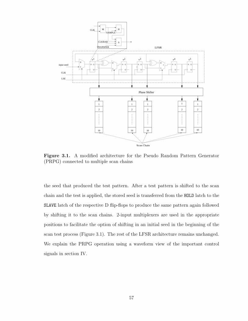
CLK
LSE
M H
S
CLK
CLKBAR
TRANSFER
SAMPLE
1 x x2
0
1
0
1
xxxxx
1
0
1
2
10
1
2
10
1
2
10
1
2
10
1
2
10
input seed
LFSR
Phase Shifter
51 2 3 4
Scan Chain
Q
Q’
D Q
Q’
D Q
Q’
DQ
Q’
D Q
Q’
D
Figure 3.1. A modified architecture for the Pseudo Random Pattern Generator(PRPG) connected to multiple scan chains
the seed that produced the test pattern. After a test pattern is shifted to the scan
chain and the test is applied, the stored seed is transferred from the HOLD latch to the
SLAVE latch of the respective D flip-flops to produce the same pattern again followed
by shifting it to the scan chains. 2-input multiplexers are used in the appropriate
positions to facilitate the option of shifting in an initial seed in the beginning of the
scan test process (Figure 3.1). The rest of the LFSR architecture remains unchanged.
We explain the PRPG operation using a waveform view of the important control
signals in section IV.
57
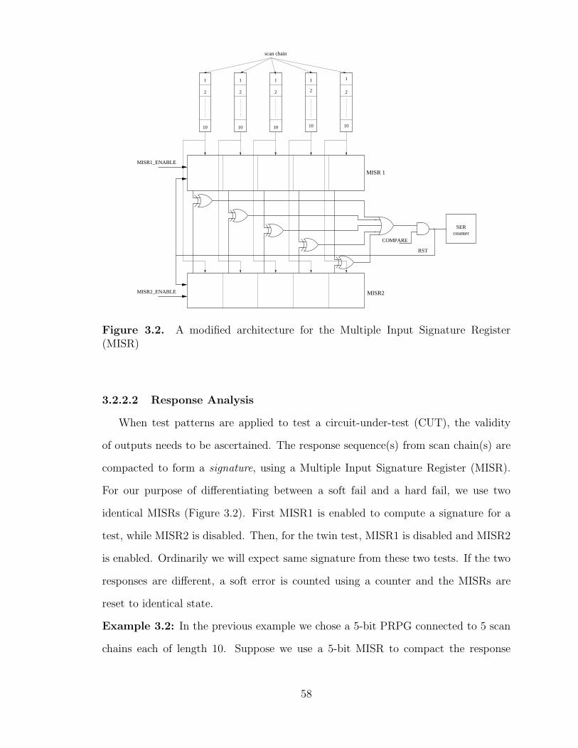
10
SERcounter
COMPARE
RST
MISR 1
MISR2
scan chain
MISR2_ENABLE
MISR1_ENABLE
1
2
10
1
2
10
1
2
10
1
2
10
1
2
Figure 3.2. A modified architecture for the Multiple Input Signature Register(MISR)
3.2.2.2 Response Analysis
When test patterns are applied to test a circuit-under-test (CUT), the validity
of outputs needs to be ascertained. The response sequence(s) from scan chain(s) are
compacted to form a signature, using a Multiple Input Signature Register (MISR).
For our purpose of differentiating between a soft fail and a hard fail, we use two
identical MISRs (Figure 3.2). First MISR1 is enabled to compute a signature for a
test, while MISR2 is disabled. Then, for the twin test, MISR1 is disabled and MISR2
is enabled. Ordinarily we will expect same signature from these two tests. If the two
responses are different, a soft error is counted using a counter and the MISRs are
reset to identical state.
Example 3.2: In the previous example we chose a 5-bit PRPG connected to 5 scan
chains each of length 10. Suppose we use a 5-bit MISR to compact the response
58

obtained from the scan chains to produce a signature. The internal architecture of
a MISR is exactly similar to that of a 5-bit division type LFSR in the sense that a
5-bit MISR will consist of 5 flip-flops and XORs embedded in between the flip-flops
at the positions where the compaction polynomial C(x) (of degree 5 in this case) has
the non-zero co-efficient x terms. �
We compare the signatures for a pattern and its twin in the following test cycle
to detect the presence of a soft fail. In case of detection of a soft fail, a counter is
incremented by 1 to count the SER followed by resetting both the MISRs (Figure 3.2).
The reset is needed to avoid the difference between the current signatures to influence
the future signatures erroneously. If, however, no difference is noticed between the
two signatures, we may infer one of the following two cases:
1. The CUT response is fault-free; or
2. The CUT has a hard fail.
To resolve the second issue, we periodically collect the signature from one of the
MISRs and compare with a golden signature to identify the presence of a hard fail
in the CUT. However, if the soft error count in a test interval is positive, hard fail
cannot be detected for that interval without restarting the test.
It should be worthwhile mentioning here that if a soft error occurs in the LFSR
logic block during loading the initial seed, it may flip one or more bits of the seed
resulting in latching a different seed compared to the intended one. However, this
does no impact on the proposed BIST scheme as only the latched seed will be used
to produce the pseudo-random input patterns to be applied during two consecutive
application of the same test set. On the other hand, if a soft error occurs during
pattern generation phase of the LFSR, it will produce two different sets of pseudo-
random patterns to be applied on the CUT and consequently producing two different
MISR signatures reporting in incrementing the SER count. Similarly, a soft error
59

LSE
SAMPLE
TRANSFER
LFSR normal operation(serially loading the scan chains attached to LFSR)
LFSR normal operation(serially loading the scan chains attached to LFSR)
PATTERN I DUPLICATE PATTERN I
MISR1_ENABLE
MISR2_ENABLE
COMPARE
RST(if a soft error)
is detected
TRANSFER SAMPLEcyclecycle
LFSRsignals
MISRsignals
PATTERN II
Unloading the scan chains to MISR1 Unloading the scan chains to MISR2
cycleTRANSFER
(serially loading the scan chains attached to LFSR)
CLK
CLKBAR
scan−in initial seedto LFSR
MODE CONTROLSCAN TEST SCAN SCANTEST TEST SCAN
DUPLICATEPATTERN II
1 2 3 4 5 76 8 9 10 11 12 13 14 15 16 17 18 19 20 21 22 23 24 25 2726 28 29 30 424140393837363534333231
Figure 3.3. A waveform view of the control signals used in the PRPG and the MISRof the proposed architecture
occurring in one of the two MISRs during test will produce a non-matching signature
thereby detecting a soft error.
3.2.3 Built-In Self-Test Operation
With the above discussion on proposed BIST architecture we now focus on enun-
ciating the operation of the BIST in further detail with the aid of a waveform view
of the important control signals used. To illustrate the idea we continue with the
example constructed with a 5-bit PRPG connected to 5 scan chains each of length
10.
Example 3.3: In Figure 3.3, a snapshot of 42 clock cycles of the BIST operation is
shown. In the initial phase, the LFSR scan enable (LSE) signal is held HIGH for 5
clock cycles to shift in the initial seed to the LFSR. At the LOW phase of the 5th clock
cycle the seed stored in the MASTER latch of the flip-flop blocks get stored in the HOLD
latches with the trigger of the SAMPLE signal.
A MODE CONTROL signal is connected to the scan chains, which remains HIGH for
10 clock cycles during the scan-in operation, followed by a LOW cycle when the test
is applied to the CUT. In the test cycle (say, cycle 16 of Figure 3.3) the TRANSFER
signal becomes HIGH for half-a-cycle to transfer the stored seed from the HOLD latch
60
to the SLAVE latch to generate the duplicate pattern to be applied in the next test
cycle.
In the MISR side, two MISR enable signals associated with the MISRs (MISR1 ENABLE
and MISR2 ENABLE respectively) work in lock step with the MODE CONTROL signal to
collect the response sequences from the scan chains. When both the MISRs obtain
the response for a given pattern and its duplicate, a COMPARE signal is applied in the
next clock cycle (say, cycle 38 in Figure 3.3) which observes a difference if a soft error
occurred. If a soft error occurs, it triggers a RST signal which resets both MISRs. �
3.2.4 Applicability of the Scheme
The pseudo-random test patterns generated by the proposed BIST-based approach
excite a set of nodes in their vulnerable state. If a single event transient (SET) occurs
in any of these nodes by that pattern during the same clock cycle, a single event upset
(SEU) will get recorded provided the path from the output of the SET-affected node
is sensitized to a memory element or a primary output. Since single event transients
are rare events, it may be of practical interest to insert control points and observation
points at appropriate locations [50] to improve the soft error detection rate to reduce
the overall SER test application time. However, improvement in testability also
artificially increases the SER count which has to be scaled appropriately to obtain
the actual SER characterization data. We perform random pattern fault simulations
before and after insertion of control and observation points and count the number
of faults detected in each case. The ratio between these two counts establishes the
scaling factor to obtain the actual SER count from field data. The following example
illustrates the need for inserting control points and observation points in further
detail.
Example 3.4: Let us consider a 32-input AND gate (Figure 3.4(a)). The output z
will be in logic 1 state only when all 32 inputs of the AND gate are assigned logic
61
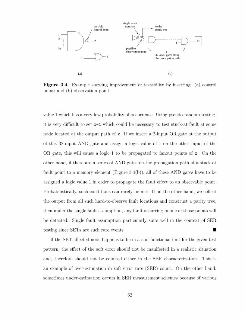
to theparity tree
(b)
FF11
possibleobservation point
32 AND gates alongthe propagation path
transientsingle event
11
(a)
i1i2
i32
control pointpossible
Z
Figure 3.4. Example showing improvement of testability by inserting: (a) controlpoint; and (b) observation point
value 1 which has a very low probability of occurrence. Using pseudo-random testing,
it is very difficult to set z=1 which could be necessary to test stuck-at fault at some
node located at the output path of z. If we insert a 2-input OR gate at the output
of this 32-input AND gate and assign a logic value of 1 on the other input of the
OR gate, this will cause a logic 1 to be propagated to fanout points of z. On the
other hand, if there are a series of AND gates on the propagation path of a stuck-at
fault point to a memory element (Figure 3.4(b)), all of these AND gates have to be
assigned a logic value 1 in order to propagate the fault effect to an observable point.
Probabilistically, such conditions can rarely be met. If on the other hand, we collect
the output from all such hard-to-observe fault locations and construct a parity tree,
then under the single fault assumption, any fault occurring in one of those points will
be detected. Single fault assumption particularly suits well in the context of SER
testing since SETs are such rare events. �
If the SET-affected node happens to be in a non-functional unit for the given test
pattern, the effect of the soft error should not be manifested in a realistic situation
and, therefore should not be counted either in the SER characterization. This is
an example of over-estimation in soft error rate (SER) count. On the other hand,
sometimes under-estimation occurs in SER measurement schemes because of various
62

filtering effects. We observe that any soft error measurement scheme is biased because
detection of soft error is highly pattern dependent. Changing the pattern from one
to another may cause no error, few errors or a large set of errors because a large
set of transient errors may get exposed by a specific pattern, which could have been
masked by another pattern. Therefore, SER estimation provides a raw figure which,
therefore, should be scaled appropriately by evaluating the test set in a simulation
environment. Once this scaling factor is known for a given test set, we may obtain
the accurate SER count from the raw count that was obtained from the proposed
BIST technique.
Finally, pseudo-random testing typically offers very little diagnostic resolution
because a sequence of responses over a period of time gets compressed in a single
signature through MISR. However, in the proposed BIST method we perform cycle-
by-cycle comparison between two signatures obtained by applying the same test pat-
tern twice in a row. The signatures would mismatch only in presence of a transient
fault. Since single event transients (SET) are rare events, the probability of occur-
rence of more than one SET on any given test cycle is fairly minuscule. Also, the
aliasing probability of two different SET locations in a CUT with identical signature
will reduce exponentially with the length of the MISR [126]. If we maintain a map
between a transient failure location and its signature, the diagnostic resolution of the
proposed BIST scheme can be significantly improved. The diagnostic result can then
be used for selective radiation hardening of a circuit in subsequent design iterations.
3.2.5 DFT Extension to Facilitate Application of Targeted Patterns
In Chapter 2, we proposed pattern selection techniques to identify test cubes that
specifically target a set of soft-error susceptible nodes at their respective vulnerable
state. Given the fact that soft-errors are rare events, the broad idea was to excite
as many soft-error susceptible sites as possible on every single test cycle so as to
63

To scan chainPhase Shifter
y y y y y1 2 3 4 5 H= 0 1 0 0 0
0 0 0 0
1 0 1 0 1
1
0 0 1 0 0
0 0 0 1 0
(a) (b)
Figure 3.5. (a) LFSR and phase shifter. (b) State transition matrix of the LFSR.
maximize the cumulative probability of detection of a single event transient on any
given test cycle.
On the other hand, the DFT architecture proposed in this chapter uses a pseudo-
random pattern generator (PRPG) to generate and apply pseudo-random patterns to
a given circuit-under-test (CUT). The pseudo-random patterns are generated based
on the feedback polynomial used to realize the basic Linear Feedback Shift Register
(LFSR) for the PRPG. However, given the scan-chain architecture for the CUT, the
PRPG feedback polynomial and phase shifter (if any), it is possible to symbolically
simulate the operation of the PRPG and the phase shifter to determine a system of
linear equations for a given test cube. The resulting system of linear equations have
the form A~y = ~z, where A is a matrix that can be derived from the PRPG feedback
polynomial and the phase shifter, ~z is a column vector corresponding to the specified
bits in the test cube, and the solution for the vector ~y is the seed that will be applied
from the tester to the PRPG. The following example, originally presented in [124],
illustrates the seed computation process.
Example 3.5: Let us consider the external-XOR LFSR with feedback polynomial:
p(x) = x5 + x3 + x + 1, and a one-stage phase shifter as shown in Figure 3.5. The
state of the LFSR can be represented using a vector ~S = (s1, s2, . . . , sN)t, where N is
the size of the LFSR and s1(sN) corresponds to the leftmost(rightmost) stage. The
64

1 0 1 0 0
1 1 1 0 1
0 1 1 1 1
y
y
y
y
y
1
2
3
4
5
= 0
1
1
1 0 0 1 0 1
0 1 0 0 1 1
0 0 1 1 0 0
(b)
PivotsFree
Variables
y1
y2
y3
= y4
1
0
1
+ y5
0
1
0
+
1
1
0
(c)
(a)
Figure 3.6. Example to illustrate the solution for a system of linear equations. (a)System of linear equations. (b) Gauss-Jordan elimination. (c) Solution space.
jth state of the LFSR is derived recursively as ~Sj = H~Sj−1, with j = 1, 2, . . ., where
H is the state transition matrix for the LFSR (shown in Figure 3.5(b)).
The jth output of the one-stage phase shifter shown in Figure 3.5 can be repre-
sented as Oj = ~P t~Sj = ~P tHj~S0, where j = 1, 2, . . .. The vector ~P represents the
operation of the phase shifter. If stage j of the LFSR is connected to the XOR
gate, the jth row in ~P is said to be “1”. For the phase shifter in Figure 3.5,
we have ~P = (10100)t. For example, the second output of the phase shifter is
O1 = ~P tH~S0 = (11101)~S0 = y1 + y2 + y3 + y5.
For the test cube 101xxxxx (the leftmost bit “1” is loaded into the first scan cell
that is next to the scan-out pin), we can obtain a system of linear equations, as
shown in Figure 3.6(a). Gauss-Jordan elimination [24] can be used to transform a
set of columns in A into an identity matrix (these columns are referred to as pivots),
while the remaining columns are free variables, as shown in Figure 3.6(b). The set of
65
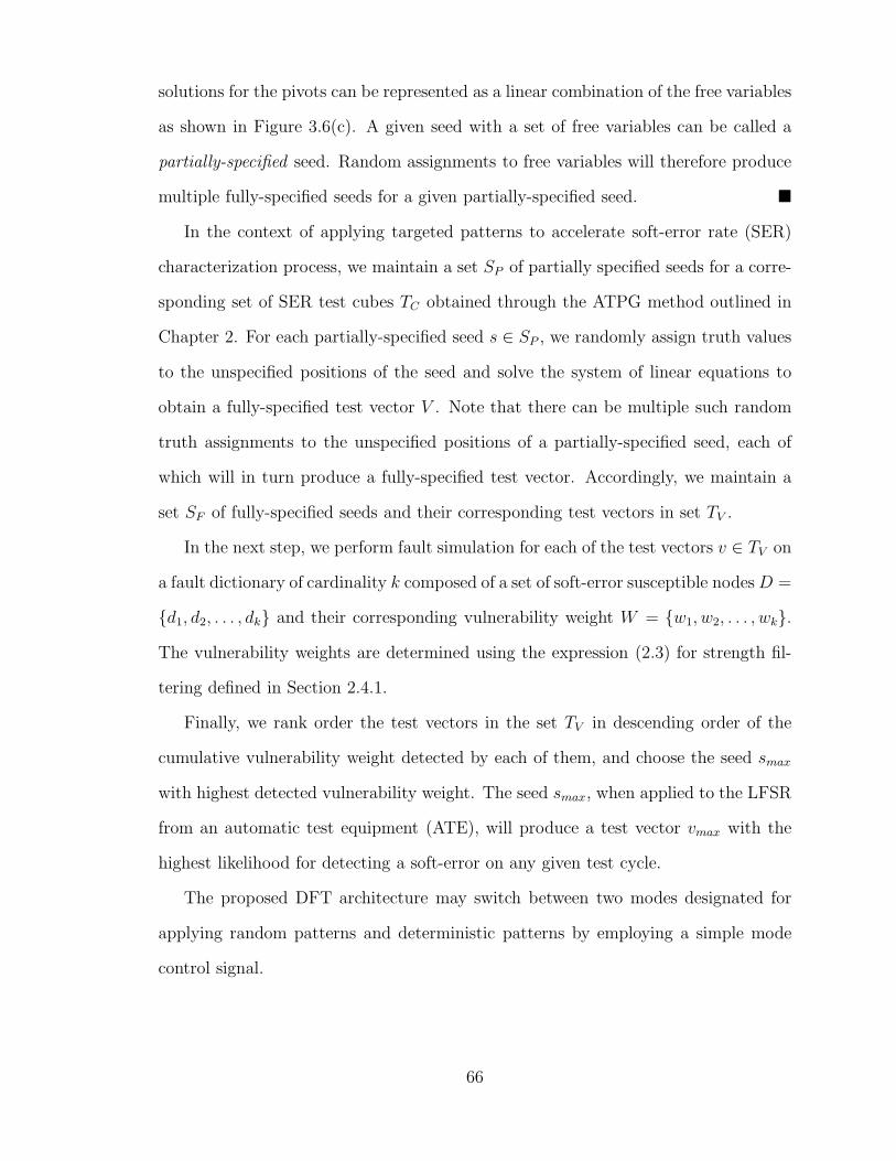
solutions for the pivots can be represented as a linear combination of the free variables
as shown in Figure 3.6(c). A given seed with a set of free variables can be called a
partially-specified seed. Random assignments to free variables will therefore produce
multiple fully-specified seeds for a given partially-specified seed. �
In the context of applying targeted patterns to accelerate soft-error rate (SER)
characterization process, we maintain a set SP of partially specified seeds for a corre-
sponding set of SER test cubes TC obtained through the ATPG method outlined in
Chapter 2. For each partially-specified seed s ∈ SP , we randomly assign truth values
to the unspecified positions of the seed and solve the system of linear equations to
obtain a fully-specified test vector V . Note that there can be multiple such random
truth assignments to the unspecified positions of a partially-specified seed, each of
which will in turn produce a fully-specified test vector. Accordingly, we maintain a
set SF of fully-specified seeds and their corresponding test vectors in set TV .
In the next step, we perform fault simulation for each of the test vectors v ∈ TV on
a fault dictionary of cardinality k composed of a set of soft-error susceptible nodesD =
{d1, d2, . . . , dk} and their corresponding vulnerability weight W = {w1, w2, . . . , wk}.
The vulnerability weights are determined using the expression (2.3) for strength fil-
tering defined in Section 2.4.1.
Finally, we rank order the test vectors in the set TV in descending order of the
cumulative vulnerability weight detected by each of them, and choose the seed smax
with highest detected vulnerability weight. The seed smax, when applied to the LFSR
from an automatic test equipment (ATE), will produce a test vector vmax with the
highest likelihood for detecting a soft-error on any given test cycle.
The proposed DFT architecture may switch between two modes designated for
applying random patterns and deterministic patterns by employing a simple mode
control signal.
66
M M
ControllerCentral BIST
M1 2 n
Figure 3.7. Block diagram view of a distributed BIST process
3.2.6 Architecture for Testerless Test Scheduling and Test Methodology
Keeping in mind that soft error rate (SER) is expensive to measure because of the
time scales associated with soft error, we propose a BIST-based distributed SER mea-
surement scheme which does not require any external tester, thereby greatly reducing
the SER test cost. As mentioned in Section 3.2.2, the proposed BIST architecture
operates in non-concurrent on-line mode. When a machine Mi (Figure 3.7) remains
idle for some pre-determined constant time, a centralized BIST controller activates
the BIST operation by sending the initial seed to the machine. When an interrupt
occurs at the machine Mi, the proposed BIST controller collects the SER count data
from the counter and sets the machine Mi back to its normal operation mode. The
need for a tester can be completely eliminated in this case by making use of a custom
test board where the individual devices are plugged in to the appropriate slots in the
board and parallel testing of multiple devices can be conducted by using a central
test controller which sends the initial seed to individual device-under-test (DUT).
When a soft error gets detected in a DUT, the test controller gets informed about
67
the occurrence of the soft error where it maintains a centralized SER count followed
by resetting the MISRs in the respective DUT and restart the test process.
3.3 Application II – Test for Circuit Marginality Faults
3.3.1 Background and Related Work
As mentioned earlier, localized power dissipation within the elements of an in-
tegrated circuit is on rise and can cause chip temperature gradients and variations
which strongly affect the performance of the circuit [33]. Since the failure rate of mi-
croelectronic devices doubles for approximately every 10◦C increase in temperature,
hot-spots due to excessive local power dissipation have become a major long term reli-
ability concern in ultra deep sub-micron regime. In addition, the resolution of mixed
analog-digital ICs is reaching levels where parasitic thermal and electrical interactions
limit accuracy. Examples of thermally induced performance failures include input off-
set voltage and offset voltage drift in differential amplifiers, reference voltage shifts
in regulators and data converters etc. To optimize both long-term reliability and
performance, it has become essential to perform both thermal and electro-thermal
simulations prior to chip fabrication [69]. Several computer aided design (CAD) tools
have been proposed in literature focusing on thermal and electro-thermal simulation
in the device level and the small scale integrated (SSI) level [29,33,69]. The attempt
at providing the electro-thermal simulation capability at the VLSI level was intro-
duced in ILLIADS-T [22] and was further improved in iTAS [21]. Thermal modeling
at the processor-architecture level was studied by Skadron et al [108]. Even though
a notable attention has been given on thermal modeling and simulation aspects of
an integrated circuit, there is hardly any study on testing circuit marginality related
failures caused by temperature effects. Particularly, we did not come across any re-
search which proposed a BIST-based methodology to test transient failures caused
by localized temperature gradients. One primary objective in such BIST-based test
68

methodology would be to select a pre-defined set of pseudo-random test patterns
to cause extremely high localized switching activity in the target functional unit to
develop thermal hotspot(s). In a typical LFSR-based BIST architecture, selection
of the initial seed will have a major influence in generating an appropriate test set.
However, identification of the appropriate set of tests is out of the scope of this paper.
Testing of circuit marginality related failures for product chips would also require
BIST circuits and test methodology to reduce test cost and time. All the motivations
behind using BIST for test economics, test complexity and time reductions as reported
by Agrawal et al. [5] also apply to the BIST-based circuit marginality testing.
In this context, we now suggest using the proposed linear feedback shift regis-
ter (LFSR) and multiple-input signature register (MISR)-based BIST architecture
(as described in Section 3.2.2) for testing the performance degradation issues due to
temperature effects. Although major architectural elements in BIST technique for
circuit marginality testing is similar to the modified LFSR/MISR-based BIST archi-
tecture presented in Section 3.2.2, we will observe a few minor differences in the BIST
structure and operation scheme in the following two subsections.
3.3.2 The Proposed Architecture
We follow a non-concurrent on-line BIST-based two-pronged approach [102] to
detect thermal hot-spot related transient failures:
1. Apply a specific set of pseudo-random patterns to the functional unit under test
at a nominal frequency and collect the signature in a MISR, which constitutes
the reference signature for the remaining test process;
2. Reapply the test set in the target functional unit while shmooing the frequency
following the principle of Fmax testing [72] and compare the MISR signature
with the reference signature computed in step 1.
69
Frequency
Step
P
P
P
PP
PF
F
FFF
Maximum safeoperating frequency
Figure 3.8. Plot showing the principle of Fmax testing based on frequency shmoo
The last noted operating frequency is identified as the safe maximum operating
frequency for the given functional unit. As the frequency is increased the failure point
is affected by the cumulative power dissipation. This results in hysteresis as shown
in Figure 3.8.
The basic BIST architecture is quite similar to the one described in Section 3.2.2
and consists of three hardware blocks: i〉 a pattern generator, ii〉 a response ana-
lyzer, and iii〉 a test controller. We use a linear feedback shift register (LFSR)-based
pseudorandom pattern generator (PRPG) to feed random patterns to multiple scan
chains. A multiple input signature register (MISR) is used to perform a compaction
operation [5] on the outputs of the scan chains to produce a signature.
In the following two subsections we describe the modified PRPG architecture and
the MISR-based signature analysis scheme to enable detection of transient failures
caused by thermal hot-spots generated because of high localized switching activity in
a functional unit.
3.3.2.1 Pattern Generation
As the frequency is gradually raised a circuit will eventually fail. This failure may
or may not be caused by circuit marginality problems. Circuit marginality related
70

problems arise when a part fails within its rated frequency while it works at frequencies
lower and even possibly higher. One reason for circuit marginality failure is due to
temperature conditions, while the others are related to power supply noise and noise
on the signal lines. When the patterns are applied repeatedly thermal hot-spots or
local power supply drop may occur and that is what we wish to capture with our
pseudo-random testing method.
As mentioned in Section 3.2.2.1, Linear Feedback Shift Registers (LFSRs) are
widely deployed as pseudorandom pattern generators (PRPG) in a BIST environment.
An n bit LFSR realizes a primitive polynomial p(x) of degree n, which produces 2n−1
distinct non-zero bit strings of length n starting with an initial seed [7].
The detailed description of the basic PRPG architecture (Figure 3.1) and its pro-
posed modification to enable detection of transient errors appears in Section 3.2.2.1.
3.3.2.2 Response Analysis
When test patterns are applied to test a functional unit, the validity of outputs
needs to be ascertained. The response sequence(s) from scan chain(s) are compacted
to form a signature, using a Multiple Input Signature Register (MISR). For our pur-
pose of detecting a thermal hotspot-induced transient failure, we use two identical
MISRs (Figure 3.9). First MISR1 is enabled to compute the reference signature for
a given set of pseudo-random test patterns at a nominal operating frequency. Sub-
sequently when the same set of patterns is applied for the next time onward, the
reference signature in MISR1 is left intact while MISR2 is used to collect the signa-
ture for the given test set at different frequency stages. This is slightly different from
the strategy we employed for response analysis in the context of SER measurement.
Ordinarily we will expect same signature from these two identical tests. If the two
responses are different, a transient failure is detected. Otherwise, the test process
continues after resetting MISR2.
71
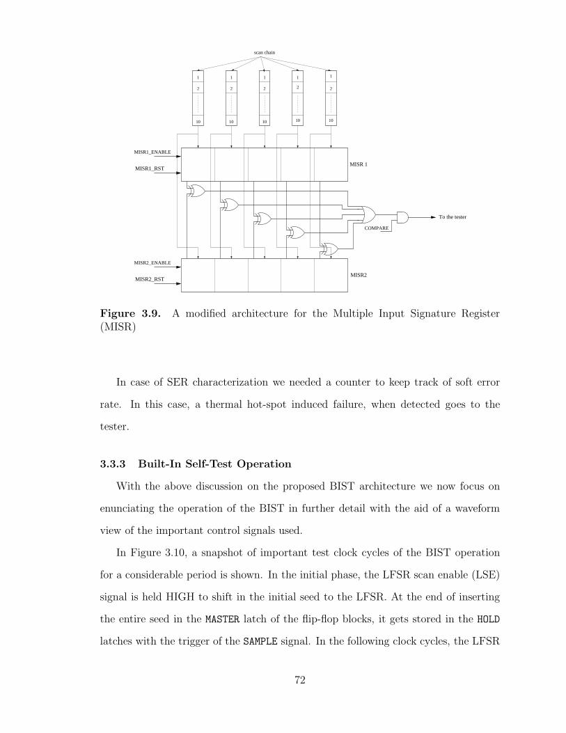
10
COMPARE
scan chain
MISR1_ENABLE
MISR1_RSTMISR 1
MISR2
To the tester
MISR2_RST
MISR2_ENABLE
1
2
10
1
2
10
1
2
10
1
2
10
1
2
Figure 3.9. A modified architecture for the Multiple Input Signature Register(MISR)
In case of SER characterization we needed a counter to keep track of soft error
rate. In this case, a thermal hot-spot induced failure, when detected goes to the
tester.
3.3.3 Built-In Self-Test Operation
With the above discussion on the proposed BIST architecture we now focus on
enunciating the operation of the BIST in further detail with the aid of a waveform
view of the important control signals used.
In Figure 3.10, a snapshot of important test clock cycles of the BIST operation
for a considerable period is shown. In the initial phase, the LFSR scan enable (LSE)
signal is held HIGH to shift in the initial seed to the LFSR. At the end of inserting
the entire seed in the MASTER latch of the flip-flop blocks, it gets stored in the HOLD
latches with the trigger of the SAMPLE signal. In the following clock cycles, the LFSR
72

LSE
SAMPLE
TRANSFER
MISR1_ENABLE
MISR2_ENABLE
COMPARE
LFSRsignals
MISRsignals
CLK
CLKBAR
1 2 3 4 5 76 8 9 10
cycle cycleTRANSFER TRANSFER
cycleTRANSFER
cycleTRANSFER
scan−in initial seedto LFSR
A specific workload applied toa target functional unit
Unloading the scan chainsto MISR1
Same workload applied againat a higher frequency
Same workload applied onceagain at a even higher frequency
Same workload applied at afurther higher frequency
Unloading the scan chainsto MISR2
Unloading the scan chainsto MISR2
MISR2_RST
Figure 3.10. A waveform view of the control signals used in the PRPG and theMISR of the proposed architecture
continues generating pseudo-random patterns starting with the initial seed and the
entire set of test patterns passes through the scan chain(s) causing high switching
activity in the target functional unit. After the entire test set is applied in the target
functional unit, the following two operations take place:
1. The TRANSFER signal becomes HIGH for half-a-cycle to transfer the stored seed
from the HOLD latch to the SLAVE latch to generate the same test set to be
applied again to the functional unit under test; and
2. The MISR1 ENABLE signal is asserted HIGH to start computing the reference
signature in MISR1 while the duplicate test set is applied in the target functional
unit.
After the initial reference signature gets collected in MISR1, all subsequent signa-
tures are collected in MISR2 by asserting the MISR2 ENABLE signal HIGH during the
appropriate test cycles.
Every time the MISR2 finishes computing the signature for the given test set at
a specific frequency, a COMPARE signal is applied in the next clock cycle (shown in
Figure 3.10) to compare the signature of MISR2 with the reference signature in MISR1,
73
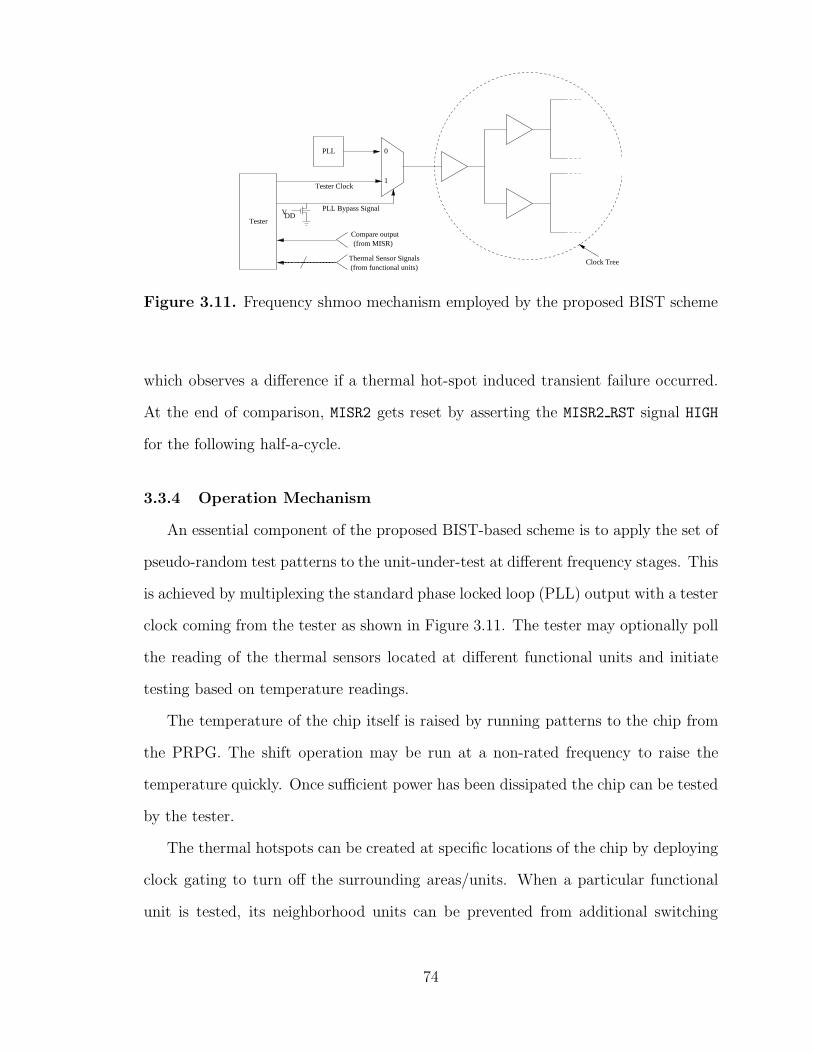
PLL
Tester Clock
Clock Tree(from functional units)Thermal Sensor Signals
PLL Bypass SignalDDV
1
0
Tester
Compare output(from MISR)
����������������������
����������������������
Figure 3.11. Frequency shmoo mechanism employed by the proposed BIST scheme
which observes a difference if a thermal hot-spot induced transient failure occurred.
At the end of comparison, MISR2 gets reset by asserting the MISR2 RST signal HIGH
for the following half-a-cycle.
3.3.4 Operation Mechanism
An essential component of the proposed BIST-based scheme is to apply the set of
pseudo-random test patterns to the unit-under-test at different frequency stages. This
is achieved by multiplexing the standard phase locked loop (PLL) output with a tester
clock coming from the tester as shown in Figure 3.11. The tester may optionally poll
the reading of the thermal sensors located at different functional units and initiate
testing based on temperature readings.
The temperature of the chip itself is raised by running patterns to the chip from
the PRPG. The shift operation may be run at a non-rated frequency to raise the
temperature quickly. Once sufficient power has been dissipated the chip can be tested
by the tester.
The thermal hotspots can be created at specific locations of the chip by deploying
clock gating to turn off the surrounding areas/units. When a particular functional
unit is tested, its neighborhood units can be prevented from additional switching
74
activity by clock gating. Also the proposed BIST-based scheme can be used to dis-
tinguish between a hotspot-induced failure and a simple delay failure by first testing
it at a target frequency, and if it passes the test then ramping up the tester clock
frequency above the rated frequency for a certain period followed by reapplying the
tests at the rated frequency. Should the circuit fail following the frequency ramp, tem-
perature induced failure is detected as the only parameter that would have changed
in the interim period is the temperature in the unit under test.
3.3.5 Characterization of Impact on Neighborhood
In this sub-section, we propose a design-for-testability (DFT) scheme which will
facilitate the BIST methodology to target a particular functional unit to stimulate
high switching activity for a considerable duration and to observe its impact on the
neighborhood functional units. This new DFT scheme can also be used to develop
thermal hot-spots in the neighborhood units of a specific functional unit while keeping
it in a nominal temperature and observe the impact of “hot” neighborhood on it. The
following example explains the DFT scheme in further detail.
Example 3.6: In Figure 3.12, we show a chip consisting of 9 functional units. Scan-
bypass circuitry as shown in this figure can be used to limit activity to target func-
tional units. The fan-in count of the MUX depends on the number of functional
units the scan chain passes through because each of these boundaries will tap out
one bypass path to the MISR. The control signals connected to the AND gates to-
gether with the corresponding MUX select signal facilitates the selection of one or
more functional units to be exercised with high switching activity for a fixed dura-
tion to characterize the impact of neighborhood in the context of testing thermal
hotspot-induced transient failures. �
75

scan chains
control
scancells
signal
0 1
0 1
LFSR
MISR
FU1
FU2
FU3
FU4
FU5
FU6
FU7
FU8
FU9
MISR
Figure 3.12. Scan path modifications to test thermal hotspot-induced transientfailures
3.4 Overhead of the Scheme
We have analyzed the hardware overhead of the proposed BIST scheme. It adds
one additional latch per flip-flop in the LFSR side with a space complexity of O(k),
where k is the number of scan chains connected to the LFSR. On the MISR side,
four additional components are added to facilitate the proposed architecture: i〉 an
identical MISR to store the response of the duplicate pattern, ii〉 k XOR gates, where
k is the length of the MISR (or equivalently, the number of scan chains supported
by the design), iii〉 an SER counter (when used for SER characterization), and (d) a
minimum size AND gate with the COMPARE input. Synthesizing RTL description of
the original LFSR and MISR based BIST and then with the proposed modifications,
we quantified percentage area increase in the BIST for various LFSR and MISR sizes
76

Original Design [42] ASIC1 ASIC2 ASIC3 ASIC4
Raw gate count 180K 356K 550K 748KNumber of scan chains 80 128 128 120LFSR bit-length 31 31 31 31MISR bit-length 80 80 80 31BIST chip area overhead (%) 1.3 1.3 1.0 0.8
With Proposed BIST ASIC1 ASIC2 ASIC3 ASIC4
BIST area increase (%) 140 140 140 130BIST chip area overhead (%) 1.8 1.8 1.4 1.1Total chip area overhead (%) 0.5 0.5 0.4 0.3
Table 3.1. BIST Area Overhead by the Proposed Design as Observed in VariousIndustrial Designs
with 8-bit SER counter. The proposed architecture is highly scalable to the input
size of the circuit-under-test.
Table 3.1 illustrates the area overhead of proposed BIST architecture enhance-
ments for SER characterization on four large industry designs from [42]. The original
logic BIST design with LFSR and MISR consume up to 1.3% of the total chip area.
Although the proposed scheme increases BIST area by as high as 140%, area overhead
on total chip area is still only 1.1 to 1.8%. Therefore, total chip area increase due to
the proposed BIST scheme is insignificant for large designs.
Another obvious overhead of the proposed BIST scheme is the increase in test
time. Due to low frequency of transient errors, accurate experimental characterization
of SER and other circuit marginality related transient errors can take significantly
long time even in accelerated environments such as placing the device in a radiation
chamber in case of SER measurement. However, the long test time is an inherent
problem in any transient error testing and conventional test methods with a tester
and device-under-test would only increase the associated test cost. The proposed
BIST scheme would enable parallel testing for test time reduction, simple tester for
77

low cost, and may even facilitate a testerless test methodology for soft error rate
measurement as proposed in Section 3.2.5.
3.5 Cost-benefit Analysis of the Proposed Approach
Burn-in test, which is a part of the manufacturing test flow, is often run for many
hours and even up to a week. As SER characterization test is not done on the entire
population of chips, but rather on a sample, it is reasonable to assume that such
characterization test can be done over multiple weeks or even months. Keeping in
mind that soft-error rate (SER) is expensive to measure because of the time scales
associated with soft-error. The proposed BIST-based scheme, when applied in a
distributed environment with a central BIST controller, as presented in Section 3.2.6,
will greatly reduce the SER characterization cost.
The benefit of the self-test approach can be seen as if a sample of 1000 chips
is tested for 1-2 months with 1000X acceleration in a radiation chamber. With the
proposed BIST-based approach, we can easily characterize SER in a cost-effective
and timely manner.
It has been reported that temperature of a chip can rise as fast as 25 ◦C/sec under
functional conditions [68]. Under non-functional conditions as suggested in Section
3.3.1, we estimate that a chip can easily be heated up in 10 seconds or less. Thus, for
thermal testing the proposed approach can accomplish measurements at two different
temperatures within a reasonable time frame of 10-15 seconds making the solution
practical.
3.6 Conclusions
Circuit marginality related transient failures, such as thermal hot-spot induced
delay failures or single event upsets (SEU) caused by high energy particles, are on
the rise. Also, the soft error rate (SER), represented as number of failures encoun-
78

tered per billion hours of device operation, is expensive to measure. In this chapter,
we proposed a non-concurrent on-line built-in self-test (BIST)-based approach which
accurately distinguishes a transient failure from a permanent failure, counts total
number of soft errors in the context of SER characterization, and greatly reduces the
test application time and test cost by dissociating a tester from such measurements.
The proposed BIST based SER measurement scheme can be accelerated further by
improved controllability and observability, while unlike traditional BIST schemes, a
test-by-test failure detection capability enables higher diagnostic resolution for single
event based transient errors. With the proposed BIST architecture, we were also able
to study the thermal hot-spot induced delay failures and the effect of temperature on
specific functional units. We used the principle of Fmax testing based on frequency
shmoo to determine maximum safe operating frequency of individual functional units
of a chip. A design-for-testability (DFT) scheme is proposed to characterize the im-
pact of a “hot” unit on its neighborhood and the influence of a “hot” neighborhood
on relatively “cold” units in the opposite way. In the context of SER measurement,
a distributed network controller is proposed to facilitate the measurement over a net-
work of machines that obviates the need for a tester. Thus the proposed architecture
extends the capability of BIST to test a certain class of circuit marginality related
transient failures with a very low hardware overhead.
79

CHAPTER 4
STUDY OF MULTIPLE AGGRESSOR CROSSTALK
NOISE IN PRESENCE OF SELF-LOADING EFFECTS
4.1 Introduction
Increase in circuit density and switching speed has led to an increasing number
of signal integrity related failures in VLSI circuits [128]. Capacitive crosstalk is one
of the major sources of such failures. Crosstalk fault results from parasitic coupling
between adjacent signal nets and is more common in nets that have weaker drivers
relative to their adjacent peers. Current trends in integrated circuit design indicate
that interconnect sidewall coupling capacitances can be significant, thus increasing
the parasitic coupling.
Crosstalk effects can be categorized into two types: i〉 crosstalk induced pulses
and ii〉 crosstalk induced delay. The first manifests as a pulse on a line, called
the victim, which should remain in a static state when one or more capacitively
coupled neighboring lines, called the aggressors, have a transition. Depending on
their amplitude and width, these pulses may cause logic malfunction [106]. The
second effect, crosstalk delay, is observed when both the aggressor(s) and victim nets
have simultaneous or near-simultaneous transitions. If both lines undergo transition in
the same direction, their transition times are reduced causing a reduction in effective
delay. We refer to this phenomenon as crosstalk speedup. If, on the other hand, the
aggressor(s) and victim switch in opposite direction, then there will be an increase
in delay, which is called crosstalk slowdown. These unexpected changes in signal
propagation delays may also cause faulty behaviors and adversely affect the circuit
performance [20].
80
Signal integrity problems have been aggravated by variations in the fabrication
process [128] or usage of dynamic logic families [59]. With scaling, the problem gets
exacerbated due to reduced noise threshold and increased noise arising out of sharper
signal transitions.
Gate leakage current due to reduced oxide thickness has emerged as a major
concern in sub-65nm technology nodes. In fact, gate leakage is expected to increase at
least by a factor of 10X for each of the future generations [49]. Recent studies [82,104]
show that different sources of leakage can affect each other by interacting through
resultant intermediate node voltages, known as the loading effect. The effect of loading
is expected to grow more prominent with further scaling of device dimensions. Recent
introduction of high-K gate dielectric material provides a one time relief from gate
oxide leakage, which increases again as dielectric thickness is scaled.
Since loading effect perturbs internal node voltages, noise margins are reduced
further. We infer that combination of these two noises will likely worsen with scaling
as load voltage erodes noise margin further while noise level increases due to sharper
signal transitions. Therefore, gate leakage induced loading should be considered dur-
ing signal integrity analysis for nanometer CMOS designs. To our best knowledge,
this is the first such study which considers these two noise effects together. Combi-
nation of these two noises will likely worsen with scaling as load voltage erodes noise
margin further while noise level increases due to sharper signal transitions.
If it were not for stringent area and performance requirements, signal integrity
problems observed during validation could be eliminated by resizing drivers, re-
routing signals, shielding interconnect lines with power distribution lines and other
such redesign techniques. However, redesign may be very expensive in terms of design
effort and its effectiveness may be offset by process variation. Thus, these problems
need to be tested during manufacturing [19].
81

Both loading effect and crosstalk noise are pattern dependent. In this thesis, we
report the impact of load voltage on capacitive crosstalk in the following two-pronged
way:
• We first perform a dynamic simulation-based study [103] to establish the in-
fluence of gate leakage-induced loading as an aggravating factor for crosstalk
related signal integrity problem.
• Next, we present an automatic test pattern generation (ATPG) solution which
aims at maximizing the combined noise effect due to capacitive crosstalk and
gate leakage loading, followed by propagating the fault effect to an observation
point.
Crosstalk-induced faults are observed more frequently for long nets. A long net
may have multiple fanouts and may be routed through multiple levels of interconnect
metals. Thus, a typical long net is capacitively coupled with multiple aggressors. Due
to sharing of logic, it may not be possible to excite all aggressors while simultaneously
sensitizing a victim net. Moreover, even if all the aggressor nets for a given victim
are excited, it may not be possible to do so in close temporal proximity due to gate
delays. From an automatic test pattern generation (ATPG) point of view, the next
best solution is to switch a set of aggressors in close temporal proximity so as to
maximize the switching of the total coupling capacitance [36]. In this thesis, we
combine this objective together with setting the fanout gates of the given victim in
such a state that it contributes maximal gate leakage loading noise to the victim.
4.2 Related Work
With reduced noise margin and increased noise susceptibility, signal integrity anal-
ysis becomes a metric of comparable importance to area, timing and power for nano-
82
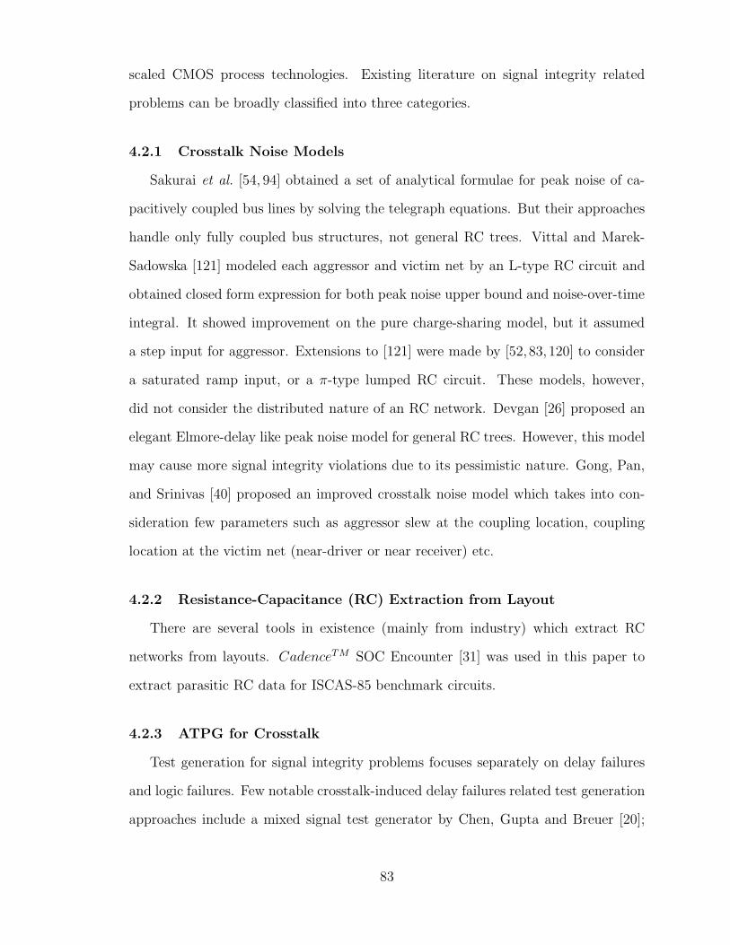
scaled CMOS process technologies. Existing literature on signal integrity related
problems can be broadly classified into three categories.
4.2.1 Crosstalk Noise Models
Sakurai et al. [54, 94] obtained a set of analytical formulae for peak noise of ca-
pacitively coupled bus lines by solving the telegraph equations. But their approaches
handle only fully coupled bus structures, not general RC trees. Vittal and Marek-
Sadowska [121] modeled each aggressor and victim net by an L-type RC circuit and
obtained closed form expression for both peak noise upper bound and noise-over-time
integral. It showed improvement on the pure charge-sharing model, but it assumed
a step input for aggressor. Extensions to [121] were made by [52, 83, 120] to consider
a saturated ramp input, or a π-type lumped RC circuit. These models, however,
did not consider the distributed nature of an RC network. Devgan [26] proposed an
elegant Elmore-delay like peak noise model for general RC trees. However, this model
may cause more signal integrity violations due to its pessimistic nature. Gong, Pan,
and Srinivas [40] proposed an improved crosstalk noise model which takes into con-
sideration few parameters such as aggressor slew at the coupling location, coupling
location at the victim net (near-driver or near receiver) etc.
4.2.2 Resistance-Capacitance (RC) Extraction from Layout
There are several tools in existence (mainly from industry) which extract RC
networks from layouts. CadenceTM SOC Encounter [31] was used in this paper to
extract parasitic RC data for ISCAS-85 benchmark circuits.
4.2.3 ATPG for Crosstalk
Test generation for signal integrity problems focuses separately on delay failures
and logic failures. Few notable crosstalk-induced delay failures related test generation
approaches include a mixed signal test generator by Chen, Gupta and Breuer [20];
83
a GA-based test generator by Krstic et al. [61]; and a multiple aggressor crosstalk-
induced delay problem studied by Paul and Roy [86]. Ganeshpure and Kundu recently
proposed a heuristic ATPG solution for multiple aggressor crosstalk delay failures con-
sidering zero delay [34] and unit delay models [35,36]. These solutions are based on a
heuristic combination of Integer Linear Programming (ILP) and stuck-at-fault ATPG.
In case of crosstalk-induced logic failures, Chen, Gupta and Breuer [19] presented a
crosstalk ATPG solution for single aggressor-single victim scenario. Bai, Dey, and
Krstic [6] proposed a heuristic solution for multiple-aggressor crosstalk ATPG prob-
lem. The ATPG techniques for crosstalk-induced logic failures approaches to find a
pair of test vectors that create the condition for logic violation in a given victim net
by appropriately switching the aggressors, followed by finding a sensitized path from
the logic violation point to an observable output.
On the other hand, in this thesis, we perform 〈i〉 pattern-based dynamic sim-
ulation, and 〈ii〉 a maximization ATPG solution to evaluate and test the effect of
combined voltage noise produced at a victim net because of crosstalk and gate leak-
age loading. We devise an efficient dynamic simulator that reduces the sources of
pessimism involved in static signal integrity analysis. While the dynamic simulator
implicitly considers the Boolean dependencies, we incorporate a timing wheel simu-
lator, first proposed by Ulrich [118], to account for the timing filtering aspect. The
proposed ATPG solution also considers unit delay model to reduce pessimism.
4.3 Signal Delay Model
Signals experience two types of delays. The time interval between an input change
(cause) and the output change (effect) of a gate is called the inertial delay or switching
delay. The time interval between the generation of a signal transition at a gate output
(source) and its arrival at the input of a fanout gate (destination) is known as the
interconnect delay or transport delay [16]. A signal transition at the output of a gate
84
Da
Db
q
p
DD
ac
bccb
a
Figure 4.1. Inertial and transport delay for a 2-input gate
would have to travel through fanout branches of varying lengths before arriving at
the inputs of destination gates. Thus propagation delays are usually specified for
each gate-output and gate-input pair. Rise and fall delays are often considered the
same. It is convenient to specify the transport delay as input delays, separately for
each gate input.
Figure 4.1 (adopted from [16]) shows the complete set of delays specified for a
two-input gate with inputs a and b, and output c. The signal for a is generated at p
and that for b, at q. Four delays for this gate are:
1. Input delay Da is the transport delay for the interconnect p→ a.
2. Input delay Db is the transport delay for the interconnect p→ b.
3. Output delay Dac is the switching delay for an output change caused by a change
at a.
4. Output delay Dbc is the switching delay for an output change caused by a change
at b.
The inertial delay of a gate is considered to be proportional to the total load ca-
pacitance switched by the gate. The static capacitance to ground is obtained from
85

7i
i2
6
i31
34
ig
ig
5
6
p201
0
1
0
p111
0
1
1
i
i1/1
0/1
0/1
1/1
1/1
G1
G2
G
G z1
z2
13C
C
ic
ci
G
1/1
3
4
VN0/0G
Figure 4.2. Illustration of signal integrity problem due to combined effect of capac-itive crosstalk and loading on ISCAS-85 benchmark c17
parasitic RC file (in SPEF format) extracted using SoC EncounterTM [31]. Simi-
larly, the transport delay of an interconnect was modeled as proportional to coupling
capacitance between neighbors, also obtained from the parasitic RC file.
4.4 Impact of Loading Effect on Signal Integrity Analysis
Before going into the detail of the models used for loading effect and capacitive
crosstalk-induced voltage noise estimation and their collective behavior, let us first
establish the problem with the aid of an example as described below.
Example 4.1: Let us choose the smallest ISCAS-85 benchmark c17 which involves
six 2-input NAND gates (Figure 4.2). The circuit has 5 primary inputs {i1,i2,i3,i6,i7}
and 2 primary outputs {z1,z2}. We first apply an input pattern p1={1,1,1,0,1} and
perform logic simulation. The output of gate G3 is in logic state 0 and both its fanout
gates G5 and G6 are in logic state 1. Therefore, gate leakage current (ig) flows from
these two fanout gates (G5 and G6) toward the output net of G3 and causes a loading
voltage noise (say, VL).
86

Now, let us apply a second input pattern p2={0,1,1,0,0}. Logic simulation is
performed and the new logic state at the output of each gate is shown in the figure.
The output of gate G3 remains at logic state 0. We notice that the output net of G3
is capacitively coupled with the output net of gate G1 and G4 (coupling capacitance
values being C13 and C34 respectively). With the pattern pair 〈p1, p2〉 both these
aggressor nets (viz. G1 and G4) switch from logic state 0 to 1, while the victim net
G3 retains its logic state. Due to capacitive cross-coupling effect, this logic condition
will draw coupling current (ic) toward the victim net G3 and produce a crosstalk
voltage noise (VC).
If the cumulative voltage noise VN (= VL + VC) at the victim net G3 exceeds the
logic switching threshold voltage (VTH) of any of its fanout gates (viz. G5 and G6), it
will be flagged as a logic violation. Clearly, a logic violation will manifest as an error
if it finds a sensitized path to an observable output. Incidentally, in this case as the
output of both the fanout gates G5 and G6 are primary outputs and a logic violation
at the input coming from G3 causes a change at the output logic state of both z1 and
z2, they will also cause error at the primary outputs. �
In the following sub-sections we explain in detail the models used for loading
effect and crosstalk-induced voltage noise estimation and their collective behavior in
the context of signal integrity analysis.
4.4.1 Model for Loading Effect-induced Noise Current Estimation
There has been previous studies considering the impact of loading effect in leakage
estimation [82,104]. Mukhopadhyay et al. [82] first showed that the impact of loading
effect would become significant as we move deeper into the nanometer regime. How-
ever, they did not consider pattern dependence on loading effect. Rastogi et al. [104]
proposed a pattern-dependent logic state based computation technique of total leak-
87
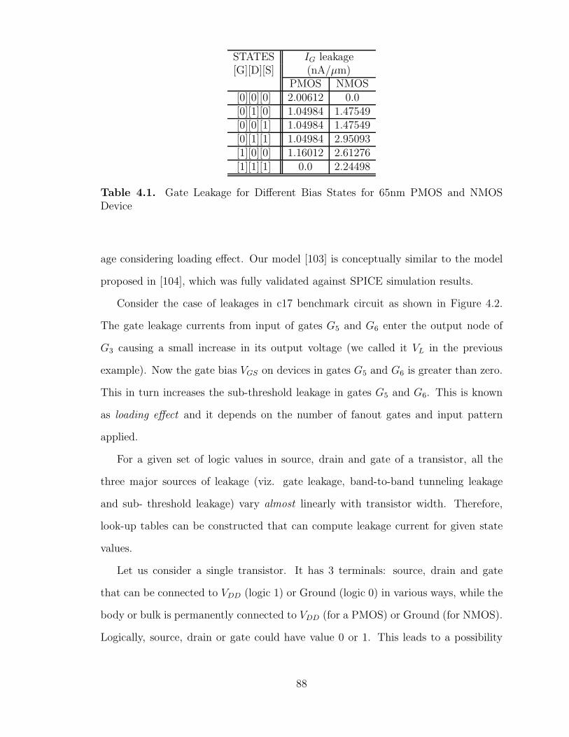
STATES IG leakage[G][D][S] (nA/µm)
PMOS NMOS[0][0][0] 2.00612 0.0[0][1][0] 1.04984 1.47549[0][0][1] 1.04984 1.47549[0][1][1] 1.04984 2.95093[1][0][0] 1.16012 2.61276[1][1][1] 0.0 2.24498
Table 4.1. Gate Leakage for Different Bias States for 65nm PMOS and NMOSDevice
age considering loading effect. Our model [103] is conceptually similar to the model
proposed in [104], which was fully validated against SPICE simulation results.
Consider the case of leakages in c17 benchmark circuit as shown in Figure 4.2.
The gate leakage currents from input of gates G5 and G6 enter the output node of
G3 causing a small increase in its output voltage (we called it VL in the previous
example). Now the gate bias VGS on devices in gates G5 and G6 is greater than zero.
This in turn increases the sub-threshold leakage in gates G5 and G6. This is known
as loading effect and it depends on the number of fanout gates and input pattern
applied.
For a given set of logic values in source, drain and gate of a transistor, all the
three major sources of leakage (viz. gate leakage, band-to-band tunneling leakage
and sub- threshold leakage) vary almost linearly with transistor width. Therefore,
look-up tables can be constructed that can compute leakage current for given state
values.
Let us consider a single transistor. It has 3 terminals: source, drain and gate
that can be connected to VDD (logic 1) or Ground (logic 0) in various ways, while the
body or bulk is permanently connected to VDD (for a PMOS) or Ground (for NMOS).
Logically, source, drain or gate could have value 0 or 1. This leads to a possibility
88
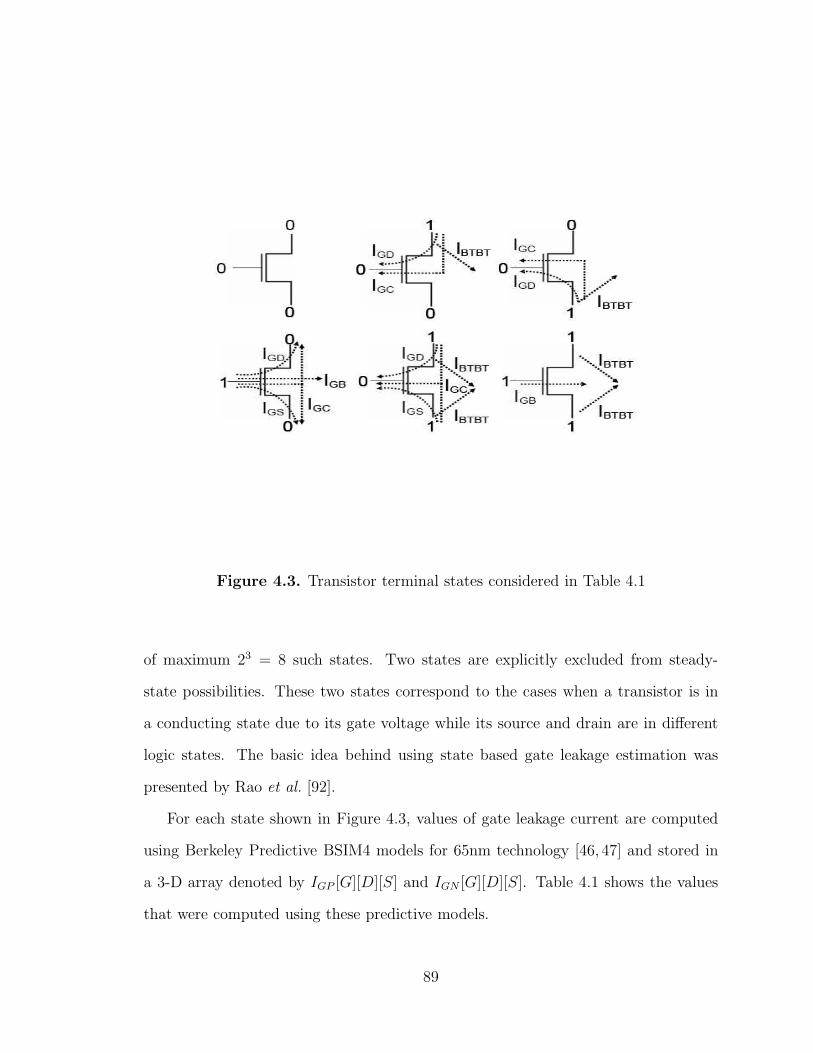
Figure 4.3. Transistor terminal states considered in Table 4.1
of maximum 23 = 8 such states. Two states are explicitly excluded from steady-
state possibilities. These two states correspond to the cases when a transistor is in
a conducting state due to its gate voltage while its source and drain are in different
logic states. The basic idea behind using state based gate leakage estimation was
presented by Rao et al. [92].
For each state shown in Figure 4.3, values of gate leakage current are computed
using Berkeley Predictive BSIM4 models for 65nm technology [46, 47] and stored in
a 3-D array denoted by IGP [G][D][S] and IGN [G][D][S]. Table 4.1 shows the values
that were computed using these predictive models.
89
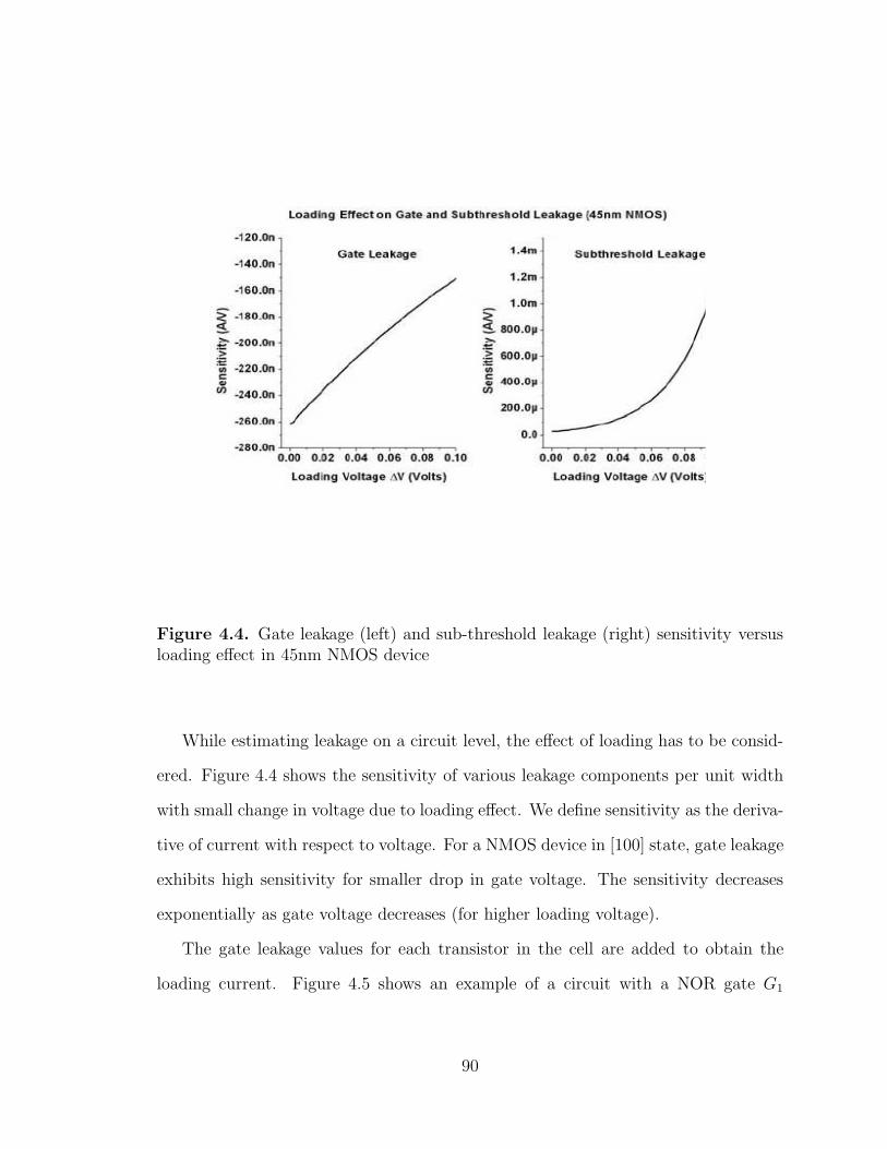
Figure 4.4. Gate leakage (left) and sub-threshold leakage (right) sensitivity versusloading effect in 45nm NMOS device
While estimating leakage on a circuit level, the effect of loading has to be consid-
ered. Figure 4.4 shows the sensitivity of various leakage components per unit width
with small change in voltage due to loading effect. We define sensitivity as the deriva-
tive of current with respect to voltage. For a NMOS device in [100] state, gate leakage
exhibits high sensitivity for smaller drop in gate voltage. The sensitivity decreases
exponentially as gate voltage decreases (for higher loading voltage).
The gate leakage values for each transistor in the cell are added to obtain the
loading current. Figure 4.5 shows an example of a circuit with a NOR gate G1
90
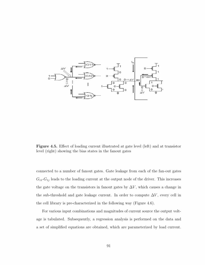
Figure 4.5. Effect of loading current illustrated at gate level (left) and at transistorlevel (right) showing the bias states in the fanout gates
connected to a number of fanout gates. Gate leakage from each of the fan-out gates
G11-G1j leads to the loading current at the output node of the driver. This increases
the gate voltage on the transistors in fanout gates by ∆V , which causes a change in
the sub-threshold and gate leakage current. In order to compute ∆V , every cell in
the cell library is pre-characterized in the following way (Figure 4.6).
For various input combinations and magnitudes of current source the output volt-
age is tabulated. Subsequently, a regression analysis is performed on the data and
a set of simplified equations are obtained, which are parameterized by load current.
91

Figure 4.6. Method to compute loading voltage in a cell using SPICE
More than one equation for each strength of conducting path between cell output and
its power source is needed [15]. Figure 4.5 illustrates how the gate voltage in driver
gates is driven to ∆V . Once the sink current is computed based on gate leakage it
can be translated to ∆V based on the regression equations as mentioned above.
∆V is used to adjust sub-threshold leakage values of the driven gates. Such
adjustments will invariably lead to small changes at output voltages of the driven
gates, which in turn will impact the gate leakage. Newton-Raphson method has been
successfully used in this context [93] and we have incorporated this feature in our
analysis. To account for Newton-Raphson method, loading voltages are re-adjusted
92

in an iterative fashion starting with a baseline value till the difference in ∆V is less
than 5% for two consecutive iterations. Here, instead of using state-based lookup
table as mentioned earlier, we use a set of piece-wise linear equations for gate current
as a function of gate voltage for selected values of drain voltages tuned to deliver
higher accuracy.
4.4.2 Model for Capacitive Crosstalk-induced Noise Current Estimation
There has been a detailed study on developing crosstalk noise model over the last
decade as we have reported in Section 4.2.1. In this thesis, we have adopted a fairly
simple model to compute crosstalk-induced noise current [103], which is conceptually
similar to the model proposed by Devgan [26].
To derive the generalized expression for crosstalk-induced noise current, let us
start with a situation where a victim net (Vi) has two aggressors (Aj and Ak) in the
neighborhood (Figure 4.7). Let the coupling capacitance between the victim Vi and
aggressor Aj be Cij and that with the aggressor Ak be Cik.
Let us assume an input transition in the circuit involving these nets such that the
victim Vi stays in the same logic state 0, whereas both the aggressors (Aj and Ak)
switch from logic state 0 to 1 (as shown in the Figure 4.7). Under this condition, cou-
pling current will flow from the aggressors to the victim net through the appropriate
coupling capacitor.
The coupling current (ic1 and ic2) at an instant t can be expressed as:
ic1(t) = Cijd
dt(VAj
− VVi) (4.1a)
ic2(t) = Cikd
dt(VAk
− VVi) (4.1b)
The total coupling current at the instant t should be obtained by simply adding
the individual coupling current from the aggressors:
93

Figure 4.7. Illustration of an aggressor-victim model used for crosstalk analysis
iC(t) = ic1(t) + ic2(t) = Cijd
dt(VAj
− VVi) + Cik
d
dt(VAk
− VVi) (4.2)
Therefore, in the most general scenario, if a victim net Vi hasm aggressors {A1, A2, . . . , Am}
and under a specific input transition all of these aggressor nets switch from logic state
0 to 1 or from 1 to 0 keeping the victim net silent, the expression for total coupling
current would be:
iC(t) =m
∑
j=1
icj(t) =
m∑
j=1
Cij
dVAj
dt(4.3)
When coupling effect on the aggressor itself is not considered, the termdVAj
dtcan
be simplified as the slew rate corresponding to the rise time (or, fall time) of the
individual aggressor net; i.e. the numerator dVAjcorresponds to the change in voltage
from 0.1 to 0.9 times VDD and the denominator dt is the rise time (trise) or the fall
94

Aggressor Victim k↑ 0 1/Tr
↑ 1 -1/Tr
↓ 0 -1/Tf
↓ 1 1/Tf
Table 4.2. Dependence of k on Various Scenarios of Aggressor Transitions whenVictim Remains Silent at Logic State 0 or 1
time (tfall) associated with it. Accordingly, the generalized expression for coupling
current (iC) can be re-stated as:
iC(t) =m
∑
j=1
Cij0.8VDD
triseAj
= 0.8VDD
m∑
j=1
kijCij (4.4)
where, the term kij depends on the direction of transition of the aggressor j relative
to the victim net i and the corresponding rise time or fall time associated with it as
shown in Table 4.2.
The positive or negative sign on the factor k represents the case when a given
aggressor acts toward contributing or compensating the overall noise.
Moreover, the term k is scaled in a manner proportional to the time difference
between the aggressor and victim transitions as shown in Table 4.2. We consider
a window size of 3 between the aggressor and the victim time slot for a particular
aggressor to be considered for the given victim. Table 4.3 summarizes scaling of the
term k with respect to temporal proximity between an aggressor and a victim.
Expression (4.4) has been used in this thesis to compute coupling current for a
given victim net.
4.4.3 Combined Noise Effect during Signal Integrity Analysis
We use a simple way to find the total noise voltage (VN) induced by loading and
capacitive cross coupling at an instant t. Considering the fact that crosstalk current
95
Distance Between Transitions k(Unit Delay)
0 11 0.662 0.333 0
Table 4.3. Scaling of the k factor
exhibits a transient behavior over a pattern pair whereas gate leakage is a static effect
for a given pattern, we compute crosstalk current (iC) for a given pattern pair and
gate leakage current (iL) for the first pattern of the pair, followed by adding them
together to find the total noise current (iN) at the instant t after application of the
second pattern:
iN (t) = iL(t) + iC(t) (4.5)
After obtaining the total noise current iN , we apply the same regression-fitted
piece-wise linear equations we used to compute loading voltage (as described in Sec-
tion 4.4.1) to obtain the final noise voltage VN .
4.5 Static Analysis of Crosstalk-induced Logic Violations
In this section, we briefly describe a pattern-independent static noise analysis
methodology that flags all the potential logic violations that could be induced solely
by worst case crosstalk noise as well as by the combined effect of worst case crosstalk
and loading in a given circuit with a set of victim nets and their associated aggressors.
During static analysis, we first estimate the worst-case crosstalk noise voltage for
each victim net that could be produced if all the aggressors for the given victim
switch simultaneously in the same direction keeping the victim stay in the same logic
state, followed by evaluating whether this crosstalk noise would cause a logic violation
96

for the given victim. This analysis is clearly pattern-independent as it assumes a
hypothetical worst-case situation. In the second phase, we add the worst case loading
noise contributed by the fan-out gates of the victim to the worst case crosstalk noise
already estimated, to evaluate whether this combined noise effect would cause a logic
violation for the given victim.
4.6 Dynamic Simulation to Evaluate Combined Noise Effect
After obtaining an upper bound on the count of failing victim nets due to crosstalk
and loading from static analysis, we now focus on more detailed pattern-dependent
analysis of the crosstalk related signal integrity problems in presence of aggravating
loading noise on the victim nets [103].
4.6.1 Proposed Dynamic Simulation Technique
The basic principle behind this dynamic simulation strategy is inherently simple
and involves the following five basic steps:
STEP 1: For a given pattern, compute the loading noise current at each internal
node starting from the highest level by traversing backward through the netlist;
STEP 2: Upon application of the second pattern, perform event driven logic simula-
tion. An event-driven simulator follows the path of events. When all the signals
in a circuit are in steady state, if a new vector is applied to primary inputs, some
inputs change, causing events on those input signals. Gates whose inputs now
have events are called active and are placed in an activity list. The simulation
proceeds by removing a gate from the activity list based on a timing wheel and
evaluating it to determine whether its output has an event. A changing output
makes all fan-out gates active, which are then added to the activity list. The
process of evaluation stops when the activity list becomes empty [16, 118]. By
97

the end of this process a list is constructed for all coupled nodes recording the
logic value per interval basis.
STEP 3: For a given victim net, compute the coupling noise current based on how
many aggressors switch per interval and maintain the maximum magnitude of
the noise current over all the intervals. Iterate over STEP 3 for all the victim
nets.
STEP 4: Add the coupling noise current with the loading noise current and compute
the voltage noise i〉 due to only crosstalk, and ii〉 combined effect of crosstalk
and loading;
STEP 5: Update the list of failing nets for i〉 solely crosstalk; and ii〉 combined effect
of crosstalk and loading.
A flowchart description of the methodology is shown in Figure 4.8. If there are k
victim nets for a given circuit, and a total of N input patterns are applied during the
simulation, the upper bound on the time complexity of the simulation technique is
O(k2N).
Since the dynamic simulation is pattern dependent, it implicitly takes care of
the Boolean dependencies between aggressors and the victim in determining which
aggressors may contribute to coupling current. The timing filtering aspect of the
problem is that the aggressors should switch within the same time window to be
considered active for a given victim. We use the activity list constructed during
event-driven simulation to determine which aggressors switch for a given victim net
during a given event interval.
Application of event-driven simulation in this context facilitates us to assume
any non-zero delay model, which, in one hand, eliminates the possibility of over-
estimation of coupling noise by pruning the set of aggressors for a given victim on the
basis of activity recorded per event interval; and at the same time, it also considers the
98
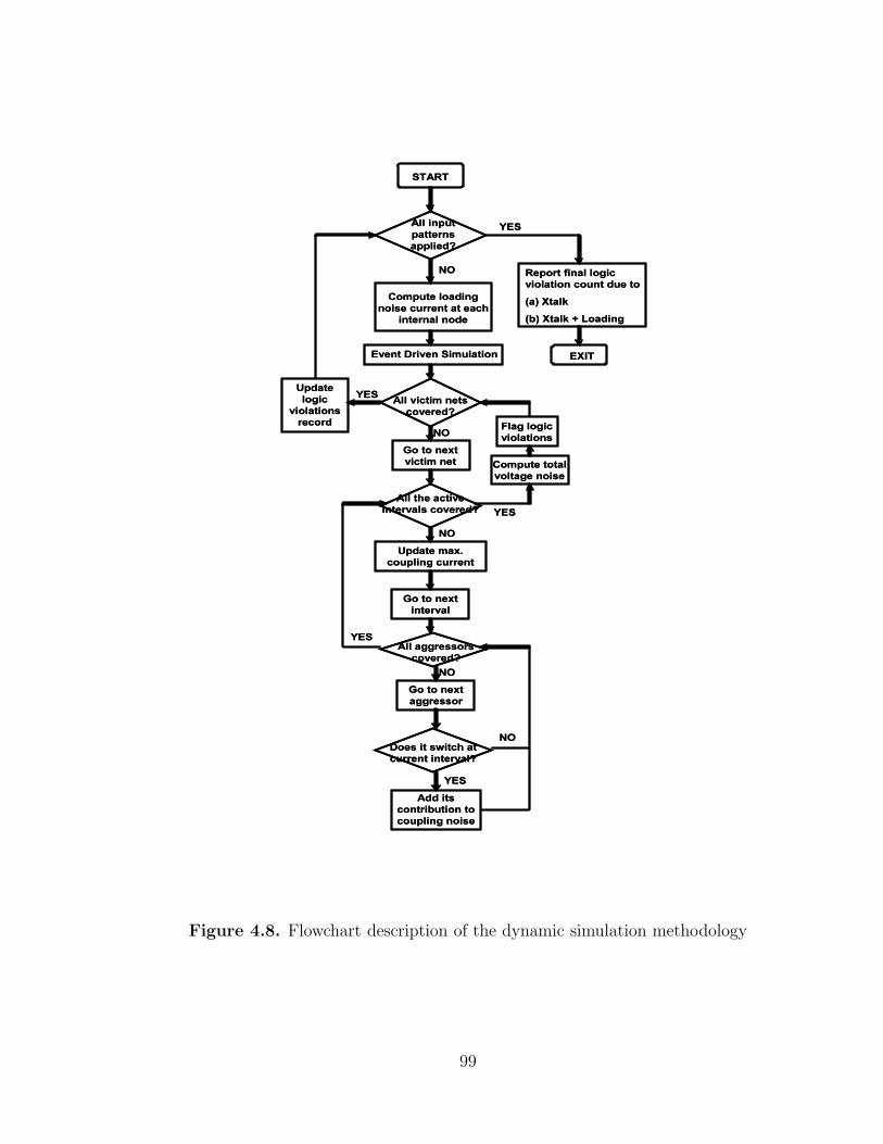
Figure 4.8. Flowchart description of the dynamic simulation methodology
99
contribution of any glitch (0 → 1 → 0 or, 1 → 0 → 1) which would have otherwise
remain un-noticed. Therefore, our signal integrity analysis framework exhibits a
significantly greater level of accuracy.
4.6.2 Limitations of the Proposed Approach
Like all simulation based verification approaches, dynamic simulation cannot guar-
antee discovery of all signal integrity violations. Yet, dynamic simulation based solu-
tions are popular in a number of problems such as in logic verification and in timing
analysis of RAMs. In all of these cases, the formal techniques have capacity and
performance limitations such that they may not terminate in days and weeks or may
run out of memory. In all such cases, simulation provides a viable alternative. Thus,
given the complexity of the problem tackled here, dynamic simulation is the most
practical interim solution until a better solution can be found.
We developed a state-of-the-art simulation tool to show that voltage noise pro-
duced by transistor gate leakage current reduces noise margin for capacitive cross-
coupling induced signal integrity problems in sub-65nm technology nodes. While
the simulator integrates best-of-breed ideas from previous publications, the discovery
of impact of load voltage on signal integrity is a novel contribution. The dynamic
simulation-based study motivates us to propose an automatic test pattern genera-
tion solution that considers the voltage noise caused by gate leakage while generating
worst case pattern pair for crosstalk-related signal integrity problems.
4.7 Pattern Generation to Maximize Combined Noise Effect
The problem of generating a pattern pair that results in maximal voltage noise
due to combined effect of coupling and gate leakage loading in conjunction with
propagating the fault effect to an observable point primarily has the following two
aspects:
100
Goal I: Creation of maximal voltage noise due to coupling and gate leakage loading at
victim: As the victim net is coupled with multiple aggressors, we have to find a subset
of aggressors in temporal proximity with the victim that creates maximal coupling
noise at the victim net. Additionally, the victim fanouts are set to logic states to
maximize loading current at the victim net.
Goal II: Propagation of fault effect to the output: In addition to maximal noise cre-
ation, the pattern pair must also propagate the fault effect at the victim net to an
observation point.
This problem falls into the class of max-satisfiability problems [37]. Max-satisfiability
is a known intractable problem [37]. In this paper we present a complete solution
to the problem by mapping it to an Integer Linear Programming (ILP) formulation.
Thus given enough time, we will be able to obtain an input pattern pair that leads to
absolute worst case voltage noise due to combined effect of crosstalk and gate leakage
loading on a given victim net.
Given a set of m aggressors {A1, A2, · · · , Am} coupled with a victim V and a set
of n fanout gates {F1, F2, · · · , Fn} driven by it, we perform the following two steps.
4.7.1 Circuit Transformation
4.7.1.1 Time Domain Expansion to Incorporate Gate Delays
It has been shown previously that gate delay plays an important role in the context
of crosstalk related signal integrity analysis [35]. In this paper, we assume unit gate
delay model. We assume that it takes 1 unit of time between 50% transition of the
input to the 50% transition of the output for any given gate. Unit gate delay model
allows arbitrary integer delays through circuit transformation that adds buffer chain.
Consideration of delays allows temporal proximity between an aggressor and a victim
to be considered, improving the quality of the solution. If an aggressor does not
101
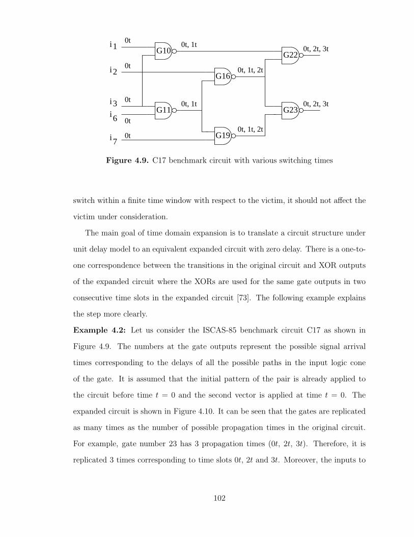
G10
G11
i
i
i
2
6
7
i 3
i 1
G16
G19
G23
G220t
0t
0t
0t
0t
0t, 1t
0t, 1t
0t, 1t, 2t
0t, 1t, 2t
0t, 2t, 3t
0t, 2t, 3t
Figure 4.9. C17 benchmark circuit with various switching times
switch within a finite time window with respect to the victim, it should not affect the
victim under consideration.
The main goal of time domain expansion is to translate a circuit structure under
unit delay model to an equivalent expanded circuit with zero delay. There is a one-to-
one correspondence between the transitions in the original circuit and XOR outputs
of the expanded circuit where the XORs are used for the same gate outputs in two
consecutive time slots in the expanded circuit [73]. The following example explains
the step more clearly.
Example 4.2: Let us consider the ISCAS-85 benchmark circuit C17 as shown in
Figure 4.9. The numbers at the gate outputs represent the possible signal arrival
times corresponding to the delays of all the possible paths in the input logic cone
of the gate. It is assumed that the initial pattern of the pair is already applied to
the circuit before time t = 0 and the second vector is applied at time t = 0. The
expanded circuit is shown in Figure 4.10. It can be seen that the gates are replicated
as many times as the number of possible propagation times in the original circuit.
For example, gate number 23 has 3 propagation times (0t, 2t, 3t). Therefore, it is
replicated 3 times corresponding to time slots 0t, 2t and 3t. Moreover, the inputs to
102
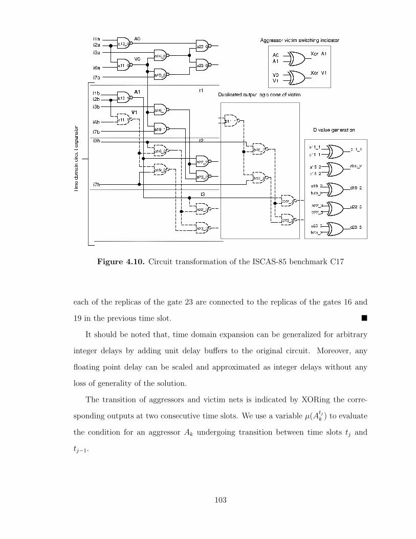
Figure 4.10. Circuit transformation of the ISCAS-85 benchmark C17
each of the replicas of the gate 23 are connected to the replicas of the gates 16 and
19 in the previous time slot. �
It should be noted that, time domain expansion can be generalized for arbitrary
integer delays by adding unit delay buffers to the original circuit. Moreover, any
floating point delay can be scaled and approximated as integer delays without any
loss of generality of the solution.
The transition of aggressors and victim nets is indicated by XORing the corre-
sponding outputs at two consecutive time slots. We use a variable µ(Atjk ) to evaluate
the condition for an aggressor Ak undergoing transition between time slots tj and
tj−1.
103
4.7.1.2 Fault Effect Propagation
We perform circuit transformation in the output logic cone of the victim net in
order to generate conditions for fault effect propagation. In this step the output logic
cone including the victim is duplicated. The original logic cone represents the good
machine while the duplicated logic cone represents the faulty machine. In addition,
a D value is generated for each gate in the fault propagation cone by XORing the
corresponding gate outputs of the two logic cones. A D value represents the case
where the faulty value and good value are different i.e. the fault effect is being
propagated. ILP formulation is done subsequently to propagate the D value from
victim net to the primary outputs. The following example helps understand the step.
Example 4.3: In Figure 4.10, the output logic cone of the victim net a11 1 (where
a11 is gate number and 1 is the time slot of the gate) is represented using broken
line. The duplicated gates are renamed by replacing the prefix a with b. Inputs to the
duplicated gates which are not a part of the output logic cone of the victim net are
supplied from the corresponding gates in original circuit. For example, for the gate
b22 3 in the duplicated circuit, the input (represented by a continuous line) which is
not a part of the output logic cone of the victim comes from the gate a10 1 of the
original circuit. Fault effect propagation is indicated by XORing the corresponding
outputs of the original and the duplicate circuits to generate D value. For example,
the nets a16 2 and b16 2 are XORed to obtain D value of d16 2. ILP formulation is
done using D values for fault propagation. �
4.7.2 ILP Formulation
In order to obtain the maximal noise due to combined effect of crosstalk and
gate leakage loading for a given victim net in a circuit, ILP formulation is done for
the circuit by writing the ILP equations for the logic gates [32], which are formed by
using the clausal description of the function of the gates as developed by Larrabee [66].
104

ba
c
d
e
f
Figure 4.11. An example combinational logic block
For example for an AND gate with inputs a, b and output c, we can describe all 4
input-output combinations as presented in equations 6(a)-6(d).
a⇒ c or a + (1− c) ≥ 1 (4.6a)
b⇒ c or b+ (1− c) ≥ 1 (4.6b)
ab⇒ c or (1− a) + (1− b) + c ≥ 1 (4.6c)
a, b, c ∈ [0, 1] (4.6d)
For the circuit shown in Figure 4.11 the complete set of ILP equations are presented
in Equations 7(a)-7(h).
d+ f ≥ 1 (4.7a)
e+ f ≥ 1 (4.7b)
(1− d) + (1− e) + (1− f) ≥ 1 (4.7c)
c+ e = 1 (4.7d)
(1− a) + d ≥ 1 (4.7e)
(1− b) + d ≥ 1 (4.7f)
a+ b+ (1− d) ≥ 1 (4.7g)
105

a, b, c, d, e, f ∈ [0, 1] (4.7h)
With a brief discussion on ILP formulation using clausal description of the func-
tionality of different gates, we now focus on developing the constraints for (a) switch-
ing of aggressors in a way that causes maximal crosstalk noise at the output of a given
victim net keeping the victim silent at either logic state 0 or 1; (b) set the fan-outs of
the victim in such a state that it causes maximal loading noise at the victim; and (c)
assuming the cumulative voltage noise causes a logic violation at the fan-out stage,
propagate the fault effect to an observation point.
We assume a set of m aggressors {A1, A2, · · · , Am} coupled with a victim V and
a set of n fanouts {F1, F2, · · · , Fn} associated with them. Suppose there are K copies
of the victim present in the expanded circuit starting from the time slot S to time
slot T . The variable representing the victim V at time slot i is denoted XV i. For the
crosstalk pulse problem, we consider the victim to be static either at logic state 0 or
1. The following constraint represents this condition:
Constraint 1: Victim static at its logic state for any two consecutive time slots i and
i− 1:
XV i −XV i−1 = 0 ∀i = S + 1, · · · , T (4.8)
4.7.2.1 Constraints for Maximal Crosstalk Noise
We consider any aggressor Ak which makes a transition (either 0 → 1 or 1 → 0)
at time slot j within a time window of 2 with respect to the victim’s current time slot
i toward computing the cumulative coupling noise and define a variable µ(Ajk) such
that:
µ(Ajk) = XAj
k ⊕XAj−1k ∀i, j : |j − i| ≤ 2 (4.9)
where, the variable representing the aggressor Ak at time slot j is denoted as XAjk.
We also define a variable λ(Ajk;Vi) to represent the condition that the final value of
the aggressor Ak at time slot j and the victim V at time slot i are opposite:
106

λ(Ajk;V
i) = XAjk ⊕XV
i ∀i, j : |j − i| ≤ 2 (4.10)
To determine whether a given aggressor transition acts toward contributing or com-
pensating the cumulative coupling noise, we propose the following two constraints:
Constraint 2: If a given aggressor Ak switches at time slot j such that the final logic
value of the aggressor at time slot j and the victim at time slot i are different, the
aggressor is said to contribute to the cumulative coupling noise.
We express this constraint with the aid of the variable φ(Ajk;V
i) in the following
way:
φ(Ajk;V
i) = µ(Ajk) • λ(Aj
k;Vi) (4.11)
Constraint 3: If a given aggressor Ak switches at time slot j such that the final logic
value of the aggressor at time slot j and the victim at time slot i are same, the
aggressor is said to act toward compensating the cumulative coupling noise.
We express this constraint with the aid of the variable ψ(Ajk;V
i) in the following
way:
ψ(Ajk;V
i) = µ(Ajk) • λ(Aj
k;Vi) (4.12)
With the aid of constraints 2 and 3 defined above, we may now express the equation
(4) describing the cumulative coupling noise caused by a set of m aggressors for a
given victim V at the time slot tc in the following way:
iC(V tc) = 0.8VDD
m∑
j=1
(φ(Ajk;V
i) ·1
Tr
− ψ(Ajk;V
i) ·1
Tf
) · CAk V (4.13)
4.7.2.2 Constraint for Maximal Gate Leakage Loading Noise
We now explain the formulation of ILP constraints that maximizes gate leakage
from fanout nodes for a given victim net. After the circuit expansion step, a gate
is replicated into various time slots. The idea here is to create appropriate input
condition at the fanout nodes of a given victim to cause gate leakage loading from the
107

fanouts together with capacitive coupling induced signal noise through switching of
the aggressor net(s) for the victim net, at the same time slot. In order to maximize
the effect of gate leakage loading, the inputs of the fanout gates of the victim should
be set appropriately. The following example illustrates the point:
Example 4.4: Let us consider a victim net V at the time slot tc for an example
time-expanded circuit shown in Figure 4.12. The instance of the two fanout gates F1
and F2 for the victim copy at time slot tc appear in next two time slots tn1and tn2
respectively in the time-expanded circuit. To enforce maximum gate leakage loading
at the victim net V at current time slot tc, the inputs to these two fanout instances
should be set in such a way so as to obtain maximal gate leakage loading at the victim
net V at time slot tc. As shown in Figure 4.12, the side input S1 of fanout instance
of F1 at time slot tn1appears in the previous time slot tp. The side input S2 for the
instance of fanout F2 at time slot tn2appears in the current time slot tc. The ILP
formulation is done for the input and output logic cones of victim V and the input
logic cone of the side input gates S1 and S2. �
Constraint 4: In order to generate the ILP equations for leakage current, Boolean
variables indicating all the possible input combinations of the victim’s fanout gates
are generated. Then the total leakage is expressed as a linear combination of the
binary variables representing individual input condition weighted by corresponding
logic states’ leakage weight. For example, for the circuit shown in Figure 4.12, gates
F1tn1 and F2tn2 will be considered for leakage at the victim net V at time slot tc. We
define binary variables l00, l01, l10, and l11 corresponding to every possible input
condition for the fanout gates F1 and F2 as follows:
l00tn1
F1 = (S1tp ∧ V tc) (4.14a)
l01tn1
F1 = (S1tp ∧ V tc) (4.14b)
l10tn1
F1 = (S1tp ∧ V tc) (4.14c)
108

PreviousTime Slot
Time SlotCurrent
NextTime Slots
t
t
t
t
c
p
n1
n2
time slotVictim at current
Side inputs of
of victim V
the fanouts
Fanout gates
S1tp
S2tc
Vtc
F2tn2
F1tn1
Figure 4.12. Illustration of gate leakage loading from fanout nodes of a victim V attime slot tc
l11tn1
F1 = (S1tp ∧ V tc) (4.14d)
LtcF1 = l00
tn1
F1 ·Wt00F1 + l01tn1
F1 ·Wt01F1 + l10tn1
F1 ·Wt10F1 + l11tn1
F1 ·Wt11F1 (4.14e)
l00tn2
F2 = (S2tc ∧ V tc) (4.14f)
l01tn2
F2 = (S2tc ∧ V tc) (4.14g)
l10tn2
F2 = (S2tc ∧ V tc) (4.14h)
l11tn2
F2 = (S2tc ∧ V tc) (4.14i)
LtcF2 = l00
tn2
F2 ·Wt00F2 + l01tn2
F2 ·Wt01F2 + l10tn2
F2 ·Wt10F2 + l11tn2
F2 ·Wt11F2 (4.14j)
In the equations (14e) and (14j), the variables LtcF1 and Ltc
F2 represent the gate leakage
loading at victim V at time slot tc coming from the fanout gates F1 at time slot tn1
and F2 at time slot tn2respectively.
109

Therefore, the general expression for total gate leakage loading noise current over
the entire set of fanout gates for a given victim V at time slot tc is:
iGL(V tc) =∑
Fg∈FO(V tc)
LtcFg
(4.15)
where, FO(V tc) is the set of fanout gates for the given victim net V at time slot tc.
4.7.2.3 Objective Function for the Combined Signal Noise
The cumulative noise on a given victim net V due to capacitive cross-coupling
with neighbor aggressor nets as well as gate leakage loading from its fanout gates at
a given time slot tc is expressed as:
iN(V tc) = iC(V tc) + iGL(V tc) (4.16)
Therefore, the objective function would be to maximize the cumulative noise iN (V tc)
over all the time slots S to T when the victim V is active:
maximize Obj = iN (V tc) ∀tc = S, · · · , T (4.17)
4.7.2.4 Constraints for Fault Effect Propagation
To ensure the propagation of the fault effect from the output of the victim net to
a primary output, we create a duplicate copy of the output logic cone of the victim
V , which represents the “faulty” value XKif for any given gate K at the output logic
cone of the victim at time slot i. The “good” value of the gate K is represented by
XKig. The XOR of the “good” value and the “faulty” value at time slot i, represented
110

by the D value DKi will propagate the fault effect from the victim V through the
gate K on its output logic cone:
DKi = XKig ⊕XK
if (4.18)
The following two constraints ensure that if a logic violation is observed at the output
of a victim V , it will propagate to at least one primary output.
Constraint 5: Logical OR of D value of all the primary outputs Zk ∈ PO will be 1:
∨
Zk∈PO
DZk = 1 (4.19)
where, PO is the set of all primary outputs.
Constraint 6: A D value at a gate output implies that at least one of the gate inputs
in the output logic cone of the victim net V has a D value.
Therefore, for a gate K at time slot i with inputs K1 at time slot i1 and K2 at
time slot i2, the following implication formally expresses the above constraint:
DKi ⇒ DKi11 ∨DK
i22 (4.20)
Finally, in order to initiate fault effect generation at the victim net, a D value has to
be enforced at all the copies of the victim net Vj starting from the first copy of the
victim at time slot S to final copy at time slot T .
111

4.7.3 ILP-based Test Pattern Generation Algorithm
Algorithm 1 MaxSignalNoiseATPG (C, V )
1: Sx ← {∅}2: Tx ← {∅}3: Sxl ← {∅}4: Txl ← {∅}5: LogicViolation ← 06: for each member v ∈ V do7: LogicViolation ← MaximizeXtalkNoise(v, A[v])8: if (LogicViolation == TRUE and
PropagateFaultEffect(v) == TRUE) then9: Sx ← Sx
⋃
{v}10: Tx ← Tx
⋃
{〈p1, p2〉}11: end if12: LogicViolation ← MaximizeCombinedNoise(v, A[v], F [v])13: if (LogicViolation == TRUE and
PropagateFaultEffect(v) == TRUE) then14: Sxl ← Sxl
⋃
{v}15: Txl ← Txl
⋃
{〈p1, p2〉}16: end if17: end for18: return |Sx| and |Sxl|
After establishing an Integer Linear Program (ILP)-based formulation of an ob-
jective function aimed at maximizing the combined noise effect due to 〈i〉 capacitive
interference between neighbor interconnects, and 〈ii〉 gate leakage-induced loading
from fanout nodes, we now formally present the test pattern generation algorithm
MaxSignalNoiseATPG(), which accepts a circuit description C and a list of capaci-
tively coupled interconnect nets V as input arguments. The objective of this algo-
rithm is to separately generate a pair of test patterns 〈p1, p2〉 that maximizes (a) the
capacitive crosstalk noise, and (b) combined signal noise on a given net.
Algorithm 1 presents a pseudo-code description of the ATPG algorithm. We
begin with initializing sets Sx and Sxl, which are used to store the failing nets due to
crosstalk and combined noise effect respectively. The sets Tx and Txl are used to store
the respective test pattern pairs for these failing nets. The variable LogicViolation
112
is used as a flag to indicate whether the noise produced at a given interconnect net by a
pattern pair crosses the logic switching threshold of its fanout stage. For each member
v of the set of coupled nets V , we invoke the procedure MaximizeXtalkNoise()
that first constructs an ILP-based model aimed at maximizing the crosstalk noise,
followed by evaluating whether the crosstalk-induced signal noise exceeds the logic
switching threshold of the fanout stage thereby causing a logic violation (line 7). If the
variable LogicViolation is set to TRUE and the procedure PropagateFaultEffect()
finds a sensitized path from the net v to an observation point (line 8), then the
given net v is included in the set Sx of crosstalk-induced failing nets (line 9) and
the corresponding test pattern pair is included in the set Tx (line 10). Similarly,
the procedure MaximizeCombinedNoise() evaluates whether it is possible to cause a
logic violation at a given net v due to combined noise effect (line 12). If the variable
LogicViolation is set to TRUE and the procedure PropagateFaultEffect() finds
a sensitized path from the net v to an observation point (line 13), then the given
net v is included in the set Sxl of combined noise-induced failing nets (line 14) and
the corresponding test pattern pair is included in the set Tx (line 15). Finally, the
cardinality of the sets Sx and Sxl are computed and reported (line 17).
The proposed algorithm retains the completeness of the solution in the sense that,
given enough time and space, it will find out the pattern pair 〈p1, p2〉 that causes
maximal noise condition on a given interconnect net and evaluates the existence of
a sensitized path from the fault site to an observation point to propagate the fault
effect. Therefore, given a set V of coupled nets for a given circuit C, the proposed
technique identifies a subset V ′ ⊂ V of failing nets and their respective tests T [V ′].
In the next sub-section, we address the scalability issues involved with the proposed
solution.
113

4.7.4 Scalability of the Proposed ATPG Solution
In this section, we show that the proposed solution is highly scalable. We present
the scalability of this approach in terms of crosstalk ATPG performance, resulting
size of the test set and ability to handle non-unit gate delays.
4.7.4.1 Performance
Scalability of the solution is related to the number of ILP equations for an individ-
ual instance of the problem. Fewer the number of equations, greater is the likelihood
of finding an exact solution. The number of equations in turn relate to the cone of
logic needed to formulate justification and propagation conditions for the crosstalk
fault as shown in Figure 4.13, which in turn relates to logic depth. It has been noted
that, in modern designs the logic depth tends to be shallow: typically 6-8 levels of
logic gates [44]. Also, in CMOS circuits, the number of fan-ins is limited due to non-
linear increase in gate delay with transistor stack height. Typically, the number of
fan-in in CMOS gates is limited to 4 [91]. Thus the number of gates in a logic cone in
a circuit of logic depth l and fan-in of f is of the order of O(
f l)
. When the unit delay
model is considered, worst case size of such logic cone is of the order of O(
l · f l)
.
In ISCAS circuits, the logic depth tends to be much greater. In fact for C3540, for
which we had the worst case CPU time (as shown in Table 4.4 and plot presented in
Figure 4.14), the logic depth is 47. The logic cone of interest is correspondingly much
larger than expected logic cone size of modern designs leading to a significantly high
run time. The circuit C6288 is a 16-bit multiplier and stands as a nemesis case for
ILP-based approach. We observe a time-out for each of the 33 capacitively coupled
nets for this circuit. It may be of interest to note that in circuits where the total gate
count was larger than C3540, but the combinational logic depth was smaller (such as
C5315 and C7552), the worst case CPU time reported was actually lower compared
114

Figure 4.13. Illustration showing the logic cones of interest for a typical instance ofthe ATPG problem
to the case for C3540 (as shown in the plot in Figure 4.14) for the reasons described
above.
4.7.4.2 Test Compression
A notable benefit of the proposed approach is in test compression. Test com-
pression works best when some of the inputs in a test vector are not specified. In a
multi-million gate design, the logic cone of interest includes only a small fraction of
the inputs. Since ILP formulation does not include inputs outside the cone of interest,
115
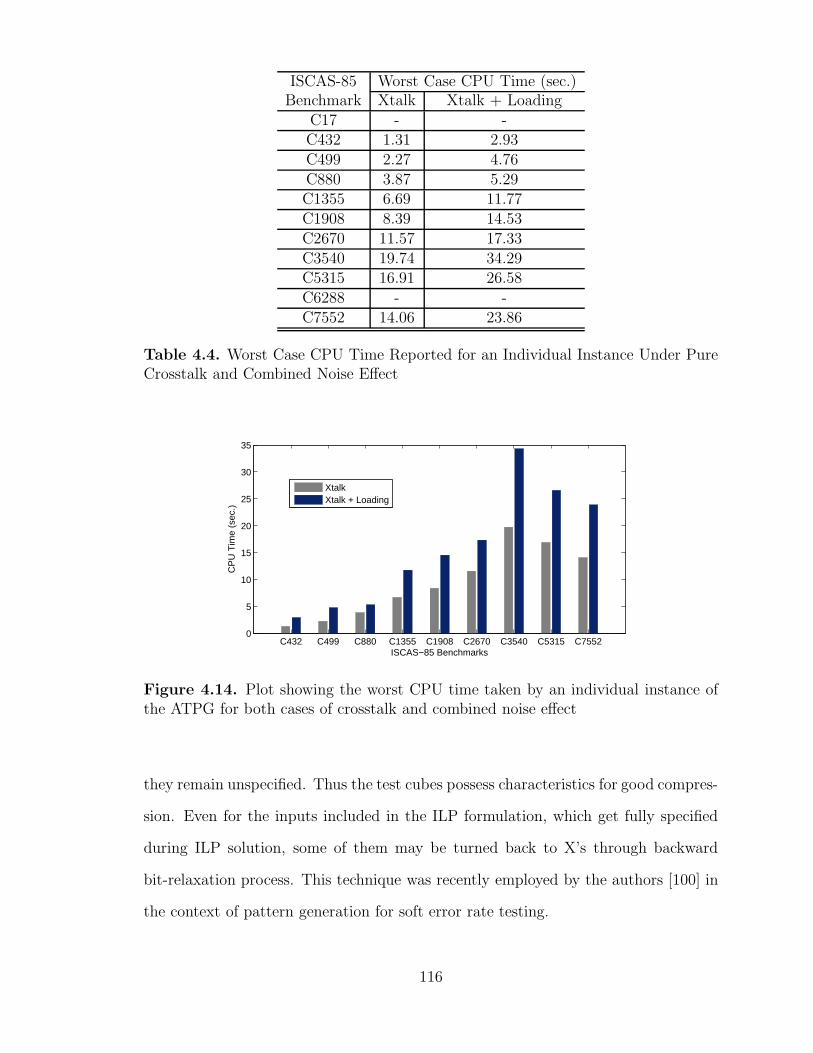
ISCAS-85 Worst Case CPU Time (sec.)Benchmark Xtalk Xtalk + Loading
C17 - -C432 1.31 2.93C499 2.27 4.76C880 3.87 5.29C1355 6.69 11.77C1908 8.39 14.53C2670 11.57 17.33C3540 19.74 34.29C5315 16.91 26.58C6288 - -C7552 14.06 23.86
Table 4.4. Worst Case CPU Time Reported for an Individual Instance Under PureCrosstalk and Combined Noise Effect
C432 C499 C880 C1355 C1908 C2670 C3540 C5315 C75520
5
10
15
20
25
30
35
ISCAS−85 Benchmarks
CP
U T
ime
(sec
.)
XtalkXtalk + Loading
Figure 4.14. Plot showing the worst CPU time taken by an individual instance ofthe ATPG for both cases of crosstalk and combined noise effect
they remain unspecified. Thus the test cubes possess characteristics for good compres-
sion. Even for the inputs included in the ILP formulation, which get fully specified
during ILP solution, some of them may be turned back to X’s through backward
bit-relaxation process. This technique was recently employed by the authors [100] in
the context of pattern generation for soft error rate testing.
116

4.7.4.3 Beyond Unit Delay
If gates in a circuit have integer delays, they can easily be converted to unit delay
circuit using miter gates. For example, if a NAND gate has delay of 3, we can insert
two buffers between NAND gate output and its fanouts. If all gates in the new circuit
have unit delay, it has the equivalent behavior of the original circuit. Please note
that this will not increase the number of equations in our formulation. The solution
extends to circuits with real delays that can be normalized to have equivalent integer
delays.
4.8 Experimental Results
We evaluated the effectiveness of the dynamic simulation-based study and the
proposed test pattern generation algorithm on ISCAS-85 combinational benchmark
suite.
4.8.1 Experimental Setup
Computation of the loading effect requires a number of look-up tables on a per cell
basis. To keep this computation simple, as well as fully validated, all the benchmark
circuits were initially mapped to a cell library consisting of only NOR2 cell. The logic
switching threshold for individual inputs of the NOR2 cell was obtained by running
HSPICE [2] using 65nm BPTM model [47]. Subsequently, a look-up table was created
to store the logic switching threshold for the two inputs of the NOR2 cell.
The parasitic RC data for 250nm technology were extracted in SPEF format us-
ing Cadence SOC Encounter tool [31] and subsequently scaled down to 65nm process.
The SPEF files were parsed to list only the victim-aggressor information with asso-
ciated coupling capacitance values. The ATPG-related experiments used an open
source linear program solver, GNU Linear Programming Kit (GLPK) [55] with a user
specified time limit for each instance of the ILP. The platform for these experiments
117
was a Dell PowerEdge 2800 server [1] with 2.8GHz dual core Intel Xeon processor,
2MB L2 cache and 2GB RAM.
In the following two sub-sections, we present and analyze the results obtained
for the dynamic simulation-based evaluation of influence of gate leakage loading on
aggravating capacitive crosstalk-induced voltage noise, and the subsequent ATPG
solution that aims at maximizing the combined noise effect.
4.8.2 Results for Dynamic Simulation-based Study
Pattern-dependent dynamic simulation was carried out on all ISCAS-85 bench-
mark circuits. Computation of the loading effect requires a number of tables on a
per cell basis. To keep this computation simple, as well as fully validated, all the
benchmark circuits were initially mapped to a cell library consisting of only NOR2
gate.
The experiments broadly involved the following three phases:
4.8.2.1 Parasitic RC Extraction
The parasitic RC data for 250nm technology were extracted in SPEF format using
CadenceTM SoC Encounter tool and scaled for 65nm process [31]. This is because
we did not have access to 65nm layout rules. The SPEF files were parsed to list only
the victim-aggressor information with associated coupling capacitance values.
4.8.2.2 Extraction of Slew Data
The rise and fall slews at every net in the circuit were obtained by performing
static timing analysis using SynopsysTM PrimeTime [90] based on cell library char-
acterization using BPTM models [46, 47].
118

Failing Net Count
ISCAS-85 Number of Static Analysis Dynamic Analysis
Benchmarks Coupled Logic Filtering Logic+Timing Filtering
Nets Xtalk Xtalk + Xtalk Xtalk + Xtalk Xtalk +
Loading Loading Loading
C17 0 - - - - - -
C432 5 3 5 2 2 2 2
C499 9 6 9 4 5 3 3
C880 5 4 5 3 3 1 2
C1355 9 7 9 4 5 2 3
C1908 22 18 22 14 16 9 11
C2670 34 29 34 24 27 21 23
C3540 62 60 62 51 57 37 41
C5315 97 88 97 74 81 63 68
C6288 33 33 33 28 31 21 24
C7552 85 60 85 47 53 38 42
Total Violation Count 308 361 251 280 197 219
Table 4.5. Dynamic Simulation-based Signal Integrity Analysis Results for ISCAS-85 Benchmark Circuits
4.8.2.3 Pattern-dependent Dynamic Simulation
Apart from static simulation, that gives us an upper bound on number of failing
nets, we applied 10,000 random input patterns to each circuit for identifying failing
nets under pattern dependent dynamic environment. Table 4.5 summarizes our find-
ings. For each circuit, we report the total number of victim nets, an upper bound on
crosstalk-induced logic violations as obtained through static analysis, and pattern-
dependent count on logic violations due to a〉 only crosstalk and due to b〉 combined
effect of crosstalk and loading as obtained from dynamic simulation. These figures
are reported when only implicit logic filtering is considered, and as well as when both
logic and timing filtering are considered.
From Table 4.5 we observe that for larger ISCAS-85 benchmarks involving con-
siderable number of coupled nets, loading-induced voltage noise causes more number
of coupled nets to fail compared to the case when we consider crosstalk-induced volt-
119
age noise alone. We also observe that loading-induced voltage noise flags more logic
violations as shown in Table 4.5.
4.8.3 ATPG Results
As the CMOS technology moves deeper into nanometer regime, sharper signal
transitions and reduction of device noise margin by various sources of noise start
playing an important role in signal integrity analysis. As a first attempt to examine
the combined effect of different noise sources, we performed the dynamic simulation-
based study to establish the importance of considering gate leakage induced loading
noise while performing signal integrity analysis for nano-scale CMOS designs [103].
However, dynamic simulation has the following two drawbacks: i〉 it is not compre-
hensive from test point of view as there could be cases of violating conditions that
could lead to identifying a new set of failing nets, that are not exercised by the
set of random patterns applied; and ii〉 dynamic simulation aims at identifying nets
that, under the effect of noise, exceed the logic switching threshold of their respec-
tive fanout gates and therefore, cause logic violations at the fanout stage. However,
dynamic simulation does not ensure that a logic violation, from the fanout stage, will
propagate to an observation point and get recorded as an error.
Motivated by the need for a test solution, we next propose an ILP-based pattern
generation technique for detection of noise pulses caused by the combined effect of
capacitive cross-coupling between neighbor nets and gate leakage induced loading
noise from fanout nodes of a given driver net.
In practice, we maintained a time limit of 1 hour for every single instance of ATPG
for maximizing the crosstalk noise and a time limit of 2 hours for the corresponding
instance for combined noise effect due to crosstalk and leakage loading. This difference
in time allocation for the two separate cases of optimization is based on the fact that
the computation time needed by the ILP solver is directly related to the number of
120

Proposed ATPG
ISCAS-85 Coupled Xtalk Xtalk + Loading
Benchmarks Nets Fault Proven Abort Fault Proven Abort
Detected Unobservable Detected Unobservable
C17 0 - - - - - -
C432 5 1 1 0 2 0 0
C499 9 1 2 0 2 1 0
C880 5 0 1 0 1 1 0
C1355 9 1 0 1 2 0 1
C1908 22 5 2 2 8 0 3
C2670 34 9 10 2 14 4 5
C3540 62 11 13 13 18 5 18
C5315 97 29 28 6 37 20 11
C6288 33 - - 33 - - 33
C7552 85 23 6 9 35 4 3
Table 4.6. Signal Integrity ATPG Results for ISCAS-85 Benchmark Circuits
constraints used by an individual instance of the optimization problem. Since the
problem instance for combined noise effect includes the constraints for gate leakage
loading as well, it is a prudent decision to allocate a higher time limit for the case
of combined noise effect. Table 4.6 summarizes the results obtained for ISCAS-85
benchmark circuits. Column 2 reports the total number of coupled nets in a given
design. We ran ILP-based test generation algorithm for every single coupled net for
a given design. For the proposed ATPG-based approach, three distinct possibilities
exist: 〈i〉 a pattern pair is found that detects the fault at an observation point, 〈ii〉
the ILP returns a no solution which implies that there exists no pattern pair that
can simultaneously create a fault effect and propagate it to an observation point, and
〈iii〉 the ILP solver runs out of maximum allocated time to solve a single instance of
the problem. We report results for these three possibilities in three separate columns
both for the cases of crosstalk-induced noise and the combined noise effect due to
crosstalk and loading. We observe that considering noise from both crosstalk and
gate leakage loading can detect up to 64% more faults (column 6) as compared to the
121

crosstalk-only case (column 3). Columns 5 and 8 reports the number of instances the
ILP solver runs out of the maximum allocated time. The benchmark C6288 presents
a nemesis case for the ATPG problem, and we observe that the ILP solver ran out of
allocated time for each of the instances of capacitively coupled nets.
4.9 Conclusions and Future Directions
In this chapter, we first studied the impact of loading effect on capacitive crosstalk
related signal integrity analysis. A novel dynamic timing simulator was devised to
handle both crosstalk noise and transistor gate leakage noise together. The simulator
was validated against available systems. It was shown that loading effect worsens
crosstalk noise by more than 10%. The problem becomes more severe for larger cir-
cuits. This dynamic simulation-based study emphasizes the fact that loading effect
must be considered during crosstalk related signal integrity analysis both for verifi-
cation as well as manufacturing test.
Motivated by the need for considering gate leakage loading during signal integrity
testing, we next proposed an automatic test pattern generation (ATPG) algorithm
that uses 0-1 Integer Linear Program (ILP) to attain the goals of i〉 formulating an
objective function for maximizing combined signal noise due to crosstalk and leakage
loading, and ii〉 finding a sensitized path from the given victim net to an observation
point. Events triggered by this ATPG patterns will propagate to an observation
point, making them useful for both manufacturing test application as well as signal
integrity verification. The proposed ATPG is capable of handling logic dependencies
as well as temporal proximity effects as modeled by integer delays.
This research opens up a new direction for studying nanometer noise effects and
motivates us to extend the study to other noise sources in tandem including voltage
drop and temperature effects.
122
CHAPTER 5
CONCLUSIONS
Intermittent failures occurred at certain Process-Voltage-Temperature (PVT) con-
ditions during functional operation largely outnumber the permanent failures intro-
duced during manufacturing process, as we move deep into nanometer technology.
Therefore, it is of paramount importance to come up with efficient test generation
and test application methods to accurately detect and characterize these classes of
failures.
In this thesis, we primarily focused on a thorough and integrated study on testing
different intermittent error mechanisms and addressed three distinct problems related
to 〈i〉 soft-error modeling and soft-error characterization test development, 〈ii〉 testing
circuit-marginality related to thermal and voltage aberration conditions, and 〈iii〉
signal integrity analysis and testing considering multiple aggressor crosstalk fault in
presence of leakage loading effects.
Soft-error is a rising technology and design concern. Despite decades of develop-
ment, soft-error rate characterization remains a slow and expensive process. In this
thesis, we proposed a two step approach: 〈i〉 a new filtering technique based on am-
plitude of the noise pulse, which significantly reduces the set of soft-error susceptible
nodes to be considered for a given design, followed by 〈ii〉 an Integer Linear Program
(ILP)-based pattern generation technique that accelerates the SER characterization
process by 1-2 orders of magnitude compared to the current state-of-the-art.
Process-Voltage-Temperature (PVT) excursion has emerged as a dominant con-
cern in contemporary research. Unfortunately, there are no effective fault models
123
for testing failures due to temporary rise in temperature or instantaneous voltage
drop that results from a combination of factors. In this thesis, we proposed a novel
design-for-testability technique that facilitates application of pseudo-random patterns
to effectively detect and isolate different classes of such intermittent errors as opposed
to permanent errors. We also showed a simple extension of the proposed BIST-based
DFT method to handle application of deterministic test patterns.
A major contribution of this thesis lies on investigating the effect of multiple
sources of noise acting together in exacerbating the noise effect even further. The
existing literature on signal integrity verification and test falls short of taking the
combined noise effects into account. In this thesis, we particularly focused on crosstalk
on long signal nets that are capacitively coupled with multiple aggressors and also
tend to have multiple fanout gates. The erosion of noise margin due to leakage loading
effect from fanout receivers of a coupled driver net becomes more prominent as gate
oxide is scaled more aggressively. Our dynamic-simulation based study establishes
the significance of considering gate leakage loading during signal integrity verification
and test for nanometer designs. As a comprehensive treatment of the problem, we
also proposed an automatic test pattern generation (ATPG) solution that aims at
maximizing the combined effect of crosstalk and gate leakage loading. The proposed
ATPG not only provides a practical solution for testing combined noise effects, but
also introduces a theoretical framework for a large class of related problems.
124

CHAPTER 6
FUTURE DIRECTIONS
This thesis opens up a new direction for studying nanometer noise effects and
motivates us to extend the study to other noise sources in tandem including voltage
drop and temperature effects. In nano-CMOS VLSI systems, several noise effects
come into play together and their combined effect exacerbates the situation even
further. Two common sources of noise in ultra-deep submicron VLSI are: 〈i〉 abnormal
drop in power supply voltage (also known as droop) caused by concurrent load on a
via in the power grid by a group of transistors in physical proximity causing increased
delay particularly affecting the weak transistor(s) connected to the given power via,
and 〈ii〉 capacitive cross-coupling between neighbor interconnects introducing delay
in signal transition.
In this chapter, we present a brief outline for studying the combined noise effect
of power supply droop affecting the switching delay of a set of weak drivers in a given
path, along with a set of capacitively coupled interconnects on the same path.
To illustrate the problem in further detail, let us consider the signal propagation
path P = 〈A,B,C,D,E〉 in Figure 6.1. We observe that there are two weak drivers
B and D along the path P . The driver gate B shares a common power via PV1
with three other drivers, whereas the driver gate D shares the power via PV2 with
two other drivers. If all the drivers sharing a common power via switch from logic
state 0 to logic state 1 concurrently, they all draw power from the same contact point
in the power supply grid causing a localized drop in power supply voltage around
the given via resulting in an increase in the gate switching delay. This delay affects
125
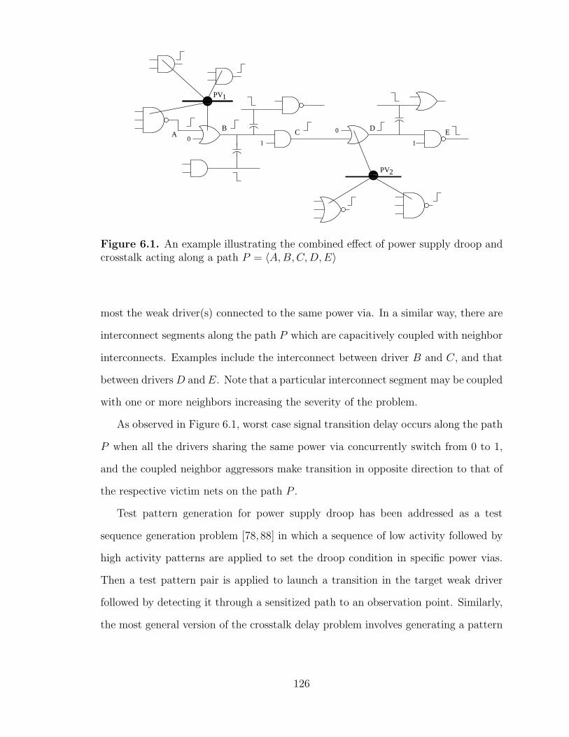
B
PV
PV
A C
1
2
1
0 D
1
E0
������������
������������
������
������
Figure 6.1. An example illustrating the combined effect of power supply droop andcrosstalk acting along a path P = 〈A,B,C,D,E〉
most the weak driver(s) connected to the same power via. In a similar way, there are
interconnect segments along the path P which are capacitively coupled with neighbor
interconnects. Examples include the interconnect between driver B and C, and that
between driversD and E. Note that a particular interconnect segment may be coupled
with one or more neighbors increasing the severity of the problem.
As observed in Figure 6.1, worst case signal transition delay occurs along the path
P when all the drivers sharing the same power via concurrently switch from 0 to 1,
and the coupled neighbor aggressors make transition in opposite direction to that of
the respective victim nets on the path P .
Test pattern generation for power supply droop has been addressed as a test
sequence generation problem [78, 88] in which a sequence of low activity followed by
high activity patterns are applied to set the droop condition in specific power vias.
Then a test pattern pair is applied to launch a transition in the target weak driver
followed by detecting it through a sensitized path to an observation point. Similarly,
the most general version of the crosstalk delay problem involves generating a pattern
126

pair that tests a transition delay fault along a “long” (i.e., low slack) path that
contains multiple victim nets, each possibly coupled with multiple aggressors [36].
It would be interesting to explore the formulation of an optimization problem
searching for a pattern pair 〈T1, T2〉 that would cause worst case delay along a specific
path through both 〈i〉 a set of droop-affected weak driver gates, and 〈ii〉 multiple vic-
tim nets capacitively coupled with aggressors. Clearly, this test pattern pair 〈T1, T2〉
has to be preceded with an input sequence that will set the droop condition in specific
power vias.
127
BIBLIOGRAPHY
[1] Dell poweredge processor:. http://www.dell.com/.
[2] Synopsys hspice user manual.http://www.synopsys.com/community/interoperability/pages/hspice.aspx.
[3] Abc: A system for sequential synthesis and verification. Berkeley Logic Syn-thesis and Verification Group, http://www.eecs.berkeley.edu/ alanmi/abc/.
[4] Abramovici, M., Breuer, M. A., and Friedman, A. D. In Digital Systems Testingand Testable Design (Piscataway, NJ 08855, 1995), IEEE Press.
[5] Agrawal, V. D., Kime, C. R., and Saluja, K. K. A tutorial on built-in self-test–part i: Principles. IEEE Design and Test of computers Vol. 10, No. 1 (1993),pp. 73–82.
[6] Bai, X., Dey, S., and Krstic, A. Hyac: A hybrid structural sat based atpg forcrosstalk. In Proceedings of the International Test Conference (2003), pp. 112–121.
[7] Bardell, P. H., McAnney, W. H., and Savir, J. In Built-in Test for VLSI:Pseudorandom techniques (New York, 1987), John Wiley and Sons.
[8] Barth, J.L., Dyer, C.S., and Stassinopoulos, E.G. Space, atmospheric, andterrestrial radiation environments. IEEE Trans. on Nuclear Science Vol. 50,No. 3 (2003), pp. 466–482.
[9] Baumann, R. C. Soft errors in advanced semiconductor devices-part i: the threeradiation sources. IEEE Trans. Device and Materials Reliability Vol. 1, No. 1(2001), pp. 17–22.
[10] Baumann, R. C. The impact of technology scaling on soft error rate performanceand limits to the efficacy of error correction. In Digest of International ElectronDevices Meeting (2002), pp. 329–332.
[11] Baumann, R. C. Ghosts in the machine: A tutorial on single-event upsets inadvanced commercial silicon technology. In Proceedings of International TestConference (2004).
[12] Baumann, R. C., Hossain, T. Z., Murata, S., and Kitagawa, H. Boron com-pounds as a dominant source of alpha particles in semiconductor devices. InProceedings of the International Reliability Physics Symposium (1995), pp. 297–302.
128
[13] Baze, M., and Buchner, S. Attenuation of single event induced pulses in cmoscombinational logic. IEEE Transactions on Nuclear Science Vol. 44, No. 6(1997), pp. 2217–2223.
[14] Bellido-Diaz, M. J., J.-Chico, J., Acosta, A. J., Valencia, M., and Huertas, J. L.Logical modeling of delay degradation effect in static cmos gates. IEEE Journalon Circuits, Devices and Systems Vol. 147, No. 2 (2000), pp. 107–117.
[15] Bryant, R. Cosmos: A complied simulator for mos circuits. In Proceedings ofthe IEEE/ACM Design Automation Conference (1987), pp. 9–16.
[16] Bushnell, M. L., and Agrawal, V. D. In Essentials of Electronic Testing ForDigital, Memeory & Mixed-Signal VLSI Circuits (Norwell, MA, 2000), KluwerAcademic Publishers.
[17] Cha, H., and Patel, J. H. A logic level model for α-particle hits in cmos circuits.In Proceedings of the International Conference on Computer Design (1993),pp. 538–542.
[18] Cha, H., Rudnick, E. M., Choi, G. S., Patel, J. H., and Iyer, R. K. A fast andaccurate gate-level transient fault simulation environment. In Proceedings of theInternational Symposium on Fault Tolerant Computing (1993), pp. 310–319.
[19] Chen, W. Y., Gupta, S. K., and Breuer, M. A. Test generation in vlsi circuitsfor crosstalk noise. In Proceedings of the International Test Conference (1998),pp. 641–650.
[20] Chen, W. Y., Gupta, S. K., and Breuer, M. A. Test generation for crosstalk-induced delay in integrated circuits. In Proceedings of the International TestConference (1999), pp. pp. 191–200.
[21] Cheng, Y.-K., and Kang, S.-M. A temperature-aware simulation environmentfor reliable ulsi chip design. IEEE Transactions on Computer Aided Design ofIntegrated Circuits and Systems Vol. 19, No. 10 (2000), pp. 1211–1220.
[22] Cheng, Y.-K., Raha, P., Teng, C. C., Rosenbaum, E., and Kang, S.-M. Illiads-t: An electrothermal simulator for thermal relaibility diagnosis of cmos vlsichips. IEEE Transactions on Computer Aided Design of Integrated Circuitsand Systems Vol. 17, No. 8 (1998), pp. 668–681.
[23] Cormen, T. H., Leiserson, C. E., and Rivest, R. L. In Introduction to Algorithms(1990), MIT Press.
[24] Cullen, C. G. In Linear Algebra with Applications (Reading, MA, 1997),Addison-Wesley.
[25] Czeck, E. W., and Siewiorek, D. P. Effects of transient gate level faults onprogram behavior. In Proceedings of the International Symposium on FaultTolerant Computing (1990), pp. 236–243.
129
[26] Devgan, A. Efficient coupled noise estimation for on-chip interconnects. InProceedings of the IEEE/ACM International Conference on Computer AidedDesign (1997), pp. 147–153.
[27] Devgan, A., and Nassif, S. Power variability and its impact on design. In Pro-ceedings of the IEEE International Conference on VLSI Design (2005), pp. pp.679–682.
[28] Dhillon, Y. S., Diril, A. U., and Chatterjee, A. Soft-error tolerance analysis andoptimization of nanometer circuits. In Proceedings of the Design, Automationand Test in Europe (2005), pp. 288–293.
[29] Diaz, C. H., Kang, S. M., and Duvvury, C. Circuit-level electrothermal sim-ulation of electrical overstress failures in advanced mos i/o protection devices.IEEE Transactions on Computer Aided Design of Integrated Circuits and Sys-tems Vol. 13, No. 4 (1994), pp. 482–493.
[30] Dodd, P. E., and Massengill, L. W. Basic mechanisms and modeling of single-event upset in digital microelectronics. IEEE Trans. Nuclear Science Vol. 50,No. 3 (2003), pp. 583–602.
[31] Encounter, SoC. In http://www.cadence.com/products/digital ic/soc encounter/index.aspx, Cadence Inc.
[32] Fortet, R. Applications de l’algebre de boole en recherche operationelle. RevueFrancaise de Recherche Operationelle Vol. 4 (1960), pp. 17–26.
[33] Fukahori, K., and Gray, P. R. Computer simulation of integrated circuits inthe presence of electrothermal interaction. IEEE Journal of Solid-State CircuitsVol. SC-11, No. 6 (1976), pp. 834–846.
[34] Ganeshpure, K., and Kundu, S. Automatic test pattern generation for maximalcircuit noise in multiple aggressor crosstalk faults. In Proceedings of the IEEEDesign, Automation, and Test in Europe Conference (2007), pp. pp. 540–545.
[35] Ganeshpure, K., and Kundu, S. On atpg for multiple aggressor crosstalk faultsin presence of gate delays. In Proceedings of the International Test Conference(2007).
[36] Ganeshpure, K., and Kundu, S. An ilp based atpg technique for multiple ag-gressor crosstalk faults considering the effects of gate delays. In Proceedings ofthe International Conference on VLSI Design (2009).
[37] Garey, M. R., and Johnson, D. S. In Computers and Intractability: A Guide tothe Theory of NP-Completeness (New York, 1979), W. H. Freeman.
[38] Gault, J. W., Robinson, J. P., and Reddy, S. M. Multiple fault detection incombinational networks. IEEE Trans. Computers, Vol. C-21, No. 1 (1972), pp.31–36.
130
[39] Gill, B. S., Papachristou, C., Wolff, F. G., and Seifert, N. Node sensitivityanalysis for soft errors in cmos logic. In Proceedings of the IEEE InternationalTest Conference (2005), pp. 964–972.
[40] Gong, J., Pan, D. Z., and Srinivas, P. V. mproved crosstalk modeling for noiseconstrained interconnect optimization. In Proceedings of the IEEE Asia andSouth Pacific Design Automation Conference (2001), pp. pp. 373–378.
[41] Gossett, C. A., Hughlock, B. W., Katoozi, M., LaRue, G. S., and Wender,S. A. Single event phenomena in atmospheric neutron environments. IEEETrans. Nucl. Sci. Vol. 40 (1993), pp. 1845–1856.
[42] Hetherington, G., Fryars, T., Tamarapalli, N., Kassab, M., Hassan, A., andRajski, J. Logic bist for large industrial designs: Real issues and case studies.In Proceedings of the International Test Conference (1999), pp. pp. 358–367.
[43] Horowitz, M. A. Timing models for mos circuits. In Tech. Rep. SEL83-003(1983), Integrated Circuits Laboratory, Stanford University.
[44] Hrishikesh, M. S., Jouppi, N. P., and Farkas, K. I. The optimal logic depth perpipeline stage is 6 to 8 fo4 inverter delays. In Proceedings of the 29th AnnualInternational Symposium on Computer Architecture (2002), pp. pp. 14–24.
[45] Hsieh, C. M., Murley, P. C., and O’Brien, R. R. Dynamics of charge collectionfrom alpha-particle tracks in integrated circuits. In Proceedings of InternationalReliability Physics Symposium (1981), pp. 38–42.
[46] Hu, C., and et. al. Bsim4 gate leakage model including source-drain partition.In International Electron Device Meeting (2000), pp. pp. 815–818.
[47] Hu, C., and et al. Bsim4.5.0 mosfet model. In User’s Manual (2004).
[48] ITRS. Process integration, devices, and structures. International TechnologyRoadmap for Semiconductors.
[49] ITRS. In http://www.itrs.net/Common/2004Update/2004 03 PIDS.pdf (2004),International Technology Roadmap for Semiconductors.
[50] Iyengar, V. S., and Brand, D. Synthesis of pseudo-random pattern testabledesigns. In Proceedings of the International Test Conference (1989), pp. pp.501–508.
[51] Juhnke, T., and Klar, H. Calculation of the soft error rate of submicron cmoslogic circuits. Journal of Solid Sate Circuits Vol. 30, No. 7 (1999), pp. 830–834.
[52] Kahng, A. B., Muddu, S., and Vidhani, D. Noise and delay uncertainty stud-ies for coupled rc interconnects. In Proceedings of the IEEE InternationalASIC/SOC Conference (1999), pp. pp. 3–8.
131
[53] Karnik, T., and Hazucha, P.. Characterization of soft errors caused by singleevent upsets in cmos processes. IEEE Transactions on Dependable and SecureComputing Vol. 1, No. 2 (2004), pp. 128–143.
[54] Kawaguchi, H., and Sakurai, T. Delay and noise formulas for capacitivelycoupled distributed rc lines. In Proceedings of the IEEE Asia and South PacificDesign Automation Conference (1998), pp. pp. 35–43.
[55] Kit, GNU Linear Program. In http://www.gnu.org/software/glpk/.
[56] Klaasen, F. M. Mos devices modelling. In In Design of VLSI Circuits forCommunications (Upper Saddle River, NJ, 1995), Prentice Hall.
[57] Klaasen, F. M., and Hes, W. On the temperature co-efficient of mosfet thresholdvoltage. Solid State Electronics Vol. 29, No. 8, pp. 787–789.
[58] Kobayashi, H., Usuki, H., Shiraishi, K., Tsuchiya, H. Hiroo, Kawamoto, N.,Merchant, G., and Kase, J. Comparison between neutron-induced system-serand accelerated-ser in srams. In Proceedings of the International ReliabilityPhysics Symposium (2004), pp. 288–293.
[59] Kong, J., Pan, D. Z., and Srinivas, P. V. Improved crosstalk modeling for noiseconstrained interconnect optimization. In Proceedings of the Asia and SouthPacific Design Automation Conference (2001).
[60] Krishnaswamy, S., Markov, I. L., and Hayes, J. P. Testing logic circuits fortransient faults. In Proceedings of the IEEE European Test Symposium (2005),pp. 102–107.
[61] Krstic, A., Liou, J.-J, Jiang, Y.-M., and Cheng, K.-T. Delay testing consideringcrosstalk-induced effects. In Proceedings of the International Test Conference(2001), pp. pp. 558–567.
[62] Kundu, S., Sengupta, S., and Galivanche, R. Test challenges in nanometertechnologies. In Proceedings of the European Test Workshop (2000), pp. pp.83–90.
[63] Kundu, S., Zachariah, S. T., and Chang, Y.-S. On modeling crosstalk faults.IEEE Transactions on Computer Aided Design of Integrated Circuits and Sys-tems Vol. 24, No. 12 (2005), pp. 1909–1915.
[64] Kuppuswami, R., DesRosier, P., Feltham, D., Sheikh, R., and Thadikaran,P. Full hold-scan systems in microprocessors: Cost/benefit analysis. IntelTechnology Journal Vol. 08, No. 1 (2004), pp. 63–72.
[65] Kushida, K., Otsuka, N., Hirabayashi, O., and Takeyama, Y. Dft techniquesfor memory macro with built-in ecc. In Proceedings of the IEEE InternationalWorkshop on Memory Technology, Design, and Testing (2005).
132
[66] Larrabee, T. Test pattern generation using boolean satisfiability. IEEE Trans.Computer-Aided Design Vol. 11, No. 1 (1992), pp. 4–15.
[67] Lee, H. K., and Ha, D. S. Atalanta: an atpg tool. In Tech. Rep. 93-12 (Blacks-burg, VA, 1994), Bradley Dept. of Electrical Engineering, Virginia Polytechnicand State University.
[68] Lee, K.-J., and Skadron, K. Using performance counters for runtime tem-perature sensing in high-performance processors. In Proceedings of the IEEEInternational Parallel and Distributed Processing Symposium (2005).
[69] Lee, S.-S., and Allstot, D. J. Electrothermal simulation of integrated circuits.IEEE Journal of Solid-State Circuits Vol. 28, No. 12 (1993), pp. 1283–1293.
[70] Liden, P., Dahlgren, P., Johansson, P., and Karlsson, J. On latching probabilityof particle induced transients in combinational networks. In Proceedings of theInternational Symposium on Fault Tolerant Computing (1994), pp. 340–349.
[71] Liden, P., Dahlgren, P., Johansson, R., and Karlsson, J. On latching probabilityof particle induced transients in combinational networks. In Proceedings of theInternational Symposium on Fault Tolerant Computing (1994), pp. 340–349.
[72] Madge, R., Benware, B., Turakhia, R., Daasch, R., Schuermyer, C., and Ruffler,J. In search of the optimum test set – adaptive test methods for maximumdefect coverage and lowest test cost. In Proceedings of the International TestConference (2004), pp. pp. 203–212.
[73] Manich, S., and Figueras, J. Maximizing the weighted switching activity incombinational cmos circuits under the variable delay model. In Proceedings ofthe European Design and Test Conference (1997), pp. pp. 597–602.
[74] Matlab. In http://www.mathworks.com/products/matlab/, The MathWorks.
[75] May, T. C., and Woods, M. H. Alpha-particle-induced soft errors in dynamicmemories. IEEE Trans. Electron Devices Vol. ED-26 (1979), pp. 2–8.
[76] Meaney, P. J., Swaney, S. B., Sanda, P. N., and Spainhower, L. Ibm z990soft error detection and recovery. IEEE Transactions on Device and MaterialsReliability Vol. 5, No. 3 (2005), pp. 419–427.
[77] Mitra, D., Bhattacharjee, S., Sur-Kolay, S., Bhattacharya, B. B., Zachariah,S. T., and Kundu, S. Test pattern generation for power supply droop faults. InProceedings of the IEEE International Conference on VLSI Design (2006).
[78] Mitra, D., Bhattacharjee, S., Sur-Kolay, S., Bhattacharya, B. B., Zachariah,S. T., and Kundu, S. Test pattern generation for power supply droop faults. InProceedings of the International Conference on VLSI Design (2006).
133
[79] Mitra, S., Seifert, N., Zhang, M., Shi, Q., and Kim, K.S. Robust system designwith built-in soft-error resilience. IEEE Computer Vol. 38, No. 2 (2005), pp.43–52.
[80] Mohanram, K. Closed-form simulation and robustness models for seu-tolerantdesign. In Proceedings of the VLSI Test Symposium (2005), pp. 327–333.
[81] Mukherjee, S. S., Emer, J., and Reinhardt, S. K. The soft error problem: anarchitectural perspective. In Proceedings of the International Symposium onHigh-Perfornamce Computer Architecture (2005).
[82] Mukhopadhyay, S., Bhunia, S., and Roy, K. Modeling and analysis of loadingeffect in leakage of nano-scaled bulk-cmos logic circuits. In Proceedings of theIEEE Design, Automation, and Test in Europe Conference (2005), pp. pp. 224–229.
[83] Nakagawa, S., Sylvester, D. M., McBride, J., and Oh, S.-Y. On-chip crosstalknoise model for deep-submicrometer ulsi interconnect. Hewlett-Packard JournalVol. 49, No. (1998), pp. 39–45.
[84] Nguyen, H. T., , and Yagil, Y. A systematic approach to ser estimation andsolutions. In Proceedings of the Annual International Reliability Physics Sym-posium (2003), pp. 60–70.
[85] Oldham, T. R., Murrill, S., and Self, C. T. Single event upset of vlsi mem-ory circuits induced by thermal neutrons. Radiation Effects, Research, andEngineering Vol. 5, No. 1 (1986), pp. 4–12.
[86] Paul, B., and Roy, K. Testing crosstalk-induced delay faults in static cmoscircuits through dynamic timing analysis. In Proceedings of the InternationalTest Conference (2002), pp. pp. 384–390.
[87] Pecht, M. G., Radojic, R., and Rao, G. In Managing Silicon Chip Reliability(1998), CRC Press.
[88] Polian, I., Czutro, A., Kundu, S., and Becker, B. Power droop testing. IEEEDesign & Test of Computers (2007).
[89] Polian, I., Hayes, J. P., Kundu, S., and Becker, B. Transient fault characteri-zation in dynamic noisy environments. In Proceedings of the International TestConference (2005).
[90] PrimeTime. Primetime modeling user guide. Synopsys Inc. Vol. Z-2007.06-SP3 .
[91] Rabaey, J. M., Chandrakasan, A., and Nikolic, B. In Digital Integrated Circuits(New Jersy, 2003), Prentice Hall.
134

[92] Rao, R., Burns, J., Devgan, A., and Brown, R. Efficient techniques for gateleakage estimation. In Proceedings of the International Symposium on LowPower Electronic Design (2003), pp. pp. 100–103.
[93] Rastogi, A., Chen, W., and Kundu, S. On estimating impact of loading effecton leakage current in sub-65nm scaled cmos circuits based on newton-raphsonmethod. In Proceedings of the IEEE/ACM Design Automation Conference(2007), pp. pp. 712–715.
[94] Sakurai, T. Closed-form expressions for interconnection delay, coupling andcrosstalk in vlsis. IEEE Transactions on Electron Devices Vol. 40, No. 1 (1993),pp. 118–124.
[95] Sakurai, T., and Newton, A. R. Alpha-power law mosfet model and its appli-cations to cmos inverter delay and other formulas. IEEE Journal of Solid StateCircuits Vol. 25, No. 2 (1990), pp. 584–594.
[96] Sanyal, A., Alam, S. M., and Kundu, S. A built-in self-test scheme for soft errorrate characterization. In Proceedings of the IEEE International Online TestingSymposium (2008), pp. pp. 65–70.
[97] Sanyal, A., Alam, S. M., and Kundu, S. Built-in self-test for detection andcharacterization of transient and parametric failures. IEEE Design & Test ofComputers (2010), (Accepted).
[98] Sanyal, A., Ganeshpure, K., and Kundu, S. Accelerating soft error rate testingthrough pattern selection. In Proceedings of the IEEE International OnlineTesting Symposium (2007), pp. 191–193.
[99] Sanyal, A., Ganeshpure, K., and Kundu, S. On accelerating soft error detec-tion by targeted pattern generation. In Proceedings of the IEEE InternationalSymposium on Quality Electronic Design (2007), pp. 723–728.
[100] Sanyal, A., Ganeshpure, K., and Kundu, S. An improved soft-error rate mea-surement technique. IEEE Transactions on Computer Aided Design of Inte-grated Circuits and Systems Vol. 28, No. 4 (2009), pp. 596–600.
[101] Sanyal, A., and Kundu, S. On derating soft error probability based on strengthfiltering. In Proceedings of the IEEE International Online Testing Symposium(2007), pp. 152–157.
[102] Sanyal, A., and Kundu, S. A built-in test and characterization method forcircuit marginality related failures. In Proceedings of the IEEE InternationalSymposium on Quality Electronic Design (2008), pp. pp. 838–843.
[103] Sanyal, A., Pan, A., and Kundu, S. A study on impact of loading effect oncapacitive crosstalk noise. In Proceedings of the IEEE International Symposiumon Quality Electronic Design (2009).
135

[104] Sanyal, A., Rastogi, A., Chen, W., and Kundu, S. An efficient techniquefor leakage current estimation in nano-scaled cmos circuits incorporating self-loading effects. IEEE Transactions on Computers (2009), (Accepted).
[105] Seifert, N., Zhu, X., and Massengill, L. W. Impact of scaling on soft-error ratesin commercial microprocessors. IEEE Trans. On Nuclear Science Vol. 49, No.6 (2002), pp. 3100–3106.
[106] Shepard, K. L., and Narayanan, V. Noise in deep submicron digital design. InProceedings of the IEEE/ACM International Conference on Computer AidedDesign (1996), pp. pp. 524–531.
[107] Shivakumar, P., Kistler, M., Keckler, S. W., Burger, D., and Alvisi, L. Modelingthe effect of technology trends on the soft error rate of combinational logic. InProceedings of the International conf. Dependable Systems and Networks (2002),pp. 389–398.
[108] Skadron, K., and et al., M. Stan. Hotspot: Techniques for modeling ther-mal effects at the processor-architecture level. In Proceedings of the Interna-tional Workshop on Thermal Investigations of ICs and Systems (THERMINIC)(2002), pp. pp. 169–172.
[109] Srinivasan, G. R., Murley, P. C., and Tang, H. K. Accurate, predictive modelingof soft error rate due to cosmic rays and chip alpha radiation. In Proceedingsof the International Reliability Physics Symposium (1994).
[110] Srinivasan, V., Sternberg, A. L., Duncan, A. R., Robinson, W. H., Bhuva,B. L., and Massengil, L. W. Single-event mitigation in combinational logicusing targeted data path hardening. IEEE Transactions on Nuclear ScienceVol. 52, No. 6 (2005), pp. 2516–2523.
[111] Sutherland, I., Sproull, B., and Harris, D. In Logical effort: designing fastCMOS circuits (California, 1999), Morgan Caufmann.
[112] Tirumurti, C., Kundu, S., Sur-Kolay, S., and Chang, Y.-S. A modeling approachfor addressing power supply switching noise related failures of integrated cir-cuits. In Proceedings of the Design, Automation and Test in Europe (DATE)Conference (2004), pp. pp. 1078–1083.
[113] Tosaka, Y., Kanata, H., Satoh, S., and Itakura, T. Simple method for estimatingneutron-induced soft error rates based on modified bgr model. IEEE ElectronDevice Letters Vol. 20, No. 2 (1999).
[114] Tosaka, Y., Satoh, S., Itakura, T., Ehara, H., Ueda, T., Woffinden, G. A.,and Wender, S. A. Measurement and analysis of neutron-induced soft errorsin sub-half-micron cmos circuits. IEEE Trans. Electron Devices Vol. 45, No. 7(1998).
136
[115] Tsiatouhas, Y., Arapoyanni, A., Nikolos, D., and Haniotakis, T. A hierarchicalarchitecture for concurrent soft error detection based on current sensing. InProceedings of the IEEE International On-Line Testing Workshop (2002).
[116] Tsiatouhas, Y., Haniotakas, Th., Nikolos, D., and Efstathiou, C. Concurrentdectection of soft errors based on current monitoring. In Proceedings of theIEEE International On-Line Testing Workshop (2001), pp. pp. 106–110.
[117] Tsividis, Y. P. In Operation and modeling of the MOS Transistor (New York,1989), McGraw-Hill.
[118] Ulrich, E. G. Exclusive simulation of activity in digital networks. Communica-tions of the ACM Vol. 12, No. 2 (1969), pp. 102–110.
[119] Vargas, F., and Nicolaidis, M. Seu-tolerant sram design based on current mon-itoring. In Proceedings of the Fault Tolerant Computing Symposium (1994),pp. pp. 106–115.
[120] Vittal, A., Chen, L. H., Marek-Sadowska, M., Wang, K.-P., and Yang, S.Crosstalk in vlsi interconnections. IEEE Transactions on Computer-aided De-sign of Integrated Circuits and Systems Vol. 18, No. 12 (1999), pp. 1817–1824.
[121] Vittal, A., and Marek-Sadowska, M. Crosstalk reduction for vlsi. IEEE Trans-actions on Computer-aided Design of Integrated Circuits and Systems Vol. 16,No. 3 (1997), pp. 290–298.
[122] Wang, F., Xie, Y., Rajaraman, R., and Vaidyanathan, B. Soft error rate anal-ysis for combinational logic using an accurate electrical masking model. InProceedings of the International Conference on VLSI Design (2007), pp. 165–170.
[123] Wang, N. J., and Patel, S. J. Restore: Sympton-based soft error detection inmicroprocessors. IEEE Transactions on Dependable and Secure Computing Vol.3, No. 3 (2006), pp. 188–201.
[124] Wang, Z., Fang, H., Chakrabarty, K., and Bienek, M. Deviation-based lfsrreseeding for test-data compression. IEEE Transactions on Computer-AidedDesign of Integrated Circuits and Systems Vol. 28, No. 2 (2009), pp. 259–271.
[125] Weaver, C., Emer, J., Mukherjee, S. S., and Reinhardt, S. K. Techniques toreduce the soft error rate of a high-performance microprocessor. In Proceedingsof the International Symposium Computer Architecture (2004).
[126] Williams, T. W., and Daehn, W. Aliasing errors in multiple input signa-ture analysis registers. In Proceedings of the European Test Conference (1989),pp. pp. 338–345.
137
[127] Yilmaz, M., Hower, D. R., Ozev, S., and Sorin, D. J. Self-checking and self-diagnosing 32-bit microprocessor multiplier. In Proceedings of the InternationalTest Conference (2006), p. Paper 15.1.
[128] Zachariah, S. T., Chang, Y., Kundu, S., and Tirumurti, C. On modelingcrosstalk faults. In Proceedings of the Design, Automation and Test in EuropeConference (2003), pp. pp. 10490–10495.
[129] Zhang, B., Wang, W.-S., and Orshansky, M. Faser: Fast analysis of soft errorsusceptibility for cell-based designs. In Proceedings of the International Sympo-sium on Quality Electronic Design (2006).
[130] Zhang, M., and Shanbhag, N. R. A soft error rate analysis methodology. InProceedings of the International Conference on Computer Aided Design (2004),pp. 111–118.
[131] Ziegler, J. F., and Lanford, W. A. The effect of sea level cosmic rays on electronicdevices. I. Appl. Phys. Vol. 52 (1981), pp. 4305–4318.
138