on the properties and design of organic light-emitting devices
TRANSCRIPT

On the Properties and Design of
Organic Light-Emitting Devices
A DISSERTATION
SUBMITTED TO THE FACULTY OF THE GRADUATE SCHOOL
OF THE UNIVERSITY OF MINNESOTA
BY
Nicholas C. Erickson
IN PARTIAL FULFILLMENT OF THE REQUIREMENTS
FOR THE DEGREE OF
DOCTOR OF PHILOSOPHY
Russell J. Holmes, Advisor
January 2014

© Nicholas C. Erickson 2014

i
Acknowledgements
There are many people who contributed to this work and to my development as a
person and as a scientist. I must first thank my thesis advisor Prof. Russell J. Holmes.
Prof. Holmes’ support and dedication to our work inspired me to match his enthusiasm;
the culmination of our joint efforts is the presented herein. If I may call myself a scientist
at the end of this graduate career, it is because of his ability to not just lead, but develop,
young researchers. I will forever be shaped by my experience in the Holmes research
group.
Secondly, I acknowledge and thank my scientific collaborators: Dr. Daniele Braga
(UMN), Dr. Keun Hyung Lee (UMN), and Prof. C. Dan Frisbie (UMN) for the
preparation and discussion of organic thin film transistors and organic light-emitting
devices; Dr. Mike Manno (UMN) for his help in performing X-ray reflectivity
measurements necessary for understanding our exciton sensitization work; Dr. Sankar N.
Raman, Dr. John S. Hammond, and Dr. Scott Bryan from Physical Electronics for their
collaboration in measuring the composition depth profile of organic light-emitting
devices; and finally Prof. Jian Li (Arizona State University) for providing white-light
emitting compounds for use in single-layer, single-dopant white organic light-emitting
devices. I must also acknowledge the contributions made by the undergraduate and high
school researchers who I have had the joy of working with throughout my graduate
career: Luke Balhorn (UMN), Joe Loof (UMN), Robby Dorn (Breck), and Saeed
Hakimhashemi (Breck).
I thank the members of the Holmes research group, both past and present. I have
learned much from them, and their support and friendship over the years has made my
time at the University enjoyable. Finally, I thank my friends and family. My parents
have always supported my academic pursuits and their love and encouragement has made
me the person I am today. They have experienced every high and every low in this
journey with me, and this achievement is as much theirs as my own. I must also thank
my in-laws who have supported me and my family in this pursuit.
Lastly, I must thank my wife, Jenna. You inspire me to live up to the
opportunities I have had in life, and your love and support is the foundation on which all
my accomplishments stand.

ii
Dedication
To my wife, who sustains me.

iii
Abstract
Organic light-emitting devices (OLEDs) are attractive for use in next-generation
display and lighting technologies. In display applications, OLEDs offer a wide emission
color gamut, compatibility with flexible substrates, and high power efficiencies. In
lighting applications, OLEDs offer attractive features such as broadband emission, high-
performance, and potential compatibility with low-cost manufacturing methods. Despite
recent demonstrations of near unity internal quantum efficiencies (photons out per
electron in), OLED adoption lags conventional technologies, particularly in large-area
displays and general lighting applications.
This thesis seeks to understand the optical and electronic properties of OLED
materials and device architectures which lead to not only high peak efficiency, but also
reduced device complexity, high efficiency under high excitation, and optimal white-light
emission. This is accomplished through the careful manipulation of organic thin film
compositions fabricated via vacuum thermal evaporation, and the introduction of a novel
device architecture, the graded-emissive layer (G-EML). This device architecture offers
a unique platform to study the electronic properties of varying compositions of organic
semiconductors and the resulting device performance.
This thesis also introduces an experimental technique to measure the spatial
overlap of electrons and holes within an OLED’s emissive layer. This overlap is an
important parameter which is affected by the choice of materials and device design, and
greatly impacts the operation of the OLED at high excitation densities. Using the G-
EML device architecture, OLEDs with improved efficiency characteristics are
demonstrated, achieving simultaneously high brightness and high efficiency.

iv
Table of Contents
List of Tables ................................................................................................................. viii
List of Figures .................................................................................................................. ix
Chapter 1 – A Review of the Optical and Electronic Properties of Organic
Semiconducting Materials ............................................................................................... 1
1.1 What is an Organic Semiconductor? ........................................................................... 1
1.2 What is an Organic Thin Film? ................................................................................... 2
1.3 Character of the Excited State ..................................................................................... 3
1.3.1 Singlet and Triplet Excitons ......................................................................... 4
1.3.2 Electronic Transitions in Organic Semiconductors ..................................... 5
1.3.3 Fluorescence ................................................................................................ 8
1.3.4 Phosphorescence .......................................................................................... 9
1.4 Energy Transfer and Exciton Diffusion .................................................................... 11
1.4.1 Cascade Energy Transfer .......................................................................... 12
1.4.2 Förster Energy Transfer ............................................................................ 12
1.4.3 Dexter Energy Transfer ............................................................................. 14
1.4.4 Exciton Diffusion ....................................................................................... 15
1.5 Charge Transport in Organic Semiconductors .......................................................... 16
1.5.1 Band Transport .......................................................................................... 16
1.5.2 Hopping Transport .................................................................................... 17
Chapter 2 – Introduction to Organic Light-Emitting Devices ................................... 19
2.1 Thin Film and Device Fabrication ............................................................................ 19
2.1.1 Vacuum Thermal Evaporation ................................................................... 20
2.1.2 Formation of Cathode ................................................................................ 23
2.1.3 Complete OLED Fabrication Process ....................................................... 25
2.2 OLED Characterization and Data Analysis .............................................................. 25
2.2.1 Units of Optical Output in OLEDs ............................................................ 26
2.2.2 External Quantum Efficiency ..................................................................... 28
2.2.3 Power Efficiency ........................................................................................ 32
2.2.4 Measurement and Calculation of Device Parameters ............................... 33
2.3 Basic OLED Operation and Design .......................................................................... 36
2.3.1 The First OLED ......................................................................................... 36
2.3.2 The Use of an Emissive Guest .................................................................... 38
2.3.3 Achieving Broadband Emission ................................................................. 39
2.3.4 Multilayer OLED Operation ...................................................................... 39
2.3.5 Typical Device Operation .......................................................................... 41
2.3.6 Requirements for High-Efficiency OLEDs ................................................. 43
2.3.7 White-Light Emitting OLEDs ..................................................................... 44

v
2.3.8 State of the Art ........................................................................................... 46
2.4 Overview of this Thesis ............................................................................................ 46
Chapter 3 – Graded Composition Emissive Layer Light-Emitting Devices ............ 48
3.1 Evolution of OLED Architectures ........................................................................... 48
3.2 Graded-Composition Emissive Layer ....................................................................... 50
3.3 Optimization Red-G-EML OLEDs ........................................................................... 57
3.3.1 Red-Light Emitting G-EML OLEDs for Display Applications .................. 58
3.3.2 Red-Light Emitting G-EML OLEDs for Lighting Applications ................. 59
3.4 Optimizing Blue G-EML OLEDs ............................................................................. 61
3.4.1 Blue Light-Emitting Devices with TPBi as an ETL ................................... 62
3.4.2 Blue Light-Emitting Devices with 3TPYMB .............................................. 64
3.4.3 Multilayer FIrpic-Based OLEDs ............................................................... 65
3.5 Conclusion ................................................................................................................ 67
Chapter 4 – Depth Profiling of Organic Thin Films ................................................... 68
4.1 X-ray Photoelectron Spectroscopy ........................................................................... 70
4.2 Experimental Technique ........................................................................................... 70
4.3 XPS Study of Host Materials .................................................................................... 71
4.4 Depth Profiling of OLED Architectures ................................................................... 74
4.4.1 Resolution of the Unique Identification of TCTA and BPhen .................... 74
4.4.2 Characterization of the Mixed-Emissive Layer ......................................... 75
4.4.3 Characterization of the Graded-Emissive Layer ....................................... 78
4.5 Conclusion ................................................................................................................ 78
Chapter 5 – Electronic Properties of G-EML OLEDs ............................................... 80
5.1 Measurement of Charge Carrier Mobility ................................................................. 80
5.2 Single-Carrier Experimental Design ......................................................................... 81
5.3 Optimized Red- and Green-Emitting Devices .......................................................... 83
5.3.1 Performance of red- and green-emitting G-EML OLEDs ......................... 83
5.3.2 Charge Transport in Green and Red G-EML OLEDs ............................... 85
5.4 Optimized Blue-Light Emitting Devices .................................................................. 91
5.4.1 Performance of Blue Light-Emitting G-EML Devices ............................... 91
5.5 Flexible Transistor-Driven G-EML OLEDs ............................................................. 94
5.5.1 Organic Electrolyte-Gated Transistors ..................................................... 94
5.5.2 Transistor-Drive G-EML OLEDs .............................................................. 97
5.5.3 Dynamic Response of OET-Drive G-EML OLEDs .................................... 99
5.6 Conclusions ............................................................................................................. 102
Chapter 6 – Measurement of the Recombination Zone of Organic Light-Emitting
Devices ........................................................................................................................... 104

vi
6.1 Conventional Methods to Measure the Recombination Zone ................................. 106
6.2 Sensing Excitons with Energy Transfer .................................................................. 107
6.2.1 Theory of Exciton Sensitization ............................................................... 109
6.2.2 Theory of the Electronic Model of G-EML OLEDs ................................. 112
6.3 Experimental Methods ............................................................................................ 116
6.4 Measurements of the Exciton Recombination Zone ............................................... 117
6.5 Electronic Model of G-EML OLEDs ..................................................................... 123
6.6 Impact of Recombination Zone on Efficiency Roll-Off ......................................... 126
6.7 Conclusions and Acknowledgements ..................................................................... 127
Chapter 7 – Engineering Efficiency Roll-Off in Organic Light-
Emitting Devices ........................................................................................................... 129
7.1 Density-Driven Exciton Quenching Processes ....................................................... 130
7.2 Experimental Design ............................................................................................... 131
7.2.1 Device Architectures of Interest ............................................................... 131
7.2.2 Device Fabrication and Test Film Design ............................................... 133
7.3 Characterizing Triplet-Triplet Annihilation ............................................................ 134
7.4 Characterizing Triplet-Polaron Quenching ............................................................. 136
7.5 Predicting Efficiency Roll-Off in OLEDs .............................................................. 138
7.5.1 ηEQE Predictions for D-EML and G-EML Devices .................................. 138
7.5.2 Transient Electroluminescence of D-EML and G-EML Devices ............. 141
7.5.3 ηEQE Predictions for Large-Recombination Zone G-EML Devices ......... 143
7.6 Conclusions ............................................................................................................. 145
Chapter 8 – Optical Modeling of OLEDs .................................................................. 146
8.1 Theory of Optical Fields in OLEDs ........................................................................ 147
8.1.1 Transfer-Matrix Model of Optical Electric Fields ................................... 147
8.2 Optical Modeling Results for D-, M-, and G-EML OLEDs ................................... 151
8.2.1 Optical Electric Field Results .................................................................. 151
8.2.2 Predictions of Outcoupling Efficiency ..................................................... 151
8.3 Summary ................................................................................................................. 154
Chapter 9 – Single-Dopant, Single-Layer White Light-Emitting OLEDs .............. 156
9.1 Simultaneous Monomer and Excimer Emission ..................................................... 156
9.2 Pt-17 in Single-Layer G-EML Devices .................................................................. 157
9.2.1 G-EML Devices With Pt-17 ..................................................................... 158
9.2.2 G-EML Devices with 10 wt.% Pt-17 ........................................................ 160
9.2.3 Summary of Pt-17 Performance in G-EML Devices ................................ 161
9.3 Conclusions and Future Work ................................................................................ 163
vii
Chapter 10 – Future Research Directions ................................................................. 165
10.1 Summary of This Thesis ....................................................................................... 165
10.2 White OLEDs ........................................................................................................ 166
10.2.1 Simple, High-Quality White OLEDs ...................................................... 166
10.2.2 Engineering Broadband Emission ......................................................... 170
10.3 Understanding Device Operating Lifetimes ......................................................... 173
10.3.1 Understanding Device Operating Lifetimes .......................................... 173
10.3.2 Characterizing Degradation-Induced Exciton Quenching .................... 173
10.3.3 Characterizing Degradation-Induced Loss of Charge Balance ............ 174
10.4 Mitigating Efficiency Roll-Off ............................................................................. 175
10.4.1 Extraordinary Recombination Zone Widths .......................................... 175
10.4.2 Engineering Exciton Lifetime Through Device Design ......................... 176
Chapter 11 – Bibliography .......................................................................................... 178
Appendix ....................................................................................................................... 193
A: List of Publications, Presentations, and Patents ........................................................ 193
B: G-EML Electronic Simulation Code ......................................................................... 195
C: Optical Simulation Code ........................................................................................... 198
Optical Field Simulation .................................................................................... 198
Optical Emission and Outcoupling Simulation .................................................. 207
D: Copyright Notices ..................................................................................................... 216

viii
List of Tables
Table 5.1: Fit parameters for Ir(ppy)3-based single-carrier devices ............................... 88
Table 5.2: Fit parameters for PQIr-based single-carrier devices .................................... 88
Table 5.3: Fit parameters for FIrpic-based single-carrier devices .................................. 93
Table 6.1: ηEQE and roll-off parameters for D-, M-, and G-EML devices .................... 127
Table 7.1: Measured and best fit ηEQE roll-off parameters ........................................... 139

ix
List of Figures
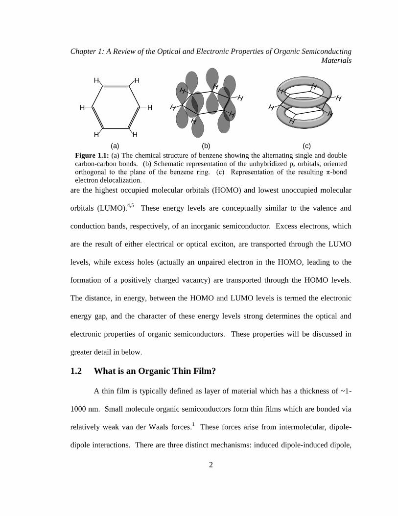
Figure 1.1: (a) The chemical structure of benzene showing the alternating single and
double carbon-carbon bonds. (b) Schematic representation of the unhybridized pz
orbitals, oriented orthogonal to the plane of the benzene ring. (c) Representation of the
resulting π-bond electron delocalization. ........................................................................... 2
Figure 1.2: Vector depiction of the four possible spin states of an electron-hole pair.
There are three permutations with the proper symmetry to give a net spin of S = 1, termed
“triplet” excitons, and one variation with anti-symmetry, which has a net spin of S = 0,
termed “singlet” excitons. .................................................................................................. 4
Figure 1.3: Energy level diagram of an organic semiconductor. S0 is the ground state,
while the first and second singlet and triplet excited states are S1 and S2, and T1 and T2,
respectively. The vibronic sub-level of each electronic level are indicated as 0, 1, 2. The
available electronic transitions for a molecule are: absorption, internal conversion,
fluorescence, intersystem crossing, and phosphorescence. ............................................... 6
Figure 1.4: (a) Energy level schematic depicting absorption transitions from the ground
state, S0,0 to higher-lying states, S1,n. After absorption, nuclear reorganization occurs and
emission transitions from S1,0 to vibronic levels in the ground state, S0,n may occur. (b)
The spectral shift in emission from absorption is the Franck-Condon shift. The intensity
of the absorption and emission transitions are determined by Fermi’s golden rule. ......... 8
Figure 1.5: Schematic diagram of the Förster energy transfer process. An exciton on the
donor molecule (D) sets up an oscillating electric field, which excites an electron on the
accepting molecule (A), resulting in an exciton on the acceptor and a donor molecule in
the ground state. ............................................................................................................... 13
Figure 1.6: (a) Schematic of hopping transport showing the energy barrier, EA, that must
be overcome in order transport charge. (b) The path of a carrier typically transports
through the lowest energy states available for conduction. ............................................. 17
Figure 2.1: Cross-sectional schematic of an OLED on a glass substrate. The anode is
typically pre-coated on the substrate. ............................................................................... 20
Figure 2.2: (a) Schematic of a typical vacuum thermal evaporation system. Organic
source powders are placed in the evaporation source boats, shown in (b) with common
dimensions (R.D. Mathis Co., evaporation source model: SB-6 (bottom) SB-6A (lid)).
Upon heating, the organic powders evaporate or sublime, leaving the source boat with a
Lambertian plume shape. ................................................................................................. 21
x
Figure 2.3: (a) Schematic of the cathode deposition through a shadow mask. (b) If the
mask is too thick, or the angle of the incoming Al vapor is large, edge effects may occur,
resulting in non-uniform electrodes. ................................................................................ 23
Figure 2.4: Photopic response of the standard human eye. The peak wavelength of
sensitivity is ~555nm. ...................................................................................................... 26
Figure 2.5: (a) Schematic of the forward hemisphere of light emission. All light which
escapes into this hemisphere escapes in the “forward viewing direction.” The angle θ is
defined from the normal to the source surface area, while φ is defined from the plane
which is parallel to the source surface area. (b) Schematic of the effective viewing
aperture for a surface source as a function of viewing angle θ. ....................................... 27
Figure 2.6: The outcoupling factor, ηOC, for an OLED results from the internal reflection
of some of the generated light. This is due to the index of refraction contrast between
the organic thin films, ITO, glass substrate, and air layers. ............................................. 30
Figure 2.7: Schematic of OLED testing setup for collection of JV and BV data. An
aperture prevents waveguide modes from contributing to measured output. .................. 34
Figure 2.8: Responsivity of the Hamamatsu S3584-08 silicon photodetector used in this
work. ................................................................................................................................ 35
Figure 2.9: (a) Diagram of the Tang and VanSlyke bilayer OLED. The organic layers
(TAPC, Alq3) are sandwiched by electrodes formed from ITO and Mg:Ag. (b) The
bilayer OLED diagram on an energy landscape, without the application of a voltage bias.
The HOMO and LUMO and work function values are taken from literature. ................ 37
Figure 2.10: (a) Energy diagram of prototypical three layer OLED at zero applied bias.
(b) Energy diagram of a device under bias, the exact degree of band bending is not well
characterized. The dilute-doped guest energy levels are represented by dashed lines. .. 40
Figure 2.11: Energy band diagram of an archetypical three-layer OLED with a
phosphorescent dopant, Ir(ppy)3. The chemical structures of the materials of interest are
also shown. ....................................................................................................................... 41
Figure 2.12 (a) Electroluminescent spectral output of the Ir(ppy)3-based device. (b)
Current density-voltage and brightness-voltage characteristics of the device of Figure
2.11. (c) calculated ηEQE and ηP. Peak values efficiencies are: ηEQE = 10.8% and ηP =
39.5 lm/W. ....................................................................................................................... 42
Figure 2.13: Efficiency progress and goals for solid-state OLED lighting. The US DOE
goal for both inorganic LED and OLED luminaires is 200lm/W by 2025. From the

xi
“Solid-State Lighting Research and Development Multi-Year Program Plan,” U.S.
DOE/EERE-0961 ............................................................................................................. 44
Figure 2.14: A white-light emitting tandem OLED. Copyright WILEY-VCH Verlag
GmbH & Co. KGaA, Weinheim, from Kanno et al. ........................................................ 46
Figure 3.1: Energy level diagram of a high-efficiency OLED. This device is comprised
of two transport layers, two charge/exciton blocking layers, and has an emissive layer
which contains two host materials in addition to an emissive guest. ............................... 49
Figure 3.2: (a) Schematic of a graded-composition layer. The HTM and ETM host
materials have a continuously-varying composition across the layer: from nearly 100% at
the respective electrode to 0% at the opposing electrode. The emissive guest
concentration is kept constant throughout the layer. (b) The deposition rate profiles of
the constituent materials. ................................................................................................. 50
Figure 3.3: (a) Energy levels of the green light-emitting G-EML device. Layer structure
of the simplified (b) double-emissive layer, and (c) mixed emissive layer devices. ....... 51
Figure 3.4: (a) Normalized EL spectra of M-EML, D-EML and G-EML OLEDs at a
brightness of 1000 cd/m2. (b) EL spectra of a G-EML OLED as a function of current
density. ............................................................................................................................. 53
Figure 3.5: Electroluminescence spectrum of a 1:1 TCTA:BPhen G-EML OLED without
any emissive guest. .......................................................................................................... 54
Figure 3.6: (a) Current density-voltage and (b) luminance-voltage characteristics for M-
EML (square), D-EML (circle), and G-EML (triangle) OLEDs. .................................... 55
Figure 3.7: External quantum (a) and power (b) efficiency versus current density for M-
EML (square), D-EML (circle), and G-EML (triangle) OLEDs. At 1000 cd/m2
the D-
EML OLED has ηEQE = 11.7% and ηP = 28.7 lm/W, while the G-EML OLED has ηEQE =
16.7% and ηP = 44.4 lm/W. .............................................................................................. 56
Figure 3.8: EL spectrum of PQIr in a G-EML OLED. The inset shows the chemical
structure together with the HOMO and LUMO energy levels, taken from literature. ..... 57
Figure 3.9: (a) Current density-voltage and brightness-voltage characteristics of PQIr-
based G-EML OLED. (b) ηEQE and ηP versus current density. Peak ηEQE = 12.7% and ηP
= 7.5 lm/W are achieved. ................................................................................................. 58
Figure 3.10: EL spectrum of PQIr in a G-EML OLED. The inset shows the chemical
structure. ........................................................................................................................... 59

xii
Figure 3.11: (a) Current density-voltage and brightness-voltage characteristics of
Ir(dpm)pq2-based G-EML OLED. (b) ηEQE and ηP versus current density. Peak ηEQE =
12.1% and ηP = 23.0 lm/W are achieved. ........................................................................ 60
Figure 3.12: (a) Deposition process for a 1:2 G-EML OLED, the growth rate of the
dopant is multiplied by a factor of 10 for visibility. (b) the resulting composition profile
of the device in (a). .......................................................................................................... 61
Figure 3.13: Electroluminescent spectrum of FIrpic, the energy levels and molecular
structure are inset. ............................................................................................................ 62
Figure 3.14: (a) Peak ηEQE of varying composition profile of FIrpic-based G-EML
devices. TCTA is used as an HTM with TPBi as an ETM. The molecular structure of
TPBi is shown in the inset. (b) The turn-on voltage (voltage at 1 cd/m2) and the voltage
required to produce 1000 cd/m2 as a function overall TPBi concentration. ................... 63
Figure 3.15: (a) Current density-voltage characteristics of the TCTA:3TPYMB-based
FIrpic G-EML devices. The molecular structure and energy levels of 3TPYMB are
shown in the inset. (b) The ηEQE of the three gradient profiles versus current-density.
The 1:2 gradient profile shows the highest peak ηEQE = 16.1%. ...................................... 65
Figure 3.16: (a) Current density-voltage and brightness-voltage characteristics of the
multilayer PNNL OLED. (b) Electroluminescent spectral output of the multilayer PNNL
OLED, with the molecular structures of PO15 and TAPC inset. .................................... 66
Figure 3.17: The ηEQE and ηP of the PNNL FIrpic-based OLED are shown versus current
density. ............................................................................................................................. 66
Figure 4.1: XPS spectra of the N 1s and C 1s of (a) TCTA and (b) BPhen. The N 1s
peaks are shifted, relative to each other, by 1.8 eV. ........................................................ 72
Figure 4.2: Full XPS spectra of a 100-nm-thick layer of BPhen on ITO. ..................... 73
Figure 4.3: Sputter depth profile of a TCTA (10 nm) / BPhen (100 nm) / TCTA (100nm)
/ ITO / glass stack. Signal from the Si substrate and from the TCTA N 1s peak is not
observed during the majority of the depth profiling of the BPhen layer. ........................ 74
Figure 4.4: Depth profile of a BPhen / TCTA D-EML structure. ................................. 75
Figure 4.5: XPS spectra for (a) C 1s and (b) N 1s peaks for a M-EML device on an ITO
substrate. The complete depth profile of the device is shown in (c). .............................. 76

xiii
Figure 4.6: Composition depth profiles of (a) 1:1, (b) 1:2, (c) and 1:3 gradient profiles
of TCTA:BPhen. The predicted gradient profiles for BPhen (squares) and TCTA
(circles) are shown overlaid on the depth profile data. .................................................... 77
Figure 5.1: Schematic of (a) electron-only and (b) hole-only device operation. ............ 82
Figure 5.2: Electroluminescence spectra at a brightness of 1000 cd/m2 for optimized G-
EML devices containing (a) 1:1 TCTA:BPhen with 2 wt.% Ir(ppy)3, (b) 1:1
TCTA:BPhen with 7 wt.% PQIr, and (c) 1:2 TCTA:TPBi with 4 wt.% FIrpic. Also shown
is the dependence of ηEQE and ηP on current density for the same optimized G-EML
structures containing (d) Ir(ppy)3, (e) PQIr, and (f) FIrpic. Vertical lines indicate
operation at a brightness of 1000 cd/m2. .......................................................................... 83
Figure 5.3: (a) Current density-voltage and (b) brightness-voltage characteristics for the
G-EML devices of Fig. 2. ................................................................................................ 84
Figure 5.4: External quantum efficiency versus current density for each of the gradient
profiles doped with either (a) 2 wt.% Ir(ppy)3 or (b) 7 wt.% PQIr. ................................. 85
Figure 5.5: Current density-voltage characteristics for 100:0 TCTA:BPhen (squares),
50:50 TCTA:BPhen (diamonds), and 0:100 TCTA:BPhen (triangles) electron-only, (a)
and (b), and hole-only, (c) and (d), single-carrier devices. Data for devices with 7 wt. %
Ir(ppy)3 are shown in (a) and (c), while data for devices with 2 wt. % PQIr are shown in
(b) and (d). Symbols are experimental data while solid lines are fits to Eqs. 5.1 and 5.2.
........................................................................................................................................... 86
Figure 5.6: Electron (solid symbols) and hole (open symbols) mobility for mixed films
as a function of the TCTA:BPhen composition ratio with (a) 2 wt. % Ir(ppy)3 at a field of
0.37 MV/cm and (b) 7 wt. % PQIr at a field of 0.44 MV/cm. The solid lines are guides to
the eye. ............................................................................................................................. 89
Figure 5.7: External quantum efficiency versus current density for FIrpic-based G-EML
devices with varying overall HTM:ETM composition. ................................................... 91
Figure 5.8: Current density-voltage characteristics for 100:0 TCTA:TPBi (squares),
50:50 TCTA:TPBi (diamonds), and 0:100 TCTA:TPBi (triangles) (a) electron-only and
(b) hole-only single-carrier devices with 4 wt.% FIrpic. Symbols represent measured
data while solid lines are fits to Eqns. 5.1 and 5.2. .......................................................... 92
Figure 5.9: Electron (solid symbols) and hole (open symbols) mobility at a field F = 0.30
MV/cm for mixed as a function of the TCTA:TPBi composition ratio with 4 wt. %
FIrpic. The solid lines are guides to the eye. .................................................................. 93
xiv
Figure 5.10: (a) Cross section of a printed organic thin film electrochemical transistor
(OET). When a negative gate voltage is applied, the semiconductor is electrochemically
doped by anions from the electrolyte and a high conductance state is created in the
transistor active layer. (b) Molecular structure of the employed electrolyte-dielectric and
(c) semiconductor (P3HT). The ion-gel dielectric is a solid electronic insulator made by a
gelating triblock copolymer (PS-PMMA-PS) swollen with an ionic liquid
([EMIM][TFSI]). ............................................................................................................. 95
Figure 5.11: Quasi-equilibrium transfer characteristics of a gel-electrolyte gated organic
transistor in linear (VD = -0.1 V) and saturation (VD = -1.5 V) regimes (sweep rate = 50
mV/s). Transistor channel length (L) and width (W) are L = 10 μm and W = 100 μm,
respectively. ..................................................................................................................... 96
Figure 5.12: Optical and electrical characteristics of an OET/OLED integrated device
using a green G-EML OLED. (a) Circuit diagram showing the driver TFT in series with
the light-emitting unit. (b) Luminance vs. supply voltage (VDD) at different gate voltages
(VGATE) and (c) luminance vs. gate voltage at different VDD. (d) Current density at the
OLED cathode versus VGATE for different VDD . Transistor channel length and channel
width are L = 20 μm and W = 200 μm, respectively. In the inset of Figure 3 (b) pictures
of the light-emitting unit at different brightness are also reported. ................................. 98
Figure 5.13: Optical response of an OET/OLED integrated device under dynamic
operation. (a) Luminance and driving TFT gate voltage vs. time at 10 Hz and (b)
luminance and TFT gate voltage vs. time at 100 Hz. In both cases the constant supply
voltage is VDD = -4.2 V. (c) Gate stress measurement on an integrated device at switching
frequency of 10 Hz and at a constant supply voltage VDD = -4 V. The upper and the
lower panels report the applied gate voltage and the device optical output versus time,
respectively. ................................................................................................................... 100
Figure 6.1: Layer structures for the (a) double- (D-EML), (b) mixed- (M-EML), and (c)
graded-emissive layer (G-EML) OLED architectures. The spatial composition profile
(wt. %) of the G-EML device is shown in (d). .............................................................. 108
Figure 6.2: (a) Extinction coefficient for the sensitizer, TPTBP, (dashed line) and peak-
normalized electroluminescence (EL) spectrum of the emissive guest, Ir(ppy)3 (solid
line). Inset: Molecular structure of TPTBP. (b) Schematic representation of the
sensitizing strip technique. ............................................................................................. 111
Figure 6.3: Current density-voltage characteristics (J-V) for (a) D-EML, (b) M-EML,
and (c) G-EML devices with a sensitizing strip located at different positions within the
emissive layer (as measured from anode, in the case of the D-EML and G-EML, or from
the TCTA/M-EML interface, for M-EML devices). Data for devices with intermediate
strip positions are omitted for clarity. A control device which does not contain the
sensitizing strip is shown (closed symbols) for each of the device architectures of interest.

xv
The current density at an applied voltage of 5 V for each device is shown in (d) for D-
EML devices, (e) for M-EML devices, and (f) for G-EML devices; the horizontal line
represents the average current density of the devices and error bars are calculated from
the current density variation of control devices fabricated in different runs. ................ 118
Figure 6.4: The relative exciton density versus position in (a) D-EML, (b) M-EML, and
(c) G-EML devices, at an applied current density of 10 mA cm-2
. For the D-EML device,
the recombination zone is centered at the TCTA/BPhen interface and has a spatial extent
of ~15 nm. In the case of the M-EML device, the spatial extent of the recombination
zone approaches ~40 nm and is centered on the TCTA side of the emissive layer. The
G-EML shows the largest recombination zone, with a spatial extent >80 nm, and is
centered in the middle of the device. ............................................................................. 120
Figure 6.5: Functions chosen to describe the spatial variation electron and hole
mobilities of a G-EML device. (b) Calculated electron and hole densities; both carrier
densities vanish at the opposing electrode, reflecting the boundary conditions and
situation where there is no leakage current. (c) The product N[X] × P[X] (NP product) is
plotted along with the measured recombination zone data of Figure 4. The NP product
has been scaled vertically, as the injected current density is arbitrarily set via the
boundary condition in Eqn. 6.18. ................................................................................... 122
Figure 6.6: Spatial variation of electron and hole mobilities for G-EML devices where
the ratio of electron to hole mobility is: μR = 0.01and μR = 0.1. (b) Spatial variation of
electron and hole mobilities for G-EML devices where μR = 10 and μR = 100. The
calculated N[X] and P[X] for the mobilities shown in (a) and (b) are shown in (c) and (d),
respectively. The resulting NP product of the carrier densities of (c) are shown in (e),
while the NP product for the carrier densities of (d) are shown in (f). .......................... 124
Figure 6.7: Peak-normalized ηEQE for D-EML, M-EML, and G-EML OLEDs. The J0
for each device is: 160 mA cm-2
, 375 mA cm
-2, and 360 mA cm
-2, for D-EML, M-EML,
and G-EML, respectively. .............................................................................................. 127
Figure 7.1: Transient photoluminescence decays for (a) TCTA:Ir(ppy)3, (b)
BPhen:Ir(ppy)3 and (c) TCTA:BPhen:Ir(ppy)3 thin films at different initial exciton
densities. Fits to Eqn. 7.4 for each measurement are shown as solid lines. .................. 135
Figure 7.2: Steady-state photoluminescence of hole-only (a) D-EML and (b) G-EML
devices at varying polaron densities. Fits to Eqn. 7.5 are shown as solid lines for each
device. ............................................................................................................................ 137
Figure 7.3: (a) Current density-voltage, brightness-voltage and (b) normalized ηEQE for
the D-EML device. (c) Current density-voltage, brightness-voltage and (d) normalized
ηEQE for the G-EML device. Fits to Eqn. 6 of the ηEQE of each device are shown as solid

xvi
lines. The J0 of each device is noted, J0 = 170 mA/cm2 for the D-EML device, J0 = 325
mA/cm2 for the G-EML device. ..................................................................................... 139
Figure 7.4: Triplet polaron quenching for a D-EML device with a narrow spatial overlap
of charges and excitons. Data from three devices show no observable decrease in steady-
state luminescence with increasing injected polaron density. ....................................... 141
Figure 7.5: (a) Transient electroluminescence decays for D- EML (squares) and G-
EML (circles) devices for a voltage pulse of 250ns, with a peak voltage, V = 25V. Bi-
exponential fits to the transient decay of each device are shown as solid lines. (b)
Transient fit lifetimes, τ1 (open) and τ2 (closed) as a function of voltage for D-EML
(squares) and G-EML (circles). ..................................................................................... 143
Figure 7.5: (a) Normalized ηEQEs for G-EML devices with varying recombination zone
widths, as predicted from Eqn. 6. Measured data for the G-EML device used in the
present study is shown (circles) together with the best fit to Eqn. 6. (bold line). (b) The J0
of each predicted device is shown versus recombination zone width. .......................... 144
Figure 8.1: General representation of a multilayer optical structure having m layers.
Each layer has a thickness of dj and an angle of refraction, θj. The electric field in each
layer is represented by two components propagating in positive and negative direction
(normal to layer, E+
j and E-j, respectively). The impact on the electric field due to
propagation across interfaces is described by the matrix Ij,k and propagation through
layers is described by the matrix Lj. .............................................................................. 147
Figure 8.2: (a) Optical electric field of a D-EML device at λ = 520nm. The field peaks
in the TCTA:Ir(ppy)3 layer and decays rapidly in the BPhen:Ir(ppy)3 layer. (b) The full
optical electric field for the visible wavelengths at each thickness in the device. Dark
colors represent low intensity optical fields. The ITO thickness spans the 0-150 nm, the
TCTA:Ir(ppy)3 spans 150-190 nm, BPhen:Ir(ppy)3 spans 190-230 nm, and the Al cathode
spans the 230-330nm thicknesses. ................................................................................. 149
Figure 8.3: (a) optical electric field distributions for the D-EML OLED which has the
structure: ITO (150 nm) / TCTA:Ir(ppy)3 (5 wt. %, 40 nm) / BPhen:Ir(ppy)3 (5 wt.%, 40
nm) / LiF (1 nm) / Al (100 nm). (b) The optical electric field for M-EML OLEDs with
the structure: ITO (150 nm) / TCTA (20 nm) / TCTA:BPhen:Ir(ppy)3 [50:50] (5 wt.%, 60
nm) / BPhen (20 nm) / LiF (1 nm) / Al (100 nm). (c) The optical electric field for G-
EML OLEDs with the structure: ITO (150 nm) / TCTA:BPhen:Ir(ppy)3 1:1 gradient (2
wt.%, 100 nm) / LiF (1 nm) / Al (100 nm). All fields are shown for a wavelength λ = 520
nm. ................................................................................................................................. 152
Figure 8.4: Simulated ηOC for an M-EML device with the structure: glass / ITO (150 nm)
/ TCTA (20 nm) / TCTA:BPhen:Ir(ppy)3 [50:50] : 5 wt.% (60 nm) / BPhen (20nm) / Al

xvii
(100 nm). The simulated ηOC closely follows the optical field simulated in Figure 8.3b.
......................................................................................................................................... 153
Figure 8.5: Simulated outcoupling efficiency (ηOC) for the G-EML device architecture.
A peak ηOC = 23.0% is predicted at a distance of 30 nm from the anode. An average ηOC
= 17.2% is predicted. ..................................................................................................... 154
Figure 9.1: (a) Current density-voltage and brightness-voltage characteristics of a 2 wt.%
Pt-17 G-EML device, the EL spectra of the device is shown in (b). The spectra shows
decreasing contributions from the excimer emission with the current density increasing
from 1 to 10 mA/cm2. .................................................................................................... 158
Figure 9.2: ηEQE and ηP of the 2 wt.% Pt-17 G-EML OLED as a function of current
density. ........................................................................................................................... 159
Figure 9.3: (a) Current density-voltage and brightness-voltage characteristics of a 10
wt.% Pt-17 G-EML device, the EL spectra of the device is shown in (b). The spectra
shows decreasing contributions from the excimer emission with the current density
increasing from 1 to 10 mA/cm2. ................................................................................... 160
Figure 9.4: ηEQE and ηP of the 2 wt.% Pt-17 G-EML OLED as a function of current
density. ........................................................................................................................... 161
Figure 9.5: Color render index (CRI) and color coordinated temperature (CCT) versus
Pt-17 concentration (wt. %) in 1:2 TCTA:3TPYMB G-EML devices. ......................... 162
Figure 9.6: Peak ηEQE and ηP for varying PT-17 doping concentrations (wt. %). Best
performance is observed in the 10 wt.% device, with a corresponding CRI = 82 and CCT
= 4000 K. ....................................................................................................................... 163
Figure 10.1: Schematic of a multi-dopant, single-layer OLED with a 1:2 HTM:ETM
gradient profile. The position of the dopant, doping concentration, thickness of the doped
regions, and gradient profile might all be adjusted to give peak white light-emission
performance. .................................................................................................................. 167
Figure 10.2: ηEQE, ηP and EL spectrum for a set of multi-dopant, single-layer OLEDs
with dopant orders of: (a) green-blue-red, (b) blue-green-red, and (c) red-green-blue.
......................................................................................................................................... 169
Figure 10.3: (a) Normalized photoluminescence spectra for varying concentrations of the
polar emitter C545T, shown in the inset. (b) Peak wavelength and the wavelengths at
one-half of the maximum intensity as a function of concentration. .............................. 171

xviii
Figure 10.4: (a) Normalized photoluminescence spectra for varying concentrations of the
polar emitter C545T in TCTA in thin films. (b) Peak wavelength and the wavelengths at
one-half of the maximum intensity as a function of concentration. A peak wavelength
shift of ~70 nm is observed. ........................................................................................... 172
Figure 10.5: Normalized ηEQE for a conventional G-EML device (open circles) with a
predicted ηEQE for a device with τ = 1.62 × 10⁻⁷
s (solid line). ....................................... 177

Chapter 1: A Review of the Optical and Electronic Properties of Organic Semiconducting
Materials
1
Chapter 1 - A Review of the Optical and Electronic Properties of
Organic Semiconducting Materials
1.1 What is an Organic Semiconductor?
Organic materials are broadly classified as chemical compounds which contain
carbon.1 Virtually millions of compounds which fit this definition have been discovered.
Those which are used in optical, electronic, and optoelectronic devices, however,
typically show some semiconducting properties due to a chemical bonding scheme of
alternating single and double bonds, termed conjugation.1,2
These organic
semiconductors are further classified by molecular weight, those with ‘small’ molecular
weights, mw <1 kg/mol, and those with larger molecular weights, which are typically
polymers (chains of repeat molecular units). This work will focus on the use of small
molecule organic semiconductors which are typically capable of sublimation or
evaporation without degradation.
Conjugation in these molecules is the result of the hybridization of the carbon 2p
and 2s electronic orbitals. Three sp2 orbitals are formed with a single, unhybridized pz
orbital left over. This remaining pz orbital is oriented out of the plane and may overlap
with neighboring pz orbitals, forming a π-bond and resulting in a delocalization of the
electron cloud. The unhybridized pz orbitals of the simple molecule benzene, chemical
structure shown in Figure 1.1a, are shown in Figure 1.1b, with the resulting delocalized
π-bond shown in Figure 1.1c. The overlapping π-bonds in a conjugated molecule result
in the formation of an array of available molecular energy levels.3 Of most importance
Chapter 1: A Review of the Optical and Electronic Properties of Organic Semiconducting
Materials
2
are the highest occupied molecular orbitals (HOMO) and lowest unoccupied molecular
orbitals (LUMO).4,5
These energy levels are conceptually similar to the valence and
conduction bands, respectively, of an inorganic semiconductor. Excess electrons, which
are the result of either electrical or optical exciton, are transported through the LUMO
levels, while excess holes (actually an unpaired electron in the HOMO, leading to the
formation of a positively charged vacancy) are transported through the HOMO levels.
The distance, in energy, between the HOMO and LUMO levels is termed the electronic
energy gap, and the character of these energy levels strong determines the optical and
electronic properties of organic semiconductors. These properties will be discussed in
greater detail in below.
1.2 What is an Organic Thin Film?
A thin film is typically defined as layer of material which has a thickness of ~1-
1000 nm. Small molecule organic semiconductors form thin films which are bonded via
relatively weak van der Waals forces.1 These forces arise from intermolecular, dipole-
dipole interactions. There are three distinct mechanisms: induced dipole-induced dipole,
Figure 1.1: (a) The chemical structure of benzene showing the alternating single and double
carbon-carbon bonds. (b) Schematic representation of the unhybridized pz orbitals, oriented
orthogonal to the plane of the benzene ring. (c) Representation of the resulting π-bond
electron delocalization.
HH
H H
HH
(a) (b) (c)

Chapter 1: A Review of the Optical and Electronic Properties of Organic Semiconducting
Materials
3
permanent dipole-induced dipole, and permanent dipole-permanent dipole. The first
mechanism, termed the London dispersion force,6 is due to the instantaneous fluctuations
of the electron density surrounding a molecule, resulting in an instantaneous polarization.
The polarization of one molecule may induce an instantaneous polarization in a nearby
molecule, resulting in an overall attraction between the two molecules. In this way
molecules with no permanent dipole may form stable films. The permanent dipole-
induced dipole (Debye force) and the permanent dipole-permanent dipole (Keesom force)
mechanisms occur when one or more of the constituent molecules has a permanent
dipole, a not uncommon feature of some molecules. The net result of the weak bonding
in a thin film of organic material is that the electronic properties of a thin film are often
similar to those of a single molecule. Additionally, the weak intermolecular bonding
renders the typical organic thin films mechanically soft.7,8
1.3 Character of the Excited State
An important precursor to the emission of light from an organic thin film is the
formation of an excited state. The excited state, termed an ‘exciton,’ consists of an
electron in the LUMO which is bound via a Coulomb force to a hole in the HOMO.9 Due
to the low relative dielectric constant of organic semiconductors (εR ~ 3), the exciton is
highly localized and has a large binding energy, >100 meV.1 An exciton which is
confined to a single molecule is termed a “Frenkel” exciton, while an exciton which
spans adjacent molecules is referred to as a “charge-transfer” exciton.1,10,11
Excitons
which are yet larger in spatial extent (“Wannier-Mott” excitons) are not typically
encountered in organic semiconductors.12
The large exciton binding energy found in

Chapter 1: A Review of the Optical and Electronic Properties of Organic Semiconducting
Materials
4
organic semiconductors allows them to persist at room temperature for a period of time
(the exciton “lifetime,” τ), before deactivation through the emission of a photon (light),
the emission of phonons (heat), or the transfer of energy to another molecule (energy
transfer).13–17
The characteristics and behavior of this energy-carrying, charge-neutral
quasiparticle is a principal factor in determining the operation and performance of
OLEDs.
1.3.1 Singlet and Triplet Excitons
As Fermions, electrons and holes have associated spins of S = +/- ½. The four
possible combinations of electron and hole spin in an exciton are depicted as rotating
Figure 1.2: Vector depiction of the four possible spin states of an electron-hole pair. There
are three permutations with the proper symmetry to give a net spin of S = 1, termed “triplet”
excitons, and one variation with anti-symmetry, which has a net spin of S = 0, termed
“singlet” excitons.
Z Z Z Z
X
S = 1
Triplet
S = 0
Singlet

Chapter 1: A Review of the Optical and Electronic Properties of Organic Semiconducting
Materials
5
vectors in Figure 1.2.9 An exciton, therefore, may have a total spin of magnitude S = 0,
when the spin vectors are out of phase (the anti-symmetric state), or S = 1, when the spin
vectors are in phase (the symmetric state). The degeneracy of each total spin state gives
the exciton its name, the S = 0 state being a ‘singlet’ exciton of single degeneracy, the S
= 1 state being a ‘triplet’ exciton of triple degeneracy. Under electrical excitation,
electrons and holes with uncorrelated spins bind to form excitons, therefore all four
configurations of exciton spin are produced. Simple statistics show that a population of
excitons formed this way will be 75% triplets and 25% singlets.18,19
The available and
dominant electronic transitions of an exciton are greatly affected by its spin state, a
matter addressed in the following sections.
1.3.2 Electronic Transitions in Organic Semiconductors
The energy levels and electronic transitions of an organic semiconductor are
illustrated in Figure 1.3. The ground state is S0; higher-lying singlet excited states are
labeled S1, S2, etc. Similarly, T1 and T2 indicate higher-lying triplet excited states. Each
state consists of a manifold of vibronic states which are close in energy to the primary
state, denoted by a second subscript (S1,0 indicates the lowest level vibronic in the first
excited state).
The rate of transition (kobs) between initial (subscript i) and final (subscript f) state
can be given by Fermi’s Golden rule:9
|⟨ | | ⟩| , (1.1)
where P is the strength of a perturbation acting on an initial wavefunction (Ψi) and ρ is
the density of resonant states for the transition. The Born-Oppenheimer approximation

Chapter 1: A Review of the Optical and Electronic Properties of Organic Semiconducting
Materials
6
states that the motion of electrons in the molecular orbitals is more rapid than the
vibration of the nuclei. This allows the total wave function, Ψ, to be separated into an
electronic wave function, ϕ, and a nuclear wave function, χ.2 This assumption is
generally valid for organic molecules, where the mass of the nuclei is much greater than
that of the electrons in the outer orbitals. Effectively, this requires that electronic
transitions occur on a time scale which is much shorter than the reorganization of the
nucleus in response to the transition.
The rate of an optical transition between states may be written in a Fermi’s golden
rule notation as:9
⟨ | - | ⟩
⟨ | ⟩, (1.2)
Figure 1.3: Energy level diagram of an organic semiconductor. S0 is the ground state, while
the first and second singlet and triplet excited states are S1 and S2, and T1 and T2, respectively.
The vibronic sub-level of each electronic level are indicated as 0, 1, 2. The available
electronic transitions for a molecule are: absorption, internal conversion, fluorescence,
intersystem crossing, and phosphorescence.
Energy
S0 Vibronics
S1
S2
012
012
012
012
T1
012
T2
Absorption
Fluorescence
Phosphorescence
Internal Conversion
Intersystem Crossing

Chapter 1: A Review of the Optical and Electronic Properties of Organic Semiconducting
Materials
7
where the first term is due to a is a dipole-dipole interaction and ΔEif is the separation in
energy of the two states, and the second term is due to the overlap of the vibrational
(nuclear) wave functions, termed the Franck-Condon factor; this factor is discussed in
greater detail below.2,9
The dipole operator, Pd-d, is itself symmetric, meaning it cannot
mix states which do not share spin symmetry. This requires that an optical transition
between Ψi and Ψf must be a singlet-singlet or triplet-triplet transition. Generally,
molecules in the ground state have filled HOMO energy levels, requiring that the
constituent, paired electrons have opposite spins, i.e. the anti-symmetric state. Under
first-order approximations, optical transitions from an excited, anti-symmetric state
(singlet exciton) are allowed, while optical transitions from excited symmetric states
(triplet excitons) are not.9
A schematic of an optical transition is depicted in Figure 1.4, where the energy
levels of a ground state and first singlet excited state are depicted together with their
vibronic manifolds. In Figure 1.4a, a photon is absorbed by an electron in the ground
state and is promoted to the vibronic level of a higher singlet energy state. The strength
of the transition is determined by the overlap of the ground state level (S0,0) with each
vibronic level. The strength of the transition determines the “intensity” of absorption,
depicted in Figure 1.4b. Once in an excited singlet state, an electron with excess energy
(energy above the lowest vibronic energy level in the S1 state) rapidly cools to the lowest
energy singlet level, S1,0 (rate ~1012
s-1
),9 in a process termed internal conversion. This
process occurs with the emission of phonons as a means to dissipate the excess energy.
From the Born-Oppenheimer approximation, the electronic transitions may be assumed to
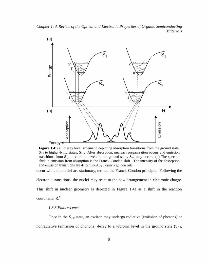
Chapter 1: A Review of the Optical and Electronic Properties of Organic Semiconducting
Materials
8
occur while the nuclei are stationary, termed the Franck-Condon principle. Following the
electronic transitions, the nuclei may react to the new arrangement in electronic charge.
This shift in nuclear geometry is depicted in Figure 1.4a as a shift in the reaction
coordinate, R.9
1.3.3 Fluorescence
Once in the S1,0 state, an exciton may undergo radiative (emission of photons) or
nonradiative (emission of phonons) decay to a vibronic level in the ground state (S0,1,
Figure 1.4: (a) Energy level schematic depicting absorption transitions from the ground state,
S0,0 to higher-lying states, S1,n. After absorption, nuclear reorganization occurs and emission
transitions from S1,0 to vibronic levels in the ground state, S0,n may occur. (b) The spectral
shift in emission from absorption is the Franck-Condon shift. The intensity of the absorption
and emission transitions are determined by Fermi’s golden rule
S0
0
1
2
S1
0’
1’
2’
S0
0
1
2
S1
0’
1’
2’
Energy
Em
issio
n
Ab
so
rptio
n
En
erg
y
(a)
(b) R

Chapter 1: A Review of the Optical and Electronic Properties of Organic Semiconducting
Materials
9
S0,2…). The emission of a photon during the transition of S1 S0 is called fluorescence.
The strength of the fluorescence transition, or intensity of emission, is determined by the
overlap of the S1,0 state and the vibronic energy levels of the ground state. The tendency
of electronic transitions to begin at the lowest vibronic energy level (S0,0 for absorption,
S1,0 for fluorescence) is known as Kasha’s Rule.20
Due to the nuclear reorientation
following the excitation of a molecule, the fluorescence of a molecule is shifted to lower
energy relative to absorption, termed the Franck-Condon shift.9 Absorption
spectroscopy, therefore, is an experimental technique which reveals the vibronic
character of the excited states in a molecule, while fluorescence spectra reflect the
vibronic character of the ground state. The efficiency with which fluorescence occurs,
ηfl, may be constructed as an equation of relative rates:
, (1.3)
where kR is the rate of radiative fluorescence decay, kNR is the rate of nonradiative decay,
and kT is the total radiative decay rate. The magnitude of ηfl may be quite high, indeed
experimental values which approach unity have been observed.21,22
Clearly, from Eqns.
1.1-1.3, the strength of the fluorescent transition, the overlap of the initial and final wave
functions, and any perturbations between the initial and final states are strong
determining factors in the ability of a molecular excited state to emit light.
1.3.4 Phosphorescence
A third process which may occur after the formation of an excited state (in
addition to fluorescence and nonradiative decay), is the transfer of that singlet excited
state energy to a triplet state (S1,0 T1,n), termed intersystem crossing.9 This process

Chapter 1: A Review of the Optical and Electronic Properties of Organic Semiconducting
Materials
10
requires one of the constituent electrons to “flip” its spin. In terms of Fermi’s golden
rule, the rate at which is the transition occurs (kISC) requires a mechanism to perturb the
spin state of an electron and is often very small, though non-zero. Once a triplet state has
been excited, both radiative and nonradiative decay pathways (to the ground state
vibronic manifold, S0,n) may be possible, the latter through the emission of phonons, the
former through the emission of photons. The process of photon emission from a triplet
state is termed phosphorescence. Again, the transition from T1,0 to S0,n requires a spin flip,
and therefore is seldom seen in typical organic semiconductors.
Given the small fraction of singlet excitons formed under electrical excitation
(~25%),18
there has been much effort aimed at harnessing triplet excitons in the process
of light emission. One way to achieve stronger emission from triplet excitons is to
introduce a perturbation to the electron spin states, effectively mixing the singlet and
triplet exciton spin states. One method has achieved this through the use of cyclometalic
organic molecules, which have heavy transition metal atom constituents.23
These
materials make use of the strong coupling of the electron spin angular momentum (S) and
the orbital angular moment of the electron (L), due to the relative motion of the nucleus
of the atom. This coupling is termed spin-orbit coupling, and its effect on the observable
rate of phosphorescence, kph, can be included in a Fermi’s golden rule rate equation (from
Eqn. 1.2):
⟨ | | ⟩
⟨ | ⟩
⟨ | | ⟩
(1.4)

Chapter 1: A Review of the Optical and Electronic Properties of Organic Semiconducting
Materials
11
where P’ is now a perturbation to the electronic wavefucntions, and Pso is the spin-orbit
coupling operator. The spin-orbit interaction of an electron in a hydrogen potential is
given by:2,9
, (1.5)
Where e is the elementary charge, ɛ0 is the permittivity of free space, m is the mass of the
electron, c is the speed of light, and r is the radius of motion. Ignoring the front factors, a
two-electron system will have a spin-orbit interaction:
, (1.6)
which becomes:
. (1.7)
The (S1+S2) operator is commutative with the total spin S, while (S1-S2) is not. It is this
second term which will give rise to a commutator of the electron spin states, i.e. it will
mix the singlet and triplet states. With strong spin-orbit coupling, kph may be enhanced
such that it competes with nonradiative decay pathways. The efficiency of
phosphorescence may be written similarly to ηfl,:
(1.8)
Experimental work has shown that with proper molecule design, ηph may approach
unity.24,25
1.4 Energy Transfer and Exciton Diffusion
While the previous sections have dealt with intramolecular excited state
transitions, there are several key intermolecular excited state transitions. These ‘energy

Chapter 1: A Review of the Optical and Electronic Properties of Organic Semiconducting
Materials
12
transfer’ processes transport the energy of an initial molecular exciton (the “donor”
molecule) to a second molecular exciton (the “acceptor” molecule). These processes
occur over a wide range of length scales and can be critical to OLED operation and
performance. There are three primary mechanisms which are responsible for energy
transfer: cascade energy transfer, Förster energy transfer, and Dexter energy transfer
1.4.1 Cascade Energy Transfer
Cascade energy transfer (or trivial energy transfer) is a mechanism which relies
on emission of a photon by the donor molecule and the subsequent absorption of that
photon by an acceptor molecule. The physical processes for this type of energy transfer
are readily explained in the context of the previous sections: an excited state radiatively
transitions to the ground state, some time later, a molecule absorbs the photon, and an
electron is promoted to a higher-lying singlet exciton state. The important parameters are
the efficiency of fluorescence (or phosphorescence) and the overlap of the emission
spectra with the acceptor absorption cross-section. The later takes into account both the
magnitude of the photon energy required and the strength of the absorption transition of
the acceptor molecule into various singlet excited state vibronics. This process may
occur over very large distances (10-100nm or more), provided the photon is allowed to
propagate in the intervening media.1,9
1.4.2 Förster Energy Transfer
Förster energy transfer (or Förster resonance energy transfer, FRET) is a
mechanism by which the energy of an exciton is transferred from a donor molecule to an
acceptor molecule via their overlapping dipole fields.1,9
This process may be

Chapter 1: A Review of the Optical and Electronic Properties of Organic Semiconducting
Materials
13
approximated as two interacting point dipoles and functions much like a simple
transmitting antenna-receiving antenna: an exciton in the donor produces an oscillating
electric field which drives the electrons of the acceptor in to resonance, shown in Figure
1.5. The energy of the exciton is fully transferred from donor to acceptor, which leaves
the donor in the ground state. This process may occur through occupied space; though,
as in the antenna analogy, the distance between the dipoles has a large effect on the
energy transfer process.
The rate of Förster energy transfer (kF) is given by:26
[ ]
(
)
, (1.9)
where τ is the exciton lifetime, d is the donor-acceptor molecular separation, and R0 is the
characteristic radius of Förster energy transfer, defined as the separation of the donor and
acceptor molecules where the rate of Förster energy transfer is equal to the rate of all the
other energy loss mechanisms. The Förster radius for a donor-acceptor pair is:9,26
∫ [ ] [ ] , (1.10)
where ηPL is the photoluminescence efficiency of the donor, κ is the dipole orientation
factor, n is the index of refraction of the medium between the donor and acceptor, λ is the
Figure 1.5: Schematic diagram of the Förster energy transfer process. An exciton on the
donor molecule (D) sets up an oscillating electric field, which excites an electron on the
accepting molecule (A), resulting in an exciton on the acceptor and a donor molecule in the
ground state.
HOMO
LUMOD A D DA A
D – Donor A - Acceptor

Chapter 1: A Review of the Optical and Electronic Properties of Organic Semiconducting
Materials
14
wavelength, FD is the area-normalized donor emission spectrum, and σA is the absorption
cross-section of the acceptor. Equation 1.10 can be viewed much like a Fermi’s golden
rule equation, the integral (weighted to include the strength of the acceptor’s absorption
transitions) is the overlapping density of states while the front factors determine the
magnitude of the transition operator. Like the Fermi’s golden rule equations describing
fluorescence, the initial and final states must have the same spin configuration, as the
dipole-dipole coupling transition does not include an operator which perturbs the spin
states. Thus, Förster energy transfer is typically restricted to singlet excitons, whose
fluorescence transitions do not require a spin flip. Given that a photon is a quantum of
the electromagnetic field, the coupling between the donor and acceptor molecule is often
described as the emission and absorption of a ‘virtual photon.’ The typical length scales
of Förster energy transfer are ~1-10 nm,1 though the properties of both the donor and
acceptor are important in determining the rate (and therefore efficiency) of energy
transfer.
1.4.3 Dexter Energy Transfer
Dexter energy transfer is process which physically transfers the excited state
electron from a donor molecule to an acceptor. This process is, therefore, a much
shorter-range energy transfer mechanism than the previously described processes. The
rate of Dexter energy transfer (kD) is:1,9
| |
∫ (1.11)
where h is Planck’s constant, βDA is the exchange energy interaction between molecules,
E is the energy, ED is the normalized donor emission spectrum, and AA is the normalized

Chapter 1: A Review of the Optical and Electronic Properties of Organic Semiconducting
Materials
15
acceptor spectrum. The dependence of Dexter energy transfer on donor-acceptor
separation can be included by assuming that the electron clouds of each molecule fall off
exponentially:9
⁄ ∫ . (1.12)
Here K is related to the specific orbital interactions, RDA is the donor-acceptor separation,
and R0 is defined as the separation at which the energy transfer process is equal to the
other rates of energy loss.
In comparison to Förster energy transfer, Dexter energy transfer also requires a
resonance of the density of states, represented by the integrals in Eqns. 1.11 and 1.12.
Also like Förster energy transfer, the process of the physical exchange of electrons
maintains the spin throughout the transfer. However, unlike Förster energy transfer, the
exchange process does not require mediation by a virtual photon , thus the exchange may
occur for excited states which do not have any wave function overlap with the ground
state. Dexter energy transfer is, therefore, the dominant mechanism by which triplet
excitons are transferred from donor to acceptor molecules.
1.4.4 Exciton Diffusion
The term exciton diffusion describes the net motion of exciton energy throughout
space. The diffusion process consists of multiple energy transfer events. Both Förster
and Dexter may contribute, though one process will typically dominate due to the spin
character of the exciton or the optical properties of either the donor or acceptor
molecules. In future chapters the impacts of exciton diffusion on OLED device design,
operation, and performance will be discussed.

Chapter 1: A Review of the Optical and Electronic Properties of Organic Semiconducting
Materials
16
1.5 Charge Transport in Organic Semiconductors
The topic of charge transport in organic semiconductors is an active area of
research.27,28
Typically, the nature of charge transport falls between two extremes: a
band transport model and a ‘hopping’ model. Band transport is most likely in materials
with long-range order, typically characteristic of crystalline thin films, where excess
electrons are greatly delocalized in space. A hopping model is more appropriate for
materials which are highly disordered, typically characteristic of materials where there is
little orientation of the molecules, i.e. amorphous thin films, where excess electrons in the
LUMO are highly localized in space.29
The balance of these transport regimes, and their
relevance to OLED device operation are discussed in the following sections.
1.5.1 Band Transport
The theory of band transport was initially developed to describe the electronic
properties of inorganic crystalline materials (now sometimes extended to crystalline
organic materials). It based on the premise that a long-range, periodic potential is formed
by the symmetry and order of an atomic (or molecular) lattice. The periodic potential
sets up an electronic wave function in the conduction band (or LUMO) that has a large
spatial extent, overlapping many lattice sites. The electron in a crystalline material is
able to travel rapidly through the conduction band in response to an applied electric field.
This is observed experimentally as a high mobility, μ = F/v, where v is the velocity of the
electron and F is the applied field. The temperature (T) dependence of the mobility in the
limit of band transport is:9
, (1.13)

Chapter 1: A Review of the Optical and Electronic Properties of Organic Semiconducting
Materials
17
where n > 1, and is a material dependent parameter. A signature of band transport,
therefore, is a decrease in mobility with increasing temperature. This is due to an
increase in the interactions of conduction-band electrons and phonons of the lattice.
1.5.2 Hopping Transport
Organic thin films, as discussed previously, are typically bonded via weak van der
Waals forces. This bonding scheme leads to very weak interactions between adjacent
molecules and results in a thin film which molecular orientations and spacings are highly
disordered. This disorder prevents the formation of a delocalized electronic band;
instead, carriers are confined to individual molecules. Due to the weak interaction
between molecules there is a barrier for electron transfer from one molecule to another.
Carrier conduction is thus an activated process, where an electron must overcome a
barrier in order to ‘hop’ to an adjacent site. Unlike the band transport limit, the carrier in
the hopping process spends enough time on each molecule to polarize the surrounding
lattice. The polarized lattice reconfigures to a new equilibrium state. Together, the
Figure 1.6: (a) Schematic of hopping transport showing the energy barrier, EA, that must be
overcome in order transport charge. (b) The path of a carrier typically transports through the
lowest energy states available for conduction.
En
erg
y
Position
EA
(a) (b)
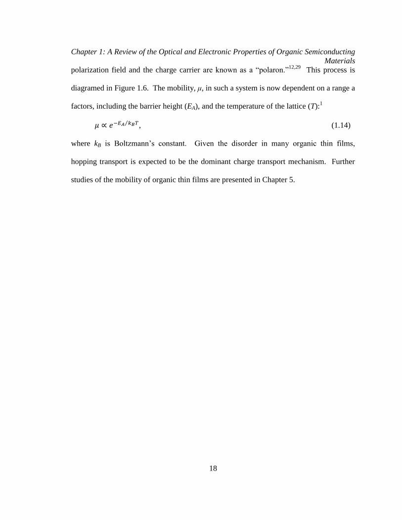
Chapter 1: A Review of the Optical and Electronic Properties of Organic Semiconducting
Materials
18
polarization field and the charge carrier are known as a “polaron.”12,29
This process is
diagramed in Figure 1.6. The mobility, μ, in such a system is now dependent on a range a
factors, including the barrier height (EA), and the temperature of the lattice (T):1
⁄ , (1.14)
where kB is Boltzmann’s constant. Given the disorder in many organic thin films,
hopping transport is expected to be the dominant charge transport mechanism. Further
studies of the mobility of organic thin films are presented in Chapter 5.

Chapter 2: Introduction to Organic Light-Emitting Devices
19
Chapter 2 - Introduction to Organic Light-Emitting Devices
2.1 Thin Film and Device Fabrication
There are several ways to achieve a thin film of a small molecule organic
semiconductor. Methods have been developed which are based on both liquid phase and
vapor phase processing,7,30,31
with powdered solids as the typical starting material.
Liquid phase processing requires soluble materials and appropriate solvents. Once in
solution, films may be formed by a variety of techniques, including: spin coating, ink-jet
printing, spray-coating, and doctor-blading. There is significant current interest in
developing materials which are compatible with the above techniques as they may
present paths to high-throughput, low-cost manufacturing on flexible substrates, such as
roll-to-roll processing.32,33
One current challenge in liquid phase processing is achieving
high performance multi-layered device structures, where each layer must be immune to
dissolution in subsequent liquid processing techniques.34,35
Vapor phase processing requires a method to transition the initial powdered
material from the solid to the gas phase. This is usually accomplished by heating the
material, either directly, with the use of a crucible or special boat, or through the use of a
hot carrier gas, as is the case in organic vapor phase deposition (OVPD).36,37
In OVPD,
the organic source material is heated in to the vapor phase, where it is transported, via the
hot carrier gas, through a heated reactor to a cooled substrate. This technique has many
benefits, such as high material utilization, high deposition rates, and compatibility with

Chapter 2: Introduction to Organic Light-Emitting Devices
20
roll-to-roll processing. However, film uniformity and control of mixed film composition
are still challenges.
2.1.1 Vacuum Thermal Evaporation
The most common method used to form the layers necessary for OLEDs (shown
schematically in Figure 2.1) is vacuum thermal evaporation (VTE).38
This
technique relies on heating the source powder in a crucible or folded metal source boat
(Tantalum or Tungsten are commonly used). An electrical current is passed through the
boat, causing resistive heating of the boat, which in turn heats the enclosed powder.
Under high-vacuum and applied heating, organic materials may evaporate from a melt, or
may sublime directly from the solid phase to the vapor phase. The deposition rate of the
VTE process is controlled by the heating of the boat. The opening of the boat behaves as
a surface source, with a vapor plume shape that has cosine dependence, similar to
Lambert’s cosine law. The substrates in such a system are placed a significant distance
from the source boat and are often on a rotation stage, to ensure uniform film thicknesses,
Figure 2.1: Cross-sectional schematic of an OLED on a glass substrate. The anode is
typically pre-coated on the substrate.
Glass
Anode
Organic Layers
(“device architecture”)
Cathode

Chapter 2: Introduction to Organic Light-Emitting Devices
21
the “throw distance” between the source boats and substrates is typically ~ 1 meter. A
schematic of a typical deposition system is shown in Figure 2.2a, a source boat is shown
in Figure 2.2b, with typical dimensions labeled.
Figure 2.2: (a) Schematic of a typical vacuum thermal evaporation system. Organic source
powders are placed in the evaporation source boats, shown in (b) with common dimensions
(R.D. Mathis Co., evaporation source model: SB-6 (bottom) SB-6A (lid)). Upon heating, the
organic powders evaporate or sublime, leaving the source boat with a Lambertian plume
shape.
Substrate
Evaporation
Sources
QCMs
PID
~10-7 Torr
Vacuum
Chamber
To Cryogenic
Pump
Shutter
(a)
(b)

Chapter 2: Introduction to Organic Light-Emitting Devices
22
Deposition rates in such a system are measured via quartz crystal microbalance
(QCM). Highly crystalline quartz undergoes a strong piezoelectric effect in response to
an applied voltage. Under an AC bias, a quartz crystal of a known thickness has a stable
frequency resonance; the resonant frequency shifts as the mass of the crystal is increased
via the deposition of organic molecules (or metal atoms) on the QCM surface. With a
simple assumption about the relationship of mass to film thickness, a rate of deposition
(thickness over time) is achieved.39,40
As the exact ratio of mass to thickness is difficult
to quantify for all materials of interest, a tooling factor is used. This factor is the ratio of
the actual, measured thickness to the desired thickness. With the use of an accurate
technique for deposition rate measurement and computer control of the power provided to
each deposition boat, an active feedback control loop may be established. With each loop
a computer, via a proportional-integral-derivative (PID) controller, is able to measure the
error between an intended rate and measured rate, and may adjust the applied power.
Changes in applied power will heat or cool the deposition boat, which will in turn adjust
the temperature, and deposition rate, of the target material. With accurate tooling factors
and PID settings, a target deposition rate which changes over time is attainable.
Deposition rates are typically on the order of ~1-4 Å/s with an experimental error of ±
0.04 Å/s.
Overall, this technique allows for very careful control of deposition rates, and thus
also film thickness and film composition. Multi-layered structures are trivial in such a
system, source boats are heated (and allowed to cool) in succession, allowing structures

Chapter 2: Introduction to Organic Light-Emitting Devices
23
with any number of layers to be fabricated. For these reasons, the VTE system is most
often used in settings where the utmost control over film mixing, thickness, etc. is
required. Devices reported in this thesis are exclusively fabricated via the VTE method.
2.1.2 Formation of Cathode
One important step in the production of an OLED is the fabrication of the top
metal electrode, typically the cathode of the device. The cathode is responsible for the
injection of electrons in to the device. Therefore, a metal with a low work function is
often desired to minimize the LUMO-work function energy difference. There are several
metals which are currently used, such as Al, Ag, and alloys of Mg:Ag.13,41
The most
common, however, is Al, due to its effectiveness, environmental stability, and low cost.
The Al deposition process is a high-vacuum thermal evaporation process, similar to the
deposition of organic materials. Al pellets (~4 mm in diameter) are placed in a tungsten-
wire basket. The basket is resistively heated, causing the Al pellets
Figure 2.3: (a) Schematic of the cathode deposition through a shadow mask. (b) If the mask
is too thick, or the angle of the incoming Al vapor is large, edge effects may occur, resulting in
non-uniform electrodes.
Substrate
Shadow Mask
Tungsten Wire Basket
High-Vacuum Chamber
Organic Layers
AlMask Mask
Incoming Al
(a) (b)

Chapter 2: Introduction to Organic Light-Emitting Devices
24
to melt and evaporate. To define the active area of OLED on a substrate, a shadow mask
is used to allow Al deposition to occur only in a specified area, shown schematically in
Figure 2.3a. It is important that the mask is very thin and flat, so that mask edge effects
and shadowing do not occur; an example of a mask edge effect is shown in Figure 2.3b.
One important, development in the performance of OLEDs is the use of an
interface-modifying layer at the organic/cathode interface. This layer is typically LiF,
and is deposited sequentially after the last organic layer and before the deposition of Al.
Effectively, the work function of the LiF/Al cathode is reduced for LiF thicknesses of ~1
nm. This greatly enhances electron injection into organic layers and has been shown to
enhance the performance of OLEDs.42,43
There are two ways in which LiF might reduce
the effective work function of the cathode. The first occurs with the dissociation of the
lithium and fluorine atoms by the incoming, energetic Al atoms. The free atoms may
then bond with either the organic molecules or Al atoms at the interface, resulting in a
smaller energy barrier between the Al and organic layers.44,45
A second route depends on
the large dipole moment measured for LiF thin films. It has been proposed that a thin
film of LiF would form a large interface dipole, enhancing the injection of electrons
through a reduction in the tunneling barrier.46
The latter mechanism would be highly
dependent on orientation of the LiF molecule and is considered unlikely. However,
measurements of the chemistry present at the organic-metal interface are difficult on thin
layers, particularly after Al deposition.47
Regardless of mechanism, the inclusion of LiF
in the formation of cathodes has become convention in OLEDs.

Chapter 2: Introduction to Organic Light-Emitting Devices
25
2.1.3 Complete OLED Fabrication Process
The fabrication of an OLED begins with a clean substrate. Dust, grease from the
manufacturing process, and oils from the skin all serve to reduce device operation and
yield. Substrate cleaning follows a standard procedure: sonication in a non-ionic
surfactant (Tergitol, Sigma Aldrich), sonication in deionized water, sonication in acetone,
and boiling in isopropyl alcohol. In this thesis, all OLEDs were fabricated on glass
substrates pre-coated with a 150-nm-thick layer of indium-tin oxide (ITO), a highly
transparent and conductive material, having a sheet resistance of 15 Ω/□. The ITO-
coated substrates were treated in UV-ozone ambient prior to loading in the VTE system.
All organic layers were grown using vacuum thermal sublimation (<10-7
Torr) without
breaking vacuum. Devices were defined by evaporating a cathode consisting of a 1-nm-
thick layer of LiF and a 100-nm-thick layer of Al through a shadow mask with 1 mm
diameter openings.
2.2 OLED Characterization and Data Analysis
Typical OLED operation and performance may be reported in the form of a few
figures of merit. These numbers may reflect the efficiency of luminescence, the optical
output of the device, the operating voltage of the device, as well as metrics which are
related to display or lighting applications. The sections below discuss these metrics, as
well as their use in understanding device operation, together with the experimental data
and equipment needed to achieve these metrics.

Chapter 2: Introduction to Organic Light-Emitting Devices
26
2.2.1 Units of Optical Output in OLEDs
The efficiency of an OLED is reported as optical output divided by electrical
input. A metric may be as simple as optical power out (WOPT) divided by input electrical
power (WOLED), referred to as the “wall-plug efficiency.” This efficiency, however, does
not reflect how well the device may operate as light source, intended for viewing with
human eyes. Indeed, the spectral sensitivity of the human eye (the “photopic” response,
Φ[λ]), in daylight conditions, has a narrow wavelength-response which is centered in the
green-yellow region of the visible spectrum (Figure 2.4).48
A useful characterization,
then, is to compare the emitted power spectrum of the OLED (or electroluminescence,
EL[λ]) to the photopic response of the human eye. This is done by calculating an average
wavelength of overlap factor, ϕ:
350 400 450 500 550 600 650 700 750 8000
100
200
300
400
500
600
700
Photo
pic
Response (
lm/W
)
Wavelength (nm)
Figure 2.4: Photopic response of the standard human eye. The peak wavelength of sensitivity
is ~555nm.

Chapter 2: Introduction to Organic Light-Emitting Devices
27
∫ [ ] [ ]
∫ [ ] . (2.1)
The units of ϕ are lumens (lm), which is an SI unit of luminous flux. Noting the output of
an OLED in terms of lumens is useful, as it automatically adjusts for emitted spectral
components that are not visible to the human eye. This is especially important for
OLEDs which are intended for display or lighting applications – the emission of
ultraviolet, or infra-red light is inherently a source of loss. Closely related to the lumen is
the candela (cd). This SI unit is defined as the power (in lumens) emitted by a source in
to a particular solid angle, and is a measure of brightness. For an OLED, the relevant
solid angle is the hemisphere directly above the substrate (Figure 2.5a), light which
escapes into this hemisphere is travelling into the “forward viewing direction,” and is
light which is useful for display and lighting applications. To calculate candelas, the
Figure 2.5: (a) Schematic of the forward hemisphere of light emission. All light which
escapes into this hemisphere escapes in the “forward viewing direction.” The angle θ is
defined from the normal to the source surface area, while φ is defined from the plane which is
parallel to the source surface area. (b) Schematic of the effective viewing aperture for a
surface source as a function of viewing angle θ.
θ
φ
Glass Substrate
OLED
Forward Viewing Direction
θ
l
θdl
(b)

Chapter 2: Introduction to Organic Light-Emitting Devices
28
luminous flux (in lumens) is integrated over the forward viewing hemisphere with the
important consideration that the OLED is not a point source, but is rather a surface
emitter. The power emitted versus viewing angle from a surface source follows
Lambert’s cosine law, which states that the brightness per solid angle, per unit area is
constant with changes in angle; as θ increases, the emission intensity decreases but the
solid angle decreases as well, this can be seen schematically in Figure 2.5b.
Conceptually, the surface area of the emitter can be thought of as an aperture through
which the luminous flux is observed. At off-normal angles, the intensity falls by a factor
of Cos[θ], but the effective aperture size (dl, in Figure 2.5b) falls by a factor of Sin[θ].
Experimentally, all output in the forward hemisphere is collected, so the conversion of
intensity in lumens to candelas, requires factoring in the Lambertian angular dependence
and the changing solid angle:
∫ ∫ [ ] [ ]
⁄
, (2.2)
where the angles θ and φ are defined in Figure 2.5a. The unit of candela is often
normalized to the surface area of the emitting device and is reported as cd/m2, this unit
has sometimes been referred to as a “nit.” Throughout this thesis, the luminescent output
of an OLED will be described units of cd/m2, and will be referred to as “brightness.”
2.2.2 External Quantum Efficiency
A fundamental of measure of the OLED efficiency is the external quantum
efficiency, or ηEQE. The ηEQE, as the name suggests, is the ratio of quantum output

Chapter 2: Introduction to Organic Light-Emitting Devices
29
(photons) to quantum input (electrons). The ηEQE metric only counts photons which
escape in to the forward viewing hemisphere. The conceptual definition for ηEQE is:13
, (2.3)
where χ is the spin fraction, γ is the charge balance factor, ηOC is the outcoupling
efficiency, and ηPL is the photoluminescence efficiency. The spin fraction, χ, of a device
is defined as the fraction of excitons which are allowed to decay radiatively. In the
language of Chapter 1, this is the fraction of excited states which have wave function
overlap with the ground state and do not require a spin flip (i.e. singlet excitons). For
typical fluorescent materials, χ = 0.25. However, from Chapter 1 section 3.4, strong spin-
orbit coupling allows for the radiative decay of triplet excited states; therefore, for
phosphorescent materials, χ = 1.0.
One recent development which challenges the above framework for χ, is the
demonstration of thermally activated delayed fluorescence (TADF).49,50
In this system, a
metal-free organic molecule is engineered so that the singlet and triplet energy levels
have a small energy gap (𝛥EST), such that the reverse intersystem crossing rate from
triplet to singlet, RISC, is enhanced. Despite the formation of triplet excitons under
electrical excitation, an enhanced RISC increases the probability that triplet excitons will
convert to singlets and undergo radiatively decay with an efficiency of ηFL. This leads to
an effective increase in χ, though the ratio of singlets to triplets formed is not impacted.
Molecules designed for TADF have recently been used to achieve high peak efficiency in
OLED.51

Chapter 2: Introduction to Organic Light-Emitting Devices
30
The charge balance factor, γ, is defined as the fraction of electrons injected into
the device which form excitons in the emissive region of the device. This parameter
quantifies loss mechanisms due to the charge which ‘leaks’ through the entire device
without forming excitons, and due to the formation of excitons outside of the intended
spatial region. The γ of a particular device is dependent on many aspects of the overall
device design and it is often used to assess the quality of device operation. For
particularly well designed OLEDs, γ may approach unity. The outcoupling factor, ηOC, is
the fraction of photons formed in the device which escape in to the far field in the
forward viewing direction. Due to the index of refraction contrast between the organic
layers, ITO, glass, and air, light generated in the active layers of the OLED may undergo
total internal reflection and be lost to horizontal wave guide or plasmon absorption
Figure 2.6: The outcoupling factor, ηOC, for an OLED results from the internal reflection of
some of the generated light. This is due to the index of refraction contrast between the
organic thin films, ITO, glass substrate, and air layers.
Cathode
Organic
Layers
ITO
Glass
Waveguide Modes
Forward Emitted

Chapter 2: Introduction to Organic Light-Emitting Devices
31
modes, shown in Figure 2.6. The exact calculation of the fraction of outcoupled light will
be addressed in Chapter 7, though a value of ηOC = 0.2 is often quoted. An initial guess
for nOC can be made using Snell’s law to calculate the critical angles for total internal
reflection for light transiting the ITO-glass and glass-air interfaces. Using the indices of
refraction for ITO, glass, and air (~2.2, 1.5, 1.0), the critical angle for the ITO-glass
interface is:
[
] .
Assuming that photons are emitted equally in all directions, the fraction of photons which
are not total internally reflected at this interface is ~ (43° × 2)/180° ≈ .48. Similarly, the
critical angle for total internal reflection at the glass-air interface is:
[
] .
Again, assuming that photons are approaching this interface at all angles, the fraction of
photons which are transmitted is ~ (42° × 2)/180° ≈ .47. Thus the total fraction of
photons which are transmitted across the ITO-glass and glass-air interfaces is = .48 × .47
≈ .22, or 22%. This maximum ηOC drastically reduces the maximum ηEQE achievable in a
standard OLED (where no attempt is made to enhance ηOC).
The final factor in eqn. 2.3 is the photoluminescence efficiency, ηPL. This factor
was addressed in the previous chapter for fluorescent (ηfl) and phosphorescent (ηph)
materials. Conceptually, it is defined as the fraction of excitons formed in the emissive
regions which undergo radiative decay, rather than nonradiative decay. With the proper
selection of emissive material, this factor may approach unity.24
All together, these four
Chapter 2: Introduction to Organic Light-Emitting Devices
32
factors conceptually define ηEQE. We can see from the maximum values of each of the
constituent parts (χ = 1.0, γ = 1.0, ηOC ≈ 0.2, ηPL ~1.0), ηEQE may approach a maximum of
0.20, or 20% for phosphorescent-based OLEDs. If we account for the typical optical loss
in an OLED due to ηOC, we may define an internal quantum efficiency, ηIQE = χ x γ x ηPL,
which represents the efficiency with which a particular device converts injected charge
carriers to generated photons.
2.2.3 Power Efficiency
While ηEQE may be a good metric of an OLED’s ability to convert charge to light,
it does not account for the power used by the OLED in the process, nor is it calibrated to
the response of the human eye. Therefore, it is beneficial to define a luminous power
efficiency, ηP, which is the ratio of optical power output (in lumens), per unit electron
power (W). This metric then has the units of lm/W and accounts for the spectral output
of the device relative to the photopic response, as well as the current injected into – and
the voltage used by – the OLED. This metric is defined in terms of the ηEQE as:
(2.4)
where ϕ is defined in Eqn. 2.1, Vphoton is the energy of the average photon emitted (in eV),
and VOLED is the voltage used by the device. The use of ηP implicitly assumes the use of
the OLED in display or lighting applications meant for observation by the human eye.
As it also accounts for the power used by the device, it is a definitive measure of display
and lighting OLED efficiency.
Chapter 2: Introduction to Organic Light-Emitting Devices
33
2.2.4 Measurement and Calculation of Device Parameters
The characterization of OLED operation and performance necessitates three main
measurements: the device current (IOLED, mA, often transformed to current density, J,
mA/cm2) versus voltage (VOLED, V), the brightness (B, cd/m
2) versus voltage, and the
spectral distribution of emitted light (EL[λ], W/cm2). Once collected, this data is
transformed and calibrated to produce the figures of merit and metrics used to
characterize OLEDs: the spectra (typically used as recorded, in W/cm2), the current
density-voltage characteristics (J-V plot), the brightness-voltage characteristics (B-V), and
the ηP and ηEQE of the device versus J, V, and/or B. The first plot is relatively straight
forward to achieve, a source-measurement unit with sufficient sensitivity (such as the
Agilent 4155C used throughout this thesis), and capable of sourcing and measuring both
current and voltage, is used to directly measure the current of the device at each applied
voltage. The EL spectrum of the device is measured via a fiber-coupled spectrometer (an
Ocean Optics HR4000 is used to cover a wavelength range of 300-900nm). A
measurement of brightness is achieved through the use of a large-area photodetector (a
Hamamatsu detector, model S3584-08 is used here). This detector is large enough such
that every photon emitted in the forward viewing direction is assumed to be collected.
An aperture is used to ensure that light which escapes through horizontal waveguide
modes is not collected (as it should not contribute to ηEQE), a schematic of this is shown
in Figure 2.7. The output of the photodiode, however, is not given in units of optical
power. Instead the detector outputs a current (Iph) which is proportional to the optical

Chapter 2: Introduction to Organic Light-Emitting Devices
34
power incident on the face of the detector. The proportionality constant is the
“responsivity” of the detector, in units of A/W. Each detector has a wavelength
dependent responsivity, R[λ], shown in Figure 2.8 for the detector used in this work.
Similar to the calculation of the spectral overlap with the average wavelength of photopic
response, the responsivity of the average wavelength is calculated:
∫ [ ] [ ]
∫ [ ] . (2.5)
From this, the actual optical power may be calculated by POPT = ⁄ at each
applied voltage. Using Eqns. 2.1 and 2.2, the luminance output (in lm) and B (in cd/m2)
may be calculated. With the luminance output calculated, ηP may now be computed at
each applied voltage (and current density). An alternative method of testing the optical
output of the device makes use of a spectroradiometer. This device is capable of
measuring the EL spectrum of the device and the total power output of the device
simultaneously. This measurement is often made at some distance from the substrate, so
an assumption of the angular distribution of the output is needed in order to properly
Figure 2.7: Schematic of OLED testing setup for collection of JV and BV data. An
aperture prevents waveguide modes from contributing to measured output.
OLED
Substrate
Aperture
Detector Face
Detector Body
Waveguide ModeCollected Emission

Chapter 2: Introduction to Organic Light-Emitting Devices
35
calculate output power.
A calculation of ηEQE is not made by measuring the parameters of Eqn. 2.3;
instead, the actual flux of photons emitted in to the forward viewing direction is
measured and compared to the flux of injected electrons. The latter part of this
measurement is made directly by the source measurement unit (the current of the device,
IOLED, being the number of charges per second, q/s). The flux of photons may be
calculated with POPT and a conversion from power to number of photons. This is done by
calculating the average wavelength of the spectral output:
∫ [ ]
∫
[ ]
. (2.6)
The photon flux is then, Pflux:
⁄
⁄, (2.7)
Figure 2.8: Responsivity of the Hamamatsu S3584-08 silicon photodetector used in this work.
200 400 600 800 1000 12000.0
0.1
0.2
0.3
0.4
0.5
0.6
0.7
Re
sp
onsiv
ity (
A/W
)
Wavelength (nm)

Chapter 2: Introduction to Organic Light-Emitting Devices
36
where h is Planck’s constant and c is the speed of light. A complete calculation of ηEQE
can now be written:
⁄
⁄
⁄
. (2.8)
2.3 Basic OLED Operation and Design
2.3.1 The First OLED
The first demonstration of electroluminescence (EL), that is luminescence based
on the injection of both electrons and holes from exterior contacts, was by Helfrich and
Schneider in 1965.52
They used a single crystal of anthracene with liquid metal contacts
formed from positive and negative ions of anthracene. The device required operating
voltages of ~102-10
4 V and achieved an efficiency of ~.1% (W/W). While this was an
important demonstration of EL in organic materials, the high voltages and low efficiency
of the device made it impractical for use in commercial applications. The revolutionary
report of efficient, low-voltage operation of an OLED came in 1987 from the Eastman
Kodak Company.53
Tang and VanSlyke, developed a bilayer structure formed from two
different organic semiconductors, a diamine, now known as di-[4-(N,N-ditolyl-amino)-
phenyl]cyclohexane (TAPC) and tris-(8-hydroxyquinoline)aluminum (Alq3).
Importantly, they were able to use ITO and a Mg:Ag alloy to attain efficient injection of
holes and electrons, respectively, into the organic layers (Figure 2.9a). They also
thermally evaporated both the organic active materials as well as the Mg:Ag cathode via
VTE, a much simpler method than previous demonstrations of organic EL which relied

Chapter 2: Introduction to Organic Light-Emitting Devices
37
on the use of single crystals. The ηEQE of the bilayer device reached a peak value of
~1.0% with a brightness as high as 103 cd/m
2 at voltages less than 10V. The operation of
the device is best described using an energy diagram of the structure, shown in Figure
2.9b. Upon application of an applied voltage, holes are injected from the ITO anode and
electrons are injected by the Mg:Ag cathode. Holes are transported by the electric field
across the TAPC, which serves as a hole transport layer (or HTL); similarly electrons are
transported across the Alq3, which is the electron transport layer (ETL). When both
carriers reach the interface one of three things may happen: a hole is injected on to the
HOMO of Alq3, an electron is injected on to the LUMO of TAPC, or an exciton is
formed across the two adjacent molecules, with the hole residing on the HOMO of the
TAPC, the electron on the LUMO of Alq3 (such an exciton is referred to as an
“exciplex”). Tang and VanSlyke observed only emission from the Alq3 species;
therefore it is likely that excitons were primarily formed on that species, according to the
Figure 2.9: (a) Diagram of the Tang and VanSlyke bilayer OLED. The organic layers
(TAPC, Alq3) are sandwiched by electrodes formed from ITO and Mg:Ag. (b) The bilayer
OLED diagram on an energy landscape, without the application of a voltage bias. The HOMO
and LUMO and work function values are taken from literature.
Glass
ITO
Diamine (TAPC)
Alq3
Mg:Ag
TAPC
~75nm
Alq3
~60nm
Mg:AgITO
2.0 eVHOMO
LUMO
En
erg
y5.5 eV
3.3 eV
6.0 eV
(a) (b)
4.7 eV
4.1 eV
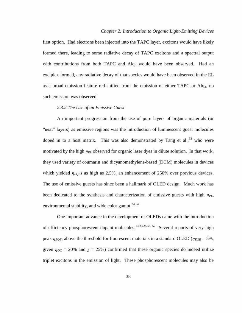
Chapter 2: Introduction to Organic Light-Emitting Devices
38
first option. Had electrons been injected into the TAPC layer, excitons would have likely
formed there, leading to some radiative decay of TAPC excitons and a spectral output
with contributions from both TAPC and Alq3 would have been observed. Had an
exciplex formed, any radiative decay of that species would have been observed in the EL
as a broad emission feature red-shifted from the emission of either TAPC or Alq3, no
such emission was observed.
2.3.2 The Use of an Emissive Guest
An important progression from the use of pure layers of organic materials (or
“neat” layers) as emissive regions was the introduction of luminescent guest molecules
doped in to a host matrix. This was also demonstrated by Tang et al.,53
who were
motivated by the high ηPL observed for organic laser dyes in dilute solution. In that work,
they used variety of coumarin and dicyanomethylene-based (DCM) molecules in devices
which yielded ηEQEs as high as 2.5%, an enhancement of 250% over previous devices.
The use of emissive guests has since been a hallmark of OLED design. Much work has
been dedicated to the synthesis and characterization of emissive guests with high ηPL,
environmental stability, and wide color gamut.24,54
One important advance in the development of OLEDs came with the introduction
of efficiency phosphorescent dopant molecules.13,23,25,55–57
Several reports of very high
peak ηEQE, above the threshold for fluorescent materials in a standard OLED (ηEQE = 5%,
given ηOC = 20% and χ = 25%) confirmed that these organic species do indeed utilize
triplet excitons in the emission of light. These phosphorescent molecules may also be

Chapter 2: Introduction to Organic Light-Emitting Devices
39
engineered to have very high ηPL, approaching unity efficiency at low concentration.24
Recent studies have shown phosphorescence-based OLEDs with peak ηEQEs which reach
the optical limit of ~20%.58–61
The requirements for achieving these high efficiencies are
discussed in greater detail below.
2.3.3 Achieving Broadband Emission
One potential application for OLEDs is in broadband, or white, light-emitting
devices. To achieve a high-quality white light source, the majority of visible
wavelengths must be represented in the EL spectrum, which is typically achieved through
the use of multiple emissive guests.32,62–64
The photophysical properties of the molecules
must be considered in the design of high-efficiency devices. Energy transfer from blue
light-emitting molecules may be efficient if a narrow-gap molecule (such as a red light-
emitting molecule) is nearby. Additionally, all emissive dopant molecules must undergo
excitation, either through exciton formation on the molecules or energy transfer, in order
to contribute to the EL. There are several emissive layer designs which have been
developed to address these intermingled issues.
2.3.4 Multilayer OLED Operation
The devices which have shown the highest peak ηEQEs often have a multilayer
structure which often is comprised of at least three layers and four materials. A
conceptual version of such a device is presented in Figure 2.10a. In this device, an
emissive layer (EML) is comprised of a host molecule and an emissive dopant. The host
is typically responsible for charge injection and charge transport, though the guest may

Chapter 2: Introduction to Organic Light-Emitting Devices
40
participate if it is present in high enough concentration. The EML is sandwiched
between to transport layers, an HTL on the anode side and an ETL on the cathode side.
With the application of an applied bias (shown in Figure 2.10b), electrons are injected
from the cathode to the ETL, while holes are injected into the HTL. The charges are
transported across their respective transport layers to the EML. Once at the EML, the
charges are injected on to the host, or directly on to the guest if, as shown, the guest
energy levels fall inside those of the host material. Given the often dilute concentration
of guest molecule present, only charges which reside on the host material are mobile.
When both charges are present in the EML, an exciton is either formed on the host, or
directly on the guest where they decay radiatively. Ideally, excitons formed on the host
are energy transferred to the guest molecule via the mechanisms described previously,
where they decay radiatively with high ηPL.
Figure 2.10: (a) Energy diagram of prototypical three layer OLED at zero applied
bias. (b) Energy diagram of a device under bias, the exact degree of band bending is
not well characterized. The dilute-doped guest energy levels are represented by
dashed lines.
HTL
ETL
HOMO
En
erg
y
LUMO
ITO
Anode
LiF/Al
Cathode
EML
Host
Guest
En
erg
y
Cathode
Anode
(a) (b)

Chapter 2: Introduction to Organic Light-Emitting Devices
41
2.3.5 Typical Device Operation
To illustrate the operation of a typical OLED, a device structure (shown in Figure
2.11 with the molecular structures of the constituent materials) of ITO / NPD (30 nm) /
CBP:Ir(ppy)3 (20 nm, 10wt. % guest) / BPhen (40 nm) / LiF/Al (1 nm/100 nm) has been
fabricated, where NPD: N, N’-bis(naphthalene-1-yl)-N, N’-bis(phenyl)-benzidine, CBP:
4,4’-bis(9-carbazolyl)-1, 1’-biphenyl, Ir(ppy)3: tris(2-phenylpyridine)iridium(III), and
BPhen: 4,7-diphenyl-1,10-phenanthroline. The EL spectral output in the green portion of
the spectrum, shown in Figure 2.12a, is characteristic of the phosphorescent guest,
Ir(ppy)3, a commonly used dopant capable of high ηPL. The current density-voltage and
brightness-voltage characteristics of the device are presented in Figure 2.12b. From this
data, ηEQE and ηP are calculated, shown in Figure 2.12c as a function of current density.
Given that the EL spectra closely matches the known spectra for Ir(ppy)3 with no
Figure 2.11: Energy band diagram of an archetypical three-layer OLED with a
phosphorescent dopant, Ir(ppy)3. The chemical structures of the materials of interest are also
shown.
NPD
30 nm
BPhen
40 nm
HOMO
En
erg
y
LUMO
ITO
Anode
LiF/Al
Cathode
20 nm
CBP:
Ir(ppy)3
2.9 eV
6.4 eV
2.4 eV
5.4 eV
5.3 eV
6.1 eV
3.0 eV
CBP
NPD
BPhen
Ir(ppy)3

Chapter 2: Introduction to Organic Light-Emitting Devices
42
observable host emission, we can begin to describe the operation of this device. Charges
injected from the electrodes travel through the respective transport layers. Given the
favorable HOMO level alignment of BPhen and CBP,4,65
it is likely the electrons are
efficiently injected into the EML. Holes from NPD, however, have a large energy barrier
to injection on to CBP.66
With the HOMO level of Ir(ppy)3 falling inside that of NPD
and CBP,67
it is likely that holes are injected directly on to Ir(ppy)3, where they capture
Figure 2.12 (a) Electroluminescent spectral output of the Ir(ppy)3-based device. (b) Current
density-voltage and brightness-voltage characteristics of the device of Figure 2.11. (c)
calculated ηEQE and ηP. Peak values efficiencies are: ηEQE = 10.8% and ηP = 39.5 lm/W.
350 400 450 500 550 600 650 700 7500.0
0.1
0.2
0.3
0.4
0.5
0.6
Inte
nsity (W
/cm
2)
Wavelength (nm)
0.1 1 1010
-7
10-6
10-5
10-4
10-3
10-2
10-1
100
101
102
103
10-5
10-4
10-3
10-2
10-1
100
101
102
103
104
105
106
107
Cu
rre
nt D
en
sity (
mA
/cm
2)
Voltage (V)
Bri
gh
tne
ss (
cd
/m2)
10-3
10-2
10-1
100
101
102
0
2
4
6
8
10
12
0
5
10
15
20
25
30
35
40
45
50
EQE
lm/W
EQ
E (
%)
Current Density (mA/cm2)
Po
we
r E
ffic
ien
cy (
lm/W
)
(a) (b)
(c)

Chapter 2: Introduction to Organic Light-Emitting Devices
43
electrons from the LUMO of CBP to form excitons which radiatively decay with high
ηPL.
2.3.6 Requirements for High-Efficiency OLEDs
The design of OLEDs for high-efficiency can be mostly understood from Figure
2.10 and the conceptual equation for ηEQE, eqn. 2.3. First, hole transport materials
(HTMs) and electron transport materials (ETMs) must be selected such that they have
high or matched carrier mobilities, the former to reduce driving voltage, the latter to
equalize the flux of hole and electrons into the emissive layer (i.e. to improve γ).
Additionally, the transport layers should have large singlet and triplet exciton
energies,68,69
such that excitons on nearby guest molecules do not energy transfer to the
transport layer, resulting in a reduction in γ. Second, a host material must be selected (or
constructed from multiple materials, as discussed in subsequent chapters) which is able to
efficiently transport carriers of both charge, i.e. high electron and hole mobilities.70–72
The host material must also have high singlet and triplet exciton energies, and the
appropriate optical properties to ensure both that excitons formed on the host are
efficiently energy-transferred to the guest and that excitons formed on the guest do not
back-transfer to the host.16,56,69
Third, an emissive guest should be selected for the
desired spectral output as well as for high ηPL and χ.
These concepts may be condensed in to two main concepts: materials selection
and management of charge (and subsequently, excitons). Proper materials selection at
the onset will ensure that the device efficiency is not initially hampered, by maximizing

Chapter 2: Introduction to Organic Light-Emitting Devices
44
ηPL and χ, where γ may be affected (and maximized) by device design. The management
of charge is equally crucial, though it will depend on the materials chosen. Careful
consideration of the desired spatial location of charge may allow precise engineering of
the exciton formation region (where the spatial distribution of electrons and holes
overlap), and can mitigate many of the potential loss mechanisms: leakage of charge
through the emissive layer and device, energy transfer of guest excitons to nearby
transport molecules, and loss of guest excitons to back-energy transfer to the host.
2.3.7 White-Light Emitting OLEDs
The use of OLEDs for solid-state lighting (SSL) applications requires broadband
Figure 2.13: Efficiency progress and goals for solid-state OLED lighting. The US DOE goal
for both inorganic LED and OLED luminaires is 200lm/W by 2025. From the “Solid-State
Lighting Research and Development Multi-Year Program Plan,” U.S. DOE/EERE-0961.

Chapter 2: Introduction to Organic Light-Emitting Devices
45
visible, or white-light, emission. A quality white-light source must have every
wavelength of visible light represented, such that reflections, absorptions, etc. of that
source on everyday objects are ‘true’ to the objects color. This has been standardized by
comparing the emitted spectrum of a white light source with an ideal blackbody which
radiates with a similar color temperature (or color-coordinated temperature, “CCT”).
More so than many other applications of OLEDs, SSL requires the highest possible
efficiency, with the lowest possible manufacturing cost. While consumers may be
willing to pay a premium for a next-generation cell phone or television display, OLED-
based SSL requires cost-competitiveness with current technologies. The U.S.
Department of Energy has set efficiency targets for both in organic LEDs and OLEDs
which reach as high as 200lm/W by 2025 (see Figure 2.13) for the whole luminaire (or
total lighting package).73
Broadband emission may be achieved via several routes; incorporating a
combination of blue-, green-, yellow, orange-, and red-light emitting molecules has
typically been the most common. Some white OLEDs have been demonstrated with a
‘tandem’ device architecture,74–76
where internal charge generation layers serve as
internal contacts. A schematic of one such device is shown in Figure 2.14.75
Recently, a
new class of molecules which emit from both a blue-light emitting phosphorescent
monomer as well as an aggregation-induced red-light emitting excimer have been
demonstrated.77,78
Devices incorporating this type of molecules are discussed in greater

Chapter 2: Introduction to Organic Light-Emitting Devices
46
detail in Chapter 9.
2.3.8 State of the Art
Current best-in-field devices (single-wavelength, which have not incorporated
mechanisms to improve ηOC) have shown ηEQEs which approach the optical outcoupling
limit of ηEQE = 20%.25,57–59,61,79,80
The power efficiencies of these devices are also high,
nearing values of 100 lm/W.58
These are peak efficiencies, however; the efficiencies of
the devices at lighting and display relevant brightness levels (102-10
3 cd/m
2) are often
much lower,68,81
due to a decrease in the efficiency of the device as the current density is
increased, an affect termed the “efficiency roll-off.”82
These devices are often comprised
of complicated designs, having multiple, doped transport and blocking layers.
2.4 Overview of this Thesis
This thesis seeks to elucidate the structure-property-device operation relationships
which govern efficacious organic light-emitting device (OLED) operation. Credence is
Figure 2.14: A white-light emitting tandem OLED. Copyright WILEY-VCH Verlag GmbH &
Co. KGaA, Weinheim, from Kanno et al.

Chapter 2: Introduction to Organic Light-Emitting Devices
47
given not only to peak efficiency, but also to other important factors, such as lighting and
display relevant efficiencies, efficiency roll-off parameters, device structure complexity,
and others. This thesis will examine a variety of device architectures in an effort to
identify and engineer the key materials and device structure parameters which govern
device operation and performance.
Chapter 3 introduces a novel device architecture, the graded-emissive layer (G-
EML) structure, which achieves high performance in a single-layer device structure.
Chapter 4 examines the post-deposition composition of a variety of OLED structures,
while Chapter 5 explores the electrical properties of the G-EML devices. Chapter 6
presents an experimental technique capable of measuring the spatial extent of electron-
hole charge density overlap in an OLED. Chapter 7 examines the outcoupling efficiency
of OLED structures, and means to increase the far-field extraction of generated light.
Chapter 8 examines the important parameters which govern efficiency roll-off and
discusses methods and device architectures which may improve device operation.
Chapter 9 presents work on white-light emitting devices, aimed at achieving high-
efficiency operation with simple device structures. Chapter 10 describes important future
directions for organic optoelectronic and OLED work.

Chapter 3: Graded Composition Emissive Layer Light-Emitting Devices
48
Chapter 3 - Graded Composition Emissive Layer Light-Emitting
Devices
3.1 Evolution of OLED Architectures
Historically, the development of organic light-emitting device architectures has
sought to separate and assign the necessary device operation processes (charge injection,
charge transport, exciton formation, light emission, etc.) to individual materials and/or
device layers.13,24,83
In Chapter 2, the progression to a bilayer device from a discrete
single-crystal was discussed, as well as the use of a dilute luminescent guest. As the
OLED field grew and important device operating conditions were identified, additional
materials and layers were developed and included in the layer stack.66,71,80,84–86
Exciton
blocking layers with high singlet and triplet energies were included to prevent exciton
energy transfer out of the emissive layer. Charge transport layers were developed which
had high mobilities and which did not re-absorb the emitted light. Charge injection
layers were incorporated for enhanced charge injection from the contacts. All the while,
various emissive layer architectures were developed to improve charge balance.80,81,87–89
One high-efficiency device architecture which embodies these developments is shown in
Figure 3.1.80
Here, conductivity-doped transport layers (designated p- or n-doped) are
utilized to reduce the voltage drop across these layers.59,80
Electron and hole blocking
layers (EBL and HBL, respectively) are used to prevent energy transfer from the emissive
layer host or guest molecules to the transport layers.90
A two-layer emissive layer is
used, where one material is an electron transporting host, the other a hole transporting
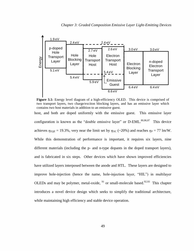
Chapter 3: Graded Composition Emissive Layer Light-Emitting Devices
49
host, and both are doped uniformly with the emissive guest. This emissive layer
configuration is known as the “double emissive layer” or D-EML.80,86,87
This device
achieves ηEQE = 19.3%, very near the limit set by ηOC (~20%) and reaches ηP = 77 lm/W.
While this demonstration of performance is important, it requires six layers, nine
different materials (including the p- and n-type dopants in the doped transport layers),
and is fabricated in six steps. Other devices which have shown improved efficiencies
have utilized layers interposed between the anode and HTL. These layers are designed to
improve hole-injection (hence the name, hole-injection layer, “HIL”) in multilayer
OLEDs and may be polymer, metal-oxide, 91
or small-molecule based.92,93
This chapter
introduces a novel device design which seeks to simplify the traditional architecture,
while maintaining high efficiency and stable device operation.
Figure 3.1: Energy level diagram of a high-efficiency OLED. This device is comprised of
two transport layers, two charge/exciton blocking layers, and has an emissive layer which
contains two host materials in addition to an emissive guest.
p-doped
Hole
Transport
Layer
Hole
Blocking
Layer
Hole
Transport
Host
Electron
Transport
Host Electron
Blocking
Layer
n-doped
Electron
Transport
Layer
1.9 eV
5.1 eV
2.4 eV
5.4 eV
2.7 eV
5.9 eV
2.6 eV
6.6 eV
3.0 eV
6.4 eV
3.0 eV
6.4 eV
2.4 eV
5.4 eV
Emissive
Guest
En
erg
y

Chapter 3: Graded Composition Emissive Layer Light-Emitting Devices
50
3.2 Graded-Composition Emissive Layer
The device architecture presented here was conceived as an exercise in
controlling the efficiency of exciton formation through the manipulation of injected
charge carriers in the emissive layer. To control the spatial extent of charge carriers in
the device, a layer whose composition varies continuously, from nearly 100% HTM at
the anode to nearly 100% ETM at the cathode, was fabricated with a constant doping of a
luminescent guest (Figure 3.2a). This layer structure was termed the “graded-emissive
layer” or G-EML. The fabrication of this layer was achieved through the co-deposition
of the three constituent materials using time-varying deposition rates, described in Figure
3.2b. This was made possible through the use of a VTE system where each material, and
rate monitor, is isolated from the others, and a carefully tuned PID controller with a
programmed, linear deposition rate ramp profile. Devices were fabricated in a single
process, using 4,4',4''-tris(carbazol-9-yl)triphenylamine (TCTA) as the HTM, 4,7-
Figure 3.2: (a) Schematic of a graded-composition layer. The HTM and ETM host materials
have a continuously-varying composition across the layer: from nearly 100% at the respective
electrode to 0% at the opposing electrode. The emissive guest concentration is kept constant
throughout the layer. (b) The deposition rate profiles of the constituent materials.
0 20 40 60 80 1000
10
20
30
40
50
60
70
80
90
100
Co
mp
ositio
n (
wt.
%)
Layer Thickness (nm)
HTM
ETM
GuestA
N
O
D
E
C
A
T
H
O
D
E
0 50 100 150 200 2500.0
0.4
0.8
1.2
1.6
2.0
2.4
2.8
3.2
3.6
4.0
Ra
te (
Å/s
)
Deposition Time (s)
HTM
ETM
Guest
(a) (b)
Chapter 3: Graded Composition Emissive Layer Light-Emitting Devices
51
diphenyl-1,10-phenanthroline (BPhen) as the ETM, and the archetypal green
phosphorescent guest, fac-tris(2-phenylpyridine) iridium (III) [Ir(ppy)3] , as the emitter at
an optimized concentration of 2 wt.%. The energy levels of these materials are shown in
Figure 3.3a.94,95
These host materials are well matched for optimum charge balance as
both are characterized by charge carrier mobilities of ~10-4
cm2
V-1
s-1
at an applied field
of ~105
V cm-1
.96,97
The G-EML structure was sandwiched between typical OLED electrodes: ITO as
an anode and LiF/Al as a cathode. For comparison, simplified OLEDs based on a D-
EML or a mixed-host emissive layer (M-EML) architecture were also fabricated. The M-
Figure 3.3: (a) Energy levels of the green light-emitting G-EML device. Layer structure of
the simplified (b) double-emissive layer, and (c) mixed emissive layer devices.
2.5 eV
5.6 eV
2.9 eV 3.0 eV
5.3 eV
6.4 eV
TCTA Ir(ppy)3 Bphen
Glass
ITO
BPhen:Ir(ppy)3 40 nm
LiF/Al
TCTA:Ir(ppy)3 40 nm
Double Emissive Layer
(D-EML)
Glass
ITO
LiF/Al
Mixed Emissive Layer
(M-EML)
TCTA:BPhen (1:1):Ir(ppy)3
80nm
(a)
(b) (c)

Chapter 3: Graded Composition Emissive Layer Light-Emitting Devices
52
EML architecture consists of a uniformly mixed distribution of ETM, HTM, and the
phosphorescent emitter in a set composition ratio. The result is a large interface area
between the ETM and HTM, creating favorable conditions for exciton formation.84,89,98
The layer structures for these additional devices is: 40 nm TCTA:Ir(ppy)3 (5 wt. %)/40
nm BPhen:Ir(ppy)3 (5 wt.%) for the D-EML (Figure 3.3b), and 80 nm
TCTA:BPhen:Ir(ppy)3 (1:1: 5 wt. %) for the M-EML (Figure 3.3c). The optimum
Ir(ppy)3 doping concentration was separately determined to be 5 wt.% for each of these
comparison architectures.
Previous work has demonstrated that the ηPL of phosphorescent materials may
approach unity in dilute-doped films (<2 wt. %).24
Unfortunately, conventional devices
using such low doping levels often show low efficiency and significant host
luminescence.25,57
This has been attributed to incomplete host-guest energy transfer or
inefficient charge trapping on the guest. In the G-EML, injected charge carriers are
initially carried by the respective transport materials into the device. At very low
concentration it is unlikely that Ir(ppy)3 participates in charge injection from the
electrodes or contributes significantly to charge transport. Due to the HOMO level
alignment between Ir(ppy)3 and TCTA, Ir(ppy)3 may act as a hole trap with excitons
forming directly on Ir(ppy)3.69,83,99
The combination of charge transport on the host
materials with direct exciton formation on the guest allows for the use of low doping
concentrations and thus the ability to realize a high ηPL for the guest. Figure 3.4a shows
the electroluminescence (EL) from OLEDs consisting of the D-EML, M-EML, or G-
EML already described. In each case Ir(ppy)3 emission is observed, with no emission

Chapter 3: Graded Composition Emissive Layer Light-Emitting Devices
53
from either host material. For the G-EML Figure 3.4b, the EL spectrum does not vary
with the applied current density. The lack of host emission supports a model of direct
charge-trapping for the excitation of Ir(ppy)3.
To further test this hypothesis, a 1:1 TCTA:BPhen G-EML OLED was fabricated
without Ir(ppy)3. This device was intended to explore the favored excited state of a G-
EML device without the emissive guest. Rather than exciting either of the host materials
independently, an exciplex (or excited complex) was formed; the EL spectrum is shown
in Figure 3.5. Given the HOMO/LUMO energy level alignment of TCTA with BPhen, it
is likely that the exciplex hole resides on a TCTA molecule and the electron on an
adjacent BPhen molecule. This is confirmed by comparing the TCTA-HOMO / BPhen-
LUMO energy gap, ~2.6 eV and the peak emission energy, λ ~ 470 nm (corresponding to
an energy of ~2.65 eV). This energy is well above the triplet excited state energy of
Ir(ppy)3 ~2.4 eV.100
This supports the model assumption that it is energetically
Figure 3.4: (a) Normalized EL spectra of M-EML, D-EML and G-EML OLEDs at a
brightness of 1000 cd/m2. (b) EL spectra of a G-EML OLED as a function of current density.
450 500 550 600 650 700
1 mA/cm2
10 mA/cm2
100 A/cm2
10 A/cm2
Inte
nsity
(a.
u.)
Wavelength (nm)
450 500 550 600 650 700
M-EML
D-EML
G-EML
Inte
nsity
(a.
u.)
Wavelength (nm)
(a) (b)

Chapter 3: Graded Composition Emissive Layer Light-Emitting Devices
54
unfavorable to from a host exciton; indeed, the lowest energy state in an Ir(ppy)3-doped
G-EML OLED is the guest exciton.
Figure 3.6a shows the current density-voltage characteristics of the three Ir(ppy)3-
based devices under consideration. Devices consisting of an M-EML exhibit the largest
leakage current at low voltage. Given that the M-EML devices have HTM and ETM
dispersed throughout the device, continuous conduction pathways for both holes and
electrons likely exist, permitting leakage currents to flow through the organic layer. In the
devices containing a D-EML, the separate layers of TCTA:Ir(ppy)3 and BPhen:Ir(ppy)3
present large energetic barriers for the leakage of electrons and holes, respectively. This
effectively confines charge carriers to the interface between the two emissive layers.80,87
In the G-EML device, large concentrations of TCTA near the anode and BPhen near the
cathode also prevent charge carriers from leaking across the device, confining them to the
central region of the G-EML.
Figure 3.5: Electroluminescence spectrum of a 1:1 TCTA:BPhen G-EML OLED without any
emissive guest.
350 400 450 500 550 600 650 700 7500.0
0.2
0.4
0.6
0.8
1.0
Norm
aliz
ed Inte
nsity (
a. u.)
Wavelength (nm)

Chapter 3: Graded Composition Emissive Layer Light-Emitting Devices
55
Figure 3.6b shows the luminance-voltage characteristics of OLEDs consisting
either of an M-EML, D-EML, or G-EML. The M-EML device requires the largest
voltage to realize measureable luminescence, having a turn-on voltage (“VTO” defined as
the voltage at which the brightness reaches 1 cd/m2) of VTO = 5.0 V. The combination of
low brightness and a high leakage current is an indication that the M-EML device suffers
from poor charge balance. The D-EML and G-EML architectures reach luminance levels
of ~100,000 cd/m2 and ~250,000 cd/m
2 at a voltage of 10 V, respectively. These devices
show high luminance at low voltage, with VTO = 2.6 V. Exciton formation on either
TCTA or BPhen would require an input energy at least as large as the optical energy gap
of each material, 3.3 eV and 3.4 eV respectively. These values are much larger than the
observed turn-on voltage. Additionally, the energetic barriers for electron injection into
TCTA and hole injection into BPhen are large, while it is favorable for holes to reside on
Figure 3.6: (a) Current density-voltage and (b) luminance-voltage characteristics for M-EML
(square), D-EML (circle), and G-EML (triangle) OLEDs.
(b)(a)
0.1 1 1010
-7
10-6
10-5
10-4
10-3
10-2
10-1
100
101
102
103
104
M-EML
D-EML
G-EML
Cu
rre
nt
De
nsity (
mA
/cm
2)
Voltage (V)2 4 6 8 10
10-1
100
101
102
103
104
105
106
Lu
min
an
ce
(cd
/m2)
Voltage (V)

Chapter 3: Graded Composition Emissive Layer Light-Emitting Devices
56
Ir(ppy)3. This is additional evidence for the direct formation of excitons on Ir(ppy)3. The
G-EML device shows an enhancement in brightness at high voltage, indicating that
charge balance is improved over the D-EML device.
The dependence of the external quantum efficiency and power efficiency on
current density is shown in Figure 3.7a and 3.7b. The poor charge balance in the M-EML
device has a detrimental effect on its overall performance, with an ηEQE = (0.22 ± 0.03) %
and ηP = (0.25 ± 0.03) lm/W. Improved charge confinement in the D-EML enhances
charge balance compared to the M-EML device, leading to peak efficiencies of
ηEQE = (11.8 ± 0.3) % and ηP = (39.4 ± 2.6) lm/W. Owing to the self-balancing nature of
the G-EML, charge balance is nearly maximized. This leads to a high external quantum
efficiency of (16.9 ± 0.4) % and a power efficiency of (61.0 ± 1.1) lm/W.
Figure 3.7: External quantum (a) and power (b) efficiency versus current density for M-EML
(square), D-EML (circle), and G-EML (triangle) OLEDs. At 1000 cd/m2
the D-EML OLED
has ηEQE = 11.7% and ηP = 28.7 lm/W, while the G-EML OLED has ηEQE = 16.7% and ηP =
44.4 lm/W.
(a) (b)
10-3
10-2
10-1
100
101
102
103
104
0
2
4
6
8
10
12
14
16
18
G-EML
D-EML
M-EML
Exte
rna
l Q
ua
ntu
m E
ffic
ien
cy (
%)
Current Density (mA/cm2)
10-3
10-2
10-1
100
101
102
103
104
0
10
20
30
40
50
60G-EML
D-EML
M-EML
Po
we
r E
ffic
ien
cy (
lm/W
)
Current Density (mA/cm2)

Chapter 3: Graded Composition Emissive Layer Light-Emitting Devices
57
3.3 Optimizing Red G-EML OLEDs
In addition to the green-light emitting G-EML devices, it is also desirable to
achieve high efficiency operation in both red- and blue-light emitting devices. Taken
together, these three, “primary colors of light,” allow for a spectral distribution which
spans the visible wavelength region, enabling both display and white-light applications.
Display applications require saturated color spectra; that is, they require deep blue, deep
red, and green emission to cover the whole range of spectra needed to display colors.
Lighting applications, however, require that all wavelengths of visible light are produced,
so that reflections off of objects accurately reflect their color (as compared to a blackbody
source, like the sun). Thus, the optimal spectrum of colors differs for lighting and display
applications and different emitting molecules are required. The optimization of these
structures depends on the constituent materials chosen, and is discussed below.
Figure 3.8: EL spectrum of PQIr in a G-EML OLED. The inset shows the chemical
structure together with the HOMO and LUMO energy levels, taken from literature.
350 400 450 500 550 600 650 700 750 800 8500.0
0.2
0.4
0.6
0.8
1.0
No
rma
lize
d In
ten
sity (
a.
u.)
Wavelength (nm)
2.7 eV
5.0 eV

Chapter 3: Graded Composition Emissive Layer Light-Emitting Devices
58
3.3.1 Red-Light Emitting G-EML OLEDs for Display Applications
Red light-emitting G-EML OLEDs were fabricated using bis(1-
phenylisoquinoline)-(acetylacetonate) iridium (III) [PQIr] as the emissive guest. The EL
spectrum of the molecule is shown in Figure 3.8, together with the molecular structure
and energy levels. The spectrum peaks at ~630 nm and has spectral components which
extend into the deep red and near-IR regions of the electromagnetic spectrum. This
spectrum makes PQIr a good candidate for display applications. Given that the energy
levels of this molecule fall within those of Ir(ppy)3, it follows that a similar G-EML host
configuration should also permit efficient device performance. Indeed, peak performance
is achieved for the same host structure shown in Figure 3.2b, with TCTA and BPhen as
HTM and ETM, with a slightly higher optimal doping concentration of 7 wt.%
The current density-voltage and brightness voltage-characteristics of the device
are shown in Figure 3.9a. Like the Ir(ppy)3-based G-EML devices, the PQIr-based G-
Figure 3.9: (a) Current density-voltage and brightness-voltage characteristics of PQIr-based
G-EML OLED. (b) ηEQE and ηP versus current density. Peak ηEQE = 12.7% and ηP = 7.5
lm/W are achieved.
0.1 1 1010
-7
10-6
10-5
10-4
10-3
10-2
10-1
100
101
102
103
104
10-2
10-1
100
101
102
103
104
105
106
Curr
ent
Density (
mA
/cm
2)
Voltage (V)
Brightn
ess (
cd/m
2)
10-3
10-2
10-1
100
101
102
0
1
2
3
4
5
6
7
8
9
10
11
12
13
14
0
1
2
3
4
5
6
7
8
9
10
EQ
E (
%)
Current Density (mA/cm2)
Po
wer
Eff
icie
ncy (
lm/W
)
(a) (b)

Chapter 3: Graded Composition Emissive Layer Light-Emitting Devices
59
EML OLEDs show a low leakage current at low voltage, with a steep increase in current
density which coincides with a steep increase in the luminance of the device. The turn-on
voltage of the device is VTO = 2.9V, indicating an efficient use of voltage. The ηEQE and
ηP of the PQIr-based device are shown in Figure 3.9b. Given that the ηPL of PQIr is
~60% and with an initial guess that ηOC ~20%, an ηEQE = 12.7% represents a near unity
ηIQE.24
The relatively low value of ηP for this device is the result of the poor overlap in
the spectrum of PQIr with the photopic response function. Given the deep-red EL
spectrum, PQIr would be a good candidate for display applications, though the IR
components would represent a loss in white-lighting applications.
3.3.2 Red-Light Emitting G-EML OLEDs for Lighting Applications
To address the need for lighting application-specific devices, a new red-orange
emissive guest is chosen, Bis(phenylisoquinoline)(2,2,6,6-tetramethylheptane-3,5-
dionate) iridium(III) [Ir(dpm)pq2]. The EL spectrum for this molecule is shown in Figure
Figure 3.10: EL spectrum of PQIr in a G-EML OLED. The inset shows the chemical
structure.
350 400 450 500 550 600 650 700 750 8000.0
0.2
0.4
0.6
0.8
1.0
Inte
nsity (
a.
u.)
Wavelength (nm)

Chapter 3: Graded Composition Emissive Layer Light-Emitting Devices
60
3.10 with the chemical structure. While the shape is similar to PQIr, the spectrum is
shifted to higher energies, with a peak wavelength of ~600 nm and much less emission in
the near-IR. The current density-voltage and brightness-voltage characteristics of a 1:1 G-
EML device with TCTA and BPhen are shown in Figure 3.11a. The current density-
voltage characteristics of the Ir(dpm)pq2-based devices show the low leakage current
characteristic of the optimized G-EML device. Likewise, a low VTO = 2.75 V is achieved,
indicating very efficient voltage use. The ηEQE and ηP of the device are shown in Figure
3.11b. With ηPL ≈ 70%, a peak ηEQE = 12.1% represents a very high ηIQE ≈ 85%.101
With
the improved spectral overlap of the EL spectrum with the photopic response function, a
peak ηP = 23 lm/W is achieved. All together, the ηEQE, ηP, and red-orange spectra of the
Ir(dpm)pq2-based G-EML OLEDs render these devices promising candidates for
inclusion into white lighting applications.
Figure 3.11: (a) Current density-voltage and brightness-voltage characteristics of Ir(dpm)pq2-
based GEML OLED. (b) ηEQE and ηP versus current density. Peak ηEQE = 12.1% and ηP =
23.0 lm/W are achieved.
10-4
10-3
10-2
10-1
100
101
102
103
104
0
2
4
6
8
10
12
14
0
2
4
6
8
10
12
14
16
18
20
22
24
EQ
E (
%)
Current Density (mA/cm2)
Po
wer
Eff
icie
ncy (
lm/W
)
0.1 1 1010
-7
10-6
10-5
10-4
10-3
10-2
10-1
100
101
102
103
104
10-3
10-2
10-1
100
101
102
103
104
105
106
Curr
ent
Density (
mA
/cm
2)
Voltage (V)
Bri
gh
tne
ss (
cd
/m2
)
(a) (b)
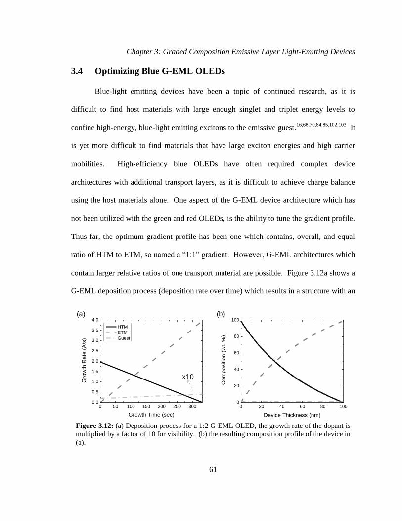
Chapter 3: Graded Composition Emissive Layer Light-Emitting Devices
61
3.4 Optimizing Blue G-EML OLEDs
Blue-light emitting devices have been a topic of continued research, as it is
difficult to find host materials with large enough singlet and triplet energy levels to
confine high-energy, blue-light emitting excitons to the emissive guest.16,68,70,84,85,102,103
It
is yet more difficult to find materials that have large exciton energies and high carrier
mobilities. High-efficiency blue OLEDs have often required complex device
architectures with additional transport layers, as it is difficult to achieve charge balance
using the host materials alone. One aspect of the G-EML device architecture which has
not been utilized with the green and red OLEDs, is the ability to tune the gradient profile.
Thus far, the optimum gradient profile has been one which contains, overall, and equal
ratio of HTM to ETM, so named a “1:1” gradient. However, G-EML architectures which
contain larger relative ratios of one transport material are possible. Figure 3.12a shows a
G-EML deposition process (deposition rate over time) which results in a structure with an
Figure 3.12: (a) Deposition process for a 1:2 G-EML OLED, the growth rate of the dopant is
multiplied by a factor of 10 for visibility. (b) the resulting composition profile of the device in
(a).
0 50 100 150 200 250 3000.0
0.5
1.0
1.5
2.0
2.5
3.0
3.5
4.0
Gro
wth
Ra
te (
A/s
)
Growth Time (sec)
HTM
ETM
Guest
0 20 40 60 80 1000
20
40
60
80
100
Com
positio
n (
wt. %
)
Device Thickness (nm)
(a) (b)
x10

Chapter 3: Graded Composition Emissive Layer Light-Emitting Devices
62
overall relative ratio of 1:2 HTM to ETM, the compositional structure of the device is
shown in Figure 3.12b.
Indeed, a continuous range of gradient profiles which favor one type of host
material are possible with a naming convention which refers to the overall ratio of the
host materials, HTM:ETM. Importantly, these devices retain the nearly 100% host
composition at each respective electrode and continuously vary to nearly 0% composition
at the opposing electrode. This tunability allows for the use host materials which have
desirable exciton energy levels, but which may not have optimal charge carrier
mobilities. This flexibility widens the library of possible host material combinations,
where particular materials are desired.
3.4.1 Blue Light-Emitting Devices with TPBi as an ETL
To achieve blue light emission, the phosphorescent guest molecule bis[(4,6-
difluorophenyl)-pyridinatoN,C2’
]picolinate (FIrpic) was chosen. The EL spectrum of this
molecule is shown in Figure 3.13 with the energy levels and chemical structure. The
triplet energy of this emitter is ~2.65 eV, with a peak EL emission wavelength of ~475
Figure 3.13: Electroluminescent spectrum of FIrpic, the energy levels and molecular structure
are inset.
350 400 450 500 550 600 650 700 7500.0
0.2
0.4
0.6
0.8
1.0
No
rma
lize
d In
ten
sity (
a.
u.)
Wavelength (nm)
3.0 eV
5.9 eV

Chapter 3: Graded Composition Emissive Layer Light-Emitting Devices
63
nm.16,70
As per the discussion above, a suitable host must have a triplet energy at least
equal to, but preferably higher than, the triplet energy of FIrpic. While TCTA qualifies
(ET ≈ 2.9 eV), BPhen does not (ET ≈ 2.5 eV).66,104
A recently developed molecule with
high triplet energies and suitable HOMO and LUMO energies was chosen as an ETM:
2,2’,2’’-(1,3,5-benzinetriyl)-tris(1-phenyl-1-H-benzimidazole) (TPBi, ET = 2.7 eV,
HOMO = 2.8 eV, LUMO = 6.3 eV).89
A series of G-EML devices were constructed with varying gradient profiles to
determine the optimal balance of HTM:ETM, the peak ηEQE of each device is plotted in
Figure 3.14a with the chemical structure of TPBi inset. The performance of the G-EML
improves with increasing TPBi concentration up to a critical threshold where
performance rolls of steeply. The best performing device has a 1:2 gradient profile, with
peak ηEQE =10.9%, and peak ηP =28.1 lm/W. To better understand the origin of this
performance trend, the VTO and the voltage at 1000 cd/m2 for each device are plotted in
Figure 3.14b. The VTO shows a weak dependence on composition, except for extreme
Figure 3.14: (a) Peak ηEQE of varying composition profile of FIrpic-based G-EML devices.
TCTA is used as an HTM with TPBi as an ETM. The molecular structure of TPBi is shown in
the inset. (b) The turn-on voltage (voltage at 1 cd/m2) and the voltage required to produce
1000 cd/m2 as a function overall TPBi concentration.
30 40 50 60 70 800
2
4
6
8
10
12
Pe
ak E
QE
(%
)
TPBi concentration (wt. %)
0.3 0.4 0.5 0.6 0.7 0.82.6
2.7
2.8
2.9
3.0
3.1
3.2
3.3
3.4
4.0
4.5
5.0
5.5
6.0
6.5
7.0
7.5
8.0
Vo
lta
ge
at
1 c
d/m
2
TPBi concentration (wt. %)
Vo
lta
ge
at
10
00
cd
/m2
(a) (b)

Chapter 3: Graded Composition Emissive Layer Light-Emitting Devices
64
gradient profiles. This likely reflects the fact that injection into the device is not affected,
until extreme gradient profiles render the active layer a vast majority of ETM. The
voltage at higher output, however, shows a strong trend with composition, with the
optimal gradient for efficient voltage use matching the gradient profile for ηEQE. This
indicates that tuning the gradient profile not only influences the charge carrier
distributions and the ease with which they may form excitons (indicated by lower
voltage), but also the degree of charge carrier confinement in the device. With FIrpic
doped throughout the device, excitons formed anywhere within the organic layers will
decay with high ηPL (this is further confirmed by the lack of host emission in these
devices); thus, reductions in the peak ηEQE must come from a loss in charge balance,
which in these single-layer devices, is manifested as the transport of a carrier from one
electrode, across the layer, to the opposite electrode. The electrical properties of these G-
EML devices will be explored more in Chapter 5.
3.4.2 Blue Light-Emitting Devices with 3TPYMB
The peak ηEQE of the previous FIrpic-based devices is well below the theoretical
limit, considering ηOC ≈ 20% and ηPL ≈ 95% at low concentration (giving a peak ηEQE =
19.0%).24
The ηPL of FIrpic doped in to TPBi has recently been discussed, where it was
found that the ηPL reached a maximum value of only 32% at a concentration of 10 wt.
%.64
This low efficiency was attributed to a back-transfer of excitons from FIrpic to
TPBi, given the relatively close triplet energy levels. Thus, to achieve higher peak
efficiencies using FIrpic, a wider-gap ETM was chosen to replace TPBi: Tris(2,4,6-
trimethyl-3-(pyridin-3-yl)phenyl)borane (3TPYMB). A series of gradient profiles (2:1,

Chapter 3: Graded Composition Emissive Layer Light-Emitting Devices
65
1:1, and 1:2) were fabricated using TCTA and 3TPYMB as the HTM and ETM hosts,
respectively, with 2 wt.% FIrpic. The current density-voltage characteristics of the three
devices are shown in Figure 3.15a along with the molecular structure and energy levels of
3TPYMB. The resulting ηEQE of the various devices are shown in Figure 3.15b.
Again, the 1:2 gradient profile shows the lowest voltage (VTO = 2.75 V) and highest peak
performance (ηEQE = 16.1% and ηP = 35.5 lm/W) of the three devices. This performance
represents an enhancement in ηEQE of nearly 50% over the TPBi-based devices.
3.4.3 Multilayer FIrpic-Based OLEDs
Given the high ηPL of FIrpic, a device was fabricated which replicated a known,
highly efficient OLED. This device replaced TCTA with another wide-gap HTM: Di-[4-
(N,N-ditolyl-amino)-phenyl]cyclohexane (TAPC) and utilized a newly synthesized ETM:
2,8-bis(diphenylphosphoryl)dibenzothiophene (PO15), obtained from Pacific Northwest
Figure 3.15: (a) Current density-voltage characteristics of the TCTA:3TPYMB-based FIrpic
G-EML devices. The molecular structure and energy levels of 3TPYMB are shown in the
inset. (b) The ηEQE of the three gradient profiles versus current-density. The 1:2 gradient
profile shows the highest peak ηEQE = 16.1%.
0.1 1 1010
-9
10-7
10-5
10-3
10-1
101
103
2:1 Profile
1:1 Profile
1:2 Profile
Curr
ent
Density (
mA
/cm
2)
Device Voltage (V)
2.8 eV
6.7 eV
10-4
10-3
10-2
10-1
100
101
102
103
104
0
5
10
15
20
EQ
E (
%)
Current Density (mA/cm2)
2:1 Profile
1:1 Profile
1:2 Profile
(a) (b)
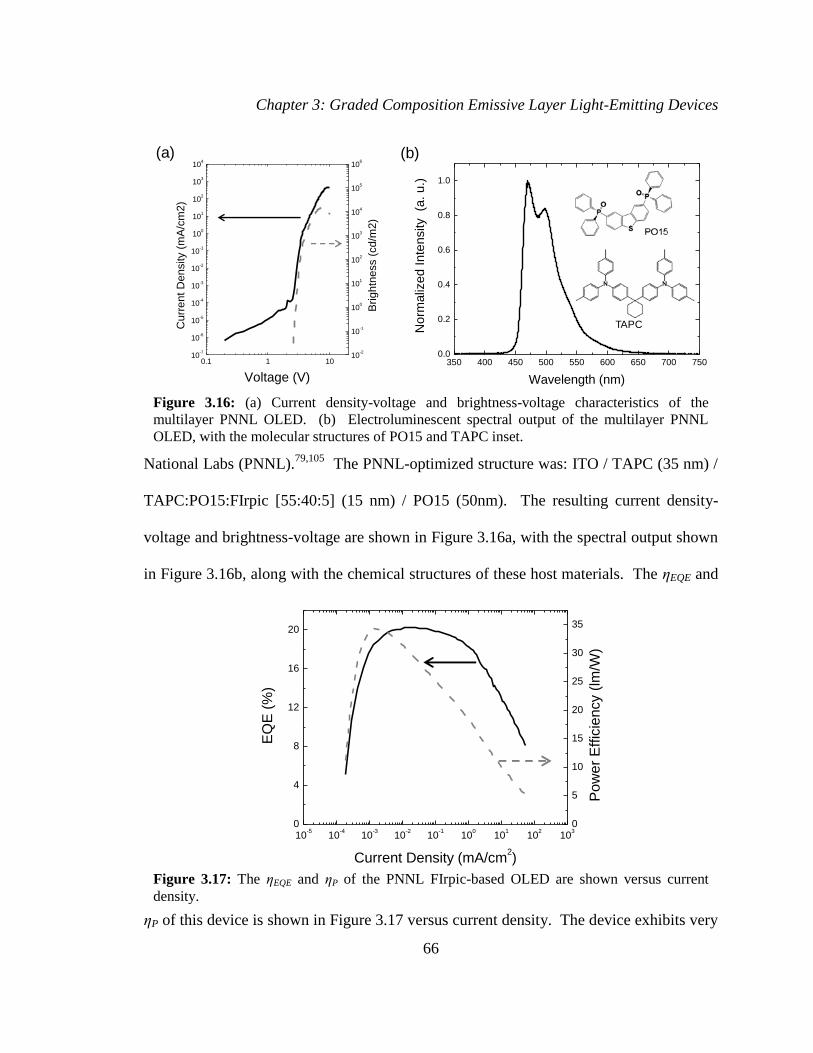
Chapter 3: Graded Composition Emissive Layer Light-Emitting Devices
66
National Labs (PNNL).79,105
The PNNL-optimized structure was: ITO / TAPC (35 nm) /
TAPC:PO15:FIrpic [55:40:5] (15 nm) / PO15 (50nm). The resulting current density-
voltage and brightness-voltage are shown in Figure 3.16a, with the spectral output shown
in Figure 3.16b, along with the chemical structures of these host materials. The ηEQE and
ηP of this device is shown in Figure 3.17 versus current density. The device exhibits very
Figure 3.17: The ηEQE and ηP of the PNNL FIrpic-based OLED are shown versus current
density.
10-5
10-4
10-3
10-2
10-1
100
101
102
103
0
4
8
12
16
20
0
5
10
15
20
25
30
35
EQ
E (
%)
Current Density (mA/cm2)
Po
we
r E
ffic
ien
cy (
lm/W
)
Figure 3.16: (a) Current density-voltage and brightness-voltage characteristics of the
multilayer PNNL OLED. (b) Electroluminescent spectral output of the multilayer PNNL
OLED, with the molecular structures of PO15 and TAPC inset.
350 400 450 500 550 600 650 700 7500.0
0.2
0.4
0.6
0.8
1.0
Norm
aliz
ed Inte
nsity (a
. u.)
Wavelength (nm)
0.1 1 1010
-7
10-6
10-5
10-4
10-3
10-2
10-1
100
101
102
103
104
10-2
10-1
100
101
102
103
104
105
106
Curr
ent
Density (
mA
/cm
2)
Voltage (V) B
rightn
ess (
cd/m
2)
TAPC
(a) (b)

Chapter 3: Graded Composition Emissive Layer Light-Emitting Devices
67
high peak quantum- and power-efficiencies of ηEQE = 20.3%, ηP = 34.3 lm/W . The
comparison of this data to the previously fabricated FIrpic-based G-EML devices
indicates that an enhancement of ~20% is achievable through further optimization. This
optimization will likely come from minor changes to the device such as small changes in
doping concentration, which will not drastically alter the operation of the G-EML device.
3.5 Conclusion
In summary, a graded-emissive layer device architecture has been presented
which achieves high-efficiency device operation and is fabricated in a single deposition
process. The efficiencies achieved here approach those of state-of-the-art, multilayer
devices, despite the simple device architecture. Through the use of various emitting
molecules, the G-EML architecture may be extended to devices of all visible-wavelength
emission colors. The importance of host selection and gradient profile has been
demonstrated experimentally. Clearly, the change in host material is responsible for the
improvement in ηEQE observed in the FIrpic-based G-EML OLEDs presented here.
Further, tuning the gradient profile allows for a wide variety of host materials to be
considered. Imbalances in the charge carrier mobilities of the hosts may be overcome
through tuning of the composition profile. The impact of gradient profile on charge
carrier mobility is examined in greater detail in Chapter 4.

Chapter 4: Depth Profiling of Organic Thin Films
68
Chapter 4 - Depth Profiling of Organic Thin Films
The previous chapters have demonstrated the important role of device and
emissive layer engineering in organic light-emitting device (OLED) operation and
performance. Highly efficient devices often contain layers which are comprised of
multiple materials with different functionalities. This is particularly true for the emissive
layer, where a dilute emissive guest molecule is often doped into a host material, as in the
case of a double-emissive layer (D-EML) or mixture of host materials, in the case of a
mixed-emissive layer (M-EML);13,56,87,106
though composite transport layers are also
used.61,80,107
The overall composition and composition profile of these layers have
proven difficult to probe,108–110
as the thin films are typically soft and the different
molecules are often composed only of carbon, hydrogen, and nitrogen.83
The
performance of these composite layers has been shown to be strongly dependent on the
mixing ratio and spatial distribution of the constituent materials. This is especially
evident in the M-EML device, where the mixing ratio of hole- and electron-transport
material (HTM and ETM, respectively) significantly impacts device
performance.79,84,89,111,112
More recently, devices employing a graded-emissive layer (G-
EML) architecture, where the emissive layer is comprised of a continuously varying
composition of HTM, ETM, and emissive guest, have demonstrated high efficiency in
single-layer devices.113,114
These G-EML devices show a strong dependence of
performance on the exact composition profile, and the optimized blue light-emitting

Chapter 4: Depth Profiling of Organic Thin Films
69
devices of Chapter 3 have composition profiles which contain relatively larger amounts
of ETM.115
Typically, devices with composite layers are fabricated via vacuum thermal co-
evaporation. While this fabrication technique allows for careful control over the relative
deposition rates of the constituent materials, the spatial composition of these films have
proven difficult to examine post-deposition. Given the demonstrated connection between
film composition and device performance, there is strong interest in developing
techniques to accurately probe the exact post-deposition composition profile.
Characterization of the depth profile requires a means to determine both the identity and
quantity of chemical species present at the surface of the film (or within a very shallow
volume near the surface), so that exact ratios of the constituent materials may be
determined. Additionally, a process to remove thin, uniform layers of material from
cathode to anode is required. This process must not damage the underlying layers nor
chemically interact with the exposed surface.
Until recently, the sputtering of organic thin films has focused on the use of C60+
ion beams to remove thin layers of material.108,110
Though this method has shown some
positive results, it is not applicable to many organic systems where the deposition of
amorphous carbon and chemical interactions at the surface render analysis of the
underlying layers impossible.108,116
Promising results, however, have been obtained
using large-clusters of Ar ions as the primary beam in gas-cluster ion beam (GCIB)
milling with time-of-flight secondary ion mass spectrometry (TOF-SIMS) analysis. The

Chapter 4: Depth Profiling of Organic Thin Films
70
Ar-GCIB process has shown large sputtering yields of organic materials with little signs
of degradation of the exposed layers.109,117
One of the primary drawbacks of the TOF-
SIMS chemical analysis technique is its inability to easily quantify the various chemical
states without elaborate standards and calibration processes.
4.1 X-ray Photoelectron Spectroscopy
An alternative technique, which allows for a quantitative measurement of the
chemical makeup of the surface of an organic thin film is X-ray photoelectron
spectroscopy (XPS).118,119
In this technique, high energy monochromatic X-rays are
focused to small spot on the surface of the sample. The X-rays are generated through the
use of an electron gun aimed at an Al target. Electron impact on the Al target generates
X-rays with an energy of 1486.6 eV. These X-rays penetrate the organic sample and
interact with the electron orbitals of the constituent atoms of each molecule. Electrons
near the sample surface are ejected with kinetic energies characteristic of their binding
energies in each molecule. The XPS technique is non-destructive and is capable of
detecting very small differences in the chemical makeup of many organic semiconducting
materials. In this work, sequential Ar-based GCIB sputtering is paired with XPS
measurements to allow for the composition depth profile of an organic thin film to be
determined.
4.2 Experimental Techniques
All organic thin films and devices were fabricated according to the previously
reported methods, using 4,4',4''-tris(carbazol-9-yl)triphenylamine (TCTA) as an HTM,

Chapter 4: Depth Profiling of Organic Thin Films
71
4,7-diphenyl-1,10-phenanthroline (BPhen) as an ETM, and fac-tris(2-phenylpyridine)
iridium (III) (Ir(ppy)3) as the emissive guest. Samples were packed in a nitrogen
environment and transported to the composition depth profiling system where they were
loaded from ambient to a load-locked antechamber. The samples of interest were
characterized in a PHI VersaProbe II Scanning XPS system equipped with an Ar+ Gas
Cluster Ion Beam source for depth profiling. Since the device structures were large and
uniform, XPS measurements were done with a 200 μm monochromatic Al Kα (1486.6
eV) X-rays focused on the area of interest. The photoelectron takeoff angle was 45° and
the pass energy in the spherical capacitance analyzer was fixed at 23 eV for this analysis
to obtain good energy resolution to clearly define both the C 1s and N 1s species in
TCTA and BPhen. The GCIB source can be operated with beam energies from 2.5 kV to
20 kV and Ar cluster size from <1000 to 5000. For this study we used Ar1500 clusters at
10 kV, 2 nA corresponding to 4 eV per Ar+ atom rastering over a 2 mm x 2 mm area.
The PHI VersaProbe II Scanning XPS system has a dual beam charge neutralization (7
eV Ar+ ions and 1 eV electrons) capability to prevent differential surface charging at
various interfaces.
4.3 XPS Study of Host Materials
Initial C 1s and N 1s XPS spectra of pure films of TCTA and BPhen are shown in
Figures 4.1a with the chemical structures shown in the inset. Though both materials are
comprised of only carbon, hydrogen, and nitrogen, a distinct chemical signature is
recorded. The N 1s peak of TCTA is shifted by 1.8 eV relative to BPhen (Figure 4.1b),

Chapter 4: Depth Profiling of Organic Thin Films
72
this is due to the difference in electronic environments of the nitrogen atom in each
molecule. This shift serves as a unique identification of the two materials in subsequent
measurements and highlights the high resolution chemical state characterization of the
XPS technique. It is interesting to view the complete XPS scan of BPhen on
an ITO/glass substrate, Figure 4.2. Here, signal from the ITO substrate is apparent in the
initial BPhen scan, before the first Ar-GCIB sputter process. This is likely due to the
Figure 4.1: XPS spectra of the N 1s and C 1s of (a) TCTA and (b) BPhen. The N 1s peaks
are shifted, relative to each other, by 1.8 eV.
0
20
40
60
80
100
120
TCTA
N 1s
Inte
nsity (
counts
x 1
02/s
ec)
TCTA C 1s
405 400 395 295 290 285 280
0
5
10
15
20
25
30
35
BPhen
Binding Energy (eV)
C 1sBPhen
N 1s
404 402 400 398 3960
2
4
6
8
10
12
14
16
18
Inte
nsity (
counts
x 1
02/s
ec)
Binding Energy (eV)
(a)
(b)

Chapter 4: Depth Profiling of Organic Thin Films
73
crystallization of BPhen after exposure to atmosphere, which results in the formation of
voids. According to Figure 4.2, these voids are present throughout the entire depth of the
sample. To protect the BPhen layer a sample was grown on TCTA which was capped
with a thin (10nm) layer of TCTA to encapsulate and protect the BPhen surface. The
stack was subjected to the depth profiling process; the resulting composition profile is
presented in Figure 4.3. It is clear that neither the Si substrate used here, nor the
underlying TCTA layer, are detected in the initial scan or in subsequent depth scans, until
most of the BPhen layer has been sputtered. This indicates the role of ambient
atmosphere in inducing crystallization in BPhen and suggests that BPhen crystallization
does not occur during growth, but rather is an environmental effect which may be
mitigated with the use of a capping layer.
Figure 4.2: Full XPS spectra of a 100-nm-thick layer of BPhen on ITO.
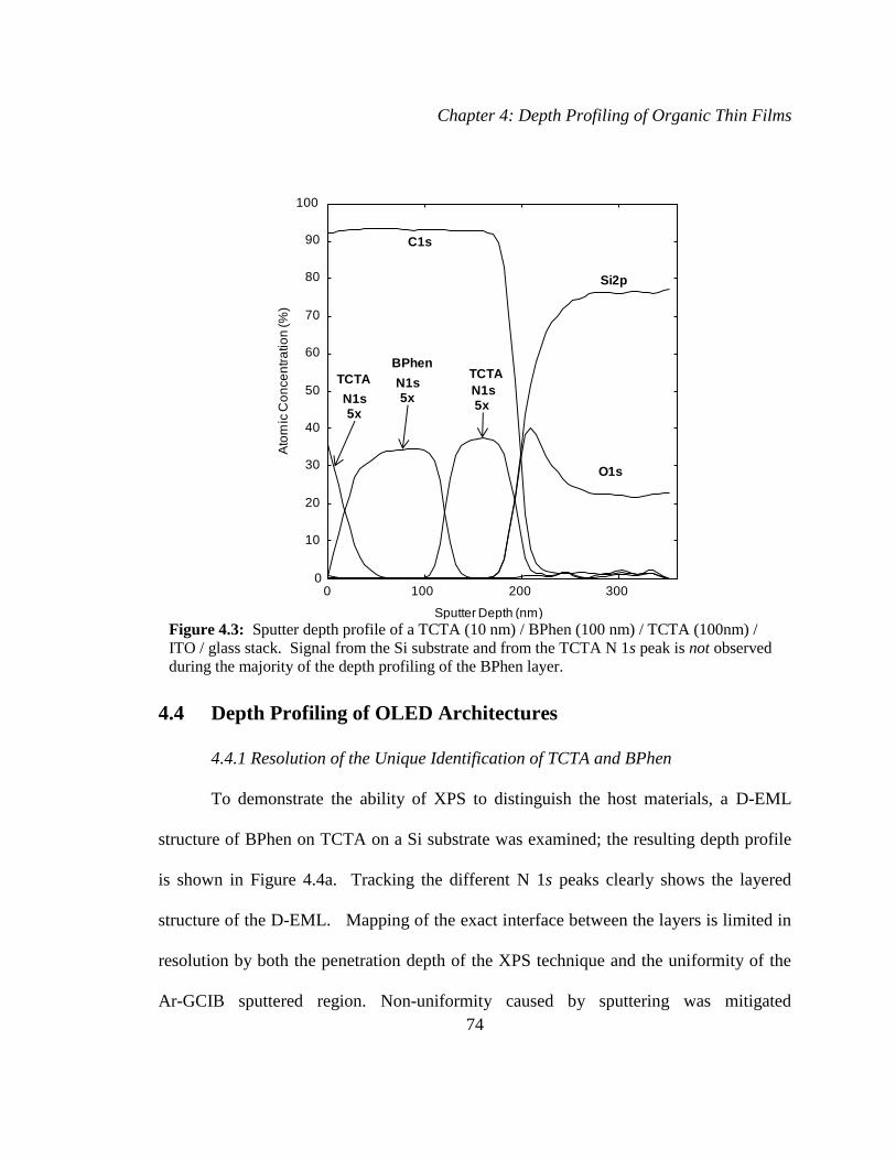
Chapter 4: Depth Profiling of Organic Thin Films
74
4.4 Depth Profiling of OLED Architectures
4.4.1 Resolution of the Unique Identification of TCTA and BPhen
To demonstrate the ability of XPS to distinguish the host materials, a D-EML
structure of BPhen on TCTA on a Si substrate was examined; the resulting depth profile
is shown in Figure 4.4a. Tracking the different N 1s peaks clearly shows the layered
structure of the D-EML. Mapping of the exact interface between the layers is limited in
resolution by both the penetration depth of the XPS technique and the uniformity of the
Ar-GCIB sputtered region. Non-uniformity caused by sputtering was mitigated
Figure 4.3: Sputter depth profile of a TCTA (10 nm) / BPhen (100 nm) / TCTA (100nm) /
ITO / glass stack. Signal from the Si substrate and from the TCTA N 1s peak is not observed
during the majority of the depth profiling of the BPhen layer.
0 100 200 3000
10
20
30
40
50
60
70
80
90
100
Sputter Depth (nm)
Ato
mic
Co
nce
ntr
atio
n (%
)
C1s
TCTABPhen
TCTA
O1s
Si2p
N1s5x
N1s5xN1s
5x

Chapter 4: Depth Profiling of Organic Thin Films
75
by using compucentric Zalar (® Physical Electronics) rotation of the sample during the
sputter cycle.
4.4.2 Characterization of the Mixed-Emissive Layer
The XPS spectra for the C 1s and N 1s peaks of a M-EML device on ITO are
shown as a function of sputter depth in Figure 4.5a and 4.5b, respectively. The π-π*
shake-up transition in the C 1s spectra is clearly identifiable for each sputter depth. The
persistence of this peak throughout the sputter depth of the organic film demonstrates that
the depth profiling process does not damage the conjugation of the target molecules. The
XPS spectra of the N 1s peak clearly show the 400.4 eV peak present in TCTA and the
Figure 4.4: Depth profile of a BPhen / TCTA D-EML structure.
0 10 20 30 40 500
10
20
30
40
50
60
70
80
90
100
Sputter Time (min)
Ato
mic
Co
nce
ntr
atio
n (%
)
N1s 5xBPhen
N1s 5xTCTA
C1s
O1s
Si 2p

Chapter 4: Depth Profiling of Organic Thin Films
76
398.6 eV peak of BPhen. The complete depth profile of the M-EML is shown in Fig.
4.5c. The composition of the M-EML device clearly shows that the uniform mixing of
TCTA and BPhen is maintained throughout the layer and persists post-deposition. No
large-scale vertical separation of the two phases is observed within the resolution of the
technique.
Figure 4.5: XPS spectra for (a) C 1s and (b) N 1s peaks for a M-EML device on an ITO
substrate. The complete depth profile of the device is shown in (c).
50 100 150 2000
10
20
30
40
50
60
70
80
90
100
Sputter Depth (nm)
Ato
mic
Co
nce
ntr
atio
n (%
)
N1s 5x
BPhen
N1s 5x
TCTA
C1s
O1s
In3d5
(a) (b)
(c)

Chapter 4: Depth Profiling of Organic Thin Films
77
Figure 4.6: Composition depth profiles of (a) 1:1, (b) 1:2, (c) and 1:3 gradient profiles of
TCTA:BPhen. The predicted gradient profiles for BPhen (squares) and TCTA (circles) are
shown overlaid on the depth profile data.
0
50
100 Predicted
BPhen
TCTA
Co
mp
ositio
n (
wt. %
)
50 1000
102030405060708090
100
Sputter Depth (nm)
Ato
mic
Concentr
atio
n (%
)
N 1s 5xBPhen
N 1s 5x
TCTA
C1s
O 1s
Si 2p
1:2 Gradient
0
50
100
Com
positio
n (
wt. %
)
Predicted
BPhen
TCTA
0 50 100
102030405060708090
100
Sputter Depth (nm)
Ato
mic
Concentr
atio
n
(%)
C 1s
Si 2p
O 1sN 1s 5x
BPhen
N 1s 5xTCTA
1:3 Gradient
0
50
100 Predicted
BPhen
TCTA
Com
positio
n (
wt. %
)
0 50 100 150Sputter Depth (nm)
C 1s
O 1s
In 3d
N 1s 5x
BPhenN 1s 5x
TCTA
1:1 Gradient
102030405060708090
100
Ato
mic
Concentr
atio
n (%
)
(a)
(b)
(c)
Chapter 4: Depth Profiling of Organic Thin Films
78
4.4.3 Characterization of the Graded-Emissive Layer
The composition depth profiles of G-EML devices having 1:1, 1:2, and 1:3
TCTA:BPhen composition ratios are shown in Figures 4.6a, b, and c, respectively, along
with the target profiles. It is clear that each composition profile is physically distinct.
The measured composition profile matches closely with the intended composition profile,
both in the concentration ratio of the host materials at each location and in the zero-
concentration endpoints of the intended gradient profile. From this data, it follows that
the observed differences in device operation and performance are the product of real
differences in the electronic properties of each gradient, which are the result of distinct
variations of the spatial composition in each G-EML device. The close matching of the
intended and measured composition profiles indicates that vapor-deposition is a reliable
way to achieve robust, graded-composition layers that do not greatly phase-separate
during growth or post deposition, and whose electronic properties may be tuned by small
changes in gradient composition profile.
4.5 Conclusion
In conclusion, the pairing of Ar-GCIB with XPS allows for the examination of the
composition depth profile of OLEDs to be examined with great precision. The large-
cluster Ar-GCIB process is well-suited for use with soft organic thin-films as it does not
contaminate the surface nor damage the underlying layers. The use of XPS allows for
precise quantification and identification of the various molecular species found
throughout the depth of an OLED device. These techniques have been used to examine

Chapter 4: Depth Profiling of Organic Thin Films
79
the composition depth profiles of a variety of common OLED emissive layer
architectures fabricated via vacuum thermal deposition, and confirm that variations in the
intended composition profiles of G-EML devices, and uniform mixing ratios in M-EML
devices, are physically distinct and are present post-deposition. This technique will allow
for improved understanding of the role of composition in the operation of composite
layers and the performance of OLEDs.

Chapter 5: Electronic Properties of G-EML OLEDs
80
Chapter 5 - Electronic Properties of G-EML OLEDs
The results of Chapter 3 clearly indicate the strong dependence of G-EML OLED
device performance on composition profile, particularly for blue-emitting OLEDs.
Chapter 4 shows conclusively that the intended composition profiles of G-EML devices
grown by vacuum thermal evaporation match closely with the post-deposition
composition profiles, as measured by XPS and Ar-GCIB. With this information, a
complete understanding of the operation of G-EML devices requires a detailed
examination of the constituent electronic properties of each material and gradient profile
system. This is accomplished through the characterization of the electron and hole
mobilities of HTM:ETM mixtures of varying composition, containing each
phosphorescent guest. It is observed that for green- and red-emitting systems, except at
extreme ratios of HTM:ETM, the electron and hole mobilities are well-matched and
largely independent of composition. For blue-emitting devices, a mismatch of the
electron and hole mobilities is observed. As a result, the optimum gradient profile for
blue electrophosphorescence is ETM-rich, while for green and red emission the
optimized gradients contain equal amounts of HTM and ETM.
5.1 Measurement of Charge Carrier Mobility
The mobility in an organic thin film may be extracted by measuring the current
density-electric field characteristics of devices which pass only electrons or holes (termed
“electron-only” or “hole-only” devices, respectively).120,121
In these highly disordered
films, charges are injected over an energy barrier into localized energy states where

Chapter 5: Electronic Properties of G-EML OLEDs
81
transport occurs via hopping, finally recombining with image charges at the opposing
electrode. This regime is termed “injection limited current” (ILC).(cites) Under these
conditions, the net surface recombination current at the interface, under an applied field,
can be equated to the bulk current leading to the interface. The expression of the current
density (J) on applied field (F) was described by Scott and Malliaras:120
[ ] [ ] /kBT [ ] ⁄
(5.1)
where N0 is the density of states in the organic film, taken here as ~1022
cm-3
, e is the
elementary charge, ϕB is the injection barrier height, kB is the Boltzmann constant, T is the
temperature, ψ[F] is a function of the reduced electrical field f[F] = e3F/4πεε0kB
2T
2, with
ψ[F]=f[F]-1
+f[F]1⁄2
-f[F]-1
(1+2f[F]1/2
)1⁄2
, where ε is permittivity of free space, and ε0 is
the relative dielectric constant of the organic active layer. The electric field-dependent
mobility ([F]) is described by a Poole-Frenkel-like relation:122–124
[ ] 0 √ , (5.2)
where μ0 is the zero-field mobility and γ is the field-dependence parameter. The field
dependence arises from a distribution in hopping site energies whose barriers to charge
transport are reduced with the application of an electric field.125,126
In order to preserve an
analytical solution to Eqn. (5.1), the electric field is approximated as uniform over the
organic layer thickness, d, (F=V/d).

Chapter 5: Electronic Properties of G-EML OLEDs
82
5.2 Single-Carrier Experimental Design
For measurements of the charge carrier mobility, single-carrier devices were
fabricated using LiF/Al (top) and Al (bottom) as electron-only injection and extraction
contacts, and ITO (bottom) and Au (top) as hole-only injection and extraction contacts.
Uniform mixtures of HTM:ETM doped uniformly with the phosphorescent guest were
prepared by vacuum thermal co-evaporation on glass substrates. A thickness of 275 nm
was used for studies of all HTM:ETM compositions. The electron injection barrier
height for BPhen is ϕB=.83 eV127
and the hole injection barrier for TCTA is ϕB=.75 eV.91
The injection barrier for TPBi was estimated by fitting the J-V data for the 100% TPBi
sample, using literature values for the mobility, giving ϕB=.70 eV.128
This injection
barrier height was used in subsequent fits of TCTA:TPBi mixtures.
A schematic of the single-carrier device operation is shown in Figure 5.1a for electron-
Figure 5.1: Schematic of (a) electron-only and (b) hole-only device operation.
En
erg
y
Electron-
Only
HOMO
LUMO
Hole-Only
HOMO
LUMO
(a) (b)
Cathode
Cathode
Anode
Anode

Chapter 5: Electronic Properties of G-EML OLEDs
83
only devices and Figure 5.1b for hole-only devices. Electrons are injected from the
cathode and transported across the deepest-energy LUMO, while holes are injected from
the anode and transported across the shallowest-energy HOMO.
5.3 Optimized Red- and Green-Emitting Devices
5.3.1 Performance of red- and green-emitting G-EML OLEDs
Electroluminescence spectra collected at a brightness of 1000 cd/m2 for optimized
green-, red-, and blue-emitting G-EML OLEDs are shown in Figures. 5.2a, 5.2b, and
5.2c, respectively. In each case the EL is characteristic of the phosphorescent dopant,
with no emission observed from the HTM or ETM materials. The absence of host
emission is an indication that excitons are well-confined to the phosphorescent guest.
The dependence of ηEQE and ηP on current density for each device is shown in Figures.
Figure 5.2: Electroluminescence spectra at a brightness of 1000 cd/m2 for optimized G-EML
devices containing (a) 1:1 TCTA:BPhen with 2 wt.% Ir(ppy)3, (b) 1:1 TCTA:BPhen with 7
wt.% PQIr, and (c) 1:2 TCTA:TPBi with 4 wt.% FIrpic. Also shown is the dependence of ηEQE
and ηP on current density for the same optimized G-EML structures containing (d) Ir(ppy)3, (e)
PQIr, and (f) FIrpic. Vertical lines indicate operation at a brightness of 1000 cd/m2.
400 500 600 700
0
10
20
30
40
50
60
70
80
90
100
0
2
4
6
8
10
0
5
10
15
20
25
30
Norm
aliz
ed I
nte
nsity
Wavelength (nm)
400 500 600 700
Norm
aliz
ed I
nte
nsity
Wavelength (nm)
400 500 600 700
Norm
aliz
ed I
nte
nsity
Wavelength (nm)
10-3
10-2
10-1
100
101
102
103
0
2
4
6
8
10
12
14
16
18
20
E
QE
(%)
Current Density (mA/cm2)
1000 cd/m2
1000 cd/m2
1000 cd/m2
10-3
10-2
10-1
100
101
102
0
2
4
6
8
10
12
E
QE
(%)
Current Density (mA/cm2)
10-3
10-2
10-1
100
101
102
103
0
2
4
6
8
10
12
E
QE
(%)
Current Density (mA/cm2)
P (
lm/W
)
P (
lm/W
)
P (
lm/W
)
(a) (b) (c)
(d) (e) (f )

Chapter 5: Electronic Properties of G-EML OLEDs
84
5.2d-5.2f. Peak ηEQE=(16.7 ± 0.3)% and ηP=(65.0 ± 1.1)lm/W, are obtained for green
electrophosphorescence. Optimized red- and blue-emitting G-EML OLEDs show peak
efficiencies of ηEQE=(12.0 ± 0.4)% and ηP=(8.3 ± 1.1)lm/W; and ηEQE=(10.9 ± 0.3)% and
ηP=(28.1 ± 1.1)lm/W, respectively. These values of ηEQE and ηP are comparable with
values previously reported using conventional multi-layer architectures.
The current density-voltage and brightness-voltage characteristics for green, red,
and blue G-EML devices are shown in Figures. 5.3a and 5.3b. Overall, the devices
exhibit low current leakage levels at low voltage, with a steep increase in the current
density after turn-on. The low levels of leakage current are indicative of a high degree
of charge confinement in the device, and are characteristic of the G-EML architecture.
Similar devices based on uniform HTM:ETM mixtures have shown considerable leakage
leading to low performance operation, reflecting the substantial improvement that can be
realized by engineering the spatial composition of the device. Additionally, the G-EML
Figure 5.3: (a) Current density-voltage and (b) brightness-voltage characteristics for the G-
EML devices of Fig. 2.
0 2 4 6 8 10 12
10-6
10-4
10-2
100
102
104
Voltage (V)
Curr
ent
Density (
mA
/cm
2)
Ir(ppy)3
PQIr
FIrpic
0 2 4 6 8 10 1210
-1
101
103
105
Ir(ppy)3
PQIr
FIrpic
Bri
ghtn
ess (
cd/m
2)
Voltage (V)
(b)(a)

Chapter 5: Electronic Properties of G-EML OLEDs
85
devices show very low voltage operation, indicated by a steep increase in the brightness
as voltage is increased.
The dependence of ηEQE on current density for green and red G-EML devices
having HTM:ETM compositions of 2:1, 1:1, and 1:2 is shown in Figures. 5.4a and 5.4b,
respectively. It is evident that gradient profile and overall composition ratio strongly
determine the peak efficiency, the current density for peak efficiency, and the roll-off in
the efficiency, mainly via changes in the electron-hole charge balance. Further studies of
the impact of the G-EML profile in reducing bimolecular quenching process that
contribute to the efficiency roll-off14,15,129–131
are presented in Chapters 6 and 7.
5.3.2 Charge Transport in Green and Red G-EML OLEDs
To characterize the electrical properties of the G-EML, a series of single-carrier
devices were prepared containing uniform mixtures of the HTM, ETM, and
phosphorescent guest. Characterizing the electron and hole mobilities of these mixtures
Figure 5.4: External quantum efficiency versus current density for each of the gradient
profiles doped with either (a) 2 wt.% Ir(ppy)3 or (b) 7 wt.% PQIr.
10-3
10-1
101
103
0
2
4
6
8
10
12
14
16
18
E
QE w
ith I
r(ppy) 3
(%
)
2:1
1:1
1:2
2:1
1:1
1:2
Current Density (mA/cm2)
10-3
10-1
101
103
0
2
4
6
8
10
12
E
QE w
ith P
QIr
(%
)
Current Density (mA/cm2)
(a) (b)

Chapter 5: Electronic Properties of G-EML OLEDs
86
allows for a comparison of the charge carrier mobilities at different spatial locations
within a G-EML device. Characteristic fits of the measured current density-electric field
curves to Eqns. (5.1) and (5.2) are shown for electrons in Figures. 5.5a and 5.5b and for
holes in Figures. 5.5c and 5.5d, for single-carrier devices containing Ir(ppy)3 and PQIr,
respectively. Differences in as-deposited film thickness complicate direct comparison of
the current density-electric field characteristics due to the complex dependence of Eqns.
(5.1) and (5.2) on thickness. Fits to Eqn. (5.1) show good agreement for high fields and
diverge slightly at low fields. This divergence could potentially be due to Ohmic
Figure 5.5: Current density-voltage characteristics for 100:0 TCTA:BPhen (squares), 50:50
TCTA:BPhen (diamonds), and 0:100 TCTA:BPhen (triangles) electron-only, (a) and (b), and
hole-only, (c) and (d), single-carrier devices. Data for devices with 7 wt. % Ir(ppy)3 are
shown in (a) and (c), while data for devices with 2 wt. % PQIr are shown in (b) and (d).
Symbols are experimental data while solid lines are fits to Eqs. 5.1 and 5.2.
1E-9
1E-7
1E-5
1E-3
0.1 100:0
50:50
0:50
100:0
50:50
0:100
0.0 0.51E-10
1E-8
1E-6
1E-4
0.01
Curr
ent
Density (
mA
/cm
2)
Electric Field (MV/cm)
0.0 0.5 1.0
(a) (b)
c) (d)
e- - only
h+ - only
e- - only
h+ - only
Ir(ppy)3
Ir(ppy)3
PQIr
PQIr

Chapter 5: Electronic Properties of G-EML OLEDs
87
conduction at low field, or to a change in the field-dependent injection mechanism that is
dominant at low voltages.
The materials parameters μ0 and γ, extracted from fits of Eqns. (5.1) and (5.2) to
the single-carrier device data, are shown in Table 5.1 for Ir(ppy)3–based devices and
Table 5.2 for PQIr-based devices. The extracted values of the field-dependence
parameter γ are comparable to those found in previous studies of charge transport in
organic semiconductors based on a Poole-Frenkel-like model of the mobility.123,132
The
extracted fit parameters may be used in conjunction with Eqn. (5.2) to determine the
charge carrier mobility at a given applied field. The dependence of charge carrier
mobility on BPhen composition is shown in Figure 5.6a for Ir(ppy)3-based devices and
Figure 5.6b for PQIr-based devices. Mobilities are calculated using an applied field
which corresponds to the voltage across each 1:1 G-EML device at peak ηEQE, namely
0.37 MV/cm and 0.44 MV/cm for Ir(ppy)3- and PQIr-based devices, respectively. It is
evident that across a wide range of TCTA:BPhen composition ratios the electron and hole
mobilities are well-matched in magnitude. Additionally, the mobilities show little
dependence on host composition in the range of 80:20 to 20:80 TCTA:BPhen. At
extreme ratios of host composition, containing ratios >80 wt.% of either host, the
mobilities of both electrons and holes decrease by >2 orders of magnitude.
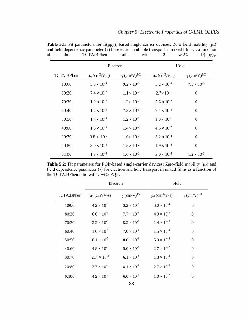
Chapter 5: Electronic Properties of G-EML OLEDs
88
Table 5.1: Fit parameters for Ir(ppy)3-based single-carrier devices: Zero-field mobility (μ0)
and field dependence parameter (γ) for electron and hole transport in mixed films as a function
of the TCTA:BPhen ratio with 2 wt.% Ir(ppy)3.
Table 5.2: Fit parameters for PQIr-based single-carrier devices: Zero-field mobility (μ0) and
field dependence parameter (γ) for electron and hole transport in mixed films as a function of
the TCTA:BPhen ratio with 7 wt% PQIr.
Electron Hole
TCTA:BPhen μ0 (cm2/V-s) γ (cm/V)1/2 μ0 (cm2/V-s) γ (cm/V)1/2
100:0 5.3 × 10⁻⁹ 9.2 × 10⁻³ 3.2 × 10⁻⁵ 7.5 × 10⁻³
80:20 7.4 × 10⁻⁷ 1.1 × 10⁻² 2.7× 10⁻³ 0
70:30 1.0 × 10⁻⁷ 1.2 × 10⁻² 5.6 × 10⁻² 0
60:40 1.4 × 10⁻³ 7.3 × 10⁻³ 9.1 × 10⁻³ 0
50:50 1.4 × 10⁻⁵ 1.2 × 10⁻² 1.0 × 10⁻¹ 0
40:60 1.6 × 10⁻⁶ 1.4 × 10⁻² 4.6 × 10⁻² 0
30:70 3.8 × 10⁻⁷ 1.6 × 10⁻² 3.2 × 10⁻⁴ 0
20:80 8.0 × 10⁻⁸ 1.5 × 10⁻² 1.9 × 10⁻⁴ 0
0:100 1.3 × 10⁻⁶ 1.6 × 10⁻² 3.0 × 10⁻⁵ 1.2 × 10⁻³
Electron Hole
TCTA:BPhen μ0 (cm2/V-s) γ (cm/V)
1/2 μ0 (cm
2/V-s) γ (cm/V)
1/2
100:0 4.2 × 10⁻⁶
3.2 × 10⁻³
3.0 × 10⁻⁴
0
80:20 6.0 × 10⁻⁶
7.7 × 10⁻³
4.9 × 10⁻³
0
70:30 2.2 × 10⁻⁶
5.2 × 10⁻³
1.4 × 10⁻³
0
60:40 1.6 × 10⁻⁴
7.0 × 10⁻³
1.5 × 10⁻²
0
50:50 8.1 × 10⁻⁵
8.0 × 10⁻³
5.9 × 10⁻⁴
0
40:60 4.8 × 10⁻³
5.0 × 10⁻³
2.7 × 10⁻²
0
30:70 2.7 × 10⁻³
6.1 × 10⁻³
1.3 × 10⁻²
0
20:80 2.7 × 10⁻⁴
8.1 × 10⁻³
2.7 × 10⁻³
0
0:100 4.2 × 10⁻²
6.0 × 10⁻³
1.0 × 10⁻²
0

Chapter 5: Electronic Properties of G-EML OLEDs
89
The high ηEQE achieved in the green and red G-EML devices is likely the result of
multiple defining characteristics of the 1:1 TCTA:BPhen gradient profile. Efficient
charge injection from the electrodes is maintained by the high composition of each
transport material near its respective electrode. Charge carrier mobilities are well-
matched at moderate compositions and remain so throughout the center region of the
device. The mobility matching over a large range of compositions, and consequently
Figure 5.6: Electron (solid symbols) and hole (open symbols) mobility for mixed films as a
function of the TCTA:BPhen composition ratio with (a) 2 wt. % Ir(ppy)3 at a field of 0.37
MV/cm and (b) 7 wt. % PQIr at a field of 0.44 MV/cm. The solid lines are guides to the eye.
10-5
10-3
10-1
Mobili
ty (
cm
2/V
s)
0.0 0.2 0.4 0.6 0.8 1.010
-7
10-5
10-3
10-1
F=0.44 MV/cm
F=0.37 MV/cm
Mobili
ty (
cm
2/V
s)
Fractional Composition BPhen
e-
h+
e-
h+
(a)
(b)

Chapter 5: Electronic Properties of G-EML OLEDs
90
throughout the 1:1 G-EML, likely leads to increased overlap between the electron and
hole charge densities in the device, allowing for efficient exciton formation. An
imbalance in the charge carrier mobility may spatially shift the exciton recombination
zone in the 2:1 and 1:1 G-EML devices, leading to a shift in the peak ηEQE (Figure 5.4a,
5.4b) with respect to applied current density. As electrons (holes) approach the anode
(cathode), the mobility decreases significantly, providing charge confinement and
reducing charge carrier leakage. Additionally, as charges are injected onto, and
transported across, their respective transport material, there exists an energy difference
between the HTM-ETM lowest unoccupied molecular orbital energy levels (for
electrons), and highest occupied molecular orbital energy levels (for holes), which
effectively confine electrons to the ETM, and holes to the HTM. The spatially-varying
composition ensures that the high concentration of transport material at the electrodes
will effectively block carriers from traveling across the entire device as leakage current, a
critical improvement over single-layer, uniformly mixed devices. The role of the
luminescent guest in charge transport was separately examined by excluding it from
single carrier device studies. For these HTM:ETM structures, the extracted charge carrier
mobilities were found to be in good agreement with the data reported here for devices
containing the HTM, ETM, and guest. Ultimately, the confluence of efficient charge
injection, large spatial overlap of the electron and hole densities, and charge and exciton
confinement results in high charge balance, with a 1:1 gradient offering the most
symmetric injection and transport conditions and thus the highest ηEQE.

Chapter 5: Electronic Properties of G-EML OLEDs
91
5.4 Optimized Blue-Light Emitting Devices
5.4.1 Performance of Blue Light-Emitting G-EML Devices
Blue G-EML OLEDs with 2:1, 1:1, and 1:2 gradient profiles were fabricated
using the methods described previously. The resulting dependence of ηEQE on applied
current density is shown in Figure 5.7 for each gradient. A strong dependence on
gradient profile is observed, with the 1:2 G-EML device showing peak performance.
The charge carrier mobilities were extracted by fitting single carrier current density-
electric field curves for uniform mixtures of varying composition using Eqns. 5.1 and 5.2.
Selected electron- and hole-only data and the associated fits are shown in Figures. 5.8a
and 5.8b, respectively, with the corresponding μ0 and γ values listed in Table 5.3. The
carrier mobility at an applied field equivalent to the peak in ηEQE (0.30 MV/cm) for a 1:2
G-EML is shown versus TPBi composition in Figure 5.9. In contrast to the TCTA:BPhen
material system, the TCTA:TPBi material system shows charge carrier mobilities which
Figure 5.7: External quantum efficiency versus current density for FIrpic-based G-EML
devices with varying overall HTM:ETM composition.
10-3
10-2
10-1
100
101
102
103
104
0
2
4
6
8
10
12
2:1
1:1
1:2
E
QE
(%)
Current Density (mA/cm2)

Chapter 5: Electronic Properties of G-EML OLEDs
92
are mismatched over a wide range of host compositions. Additionally, no significant
decrease is observed for the hole mobility in TPBi-rich devices. TPBi doped with 4 wt.%
FIrpic transports holes with a mobility similar to that of TCTA:FIrpic. The lack of a roll-
off in hole mobility versus TPBi composition, and thus also position in the G-EML
device, may allow for increased hole leakage. The spatial overlap of the electron and
hole densities in the 2:1 and 1:1 G-EMLs is likely small due to the low electron mobility
in TCTA-rich devices. This likely forces the exciton recombination zone towards the
cathode, potentially resulting in additional metal-quenching losses.133,134
Figure 5.8: Current density-voltage characteristics for 100:0 TCTA:TPBi (squares), 50:50
TCTA:TPBi (diamonds), and 0:100 TCTA:TPBi (triangles) (a) electron-only and (b) hole-
only single-carrier devices with 4 wt.% FIrpic. Symbols represent measured data while solid
lines are fits to Eqns. 5.1 and 5.2.
10-10
10-8
10-6
10-4
10-2
100
100:0
50:50
0:50
Curr
ent
Density (
mA
/cm
2)
0 500000 100000010
-9
10-7
10-5
10-3
10-1
Curr
ent
Density (
mA
/cm
2)
Electric Field (V/cm)
100:0
50:50
0:100
(a)
(b)

Chapter 5: Electronic Properties of G-EML OLEDs
93
Figure 5.9: Electron (solid symbols) and hole (open symbols) mobility at a field F = 0.30
MV/cm for mixed as a function of the TCTA:TPBi composition ratio with 4 wt. % FIrpic.
The solid lines are guides to the eye.
0.0 0.2 0.4 0.6 0.8 1.010
-8
10-6
10-4
10-2
100
Mobili
ty (
cm
2/V
s)
Fractional Composition TPBi
e-
F=0.3 MV/cm
h+
Table 5.3: Fit parameters for FIrpic-based single-carrier devices: Zero-field mobility (μ0) and
field dependence parameter (γ) for electron and hole transport in mixed films as a function of
the TCTA:TPBi ratio with 4 wt% FIrpic.
Electron Hole
TCTA:TPBi μ0 (cm2/V-s) γ (cm/V)
1/2 μ0 (cm
2/V-s) γ (cm/V)
1/2
100:0 1.0 × 10⁻⁸
4.0 × 10⁻³
1.2 × 10⁻⁴
1.8 × 10⁻³
80:20 7.6 × 10⁻⁸
4.3 × 10⁻³
2.8× 10⁻³
0
70:30 2.0 × 10⁻⁶
3.3 × 10⁻³
4.4 × 10⁻³
0
60:40 1.3 × 10⁻⁵
2.5 × 10⁻³
3.0 × 10⁻³
0
50:50 4.9 × 10⁻⁵
2.5 × 10⁻³
7.4 × 10⁻³
0
40:60 3.1 × 10⁻⁷
6.0 × 10⁻³
6.8 × 10⁻³
0
30:70 1.4 × 10⁻⁶
5.0 × 10⁻³
7.7 × 10⁻³
0
20:80 1.2 × 10⁻⁴
6.0 × 10⁻³
1.2 × 10⁻²
0
0:100 2.5 × 10⁻³
7.0 × 10⁻³
1.9 × 10⁻²
0

Chapter 5: Electronic Properties of G-EML OLEDs
94
In a 1:2 G-EML, a large region of the device is TPBi-rich. As the electron
mobility is highest for ETM-rich compositions, the 1:2 device offers a larger spatial
extent where both the electron and hole mobilities are maximized. The electron density
is thus extended further into the device, improving charge balance and exciton formation.
The improved charge balance leads to an enhancement in both ηEQE and ηP. In an ideal
G-EML device, electron and hole mobilities would be matched over a wide range of
compositions, falling only at extreme compositions to aid charge confinement. An ETM
with a higher mobility, or conversely, an HTM with a slightly lower mobility, would
likely lead to improved charge balance and efficiency in blue-emitting G-EML devices.
5.5 Flexible Transistor-Driven G-EML OLEDs
The high-efficiency, low-voltage characteristics of the devices above, together
with their simple construction, make the red-, green-, and blue-emitting G-EML OLEDs
attractive for use in fully flexible displays applications. For active-matrix OLED
(AMOLED) displays, this requires integration of the OLED pixel with fully flexible thin-
film transistor (TFT) drive circuitry. To maintain compatibility with flexible polymer
substrates, both the TFTs and OLEDs must be processed at low temperature. Thus,
organic electrolyte-gated transistors, which may be fabricated at room temperature, are an
attractive solution.135
5.5.1 Organic Electrolyte-Gated Transistors
Organic electrolyte-gated transistors (OETs) are microelectrochemical transistors
which have been shown to achieve high transconductances (~10 mS cm-1
) with low gate

Chapter 5: Electronic Properties of G-EML OLEDs
95
voltage biases.135
A schematic of an aerosol jet printed OET is shown in Figure 5.10a
with the constituent materials in Figure 5.10b and 5.10c. This device utilizes a room
temperature ionic liquid, (1-ethyl-3- methylimidazolium
bis(trifluoromethylsulfonyl)imide) “[EMIM][TFSI]” in a gelating triblock copolymer
(poly(styrene-b-methylmethacrylate-b-styrene) “PS-PMMA-PS” as the flexible ion gel
gate dielectric and poly(3-hexylthiophene) “P3HT” as the semiconducting channel.
When a negative bias is applied to the gate electrode, ions penetrate the semiconducting
layer, oxidizing it and creating a high conductance channel between the source and drain
electrodes. At the same time, part of the poly(3,4-ethylenedioxythiophene)
Figure 5.10: (a) Cross section of a printed organic thin film electrochemical transistor (OET).
When a negative gate voltage is applied, the semiconductor is electrochemically doped by
anions from the electrolyte and a high conductance state is created in the transistor active
layer. (b) Molecular structure of the employed electrolyte-dielectric and (c) semiconductor
(P3HT). The ion-gel dielectric is a solid electronic insulator made by a gelating triblock
copolymer (PS-PMMA-PS) swollen with an ionic liquid ([EMIM][TFSI]).

Chapter 5: Electronic Properties of G-EML OLEDs
96
poly(styrenesulfonate) (PEDOT:PSS) gate electrode is reduced to a lower conductance
state. Unwanted effects related to the decrease of the PEDOT:PSS conductance are
avoided by employing a highly conductive PEDOT:PSS electrode exceeding the channel
layer in thickness and lateral dimension.
Figure 5.11 displays the quasi-equilibrium transfer characteristics of an OET in
the linear (VD = - 0.1 V) and saturation (VD = - 1.5 V) regimes. Unique features of this
device are a high p-type transconductance, low hysteresis, low sub-threshold voltage
slope and low turn-on voltage (VON ~ 0 V). Moreover, the transistors are reasonably
stable under gate voltage stress136
and there is good uniformity between the
characteristics of different devices printed on the same substrate.135,137
These properties,
together with the low parasitic resistance at the injecting/extracting contacts138
and the
Figure 5.11: Quasi-equilibrium transfer characteristics of a gel-electrolyte gated organic
transistor in linear (VD = -0.1 V) and saturation (VD = -1.5 V) regimes (sweep rate = 50 mV/s).
Transistor channel length (L) and width (W) are L = 10 μm and W = 100 μm, respectively.
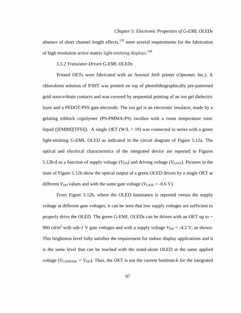
Chapter 5: Electronic Properties of G-EML OLEDs
97
absence of short channel length effects,139
meet several requirements for the fabrication
of high resolution active matrix light-emitting displays.140
5.5.2 Transistor-Driven G-EML OLEDs
Printed OETs were fabricated with an Aerosol Jet® printer (Optomec Inc.). A
chloroform solution of P3HT was printed on top of photolithographically pre-patterned
gold source/drain contacts and was covered by sequential printing of an ion gel dielectric
layer and a PEDOT:PSS gate electrode. The ion gel is an electronic insulator, made by a
gelating triblock copolymer (PS-PMMA-PS) swollen with a room temperature ionic
liquid ([EMIM][TFSI]). A single OET (W/L = 10) was connected in series with a green
light-emitting G-EML OLED as indicated in the circuit diagram of Figure 5.12a. The
optical and electrical characteristics of the integrated device are reported in Figures
5.12b-d as a function of supply voltage (VDD) and driving voltage (VGATE). Pictures in the
inset of Figure 5.12b show the optical output of a green OLED driven by a single OET at
different VDD values and with the same gate voltage (VGATE = -0.6 V).
From Figure 5.12b, where the OLED luminance is reported versus the supply
voltage at different gate voltages, it can be seen that low supply voltages are sufficient to
properly drive the OLED. The green G-EML OLEDs can be driven with an OET up to ~
900 cd/m2
with sub-1 V gate voltages and with a supply voltage VDD = -4.2 V, as shown.
This brightness level fully satisfies the requirement for indoor display applications and it
is the same level that can be reached with the stand-alone OLED at the same applied
voltage (VCATHODE = VDD). Thus, the OET is not the current bottleneck for the integrated

Chapter 5: Electronic Properties of G-EML OLEDs
98
device. Indeed, by comparing Figure 5.12b with the luminance-voltage characteristics of
the stand-alone diode, it can be seen that when the transistor is fully-ON (VGATE = -0.6 V)
there are no differences between the luminance vs. supply voltage response of the stand-
alone OLED and the integrated device.
Figures 5.12c and 5.12d show the dependence of luminance and OLED current
density on gate voltage for different fixed VDD values. When the driving transistor is
gated with low negative or positive biases, the OLED brightness is significantly
suppressed, as expected, Figure 5.12c. The limit of zero light emission is achieved when
the gate electrode is grounded, and maintained when a low positive gate bias is applied.
Figure 5.12: Optical and electrical characteristics of an OET/OLED integrated device using a
green G-EML OLED. (a) Circuit diagram showing the driver TFT in series with the light-
emitting unit. (b) Luminance vs. supply voltage (VDD) at different gate voltages (VGATE) and (c)
luminance vs. gate voltage at different VDD. (d) Current density at the OLED cathode versus
VGATE for different VDD . Transistor channel length and channel width are L = 20 μm and W =
200 μm, respectively. In the inset of Figure 3 (b) pictures of the light-emitting unit at different
brightness are also reported.

Chapter 5: Electronic Properties of G-EML OLEDs
99
A sharp increase in the luminance is observed when the gate voltage is swept negatively
with VDD > -3 V. Indeed, the OET turns ON abruptly, because of the extremely low sub-
threshold swing, and properly drives the light-emitting unit at gate voltages smaller than -
1 V. At sufficiently high VGATE the OLED luminance saturates to the maximum
brightness of the stand-alone OLED at VCATHODE = VDD. The OLED current density also
saturates and follows the same trend as the luminance data (compare Figures 5.12c and
5.12d). In this case, the optical responses of the stand-alone OLED and of the integrated
device are exactly the same and the output current of the transistor exceeds what is
required to drive the diode at the given supply voltage. In other words, the saturation of
the luminance versus VGATE characteristics and current density versus VGATE
characteristics in Figure 5.12c and Figure 5.12d indicate that the OLED, and not the
OET, limits the current, as is desired.
5.5.3 Dynamic Response of OET-Driven G-EML OLEDs
After characterization of integrated OET/OLED devices in the quasi-equilibrium
regime, the response to a dynamic gate bias was examined. The driver TFT was gated
with a square wave-function (0 < VGATE < -0.64 V) at different frequencies, while a
constant supply bias VDD = -4.2 V was applied between the transistor source and the
diode cathode. Consequently, the output of the OLED was modulated in time. In Figure
5.13a and Figure 5.13b the optical output of a green OLED and the voltage signal applied
to the gate of the driving TFT is reported versus time. The gate modulating signal was a
square wave-function at 10 Hz (Figure 5.13a) and 100 Hz (Figure 5.13b), respectively. At

Chapter 5: Electronic Properties of G-EML OLEDs
100
10 Hz the OLED emission closely follows the gate signal, switching from a maximum
value of ~900 cd/m2 (ON-transistor at VGATE = -0.64 V) to ~ 0 cd/m
2 (OFF-transistor at
VGATE = 0 V). Similar behaviour is observed when signals with frequencies up to 60 Hz
are employed. However, as the frequency increases to 100 Hz, the OLED contrast
decreases. The integrated device still responds quickly to the gate signal, but a substantial
increase of the OLED brightness during the transistor OFF-state is observed (Figure
5.13b). Indeed, at high switching frequencies, the OET can still provide enough current to
properly drive the OLED, but the device leakage current increases so that the OLED light
emission cannot be completely suppressed. The increase of the leakage current is due to
less effective electrochemical dedoping of the semiconductor at high switching
Figure 5.13: Optical response of an OET/OLED integrated device under dynamic operation.
(a) Luminance and driving TFT gate voltage vs. time at 10 Hz and (b) luminance and TFT
gate voltage vs. time at 100 Hz. In both cases the constant supply voltage is VDD = -4.2 V. (c)
Gate stress measurement on an integrated device at switching frequency of 10 Hz and at a
constant supply voltage VDD = -4 V. The upper and the lower panels report the applied gate
voltage and the device optical output versus time, respectively.

Chapter 5: Electronic Properties of G-EML OLEDs
101
frequencies (reduced ion diffusion from the channel into the dielectric),136
and to the
contribution of the capacitive current. These effects could be minimized by further
optimizing the printing process (giving thinner semiconducting and electrolyte-dielectric
layers) and by reducing the dimensions of the source/drain electrodes.
In Figure 5.13c the stability of the integrated devices under dynamic operation is
reported. A green OLED was driven by a single OET at a gate switching frequency of 10
Hz and at constant supply voltage VDD = -4 V. This is the VDD at which luminance
suitable for display applications (~ 500 cd/m2) can be achieved with these devices. In
order to clearly detect degradations of the device efficiency, the driving transistor was
gated at low voltage (VGATE = -0.6 V), e.g., close to the voltage edge at which saturation
of the driving current occurs. The gate voltage and the luminance of the OLED are
reported versus time in the upper and lower panel of Figure 5.13c, respectively. The
integrated device is reasonably stable under bias stress conditions and that after two hours
of dynamic operation the diode optical output still follows properly the gate modulation.
Indeed, there are no remarkable changes in the falling and rising edges of the optical
signal or in the brightness level of the device OFF-state. However, during the stressing
period there is a ~20 % decrease of the maximum OLED luminance. This can be
attributed to degradation of both the driving TFT (shift of the threshold voltage and
decrease of the total output current) and of the OLED.

Chapter 5: Electronic Properties of G-EML OLEDs
102
5.6 Conclusions
Efficient green, red, and blue OLEDs have been demonstrated which consist of a
single, engineered organic layer. The devices exhibit high ηEQE and ηP owing to the high
charge balance, low-voltage, and tunability of the G-EML device structure. Indeed, the
low-voltage, high-efficiency operation of the G-EML OLED allows integration with fully
flexible organic thin-film transistors. Together, the integrated devices are able to produce
display and lighting relevant brightness levels, even under dynamic modulation, while
maintaining compatibility with flexible substrates.
Single-carrier devices are used to extract the field-dependent charge carrier
mobilities over a range of HTM:ETM:Guest compositions. The dependence of the
electron and hole mobilities on composition, and thus position, is found to strongly
influence device operation and performance. The optimal gradient profile is one which
both maximizes and balances the electron and hole mobilities, achieving carrier and
exciton confinement and large spatial overlap of electron and hole densities. The G-EML
device structure is able to overcome a mismatch in HTM and ETM mobilities through
careful tuning of the gradient profile, and thus may be a powerful tool in realizing
simplified, high-efficiency OLEDs using a range of active materials.
5.7 Acknowledgements
This work was done in collaboration with Daniele Braga and C. D. Frisbie from
the department of Chemical Engineering and Materials Science at the University of

Chapter 5: Electronic Properties of G-EML OLEDs
103
Minnesota (UMN). Keun Hyung Lee (UMN) prepared the PS-PMMA-PS used in the
organic electrochemical transistors.

Chapter 6: Measurement of the Recombination Zone of Organic Light-Emitting Devices
104
Chapter 6 - Measurement of the Recombination Zone of Organic
Light-Emitting Devices
In phosphorescent OLEDs, high external quantum efficiencies (ηEQE) have been
realized using a variety of device architectures with varying degrees of
complexity.13,25,61,80,88,89,99,107,113,141,142
As understanding of the fundamental processes
relevant for efficient device operation has improved, models of the optical and electronic
characteristics of multilayer devices have become increasingly predictive.27,143,144
One
important feature of OLEDs which has proven difficult to probe experimentally is the
spatial extent and location of the exciton recombination zone.143
The spatial overlap
between the exciton density and the local optical field greatly impacts the efficiency with
which photons escape the device,74,145,146
as well as the intrinsic radiative decay rate of
the exciton.143,147–149
The spatial extent of recombination has also been identified as an
important parameter that governs the degree to which the ηEQE decreases under high
excitation,14,15,129
termed the efficiency “roll-off.” The mechanisms responsible for the
roll-off are separated into two general categories: a reduction in confinement in the
emissive layer and bimolecular exciton quenching. The reduction in confinement at high
drive current densities reduces the fraction of injected carriers which form excitons, and
can be an obstacle to high efficiency operation.129
However, such losses can often be
mitigated through the use of charge carrier blocking layers that confine injected electrons
and holes to the emissive layer. In terms of the bimolecular quenching of excitons, it is
understood that in systems which employ long-lifetime phosphorescent emitters, triplet-
Chapter 6: Measurement of the Recombination Zone of Organic Light-Emitting Devices
105
triplet annihilation (TTA) and triplet-polaron quenching (TPQ) are the dominant
mechanisms for roll-off at device-relevant electric fields, both of which are strongly
dependent on the local density of excitons.14,15,129–131,150–152
As already noted, to achieve high peak ηEQE in an OLED effective exciton
confinement is required in the emissive layer. This is often realized through the use of
charge and exciton blocking layers with specific properties, including a shallow lowest
unoccupied molecular orbital (LUMO) energy level to block electrons, a deep highest
occupied molecular orbital (HOMO) energy level to block holes, or a large energy gap to
confine excitons to the emissive layer. One challenge in multilayer devices which
incorporate blocking layers is achieving balanced electron and hole injection into the
emissive layer. Differences in the barrier heights and charge carrier mobilities for the
electron and hole transport pathways inevitably lead to an emissive layer with an excess
of one carrier type.144
Additionally, the mobilities of electrons and holes often show
different field dependencies,98,115,126
further complicating charge balance across the useful
range of drive voltages. As a result of this relative charge imbalance in the emissive
layer, the recombination zone is likely pinned at the interface between the emissive layer
and the minority carrier transport layer. In the absence of substantial exciton diffusion or
significant exciton quenching effects, the recombination zone is equivalent to the exciton
generation profile, and is determined by the spatial overlap of the electron and hole
charge densities in the emissive layer.

Chapter 6: Measurement of the Recombination Zone of Organic Light-Emitting Devices
106
Device architectures which have shown improved charge balance and charge and
exciton confinement often incorporate a double-emissive layer (D-EML) or mixed-
emissive layer (M-EML).80,81,87–89,103
The D-EML consists of two distinct layers, a hole-
transport material (HTM) and an electron transport material (ETM), with an emissive
guest uniformly doped throughout both layers. This design strongly confines the charge
carriers to a region near the HTM:ETM interface.80
The M-EML design consists of a
uniformly mixed layer of HTM and ETM that is doped with a luminescent guest. This
design has a large interfacial area between HTM and ETM to facilitate exciton formation
and the charge carrier mobilities can be tuned by varying the ratio of HTM:ETM.98,112,115
Both architectures are usually incorporated into multilayer structures to realize effective
charge and exciton confinement.89,111
6.1 Conventional Methods to Measure the Recombination Zone
Conventional experimental determinations of the recombination zone in an OLED
have focused on two techniques: translating the position of the guest emitter across the
emissive layer while observing large changes in device performance, or monitoring the
shape of the emission profile versus viewing angle and deducing the location of exciton
generation based on weak microcavity effects.85,98,153–157
While the former technique may
give a qualitative determination of the recombination zone location, it gives little
information about the recombination zone width and it neglects the often significant role
played by the emissive guest in charge transport or charge injection into the emissive
layer. This effect may be quite large, especially in devices which employ a single

Chapter 6: Measurement of the Recombination Zone of Organic Light-Emitting Devices
107
emissive layer where the host preferentially carries one type of charge, or use large
doping concentrations where the guest may participate in charge transport.69,85,158
The
latter technique compares measured data to fits of optical models and is limited by
assumptions present in the optical model.156
A third technique which has recently been
discussed employs a strip-doping method which relies on nearest-neighbor exciton
quenching methods.15,159
Use of this technique requires a high local concentration of a
quenching molecule, which may impact the electrical properties of the emissive layer.
6.2 Sensing Excitons with Energy Transfer
In this work, the exciton recombination zone in OLEDs with various emissive
layer architectures is probed directly through the addition of a fluorescent sensitizer,
capable of quenching excitons formed on the emissive guest, at different locations within
the emissive layer. By comparing the overall emission intensity of sensitized devices to
control structures containing no sensitizer, a ‘map’ of the local exciton density may be
determined. Electrical measurements are performed to ensure that the inclusion of the
sensitizer does not alter the electrical characteristics of the devices. This technique is
applied to simplified OLEDs containing common emissive layer architectures, namely D-
EML and M-EML-type structures, as well as an OLED based on a graded-emissive layer
(G-EML), shown schematically in Figures 6.1a-c. The simplified structures facilitate
comparisons of the recombination zones in the different devices and show the influence
of emissive layer architecture on the recombination zone. The G-EML device offers an
architecture which contains no sharp interfaces between HTM and ETM host layers or
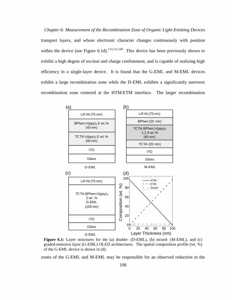
Chapter 6: Measurement of the Recombination Zone of Organic Light-Emitting Devices
108
transport layers, and whose electronic character changes continuously with position
within the device (see Figure 6.1d).113,115,160
This device has been previously shown to
exhibit a high degree of exciton and charge confinement, and is capable of realizing high
efficiency in a single-layer device. It is found that the G-EML and M-EML devices
exhibit a large recombination zone while the D-EML exhibits a significantly narrower
recombination zone centered at the HTM:ETM interface. The larger recombination
zones of the G-EML and M-EML may be responsible for an observed reduction in the
Figure 6.1: Layer structures for the (a) double- (D-EML), (b) mixed- (M-EML), and (c)
graded-emissive layer (G-EML) OLED architectures. The spatial composition profile (wt. %)
of the G-EML device is shown in (d).
0 20 40 60 80 1000
20
40
60
80
100 HTM
ETM
Guest
Com
positio
n (
wt.
%)
Layer Thickness (nm)
TCTA:Ir(ppy)3 5 wt.%
(40 nm)
ITO
Glass
LiF/Al (75 nm)
BPhen:Ir(ppy)3 5 wt.%
(40 nm)
D-EML
TCTA:BPhen:Ir(ppy)3
1:1:5 wt.%
(60 nm)
ITO
Glass
LiF/Al (75 nm)
TCTA (20 nm)
BPhen (20 nm)
M-EML
TCTA:BPhen:Ir(ppy)3
2 wt. %
G-EML
(100 nm)
ITO
Glass
LiF/Al (75 nm)
G-EML
(a)
(c)
(b)
(d)

Chapter 6: Measurement of the Recombination Zone of Organic Light-Emitting Devices
109
efficiency roll-off compared to devices containing a D-EML. The efficiency roll-off is
considered in greater detail in Chapter 7.
6.2.1 Theory of Exciton Sensitization
Any technique designed to give a quantitative measurement of the exciton
recombination zone requires: (i) a high sensitivity to the presence of guest excitons, (ii) a
high degree of spatial resolution, and (iii) that it must not substantially alter the natural
distribution of charge carriers or excitons within the device. One way to sense the
recombination zone is by locally transferring excitons formed on the emissive guest to a
second, “sensitizing” molecule.15
Once the exciton is transferred from the guest to the
sensitizer, it may be detected by monitoring emission from the sensitizer, or by selecting
a sensitizing material which does not readily luminesce. In the later case the guest
exciton is effectively quenched by the sensitizer, resulting in a measurable reduction in
luminescence from the guest. Depending on the guest and sensitizing materials,
quenching may occur via Dexter- or Förster-type energy transfer.1,9
Quenching via
Dexter energy transfer requires a physical exchange of electrons between the guest and
sensitizer and is therefore a nearest-neighbor process. The rate of Dexter energy transfer
falls off steeply with increasing separation between guest and sensitizer molecules.9
While this mechanism may be a highly localized process, satisfying condition (ii), it
requires a high density of sensitizer molecules in order to ensure that the sensitizer is
adjacent to the dilute-doped guest, likely influencing the local electronic environment.15
Förster energy transfer is a non-radiative dipole-dipole coupling between a donor (i.e.

Chapter 6: Measurement of the Recombination Zone of Organic Light-Emitting Devices
110
guest) and acceptor (i.e. sensitizer) molecule. This interaction may occur through
occupied space, extending the range of energy transfer and quenching. The rate of
Förster energy transfer between point dipoles is given by:26
[ ]
(
)
, (6.1)
where τ is the exciton lifetime, d is the donor-acceptor molecular separation, and R0 is the
characteristic radius of Förster energy transfer, given by:9,26
∫ [ ] [ ] , (6.2)
where ηPL is the photoluminescence efficiency of the donor, κ is the dipole orientation
factor, n is the index of refraction of the medium between the donor and acceptor, λ is the
wavelength, FD is the area-normalized donor emission spectrum, and σA is the absorption
cross-section of the acceptor. Förster energy transfer between the guest and sensitizer,
and thus the spatial resolution of exciton quenching, may be tuned by selecting a
sensitizing material with an appropriate overlap of absorption with the guest emission.
Quenching may then occur over a small distance (~1-5 nm) and retain a high sensitivity
to the presence of guest excitons, allowing a low sensitizer concentration to be used (<1
wt.%). Such a low doping concentration is unlikely to affect charge transport and leads
to only a slight reduction in spatial resolution.
In this chapter, a measurement of the recombination zone in a variety of common
emissive layer architectures is realized by including a highly localized, lightly-doped strip
of tetraphenyltetrabenzoporphyrin (TPTBP) into a device to quench excitons formed on
the luminescent guest via Förster energy transfer. The composition of the sensitized strip

Chapter 6: Measurement of the Recombination Zone of Organic Light-Emitting Devices
111
is otherwise matched to the local concentrations of the host and guest materials for a
particular structure. Here, TPTBP is selected based on the small overlap of its absorption
cross section with the photoluminescence (PL) of the archetypical green phosphor, tris(2-
phenylpyridine)iridium(III) (Ir(ppy)3) (see Figure 6.2a). In a separate measurement,
TPTBP showed extremely weak luminescence under electrical excitation, this ensures
that excitons transferred from Ir(ppy)3 predominantly decay non-radiatively. Subsequent
measurements of the electroluminescence (EL) from sensitized devices
containing both TPTBP and Ir(ppy)3 showed no observable contribution from TPTBP.
Figure 6.2: (a) Extinction coefficient for the sensitizer, TPTBP, (dashed line) and peak-
normalized electroluminescence (EL) spectrum of the emissive guest, Ir(ppy)3 (solid line).
Inset: Molecular structure of TPTBP. (b) Schematic representation of the sensitizing strip
technique.
450 500 550 600 650 7000.0
0.2
0.4
0.6
0.8
0.0
0.2
0.4
0.6
0.8
1.0
Extin
ctio
n C
oeff
icie
nt
Wavelength (nm)
EL
Inte
nsity
(a. u
.)
(a)
(b)
Ca
thod
e
Anode
Gla
ss
D-EML, M-EML, or G-EML Emissive Layer
Sensitized Strip
- Guest Emitter
- SensitizerHost Matrix
TPTBP

Chapter 6: Measurement of the Recombination Zone of Organic Light-Emitting Devices
112
Using Eqn. 6.2 and the optical properties of TPTBP and Ir(ppy)3, an R0 = 3.9 nm is
calculated. The Förster quenching distance, and thus the spatial resolution of the
measurement, may be tuned by selecting a sensitizer with a small overlap of absorption
with guest emission, ensuring a small R0 and high degree of spatial resolution. The
integrated EL intensity of each sensitized device is measured and compared to a control
device which does not contain TPTBP, this quantity is termed the “EL ratio” ≡ β. This
ratio is directly proportional to the ratio of quenched excitons and therefore the quantity
1-β is proportional to the ratio of unquenched excitons, i.e. the local exciton density. A
map of the recombination zone is realized by fabricating a series of devices with the
sensitizing strip translated throughout the emissive layer, and plotting the local exciton
density versus strip position (Figure 6.2b). One factor that is not included but may
become important in wide-recombination zone devices is the spatial dependence of the
far-field extraction efficiency of excitons at different positions within the EML. The
optical field properties, and the effects of optical field on OLEDs, are discussed further in
Chapter 8.
6.2.2 Theory of the Electronic Model of G-EML OLEDs
Theoretical models for the spatial charge density in an organic semiconductor
have previously been developed for multilayer OLEDs.27,144,161
To describe the
environment of a single-layer, G-EML device (Figure 6.1c), we adapt a model from
Neumann et al.162
which considers charge carrier drift, diffusion, and recombination to
describe charge densities and the recombination zone. It is important to note that the

Chapter 6: Measurement of the Recombination Zone of Organic Light-Emitting Devices
113
charge densities, electric field, and mobility are all position dependent in a G-EML,115
thus we have chosen to make this explicit by including [x] in all subsequent, spatially-
dependent equations.
The one-dimensional equations are:
[ ]
[ ] [ ] , (6.3)
[ ] [ ] , (6.4)
[ ] [ ] , (6.5)
where Eqn. 6.3 is Poisson’s equation. Here, F[x] is the electric field, e is the elementary
charge, ε is the relative permittivity of the organic layer (taken here as ε = 3), ε0 is the
permittivity of vacuum, p[x] is the hole density, and n[x] is the electron density. The
continuity equations for electrons and holes are given in Eqns. 6.4 and 6.5, respectively,
and contain a Langevin-type recombination term. Langevin recombination has been
extensively used to describe recombination in OLEDs.1,163,164
In this formalism, γ is the
recombination coefficient:
[ ] [ ] . (6.6)
The electron current density is given by:
[ ] [ ] [ ] [ ] [ ]
(6.7)
and contains a field-dependent drift term as well as a diffusion term. Similarly, the hole
current density is given by:
[ ] [ ] [ ] [ ] [ ]
. (6.8)

Chapter 6: Measurement of the Recombination Zone of Organic Light-Emitting Devices
114
In these expressions we have assumed the validity of the Einstein relation relating the
drift and diffusion of charge. To simplify the evaluation of the continuity equations,
dimensionless quantities are used to describe the position, the electric field, and the
charge densities:
, (6.9)
[ ]
[ ], (6.10)
[ ] [X]
, (6.11)
[ ] [ ]
, (6.12)
where L is the width of the G-EML layer and V is the applied voltage. Using the
continuity equations and the electron and hole current densities defined in Eqns. 6.3-6.8,
together with the dimensionless variables defined above, we derive four steady-state,
coupled equations for the voltage, electric field and the carrier densities:
[ ] [ ]
, (6.13)
[ ] [ ] [ ], (6.14)
[ ] [ ] [ ] [ ]
[ ] [ ]
[ ]
[ ]
[ ]
[ ]
[ ]
[ ] [ ] [ ]
[ ] (6.15)
[ ] [ ] [ ] [ ]
[ ] [ ]
[ ]
[ ]
[ ]
[ ]
[ ]
[ ] [ ] [ ]
[ ]
[ ]. (6.16)

Chapter 6: Measurement of the Recombination Zone of Organic Light-Emitting Devices
115
While it is possible to write Poisson’s equation in terms of V directly, it is instructive to
solve for the shape of the field (as determined by N[X] and P[X]) while using V to set the
boundary conditions. This matches well with actual device operation, where a potential
is applied to the electrodes and the field may vary depending on the local electron and
hole charge densities. The boundary conditions imposed are:
[ ] [ ] (6.17)
[ ] [ ] (6.18)
[ ] (6.19)
[ ] (6.20)
The boundary conditions in Eqn. 6.17 constrain the system such that there is no electron
leakage to the anode, no hole leakage to the cathode, and all current comes from the
recombination of carriers. This scenario is valid given the high efficiencies obtained in
Chapter 3 for single-layer G-EML OLEDs. Together with the boundary conditions of
Eqn. 6.18, an equal number of holes and electrons are present in the device. This last
constraint ensures that the model reflects the steady-state behavior of the device and can
be confirmed by comparing the integrated charge densities. The boundary conditions of
Eqns. 6.19 and 6.20 reflect a system where one side is grounded and a potential is applied
at the opposite side. The magnitude of the applied voltage is varied in the coupled
equations. Finally, the product of the electron (N[X]) and hole (P[X]) charge densities
(the ‘NP product’) is equivalent to the exciton density profile, and thus reflects the extent
of the exciton recombination zone with exciton diffusion assumed to be negligible. This

Chapter 6: Measurement of the Recombination Zone of Organic Light-Emitting Devices
116
last assumption is valid for cases where the exciton is well-confined to the guest and the
guest concentration is low, both of which are typical conditions in an OLED.
6.3 Experimental Methods
The Förster radius was calculated using the extinction coefficient of TPTBP as
measured by spectroscopic ellipsometery, the PL spectrum of Ir(ppy)3, an average index
of refraction (n = 1.8) for the TCTA:BPhen host at the peak in Ir(ppy)3 emission as
determined by spectroscopic ellipsometery, and the photoluminescence quantum yield of
Ir(ppy)3, taken as ηPL = 95% based on previous work.24
The formula weight of TPTBP is
816.99 g mol-1
and a density 1.2 g cm-1
was measured via X-ray reflectivity. Using Eqn.
6.2 and the above parameters, a Förster radius of R0 = 3.9 nm is calculated. The Förster
radius is primarily determined by the overlap of sensitizer absorption cross-section with
the guest PL.
All devices are fabricated by the vacuum thermal evaporation methods described
in Chapter 2. Green-emitting devices were fabricated using 4,4',4''-tris(carbazol-9-
yl)triphenylamine (TCTA) and 4,7-diphenyl-1,10-phenanthroline (BPhen) as the HTM
and ETM, respectively, with Ir(ppy)3 as the luminescent guest and TPTBP (Frontier
Scientific) as the quencher in sensitized devices; all materials were used as received. All
organic layers were deposited in high vacuum (<10-7
Torr) with independent quartz
crystal monitors measuring the deposition rate of each material, allowing for careful
control of the concentration and location of TPTBP within the devices. The G-EML
devices were fabricated using time-varying deposition rates as described previously, with

Chapter 6: Measurement of the Recombination Zone of Organic Light-Emitting Devices
117
an optimal Ir(ppy)3 doping concentration of 2 wt.%. Sensitized G-EML devices included
a 4-nm-thick strip of 1 wt. % TPTBP with concentrations of TCTA, BPhen and Ir(ppy)3
that are matched to the spatial location of the strip. The D-EML and M-EML devices
were fabricated using the following optimized structures: ITO/40 nm TCTA:Ir(ppy)3 (5
wt.%)/40 nm BPhen:Ir(ppy)3 (5 wt.%) for the D-EML, and ITO/20 nm TCTA/60nm
TCTA:BPhen:Ir(ppy)3 (1:1:5 wt.%)/20 nm BPhen for the M-EML. The additional TCTA
and BPhen layers present in the M-EML device serve to confine charge the emissive
layer; M-EML devices fabricated without such blocking layers have large leakage
currents and show poor device performance. Sensitized M-EML devices contained a 4-
nm-thick strip of 1 wt.% TPTBP and D-EML devices contained a 2-nm-thick strip of 1
wt.% TPTBP with concentrations of TCTA, BPhen, and Ir(ppy)3 corresponding to the
spatial location within each device. The ratio of the strip width to measured
recombination zone width remains <10% in all device architectures, ensuring a high
degree of spatial accuracy
6.4 Measurements of the Exciton Recombination Zone
The current density-voltage (J-V) characteristics for selected sensitized devices
are shown in Figures 6.3a-c for D-EML, M-EML, and G-EML devices, respectively, as a
function of strip position, along with control devices that do not contain the sensitizing
strip. To ensure that variations in the J-V characteristics are not strip-position dependent
and are instead the result of minor sample-to-sample variations, the current density of
each sensitized device at 5 V is plotted versus strip position in Figures 6.3d-f for D-EML,

Chapter 6: Measurement of the Recombination Zone of Organic Light-Emitting Devices
118
M-EML, and G-EML devices, respectively. The error bars are taken as the device-to-
device variation observed for control devices fabricated in different runs. For each of the
architectures, differences in the current densities do not trend systematically with
sensitizer position, suggesting that the inclusion of the doped sensitizing strip does not
substantially impact charge transport, satisfying condition (iii) discussed previously.
The measured exciton recombination zone for a D-EML device is shown in
Figure 6.4a at an applied current density of 10 mA cm-2
and is found to be pinned at the
Figure 6.3: Current density-voltage characteristics (J-V) for (a) D-EML, (b) M-EML, and (c)
G-EML devices with a sensitizing strip located at different positions within the emissive layer
(as measured from anode, in the case of the D-EML and G-EML, or from the TCTA/M-EML
interface, for M-EML devices). Data for devices with intermediate strip positions are omitted
for clarity. A control device which does not contain the sensitizing strip is shown (closed
symbols) for each of the device architectures of interest. The current density at an applied
voltage of 5 V for each device is shown in (d) for D-EML devices, (e) for M-EML devices,
and (f) for G-EML devices; the horizontal line represents the average current density of the
devices and error bars are calculated from the current density variation of control devices
fabricated in different runs.
0.1 1 1010
-8
10-6
10-4
10-2
100
102
J (
mA
cm
-2)
Voltage (V)
control
20 nm
41 nm
60 nm
20 30 40 50 60
0
2
4
6
8
J (
mA
cm
-2)
Distance from Anode (nm)
0.1 1 1010
-8
10-6
10-4
10-2
100
102
J (
mA
cm
-2)
Voltage (V)
control
0 nm
30 nm
60 nm
0 20 40 60
0
2
4
6
8
J (
mA
cm
-2)
Distance from HTL (nm)
0.1 1 1010
-8
10-6
10-4
10-2
100
102
J (
mA
cm
-2)
Voltage (V)
control
0 nm
50 nm
100 nm
0 20 40 60 80 100
048
121620
J (
mA
cm
-2)
Distance from Anode (nm)
D-EML M-EML G-EML
(a) (c)(b)
(d) (f)(e)

Chapter 6: Measurement of the Recombination Zone of Organic Light-Emitting Devices
119
HTM:ETM interface. The total spatial extent of the recombination zone is ~15 nm and
does not shift in position or spatial extent throughout the range of current densities
probed. Previous studies on the hole and electron mobilities of TCTA and BPhen have
suggested that holes are slightly more mobile in TCTA than electrons in BPhen.96,165
This is reflected here in the observation of an increased width in the recombination zone
on the BPhen side of the D-EML. In terms of device operation, holes are arriving at the
interface of the HTM:ETM more quickly and are penetrating into the ETM, likely by
injection onto molecules of Ir(ppy)3. The low concentration of Ir(ppy)3 confines holes on
the ETM side close to the interface, where they may form excitons with incoming
electrons. More generally, the recombination zone in D-EML devices is dominated by
the extent to which a minority carrier may penetrate the majority host. Minority charge
carriers on each side of the D-EML are usually confined to the emissive guest in
configurations where the guest energy levels lie within those of the host materials. To
attain high photoluminescence efficiencies (ηPL), guest doping concentrations are
typically <10 wt.%, likely inhibiting efficient charge transport along the guest.
Effectively, the product n[x] × p[x] is confined to a narrow region centered on the
interface between the HTM and ETM in D-EML-based OLEDs.
The recombination zone profile of the M-EML device is shown in Figure 6.4b at
an applied current density of 10 mA cm-2
. In comparison to the case of the D-EML, the

Chapter 6: Measurement of the Recombination Zone of Organic Light-Emitting Devices
120
recombination zone width in the M-EML is substantially larger, approaching a value of
~40 nm. The peak exciton density is shifted towards the TCTA side of the M-EML, with
the density decreasing to a negligible amount ~40 nm from the TCTA/M-EML interface.
The shape of the recombination zone is indicative of a device that is limited by the spatial
Figure 6.4: The relative exciton density versus position in (a) D-EML, (b) M-EML, and (c)
G-EML devices, at an applied current density of 10 mA cm-2
. For the D-EML device, the
recombination zone is centered at the TCTA/BPhen interface and has a spatial extent of ~15
nm. In the case of the M-EML device, the spatial extent of the recombination zone
approaches ~40 nm and is centered on the TCTA side of the emissive layer. The G-EML
shows the largest recombination zone, with a spatial extent >80 nm, and is centered in the
middle of the device.
-60 -40 -20 0 20 40 60
0.0
0.2
0.4
0.6
0.8
1.0
Distance From Center (nm)
0.0
0.2
0.4
0.6
0.8
1.0
Rela
tive E
xciton D
ensity (
a.
u.)
0.0
0.2
0.4
0.6
0.8
1.0
ETMHTM(a)
(c)
(b)
D-EML
M-EML
G-EML

Chapter 6: Measurement of the Recombination Zone of Organic Light-Emitting Devices
121
extent of the hole density, potentially indicating that electrons are more mobile in the M-
EML layer. Generally, the recombination zone in an M-EML-based device will depend
on the transport properties of the emissive layer, transport layers, and blocking layers, but
may be enhanced relative to the D-EML architecture due the ability of the MEML to
carry both electrons and holes.
The recombination zone profile of the G-EML is presented in Figure 6.4c for an
applied current density of 10 mA cm-2
and spans the majority of the device, realizing a
total spatial extent of >80 nm with a peak at the center of the layer. The measured
exciton densities at the edge of the G-EML are within the experimental resolution of
zero, indicating that excitons are not likely to form directly adjacent to the metal cathode.
The large spatial extent of the recombination zone reflects a broad distribution of the
electron and hole densities in the G-EML device. The observed symmetry and well-
centered peak position in the exciton density is a result of the relative symmetry of the
magnitude and spatial dependence of the electron and hole mobilities throughout the G-
EML device. Generally, it is expected that the spatial extent and peak location of the
recombination zone in a G-EML-based OLED will reflect the spatial dependence of the
electron and hole mobilities. This is addressed in the following section.
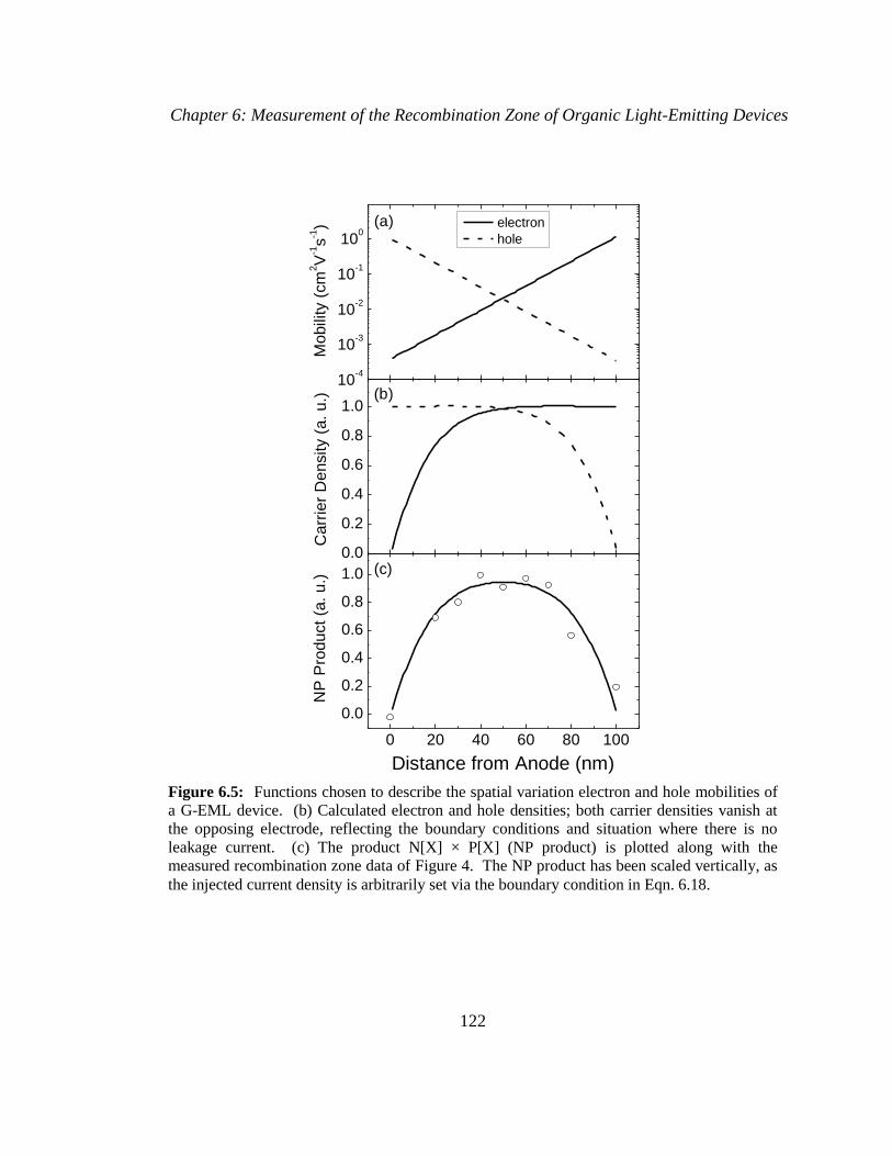
Chapter 6: Measurement of the Recombination Zone of Organic Light-Emitting Devices
122
Figure 6.5: Functions chosen to describe the spatial variation electron and hole mobilities of
a G-EML device. (b) Calculated electron and hole densities; both carrier densities vanish at
the opposing electrode, reflecting the boundary conditions and situation where there is no
leakage current. (c) The product N[X] × P[X] (NP product) is plotted along with the
measured recombination zone data of Figure 4. The NP product has been scaled vertically, as
the injected current density is arbitrarily set via the boundary condition in Eqn. 6.18.
10-4
10-3
10-2
10-1
100
Mobili
ty (
cm
2V
-1s
-1) electron
hole
0.0
0.2
0.4
0.6
0.8
1.0
Carr
ier
Density (
a.
u.)
0 20 40 60 80 100
0.0
0.2
0.4
0.6
0.8
1.0
NP
Pro
duct
(a.
u.)
Distance from Anode (nm)
(a)
(c)
(b)
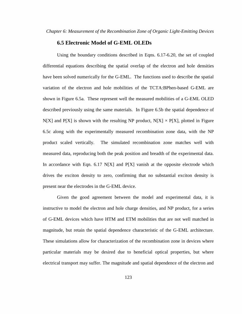
Chapter 6: Measurement of the Recombination Zone of Organic Light-Emitting Devices
123
6.5 Electronic Model of G-EML OLEDs
Using the boundary conditions described in Eqns. 6.17-6.20, the set of coupled
differential equations describing the spatial overlap of the electron and hole densities
have been solved numerically for the G-EML. The functions used to describe the spatial
variation of the electron and hole mobilities of the TCTA:BPhen-based G-EML are
shown in Figure 6.5a. These represent well the measured mobilities of a G-EML OLED
described previously using the same materials. In Figure 6.5b the spatial dependence of
N[X] and P[X] is shown with the resulting NP product, N[X] × P[X], plotted in Figure
6.5c along with the experimentally measured recombination zone data, with the NP
product scaled vertically. The simulated recombination zone matches well with
measured data, reproducing both the peak position and breadth of the experimental data.
In accordance with Eqn. 6.17 N[X] and P[X] vanish at the opposite electrode which
drives the exciton density to zero, confirming that no substantial exciton density is
present near the electrodes in the G-EML device.
Given the good agreement between the model and experimental data, it is
instructive to model the electron and hole charge densities, and NP product, for a series
of G-EML devices which have HTM and ETM mobilities that are not well matched in
magnitude, but retain the spatial dependence characteristic of the G-EML architecture.
These simulations allow for characterization of the recombination zone in devices where
particular materials may be desired due to beneficial optical properties, but where
electrical transport may suffer. The magnitude and spatial dependence of the electron and

Chapter 6: Measurement of the Recombination Zone of Organic Light-Emitting Devices
124
hole mobilities examined are shown in Figure 6.6a and 6.6b. To simplify comparisons
going forward, each case is identified by the ratio of the electron-to-hole mobility at the
midpoint of the device, μR = 0.01, 0.1, 10, 100. The resulting N[X] and P[X] are shown
in Figure 6.6c and 6d for μR = 0.01 and 0.1, and μR = 10 and 100, respectively. The NP
products for μR = 0.01 and 0.1 is shown in Figure 6.6e, with the NP products for μR = 10
and 100 shown in Figure 6.6f.
Figure 6.6: Spatial variation of electron and hole mobilities for G-EML devices where the
ratio of electron to hole mobility is: μR = 0.01and μR = 0.1. (b) Spatial variation of electron
and hole mobilities for G-EML devices where μR = 10 and μR = 100. The calculated N[X] and
P[X] for the mobilities shown in (a) and (b) are shown in (c) and (d), respectively. The
resulting NP product of the carrier densities of (c) are shown in (e), while the NP product for
the carrier densities of (d) are shown in (f).
10-4
10-2
100
102
R=0.01
R=0.1
Mo
bili
ty (
cm
2V
-1s
-1) / electron
hole
R=100
R=10
0.0
0.5
1.0
P[x]
Ch
arg
e D
ensity (
a.
u.)
N[x]N[x]
P[x]
0 20 40 60 80 100
0.0
0.2
0.4
0.6
0.8
1.0
NP
Pro
du
ct
(a.
u.)
Distance from Anode (nm)
0 20 40 60 80 100
Distance from Anode (nm)
(a) (b)
(c) (d)
(e) (f)
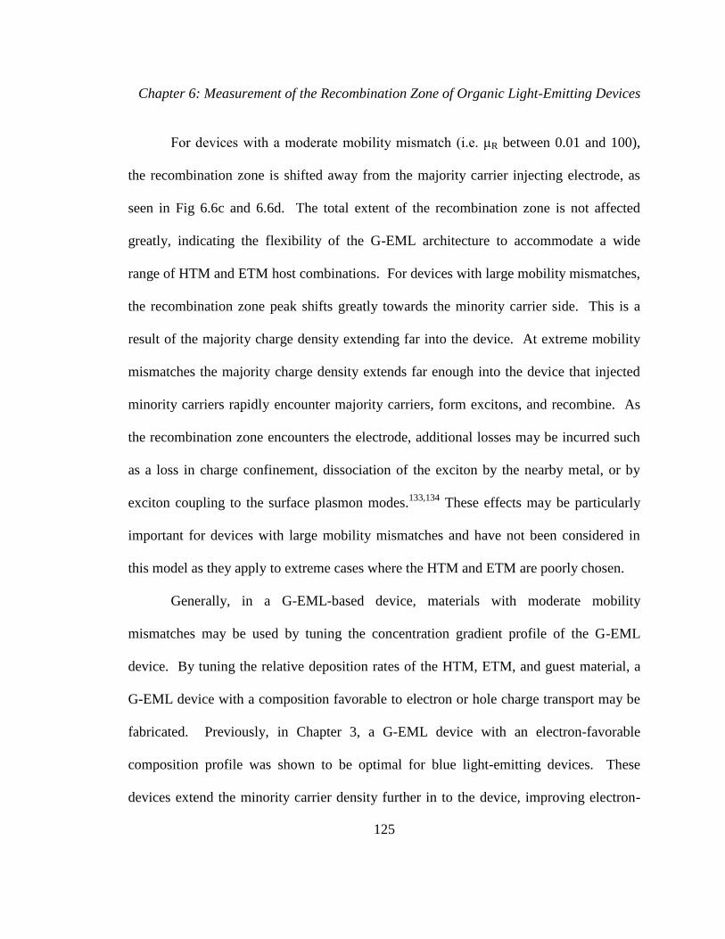
Chapter 6: Measurement of the Recombination Zone of Organic Light-Emitting Devices
125
For devices with a moderate mobility mismatch (i.e. μR between 0.01 and 100),
the recombination zone is shifted away from the majority carrier injecting electrode, as
seen in Fig 6.6c and 6.6d. The total extent of the recombination zone is not affected
greatly, indicating the flexibility of the G-EML architecture to accommodate a wide
range of HTM and ETM host combinations. For devices with large mobility mismatches,
the recombination zone peak shifts greatly towards the minority carrier side. This is a
result of the majority charge density extending far into the device. At extreme mobility
mismatches the majority charge density extends far enough into the device that injected
minority carriers rapidly encounter majority carriers, form excitons, and recombine. As
the recombination zone encounters the electrode, additional losses may be incurred such
as a loss in charge confinement, dissociation of the exciton by the nearby metal, or by
exciton coupling to the surface plasmon modes.133,134
These effects may be particularly
important for devices with large mobility mismatches and have not been considered in
this model as they apply to extreme cases where the HTM and ETM are poorly chosen.
Generally, in a G-EML-based device, materials with moderate mobility
mismatches may be used by tuning the concentration gradient profile of the G-EML
device. By tuning the relative deposition rates of the HTM, ETM, and guest material, a
G-EML device with a composition favorable to electron or hole charge transport may be
fabricated. Previously, in Chapter 3, a G-EML device with an electron-favorable
composition profile was shown to be optimal for blue light-emitting devices. These
devices extend the minority carrier density further in to the device, improving electron-

Chapter 6: Measurement of the Recombination Zone of Organic Light-Emitting Devices
126
hole overlap while maintaining charge and exciton confinement, retaining the large
recombination zone. High efficiency may then be realized in a wide range of simplified
devices where particular active materials are desirable, despite a mismatch in mobilities.
6.6 Impact of Recombination Zone on Efficiency Roll-Off
The four main parameters which govern the ηEQE roll-off of an OLED are: the
relative rate constants of TTA and TPQ, τ, and the recombination zone width. While the
first three parameters depend primarily on materials selection, the recombination zone, as
has been demonstrated here, is strongly device design-dependent. One way to
quantitatively compare the efficiency roll-off of different architectures is to note the
current density at which the ηEQE has rolled-off to half of its maximum, or “J0.”14
Therefore, the peak-normalized ηEQE of the three device structures of interest are shown
in Figure 6.7, with relevant device parameters presented in Table 6.1. Here, a reduction
in the efficiency roll-off with current density is observed in devices characterized by a
larger exciton recombination zone, as shown by an increased value for J0 in the M-EML
and G-EML structures relative to the D-EML. It is interesting to note that despite the
larger recombination zone of the G-EML device relative to the M-EML, the efficiency
roll-off in these devices is very similar. This may suggest that important parameters,
such as the polaron density and the degree of charge confinement, differ significantly in
each device. Further work is needed to fully quantify and decouple the role of the
exciton recombination zone from other contributing factors that determine the efficiency
roll-off.

Chapter 6: Measurement of the Recombination Zone of Organic Light-Emitting Devices
127
The efficiency roll-off in these devices is addressed in greater detail in Chapter 8.
6.7 Conclusions and Acknowledgments
A method to quantitatively measure the width and location of the exciton
recombination zone in an OLED has been developed and is generally independent of
emissive layer architecture. This technique demonstrates a high sensitivity to the
presence of guest excitons, a high degree of spatial resolution, and does not alter charge
transport in the OLED. We demonstrate a strong dependence of both the location and
spatial extent of the exciton recombination zone on the emissive layer architecture.
Figure 6.7: Peak-normalized ηEQE for D-EML, M-EML, and G-EML OLEDs. The J0 for
each device is: 160 mA cm-2
, 375 mA cm
-2, and 360 mA cm
-2, for D-EML, M-EML, and G-
EML, respectively.
Table 6.1: Device parameters for the architectures of interest: Peak ηEQE, measured
recombination zone (RZ) width, and roll-off parameter J0, defined as the current density where
ηEQE rolls-off to half its peak value, for the D-EML, M-EML, and G-EML device architectures
Device Architecture Peak ηEQE (%) RZ width (nm) J0 (mA cm-2
)
D-EML 11.8 15 160
M-EML 12.2 40 375
G-EML 16.9 80 360
0 100 200 300 400 5000.4
0.5
0.6
0.7
0.8
0.9
1.0
Norm
aliz
ed
EQ
E (
%)
Current Density (mA cm-2)
M-EML
G-EML
D-EML

Chapter 6: Measurement of the Recombination Zone of Organic Light-Emitting Devices
128
OLEDs based on M- and G-EML architectures have much larger recombination zones
than devices based on a D-EML architecture, with the G-EML architecture showing a
recombination zone which spans the entire device. This strong correlation emphasizes
the need to couple efforts aimed at engineering OLED architecture with direct
measurements of the exciton recombination zone. Quantitative insight into the exciton
recombination zone is essential as a tool to guide OLED design and to better inform and
evaluate critically needed models of operation.
Chapter 7: Engineering Efficiency Roll-Off in Organic Light-Emitting Devices
129
Chapter 7 - Engineering Efficiency Roll-Off in Organic Light-
Emitting Devices
As mentioned previously, one development which has enabled high peak external
quantum efficiency (ηEQE) is the ability to harvest triplet excitons for electroluminescence
(EL). The utilization of triplet excitons occurs via three pathways: (1) directly as
radiative decay, i.e. electrophosphorescence,13,57,58,60,69
or indirectly, from (2) triplet-
triplet annihilation processes which result in the formation of a singlet exciton,166–170
or
(3) singlet states which are populated through reverse intersystem crossing from triplet
states, as in thermally activated delayed fluorescence (TADF).50,171–173
All of these
routes, however, require population of the triplet exciton state through electrical
excitation. Triplet excitons typically have long natural lifetimes, on the order of 10-6
-10-
3s.
13–16 A consequence of the long lifetime is that at the high current densities often
necessary to achieve high brightness levels, large triplet exciton densities are produced.
These high densities result in exciton density-driven quenching processes, which are
observed as a decrease in the ηEQE with increasing current density (and thus increasing
brightness), a characteristic termed the “efficiency roll-off.”15,82,86,129,130,151
The
efficiency roll-off is one factor which limits the implementation of OLEDs in high
brightness applications. Further, it has been suggested that device operating lifetimes
may suffer in devices with a high degree of efficiency roll-off, as larger current densities
are needed to reach high operating brightness levels.82,174–177

Chapter 7: Engineering Efficiency Roll-Off in Organic Light-Emitting Devices
130
7.1 Density-Driven Exciton Quenching Processes
The physical processes which are responsible for exciton quenching in
phosphorescent OLEDs have been previously identified as triplet-triplet annihilation and
triplet-polaron quenching.14,15,129,130,150,152
The impact of these processes on the triplet
exciton population can be written separately as:
(7.1)
for triplet-triplet annihilation, and
(7.2)
for triplet-polaron quenching, where nex is the triplet exciton population, which may
depend on position within the emissive layer, τ is the exciton lifetime, κTT is the rate of
triplet-triplet annihilation, κTP is the rate of triplet-polaron annihilation, G is an exciton
generation term, and ρ is the polaron density, which depends on position and which may
be a function of the current density, J, or voltage, V, depending on the description of
charge transport.121,150,178
In Eqn. (7.2), the spatial overlap of polarons and excitons in
the device is of particular importance. This property, however, is difficult to probe
directly, thus the rate constant κTP reflects not only the strength of the interaction of
polarons and excitons but also the spatial overlap.15
Under device operating conditions,
the exciton population becomes:14,15
(7.3)
where the final term represents electrical generation of excitons, e is the elementary
charge, and W is the width of exciton recombination zone in the device. Written this
Chapter 7: Engineering Efficiency Roll-Off in Organic Light-Emitting Devices
131
way, the generation term assumes all injected carriers form excitons, which may be the
case for devices with a high degree of charge balance. Previously, loss of charge balance
has been identified as a contributing factor to the efficiency roll-off observed in
devices.129
Loss of charge balance may be mitigated through device design, either
through material selection or the incorporation of charge blocking layers. Whereas κTT,
κTP, and τ are typically considered material parameters and are generally independent of
device design in typical OLED architectures, the exciton recombination zone in an OLED
is dependent on the overlap of electron and hole charge densities, and thus is sensitive to
the architecture of the device, particularly the emissive layer design.
7.2 Experimental Design
7.2.1 Device Architectures of Interest
There are a variety of emissive layer architectures which have shown high peak
efficiencies, including double-emissive layer (D-EML), mixed-emissive layer (M-EML),
and graded-emissive layer (G-EML) devices.80,81,87–89,103,113,115
The D-EML consists of
two distinct layers, a hole-transport layer (HTL) and an electron transport layer (ETL),
both doped uniformly with a dilute emissive guest. This architecture can achieve high a
degree of charge balance and strongly confines the charge carriers to a region near the
HTM:ETM interface. The M-EML design consists of a uniformly mixed layer of HTM
and ETM that is doped with the emissive guest. This design allows for the charge carrier
mobilities of the composite layer to be tuned by varying the HTM:ETM ratio, ideally
achieving ambipolar characteristics to maximize charge balance and efficient exciton

Chapter 7: Engineering Efficiency Roll-Off in Organic Light-Emitting Devices
132
formation.89
The G-EML device is a single-layer device architecture which consists of a
continuously varying composition profile, from nearly 100% HTM at the anode to nearly
100% ETM at the cathode, doped throughout with an emissive guest.113
This device
architecture has been previously used to achieve high ηEQE in red-, green-, and blue-light
emitting devices.115
Whereas the G-EML device may be optimized by tuning the composition gradient
profile (as demonstrated in Chapter 3), the D-EML and M-EML device architectures
often require the use of charge and exciton blocking and transport layers to achieve high
peak performance. Optimization in these devices is done by adjusting the doping
concentration, thickness of each layer, and mixing ratio of HTM:ETM, in the M-EML
devices. These parameters are most often tuned to give low-voltage operation and high
peak-performance, though the impact these chances have on the spatial extent and
location of the recombination zone is rarely considered.
The recombination zone width of D-EML and G-EML-based devices has
previously been measured in Chapter 6, and it was found that the D-EML architecture
had a significantly reduced width (W ≈ 15 nm) compared to that of the G-EML device (W
≈ 80 nm).179
In that Chapter, it was observed that the G-EML device exhibited a
reduction in the efficiency roll-off compared to the D-EML-based device. In this Chapter
we quantitatively examine the exciton quenching processes present in both device
architectures using both transient and steady state photo- and electro-luminescence
measurements. The important quenching parameters κTT, κTP, and τ are measured

Chapter 7: Engineering Efficiency Roll-Off in Organic Light-Emitting Devices
133
independently, and the impact of the recombination zone width on efficiency roll-off is
examined directly.
7.2.2 Device Fabrication and Test Film Design
Optimized OLEDs and thin film test devices were fabricated using 4,4',4''-
tris(carbazol-9-yl)triphenylamine (TCTA) as an HTM, 4,7-diphenyl-1,10-phenanthroline
(BPhen) as an ETM, and the archetypal green phosphorescent molecule tris(2-
phenylpyridine)iridium(III) (Ir(ppy)3) as the emitter. These host materials are common to
many OLEDs and have been previously used in the fabrication of high-efficiency G-EML
OLEDs.115
To characterize the κTT and τ, thin films having a thickness of 30 nm were
fabricated on glass substrates with TCTA:Ir(ppy)3 (2 wt.%), BPhen:Ir(ppy)3 (2 wt.%), or
a uniform mixture of [TCTA:BPhen]:Ir(ppy)3 ([50:50]:2 wt.%). An optical pulse from an
N2 laser (λ=337 nm, 1 ns pulse width, 10 Hz rate) was used to generate a population of
singlet excitons on the guest which rapidly intersystem cross to the triplet state. It is
likely that under optical excitation that excitons are formed on the hosts, with host-guest
energy transfer occurring rapidly and efficiently.14
Hole-only single carrier devices were fabricated on pre-cleaned glass substrates
with ITO as a bottom contact and Au as a top contact. Films for transient
photoluminescence (PL) measurements were deposited on pre-cleaned glass substrates
with each host:guest combination of interest. Transient PL experiments were conducted
using a pulsed nitrogen laser (Optical Building Blocks) with an excitation wavelength of
λ=337 nm and a pulse length of approximately 0.5 ns. The transient PL signal was

Chapter 7: Engineering Efficiency Roll-Off in Organic Light-Emitting Devices
134
collected with a set of lenses and focused down on to a fast photodiode (Thorlabs
PDA10A). The photodiode signal was recorded using a 1GHz bandwidth oscilloscope
(Tektronix TDS5104b). The laser pulse energy was measured with a powermeter
(Coherent EnergyMax 10MB-HE). Electroluminescent transient experiments were
conducted using a pulse generator (HP 8114a) and the collection setup described above.
For the steady-state photoluminescence quenching experiments, an LED laser with a
pump wavelength λ=405 nm (B&W Tek 405-40E) was used to excite the samples, while
a large-area silicon photodiode was used to detect the emission (Hamamatsu S3584-08).
7.3 Characterizing Triplet-Triplet Annihilation
Assuming a high PL efficiency for emission,24
the luminescent output, L, is
linearly proportional to the exciton density (L[t] ~ nex[t]/τ), Eqn. 1 may be solved to
describe the transient decay of triplet excitons
[ ] [ ]
(
[ ]
)
[ ]
, (7.4)
where nex[0] is the initial population of excitons, calculated from measurements of the
initial laser intensity and the optical absorption coefficients of each sample. The
normalized transient PL decay of each material system and the fits to Eqn. 7.4 are shown
in Figure 7.1a-c for multiple initial exciton densities. In all material systems, an initial
fast decay is observed which increases with increasing excitation density. This feature is
attributed to strong exciton-exciton quenching at high exciton densities. As the exciton
population falls at longer times, due to both radiative decay and quenching events,

Chapter 7: Engineering Efficiency Roll-Off in Organic Light-Emitting Devices
135
exciton-exciton interactions decrease and the decay is dominated by the natural exciton
lifetime. The κTT and τ extracted for each system do not vary within experimental error,
and have average values of κTT = (1.9 ± 4.1) × 10-12
cm3s
-1 and τ = (1.62 ± 0.19) × 10
-6 s.
The average is used hereafter as κTT reflects the interaction of the emissive guest with
Figure 7.1: Transient photoluminescence decays for (a) TCTA:Ir(ppy)3, (b) BPhen:Ir(ppy)3
and (c) TCTA:BPhen:Ir(ppy)3 thin films at different initial exciton densities. Fits to Eqn. 7.4
for each measurement are shown as solid lines.
10-2
10-1
100 TCTA:Ir(ppy)
3
3.2 x 10¹⁹
cm-3
8.9 x 10¹⁸
cm-3
8.9 x 10¹⁷
cm-3
No
rma
lize
d P
ho
tolu
min
esce
nce
(a
. u
.)
10-2
10-1
100 BPhen:Ir(ppy)
3
1.7 x 10¹⁹
cm-3
6.1 x 10¹⁸
cm-3
1.7 x 10¹⁷
cm-3
0 1 2 3 4 5 6 7
10-2
10-1
100 TCTA:BPhen:Ir(ppy)
2.0 x 10¹⁹
cm-3
5.6 x 10¹⁸
cm-3
5.6 x 10¹⁷
cm-3
Time (s)
(a)
(b)
(c)
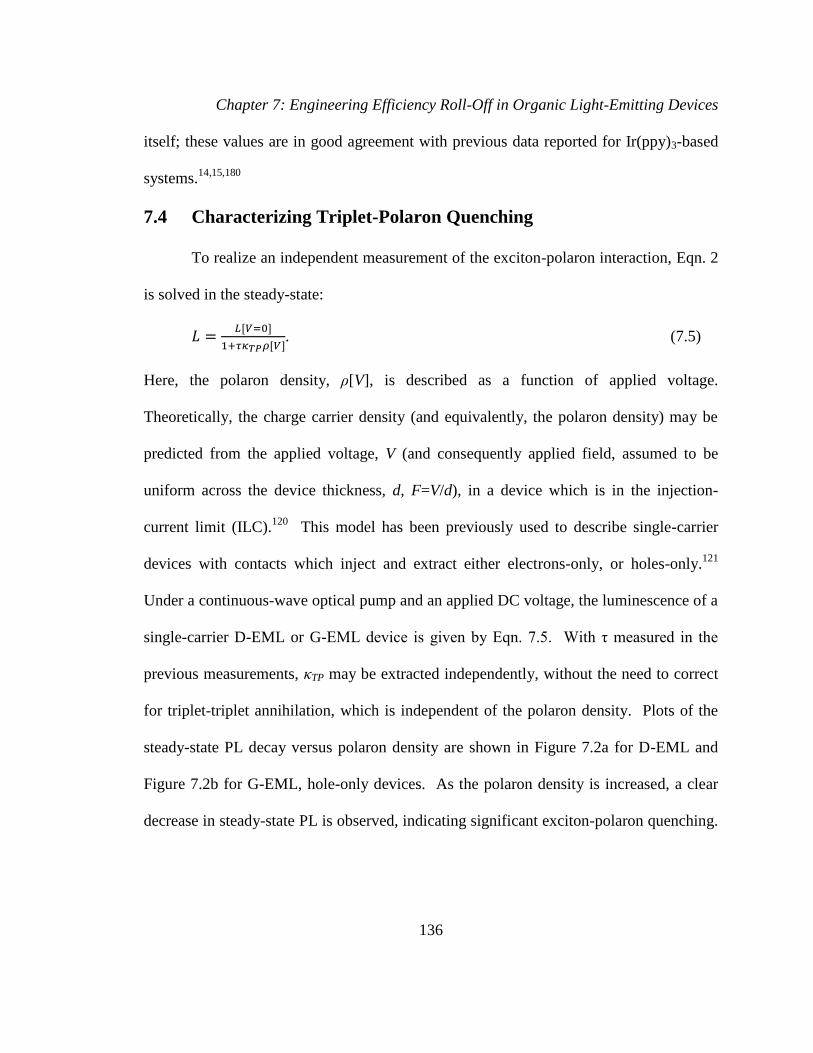
Chapter 7: Engineering Efficiency Roll-Off in Organic Light-Emitting Devices
136
itself; these values are in good agreement with previous data reported for Ir(ppy)3-based
systems.14,15,180
7.4 Characterizing Triplet-Polaron Quenching
To realize an independent measurement of the exciton-polaron interaction, Eqn. 2
is solved in the steady-state:
[ ]
[ ]. (7.5)
Here, the polaron density, ρ[V], is described as a function of applied voltage.
Theoretically, the charge carrier density (and equivalently, the polaron density) may be
predicted from the applied voltage, V (and consequently applied field, assumed to be
uniform across the device thickness, d, F=V/d), in a device which is in the injection-
current limit (ILC).120
This model has been previously used to describe single-carrier
devices with contacts which inject and extract either electrons-only, or holes-only.121
Under a continuous-wave optical pump and an applied DC voltage, the luminescence of a
single-carrier D-EML or G-EML device is given by Eqn. 7.5. With τ measured in the
previous measurements, κTP may be extracted independently, without the need to correct
for triplet-triplet annihilation, which is independent of the polaron density. Plots of the
steady-state PL decay versus polaron density are shown in Figure 7.2a for D-EML and
Figure 7.2b for G-EML, hole-only devices. As the polaron density is increased, a clear
decrease in steady-state PL is observed, indicating significant exciton-polaron quenching.

Chapter 7: Engineering Efficiency Roll-Off in Organic Light-Emitting Devices
137
Electric field-induced exciton quenching has been previously suggested as a loss
pathway, however, such effects are only observed at very high fields (F > 2.5 MV/cm),
greater than those used in the present study (F < 2.0 MV/cm). Interestingly, the values of
κTP extracted for D-EML and G-EML devices are similar, κTP = (6.3 ± 4.7) × 10-13
cm3s
-1
and κTP = (2.8 ± 1.6) × 10-13
, respectively. These values are in good agreement with
those previously reported by Reineke et al.15
for TCTA:Ir(ppy)3 devices. In that work,
the single-carrier devices were designed to be in the space-charge limited current (SCLC)
regime and the polaron density was related to the current density in a trap-filling SCLC
model.
Figure 7.2: Steady-state photoluminescence of hole-only (a) D-EML and (b) G-EML devices
at varying polaron densities. Fits to Eqn. 7.5 are shown as solid lines for each device.
0.92
0.96
1.00D-EML
G-EML
0.01 0.1 1
0.97
0.98
0.99
1.00
No
rma
lize
d P
ho
tolu
min
esce
nce
(a
. u
.)
Polaron Density (x1018
cm-3)
(a)
(b)

Chapter 7: Engineering Efficiency Roll-Off in Organic Light-Emitting Devices
138
7.5 Predicting Efficiency Roll-Off in OLEDs
7.5.1 ηEQE Predictions for D-EML and G-EML Devices
A steady-state solution to Eqn. 7.3 may be found which describes the photon
output per electron input, which is equivalent to the normalized external quantum
efficiency, ηEQE, of a device. That solution, after Reineke et al., is:15
(√
), (7.6)
with
, (7.7)
𝛥 (
⁄ ), (7.8)
and
, (7.9)
where a relationship between the current density and polaron density in a full device is
assumed, ρ = CJ1/(l+1)
, and C is a constant which describes the electronic properties of the
device.15
The current density-voltage and brightness-voltage characteristics for the D-
EML and G-EML are shown in Figure 7.3a and 7.3c, respectively. The corresponding
normalized ηEQE for the devices are shown versus current density in Figure 7.3b and 7.3d
for D-EML and G-EML devices, respectively; the peak ηEQE of the D-EML device is ηEQE
= 11.3%, while the G-MEL device reaches a peak ηEQE = 16.3%. The best-fits of Eqn.
7.6 to each device are also shown in Figure 7.3b and 7.3d (solid line); the model
parameters for each fit are shown in Table 7.1. To compare the roll-off of devices with

Chapter 7: Engineering Efficiency Roll-Off in Organic Light-Emitting Devices
139
κTT
(cm3
s-1
)
κTP
(cm3
s-1
)
τ
(s) W
(nm)
D-EML (Measured) 1.9× 10⁻¹²
6.3 × 10⁻¹³
1.62 × 10⁻⁶
15 D-EML (Best Fit) 2.1 × 10
-12
0
G-EML (Measured) 1.9× 10⁻¹²
2.8 × 10⁻¹³
80
G-EML (Best Fit) 5.7 × 10⁻¹²
2.8 × 10⁻¹³
Table 7.1: Measured rate constants for triplet-triplet annihilation (κTT), triplet-polaron
quenching (κTP), measured exciton lifetime (τ), and measured recombination zone width (W)
for D-EML and G-EML OLEDs.
Figure 7.3: (a) Current density-voltage, brightness-voltage and (b) normalized ηEQE for the D-
EML device. (c) Current density-voltage, brightness-voltage and (d) normalized ηEQE for the
G-EML device. Fits to Eqn. 6 of the ηEQE of each device are shown as solid lines. The J0 of
each device is noted, J0 = 170 mA/cm2 for the D-EML device, J0 = 325 mA/cm
2 for the G-
EML device.
10-8
10-6
10-4
10-2
100
102
10-2
100
102
104
106
100
102
104
106
Curr
ent
Density (
mA
cm
-2) D-EML
0.2
0.4
0.6
0.8
1.0
0.1 1 1010
-8
10-6
10-4
10-2
100
102
G-EML
Curr
ent
Density (
mA
cm
-2)
Voltage (V)
G-EML
J0 = 325 mA cm
-2
D-EML
J0 = 170 mA cm
-2
100
101
102
103
0.2
0.4
0.6
0.8
1.0
Norm
aliz
ed
EQ
E
Current Density (mA cm-2)
Brightn
ess (
cd m
-2)
Brightn
ess (
cd m
-2)
(a)
(c)
(b)
(d)

Chapter 7: Engineering Efficiency Roll-Off in Organic Light-Emitting Devices
140
different peak ηEQE, the current density at which the efficiency decreases to half of its
maximum, termed “J0,” is noted, J0 = 170 mA cm-2
for the D-EML and J0 = 325 mA cm-2
.
As has been observed previously, the G-EML device exhibits significantly less efficiency
roll-off than the D-EML device.
For the G-EML device, best-fits of Eqn. 7.6 were achieved by allowing κTT and
κTP to vary; the resulting values are within the experimental error bars, indicating the high
degree of accuracy with which the model (and measured values of W, κTT, κTP, and τ)
replicates the measured ηEQE. In the case of the D-EML device, the best-fit κTT constant
is similarly within experimental error, see Table 7.1. However, the best-fit value of κTP
for the D-EML devices is essentially zero, in contrast to the measured value of κTP from
the above experiments. This discrepancy likely arises from the different distributions of
excitons and polarons within the test films compared to actual device operation. In the
test films, excitons are created throughout the film, according the optical field distribution
and the absorption properties of the materials; however, in the D-EML device, excitons
are only present near the HTM:ETM interface. This likely results in a much lower
exciton-polaron density overlap in the D-EML device, which in turn reduces the best-fit
value of κTP, which, in the framework of Eqn. (7.2), reflects both the interaction and
spatial overlap of excitons and polarons.
To verify this impact, the steady-state PL of hole-only devices with an alternate
D-EML structure of: ITO (150 nm) / TCTA (45 nm) / TCTA:Ir(ppy)3 (5 wt.%, 5 nm) /
BPhen:Ir(ppy)3 (5 wt.% 5 nm) / UGH2 (45 nm) / Au (50 nm), was examined where

Chapter 7: Engineering Efficiency Roll-Off in Organic Light-Emitting Devices
141
UGH2 is the wide-gap molecule: 1,4-bis(triphenylsilyl)benzene.69
In this configuration,
excitons are only generated on the Ir(ppy)3 molecules, which is present in a narrow
region of the device, such as in the narrow-recombination zone D-EML OLEDs. In that
test device, no decrease in steady-state PL was observed with polaron densities up to 1019
cm-3
(see Figure 7.4), giving κTP ≈ 0, in agreement with the fits of device ηEQE. Clearly,
both triplet-triplet annihilation and triplet-polaron quenching are processes which affect
the roll-off of G-EML devices, while the roll-off of D-EML is dominated by triplet-triplet
annihilation. In both cases, the recombination zone width is fixed to experimentally-
measured values, and, given the good agreement of the ηEQE data and fits to Eqn. 7.6, is a
key parameter in determining the efficiency roll-off.
Figure 7.4: Triplet polaron quenching for a D-EML device with a narrow spatial overlap of
charges and excitons. Data from three devices show no observable decrease in steady-state
luminescence with increasing injected polaron density.
0.01 0.1 1 100.9950
0.9975
1.0000
1.0025
1.0050
No
rma
lize
d In
tensity (
a.
u.)
Polaron Density (x 1018
cm-3)
Device 1
Device 2
Device 3

Chapter 7: Engineering Efficiency Roll-Off in Organic Light-Emitting Devices
142
7.5.2 Transient Electroluminescence of D-EML and G-EML Devices
The cumulative effects of triplet-triplet annihilation and triplet-polaron quenching
can be seen under device operating conditions in transient EL. These quenching
processes are observed as a reduction in the total exciton lifetime, particularly under high
excitation. Transient EL may therefore be used to show the impact of recombination
zone width on the quenching processes in an OLED. Voltage pulses with a width of 250
ns and period of 200 μs were applied to D-EML and G-EML devices with varying peak
voltage, V, the resulting transient EL decays are shown in Figure 7.5a for V = 25 V. In
transient EL, the effects of triplet-triplet annihilation and triplet-polaron quenching can be
seen as reduction in the effective exciton lifetime. Previously, transient EL decays have
been fit using bi-exponential equations with short and long lifetimes, τ1 and τ2,
respectively.14
The short lifetime has been previously associated with host-guest
interactions, while the long lifetime has been associated with guest exciton decay.14
The
fitted values of τ1 and τ2 are shown in Figure 7.5b for a range of voltages for both D-EML
and G-EML devices. At low peak voltage pulses, both devices approach a common value
of τ2 which is close agreement with the lifetime value measured in the PL transient
experiments. At high peak voltage pulse, the value of τ2 decreases drastically in the D-
EML devices, relative to the G-EML device. The longer-lived EL transients of the G-
EML devices, compared to the D-EML devices, indicate the role the wide recombination
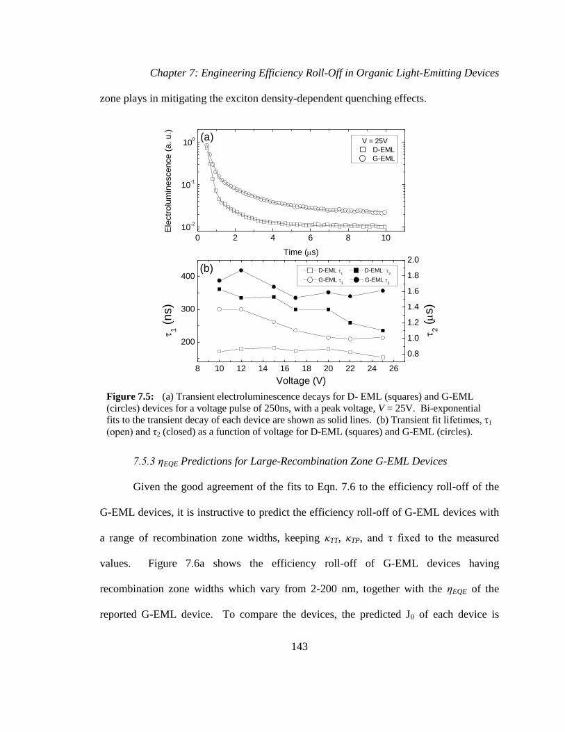
Chapter 7: Engineering Efficiency Roll-Off in Organic Light-Emitting Devices
143
zone plays in mitigating the exciton density-dependent quenching effects.
7.5.3 ηEQE Predictions for Large-Recombination Zone G-EML Devices
Given the good agreement of the fits to Eqn. 7.6 to the efficiency roll-off of the
G-EML devices, it is instructive to predict the efficiency roll-off of G-EML devices with
a range of recombination zone widths, keeping κTT, κTP, and τ fixed to the measured
values. Figure 7.6a shows the efficiency roll-off of G-EML devices having
recombination zone widths which vary from 2-200 nm, together with the ηEQE of the
reported G-EML device. To compare the devices, the predicted J0 of each device is
Figure 7.5: (a) Transient electroluminescence decays for D- EML (squares) and G-EML
(circles) devices for a voltage pulse of 250ns, with a peak voltage, V = 25V. Bi-exponential
fits to the transient decay of each device are shown as solid lines. (b) Transient fit lifetimes, τ1
(open) and τ2 (closed) as a function of voltage for D-EML (squares) and G-EML (circles).
0 2 4 6 8 10
10-2
10-1
100
0.8
1.0
1.2
1.4
1.6
1.8
2.0
Ele
ctr
olu
min
escence (
a. u.)
Time (s)
V = 25V
D-EML
G-EML
8 10 12 14 16 18 20 22 24 26
200
300
400
1 (
ns)
Voltage (V)
D-EML 1 D-EML
2
G-EML 1 G-EML
2
2 (s)
(a)
(b)

Chapter 7: Engineering Efficiency Roll-Off in Organic Light-Emitting Devices
144
plotted versus recombination zone width in Figure 7.6b. As seen in Figure 7.6b, there is
a sharp increase in J0 for a moderate increase in W, particularly at low recombination
zone widths. For devices with inherently small recombination zones, engineering a small
improvement in recombination zone width may have a large impact on the efficiency
roll-off. In all devices, engineering the recombination zone width offers a route towards
improving the efficiency roll-off in OLEDs.
Figure 7.5: (a) Normalized ηEQEs for G-EML devices with varying recombination zone
widths, as predicted from Eqn. 6. Measured data for the G-EML device used in the present
study is shown (circles) together with the best fit to Eqn. 6. (bold line). (b) The J0 of each
predicted device is shown versus recombination zone width.
Increasing RZ Width
10-2
10-1
100
101
102
103
0.0
0.2
0.4
0.6
0.8
1.0
Norm
aliz
ed
EQ
E (%
)
Current Density (mA cm-2)
0 50 100 150 200
101
102
103
J0 (
mA
cm
-2)
Recombination Zone Width (nm)
(a)
(b)

Chapter 7: Engineering Efficiency Roll-Off in Organic Light-Emitting Devices
145
7.6 Conclusions
In summary, the four main parameters which impact efficiency roll-off in OLEDs
(κTT, κTP, τ, and W) have been measured independently for D-EML and G-EML devices.
A model of the efficiency roll-off which is based on those parameters was used to
accurately predict the performance of the OLEDs of interest. In the case of the G-EML
device, it was found that the ηEQE was well-predicted by measured values of κTT and κTP,
with the recombination zone fixed according to previous experimental results. In the D-
EML device, the ηEQE was best-predicted using only κTT, with κTP ~ 0. These results
indicate that triplet-triplet annihilation and triplet-polaron quenching are processes which
impact the efficiency roll-off of G-EML devices, while the D-EML device efficiency
roll-off is dominated by triplet-triplet annihilation. Further, the G-EML device exhibited
significantly less efficiency roll-off, due in large part to the wide recombination zone
present in that device. Using the model of efficiency roll-off, predictions of the efficiency
roll-off of G-EML devices with varying recombination zones were shown to have
drastically different degrees of efficiency roll-off, further evidence of the large role the
exciton recombination zone plays in efficiency roll-off. In the future, the G-EML device
architecture may offer a route towards engineering efficient, single-layer OLEDs which
have large recombination zones, thus reducing the efficiency roll-off and extending the
range of useful brightness levels in OLED applications.

Chapter 8: Optical Modeling of OLEDs
146
Chapter 8 - Optical Modeling of OLEDs
Previous models in this thesis have been aimed at understanding and predicting
the electronic properties of OLEDs. Equally important to consider is the optical design
of the OLEDs, i.e. the spatial distribution of the optical electric field within the device.
The optical field within a structure impacts the angular distribution and efficiency of far-
field light extraction and, in some cases, may alter the lifetime of the exciton.181–185
The
efficiency with which photons generated in the device escape in the forward viewing
direction, or outcoupling efficiency (ηOC) has been briefly introduced in Chapter 2. In
that chapter a rough estimate of ηOC = 20% was made, in accordance with typical values
reported in the literature. However, the exact value and wavelength dependence of ηOC is
more complicated, and may vary greatly depending on the layer structure of the device.
A more accurate prediction of ηOC requires knowledge of the optical density of states
which couple to the far-field at each emitter molecule location.186
This is done by
calculating the optical electric field throughout the multilayer structure of an OLED. A
predictive model of the optical field requires knowledge of the complex index of
refraction and thickness of each material. These properties are independently
measureable; in this work they are measured by spectroscopic ellipsometery.

Chapter 8: Optical Modeling of OLEDs
147
8.1 Theory of Optical Fields in OLEDs
8.1.1 Transfer-Matrix Model of Optical Electric Fields
In this optical model,182
the OLED is represented by a series of 2 × 2 matrices
which describe the transmission, reflection, and absorption of light at each interface and
within each layer. Each layer in the OLED is assumed to be homogeneous and isotropic,
with respect to its complex index of refraction, and each interface is assumed to be planar
and parallel to the other layers of the device. Light propagation in the structure is
assumed to be normal to the plane of the device (designate as the z-axis), with off-axis
components specified at angles relative to the normal axis (θj), this scheme is depicted in
Figure 8.1. The propagation of the optical electric field through layer j is given by:
[
]. (8.1)
Figure 8.1: General representation of a multilayer optical structure having m layers. Each
layer has a thickness of dj and an angle of refraction, θj. The electric field in each layer is
represented by two components propagating in positive and negative direction (normal to
layer, E+
j and E-j, respectively). The impact on the electric field due to propagation across
interfaces is described by the matrix Ij,k and propagation through layers is described by the
matrix Lj.
θ0
Ambient Layer 1 Layer j Layer m
[E1
+
E1 ]
Ej+
E𝑗 [
E0+
E0 ] [
Em+
E𝑚 ]
dj
I0,1 L1 Ij-1,j Lj Im-1,m Lm
θ1 θj θmz

Chapter 8: Optical Modeling of OLEDs
148
And the propagation of the electric field across an interface between layers j and k is
given by:
[
]. (8.2)
Where rjk and tjk are the complex Fresnel reflection and transmission coefficients:
(8.3)
and
, (8.4)
for s-polarized (TE) light, and:
(8.5)
and
(8.6)
for p-polarized (TM) light. Here, dj is the layer thickness,
, (8.7)
and
[ ], (8.8)
where θj is the angle of refraction in layer j and nj is the complex index of refraction (nj =
ηj + iκ, where ηj is the index of refraction and κ is the extinction coefficient). The optical
electric field propagating in to (E+
0) and out of (E-0) the stack is then described by a total

Chapter 8: Optical Modeling of OLEDs
149
system transfer matrix, S, and the optical electric fields propagating at the furthest
interface (E+
m and E-m, respectively) are:
[
] [
]. (8.9)
The complete computer code for the model may be found in Appendix D. As an
example, the optical electric field of a typical D-EML device (glass with ITO (150 nm) /
TCTA:Ir(ppy)3 (40 nm) / BPhen:Ir(ppy)3 (40 nm) / Al (100 nm)) is shown in Figure 8.2a
for a single wavelength (λ = 520nm) and a contour plot of the field versus wavelength
and device thickness is shown in Figure 8.2b.
8.1.2 Dipole emission within OLEDs
To simulate the far-field light extraction efficiency of photons generated at
Figure 8.2: (a) Optical electric field of a D-EML device at λ = 520nm. The field peaks in the
TCTA:Ir(ppy)3 layer and decays rapidly in the BPhen:Ir(ppy)3 layer. (b) The full optical
electric field for the visible wavelengths at each thickness in the device. Dark colors represent
low intensity optical fields. The ITO thickness spans the 0-150 nm, the TCTA:Ir(ppy)3 spans
150-190 nm, BPhen:Ir(ppy)3 spans 190-230 nm, and the Al cathode spans the 230-330nm
thicknesses.
0 50 100 150 200 250 3000.0
0.2
0.4
0.6
0.8
1.0
No
rma
lize
d F
ield
Inte
nsity (
a.
u.)
Thickness (nm)
1.0
TCTA:
Ir(ppy)3
BPhen:
Ir(ppy)3 Al
0 50 100 150 200 250 300
400
500
600
700
800
Wavele
ngth
(nm
)
Thickness (nm)
ITO 0.010.5
(a) (b)

Chapter 8: Optical Modeling of OLEDs
150
various positions within an OLED, emission source terms must be include in the above
optical model. Emitting molecules act as local additions to the electric field:183,187
[
] [
] [
], (8.10)
where Ea and Eb are the electric fields (propagating in the positive and negative z-axis
direction) on either side of the emitting dipole, represented here as an infinitesimally
small plane at the interface between two layers in the OLED stack. Benisty et al.183
has
previously described the emission pattern of an organic molecule as randomly oriented
vertical and horizontal electric dipoles with normalized power per unit solid angle (P)
given by:
[ ], (8.11)
, (8.12)
and:
[ ], (8.13)
where the subscripts v and h refer to the orientation of the dipole (vertical or horizontal)
and the super scripts p and s refer to the polarization of the light emission (TM and TE,
respectively). The A terms of equation 8.10 are given by A +,-
= √ for each dipole and
polarization.
Chapter 8: Optical Modeling of OLEDs
151
8.2 Optical Modeling Results for D-, M-, and G-EML OLEDs
8.2.1 Optical Electric Field Results
To illustrate the power of the optical modeling technique, the optical electric
fields of the Ir(ppy)3-based D-, M-, and G-EML OLEDs are shown in Figures 8.3a-c,
respectively. Most important in these figures is the peak height and location of the
optical electric field within the emissive layers. As will be seen below, this peak shape
and height directly relate the optical density of states which couple to the far-field, i.e. the
outcoupling efficiency at each point within the emissive layers.
8.2.2 Predictions of Outcoupling Efficiency
With the models of Section 8.1 the outcoupling efficiency of the D-EML device
shown in Figure 8.3a was simulated. Given the narrow recombination zone measured in
Chapter 6, a single dipole emission plane was used at the interface between the
TCTA:Ir(ppy)3 and BPhen:Ir(ppy)3 layers; an ηOC = 18.3% was calculated. This
represents the upper limit to ηEQE in this device. The use of Ir(ppy)3 allows χ ~ 1.0 and
ηPL ≈ 100%.24
Thus, with a peak observed ηEQE = 11.7%, this gives a charge balance
factor of γ = 64%. For the M-EML and G-EML systems, the recombination zone is
significantly wider, requiring multiple dipole emission plane locations. With the above
model, this is achieved by independently calculating the outcoupling efficiency at many
points within the emissive layer. This assumes that the inclusion of the dipole emission
does not fundamentally alter the optical density of states which couple to the far-field.
For the M-EML device, the simulated ηOC versus position within the emissive layer is

Chapter 8: Optical Modeling of OLEDs
152
shown in Figure 8.4. The simulated outcoupling efficiency generally follows the shape
Figure 8.3: (a) optical electric field distributions for the D-EML OLED which has the
structure: ITO (150 nm) / TCTA:Ir(ppy)3 (5 wt. %, 40 nm) / BPhen:Ir(ppy)3 (5 wt.%, 40 nm) /
LiF (1 nm) / Al (100 nm). (b) The optical electric field for M-EML OLEDs with the structure:
ITO (150 nm) / TCTA (20 nm) / TCTA:BPhen:Ir(ppy)3 [50:50] (5 wt.%, 60 nm) / BPhen (20
nm) / LiF (1 nm) / Al (100 nm). (c) The optical electric field for G-EML OLEDs with the
structure: ITO (150 nm) / TCTA:BPhen:Ir(ppy)3 1:1 gradient (2 wt.%, 100 nm) / LiF (1 nm) /
Al (100 nm). All fields are shown for a wavelength λ = 520 nm.
0 50 100 150 200 250 300 350
No
rma
lize
d O
ptica
l F
ield
In
ten
sity (
a. u
.)
Distance from Glass/ITO interface (nm)
(a)
(b)
(c)
ITO
ITO
ITO
TCTA:Ir(ppy)3
Bphen:Ir(ppy)3
Al
Al
Al
M-EML
G-EML
T
C
T
A
B
P
h
e
n

Chapter 8: Optical Modeling of OLEDs
153
of the optical electric field in Figure 8.3b.
The simulated ηOC of the G-EML device architecture of Figure 8.3c is shown in
Figure 8.5. Again, the ηOC follows the shape of the optical field, with a maximum ~30
nm from the ITO anode and a minimum at points nearest the LiF/Al cathode. The
simulated ηOC can be weighted by the known location of excitons within the G-EML
device, i.e. the recombination zone data from Chapter 6. The recombination zone-
corrected ηOC of the entire G-EML structure is 18.9%.
Figure 8.4: Simulated ηOC for an M-EML device with the structure: glass / ITO (150 nm) /
TCTA (20 nm) / TCTA:BPhen:Ir(ppy)3 [50:50] : 5 wt.% (60 nm) / BPhen (20nm) / Al (100
nm). The simulated ηOC closely follows the optical field simulated in Figure 8.3b.
-20 -10 0 10 20 30 40 50 60 70 800
5
10
15
20
25
30
O
C (
%)
Distance from HTL (nm)
T
C
T
A
B
P
h
e
nTCTA:BPhen:Ir(ppy)3
[50:50] : 5 wt.%

Chapter 8: Optical Modeling of OLEDs
154
8.3 Summary
The realization of high-efficiency OLED operation requires the simultaneous
optimization of charge-to-exciton conversion, radiative exciton decay, and the
outcoupling of generated photons. As the results of Section 8.2 show, the ηOC of a device
is strongly dependent on device design, as the optical field shape and peak determines the
efficiency of far-field light extraction. Often, the optimization of an OLED includes
adjusting transport or emissive layer thicknesses, with the intention of reducing drive
voltage or improving charge balance in a device. However, even small changes in the
position of the emissive layer will impact the outcoupling efficiency and subsequently the
observed ηEQE. Thus the convolution of changing optical and electronic properties masks
the contribution of each in the observed performance. With the model presented in this
Figure 8.5: Simulated outcoupling efficiency (ηOC) for the G-EML device architecture. A
peak ηOC = 23.0% is predicted at a distance of 30 nm from the anode. An average ηOC =
17.2% is predicted.
0 20 40 60 80 1000
5
10
15
20
25
O
C (
%)
Distance from Anode (nm)
A
n
o
d
e
C
a
t
h
o
d
e

Chapter 8: Optical Modeling of OLEDs
155
chapter, the impact of device design on the optical performance of an OLED may be
predicted, allowing for a more complete understanding of effects of device design on
OLED operation.

Chapter 9: Single-Dopant, Single-Layer White Light-Emitting
156
Chapter 9 - Single-Dopant, Single-Layer White Light-Emitting
OLEDs
Many of the properties which make OLEDs attractive for use in displays, i.e. wide
and tunable color gamut, high efficiency, compatibility with flexible substrates, etc., are
similarly attractive for solid-state white lighting (SSL) applications. There are some
important differences, however, when considering the development of OLEDs for SSL.
The high production volume applications of lighting, industrial and home lighting, first
and foremost require cost and efficiency competiveness with available technology. Also
important is the “quality” of the light source, how well it recreates the color spectrum of a
blackbody source, often considered an ideal human light source. OLEDs certainly offer
potentially high efficiencies, evidenced by the efficiencies of single-color devices
reported in previous chapters. The issue of the quality of a light source must be an
ongoing design parameter, while the cost of a light source must be addressed at the
manufacturing level. Low-cost manufacturing may be enabled, however, if a device
architecture which meets both efficiency and quality metrics, is ‘simple,’ i.e. has low
numbers of constituent materials and few processing steps. The following chapter
presents work towards simple, efficient, and high quality white-emitting OLEDs.
9.1 Simultaneous Monomer and Excimer Emission
Recently, an interesting class of cyclometalated organic compounds have been
demonstrated which show high efficiency emission from both a monomer (i.e. triplet) and
excimer state.77,188
Excimer emission in these molecules comes from an excited state
Chapter 9: Single-Dopant, Single-Layer White Light-Emitting
157
wave function which overlaps two of the guest molecules (the term excimer is short for
“excited dimer” implying two identical species, rather than an excited complex of two
dissimilar species, termed an exciplex).189
The excimer state emission is generally broad
and red-shifted with respect to the monomer. When the molecule is designed to give blue
monomer phosphorescence, the simultaneous emission of phosphorescence and red-
shifted excimer gives a broadband emission spectrum which may be suitable for white
light applications.78,190,191
Devices fabricated with these emitters are often referred to as
“excimer whites.” Excimer white OLEDs have been previously shown to achieve high
efficiency with a variety of molecules in multilayer device architectures. In these
devices, the concentration of the emissive guest has been shown to strongly impact the
balance of monomer (blue) and excimer (red) emission. At the higher concentrations
necessary to achieve balanced white light emission, charge confinement to the guest
molecule is difficult, requiring the inclusion of special electron-blocking layers (EBLs) to
achieve high performance.192
9.2 Pt-17 in Single-Layer G-EML Devices
To address the challenges facing organic SSL, a molecule known to emit
simultaneously from monomer and excimer states was obtained from the research group
of Prof. Jian Li at Arizona State University. This molecule, platinum(II) bis(N-methyl-
imidazolyl)-toluene chloride (Pt–17),191
has shown some promise in multi-layer OLEDs,
achieving peak ηEQE = 15.7% and ηP = 27.3 lm/W with a CRI = 80. To assess the use of
Pt-17 in consort with the single-layer G-EML architecture, a series of devices with
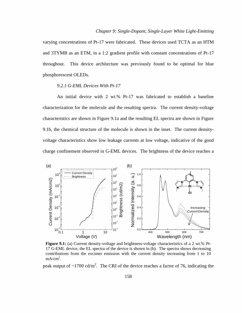
Chapter 9: Single-Dopant, Single-Layer White Light-Emitting
158
varying concentrations of Pt-17 were fabricated. These devices used TCTA as an HTM
and 3TYMB as an ETM, in a 1:2 gradient profile with constant concentrations of Pt-17
throughout. This device architecture was previously found to be optimal for blue
phosphorescent OLEDs.
9.2.1 G-EML Devices With Pt-17
An initial device with 2 wt.% Pt-17 was fabricated to establish a baseline
characterization for the molecule and the resulting spectra. The current density-voltage
characteristics are shown in Figure 9.1a and the resulting EL spectra are shown in Figure
9.1b, the chemical structure of the molecule is shown in the inset. The current density-
voltage characteristics show low leakage currents at low voltage, indicative of the good
charge confinement observed in G-EML devices. The brightness of the device reaches a
peak output of ~1700 cd/m2. The CRI of the device reaches a factor of 76, indicating the
Figure 9.1: (a) Current density-voltage and brightness-voltage characteristics of a 2 wt.% Pt-
17 G-EML device, the EL spectra of the device is shown in (b). The spectra shows decreasing
contributions from the excimer emission with the current density increasing from 1 to 10
mA/cm2.
0.1 1 1010
-7
10-5
10-3
10-1
101
103
10-3
10-2
10-1
100
101
102
103
104
105
106
Cu
rre
nt
De
nsity (
mA
/cm
2)
Voltage (V)
Current Density
Brightness
Brig
htn
ess (
cd/m
2)
400 500 600 7000.0
0.2
0.4
0.6
0.8
1.0
No
rma
lize
d I
nte
nsity (
a.
u.)
Wavelength (nm)
(a) (b)
IncreasingCurrent Density

Chapter 9: Single-Dopant, Single-Layer White Light-Emitting
159
feasibility of Pt-17 to operate as a single-dopant in a high quality SSL source. The EL of
the device shows a decreasing contribution of the excimer emission with increasing
current density. This may be due to a range of factors, including a shift in the
recombination zone as a function of current density or an electric field or charge density
effect on the population of the lower-energy excimer state. More work is required to
establish and minimize the cause of the shift, as the change may result in a noticeable
change in the color quality of the white light source. The ηEQE and ηP of the device is
shown in Figure 9.2 as a function of current density. Peak values of ηEQE = 4.6% and ηP
= 7.9 lm/W are recorded at brightness levels of ~110 and 50 cd/m2, respectively.
Figure 9.2: ηEQE and ηP of the 2 wt.% Pt-17 G-EML OLED as a function of current density.
10-3
10-2
10-1
100
101
102
0
1
2
3
4
5
0
2
4
6
8 EQE
P
E
QE (
%)
Current Density (mA/cm2)
P (
lm/W
)

Chapter 9: Single-Dopant, Single-Layer White Light-Emitting
160
9.2.2 G-EML Devices With 10 wt.% Pt-17
A second G-EML device was fabricated with 10 wt.% Pt-17 doped throughout.
The current density-voltage and brightness-voltage characteristics are shown in Figure
9.3a with the EL spectra shown in Figure 9.3b. Again, the current-density voltage
characteristics show low leakage currents. The brightness reaches much higher peak
values than in the 2 wt.% case, reaching 13,000 cd/m2 at 10 V. The EL of the device
again shows a decrease in excimer emission with increasing current density, but the
overall balance of monomer and excimer emission is more equal. The broadband spectra
of the 10 wt.% device achieves a CRI of 82 and CCT of ~4100 K, metrics better than
many current multi-layer, multi-dopant OLEDs. The ηEQE and ηP of the device is shown
in Figure 9.4 as a function of current density with peak values of ηEQE = 7.1% and ηP =
Figure 9.3: (a) Current density-voltage and brightness-voltage characteristics of a 10 wt.% Pt-
17 G-EML device, the EL spectra of the device is shown in (b). The spectra shows decreasing
contributions from the excimer emission with the current density increasing from 1 to 10
mA/cm2.
350 400 450 500 550 600 650 700 750 8000.0
0.2
0.4
0.6
0.8
1.0
1.2
Norm
aliz
ed I
nte
nsity (
a.
u.)
Wavelength (nm)0.1 1 10
10-8
10-6
10-4
10-2
100
102
104
10-3
10-2
10-1
100
101
102
103
104
105
106
Cu
rre
nt D
en
sity (
mA
/cm
2)
Voltage (V)
Current Density
Brightness
Brig
htn
ess (
cd/m
2)
(a) (b)
IncreasingCurrent Density

Chapter 9: Single-Dopant, Single-Layer White Light-Emitting
161
15.4 lm/W. These values represent a 54% enhancement in ηEQE and a nearly 95%
enhancement in ηP.
9.2.3 Summary of Pt-17 Performance in G-EML Devices
Together with the spectral shift in the EL of devices with 2 and 10 wt.% Pt-17, the
performance data indicates the large role doping concentration plays in the operation of
the excimer white devices. A range of devices with varying doping concentrations were
fabricated, and a summary of the lighting-relevant spectral data is presented in Figure 9.5.
Clearly, increased concentrations of Pt-17 push the CCT to lower values, indicating a
spectrum with increasing red emission. Higher doping concentrations result in higher
densities of the Pt-17 molecules and greater probabilities of excimer formation, which
results in relatively higher ratios of excimer to monomer emission. As the spectrum of
the device trends from monomer (blue) to excimer (red) emission, a greater percentage of
the visible spectrum, relative to a blackbody at the same temperature, is represented.
Figure 9.4: ηEQE and ηP of the 2 wt.% Pt-17 G-EML OLED as a function of current density.
10-4
10-3
10-2
10-1
100
101
102
103
0
2
4
6
8
10
0
4
8
12
16
EQE
P
E
QE (
%)
Current Density (mA/cm2)
P (
lm/W
)

Chapter 9: Single-Dopant, Single-Layer White Light-Emitting
162
This is observed as an increase in the CRI of the devices, with increasing doping
concentration, until a critical point is reached where excimer emission dominates the
monomer, finally lowering the CRI. This transition occurs around 10 wt.%, but it is
unclear how sharply this transition occurs without more concentration data points around
10 wt.%.
The peak ηEQE and ηP of the devices is shown in Figure 9.6 versus doping
concentration. The ηEQE and ηP trend to higher performance with increasing doping
concentration, peaking near 10 wt.%, though there is a broad range of doping
concentrations which give high performance. Coupled with the ability to tune CRI and
CCT of the spectrum, the broad range of doping concentrations which give good
performance makes the Pt-17-based G-EML devices attractive for further study.
Figure 9.5: Color render index (CRI) and color coordinated temperature (CCT) versus Pt-17
concentration (wt. %) in 1:2 TCTA:3TPYMB G-EML devices.
0 2 4 6 8 10 12 14 16
76
78
80
82
84
3000
4000
5000
6000
7000
8000
CR
I
PT-17 Doping Concentration (wt. %)
CRI
CCT
CC
T (
K)

Chapter 9: Single-Dopant, Single-Layer White Light-Emitting
163
9.3 Conclusions and Future Work
The above study has yielded promising results in the pursuit of simply-fabricated,
high performing, and quality solid-state light white light sources. The ability to tune the
doping concentration of an excimer white dopant to simultaneously maximize the quality
and efficiency of a device renders the single-dopant, single-layer devices presented here
attractive for use in SSL applications. Given the high ηEQE of multi-layer devices with
similar molecules,191
it is conceivable that further optimization of the G-EML devices
could yield ηP>30 lm/W, a significant milestone in the pursuit of simple white OLEDs.
Further optimization of the G-EML structure should focus on the impact of doping
Figure 9.6: Peak ηEQE and ηP for varying PT-17 doping concentrations (wt. %). Best
performance is observed in the 10 wt.% device, with a corresponding CRI = 82 and CCT =
4000 K.
0 2 4 6 8 10 12 14 160
2
4
6
8
10
0
2
4
6
8
10
12
14
16
E
QE (
%)
PT-17 Doping concentration (wt. %)
EQE
P
P(lm
/W)

Chapter 9: Single-Dopant, Single-Layer White Light-Emitting
164
concentration on the electrical properties of the G-EML device. At concentrations of 10
wt.% or greater, the dopant may significantly participate in charge transport, by trapping
or by conducting charge through dopant energy levels. Further, a greater range of host
materials should be explored to maximize the charge density overlap in the device,
improving exciton (and excimer) formation, and further increasing the efficiency.

Chapter 10: Future Research Directions
165
Chapter 10 - Future Research Directions
10.1 Summary of This Thesis
This thesis has sought understanding of the device design and materials selection
rules which result in particular OLED properties: high peak efficiency, simple
fabrication, tunable charger carrier and exciton densities, low efficiency roll-off, color,
and others. There are several areas of OLED research which can build from these device
and model results. In the following sections, potential research topics are presented
which extend concepts from the previous chapters. The goals of these research topics
reflect the state of the field; some are related to device engineering for efficiency and
operating lifetime, while others seek to drastically shift the current understanding of the
interplay between device design, device performance, and materials properties.
While organic light-emitting devices are currently being commercialized in the
form of small, mobile displays, other promised applications, such as large-area displays,
fully flexible displays, and solid-state white lighting, are not yet commercially
viable.193,194
There are several areas of OLED research with significant scientific merit
which deserve academic investigations. Chapter 9 presented work on simplified white
light-emitting devices. As stated in that chapter, the lighting market is particularly
sensitive to cost, efficiency, and quality of the light source. Additional work on
achieving highly-efficient, quality lighting in a simple device design is one important
area of future research. Related to the issue of cost in white lighting applications (and in
all OLED applications), is the longevity of device operation. Current devices exhibit

Chapter 10: Future Research Directions
166
marked efficiency decrease over time, requiring higher voltages to achieve consistent
brightness output. The physical process which lead to the decrease in the observed
efficiency are not well understood, nor are the degradation mechanisms or chemical
reactions well detailed. Chapter 7 showed promising work on reducing the efficiency
roll-off of OLEDs, however, there are several possible routes towards improving the roll-
off. Finally, the realization of an electrically-pumped organic laser has eluded this field,
one intermediate step is presented as a thought experiment.
10.2 White OLEDs
10.2.1 Simple, High-Quality White OLEDs
The white light-emitting OLEDs presented in Chapter 9 utilized a single dopant to
achieve broad-band emission. This design is attractive for its simplicity, and promising
results were shown. However, the range of molecules which have shown simultaneous
phosphorescent monomer and excimer emission is narrow, potentially limiting the
performance and quality of single-doped white OLEDs. One device design which
expands the library of possible dopants while maintaining processing simplicity is the use
of a multi-dopant, single-layer gradient.
The results of Chapter 6 clearly indicate the presence of a large exciton
recombination zone in G-EML devices. It is possible, then, that doping strips of the G-
EML device separately with red-, green-, and blue-emitting molecules would give
broadband emission, as the each molecule would ‘sample’ the exciton recombination
zone. A schematic of this concept is shown in Figure 10.1 for a 1:2 G-EML device.

Chapter 10: Future Research Directions
167
There are many ways in which a device like this might be tuned for both high efficiency
and high quality. The thickness of each dopant region, doping concentration, and the
order of the dopants might be adjusted (red-green-blue (RGB) or blue-green-red (BGR),
etc.) to tune color and efficiency. The gradient profile might be adjusted such that the
recombination zone, predicted from Chapter 6, has a larger or smaller overlap with a
particular doped region. First and foremost, however, the optical field of any structure of
interest must be known. As was shown in Chapter 8, the outcoupling efficiency of a G-
EML OLED may vary greatly with respect to the position of the emitting molecule within
the device, this effect must be considered when analyzing any multi-dopant, single-layer
white OLED.
Figure 10.1: Schematic of a multi-dopant, single-layer OLED with a 1:2 HTM:ETM gradient
profile. The position of the dopant, doping concentration, thickness of the doped regions, and
gradient profile might all be adjusted to give peak white light-emission performance.
0 20 40 60 80 1000
20
40
60
80
100
HTM
ETMCom
positio
n (
wt. %
)
Device Thickness (nm)
Dopant 1 Dopant 2 Dopant 3

Chapter 10: Future Research Directions
168
To illustrate the potential use of this device design, several multi-dopant, single-
layer devices were fabricated using TCTA as an HTM, TPBi as an ETM, with 1:2
gradient profile, previously shown to be optimal for TCTA:TPBi-based gradients. For
emitters, FIrpic, Ir(ppy)3, and PQIr were chosen for their blue, green, and red emission,
respectively. The ηEQE and ηP of each device together with its EL spectrum is shown in
Figure 10.2a-c for three devices having dopants in the order: GBR, BGR, and RGB,
respectively. From each EL spectrum, it is clear that order of the dopant within the
device plays a large role in determining the observed spectra, though the exact
dependence is not clear. The efficiencies of each device reflect the dominant emitter, i.e.
the devices with predominant Ir(ppy)3 emission show high efficiency, while devices with
greater shares of FIrpic and PQIr show lower efficiencies. Some of the differences in
efficiency can be ascribed to the lower ηPL of PQIr and, according to Chapter 3,
3TPYMB might be a more suitable host for future devices which contain FIrpic. Not
considered here, however, is the role that outcoupling in the device might play. Chapter
8 clearly demonstrates the rather large dependence outcoupling has on position within a
G-EML device. This dependence (together with the wavelength dependence of
outcoupling) must be taken into account in order to understand the EL spectra observed
for each device. In the future, outcoupling effects in multi-dopant, single-layer devices
should be fully predicted and analyzed prior to experimental device fabrication and

Chapter 10: Future Research Directions
169
characterization.
Figure 10.2: ηEQE, ηP and EL spectrum for a set of multi-dopant, single-layer OLEDs with
dopant orders of: (a) green-blue-red, (b) blue-green-red, and (c) red-green-blue.
10-2
10-1
100
101
102
103
0
1
2
3
4
5
0
2
4
6
8
EQ
E (
%)
Current Density (mA/cm2)
P
(lm
/W)
350 400 450 500 550 600 650 700 7500.0
0.2
0.4
0.6
0.8
1.0
No
rma
lize
d I
nte
nsity (
a.
u.)
Wavelength (nm)
10-4
10-3
10-2
10-1
100
101
102
103
104
0
5
10
15
20
0
10
20
30
40
50
60
E
QE (
%)
Current Density (mA/cm2)
P
(lm
/W)
350 400 450 500 550 600 650 700 7500.0
0.2
0.4
0.6
0.8
1.0
Norm
aliz
ed
In
ten
sity (
a.
u.)
Wavelength (nm)
10-3
10-2
10-1
100
101
102
103
104
0
2
4
6
8
10
12
14
0
5
10
15
20
25
30
35
40
EQ
E (
%)
Current Density (mA/cm2)
P
(lm
/W)
350 400 450 500 550 600 650 700 7500.0
0.2
0.4
0.6
0.8
1.0
Norm
aliz
ed
In
ten
sity (
a.
u.)
Wavelength (nm)
(a)
(b)
(c)
(GBR)
(BGR)
(RGB)
Chapter 10: Future Research Directions
170
10.2.2 Engineering Broadband Emission
Another method which may be used to achieve broadband emission relies on the
use of the solid state solvation effect (SSSE).195,196
This effect describes the impact that a
polar host has on the emission characteristics of the dipole-like exciton. If a molecular
has a larger dipole moment in its excited state than in its ground state, the presence of a
polar host may stabilize the exciton, resulting in a higher binding energy and red-shifting
the emission. If the ground state has a larger dipole moment than the exciton, a polar
host will lead to blue-shift in the emission. This effect has been used previously to shift
the color of a polar dopant, where the concentration of a uniformly-mixed dopant
changed the polarity of the film, leading to a shift in emission.196
Unfortunately, and as is
typical for emissive organic molecules, the ηPL of the material depends greatly on doping
concentration, and the higher concentrations, while showing a large shift in peak
emission wavelength (up to 50 nm), have shown lower emission efficiencies. With the
fine control of local concentration demonstrated by the G-EML devices, introduced in
Chapter 3, the local polarity of a device may be tuned, either through adjusting the
concentration of a polar dopant, or through the gradient in composition of a polar host.
Ideally, a device with a gradient in host (or dopant) polarity would show broadband
emission, as the large recombination zone present in G-EML allows excitons to sample a
large range of host polarities.
To demonstrate the potential of the SSSE to shift the emission color of a polar, a
fluorescent OLED molecule, 2,3,6,7-tetrahydro-1,1,7,7,-tetramethyl-1H,5H,11H-10-(2-

Chapter 10: Future Research Directions
171
benzothiazolyl)quinolizino[9,9a,1gh]coumarin (C545T), was mixed in varying
concentrations in to solution with chloroform. The PL spectra, the peak, and the
wavelengths at half-maximum intensity are shown in Figure 10.3a and b, respectively, for
the solutions. The molecular structure of C545T is shown in the inset of Figure 10.3a.
As expected, the C545T solutions show a shift to longer wavelength with increasing
concentration, indicating the stabilization of the exciton with increasing polarity of the
solution. With a strong demonstration of the SSSE of C545T in solution, thin films of
varying concentrations of C545T in a TCTA host were fabricated to characterize the
change in emission possible. The PL spectra and the peak, and half-maximum
wavelengths, of the thin film system are shown in Figure 10.4a and b, respectively.
Interestingly, C545T shows an even greater shift in wavelength in thin film, achieving a
peak shift of nearly 70 nm and the full-width, half-maximum (FWHM) of the spectra
doubles, from ~55 nm to ~110 nm. The range of wavelengths covered by this range of
Figure 10.3: (a) Normalized photoluminescence spectra for varying concentrations of the
polar emitter C545T, shown in the inset. (b) Peak wavelength and the wavelengths at one-half
of the maximum intensity as a function of concentration.
1E-6 1E-5 1E-4 1E-3 0.01
490
500
510
520
530
540
550
560
Peak
Half Maximum
Wa
ve
len
gth
(n
m)
Molarity C545T (mol//L)
450 475 500 525 550 575 600 625 6500.0
0.4
0.8
1.2Molarity (mol/L)
1.5-2
5.9-3
2.9-3
1.5-3
7.6-4
4.4-4
2.3-4
2.3-5
2.3-6
No
ram
aliz
ed
In
ten
isty
(a
. u
.)
Wavelength (nm
(a) b)

Chapter 10: Future Research Directions
172
C545T concentrations in thin film represents a large part of the green to red portion of the
visible spectrum. Pairing this range of wavelengths of emission with a blue-emitting
material could result in a very broadband, and thus high-quality, white light emission.
More studies are needed to establish the range of concentrations which give good device
performance as well as good color. Additionally, it would be ideal if a polar transport
host was discovered and used. This would eliminate the need to adjust the concentration
of the emitter, leading to more stable device operation, and likely better performance
(through a high and unchanging ηPL). The solution and thin film photoluminescence data
in this section were collected by Luke Balhorn, UMN, under the direction of the author
and Russell J. Holmes.
Figure 10.4: (a) Normalized photoluminescence spectra for varying concentrations of the
polar emitter C545T in TCTA in thin films. (b) Peak wavelength and the wavelengths at one-
half of the maximum intensity as a function of concentration. A peak wavelength shift of ~70
nm is observed.
500 550 600 650 7000.0
0.2
0.4
0.6
0.8
1.0
1.2
No
rma
lize
d Inte
nsity (
a. u.)
Wavelength(nm)
100 wt%
50 wt%
40 wt%
30 wt%
20 wt%
10 wt%
5 wt%
2 wt%
1 wt%
0.5 wt%
1 10 100480
500
520
540
560
580
600
620
640 Peak
Half Maximum
Wa
ve
len
gth
(n
m)
Concentration C545T (wt. %)
(a) b)

Chapter 10: Future Research Directions
173
10.3 Understanding Device Operating Lifetimes
10.3.1 Understanding Device Operating Lifetimes
It is well known that many of the organic materials used in OLEDs are sensitive
to water and oxygen exposure.109,197
Devices which are left in ambient atmosphere
degrade quickly, often on the order of hours. Even under hermetic encapsulation,
however, devices show a pronounced decrease in luminescence at constant applied
current densities, concomitant with a decrease in the efficiency of the device.198
Though
there has been much focus on developing better encapsulation technologies, less work
has been devoted to understanding the origin of the efficiency decrease. Considering the
conceptual equation for ηEQE presented in Chapter 2 (Eqn. 2.3), ηEQE = χ × γ × ηOC × ηPL,
we may surmise that the decrease is not due to a change in the outcoupling efficiency,
ηOC, nor a change in the spin fraction, χ, as these would require extraordinary changes in
molecular properties. Decreases in the ηEQE must then come from a loss of charge
balance or a loss of the effective ηPL. Here “effective ηPL” is used to describe the
efficiency with which excitons are converted in to photons within a device, rather than as
an individual material property. It is under this factor that exciton quenching events, such
as energy transfer to a degradation product, can be accounted for.
10.3.2 Characterizing Degradation-Induced Exciton Quenching
The basic tools and theory for studying exciton quenching have been established
previously and are described in Chapter 7, and it stands to reason that additional

Chapter 10: Future Research Directions
174
quenching routes may be described in a similar framework. Under optical excitation, the
exciton population was previously described as:
. (10.1)
We may modify that equation to include a term which describes exciton quenching by a
nearby degradation product:
𝑚, (10.2)
where kd is the rate of exciton quenching by a density of degradation products, m. In this
way, the impact (or existence) of exciton quenching by degradation products may be
illuminated. Overall, the existence of a quenching mechanism such as this will serve to
reduce the observed PL lifetime. If this is not observed in a degraded device which still
shows a reduced efficiency, another factor may be considered. If the emissive dopant
molecules degrade and leave behind inert products, a reduction in steady-state
photoluminescence may be observed which does not affect the exciton lifetime. This
effect, in normal device operating conditions, should appear as a decrease in the EL
intensity associated with the dopant and an increase in host emission, if exciton formation
has not been changed (i.e. charge balance is the same).
10.3.3 Characterizing Degradation-Induced Loss of Charge Balance
Changes in charge balance due to host or guest degradation may be more difficult
to quantify and observe. This might be done by monitoring the J-V characteristics of
single-carrier devices as a function of degradation. If the degradation products affect
charge balance (or current transport), a change in the magnitude of J, or functional

Chapter 10: Future Research Directions
175
dependence on V, might be observed. In this case, under particular conditions (such as a
space-charge limited current, SCLC), the trap distribution and trap depth due to
degradation products might be deduced.
The pairing of the above characterization techniques may give better information
about the mechanisms which are responsible for the efficiency drop as OLEDs degrade.
This information could be used to design devices which minimize the probability that
degradation interferes with device operation.
10.4 Mitigating Efficiency Roll-Off
10.4.1 Extraordinary Recombination Zone Widths
Chapter 7 clearly shows, both experimentally and theoretically, the impact the
exciton recombination zone has on efficiency roll-off. The large recombination zone
present in those G-EML devices effectively lowers the exciton density and reduces
triplet-triplet annihilation. With the tunability of the G-EML devices, the concept of the
large recombination zone device should be explored further. For example, a very large
G-EML device, with a thickness of >150 nm should be fabricated and tested. Given the
accuracy of the fits of ηEQE shown in Chapter 7, a fit of the ηEQE of a thick G-EML device
should yield the recombination zone thickness, holding τ, kTT, and kTP constant. In this
way, the maximum recombination zone width, independent of peak efficiency, might be
discovered for various G-EML profiles and materials combinations. According to the
trend in J0 presented in Chapter 7, doubling the recombination zone width could yield J0
= 1A/cm2, a feat not yet demonstrated for phosphorescent OLEDs.

Chapter 10: Future Research Directions
176
10.4.2 Engineering Exciton Lifetime Through Device Design
Of the four parameters which influence efficiency roll-off (W, τ, kTT, and kTP),
only W has been addressed in this thesis. So far, kTT, and kTP seem to be inaccessible via
device design, though the spatial dependence of the polaron density and exciton densities
may be influenced. The lifetime of the exciton, τ, has been previously described as a
material property; while this is true, it may be influenced by engineering the optical
properties of the OLED. As has been demonstrated previously, the radiative decay rate
(or rate of spontaneous emission) is dependent on the optical environment present, this is
known as the Purcell effect.143,148,185,199,200
When described in the context of a Fermi’s
golden rule framework, the rate of a transition (such as radiative decay, or exciton
recombination) depends not only on the strength of the transition, but on the density of
resonant states between the initial and final states. In conventional OLEDs, such as those
simulated in Chapter 8, the simulated optical field represents the photonic density of
states. If the density of states could be greatly enhanced, the radiative decay rate must
increase, giving a shorter exciton lifetime. To demonstrate the substantial impact exciton
lifetime has on efficiency roll-off, a G-EML device is imagined with identical quenching
parameters to those presented in Chapter 7, except with τ = 1.62 × 10⁻⁷
s, an enhancement
of ~ one order of magnitude. The predicted normalized ηEQE of the device is shown in
Figure 10.5 with a conventional device, for comparison. While the efficiency roll-off
retains the shape of a conventional device, the current densities at which the roll-off
occurs are drastically larger. A J0 = 32,000 mA/cm2 is predicted, a nearly 100x
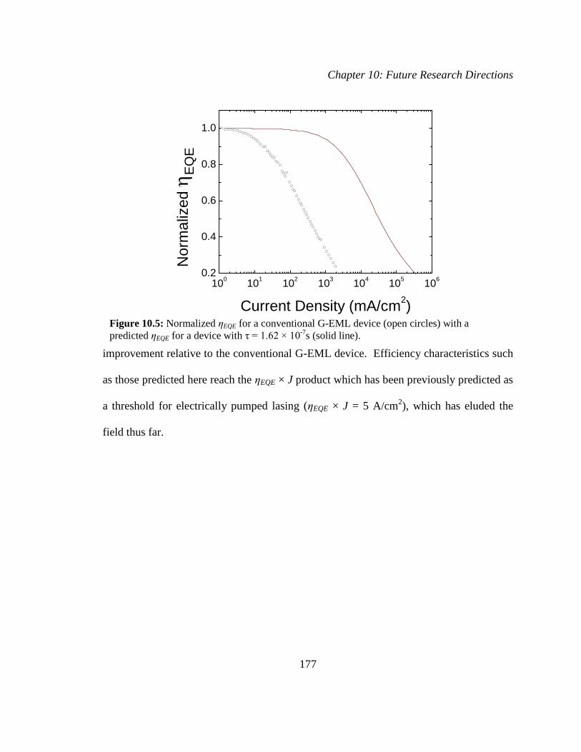
Chapter 10: Future Research Directions
177
improvement relative to the conventional G-EML device. Efficiency characteristics such
as those predicted here reach the ηEQE × J product which has been previously predicted as
a threshold for electrically pumped lasing (ηEQE × J = 5 A/cm2), which has eluded the
field thus far.
Figure 10.5: Normalized ηEQE for a conventional G-EML device (open circles) with a
predicted ηEQE for a device with τ = 1.62 × 10⁻⁷
s (solid line).
100
101
102
103
104
105
106
0.2
0.4
0.6
0.8
1.0
No
rma
lize
d
EQ
E
Current Density (mA/cm2)

Bibliography
178
Chapter 11 - Bibliography
(1) Pope, M.; Swenberg, C. E. Electronic Processes in Organic Crystals. (Oxford
University Press, 1982). 1,
(2) Pilar, F. L. Molecular Quantum Mechanics, 2nd Edition (Atkins, P. W.). J. Chem.
Educ. 1984, 61, A248
(3) Ishii, H.; Sugiyama, K.; Ito, E.; Seki, K. Energy Level Alignment and Interfacial
Electronic Structures at Organic/Metal and Organic/Organic Interfaces. Adv.
Mater. 1999, 11, 605–625
(4) Djurovich, P. I.; Mayo, E. I.; Forrest, S. R.; Thompson, M. E. Measurement of the
lowest unoccupied molecular orbital energies of molecular organic
semiconductors. Org. Electron. 2009, 10, 515–520
(5) Tadayyon, S. M.; Grandin, H. M.; Griffiths, K.; Coatsworth, L. L.; Norton, P. R.;
Aziz, H.; Popovic, Z. D. Reliable and reproducible determination of work function
and ionization potentials of layers and surfaces relevant to organic light emitting
diodes. Org. Electron. 2004, 5, 199–205
(6) Eisenschitz, R.; London, F. Über das Verhältnis der van der Waalsschen Kräfte zu
den homöopolaren Bindungskräften. Z. Für Phys. 1930, 60, 491–527
(7) Forrest, S. R. The path to ubiquitous and low-cost organic electronic appliances on
plastic. Nature 2004, 428, 911–918
(8) Hack, M.; Chwang, A.; Tung, Y.-J.; Hewitt, R.; Brown, J.; Lu, J.; Shih, C.; Ho, J.;
Street, R. A.; Moro, L.; Chu, X.; Krajewski, T.; Rutherford, N.; Visser, R. Status
and Opportunities for High Efficiency OLED Displays on Flexible Substrates.
Mater Res Soc Symp Proc 2005, 870E, H3.1.1
(9) Turro, N. J. Modern Molecular Photochemistry. (University Science Books,
1991). 1,
(10) Choi, S.; Jortner, J.; Rice, S. A.; Silbey, R. Charge‐Transfer Exciton States in
Aromatic Molecular Crystals. J. Chem. Phys. 1964, 41, 3294–3306
(11) Pope, M.; Burgos, J.; Giachino, J. Charge‐Transfer Exciton State and Energy
Levels in Tetracene Crystal. J. Chem. Phys. 1965, 43, 3367–3371
(12) Kittel, C. Introduction to Solid State Physics. (Wiley, 2004). at
<http://books.google.com/books?id=kym4QgAACAAJ>
(13) Baldo, M. A.; O’Brien, D. F.; You, Y.; Shoustikov, A.; Sibley, S.; Thompson, M.
E.; Forrest, S. R. Highly efficient phosphorescent emission from organic
electroluminescent devices. Nature 1998, 395, 151–154
(14) Baldo, M. A.; Adachi, C.; Forrest, S. R. Transient analysis of organic
electrophosphorescence. II. Transient analysis of triplet-triplet annihilation. Phys.
Rev. B 2000, 62, 10967
(15) Reineke, S.; Walzer, K.; Leo, K. Triplet-exciton quenching in organic
phosphorescent light-emitting diodes with Ir-based emitters. Phys. Rev. B 2007,
75, 125328
Bibliography
179
(16) Holmes, R. J.; Forrest, S. R.; Tung, Y.-J.; Kwong, R. C.; Brown, J. J.; Garon, S.;
Thompson, M. E. Blue organic electrophosphorescence using exothermic host–
guest energy transfer. Appl. Phys. Lett. 2003, 82, 2422–2424
(17) Holmes, R. J.; Forrest, S. R.; Sajoto, T.; Tamayo, A.; Djurovich, P. I.; Thompson,
M. E. Reduced geminate recombination in iridium-based electrophosphorescent
materials. Org. Electron. Phys. Mater. Appl. 2006, 7, 163–172
(18) Baldo, M. A.; O’Brien, D. F.; Thompson, M. E.; Forrest, S. R. The excitonic
singlet-triplet ratio in a semiconducting organic thin film. Phys Rev B 1999, 60,
14422–14428
(19) Segal, M.; Baldo, M. A.; Holmes, R. J.; Forrest, S. R.; Soos, Z. G. Excitonic
singlet-triplet ratios in molecular and polymeric organic materials. Phys. Rev. B
2003, 68, 075211
(20) Kasha, M. Characterization of electronic transitions in complex molecules. Discuss
Faraday Soc 1950, 9, 14–19
(21) Baldo, M. A.; Thompson, M. E.; Forrest, S. R. High-efficiency fluorescent organic
light-emitting devices using a phosphorescent sensitizer. Nature 2000, 403, 750–
753
(22) Okumoto, K.; Kanno, H.; Hamaa, Y.; Takahashi, H.; Shibata, K. Green fluorescent
organic light-emitting device with external quantum efficiency of nearly 10%.
Appl. Phys. Lett. 2006, 89
(23) Lamansky, S.; Djurovich, P.; Murphy, D.; Abdel-Razzaq, F.; Lee, H.-E.; Adachi,
C.; Burrows, P. E.; Forrest, S. R.; Thompson, M. E. Highly Phosphorescent Bis-
Cyclometalated Iridium Complexes: Synthesis, Photophysical Characterization,
and Use in Organic Light Emitting Diodes. J. Am. Chem. Soc. 2001, 123, 4304–
4312
(24) Kawamura, Y.; Goushi, K.; Brooks, J.; Brown, J. J.; Sasabe, H.; Adachi, C. 100%
phosphorescence quantum efficiency of Ir(III) complexes in organic
semiconductor films. Appl. Phys. Lett. 2005, 86, 071104–3
(25) Adachi, C.; Baldo, M. A.; Thompson, M. E.; Forrest, S. R. Nearly 100% internal
phosphorescence efficiency in an organic light-emitting device. J. Appl. Phys.
2001, 90, 5048–5051
(26) Förster, T. Transfer mechanisms of electronic excitation. Discuss Faraday Soc
1959, 27, 7–17
(27) Schober, M.; Anderson, M.; Thomschke, M.; Widmer, J.; Furno, M.; Scholz, R.;
Lüssem, B.; Leo, K. Quantitative description of charge-carrier transport in a white
organic light-emitting diode. Phys. Rev. B 2011, 84, 165326
(28) Bässler, H. Charge Transport in Disordered Organic Photoconductors a Monte
Carlo Simulation Study. Phys. Status Solidi B 1993, 175, 15–56
(29) Wright, J. D. Molecular Crystals. (Cambridge University Press, 1995). at
<http://books.google.com/books?id=7sroAgMASIEC>
(30) Duggal, A. R.; Heller, C.; Shiang, J. J.; Liu, J.; Lewis, L. Solution-Processed
Organic Light-Emitting Diodes for Lighting. J Disp. Technol 2007, 3, 184–192

Bibliography
180
(31) Shtein, M.; Peumans, P.; Benziger, J. B.; Forrest, S. R. Direct mask-free patterning
of molecular organic semiconductors using organic vapor jet printing. J. Appl.
Phys. 2004, 96, 4500–4507
(32) D’Andrade, B. W.; Forrest, S. R. White Organic Light-Emitting Devices for Solid-
State Lighting. Adv. Mater. 2004, 16, 1585–1595
(33) Jain, K.; Klosner, M.; Zemel, M.; Raghunandan, S. Flexible Electronics and
Displays: High-Resolution, Roll-to-Roll, Projection Lithography and Photoablation
Processing Technologies for High-Throughput Production. Proc. IEEE 2005, 93,
1500–1510
(34) Zakhidov, A. A.; Lee, J.-K.; Fong, H. H.; DeFranco, J. A.; Chatzichristidi, M.;
Taylor, P. G.; Ober, C. K.; Malliaras, G. G. Hydrofluoroethers as Orthogonal
Solvents for the Chemical Processing of Organic Electronic Materials. Adv. Mater.
2008, 20, 3481–3484
(35) Muller, C. D.; Falcou, A.; Reckefuss, N.; Rojahn, M.; Wiederhirn, V.; Rudati, P.;
Frohne, H.; Nuyken, O.; Becker, H.; Meerholz, K. Multi-colour organic light-
emitting displays by solution processing. Nature 2003, 421, 829–833
(36) Marheineke, B. OVPD: OLED manufacturing coming of age. in (2005). 5961,
596101–596101–13
(37) Baldo, M. A.; Kozlov, V. G.; Burrows, P. E.; Forrest, S. R.; Ban, V. S.; Koene, B.;
Thompson, M. E. Low pressure organic vapor phase deposition of small molecular
weight organic light emitting device structures. Appl. Phys. Lett. 1997, 71, 3033–
3035
(38) Forrest, S. R. Ultrathin Organic Films Grown by Organic Molecular Beam
Deposition and Related Techniques. Chem. Rev. 1997, 97, 1793–1896
(39) Sauerbrey, G. Verwendung von Schwingquarzen zur Wägung dünner Schichten
und zur Mikrowägung. Z. Für Phys. 1959, 155, 206–222
(40) Martin, S. J.; Granstaff, V. E.; Frye, G. C. Characterization of a quartz crystal
microbalance with simultaneous mass and liquid loading. Anal. Chem. 1991, 63,
2272–2281
(41) Oyamada, T.; Maeda, C.; Sasabe, H.; Adachi, C. Efficient Electron Injection
Mechanism in Organic Light-Emitting Diodes Using an Ultra Thin Layer of Low-
Work-Function Metals. Jpn. J. Appl. Phys. 2003, 42, L1535–L1538
(42) Hung, L. S.; Tang, C. W.; Mason, M. G. Enhanced electron injection in organic
electroluminescence devices using an Al/LiF electrode. Appl. Phys. Lett. 1997, 70,
152–154
(43) Park, S. Y.; Lee, C. H.; Song, W. J.; Seoul, C. Enhanced electron injection in
organic light-emitting devices using Al/LiF electrodes. Curr. Appl. Phys. 2001, 1,
116 – 120
(44) Hung, L. S.; Tang, C. W.; Mason, M. G.; Raychaudhuri, P.; Madathil, J.
Application of an ultrathin LiF/Al bilayer in organic surface-emitting diodes. Appl.
Phys. Lett. 2001, 78, 544–546

Bibliography
181
(45) Wang, X. J.; Zhao, J. M.; Zhou, Y. C.; Wang, X. Z.; Zhang, S. T.; Zhan, Y. Q.;
Xu, Z.; Ding, H. J.; Zhong, G. Y.; Shi, H. Z.; Xiong, Z. H.; Liu, Y.; Wang, Z. J.;
Obbard, E. G.; Ding, X. M.; Huang, W.; Hou, X. Y. Enhancement of electron
injection in organic light-emitting devices using an Ag/LiF cathode. J. Appl. Phys.
2004, 95, 3828–3830
(46) Rusu, P. C.; Giovannetti, G.; Weijtens, C.; Coehoorn, R.; Brocks, G. First-
principles study of the dipole layer formation at metal-organic interfaces. Phys Rev
B 2010, 81, 125403
(47) Heil, H.; Steiger, J.; Karg, S.; Gastel, M.; Ortner, H.; Seggern, H. Von; StoBel, M.
Mechanisms of injection enhancement in organic light-emitting diodes through an
Al/LiF electrode. J. Appl. Phys. 2001, 89, 420–424
(48) Forrest, S. R.; Bradley, D. D. C.; Thompson, M. E. Measuring the Efficiency of
Organic Light-Emitting Devices. Adv. Mater. 2003, 15, 1043–1048
(49) Endo, A.; Ogasawara, M.; Takahashi, A.; Yokoyama, D.; Kato, Y.; Adachi, C.
Thermally Activated Delayed Fluorescence from Sn4+–Porphyrin Complexes and
Their Application to Organic Light Emitting Diodes — A Novel Mechanism for
Electroluminescence. Adv. Mater. 2009, 21, 4802–4806
(50) Zhang, Q.; Li, J.; Shizu, K.; Huang, S.; Hirata, S.; Miyazaki, H.; Adachi, C. Design
of Efficient Thermally Activated Delayed Fluorescence Materials for Pure Blue
Organic Light Emitting Diodes. J. Am. Chem. Soc. 2012, 134, 14706–14709
(51) Dias, F. B.; Bourdakos, K. N.; Jankus, V.; Moss, K. C.; Kamtekar, K. T.; Bhalla,
V.; Santos, J.; Bryce, M. R.; Monkman, A. P. Triplet Harvesting with 100%
Efficiency by Way of Thermally Activated Delayed Fluorescence in Charge
Transfer OLED Emitters. Adv. Mater. 2013, 25, 3707–3714
(52) Helfrich, W.; Schneider, W. G. Recombination Radiation in Anthracene Crystals.
Phys. Rev. Lett. 1965, 14, 229–231
(53) Tang, C. W.; VanSlyke, S. A. Organic electroluminescent diodes. Appl. Phys. Lett.
1987, 51, 913–915
(54) Chen, C. H.; Tang, C. W.; Shi, J.; Klubeck, K. P. Improved red dopants for organic
electroluminescent devices. Macromol Symp 1997, 125, 49–58
(55) Adachi, C.; Thompson, M. E.; Forrest, S. R. Architectures for efficient
electrophosphorescent organic light-emitting devices. Sel. Top. Quantum Electron.
IEEE J. Of 2002, 8, 372–377
(56) O’Brien, D. F.; Baldo, M. A.; Thompson, M. E.; Forrest, S. R. Improved energy
transfer in electrophosphorescent devices. Appl. Phys. Lett. 1999, 74, 442–444
(57) Baldo, M. A.; Lamansky, S.; Burrows, P. E.; Thompson, M. E.; Forrest, S. R. Very
high-efficiency green organic light-emitting devices based on
electrophosphorescence. Appl. Phys. Lett. 1999, 75, 4–6
(58) Tanaka, D.; Sasabe, H.; Li, Y.-J.; Su, S.-J.; Takeda, T.; Kido, J. Ultra high
efficiency green organic light-emitting devices. Jpn. J. Appl. Phys. Part 2-Lett.
Express Lett. 2007, 46, L10–L12

Bibliography
182
(59) He, G.; Schneider, O.; Qin, D.; Zhou, X.; Pfeiffer, M.; Leo, K. Very high-
efficiency and low voltage phosphorescent organic light-emitting diodes based on
a p-i-n junction. J. Appl. Phys. 2004, 95, 5773–5777
(60) Chopra, N.; Lee, J.; Zheng, Y.; Eom, S.-H.; Xue, J.; So, F. High efficiency blue
phosphorescent organic light-emitting device. Appl. Phys. Lett. 2008, 93, 143307–
3
(61) Watanabe, S.; Ide, N.; Kido, J. High-Efficiency Green Phosphorescent Organic
Light-Emitting Devices with Chemically Doped Layers. Jpn. J. Appl. Phys. 2007,
46, 1186
(62) D’Andrade, B. W.; Holmes, R. J.; Forrest, S. R. Efficient Organic
Electrophosphorescent White-Light-Emitting Device with a Triple Doped
Emissive Layer. Adv. Mater. 2004, 16, 624–628
(63) Sun, Y.; Forrest, S. R. High-efficiency white organic light emitting devices with
three separate phosphorescent emission layers. Appl. Phys. Lett. 2007, 91, 263503–
3
(64) Reineke, S.; Lindner, F.; Schwartz, G.; Seidler, N.; Walzer, K.; Lüssem, B.; Leo,
K. White organic light-emitting diodes with fluorescent tube efficiency. Nature
2009, 459, 234–238
(65) Xin, Q.; Li, W. L.; Su, W. M.; Li, T. L.; Su, Z. S.; Chu, B.; Li, B. Emission
mechanism in organic light-emitting devices comprising a europium complex as
emitter and an electron transporting material as host. J. Appl. Phys. 2007, 101
(66) Lee, J.; Lee, J.-I.; Song, K.-I.; Lee, S. J.; Chu, H. Y. Effects of interlayers on
phosphorescent blue organic light-emitting diodes. Appl. Phys. Lett. 2008, 92
(67) Tanaka, I.; Tabata, Y.; Tokito, S. Förster and Dexter energy-transfer processes in
fluorescent BAlq thin films doped with phosphorescent Ir(ppy)3 molecules. J.
Appl. Phys. 2006, 99, -
(68) Hung, W.-Y.; Chen, Z.-W.; You, H.-W.; Fan, F.-C.; Chen, H.-F.; Wong, K.-T.
Efficient carrier- and exciton-confining device structure that enhances blue
PhOLED efficiency and reduces efficiency roll-off. Org. Electron. 2011, 12, 575 –
581
(69) Holmes, R. J.; D’Andrade, B. W.; Forrest, S. R.; Ren, X.; Li, J.; Thompson, M. E.
Efficient, deep-blue organic electrophosphorescence by guest charge trapping.
Appl. Phys. Lett. 2003, 83, 3818–3820
(70) Polikarpov, E.; Swensen, J. S.; Chopra, N.; So, F.; Padmaperuma, A. B. An
ambipolar phosphine oxide-based host for high power efficiency blue
phosphorescent organic light emitting devices. Appl. Phys. Lett. 2009, 94, -
(71) Chaskar, A.; Chen, H.-F.; Wong, K.-T. Bipolar Host Materials: A Chemical
Approach for Highly Efficient Electrophosphorescent Devices. Adv. Mater. 2011,
23, 3876–3895
(72) Qiao, X.; Tao, Y.; Wang, Q.; Ma, D.; Yang, C.; Wang, L.; Qin, J.; Wang, F.
Controlling charge balance and exciton recombination by bipolar host in single-
layer organic light-emitting diodes. J. Appl. Phys. 2010, 108, 034508–8

Bibliography
183
(73) Solid-State Lighting Research and Development: Multi-Year Program Plan. (U.S.
Department of Energy, 2013). 1–89
(74) Cho, T.-Y.; Lin, C.-L.; Wu, C.-C. Microcavity two-unit tandem organic light-
emitting devices having a high efficiency. Appl. Phys. Lett. 2006, 88, 111106–3
(75) Kanno, H.; Holmes, R. J.; Sun, Y.; Kena-Cohen, S.; Forrest, S. R. White Stacked
Electrophosphorescent Organic Light-Emitting Devices Employing MoO3 as a
Charge-Generation Layer. Adv. Mater. 2006, 18, 339–342
(76) Yan, F.; Wei Sun, X. A plasmonically enhanced charge generation layer for
tandem organic light emitting device. Appl. Phys. Lett. 2013, 102, -
(77) D’Andrade, B.; Forrest, S. R. Formation of triplet excimers and dimers in
amorphous organic thin films and light emitting devices. Chem. Phys. 2003, 286,
321 – 335
(78) Williams, E. L.; Haavisto, K.; Li, J.; Jabbour, G. E. Excimer-Based White
Phosphorescent Organic Light-Emitting Diodes with Nearly 100 % Internal
Quantum Efficiency. Adv. Mater. 2007, 19, 197–202
(79) Chopra, N.; Swensen, J. S.; Polikarpov, E.; Cosimbescu, L.; So, F.; Padmaperuma,
A. B. High efficiency and low roll-off blue phosphorescent organic light-emitting
devices using mixed host architecture. Appl. Phys. Lett. 2010, 97, 033304–3
(80) He, G.; Pfeiffer, M.; Leo, K.; Hofmann, M.; Birnstock, J.; Pudzich, R.; Salbeck, J.
High-efficiency and low-voltage p-i-n electrophosphorescent organic light-
emitting diodes with double-emission layers. Appl. Phys. Lett. 2004, 85, 3911–
3913
(81) Lee, J.; Lee, J.-I.; Lee, J. Y.; Chu, H. Y. Enhanced efficiency and reduced roll-off
in blue and white phosphorescent organic light-emitting diodes with a mixed host
structure. Appl. Phys. Lett. 2009, 94, 193305–3
(82) Murawski, C.; Leo, K.; Gather, M. C. Efficiency Roll-Off in Organic Light-
Emitting Diodes. Adv. Mater. 2013, 25, 6801–6827
(83) Adachi, C.; Baldo, M. A.; Forrest, S. R.; Thompson, M. E. High-efficiency organic
electrophosphorescent devices with tris(2-phenylpyridine)iridium doped into
electron-transporting materials. Appl. Phys. Lett. 2000, 77, 904–906
(84) Liu, S. W.; Huang, C. A.; Lee, J. H.; Yang, K. H.; Chen, C. C.; Chang, Y. Blue
mixed host organic light emitting devices. Proc. Symp. H Photonic Process. Surf.
Thin Films Devices E-MRS 2003 Spring Conf. 2004, 453–454, 312–315
(85) Lee, J.; Lee, J.-I.; Song, K.-I.; Lee, S. J.; Chu, H. Y. Influence of doping profile on
the efficiency of blue phosphorescent organic light-emitting diodes. Appl. Phys.
Lett. 2008, 92, 133304–3
(86) Lee, M.-T.; Lin, J.-S.; Chu, M.-T.; Tseng, M.-R. Suppression of efficiency roll off
in blue phosphorescent organic light-emitting devices using double emission layers
with additional carrier-transporting material. Appl. Phys. Lett. 2009, 94, 083506–3
(87) Zhou, X.; Qin, D. S.; Pfeiffer, M.; Blochwitz-Nimoth, J.; Werner, A.; Drechsel, J.;
Maennig, B.; Leo, K.; Bold, M.; Erk, P.; Hartmann, H. High-efficiency

Bibliography
184
electrophosphorescent organic light-emitting diodes with double light-emitting
layers. Appl. Phys. Lett. 2002, 81, 4070–4072
(88) Lee, J.-H.; Wu, C.-I.; Liu, S.-W.; Huang, C.-A.; Chang, Y. Mixed host organic
light-emitting devices with low driving voltage and long lifetime. Appl. Phys. Lett.
2005, 86, 103506–3
(89) Kondakova, M. E.; Pawlik, T. D.; Young, R. H.; Giesen, D. J.; Kondakov, D. Y.;
Brown, C. T.; Deaton, J. C.; Lenhard, J. R.; Klubek, K. P. High-efficiency, low-
voltage phosphorescent organic light-emitting diode devices with mixed host. J.
Appl. Phys. 2008, 104, 094501–17
(90) Matsushima, T.; Adachi, C. Suppression of exciton annihilation at high current
densities in organic light-emitting diode resulting from energy-level alignments of
carrier transport layers. Appl. Phys. Lett. 2008, 92, 063306–3
(91) Zhao, Y.; Chen, J.; Chen, W.; Ma, D. Poly(3,4-
ethylenedioxythiophene):poly(styrenesulfonate)/MoO3 composite layer for
efficient and stable hole injection in organic semiconductors. J. Appl. Phys. 2012,
111
(92) Koch, N.; Duhm, S.; Rabe, J. P.; Vollmer, A.; Johnson, R. L. Optimized Hole
Injection with Strong Electron Acceptors at Organic-Metal Interfaces. Phys. Rev.
Lett. 2005, 95, 237601
(93) Zhou, X.; Pfeiffer, M.; Blochwitz, J.; Werner, A.; Nollau, A.; Fritz, T.; Leo, K.
Very-low-operating-voltage organic light-emitting diodes using a p-doped
amorphous hole injection layer. Appl. Phys. Lett. 2001, 78, 410–412
(94) Hwu, T.-Y.; Tsai, T.-C.; Hung, W.-Y.; Chang, S.-Y.; Chi, Y.; Chen, M.-H.; Wu,
C.-I.; Wong, K.-T.; Chia, L.-C. An electron-transporting host material compatible
with diverse tripletemitters used for highly efficient red- and green-
electrophosphorescentdevices. Chem Commun 2008, 4956
(95) Olthof, S.; Meerheim, R.; Schober, M.; Leo, K. Energy level alignment at the
interfaces in a multilayer organic light-emitting diode structure. Phys. Rev. B 2009,
79, 245308
(96) Naka, S.; Okada, H.; Onnagawa, H.; Tsutsui, T. High electron mobility in
bathophenanthroline. Appl. Phys. Lett. 2000, 76, 197–199
(97) Kang, J.-W.; Lee, S.-H.; Park, H.-D.; Jeong, W.-I.; Yoo, K.-M.; Park, Y.-S.; Kim,
J.-J. Low roll-off of efficiency at high current density in phosphorescent organic
light emitting diodes. Appl. Phys. Lett. 2007, 90, 223508–3
(98) Hsiao, C.-H.; Chen, Y.-H.; Lin, T.-C.; Hsiao, C.-C.; Lee, J.-H. Recombination
zone in mixed-host organic light-emitting devices. Appl. Phys. Lett. 2006, 89,
163511–3
(99) Liu, Z. W.; Helander, M. G.; Wang, Z. B.; Lu, Z. H. Efficient bilayer
phosphorescent organic light-emitting diodes: Direct hole injection into triplet
dopants. Appl. Phys. Lett. 2009, 94, 113305–3
(100) Reineke, S.; Thomschke, M.; Lüssem, B.; Leo, K. White organic light-emitting
diodes: Status and perspective. Rev. Mod. Phys. 2013, 85, 1245–1293

Bibliography
185
(101) Sasabe, H.; Takamatsu, J.; Motoyama, T.; Watanabe, S.; Wagenblast, G.; Langer,
N.; Molt, O.; Fuchs, E.; Lennartz, C.; Kido, J. High-Efficiency Blue and White
Organic Light-Emitting Devices Incorporating a Blue Iridium Carbene Complex.
Adv. Mater. 2010, 22, 5003–5007
(102) Wu, C.-C.; Lin, Y.-T.; Wong, K.-T.; Chen, R.-T.; Chien, Y.-Y. Efficient Organic
Blue-Light-Emitting Devices with Double Confinement on Terfluorenes with
Ambipolar Carrier Transport Properties. Adv. Mater. 2004, 16, 61–65
(103) Su, S.-J.; Gonmori, E.; Sasabe, H.; Kido, J. Highly Efficient Organic Blue-and
White-Light-Emitting Devices Having a Carrier- and Exciton-Confining Structure
for Reduced Efficiency Roll-Off. Adv. Mater. 2008, 20, 4189–4194
(104) Chan, M. Y.; Lee, C. S.; Lai, S. L.; Fung, M. K.; Wong, F. L.; Sun, H. Y.; Lau, K.
M.; Lee, S. T. Efficient organic photovoltaic devices using a combination of
exciton blocking layer and anodic buffer layer. J. Appl. Phys. 2006, 100, -
(105) Cai, X.; Padmaperuma, A. B.; Sapochak, L. S.; Vecchi, P. A.; Burrows, P. E.
Electron and hole transport in a wide bandgap organic phosphine oxide for blue
electrophosphorescence. Appl. Phys. Lett. 2008, 92, -
(106) Tang, C. W.; VanSlyke, S. A.; Chen, C. H. Electroluminescence of doped organic
thin films. J. Appl. Phys. 1989, 65, 3610–3616
(107) Huang, J.; Pfeiffer, M.; Werner, A.; Blochwitz, J.; Leo, K.; Liu, S. Low-voltage
organic electroluminescent devices using pin structures. Appl. Phys. Lett. 2002, 80,
139–141
(108) Chen, Y.-Y.; Yu, B.-Y.; Wang, W.-B.; Hsu, M.-F.; Lin, W.-C.; Lin, Y.-C.; Jou, J.-
H.; Shyue, J.-J. X-ray Photoelectron Spectrometry Depth Profiling of Organic Thin
Films Using C60 Sputtering. Anal. Chem. 2007, 80, 501–505
(109) Ninomiya, S.; Ichiki, K.; Yamada, H.; Nakata, Y.; Seki, T.; Aoki, T.; Matsuo, J.
Molecular depth profiling of multilayer structures of organic semiconductor
materials by secondary ion mass spectrometry with large argon cluster ion beams.
Rapid Commun. Mass Spectrom. 2009, 23, 3264–3268
(110) Yu, B.-Y.; Chen, Y.-Y.; Wang, W.-B.; Hsu, M.-F.; Tsai, S.-P.; Lin, W.-C.; Lin,
Y.-C.; Jou, J.-H.; Chu, C.-W.; Shyue, J.-J. Depth Profiling of Organic Films with
X-ray Photoelectron Spectroscopy Using C60+ and Ar+ Co-Sputtering. Anal.
Chem. 2008, 80, 3412–3415
(111) Kim, S. H.; Jang, J.; Lee, J. Y. Relationship between host energy levels and device
performances of phosphorescent organic light-emitting diodes with triplet mixed
host emitting structure. Appl. Phys. Lett. 2007, 91, 083511–3
(112) Liu, S.-W.; Lee, J.-H.; Lee, C.-C.; Chen, C.-T.; Wang, J.-K. Charge carrier
mobility of mixed-layer organic light-emitting diodes. Appl. Phys. Lett. 2007, 91,
142106–3
(113) Erickson, N. C.; Holmes, R. J. Highly efficient, single-layer organic light-emitting
devices based on a graded-composition emissive layer. Appl. Phys. Lett. 2010, 97,
083308–3

Bibliography
186
(114) Wang, J.; Shi, X.; Liu, J.; Huang, S.; Wu, X.; Ye, Z.; Lu, J.; Su, Y.; He, G. P.110:
High-Efficiency OLEDs Based on the Gradient Doping in Transporting Layers.
SID Symp. Dig. Tech. Pap. 2013, 44, 1400–1402
(115) Erickson, N. C.; Holmes, R. J. Relating charge transport and performance in
single-layer graded-composition organic light-emitting devices. J. Appl. Phys.
2011, 110, 084515–8
(116) Shard, A. G.; Brewer, P. J.; Green, F. M.; Gilmore, I. S. Measurement of sputtering
yields and damage in C60 SIMS depth profiling of model organic materials. Surf.
Interface Anal. 2007, 39, 294–298
(117) Ninomiya, S.; Ichiki, K.; Yamada, H.; Nakata, Y.; Seki, T.; Aoki, T.; Matsuo, J.
Precise and fast secondary ion mass spectrometry depth profiling of polymer
materials with large Ar cluster ion beams. Rapid Commun. Mass Spectrom. 2009,
23, 1601–1606
(118) Miyayama, T.; Sanada, N.; Suzuki, M.; Hammond, J. S.; Si, S.-Q. D.; Takahara, A.
X-ray photoelectron spectroscopy study of polyimide thin films with Ar cluster ion
depth profiling. J. Vac. Sci. Technol. A 2010, 28, L1–L4
(119) Grunthaner, F. J. Fundamentals of X-Ray Photoemission Spectroscopy. MRS Bull.
1987, 12, 60–64
(120) Scott, J. C.; Malliaras, G. G. Charge injection and recombination at the metal–
organic interface. Chem. Phys. Lett. 1999, 299, 115–119
(121) Wang, Z. B.; Helander, M. G.; Greiner, M. T.; Qiu, J.; Lu, Z. H. Carrier mobility
of organic semiconductors based on current-voltage characteristics. J. Appl. Phys.
2010, 107, 034506
(122) Frenkel, J. On Pre-Breakdown Phenomena in Insulators and Electronic Semi-
Conductors. Phys. Rev. 1938, 54, 647
(123) Blom, P. W. M.; Jong, M. J. M. de; Munster, M. G. van. Electric-field and
temperature dependence of the hole mobility in poly(p-phenylene vinylene). Phys.
Rev. B 1997, 55, R656
(124) Gill, W. D. Drift mobilities in amorphous charge-transfer complexes of
trinitrofluorenone and poly-n-vinylcarbazole. J. Appl. Phys. 1972, 43, 5033–5040
(125) Rakhmanova, S. V.; Conwell, E. M. Electric-field dependence of mobility in
conjugated polymer films. Appl. Phys. Lett. 2000, 76, 3822–3824
(126) Bozano, L.; Carter, S. A.; Scott, J. C.; Malliaras, G. G.; Brock, P. J. Temperature-
and field-dependent electron and hole mobilities in polymer light-emitting diodes.
Appl. Phys. Lett. 1999, 74, 1132–1134
(127) Zhang, X.-W.; Khan, M. A.; Jiang, X.-Y.; Cao, J.; Zhu, W.-Q.; Zhang, Z.-L.
Electron injection property at the organic–metal interface in organic light-emitting
devices revealed by current–voltage characteristics. Phys. B Condens. Matter
2009, 404, 1247–1250
(128) Wong, T. C.; Kovac, J.; Lee, C. S.; Hung, L. S.; Lee, S. T. Transient
electroluminescence measurements on electron-mobility of N-arylbenzimidazoles.
Chem. Phys. Lett. 2001, 334, 61–64

Bibliography
187
(129) Giebink, N. C.; Forrest, S. R. Quantum efficiency roll-off at high brightness in
fluorescent and phosphorescent organic light emitting diodes. Phys. Rev. B 2008,
77, 235215
(130) Kalinowski, J.; Stampor, W.; Mȩżyk, J.; Cocchi, M.; Virgili, D.; Fattori, V.;
Marco, P. Di. Quenching effects in organic electrophosphorescence. Phys. Rev. B
2002, 66, 235321
(131) Kalinowski, J.; Stampor, W.; Szmytkowski, J.; Virgili, D.; Cocchi, M.; Fattori, V.;
Sabatini, C. Coexistence of dissociation and annihilation of excitons on charge
carriers in organic phosphorescent emitters. Phys. Rev. B 2006, 74, 085316
(132) Rand, B. P.; Xue, J.; Uchida, S.; Forrest, S. R. Mixed donor-acceptor molecular
heterojunctions for photovoltaic applications. I. Material properties. J. Appl. Phys.
2005, 98, 124902–7
(133) Hobson, P. A.; Wedge, S.; Wasey, J. A. E.; Sage, I.; Barnes, W. L. Surface
Plasmon Mediated Emission from Organic Light-Emitting Diodes. Adv. Mater.
2002, 14, 1393–1396
(134) Smith, L. H.; Wasey, J. A. E.; Barnes, W. L. Light outcoupling efficiency of top-
emitting organic light-emitting diodes. Appl. Phys. Lett. 2004, 84, 2986–2988
(135) Cho, J. H.; Lee, J.; Xia, Y.; Kim, B.; He, Y.; Renn, M. J.; Lodge, T. P.; Frisbie, C.
D. Printable ion-gel gate dielectrics for low-voltage polymer thin-film transistors
on plastic. Nat. Mater. 2008, 7, 900–906
(136) Lee, J.; Kaake, L. G.; Cho, J. H.; Zhu, X.-Y.; Lodge, T. P.; Frisbie, C. D. Ion gel-
gated polymer thin-film transistors: operating mechanism and characterization of
gate dielectric capacitance, switching speed, and stability. J. Phys. Chem. C 2009,
113, 8972–8981
(137) Xia, Y.; Zhang, W.; Ha, M.; Cho, J. H.; Renn, M. J.; Kim, C. H.; Frisbie, C. D.
Printed Sub-2 V Gel-Electrolyte-Gated Polymer Transistors and Circuits. Adv.
Funct. Mater. 2010, 20, 587–594
(138) Braga, D.; Ha, M.; Xie, W.; Frisbie, C. D. Ultralow contact resistance in
electrolyte-gated organic thin film transistors. Appl. Phys. Lett. 2010, 97, 193311–
193311
(139) Herlogsson, L.; Noh, Y.-Y.; Zhao, N.; Crispin, X.; Sirringhaus, H.; Berggren, M.
Downscaling of Organic Field-Effect Transistors with a Polyelectrolyte Gate
Insulator. Adv. Mater. 2008, 20, 4708–4713
(140) Chabinyc, M. L.; Salleo, A. Materials Requirements and Fabrication of Active
Matrix Arrays of Organic Thin-Film Transistors for Displays. Chem. Mater. 2004,
16, 4509–4521
(141) Meyer, J.; Hamwi, S.; Bulow, T.; Johannes, H.-H.; Riedl, T.; Kowalsky, W.
Highly efficient simplified organic light emitting diodes. Appl. Phys. Lett. 2007,
91, 113506–3
(142) Jeon, W. S.; Park, T. J.; Kim, K. H.; Pode, R.; Jang, J.; Kwon, J. H. High
efficiency red phosphorescent organic light-emitting diodes with single layer
structure. Org. Electron. 2010, 11, 179–183

Bibliography
188
(143) Furno, M.; Meerheim, R.; Hofmann, S.; Lüssem, B.; Leo, K. Efficiency and rate of
spontaneous emission in organic electroluminescent devices. Phys. Rev. B 2012,
85, 115205
(144) Park, I.-S.; Park, S.-R.; Shin, D.-Y.; Oh, J.-S.; Song, W.-J.; Yoon, J.-H. Modeling
and simulation of electronic and excitonic emission properties in organic host–
guest systems. Org. Electron. 2010, 11, 218–226
(145) Bulović, V.; Khalfin, V. B.; Gu, G.; Burrows, P. E.; Garbuzov, D. Z.; Forrest, S. R.
Weak microcavity effects in organic light-emitting devices. Phys. Rev. B 1998, 58,
3730–3740
(146) Schubert, E. F.; Hunt, N. E. J.; Micovic, M.; Malik, R. J.; Sivco, D. L.; Cho, A. Y.;
Zydzik, G. J. Highly Efficient Light-Emitting Diodes with Microcavities. Science
1994, 265, pp. 943–945
(147) Huang, Q.; Reineke, S.; Walzer, K.; Pfeiffer, M.; Leo, K. Quantum efficiency
enhancement in top-emitting organic light-emitting diodes as a result of enhanced
intrinsic quantum yield. Appl. Phys. Lett. 2006, 89, 263512–3
(148) Mladenovski, S.; Reineke, S.; Neyts, K. Measurement and simulation of exciton
decay times in organic light-emitting devices with different layer structures. Opt.
Lett. 2009, 34, 1375–1377
(149) Song, D.; Zhao, S.; Aziz, H. Modification of Exciton Lifetime by the Metal
Cathode in Phosphorescent OLEDs, and Implications on Device Efficiency and
Efficiency Roll-off Behavior. Adv. Funct. Mater. 2011, 21, 2311–2317
(150) Reineke, S.; Schwartz, G.; Walzer, K.; Leo, K. Direct observation of host-guest
triplet-triplet annihilation in phosphorescent solid mixed films. Phys. Status Solidi
RRL Rapid Res. Lett. 2009, 3, 67–69
(151) Song, D.; Zhao, S.; Luo, Y.; Aziz, H. Causes of efficiency roll-off in
phosphorescent organic light emitting devices: Triplet-triplet annihilation versus
triplet-polaron quenching. Appl. Phys. Lett. 2010, 97, 243304–3
(152) Staroske, W.; Pfeiffer, M.; Leo, K.; Hoffmann, M. Single-Step Triplet-Triplet
Annihilation: An Intrinsic Limit for the High Brightness Efficiency of
Phosphorescent Organic Light Emitting Diodes. Phys. Rev. Lett. 2007, 98, 197402
(153) Bhansali, U. S.; Jia, H.; Lopez, M. A. Q.; Gnade, B. E.; Chen, W.-H.; Omary, M.
A. Controlling the carrier recombination zone for improved color stability in a
two-dopant fluorophore/phosphor white organic light-emitting diode. Appl. Phys.
Lett. 2009, 94, 203501–3
(154) Gather, M. C.; Flammich, M.; Danz, N.; Michaelis, D.; Meerholz, K. Measuring
the profile of the emission zone in polymeric organic light-emitting diodes. Appl.
Phys. Lett. 2009, 94, 263301–3
(155) Kalinowski, J.; Palilis, L. C.; Kim, W. H.; Kafafi, Z. H. Determination of the width
of the carrier recombination zone in organic light-emitting diodes. J. Appl. Phys.
2003, 94, 7764–7767
(156) Mensfoort, S. L. M. van; Carvelli, M.; Megens, M.; Wehenkel, D.; Bartyzel, M.;
Greiner, H.; Janssen, R. A. J.; Coehoorn, R. Measuring the light emission profile in

Bibliography
189
organic light-emitting diodes with nanometre spatial resolution. Nat Photon 2010,
4, 329–335
(157) Chopra, N.; Lee, J.; Zheng, Y.; Eom, S.-H.; Xue, J.; So, F. Effect of the Charge
Balance on High-Efficiency Blue-Phosphorescent Organic Light-Emitting Diodes.
ACS Appl. Mater. Interfaces 2009, 1, 1169–1172
(158) Choi, W. H.; Cheung, C. H.; So, S. K. Can an organic phosphorescent dye act as a
charge transporter? Org. Electron. 2010, 11, 872–875
(159) Weichsel, C.; Burtone, L.; Reineke, S.; Hintschich, S. I.; Gather, M. C.; Leo, K.;
Lüssem, B. Storage of charge carriers on emitter molecules in organic light-
emitting diodes. Phys. Rev. B 2012, 86, 075204
(160) Lee, S.; Tang, C. W. Fabrication of a blue organic light-emitting diode with a
novel thermal deposition boat. J. Vac. Sci. Technol. B Microelectron. Nanometer
Struct. 2011, 29, 062401–4
(161) Staudigel, J.; Stossel, M.; Steuber, F.; Simmerer, J. A quantitative numerical model
of multilayer vapor-deposited organic light emitting diodes. J. Appl. Phys. 1999,
86, 3895–3910
(162) Neumann, F.; Genenko, Y. A.; Schmechel, R.; Seggern, H. von. Role of diffusion
on SCLC transport in double injection devices. Synth. Met. 2005, 150, 291–296
(163) Malliaras, G. G.; Scott, J. C. Numerical simulations of the electrical characteristics
and the efficiencies of single-layer organic light emitting diodes. J. Appl. Phys.
1999, 85, 7426–7432
(164) Coehoorn, R.; Mensfoort, S. L. M. van. Effects of disorder on the current density
and recombination profile in organic light-emitting diodes. Phys. Rev. B 2009, 80,
085302
(165) Noh, S.; Suman, C. K.; Hong, Y.; Lee, C. Carrier conduction mechanism for
phosphorescent material doped organic semiconductor. J. Appl. Phys. 2009, 105,
033709–5
(166) Partee, J.; Frankevich, E. L.; Uhlhorn, B.; Shinar, J.; Ding, Y.; Barton, T. J.
Delayed Fluorescence and Triplet-Triplet Annihilation in π-Conjugated Polymers.
Phys. Rev. Lett. 1999, 82, 3673–3676
(167) Yokoyama, D.; Park, Y.; Kim, B.; Kim, S.; Pu, Y.-J.; Kido, J.; Park, J. Dual
efficiency enhancement by delayed fluorescence and dipole orientation in high-
efficiency fluorescent organic light-emitting diodes. Appl. Phys. Lett. 2011, 99,
123303
(168) Popovic, Z. D.; Aziz, H. Delayed electroluminescence in small-molecule-based
organic light-emitting diodes: Evidence for triplet-triplet annihilation and
recombination-center-mediated light-generation mechanism. J. Appl. Phys. 2005,
98, 013510
(169) Kondakov, D. Y. Characterization of triplet-triplet annihilation in organic light-
emitting diodes based on anthracene derivatives. J. Appl. Phys. 2007, 102, 114504

Bibliography
190
(170) Kondakov, D. Y.; Pawlik, T. D.; Hatwar, T. K.; Spindler, J. P. Triplet annihilation
exceeding spin statistical limit in highly efficient fluorescent organic light-emitting
diodes. J. Appl. Phys. 2009, 106, 124510
(171) Uoyama, H.; Goushi, K.; Shizu, K.; Nomura, H.; Adachi, C. Highly efficient
organic light-emitting diodes from delayed fluorescence. Nature 2012, 492, 234–
238
(172) Endo, A.; Sato, K.; Yoshimura, K.; Kai, T.; Kawada, A.; Miyazaki, H.; Adachi, C.
Efficient up-conversion of triplet excitons into a singlet state and its application for
organic light emitting diodes. Appl. Phys. Lett. 2011, 98, 083302
(173) Masui, K.; Nakanotani, H.; Adachi, C. Analysis of exciton annihilation in high-
efficiency sky-blue organic light-emitting diodes with thermally activated delayed
fluorescence. Org. Electron. 2013, 14, 2721–2726
(174) Kamtekar, K. T.; Monkman, A. P.; Bryce, M. R. Recent Advances in White
Organic Light-Emitting Materials and Devices (WOLEDs). Adv. Mater. 2010, 22,
572–582
(175) Wellmann, P.; Hofmann, M.; Zeika, O.; Werner, A.; Birnstock, J.; Meerheim, R.;
He, G.; Walzer, K.; Pfeiffer, M.; Leo, K. High-efficiency p-i-n organic light-
emitting diodes with long lifetime. J. Soc. Inf. Disp. 2005, 13, 393–397
(176) Gather, M. C.; Köber, S.; Heun, S.; Meerholz, K. Improving the lifetime of white
polymeric organic light-emitting diodes. J. Appl. Phys. 2009, 106, 024506
(177) Meerheim, R.; Scholz, S.; Olthof, S.; Schwartz, G.; Reineke, S.; Walzer, K.; Leo,
K. Influence of charge balance and exciton distribution on efficiency and lifetime
of phosphorescent organic light-emitting devices. J. Appl. Phys. 2008, 104, 014510
(178) Lampert, M. A.; Marks, P. Current Injection in Solids. (Academic Press Inc,
1970). (179) Erickson, N. C.; Holmes, R. J. Investigating the Role of Emissive Layer
Architecture on the Exciton Recombination Zone in Organic Light-Emitting
Devices. Adv. Funct. Mater. 2013, 23, 5190–5198
(180) Kalinowski, J.; Mȩżyk, J.; Meinardi, F.; Tubino, R.; Cocchi, M.; Virgili, D.
Phosphorescence response to excitonic interactions in Ir organic complex-based
electrophosphorescent emitters. J. Appl. Phys. 2005, 98, 063532
(181) Kim, Y. H.; Lee, J.; Kim, W. M.; Fuchs, C.; Hofmann, S.; Chang, H.-W.; Gather,
M. C.; Müller-Meskamp, L.; Leo, K. We Want Our Photons Back: Simple
Nanostructures for White Organic Light-Emitting Diode Outcoupling. Adv. Funct.
Mater. 2013, n/a–n/a doi:10.1002/adfm.201303401
(182) Pettersson, L. A. A.; Roman, L. S.; Inganäs, O. Modeling photocurrent action
spectra of photovoltaic devices based on organic thin films. J. Appl. Phys. 1999,
86, 487–496
(183) Benisty, H.; Stanley, R.; Mayer, M. Method of source terms for dipole emission
modification in modes of arbitrary planar structures. J Opt Soc Am A 1998, 15,
1192–1201

Bibliography
191
(184) Neyts, K. A. Simulation of light emission from thin-film microcavities. J Opt Soc
Am A 1998, 15, 962–971
(185) Mladenovski, S.; Hofmann, S.; Reineke, S.; Penninck, L.; Verschueren, T.; Neyts,
K. Integrated optical model for organic light-emitting devices. J. Appl. Phys. 2011,
109, -
(186) Furno, M.; Meerheim, R.; Thomschke, M.; Hofmann, S.; Lüssem, B.; Leo, K.
Outcoupling efficiency in small-molecule OLEDs: from theory to experiment. in
(2010). 7617, 761716–761716–12
(187) Wang, Z. B.; Helander, M. G.; Xu, X. F.; Puzzo, D. P.; Qiu, J.; Greiner, M. T.; Lu,
Z. H. Optical design of organic light emitting diodes. J. Appl. Phys. 2011, 109, -
(188) D’Andrade, B. W.; Brooks, J.; Adamovich, V.; Thompson, M. E.; Forrest, S. R.
White Light Emission Using Triplet Excimers in Electrophosphorescent Organic
Light-Emitting Devices. Adv. Mater. 2002, 14, 1032–1036
(189) Han, J.; Shen, L.; Chen, X.; Fang, W. Phosphorescent mechanism for single-
dopant white OLED of FPt: electronic structure and electron exchange-induced
energy transfer. J Mater Chem C 2013, 1, 4227–4235
(190) Adamovich, V.; Brooks, J.; Tamayo, A.; Alexander, A. M.; Djurovich, P. I.;
D’Andrade, B. W.; Adachi, C.; Forrest, S. R.; Thompson, M. E. High efficiency
single dopant white electrophosphorescent light emitting diodes. New J Chem
2002, 26, 1171–1178
(191) Fleetham, T.; Ecton, J.; Wang, Z.; Bakken, N.; Li, J. Single-Doped White Organic
Light-Emitting Device with an External Quantum Efficiency Over 20%. Adv.
Mater. 2013, 25, 2573–2576
(192) D’Andrade, B. W.; Forrest, S. R. Effects of exciton and charge confinement on the
performance of white organic p−i−n electrophosphorescent emissive excimer
devices. J. Appl. Phys. 2003, 94, 3101–3109
(193) Tsai, Y.-S.; Wang, S.-H.; Chen, S.-Y.; Su, S.-Y.; Juang, F.-S. Efficiency
improvement of flexible fluorescent and phosphorescent organic light emitting
diodes by inserting a spin-coating buffer layer. 4th Int. Conf. Technol. Adv. Thin
Films Surf. Coat. 2009, 517, 5338–5342
(194) Ie, S.; Kim, J.-H.; Bae, B. T.; Park, D.-H.; Choi, J.-W.; Choi, W.-K. Amorphous
indium tin oxide electrodes for piezoelectric and light-emitting device deposited by
vacuum roll to roll process. Proc. 1st Int. Conf. Microelectron. Plasma Technol.
ICMAP 2008 2009, 517, 4015–4018
(195) Bulovic, V. Bright, saturated, red-to-yellow organic light-emitting devices based
on polarization-induced spectral shifts. Chem Phys Lett 1998, 287, 455–460
(196) Bulovic, V.; Deshpande, R.; Thompson, M. E.; Forrest, S. R. Tuning the color
emission of thin film molecular organic light emitting devices by the solid state
solvation effect. Chem Phys Lett 1999, 308, 317
(197) Grossiord, N.; Kroon, J. M.; Andriessen, R.; Blom, P. W. M. Degradation
mechanisms in organic photovoltaic devices. Org. Electron. 2012, 13, 432–456

Bibliography
192
(198) Yook, K. S.; Jeon, S. O.; Joo, C. W.; Lee, J. Y. Correlation of lifetime and
recombination zone in green phosphorescent organic light-emitting diodes. Appl.
Phys. Lett. 2009, 94, -
(199) Purcell, E. M.; Torrey, H. C.; Pound, R. V. Resonance Absorption by Nuclear
Magnetic Moments in a Solid. Phys. Rev. 1946, 69, 37–38
(200) Gourdon, F.; Chakaroun, M.; Fabre, N.; Solard, J.; Cambril, E.; Yacomotti, A.-M.;
Bouchoule, S.; Fischer, A.; Boudrioua, A. Optically pumped lasing from organic
two-dimensional planar photonic crystal microcavity. Appl. Phys. Lett. 2012, 100, -

Appendix
193
Appendix
A: List of Publications, Presentations, and Patents
Publications:
1) N.C. Erickson and R.J. Holmes, "Highly efficient, single-layer organic light-
emitting devices based on a graded-composition emissive layer," Appl. Phys.
Lett. 97, 083308 (2010)
2) N.C. Erickson and R.J. Holmes, "Relating charge transport and performance in
single-layer graded-composition organic light-emitting devices,” J. Appl. Phys.
110, 084515 (2011)
3) D. Braga, N.C. Erickson, M. Renn, R.J. Holmes and C.D. Frisbie, “High
transconductance organic thin film electrochemical transistors for driving low
voltage red-green-blue active matrix organic light-emitting devices,” Adv. Func.
Mater., 22, 1623 (2012)
4) N.C. Erickson and R.J. Holmes “Investigating the role of emissive layer
architecture on the exciton recombination zone in organic light-emitting devices,”
Adv. Func. Mater. 23, 5190 (2013)
5) N.C. Erickson and R. J. Holmes, “Engineering Efficiency Roll-Off in Organic
Light-Emitting Devices,” (2014) Submitted for review
6) N.C. Erickson; S. N. Raman; J. S Hammond; and R. J. Holmes, “Probing the
composition depth profile of organic light-emitting devices by gas-cluster ion
beam sputtering and X-ray photoelectron spectroscopy,” (2014) In Preparation
Presentations:
1) Erickson, N.C.; Holmes, R.J. "Single Layer Organic Light-Emitting Devices
Based on a Graded Composition Emissive Layer," 2010, American Vacuum
Society Annual Meeting, Albuquerque NM
2) Erickson, N.C.; Holmes, R.J., "Efficient, single-layer organic light-emitting
devices based on a graded composition emissive layer,” 2011, Materials Research
Society (MRS) Spring Meeting, San Francisco CA

Appendix
194
3) Erickson, N.C.; Holmes, R.J., "High-efficiency, single-layer RGB organic light-
emitting devices based on a graded-composition emissive layer architecture,"
2011, Industrial Partnership for Research in Interfacial and Materials Engineering
(iPrime), Minneapolis MN
4) Erickson, N.C.; Holmes, R.J., “Experimental Determination of the Exciton
Recombination Zone Width in Double- and Graded-Emissive Layer Organic
Light-Emitting Devices,” 2012, Materials Research Society (MRS) Spring
Meeting, San Francisco CA
5) Erickson, N.C.; Holmes, R.J., “Engineering the spatial extent of exciton
formation in organic light-emitting devices,” 2012, Industrial Partnership for
Research in Interfacial and Materials Engineering (iPrime), Minneapolis MN
6) Erickson, N.C.; Holmes, R.J., “The graded-composition emissive layer: a route
to efficient, single-layer organic light-emitting devices,” 2012, American Vacuum
Society Annual MN Chapter Meeting, Minneapolis MN
7) Erickson, N.C.; Raman, S.; Bryan, S.; Holmes, R.J.; “ Direct measurement of the
composition profile in graded emissive layer organic light-emitting devices and its
relation to device performance,” 2013, SPIE Optics + Photonics, San Diego CA
Patents:
1) “Organic light emitting devices having graded emission regions,” R.J. Holmes
and N.C. Erickson, International Patent Application Number: 13/701,208
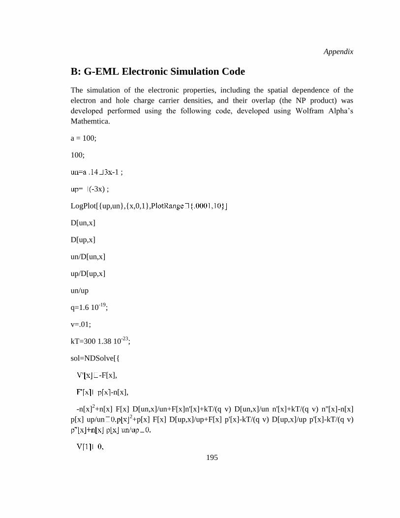
Appendix
195
B: G-EML Electronic Simulation Code
The simulation of the electronic properties, including the spatial dependence of the
electron and hole charge carrier densities, and their overlap (the NP product) was
developed performed using the following code, developed using Wolfram Alpha’s
Mathemtica.
a = 100;
100;
-1 ;
-3x) ;
LogPlot[{up,un},{x,0,1},P
D[un,x]
D[up,x]
un/D[un,x]
up/D[up,x]
un/up
q=1.6 10-19
;
v=.01;
kT=300 1.38 10-23
;
sol=NDSolve[{
-F[x],
-n[x],
-n[x]2+n[x] F[x] D[un,x]/un+F[x]n'[x]+kT/(q v) D[un,x]/un n'[x]+kT/(q v) n''[x]-n[x]
p[x] up/un2+p[x] F[x] D[up,x]/up+F[x] p'[x]-kT/(q v) D[up,x]/up p'[x]-kT/(q v)

Appendix
196
{p[x],n[x],F[x],V[x]},{x,0,1}]
Integrate[Evaluate[n[x]/.sol],{x,0,1}]
Integrate[Evaluate[p[x]/.sol],{x,0,1}]
Plot[{Evaluate[p[x]/.sol],Evaluate[n[x]/.sol],Evaluate[F[x]/.sol],Evaluate[V[x]/.sol]},{x,
0,1}]
Plot[{Evaluate[n[x] p[x]/.sol]},{x,0,1}]
{0.423302}
{0.422972}
Pplot = Partition[Flatten[Table[{i/100., Integrate[Evaluate[p[x] /. sol], {x, .01 i, .01 (i +
1)}]/.01}, {i, 0, 99}]], 2];
ListPlot[Pplot]
Plot[Evaluate[p[x] /. sol], {x, 0, 1}]
Plist = Flatten[Table[Integrate[Evaluate[p[x] /. sol], {x, .01 i, .01 (i + 1)}]/.01, {i, 0,
99}]];
Export["P(x).txt", Plist]
"P(x).txt"

Appendix
197
Nplot = Partition[Flatten[Table[{i/100., Integrate[Evaluate[n[x] /. sol], {x, .01 i, .01 (i +
1)}]/.01}, {i, 0, 99}]], 2];
ListPlot[Nplot]
Plot[Evaluate[n[x] /. sol], {x, 0, 1}]
Nlist = Flatten[Table[Integrate[Evaluate[n[x] /. sol], {x, .01 i, .01 (i + 1)}]/.01, {i, 0,
99}]];
Export["N(x).txt", Nlist]
ListPlot[Plist Nlist]
"P(x).txt"
"P(x).txt"
"N(x).txt"
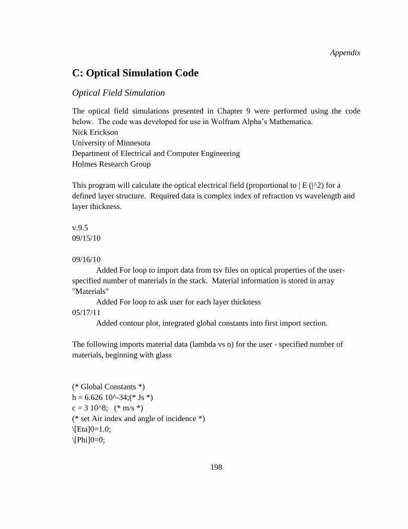
Appendix
198
C: Optical Simulation Code
Optical Field Simulation
The optical field simulations presented in Chapter 9 were performed using the code
below. The code was developed for use in Wolfram Alpha’s Mathematica.
Nick Erickson
University of Minnesota
Department of Electrical and Computer Engineering
Holmes Research Group
This program will calculate the optical electrical field (proportional to | E (|^2) for a
defined layer structure. Required data is complex index of refraction vs wavelength and
layer thickness.
v.9.5
09/15/10
09/16/10
Added For loop to import data from tsv files on optical properties of the user-
specified number of materials in the stack. Material information is stored in array
"Materials"
Added For loop to ask user for each layer thickness
05/17/11
Added contour plot, integrated global constants into first import section.
The following imports material data (lambda vs n) for the user - specified number of
materials, beginning with glass
(* Global Constants *)
h = 6.626 10^-34;(* Js *)
c = 3 10^8; (* m/s *)
(* set Air index and angle of incidence *)
\[Eta]0=1.0;
\[Phi]0=0;
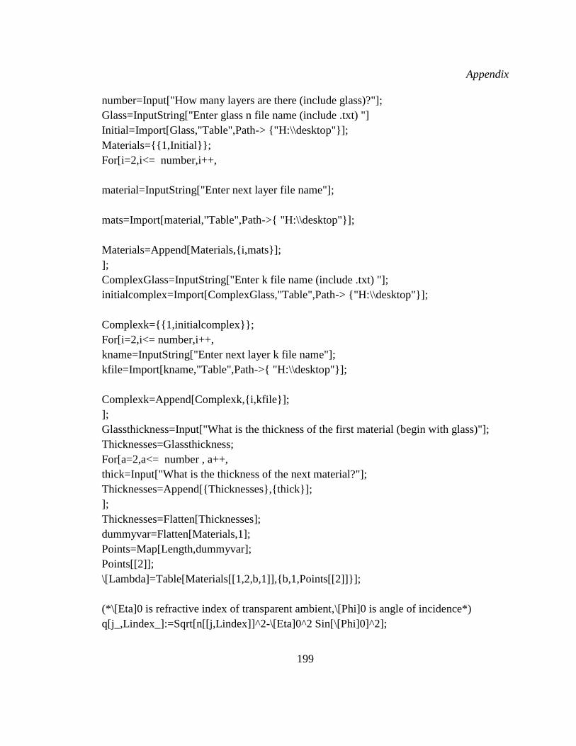
Appendix
199
number=Input["How many layers are there (include glass)?"];
Glass=InputString["Enter glass n file name (include .txt) "]
Initial=Import[Glass,"Table",Path-> {"H:\\desktop"}];
Materials={{1,Initial}};
For[i=2,i<= number,i++,
material=InputString["Enter next layer file name"];
mats=Import[material,"Table",Path->{ "H:\\desktop"}];
Materials=Append[Materials,{i,mats}];
];
ComplexGlass=InputString["Enter k file name (include .txt) "];
initialcomplex=Import[ComplexGlass,"Table",Path-> {"H:\\desktop"}];
Complexk={{1,initialcomplex}};
For[i=2,i<= number,i++,
kname=InputString["Enter next layer k file name"];
kfile=Import[kname,"Table",Path->{ "H:\\desktop"}];
Complexk=Append[Complexk,{i,kfile}];
];
Glassthickness=Input["What is the thickness of the first material (begin with glass)"];
Thicknesses=Glassthickness;
For[a=2,a<= number , a++,
thick=Input["What is the thickness of the next material?"];
Thicknesses=Append[{Thicknesses},{thick}];
];
Thicknesses=Flatten[Thicknesses];
dummyvar=Flatten[Materials,1];
Points=Map[Length,dummyvar];
Points[[2]];
\[Lambda]=Table[Materials[[1,2,b,1]],{b,1,Points[[2]]}];
(*\[Eta]0 is refractive index of transparent ambient,\[Phi]0 is angle of incidence*)
q[j_,Lindex_]:=Sqrt[n[[j,Lindex]]^2-\[Eta]0^2 Sin[\[Phi]0]^2];

Appendix
200
(*Fresnel complex reflection and transmission coefficients for s-polarized (E-field
perpendicular to plane of incidence,TE waves) at interface jk*)
rsjk[j_,Lindex_]:= (q[j,Lindex] - q[(j+1),Lindex])/(q[j,Lindex]+q[(j+1),Lindex])
tsjk[j_,Lindex_]:=(2 q[j,Lindex])/(q[j,Lindex]+q[(j+1),Lindex])
(*Fresnel complex reflection and transmission coefficients for p-polarized (E-Field
parallel to the plane of incidence,TM waves) at interface jk *)
rpjk[j_,Lindex_]:=(-n[[(j+1),Lindex]]^2 q[j,Lindex]+n[[j,Lindex]]^2
q[(j+1),Lindex])/(n[[(j+1),Lindex]]^2 q[(j),Lindex]+n[[j,Lindex]]^2 q[(j+1),Lindex])
tpjk[j_,Lindex_]:=(2 n[[j,Lindex]] n[[(j+1),Lindex]] q[j,Lindex])/(n[[(j+1),Lindex]]^2
q[j,Lindex]+n[[j,Lindex]]^2 q[(j+1),Lindex])
(*\[Xi][j] d[j] is the layer phase thickness corresponding to the phase change the wave
experiences as it traverses layer j:*)
\[Xi][j_,Lindex_]:=(2 \[Pi])/\[Lambda][[Lindex]] q[j,Lindex]
(*Interface matrix (matrix of refraction) for interface jk for p-polarized incident light:*)
Ipjk[j_,Lindex_]:=1/tpjk[j,Lindex] (1 rpjk[j,Lindex]
rpjk[j,Lindex] 1
)
(*Interface matrix (matrix of refraction) for interface jk for s-polarized incident light:*)
Isjk[j_,Lindex_]:=1/tsjk[j,Lindex] (1 rsjk[j,Lindex]
rsjk[j,Lindex] 1
)
(* Layer matrix (phase matrix) describing propagation through layer j *)
Lj[j_,Lindex_]:=(E^(-I \[Xi][j,Lindex] Thicknesses[[j]]) 0
0 E^(I \[Xi][j,Lindex] Thicknesses[[j]])
)
totalthick=Sum[Thicknesses[[i]],{i,1,Length[Thicknesses]}];
Length[\[Lambda]];
n={Table[(Materials[[1,2,b,2]]+I Complexk[[1,2,b,2]]),{b,1,Points[[2]]}]};
For[d=2,d<= number,d++,
n=Append[n,Table[Materials[[d,2,b,2]]+I Complexk[[d,2,b,2]],{b,1,Points[[2]]}]];

Appendix
201
];
(* This is an alternate thickness input which does not require inputing optical constants *)
Glassthickness = Input["What is the thickness of the first material (begin with glass)"];
Thicknesses = Glassthickness;
For[a = 2, a <= number , a++,
thick = Input["What is the thickness of the next material?"];
Thicknesses = Append[{Thicknesses}, {thick}];
];
Thicknesses = Flatten[Thicknesses];
totalthick = Sum[Thicknesses[[i]], {i, 1, Length[Thicknesses]}];
Length[\[Lambda]];
dummyvar = Flatten[Materials, 1];
Points = Map[Length, dummyvar];
Points[[2]];
Thicknesses = Flatten[Thicknesses]
totalthick = Sum[Thicknesses[[i]], {i, 1, Length[Thicknesses]}];
Length[\[Lambda]];
dummyvar = Flatten[Materials, 1];
Points = Map[Length, dummyvar];
Points[[2]];
{0, 0, 150, 10, 10, 10, 10, 10, 10, 10, 10, 10, 10, 100, 0}
For s-polarized light, calculate the system matrices, field and reflection
Timing[
Rglass=((1-n[[1]])/(1+n[[1]]))^2;
Tglass=(4 n[[1]])/(1+n[[1]])^2;
Rs={2};
Ts={3};
Ex={1};
For[l=1,l<= 451,l+=10,

Appendix
202
Ss=Isjk[1,l];
For[f=2, f<= (Length[Thicknesses]-1), f++,
Ss=Ss.Lj[f,l].Isjk[f,l];
];
Rs=Append[Rs,Re[Conjugate[Ss[[2,1]]/Ss[[1,1]]]*(Ss[[2,1]]/Ss[[1,1]])]];
Ts=Append[Ts,Re[Conjugate[1/Ss[[1,1]]]*(1/Ss[[1,1]])]];
For[m=2, m<= (Length[Thicknesses]), m++,
Sprime=Isjk[1,l];
For[p=3,p<= m,p++,
Sprime=Sprime.Lj[(p-1),l].Isjk[(p-1),l];
];
Sdoubleprime= (1 0
0 1
);
For[r=m,r<= (Length[Thicknesses]-1),r++,
Sdoubleprime=Sdoubleprime .Isjk[r,l]. Lj[(r+1),l];
];
For[x=1,x<= Thicknesses[[m]],x++,
Ex=Append[Ex,
Ts[[((l-1)/10+2)]]*((Sdoubleprime[[1,1]] E^(-I \[Xi][m,l] (Thicknesses[[m]]-
x))+Sdoubleprime[[2,1]] E^(I \[Xi][m,l] (Thicknesses[[m]]-
x)))/(Sprime[[1,1]]Sdoubleprime[[1,1]] E^(-I \[Xi][m,l] Thicknesses[[m]])+Sprime[[1,2]]
Sdoubleprime[[2,1]] E^(I \[Xi][m,l] Thicknesses[[m]])))
];
];
];

Appendix
203
];
Reflection=Table[(Rglass[[wave]]+Rs[[(wave-1)/10+2]]-2 Rglass[[wave]]*Rs[[(wave-
1)/10+2]])/(1-Rglass[[wave]]*Rs[[(wave-1)/10+2]]),{wave,1,450,10}];
Field={Table[Ex[[i]],{i,2,totalthick+1}]};
For[in=1,in<451/10,in++,
Field=Append[Field,Table[Ex[[i+in*totalthick+1]],{i,1,totalthick}]];
];
]
Thicknesses
{0, 0, 90, 30, 90, 30, 90, 30, 90, 30, 0}
Lambda=Input["What wavelength?"];
ListPlot[Re[Conjugate[Field[[((Lambda-350)/10)]]]*Field[[((Lambda-
350)/10)]]],DataRange->{0,totalthick},PlotRange-> All,AxesOrigin->{0,0},GridLines-
>{{Thicknesses[[2]],
Thicknesses[[3]]+Thicknesses[[2]],
Thicknesses[[2]]+Thicknesses[[3]]+Thicknesses[[4]],
Thicknesses[[2]]+Thicknesses[[3]]+Thicknesses[[4]]+Thicknesses[[5]],
Thicknesses[[2]]+Thicknesses[[3]]+Thicknesses[[4]]+Thicknesses[[5]]+Thicknesses[[6]]
,
Thicknesses[[2]]+Thicknesses[[3]]+Thicknesses[[4]]+Thicknesses[[5]]+Thicknesses[[6]]
+Thicknesses[[7]],
Thicknesses[[2]]+Thicknesses[[3]]+Thicknesses[[4]]+Thicknesses[[5]]+Thicknesses[[6]]
+Thicknesses[[7]]+Thicknesses[[8]],
Thicknesses[[2]]+Thicknesses[[3]]+Thicknesses[[4]]+Thicknesses[[5]]+Thicknesses[[6]]
+Thicknesses[[7]]+Thicknesses[[8]]+Thicknesses[[9]],
Thicknesses[[2]]+Thicknesses[[3]]+Thicknesses[[4]]+Thicknesses[[5]]+Thicknesses[[6]]
+Thicknesses[[7]]+Thicknesses[[8]]+Thicknesses[[9]]+Thicknesses[[10]],
Thicknesses[[2]]+Thicknesses[[3]]+Thicknesses[[4]]+Thicknesses[[5]]+Thicknesses[[6]]
+Thicknesses[[7]]+Thicknesses[[8]]+Thicknesses[[9]]+Thicknesses[[10]]+Thicknesses[[
11]],

Appendix
204
Thicknesses[[2]]+Thicknesses[[3]]+Thicknesses[[4]]+Thicknesses[[5]]+Thicknesses[[6]]
+Thicknesses[[7]]+Thicknesses[[8]]+Thicknesses[[9]]+Thicknesses[[10]]+Thicknesses[[
11]]+Thicknesses[[12]],
Thicknesses[[2]]+Thicknesses[[3]]+Thicknesses[[4]]+Thicknesses[[5]]+Thicknesses[[6]]
+Thicknesses[[7]]+Thicknesses[[8]]+Thicknesses[[9]]+Thicknesses[[10]]+Thicknesses[[
11]]+Thicknesses[[12]]+Thicknesses[[13]],
Thicknesses[[2]]+Thicknesses[[3]]+Thicknesses[[4]]+Thicknesses[[5]]+Thicknesses[[6]]
+Thicknesses[[7]]+Thicknesses[[8]]+Thicknesses[[9]]+Thicknesses[[10]]+Thicknesses[[
11]]+Thicknesses[[12]]+Thicknesses[[13]]+Thicknesses[[14]],
Thicknesses[[2]]+Thicknesses[[3]]+Thicknesses[[4]]+Thicknesses[[5]]+Thicknesses[[6]]
+Thicknesses[[7]]+Thicknesses[[8]]+Thicknesses[[9]]+Thicknesses[[10]]+Thicknesses[[
11]]+Thicknesses[[12]]+Thicknesses[[13]]+Thicknesses[[14]]+Thicknesses[[15]]},{}}]
ListPlot[Re[Reflection],AxesOrigin->{0,0},Filling->Axis]
Sorted = Table[Table[{j*10 + 340, i, Re[Conjugate[Field[[j, i]]]*Field[[j, i]]]}, {i, 1,
totalthick}], {j, 1, Length[Field]}];
ListPointPlot3D[Flatten[Sorted, 1], PlotStyle -> PointSize[Tiny], Axes -> True,
PlotRange -> All, AxesLabel -> {"Wavlength", "Thickness", "Field"}]
ListContourPlot[Flatten[Sorted, 1], Contours -> 20]
For p-polarized light, calculate the system matrices, field and reflection
p-polarized simulation has discontinuities at interfaces
Timing[
RPglass=((1-n[[1]])/(1+n[[1]]))^2;
TPglass=(4 n[[1]])/(1+n[[1]])^2;
Rp={2};
Tp={3};
ExP={1};
For[lp=1,lp<= 451,lp+=10,
Sp=Ipjk[1,lp];
For[fp=2, fp<= (Length[Thicknesses]-1), fp++,
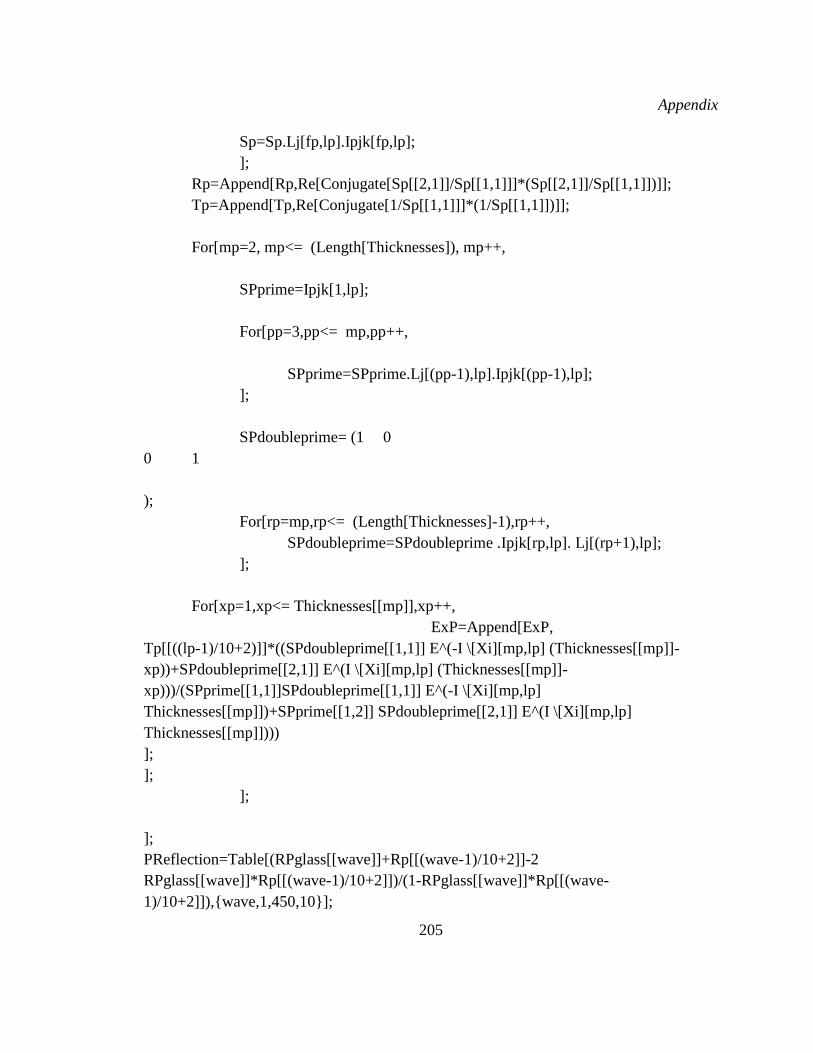
Appendix
205
Sp=Sp.Lj[fp,lp].Ipjk[fp,lp];
];
Rp=Append[Rp,Re[Conjugate[Sp[[2,1]]/Sp[[1,1]]]*(Sp[[2,1]]/Sp[[1,1]])]];
Tp=Append[Tp,Re[Conjugate[1/Sp[[1,1]]]*(1/Sp[[1,1]])]];
For[mp=2, mp<= (Length[Thicknesses]), mp++,
SPprime=Ipjk[1,lp];
For[pp=3,pp<= mp,pp++,
SPprime=SPprime.Lj[(pp-1),lp].Ipjk[(pp-1),lp];
];
SPdoubleprime= (1 0
0 1
);
For[rp=mp,rp<= (Length[Thicknesses]-1),rp++,
SPdoubleprime=SPdoubleprime .Ipjk[rp,lp]. Lj[(rp+1),lp];
];
For[xp=1,xp<= Thicknesses[[mp]],xp++,
ExP=Append[ExP,
Tp[[((lp-1)/10+2)]]*((SPdoubleprime[[1,1]] E^(-I \[Xi][mp,lp] (Thicknesses[[mp]]-
xp))+SPdoubleprime[[2,1]] E^(I \[Xi][mp,lp] (Thicknesses[[mp]]-
xp)))/(SPprime[[1,1]]SPdoubleprime[[1,1]] E^(-I \[Xi][mp,lp]
Thicknesses[[mp]])+SPprime[[1,2]] SPdoubleprime[[2,1]] E^(I \[Xi][mp,lp]
Thicknesses[[mp]])))
];
];
];
];
PReflection=Table[(RPglass[[wave]]+Rp[[(wave-1)/10+2]]-2
RPglass[[wave]]*Rp[[(wave-1)/10+2]])/(1-RPglass[[wave]]*Rp[[(wave-
1)/10+2]]),{wave,1,450,10}];

Appendix
206
FieldP={Table[ExP[[i]],{i,2,totalthick+1}]};
For[inp=1,inp<451/10,inp++,
FieldP=Append[FieldP,Table[ExP[[i+inp*totalthick+1]],{i,1,totalthick}]];
];
]
LambdaP=Input["What wavelength?"];
ListPlot[Re[Conjugate[FieldP[[((LambdaP-340)/10)]]]*FieldP[[((LambdaP-
340)/10)]]],DataRange->{0,totalthick},PlotRange-> All,AxesOrigin->{0,0},GridLines-
>{{Thicknesses[[2]],
Thicknesses[[3]]+Thicknesses[[2]],
+Thicknesses[[2]]+Thicknesses[[3]]+Thicknesses[[4]],
+Thicknesses[[2]]+Thicknesses[[3]]+Thicknesses[[4]]+Thicknesses[[5]]},{}}]
ListPlot[Re[PReflection],AxesOrigin->{0,0}]
SortedP = Table[Table[{j*10 + 340, i, Re[Conjugate[FieldP[[j, i]]]*FieldP[[j, i]]]}, {i, 1,
totalthick}], {j, 1, Length[FieldP]}];
ListPointPlot3D[Flatten[SortedP, 1], PlotStyle -> PointSize[Tiny], Axes -> True,
PlotRange -> All, AxesLabel -> {"Wavlength", "Thickness", "Field"}]

Appendix
207
Optical Emission and Outcoupling Simulation
The optical emission and outcoupling efficiency simulations presented in Chapter 10
were performed using the code below, developed in Wolfram Alpha’s Mathematica.
Glassthickness = Input["What is the thickness of the first material (begin with glass)"];
Thicknesses = Glassthickness;
For[a = 2, a <= number , a++,_thick = Input["What is the thickness of the next
material?"];_
Thicknesses = Append[{Thicknesses}, {thick}];
_];
Thicknesses = Flatten[Thicknesses];_
dummyvar = Flatten[Materials, 1];
Points = Map[Length, dummyvar];
Points[[2]];
totalthick = Sum[Thicknesses[[i]], {i, 1, Length[Thicknesses]}];
(* The following asks for the PL spectrum of the emitter (in 1nm steps from 350-800nm
*)_
plshape = InputString["Enter the normalized PL lineshape file name"];
PL = Import[plshape, "Table", Path -> { "H:\\desktop"}];
(* This initializes the n arry with glass n & k, the loop adds the other materials *)_
n = {Table[(Materials[[1, 2, b, 2]] + I Complexk[[1, 2, b, 2]]), {b, 1, Points[[2]]}]};_
For[d = 2, d <= number, d++,_n = Append[n, Table[Materials[[d, 2, b, 2]] + I
Complexk[[d, 2, b, 2]], {b, 1, Points[[2]]}]];
];
Thicknesses
{0, 0, 120, 10, 10, 10, 10, 10, 10, 10, 10, 10, 10, 100, 0}
This Subsection defines all system functions called in the loops
(* Global Constants *)
s angle of incidence*)
h = 6.626 10-34
;(* Js *)\.01
c = 3 108; (* m/s *)

Appendix
208
;
(*Fresnel complex reflection and transmission coefficients for s-polarized (E-field
perpendicular to plane of incidence,TE waves) at interface jk*)
rsjk -
(*Fresnel complex reflection and transmission coefficients for p-polarized (E-Field
parallel to the plane of incidence,TM waves) at interface jk *)
-n[[(j+1),Lindex]]2
2
2
2
+1),Lindex]] 2
2
experiences as it traverses layer j:*)
(*Interface matrix (matrix of refraction) for interface jk for p-polarized incident light:*)
})
(*Interface matrix (matrix of refraction) for interface jk for s-polarized incident light:*)
})
(* Layer matrix (phase matrix) describing propagation through layer j *)
-
})
The following imports material data (lambda vs n) for the user-specified number of
materials, beginning with glass
number = Input["How many layers are there (include glass)?"];
Glass = InputString["Enter glass n file name (include .txt) "];_
Initial = Import[Glass, "Table", Path -> {"H:\\desktop"}];
n j, Lindex2
0 Sin180
2
Appendix
209
Materials = {{1, Initial}};
For[i = 2, i <= number, i++,_
material = InputString["Enter next layer file name"];_
mats = Import[material, "Table", Path -> { "H:\\desktop"}];_
Materials = Append[Materials, {i, mats}];
];
ComplexGlass = InputString["Enter k file name (include .txt) "];
initialcomplex = Import[ComplexGlass, "Table", Path -> {"H:\\desktop"}];
Complexk = {{1, initialcomplex}};
For[i = 2, i <= number, i++,_
kname = InputString["Enter next layer k file name"];
kfile = Import[kname, "Table", Path -> { "H:\\desktop"}];
Complexk = Append[Complexk, {i, kfile}];
];
Glassthickness = Input["What is the thickness of the first material (begin with glass)"];
Thicknesses = Glassthickness;
For[a = 2, a <= number , a++,_thick = Input["What is the thickness of the next
material?"];_
Thicknesses = Append[{Thicknesses}, {thick}];
_];
Thicknesses = Flatten[Thicknesses];_
dummyvar = Flatten[Materials, 1];
Points = Map[Length, dummyvar];
Points[[2]];
totalthick = Sum[Thicknesses[[i]], {i, 1, Length[Thicknesses]}];
(* The following asks for the PL spectrum of the emitter (in 1nm steps from 350-800nm
*)_
plshape = InputString["Enter the normalized PL lineshape file name"];

Appendix
210
PL = Import[plshape, "Table", Path -> { "H:\\desktop"}];
(* This initializes the n arry with glass n & k, the loop adds the other materials *)_
n = {Table[(Materials[[1, 2, b, 2]] + I Complexk[[1, 2, b, 2]]), {b, 1, Points[[2]]}]};_
For[d = 2, d <= number, d++,_n = Append[n, Table[Materials[[d, 2, b, 2]] + I
Complexk[[d, 2, b, 2]], {b, 1, Points[[2]]}]];
];
(* This is an alternate thickness input which does not require inputing optical constants *)
For s-polarized light, calculate the system matrices and field
*PL[[Lindex,2]];
AShm[Lind - *PL[[Lindex,2]];
Timing[
SSL = {1};
SSR = {1};
For[Lindex = 1, Lindex < 451, Lindex++,
SSSL = {{1, 1}, {1, 1}};
SSSR = {{1, 1}, {1, 1}};
-
SSSL = Append[SSSL,
SSSR = Append[SSSR,
];
SSL = Append[SSL, SSSL];
SSR = Append[SSR, SSSR];
3
16
3
16

Appendix
211
];
]
{390.782505, Null}
Timing[
E0Svm = {1};
For[j = 3, j < 182, j++,
E0Svm2 = {1};
For[l = 2, l < 452, l++, E0Svm2 = Append[E0Svm2, (SSR[[l, j, 2, 1]]*ASvp[l - 1, j - 2]
- SSR[[l, j, 1, 1]]*ASvm[l - 1, j - 2])/(SSL[[l, j, 2, 2]]*SSR[[l, j, 1, 1]] - SSR[[l, j, 2,
1]]*SSL[[l, j, 1, 2]])];
];
E0Svm = Append[E0Svm, E0Svm2];
];
E0Shm = {1};
For[j = 3, j < 182, j++,
E0Shm2 = {1};
For[l = 2, l < 452, l++,
E0Shm2 = Append[E0Shm2, (SSR[[l, j, 2, 1]]*AShp[l - 1, j - 2] - SSR[[l, j, 1,
1]]*AShm[l - 1, j - 2])/(SSL[[l, j, 2, 2]]*SSR[[l, j, 1, 1]] - SSR[[l, j, 2, 1]]*SSL[[l, j, 1,
2]])];
];
E0Shm = Append[E0Shm, E0Shm2];
];
]
{15.350498, Null}
Timing[
Field = E0S = Table[Table[.5*Conjugate[E0Svm[[i, j]]]*E0Svm[[i, j]] +
.5*Conjugate[E0Shm[[i, j]]]*E0Shm[[i, j]], {i, 2, 180}], {j, 2, 451}];
]
{0.514803, Null}
Field[[180, 90]]
AShp[180, 90]
0.0271067 + 0. I
0.208721
SumField = Table[Sum[Field[[i, l]], {i, 1, 450}], {l, 1, 179}];

Appendix
212
SumFieldL = Table[Sum[Field[[i, l]], {l, 1, 179}], {i, 1, 450}];
ListPlot[Re[SumField]]
ListPlot[Re[SumField], PlotRange -> All]
ListPlot[Re[SumFieldL]]
ListPlot[Re[SumFieldL], PlotRange -> All]
For p-polarized light, calculate the system matrices and field
*PL[[Lindex,2]];
*PL[[Lindex,2]];
- *PL[[Lindex,2]];
- *PL[[Lindex,2]];
Timing[
PSL = {1};
PSR = {1};
For[Lindex = 1, Lindex < 451, Lindex++,
PSSL = {{1, 1}, {1, 1}};
PSSR = {{1, 1}, {1, 1}};
-
PSSL = Append[PSSL,
PSSR = Append[PSSR,
];
PSL = Append[PSL, PSSL];
PSR = Append[PSR, PSSR];
];
]
{421.655103, Null}
3
8Sin 89
180
2
3
16Cos 89
180
2
3
8Sin 89
180
2
3
16Cos 89
180
2

Appendix
213
Timing[
E0Pvm = {1};
For[j = 3, j < 182, j++,
E0Pvm2 = {1};
For[l = 2, l < 452, l++, E0Pvm2 = Append[E0Pvm2, (PSR[[l, j, 2, 1]]*APvp[l - 1, j - 2]
- PSR[[l, j, 1, 1]]*APvm[l - 1, j - 2])/(PSL[[l, j, 2, 2]]*PSR[[l, j, 1, 1]] - PSR[[l, j, 2,
1]]*PSL[[l, j, 1, 2]])];
];
E0Pvm = Append[E0Pvm, E0Pvm2];
];
E0Phm = {1};
For[j = 3, j < 182, j++,
E0Phm2 = {1};
For[l = 2, l < 452, l++,
E0Phm2 = Append[E0Phm2, (PSR[[l, j, 2, 1]]*APhp[l - 1, j - 2] - PSR[[l, j, 1,
1]]*APhm[l - 1, j - 2])/(PSL[[l, j, 2, 2]]*PSR[[l, j, 1, 1]] - PSR[[l, j, 2, 1]]*PSL[[l, j, 1,
2]])];
];
E0Phm = Append[E0Phm, E0Phm2];
];
]
{61.979197, Null}
Timing[
FieldP = E0P = Table[Table[.5*Conjugate[E0Pvm[[i, j]]]*E0Pvm[[i, j]] +
.5*Conjugate[E0Phm[[i, j]]]*E0Phm[[i, j]], {i, 2, 180}], {j, 2, 451}];
SumFieldP = Table[Sum[FieldP[[i, l]], {i, 1, 450}], {l, 1, 179}];
SumFieldLP = Table[Sum[FieldP[[i, l]], {l, 1, 179}], {i, 1, 450}];
]
{10.873270, Null}
ListPlot[Re[SumFieldP]]
ListPlot[Re[SumFieldP], PlotRange -> All]
ListPlot[Re[SumFieldLP]]
ListPlot[Re[SumFieldLP], PlotRange -> All]
This Section puts the S and P simulations together
(* Total field versus wavelength *)

Appendix
214
TotalFieldAngle = Table[.5*SumFieldP[[i]] + .5*SumField[[i]], {i, 1, 179}];
(* Total Field verus Angle *)
TotalFieldWave = Table[.5*SumFieldL[[i]] + .5*SumFieldLP[[i]], {i, 1, 450}];
ListPlot[Re[TotalFieldWave]]
ListPlot[Re[TotalFieldWave], PlotRange -> All]
ListPlot[Re[TotalFieldAngle]]
ListPlot[Re[TotalFieldAngle], PlotRange -> All];
Sum[Re[TotalFieldAngle[[i]]], {i, 1, 179}]
Sum[Re[TotalFieldWave][[i]], {i, 1, 450}]
288.597
288.597
Angle=Table[{i*0.0174533,
Re[TotalFieldAngle[[i]]]},{i,1,179}];
ListPolarPlot[{Angle,1.7*Table[Cos[(90-
Output = Table[Angle[[i, 2]], {i, 1, 179}];
WaveOutput = Table[Re[TotalFieldWave[[i]]], {i, 1, 450}];
Angle2=Table[{i*0.0174533,
3 Cos[((i-
2)/(Mean[Abs[n[[5]]]]
3-
2
Mean[Abs[n[[5]]]] Sin[((i-2)]},{i,1,179}];
a2=Max/@Transpose[Angle2];
AnglePlot2=Table[{i*0.0174533,Angle2[[i,2]]/a2[[2]]},{i,1,179}];
ListPolarPlot[{Table[Cos[(90-
Export["angle.txt", Output]
Export["wave.txt", WaveOutput]
"angle.txt"
"wave.txt"
CorAngle=Table[
3 Cos[((i-
2)/(Mean[Abs[n[[5]]]]
3-
2
Mean[Abs[n[[5]]]] Sin[((i-2)],{i,1,179}];
Export["CorAngle.txt", CorAngle]
"CorAngle.txt"
ListPlot[WaveOutput]
indexedPL = Table[PL[[i, 2]], {i, 1, 451}];
ListPlot[{indexedPL, Re[TotalFieldWave]/Re[Max[TotalFieldWave]]}, PlotRange ->
All]
SourceP=Table[Sum[Re[APhp[l,a]2+APvp[l,a]
2],{a,0,360}],{l,1,451}];

Appendix
215
Sum[SourceP[[i]],{i,1,451}]
SourceS=Table[Sum[Re[AShp[l,a]2+ASvp[l,a]
2],{a,0,360}],{l,1,451}];
Sum[SourceS[[i]],{i,1,451}]
1535.28
1022.58
Sum[SumFieldLP[[i]], {i, 1, 450}]
Sum[SumFieldL[[i]], {i, 1, 450}]
Outcoupling = Re[(Sum[SumFieldLP[[i]], {i, 1, 450}] + Sum[SumFieldL[[i]], {i,
450}])/(Sum[SourceP[[i]], {i, 1, 451}] + Sum[SourceS[[i]], {i, 1, 451}])]
403.162 + 0. I
174.032 + 0. I
0.225656

Appendix
216
D: Copyright notices Applied Physics Letters:
AIP PUBLISHING LLC LICENSE
TERMS AND CONDITIONS
Nov 12, 2013
All payments must be made in full to CCC. For payment instructions, please see
information listed at the bottom of this form.
License Number 3266671423036
Order Date Nov 12, 2013
Publisher AIP Publishing LLC
Publication Applied Physics Letters
Article Title Highly efficient, single-layer organic light-emitting devices based on a
graded-composition emissive layer
Author Nicholas C. Erickson, Russell J. Holmes
Online Publication Date Aug 27, 2010
Volume number 97
Issue number 8
Type of Use Thesis/Dissertation
Requestor type Author (original article)
Format Print and electronic
Portion Excerpt (> 800 words)
Will you be translating? No
Title of your thesis / dissertation
On the Design and Properties of Organic Light Emitting Devices
Expected completion date Jan 2014
Estimated size (number of pages) 180
Total 0.00 USD
Terms and Conditions
AIP Publishing LLC -- Terms and Conditions: Permissions Uses
AIP Publishing LLC ("AIPP"") hereby grants to you the non-exclusive right and license
to use and/or distribute the Material according to the use specified in your order, on a
one-time basis, for the specified term, with a maximum distribution equal to the number
that you have ordered. Any links or other content accompanying the Material are not the
subject of this license.
Journal of Applied Physics

Appendix
217
AIP PUBLISHING LLC LICENSE
TERMS AND CONDITIONS
Nov 12, 2013
All payments must be made in full to CCC. For payment instructions, please see
information listed at the bottom of this form.
License Number 3266680185258
Order Date Nov 12, 2013
Publisher AIP Publishing LLC
Publication Journal of Applied Physics
Article Title Relating charge transport and performance in single-layer graded
composition organic light-emitting devices
Author Nicholas C. Erickson, Russell J. Holmes
Online Publication Date Oct 31, 2011
Volume number 110
Issue number 8
Type of Use Thesis/Dissertation
Requestor type Author (original article)
Format Print and electronic
Portion Excerpt (> 800 words)
Will you be translating? No
Title of your thesis / dissertation
On the Design and Properties of Organic Light Emitting Devices
Expected completion date Jan 2014
Estimated size (number of pages) 180
Total 0.00 USD
Terms and Conditions
AIP Publishing LLC -- Terms and Conditions: Permissions Uses AIP Publishing LLC
("AIPP"") hereby grants to you the non-exclusive right and license to use and/or
distribute the Material according to the use specified in your order, on a one-time basis,
for the specified term, with a maximum distribution equal to the number that you have
ordered. Any links or other content accompanying the Material are not the subject of this
license.
Advanced Functional Materials:
JOHN WILEY AND SONS LICENSE
TERMS AND CONDITIONS

Appendix
218
Nov 12, 2013
This is a License Agreement between Nicholas C Erickson ("You") and John Wiley and
Sons
("John Wiley and Sons") provided by Copyright Clearance Center ("CCC"). The license
consists of your order details, the terms and conditions provided by John Wiley and Sons,
and the payment terms and conditions. All payments must be made in full to CCC. For
payment instructions, please see information listed at the bottom of this form.
License Number 3266680649617
License date Nov 12, 2013
Licensed content publisher John Wiley and Sons
Licensed content publication Advanced Functional Materials
Licensed content title High-Transconductance Organic Thin-Film Electrochemical
Transistors for Driving Low-Voltage Red-Green-Blue Active Matrix Organic Light-
Emitting Devices
Licensed copyright line Copyright © 2012 WILEY-VCH Verlag GmbH & Co. KGaA,
Weinheim
Licensed content author Daniele Braga, Nicholas C. Erickson, Michael J. Renn, Russell J.
Holmes, C. Daniel Frisbie
Licensed content date Feb 14, 2012
Start page 1623
End page 1631
Type of use Dissertation/Thesis
Requestor type Author of this Wiley article
Format Print and electronic
Portion Full article
Will you be translating? No
Total 0.00 USD
Terms and Conditions
TERMS AND CONDITIONS
This copyrighted material is owned by or exclusively licensed to John Wiley & Sons, Inc.
or one of its group companies (each a "Wiley Company") or a society for whom a Wiley
Company has exclusive publishing rights in relation to a particular journal (collectively
"WILEY"). By clicking "accept" in connection with completing this licensing
transaction, you agree that the following terms and conditions apply to this transaction
(along with the billing and payment terms and conditions established by the Copyright
Clearance Center/ Inc., ("CCC's Billing and Payment terms and conditions"), at the time

Appendix
219
that you opened your Rights Link account (these are available at any time at
http://myaccount.copyright.com). Rights link Printable License
https://s100.copyright.com/App/PrintableLicenseFrame.jsp?publisherID=... 1 of 6
11/12/2013 2:44 PM
JOHN WILEY AND SONS LICENSE
TERMS AND CONDITIONS
Nov 12, 2013
This is a License Agreement between Nicholas C Erickson ("You") and John Wiley and
Sons ("John Wiley and Sons") provided by Copyright Clearance Center ("CCC"). The
license consists of your order details, the terms and conditions provided by John Wiley
and Sons, and the payment terms and conditions.
All payments must be made in full to CCC. For payment instructions, please see
information listed at the bottom of this form.
License Number 3266671022250
License date Nov 12, 2013
Licensed content publisher John Wiley and Sons
Licensed content publication Advanced Functional Materials
Licensed content title Investigating the Role of Emissive Layer Architecture on the
Exciton
Recombination Zone in Organic Light-Emitting Devices
Licensed copyright line Copyright © 2013 WILEY-VCH Verlag GmbH & Co. KGaA,
Weinheim
Licensed content author Nicholas C. Erickson, Russell J. Holmes
Licensed content date Apr 19, 2013
Start page 5190
End page 5198
Type of use Dissertation/Thesis
Requestor type Author of this Wiley article
Format Print and electronic
Portion Full article
Will you be translating? No
Total 0.00 USD
TERMS AND CONDITIONS
This copyrighted material is owned by or exclusively licensed to John Wiley & Sons, Inc.
or one of its group companies (each a "Wiley Company") or a society for whom a Wiley
Company has exclusive publishing rights in relation to a particular journal (collectively

Appendix
220
"WILEY"). By clicking "accept" in connection with completing this licensing
transaction, you agree that the following terms and conditions apply to this transaction
(along with the
billing and payment terms and conditions established by the Copyright Clearance Center
Inc., ("CCC's Billing and Payment terms and conditions"), at the time that you opened
your Rights Link account (these are available at any time at
http://myaccount.copyright.com).