open access - project presentation
TRANSCRIPT

IEEE TRANSACTIONS ON MICROWAVE THEORY AND TECHNIQUES 1
Abstract—This paper presents holistic design of a novel 4-waydifferential power-combining transformer for use in mm-wavepower-amplifier (PA). The combiner with an inner radius of 25um exhibits a record low insertion loss of 1.25 dB at 83.5 GHz. Itis designed to simultaneously act as a balanced-to-unbalancedconverter, removing the need for additional BALUNs typicallyrequired in differential circuits. A complete circuit comprised ofa power splitter, two-stage differential cascode PA array, a powercombiner as well as input and output matching elements wasdesigned and realized in SiGe technology with fT/fmax 170/250GHz. Measured small-signal gain of at least 16.8 dB was obtainedfrom 76.4 GHz to 85.3 GHz with a peak 19.5 dB at 83 GHz. Theprototype delivered 12.5 dBm output referred 1 dB compressionpoint and 14 dBm saturated output power when operated from a3.2 V DC supply voltage at 78 GHz.
Index Terms—Cascode, differential circuit, E-band, hetero-junction bipolar transistor (HBT), integrated circuit (IC), mm-wave, power amplifier, power combiner, silicon germanium(SiGe), transformer.
I. INTRODUCTION
OST wireless radio communications nowadays operate atfrequencies below 10 GHz where bandwidth is priceless
due to already congested frequency spectrum. As demand forultra high-speed data transfer unprecedentedly increases, largebandwidth is required. One of the trivial solutions to this issueis through a migration to mm-wave frequency regime. Toname a few, the unlicensed 60 GHz frequency band allocatedfor indoor applications and the newly licensed yet inexpensive71-76 GHz and 81-86 GHz E-band intended for backhaulapplications provide a generous bandwidth of several GHzworldwide. Despite this bandwidth advantage, the path lossincurred at mm-wave frequencies is substantially high. As anillustration, the loss due to oxygen absorption reaches its peak15 dB/km at around 60 GHz. Consequently, to enabling long-range distance data transmission, high effective isotropic
Manuscript received Jul. 25, 2012. This work was supported by FP7 MarieCurie IAPP “GigaRadio”.
M. Thian was with the ECIT Institute, Queen’s University of Belfast, U.K.He is on a secondment to Infineon Technologies AG, Villach A9500, Austria(e-mail: [email protected]).
M. Tiebout and F. Dielacher are with Infineon Technologies AG, VillachA9500, Austria.
N.B. Buchanan and V.F. Fusco are with the ECIT Institute, Queen’sUniversity of Belfast, U.K.
radiated power (EIRP) is required. Given the gain of theantenna array, the EIRP would in turn dictate the output powerlevel of the power amplifier (PA).
Meanwhile, breakthroughs in nanotechnology and opticshave enabled the production of high-performance high-speedtransistors in low-cost highly-integrated silicon technology. Asa direct result, the III-V based technologies such as GaAs andInP that have in the past decade been dominating the marketfor mm-wave wireless products are being greatly challenged.For instance, the 60/77/79 GHz PAs reported in [1]-[7] and[8]-[14] were triumphantly implemented in CMOS and SiGeprocesses, respectively.
Recently, there have been significant research efforts onmm-wave silicon PA that attempt to achieve output power atleast 20 dBm derived from the EIRP specification for long-range radios. This high power level cannot realistically beachieved by merely relying on the capability of the largestdevice that even the most advanced silicon IC process cannowadays offer. This stems from the inevitable natural trade-off that as the fT of the transistors increases the breakdownvoltage BVCEO decreases, limiting the signal swing and hencereducing the output power. In addition, thermal dissipationdue to typically poor efficiency of the mm-wave PAseventually reduces the output power further down. In SiGeprocess, an increase in temperature from, say, 25O C to 85O Ctypically results in 2-3 dB power reduction.
In order to relax the design specifications for the PAs, giventhe challenges described above, power-combining techniquesutilizing passive structures can be adopted. Traditionally,output power from the PAs can be combined in phase usingthe Wilkinson structure [11] illustrated in Fig. 1(a). TheWilkinson combiner is formed by two λ/4 transmission lines(TLs) with characteristic impedance ZT = Z0√2 (Z0 is thesystem characteristic impedance) and a ballast resistor of 2Z0
that provides an excellent isolation between the input ports. Incases where three or more PAs (n ≥ 3) are combined, the Wilkinson structure is no longer planar since the ballastresistors will cross over one another. Besides, the value of ZT
will increase. For example, for n = 4, ZT will be 2Z0. For a50 Ω system, this means 100 Ω. In SiGe process [15], the maximum realizable ZT is about 70 Ω, associated with the smallest metal width allowed by the technology. To getaround this issue, Z0 can be set to 35 Ω rather than 50 Ω.
A 76-84 GHz SiGe Power Amplifier ArrayEmploying Low-Loss 4-Way Differential
Combining Transformer
Mury Thian, Marc Tiebout, Member, IEEE, Neil B. Buchanan, Vincent F. Fusco, Fellow, IEEE, andFranz Dielacher, Senior Member, IEEE
M

IEEE TRANSACTIONS ON MICROWAVE THEORY AND TECHNIQUES 2
(a) (b) (c)
Fig. 1. Power-combining techniques: (a) Wilkinson, (b) λ/4 transmission-line, and (c) transformer
Fig. 2. Schematic of the proposed 4-way differential combining PA
TABLE ICIRCUIT COMPONENT VALUES
However, in this scenario a matching element to transform35 Ω back to 50 Ω is required, adding more complexity and losses. Alternatively, multiple 2-way Wilkinson structures tocombine, say, 4 or 8 PAs can be used but the interconnectionscan be daunting and any mismatches introduced by theseinterconnections will degrade the overall performance.
As in the Wilkinson structure, the high-efficiency Class-EPA reported in [16]-[17] employs λ/4 TLs to combine powerbut without the ballast resistor, Fig. 1(b). This leads to, asexpected, a rather poor isolation but can be tolerated so longas the leakage energy injected from one port to another doesnot substantially affect the circuit’s operation.
Another power-combining strategy proposed in [1]-[4], [10]
and [12] is based upon transformers, Fig. 1(c). While the λ/4TL combiners are bulky and lossy, particularly if implementedin low-resistivity silicon substrate, the transformer-basedcombiners offer very compact geometry. To give anillustration, the inner diameter of the power-combiningtransformer designed at 80 GHz centre frequency is only 50µm in contrast to 465 µm electrical length of the λ/4 TL at thesame frequency. Importantly, these transformers can alsosimultaneously provide an impedance transformation (thehigher the number of input ports, the higher the impedancetransformation ratio) and balanced-to-unbalanced conversionroles, thus dispensing the need for additional matchingelements as well as for BALUNs typically required indifferential circuits.
To date, there are only a few publications reporting on mm-wave transformers with combining capability of more thantwo single-ended paths. For example, the transformersdemonstrated in [2]-[4] and [10] realized in CMOS and SiGe,respectively, are able to combine four single-ended pathsefficiently. This paper will discuss the design of a novelcompact 8-way power-combining transformer and itsimplementation in SiGe technology. The loss of the combineris only 1.25 dB at 83.5 GHz centre frequency of 81-86 GHz E-band. For practical validations, a complete circuit comprised
IEEE TRANSACTIONS ON MICROWAVE THEORY AND TECHNIQUES 3
of a power splitter, two-stage differential cascode PA array, apower combiner as well as input and output (I/O) matchingnetworks is built. The circuit schematic is depicted in Fig. 2and the circuit component values are given in Table I.
II. TECHNOLOGY
Active and passive circuits presented in this paper aredesigned and implemented using Infineon B7HF200 SiGeprocess [15]. The HBT transistors are fabricated with adouble-polysilicon self-aligned emitter base configurationwith a selectively grown SiGe:C base. High-speed (HS) ratherthan ultra-high-speed (UHS) transistors are chosen since theyoffer higher BVCEO and BVCES values, 1.7 V and 6.5 V,respectively. The peak of fT 170 GHz and the peak of fmax 250GHz occur at a collector current density 5 mA/μm2. Theseparameters are obtained from the measurements of transistorswith emitter mask size 0.35 × 2.8 µm2 or effective emitter size(0.35-0.17) × (2.8-0.17) µm2.
Four copper metal layers (M1–M4) are available forinterconnections as well as for implementation of passiveelements. The microstrip lines are realized using the top metalM4 and M2 as the ground plane. The width of the groundplane is set three times larger than the width of the signal line.The smallest available pad measures 68 × 68 μm2 and has aparasitic capacitance CPAD 25 fF. Metal-insulator-metal (MIM)capacitors as well as TaN and polysilicon resistors are alsoprovided in B7HF200 process. The key features of thetechnology and the cross section of the metal layer stack arepresented in Fig. 3.
(a) (b)
Fig. 3. (a) Core features of the Infineon B7HF200 technology and (b) crosssection of the metal layer stack
III. ACTIVE CIRCUITS: POWER AMPLIFIER AND DRIVER
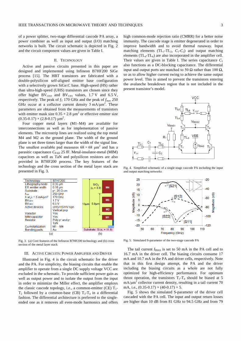
Illustrated in Fig. 4 is the circuit schematic for the driverand the PA. For simplicity, the biasing circuits that enable theamplifier to operate from a single DC supply voltage VCC areexcluded in the schematic. To provide sufficient power gain aswell as output power and to isolate the output from the inputin order to minimize the Miller effect, the amplifier employsthe classic cascode topology, i.e., a common-emitter (CE) T1-T2 followed by a common-base (CB) T3-T4 in a differentialfashion. The differential architecture is preferred to the single-ended one as it removes all even-mode harmonics and offers
high common-mode rejection ratio (CMRR) for a better noiseimmunity. The cascode stage is emitter degenerated in order toimprove bandwidth and to avoid thermal runaway. Inputmatching elements (TL1-TL2, C1-C2) and output matchingelements (TL4-TL6) are also incorporated in the amplifier cell.Their values are given in Table I. The series capacitance C1
also functions as a DC-blocking capacitance. The differentialinput and output ports are matched to 50 Ω rather than 100 Ω, so as to allow higher current swing to achieve the same outputpower level. This is aimed to prevent the transistors enteringthe avalanche breakdown region that is not included in thepresent transistor’s model.
Fig. 4. Simplified schematic of a single-stage cascode PA including the inputand output matching networks
Fig. 5. Simulated S-parameter of the two-stage cascode PA
The tail current IBIAS is set to 50 mA in the PA cell and to16.7 mA in the driver cell. The biasing circuits consume 17mA and 10.7 mA in the PA and driver cells, respectively. Notethat in this first design attempt, the PA and the driverincluding the biasing circuits as a whole are not fullyoptimized for high-efficiency performance. For optimumthrust operation, the transistors T1-T4 should be biased at 5mA/μm2 collector current density, resulting in a tail current 70mA, i.e., (0.35-0.17) × (40-0.17) × 5.
Fig. 5 shows the simulated S-parameter of the driver cellcascaded with the PA cell. The input and output return lossesare higher than 10 dB from 81 GHz to 94.5 GHz and from 79

IEEE TRANSACTIONS ON MICROWAVE THEORY AND TECHNIQUES 4
GHz to 90 GHz, respectively. The small-signal gain of at least18 dB is obtained within 66.7-88.6 GHz bandwidth and itreaches the peak 23 dB at 80.5 GHz. The isolation is higherthan 60 dB across the simulated frequencies.
IV. PASSIVE STRUCTURES: POWER-SPLITTING/COMBINING
TRANSFORMER AND ROUTING LINE
The design of a power-combining transformer involves anumber of iterative optimization procedures with the primaryaim to obtain the lowest insertion loss possible. There are twokey factors that contribute to the loss of the combiner, namely,magnetic coupling factor (k) and port mismatch.
Fig. 6. Proposed 4-way differential combining transformer (4WDCT)
Fig. 7. Simulated insertion loss and output return loss of the 4WDCT
TABLE IICOMPARISON WITH STATE-OF-THE-ART MM-WAVE POWER COMBINERS
The 3-D view of the proposed 8-way single-ended or 4-waydifferential combining transformer (4WDCT) is presented inFig. 6. The vertical broadside-coupled structure is adoptedhere since it offers higher k than the horizontal edge-coupled
counterpart. Two input transformers are realized on M2 andM4 while M3 is used for the output transformer. Each inputtransformer has two pairs of differentially excited ports whilethe output transformer has only one pair. If one of these outputports is grounded, the combiner will simultaneously exhibit asa BALUN. RF currents coming out from the PA array willcirculate in the input transformers producing a set of magneticflux. This magnetic flux is exposed to the output transformer,generating an RF current that will flow to the load. Fourdifferential ports in the input transformers are arrangedperpendicular to one another so as to prevent energy beingtransferred between them. Since the number of turns of theoutput transformer is twice that of the input transformer, theimpedance seen at each input port should ideally be onequarter of the load impedance. This means that the output PAconnected to the input of the power-combining transformercan be matched to lower impedances, relaxing the voltagestress on the transistors.
Design parameters that are typically optimized include thetransformer radius and the trace width. The transformer radiusis a strong function of the input susceptance and therefore itcritically contributes to the port mismatch. In addition, shuntcapacitance CY, Fig. 2, is added to the input transformer portsto further improve the port mismatch. The transformer radiusalso determines the self-resonance frequency (SRF), i.e., thesmaller the radius, the lower the inductance, the higher theSRF. It is important to make sure that the SRF is sufficientlyfar above the operating frequency. Meanwhile, the trace widthdetermines the unloaded Q-factor of the metal winding self-inductance, i.e., the wider the trace, the lower the parasiticelectrical series resistance (ESR), the higher the Q. Ideally, thetrace width is set to the maximum metal width allowed by thetechnology but this may require larger chip area. Further, incases where the combining transformer is also intended toprovide DC access, i.e., to bias the PAs, it is vital that the tracewidth complies with the maximum current density of the metalwinding. The inner diameter of the octagon-shaped 4WDCT inFig. 6 is 50 μm and the trace width is 5 μm.
Due to the symmetry of the structure, the input impedancesseen at port 1 and 3 are identical. The same applies to theimpedances at port 2 and 4. On the other hand, since theelectrical properties of M2 and M4 are not equivalent, it isexpected that ZIN1 = ZIN3 ≠ ZIN2 = ZIN4. The S-parametersof the 4WDCT simulated in SONNET are plotted in Fig. 7.Here, the differential ports of the input transformers areterminated with the shunt capacitance 2CY in parallel with50 Ω resistance. One of the ports of the output transformer is grounded whereas another one is terminated with CPAD inparallel with 50 Ω resistance. The output return loss |S55| is higher than 10 dB from 70 GHz to 92 GHz. As predicted, it isobserved that |S51| = |S53| ≠ |S52| = |S54| across thefrequency band of interest. At 83.5 GHz, |S51| = |S53| = -6.9dB, |S52| = -7.7 dB, and |S54| = -7.5 dB. This means that if 0dBm RF power is injected to port 5, the combined powerappear at port 1-4 will be 10×log(10-0.69 + 10-0.69 + 10-0.77 + 10-
0.75) = -1.25 dBm, implying a loss of 1.25 dB or equivalent to75% efficiency. This result is also confirmed by the harmonic-

IEEE TRANSACTIONS ON MICROWAVE THEORY AND TECHNIQUES 5
balance (HB) simulation in ADS and SPECTRE. The insertionloss of the proposed 4WDCT is compared to state-of-the-artmm-wave power combiners in Table II.
Up to this point, the designs of the driver and PA cells aswell as the 4WDCT have been discussed independently. Oneof the remaining challenges is associated with the technique toconnect the output of the PAs to the input of the 4WDCT.Used as routing lines are the series microstrip lines, TLX andTLY, which together with the shunt capacitance CX form alow-pass filter. This is depicted in Fig. 8 and their values aregiven in Table I. These routing lines have to be designedaccurately with attentive care as any presence of amplitudeand/or phase imbalance among the eight paths would cause thesignals not being combined constructively and therefore woulddeteriorate the overall circuit performance. Fig. 9 shows thesimulated return loss and insertion loss of the routing-lineelement. Broadband input and output matching are achieved.Insertion loss is lower than 0.8 dB from 70.5 GHz to 85 GHz.
Fig. 8. Routing lines with capacitive compensators
Fig. 9. Simulated return loss and insertion loss of the routing-line element
Fig. 10. Simulated S-parameter of the two-stage cascode PA with routing-lineelements connected at its input and output
Simulated S-parameters of the two-stage cascode PA withrouting-line element attached to both its input and output areplotted in Fig. 10. Compared with Fig. 5, the I/O matching andthe reverse transmission are not substantially altered althoughit appears from the |S11| plot that the routing-line elementsintroduce a new higher-frequency pole at around 115 GHz.The small-signal gain of at least 18 dB is obtained within 68-87 GHz bandwidth and it reaches the peak 21.4 dB at 80.5GHz. This peak is 1.6 dB lower than that in Fig. 5 due to 0.8dB loss introduced by each routing-line element.
Simulated power gain versus output power of the two-stagecascode PA with and without the routing-line elements arepresented in Fig. 11. The 1.6 dB reduction in small-signal gainagrees well with the S-parameter results. The routing-lineelement at the output of the PA reduces the output referred1 dB compression point, OP-1dB, to 12 dBm from 12.9 dBm.
Fig. 11. Simulated power gain versus output power of the two-stage cascodePA with and without the routing-line elements
V. MEASUREMENT RESULTS
The chip microphotograph of the complete PA is shown inFig. 12. It occupies 675 × 1264 μm2 active die area. EachPA/driver cell including the biasing circuits measures 130 ×260 μm2. The amplifier was characterized through on-chipmeasurements with 100 µm pitch GSG probes used to probeboth input and output ports.
Fig. 12. Chip microphotograph of the complete PA including the 4WDCT
IEEE TRANSACTIONS ON MICROWAVE THEORY AND TECHNIQUES 6
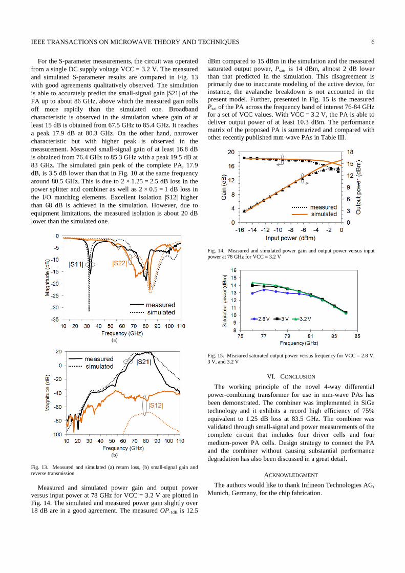
For the S-parameter measurements, the circuit was operatedfrom a single DC supply voltage VCC = 3.2 V. The measuredand simulated S-parameter results are compared in Fig. 13with good agreements qualitatively observed. The simulationis able to accurately predict the small-signal gain |S21| of thePA up to about 86 GHz, above which the measured gain rollsoff more rapidly than the simulated one. Broadbandcharacteristic is observed in the simulation where gain of atleast 15 dB is obtained from 67.5 GHz to 85.4 GHz. It reachesa peak 17.9 dB at 80.3 GHz. On the other hand, narrowercharacteristic but with higher peak is observed in themeasurement. Measured small-signal gain of at least 16.8 dBis obtained from 76.4 GHz to 85.3 GHz with a peak 19.5 dB at83 GHz. The simulated gain peak of the complete PA, 17.9dB, is 3.5 dB lower than that in Fig. 10 at the same frequencyaround 80.5 GHz. This is due to 2 × 1.25 = 2.5 dB loss in thepower splitter and combiner as well as 2 × 0.5 = 1 dB loss inthe I/O matching elements. Excellent isolation |S12| higherthan 68 dB is achieved in the simulation. However, due toequipment limitations, the measured isolation is about 20 dBlower than the simulated one.
(a)
(b)
Fig. 13. Measured and simulated (a) return loss, (b) small-signal gain andreverse transmission
Measured and simulated power gain and output powerversus input power at 78 GHz for VCC = 3.2 V are plotted inFig. 14. The simulated and measured power gain slightly over18 dB are in a good agreement. The measured OP-1dB is 12.5
dBm compared to 15 dBm in the simulation and the measuredsaturated output power, Psat, is 14 dBm, almost 2 dB lowerthan that predicted in the simulation. This disagreement isprimarily due to inaccurate modeling of the active device, forinstance, the avalanche breakdown is not accounted in thepresent model. Further, presented in Fig. 15 is the measuredPsat of the PA across the frequency band of interest 76-84 GHzfor a set of VCC values. With VCC = 3.2 V, the PA is able todeliver output power of at least 10.3 dBm. The performancematrix of the proposed PA is summarized and compared withother recently published mm-wave PAs in Table III.
Fig. 14. Measured and simulated power gain and output power versus inputpower at 78 GHz for VCC = 3.2 V
Fig. 15. Measured saturated output power versus frequency for VCC = 2.8 V,3 V, and 3.2 V
VI. CONCLUSION
The working principle of the novel 4-way differentialpower-combining transformer for use in mm-wave PAs hasbeen demonstrated. The combiner was implemented in SiGetechnology and it exhibits a record high efficiency of 75%equivalent to 1.25 dB loss at 83.5 GHz. The combiner wasvalidated through small-signal and power measurements of thecomplete circuit that includes four driver cells and fourmedium-power PA cells. Design strategy to connect the PAand the combiner without causing substantial performancedegradation has also been discussed in a great detail.
ACKNOWLEDGMENT
The authors would like to thank Infineon Technologies AG,Munich, Germany, for the chip fabrication.

IEEE TRANSACTIONS ON MICROWAVE THEORY AND TECHNIQUES 7
TABLE IIICOMPARISON WITH RECENTLY PUBLISHED MM-WAVE PAS
REFERENCES
[1] D. Chowdhury, P. Reynaert, and A.M. Niknejad, “A 60 GHz 1 V +12.3dBm transformer-coupled wideband PA in 90 nm CMOS,” IEEEInternational Solid-State Circuits Conference (ISSCC) Dig. Tech.Papers, San Francisco, Feb. 2008, pp. 560-561.
[2] J. Chen and A.M. Niknejad, “A compact 1 V 18.6 dBm 60 GHz poweramplifier in 65 nm CMOS,” IEEE International Solid-State CircuitsConference (ISSCC) Dig. Tech. Papers, San Francisco, Feb. 2011, pp.432-433.
[3] D. Zhao, S. Kulkarni, and P. Reynaert, “A 60 GHz outphasingtransmitter in 40 nm CMOS with 15.6 dBm output power,” IEEEInternational Solid-State Circuits Conference (ISSCC) Dig. Tech.Papers, San Francisco, Feb. 2012, pp. 170-172.
[4] K.-Y. Wang, T.-Y. Chang, and C.-K. Wang, “A 1 V 19.3 dBm 79 GHzpower amplifier in 65 nm CMOS,” IEEE International Solid-StateCircuits Conference (ISSCC) Dig. Tech. Papers, San Francisco, Feb.2012, pp. 260-261.
[5] T.-Y. Chang, C.-S. Wang, and C.-K. Wang, “A 77 GHz power amplifierusing transformer-based power combiner in 90 nm CMOS,” IEEECustom Integrated Circuits Conference (CICC), San Jose, CA, Sep2010, pp. 1-4.
[6] Y.A. Li, M.H. Hung, S.J. Huang, and J. Lee, “A fully integrated 77 GHzFMCW radar system in 65 nm CMOS,” IEEE International Solid-StateCircuits Conference (ISSCC) Dig. Tech. Papers, San Francisco, Feb.2010, pp. 216-217.
[7] J. Lin, K. To, D. Hammock, B. Knappenberger, M. Majerus, and W.Huang, “Power amplifier for 77-GHz automotive radar in 90-nm LPCMOS technology,” IEEE Microw. Wireless Compon. Lett., vol. 20, no.5, pp. 292-294, May. 2010.
[8] U.R. Pfeiffer, S.K. Reynolds, and B.A. Floyd, “A 77 GHz SiGe poweramplifier for potential applications in automotive radar systems,” inIEEE Radio Frequency Integrated Circuits (RFIC) Symp. Dig., FortWorth, Texas, Jun. 2004, pp. 91-94.
[9] E. Afshari, H. Bhat, X. Li, and A. Hajimiri, “Electrical funnel: Abroadband signal combining method,” IEEE International Solid-StateCircuits Conference (ISSCC) Dig. Tech. Papers, San Francisco, Feb.2006, pp. 751-760.
[10] Y. Zhao, J.R. Long, M. Spirito, and A.B. Akhnoukh, “A +18 dBm, 79-87.5 GHz bandwidth power amplifier in 0.13 µm SiGe-BiCMOS,” IEEEBipolar/BiCMOS Circuits and Technology Meeting (BCTM), Atlanta,Georgia, Oct. 2011, pp. 17-20.
[11] L. Wang, J. Borngraeber, W. Winkler, and C. Scheytt, “A 77 GHzMMIC power amplifier driver for automotive radar,” IET InternationalConference on Radar Systems, Edinburgh, U.K., Oct. 2007, pp. 1-4.
[12] V. Giammello, E. Ragonese, and G. Palmisano, “A transformer-couplingcurrent-reuse SiGe HBT power amplifier for 77-GHz automotive radar,”IEEE Trans. Microw. Theory Tech., vol. 60, no. 6, pp. 1676-1683, Jun.2012.
[13] V. Giammello, E. Ragonese, and G. Palmisano, “Transmitter chipset for24/77-GHz automotive radar sensors,” in IEEE Radio FrequencyIntegrated Circuits (RFIC) Symp. Dig., Anaheim, CA, May. 2010, pp.75-78.
[14] N. Demirel, E. Kerherve, D. Pache, and R. Plana, “Design techniquesand considerations for mm-wave SiGe power amplifiers,” in IEEEInternational Microwave and Optoelectronics Conference (IMOC),Belem, Brazil, Nov. 2009, pp. 37-41.
[15] J. Böck, H. Schäfer, K. Aufinger, R. Stengl, S. Boguth, R. Schreiter, M.Rest, H. Knapp, M. Wurzer, W. Perndl, T. Böttner, and T. F. Meister,“SiGe bipolar technology for automotive radar applications,” in Proc.IEEE Bipolar/BiCMOS Circuits Technology Meeting, Montreal, QC,Canada, Sep. 2004, pp. 84-87.
[16] M. Thian and V. Fusco, “Power combining techniques into unbalancedloads for Class-E and Inverse Class-E amplifiers,” IET Microw.Antennas Propag., vol. 2, no. 6, pp. 529-537, Sep 2008.
[17] M. Thian, V. Fusco, and P. Gardner, “Power-combining Class-Eamplifier with finite choke,” IEEE Trans. Circuits Syst I., vol. 58, no. 3,pp. 451-457, Mar. 2011.
Mury Thian obtained the B.Sc. degree from AtmaJaya Catholic University, Jakarta, Indonesia, theM.Sc. degree from Delft University of Technology(TU Delft), the Netherlands, and the Ph.D. degreefrom the Queen’s University of Belfast, U.K., all inelectronics engineering.
He was with Philips (now NXP)Semiconductors, Nijmegen, the Netherlands, as anRFIC designer and with the University ofBirmingham, U.K., as a postdoctoral research
fellow. From 2009 to 2011, he worked at the ECIT Institute, Queen’sUniversity Belfast designing mm-wave transceivers. Since 2011, he has beenwith Infineon Technologies AG, Villach, Austria, as a Marie Curie fellow. Hiscurrent research interests include analogue and mixed-signal circuits,RFIC/MMIC design, wireless transceivers for high-speed datacommunication, and efficiency enhancement and linearization techniques forpower amplifiers.
Dr. Thian has authored over 30 journal and conference papers and is theco-author of a book chapter. He was invited to co-chair a session during the2010 Asia Pacific Microwave Conference (APMC) in Yokohama, Japan. Hewas the 2008 finalist of the British Association for the Advancement ofScience.
Marc Tiebout (S’90-M’93) was born in Asse,Belgium, in 1969. He received the M.Sc. degree inelectrical and mechanical engineering in 1992 fromthe Katholieke Universiteit Leuven, Belgium, and thePh.D. degree in electrical engineering from theTechnical University of Berlin, Germany, in 2004.
In 1993, he joined Siemens AG, CorporateResearch and Development, Microelectronics inMunich, Germany, designing analog integratedcircuits in CMOS and BiCMOS technologies. In
1997, he started the design of radio frequency devices and building blocks insub-µm CMOS technologies. From 1999 to 2005, he was with InfineonTechnologies AG, Munich, Germany, where he worked on RF CMOS circuitsand transceivers for cellular wireless communication products and conductedhighest frequency RF CMOS research for 17 and 24 GHz applications. Since2006, he is with Infineon Technologies, Villach, Austria where his workincludes Wimedia-UWB CMOS SoC development (system architect) andhighest frequency phased-array radar applications.
Dr. Tiebout has authored and co-authored more than 60 IEEE publicationsand holds more than 10 patents. His interest goes into RFIC design in SiliconTechnologies.

IEEE TRANSACTIONS ON MICROWAVE THEORY AND TECHNIQUES 8
Neil B. Buchanan received a B.Eng. Hons degreefrom the Queens University of Belfast in 1993. InJuly 2000, he graduated with a Ph.D. entitled"Phase Locked Millimetre Wave HEMTOscillators" from the Queens University of Belfastand is currently employed as a Senior Engineerwithin the High Frequency Electronics Group atthat university.
His research interests include self-steered (retro-directive) antennas, super regenerative detectors,
injection-locked oscillators, and mm-wave MMIC design. He has publishedover 40 papers in refereed journals and conferences and has providedconsultancy to a number of companies. He has acted as technical manager fora number of research/industrial projects and has refereed IEE/IEEE journalsand conferences.
Vincent Fusco (S’82-M’82-SM’96-F’04) obtainedhis Bachelor’s degree in Electrical and ElectronicEngineering (First Class Honours) and his Ph.D. inMicrowave Electronics from the Queen’s Universityof Belfast. Since 1995, he has held a personal chairin High Frequency Electronic Engineering.
His research interests include nonlinearmicrowave circuit design, and active and passiveantenna techniques. The main focus for this researchis in the area of wireless communications. At present
he is technical director of the High Frequency Laboratories at ECIT(www.ecit.qub.ac.uk), where he is also director of the International Centre forResearch for System on Chip and Advanced MicroWireless Integration(SoCaM).
Prof. Fusco has published numerous scientific papers in major journals andin referred international conferences, and is the author of two text books. Heholds several patents and has contributed invited chapters to books in the fieldof active antenna design and EM field computation. He is a Fellow of theRoyal Academy of Engineering, a Fellow of the Institution of Engineering andTechnology (IET), a Fellow of the Institute of Electrical and ElectronicEngineers (IEEE), and of the Royal Irish Academy. In 1986, he was awardeda British Telecommunications Fellowship and in 1997 he was awarded the NIEngineering Federation Trophy for outstanding industrially relevant research.
Franz Dielacher (S’-M’-SM’) received his M.S.and Ph.D. degrees in electrical engineering from theGraz University of Technology, Austria, in 1981 and1990, respectively. His doctoral research wasdirected towards the modeling, simulation anddesign of oversampled analog-to-digital converters.
From 1981 until 1999, he worked for SiemensSemiconductor Group in circuit development andsystem integration for wireline and wirelesscommunications. Since 1999, he is with Infineon
Technologies in various positions in circuits and systems for communicationslike DSL, high-speed transceivers, wireless infrastructure, wirelessconnectivity and telecom standardization. Currently he is a Senior PrincipalEngineer and Chief Scientist in the RF-Power Group.
Dr. Dielacher is a senior member of the IEEE. His internationalinvolvement includes ISSCC TPC member from 2001 to 2011, ISSCCwireline subcommittee chair, ESSCIRC TPC member, ESSCIRC technicalprogram committee chair in 2001, ESSCIRC steering board member since2005, IEEE JSSC guest editor in 2002, SSCS AdCOM member since 2011and conference chair for AACD (Advances in Analog Circuit Design) in1995. In 2000, he and his team received the Austrian Innovations Award andseveral of his product innovations are described in the book-series “ProductInnovations in Austria”. He is the author and co-author of many scientificpapers and several book chapters and holds many patents with several morepending. He has contributed to numerous conference and workshoppresentations and is a lecturer at advanced engineering courses.