operator manual osd480 series rf/catv…osd.com.au/wp-content/uploads/2013/01/10101907.pdf ·...
TRANSCRIPT

OPERATOR MANUAL
OSD480 SERIES
RF/CATV/MATV TRANSMISSION
SYSTEMS
OSD481A/OSD483A CATV/MATV MODEM
PAIR


OPTICAL SYSTEMS DESIGN
DOC ID: 10101907
OSD480 OPERATOR MANUAL
PAGE 3
INDEX 1
1 TECHNICAL SUMMARY ........................................................................................................ 4
1.1 BRIEF DESCRIPTION ............................................................................................................ 4
1.1.1 OVERVIEW............................................................................................................................................. 4
1.1.2 APPLICATIONS...................................................................................................................................... 4
1.1.3 FEATURES AND BENEFITS ................................................................................................................. 4
1.2 OSD480 CONFIGURATION ................................................................................................... 5
1.2.1 OSD481A/483A UNIT ............................................................................................................................. 5
1.2.2 TYPICAL CONFIGURATION ............................................................................................................... 5
1.3 TECHNICAL SPECIFICATIONS ........................................................................................... 6
1.4 OSD480 FRONT AND REAR PANELS .................................................................................. 7
2 INSTALLATION AND OPERATION ..................................................................................... 8
2.1 INTRODUCTION .................................................................................................................... 8
2.2 INSTALLATION ..................................................................................................................... 8
2.2.1 WARNING AND PRECAUTIONS ......................................................................................................... 8
2.2.2 OSD480 DRAWINGS AND DIMENSIONS ........................................................................................... 9
2.2.3 POWER SUPPLY CONNECTIONS ..................................................................................................... 10
2.2.4 DB9 PIN ASSIGNMENTS .................................................................................................................... 10
2.2.5 LED INDICATORS ............................................................................................................................... 11
2.2.6 CONTROLS ........................................................................................................................................... 12
2.2.7 RF INPUT POWER LIMIT ................................................................................................................... 12
2.2.8 RECEIVER OPTICAL INPUT LIMIT .................................................................................................. 13
2.3 SYSTEM SETTINGS RECOMMENDATIONS .................................................................... 13
2.4 SYSTEM ADJUSTMENTS ................................................................................................... 13
3 MAINTENANCE...................................................................................................................... 14
3.1 INTRODUCTION .................................................................................................................. 14
3.2 EXTERNAL INSPECTION ................................................................................................... 14
3.3 ROUTINE MAINTENANCE ................................................................................................. 14
4 WARRANTY ............................................................................................................................ 15
4.1 WARRANTY PERIOD .......................................................................................................... 15
4.2 REPAIRS ................................................................................................................................ 15
4.2.1 WARRANTY REPAIRS........................................................................................................................ 15
4.2.2 OUT-OF-WARRANTY REPAIRS ........................................................................................................ 15
4.2.3 SITE REPAIRS ...................................................................................................................................... 15
4.2.4 EXCLUSIONS ....................................................................................................................................... 15
FIGURE 1: OSD481A/483A UNIT ......................................................................................................... 5
FIGURE 2: OSD480 TYPICAL CONFIGURATION ............................................................................. 5
FIGURE 3: OSD480 FRONT AND REAR PANELS ............................................................................. 7
FIGURE 4: OSD480 MOUNTING DIMENSIONS ................................................................................ 9
FIGURE 5: OSD480 POWER SUPPLY CONNECTIONS ................................................................... 10
FIGURE 6: OSD480 LED INDICATORS ............................................................................................. 11
FIGURE 7: OSD481 CONTROLS ......................................................................................................... 12
TABLE 1: TECHNICAL SPECIFICATIONS ......................................................................................... 6
TABLE 2: OSD481A DB9 PIN ASSIGNMENTS ................................................................................. 10
TABLE 3: OSD483A DB9 PIN ASSIGNMENTS ................................................................................. 10
TABLE 4: LED FUNCTION ................................................................................................................. 11
TABLE 5: OSD481A TRANSMITTER ATTENUATOR SETTINGS ................................................. 12

OPTICAL SYSTEMS DESIGN
DOC ID: 10101907
OSD480 OPERATOR MANUAL
PAGE 4
1 TECHNICAL SUMMARY
1.1 BRIEF DESCRIPTION
1.1.1 OVERVIEW
The OSD481A/483A combination provides optical transmission of a composite AM-VSB CATV
spectrum of television and FM radio carriers within the 30 to 860MHz frequency range. The optical
signal is transmitted over single mode optical fiber cable that may be up to 20km in length, depending
on the number of channels and grade of laser used.
The OSD481A is available with three grades of laser, which permit the following levels of
performance: G1 : 20 channels, > +2dBm optical output power G2 : 40 channels, > +8dBm optical output power G3 : 60 channels, >+10.5dBm optical output power
The system is intended for the reticulation of television signals in environments such as hotels, resorts,
hospitals and other large sites.
The OSD481A optical transmitter accepts a combined RF spectrum with a level of 90dBuV per
channel and outputs a linearly modulated optical signal via a single mode fiber. The unit is normally
supplied for point to point links, however it can be fitted with a 1:2, 1:4 or 1:8 optical splitter which
permits a point to multi-point network.
The OSD483A receiver accepts the incoming optical signal, converts it to an electrical signal and
outputs this signal to an external network.
Both OSD481A and OSD483A are supplied as stand-alone 120/240VAC powered 1RU high 19” rack
mountable enclosures.
1.1.2 APPLICATIONS
CATV networking MATV networks for resorts, hospitals Secure reticulation of television and
data in defense and government sites
and campuses
Distance learning UHF/VHF radio links Very wideband multiple channel data
transmission
1.1.3 FEATURES AND BENEFITS
Available to support 60 channel
networks Operates over from 5 to at least 50km
of singlemode cable depending on the
laser employed in the OSD481A
transmitter modem Can support star networks with up to
16 remote nodes
Optionally available in a form
suitable to RF over fiber signal
distribution Very cost effective – you pay only for
what you really need

OPTICAL SYSTEMS DESIGN
DOC ID: 10101907
OSD480 OPERATOR MANUAL
PAGE 5
1.2 OSD480 CONFIGURATION
Note that the manual will refer to the OSD480 when referring to both the OSD481 and OSD483
1.2.1 OSD481A/483A UNIT
FIGURE 1: OSD481A/483A UNIT
1.2.2 TYPICAL CONFIGURATION
Figure 2 below indicates a possible set-up for an OSD480 system.
Point-to-Point Link :OSD481A
OSD4831 fiber
60ch CATV or
other 30-860MHz RF signal
60ch CATV or
other 30-860MHz RF signal
fiber
OSD481A
60ch CATV or
other 30-860MHz RF signal
fiber 1
fiber 2
fiber 3
fiber N
OSD483
OSD483
OSD483
OSD483
60ch CATV or
other 30-860MHz
RF signal
60ch CATV or
other 30-860MHz
RF signal
60ch CATV or
other 30-860MHz
RF signal
60ch CATV or
other 30-860MHz
RF signal
Station 1
Station 2
Station 3
Station N
1 Point to N Points Link :
1xN
Splitter
FIGURE 2: OSD480 TYPICAL CONFIGURATION
OPTICAL SYSTEMS DESIGN
DOC ID: 10101907
OSD480 OPERATOR MANUAL
PAGE 6
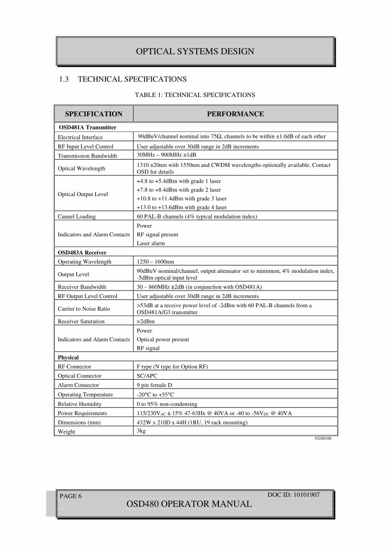
1.3 TECHNICAL SPECIFICATIONS
TABLE 1: TECHNICAL SPECIFICATIONS
SPECIFICATION PERFORMANCE
OSD481A Transmitter
Electrical Interface 90dBuV/channel nominal into 75Ω, channels to be within ±1.0dB of each other
RF Input Level Control User adjustable over 30dB range in 2dB increments
Transmission Bandwidth 30MHz – 900MHz ±1dB
Optical Wavelength 1310 ±20nm with 1550nm and CWDM wavelengths optionally available. Contact
OSD for details
Optical Output Level
+4.8 to +5.4dBm with grade 1 laser
+7.8 to +8.4dBm with grade 2 laser
+10.8 to +11.4dBm with grade 3 laser
+13.0 to +13.6dBm with grade 4 laser
Cannel Loading 60 PAL-B channels (4% typical modulation index)
Indicators and Alarm Contacts
Power
RF signal present
Laser alarm
OSD483A Receiver
Operating Wavelength 1250 – 1600nm
Output Level 90dBuV nominal/channel, output attenuator set to minimum, 4% modulation index,
-5dBm optical input level
Receiver Bandwidth 30 – 860MHz ±2dB (in conjunction with OSD481A)
RF Output Level Control User adjustable over 30dB range in 2dB increments
Carrier to Noise Ratio >53dB at a receive power level of -2dBm with 60 PAL-B channels from a
OSD481A/G3 transmitter
Receiver Saturation >2dBm
Indicators and Alarm Contacts
Power
Optical power present
RF signal
Physical
RF Connector F type (N type for Option RF)
Optical Connector SC/APC
Alarm Connector 9 pin female D
Operating Temperature -20°C to +55°C
Relative Humidity 0 to 95% non-condensing
Power Requirements 115/230VAC ± 15% 47-63Hx @ 40VA or -40 to -56VDC @ 40VA
Dimensions (mm) 432W x 210D x 44H (1RU, 19 rack mounting)
Weight 3kg
10248106

OPTICAL SYSTEMS DESIGN
DOC ID: 10101907
OSD480 OPERATOR MANUAL
PAGE 7
1.4 OSD480 FRONT AND REAR PANELS
OSD481A
There are three LED indicators and two Laser bias sockets on the front panel of the OSD481A
The rear panel consists of the DB9 Alarm connector, RF input connector, optical output level adjust
panel and power/fuse/switch IEC inlet.
OSD483A
There are two LED indicators and two Rx Optical Power sockets.
The rear panel consists of the DB9 Alarm connector, RF output connector, optical input level adjust
panel and power/fuse/switch IEC inlet.
FIGURE 3: OSD480 FRONT AND REAR PANELS

OPTICAL SYSTEMS DESIGN
DOC ID: 10101907
OSD480 OPERATOR MANUAL
PAGE 8
2 INSTALLATION AND OPERATION
2.1 INTRODUCTION
This section outlines the methods required to install and operate the OSD480 successfully. It should be
studied carefully if damage to the equipment or poor results are to be avoided.
This equipment has been fully tested prior to dispatch and is ready for immediate operation. However it
is advisable to check for external transportation damage before operation. If damage is evident, return
the unit with the packaging to your supplier immediately.
2.2 INSTALLATION
2.2.1 WARNING AND PRECAUTIONS ELECTROMAGNETIC COMPATIBILITY
WARNING: This is a Class A product. In a domestic environment this product may cause radio
interference in which case the user may be required to take adequate measures.
OPTICAL OUTPUT OPERATION
WARNING: Laser Safety: Class 1M Laser Product per IEC/EN 60825-1:20011 standard.
Class 1M
The OSD481A is a Class 1M laser product.
PRECAUTIONS
All service personnel should be provided training as to the hazards of direct viewing of laser
radiation and of the precautionary measures during servicing of equipment Areas where laser products are installed should be restricted in access to trained service
personnel only and appropriate warning signs posted in the work area. All laser apertures should be covered by protective covers when not connected to optical
fibers. Never leave outputs uncovered. Laser equipment should be positioned above or below eye level where possible. Apertures
should be positioned away from personnel. Protective eyewear should be worn in the vicinity of laser equipment.

OPTICAL SYSTEMS DESIGN
DOC ID: 10101907
OSD480 OPERATOR MANUAL
PAGE 9
2.2.2 OSD480 DRAWINGS AND DIMENSIONS
The OSD4840 standalone module is designed to be mounted on a 19” rack or an even bench surface.
FIGURE 4: OSD480 MOUNTING DIMENSIONS
432mm
44mm
210mm
OPTICAL SYSTEMS DESIGN
DOC ID: 10101907
OSD480 OPERATOR MANUAL
PAGE 10
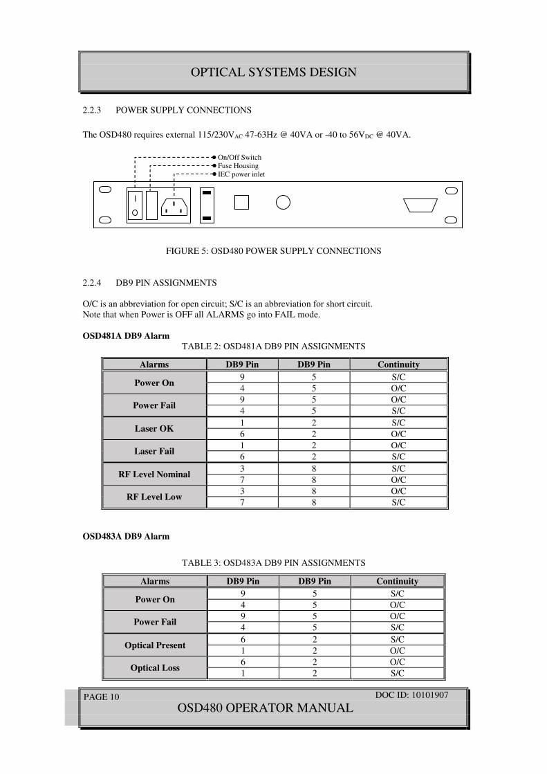
2.2.3 POWER SUPPLY CONNECTIONS
The OSD480 requires external 115/230VAC 47-63Hz @ 40VA or -40 to 56VDC @ 40VA.
FIGURE 5: OSD480 POWER SUPPLY CONNECTIONS
2.2.4 DB9 PIN ASSIGNMENTS
O/C is an abbreviation for open circuit; S/C is an abbreviation for short circuit.
Note that when Power is OFF all ALARMS go into FAIL mode.
OSD481A DB9 Alarm
TABLE 2: OSD481A DB9 PIN ASSIGNMENTS
Alarms DB9 Pin DB9 Pin Continuity
Power On 9 5 S/C
4 5 O/C
Power Fail 9 5 O/C
4 5 S/C
Laser OK 1 2 S/C
6 2 O/C
Laser Fail 1 2 O/C
6 2 S/C
RF Level Nominal 3 8 S/C
7 8 O/C
RF Level Low 3 8 O/C
7 8 S/C
OSD483A DB9 Alarm
TABLE 3: OSD483A DB9 PIN ASSIGNMENTS
Alarms DB9 Pin DB9 Pin Continuity
Power On 9 5 S/C
4 5 O/C
Power Fail 9 5 O/C
4 5 S/C
Optical Present 6 2 S/C
1 2 O/C
Optical Loss 6 2 O/C
1 2 S/C
On/Off Switch
Fuse Housing
IEC power inlet
OPTICAL SYSTEMS DESIGN
DOC ID: 10101907
OSD480 OPERATOR MANUAL
PAGE 11
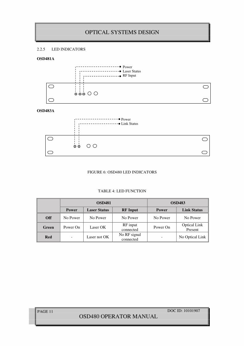
2.2.5 LED INDICATORS
OSD481A
OSD483A
FIGURE 6: OSD480 LED INDICATORS
TABLE 4: LED FUNCTION
OSD481 OSD483
Power Laser Status RF Input Power Link Status
Off No Power No Power No Power No Power No Power
Green Power On Laser OK RF input
connected Power On
Optical Link
Present
Red - Laser not OK No RF signal
connected - No Optical Link
Power
Laser Status
RF Input
Power
Link Status

OPTICAL SYSTEMS DESIGN
DOC ID: 10101907
OSD480 OPERATOR MANUAL
PAGE 12
2.2.6 CONTROLS
OSD481
The RF input level to the transmitter may be adjusted by means of an attenuation switch located on the
OSD481A rear panel. There are two push buttons marked [+] and [-] to increment or decrement
attenuation level located on the rear of the unit. The level is changed in 2dB increments and there are
sixteen discrete attenuation levels: from 0 to F (hexadecimal).
It is important to set the attenuator so that the laser is working with optimum modulation.
Recommended attenuator settings for a 4mW laser are shown in Table 5.
FIGURE 7: OSD481 CONTROLS
Table 5: OSD481A Transmitter Attenuator Settings
Number of Carriers RF Level at input port (dBuV) Attenuator
control
1 95 2
79 95 C
OSD483
There is one user adjustment available on the OSD483A receiver located on the rear of the unit. It is a
broadband, low distortion gain adjustment, which can be used to set the system (OSD481A/483A) gain
to other than unity.
External amplifiers/attenuators may be necessary to achieve the desired levels required for each
particular installation.
The key requirement is to keep optical power levels as high as possible short of causing visible
distortion products.
2.2.7 RF INPUT POWER LIMIT
Precautions have to be taken not to overdrive the OSD481A RF input with excessive signal level.
Laser damage may occur as a result of excessive signal power being applied to the input.
The maximum RF power applied to the RF input port of the OSD481A must not exceed +118dBuV
when the attenuator is set to 0.
For this reason it is recommended to set the OSD481A RF attenuator control to position [F] (maximum
attenuation) before connecting RF signals to the OSD481A input. The attenuator control is located at
the rear panel of the unit and consists of two push buttons marked [+] and [-] to increment or decrement
attenuation level. The attenuation level is changed in 2dB increments and there are sixteen discrete
attenuation levels: from 0 to F (hexadecimal).
Level Adjust
OPTICAL SYSTEMS DESIGN
DOC ID: 10101907
OSD480 OPERATOR MANUAL
PAGE 13
2.2.8 RECEIVER OPTICAL INPUT LIMIT
OSD483A uses a photodiode that is designed to work at optical powers of less than +2dBm. It is
necessary to ensure that optical power going into OSD483A input is less than +2dBm, or damage
to the unit may occur. The OSD481A transmitted optical power can be as high as +11dBm. In
situations where optical path attenuation is not high enough, a fixed optical attenuator must be used to
reduce optical power at the OSD483A receiver input to less than +2dBm.
2.3 SYSTEM SETTINGS RECOMMENDATIONS
For best results, please note the following:
ALL AM-VSB Fiber Optic Transmission Systems operate best if:
1. Input television carriers are within ±1dB of each other, as this maximises the effective optical
power available to each carrier.
2. The combined RF input spectrum is adjusted just below the onset of visible inter-modulation
distortion effects such as picture crosstalk or increased picture noise.
3. The optical link causes minimal optical reflections back to the laser transmitter. This is best
ensured by using only very high quality, angle polished physical contact (SC/APC) optical
connectors with return loss (RL) of better than 60dB. Similarly high quality splices (typically
these are fusion splices) must be used to minimise such reflections.
4. The receiver's optical input power is just below the onset of visible inter-modulation distortion
effects such as picture crosstalk or increased picture noise. Receiving PIN diode should not be
fed more than +2dBm optical power, as this will cause saturation and subsequent
intermodulation distortion.
Consequently, the best system performance is attained as a compromise between these four factors and
the intrinsic noise of the laser.
2.4 SYSTEM ADJUSTMENTS
The setup procedure for the OSD481A/483A system is as follows:
1. Connect the source of RF signals to the OSD481A Transmitter.
2. Connect the OSD483A Receiver's output to an ordinary television set.
3. Connect the OSD481A to the OSD483A via the fiber optic link.
4. Tune the TV set to one of the channels in the high VHF band, eg channels 10 or 12. You may
see a picture with a lot of crosstalk from other channels. This will almost certainly be due to
overloading of the OSD481A laser.
5. In such a situation, it will be necessary to reduce the RF signal to the laser by adjusting the
attenuator control on the OSD481A. Note that it is important for the TV signals to be
within 2dB of each other.
OPTICAL SYSTEMS DESIGN
DOC ID: 10101907
OSD480 OPERATOR MANUAL
PAGE 14
3 MAINTENANCE
3.1 INTRODUCTION
The following section outlines the fault-finding procedure for the OSD480 modems. Please take note of
the following:
Personnel without appropriate training should not attempt any maintenance except that outlined
below.
If further maintenance is attempted you are warned that every care should be taken to ensure that
internal measurements made while the equipment is operational are taken carefully as some
components within the unit are expensive and may be damaged by failure of any portion of their
support circuitry.
Some components within the unit are Electrostatic (ES) sensitive and Electrostatic Discharge
(ESD) precautions should be taken when performing maintenance upon the unit.
3.2 EXTERNAL INSPECTION
Visually check for the following:
Check that the correct power source is connected to the power socket.
Check that the RF cables are connected to the modem correctly and that the distant OSD480
modem has been connected correctly to any external equipment.
Inspect the optical connectors for any contamination and clean using isopropyl alcohol and a lint
free tissue if any contamination is detected.
3.3 ROUTINE MAINTENANCE
There is no routine maintenance required with the OSD480.
OPTICAL SYSTEMS DESIGN
DOC ID: 10101907
OSD480 OPERATOR MANUAL
PAGE 15
4 WARRANTY
Thank you for purchasing equipment designed, manufactured and serviced by Optical Systems Design
(OSD). OSD warrants that at the time of shipment, its products are free from defects in material and
workmanship and conforms to specifications. Our Warranty conditions are outlined below:
4.1 WARRANTY PERIOD
For warranty period, please contact your local OSD distributor.
4.2 REPAIRS
Optical Systems Design reserves the right to repair or replace faulty modules/units. Please obtain a
“Return Material Authorisation” (RMA) form and number before returning goods.
Goods must be returned in adequate packing material to Optical Systems Design, Warriewood or its
nominated authorised representative, for all repairs.
4.2.1 WARRANTY REPAIRS
Return shipments to OSD shall be at customer's expense and freight back to the customer will be at
OSD expense.
4.2.2 OUT-OF-WARRANTY REPAIRS
OSD reserves the right to repair or replace any faulty goods. Freight costs and insurance for both
journeys are met by the user. All equipment repaired by OSD will have a 3-Month Warranty from the
date of dispatch.
4.2.3 SITE REPAIRS
By agreement site repairs may be undertaken for which out of pocket, hotel and travel expenses will be
charged.
4.2.4 EXCLUSIONS
This warranty does not apply to defects caused by unauthorized modifications, misuse, abuse or
transport damage to the equipment. All modifications to OSD’s standard product will need written
authorization and will be charged at normal repair rates. All modifications are to be carried out by OSD
Technicians. Warranty is void if unauthorized removal and/or tampering with serial number and/or
repair labels is evident.

Optical Systems Design Pty. Ltd.
7/1 Vuko Pl. Warriewood 2102
P.O. Box 891 Mona Vale
N.S.W. Australia 2103
Telephone: +61 2 9913 8540
Facsimile: +61 2 9913 8735
Email: [email protected]
Web Site: www.osd.com.au
OPTIC L
SYSTEMS
DESIGN
PTY LTD A.B.N. 83 003 020 504
Printed in Australia