optical and mechanical properties of amorphous and...
TRANSCRIPT
Available online at www.sciencedirect.com
www.elsevier.com/locate/actamat
Acta Materialia 59 (2011) 2330–2340
Optical and mechanical properties of amorphous and crystallineyttria-stabilized zirconia thin films prepared by pulsed laser deposition
S. Heiroth a, R. Ghisleni b, T. Lippert a,⇑, J. Michler b, A. Wokaun a
a General Energy Research Department, Paul Scherrer Institut, CH-5232 Villigen-PSI, Switzerlandb Laboratory for Mechanics of Materials and Nanostructures, EMPA – Swiss Federal Laboratories for Materials Testing and Research,
Feuerwerkerstrasse 39, CH-3602 Thun, Switzerland
Received 11 July 2010; received in revised form 14 November 2010; accepted 15 December 2010Available online 20 January 2011
Abstract
Sub-micron thick yttria-stabilized zirconia (YSZ) layers (t = 400–700 nm) containing 3 (3YSZ) or 8 mol.% (8YSZ) Y2O3 with micro-structures ranging from isotropic amorphous to columnar polycrystalline and a variable porosity can be grown by pulsed laser deposition(PLD) varying the substrate temperature and oxygen background pressure. The dependence of the mechanical and optical properties onthe film microstructure and chemical composition was investigated by nanoindentation experiments and transmission spectrophotome-try. Dense amorphous YSZ layers exhibit a higher optical transmissivity, 0.2 eV lower band gap energy (5.5 vs. 5.7 eV), and up to 25%lower hardness (11.9 vs. 16.0 GPa) and reduced elastic moduli (231 vs. 278 GPa) compared with crystalline films, irrespective of the dop-ant level. High refractive indices, n600 nm, in the range 2.18–2.23, i.e. close to single crystal reference data, are obtained for the low pres-sure PLD regime. Within these boundaries the index decreases with increasing Y2O3 content and is consistently slightly smaller foramorphous layers compared with crystalline films of the same composition, due to a lower atomic packing density. The gradual decreasein the refractive index for YSZ layers grown at background pressures above 1.0 Pa marks the development of pores in the form ofinter-columnar voids and can be used for sensitive quantification of the film porosity. The lattice order affects the fracture behaviour,as amorphous coatings show plastic deformation mediated by shear bands, while the crystalline layers yield hoop and surface cracksupon indentation. The crystalline 3YSZ films exhibit an enhanced fracture toughness compared with 8YSZ, which is related to thestress-induced transformation to the monoclinic phase in partially stabilized zirconia.� 2011 Acta Materialia Inc. Published by Elsevier Ltd. All rights reserved.
Keywords: Thin films; Yttria-stabilized zirconia; Microstructures; Optical transmission; Nanoindentation
1. Introduction
Yttria-stabilized zirconia (YSZ) is primarily known forits ionic conductivity (fully stabilized zirconia (FSZ),P8 mol.% Y2O3) [1–3] and its extraordinary thermal andchemical stability, as well as its substantial hardness andmechanical durability, forming the toughest single phaseceramics available (partially stabilized zirconia (PSZ),2–3 mol.% Y2O3) [4]. An increasing number of applicationsutilize in particular the unique combination of outstandingmechanical properties and optical characteristics, such as a
1359-6454/$36.00 � 2011 Acta Materialia Inc. Published by Elsevier Ltd. All
doi:10.1016/j.actamat.2010.12.029
⇑ Corresponding author. Tel.: +41 56 3104076; fax: +41 56 3102688.E-mail address: [email protected] (T. Lippert).
high refractive index, large optical band gap and transpar-ency from the near infrared (NIR) to the ultraviolet (UV),of this material. For instance, zirconia-based layers are usedas high refractive index materials in UV and NIR laser mir-rors, optical filters and protective coatings [5–9]. YSZ singlecrystal waveguides have been developed for ultrahigh tem-perature probes to monitor combustion processes [10,11].Optical gas sensing under harsh environmental conditionsbased on the surface plasmon resonance of Au nanoparticlesembedded in YSZ thin films has recently been demonstrated[12,13]. Photoluminescent rare earth doped YSZ as thermo-graphic phosphors enable the development of smart thermalbarrier or tribological coatings [14–16]. Efficient device engi-neering and optimization requires knowledge about the
rights reserved.
S. Heiroth et al. / Acta Materialia 59 (2011) 2330–2340 2331
dependence of the material’s physical properties on thechemical composition and (micro)structure. Previous stud-ies revealed, for example, pronounced effects of the crystal-lite size on the optical properties of zirconia-based oxidethin films [17,18], whereas a comprehensive understandingof the effect of the lattice order on the material’s electronicstructure does not exist to date. In particular, a direct com-parison of the optical, and also the mechanical, propertiesof amorphous vs. crystalline YSZ films is missing, as existingreports remain limited to a single type of microstructureimposed by the respective deposition technique [19–24]. Inour previous work we have demonstrated the growth ofsub-micron thin coatings of 3 (3YSZ) and 8 mol.% (8YSZ)Y2O3-doped zirconia covering microstructures from isotro-pic amorphous to columnar polycrystalline with an adjust-able porosity by pulsed laser deposition (PLD) [25,26].This enables a comprehensive study with the aim of elucidat-ing the effect of the microstructural parameters (crystallinityand porosity) and chemical composition on the optical andmechanical properties of YSZ films.
2. Experimental
2.1. Sample preparation
YSZ thin films were grown on both sides of polished10 � 10 � 0.5 mm c-cut sapphire single crystal substrates(Crystec GmbH) by PLD in a high vacuum chamber. Rotat-ing ceramic targets of 3 mol.% (3YSZ, partially stabilized)and 8 mol.% Y2O3-doped ZrO2 (8YSZ, fully stabilized) wereablated with an ArF excimer laser (k = 193 nm, s = 25 ns,repetition rate 10 Hz) with the beam incident at an angleof 45� in an oxygen background atmosphere. The homoge-neous central part of the beam was cut by an aperture(5.0 � 5.0 mm) and projected onto the target surface usinga UV grade fused silica lens (f = +500 mm), yielding a spotsize of 1.0 mm2 and a fluence of 1.5 J cm�2 using an imagingset-up. The ablated material was collected at normal inci-dence on a substrate mounted on a rotary heatable sampleholder at a distance of 55 mm from the target. Two differentdeposition temperatures were selected, yielding isotropicamorphous films at room temperature and columnar poly-crystalline films at a substrate temperature of 600 �C, respec-tively, as reported previously [25,26]. Layers with a thicknesst of 400–500 nm were prepared at different background pres-sures in the range 0.1–7.5 Pa for optical characterization. Aset of thicker layers (t � 700 nm) deposited at a fixed back-ground pressure of 1.0 Pa was used for the nanoindentationexperiments. The substrates were rinsed with methanol andacetone, dried in a N2 stream and annealed in air at 1000 �Cfor 1 h prior to deposition, yielding atomically smooth ter-raced surfaces [27].
2.2. Characterization
The microstructure and phase composition of the YSZfilms were analysed by scanning electron microscopy
(SEM), using a Zeiss Supra VP55 in variable pressure modeto avoid specimen charging, and X-ray diffraction (XRD),employing a Siemens D500 diffractometer with Bragg–Brentano geometry and Cu Ka radiation. The root meansquare surface roughness Rq was measured with a stylus-type Dektak 8 surface profilometer (Veeco Inc.).
The hardness H and reduced elastic moduli Er of the filmswere derived from nanoindentation measurements using theanalysis procedure developed by Oliver and Pharr [28] byaveraging over 20 load–displacement curves taken at differ-ent positions for each sample. The load controlled nanoind-enter XP (MTS Systems Corp.) was equipped with aBerkovich diamond tip. Each measurement consisted of asingle load sequence with a constant loading and unloadingrate of 135 lN s�1 and a holding period of 10 s at the peakload to eliminate effects of time-dependent plasticity fromthe unloading segment. The maximum applied load was keptconstant at 4 mN for all indentations, corresponding toindentation contact depths in the range 95–115 nm, i.e.�15% of the total film thickness, to warrant a negligibleinfluence of the substrate. The fracture behaviour of the filmswas studied using a custom built indenter [29] equipped witha diamond cube corner tip, which is operated within a ZeissDSM 962 scanning electron microscope for in situ observa-tion. Considerable loads in the range�30–250 mN had to beapplied to induce crack formation. The in-plane crystallo-graphic orientations of the c-cut sapphire substrate weredetermined by electron backscatter diffraction (EBSD).
To characterize the optical properties, transmittance spec-tra were acquired at room temperature in the UV–NIR range(k = 200–2000 nm) using a dual beam Varian Cary 500 spec-trophotometer with a step increment of 0.5 nm and an inte-gration time of 0.3 s. The width of the probe beam wasadjusted by a circular aperture of�5 mm diameter to restrictthe analysed area to the centre of the YSZ film samples and toavoid edge effects. Purging with N2 for 15 min prior to eachmeasurement minimized absorption losses in the deep UVdue to atmospheric gases. The transmittance spectra wereanalysed according to the method introduced by Swanepoel[30], following the scheme suggested by Ramirez-Malo et al.[31] to extract the layer’s optical parameters, i.e. the refractiveindex n(k) and the absorption coefficient a(k) from the inter-ference fringes and the calculated interference-free transmit-tance, respectively. An uncoated sapphire substrate and10 � 10 � 0.5 mm 9.5 mol% Y2O3-doped ZrO2 (1 0 0) singlecrystal polished on both sides (Crystal GmbH) were used asreference samples. Sapphire was selected as a suitable sub-strate material since it is chemically inert under the deposi-tion conditions and is transparent over the wholeinvestigated spectral range [32].
The optical band gap energy Eg is derived from an anal-ysis of the photon energy (hm) dependence of a(k), which isgiven by Eq. (1) in the region of a valence conduction bandtransition.
a � ðhm� EgÞq
hmð1Þ
2332 S. Heiroth et al. / Acta Materialia 59 (2011) 2330–2340
The value of the parameter q depends on the type oftransition, with q = 2 for an indirect band gap andq = 0.5 for a direct band gap material such as zirconia.
3. Results and discussion
3.1. Microstructure
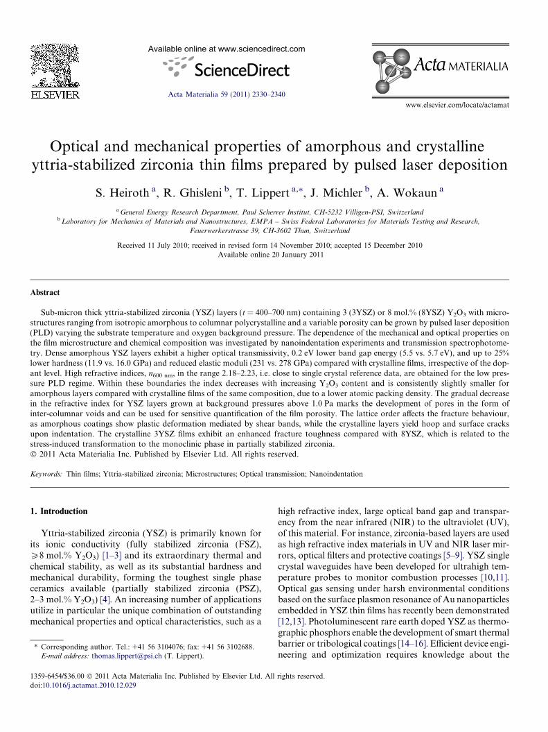
The representative SEM micrographs in Fig. 1 illustratethe major findings of the microstructural dependence of 3and 8 mol.% yttria-stabilized zirconia films on the PLDgrowth parameters, i.e. substrate temperature and oxygenbackground pressure, which has been presented in detailpreviously [25,26]. In the low pressure regime dense layersare obtained, which exhibit either a uniform isotropicstructure in the case of room temperature deposition(Fig. 1a) or an oriented columnar growth at substantiallyhigher substrate temperatures of 400–700 �C (Fig. 1c).Shadowing and collisional moderation of the plume speciescause a transition to open porous structures with spaciousvoids between the columnar features above a thresholdpressure of �2.5 Pa. The effect is particularly pronouncedat low deposition temperatures (Fig. 1b), where insufficientadatom mobility prevents significant structural reorganiza-tion and densification. In addition to the porosity, a lessordered growth and the incorporation of agglomerates(Fig. 1d), presumably formed in the plasma plume, contrib-ute to the observed surface roughening with increasingbackground pressure (compare Table 1). XRD (not shown)
Fig. 1. SEM top view and tilted angle cross-sectional (insets) images of �500 nm7.5 Pa, (c) 600 �C and 1.0 Pa and (d) 600 �C and 7.5 Pa. X-ray diffraction showegrown at 600 �C are polycrystalline.
revealed, moreover, that the layers grown at room temper-ature are amorphous irrespective of the dopant concentra-tion or background pressure. On the other hand, YSZcoatings deposited at 600 �C are polycrystalline, with dif-fraction patterns indicative of the cubic (8YSZ) and tetrag-onal phases (3YSZ) (t0 and t00), respectively.
3.2. Optical properties
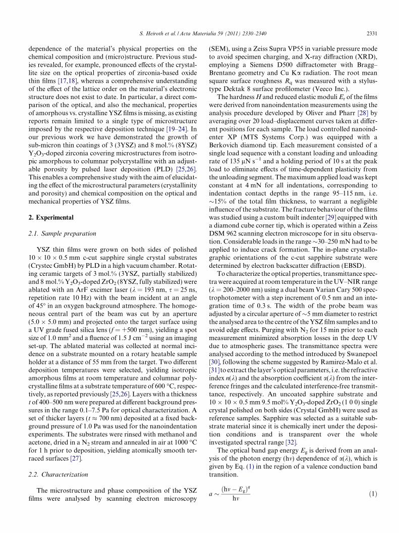
Fig. 2 illustrates the effect of the deposition conditionsand the resulting microstructural characteristics on theUV–visible transmittance spectra for 3YSZ films. The amor-phous layers (Fig. 2a) exhibit a high degree of transparencydown to a wavelength of�300 nm. Below 300 nm they showa weak onset of absorption, followed by a sharp absorptionedge, which is attributed to electronic interband transitions,shifting from�245 nm for dense layers (1.0 Pa) to�215 nmfor porous layers (7.5 Pa). The absorption edge is found at�220 nm for the crystalline YSZ coatings (Fig. 2b), indepen-dent of the deposition conditions. Its appearance at a signif-icantly longer wavelength of �325 nm in the case of a bulk9.5YSZ single crystal, included as a reference in Fig. 2b), isdiscussed later in the context of the optical band gap energy.The crystalline YSZ films (Fig. 2b) reveal, in contrast to theamorphous layers, the development of a broad shoulder ofreduced transmittance in the spectral region 220–500 nm,which is accompanied by a transition from a transparentto an opaque visual appearance. The attenuation of the inci-dent light can be caused by absorption and/or scattering,
thick 3YSZ films deposited by PLD at (a) 25 �C and 1.0 Pa, (b) 25 �C andd that the films deposited at room temperature are amorphous, while those
Table 1Structural data and optical properties for a selection of the YSZ films investigated.
Film pO2(Pa) Rq (A)a t (nm) n600 nm Eg (eV)
c-3YSZ 0.1 4.1 ± 0.3 493 ± 7 2.23 ± 0.02 5.72 ± 0.03c-3YSZ 1.0 5.2 ± 0.8 456 ± 6 2.23 ± 0.02 5.71 ± 0.03c-3YSZ 2.5 6.9 ± 0.7 477 ± 8 2.18 ± 0.02 5.73 ± 0.03c-3YSZ 7.5 56.5 ± 11.3 382 ± 16 n.a. 5.71 ± 0.03a-3YSZ 1.0 6.2 ± 0.5 477 ± 6 2.21 ± 0.02 5.50 ± 0.03a-3YSZ 7.5 73.5 ± 11.5 398 ± 7 1.95 ± 0.02 5.92 ± 0.03c-8YSZ 1.0 5.1 ± 0.7 446 ± 16 2.18 ± 0.02 5.69 ± 0.03a-8YSZ 1.0 5.7 ± 0.7 422 ± 6 2.18 ± 0.02 5.51 ± 0.03
The crystalline layers (index c) were deposited at a substrate temperature of 600 �C, the amorphous ones (index a) without external heating.a For comparison Rq (substrate) = 4.3 ± 0.4 A.
Fig. 2. Transmittance spectra of (a) amorphous and (b) crystalline 3YSZfilms (t = 400–500 nm) deposited on sapphire at different oxygen back-ground pressures in the UV–visual region. Transmittance spectra of anuncoated sapphire substrate and a 9.5YSZ single crystal are included asreferences. The spectra of 8YSZ films are similar and exhibit the samequalitative characteristics.
S. Heiroth et al. / Acta Materialia 59 (2011) 2330–2340 2333
which cannot be separated by transmission mode measure-ments. However, it is unlikely that the absorptivity of thematerial changes significantly as the films’ chemical compo-sition reveals no pronounced variations within the investi-gated range of deposition parameters [25,26]. The missinganalogous behaviour of the amorphous state rather suggeststhat scattering at grain boundaries is mainly responsible forthe additional optical losses. The effect intensifies with theapplied deposition pressure (Fig. 2b) due to the increasinginternal disorder observed in the columnar film structures,as seen in Fig. 1d). Rayleigh theory, which is applicable tosizes of scattering defects much smaller than the wavelength,moreover predicts a k�x (x = 1–3) dependence of the scatter-ing coefficient kscat [33], i.e. the scattering contribution to theextinction coefficient. This accounts qualitatively for theobserved enhancement of the optical losses towards shorterwavelengths. Furthermore, an increase in the scatteringcoefficient due to the increasing surface roughness
kscat � R2q
� �and the incorporation of agglomerates in the
high pressure regime (compare Section 3.1 and Table 1)has to be taken into account.
The amplitude of the interference fringes decreases sig-nificantly with increasing deposition pressure for crystallineas well as amorphous layers, which qualitatively indicates adecrease in the films’ refractive index, since the oscillationamplitude relates to the difference in the refractive indicesof substrate and film. Fig. 3 presents the dispersion of therefractive index as derived from a quantitative analysis ofthe interference patterns for selected 3YSZ and 8YSZ filmsdeposited at two different oxygen background pressuresand, for comparison, a 9.5YSZ single crystal. The refrac-tive index exhibits a plateau in the IR, increases slightlywithin the visible spectral range by �5% and is significantlymore pronounced in the UV. The wavelength dependenceof the refractive index can be described by the expressionn(k) = A + B/k + C/k2 with A, B and C as fitting variables.This trend has previously been observed for YSZ layersdeposited by different techniques, such as spin coating[21] or chemical vapour deposition (CVD) [5], and repre-sents the expected dispersion in the vicinity of the funda-mental absorption band in the deep UV. A comparisonof the refractive index data of the dense films, i.e. those
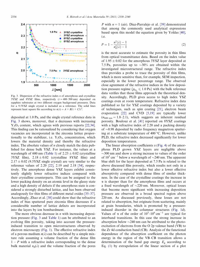
Fig. 3. Dispersion of the refractive index n of amorphous and crystalline3YSZ and 8YSZ films, respectively (t = 400–500 nm) deposited onsapphire substrates at two different oxygen background pressures. Datafor a 9.5YSZ single crystal is included as a reference. The solid linesrepresent least square fits according to n(k) = A + B/k + C/k2.
2334 S. Heiroth et al. / Acta Materialia 59 (2011) 2330–2340
deposited at 1.0 Pa, and the single crystal reference data inFig. 3 shows, moreover, that n decreases with increasingY2O3 content, which agrees with previous reports [22,34].This finding can be rationalized by considering that oxygenvacancies are incorporated in the zirconia lattice propor-tionally to the stabilizer, i.e. Y2O3, concentration, whichlowers the material density and thereby the refractiveindex. The absolute values of n closely match the data pub-lished for dense bulk YSZ. For instance, the values at awavelength of 600 nm (Table 1) of 2.23 ± 0.02 (crystalline3YSZ film), 2.18 ± 0.02 (crystalline 8YSZ film) and2.17 ± 0.02 (9.5YSZ single crystal) are very similar to thereference values of 2.20 [22], 2.19 and 2.18 [34], respec-tively. The amorphous dense YSZ layers exhibit consis-tently slightly lower refractive indices compared withtheir crystalline counterparts. This can be assigned to thelower packing density on an atomic level in the glassy stateand a high density of defects if the amorphous state is con-sidered a strongly disturbed lattice, and has been observedanalogously for thin films of different metal oxides [35–37].Accordingly, Zhao et al. [38] could show that the refractiveindex of bias sputtered pure zirconia films decreases if aconsiderable number of lattice defects are incorporatedinto the layers by ion bombardment.
The more obvious decrease in n with increasing deposi-tion pressure (Fig. 3 and Table 1) can be attributed to anevolving film porosity, taking into account the pressure-induced transition to open microstructures observed byelectron microscopy (Fig. 1). The effective refractive indexof a porous medium n(k) can be described by a simple mix-ture rule assuming a volume fraction of the dense film1 � P with a refractive index corresponding to the densebulk material nd(k) and the volume fraction of the pores
P with n = 1 (air). Diaz-Parralejo et al. [39] demonstratedthat among the commonly used analytical expressionsbased upon this model the equation given by Yoldas [40],i.e.
P ¼ 1� n2ðkÞ � 1
n2dðkÞ � 1
ð2Þ
is the most accurate to estimate the porosity in thin filmsfrom optical transmittance data. Based on the index valueof 1.95 ± 0.02 for the amorphous 3YSZ layer deposited at7.5 Pa, porosities up to �30% are obtained within theinvestigated microstructural range. The refractive indexthus provides a probe to trace the porosity of thin films,which is more sensitive than, for example, SEM inspection,especially in the lower percentage range. The observedclose agreement of the refractive indices in the low deposi-tion pressure regime pO2
6 1:0 Pa� �
with the bulk referencedata verifies that those films approach the theoretical den-sity. Accordingly, PLD gives access to high index YSZcoatings even at room temperature. Refractive index datapublished so far for YSZ coatings deposited by a varietyof techniques, such as spin coating [21], electron beamevaporation [22] and CVD [5,19] are typically lower(n600 nm = 1.8–2.1), which suggests an inherent residualporosity. Boulouz et al. [41] reported on 8YSZ coatingswith a high refractive index of 2.20 and a packing densityof �0.98 deposited by radio frequency magnetron sputter-ing at a substrate temperature of 400 �C. However, unlikePLD, the refractive index decreased significantly for lowerdeposition temperatures.
The linear absorption coefficients a (Fig. 4) of the amor-phous PLD grown YSZ layers are negligible above�300 nm and show a strong increase to values of the orderof 105 cm�1 below a wavelength of �240 nm. The apparentblue shift for the layer deposited at 7.5 Pa is related to theabove discussed film porosity, which results not only in alower effective refractive index but also a lower effectiveabsorptivity compared with dense films of similar thick-ness. In the case of the crystalline coatings the increase ina is sharper than for the amorphous films and occurs ata fixed wavelength of �220 nm. Moreover, optical lossesthat become more significant with increasing depositionpressure are observed in a broad spectral region above220 nm. As discussed previously, these losses are notrelated to absorption, but originate from scattering, mainlyat grain boundaries, which is promoted by a pressure-induced disorder in the columnar structures (Fig. 1d).Values of a of the order of 105–106 cm�1 are typical forinterband transitions. In this case the strong increase inabsorption below �240 nm can be attributed to the photo-excitation of electrons from the O 2p valence band (VB) tothe Zr 4d conduction band (CB). Analysis of the functionaldependence of the absorption coefficient on the photonenergy in the region of the VB–CB transition allows adetermination of the band gap energy Eg according toEq. (1) by extrapolation of the linear section of a plot
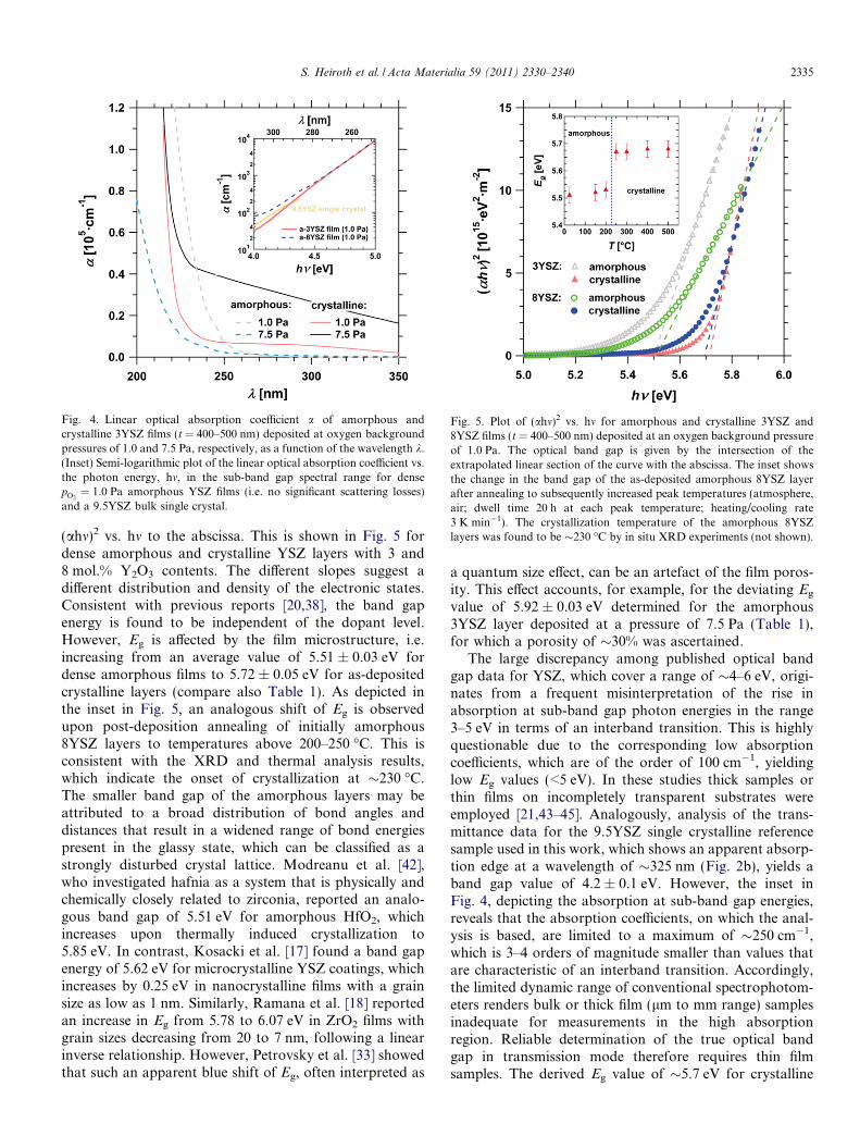
Fig. 4. Linear optical absorption coefficient a of amorphous andcrystalline 3YSZ films (t = 400–500 nm) deposited at oxygen backgroundpressures of 1.0 and 7.5 Pa, respectively, as a function of the wavelength k.(Inset) Semi-logarithmic plot of the linear optical absorption coefficient vs.the photon energy, hm, in the sub-band gap spectral range for densepO2¼ 1:0 Pa amorphous YSZ films (i.e. no significant scattering losses)
and a 9.5YSZ bulk single crystal.
Fig. 5. Plot of (ahm)2 vs. hm for amorphous and crystalline 3YSZ and8YSZ films (t = 400–500 nm) deposited at an oxygen background pressureof 1.0 Pa. The optical band gap is given by the intersection of theextrapolated linear section of the curve with the abscissa. The inset showsthe change in the band gap of the as-deposited amorphous 8YSZ layerafter annealing to subsequently increased peak temperatures (atmosphere,air; dwell time 20 h at each peak temperature; heating/cooling rate3 K min�1). The crystallization temperature of the amorphous 8YSZlayers was found to be �230 �C by in situ XRD experiments (not shown).
S. Heiroth et al. / Acta Materialia 59 (2011) 2330–2340 2335
(ahm)2 vs. hm to the abscissa. This is shown in Fig. 5 fordense amorphous and crystalline YSZ layers with 3 and8 mol.% Y2O3 contents. The different slopes suggest adifferent distribution and density of the electronic states.Consistent with previous reports [20,38], the band gapenergy is found to be independent of the dopant level.However, Eg is affected by the film microstructure, i.e.increasing from an average value of 5.51 ± 0.03 eV fordense amorphous films to 5.72 ± 0.05 eV for as-depositedcrystalline layers (compare also Table 1). As depicted inthe inset in Fig. 5, an analogous shift of Eg is observedupon post-deposition annealing of initially amorphous8YSZ layers to temperatures above 200–250 �C. This isconsistent with the XRD and thermal analysis results,which indicate the onset of crystallization at �230 �C.The smaller band gap of the amorphous layers may beattributed to a broad distribution of bond angles anddistances that result in a widened range of bond energiespresent in the glassy state, which can be classified as astrongly disturbed crystal lattice. Modreanu et al. [42],who investigated hafnia as a system that is physically andchemically closely related to zirconia, reported an analo-gous band gap of 5.51 eV for amorphous HfO2, whichincreases upon thermally induced crystallization to5.85 eV. In contrast, Kosacki et al. [17] found a band gapenergy of 5.62 eV for microcrystalline YSZ coatings, whichincreases by 0.25 eV in nanocrystalline films with a grainsize as low as 1 nm. Similarly, Ramana et al. [18] reportedan increase in Eg from 5.78 to 6.07 eV in ZrO2 films withgrain sizes decreasing from 20 to 7 nm, following a linearinverse relationship. However, Petrovsky et al. [33] showedthat such an apparent blue shift of Eg, often interpreted as
a quantum size effect, can be an artefact of the film poros-ity. This effect accounts, for example, for the deviating Eg
value of 5.92 ± 0.03 eV determined for the amorphous3YSZ layer deposited at a pressure of 7.5 Pa (Table 1),for which a porosity of �30% was ascertained.
The large discrepancy among published optical bandgap data for YSZ, which cover a range of �4–6 eV, origi-nates from a frequent misinterpretation of the rise inabsorption at sub-band gap photon energies in the range3–5 eV in terms of an interband transition. This is highlyquestionable due to the corresponding low absorptioncoefficients, which are of the order of 100 cm�1, yieldinglow Eg values (<5 eV). In these studies thick samples orthin films on incompletely transparent substrates wereemployed [21,43–45]. Analogously, analysis of the trans-mittance data for the 9.5YSZ single crystalline referencesample used in this work, which shows an apparent absorp-tion edge at a wavelength of �325 nm (Fig. 2b), yields aband gap value of 4.2 ± 0.1 eV. However, the inset inFig. 4, depicting the absorption at sub-band gap energies,reveals that the absorption coefficients, on which the anal-ysis is based, are limited to a maximum of �250 cm�1,which is 3–4 orders of magnitude smaller than values thatare characteristic of an interband transition. Accordingly,the limited dynamic range of conventional spectrophotom-eters renders bulk or thick film (lm to mm range) samplesinadequate for measurements in the high absorptionregion. Reliable determination of the true optical bandgap in transmission mode therefore requires thin filmsamples. The derived Eg value of �5.7 eV for crystalline
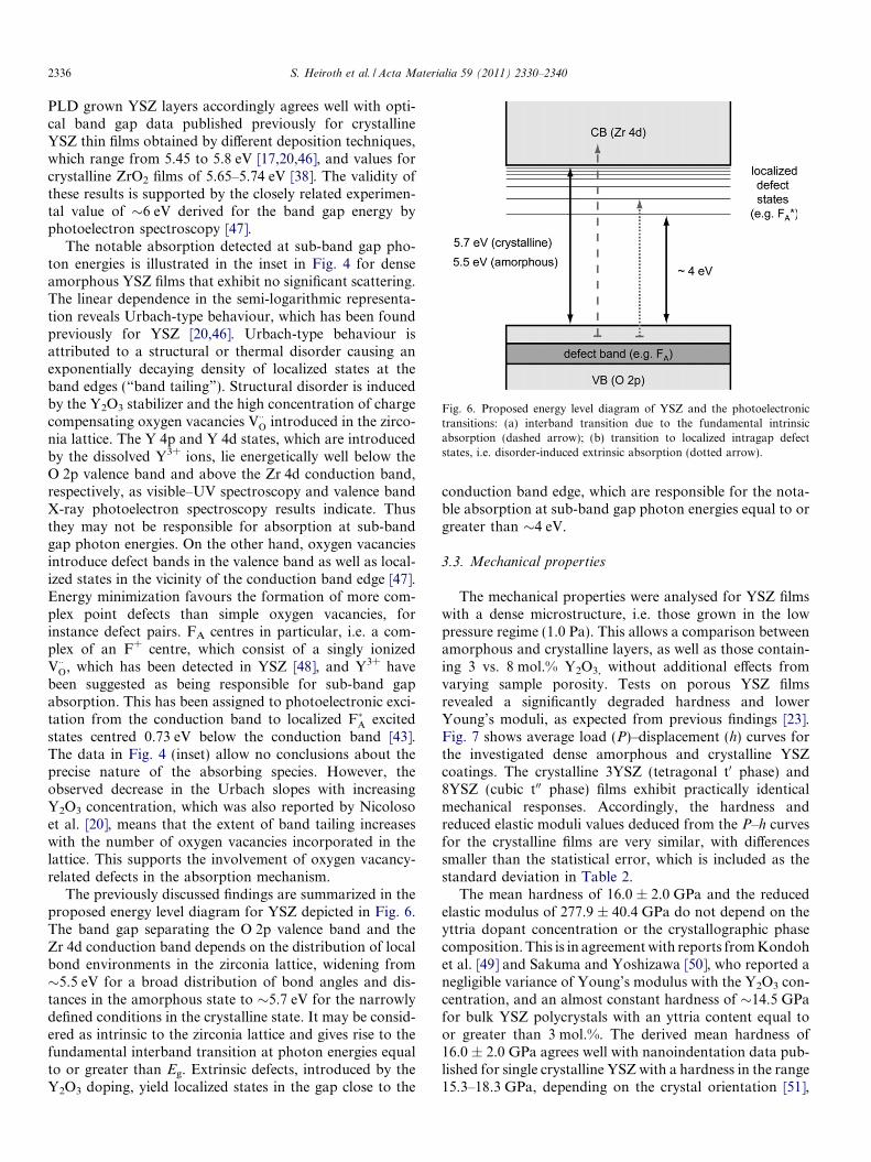
Fig. 6. Proposed energy level diagram of YSZ and the photoelectronictransitions: (a) interband transition due to the fundamental intrinsicabsorption (dashed arrow); (b) transition to localized intragap defectstates, i.e. disorder-induced extrinsic absorption (dotted arrow).
2336 S. Heiroth et al. / Acta Materialia 59 (2011) 2330–2340
PLD grown YSZ layers accordingly agrees well with opti-cal band gap data published previously for crystallineYSZ thin films obtained by different deposition techniques,which range from 5.45 to 5.8 eV [17,20,46], and values forcrystalline ZrO2 films of 5.65–5.74 eV [38]. The validity ofthese results is supported by the closely related experimen-tal value of �6 eV derived for the band gap energy byphotoelectron spectroscopy [47].
The notable absorption detected at sub-band gap pho-ton energies is illustrated in the inset in Fig. 4 for denseamorphous YSZ films that exhibit no significant scattering.The linear dependence in the semi-logarithmic representa-tion reveals Urbach-type behaviour, which has been foundpreviously for YSZ [20,46]. Urbach-type behaviour isattributed to a structural or thermal disorder causing anexponentially decaying density of localized states at theband edges (“band tailing”). Structural disorder is inducedby the Y2O3 stabilizer and the high concentration of chargecompensating oxygen vacancies V��O introduced in the zirco-nia lattice. The Y 4p and Y 4d states, which are introducedby the dissolved Y3+ ions, lie energetically well below theO 2p valence band and above the Zr 4d conduction band,respectively, as visible–UV spectroscopy and valence bandX-ray photoelectron spectroscopy results indicate. Thusthey may not be responsible for absorption at sub-bandgap photon energies. On the other hand, oxygen vacanciesintroduce defect bands in the valence band as well as local-ized states in the vicinity of the conduction band edge [47].Energy minimization favours the formation of more com-plex point defects than simple oxygen vacancies, forinstance defect pairs. FA centres in particular, i.e. a com-plex of an F+ centre, which consist of a singly ionizedV��O, which has been detected in YSZ [48], and Y3+ havebeen suggested as being responsible for sub-band gapabsorption. This has been assigned to photoelectronic exci-tation from the conduction band to localized F�A excitedstates centred 0.73 eV below the conduction band [43].The data in Fig. 4 (inset) allow no conclusions about theprecise nature of the absorbing species. However, theobserved decrease in the Urbach slopes with increasingY2O3 concentration, which was also reported by Nicolosoet al. [20], means that the extent of band tailing increaseswith the number of oxygen vacancies incorporated in thelattice. This supports the involvement of oxygen vacancy-related defects in the absorption mechanism.
The previously discussed findings are summarized in theproposed energy level diagram for YSZ depicted in Fig. 6.The band gap separating the O 2p valence band and theZr 4d conduction band depends on the distribution of localbond environments in the zirconia lattice, widening from�5.5 eV for a broad distribution of bond angles and dis-tances in the amorphous state to �5.7 eV for the narrowlydefined conditions in the crystalline state. It may be consid-ered as intrinsic to the zirconia lattice and gives rise to thefundamental interband transition at photon energies equalto or greater than Eg. Extrinsic defects, introduced by theY2O3 doping, yield localized states in the gap close to the
conduction band edge, which are responsible for the nota-ble absorption at sub-band gap photon energies equal to orgreater than �4 eV.
3.3. Mechanical properties
The mechanical properties were analysed for YSZ filmswith a dense microstructure, i.e. those grown in the lowpressure regime (1.0 Pa). This allows a comparison betweenamorphous and crystalline layers, as well as those contain-ing 3 vs. 8 mol.% Y2O3, without additional effects fromvarying sample porosity. Tests on porous YSZ filmsrevealed a significantly degraded hardness and lowerYoung’s moduli, as expected from previous findings [23].Fig. 7 shows average load (P)–displacement (h) curves forthe investigated dense amorphous and crystalline YSZcoatings. The crystalline 3YSZ (tetragonal t0 phase) and8YSZ (cubic t00 phase) films exhibit practically identicalmechanical responses. Accordingly, the hardness andreduced elastic moduli values deduced from the P–h curvesfor the crystalline films are very similar, with differencessmaller than the statistical error, which is included as thestandard deviation in Table 2.
The mean hardness of 16.0 ± 2.0 GPa and the reducedelastic modulus of 277.9 ± 40.4 GPa do not depend on theyttria dopant concentration or the crystallographic phasecomposition. This is in agreement with reports from Kondohet al. [49] and Sakuma and Yoshizawa [50], who reported anegligible variance of Young’s modulus with the Y2O3 con-centration, and an almost constant hardness of �14.5 GPafor bulk YSZ polycrystals with an yttria content equal toor greater than 3 mol.%. The derived mean hardness of16.0 ± 2.0 GPa agrees well with nanoindentation data pub-lished for single crystalline YSZ with a hardness in the range15.3–18.3 GPa, depending on the crystal orientation [51],
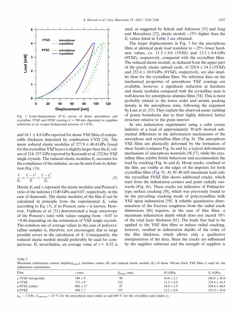
Fig. 7. Load–displacement (P–h) curves of dense amorphous andcrystalline 3YSZ and 8YSZ coatings (t � 700 nm) deposited on sapphiresubstrates at an oxygen background pressure of 1.0 Pa.
S. Heiroth et al. / Acta Materialia 59 (2011) 2330–2340 2337
and 16.1 ± 4.6 GPa reported for dense YSZ films of compa-rable thickness deposited by combustion CVD [24]. Themean reduced elastic modulus of 277.9 ± 40.4 GPa foundfor the crystalline YSZ layers is slightly larger than the Er val-ues of 214–237 GPa reported by Kurosaki et al. [52] for YSZsingle crystals. The reduced elastic modulus Er accounts forthe compliance of the indenter, as can be seen from its defini-tion (Eq. (3)).
1
Er
¼ 1� v2
Eþ 1� v2
i
Ei
ð3Þ
Herein Ei and mi represent the elastic modulus and Poisson’sratio of the indenter (1140 GPa and 0.07, respectively, in thecase of diamond). The elastic modulus of the film E can becalculated in principle from the experimental Er valueaccording to Eq. (3), if its Poisson ratio m is known. How-ever, Fujikane et al. [51] demonstrated a large anisotropyof the Poisson’s ratio with values ranging from �0.07 to+0.80 depending on the orientation of YSZ single crystals.The common use of average values in the case of polycrys-talline samples is, therefore, not encouraged, due to largepossible errors in the calculation of E. Consequently, thereduced elastic moduli should preferably be used for com-parisons. If, nevertheless, an average value of m = 0.32 is
Table 2Maximum indentation contact depths(dindent), hardness values (H) and reduindentation experiments.
Film t (nm) dinden
c-3YSZ (tetragonal) 740 ± 9 98a-3YSZ 713 ± 9 112c-8YSZ (cubic) 696 ± 17 97a-8YSZ 684 ± 7 115
pO2¼ 1:0 Pa, Tsubstrate = 25 �C for the amorphous state (index a) and 600 �C
used, as suggested by Selcuk and Atkinson [53] and Jangand Matsubara [23], elastic moduli �15% higher than theEr values listed in Table 2 are obtained.
The larger displacements in Fig. 7 for the amorphousfilms at identical peak load translate to �25% lower hard-ness values, i.e. 11.5 ± 0.6 (3YSZ) and 12.2 ± 0.4 GPa(8YSZ), respectively, compared with the crystalline films.The reduced elastic moduli, as deduced from the upper partof the purely elastic unload cycle, of 229.4 ± 14.3 (3YSZ)and 232.4 ± 10.0 GPa (8YSZ), respectively, are also smal-ler than for the crystalline films. No reference data on themechanical properties of amorphous YSZ coatings areavailable, however, a significant reduction in hardnessand elastic modulus compared with the crystalline state iswell-known for amorphous alumina films [54]. This is mostprobably related to the lower order and atomic packingdensity in the amorphous state, following the argumentby Lian et al. [55]. They explain the observed easier yieldingof grains boundaries due to their highly defective latticestructure relative to the grain interior.
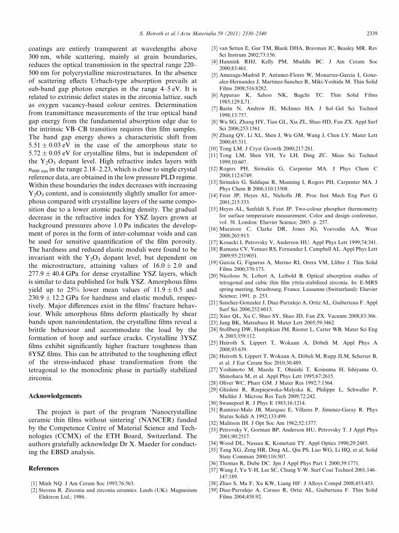
In situ indentation experiments using a cube cornerindenter at a load of approximately 30 mN showed sub-stantial differences in the deformation mechanisms of theamorphous and crystalline films (Fig. 8). The amorphousYSZ films are plastically deformed by the formation ofshear bands (compare Fig. 8a and b), a typical deformationmechanism of amorphous materials [56,57], while the crys-talline films exhibit brittle behaviour and accommodate theload by cracking (Fig. 8c and d). Hoop cracks, confined tothe film, are visible at the edges of the imprints for bothcrystalline films (Fig. 9). At 30–40 mN maximum load onlythe crystalline 8YSZ film shows additional cracks, whichstart from the indentation corners and point radially out-wards (Fig. 8c). These cracks are indicative of Palmqvist-type surface cracking [58], which was previously found tobe the prevailing cracking mode of polycrystalline bulkYSZ upon indentation [59]. A reliable quantitative deter-mination of the fracture toughness from the radial crackdimensions [60] requires, in the case of thin films, amaximum indentation depth which does not exceed 10%of the total layer thickness [61]. The loads that had to beapplied to the YSZ thin films to induce radial cracking,however, resulted in indentation depths of the order ofthe film thickness, which allows only a qualitativeinterpretation of the data. Since the cracks are influencedby the sapphire substrate and the strength of sapphire is
ced elastic moduli (Er) of dense 700 nm thick YSZ films () used for the
t (nm) H (GPa) Er (GPa)
16.0 ± 2.1 260.9 ± 36.011.5 ± 0.6 229.4 ± 14.316.0 ± 1.9 294.8 ± 44.812.2 ± 0.4 232.4 ± 10.0
for the crystalline state (index c).
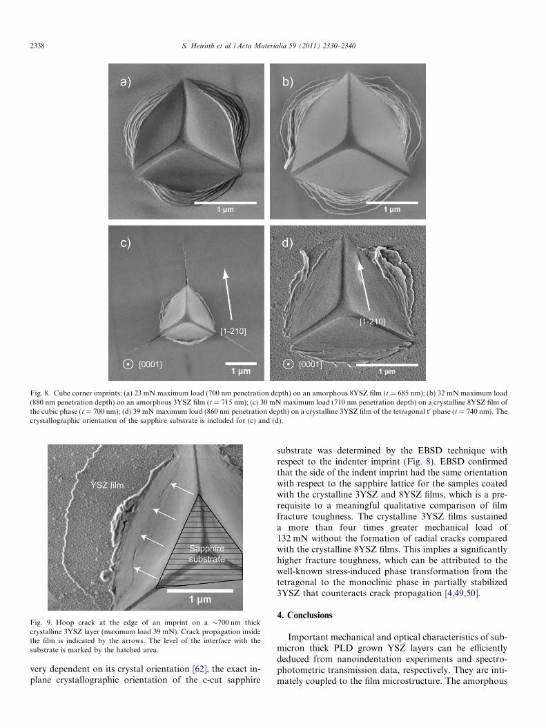
Fig. 8. Cube corner imprints: (a) 23 mN maximum load (700 nm penetration depth) on an amorphous 8YSZ film (t = 685 nm); (b) 32 mN maximum load(880 nm penetration depth) on an amorphous 3YSZ film (t = 715 nm); (c) 30 mN maximum load (710 nm penetration depth) on a crystalline 8YSZ film ofthe cubic phase (t = 700 nm); (d) 39 mN maximum load (860 nm penetration depth) on a crystalline 3YSZ film of the tetragonal t0 phase (t = 740 nm). Thecrystallographic orientation of the sapphire substrate is included for (c) and (d).
Fig. 9. Hoop crack at the edge of an imprint on a �700 nm thickcrystalline 3YSZ layer (maximum load 39 mN). Crack propagation insidethe film is indicated by the arrows. The level of the interface with thesubstrate is marked by the hatched area.
2338 S. Heiroth et al. / Acta Materialia 59 (2011) 2330–2340
very dependent on its crystal orientation [62], the exact in-plane crystallographic orientation of the c-cut sapphire
substrate was determined by the EBSD technique withrespect to the indenter imprint (Fig. 8). EBSD confirmedthat the side of the indent imprint had the same orientationwith respect to the sapphire lattice for the samples coatedwith the crystalline 3YSZ and 8YSZ films, which is a pre-requisite to a meaningful qualitative comparison of filmfracture toughness. The crystalline 3YSZ films sustaineda more than four times greater mechanical load of132 mN without the formation of radial cracks comparedwith the crystalline 8YSZ films. This implies a significantlyhigher fracture toughness, which can be attributed to thewell-known stress-induced phase transformation from thetetragonal to the monoclinic phase in partially stabilized3YSZ that counteracts crack propagation [4,49,50].
4. Conclusions
Important mechanical and optical characteristics of sub-micron thick PLD grown YSZ layers can be efficientlydeduced from nanoindentation experiments and spectro-photometric transmission data, respectively. They are inti-mately coupled to the film microstructure. The amorphous
S. Heiroth et al. / Acta Materialia 59 (2011) 2330–2340 2339
coatings are entirely transparent at wavelengths above300 nm, while scattering, mainly at grain boundaries,reduces the optical transmission in the spectral range 220–500 nm for polycrystalline microstructures. In the absenceof scattering effects Urbach-type absorption prevails atsub-band gap photon energies in the range 4–5 eV. It isrelated to extrinsic defect states in the zirconia lattice, suchas oxygen vacancy-based colour centres. Determinationfrom transmittance measurements of the true optical bandgap energy from the fundamental absorption edge due tothe intrinsic VB–CB transition requires thin film samples.The band gap energy shows a characteristic shift from5.51 ± 0.03 eV in the case of the amorphous state to5.72 ± 0.05 eV for crystalline films, but is independent ofthe Y2O3 dopant level. High refractive index layers withn600 nm in the range 2.18–2.23, which is close to single crystalreference data, are obtained in the low pressure PLD regime.Within these boundaries the index decreases with increasingY2O3 content, and is consistently slightly smaller for amor-phous compared with crystalline layers of the same compo-sition due to a lower atomic packing density. The gradualdecrease in the refractive index for YSZ layers grown atbackground pressures above 1.0 Pa indicates the develop-ment of pores in the form of inter-columnar voids and canbe used for sensitive quantification of the film porosity.The hardness and reduced elastic moduli were found to beinvariant with the Y2O3 dopant level, but dependent onthe microstructure, attaining values of 16.0 ± 2.0 and277.9 ± 40.4 GPa for dense crystalline YSZ layers, whichis similar to data published for bulk YSZ. Amorphous filmsyield up to 25% lower mean values of 11.9 ± 0.5 and230.9 ± 12.2 GPa for hardness and elastic moduli, respec-tively. Major differences exist in the films’ fracture behav-iour. While amorphous films deform plastically by shearbands upon nanoindentation, the crystalline films reveal abrittle behaviour and accommodate the load by theformation of hoop and surface cracks. Crystalline 3YSZfilms exhibit significantly higher fracture toughness than8YSZ films. This can be attributed to the toughening effectof the stress-induced phase transformation from thetetragonal to the monoclinic phase in partially stabilizedzirconia.
Acknowledgements
The project is part of the program ‘Nanocrystallineceramic thin films without sintering’ (NANCER) fundedby the Competence Centre of Material Science and Tech-nologies (CCMX) of the ETH Board, Switzerland. Theauthors gratefully acknowledge Dr X. Maeder for conduct-ing the EBSD analysis.
References
[1] Minh NQ. J Am Ceram Soc 1993;76:563.[2] Stevens R. Zirconia and zirconia ceramics. Leeds (UK): Magnesium
Elektron Ltd.; 1986.
[3] van Setten E, Gur TM, Blank DHA, Bravman JC, Beasley MR. RevSci Instrum 2002;73:156.
[4] Hannink RHJ, Kelly PM, Muddle BC. J Am Ceram Soc2000;83:461.
[5] Amezaga-Madrid P, Antunez-Flores W, Monarrez-Garcia I, Gonz-alez-Hernandez J, Martinez-Sanchez R, Miki-Yoshida M. Thin SolidFilms 2008;516:8282.
[6] Apparao K, Sahoo NK, Bagchi TC. Thin Solid Films1985;129:L71.
[7] Bazin N, Andrew JE, McInnes HA. J Sol–Gel Sci Technol1998;13:757.
[8] Wu SG, Zhang HY, Tian GL, Xia ZL, Shao HD, Fan ZX. Appl SurfSci 2006;253:1561.
[9] Zhang QY, Li XL, Shen J, Wu GM, Wang J, Chen LY. Mater Lett2000;45:311.
[10] Tong LM. J Cryst Growth 2000;217:281.[11] Tong LM, Shen YH, Ye LH, Ding ZC. Meas Sci Technol
1999;10:607.[12] Rogers PH, Sirinakis G, Carpenter MA. J Phys Chem C
2008;112:6749.[13] Sirinakis G, Siddique R, Manning I, Rogers PH, Carpenter MA. J
Phys Chem B 2006;110:13508.[14] Feist JP, Heyes AL, Nicholls JR. Proc Inst Mech Eng Part G
2001;215:333.[15] Heyes AL, Seefeldt S, Feist JP. Two-colour phosphor thermometry
for surface temperature measurement. Color and design conference,vol. 38. London: Elsevier Science; 2003. p. 257.
[16] Muratore C, Clarke DR, Jones JG, Voevodin AA. Wear2008;265:913.
[17] Kosacki I, Petrovsky V, Anderson HU. Appl Phys Lett 1999;74:341.[18] Ramana CV, Vemuri RS, Fernandez I, Campbell AL. Appl Phys Lett
2009;95:2319051.[19] Garcia G, Figueras A, Merino RI, Orera VM, Llibre J. Thin Solid
Films 2000;370:173.[20] Nicoloso N, Lobert A, Leibold B. Optical absorption studies of
tetragonal and cubic thin film yttria-stabilized zirconia. In: E-MRSspring meeting, Strasbourg, France. Lausanne (Switzerland): ElsevierScience; 1991. p. 253.
[21] Sanchez-Gonzalez J, Diaz-Parralejo A, Ortiz AL, Guiberteau F. ApplSurf Sci 2006;252:6013.
[22] Xiao QL, Xu C, Shao SY, Shao JD, Fan ZX. Vacuum 2008;83:366.[23] Jang BK, Matsubara H. Mater Lett 2005;59:3462.[24] Stollberg DW, Hampikian JM, Riester L, Carter WB. Mater Sci Eng
A 2003;359:112.[25] Heiroth S, Lippert T, Wokaun A, Dobeli M. Appl Phys A
2008;93:639.[26] Heiroth S, Lippert T, Wokaun A, Dobeli M, Rupp JLM, Scherrer B,
et al. J Eur Ceram Soc 2010;30:489.[27] Yoshimoto M, Maeda T, Ohnishi T, Koinuma H, Ishiyama O,
Shinohara M, et al. Appl Phys Lett 1995;67:2615.[28] Oliver WC, Pharr GM. J Mater Res 1992;7:1564.[29] Ghisleni R, Rzepiejewska-Malyska K, Philippe L, Schwaller P,
Michler J. Microsc Res Tech 2009;72:242.[30] Swanepoel R. J Phys E 1983;16:1214.[31] Ramirez-Malo JB, Marquez E, Villares P, Jimenez-Garay R. Phys
Status Solidi A 1992;133:499.[32] Malitson IH. J Opt Soc Am 1962;52:1377.[33] Petrovsky V, Gorman BP, Anderson HU, Petrovsky T. J Appl Phys
2001;90:2517.[34] Wood DL, Nassau K, Kometani TY. Appl Optics 1990;29:2485.[35] Tang XG, Zeng HR, Ding AL, Qiu PS, Luo WG, Li HQ, et al. Solid
State Commun 2000;116:507.[36] Thomas R, Dube DC. Jpn J Appl Phys Part 1 2000;39:1771.[37] Wang J, Yu Y-H, Lee SC, Chung Y-W. Surf Coat Technol 2001;146–
147:189.[38] Zhao S, Ma F, Xu KW, Liang HF. J Alloys Compd 2008;453:453.[39] Diaz-Parralejo A, Caruso R, Ortiz AL, Guiberteau F. Thin Solid
Films 2004;458:92.
2340 S. Heiroth et al. / Acta Materialia 59 (2011) 2330–2340
[40] Yoldas BE. Appl Optics 1980;19:1425.[41] Boulouz M, Boulouz A, Giani A, Boyer A. Thin Solid Films
1998;323:85.[42] Modreanu M, Sancho-Parramon J, Durand O, Servet B, Stchakovsky
M, Eypert C, et al. Investigation of thermal annealing effects onmicrostructural and optical properties of HfO2 thin films. In: E-MRSspring meeting, Strasbourg, France. Lausanne (Switzerland): ElsevierScience; 2005. p. 328.
[43] Paiverneker VR, Petelin AN, Crowne FJ, Nagle DC. Phys Rev B1989;40:8555.
[44] Pang GS, Chen SG, Zhu YC, Palchik O, Koltypin Y, Zaban A, et al.J Phys Chem B 2001;105:4647.
[45] Preusser S, Stimming U, Wippermann K. An optical and electro-chemical investigation of ZrO2 thin films (from nm to mm thickness).In: 44th Meeting of the International Society of Electrochemis-try. Berlin: Pergamon-Elsevier Science; 1994. p. 1273.
[46] Camagni P, Galinetto P, Samoggia G, Zema N. Solid State Commun1992;83:943.
[47] French RH, Glass SJ, Ohuchi FS, Xu YN, Ching WY. Phys Rev B1994;49:5133.
[48] Costantini JM, Beuneu F, Gourier D, Trautmann C, Calas G,Toulemonde M. J Phys: Condens Matter 2004;16:3957.
[49] Kondoh J, Shiota H, Kawachi K, Nakatani T. J Alloys Compd2004;365:253.
[50] Sakuma T, Yoshizawa YI. J Mater Sci 1985;20:2399.[51] Fujikane M, Setoyama D, Nagao S, Nowak R, Yamanaka S. J Alloys
Compd 2007;431:250.[52] Kurosaki K, Setoyama D, Matsunaga JJ, Yamanaka S. J Alloys
Compd 2005;386:261.[53] Selcuk A, Atkinson A. J Am Ceram Soc 2000;83:2029.[54] Alcala G, Skeldon P, Thompson GE, Mann AB, Habazaki H,
Shimizu K. Nanotechnology 2002;13:451.[55] Lian J, Garay JE, Wang JL. Scr Mater 2007;56:1095.[56] Kim JJ, Choi Y, Suresh S, Argon AS. Science 2002;295:654.[57] Moser B, Loffler JF, Michler J. Discrete deformation in
amorphous metals: an in situ SEM indentation study. In:Conference on instrumented indentation testing in materialsresearch and development, Iraklion, Greece. London: Taylor &Francis; 2005. p. 5715.
[58] Niihara K, Morena R, Hasselman DPH. J Mater Sci Lett 1982;1:13.
[59] Jones SL, Norman CJ, Shahani R. J Mater Sci Lett 1987;6:721.[60] Volinsky AA, Vella JB, Gerberich WW. Thin Solid Films
2003;429:201.[61] Li X, Diao D, Bhushan B. Acta Mater 1997;45:4453.[62] Schmid F, Harris DC. J Am Ceram Soc 1998;81:885.