optical and structural properties of si nanocrystals in sio2 films
TRANSCRIPT
https://helda.helsinki.fi
Optical and Structural Properties of Si Nanocrystals in SiO2 Films
Nikitin, Timur
2015-06
Nikitin , T & Khriachtchev , L 2015 , ' Optical and Structural Properties of Si Nanocrystals in
SiO2 Films ' , Nanomaterials , vol. 5 , no. 2 , pp. 614-655 . https://doi.org/10.3390/nano5020614
http://hdl.handle.net/10138/159315
https://doi.org/10.3390/nano5020614
Downloaded from Helda, University of Helsinki institutional repository.
This is an electronic reprint of the original article.
This reprint may differ from the original in pagination and typographic detail.
Please cite the original version.
Nanomaterials 2015, 5, 614-655; doi:10.3390/nano5020614
nanomaterials ISSN 2079-4991
www.mdpi.com/journal/nanomaterials
Review
Optical and Structural Properties of Si Nanocrystals in SiO2 Films
Timur Nikitin and Leonid Khriachtchev *
Department of Chemistry, University of Helsinki, P.O. Box 55, FI-00014 Helsinki, Finland;
E-Mail: [email protected]
* Author to whom correspondence should be addressed; E-Mail: [email protected];
Tel.: +358 294150310.
Academic Editor: Lorenzo Rosa
Received: 4 March 2015 / Accepted: 10 April 2015 / Published: 22 April 2015
Abstract: Optical and structural properties of Si nanocrystals (Si-nc) in silica films are
described. For the SiOx (x < 2) films annealed above 1000 °C, the Raman signal of Si-nc
and the absorption coefficient are proportional to the amount of elemental Si detected by
X-ray photoelectron spectroscopy. A good agreement is found between the measured
refractive index and the value estimated by using the effective-medium approximation. The
extinction coefficient of elemental Si is found to be between the values of crystalline and
amorphous Si. Thermal annealing increases the degree of Si crystallization; however, the
crystallization and the Si–SiO2 phase separation are not complete after annealing at
1200 °C. The 1.5-eV PL quantum yield increases as the amount of elemental Si decreases;
thus, this PL is probably not directly from Si-nc responsible for absorption and detected by
Raman spectroscopy. Continuous-wave laser light can produce very high temperatures in
the free-standing films, which changes their structural and optical properties. For relatively
large laser spots, the center of the laser-annealed area is very transparent and consists of
amorphous SiO2. Large Si-nc (up to ∼300 nm in diameter) are observed in the ring around
the central region. These Si-nc lead to high absorption and they are typically under
compressive stress, which is connected with their formation from the liquid phase. By
using strongly focused laser beams, the structural changes in the free-standing films can be
made in submicron areas.
Keywords: Si nanocrystal (Si-nc); SiO2 film; Raman spectroscopy; photoluminescence;
laser annealing
OPEN ACCESS
Nanomaterials 2015, 5 615
1. Introduction
Many limitations of modern electronic devices may be overcome by implementing photonics into
electronics [1–4]. Integration of Si-based photonics with CMOS technology is a promising approach
because it gives the possibility to merge electronics and photonics in the same chip [5–9]. Many
optical functions such as, for example, light sources, amplifiers, waveguides, modulators, memory, and
detectors should be achieved in order to fulfill this integration. Realization of a true monolithically
fabricated injection Si laser with a small size is a particularly challenging task. The fundamental
problem is the low light-emitting efficiency of bulk silicon due to its indirect band gap (~1.1 eV),
which leads to long radiative times (~ms) and therefore, mostly non-radiative recombination of the
excited carriers. The efficiency of the light emission can be enhanced by increasing the overlap of the
wave functions of the electron and hole via, for example, spatial confinement [10–13]. The unusual
properties of Si structures are observed when the size is less than the free exciton Bohr radius of
4.3 nm in bulk Si. This quantum confinement (QC) effect leads to the following main changes in the
material properties: (i) an increase of the radiative probability due to delocalization of the wave
functions in the momentum space, which increases the electron-hole wave function overlap and (ii) a
shift in the emission wavelength to the visible region due to an increase of the band gap, which is
controlled by the Si nanostructure size. Moreover, the number of sites within the volume of Si
nanostructures, where non-radiative recombination can occur, decreases considerably. It should be
mentioned that understanding electrical transport mechanisms in the systems considered below is very
important for many applications [14]; however, this topic is outside the scope of the present review.
Porous Si is the first example of a Si-based material with enhanced luminescence efficiency. Strong
room-temperature photoluminescence (PL) in visible spectral region from this material was discovered
by Leigh Canham in 1990 [15]. Visible luminescence ranging from green to red in color was soon
reported by Canham et al. [16] for other porous-Si samples and by other researchers [17,18] and
ascribed to the quantum effects in Si structures with a size of ~3 nm. The blue shift of the PL and
optical absorption with the increasing porosity (decreasing Si nanocluster sizes) provided the first
important evidence that the QC plays an important role in light emission from porous Si. This blue
shift is a result of the band gap expansion controlled by the size of Si nanostructures [13,19].
It was soon understood that oxidation of small Si crystallites has a great influence on the light
emission [20,21]. The study by Wolkin et al. of oxidized porous Si has shown that the light-emitting
centers can involve the Si=O covalent bonds located on the crystallite surface [22]. For oxygen-passivated
Si crystallites, a stabilized electronic surface state is formed on a Si=O covalent bond and various
recombination mechanisms can operate depending on the crystallite size. For larger sizes (>3 nm),
recombination occurs via free excitons since the band gap is not wide enough to stabilize the Si=O
surface state. For intermediate sizes (~2.5 nm), recombination involves a trapped electron localized on
the Si atom of the Si=O bond and a free hole. For smaller sizes (<2 nm), recombination occurs via
trapped excitons.
However, QC has been demonstrated for a number of Si nanomaterials. In contrast with oxygen
passivation, for hydrogen-passivated porous Si, recombination occurs via free exciton states for all
crystallite sizes and follows the expected QC behavior [22]. Ledoux et al. studied Si nanocrystals
(Si-nc) prepared by pulsed CO2 laser pyrolysis of silane in a gas flow reactor and deposited on a
Nanomaterials 2015, 5 616
substrate [23]. It was observed that the PL band was blue-shifted as the size of Si-nc decreased from
8 to 2.5 nm. This dependence clearly follows the QC model. The QC mechanism operates also for
alkane-terminated Si-nc. Hannah et al. [24] convincingly demonstrated using pressure-dependent PL
studies that the PL arises from the core-states of Si-nc with indirect-gap transitions. The same PL
mechanism has also been reported to operate for Si-nc in silicon-nitride films [25,26].
Another attractive Si-based material, which is the focus of the present article, is composed of Si-nc
embedded in a SiO2 matrix. This material is chemically and mechanically more stable compared to
porous Si and also emits light in the visible region. Si-nc in silica films can be prepared by various
methods such as, for example, molecular beam deposition (MBD) [27,28], Si-ion implantation [29–32],
sputtering [33–39], plasma enhanced chemical vapor deposition (PECVD) [33,34,40–42], low pressure
chemical vapor deposition with subsequent thermal oxidation [43–45], reactive evaporation of SiO
powder in oxygen atmosphere [46], and electron beam deposition [47]. Two types of architectures are
most commonly prepared: (i) Si-rich silicon oxide SiOx (x < 2) films [31,33,40,48,49] and
(ii) SiOx/SiO2 [37,46,47,50–53] and Si/SiO2 [27,28,35,54–57] superlattices (SLs). Si-nc are formed in
these materials by furnace annealing above 1000 °C. Studies of Si-nc in SiO2 have been particularly
stimulated by the observation of optical gain in this material [58,59]. In addition to PL,
electroluminescence in visible region from porous Si and from Si-nc in SiO2 has been reported [60,61].
The origin of light emission from Si-nc in a SiO2 matrix is still controversial. It seems that the
conclusions on the mechanism of the light emission from oxidized porous Si [20–22,62] are relevant to
Si-nc in SiO2. Similarly, the PL of Si-nc (sizes > 3 nm) in SiO2 can be ascribed to the QC effect [63–66].
On the other hand, the importance of the Si-nc/SiO2 interface in the light-emitting properties has been
stressed [31,35,67,68] and, in particular, the defect origin of the PL has been discussed [27,29,31,69–71].
Godefroo et al. have convincingly demonstrated that defects are the dominant source of the 1.5-eV PL [52].
In their experiment, an amorphous SiO/SiO2 SL grown by reactive evaporation of SiO powders in an
oxygen atmosphere was thermally annealed at 1100 °C for 1 h under N2 atmosphere to produce Si-nc.
The authors could switch the PL mechanism between the QC and defect mechanisms by passivation
with hydrogen and ultraviolet illumination, respectively.
Optoelectronic applications of Si-based materials require knowledge of their optical and structural
properties. For SiOx (x < 2) films prepared by PECVD, the energy-filtered transmission electron
microscopy (EFTEM) show that the Si–SiO2 phase separation starts after annealing at 900 °C for
1 h under N2 atmosphere when Si clusters become visible in an oxide matrix [72]. The dark-field (DF)
transmission electron microscopy (TEM) technique reliably shows that the Si clusters are amorphous
for annealing temperatures of 900–1000 °C, and their crystallization begins at 1100 °C. Higher
annealing temperatures promote further crystallization of the Si clusters. The Si-nc size as a function
of the annealing temperature and Si content has been studied for samples prepared by different
deposition methods. For samples prepared by PECVD, the TEM results indicate that the Si-nc sizes
increase with the increasing annealing temperature for a given Si content and with the Si content for a
given annealing temperature [40]. The increase of the Si-nc sizes with the annealing temperature is also
observed for SiOx films grown by magnetron sputtering [37]. For SiOx films prepared by ion
implantation, the nucleation and pure growth stages of the nanocrystal population are almost over after
1 min of annealing at 1100 °C in N2 [31]. For longer annealing periods, the sizes of Si-nc increase due
to coalescence or Ostwald ripening process [31,73].
Nanomaterials 2015, 5 617
Several methods have been employed to study optical constants of different materials
containing Si-nc. These methods include, for example, optical ellipsometry [74–76] and m-line
measurements [77–79]. The analysis of the optical properties often uses the Bruggeman effective-medium
approximation [80–82]. The Tauc-Lorentz model provides optical constants of Si-nc deposited on a
substrate [82]. The results show that the optical properties of Si-nc are quite different from those of
amorphous and crystalline Si. It has been found that at a given wavelength, the refractive index of SiOx
films increases for larger Si-nc for Si-ion implanted samples [74] and for larger Si content for PCVD
samples [75]. Chen et al. have developed a quantitative approach of obtaining depth profiles of the
optical constants [81]. Moreno et al. report that the refractive index of Si-nc is lower than that of
amorphous and crystalline bulk Si [80]. They also conclude that the refractive index is rather
independent of the Si clusters sizes (3.6–4.6 nm) and is mostly affected by the degree of crystallinity.
For SiOx/SiO2 SLs prepared by magnetron sputtering, negative optical birefringence (~1%) was
observed, originating from the periodical set of parallel planes of two different materials constituting
the SL [77,78]. At a given wavelength, the absorption coefficient of annealed SiOx films prepared by
magnetron sputtering and PECVD increases with the Si content [33,76,83]. The increase of the Si-nc
mean diameter leads to an increase of absorption in porous Si [84] and in SiOx films prepared by ion
implantation [80]. For a fixed Si content, the absorption coefficient of films prepared by magnetron
sputtering and PECVD decreases with the increasing annealing temperature, which is due the
amorphous-to-crystalline transition of Si in the samples [33].
Another method of measuring the optical properties of SiOx films is based on the PL-filtering effect.
A silicon oxide layer containing Si-nc on a silica substrate forms a planar waveguide. Spectral filtering
of the PL occurs when the PL is detected from the waveguide edge along the film surface. This effect
has been found for Si/SiO2 SLs [57] and for SiOx films (x < 2) on silica substrate [79,85–87]. The
detailed description of this effect is presented later.
The Tauc relation [88] allows one to estimate the band gap of SiOx films containing
Si-nc [31,33,36,44,74,89,90]. A study of Si-nc deposited on a silica substrate shows that the electronic
band structure of Si-nc is quite different from that of bulk silicon and that the band gap increases as the
Si-nc size decreases [82]. The latter observation is explained by the QC effect. The increase of the
band gap for smaller Si-nc is also observed for implanted SiOx samples [31,74]. The
absorption threshold is blue-shifted for smaller Si-nc, which indicates the QC effect on the Si-nc band
gap [33,36,84,90,91].
Laser annealing is an interesting approach to change the structural and optical properties of Si-based
materials. The heating effect of pulsed radiation is especially strong [92]. However, it can also be
substantial for continuous-wave (CW) irradiation of free-standing porous Si films [93]. A similar
heating effect of CW laser radiation is observed in free-standing SiOx films leading to a strong increase
of the Raman signal of Si-nc [56,94–96]. Si-nc prepared by laser annealing show high compressive
stress (~3 GPa), which is evidenced by an up-shift of the Raman band [56,96]. The compressive stress
is formed in a solid SiO2 matrix when the volume of Si-nc suddenly increases after its crystallization
from the liquid phase. The high stress can be relaxed by irradiating the stressed Si-nc with lower laser
power [56]. Free-standing films are used to obtain the above described laser-induced effects because
for films on substrates the laser-induced heat is reduced due to thermal flux to substrate [97]; however,
it is still observable [98].
Nanomaterials 2015, 5 618
In agreement with the experimental observations, the theoretical simulations of isolated
hydrogen-passivated Si nanostructures show that the band gap and the PL peak position change
according to QC [13,19]. The behavior of these parameters is different for oxidized Si-nc [99].
Theoretical studies highlight the importance of the interface region between Si-nc and a SiO2 matrix
for the light-emitting properties [100,101]. The absorption edge tends to be red-shifted due to the
formation of the Si=O or Si–O–Si bonds at the Si/SiO2 interface [102–104]. The presence of oxygen
atoms bonded to the surface of Si-nc as well as deformation of Si-nc are found to influence the optical
band gap [105]. Luppi et al. have considered small Si-nc (up to 1 nm in diameter) by applying
ab initio calculations [106]. In the case of the Si–O–Si bridge bond at the cluster surface, an emission
peak at about 1.5 eV is obtained. In accord, the PL in this region is often observed experimentally from
silica films containing Si-nc. The calculated emission peak is red-shifted with respect to the
absorption, which is also in agreement with the experimentally observed Stokes shifts between the
absorption and PL spectra.
Theoretical calculations show that the surrounding matrix can produce some strain on Si-nc [107–109],
and this strain depends on the oxidation degree [110,111]. The magnitude of strain affects the band
gap, which shows an oscillating behavior with the Si-nc size, not strictly following the QC rule [110].
Moreover, the disorder of nanoclusters has a large effect on their optoelectronic properties [112,113].
In particular, amorphization reduces the optical band gap and increases the absorption strength in the
visible range.
Guerra and Ossicini have calculated the recombination rates for different classes of Si-nc in the
diameter range of 0.2–1.5 nm [114]. The authors also consider different conditions of passivation,
strain, and symmetry in order to find the best conditions of radiative emission. As a result, they
have found that the smallest, highly oxidized, crystalline clusters are the most optically active
Si/SiO2 structures.
2. Results and Discussion
2.1. Furnace-Annealed Films
In this section, we describe the properties of SiOx (x < 2) films on silica substrates for different
annealing temperatures (400–1200 °C) and Si contents (x from ~1.3 to ~1.98) [115–118]. The SiOx
films (thickness from ~1.5 to ~2.5 μm) are deposited on silica substrates by MBD. The MBD samples
are compared with samples prepared by ion implantation [118].
2.1.1. Correlation between Optical and Structural Properties
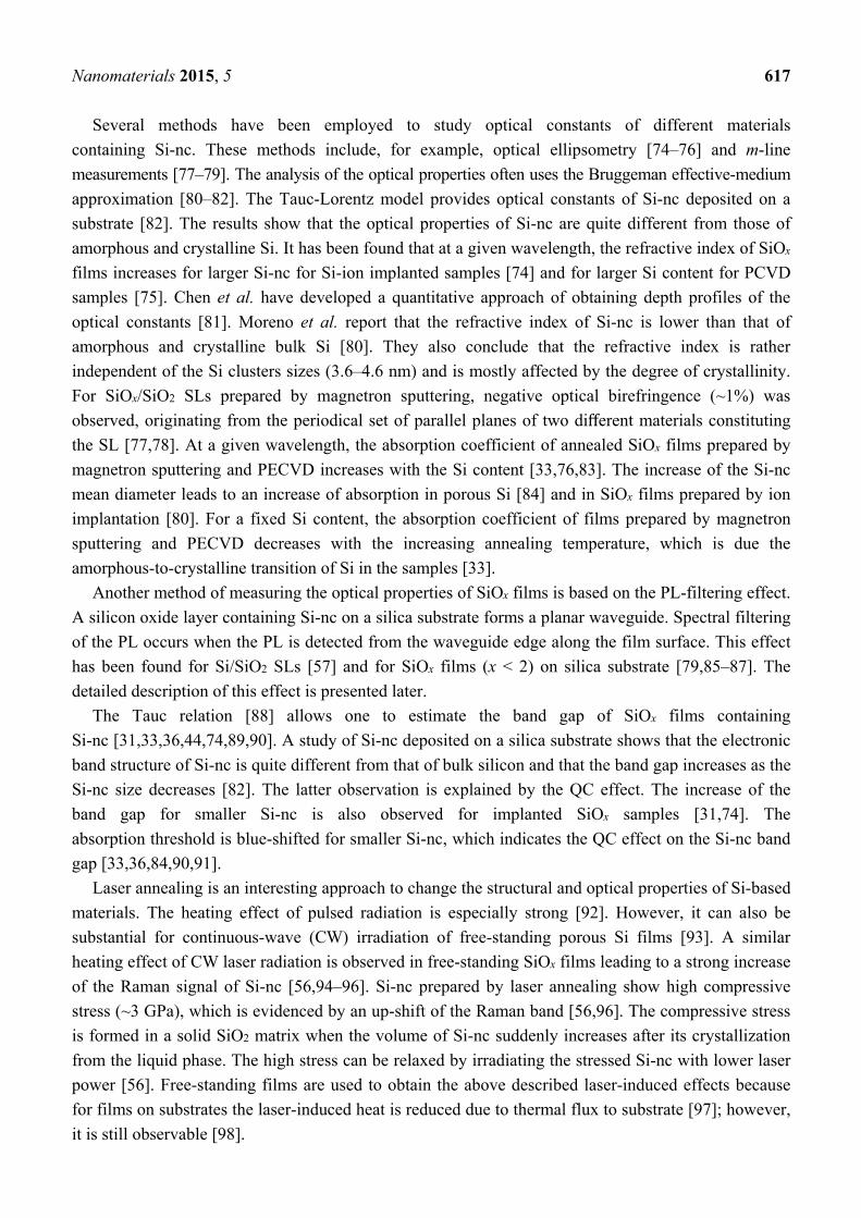
The as-prepared MBD films (annealed at 400 °C for better mechanical stability) with substantial Si
content show a broad Raman band at ~470 cm–1, which is characteristic of amorphous Si
(Figure 1) [27,48,55,119,120]. After annealing above 1000 °C, crystallization of the amorphous Si
inclusions occurs as evidenced by the narrowing and upshift of the Raman band to ~518 cm–1
(Figure 1). When measured with low laser intensity, the Raman band position (518–519 cm–1) is rather
independent of the Si content and of the annealing temperature in the 1100–1200 °C range. According
to the phonon confinement model [121,122], this result suggests that the Si-nc sizes evidenced by
Nanomaterials 2015, 5 619
Raman spectroscopy do not change much under these conditions. However, growth of Si-nc
with increasing annealing temperature was observed for SiOx films prepared by other deposition
methods [37,40].
For MBD SiOx films with very small excess of Si (x > 1.9), the Raman bands of amorphous and
crystalline Si are nearly invisible [116], in qualitative agreement with the earlier results [27]. The
reason for this observation is the small amount of properly coordinated Si atoms (Si atoms bonded to
four “bulk” Si atoms) for samples with low Si contents. A similar explanation was applied in a study of
amorphous Si/SiO2 SLs, where the Raman bands of amorphous Si were observed for thicker Si layers
(≥2 nm) and the Raman-scattering cross section decreased for thinner Si layers [55,123].
As the annealing temperature increases, the low-frequency shoulder in the Raman spectra
responsible for disordered Si and/or small Si clusters gradually decreases (Figure 1). However, even
after annealing at 1200 °C, the low-frequency component of the Raman band does not disappear and
its area is comparable to that of the high-frequency component. As a possibility, small Si grains
in a SiO2 matrix may be disordered even after annealing at this temperature whereas larger Si grains
are crystallized.
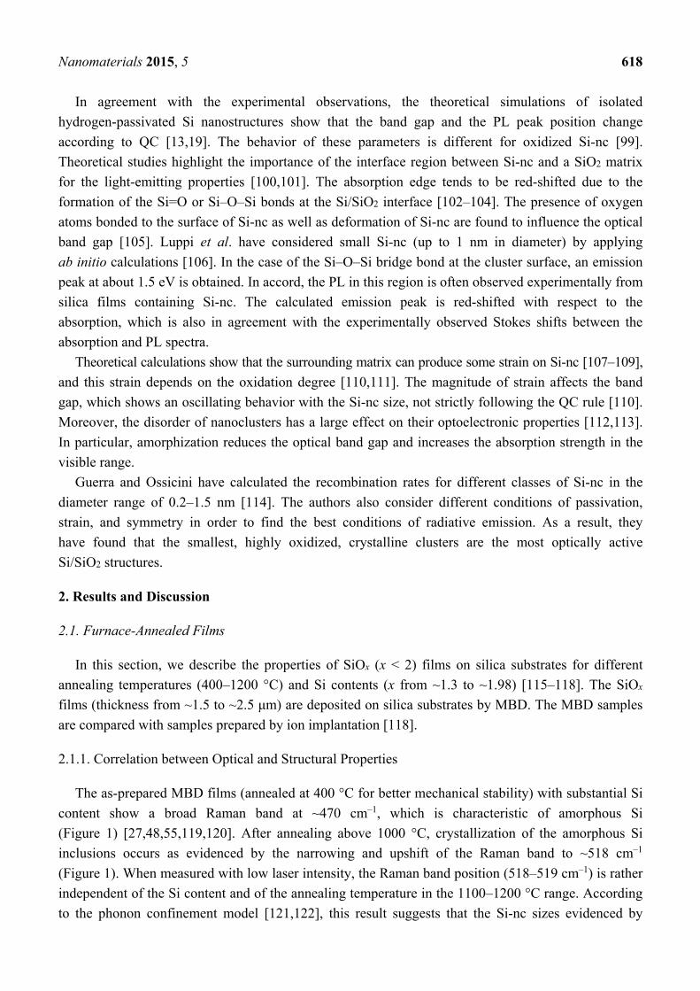
X-ray photoelectron spectroscopy (XPS) confirms that the structural reorganization is not complete
after furnace annealing (Figure 2). The Si–SiO2 phase separation increases with the annealing
temperature, which is evidenced by the increasing amount of elemental Si and SiO2 and the decreasing
amount of SiO. However, a large proportion of suboxides (10–15 at. % for x = 1.7) is still detected
after annealing at 1200 °C [116]. This result indicates incomplete Si–SiO2 phase separation in
these materials.
Figure 1. Raman spectra of a SiO1.75 film as-prepared and annealed at 1000 and 1200 °C
(fitted by two Gaussians). The spectra are vertically shifted for better presentation. The
Raman spectra are measured with laser intensity of ~103 W cm–2 at the sample.
Reproduced with permission from [116]. Copyright 2012, AIP Publishing LLC.
Nanomaterials 2015, 5 620
Figure 2. Composition of a SiO1.7 film provided by X-ray photoelectron spectroscopy
(XPS) as a function of the annealing temperature. Reproduced with permission from [116].
Copyright 2012, AIP Publishing LLC.
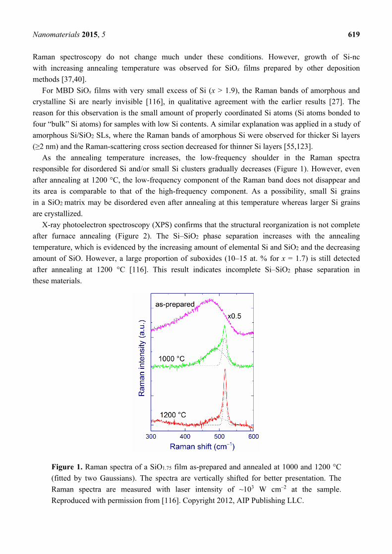
Figure 3. Band gap of SiOx films annealed at 1100 °C as a function of x. The inset shows
the band gap of a SiO1.4 film as a function of the annealing temperature. Reproduced with
permission from [116]. Copyright 2012, AIP Publishing LLC.
Additional information about the properties of SiOx films can be obtained from the band gap. For a
given annealing temperature (from 900 to 1200 °C), the band gap of SiOx films increases as the Si
content decreases [116]. For annealed at 1100 °C, the band gap increases from 2.2 to 2.6 eV as x
increases from 1.3 to 1.8 (Figure 3), meaning that the Si-nc sizes somewhat decrease. According to the
ab initio calculations for Si-nc with oxygen bonds at the Si/SiO2 interface, the obtained band gap
change (2.2–2.6 eV) corresponds only to a marginal change of the Si-nc sizes, the average size being
~1 nm [124]. On the other hand, the position of the maximum of the Raman bands at 518–519 cm–1
corresponds to larger sizes (3–4 nm) [121,122], and this value is supported by TEM measurements of
similar materials [125]. These different estimates can be connected with low sensitivity of the Raman
and TEM methods to very small Si grains. The low-frequency Raman scattering at 490–500 cm–1 can
be contributed by smaller Si-nc (1–2 nm) that may be partially disordered, which would agree with the
Si-nc sizes derived from the band gaps. It should also be mentioned that the band gap of Si clusters is a
complex function of a number of parameters in addition to the size, such as the crystallinity, strain due
Nanomaterials 2015, 5 621
to the SiO2 matrix, and degree of oxidation [110,112]. Moreover, the Tauc law is generally
applicable for amorphous semiconductors with absorption coefficients >104 cm–1 [88]. Thus, the
band gaps obtained by applying the Tauc law to crystalline Si grains with lower absorption may be
somewhat inaccurate.
The band gap of SiOx (x ~ 1.4 [116] and x ~ 1.8 [118]) films increases with the annealing
temperature (see the inset in Figure 3). This increase can be explained by amorphous-to-crystalline
transitions of Si clusters rather than by a decrease of their sizes, following the discussions by
Mirabella et al. [33]. Indeed, the Si-nc sizes should rather increase with the annealing
temperature [40,42] even though this increase for the MBD samples seems to be minor as suggested by
the Raman spectra.
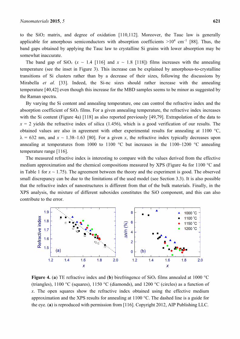
By varying the Si content and annealing temperature, one can control the refractive index and the
absorption coefficient of SiOx films. For a given annealing temperature, the refractive index increases
with the Si content (Figure 4a) [118] as also reported previously [49,79]. Extrapolation of the data to
x = 2 yields the refractive index of silica (1.456), which is a good verification of our results. The
obtained values are also in agreement with other experimental results for annealing at 1100 °C,
λ = 632 nm, and x ~ 1.38–1.63 [80]. For a given x, the refractive index typically decreases upon
annealing at temperatures from 1000 to 1100 °C but increases in the 1100–1200 °C annealing
temperature range [116].
The measured refractive index is interesting to compare with the values derived from the effective
medium approximation and the chemical compositions measured by XPS (Figure 4a for 1100 °C and
in Table 1 for x ~ 1.75). The agreement between the theory and the experiment is good. The observed
small discrepancy can be due to the limitations of the used model (see Section 3.3). It is also possible
that the refractive index of nanostructures is different from that of the bulk materials. Finally, in the
XPS analysis, the mixture of different suboxides constitutes the SiO component, and this can also
contribute to the error.
Figure 4. (a) TE refractive index and (b) birefringence of SiOx films annealed at 1000 °C
(triangles), 1100 °C (squares), 1150 °C (diamonds), and 1200 °C (circles) as a function of
x. The open squares show the refractive index obtained using the effective medium
approximation and the XPS results for annealing at 1100 °C. The dashed line is a guide for
the eye. (a) is reproduced with permission from [116]. Copyright 2012, AIP Publishing LLC.
Nanomaterials 2015, 5 622
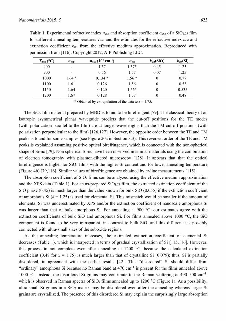
Table 1. Experimental refractive index nexp and absorption coefficient αexp of a SiO1.75 film
for different annealing temperatures Tann and the estimates for the refractive index nest and
extinction coefficient kest from the effective medium approximation. Reproduced with
permission from [116]. Copyright 2012, AIP Publishing LLC.
Tann (°C) nexp αexp (104 cm–1) nest kest(SiO) kest(Si)
400 - 1.57 1.575 0.45 1.25 900 - 0.56 1.57 0.07 1.25
1000 1.64 * 0.134 * 1.56 * 0 0.77 1100 1.61 0.126 1.56 0 0.53 1150 1.64 0.120 1.565 0 0.535 1200 1.67 0.128 1.57 0 0.48
* Obtained by extrapolation of the data to x = 1.75.
The SiOx film material prepared by MBD is found to be birefringent [79]. The classical theory of an
isotropic asymmetrical planar waveguide predicts that the cut-off positions for the TE modes
(with polarization parallel to the film) are at longer wavelengths than the TM cut-off positions (with
polarization perpendicular to the film) [126,127]. However, the opposite order between the TE and TM
peaks is found for some samples (see Figure 20a in Section 3.3). This reversed order of the TE and TM
peaks is explained assuming positive optical birefringence, which is connected with the non-spherical
shape of Si-nc [79]. Non spherical Si-nc have been observed in similar materials using the combination
of electron tomography with plasmon-filtered microscopy [128]. It appears that that the optical
birefringence is higher for SiOx films with the higher Si content and for lower annealing temperature
(Figure 4b) [79,116]. Similar values of birefringence are obtained by m-line measurements [115].
The absorption coefficient of SiOx films can be analyzed using the effective medium approximation
and the XPS data (Table 1). For an as-prepared SiO1.75 film, the extracted extinction coefficient of the
SiO phase (0.45) is much larger than the value known for bulk SiO (0.055) if the extinction coefficient
of amorphous Si (k = 1.25) is used for elemental Si. This mismatch would be smaller if the amount of
elemental Si was underestimated by XPS and/or the extinction coefficient of nanoscale amorphous Si
was larger than that of bulk amorphous Si. For annealing at 900 °C, our estimates agree with the
extinction coefficients of bulk SiO and amorphous Si. For films annealed above 1000 °C, the SiO
component is found to be very transparent, in contrast to bulk SiO, and this difference is possibly
connected with ultra-small sizes of the suboxide regions.
As the annealing temperature increases, the estimated extinction coefficient of elemental Si
decreases (Table 1), which is interpreted in terms of gradual crystallization of Si [115,116]. However,
this process in not complete even after annealing at 1200 °C, because the calculated extinction
coefficient (0.48 for x = 1.75) is much larger than that of crystalline Si (0.079); thus, Si is partially
disordered, in agreement with the earlier results [42]. This “disordered” Si should differ from
“ordinary” amorphous Si because no Raman band at 470 cm–1 is present for the films annealed above
1000 °C. Instead, the disordered Si grains may contribute to the Raman scattering at 490–500 cm–1,
which is observed in Raman spectra of SiOx films annealed up to 1200 °C (Figure 1). As a possibility,
ultra-small Si grains in a SiO2 matrix may be disordered even after the annealing whereas larger Si
grains are crystallized. The presence of this disordered Si may explain the surprisingly large absorption
Nanomaterials 2015, 5 623
of the annealed SiOx films. Moreover, the optical properties of bulk and nanoscale Si may differ, and
the absorption by SiO inclusions cannot be completely excluded. This explanation of the relatively
large absorption coefficient of annealed SiOx films is quite speculative, and additional experimental
data are required to draw more accurate conclusions.
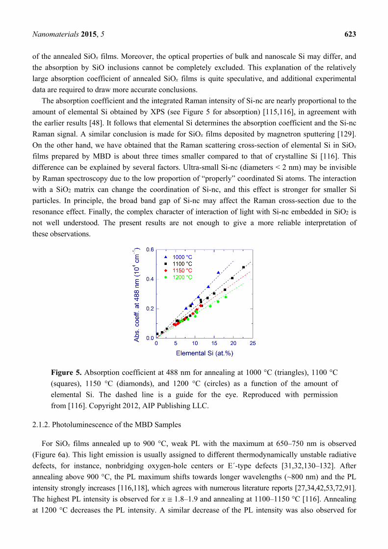
The absorption coefficient and the integrated Raman intensity of Si-nc are nearly proportional to the
amount of elemental Si obtained by XPS (see Figure 5 for absorption) [115,116], in agreement with
the earlier results [48]. It follows that elemental Si determines the absorption coefficient and the Si-nc
Raman signal. A similar conclusion is made for SiOx films deposited by magnetron sputtering [129].
On the other hand, we have obtained that the Raman scattering cross-section of elemental Si in SiOx
films prepared by MBD is about three times smaller compared to that of crystalline Si [116]. This
difference can be explained by several factors. Ultra-small Si-nc (diameters < 2 nm) may be invisible
by Raman spectroscopy due to the low proportion of “properly” coordinated Si atoms. The interaction
with a SiO2 matrix can change the coordination of Si-nc, and this effect is stronger for smaller Si
particles. In principle, the broad band gap of Si-nc may affect the Raman cross-section due to the
resonance effect. Finally, the complex character of interaction of light with Si-nc embedded in SiO2 is
not well understood. The present results are not enough to give a more reliable interpretation of
these observations.
Figure 5. Absorption coefficient at 488 nm for annealing at 1000 °C (triangles), 1100 °C
(squares), 1150 °C (diamonds), and 1200 °C (circles) as a function of the amount of
elemental Si. The dashed line is a guide for the eye. Reproduced with permission
from [116]. Copyright 2012, AIP Publishing LLC.
2.1.2. Photoluminescence of the MBD Samples
For SiOx films annealed up to 900 °C, weak PL with the maximum at 650–750 nm is observed
(Figure 6a). This light emission is usually assigned to different thermodynamically unstable radiative
defects, for instance, nonbridging oxygen-hole centers or E´-type defects [31,32,130–132]. After
annealing above 900 °C, the PL maximum shifts towards longer wavelengths (~800 nm) and the PL
intensity strongly increases [116,118], which agrees with numerous literature reports [27,34,42,53,72,91].
The highest PL intensity is observed for x ≅ 1.8–1.9 and annealing at 1100–1150 °C [116]. Annealing
at 1200 °C decreases the PL intensity. A similar decrease of the PL intensity was also observed for
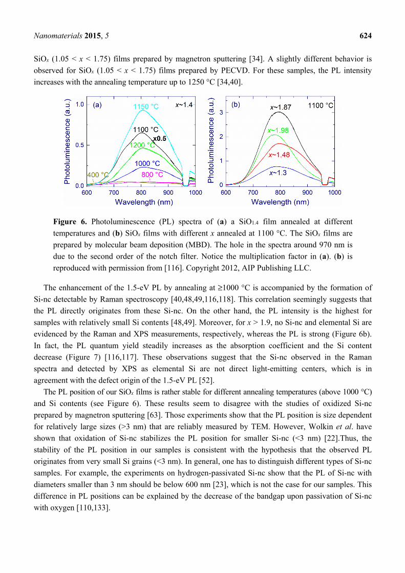
Nanomaterials 2015, 5 624
SiOx (1.05 < x < 1.75) films prepared by magnetron sputtering [34]. A slightly different behavior is
observed for SiOx (1.05 < x < 1.75) films prepared by PECVD. For these samples, the PL intensity
increases with the annealing temperature up to 1250 °C [34,40].
Figure 6. Photoluminescence (PL) spectra of (a) a SiO1.4 film annealed at different
temperatures and (b) SiOx films with different x annealed at 1100 °C. The SiOx films are
prepared by molecular beam deposition (MBD). The hole in the spectra around 970 nm is
due to the second order of the notch filter. Notice the multiplication factor in (a). (b) is
reproduced with permission from [116]. Copyright 2012, AIP Publishing LLC.
The enhancement of the 1.5-eV PL by annealing at ≥1000 °C is accompanied by the formation of
Si-nc detectable by Raman spectroscopy [40,48,49,116,118]. This correlation seemingly suggests that
the PL directly originates from these Si-nc. On the other hand, the PL intensity is the highest for
samples with relatively small Si contents [48,49]. Moreover, for x > 1.9, no Si-nc and elemental Si are
evidenced by the Raman and XPS measurements, respectively, whereas the PL is strong (Figure 6b).
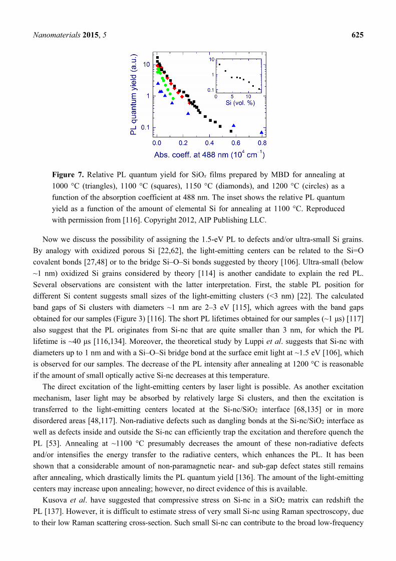
In fact, the PL quantum yield steadily increases as the absorption coefficient and the Si content
decrease (Figure 7) [116,117]. These observations suggest that the Si-nc observed in the Raman
spectra and detected by XPS as elemental Si are not direct light-emitting centers, which is in
agreement with the defect origin of the 1.5-eV PL [52].
The PL position of our SiOx films is rather stable for different annealing temperatures (above 1000 °C)
and Si contents (see Figure 6). These results seem to disagree with the studies of oxidized Si-nc
prepared by magnetron sputtering [63]. Those experiments show that the PL position is size dependent
for relatively large sizes (>3 nm) that are reliably measured by TEM. However, Wolkin et al. have
shown that oxidation of Si-nc stabilizes the PL position for smaller Si-nc (<3 nm) [22].Thus, the
stability of the PL position in our samples is consistent with the hypothesis that the observed PL
originates from very small Si grains (<3 nm). In general, one has to distinguish different types of Si-nc
samples. For example, the experiments on hydrogen-passivated Si-nc show that the PL of Si-nc with
diameters smaller than 3 nm should be below 600 nm [23], which is not the case for our samples. This
difference in PL positions can be explained by the decrease of the bandgap upon passivation of Si-nc
with oxygen [110,133].
Nanomaterials 2015, 5 625
Figure 7. Relative PL quantum yield for SiOx films prepared by MBD for annealing at
1000 °C (triangles), 1100 °C (squares), 1150 °C (diamonds), and 1200 °C (circles) as a
function of the absorption coefficient at 488 nm. The inset shows the relative PL quantum
yield as a function of the amount of elemental Si for annealing at 1100 °C. Reproduced
with permission from [116]. Copyright 2012, AIP Publishing LLC.
Now we discuss the possibility of assigning the 1.5-eV PL to defects and/or ultra-small Si grains.
By analogy with oxidized porous Si [22,62], the light-emitting centers can be related to the Si=O
covalent bonds [27,48] or to the bridge Si–O–Si bonds suggested by theory [106]. Ultra-small (below
~1 nm) oxidized Si grains considered by theory [114] is another candidate to explain the red PL.
Several observations are consistent with the latter interpretation. First, the stable PL position for
different Si content suggests small sizes of the light-emitting clusters (<3 nm) [22]. The calculated
band gaps of Si clusters with diameters ~1 nm are 2–3 eV [115], which agrees with the band gaps
obtained for our samples (Figure 3) [116]. The short PL lifetimes obtained for our samples (~1 μs) [117]
also suggest that the PL originates from Si-nc that are quite smaller than 3 nm, for which the PL
lifetime is ~40 μs [116,134]. Moreover, the theoretical study by Luppi et al. suggests that Si-nc with
diameters up to 1 nm and with a Si–O–Si bridge bond at the surface emit light at ~1.5 eV [106], which
is observed for our samples. The decrease of the PL intensity after annealing at 1200 °C is reasonable
if the amount of small optically active Si-nc decreases at this temperature.
The direct excitation of the light-emitting centers by laser light is possible. As another excitation
mechanism, laser light may be absorbed by relatively large Si clusters, and then the excitation is
transferred to the light-emitting centers located at the Si-nc/SiO2 interface [68,135] or in more
disordered areas [48,117]. Non-radiative defects such as dangling bonds at the Si-nc/SiO2 interface as
well as defects inside and outside the Si-nc can efficiently trap the excitation and therefore quench the
PL [53]. Annealing at ~1100 °C presumably decreases the amount of these non-radiative defects
and/or intensifies the energy transfer to the radiative centers, which enhances the PL. It has been
shown that a considerable amount of non-paramagnetic near- and sub-gap defect states still remains
after annealing, which drastically limits the PL quantum yield [136]. The amount of the light-emitting
centers may increase upon annealing; however, no direct evidence of this is available.
Kusova et al. have suggested that compressive stress on Si-nc in a SiO2 matrix can redshift the
PL [137]. However, it is difficult to estimate stress of very small Si-nc using Raman spectroscopy, due
to their low Raman scattering cross-section. Such small Si-nc can contribute to the broad low-frequency
Nanomaterials 2015, 5 626
shoulder at ~500 cm–1 (Figure 1). On the other hand, the Raman bands at 518–519 cm–1 observed in
our samples feature unstressed Si-nc with sizes of ~4 nm [121] that are also detected by TEM [125]. It
can be speculated that no substantial stress is exerted also on smaller Si-nc.
2.1.3. Comparison of the Implanted and MBD SiOx Samples (x ~ 1.8)
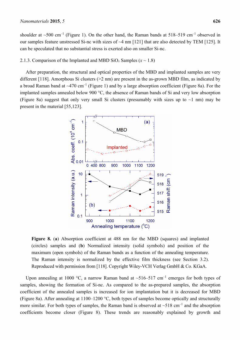
After preparation, the structural and optical properties of the MBD and implanted samples are very
different [118]. Amorphous Si clusters (>2 nm) are present in the as-grown MBD film, as indicated by
a broad Raman band at ~470 cm–1 (Figure 1) and by a large absorption coefficient (Figure 8a). For the
implanted samples annealed below 900 °C, the absence of Raman bands of Si and very low absorption
(Figure 8a) suggest that only very small Si clusters (presumably with sizes up to ~1 nm) may be
present in the material [55,123].
Figure 8. (a) Absorption coefficient at 488 nm for the MBD (squares) and implanted
(circles) samples and (b) Normalized intensity (solid symbols) and position of the
maximum (open symbols) of the Raman bands as a function of the annealing temperature.
The Raman intensity is normalized by the effective film thickness (see Section 3.2).
Reproduced with permission from [118]. Copyright Wiley-VCH Verlag GmbH & Co. KGaA.
Upon annealing at 1000 °C, a narrow Raman band at ~516–517 cm–1 emerges for both types of
samples, showing the formation of Si-nc. As compared to the as-prepared samples, the absorption
coefficient of the annealed samples is increased for ion implantation but it is decreased for MBD
(Figure 8a). After annealing at 1100–1200 °C, both types of samples become optically and structurally
more similar. For both types of samples, the Raman band is observed at ~518 cm–1 and the absorption
coefficients become closer (Figure 8). These trends are reasonably explained by growth and
Nanomaterials 2015, 5 627
crystallization of Si clusters in the implanted sample and by crystallization of amorphous clusters in
the MBD sample. Indeed, the extinction coefficient of crystalline Si is much smaller than that of
amorphous Si.
After annealing (>1000 °C), the normalized Raman intensity and the absorption coefficient are
larger for the MBD samples compared to the ion-implanted sample (Figure 8). This result indicates
that the amount of Si-nc with diameters of ≥2 nm is greater in the MBD films. This conclusion is also
supported by a smaller band gap for the MBD sample (~2.6 eV) compared to that for the implanted
sample (~3.3 eV). For both types of samples, a substantial amount of suboxides (~15%) is detected by
XPS even after annealing at 1200 °C, indicating that the Si–SiO2 phase separation is not complete.
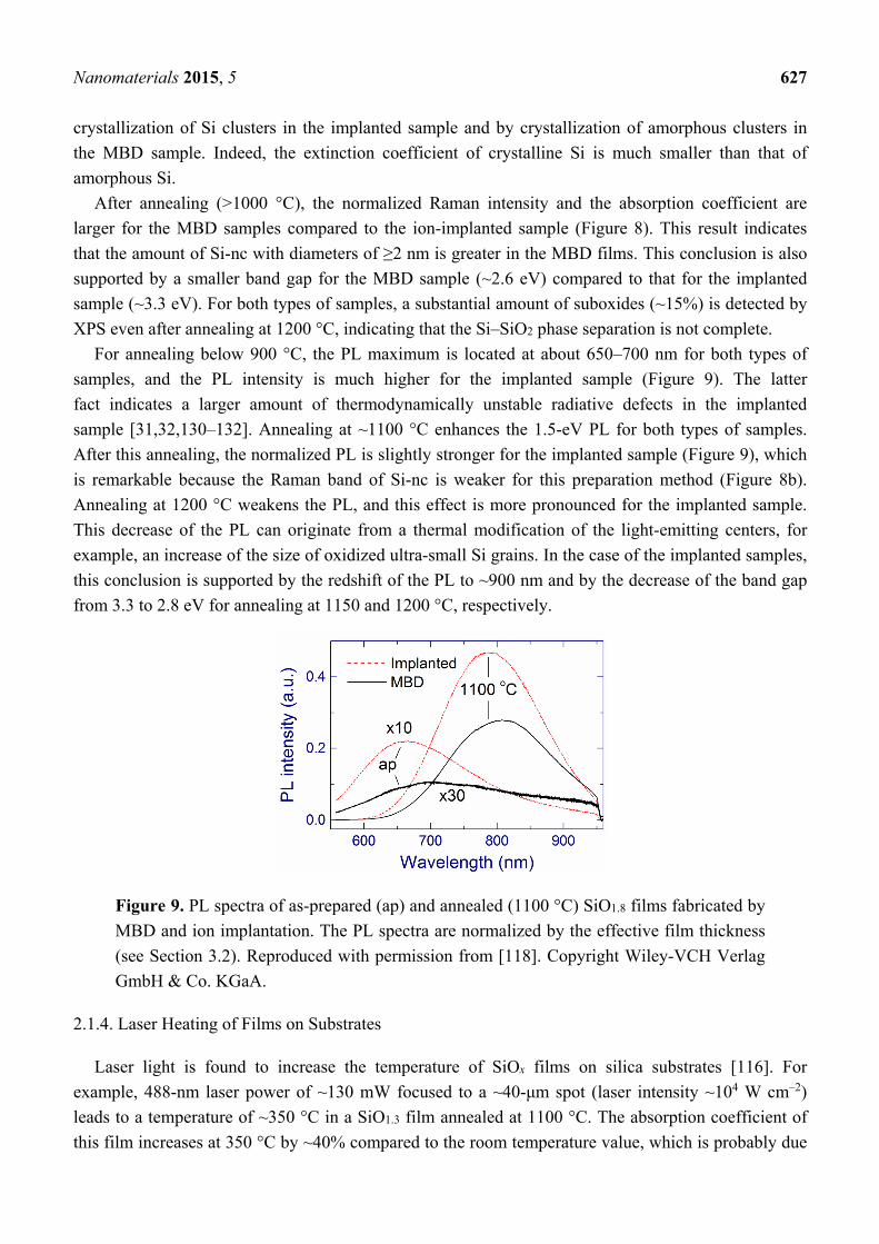
For annealing below 900 °C, the PL maximum is located at about 650–700 nm for both types of
samples, and the PL intensity is much higher for the implanted sample (Figure 9). The latter
fact indicates a larger amount of thermodynamically unstable radiative defects in the implanted
sample [31,32,130–132]. Annealing at ~1100 °C enhances the 1.5-eV PL for both types of samples.
After this annealing, the normalized PL is slightly stronger for the implanted sample (Figure 9), which
is remarkable because the Raman band of Si-nc is weaker for this preparation method (Figure 8b).
Annealing at 1200 °C weakens the PL, and this effect is more pronounced for the implanted sample.
This decrease of the PL can originate from a thermal modification of the light-emitting centers, for
example, an increase of the size of oxidized ultra-small Si grains. In the case of the implanted samples,
this conclusion is supported by the redshift of the PL to ~900 nm and by the decrease of the band gap
from 3.3 to 2.8 eV for annealing at 1150 and 1200 °C, respectively.
Figure 9. PL spectra of as-prepared (ap) and annealed (1100 °C) SiO1.8 films fabricated by
MBD and ion implantation. The PL spectra are normalized by the effective film thickness
(see Section 3.2). Reproduced with permission from [118]. Copyright Wiley-VCH Verlag
GmbH & Co. KGaA.
2.1.4. Laser Heating of Films on Substrates
Laser light is found to increase the temperature of SiOx films on silica substrates [116]. For
example, 488-nm laser power of ~130 mW focused to a ~40-μm spot (laser intensity ~104 W cm–2)
leads to a temperature of ~350 °C in a SiO1.3 film annealed at 1100 °C. The absorption coefficient of
this film increases at 350 °C by ~40% compared to the room temperature value, which is probably due
Nanomaterials 2015, 5 628
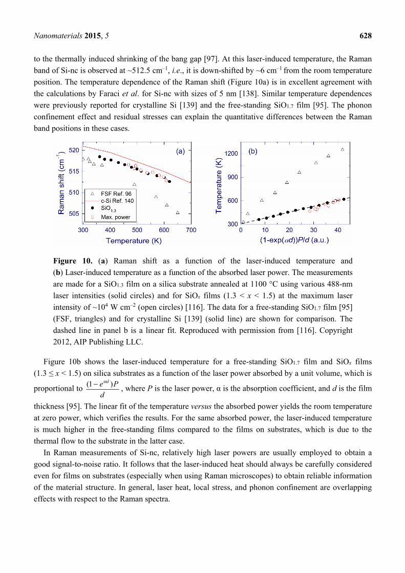
to the thermally induced shrinking of the bang gap [97]. At this laser-induced temperature, the Raman
band of Si-nc is observed at ~512.5 cm–1, i.e., it is down-shifted by ~6 cm–1 from the room temperature
position. The temperature dependence of the Raman shift (Figure 10a) is in excellent agreement with
the calculations by Faraci et al. for Si-nc with sizes of 5 nm [138]. Similar temperature dependences
were previously reported for crystalline Si [139] and the free-standing SiO1.7 film [95]. The phonon
confinement effect and residual stresses can explain the quantitative differences between the Raman
band positions in these cases.
Figure 10. (a) Raman shift as a function of the laser-induced temperature and
(b) Laser-induced temperature as a function of the absorbed laser power. The measurements
are made for a SiO1.3 film on a silica substrate annealed at 1100 °C using various 488-nm
laser intensities (solid circles) and for SiOx films (1.3 < x < 1.5) at the maximum laser
intensity of ~104 W cm–2 (open circles) [116]. The data for a free-standing SiO1.7 film [95]
(FSF, triangles) and for crystalline Si [139] (solid line) are shown for comparison. The
dashed line in panel b is a linear fit. Reproduced with permission from [116]. Copyright
2012, AIP Publishing LLC.
Figure 10b shows the laser-induced temperature for a free-standing SiO1.7 film and SiOx films
(1.3 ≤ x < 1.5) on silica substrates as a function of the laser power absorbed by a unit volume, which is
proportional to d
Pe d )1( α− , where P is the laser power, α is the absorption coefficient, and d is the film
thickness [95]. The linear fit of the temperature versus the absorbed power yields the room temperature
at zero power, which verifies the results. For the same absorbed power, the laser-induced temperature
is much higher in the free-standing films compared to the films on substrates, which is due to the
thermal flow to the substrate in the latter case.
In Raman measurements of Si-nc, relatively high laser powers are usually employed to obtain a
good signal-to-noise ratio. It follows that the laser-induced heat should always be carefully considered
even for films on substrates (especially when using Raman microscopes) to obtain reliable information
of the material structure. In general, laser heat, local stress, and phonon confinement are overlapping
effects with respect to the Raman spectra.
Nanomaterials 2015, 5 629
2.2. Laser Annealing of Free-Standing Films
2.2.1. Laser-Annealed Areas
We have studied CW laser annealing (488 nm) of free-standing SiOx films (0.5 and 2 μm-thick) and
Si/SiO2 SL (0.5-μm-thick). After preparation (Section 3.1), the free-standing films presumably contain
small Si-nc (up to 4 nm in diameter) [95,125]. The laser annealing is usually performed for ~1 s in air
atmosphere (if different is not stated). An optical photograph of a typical laser-annealed area on a
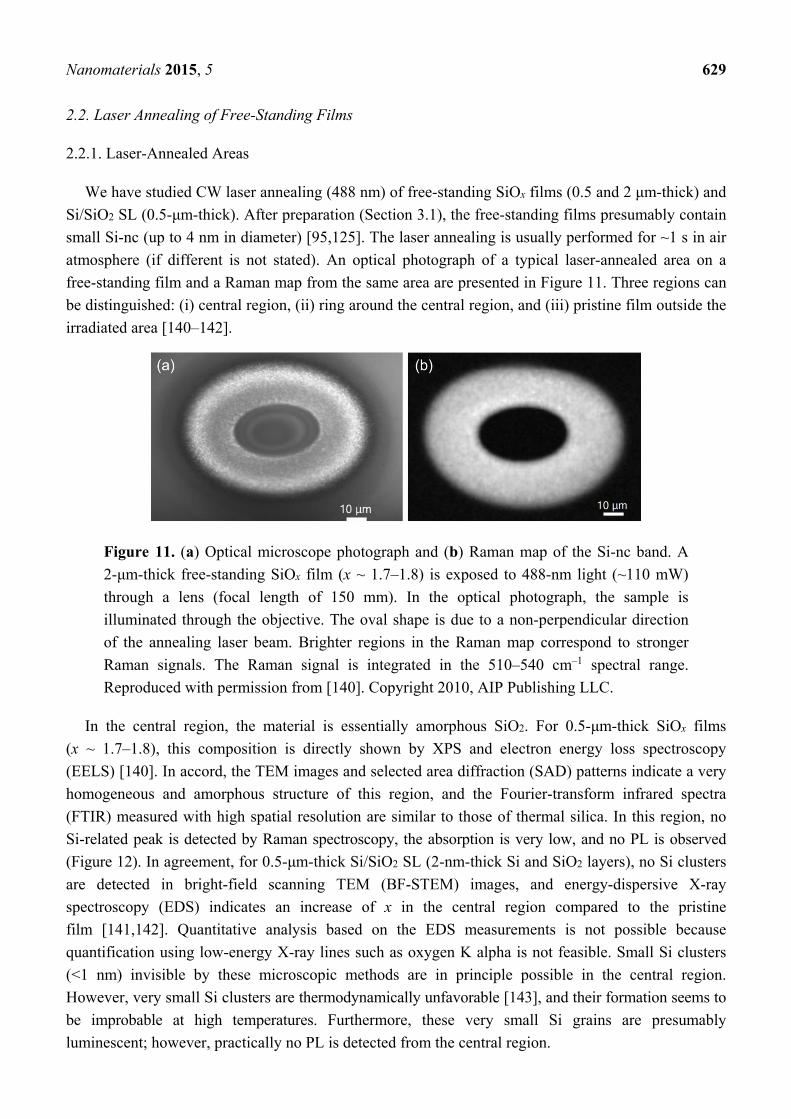
free-standing film and a Raman map from the same area are presented in Figure 11. Three regions can
be distinguished: (i) central region, (ii) ring around the central region, and (iii) pristine film outside the
irradiated area [140–142].
Figure 11. (a) Optical microscope photograph and (b) Raman map of the Si-nc band. A
2-μm-thick free-standing SiOx film (x ~ 1.7–1.8) is exposed to 488-nm light (~110 mW)
through a lens (focal length of 150 mm). In the optical photograph, the sample is
illuminated through the objective. The oval shape is due to a non-perpendicular direction
of the annealing laser beam. Brighter regions in the Raman map correspond to stronger
Raman signals. The Raman signal is integrated in the 510–540 cm–1 spectral range.
Reproduced with permission from [140]. Copyright 2010, AIP Publishing LLC.
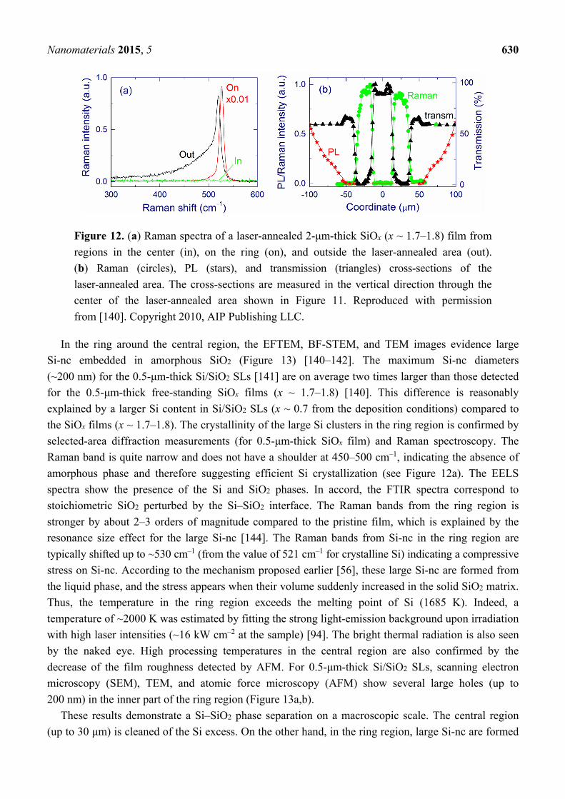
In the central region, the material is essentially amorphous SiO2. For 0.5-μm-thick SiOx films
(x ~ 1.7–1.8), this composition is directly shown by XPS and electron energy loss spectroscopy
(EELS) [140]. In accord, the TEM images and selected area diffraction (SAD) patterns indicate a very
homogeneous and amorphous structure of this region, and the Fourier-transform infrared spectra
(FTIR) measured with high spatial resolution are similar to those of thermal silica. In this region, no
Si-related peak is detected by Raman spectroscopy, the absorption is very low, and no PL is observed
(Figure 12). In agreement, for 0.5-μm-thick Si/SiO2 SL (2-nm-thick Si and SiO2 layers), no Si clusters
are detected in bright-field scanning TEM (BF-STEM) images, and energy-dispersive X-ray
spectroscopy (EDS) indicates an increase of x in the central region compared to the pristine
film [141,142]. Quantitative analysis based on the EDS measurements is not possible because
quantification using low-energy X-ray lines such as oxygen K alpha is not feasible. Small Si clusters
(<1 nm) invisible by these microscopic methods are in principle possible in the central region.
However, very small Si clusters are thermodynamically unfavorable [143], and their formation seems to
be improbable at high temperatures. Furthermore, these very small Si grains are presumably
luminescent; however, practically no PL is detected from the central region.
Nanomaterials 2015, 5 630
Figure 12. (a) Raman spectra of a laser-annealed 2-μm-thick SiOx (x ~ 1.7–1.8) film from
regions in the center (in), on the ring (on), and outside the laser-annealed area (out).
(b) Raman (circles), PL (stars), and transmission (triangles) cross-sections of the
laser-annealed area. The cross-sections are measured in the vertical direction through the
center of the laser-annealed area shown in Figure 11. Reproduced with permission
from [140]. Copyright 2010, AIP Publishing LLC.
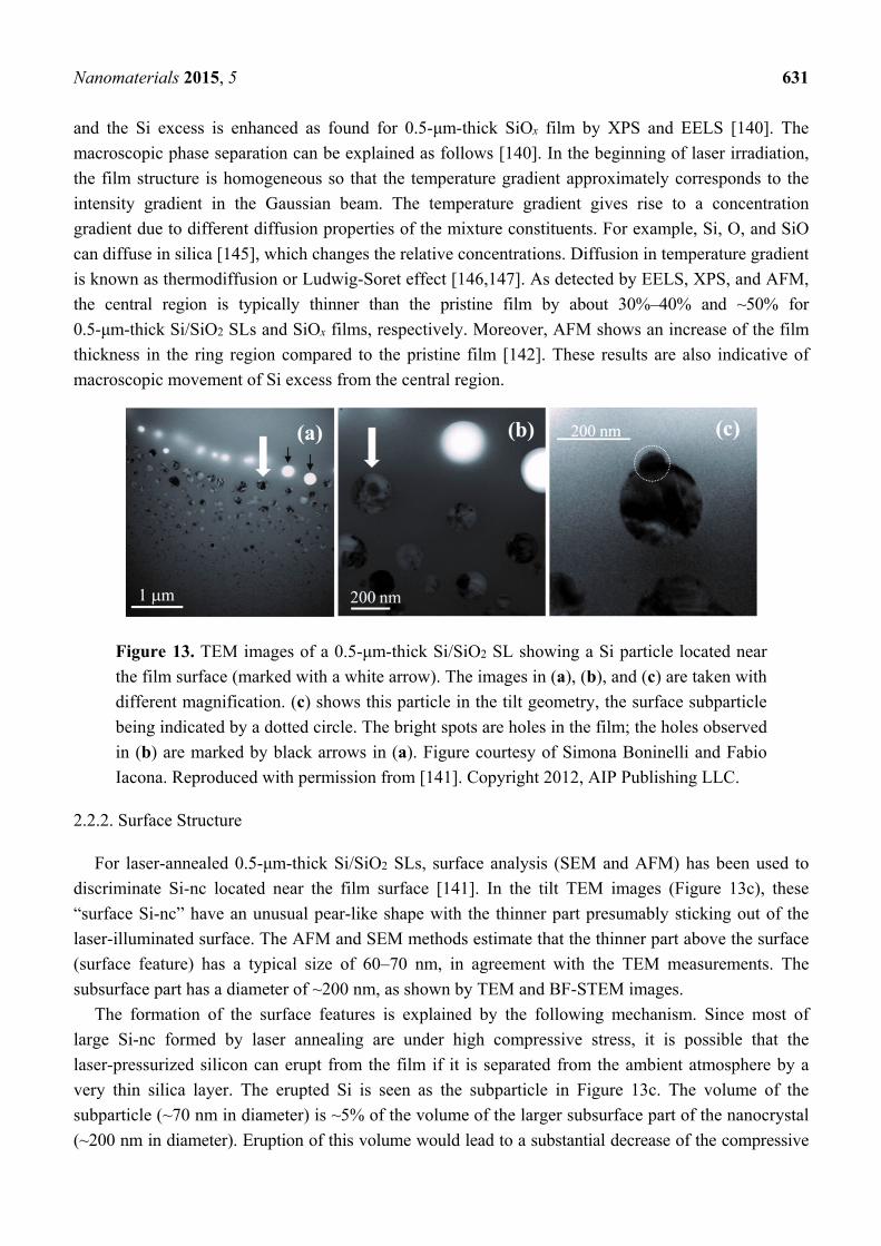
In the ring around the central region, the EFTEM, BF-STEM, and TEM images evidence large
Si-nc embedded in amorphous SiO2 (Figure 13) [140–142]. The maximum Si-nc diameters
(~200 nm) for the 0.5-μm-thick Si/SiO2 SLs [141] are on average two times larger than those detected
for the 0.5-μm-thick free-standing SiOx films (x ~ 1.7–1.8) [140]. This difference is reasonably
explained by a larger Si content in Si/SiO2 SLs (x ~ 0.7 from the deposition conditions) compared to
the SiOx films (x ~ 1.7–1.8). The crystallinity of the large Si clusters in the ring region is confirmed by
selected-area diffraction measurements (for 0.5-μm-thick SiOx film) and Raman spectroscopy. The
Raman band is quite narrow and does not have a shoulder at 450–500 cm–1, indicating the absence of
amorphous phase and therefore suggesting efficient Si crystallization (see Figure 12a). The EELS
spectra show the presence of the Si and SiO2 phases. In accord, the FTIR spectra correspond to
stoichiometric SiO2 perturbed by the Si–SiO2 interface. The Raman bands from the ring region is
stronger by about 2–3 orders of magnitude compared to the pristine film, which is explained by the
resonance size effect for the large Si-nc [144]. The Raman bands from Si-nc in the ring region are
typically shifted up to ~530 cm–1 (from the value of 521 cm–1 for crystalline Si) indicating a compressive
stress on Si-nc. According to the mechanism proposed earlier [56], these large Si-nc are formed from
the liquid phase, and the stress appears when their volume suddenly increased in the solid SiO2 matrix.
Thus, the temperature in the ring region exceeds the melting point of Si (1685 K). Indeed, a
temperature of ~2000 K was estimated by fitting the strong light-emission background upon irradiation
with high laser intensities (~16 kW cm–2 at the sample) [94]. The bright thermal radiation is also seen
by the naked eye. High processing temperatures in the central region are also confirmed by the
decrease of the film roughness detected by AFM. For 0.5-μm-thick Si/SiO2 SLs, scanning electron
microscopy (SEM), TEM, and atomic force microscopy (AFM) show several large holes (up to
200 nm) in the inner part of the ring region (Figure 13a,b).
These results demonstrate a Si–SiO2 phase separation on a macroscopic scale. The central region
(up to 30 μm) is cleaned of the Si excess. On the other hand, in the ring region, large Si-nc are formed
Nanomaterials 2015, 5 631
and the Si excess is enhanced as found for 0.5-μm-thick SiOx film by XPS and EELS [140]. The
macroscopic phase separation can be explained as follows [140]. In the beginning of laser irradiation,
the film structure is homogeneous so that the temperature gradient approximately corresponds to the
intensity gradient in the Gaussian beam. The temperature gradient gives rise to a concentration
gradient due to different diffusion properties of the mixture constituents. For example, Si, O, and SiO
can diffuse in silica [145], which changes the relative concentrations. Diffusion in temperature gradient
is known as thermodiffusion or Ludwig-Soret effect [146,147]. As detected by EELS, XPS, and AFM,
the central region is typically thinner than the pristine film by about 30%–40% and ~50% for
0.5-μm-thick Si/SiO2 SLs and SiOx films, respectively. Moreover, AFM shows an increase of the film
thickness in the ring region compared to the pristine film [142]. These results are also indicative of
macroscopic movement of Si excess from the central region.
Figure 13. TEM images of a 0.5-μm-thick Si/SiO2 SL showing a Si particle located near
the film surface (marked with a white arrow). The images in (a), (b), and (c) are taken with
different magnification. (c) shows this particle in the tilt geometry, the surface subparticle
being indicated by a dotted circle. The bright spots are holes in the film; the holes observed
in (b) are marked by black arrows in (a). Figure courtesy of Simona Boninelli and Fabio
Iacona. Reproduced with permission from [141]. Copyright 2012, AIP Publishing LLC.
2.2.2. Surface Structure
For laser-annealed 0.5-μm-thick Si/SiO2 SLs, surface analysis (SEM and AFM) has been used to
discriminate Si-nc located near the film surface [141]. In the tilt TEM images (Figure 13c), these
“surface Si-nc” have an unusual pear-like shape with the thinner part presumably sticking out of the
laser-illuminated surface. The AFM and SEM methods estimate that the thinner part above the surface
(surface feature) has a typical size of 60–70 nm, in agreement with the TEM measurements. The
subsurface part has a diameter of ~200 nm, as shown by TEM and BF-STEM images.
The formation of the surface features is explained by the following mechanism. Since most of
large Si-nc formed by laser annealing are under high compressive stress, it is possible that the
laser-pressurized silicon can erupt from the film if it is separated from the ambient atmosphere by a
very thin silica layer. The erupted Si is seen as the subparticle in Figure 13c. The volume of the
subparticle (~70 nm in diameter) is ~5% of the volume of the larger subsurface part of the nanocrystal
(~200 nm in diameter). Eruption of this volume would lead to a substantial decrease of the compressive
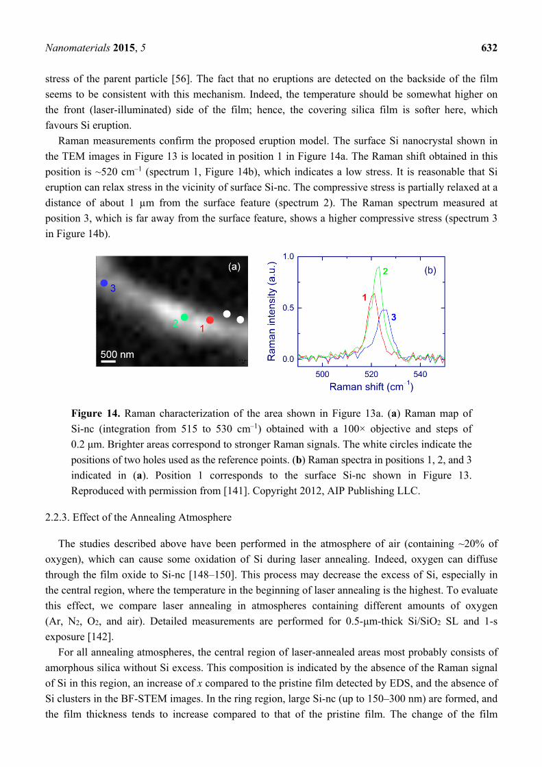
Nanomaterials 2015, 5 632
stress of the parent particle [56]. The fact that no eruptions are detected on the backside of the film
seems to be consistent with this mechanism. Indeed, the temperature should be somewhat higher on
the front (laser-illuminated) side of the film; hence, the covering silica film is softer here, which
favours Si eruption.
Raman measurements confirm the proposed eruption model. The surface Si nanocrystal shown in
the TEM images in Figure 13 is located in position 1 in Figure 14a. The Raman shift obtained in this
position is ~520 cm–1 (spectrum 1, Figure 14b), which indicates a low stress. It is reasonable that Si
eruption can relax stress in the vicinity of surface Si-nc. The compressive stress is partially relaxed at a
distance of about 1 µm from the surface feature (spectrum 2). The Raman spectrum measured at
position 3, which is far away from the surface feature, shows a higher compressive stress (spectrum 3
in Figure 14b).
Figure 14. Raman characterization of the area shown in Figure 13a. (a) Raman map of
Si-nc (integration from 515 to 530 cm–1) obtained with a 100× objective and steps of
0.2 μm. Brighter areas correspond to stronger Raman signals. The white circles indicate the
positions of two holes used as the reference points. (b) Raman spectra in positions 1, 2, and 3
indicated in (a). Position 1 corresponds to the surface Si-nc shown in Figure 13.
Reproduced with permission from [141]. Copyright 2012, AIP Publishing LLC.
2.2.3. Effect of the Annealing Atmosphere
The studies described above have been performed in the atmosphere of air (containing ~20% of
oxygen), which can cause some oxidation of Si during laser annealing. Indeed, oxygen can diffuse
through the film oxide to Si-nc [148–150]. This process may decrease the excess of Si, especially in
the central region, where the temperature in the beginning of laser annealing is the highest. To evaluate
this effect, we compare laser annealing in atmospheres containing different amounts of oxygen
(Ar, N2, O2, and air). Detailed measurements are performed for 0.5-μm-thick Si/SiO2 SL and 1-s
exposure [142].
For all annealing atmospheres, the central region of laser-annealed areas most probably consists of
amorphous silica without Si excess. This composition is indicated by the absence of the Raman signal
of Si in this region, an increase of x compared to the pristine film detected by EDS, and the absence of
Si clusters in the BF-STEM images. In the ring region, large Si-nc (up to 150–300 nm) are formed, and
the film thickness tends to increase compared to that of the pristine film. The change of the film
Nanomaterials 2015, 5 633
thickness was estimated using the AFM images taken from both sides of the film. These results support
the concept of macroscopic Si–SiO2 phase separation as a result of laser annealing.
The effect of oxygen can be analyzed by comparing the film thickness in the central region obtained
for different atmospheres. Indeed, two competitive processes, thermodiffusion and Si oxidation, affect
the film thickness in the opposite directions, tending, respectively, to decrease and to increase it. For
Ar atmospheres, the central region is thinner by ~150 nm than the pristine film, i.e., the thickness is
about 350 nm. This observation supports the concept of the macroscopic phase separation because Si
oxidation does not operate in the inert atmospheres. A similar change of the thickness occurs in air (the
thickness of the central region is 300–350 nm) also indicating minor Si oxidation.
In contrast, laser annealing in pure O2 increases the film thickness in the central region by
~20 nm compared to the pristine film. Thus, both thermodiffusion and Si oxidation seem to operate in
this case, practically compensating each other. It seems that a significant part of Si is oxidized upon
laser annealing in pure oxygen. The difference between the film thickness of the central region for
inert and O2 atmospheres is ~200 nm (larger in oxygen). 200 nm of SiO2 can be formed by oxidation of
about 100-nm Si layer, which corresponds to ~40% of all amount of elemental Si in the pristine SL
(125 2-nm-thick Si layer). According to the model suggested by Deal and Grove for crystalline Si,
1 bar of dry O2 at 1200 °C produces ~20-nm oxide film during 1 s, whereas a ~33-nm oxide is formed
for 100 s [149], which is in approximate agreement with our estimates. It should be reminded that the
temperature of laser annealing is sufficiently higher [94]. In addition, the extent of oxidation can differ
from these values because our pristine material is very different from crystalline Si.
The structure of the ring region is also affected by the amount of O2 in the ambient atmosphere. For
inert atmospheres, the AFM and BF-STEM images show that the ring region is very inhomogeneous. It
has areas with large Si-nc (up to 150 nm in diameter), with large non-spherical holes up to 300 nm, and
with smaller Si-nc (up to 50 nm in diameter). No surface Si-nc are observed in this case, as shown by
AFM and SEM. Raman spectroscopy indicates Si-nc with different stresses (Raman shifts from 518 to
530 cm–1) and regions with very different intensities of Raman bands of Si-nc. The BF-STEM images
show a “belt” of nano-channels (or pores) around the ring region. The size of these nano-channels can
be as low as several nanometers.
For laser annealing in air, the ring region contains Si-nc with diameters of up to 200 μm. A chain of
holes with sizes up to 200 μm is seen at the inner part of the ring of large Si-nc (Figure 15a). A number
of surface features are observed as discussed above.
For pure O2 atmosphere, in addition to Si-nc inside the film, SEM and AFM show a regular chain of
surface features that are located in the inner part of the ring at the front side of the film (Figure 15b).
The undersurface part of the surface Si-nc can be up to 300 nm in diameter. In agreement with the
suggested eruption model, Raman spectroscopy shows a relaxed stress for these surface Si-nc (Raman
shift of ~520 cm–1) whereas the Si-nc at the outer part are still under compressive stress (Raman shift
up to ~530 cm–1). No holes in the film are observed after laser annealing in O2 atmosphere.
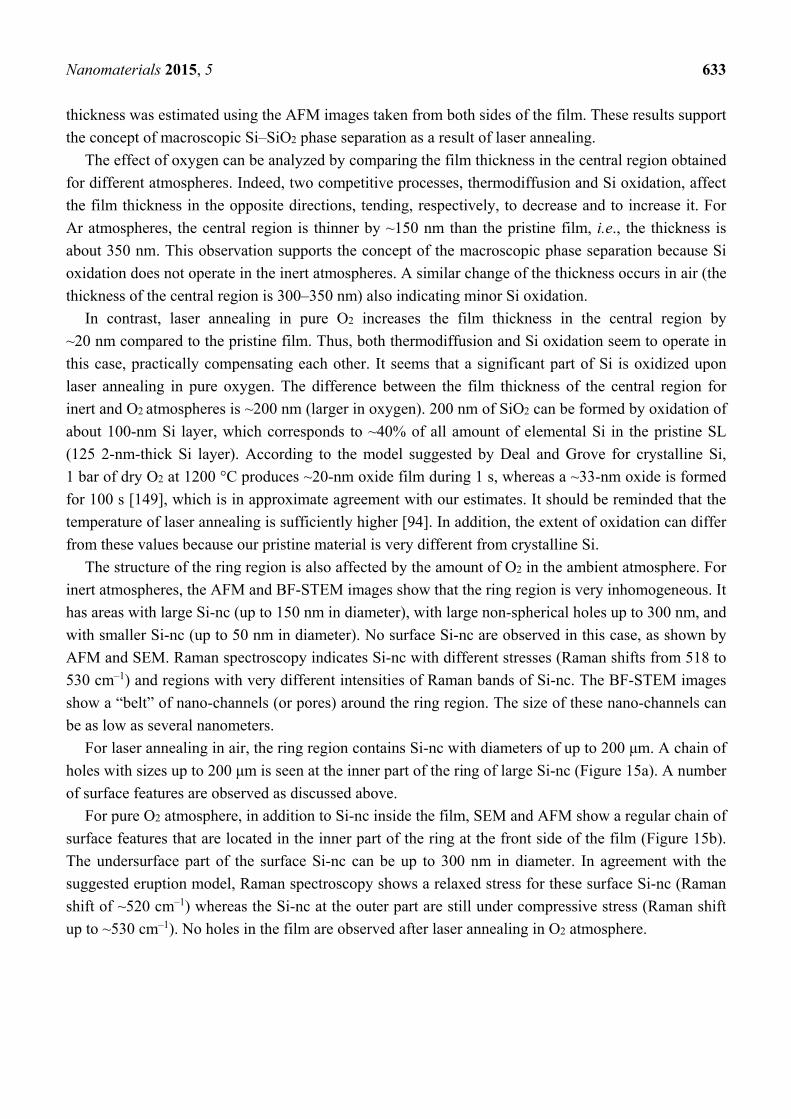
Nanomaterials 2015, 5 634
Figure 15. Secondary electron (SE) images of the front side of laser-annealed areas
produced in (a) air and (b) O2 atmospheres during 1-s exposure. Surface features are white,
holes are black. The scale is the same in both panels. Figure courtesy of Marianna Kemell.
Reprinted with permission from [142]. Copyright 2014, American Scientific Publishers.
Based on these results, it can be suggested that the holes produced in inert and air atmospheres are
formed via removal of surface Si-nc from the film. For laser annealing in air, the holes appear in the
positions where a chain of large surface Si-nc is observed in the case of O2 atmosphere (see Figure 15).
The laser-annealed areas with larger number of holes contain less surface Si-nc, and the presence of
oxygen increases the amount of surface Si-nc. This observation suggests that oxygen decreases the
removal of large Si-nc by the formation of a thin oxide layer covering surface Si-nc, which “glues”
them to the film. The large irregular holes obtained in the inert atmospheres also presumably originate
from large Si-nc removed from the film. The suggested mechanism of hole formation is consistent
with the dependence of the maximum Si-nc sizes on the annealing atmosphere. For inert atmospheres,
the largest Si-nc visible in the BF-STEM images are “only” ~150 nm in diameter because bigger Si-nc
are removed from the films forming holes with sizes of up to 300 nm. For O2 atmosphere, the largest
Si-nc (up to 300 nm) are detected because they are protected by thin oxide layers. Annealing in air
represents an intermediate case where the largest Si-nc are ~200 nm in diameter, and some Si-nc are
removed forming holes. In accord, with the proposed mechanism, holes are not observed in a
0.5-μm-thick SiOx film (x ~ 1.7–1.8) annealed in air [140]. For this film, Si-nc have diameters “only”
up to 100 nm, which are substantially smaller than the film thickness. These Si-nc are mostly located
below the film surface and, hence cannot be removed to form holes.
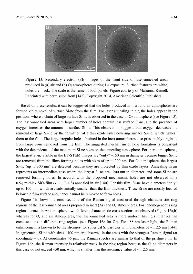
Figure 16 shows the cross-sections of the Raman signal measured through characteristic ring
regions of the laser-annealed areas prepared in inert (Ar) and O2 atmospheres. For inhomogeneous ring
regions formed in Ar atmosphere, two different characteristic cross-sections are observed (Figure 16a,b)
whereas for O2 and air atmospheres, the laser-annealed area is more uniform having similar Raman
cross-sections in different ring regions (see Figure 16c for O2). For 488-nm laser light, the Raman
enhancement is known to be the strongest for spherical Si particles with diameters of ~112.5 nm [144].
In agreement, Si-nc with sizes ~100 nm are observed in the areas with the strongest Raman signal (at
coordinate = 0). At coordinates >5 μm, the Raman spectra are similar to that of the pristine film. In
Figure 16b, the Raman intensity is relatively weak in the ring region because the Si-nc diameters in
this case do not exceed ~50 nm, which is smaller than the resonance value of ~112.5 nm.
Nanomaterials 2015, 5 635
For inert atmospheres (Figure 16a,b), the Raman signal is very weak at coordinates 2–3 μm. For air
and O2, this decrease of Raman intensity is less pronounced but still observable (Figure 16c). We call
this effect the secondary Si depletion, and it supports the model of macroscopic phase separation. We
tentatively explain the formation of this interval with low Raman intensity in the following way. When
the large Si-nc are formed in the ring region during laser annealing, the absorption coefficient in this
area strongly increases resulting in an increase of the temperature. Due to the thermal conductivity, the
temperature of the vicinity also increases, which leads to a temperature gradient and additional
macroscopic phase separation outside the ring region. This process seems to be more efficient for the
inert compared to oxygen-containing atmospheres. The position of this spatial interval roughly
coincides with the position of the belt of nano-pores and nano-channels observed by SEM in the inert
atmospheres. The exact mechanism of the formation of these pores is unclear.
Figure 16. Characteristic Raman cross-sections of the ring region. Two characteristic
cross-sections (a) and (b) are shown for Ar atmosphere, and the cross-sections (c) are
similar for O2. For air, the cross-sections are similar to the case of O2. The Raman signal is
integrated in the 230–585 cm–1 range. The data are normalized by the Raman intensity
measured from the pristine film. Reprinted with permission from [142]. Copyright 2014,
American Scientific Publishers.
2.2.4. Effect of the Exposure Period
Laser annealing with different exposures (10 ms and 100 s, in addition to 1 s) has been studied for
0.5-μm-thick Si/SiO2 SL mostly in air atmosphere [142]. For the central area, the results are similar for
all exposures: the EDS measurements show an increase of x (relative to the pristine film), no Raman
signal from Si-nc is detected, and no Si clusters are visible in the BF-STEM images. Thus, 10-ms
exposure is enough for the removal of excess Si from the central region. In other words, the formation
of the central region occurs in a millisecond time scale.
Nanomaterials 2015, 5 636
On the other hand, the ring region differs for different exposures. For 10-ms exposures, no holes
and surface features are found and Si-nc have diameters of up to 20–30 nm. For 1-s and 100-s laser
exposures, some holes and surface features are formed and Si-nc with diameters up to 200 and 250 nm,
respectively, are observed. Thus, longer laser exposure increases the Si-nc size. Coalescence of Si-nc
can be suggested for this process [73], because the number of Si-nc decreases for longer exposure
periods. The increase of the Si-nc sizes with the exposure period can probably explain the greater
amount of surface Si-nc observed for 100-s compared to 1-s exposure. For other atmospheres, the
prolonged laser annealing (100 s) also decreases the amount of small Si-nc and increases the average
sizes of Si-nc compared to 1-s exposure.
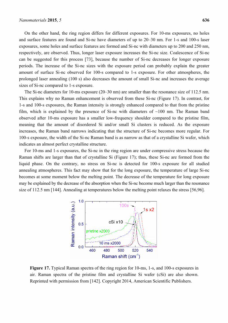
The Si-nc diameters for 10-ms exposure (20–30 nm) are smaller than the resonance size of 112.5 nm.
This explains why no Raman enhancement is observed from these Si-nc (Figure 17). In contrast, for
1-s and 100-s exposures, the Raman intensity is strongly enhanced compared to that from the pristine
film, which is explained by the presence of Si-nc with diameters of ~100 nm. The Raman band
observed after 10-ms exposure has a smaller low-frequency shoulder compared to the pristine film,
meaning that the amount of disordered Si and/or small Si clusters is reduced. As the exposure
increases, the Raman band narrows indicating that the structure of Si-nc becomes more regular. For
100-s exposure, the width of the Si-nc Raman band is as narrow as that of a crystalline Si wafer, which
indicates an almost perfect crystalline structure.
For 10-ms and 1-s exposures, the Si-nc in the ring region are under compressive stress because the
Raman shifts are larger than that of crystalline Si (Figure 17); thus, these Si-nc are formed from the
liquid phase. On the contrary, no stress on Si-nc is detected for 100-s exposure for all studied
annealing atmospheres. This fact may show that for the long exposure, the temperature of large Si-nc
becomes at some moment below the melting point. The decrease of the temperature for long exposure
may be explained by the decrease of the absorption when the Si-nc become much larger than the resonance
size of 112.5 nm [144]. Annealing at temperatures below the melting point relaxes the stress [56,96].
Figure 17. Typical Raman spectra of the ring region for 10-ms, 1-s, and 100-s exposures in
air. Raman spectra of the pristine film and crystalline Si wafer (cSi) are also shown.
Reprinted with permission from [142]. Copyright 2014, American Scientific Publishers.
Nanomaterials 2015, 5 637
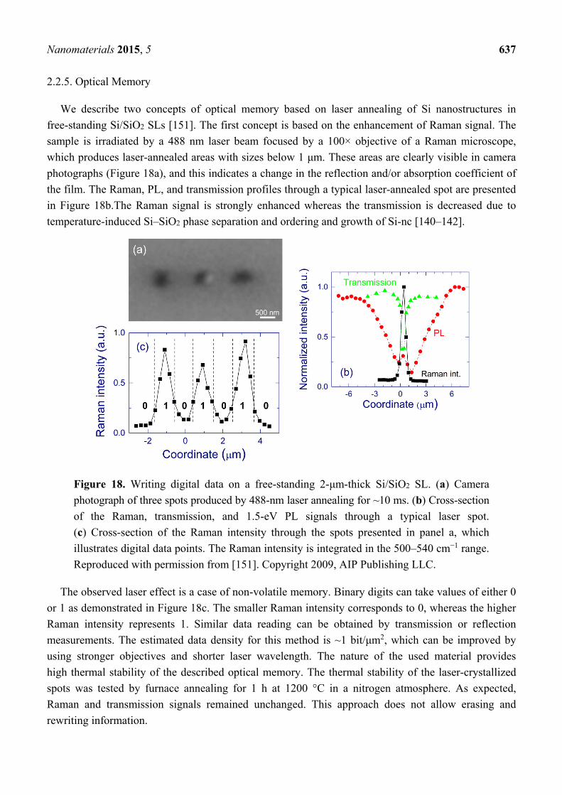
2.2.5. Optical Memory
We describe two concepts of optical memory based on laser annealing of Si nanostructures in
free-standing Si/SiO2 SLs [151]. The first concept is based on the enhancement of Raman signal. The
sample is irradiated by a 488 nm laser beam focused by a 100× objective of a Raman microscope,
which produces laser-annealed areas with sizes below 1 μm. These areas are clearly visible in camera
photographs (Figure 18a), and this indicates a change in the reflection and/or absorption coefficient of
the film. The Raman, PL, and transmission profiles through a typical laser-annealed spot are presented
in Figure 18b.The Raman signal is strongly enhanced whereas the transmission is decreased due to
temperature-induced Si–SiO2 phase separation and ordering and growth of Si-nc [140–142].
Figure 18. Writing digital data on a free-standing 2-μm-thick Si/SiO2 SL. (a) Camera
photograph of three spots produced by 488-nm laser annealing for ~10 ms. (b) Cross-section
of the Raman, transmission, and 1.5-eV PL signals through a typical laser spot.
(c) Cross-section of the Raman intensity through the spots presented in panel a, which
illustrates digital data points. The Raman intensity is integrated in the 500–540 cm−1 range.
Reproduced with permission from [151]. Copyright 2009, AIP Publishing LLC.
The observed laser effect is a case of non-volatile memory. Binary digits can take values of either 0
or 1 as demonstrated in Figure 18c. The smaller Raman intensity corresponds to 0, whereas the higher
Raman intensity represents 1. Similar data reading can be obtained by transmission or reflection
measurements. The estimated data density for this method is ~1 bit/μm2, which can be improved by
using stronger objectives and shorter laser wavelength. The nature of the used material provides
high thermal stability of the described optical memory. The thermal stability of the laser-crystallized
spots was tested by furnace annealing for 1 h at 1200 °C in a nitrogen atmosphere. As expected,
Raman and transmission signals remained unchanged. This approach does not allow erasing and
rewriting information.
Nanomaterials 2015, 5 638
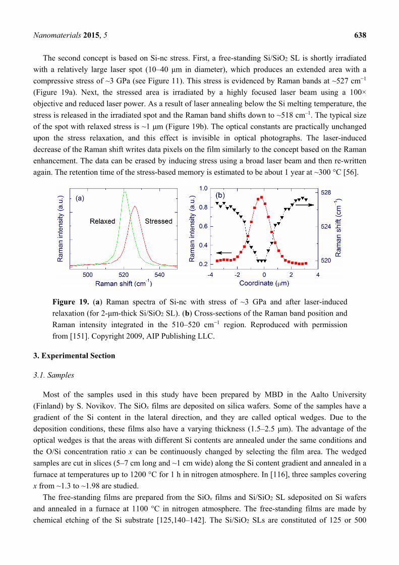
The second concept is based on Si-nc stress. First, a free-standing Si/SiO2 SL is shortly irradiated
with a relatively large laser spot (10–40 μm in diameter), which produces an extended area with a
compressive stress of ~3 GPa (see Figure 11). This stress is evidenced by Raman bands at ~527 cm−1
(Figure 19a). Next, the stressed area is irradiated by a highly focused laser beam using a 100×
objective and reduced laser power. As a result of laser annealing below the Si melting temperature, the
stress is released in the irradiated spot and the Raman band shifts down to ~518 cm–1. The typical size
of the spot with relaxed stress is ~1 μm (Figure 19b). The optical constants are practically unchanged
upon the stress relaxation, and this effect is invisible in optical photographs. The laser-induced
decrease of the Raman shift writes data pixels on the film similarly to the concept based on the Raman
enhancement. The data can be erased by inducing stress using a broad laser beam and then re-written
again. The retention time of the stress-based memory is estimated to be about 1 year at ~300 °C [56].
Figure 19. (a) Raman spectra of Si-nc with stress of ~3 GPa and after laser-induced
relaxation (for 2-μm-thick Si/SiO2 SL). (b) Cross-sections of the Raman band position and
Raman intensity integrated in the 510–520 cm−1 region. Reproduced with permission
from [151]. Copyright 2009, AIP Publishing LLC.
3. Experimental Section
3.1. Samples
Most of the samples used in this study have been prepared by MBD in the Aalto University
(Finland) by S. Novikov. The SiOx films are deposited on silica wafers. Some of the samples have a
gradient of the Si content in the lateral direction, and they are called optical wedges. Due to the
deposition conditions, these films also have a varying thickness (1.5–2.5 μm). The advantage of the
optical wedges is that the areas with different Si contents are annealed under the same conditions and
the O/Si concentration ratio x can be continuously changed by selecting the film area. The wedged
samples are cut in slices (5–7 cm long and ~1 cm wide) along the Si content gradient and annealed in a
furnace at temperatures up to 1200 °C for 1 h in nitrogen atmosphere. In [116], three samples covering
x from ~1.3 to ~1.98 are studied.
The free-standing films are prepared from the SiOx films and Si/SiO2 SL sdeposited on Si wafers
and annealed in a furnace at 1100 °C in nitrogen atmosphere. The free-standing films are made by
chemical etching of the Si substrate [125,140–142]. The Si/SiO2 SLs are constituted of 125 or 500
Nanomaterials 2015, 5 639
pairs of 2-nm-thick Si and SiO2 layers, yielding the total film thicknesses 0.5 or 2 μm, respectively.
The thicknesses of the free-standing SiOx films (x ~ 1.7–1.8) are 0.5 and 2 μm.
One sample is made by Si-ion implantation into a silica substrate in the Accelerator Laboratory
(University of Helsinki) [118]. The implantation of Si ions into a silica plate was done with different
energies (30, 56, 98, 160, 250, and 400 keV) and doses to achieve a nearly constant Si excess in the
SiOx layer with a thickness of ~750 nm. The O/Si concentration ratio x estimated by XPS is ~1.8. The
implanted sample is annealed at various temperatures up to 1200 °C for 1 h in a nitrogen atmosphere.
3.2. Equipment
The main analytical techniques used in our laboratory are Raman, PL, and UV-visible absorption
methods. Two setups have been used to record the Raman and PL spectra. The first setup consists of
an argon-ion laser (488 nm, Melles Griot 543-AP-A01), a spectrometer (Acton SpectraPro 500I), and a
charge-coupled device camera (Andor InstaSpec IV). The laser beam is focused with a lens to a spot
with a diameter of ~40 μm. The second setup allows us to perform micro-Raman and micro-PL
measurements. It consists of a confocal Raman microscope (LabRAM HR800, Horiba Jobin Yvon)
equipped with an argon-ion laser (488 nm). The size of the laser spot in the microscopic measurements
is down to ~1 μm. For both setups, the spectral resolution is ~2 cm−1 and 10 cm−1 for Raman and PL
measurements, respectively. The Raman bands of the films annealed at ≥1000 °C are fitted with two or
three Gaussians. The position of the Raman band of Si-nc is obtained from the position of the
higher-frequency Gaussian (~518–530 cm–1). The PL spectra are corrected for the spectral sensitivity of
the apparatus. The Raman and PL intensities are normalized by the effective thickness −d
ax dxe0
)2( and
−d
ax dxe0
)( , respectively, where the same absorption coefficients α is assumed for the laser and Raman
light, the absorption for the PL is neglected, and d is the film thickness [55].
Laser annealing of free-standing films is performed using a TEM00 beam of an argon-ion laser
(488 nm, power up to 110 mW at the sample) focused to spots with diameters ranging from ~1 to
~40 μm. The exposure time is mainly ~1 s, but 10-ms and 100-s exposures is also used in some
experiments. Most of laser-annealing studies are performed in air; however, a number of
measurements are done in O2, N2, and Ar atmospheres.
The absorption coefficient is obtained from the transmission and reflection spectra [152], recorded
with a fiber-optics spectrometer (SD2000, Ocean Optics) and a broadband light source (DH-2000, Top
Sensor Systems) or by measuring transmitted and reflected laser light using a power meter (NOVA II,
OPHIR). The micro-transmission measurements of the 488-nm light are carried out in the LabRAM
microscope with a large-area photodiode located behind the sample.
Additional measurements by other methods have been available from cooperation: XPS [115–118]
including measurements with high spatial resolution [140], FTIR spectroscopy with high spatial
resolution [140], TEM including bright-field scanning (BF), STEM and EFTEM [140,141],
EELS [140], SEM and EDS [141,142], AFM [141,142], and m-line measurements [115]. The
equipment used in these methods is described in the given references.
Nanomaterials 2015, 5 640
3.3. PL-Filtering Effect
The method to measure the optical properties of the films utilizes the PL-filtering effect. The PL
filtering is observed when the PL spectra are measured in a direction along the film surface. In this
case, narrow and polarized spectral peaks are detected (Figure 20a). The PL filtering has been
observed in various silica films containing Si-nc [49,57,59,79,85–87,94].
The PL-filtering effect can be interpreted in terms of delocalization of guided modes near the
cut-off frequency [49,57,79,85]. The minimal losses occur near the cut-off wavelengths, for which the
delocalized light travels mostly in the transparent substrate rather than in the absorbing film. Thus, the
narrow peaks seen in the PL spectra obtained in the waveguiding direction correspond to the cut-off
wavelengths. The mode localization is a function of the generalized frequency parameter written for an
asymmetrical planar waveguide in the form: = 2 ( − ) λ⁄ (1)
where and are the refractive indexes of the film and substrate, respectively, d is the film
thickness, and λ is the wavelength. This equation is obtained assuming weak-guiding
approximation ( − ) ≪ 1 [127]. For the cut-off condition = (2 + 1)π 2⁄ , Equation (1) yields
the cut-off wavelengths.
Figure 20b shows a typical transmission spectrum of an annealed SiO1.5 film on a silica substrate.
The spacing of the interference patterns (in cm–1) can be written as: = 1 2⁄ (2)
which provides the optical thickness (nd). The numerical information can be extracted from the
transmission spectrum by fitting it, for example, with the following empirical function: (λ) = + 1 − λ − 1 − sin λ + (3)
where T is the transmittance, and Pi are the fitting parameters [49]. In particular, the P5 parameter is
connected with the period of the oscillations, i.e., with the optical thickness. The TE refractive index is
relevant to transmission spectra. By using Equation (1) for the spacing between the TE peaks and
Equation (2), the TE refractive index and the film thickness can be extracted [85]. Next, the obtained
layer thickness together with the spacing between the TM peak positions is used to calculate the TM
refractive index. The obtained thickness is also used to calculate the absorption (extinction) coefficient
from the transmission and reflection measurements.
The model described above is called a simple model because it uses a few simplifications:
(i) Equation (1) corresponds to the weak-guiding approximation ( − ) ≪ 1; (ii) the procedure
uses only the interval between the cut-off peaks disregarding their actual positions; (iii) the material
dispersion is neglected; and (iv) a step-like profile is assumed for the refractive index.
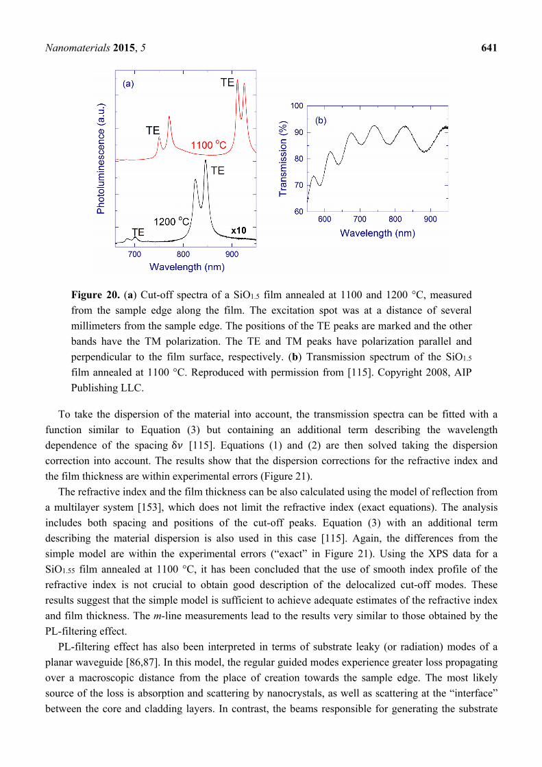
Nanomaterials 2015, 5 641
Figure 20. (a) Cut-off spectra of a SiO1.5 film annealed at 1100 and 1200 °C, measured
from the sample edge along the film. The excitation spot was at a distance of several
millimeters from the sample edge. The positions of the TE peaks are marked and the other
bands have the TM polarization. The TE and TM peaks have polarization parallel and
perpendicular to the film surface, respectively. (b) Transmission spectrum of the SiO1.5
film annealed at 1100 °C. Reproduced with permission from [115]. Copyright 2008, AIP
Publishing LLC.
To take the dispersion of the material into account, the transmission spectra can be fitted with a
function similar to Equation (3) but containing an additional term describing the wavelength
dependence of the spacing δ [115]. Equations (1) and (2) are then solved taking the dispersion
correction into account. The results show that the dispersion corrections for the refractive index and
the film thickness are within experimental errors (Figure 21).
The refractive index and the film thickness can be also calculated using the model of reflection from
a multilayer system [153], which does not limit the refractive index (exact equations). The analysis
includes both spacing and positions of the cut-off peaks. Equation (3) with an additional term
describing the material dispersion is also used in this case [115]. Again, the differences from the
simple model are within the experimental errors (“exact” in Figure 21). Using the XPS data for a
SiO1.55 film annealed at 1100 °C, it has been concluded that the use of smooth index profile of the
refractive index is not crucial to obtain good description of the delocalized cut-off modes. These
results suggest that the simple model is sufficient to achieve adequate estimates of the refractive index
and film thickness. The m-line measurements lead to the results very similar to those obtained by the
PL-filtering effect.
PL-filtering effect has also been interpreted in terms of substrate leaky (or radiation) modes of a
planar waveguide [86,87]. In this model, the regular guided modes experience greater loss propagating
over a macroscopic distance from the place of creation towards the sample edge. The most likely
source of the loss is absorption and scattering by nanocrystals, as well as scattering at the “interface”
between the core and cladding layers. In contrast, the beams responsible for generating the substrate
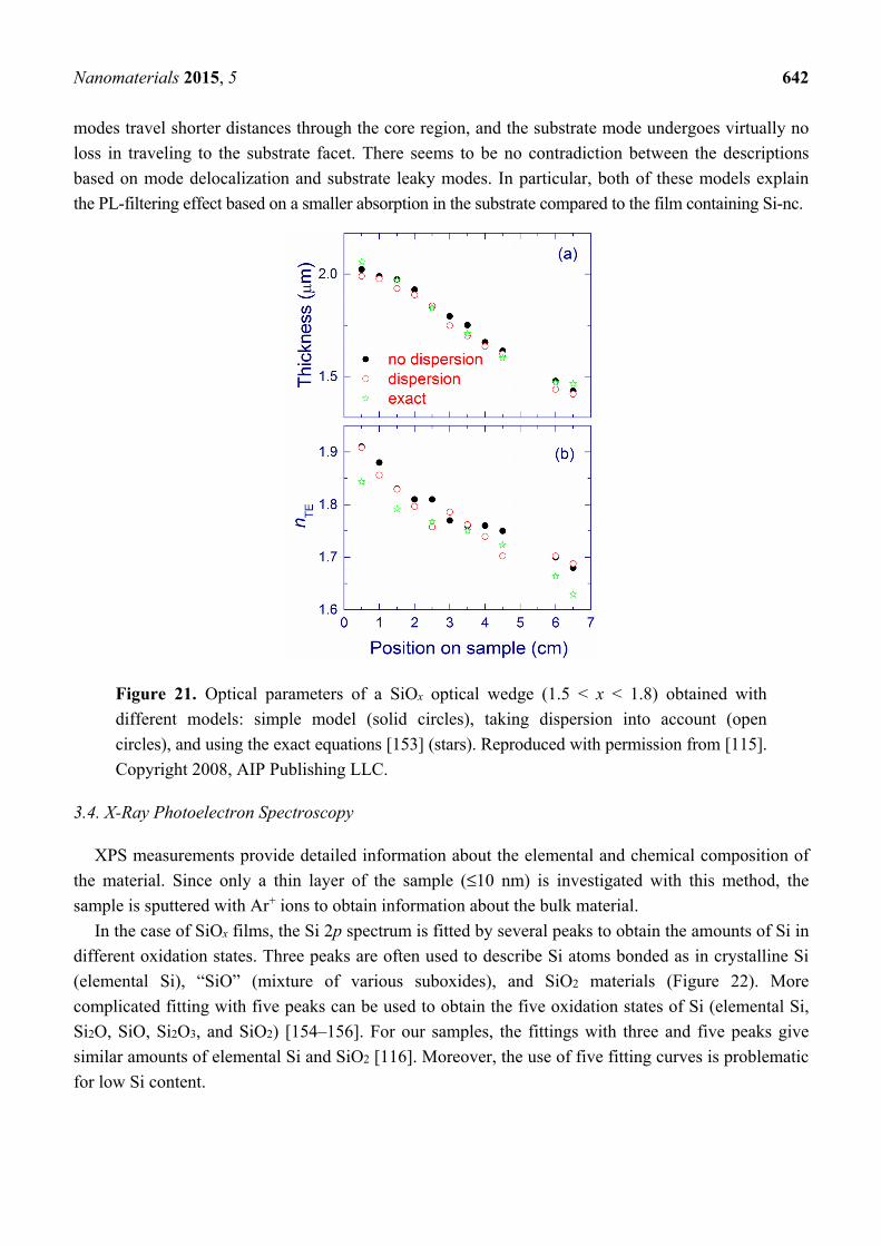
Nanomaterials 2015, 5 642
modes travel shorter distances through the core region, and the substrate mode undergoes virtually no
loss in traveling to the substrate facet. There seems to be no contradiction between the descriptions
based on mode delocalization and substrate leaky modes. In particular, both of these models explain
the PL-filtering effect based on a smaller absorption in the substrate compared to the film containing Si-nc.
Figure 21. Optical parameters of a SiOx optical wedge (1.5 < x < 1.8) obtained with
different models: simple model (solid circles), taking dispersion into account (open
circles), and using the exact equations [153] (stars). Reproduced with permission from [115].
Copyright 2008, AIP Publishing LLC.
3.4. X-Ray Photoelectron Spectroscopy
XPS measurements provide detailed information about the elemental and chemical composition of
the material. Since only a thin layer of the sample (≤10 nm) is investigated with this method, the
sample is sputtered with Ar+ ions to obtain information about the bulk material.
In the case of SiOx films, the Si 2p spectrum is fitted by several peaks to obtain the amounts of Si in
different oxidation states. Three peaks are often used to describe Si atoms bonded as in crystalline Si
(elemental Si), “SiO” (mixture of various suboxides), and SiO2 materials (Figure 22). More
complicated fitting with five peaks can be used to obtain the five oxidation states of Si (elemental Si,
Si2O, SiO, Si2O3, and SiO2) [154–156]. For our samples, the fittings with three and five peaks give
similar amounts of elemental Si and SiO2 [116]. Moreover, the use of five fitting curves is problematic
for low Si content.
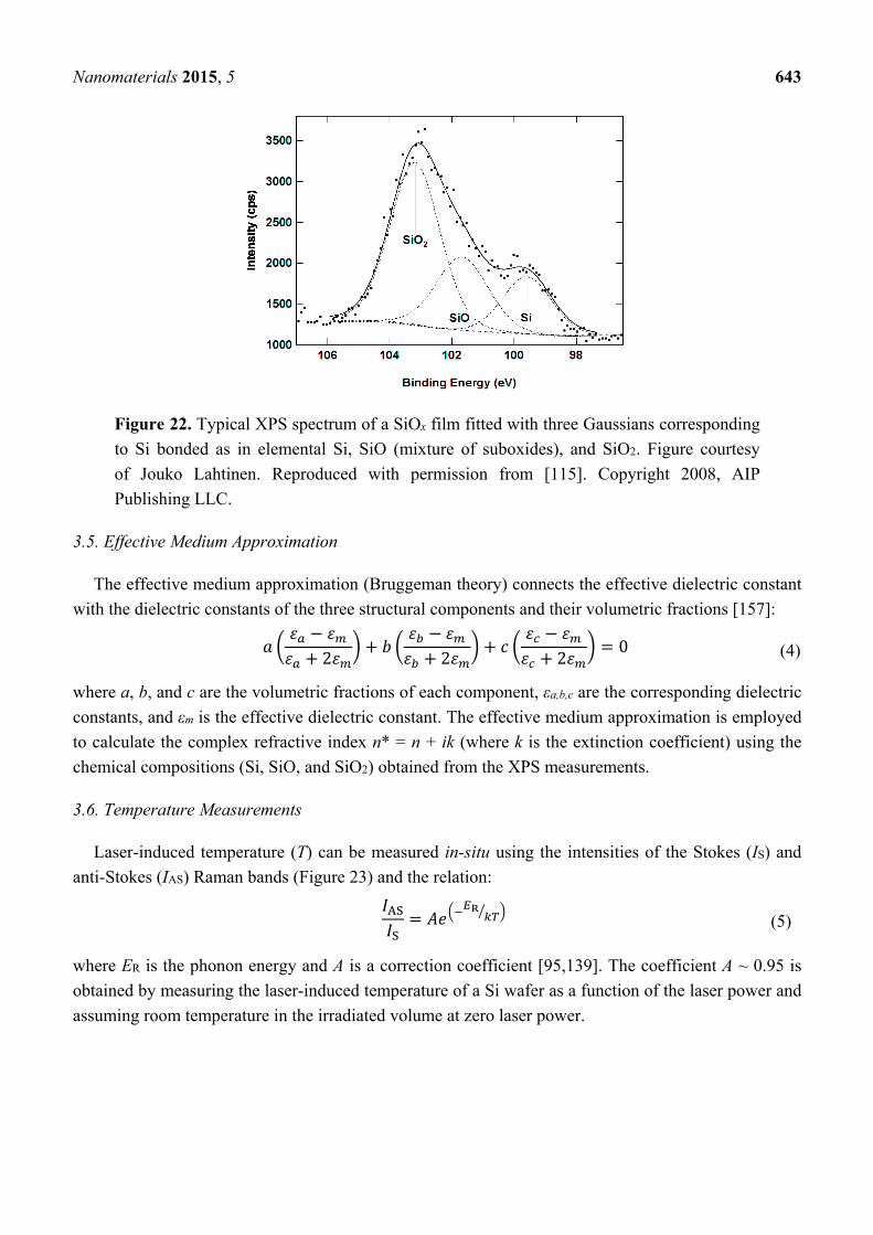
Nanomaterials 2015, 5 643
Figure 22. Typical XPS spectrum of a SiOx film fitted with three Gaussians corresponding
to Si bonded as in elemental Si, SiO (mixture of suboxides), and SiO2. Figure courtesy
of Jouko Lahtinen. Reproduced with permission from [115]. Copyright 2008, AIP
Publishing LLC.
3.5. Effective Medium Approximation
The effective medium approximation (Bruggeman theory) connects the effective dielectric constant
with the dielectric constants of the three structural components and their volumetric fractions [157]: −+ 2 + −+ 2 + −+ 2 = 0 (4)
where a, b, and c are the volumetric fractions of each component, εa,b,c are the corresponding dielectric
constants, and εm is the effective dielectric constant. The effective medium approximation is employed
to calculate the complex refractive index n* = n + ik (where k is the extinction coefficient) using the
chemical compositions (Si, SiO, and SiO2) obtained from the XPS measurements.
3.6. Temperature Measurements
Laser-induced temperature (T) can be measured in-situ using the intensities of the Stokes (IS) and
anti-Stokes (IAS) Raman bands (Figure 23) and the relation: = (5)
where ER is the phonon energy and A is a correction coefficient [95,139]. The coefficient A ~ 0.95 is
obtained by measuring the laser-induced temperature of a Si wafer as a function of the laser power and
assuming room temperature in the irradiated volume at zero laser power.
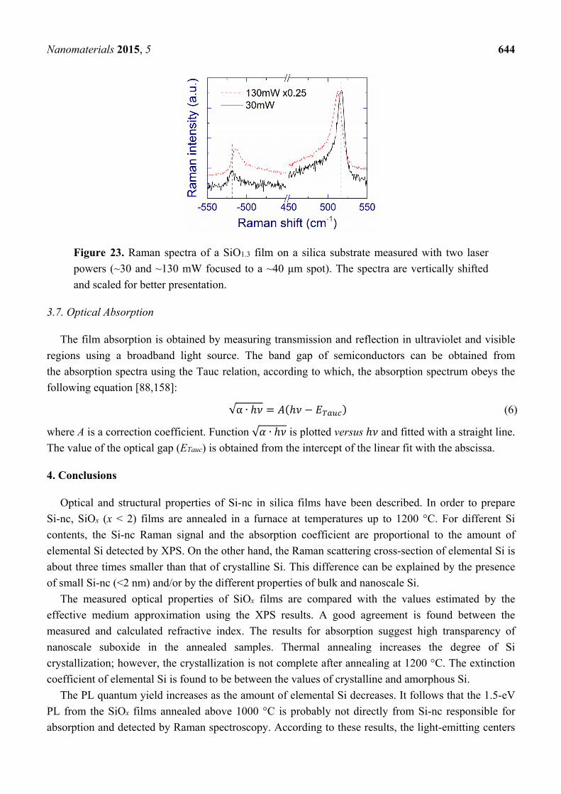
Nanomaterials 2015, 5 644
Figure 23. Raman spectra of a SiO1.3 film on a silica substrate measured with two laser
powers (~30 and ~130 mW focused to a ~40 μm spot). The spectra are vertically shifted
and scaled for better presentation.
3.7. Optical Absorption
The film absorption is obtained by measuring transmission and reflection in ultraviolet and visible
regions using a broadband light source. The band gap of semiconductors can be obtained from
the absorption spectra using the Tauc relation, according to which, the absorption spectrum obeys the
following equation [88,158]: √α ∙ ℎ = (ℎ − ) (6)
where A is a correction coefficient. Function √ ∙ ℎ is plotted versus ℎ and fitted with a straight line.
The value of the optical gap (ETauc) is obtained from the intercept of the linear fit with the abscissa.
4. Conclusions
Optical and structural properties of Si-nc in silica films have been described. In order to prepare
Si-nc, SiOx (x < 2) films are annealed in a furnace at temperatures up to 1200 °C. For different Si
contents, the Si-nc Raman signal and the absorption coefficient are proportional to the amount of
elemental Si detected by XPS. On the other hand, the Raman scattering cross-section of elemental Si is
about three times smaller than that of crystalline Si. This difference can be explained by the presence
of small Si-nc (<2 nm) and/or by the different properties of bulk and nanoscale Si.
The measured optical properties of SiOx films are compared with the values estimated by the
effective medium approximation using the XPS results. A good agreement is found between the
measured and calculated refractive index. The results for absorption suggest high transparency of
nanoscale suboxide in the annealed samples. Thermal annealing increases the degree of Si
crystallization; however, the crystallization is not complete after annealing at 1200 °C. The extinction
coefficient of elemental Si is found to be between the values of crystalline and amorphous Si.
The PL quantum yield increases as the amount of elemental Si decreases. It follows that the 1.5-eV
PL from the SiOx films annealed above 1000 °C is probably not directly from Si-nc responsible for
absorption and detected by Raman spectroscopy. According to these results, the light-emitting centers
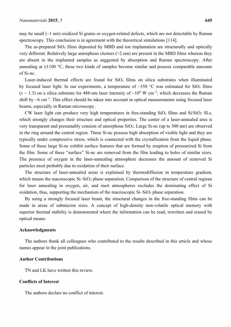
Nanomaterials 2015, 5 645
may be small (~1 nm) oxidized Si grains or oxygen-related defects, which are not detectable by Raman
spectroscopy. This conclusion is in agreement with the theoretical simulations [114].
The as-prepared SiOx films deposited by MBD and ion implantation are structurally and optically
very different. Relatively large amorphous clusters (>2 nm) are present in the MBD films whereas they
are absent in the implanted samples as suggested by absorption and Raman spectroscopy. After
annealing at ≥1100 °C, these two kinds of samples become similar and possess comparable amounts
of Si-nc.
Laser-induced thermal effects are found for SiOx films on silica substrates when illuminated
by focused laser light. In our experiments, a temperature of ~350 °C was estimated for SiOx films
(x ~ 1.3) on a silica substrate for 488-nm laser intensity of ~104 W cm–2, which decreases the Raman
shift by ~6 cm–1. This effect should be taken into account in optical measurements using focused laser
beams, especially in Raman microscopy.
CW laser light can produce very high temperatures in free-standing SiOx films and Si/SiO2 SLs,
which strongly changes their structure and optical properties. The center of a laser-annealed area is
very transparent and presumably consists of amorphous SiO2. Large Si-nc (up to 300 nm) are observed
in the ring around the central region. These Si-nc possess high absorption of visible light and they are
typically under compressive stress, which is connected with the crystallization from the liquid phase.
Some of these large Si-nc exhibit surface features that are formed by eruption of pressurized Si from
the film. Some of these “surface” Si-nc are removed from the film leading to holes of similar sizes.
The presence of oxygen in the laser-annealing atmosphere decreases the amount of removed Si
particles most probably due to oxidation of their surface.
The structure of laser-annealed areas is explained by thermodiffusion in temperature gradient,
which means the macroscopic Si–SiO2 phase separation. Comparison of the structure of central regions
for laser annealing in oxygen, air, and inert atmospheres excludes the dominating effect of Si
oxidation, thus, supporting the mechanism of the macroscopic Si–SiO2 phase separation.
By using a strongly focused laser beam, the structural changes in the free-standing films can be
made in areas of submicron sizes. A concept of high-density non-volatile optical memory with
superior thermal stability is demonstrated where the information can be read, rewritten and erased by
optical means.
Acknowledgments
The authors thank all colleagues who contributed to the results described in this article and whose
names appear in the joint publications.
Author Contributions
TN and LK have written this review.
Conflicts of Interest
The authors declare no conflict of interest.
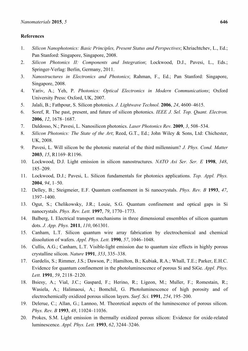
Nanomaterials 2015, 5 646
References
1. Silicon Nanophotonics: Basic Principles, Present Status and Perspectives; Khriachtchev, L., Ed.;
Pan Stanford: Singapore, Singapore, 2008.
2. Silicon Photonics II: Components and Integration; Lockwood, D.J., Pavesi, L., Eds.;
Springer-Verlag: Berlin, Germany, 2011.
3. Nanostructures in Electronics and Photonics; Rahman, F., Ed.; Pan Stanford: Singapore,
Singapore, 2008.
4. Yariv, A.; Yeh, P. Photonics: Optical Electronics in Modern Communications; Oxford
University Press: Oxford, UK, 2007.
5. Jalali, B.; Fathpour, S. Silicon photonics. J. Lightwave Technol. 2006, 24, 4600–4615.
6. Soref, R. The past, present, and future of silicon photonics. IEEE J. Sel. Top. Quant. Electron.
2006, 12, 1678–1687.
7. Daldosso, N.; Pavesi, L. Nanosilicon photonics. Laser Photonics Rev. 2009, 3, 508–534.
8. Silicon Photonics: The State of the Art; Reed, G.T., Ed.; John Wiley & Sons, Ltd: Chichester,
UK, 2008.
9. Pavesi, L. Will silicon be the photonic material of the third millennium? J. Phys. Cond. Matter
2003, 15, R1169–R1196.
10. Lockwood, D.J. Light emission in silicon nanostructures. NATO Asi Ser. Ser. E 1998, 348,
185–209.
11. Lockwood, D.J.; Pavesi, L. Silicon fundamentals for photonics applications. Top. Appl. Phys.
2004, 94, 1–50.
12. Delley, B.; Steigmeier, E.F. Quantum confinement in Si nanocrystals. Phys. Rev. B 1993, 47,
1397–1400.
13. Ogut, S.; Chelikowsky, J.R.; Louie, S.G. Quantum confinement and optical gaps in Si
nanocrystals. Phys. Rev. Lett. 1997, 79, 1770–1773.
14. Balberg, I. Electrical transport mechanisms in three dimensional ensembles of silicon quantum
dots. J. App. Phys. 2011, 110, 061301.
15. Canham, L.T. Silicon quantum wire array fabrication by electrochemical and chemical
dissolution of wafers. Appl. Phys. Lett. 1990, 57, 1046–1048.
16. Cullis, A.G.; Canham, L.T. Visible-light emission due to quantum size effects in highly porous
crystalline silicon. Nature 1991, 353, 335–338.
17. Gardelis, S.; Rimmer, J.S.; Dawson, P.; Hamilton, B.; Kubiak, R.A.; Whall, T.E.; Parker, E.H.C.
Evidence for quantum confinement in the photoluminescence of porous Si and SiGe. Appl. Phys.
Lett. 1991, 59, 2118–2120.
18. Bsiesy, A.; Vial, J.C.; Gaspard, F.; Herino, R.; Ligeon, M.; Muller, F.; Romestain, R.;
Wasiela, A.; Halimaoui, A.; Bomchil, G. Photoluminescence of high porosity and of
electrochemically oxidized porous silicon layers. Surf. Sci. 1991, 254, 195–200.
19. Delerue, C.; Allan, G.; Lannoo, M. Theoretical aspects of the luminescence of porous silicon.
Phys. Rev. B 1993, 48, 11024–11036.
20. Prokes, S.M. Light emission in thermally oxidized porous silicon: Evidence for oxide-related
luminescence. Appl. Phys. Lett. 1993, 62, 3244–3246.
Nanomaterials 2015, 5 647
21. Gole, J.L.; Dudel, F.P.; Grantier, D.; Dixon, D.A. Origin of porous silicon photoluminescence:
Evidence for a surface bound oxyhydride-like emitter. Phys. Rev. B 1997, 56, 2137–2153.
22. Wolkin, M.V.; Jorne, J.; Fauchet, P.M.; Allan, G.; Delerue, C. Electronic states and
luminescence in porous silicon quantum dots: The role of oxygen. Phys. Rev. Lett. 1999, 82,
197–200.
23. Ledoux, G.; Gong, J.; Huisken, F.; Guillois, O.; Reynaud, C. Photoluminescence of
size-separated silicon nanocrystals: Confirmation of quantum confinement. Appl. Phys. Lett.
2002, 80, 4834–4836.
24. Hannah, D.C.; Yang, J.H.; Podsiadlo, P.; Chan, M.K.Y.; Demortiere, A.; Gosztola, D.J.;
Prakapenka, V.B.; Schatz, G.C.; Kortshagen, U.; Schaller, R.D. On the origin of
photoluminescence in silicon nanocrystals: Pressure-dependent structural and optical studies.
Nano Lett. 2012, 12, 4200–4205.
25. Kim, T.Y.; Park, N.M.; Kim, K.H.; Sung, G.Y.; Ok, Y.W.; Seong, T.Y.; Choi, C.J. Quantum
confinement effect of silicon nanocrystals in situ grown in silicon nitride films. Appl. Phys. Lett.
2004, 85, 5355–5357.
26. Rezgui, B.; Sibai, A.; Nychyporuk, T.; Lemiti, M.; Bremond, G. Photoluminescence and optical
absorption properties of silicon quantum dots embedded in Si-rich silicon nitride matrices.
J. Lumin. 2009, 129, 1744–1746.
27. Khriachtchev, L.; Novikov, S.; Lahtinen, J. Thermal annealing of Si/SiO2 materials: Modification
of structural and photoluminescence emission properties. J. Appl. Phys. 2002, 92, 5856–5862.
28. Lu, Z.H.; Lockwood, D.J.; Baribeau, J.M. Quantum confinement and light emission in SiO2/Si
superlattices. Nature 1995, 378, 258–260.
29. Zhuravlev, K.S.; Gilinsky, A.M.; Kobitsky, A.Y. Mechanism of photoluminescence of Si
nanocrystals fabricated in a SiO2 matrix. Appl. Phys. Lett. 1998, 73, 2962–2964.
30. Dhara, S.; Lu, C.Y.; Nair, K.G.M.; Chen, K.H.; Chen, C.P.; Huang, Y.F.; David, C.; Chen, L.C.;
Raj, B. Mechanism of bright red emission in Si nanoclusters. Nanotechnology 2008, 19, 395401.
31. Garrido Fernandez, B.; Lopez, M.; Garcia, C.; Perez-Rodriguez, A.; Morante, J.R.; Bonafos, C.;
Carrada, M.; Claverie, A. Influence of average size and interface passivation on the spectral
emission of Si nanocrystals embedded in SiO2. J. Appl. Phys. 2002, 91, 798–807.
32. Guha, S. Characterization of Si+ ion-implanted SiO2 films and silica glasses. J. Appl. Phys. 1998,
84, 5210–5217.
33. Mirabella, S.; Agosta, R.; Franzo, G.; Crupi, I.; Miritello, M.; Lo Savio, R.; Di Stefano, M.A.;
Di Marco, S.; Simone, F.; Terrasi, A. Light absorption in silicon quantum dots embedded in
silica. J. Appl. Phys. 2009, 106, 103505.
34. Franzo, G.; Miritello, M.; Boninelli, S.; Lo Savio, R.; Grimaldi, M.G.; Priolo, F.; Iacona, F.;
Nicotra, G.; Spinella, C.; Coffa, S. Microstructural evolution of SiOx films and its effect on the
luminescence of Si nanoclusters. J. Appl. Phys. 2008, 104, 094306.
35. Ternon, C.; Dufour, C.; Gourbilleau, F.; Rizk, R. Roles of interfaces in nanostructured silicon
luminescence. Eur. Phys. J. B 2004, 41, 325–332.
36. Alonso, M.I.; Marcus, I.C.; Garriga, M.; Goñi, A.R.; Jedrzejewski, J.; Balberg, I. Evidence of
quantum confinement effects on interband optical transitions in Si nanocrystals. Phys. Rev. B
2010, 82, 045302.
Nanomaterials 2015, 5 648
37. Roussel, M.; Talbot, E.; Pareige, P.; Gourbilleau, F. Influence of the supersaturation on Si
diffusion and growth of Si nanoparticles in silicon-rich silica. J. Appl. Phys. 2013, 113, 063519.
38. Antonova, I.V.; Gulyaev, M.; Savir, E.; Jedrzejewski, J.; Balberg, I. Charge storage,
photoluminescence, and cluster statistics in ensembles of Si quantum dots. Phys. Rev. B 2008,
77, 125318.
39. Balberg, I.; Savir, E.; Jedrzejewski, J.; Nassiopoulou, A.G.; Gardelis, S. Fundamental transport
processes in ensembles of silicon quantum dots. Phys. Rev. B 2007, 75, 235329.
40. Iacona, F.; Franzo, G.; Spinella, C. Correlation between luminescence and structural properties of
Si nanocrystals. J. Appl. Phys. 2000, 87, 1295–1303.
41. Trwoga, P.F.; Kenyon, A.J.; Pitt, C.W. Modeling the contribution of quantum confinement to
luminescence from silicon nanoclusters. J. Appl. Phys. 1998, 83, 3789–3794.
42. Boninelli, S.; Iacona, F.; Franzo, G.; Bongiorno, C.; Spinella, C.; Priolo, F. Formation, evolution
and photoluminescence properties of Si nanoclusters. J. Phys.: Condens. Matter 2007, 19, 225003.
43. Nassiopoulou, A.G. Encyclopedia of Nanoscience and Nanotechnology; Nalwa, H.S., Ed.;
American Scientific: Valencia, Spain, 2004; Volume 9, pp. 793–813.
44. Gardelis, S.; Nassiopoulou, A.G.; Manousiadis, P.; Milita, S.; Gkanatsiou, A.; Frangis, N.;
Lioutas, C.B. Structural and optical characterization of two-dimensional arrays of Si nanocrystals
embedded in SiO2 for photovoltaic applications. J. Appl. Phys. 2012, 111, 083536.
45. Gardelis, S.; Nassiopoulou, A.G.; Vouroutzis, N.; Frangis, N. Effect of exciton migration on the
light emission properties in silicon nanocrystal ensembles. J. Appl. Phys. 2009, 105, 113509.
46. Hiller, D.; Goetze, S.; Munnik, F.; Jivanescu, M.; Gerlach, J.W.; Vogt, J.; Pippel, E.;
Zakharov, N.; Stesmans, A.; Zacharias, M. Nitrogen at the Si-nanocrystal/SiO2 interface and its
influence on luminescence and interface defects. Phys. Rev. B 2010, 82, 195401.
47. Seguini, G.; Castro, C.; Schamm-Chardon, S.; BenAssayag, G.; Pellegrino, P.; Perego, M.
Scaling size of the interplay between quantum confinement and surface related effects in
nanostructured silicon. Appl. Phys. Lett. 2013, 103, 023103.
48. Khriachtchev, L.; Räsänen, M.; Novikov, S.; Pavesi, L. Systematic correlation between Raman
spectra, photoluminescence intensity, and absorption coefficient of silica layers containing Si
nanocrystals. Appl. Phys. Lett. 2004, 85, 1511–1513.
49. Khriachtchev, L.; Räsänen, M.; Novikov, S.; Lahtinen, J. Tunable wavelength-selective
waveguiding of photoluminescence in Si-rich silica optical wedges. J. Appl. Phys. 2004, 95,
7592–7601.
50. Zacharias, M.; Blasing, J.; Veit, P.; Tsybeskov, L.; Hirschman, K.; Fauchet, P.M. Thermal
crystallization of amorphous Si/SiO2 superlattices. Appl. Phys. Lett. 1999, 74, 2614–2616.
51. Zacharias, M.; Heitmann, J.; Scholz, R.; Kahler, U.; Schmidt, M.; Blasing, J. Size-controlled
highly luminescent silicon nanocrystals: A SiO/SiO2 superlattice approach. Appl. Phys. Lett.
2002, 80, 661–663.
52. Godefroo, S.; Hayne, M.; Jivanescu, M.; Stesmans, A.; Zacharias, M.; Lebedev, O.I.;
van Tendeloo, G.; Moshchalkov, V.V. Classification and control of the origin of
photoluminescence from Si nanocrystals. Nat. Nanotechnol. 2008, 3, 174–178.
53. Hiller, D.; Jivanescu, M.; Stesmans, A.; Zacharias, M. P-b(0) centers at the Si-nanocrystal/SiO2
interface as the dominant photoluminescence quenching defect. J. Appl. Phys. 2010, 107, 084309.
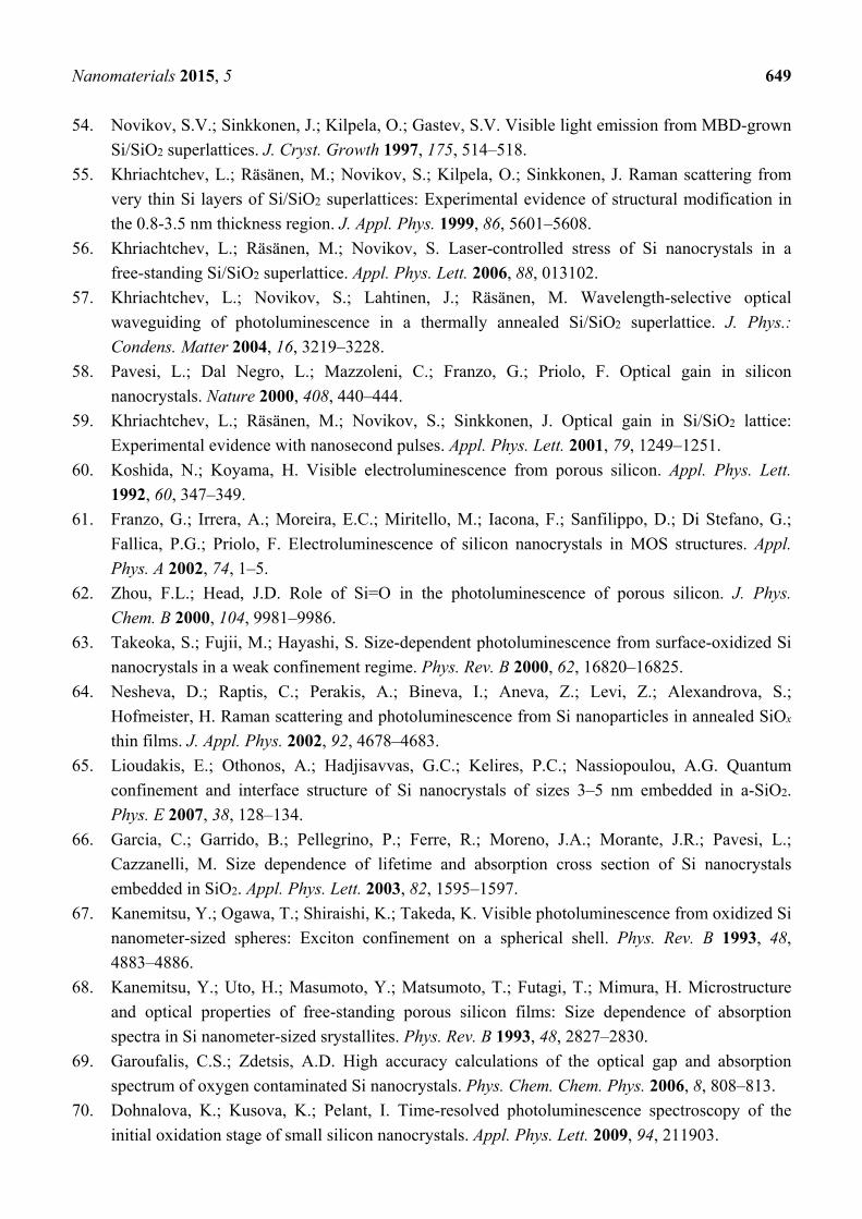
Nanomaterials 2015, 5 649
54. Novikov, S.V.; Sinkkonen, J.; Kilpela, O.; Gastev, S.V. Visible light emission from MBD-grown
Si/SiO2 superlattices. J. Cryst. Growth 1997, 175, 514–518.
55. Khriachtchev, L.; Räsänen, M.; Novikov, S.; Kilpela, O.; Sinkkonen, J. Raman scattering from
very thin Si layers of Si/SiO2 superlattices: Experimental evidence of structural modification in
the 0.8-3.5 nm thickness region. J. Appl. Phys. 1999, 86, 5601–5608.
56. Khriachtchev, L.; Räsänen, M.; Novikov, S. Laser-controlled stress of Si nanocrystals in a
free-standing Si/SiO2 superlattice. Appl. Phys. Lett. 2006, 88, 013102.
57. Khriachtchev, L.; Novikov, S.; Lahtinen, J.; Räsänen, M. Wavelength-selective optical
waveguiding of photoluminescence in a thermally annealed Si/SiO2 superlattice. J. Phys.:
Condens. Matter 2004, 16, 3219–3228.
58. Pavesi, L.; Dal Negro, L.; Mazzoleni, C.; Franzo, G.; Priolo, F. Optical gain in silicon
nanocrystals. Nature 2000, 408, 440–444.
59. Khriachtchev, L.; Räsänen, M.; Novikov, S.; Sinkkonen, J. Optical gain in Si/SiO2 lattice:
Experimental evidence with nanosecond pulses. Appl. Phys. Lett. 2001, 79, 1249–1251.
60. Koshida, N.; Koyama, H. Visible electroluminescence from porous silicon. Appl. Phys. Lett.
1992, 60, 347–349.
61. Franzo, G.; Irrera, A.; Moreira, E.C.; Miritello, M.; Iacona, F.; Sanfilippo, D.; Di Stefano, G.;
Fallica, P.G.; Priolo, F. Electroluminescence of silicon nanocrystals in MOS structures. Appl.
Phys. A 2002, 74, 1–5.
62. Zhou, F.L.; Head, J.D. Role of Si=O in the photoluminescence of porous silicon. J. Phys.
Chem. B 2000, 104, 9981–9986.
63. Takeoka, S.; Fujii, M.; Hayashi, S. Size-dependent photoluminescence from surface-oxidized Si
nanocrystals in a weak confinement regime. Phys. Rev. B 2000, 62, 16820–16825.
64. Nesheva, D.; Raptis, C.; Perakis, A.; Bineva, I.; Aneva, Z.; Levi, Z.; Alexandrova, S.;
Hofmeister, H. Raman scattering and photoluminescence from Si nanoparticles in annealed SiOx
thin films. J. Appl. Phys. 2002, 92, 4678–4683.
65. Lioudakis, E.; Othonos, A.; Hadjisavvas, G.C.; Kelires, P.C.; Nassiopoulou, A.G. Quantum
confinement and interface structure of Si nanocrystals of sizes 3–5 nm embedded in a-SiO2.
Phys. E 2007, 38, 128–134.
66. Garcia, C.; Garrido, B.; Pellegrino, P.; Ferre, R.; Moreno, J.A.; Morante, J.R.; Pavesi, L.;
Cazzanelli, M. Size dependence of lifetime and absorption cross section of Si nanocrystals
embedded in SiO2. Appl. Phys. Lett. 2003, 82, 1595–1597.
67. Kanemitsu, Y.; Ogawa, T.; Shiraishi, K.; Takeda, K. Visible photoluminescence from oxidized Si
nanometer-sized spheres: Exciton confinement on a spherical shell. Phys. Rev. B 1993, 48,
4883–4886.
68. Kanemitsu, Y.; Uto, H.; Masumoto, Y.; Matsumoto, T.; Futagi, T.; Mimura, H. Microstructure
and optical properties of free-standing porous silicon films: Size dependence of absorption
spectra in Si nanometer-sized srystallites. Phys. Rev. B 1993, 48, 2827–2830.
69. Garoufalis, C.S.; Zdetsis, A.D. High accuracy calculations of the optical gap and absorption
spectrum of oxygen contaminated Si nanocrystals. Phys. Chem. Chem. Phys. 2006, 8, 808–813.
70. Dohnalova, K.; Kusova, K.; Pelant, I. Time-resolved photoluminescence spectroscopy of the
initial oxidation stage of small silicon nanocrystals. Appl. Phys. Lett. 2009, 94, 211903.
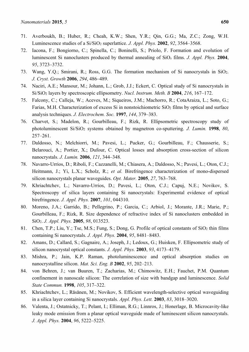
Nanomaterials 2015, 5 650
71. Averboukh, B.; Huber, R.; Cheah, K.W.; Shen, Y.R.; Qin, G.G.; Ma, Z.C.; Zong, W.H.
Luminescence studies of a Si/SiO2 superlattice. J. Appl. Phys. 2002, 92, 3564–3568.
72. Iacona, F.; Bongiorno, C.; Spinella, C.; Boninelli, S.; Priolo, F. Formation and evolution of
luminescent Si nanoclusters produced by thermal annealing of SiOx films. J. Appl. Phys. 2004,
95, 3723–3732.
73. Wang, Y.Q.; Smirani, R.; Ross, G.G. The formation mechanism of Si nanocrystals in SiO2.
J. Cryst. Growth 2006, 294, 486–489.
74. Naciri, A.E.; Mansour, M.; Johann, L.; Grob, J.J.; Eckert, C. Optical study of Si nanocrystals in
Si/SiO2 layers by spectroscopic ellipsometry. Nucl. Instrum. Meth. B 2004, 216, 167–172.
75. Falcony, C.; Calleja, W.; Aceves, M.; Siqueiros, J.M.; Machorro, R.; CotaAraiza, L.; Soto, G.;
Farias, M.H. Characterization of excess Si in nonstoichiometric SiO2 films by optical and surface
analysis techniques. J. Electrochem. Soc. 1997, 144, 379–383.
76. Charvet, S.; Madelon, R.; Gourbilleau, F.; Rizk, R. Ellipsometric spectroscopy study of
photoluminescent Si/SiO2 systems obtained by magnetron co-sputtering. J. Lumin. 1998, 80,
257–261.
77. Daldosso, N.; Melchiorri, M.; Pavesi, L.; Pucker, G.; Gourbilleau, F.; Chausserie, S.;
Belarouci, A.; Portier, X.; Dufour, C. Optical losses and absorption cross-section of silicon
nanocrystals. J. Lumin. 2006, 121, 344–348.
78. Navarro-Urrios, D.; Riboli, F.; Cazzanelli, M.; Chiasera, A.; Daldosso, N.; Pavesi, L.; Oton, C.J.;
Heitmann, J.; Yi, L.X.; Scholz, R.; et al. Birefringence characterization of mono-dispersed
silicon nanocrystals planar waveguides. Opt. Mater. 2005, 27, 763–768.
79. Khriachtchev, L.; Navarro-Urrios, D.; Pavesi, L.; Oton, C.J.; Capuj, N.E.; Novikov, S.
Spectroscopy of silica layers containing Si nanocrystals: Experimental evidence of optical
birefringence. J. Appl. Phys. 2007, 101, 044310.
80. Moreno, J.A.; Garrido, B.; Pellegrino, P.; Garcia, C.; Arbiol, J.; Morante, J.R.; Marie, P.;
Gourbilleau, F.; Rizk, R. Size dependence of refractive index of Si nanoclusters embedded in
SiO2. J. Appl. Phys. 2005, 98, 013523.
81. Chen, T.P.; Liu, Y.; Tse, M.S.; Fung, S.; Dong, G. Profile of optical constants of SiO2 thin films
containing Si nanocrystals. J. Appl. Phys. 2004, 95, 8481–8483.
82. Amans, D.; Callard, S.; Gagnaire, A.; Joseph, J.; Ledoux, G.; Huisken, F. Ellipsometric study of
silicon nanocrystal optical constants. J. Appl. Phys. 2003, 93, 4173–4179.
83. Mishra, P.; Jain, K.P. Raman, photoluminescence and optical absorption studies on
nanocrystalline silicon. Mat. Sci. Eng. B 2002, 95, 202–213.
84. von Behren, J.; van Buuren, T.; Zacharias, M.; Chimowitz, E.H.; Fauchet, P.M. Quantum
confinement in nanoscale silicon: The correlation of size with bandgap and luminescence. Solid
State Commun. 1998, 105, 317–322.
85. Khriachtchev, L.; Räsänen, M.; Novikov, S. Efficient wavelength-selective optical waveguiding
in a silica layer containing Si nanocrystals. Appl. Phys. Lett. 2003, 83, 3018–3020.
86. Valenta, J.; Ostatnicky, T.; Pelant, I.; Elliman, R.G.; Linnros, J.; Honerlage, B. Microcavity-like
leaky mode emission from a planar optical waveguide made of luminescent silicon nanocrystals.
J. Appl. Phys. 2004, 96, 5222–5225.
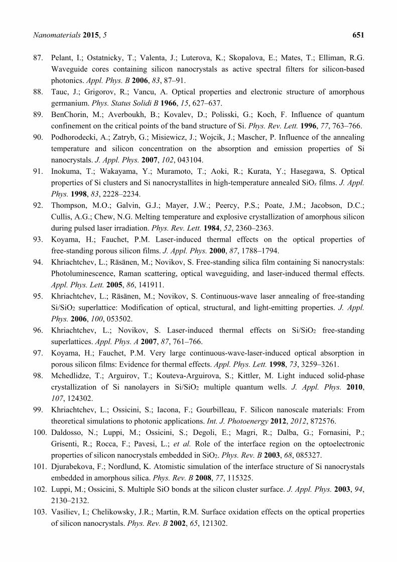
Nanomaterials 2015, 5 651
87. Pelant, I.; Ostatnicky, T.; Valenta, J.; Luterova, K.; Skopalova, E.; Mates, T.; Elliman, R.G.
Waveguide cores containing silicon nanocrystals as active spectral filters for silicon-based
photonics. Appl. Phys. B 2006, 83, 87–91.
88. Tauc, J.; Grigorov, R.; Vancu, A. Optical properties and electronic structure of amorphous
germanium. Phys. Status Solidi B 1966, 15, 627–637.
89. BenChorin, M.; Averboukh, B.; Kovalev, D.; Polisski, G.; Koch, F. Influence of quantum
confinement on the critical points of the band structure of Si. Phys. Rev. Lett. 1996, 77, 763–766.
90. Podhorodecki, A.; Zatryb, G.; Misiewicz, J.; Wojcik, J.; Mascher, P. Influence of the annealing
temperature and silicon concentration on the absorption and emission properties of Si
nanocrystals. J. Appl. Phys. 2007, 102, 043104.
91. Inokuma, T.; Wakayama, Y.; Muramoto, T.; Aoki, R.; Kurata, Y.; Hasegawa, S. Optical
properties of Si clusters and Si nanocrystallites in high-temperature annealed SiOx films. J. Appl.
Phys. 1998, 83, 2228–2234.
92. Thompson, M.O.; Galvin, G.J.; Mayer, J.W.; Peercy, P.S.; Poate, J.M.; Jacobson, D.C.;
Cullis, A.G.; Chew, N.G. Melting temperature and explosive crystallization of amorphous silicon
during pulsed laser irradiation. Phys. Rev. Lett. 1984, 52, 2360–2363.
93. Koyama, H.; Fauchet, P.M. Laser-induced thermal effects on the optical properties of
free-standing porous silicon films. J. Appl. Phys. 2000, 87, 1788–1794.
94. Khriachtchev, L.; Räsänen, M.; Novikov, S. Free-standing silica film containing Si nanocrystals:
Photoluminescence, Raman scattering, optical waveguiding, and laser-induced thermal effects.
Appl. Phys. Lett. 2005, 86, 141911.
95. Khriachtchev, L.; Räsänen, M.; Novikov, S. Continuous-wave laser annealing of free-standing
Si/SiO2 superlattice: Modification of optical, structural, and light-emitting properties. J. Appl.
Phys. 2006, 100, 053502.
96. Khriachtchev, L.; Novikov, S. Laser-induced thermal effects on Si/SiO2 free-standing
superlattices. Appl. Phys. A 2007, 87, 761–766.
97. Koyama, H.; Fauchet, P.M. Very large continuous-wave-laser-induced optical absorption in
porous silicon films: Evidence for thermal effects. Appl. Phys. Lett. 1998, 73, 3259–3261.
98. Mchedlidze, T.; Arguirov, T.; Kouteva-Arguirova, S.; Kittler, M. Light induced solid-phase
crystallization of Si nanolayers in Si/SiO2 multiple quantum wells. J. Appl. Phys. 2010,
107, 124302.
99. Khriachtchev, L.; Ossicini, S.; Iacona, F.; Gourbilleau, F. Silicon nanoscale materials: From
theoretical simulations to photonic applications. Int. J. Photoenergy 2012, 2012, 872576.
100. Daldosso, N.; Luppi, M.; Ossicini, S.; Degoli, E.; Magri, R.; Dalba, G.; Fornasini, P.;
Grisenti, R.; Rocca, F.; Pavesi, L.; et al. Role of the interface region on the optoelectronic
properties of silicon nanocrystals embedded in SiO2. Phys. Rev. B 2003, 68, 085327.
101. Djurabekova, F.; Nordlund, K. Atomistic simulation of the interface structure of Si nanocrystals
embedded in amorphous silica. Phys. Rev. B 2008, 77, 115325.
102. Luppi, M.; Ossicini, S. Multiple SiO bonds at the silicon cluster surface. J. Appl. Phys. 2003, 94,
2130–2132.
103. Vasiliev, I.; Chelikowsky, J.R.; Martin, R.M. Surface oxidation effects on the optical properties
of silicon nanocrystals. Phys. Rev. B 2002, 65, 121302.
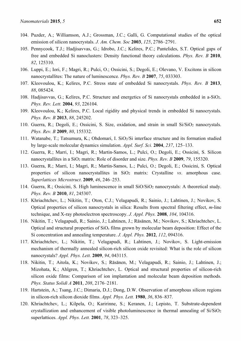
Nanomaterials 2015, 5 652
104. Puzder, A.; Williamson, A.J.; Grossman, J.C.; Galli, G. Computational studies of the optical
emission of silicon nanocrystals. J. Am. Chem. Soc 2003, 125, 2786–2791.
105. Pennycook, T.J.; Hadjisavvas, G.; Idrobo, J.C.; Kelires, P.C.; Pantelides, S.T. Optical gaps of
free and embedded Si nanoclusters: Density functional theory calculations. Phys. Rev. B 2010,
82, 125310.
106. Luppi, E.; Iori, F.; Magri, R.; Pulci, O.; Ossicini, S.; Degoli, E.; Olevano, V. Excitons in silicon
nanocrystallites: The nature of luminescence. Phys. Rev. B 2007, 75, 033303.
107. Kleovoulou, K.; Kelires, P.C. Stress state of embedded Si nanocrystals. Phys. Rev. B 2013,
88, 085424.
108. Hadjisavvas, G.; Kelires, P.C. Structure and energetics of Si nanocrystals embedded in a-SiO2.
Phys. Rev. Lett. 2004, 93, 226104.
109. Kleovoulou, K.; Kelires, P.C. Local rigidity and physical trends in embedded Si nanocrystals.
Phys. Rev. B 2013, 88, 245202.
110. Guerra, R.; Degoli, E.; Ossicini, S. Size, oxidation, and strain in small Si/SiO2 nanocrystals.
Phys. Rev. B 2009, 80, 155332.
111. Watanabe, T.; Tatsumura, K.; Ohdomari, I. SiO2/Si interface structure and its formation studied
by large-scale molecular dynamics simulation. Appl. Surf. Sci. 2004, 237, 125–133.
112. Guerra, R.; Marri, I.; Magri, R.; Martin-Samos, L.; Pulci, O.; Degoli, E.; Ossicini, S. Silicon
nanocrystallites in a SiO2 matrix: Role of disorder and size. Phys. Rev. B 2009, 79, 155320.
113. Guerra, R.; Marri, I.; Magri, R.; Martin-Samos, L.; Pulci, O.; Degoli, E.; Ossicini, S. Optical
properties of silicon nanocrystallites in SiO2 matrix: Crystalline vs. amorphous case.
Superlattices Microstruct. 2009, 46, 246–253.
114. Guerra, R.; Ossicini, S. High luminescence in small SiO/SiO2 nanocrystals: A theoretical study.
Phys. Rev. B 2010, 81, 245307.
115. Khriachtchev, L.; Nikitin, T.; Oton, C.J.; Velagapudi, R.; Sainio, J.; Lahtinen, J.; Novikov, S.
Optical properties of silicon nanocrystals in silica: Results from spectral filtering effect, m-line
technique, and X-ray photoelectron spectroscopy. J. Appl. Phys. 2008, 104, 104316.
116. Nikitin, T.; Velagapudi, R.; Sainio, J.; Lahtinen, J.; Räsänen, M.; Novikov, S.; Khriachtchev, L.
Optical and structural properties of SiOx films grown by molecular beam deposition: Effect of the
Si concentration and annealing temperature. J. Appl. Phys. 2012, 112, 094316.
117. Khriachtchev, L.; Nikitin, T.; Velagapudi, R.; Lahtinen, J.; Novikov, S. Light-emission
mechanism of thermally annealed silicon-rich silicon oxide revisited: What is the role of silicon
nanocrystals? Appl. Phys. Lett. 2009, 94, 043115.
118. Nikitin, T.; Aitola, K.; Novikov, S.; Räsänen, M.; Velagapudi, R.; Sainio, J.; Lahtinen, J.;
Mizohata, K.; Ahlgren, T.; Khriachtchev, L. Optical and structural properties of silicon-rich
silicon oxide films: Comparison of ion implantation and molecular beam deposition methods.
Phys. Status Solidi A 2011, 208, 2176–2181.
119. Hartstein, A.; Tsang, J.C.; Dimaria, D.J.; Dong, D.W. Observation of amorphous silicon regions
in silicon-rich silicon dioxide films. Appl. Phys. Lett. 1980, 36, 836–837.
120. Khriachtchev, L.; Kilpela, O.; Karirinne, S.; Keranen, J.; Lepisto, T. Substrate-dependent
crystallization and enhancement of visible photoluminescence in thermal annealing of Si/SiO2
superlattices. Appl. Phys. Lett. 2001, 78, 323–325.
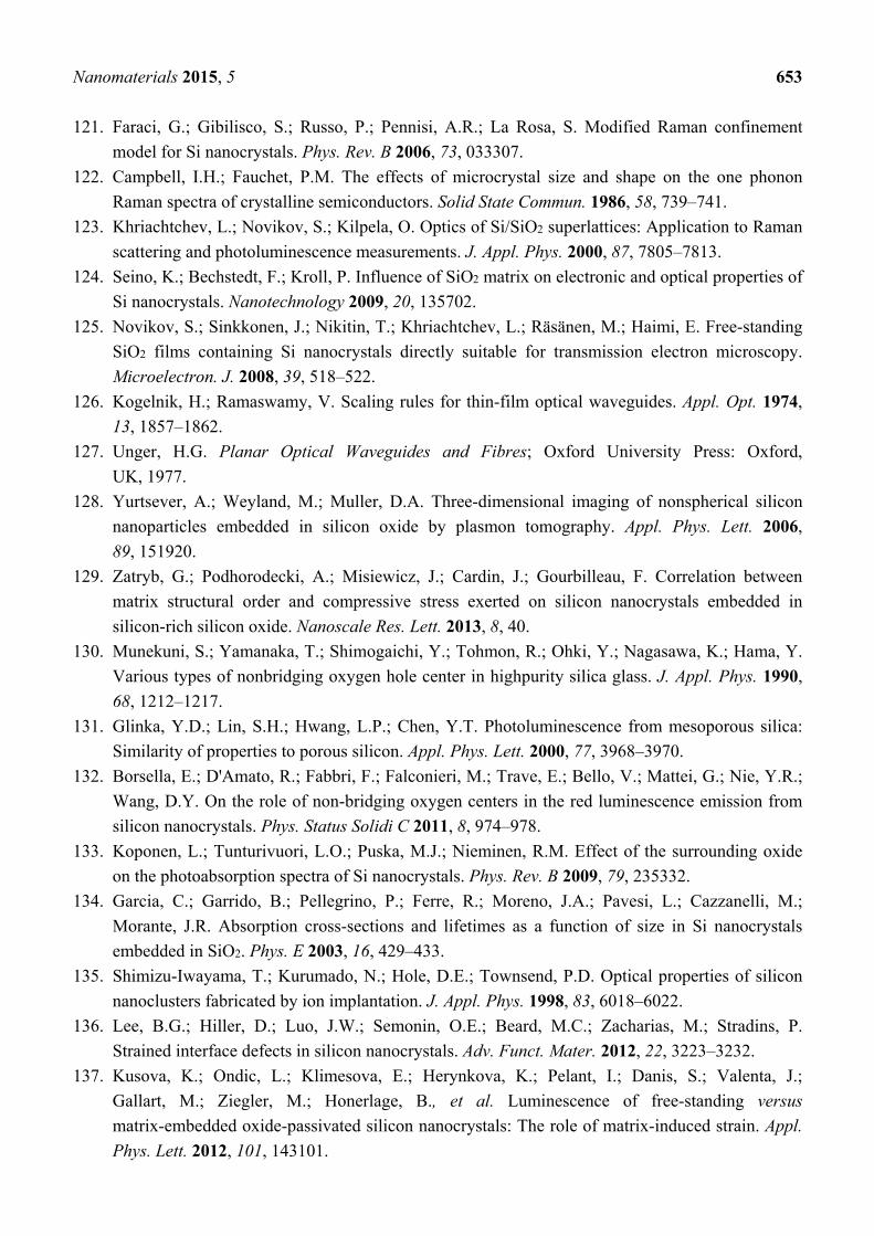
Nanomaterials 2015, 5 653
121. Faraci, G.; Gibilisco, S.; Russo, P.; Pennisi, A.R.; La Rosa, S. Modified Raman confinement
model for Si nanocrystals. Phys. Rev. B 2006, 73, 033307.
122. Campbell, I.H.; Fauchet, P.M. The effects of microcrystal size and shape on the one phonon
Raman spectra of crystalline semiconductors. Solid State Commun. 1986, 58, 739–741.
123. Khriachtchev, L.; Novikov, S.; Kilpela, O. Optics of Si/SiO2 superlattices: Application to Raman
scattering and photoluminescence measurements. J. Appl. Phys. 2000, 87, 7805–7813.
124. Seino, K.; Bechstedt, F.; Kroll, P. Influence of SiO2 matrix on electronic and optical properties of
Si nanocrystals. Nanotechnology 2009, 20, 135702.
125. Novikov, S.; Sinkkonen, J.; Nikitin, T.; Khriachtchev, L.; Räsänen, M.; Haimi, E. Free-standing
SiO2 films containing Si nanocrystals directly suitable for transmission electron microscopy.
Microelectron. J. 2008, 39, 518–522.
126. Kogelnik, H.; Ramaswamy, V. Scaling rules for thin-film optical waveguides. Appl. Opt. 1974,
13, 1857–1862.
127. Unger, H.G. Planar Optical Waveguides and Fibres; Oxford University Press: Oxford,
UK, 1977.
128. Yurtsever, A.; Weyland, M.; Muller, D.A. Three-dimensional imaging of nonspherical silicon
nanoparticles embedded in silicon oxide by plasmon tomography. Appl. Phys. Lett. 2006,
89, 151920.
129. Zatryb, G.; Podhorodecki, A.; Misiewicz, J.; Cardin, J.; Gourbilleau, F. Correlation between
matrix structural order and compressive stress exerted on silicon nanocrystals embedded in
silicon-rich silicon oxide. Nanoscale Res. Lett. 2013, 8, 40.
130. Munekuni, S.; Yamanaka, T.; Shimogaichi, Y.; Tohmon, R.; Ohki, Y.; Nagasawa, K.; Hama, Y.
Various types of nonbridging oxygen hole center in highpurity silica glass. J. Appl. Phys. 1990,
68, 1212–1217.
131. Glinka, Y.D.; Lin, S.H.; Hwang, L.P.; Chen, Y.T. Photoluminescence from mesoporous silica:
Similarity of properties to porous silicon. Appl. Phys. Lett. 2000, 77, 3968–3970.
132. Borsella, E.; D'Amato, R.; Fabbri, F.; Falconieri, M.; Trave, E.; Bello, V.; Mattei, G.; Nie, Y.R.;
Wang, D.Y. On the role of non-bridging oxygen centers in the red luminescence emission from
silicon nanocrystals. Phys. Status Solidi C 2011, 8, 974–978.
133. Koponen, L.; Tunturivuori, L.O.; Puska, M.J.; Nieminen, R.M. Effect of the surrounding oxide
on the photoabsorption spectra of Si nanocrystals. Phys. Rev. B 2009, 79, 235332.
134. Garcia, C.; Garrido, B.; Pellegrino, P.; Ferre, R.; Moreno, J.A.; Pavesi, L.; Cazzanelli, M.;
Morante, J.R. Absorption cross-sections and lifetimes as a function of size in Si nanocrystals
embedded in SiO2. Phys. E 2003, 16, 429–433.
135. Shimizu-Iwayama, T.; Kurumado, N.; Hole, D.E.; Townsend, P.D. Optical properties of silicon
nanoclusters fabricated by ion implantation. J. Appl. Phys. 1998, 83, 6018–6022.
136. Lee, B.G.; Hiller, D.; Luo, J.W.; Semonin, O.E.; Beard, M.C.; Zacharias, M.; Stradins, P.
Strained interface defects in silicon nanocrystals. Adv. Funct. Mater. 2012, 22, 3223–3232.
137. Kusova, K.; Ondic, L.; Klimesova, E.; Herynkova, K.; Pelant, I.; Danis, S.; Valenta, J.;
Gallart, M.; Ziegler, M.; Honerlage, B., et al. Luminescence of free-standing versus
matrix-embedded oxide-passivated silicon nanocrystals: The role of matrix-induced strain. Appl.
Phys. Lett. 2012, 101, 143101.
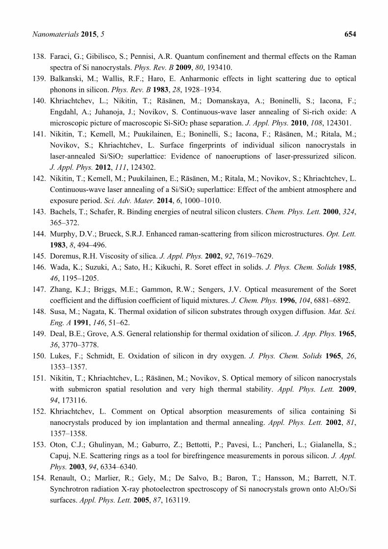
Nanomaterials 2015, 5 654
138. Faraci, G.; Gibilisco, S.; Pennisi, A.R. Quantum confinement and thermal effects on the Raman
spectra of Si nanocrystals. Phys. Rev. B 2009, 80, 193410.
139. Balkanski, M.; Wallis, R.F.; Haro, E. Anharmonic effects in light scattering due to optical
phonons in silicon. Phys. Rev. B 1983, 28, 1928–1934.
140. Khriachtchev, L.; Nikitin, T.; Räsänen, M.; Domanskaya, A.; Boninelli, S.; Iacona, F.;
Engdahl, A.; Juhanoja, J.; Novikov, S. Continuous-wave laser annealing of Si-rich oxide: A
microscopic picture of macroscopic Si-SiO2 phase separation. J. Appl. Phys. 2010, 108, 124301.
141. Nikitin, T.; Kemell, M.; Puukilainen, E.; Boninelli, S.; Iacona, F.; Räsänen, M.; Ritala, M.;
Novikov, S.; Khriachtchev, L. Surface fingerprints of individual silicon nanocrystals in
laser-annealed Si/SiO2 superlattice: Evidence of nanoeruptions of laser-pressurized silicon.
J. Appl. Phys. 2012, 111, 124302.
142. Nikitin, T.; Kemell, M.; Puukilainen, E.; Räsänen, M.; Ritala, M.; Novikov, S.; Khriachtchev, L.
Continuous-wave laser annealing of a Si/SiO2 superlattice: Effect of the ambient atmosphere and
exposure period. Sci. Adv. Mater. 2014, 6, 1000–1010.
143. Bachels, T.; Schafer, R. Binding energies of neutral silicon clusters. Chem. Phys. Lett. 2000, 324,
365–372.
144. Murphy, D.V.; Brueck, S.R.J. Enhanced raman-scattering from silicon microstructures. Opt. Lett.
1983, 8, 494–496.
145. Doremus, R.H. Viscosity of silica. J. Appl. Phys. 2002, 92, 7619–7629.
146. Wada, K.; Suzuki, A.; Sato, H.; Kikuchi, R. Soret effect in solids. J. Phys. Chem. Solids 1985,
46, 1195–1205.
147. Zhang, K.J.; Briggs, M.E.; Gammon, R.W.; Sengers, J.V. Optical measurement of the Soret
coefficient and the diffusion coefficient of liquid mixtures. J. Chem. Phys. 1996, 104, 6881–6892.
148. Susa, M.; Nagata, K. Thermal oxidation of silicon substrates through oxygen diffusion. Mat. Sci.
Eng. A 1991, 146, 51–62.
149. Deal, B.E.; Grove, A.S. General relationship for thermal oxidation of silicon. J. App. Phys. 1965,
36, 3770–3778.
150. Lukes, F.; Schmidt, E. Oxidation of silicon in dry oxygen. J. Phys. Chem. Solids 1965, 26,
1353–1357.
151. Nikitin, T.; Khriachtchev, L.; Räsänen, M.; Novikov, S. Optical memory of silicon nanocrystals
with submicron spatial resolution and very high thermal stability. Appl. Phys. Lett. 2009,
94, 173116.
152. Khriachtchev, L. Comment on Optical absorption measurements of silica containing Si
nanocrystals produced by ion implantation and thermal annealing. Appl. Phys. Lett. 2002, 81,
1357–1358.
153. Oton, C.J.; Ghulinyan, M.; Gaburro, Z.; Bettotti, P.; Pavesi, L.; Pancheri, L.; Gialanella, S.;
Capuj, N.E. Scattering rings as a tool for birefringence measurements in porous silicon. J. Appl.
Phys. 2003, 94, 6334–6340.
154. Renault, O.; Marlier, R.; Gely, M.; De Salvo, B.; Baron, T.; Hansson, M.; Barrett, N.T.
Synchrotron radiation X-ray photoelectron spectroscopy of Si nanocrystals grown onto Al2O3/Si
surfaces. Appl. Phys. Lett. 2005, 87, 163119.
Nanomaterials 2015, 5 655
155. Kim, S.; Kim, M.C.; Choi, S.H.; Kim, K.J.; Hwang, H.N.; Hwang, C.C. Size dependence of Si 2p
core-level shift at Si nanocrystal/SiO2 interfaces. Appl. Phys. Lett. 2007, 91, 103113.
156. Barbagiovanni, E.G.; Goncharova, L.V.; Simpson, P.J. Electronic structure study of ion-implanted
Si quantum dots in a SiO2 matrix: Analysis of quantum confinement theories. Phys. Rev. B 2011,
83, 035112.
157. Bruggeman, D.A.G. Berechnung verschiedener physikalischer Konstanten von heterogenen
Substanzen. I. Dielektrizitätskonstanten und Leitfähigkeiten der Mischkörper aus isotropen
Substanzen. Ann. Phys. 1935, 416, 636–664.
158. Knief, S.; von Niessen, W. Disorder, defects, and optical absorption in a-Si and a-Si:H. Phys.
Rev. B 1999, 59, 12940–12946.
© 2015 by the authors; licensee MDPI, Basel, Switzerland. This article is an open access article
distributed under the terms and conditions of the Creative Commons Attribution license
(http://creativecommons.org/licenses/by/4.0/).