optical fault masking attacks - university of cambridgesps32/fdtc2010-masking.pdfoptical fault...
TRANSCRIPT
Optical Fault Masking Attacks
Sergei Skorobogatov Computer Laboratory
University of Cambridge Cambridge, United Kingdom
e-mail: [email protected]
Abstract—This paper introduces some new types of optical fault attacks called fault masking attacks. These attacks are aimed at disrupting of the normal memory operation through preventing changes of the memory contents. The technique was demonstrated on an EEPROM and Flash memory inside PIC microcontrollers. Then it was improved with a backside approach and tested on a PIC and MSP430 microcontrollers. These attacks can be used for the partial reverse engineering of semiconductor chips by spotting the areas of activity in reprogrammable non-volatile memory. This can assist in data analysis and other types of fault injection attacks later, thereby saving the time otherwise required for exhaustive search. Practical limits for optical fault masking attacks in terms of sample preparation, operating conditions and chip technology are discussed, together with possible countermeasures.
Keywords: optical fault attacks; semi-invasive methods; hardware security; write protection; tamper resistance
I. INTRODUCTION Sensitive information, which includes encryption keys
and passwords, is stored in non-volatile memory like EEPROM and Flash. Intermediate results during encryption, signature verification and password checking are stored in SRAM memory. Inducing faults during memory write operation could result in the leakage of sensitive information. Memory modification attacks were proposed as a serious threat to semiconductor devices in the late nineties [1], for example, by leaking a signing key [2]. Since then, several practical ways of implementing such attacks were announced, most notably semi-invasive attacks [3]. These do not require expensive and time-consuming preparation techniques as the passivation layer of the chip remains intact. Also, they do not cause any mechanical damage to the silicon of the device, so they are reversible in most cases. So far they were demonstrated in the form of UV attacks [4] and fault injection attacks [5]. However, many fault attacks were applied in the form of injecting external signals during the operation of a device. For example, glitch attacks were aimed at forcing the CPU into a wrong execution path [6]. Other kinds of fault attacks were aimed at changing the contents of memory [7] or flipping bits in registers [5]. Fault injection attacks in the form of blocking the EEPROM write operation were used in the late nineties for breaking security in smartcards [4]. However, this field has hardly been explored for modern smartcards which lack an external programming voltage supply. In this paper, I present the results of an investigation on what an attacker could possibly do by influencing the internal memory
write and erase operations inside a semiconductor chip using simple optical fault injection attacks. Such influence could result in the blocking of write and erase operations in EEPROM and Flash memory. These kinds of fault injection attacks are called the fault masking attacks.
In a publication on optically enhanced power analysis attacks [8], it was shown that a laser with a certain power can influence the operation of embedded SRAM causing certain memory cells to keep their state independently whether a new value was written into it. The research presented in this paper demonstrates that a similar effect can be achieved for embedded non-volatile memory like EEPROM and Flash used in various microcontrollers. Not only the old near 1 μm chips were fallible to the attack, but also a modern 0.35 μm microcontroller. This is not the first time such effect on non-volatile memory was observed. Discovery of optical fault injection attacks back in 2001 [5] was sparked by the disruption of EEPROM operation in a tested smartcard [3]. However, no further research was made in this direction till now. If optical fault masking attacks become easily reproducible, this could pose a big problem to the hardware community as it will allow the blocking re-write operation to certain parts of the embedded memory. Without countermeasures in place such attacks could potentially break the security of a chip.
This paper is organised as follows. Section 2 gives brief introduction into on-chip memories and optical fault injection attacks. Section 3 introduces the experimental setup, while Section 4 shows the results. Section 5 discusses limits and possible ways of improvement. Some possible countermeasures are presented in the concluding section.
II. BACKGROUND In order to implement optical attacks on CMOS
transistors, the chip surface needs to be accessible. Early optical attacks were demonstrated with light from a photo flash [5]. To influence each memory cell independently, a more focusable source of ionizing radiation is preferable, such as a laser beam [9].
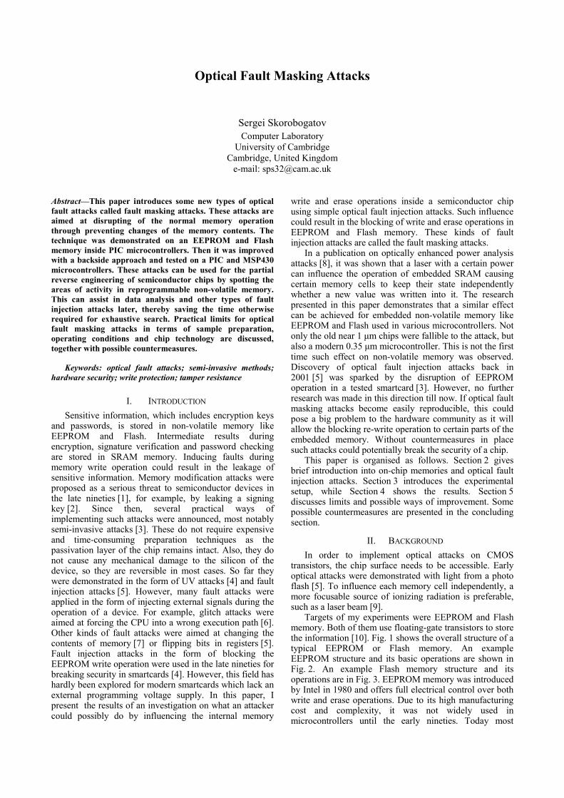
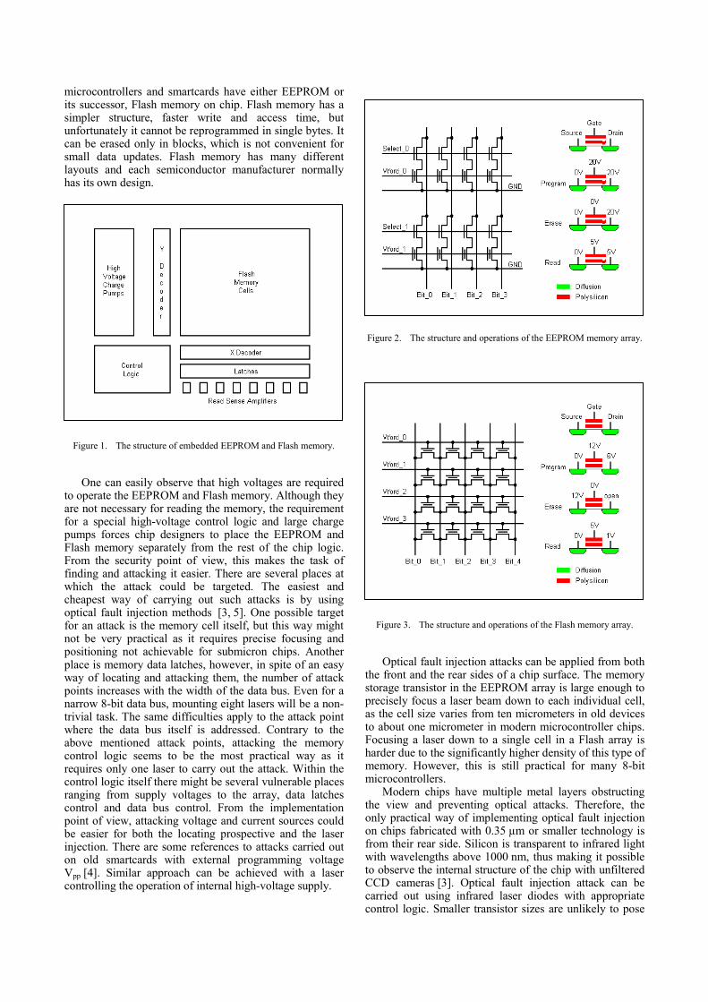
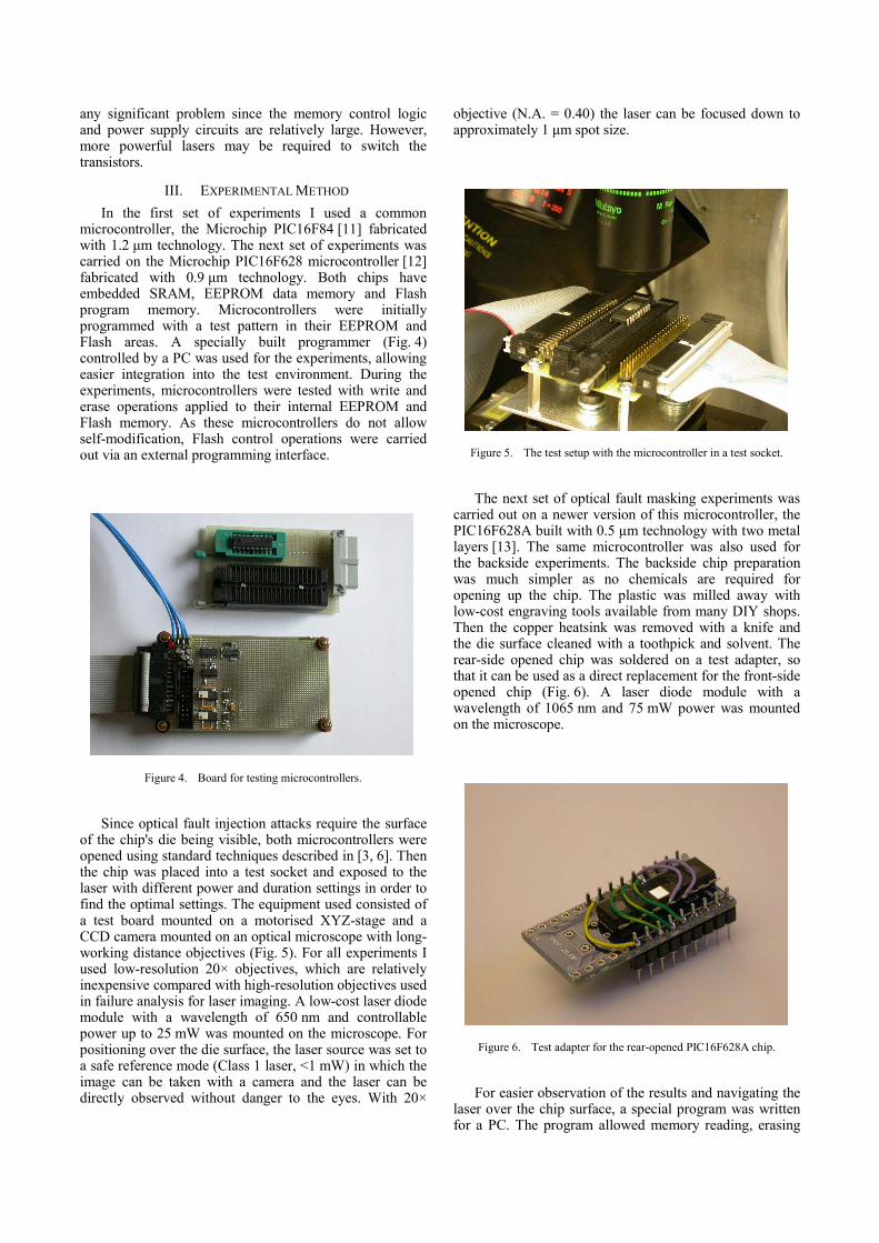
Targets of my experiments were EEPROM and Flash memory. Both of them use floating-gate transistors to store the information [10]. Fig. 1 shows the overall structure of a typical EEPROM or Flash memory. An example EEPROM structure and its basic operations are shown in Fig. 2. An example Flash memory structure and its operations are in Fig. 3. EEPROM memory was introduced by Intel in 1980 and offers full electrical control over both write and erase operations. Due to its high manufacturing cost and complexity, it was not widely used in microcontrollers until the early nineties. Today most
microcontrollers and smartcards have either EEPROM or its successor, Flash memory on chip. Flash memory has a simpler structure, faster write and access time, but unfortunately it cannot be reprogrammed in single bytes. It can be erased only in blocks, which is not convenient for small data updates. Flash memory has many different layouts and each semiconductor manufacturer normally has its own design.
Figure 1. The structure of embedded EEPROM and Flash memory.
One can easily observe that high voltages are required
to operate the EEPROM and Flash memory. Although they are not necessary for reading the memory, the requirement for a special high-voltage control logic and large charge pumps forces chip designers to place the EEPROM and Flash memory separately from the rest of the chip logic. From the security point of view, this makes the task of finding and attacking it easier. There are several places at which the attack could be targeted. The easiest and cheapest way of carrying out such attacks is by using optical fault injection methods [3, 5]. One possible target for an attack is the memory cell itself, but this way might not be very practical as it requires precise focusing and positioning not achievable for submicron chips. Another place is memory data latches, however, in spite of an easy way of locating and attacking them, the number of attack points increases with the width of the data bus. Even for a narrow 8-bit data bus, mounting eight lasers will be a non-trivial task. The same difficulties apply to the attack point where the data bus itself is addressed. Contrary to the above mentioned attack points, attacking the memory control logic seems to be the most practical way as it requires only one laser to carry out the attack. Within the control logic itself there might be several vulnerable places ranging from supply voltages to the array, data latches control and data bus control. From the implementation point of view, attacking voltage and current sources could be easier for both the locating prospective and the laser injection. There are some references to attacks carried out on old smartcards with external programming voltage Vpp [4]. Similar approach can be achieved with a laser controlling the operation of internal high-voltage supply.
Figure 2. The structure and operations of the EEPROM memory array.
Figure 3. The structure and operations of the Flash memory array.
Optical fault injection attacks can be applied from both
the front and the rear sides of a chip surface. The memory storage transistor in the EEPROM array is large enough to precisely focus a laser beam down to each individual cell, as the cell size varies from ten micrometers in old devices to about one micrometer in modern microcontroller chips. Focusing a laser down to a single cell in a Flash array is harder due to the significantly higher density of this type of memory. However, this is still practical for many 8-bit microcontrollers.
Modern chips have multiple metal layers obstructing the view and preventing optical attacks. Therefore, the only practical way of implementing optical fault injection on chips fabricated with 0.35 µm or smaller technology is from their rear side. Silicon is transparent to infrared light with wavelengths above 1000 nm, thus making it possible to observe the internal structure of the chip with unfiltered CCD cameras [3]. Optical fault injection attack can be carried out using infrared laser diodes with appropriate control logic. Smaller transistor sizes are unlikely to pose
any significant problem since the memory control logic and power supply circuits are relatively large. However, more powerful lasers may be required to switch the transistors.
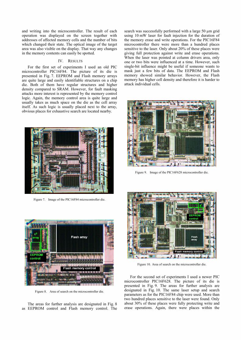
III. EXPERIMENTAL METHOD In the first set of experiments I used a common
microcontroller, the Microchip PIC16F84 [11] fabricated with 1.2 μm technology. The next set of experiments was carried on the Microchip PIC16F628 microcontroller [12] fabricated with 0.9 μm technology. Both chips have embedded SRAM, EEPROM data memory and Flash program memory. Microcontrollers were initially programmed with a test pattern in their EEPROM and Flash areas. A specially built programmer (Fig. 4) controlled by a PC was used for the experiments, allowing easier integration into the test environment. During the experiments, microcontrollers were tested with write and erase operations applied to their internal EEPROM and Flash memory. As these microcontrollers do not allow self-modification, Flash control operations were carried out via an external programming interface.
Figure 4. Board for testing microcontrollers.
Since optical fault injection attacks require the surface
of the chip's die being visible, both microcontrollers were opened using standard techniques described in [3, 6]. Then the chip was placed into a test socket and exposed to the laser with different power and duration settings in order to find the optimal settings. The equipment used consisted of a test board mounted on a motorised XYZ-stage and a CCD camera mounted on an optical microscope with long-working distance objectives (Fig. 5). For all experiments I used low-resolution 20× objectives, which are relatively inexpensive compared with high-resolution objectives used in failure analysis for laser imaging. A low-cost laser diode module with a wavelength of 650 nm and controllable power up to 25 mW was mounted on the microscope. For positioning over the die surface, the laser source was set to a safe reference mode (Class 1 laser, <1 mW) in which the image can be taken with a camera and the laser can be directly observed without danger to the eyes. With 20×
objective (N.A. = 0.40) the laser can be focused down to approximately 1 μm spot size.
Figure 5. The test setup with the microcontroller in a test socket.
The next set of optical fault masking experiments was
carried out on a newer version of this microcontroller, the PIC16F628A built with 0.5 µm technology with two metal layers [13]. The same microcontroller was also used for the backside experiments. The backside chip preparation was much simpler as no chemicals are required for opening up the chip. The plastic was milled away with low-cost engraving tools available from many DIY shops. Then the copper heatsink was removed with a knife and the die surface cleaned with a toothpick and solvent. The rear-side opened chip was soldered on a test adapter, so that it can be used as a direct replacement for the front-side opened chip (Fig. 6). A laser diode module with a wavelength of 1065 nm and 75 mW power was mounted on the microscope.
Figure 6. Test adapter for the rear-opened PIC16F628A chip.
For easier observation of the results and navigating the
laser over the chip surface, a special program was written for a PC. The program allowed memory reading, erasing
and writing into the microcontroller. The result of each operation was displayed on the screen together with addresses of affected memory cells and the number of bits which changed their state. The optical image of the target area was also visible on the display. That way any changes in the memory contents can easily be spotted.
IV. RESULTS For the first set of experiments I used an old PIC
microcontroller PIC16F84. The picture of its die is presented in Fig. 7. EEPROM and Flash memory arrays are quite large and easily identifiable structures on a chip die. Both of them have regular structures and higher density compared to SRAM. However, for fault masking attacks more interest is represented by the memory control logic. Again, the memory control area is quite large and usually takes as much space on the die as the cell array itself. As such logic is usually placed next to the array, obvious places for exhaustive search are located nearby.
Figure 7. Image of the PIC16F84 microcontroller die.
Figure 8. Area of search on the microcontroller die.
The areas for further analysis are designated in Fig. 8
as EEPROM control and Flash memory control. The
search was successfully performed with a large 50 µm grid using 10 mW laser for fault injection for the duration of the memory erase and write operations. For the PIC16F84 microcontroller there were more than a hundred places sensitive to the laser. Only about 20% of these places were giving full protection against write and erase operations. When the laser was pointed at column drivers area, only one or two bits were influenced at a time. However, such single-bit influence might be useful if someone wants to mask just a few bits of data. The EEPROM and Flash memory showed similar behavior. However, the Flash memory has higher cell density and therefore it is harder to attack individual cells.
Figure 9. Image of the PIC16F628 microcontroller die.
Figure 10. Area of search on the microcontroller die.
For the second set of experiments I used a newer PIC
microcontroller PIC16F628. The picture of its die is presented in Fig. 9. The areas for further analysis are designated in Fig. 10. The same laser setup and search parameters as for the PIC16F84 chip were used. More than two hundred places sensitive to the laser were found. Only about 30% of these places were fully protecting write and erase operations. Again, there were places within the
columns control logic that allowed bitwise control over the data.
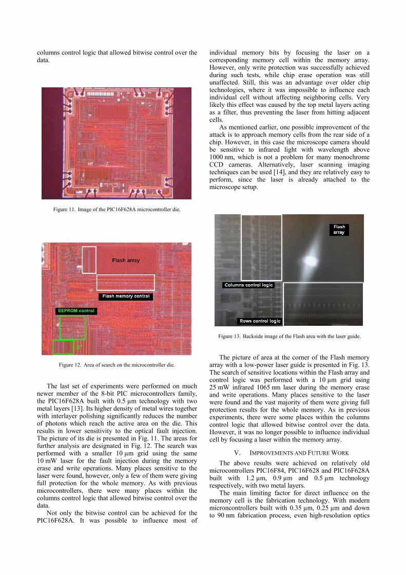
Figure 11. Image of the PIC16F628A microcontroller die.
Figure 12. Area of search on the microcontroller die.
The last set of experiments were performed on much
newer member of the 8-bit PIC microcontrollers family, the PIC16F628A built with 0.5 µm technology with two metal layers [13]. Its higher density of metal wires together with interlayer polishing significantly reduces the number of photons which reach the active area on the die. This results in lower sensitivity to the optical fault injection. The picture of its die is presented in Fig. 11. The areas for further analysis are designated in Fig. 12. The search was performed with a smaller 10 µm grid using the same 10 mW laser for the fault injection during the memory erase and write operations. Many places sensitive to the laser were found, however, only a few of them were giving full protection for the whole memory. As with previous microcontrollers, there were many places within the columns control logic that allowed bitwise control over the data.
Not only the bitwise control can be achieved for the PIC16F628A. It was possible to influence most of
individual memory bits by focusing the laser on a corresponding memory cell within the memory array. However, only write protection was successfully achieved during such tests, while chip erase operation was still unaffected. Still, this was an advantage over older chip technologies, where it was impossible to influence each individual cell without affecting neighboring cells. Very likely this effect was caused by the top metal layers acting as a filter, thus preventing the laser from hitting adjacent cells.
As mentioned earlier, one possible improvement of the attack is to approach memory cells from the rear side of a chip. However, in this case the microscope camera should be sensitive to infrared light with wavelength above 1000 nm, which is not a problem for many monochrome CCD cameras. Alternatively, laser scanning imaging techniques can be used [14], and they are relatively easy to perform, since the laser is already attached to the microscope setup.
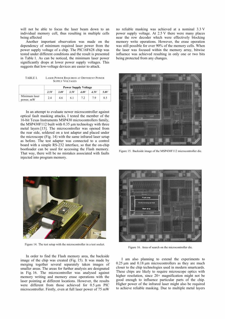
Figure 13. Backside image of the Flash area with the laser guide.
The picture of area at the corner of the Flash memory
array with a low-power laser guide is presented in Fig. 13. The search of sensitive locations within the Flash array and control logic was performed with a 10 µm grid using 25 mW infrared 1065 nm laser during the memory erase and write operations. Many places sensitive to the laser were found and the vast majority of them were giving full protection results for the whole memory. As in previous experiments, there were some places within the columns control logic that allowed bitwise control over the data. However, it was no longer possible to influence individual cell by focusing a laser within the memory array.
V. IMPROVEMENTS AND FUTURE WORK The above results were achieved on relatively old
microcontrollers PIC16F84, PIC16F628 and PIC16F628A built with 1.2 µm, 0.9 µm and 0.5 µm technology respectively, with two metal layers.
The main limiting factor for direct influence on the memory cell is the fabrication technology. With modern microncontrollers built with 0.35 µm, 0.25 µm and down to 90 nm fabrication process, even high-resolution optics
will not be able to focus the laser beam down to an individual memory cell, thus resulting in multiple cells being affected
Another important observation was made on the dependency of minimum required laser power from the power supply voltage of a chip. The PIC16F628 chip was tested under different conditions and the result is presented in Table 1. As can be noticed, the minimum laser power significantly drops at lower power supply voltages. This suggests that low-voltage devices are easier to attack.
TABLE I. LASER POWER REQUIRED AT DIFFERENT POWER SUPPLY VOLTAGES
Power Supply Voltage
2.5V 3.0V 3.5V 4.0V 4.5V 5.0V Minimum laser power, mW
2.4 4.6 6.1 7.2 7.9 8.5
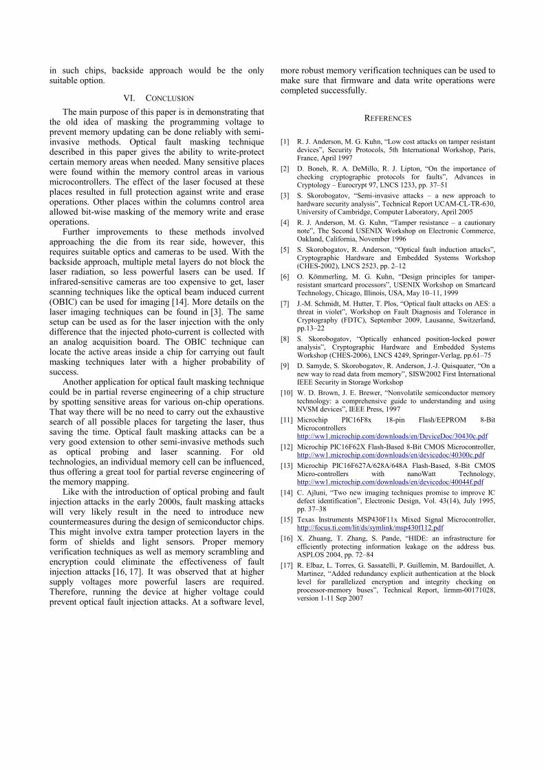
In an attempt to evaluate newer microcontroller against
optical fault masking attacks, I tested the member of the 16-bit Texas Instruments MSP430 microcontrollers family, the MSP430F112 built with 0.35 µm technology with three metal layers [15]. The microcontroller was opened from the rear side, soldered on a test adapter and placed under the microscope (Fig. 14) with the same infrared laser setup as before. The test adapter was connected to a control board with a simple RS-232 interface, so that the on-chip bootloader can be used for accessing the Flash memory. That way, there will be no mistakes associated with faults injected into program memory.
Figure 14. The test setup with the microcontroller in a test socket.
In order to find the Flash memory area, the backside
image of the chip was created (Fig. 15). It was made by merging together several separately taken images of smaller areas. The areas for further analysis are designated in Fig. 16. The microcontroller was analysed against memory writing and memory erase operations with the laser pointing at different locations. However, the results were different from those achieved for 0.5 µm PIC microcontroller. Firstly, even at full laser power of 75 mW
no reliable masking was achieved at a nominal 3.3 V power supply voltage. At 2.5 V there were many places near the row decoder which were effectively blocking memory write operations. However, the erase operation was still possible for over 90% of the memory cells. When the laser was focused within the memory array, bitwise influence was achieved resulting in only one or two bits being protected from any changes.
Figure 15. Backside image of the MSP430F112 microcontroller die.
Figure 16. Area of search on the microcontroller die.
I am also planning to extend the experiments to
0.25 μm and 0.18 μm microcontrollers as they are much closer to the chip technologies used in modern smartcards. These chips are likely to require microscope optics with higher resolution, since 20× magnification might not be good enough to influence particular parts of the chip. Higher power of the infrared laser might also be required to achieve reliable masking. Due to multiple metal layers
in such chips, backside approach would be the only suitable option.
VI. CONCLUSION The main purpose of this paper is in demonstrating that
the old idea of masking the programming voltage to prevent memory updating can be done reliably with semi-invasive methods. Optical fault masking technique described in this paper gives the ability to write-protect certain memory areas when needed. Many sensitive places were found within the memory control areas in various microcontrollers. The effect of the laser focused at these places resulted in full protection against write and erase operations. Other places within the columns control area allowed bit-wise masking of the memory write and erase operations.
Further improvements to these methods involved approaching the die from its rear side, however, this requires suitable optics and cameras to be used. With the backside approach, multiple metal layers do not block the laser radiation, so less powerful lasers can be used. If infrared-sensitive cameras are too expensive to get, laser scanning techniques like the optical beam induced current (OBIC) can be used for imaging [14]. More details on the laser imaging techniques can be found in [3]. The same setup can be used as for the laser injection with the only difference that the injected photo-current is collected with an analog acquisition board. The OBIC technique can locate the active areas inside a chip for carrying out fault masking techniques later with a higher probability of success.
Another application for optical fault masking technique could be in partial reverse engineering of a chip structure by spotting sensitive areas for various on-chip operations. That way there will be no need to carry out the exhaustive search of all possible places for targeting the laser, thus saving the time. Optical fault masking attacks can be a very good extension to other semi-invasive methods such as optical probing and laser scanning. For old technologies, an individual memory cell can be influenced, thus offering a great tool for partial reverse engineering of the memory mapping.
Like with the introduction of optical probing and fault injection attacks in the early 2000s, fault masking attacks will very likely result in the need to introduce new countermeasures during the design of semiconductor chips. This might involve extra tamper protection layers in the form of shields and light sensors. Proper memory verification techniques as well as memory scrambling and encryption could eliminate the effectiveness of fault injection attacks [16, 17]. It was observed that at higher supply voltages more powerful lasers are required. Therefore, running the device at higher voltage could prevent optical fault injection attacks. At a software level,
more robust memory verification techniques can be used to make sure that firmware and data write operations were completed successfully.
REFERENCES
[1] R. J. Anderson, M. G. Kuhn, “Low cost attacks on tamper resistant devices”, Security Protocols, 5th International Workshop, Paris, France, April 1997
[2] D. Boneh, R. A. DeMillo, R. J. Lipton, “On the importance of checking cryptographic protocols for faults”, Advances in Cryptology – Eurocrypt 97, LNCS 1233, pp. 37–51
[3] S. Skorobogatov, “Semi-invasive attacks – a new approach to hardware security analysis”, Technical Report UCAM-CL-TR-630, University of Cambridge, Computer Laboratory, April 2005
[4] R. J. Anderson, M. G. Kuhn, “Tamper resistance – a cautionary note”, The Second USENIX Workshop on Electronic Commerce, Oakland, California, November 1996
[5] S. Skorobogatov, R. Anderson, “Optical fault induction attacks”, Cryptographic Hardware and Embedded Systems Workshop (CHES-2002), LNCS 2523, pp. 2–12
[6] O. Kömmerling, M. G. Kuhn, “Design principles for tamper-resistant smartcard processors”, USENIX Workshop on Smartcard Technology, Chicago, Illinois, USA, May 10–11, 1999
[7] J.-M. Schmidt, M. Hutter, T. Plos, “Optical fault attacks on AES: a threat in violet”, Workshop on Fault Diagnosis and Tolerance in Cryptography (FDTC), September 2009, Lausanne, Switzerland, pp.13–22
[8] S. Skorobogatov, “Optically enhanced position-locked power analysis”, Cryptographic Hardware and Embedded Systems Workshop (CHES-2006), LNCS 4249, Springer-Verlag, pp.61–75
[9] D. Samyde, S. Skorobogatov, R. Anderson, J.-J. Quisquater, “On a new way to read data from memory”, SISW2002 First International IEEE Security in Storage Workshop
[10] W. D. Brown, J. E. Brewer, “Nonvolatile semiconductor memory technology: a comprehensive guide to understanding and using NVSM devices”, IEEE Press, 1997
[11] Microchip PIC16F8x 18-pin Flash/EEPROM 8-Bit Microcontrollers http://ww1.microchip.com/downloads/en/DeviceDoc/30430c.pdf
[12] Microchip PIC16F62X Flash-Based 8-Bit CMOS Microcontroller, http://ww1.microchip.com/downloads/en/devicedoc/40300c.pdf
[13] Microchip PIC16F627A/628A/648A Flash-Based, 8-Bit CMOS Micro-controllers with nanoWatt Technology, http://ww1.microchip.com/downloads/en/devicedoc/40044f.pdf
[14] C. Ajluni, “Two new imaging techniques promise to improve IC defect identification”, Electronic Design, Vol. 43(14), July 1995, pp. 37–38
[15] Texas Instruments MSP430F11x Mixed Signal Microcontroller, http://focus.ti.com/lit/ds/symlink/msp430f112.pdf
[16] X. Zhuang, T. Zhang, S. Pande, “HIDE: an infrastructure for efficiently protecting information leakage on the address bus. ASPLOS 2004, pp. 72–84
[17] R. Elbaz, L. Torres, G. Sassatelli, P. Guillemin, M. Bardouillet, A. Martinez, “Added redundancy explicit authentication at the block level for parallelized encryption and integrity checking on processor-memory buses”, Technical Report, lirmm-00171028, version 1-11 Sep 2007