optical interconnection technology in switches, routers, and optical cross connects
TRANSCRIPT

20 Optical Networks Magazine July/August 2003
Opticalinterconnectiontechnology inswitches,routers, andoptical crossconnects
Magnus JonssonSchool of Information Science,Computer and Electrical EngineeringHalmstad UniversityHalmstad, Sweden
1 Introduction
Novel optical technologies offer possibilities fornew solutions for the increasing bandwidthdemands of data communication and telecom-
munication equipment. This paper uses a primarilyarchitectural approach to explore the possibilities ofusing optical interconnections in such equipment. Someselected groups of concepts are selected here in order togive a reasonably broad view in the scope of a singlepaper.
The interconnection architectures are evaluatedaccording to three system types with different switchingtime requirements. These types are: (i) optical cross con-nects (OXCs), (ii) switches and routers with some kind ofburst switching and (iii) switches and routers that redirecttraffic on the packet or cell level.
OXCs have relatively slow timing requirements, i.e. inthe order of milliseconds or even tens of milliseconds. Onthe other hand, it is valuable if the signals remain optical allthe way through the switch, including possible queuingsystems, i.e. there is optical transparency. In this way it iseasier to scale up the bit rate or change protocols.
With burst switching, packets with the same destin-ation, like the same exterior gateway, can be groupedtogether to reduce switching time requirements. This hasfor instance been discussed for use in all-optical packetswitching [1,2]. The switching time requirements are inthe order of sub-microseconds.
For pure switching at the packet level, the switchingtime requirements are in the order of nanoseconds. Withlonger switching times, the overhead between the packetswill be too large. All-optical packet switching has beenproposed but much work remains to reach purely opticalrouters [1]. However, some experiments have been doneand several architectures that are more or less purelyoptical have been proposed [3-7].
The interconnection networks reviewed are intendedfor use in, or as substitution of, the switch core in data ortelecommunication equipment. Other components neededin addition to the switch core vary between differentequipment. As an example, a simple switch might beimplemented without much more components, while an IProuter needs components to manage the routing table. Theacceptable cost of an interconnection network can also varydepending on whether it is to be used in a core router,where many users share the cost, or in equipment near theend-user.
Another driving application domain for opticalsystem-level interconnections, in addition to data and
ABSTRACTThe performance of data- and telecommunication equip-ment must keep abreast of the increasing network speed.At the same time, it is necessary to deal with the internalinterconnection complexity, which typically grows by N2
or NlogN, where N is the number of ports. This requiresnew interconnection technologies to be used internally inthe equipment. Optical interconnection technology is apromising alternative and much work has already beendone. This paper reviews a number of optical and opto-electronic interconnection architectures, especially froma data and telecommunication equipment point of view.Three kinds of systems for adopting optical interconnec-tion technology are discussed: (i) optical cross connects(OXCs), (ii) switches and routers with some kind of burstswitching and (iii) switches and routers that redirect traf-fic on the packet or cell level. The interconnection tech-nologies and architectures are discussed according totheir suitability for adoption in the three system types.
5138454 6/23/03 10:44 AM Page 20
Copyright 2003 Society of Photo-Optical Instrumentation Engineers and Kluwer Academic Publishers.This paper was published in Optical Network Magazine and is made available as an electronic reprint withpermission of SPIE and KAP. One print or electronic copy may be made for personal use only. Systematicor multiple reproduction, distribution to multiple locations via electronic or other means, duplication of anymaterial in this paper for a fee or for commercial purposes, or modification of the content of the paper are prohibited.

Optical Networks Magazine July/August 2003 21
telecommunication equipment, is parallel and distrib-uted computing systems [8-11]. Important work in thefield of optical interconnections in computing andcommunications started in the mid 1980s. Of theearly publications, a good paper on system aspects waspublished by Goodman et al. in 1984 [12], while pub-lications by Miller et al. can represent work on specificcomponents. Other examples of early work in the fieldare [13-16].
The rest of the paper is organized as follows. Switchfabrics are generally reviewed in Section 2, and Section 3describes optical link technologies. Section 4 presentsfiber-optic interconnection networks. Integrated opticalinterconnection systems and optical and optoelectronicswitch-fabrics are described in Sections 5 and 6, respect-ively. Sections 7 and 8 give a discussion and a summary,respectively.
2 Switch FabricsAn example of a switch or router is shown in
Figure 1, where the switch fabric transfers traffic frominput ports to output ports on the basis of decisionsmade by some control logic. One of the simplest ways toimplement or simulate an electrical switch fabric is tohave a shared medium to which I/O interfaces, controlprocessors or the like are attached and over which thetraffic is time multiplexed (see Figure 2). A common wayof implementing a shared-medium network is to use thebus topology, where only one node is allowed to send ata time, but a shared-medium network can also be a ringfor example. The great advantage of a shared-mediumnetwork is the easy implementation of broadcast, whichis useful in many situations. The disadvantage is that thebandwidth does not scale with the number of nodes(ports on a switch).
The crossbar is the most flexible switch fabricand can be compared with a fully connected topology,i.e. all possible pairs of input and output ports areconnected by point-to-point connections. The draw-back, however, is the increase by N 2 in cost/complexityof the switch, where N is the number of ports. Systemswith a single electrical true crossbar are thereforelimited to small or medium-sized systems. A 140 �140 � 3.2 Gbit/s single-chip switch is commerciallyavailable [17].
In multistage shuffle-exchange networks, the costfunction is reduced to N log2 N, but here log2 N stagesmust be traversed to reach the desired output port. Anexample of this kind of a network is the Omega network(Figure 3), which provides exactly one path from anyinput to any output. The different switch functions of the2 � 2 switch that is used as the building block are shownin Figure 4, where the two right most configurations areused for broadcast. Switches larger than 2 � 2 can also beused. Each stage of the switches in an Omega network ispreceded by a perfect-shuffle interconnection pattern. Incontrast to a crossbar network, which is a nonblockingnetwork, an Omega network is a blocking network. Thismeans that there may not always exist a path through thenetwork as a result of already existing paths that block theway. Rearrangeable networks are another category ofmultistage networks where it is always possible to find apath through the network. However, if all paths are notrouted at the same time, it may be necessary to reroutealready existing paths.
3 Optical Link TechnologiesThis section discusses two main categories of optical
links, fiber-ribbon links and bit-parallel WDM links. Sin-gle-channel single-fiber solutions are not treated.
Figure 1: An example of switch architecture.
Figure 2: Bus-based switch architecture.
Figure 3: Eight-channel Omega network. One path through thenetwork is highlighted.
Figure 4: Possible states of a 2 � 2 switch.
5138454 6/23/03 10:44 AM Page 21

22 Optical Networks Magazine July/August 2003
3.1 Fiber-ribbon linksA system component that reached the market some
years ago is the fiber-ribbon link. As an example of anearly commercial link, the Motorola OPTOBUS hasten parallel fibers, each carrying data at a bit rate of400 Mbit/s, which gives an aggregated bandwidth of4 Gbit/s [18]. Bi-directional links are also possible, wheresome fibers in the fiber-ribbon cables are dedicated foreach direction [19]. Further references to reports on fiber-ribbon links are found in [20].
In scaling up the bandwidth of a fiber-ribbon linkwhere a dedicated fiber carries the clock signal, the mainproblem is channel-to-channel skew. The skew is mainlythe result of differences in propagation delay betweendifferent fibers and variations of lasing delay time amongdifferent laser diodes [21]. The 400 Mbit/s OPTOBUShas a specified maximum skew of 200 ps, excluding thefiber-ribbon cable for which 6 ps/m is assumed for stand-ard ribbons [18]. Even though the distances are rathershort in the systems discussed in this paper, the scalingto higher speeds calls for a discussion of techniques toreduce the effect of the skew.
One technique is to actually reduce the skew, eitherby using low skew ribbons or employing skew compen-sation. Fiber ribbons with a skew below 1 ps/m havebeen developed [22], which essentially increases thepossible bandwidth distance product. All the fibers inthe same ribbon are sequentially cut to reduce thevariation in refractive index among the fibers. In thefiber-ribbon link described in [23], a dedicated fibercarries a clock signal used to clock data on 31 fibers.The transmitter circuitry for each channel has a pro-grammable clock skew adjustment to adjust the clock in80-ps increments.
Another technique is to extract the clock signal fromthe bit flow on each fiber instead of using a separate fiberto carry the clock signal. The disadvantage is increasedhardware complexity when a clock recovery circuit anda buffer circuit for each channel in the receiver are added.A hybrid solution is to skip the separate clock channeland encode clock information on the data channels whilestill sending in bit-parallel mode, as reported in [24]. Inthis case, a deskew unit relying on FIFO registers (FirstIn First Out) ensures that parallel data words that are out-put from the receiver are identical to those which weresent. A possible � 15-ns deskew was reported. A similarsystem is reported in [25].
The techniques mentioned above introduce eitherincreased hardware complexity or a more sophisticatedfiber-ribbon manufacturing process. If the manufactur-ing process allows for adding more fibers in each rib-bon, this may be a cheaper alternative. For example,a fiber-ribbon link with 32 fibers, each with a bit rateof 500 Mbit/s, was described in [23], and researchersat NEC have developed a module in which 8 � 2 lasersare coupled to two fiber-ribbons [26]. Links with
48 channels [27] and 72 channels (36 in each direction)[28] have recently appeared on the market. Instead offiber ribbons, fiber imaging guides (FIGs) with thou-sands of pixels can be used [29]. In the system describedin [30], both a 14000-pixel FIG and a 3500-pixel FIGwere coupled to an 8 � 8 VCSEL (Vertical CavitySurface Emitting Laser) array in different set-ups. Overshort communication distances, the fiber ribbon caneven be replaced by some optical elements to obtainfree-space communication. A 256-channel bidirectionalintra-PCB (Printed Circuit Board) free-space intercon-nection system is described in [31].
3.2 Bit-Parallel WDM LinksA bit-parallel WDM link is another way to
synchronously transmit on several channels in parallel. Inthis way we get bit-parallel byte-serial transmission [32].However, compensation for bit skew caused by groupdelay dispersion, where different wavelength channelstravel at different speeds in the fiber, may be needed inthese systems [33].
A dedicated wavelength in a bit-parallel WDMlink can be used for clock information. Wavelengths, orfibers in a fiber-ribbon cable, can also be dedicated toother purposes such as frame synchronization and flowcontrol. Significantly higher bandwidth distance prod-ucts can be achieved when using bit-parallel WDM overdispersion-shifted fiber instead of fiber-ribbons [34]. If,however, there is only communication over shorterdistances, like a few meters, the bandwidth distanceproduct is not necessarily a limiting factor. Transmissionexperiments with an array of eight pie-shaped VCSELsarranged in a circular area with a diameter of 60 �m, tomatch the core of a multimode fiber, have been reported[35]. Other work on the integration of componentsfor short distance WDM links has been reported,e.g. a 4 � 2.5 Gbit/s transceiver with integrated splitter,combiner, filters etc. [36].
4 Fiber-Optic Interconnection NetworksFiber-optic network architectures, especially passive
ones, are discussed below. First, different basic passivefiber-optic network architectures are described. WDMstar, WDM ring, and AWG networks are then respec-tively discussed. Fiber-ribbon ring networks are pre-sented last.
4.1 Passive Fiber-Optic NetworksIn an all-optical network, the data stream remains
in the optical form all the way from the transmitter tothe receiver. Three basic architectures for all-opticalmulti-access networks are the ring, the bus and thestar (see Figure 5). These will be discussed below.Most work on passive optical networks has focused onLANs or similar structures but they can also be used as
5138454 6/23/03 10:44 AM Page 22

Optical Networks Magazine July/August 2003 23
Figure 5: Passive optical network architectures: (a) ring, (b) (dual)bus, and (c) star.
substitutes for switch fabrics in data and telecommuni-cation equipment. It should be noted that if one ofthese networks is used in an OXC or the like as a switchfabric, the signal is normally converted to electrical andback to optical form at the entrance and the exit of theswitch fabric.
An all-optical multiple-access ring network differsfrom a traditional ring network in the sense that all othernodes can be reached in a single hop without any inter-mediate optoelectronic conversion. Only a fraction ofthe optical power contained in the bypassing fiber istapped to the receiver, which gives all nodes theopportunity to read the message. In other words, multi-cast or broadcast is possible. Outgoing messages areinserted into the ring. A node removes its own messagesfrom the ring after one round.
In an optical bus, the light travels only in one direc-tion, making two buses necessary (upper and lower),one for each direction (higher or lower node index ofdestination nodes). This kind of bus architectureis called dual bus. The disadvantage of the dual bus isthat two transceivers are needed in each node. Thisis avoided in the folded bus, where the two buses areconnected with a wrap-around connection at one end ofthe buses (see Figure 6). In the folded bus, transmittersand receivers are connected to the upper and lower bus,respectively.
In a star network, the incoming light waves from allnodes are combined and uniformly distributed back tothe nodes. In other words, the optical power contained inthe middle of the star is equally divided between all nodes.
All of the three basic network architectures offerdifferent advantages. The ring has the least amount offibers, a bus network’s medium access protocol can utilizethe linear ordering of the nodes, and the star has the bestpower budget in practice. Star networks are the mostpopular, however, judging from the number of publishedreports.
While passive optical networks that offer only oneshared channel are not promising alternatives, they formthe basis for more powerful networks using WDM.These networks can be promising solutions as switchfabrics in some kinds of data and telecommunicationequipment.
4.2 WDM starBy using WDM, multiple wavelength channels can
carry data simultaneously in the network. Figure 7 showsan example of a WDM star network configuration. Eachnode transmits on a wavelength unique to the node, whilethe receiver can listen to an arbitrary wavelength [37].One can say that this kind of network architecture imple-ments a distributed crossbar. The flexibility is hence high,and multicast and single-destination traffic can co-exist.WDM star networks have been proposed especially forinternal use in packet switches [38-41].
Tunable components with tuning latencies in theorder of a nanosecond have been reported, but they oftenhave a limited tuning range [42]. At the expense of longertuning latencies, however, components with a broadertuning range can be used [43]. Such components can beused to achieve a cheaper network in systems where muchof the communication patterns remain constant for alonger period.
Complete removal of the ability to tune in a WDMstar network gives a multi-hop network [44]. Each nodein a multi-hop network transmits and receives on one ora few dedicated wavelengths. If a node does not have thecapability of sending on one of the receiver wavelengthsof the destination node, the traffic must pass one orseveral intermediate nodes. The wavelengths can, forexample, be chosen to get a perfect-shuffle network [45].A network in which several topologies, like a ring and
Figure 6: Folded fiber-optic bus. Figure 7: WDM star network.
5138454 6/23/03 10:44 AM Page 23

24 Optical Networks Magazine July/August 2003
Figure 8: WDM star multi-hop network.
Figure 9: Multi-hop topology.
Figure 10: AWG network.
Figure 11: Ring network as switch-fabric.
a hypercube, are embedded can also be chosen. An exam-ple of a multi-hop network is shown in Figure 8. Thisconfiguration of wavelength assignments corresponds tothe topology shown in Figure 9.
4.3 WDM ringA WDM ring network utilizes ADMs (Add Drop
Multiplexers) in all nodes to insert to, listen to andremove wavelength channels from the ring. In theWDMA ring network described in [46], each node isassigned a node-unique wavelength on which to trans-mit. The other nodes can then tune in an arbitrarychannel on which to listen. This configuration is log-ically the same as that of the WDM star network withfixed transmitters and tunable receivers. The distributedcrossbar again gives good performance for generalcommunication patterns.
4.4 AWG networksAWG (Arrayed Waveguide Grating) networks are
related to WDM star networks, but here the passiveoptical star is exchanged with an AWG [47]. The AWGroutes wavelengths such that spatial reuse of wavelengthsis possible, as seen in Figure 10. Only N wavelengths (�A,�B, �C, and �D,) are needed to get a fully connected N �N network with N 2 optical channels (�A1, �A2, . . .�D4). The AWGs have been proposed for use both as
a stand-alone network component [48] and as a compo-nent in routers [4].
4.5 Fiber-ribbon pipeline ring networkBit-parallel transfer can be utilized when fiber-ribbon
links are used to connect the nodes in a point-to-pointlinked ring network. In such a network, one of the fibers ineach ribbon is dedicated to carrying the clock signal thusmaking clock-recovery circuits unnecessary in the receivers.Other fibers can be utilized for frame synchronization andother control purposes. Figure 11 shows how a ring net-work is used as a switch fabric.
As seen in Figure 12, aggregated throughputs higherthan 1 can be obtained in ring networks with support forspatial bandwidth reuse, sometimes called pipeline rings.This feature can be effectively used when most of thecommunication is to the nearest downstream neighbor.Two fiber-ribbon pipeline ring networks have recently beenreported [49]. The first has support for circuit switching
Figure 12: Example of spatial bandwidth reuse. Node M sends toNode 1 at the same time that Node 1 sends to Node 2 and Node 2sends a multicast packet to Nodes 3, 4, and 5.
5138454 6/23/03 10:44 AM Page 24

Optical Networks Magazine July/August 2003 25
Figure 13: Control channel based network built up with fiber-ribbon point-to-point links.
Figure 14: A foil of fibers connects four nodes and distributesclock signals to them.
on 8 � 1 fibers (data and clock) and packet switching onan additional fiber. The second network is more flexibleand has support for packet switching on 8 � 1 fibers anduses a tenth fiber for control packets (see Figure 13). Thecontrol packets carry MAC information for the collision-less MAC protocol with support for slot reserving. Slotreserving can be used to get RTVCs (Real-Time VirtualChannels) for which guaranteed bandwidth and a worst-case latency are specified (compare with circuit switching).The fiber-ribbon ring network can offer rather highthroughputs due to the aggregated bandwidth of a fiber-ribbon cable, especially when there is a great deal of nearestdownstream neighbor communication. However, thespatial reuse will probably be limited if used in dataor telecommunication equipment owing to more evenlydistributed destinations as compared to the parallel com-puting systems for which the network was first proposed.
Another fiber-ribbon ring network is the PONInetwork (formerly USC POLO), which is proposed foruse in clusters of workstations and similar systems[50,51]. Integrated circuits have been developed for thenetwork, and tests have been done [52,53].
5 Integrated Optical InterconnectionSystems
This section describes three types of more orless purely integrated optical interconnection systems.This type of interconnection system can be used to inter-connect electronic switch chips or I/O interfaces. Inte-grated fiber and waveguide solutions, planar free spaceoptics, and free space optical backplanes are discussed.
5.1 Integrated fiber and waveguidesolutions
Fibers or other kinds of waveguides (hereafter com-monly denoted as channels) can be integrated to form amore or less compact system of channels. Fibers can belaminated to form a foil of channels for use as intra-PCBor back-plane interconnection systems [54-56]. Fiber-ribbon connectors are applied to fiber end-points of thefoil. An example is shown in Figure 14, where four nodesare connected in a ring topology. The medium is simply
changed into an even more compact variant of the fiber-ribbon ring network. In addition, there is a clock that dis-tributes clock signals to the four nodes via equal lengthfibers to keep the clock signals in phase. In other words,a fiber-optic clock distribution network and a data net-work are integrated into one system. If one foil is placedon each PCB in a rack, they can be passively connected toeach other via fiber-ribbon cables or a backplane foil.Using polymer waveguides instead of fibers offers advan-tages such as the possibility of integrating splitters andcombiners into the foil and the potential for more costeffective mass production [54].
Another way is to follow the proposed use of an arrayof passive optical stars to connect processor boards in amultiprocessor system via fiber-ribbon links, for whichexperiments with 6 � 700 Mbit/s fiber-ribbon links weredone (see Figure 15) [57]. Of course, the processorsboards can be exchanged with transceiver cards and/orswitch cards. As indicated above, such a configuration canbe integrated by the use of polymer waveguides. Thepower budget can, however, be a limiting factor to thenumber of nodes and/or the distance. Advantages aresimple hardware owing to bit-parallel transmission, likeother fiber-ribbon solutions, and the broadcast nature, butthe star array can become a bottleneck as in all bus-likesystems. In a similar system, the star array is exchangedwith a chip with optoelectronics that has one incomingribbon from each node and one output ribbon [58]. Theoutput ribbon is coupled to an array of 1 � N couplers so
Figure 15: An array of passive optical stars connects a number ofnodes via fiber-ribbon cables.
5138454 6/23/03 10:44 AM Page 25

26 Optical Networks Magazine July/August 2003
Figure 17: Optical backplane configurations: (a) with planar freespace optics, (b) with smart pixel arrays, and (c) with a mirror.
that each node has a ribbon connected to its receiver. Thechip couples the incoming traffic together in a way thatsimulates a bus. At contention, the chip can temporarilystore packets.
Other similar systems include the integration offibers into a PCB for the purpose of clock distribu-tion [59]. Distribution to up to 128 nodes was demon-strated. The fibers are laminated on one side of thePCB, while integrated circuits are placed on the reverseside. The end section of each fiber is bent 90 degrees tolead the light through a so called via hole to the reverseside of the PCB.
5.2 Planar free space opticsPlacing electronic chips, including optoelectronic de-
vices, and optical elements on a substrate where light beamscan travel gives a planar free space system (Figure 16)[60-61]. Electronic chips are placed in a 2-dimensionalplane, while light beams travel in a 3-dimensional space. Inthis way, optical systems can be integrated monolithically,which gives compact, stable and potentially inexpensive sys-tems [61]. A flexible network can be obtained by using spa-tial light modulators to dynamically direct the optical beams.Using only fixed interconnection patterns and electronicswitching can give shorter switch times, however. A planarfree space optical crossbar switch has been reported [62].
5.3 Free space optical backplanesSeveral different optical backplanes have been pro-
posed, three of which are discussed below. As shown in Fig-ure 17a, using planar free space optics is one means oftransporting optical signals between PCBs. Holographicgratings can be used to insert/extract the optical signalsto/from the waveguide, which may be a glass substrate [63].Several beams or bus lines can be used so each arrow in thefigure represents several parallel beams [64].
In the system shown in Figure 17b, 2-dimensionalarrays of optical beams (typically 10 000) link neighboringPCBs together in a point-to-point fashion [65]. Smart pixelarrays then act as intelligent routers that can, e.g., bypassdata or perform data extraction operations where some datapass to the local PCB and some data are retransmitted tothe next PCB [66]. Each smart pixel array can typicallycontain 1 000 smart pixels arranged in a 2-dimensionalarray, where each pixel has a receiver, a transmitter, and asimple processing unit. One way to configure the system is
to connect the smart pixel arrays in a ring, where the ringcan be reconfigured to embed other topologies [67].
The configuration shown in Figure 17c is similar tothe optical backplane based on planar free space intercon-nects, but the waveguide is replaced here by a mirror [68].An optical beam leaving a transmitter is simply bouncedonce on the mirror before it arrives at the receiver.A regeneration of the optical signal might be needed onthe way from the source to the final destination.
Of the three types of optical backplanes discussed,the one with smart pixel arrays seems to be the mostpowerful. On the other hand, a simple passive opticalbackplane may have other advantages. Other opticalbackplanes proposed include a bus where optical signalscan pass through transparent photo detectors or bemodulated by spatial light modulators [69].
6 Optical and OptoelectronicSwitch-Fabrics
This section introduces optical and optoelectronicswitch-fabrics. The combination of optical interconnec-tions and electronic crossbars is treated first and a dis-cussion is then presented of WDM/SDM switches.
6.1 Optical interconnections and electroniccrossbars
The switch itself can be modified to increase per-formance or packing density. A single-chip switch corewhere fiber-ribbons are coupled directly to optoelec-tronic devices on the chip is possible [70]. Attaching 32incoming and 32 outgoing fiber-ribbons with 800Mbit/s per fiber translates to an aggregated bandwidth of204 Gbit/s through the switch when there are eight datafibers per link.
Figure 16: Example of a planar free space system. The beam direc-tion is steered by the optical element on its way between two chips.
5138454 6/23/03 10:44 AM Page 26

Optical Networks Magazine July/August 2003 27
A 16 � 16 crossbar switch chip with integrated opto-electronic I/O was implemented for switching packetstransferred using bit-parallel WDM [71]. Each node hastwo single-mode fibers coupled to the switch, one for inputand one for output. Another switch system supporting anarbitrary topology uses 8 � 8 crossbars, where a 12-channelfiber-ribbon link is connected to each port [72]. The aggre-gated throughput of a single switch is 64 Gbit/s. Multistagenetworks with free-space interconnections between elec-tronic crossbars have also been reported [10,73,74]. Chipsor multi-chip-modules with surface-attached optical I/Oare stacked to obtain a 3-dimensional multistage system.
6.2 WDM/SDM switchesThe architecture with optical interconnections and
electronic crossbars is flexible and powerful. In addition tosimply in the I/O interface or as optical interconnectionsbetween electronic crossbars, optics and optoelectronicscan also be used internally in a switch fabric, however.A broad spectrum of solutions has been proposed, andsome examples are given below.
SDM (Space Division Multiplexing) switches [13,75-77] and WDM switches (with, e.g. wavelength convertersand wavelength selective components) [78–79] can beused both as stand-alone switches and as buildingcomponents in larger switch fabrics [80]. As an example, aBanyan multistage network built of 2 � 2 LiNbO3 switchelements has been described [81-82], while a crossbarequivalent system is described in [83]. Another multistagenetwork uses both WDM and SDM switches but indifferent stages [84]. A multistage network can also beimplemented using chips with processors placed on a2-dimensional plane [85]. The processors then communi-cate with each other by a mirror that bounces the beamback to the plane but to another processor. Switching ismade on the chips while each pass between two switchstages corresponds to a bounce on the mirror.
A multistage switch incorporating both electricaland optical switching, but in different stages, has alsobeen reported [86]. Some work has focused on the com-munication between stages. An example is perfect shufflewith lenses and prisms [14]. Switch times for SDMswitches in the order of 1 ns have been reported [77],while some SDM switches have switch times in the orderof 1 ms [87]. A switch can be placed on a dedicated boardin a cabinet and be connected to processor boards or linecards via fibers or an optical backplane [88].
A system that implements a distributed crossbar, or afully connected system, connecting N nodes with only pas-sive optics between the transmitters and receivers has beendemonstrated [30]. All optical channels turned on from atransmitter’s 2-dimensional VCSEL arrayare inserted into a fiber image guide. The fiber image guidesfrom all transmitters end at a central free space system withlenses. The lenses are arranged such that the light from each
2N � 2N
VCSEL pixel in a VCSEL array is focused on a single spot,together with the corresponding pixels in all other arrays.This gives N spots at which each is focused into a singlefiber leading to a receiver. Hence, selecting a pixel in aVCSEL array to be turned on corresponds to addressing adestination node. More solutions with free-space connectiv-ity, the fastest with nanoseconds switching, are found in [9].
Wavelength converters are important components inmany WDM switches. A way of building fast wavelengthconverters is to have conversion first to the electricaldomain and then back to the optical domain but onanother wavelength. However, this is not a valid solutionif an all-optical switch is desired.
A great deal of attention has recently been paid tousing MEMS (microelectromechanical systems) technologyto build all-optical SDM switches [89]. As reported in[90-91], an array of electrically controlled mirrors can beused to build an 8 � 8 non-blocking OXC (see Figure 18).The optical beams move in 2-dimensional space where eachmirror is controlled so that it is either in the down position(no beam bounce) or the up position (beam bounce). Thedisadvantage of the 2-dimensional MEMS switch is that N2
mirrors are needed in an N � N OXC. A more scalablesolution is to let the beams travel in 3-dimensional spaceand to use mirrors for which the angle can be controlledin two axis. In an N � N OXC, two arrays of size
are used. Each beam will first bounce onan input-specific mirror in the first array and then on anoutput-specific mirror in the second array. Lucent Tech-nologies has already announced 256 � 256 OXCs based onthe 3-dimensional MEMS technology for release on themarket [92]. Due to the relatively low loss that can beachieved in MEMS switches, multistage MEMS switchesare also possible [93]. In this way, rather large opticallytransparent switches can be built. In addition to pure SDMswitches, the MEMS technology can be used in equipmentfor wavelength routing networks, consisting of wavelengthsplitters, a MEMS SDM switch and wavelength combiners.More information on all-optical switching is found in [94].
7 DiscussionWhen designing interconnection fabrics for use in
communication equipment one must consider the char-acteristics of the specific equipment. For example, the
2N � 2N
Figure 18: 2-dimensional optical MEMS switch.
5138454 6/23/03 10:44 AM Page 27
28 Optical Networks Magazine July/August 2003
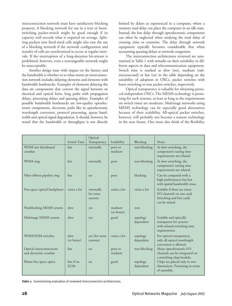
interconnection network must have satisfactory blockingproperty. A blocking network for use in a true or burst-switching packet-switch might be good enough if itscapacity well exceeds what is required on average. Split-ting packets into fixed-sized cells might also ease the useof a blocking network if the network configuration andtransfer of cells are synchronized to occur at regular inter-vals. If the interruption of a long-duration bit-stream isprohibited, however, even a rearrangeable network mightbe unacceptable.
Another design issue with impact on the latency andthe bandwidth is whether or to what extent an interconnec-tion network includes delaying elements and elements withbandwidth bottlenecks. Examples of elements delaying thedata are components that convert the signal between anelectrical and optical form, long paths with propagationdelays, processing delays and queuing delays. Examples ofpossible bandwidth bottlenecks are low-quality optoelec-tronic components, electronic paths like in optoelectronicwavelength converters, protocol processing, queue band-width and optical signal degradation. It should, however, benoted that the bandwidth or throughput is not directly
limited by delays as experienced in a computer, where amemory read delay can place the computer in an idle state.Instead, the low delay through optoelectronic componentscan often be neglected when studying the total delay ofcrossing cities or countries. The delay through networkequipment typically becomes considerable first whenaccounting queuing delays at network congestion.
The interconnection architectures reviewed are sum-marized in Table 1 with remarks on their suitability in dif-ferent aspects in data and telecommunication equipment.Switch time is marked as slow (ms), medium (sub-microsecond) or fast (ns) in the table depending on thesuitability of adoption in OXCs, packet switches withburst switching or true packet switches, respectively.
Optical transparency is valuable for obtaining proto-col-independent OXCs. The MEMS technology is prom-ising for such systems, at least as long as the requirementson switch times are moderate. Multistage networks usingMEMS technology can be especially good alternativesbecause of their scalability. All-optical packet switches,however, will probably not become a mature technologyin the near future. One must also think of the flexibility
Optical Switch Time Transparency Scalability Blocking Notes
WDM star distributed fast internally poor to non-blocking At slow switching, the crossbar medium component’s tuning time
requirements are relaxed.
WDM ring fast internally poor non-blocking At slow switching, the component’s tuning time requirements are relaxed.
Fiber-ribbon pipeline ring fast no poor blocking Can be compared with a high performance bus but with spatial bandwidth reuse.
Free space optical backplanes varies a lot internally varies a lot varies a lot Scalable if there are many for some I/O channels on one card. systems Switching and line cards
can be mixed.
Nonblocking MEMS system slow yes medium non(or better)
Multistage MEMS system slow yes good topology Scalable and optically dependent transparent for systems
with relaxed switching time requirements.
WDM/SDM switches slow yes (for some varies a lot topology For optical transparency,(or better) systems) dependent only all-optical wavelength
conversion is allowed.Optical interconnections fast no poor to non-blocking Many optoelectronic I/O and electronic crossbar medium channels can be integrated on
a switching chip/module.Planar free space optics fast if no no good topology Chips are placed only in two
SLMs dependent dimensions. Promising in terms of assembly.
Table 1: Summarizing evaluation of reviewed interconnection architectures.
5138454 6/23/03 10:44 AM Page 28

Optical Networks Magazine July/August 2003 29
and power of electronic switches and of electronic proces-sors to control the switches.
Scalability is desirable to be able to build equipmentwith many in/output ports. We state the scalability aspoor if only tens of ports are realistic, medium forhundred to a few hundred ports and good for a thousandports or more. Different multistage networks and freespace optical backplanes with a high density of opticalchannels seem to be good candidates from a scalabilitypoint of view. When building smaller systems instead theWDM star distributed crossbar with its passive opticalstar can be a good and simple alternative.
If an interconnection network implements a truecrossbar (like the WDM star distributed crossbar) it isnon-blocking, while whether a network is blocking ornon-blocking is topology dependent for many of thearchitectures reviewed. It should however be noted thatthe fiber-ribbon pipeline ring network is blocking. Onthe other hand, the increasingly good price/performanceratio for fiber-ribbon links indicates a great success poten-tial for interconnection systems using fiber-ribbon links.
It might be possible to build larger switch-fabricswith high transmission capacities using optics inside aswitch. The suitability of the different free space systemsdepends a great deal on the more detailed configurationsof the systems. For example, planar free space systems canbe arranged in arbitrary topologies.
Integrated fiber and waveguide solutions makepossible the building of compact systems, especially fornetworks that use fiber-ribbons. The same reasoning aboutcompactness can be argued for free space systems. Opticalbackplanes may earn their success from their similaritieswith current rack-based systems, while future planar free-space systems might give the possibility to integrate opticsand electronics in a compact and easy to assemble way.
For a more application-oriented comparison, Table 2summarizes about the suitability of the different intercon-nection architectures for OXCs, packet switches withburst switching and true packet switches. The switchtimes of the different interconnection networks havethe largest influence on this suitability. In addition to thepure interconnection demands, one must consider how
Packet switchesOXCs with burst switching True packet-switches
WDM star distributed Not suitable when optical Good for moderate Good for moderate numbercrossbar transparency is needed number of ports of ports if tuning time is low
WDM ring Not suitable when optical Good for small number Good for small number oftransparency is needed of ports ports if tuning time is low
Fiber-ribbon pipeline ring Not suitable when optical Good for small systems if Good for small systemstransparency is needed capacity is enough to deal if capacity is enough to deal
with blocking with blocking
Free space optical backplanes A passive optical backplane Passive backplanes can connect Passive backplanes can connectcan connect other optical boards while smart-pixel based boards while smart-pixel basedcomponents placed on backplanes even can participate backplanes even can participateinserted boards in the routing decisions in the routing decisions
Nonblocking MEMS system 2D MEMS is good for small Not suitable because of Not suitable because ofsystems, while 3D MEMS long switch times long switch timescan support rather many ports
Multistage MEMS system High number of ports is Not suitable because of Not suitable because of longpossible, when power long switch times switch timesbudget is acceptable
WDM/SDM switches A wide area of solutions Typically not targeted for Typically not targeted forexists, where wavelength switching-times short enough switching-times shortrouting functionality often for burst switching enough for packet switchingis integrated
Optical interconnections Not suitable when optical Flexible solution for both Flexible solution for bothand electronic crossbar transparency is needed small systems (single crossbar) small systems (single crossbar)
and large systems (multistage and large systems (multistageor similar) or similar)
Planar free space optics Integration of reconfigurable Can interconnect electronic Can interconnect electronicall-optical devices must crossbars in desired pattern crossbars in desired patternbe investigated
Table 2: Application suitability remarks.
5138454 6/23/03 10:44 AM Page 29

30 Optical Networks Magazine July/August 2003
buffering and routing intelligence are included in the com-munication equipment. Such components or functionscan both be integrated into the interconnection fabric andat the entrances and exits of the fabric. A more detailedstudy of this is out of the scope of this paper, however.
8 SummaryIn this paper, we have surveyed a number of inter-
connection architectures and technologies for use ininterconnection fabrics in communication equipment.Some of the technologies can be used in OXCs, burst-switching packet-switches and true packet-switches,while a MEMS-based interconnection fabric is limited touse in an OXC because of its long switch-time. On theother hand, the MEMS technology offers a good choicewhen requiring optical transparency. In packet switchesinstead, including electronic crossbars or other electronicscan offer required intelligence and flexibility for protocolprocessing.
9 References[1] F. Callegati, A.C. Cankaya, Y. Xiong, and M. Vanden-
houte, “Design issues of optical IP routers for Internetbackbone applications,” IEEE CommunicationsMagazine, vol. 37, no. 12, pp. 124-128, Dec. 1999.
[2] J. S. Turner, “Terabit burst switching,” Journal ofHigh Speed Networks, vol. 8, no. 1, pp. 3-16, 1999.
[3] D. J. Blumenthal, A. Carena, L. Rau, V. Curri, S.Humphries, “WDM optical IP tag switching withpacket-rate wavelength conversion and subcarriermultiplexed addressing,” Optical Fiber Communica-tion Conference, OFC’99, pp. 162-164, 1999.
[4] H. J. Chao and T.-S. Wang, “An optical interconnec-tion network for terabit IP routers,” Journal of Light-wave Technology, vol. 18, no. 12, pp. 2095-2112, Dec. 2000.
[5] G. Hjálmtysson, J. Yates, S. Chaudhuri, A. Green-berg, “Smart routers–simple optics: an architecturefor the optical internet,” Journal of Lightwave Tech-nology, vol. 18, no. 12, pp. 1880-1891, Dec. 2000.
[6] T.-S. Wang and S. Dixit, “A scalable and highcapacity all-optical packet switch: design, analysis,and control,” Photonic Network Communications,vol. 3, no. 1/2, pp. 101-110, 2001.
[7] D. Chiaroni, B. Lavigne, L. Hamon, A. Jourdan,F. Dorgeuille, C. Janz, E. Grard, M. Renaud, R.Bauknecht, C. Graf, H.P Schneibel, and H. Melchior,“Experimental validation of an all-optical networkbased on 160 Gbit/s throughput packet switchingnodes,” Proc. 24th European Conference on OpticalCommunication, Madrid, Spain, Sept. 20-24, 1998,vol. 1, pp. 573-574.
[8] M. Jonsson, “Fiber-optic interconnection networksfor signal processing applications,” 4th Interna-tional Workshop on Embedded HPC Systems and
Applications (EHPC’99) held in conjunction with the13th International Parallel Processing Symposium &10th Symposium on Parallel and Distributed Process-ing (IPPS/SPDP ‘99), San Juan, Puerto Rico, Apr.16, 1999. Published in Lecture Notes in ComputerScience. vol. 1586, Springer Verlag, pp. 1374-1385,1999, ISBN 3-540-65831-9.
[9] M. M. Eshaghian, “Parallel algorithms for imageprocessing on OMC,” IEEE Transactions on Com-puters, vol. 40, no. 7, pp. 827-833, July 1991.
[10] F. E. Kiamilev, P. Marchand, A. V. Krishnamoorthy,S. C. Esener, and S. H. Lee, “Performance compar-ison between optoelectronic and VLSI multistageinterconnection networks,” Journal of Lightwave Tech-nology, vol. 9, no. 12, pp. 1674-1692, Dec. 1991.
[11] T. M. Pinkston and C. Kuznia, “Smart-pixel-basednetwork interface chip,” Applied Optics, vol. 36,no. 20, pp. 4871-4880, July 10, 1997.
[12] J. W. Goodman, F. I. Leonberger, S.-Y. Kung, andR. A. Athale, “Optical interconnections for VLSIsystems,” Proceedings of the IEEE, vol. 72, no. 7,pp. 850-866, July 1984.
[13] A. A. Sawchuk, B. K. Jenkins, C. S. Raghavendra,and A. Varma, “Optical crossbar networks,” Com-puter, vol. 20, no. 6, pp. 50-60, June 1987.
[14] A. W. Lohmann, W. Stork, and G. Stucke, “Opticalperfect shuffle,” Applied Optics, vol. 25, no. 10,pp. 1530-1531, May 15, 1986.
[15] J. W. Goodman, “Fan-in and fan-out with opticalinterconnections,” Optica Acta, vol. 32, no. 12,pp. 1489-1496, 1985.
[16] H. S. Hinton, “Architectural considerations for photonicswitching networks,” IEEE Journal of Selected Areas inCommunications, vol. 6, no. 7, pp. 1209-1226, 1988.
[17] http://www.velio.com/.[18] D. B. Schwartz, K. Y. Chun, N. Choi, D. Diaz,
S. Planer, G. Raskin, and S. G. Shook,“OPTOBUS™ I: performance of a 4 Gb/s opticalinterconnect,” Proc. Massively Parallel Processingusing Optical Interconnections (MPPOI’96), Maui,HI, USA, Oct. 27-29, 1996, pp. 256-263.
[19] C.-L. Jiang, D. J. Brown, E. H. Mueller, A. E. Plotts,E. Cornejo, S. O’Neill, A. J. Heiney, and B. H. Reysen,“LED based parallel optical links,” Proc. LEOS’95,San Francisco, CA, USA, Oct. 30-Nov. 2, 1995,vol. 1, pp. 224-225.
[20] F. A. P. Tooley, “Optically interconnected electronics– challanges and choices,” Proc. Massively ParallelProcessing using Optical Interconnections (MPPOI’96),Maui, HI, USA, Oct. 27-29, 1996, pp. 138-145.
[21] T. Kurokawa, S. Matso, T. Nakahara, K. Tateno,Y. Ohiso, A. Wakatsuki, and H. Tsuda, “Designapproaches for VCSEL’s and VCSEL-based smartpixels toward parallel optoelectronic processing sys-tems,” Applied Optics, vol. 37, no. 2, pp. 194-204,Jan. 10, 1998.
5138454 6/23/03 10:44 AM Page 30

Optical Networks Magazine July/August 2003 31
[22] A. P. Kanjamala and A. F. J. Levi, “Sub-picosecondskew in multimode fiber ribbon for synchronousdata transmission,” Electronics Letters, vol. 31,pp. 1376-1377, 1995.
[23] Y.-M. Wong et al., “Technology development of ahigh-density 32-channel 16-Gb/s optical datalink for optical interconnection applications forthe optoelectronic technology consortium(OETC),” Journal of Lightwave Technology, vol.13, no. 6, pp. 995-1016, June 1995.
[24] T. Yoshikawa, S. Araki, K. Miyoshi, Y. Suemura,N. Henmi, T. Nagahori, H. Matsuoka, and T. Yokota,“Skewless optical data-link subsystem for massivelyparallel processors using 8 Gb/s � 1.1 Gb/s MMFarray optical module,” IEEE Photonics Technology Let-ters,” vol. 9, no. 12, pp. 1625-1627, Dec. 1997.
[25] N. Fujimoto, A. Ishizuka, H. Rokugawa, and K. Mori,“Skew-free parallel optical transmission systems,”Journal of Lightwave Technology, vol. 16, no. 10,pp. 1822-1831, Oct. 1998.
[26] K. Kasahara, “Optical interconnects speed up net-works,” Photonics Spectra, vol. 32, no. 2, pp. 127-128,1998.
[27] http://www.teraconnect.com/.[28] http://www.xanoptix.com/.[29] Y. Li, H. Kosaka, T. Wang, S. Kawai, and K. Kasa-
hara, “Applications of fiber image guides to bit-par-allel optical interconnections,” Optical Computing,vol. 10, 1995 OSA Technical Digest Series, Salt LakeCity, Utah, Mar. 13–16, 1995, pp. 286-288.
[30] Y. Li, T. Wang, and S. Kawai, “Distributed crossbarinterconnects with vertical-cavity surface-emittinglaser-angle multiplexing and fiber image guides,”Applied Optics, vol. 37, no. 2, pp. 254-263, Jan. 10,1998.
[31] D. V. Plant, M. B. Venditti, E. Laprise, J. Faucher,K. Razavi, M. Châteauneuf, A. G. Kirk, andJ. S. Ahearn, “256-channel bidirectional opticalinterconnect using VCSELs and photodiodes onCMOS,” Journal of Lightwave Technology, vol. 19,no. 8, pp. 1093-1103, Aug. 2001.
[32] M. L. Loeb and G. R. Stilwell, “High-speed datatransmission on an optical fiber using a byte-wideWDM system,” Journal of Lightwave Technology,vol. 6, no. 8, pp. 1306-1311, Aug. 1988.
[33] G. Jeong and J. W. Goodman, “Long-distanceparallel data link using WDM transmission withbit-skew compensation,” Journal of Lightwave Tech-nology, vol. 14, no. 5, pp. 655-660, May 1996.
[34] L. Bergman, J. Morookian, and C. Yeh, “An all-opticallong-distance multi-Gbytes/s bit-parallel WDMsingle-fiber link,” Journal of Lightwave Technology, vol.16, no. 9, pp. 1577-1582, Sept. 1998.
[35] L. A. Coldren, E. R. Hegblom, Y. A. Akulova, J. Ko,E. M. Strzelecka, and S. Y. Hu, “Vertical-cavitylasers for parallel optical interconnects,” Proc. 5th
International Conference on Massively Parallel Process-ing using Optical Interconnections (MPPOI’98), LasVegas, NV, USA, June 15-17, 1998, pp. 2-10.
[36] L. B. Aronson, B. E. Lemoff, L. A. Buckman, andD. W. Dolfi, “Low-cost multimode WDM for localarea networks up to 10 Gb/s,” IEEE PhotonicsTechnology Letters,” vol. 10, no. 10, pp. 1489-1491,Oct. 1998.
[37] M. Jonsson, A. Åhlander, M. Taveniku, andB. Svensson, “Time-deterministic WDM starnetwork for massively parallel computing in radarsystems,” Proc. Massively Parallel Processing usingOptical Interconnections (MPPOI’96), Maui, HI,USA, Oct. 27-29, 1996, pp. 85-93.
[38] K. Y. Eng, “A photonic knockout switch for high-speed packet networks,” IEEE Journal on Selected Areasin Communications, vol. 6, no. 7, pp. 1107-1116, Aug. 1988.
[39] C. A. Brackett, “On the capacity of multiwave-length optical-star packet switches,” IEEE LTS,pp. 33-37, May 1991.
[40] B. Li, Y. Qin, X.-R. Cao, and K. M. Sivalingam,“Photonic packet switching: architectures andperformance,” Optical Networks Magazine, vol. 2,no. 1, pp. 27-39, Jan./Feb. 2001.
[41] D. Sadot and I. Elhanany, “Optical switchingspeed requirements for Terabit/second packet overWDM networks,” IEEE Photonics Technology Let-ters,” vol. 12, no. 4, pp. 440-442, Apr. 2000.
[42] H. Kobrinski, M. P. Vecchi, E. L. Goldstein, andR. M. Bulley, “Wavelength selection with nano-second switching times using distributed-feedbacklaser amplifiers,” Electronics Letters, vol. 24, no. 15,pp. 969-971, July 21, 1988.
[43] K.-W. Cheung, “Acoustooptic tunable filters innarrowband WDM networks: system issues andnetwork applications,” IEEE Journal on SelectedAreas in Communications, vol. 8, no. 6, pp. 1015-1025, Aug. 1990.
[44] B. Mukherjee, “WDM-based local lightwave net-works part II: multihop systems,” IEEE Network,pp. 20-32, July 1992.
[45] A. S. Acampora and M. J. Karol, “An overview oflightwave packet networks,” IEEE Network,pp. 29-41, Jan. 1989.
[46] M. I. Irshid and M. Kavehrad, “A fully transparentfiber-optic ring architecture for WDM networks,”Journal of Lightwave Technology, vol. 10, no. 1,pp. 101-108, Jan. 1992.
[47] M. Maier and A. Wolisz, “Demonstrating thepotential of arrayed-waveguide grating based single-hop WDM networks,” Optical Networks Magazine,vol. 2, no. 5, pp. 75-85, Sept./Oct. 2001.
[48] Y. Sakai, “Full-mesh wavelength-routing WDMnetwork based on arrayed-waveguide grating,” Proc.LEOS’95, vol. 2, pp. 832-833, 2000.
5138454 6/23/03 10:44 AM Page 31

32 Optical Networks Magazine July/August 2003
[49] M. Jonsson, “Two fiber-ribbon ring networks forparallel and distributed computing systems,” OpticalEngineering, vol.37,no.12,pp.3196-3204,Dec.1998.
[50] B. Raghavan, Y.-G. Kim, T.-Y. Chuang, B. Madhavan,and A. F. J. Levi, “A Gbyte/s parallel fiber-opticnetwork interface for multimedia applications,”IEEE Network, vol. 13, no. 1, pp. 20-28, Jan./Feb.1999.
[51] B. J. Sano and A. F. J. Levi, “Networks for theprofessional campus environment,” in MultimediaTechnology for Applications. B. Sheu and M. Ismail,Eds., McGraw-Hill, Inc., pp. 413-427, 1998, ISBN0-7803-1174-4.
[52] B. Sano, B. Madhavan, and A. F. J. Levi, “8 GbpsCMOS interface for parallel fiber-optic intercon-nects,” Electronics Letters, vol. 32, pp. 2262-2263,1996.
[53] POLO Technical Summary. University of SouthernCalifornia, Oct. 1997.
[54] P. Eriksen, K. Gustafsson, M. Niburg, G. Palmskog,M. Robertsson, and K. Åkermark, “The Apollodemonstrator – new low-cost technologies for opticalinterconnects,” Ericsson Review, vol. 72, no. 2, 1995.
[55] M. Robertsson, K. Engberg, P. Eriksen, H.Hesselbom, M. Niburg, and G. Palmskog, “Opticalinterconnects in packaging for telecom applica-tions,” Proc. of the 10th European MicroelectronicsConference, pp. 580-591, 1995.
[56] M. A. Shahid and W. R. Holland, “Flexible opticalbackplane interconnections,” Proc. 3rd Interna-tional Conference on Massively Parallel Processingusing Optical Interconnections (MPPOI’96), Maui,HI, USA, Oct. 27-29, 1996, pp. 178-185.
[57] J. W. Parker, P. J. Ayliffe, T. V. Clapp, M. C. Geear,P. M. Harrison, and R. G. Peall, “Multifibre bus forrack-to-rack interconnects based on opto-hybridtransmitter/receiver array pair,” Electronics Letters,vol. 28, no. 8, pp. 801-803, April 9, 1992.
[58] P. Lukowicz, S. Sinzinger, K. Dunkel, andH. D. Bauer, “Design of an opto-electronic VLSI/parallel fiber bus,” Proc. Optics in Computing (OC’98),Brugge, Belgium, June 17-20, 1998, pp. 289-292.
[59] Y. Li, J. Popelek, J.-K. Rhee, L. J. Wang, T. Wang,and K. Shum, “Demonstration of fiber-based board-level optical clock distributions,” Proc. 5th Interna-tional Conference on Massively Parallel Processingusing Optical Interconnections (MPPOI’98), LasVegas, NV, USA, June 15-17, 1998, pp. 224-228.
[60] J. Jahns, “Planar packaging of free-space opticalinterconnects,” Proceedings of the IEEE, vol. 82, no.11, pp. 1623-1631, Nov. 1994.
[61] J. Jahns, “Integrated free-space optical intercon-nects for chip-to-chip communications,” Proc. 5thInternational Conference on Massively Parallel Pro-cessing using Optical Interconnections (MPPOI’98),Las Vegas, NV, USA, June 15–17, 1998, pp. 20-23.
[62] S. Reinhorn, R. Oron, Y. Amitai, A. A. Friesem,K. Vinokur, and N. Pilossof, “Planar opticaldynamic crossbar switch,” Optical Engineering, vol.38, no. 8, pp. 1396-1401, Aug. 1999.
[63] C. Zhao, T.-H. Oh, and R. T. Chen, “General pur-pose bidirectional optical backplane: high-perform-ance bus for multiprocessor systems,” Proc. 2ndInternational Conference on Massively Parallel Process-ing using Optical Interconnections (MPPOI’95), SanAntonio, TX, USA, Oct 23-24, 1995, pp. 188-195.
[64] C. Zhao, J. Liu, and R. T. Chen, “Hybrid optoelec-tronic backplane bus for multiprocessor-based com-puting systems,” Proc. 3rd International Conferenceon Massively Parallel Processing using Optical Inter-connections (MPPOI’96), Maui, HI, USA, Oct.27-29, 1996, pp. 313-320.
[65] T. H. Szymanski, “Intelligent optical backplanes,”Optical Computing, vol. 10, 1995 OSA TechnicalDigest Series, Salt Lake City, Utah, Mar. 13-16,1995, pp. 11-13.
[66] B. Supmonchai and T. Szymanski, “High speedVLSI concentrators for terabit intelligent opticalbackplanes,” Proc. Optics in Computing (OC’98),Brugge, Belgium, June 17-20, 1998, pp. 306-310.
[67] T. Szymanski and H. S. Hinton, “Design of aterabit free-space photonic backplane for parallelcomputing,” Proc. 2nd International Conference onMassively Parallel Processing using Optical Intercon-nections (MPPOI’95), San Antonio, TX, USA, Oct23-24, 1995, pp. 16-27.
[68] K. Hirabayashi, T. Yamamoto, and S. Hino,“Optical backplane with free-space optical intercon-nections using tunable beam deflectors and a mirrorfor bookshelf-assembled terabit per second classasynchronous transfer mode switch,” Optical Engi-neering, vol. 37, no. 4, pp. 1332–1342, Apr. 1998.
[69] K. Hamanaka, “Otical bus interconnection systemusing selfloc lenses,” Optics Letters, vol. 16, no. 6,pp. 1222-1224, Aug. 15, 1991.
[70] T. H. Szymanski, A. Au, M. Lafrenière-Roula,V. Tyan, B. Supmonchai, J. Wong, B. Zerrouk, andS. T. Obenaus, “Terabit optical local area networksfor multiprocessing systems,” Applied Optics, vol.37, no. 2, pp. 264-275, Jan. 10, 1998.
[71] A. V. Krisnamoorthy et al., “The AMOEBA chip:an optoelectronic switch for multiprocessor net-working using dense-WDM,” Proc. 3rd Interna-tional Conference on Massively Parallel Processingusing Optical Interconnections (MPPOI’96), Maui,HI, USA, Oct. 27-29, 1996, pp. 94-100.
[72] S. Nishimura, T. Kudoh, H. Nishi, J. Yamamoto,K. Harasawa, N. Matsudaira, S. Akutsu, andH. Amano, “64-Gb/s highly reliable networkswitch (RHiNET-2/SW) using parallel opticalinterconnection,” Journal of Lightwave Technology,vol. 18, no. 12, pp. 1620-1627, Dec. 2000.
5138454 6/23/03 10:44 AM Page 32

Optical Networks Magazine July/August 2003 33
[73] F. B. McGormick et al., “Five-stage free-space opticalswitching network with field-effect transistor self-electro-optic-effect-device smart-pixel arrays,” AppliedOptics, vol. 33, no. 8, pp. 1601-1618, Mar. 1994.
[74] T. J. Cloonan, “Comparative study of opticalinterconnection technologies for large asynchronoustransfer mode packet switching applications,” Opt-ical Engineering, vol. 33, no. 5, pp. 1512–1523,May 1994.
[75] T. Goh, M. Yasu, K. Hattori, A. Himeno,M. Okuno, and Y. Ohmori, “Low-loss and high-extinction-ratio silica-based strictly nonblocking16 � 16 thermooptic matrix switch,” IEEE Photon-ics Technology Letters,” vol. 10, no. 6, pp. 810-812,June 1998.
[76] D. A. B. Miller, D. S. Chemla, T. C. Damen,A. C. Gossard, W. Wiegmann, T. H. Wood, andC. A. Burrus, “Novel hybrid optically bistableswitch: the quantum well self-electro-optic effectdevice,” Applied Physics Letters,” vol. 45, no. 1,pp. 13-15, July 1, 1984.
[77] T. Kato, J. Sasaki, T. Shimoda, H. Hatakeyama,T. Tamanuki, M. Yamaguchi, M. Kitamura, andM. Itoh, “10 Gb/s photonic cell switching withhybrid 4 � 4 optical matrix switch module on silicabased planar waveguide platform,” Optical FiberCommunication Conference, OFC’98 Technical Di-gest, San Jose, CA, USA, Feb. 22–27, 1998, pp.437–440.
[78] R. J. S. Pedersen, B. Mikkelsen, B. F. Jørgensen, M.Nissov, K. E. Stubkjaer, K. Wünstel, K. Daub, E.Lach, G. Laube, W. Idler, M. Schilling, P. Doussiere,and F. Pommerau, “WDM cross-connect cascadebased on all-optical wavelength converters for rout-ing and wavelength slot interchanging using areduced number of internal wavelengths,” OpticalFiber Communication Conference, OFC’98 TechnicalDigest, San Jose, CA, USA, Feb. 22-27, 1998,pp. 58-59.
[79] R. Flipse, “Optical switches ease bandwidth crunch,”EuroPhotonics, vol. 3, no. 5, pp. 44-45, Aug./Sept.1998.
[80] J. H. Reif and A. Yoshida, “Free space opticalmessage routing for high performance parallelcomputers,” Proc. Massively Parallel Processing usingOptical Interconnections (MPPOI’94), Cancun,Mexico, Apr. 26-27, 1994, pp. 37-44.
[81] R. D. Chamberlain, M. A. Franklin, R. B. Krch-navek, and B. H. Baysal, “Design of an optically-interconnected multiprocessor,” Proc. 5th Interna-tional Conference on Massively Parallel Processing usingOptical Interconnections (MPPOI’98), Las Vegas, NV,USA, June 15-17, 1998, pp. 114-122.
[82] C. S. Baw, R. D. Chamberlain, M. A. Franklin, andM. G. Wrighton, “The Gemini interconnect: datapath measurements and performance analysis,” Proc.
6th International Conference on Parallel Interconnects(PI’99), pp. 21-30, 1999.
[83] P. Granestrand, B. Stoltz, L. Thylen, K. Bergvall,W. Döldissen, H. Heinrich, and D. Hoffmann,“Strictly nonblocking 8 x 8 integrated optical switchmatrix,” Electronics Letters, vol. 22, no. 15, pp. 816-818, July 17, 1986.
[84] S. Kawai, H. Kurita, and K. Kubota, “Design ofelectro-photonic computer-networks with non-blocking and self-routing functions,” Optical Com-puting, vol. 10, 1995 OSA Technical Digest Series, SaltLake City, Utah, Mar. 13-16, 1995, pp. 263-265.
[85] M. P. Christensen and M. W. Haney, “Two-bouncefree-space arbitrary interconnection architecture,”Proc. Massively Parallel Processing using OpticalInterconnections (MPPOI’97), Montreal, Canada,June 22-24, 1997, pp. 61-67.
[86] C. Duan and C. W. Wilmsen, “OptoelectronicATM switch using VCSEL and smart detectorarrays,” Proc. Optics in Computing (OC’98), Brugge,Belgium, June 17-20, 1998, pp. 103-106.
[87] A. Tajima, N. Kitamura, S. Takahashi, S. Kitamura,Y. Maeno, Y. Suemura, and N. Henmi, “10-Gb/s/port gated divider passive combiner optical switchwith single-mode-to-multimode combiner,” IEEEPhotonics Technology Letters,” vol. 10, no. 1, pp. 162-164, Jan. 1998.
[88] Y. Maeno, A. Tajima, Y. Suemura, and N. Henmi,“8.5 Gbit/s/port synchronous optical packet-switch,”Proc. Massively Parallel Processing using Optical Inter-connections (MPPOI’97), Montreal, Canada, June22-24, 1997, pp. 114-119.
[89] A. Neukermans and R. Ramaswami, “MEMS tech-nology for optical networking applications,” IEEECommunications Magazine, vol. 39, no. 1, pp. 62-69,Jan. 2001.
[90] L. Y. Lin, “Free-space micromachined optical-switching technologies and architectures,” OpticalFiber Communication Conference, OFC’99, vol. 2,pp. 154-156, 1999.
[91] C. Pu, L. Y. Lin, E. L. Goldstein, and R. W. Tkach,“Client-configurable eight-channel optical add/dropmultiplexer using micromachining technology,”IEEE Photonics Technology Letters,” vol. 12, no. 12,pp. 1665, Dec. 2000.
[92] M. Kenward, “Mirror magic ushers in the allopticalnetwork,” Fibre Systems, pp. 37-39, May 2000.
[93] G. Shen, T. H. Cheng, S. K. Bose, C. Lu,and T. Y. Chai, “Architectural design for multi-stage 2-D MEMS optical switches,” Journal ofLightwave Technology, vol. 20, no. 2, pp. 178-187,Feb. 2002.
[94] A. Pattavina, M. Martinelli, G. Maier, and P. Boffi,“Techniques and technologies towards all-opticalswitching,” Optical Networks Magazine, vol. 1, no.2, pp. 75-93, Apr. 2000.
5138454 6/23/03 10:44 AM Page 33

34 Optical Networks Magazine July/August 2003
Magnus [email protected] Jonsson received his B.S. and M.S.degrees in computer engineering fromHalmstad University, Sweden, in 1993and 1994, respectively. He then obtainedthe Licentiate of Technology and Ph.D.degrees in computer engineering fromChalmers University of Technology, Gothenburg, Sweden, in 1997and 1999, respectively. From 1998 to March 2003, he was AssociateProfessor of Data Communication at Halmstad University (acting
between 1998 and 2000). Since April 2003, he has been Professor ofReal-Time Computer Systems at Halmstad University. He has pub-lished about 35 scientific papers, most of them in the area of opticalcommunication and real-time communication. Most of his research istargeted for embedded, industrial and parallel and distributedcomputing and communication systems. Dr. Jonsson has served on theprogram committees of International Workshop on Optical Networks,IEEE International Workshop on Factory Communication Systems,International Conference on Computer Science and Informatics, andInternational Workshop on Embedded/Distributed HPC Systemsand Applications.
5138454 6/23/03 10:44 AM Page 34