optics and quantum optics with semiconductor...
TRANSCRIPT

Optics and Quantum Optics with Semiconductor Nanostructures
Stephan W. Koch Department of Physics, Philipps University, Marburg/Germany
andOptical Sciences Center, University of Arizona, Tucson/AZ
theory: Kira, Hoyer et al., MarburgHader, Moloney et al., Tucson
experiments: Gibbs/Khitrova et al., Tucson,Stolz et al., Rostock
• background: optics with atoms• semiclassical semiconductor optics • semiconductor quantum optics:
“which way” experiments and light – matter entanglement
Overview
Collaborators

Marburg

You do not really understand something unless you can explain it to your grandmother (Albert Einstein)
Marburg

atom
43
2
n=1
From Atoms to Solids …
optical absorption/emission =transitions between atomic levels

atom
unit cell
solid
(2 - 5) * 10-8cm
energy states
bands
43
2
n=1
From Atoms to Solids …

possible energy values of electrons in crystal
intrinsic semiconductor:full valence band(s),empty conduction band
E
kEg
Bandstructure

6
4
2
0
-2
-4
-6
-8
-10
-12
L XΓ
Ene
rgy
(eV
)
Realistic Bandstructure GaAs
effective mass approximation
often: photon momentum typical carrier momentum � perpendicular transitions,

Energy Gap in Semiconductors
gap energy determines frequency and therefore color (wavelength) of absorbed and/or emitted light
1ω� 2ω�
conduction band
valence band

������������� ���������� ������� ����
������������ ��������������

Bandgaps of III-V Alloys (300 K)
5.4 5.6 5.8 6.0 6.2 6.4 6.60.0
0.5
1.0
1.5
2.0
2.5
lattice constant (Angstrom)
Ene
rgy
gap
(eV
)
wav
elen
gth
(mic
ron)
1.00
2.0
AlSb
5.010.0
GaP
GaAs
AlAs
InP
InAs
GaSb
InSb
0.620
0.517
0.775
1.55

Quasi-Two Dimensional Structure
discrete states (z direction) and continuous bands (x-y plane)
TEM picture: quantum well structure
band gap at Γ-point (direct semiconductor)

self organizedquantum dots
Semiconductors as Designer Materials
� quantum well = two-dimensional electronic mobility
� quantum wire = one-dimensional electronic mobility
� quantum dot = no (zero-dimensional) electronic mobility

Interband Light-Matter Interaction:Semiclassical Theory
semiconductor:Bloch basis
classical Maxwell’s wave equation macroscopicoptical polarization
Coulomb interaction of chargecarriers quantum mechanical
many-body problem ofinteracting Fermions
→

Semiconductor Bloch Equations (SBE)
• nonlinearities: phase space fillinging, gap renormalization,Coulomb attraction
• correlation effects: scattering, dephasing, screening, …
field renormalization
energy renormalization

Wannier Excitons
• 2 parabolic bandselectron-hole pairinterband Coulombattraction
• wavefunction
• relative motion(Wannier equation)
• hydrogen atom like solutions, Wannier excitons = quasi atoms (finite lifetime < nanoseconds)
c
v
Coulomb potential

Wannier Excitons
• linear absorption Elliott formula
• linear optics: excitonic resonances• INTERACTION induced resonances, not just transitions between bands

Exciton Saturation
F. Jahnke, M. Kira, and S.W. Koch, Z. Physik B 104, 559 (1997)Born-Markov approximation
Detuning
saturation via excitation induced dephasing (EID)= Coulomb induced destructive interference
between different

Exciton Saturation
F. Jahnke, M. Kira, and S.W. Koch, Z. Physik B 104, 559 (1997)
Detuning
Abs
orpt
ion
• experiment: InGaAs/GaAs QW• Khitrova, Gibbs, Jahnke, Kira, Koch, Rev. Mod. Phys. 71, 1591 (1999)• EID first observed in 4-wave mixing, Wang et al. PRL 71, 1261 (1993)

Lineshape Problem
0.2
0.0
-0.4
-0.2
-0.6 -20 -10 0 10
Detuning
Abs
orpt
ion
[103 /
cm]
full calculation
dephasing rate approximation
•
• gain of two-band bulk material
• nondiagonal scattering contributions → lineshape modification,no absorption below the gap

abso
rptio
n (x
103 /
cm)
abso
rptio
n/ga
in [1
/cm
]
abso
rptio
n/ga
in
Photon Energy (eV)
Current 0-20mA… Density 0.6-3.0x1012cm-2
exp: C. Ellmers et al., theory: A. Girndt et al. MarburgCourtesy of W.W. Chow, P.M. Smowton, P. Blood, A. Grindt, F. Jahnke, and S.W. Koch
8nm InGaAs/AlGaAs 6.8 nm In0.4Ga0.5P/(Al0.5Ga0.5)In0.51P0.49
10nm (9.2nm) InGaAs/AlGaAs
N=1.6, 2.2, 2.5, 3.0*1012/cm2
exp: D. Bossert et al., theory: A. Girndt et al., Marburg
Detuning
Detuning
Optical Gain in Semiconductors: Theory and Experiment

• quantitative understanding of interaction phenomena• strong experiment – theory interactions• predictive capability of theory
CHALLENGES:
• modified photonic environment (nano optics with nano structures)• optimized design for specific applications• nonequilibrium phenomena ….
Selected References:
• Haug/Koch, “Quantum Theory of the Optical and Electronic Properties of Semiconductors” 4th ed., World Scientific Publ. (2004)
• Khitrova et al., Rev. Mod. Phys. 71, 1591 (1999)
Summary of Semiclassical Phenomena

Quantized Light-Matter Interaction
where is proportional to dipole matrix element and mode strength at the QW position
Kira et al., Prog. Quantum. Electron. 23, 189 (1999)

Spontaneous Emission from Quantum Wells
-|q |z+|q |z
+-
recombination in electron-hole system
emission occurs simultaneously to left and right, i.e. with and
no translational invariance perpendicular to QW
no momentum conservation

Non Resonantly Excited Photoluminescence
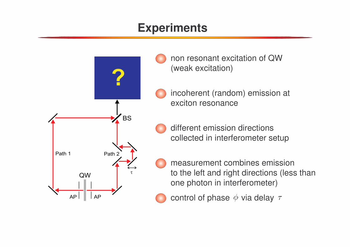
Experiments
t
QW
BS
AP AP
Path 2Path 1
?
non resonant excitation of QW (weak excitation)
incoherent (random) emission at exciton resonance
different emission directions collected in interferometer setup
measurement combines emission to the left and right directions (less thanone photon in interferometer)
control of phase via delay

Experiments (I)
t
QW
BS
AP AP
Path 2Path 1
QW perpendicular

Experiments (II)
t
QW
BS
AP AP
Path 2Path 1
?QW tilted

Experiments (II)
t
QW
BS
AP AP
Path 2Path 1
QW tilted

Experiments (III)
0 20 40 60 80 100
-2 0 20.0
0.2
0.4
CCD pixels
PL
inte
nsity (
a.u
.)
t (ps)
Contr
astno tilt|
with tilt
single beamintensities
Oct. 2003
clear interferences visible if QW NOT tilted
interferences vanish if QW tilted
Hoyer et al. PRL 93, 067401 (2004)

Summary of Experimental Observations
interferences seen in incoherent (single photon) emission
, but intensity shows interferences
interference shows strong directional sensitivity

Summary of Experimental Observations
interferences seen in incoherent (single photon) emission
, but intensity shows interferences
interference shows strong directional sensitivity
effects predicted in Prog. Quantum. El. 23, 189 (1999)
origin of effects: light-matter entanglement & which-way interferences

Spontaneous Emission from Quantum Wells
-|q |z+|q |z
q||
+-
electron-hole recombination
simultaneous emission in and directions
photon emission with same
recoil momentum transferred to carrier system

CASE A: Emission with same
emission to the left
emission to the right
paths not distinguishable with respect to carrier system (i.e. no entanglement)
Explanation of Interferences (I)
q|| q||
photon
many-body wavefunction with recoil

Explanation of Interferences (II)
q|| q||
BL BR
variable phase
emission intensity IL to the left IR to the right interference
interferometry:
INTERFERENCE can be seen

Explanation of Entanglement (I)
CASE B: Emission with different
emission to the left
emission to the right
paths identified by entanglement
q|| q'||
photons
many-body wavefunction with recoil

Explanation of Entanglement (II)
q|| q'||
emission to the left (BL) und to the right (BR) is combined in detector D = BL +BR
emissions intensity IL to the left IR to the right interference
NO interference pattern due to entanglement

Theory of Entanglement-Interferences
semiconductor luminescence equations PRL 97, 5170 (1997)
photon-assisted correlations
photon correlations
in the presence of Coulomb interaction
QUESTION: WHAT HAPPENS IF WE TAKE MANY QUANTUM WELLS ?

Theory of Entanglement-Interferences
Predictions for n quantum wells with spacing d
perfect interferences for Bragg
no interferences for anti-Bragg (n-even)
0 1 2 3 4 5 6 7 8 9
Number of QWs
0.0
0.5
1.0
/4
/2
Prog. Quantum. El. , 189 (1999)23dI

Entanglement-Interference Experiment (IV)
interferences seen in multiple QW system with λ/2 spacing
interferences vanishin multiple QW system with λ/4 spacing
λ/4 spacing leads to complete randomizing of emission to the left and to the right
confirmation of theoretical predictions
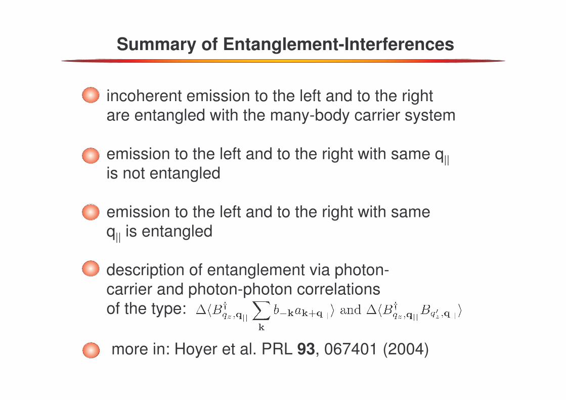
Summary of Entanglement-Interferences
incoherent emission to the left and to the right are entangled with the many-body carrier system
emission to the left and to the right with same q||is not entangled
emission to the left and to the right with sameq|| is entangled
description of entanglement via photon-carrier and photon-photon correlations of the type:
more in: Hoyer et al. PRL 93, 067401 (2004)

• variety of novel quantum optical effects in semiconductors• strong experiment – theory interactions
MANY CHALLENGES:
• optimization and application of non-classical properties (quantum information science, …)
• modified photonic environment (phot. x-tals, …)• role of incoherent excitons, biexcitons, ….
Selected References:
• Haug/Koch, “Quantum Theory of the Optical and Electronic Properties of Semiconductors” 4th ed., World Scientific Publ. (2004)
• Khitrova et al., Rev. Mod. Phys. 71, 1591 (1999)• Kira et al., Prog. Quantum. Electron. 23, 189 (1999)
Summary