optimization of a self-oscillating power converter for ... · such a self-oscillating circuit for...
TRANSCRIPT
IEEE PEDS 2017, Honolulu, USA
12 – 15 December 2017
978-1-5090-2364-6 /17/$31.00 ©2017 European Union
Optimization of a Self-Oscillating Power Converter
for Resonant Switching in a
Contactless Inductive Energy Transfer System
for Low Voltage Onboard Supply System
in Lightweight Construction Electric Vehicles
M. Böttigheimer, N. Parspour, S. Maier
Institut für Elektrische Energiewandlung (IEW)
Universität Stuttgart
Pfaffenwaldring 47, 70569 Stuttgart
Abstract-. In the future, mobility will be dominated by different forms of e-mobility. The related disadvantages such as the limited range could be compensated by automatic systems for
inductive charging. With highly automated and intelligent inductive charging systems, every parking and stopping process can be used to recharge the traction batteries without any
interaction of the driver. For e-vehicles smaller than the size class of electric passenger vehicles, as here for instance an electric go-kart, generally low voltage batteries (instead of high
voltage batteries) are used. Hence, different standards are required for charging systems for these low voltage batteries, as for example a lower voltage drop on the secondary side and a
simple technical implementation. One possible approach is the use of a high-power oscillator on the primary side in combination with a double-sided parallel compensation. A
system like this, just due to circuit state, safe operates by principle in terms of open circuit and short circuit stability. If the windings are taken away from one another, the power
transfer performance decreases in proportion to the coupling factor down to zero, only because of the circuit state. Therefore, monitoring system is not necessary. In this paper, the optimal
design of the parallel compensated charging system for a charging power of 1 kW with a 60 V traction battery is presented, as well as the optimization of the high-power
oscillator for high efficiency and the avoidance of EMI-relevant switching interference.
I. INTRODUCTION
For the contactless energy transfer (CET), it is necessary to
switch resonantly or quasi-resonantly in order to operate
nearly lossless. The CET-system can have an external control
signal. Under specific circumstances, also a self-oscillating
CET-system without an external control signal can be used as
well. The first designs of self-oscillating circuits are from
Meißner [1] and Armstrong [2] and have been further
developed by Royer [3, 4] and Rehrmann [5]. In this paper,
such a self-oscillating circuit for the special boundary
conditions of the CET is being examined and optimized for
its implementation in CET for low voltage up to 60 V and an
operating frequency of 50 kHz. A future application in the
low-power sector of up to approximately 1 kW is then
possible [6]. The hereby examined double-sided Royer-
converter with a double-sided parallel compensation, is
especially suitable for lightweight vehicles with low power
(up to approx. 1 kW) [6], whereas the double-sided serial
compensation is very useful for a power range of 3 to 20 kW
[7], [8].
II. TRANSFER TOPOLOGY AND THE APPLICATION OF A
ROYER-CONVERTER
A. Contactless Energy Transfer With a Double-Sided Parallel
Compensation
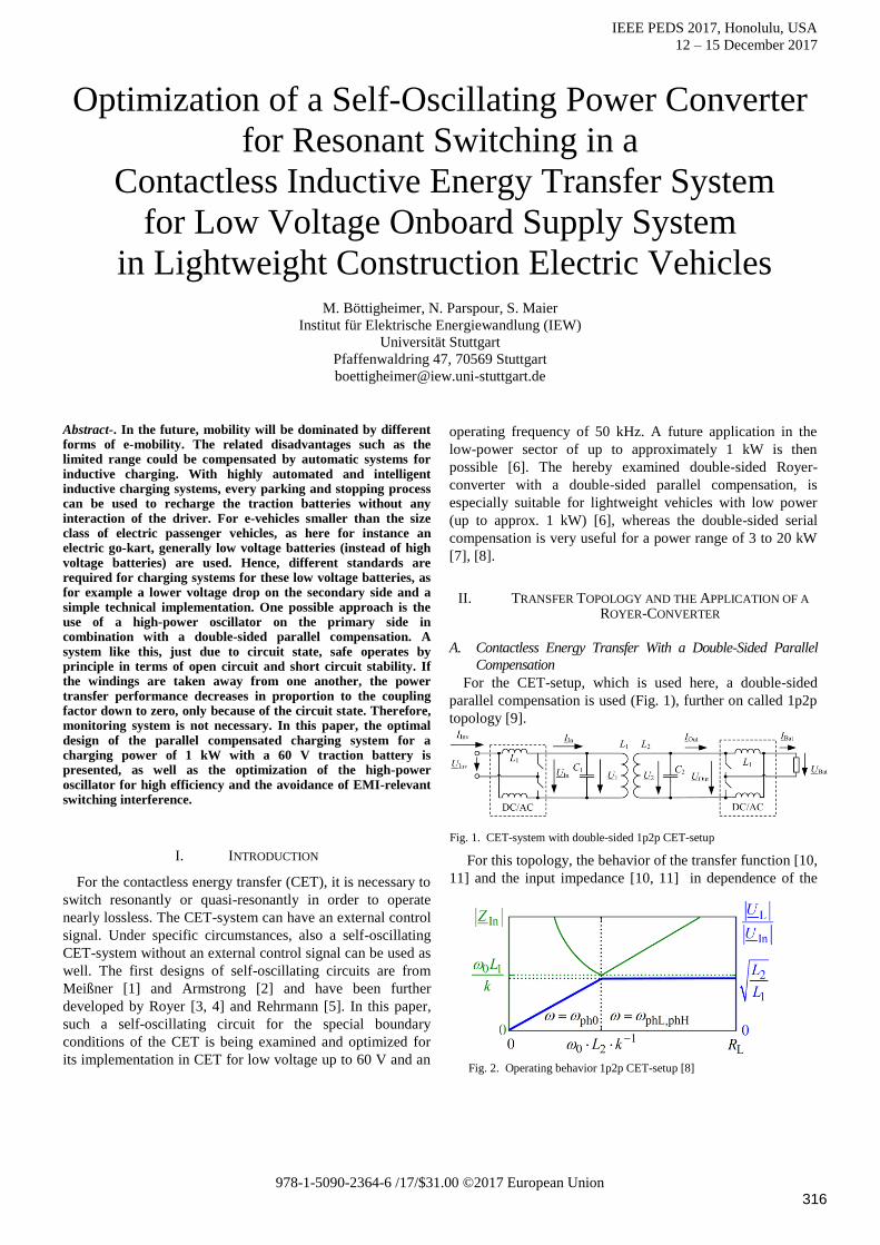
For the CET-setup, which is used here, a double-sided
parallel compensation is used (Fig. 1), further on called 1p2p
topology [9].
For this topology, the behavior of the transfer function [10,
11] and the input impedance [10, 11] in dependence of the
Fig. 1. CET-system with double-sided 1p2p CET-setup
Fig. 2. Operating behavior 1p2p CET-setup [8]
316
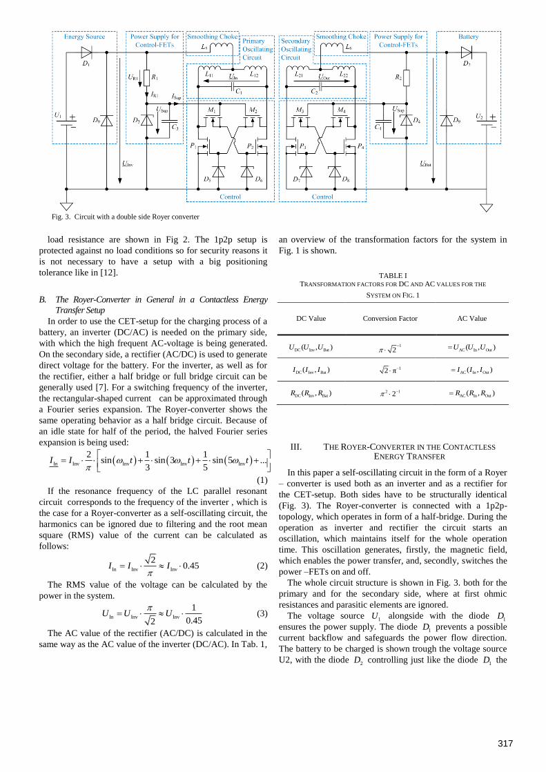
load resistance are shown in Fig 2. The 1p2p setup is
protected against no load conditions so for security reasons it
is not necessary to have a setup with a big positioning
tolerance like in [12].
B. The Royer-Converter in General in a Contactless Energy
Transfer Setup
In order to use the CET-setup for the charging process of a
battery, an inverter (DC/AC) is needed on the primary side,
with which the high frequent AC-voltage is being generated.
On the secondary side, a rectifier (AC/DC) is used to generate
direct voltage for the battery. For the inverter, as well as for
the rectifier, either a half bridge or full bridge circuit can be
generally used [7]. For a switching frequency of the inverter,
the rectangular-shaped current can be approximated through
a Fourier series expansion. The Royer-converter shows the
same operating behavior as a half bridge circuit. Because of
an idle state for half of the period, the halved Fourier series
expansion is being used:
In Inv Inv Inv Inv
2 1 1sin sin 3 sin 5 ...
3 5I I t t t
(1)
If the resonance frequency of the LC parallel resonant
circuit corresponds to the frequency of the inverter , which is
the case for a Royer-converter as a self-oscillating circuit, the
harmonics can be ignored due to filtering and the root mean
square (RMS) value of the current can be calculated as
follows:
In Inv Inv
20.45I I I
(2)
The RMS value of the voltage can be calculated by the
power in the system.
In Inv Inv
1
0.452U U U
(3)
The AC value of the rectifier (AC/DC) is calculated in the
same way as the AC value of the inverter (DC/AC). In Tab. 1,
an overview of the transformation factors for the system in
Fig. 1 is shown.
TABLE I TRANSFORMATION FACTORS FOR DC AND AC VALUES FOR THE
SYSTEM ON FIG. 1
DC Value Conversion Factor AC Value
DC Inv Bat( , )U U U 1
2
AC In Out( , )U U U
DC Inv Bat( , )I I I 12 π AC In Out( , )I I I
DC Inv Bat( , )R R R 2 12 AC In Out( , )R R R
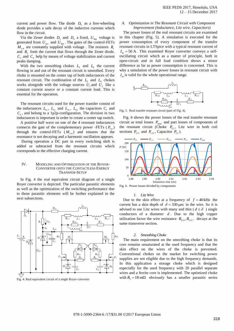
III. THE ROYER-CONVERTER IN THE CONTACTLESS
ENERGY TRANSFER
In this paper a self-oscillating circuit in the form of a Royer
– converter is used both as an inverter and as a rectifier for
the CET-setup. Both sides have to be structurally identical
(Fig. 3). The Royer-converter is connected with a 1p2p-
topology, which operates in form of a half-bridge. During the
operation as inverter and rectifier the circuit starts an
oscillation, which maintains itself for the whole operation
time. This oscillation generates, firstly, the magnetic field,
which enables the power transfer, and, secondly, switches the
power –FETs on and off.
The whole circuit structure is shown in Fig. 3. both for the
primary and for the secondary side, where at first ohmic
resistances and parasitic elements are ignored.
The voltage source 1U alongside with the diode
1D
ensures the power supply. The diode 1D prevents a possible
current backflow and safeguards the power flow direction.
The battery to be charged is shown trough the voltage source
U2, with the diode 2D controlling just like the diode
1D the
Fig. 3. Circuit with a double side Royer converter
317
IEEE PEDS 2017, Honolulu, USA
12 – 15 December 2017
978-1-5090-2364-6 /17/$31.00 ©2017 European Union
current and power flow. The diode 9D as a free-wheeling
diode provides a safe decay of the inductive currents which
flow in the circuit.
Via the Zener diodes 3D and
4D a fixed, BatU voltage is
generated from InvU and
BatU . The gates of the control-FETs
1-4M are constantly supplied with voltage . The resistors 1R
and 2R limit the current that flows through the Zener diode.
3C and 4C help by means of voltage stabilization and current
peaks damping.
With the two smoothing chokes 5L and
6L the current
flowing in and out of the resonant circuit is smoothed. Every
choke is mounted on the center tap of both inductances of the
resonant circuit. The combination of the 5L and
6L chokes
works alongside with the voltage sources 1U and
2U like a
constant current source or a constant current load. This is
essential for the operation.
The resonant circuits used for the power transfer consist of
the inductances 11L ,
12L and 21L ,
22L the capacitors 1C and
2C , and belong to a 1p2p-configuration. The division in two
inductances is important in order to create a center tap switch.
A positive half wave on one of the 4 resonant inductances
connects the gate of the complementary power -FETs (1-4P )
through the control-FETs (1-4M ) and ensures that the
resonance is not decaying and a harmonic oscillation appears.
During operation a DC part in every switching shift is
added or subtracted from the resonant circuits which
corresponds to the effective charging current.
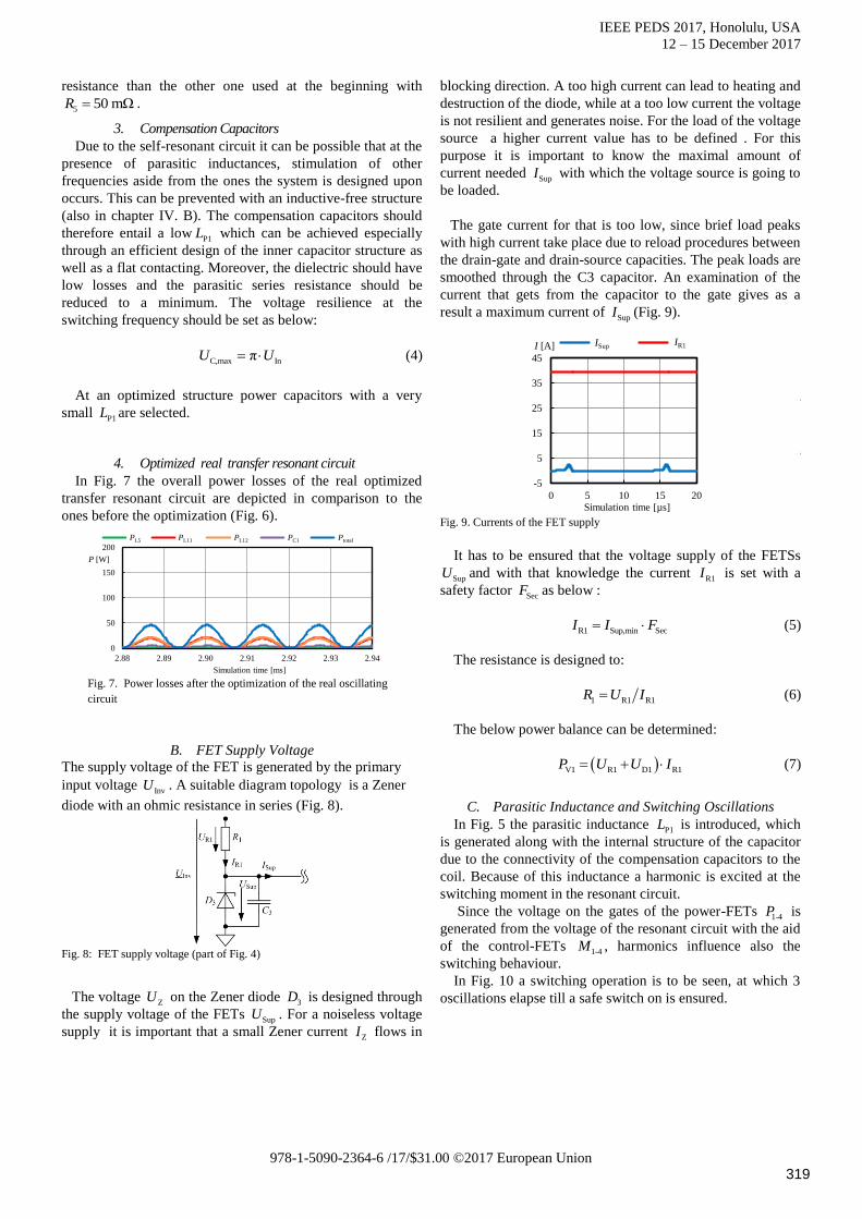
IV. MODELING AND OPTIMIZATION OF THE ROYER-CONVERTER ONTO THE CONTACTLESS ENERGY
TRANSFER-SETUP
In Fig. 4 the real equivalent circuit diagram of a single
Royer converter is depicted. The particular parasitic elements
as well as the optimization of the switching performance due
to those parasitic elements will be further explained in the
next subsections.
A. Optimization in The Resonant Circuit with Component
Improvement (Inductance, Litz wire, Capacitors)
The power losses of the real resonant circuits are examined
in this chapter (Fig. 5). A simulation is executed for the
power consumption of every component of the transfer
resonant circuits in LTSpice with a typical resonant current of
In 50 AI . This examined Royer converter conveys a self-
oscillating circuit which as a matter of principle, both in
open-circuit and in full load condition shows a minor
difference as far as power consumption is concerned. This is
why a simulation of the power losses in resonant circuit with
InI is valid for the whole operational range.
Fig. 6 shows the power losses of the real transfer resonant
circuit as total losses totalP and part losses of components of
the resonant circuit (Choke L5P , Litz wire in both coil
sections L11P and
L12P , Capacitor C1P ).
In Abbildung y ist die Verlustleistung im
Übertrgungsschwingkreis als Gesamtverlust und Teilverlust
der einzelnen Komponenten (Drossel, Litze, Teilspule 1 und
2)
aufgetragen
1. Litz Wire
Due to the skin effect at a frequency of 40kHzf the
current has a skin depth of 330 μm in the wire. So it is
advised to use Litz wires with many and thin ( d ) single
conductors of a diameter d . Due to the high copper
utilization factor the wire resistance L11 L12,R R . decays at the
same transverse section.
2. Smoothing Choke
The main requirement on the smoothing choke is that its
core remains unsaturated at the used frequency and that the
skin effect on the wires of the choke is prevented.
Conventional chokes on the market for switching power
supplies are not eligible due to the high frequency demands.
In this application a storage choke which is designed
especially for the used frequency with 20 parallel separate
wires and a ferrite core is implemented. The optimized choke
with 5 18 mΩR obviously has a smaller parasitic series Fig. 4: Real equivalent circuit of a single Royer-converter
0
50
100
150
200
2.88 2.89 2.90 2.91 2.92 2.93 2.94Simulation time [ms]
L5 L11 L12 C1 Total losses
P [W]
PL5 PL11 PL12 PC1 Ptotal
Fig. 6. Power losses divided by components
Fig. 5. Real transfer resonant circuit (part of Fig. 4).
318
IEEE PEDS 2017, Honolulu, USA
12 – 15 December 2017
978-1-5090-2364-6 /17/$31.00 ©2017 European Union
resistance than the other one used at the beginning with
5 50 mΩR .
3. Compensation Capacitors
Due to the self-resonant circuit it can be possible that at the
presence of parasitic inductances, stimulation of other
frequencies aside from the ones the system is designed upon
occurs. This can be prevented with an inductive-free structure
(also in chapter IV. B). The compensation capacitors should
therefore entail a lowP1L which can be achieved especially
through an efficient design of the inner capacitor structure as
well as a flat contacting. Moreover, the dielectric should have
low losses and the parasitic series resistance should be
reduced to a minimum. The voltage resilience at the
switching frequency should be set as below:
C,max InπU U (4)
At an optimized structure power capacitors with a very
small P1L are selected.
4. Optimized real transfer resonant circuit
In Fig. 7 the overall power losses of the real optimized
transfer resonant circuit are depicted in comparison to the
ones before the optimization (Fig. 6).
B. FET Supply Voltage
The supply voltage of the FET is generated by the primary
input voltage InvU . A suitable diagram topology is a Zener
diode with an ohmic resistance in series (Fig. 8).
The voltage ZU on the Zener diode
3D is designed through
the supply voltage of the FETs SupU . For a noiseless voltage
supply it is important that a small Zener current ZI flows in
blocking direction. A too high current can lead to heating and
destruction of the diode, while at a too low current the voltage
is not resilient and generates noise. For the load of the voltage
source a higher current value has to be defined . For this
purpose it is important to know the maximal amount of
current needed SupI with which the voltage source is going to
be loaded.
The gate current for that is too low, since brief load peaks
with high current take place due to reload procedures between
the drain-gate and drain-source capacities. The peak loads are
smoothed through the C3 capacitor. An examination of the
current that gets from the capacitor to the gate gives as a
result a maximum current of SupI (Fig. 9).
dazu ein zu niedriger Wert, da sich aufgrund von
Umladevorgängen der Drain-Gate- und der Drain-Source-
Kapazität kurze Lastspitzen mit hohen Strömen ergeben. Die
Lastspitzen werden durch den Kondensator C3 geglättet. Eine
Untersuchung Stroms, welcher nach dem Kondensator ins
Gate fließt ergibt einen maximalen Strom von I_M1max
zimmer(Abb. Y) (und in Schaltbild:))
It has to be ensured that the voltage supply of the FETSs
SupU and with that knowledge the current R1I is set with a
safety factor SecF as below :
R1 Sup,min SecI I F (5)
The resistance is designed to:
1 R1 R1R U I (6)
The below power balance can be determined:
V1 R1 D1 R1P U U I (7)
C. Parasitic Inductance and Switching Oscillations
In Fig. 5 the parasitic inductance P1L is introduced, which
is generated along with the internal structure of the capacitor
due to the connectivity of the compensation capacitors to the
coil. Because of this inductance a harmonic is excited at the
switching moment in the resonant circuit.
Since the voltage on the gates of the power-FETs 1-4P is
generated from the voltage of the resonant circuit with the aid
of the control-FETs 1-4M , harmonics influence also the
switching behaviour.
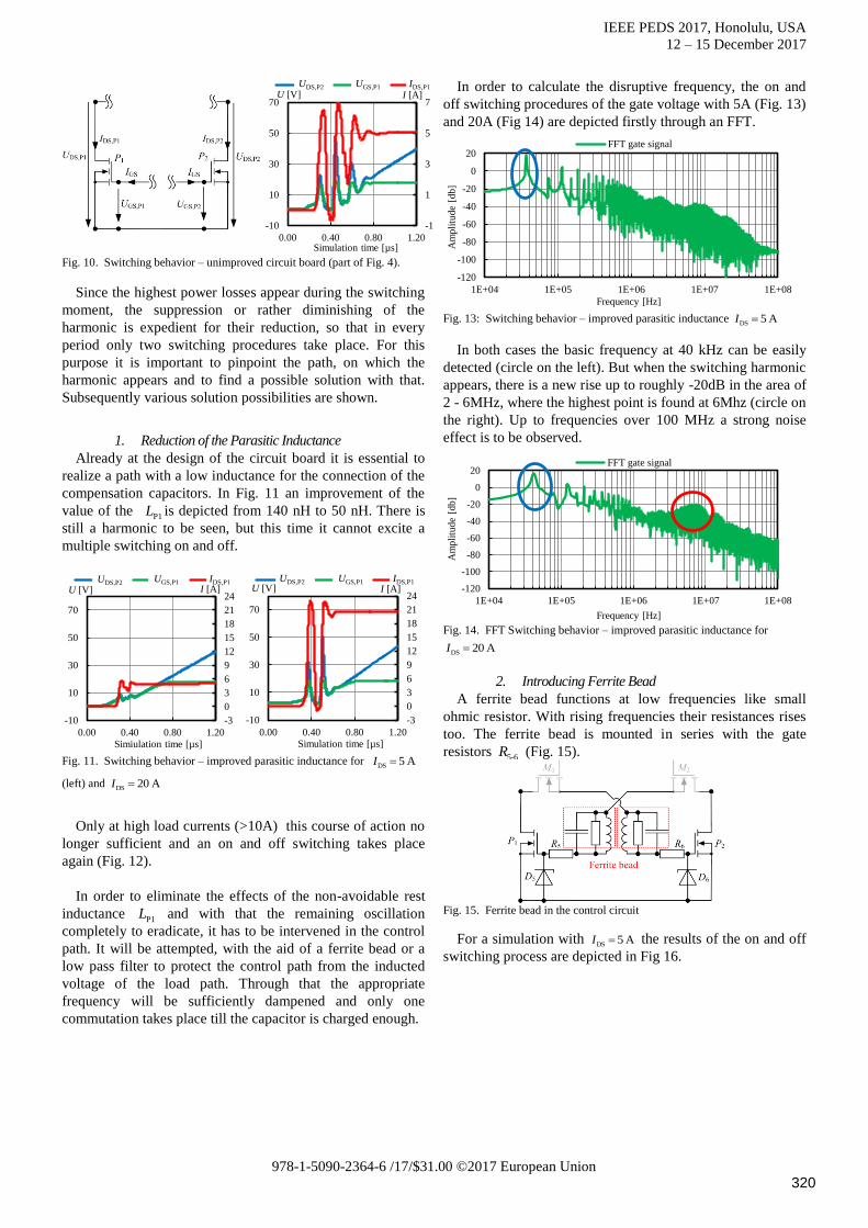
In Fig. 10 a switching operation is to be seen, at which 3
oscillations elapse till a safe switch on is ensured.
-5
5
15
25
35
45
0 5 10 15 20Simulation time [µs]
Isup IR1I [A] ISup IR1
Fig. 9. Currents of the FET supply
Fig. 8: FET supply voltage (part of Fig. 4)
0
50
100
150
200
2.88 2.89 2.90 2.91 2.92 2.93 2.94
Simulation time [ms]
L5 L11 L12 C1 Total losses
P [W]
PL5 PL11 PL12 PC1 Ptotal
Fig. 7. Power losses after the optimization of the real oscillating
circuit
319
IEEE PEDS 2017, Honolulu, USA
12 – 15 December 2017
978-1-5090-2364-6 /17/$31.00 ©2017 European Union
Since the highest power losses appear during the switching
moment, the suppression or rather diminishing of the
harmonic is expedient for their reduction, so that in every
period only two switching procedures take place. For this
purpose it is important to pinpoint the path, on which the
harmonic appears and to find a possible solution with that.
Subsequently various solution possibilities are shown.
1. Reduction of the Parasitic Inductance
Already at the design of the circuit board it is essential to
realize a path with a low inductance for the connection of the
compensation capacitors. In Fig. 11 an improvement of the
value of the P1L is depicted from 140 nH to 50 nH. There is
still a harmonic to be seen, but this time it cannot excite a
multiple switching on and off.
Only at high load currents (>10A) this course of action no
longer sufficient and an on and off switching takes place
again (Fig. 12).
In order to eliminate the effects of the non-avoidable rest
inductance P1L and with that the remaining oscillation
completely to eradicate, it has to be intervened in the control
path. It will be attempted, with the aid of a ferrite bead or a
low pass filter to protect the control path from the inducted
voltage of the load path. Through that the appropriate
frequency will be sufficiently dampened and only one
commutation takes place till the capacitor is charged enough.
In order to calculate the disruptive frequency, the on and
off switching procedures of the gate voltage with 5A (Fig. 13)
and 20A (Fig 14) are depicted firstly through an FFT.
In both cases the basic frequency at 40 kHz can be easily
detected (circle on the left). But when the switching harmonic
appears, there is a new rise up to roughly -20dB in the area of
2 - 6MHz, where the highest point is found at 6Mhz (circle on
the right). Up to frequencies over 100 MHz a strong noise
effect is to be observed.
2. Introducing Ferrite Bead
A ferrite bead functions at low frequencies like small
ohmic resistor. With rising frequencies their resistances rises
too. The ferrite bead is mounted in series with the gate
resistors 5-6R (Fig. 15).
For a simulation with
DS 5 AI the results of the on and off
switching process are depicted in Fig 16.
-3
0
3
6
9
12
15
18
21
24
-10
10
30
50
70
0.00 0.40 0.80 1.20
Simiulation time [µs]
DU UG IDU [V]
IDS,P1
I [A]UGS,P1UDS,P2
-3
0
3
6
9
12
15
18
21
24
-10
10
30
50
70
0.00 0.40 0.80 1.20Simulation time [µs]
DU UG IDUGS,P1 IDS,P1UDS,P2
I [A]U [V]
Fig. 11. Switching behavior – improved parasitic inductance for
DS 5 AI
(left) and DS 20 AI
-120
-100
-80
-60
-40
-20
0
20
1E+04 1E+05 1E+06 1E+07 1E+08
Am
pli
tud
e [d
b]
Frequency [Hz]
FFT gate signal
Fig. 14. FFT Switching behavior – improved parasitic inductance for
DS 20 AI
Fig. 15. Ferrite bead in the control circuit
-120
-100
-80
-60
-40
-20
0
20
1E+04 1E+05 1E+06 1E+07 1E+08
Am
pli
tud
e [d
b]
Frequency [Hz]
FFT gate signal
Fig. 13: Switching behavior – improved parasitic inductance
DS 5 AI
-1
1
3
5
7
-10
10
30
50
70
0.00 0.40 0.80 1.20Simulation time [µs]
DU UG IGU [V]
UDS,P2 UGS,P1 IDS,P1
I [A]
Fig. 10. Switching behavior – unimproved circuit board (part of Fig. 4).
320
IEEE PEDS 2017, Honolulu, USA
12 – 15 December 2017
978-1-5090-2364-6 /17/$31.00 ©2017 European Union
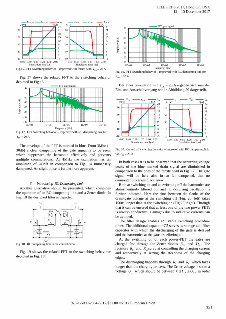
Fig. 17 shows the related FFT to the switching behavior
depicted in Fig 15.
The envelope of the FFT is marked in blue. From 3Mhz ( -
30db) a clear dampening of the gate signal is to be seen,
which suppresses the harmonic effectively and prevents
multiple commutations. At 4MHz the oscillation has an
amplitude of -40dB in comparison to Fig. 14 immensely
dampened. An slight noise is furthermore apparent.
3. Introducing RC Dampening Link
Another alternative should be presented, which combines
the operation of an RC dampening link and a Zener diode. In
Fig. 18 the designed filter is depicted.
Fig. 19 shows the related FFT to the switching behaviour
depicted in Fig. 18.
Bei einer Simulation mit DS 20 AI ergeben sich nun der
Ein- und Ausschaltvorgang wie in Abbildung 20 dargestellt.
In both cases it is to be observed that the occurring voltage
peaks of the blue marked drain signal are diminished in
comparison to the ones of the ferrite bead in Fig. 17. The gate
signal will be here also in so far dampened, that no
commutations takes place anew.
Both at switching on and at switching off the harmonics are
almost entirely filtered out and no occurring oscillation is
further indicated. Here the time between the flanks of the
drain-gate voltage at the switching off (Fig. 20, left) takes
150ns longer than at the switching on (Fig 20, right). Through
that it can be ensured that at least one of the two power FETs
is always conductive. Damages due to inductive currents can
be avoided.
The filter design enables adjustable switching procedure
times. The additional capacitor C5 serves as storage and filter
capacitor with which the discharging of the gate is delayed
and the harmonics at the gate are eliminated.
At the switching on of each power-FET the gates are
charged fast through the Zener diodes 51D and
61D . The
resistors 51R and
61R serve at controlling the charging current
and respectively at setting the steepness of the charging
edges.
The discharging happens through 5R and
6R which takes
longer than the charging process. The Zener voltage is set to a
voltage ZU which should be between Z GS0 U U in order
Fig. 18. RC dampening link in the control circuit
-3
0
3
6
9
12
15
18
21
24
-10
10
30
50
70
0.00 0.40 0.80 1.20 1.60 2.00Simulation time [µs]
U_DS U_GS I_GSI [A]U [V]
UDS UGSIGS
-3
0
3
6
9
12
15
18
21
24
-10
10
30
50
70
0.00 0.40 0.80 1.20 1.60 2.00Simulation time [µs]
U_DS U_GS I_GSU [V] I [A]
IGSUGSUDS
Fig. 20. On and off switching behavior – improved with RC dampening link
for DS 20 AI
-120
-100
-80
-60
-40
-20
0
20
1E+04 1E+05 1E+06 1E+07 1E+08
Am
pli
tude
[dB
]
Frequency [Hz]
FFT gate signal
Fig. 19. FFT Switching behavior – improved with RC dampening link for
DS 20 AI
-120
-100
-80
-60
-40
-20
0
20
1E+04 1E+05 1E+06 1E+07 1E+08
Am
pli
tud
e [d
B]
Frequency [Hz]
FFT gate signal
Fig. 17. FFT Switching behavior – improved with RC dampening link for
DS 20 AI
-3
0
3
6
9
12
15
18
21
24
-10
10
30
50
70
0.00 0.40 0.80 1.20 1.60 2.00Simulation time [µs]
1 2 3U [V] I [A]
UDS,P2 UGS,P1 IDS,P1
-3
0
3
6
9
12
15
18
21
24
-10
10
30
50
70
0.00 0.40 0.80 1.20 1.60 2.00Simulation time [µs]
1 2 3U [V] I [A]
UDS,P2 UGS,P1 IDS,P1
Fig.16. FFT Switching behavior – improved with ferrite bead
DS 20 AI
321
IEEE PEDS 2017, Honolulu, USA
12 – 15 December 2017
978-1-5090-2364-6 /17/$31.00 ©2017 European Union
to prevent that the gate voltage is discharged too slowly and
instead follows sufficiently the drain voltage. If the difference
between drain and gate voltage rises above ZU , the Zener
diode is on and can additionally discharge the gate via 51R
und 61R .
When considering the FFT of the gate-signals in Fig. 19,
there is a clear dampening of the harmonics in comparison to
the Fig. 17, where the amplitude at 3 MHz is only around -
40dB. Furthermore, the noise is considerably and continously
diminished until it disappears at 10 MHz.
Two methods will be presented which can be used in order
to reduce the described switching oscillations and to provide
a non-oscillating gate signal in overall. At the first
variant(ferrite bead) there is still noise present but its
advantage is its simple structure with only one more
component The second variant (RC dampening circuit), on
the contrary, has minimal noise and adjustable charge and
discharge times but needs therefore 4 additional components.
In the following the RC filter is going to be implemented.
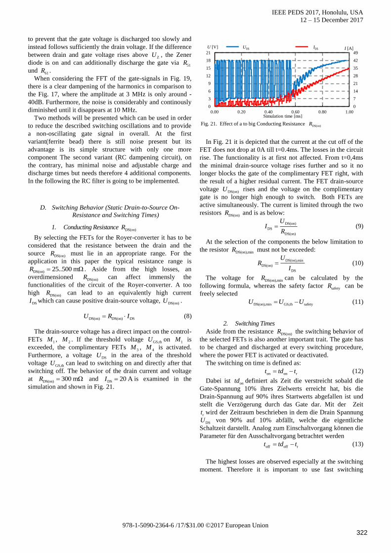
D. Switching Behavior (Static Drain-to-Source On-
Resistance and Switching Times)
1. Conducting Resistance DS(on)R
By selecting the FETs for the Royer-converter it has to be
considered that the resistance between the drain and the
source DS(on)R must lie in an appropriate range. For the
application in this paper the typical resistance range is
DS(on) 25..500 mΩR . Aside from the high losses, an
overdimensioned DS(on)R can affect immensly the
functionalities of the circuit of the Royer-converter. A too
high DS(on)R can lead to an equivalently high current
DSI which can cause positive drain-source voltage, DS(on)U .
DS(on) DS(on) DSU R I (8)
The drain-source voltage has a direct impact on the control-
FETs 1M ,
2M . If the threshold voltage GS,thU on
1M is
exceeded, the complimentary FETs 3M ,
4M is activated.
Furthermore, a voltage DSU in the area of the threshold
voltage GS,thU can lead to switching on and directly after that
switching off. The behavior of the drain current and voltage
at DS(on) 300 mΩR and DS 20 AI is examined in the
simulation and shown in Fig. 21.
In Fig. 21 it is depicted that the current at the cut off of the
FET does not drop at 0A till t=0.4ms. The losses in the circuit
rise. The functionality is at first not affected. From t=0,4ms
the minimal drain-source voltage rises further and so it no
longer blocks the gate of the complimentary FET right, with
the result of a higher residual current. The FET drain-source
voltage DS(on)U rises and the voltage on the complimentary
gate is no longer high enough to switch. Both FETs are
active simultaneously. The current is limited through the two
resistors DS(on)R and is as below:
DS(on)
DS
DS(on)
UI
R (9)
At the selection of the components the below limitation to
the resistor DS(on),minR must not be exceeded:
DS(on),min
DS(on)
DS
UR
I (10)
The voltage for DS(on),minR can be calculated by the
following formula, whereas the safety factor safetyR can be
freely selected
DS(on),min GS,th safetyU U U (11)
2. Switching Times
Aside from the resistance DS(on)R the switching behavior of
the selected FETs is also another important trait. The gate has
to be charged and discharged at every switching procedure,
where the power FET is activated or deactivated.
The switching on time is defined as:
on on rt td t (12)
Dabei ist ontd definiert als Zeit die verstreicht sobald die
Gate-Spannung 10% ihres Zielwerts erreicht hat, bis die
Drain-Spannung auf 90% ihres Startwerts abgefallen ist und
stellt die Verzögerung durch das Gate dar. Mit der Zeit
rt wird der Zeitraum beschrieben in dem die Drain Spannung
DSU von 90% auf 10% abfällt, welche die eigentliche
Schaltzeit darstellt. Analog zum Einschaltvorgang können die
Parameter für den Ausschaltvorgang betrachtet werden
off off rt td t (13)
The highest losses are observed especially at the switching
moment. Therefore it is important to use fast switching
0
7
14
21
28
35
42
49
0
3
6
9
12
15
18
21
0.00 0.20 0.40 0.60 0.80 1.00Simulation time [ms]
drain voltage P1 drain current P1U [V] I [A]UDS IDS
Fig. 21. Effect of a to big Conducting Resistance
DS(on)R
322
IEEE PEDS 2017, Honolulu, USA
12 – 15 December 2017
978-1-5090-2364-6 /17/$31.00 ©2017 European Union
power-FETs to reduce the losses. Typical switching times
range in the area of on off 70..150 nst t .
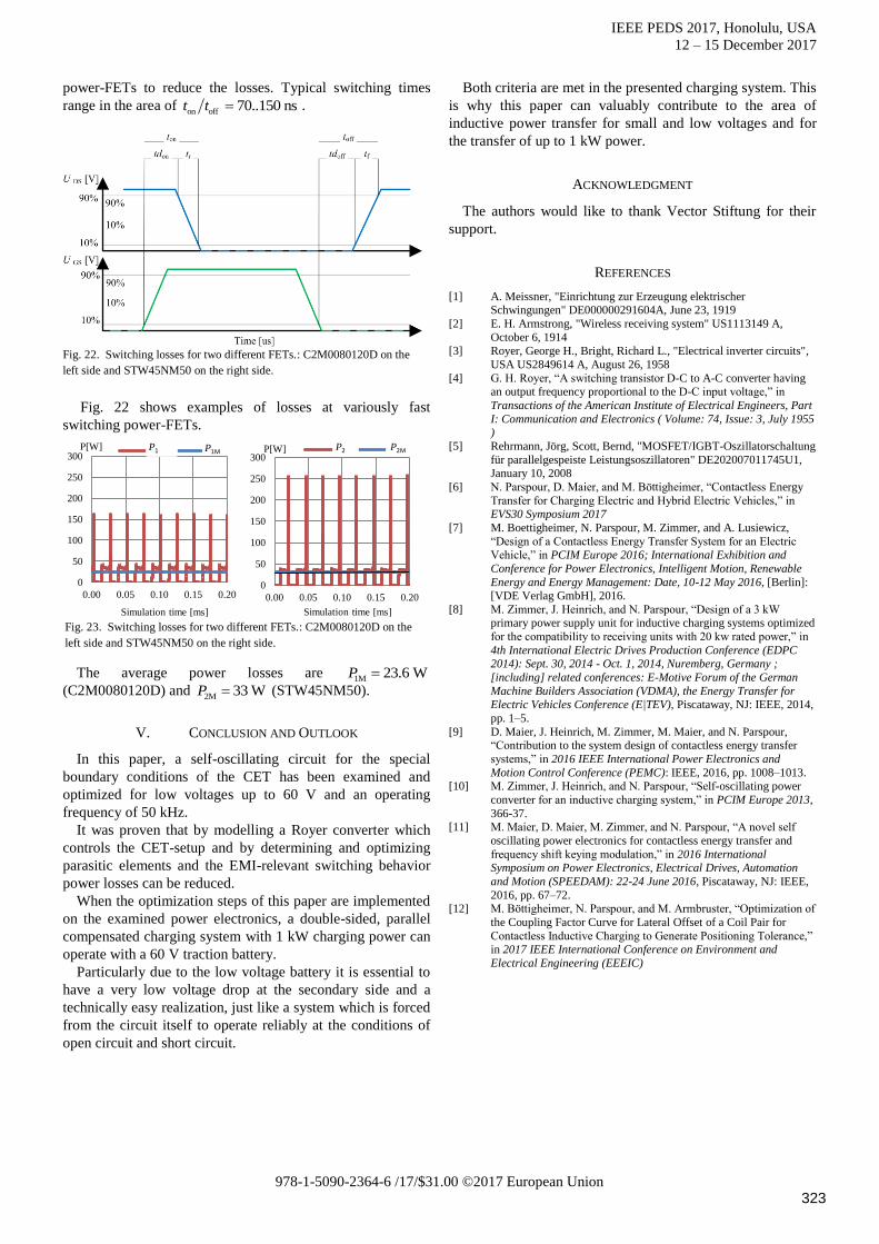
Fig. 22 shows examples of losses at variously fast
switching power-FETs.
The average power losses are 1M 23.6 WP
(C2M0080120D) and 2M 33 WP (STW45NM50).
V. CONCLUSION AND OUTLOOK
In this paper, a self-oscillating circuit for the special
boundary conditions of the CET has been examined and
optimized for low voltages up to 60 V and an operating
frequency of 50 kHz.
It was proven that by modelling a Royer converter which
controls the CET-setup and by determining and optimizing
parasitic elements and the EMI-relevant switching behavior
power losses can be reduced.
When the optimization steps of this paper are implemented
on the examined power electronics, a double-sided, parallel
compensated charging system with 1 kW charging power can
operate with a 60 V traction battery.
Particularly due to the low voltage battery it is essential to
have a very low voltage drop at the secondary side and a
technically easy realization, just like a system which is forced
from the circuit itself to operate reliably at the conditions of
open circuit and short circuit.
Both criteria are met in the presented charging system. This
is why this paper can valuably contribute to the area of
inductive power transfer for small and low voltages and for
the transfer of up to 1 kW power.
ACKNOWLEDGMENT
The authors would like to thank Vector Stiftung for their
support.
REFERENCES
[1] A. Meissner, "Einrichtung zur Erzeugung elektrischer Schwingungen" DE000000291604A, June 23, 1919
[2] E. H. Armstrong, "Wireless receiving system" US1113149 A,
October 6, 1914
[3] Royer, George H., Bright, Richard L., "Electrical inverter circuits",
USA US2849614 A, August 26, 1958
[4] G. H. Royer, “A switching transistor D-C to A-C converter having an output frequency proportional to the D-C input voltage,” in
Transactions of the American Institute of Electrical Engineers, Part
I: Communication and Electronics ( Volume: 74, Issue: 3, July 1955 )
[5] Rehrmann, Jörg, Scott, Bernd, "MOSFET/IGBT-Oszillatorschaltung
für parallelgespeiste Leistungsoszillatoren" DE202007011745U1, January 10, 2008
[6] N. Parspour, D. Maier, and M. Böttigheimer, “Contactless Energy
Transfer for Charging Electric and Hybrid Electric Vehicles,” in EVS30 Symposium 2017
[7] M. Boettigheimer, N. Parspour, M. Zimmer, and A. Lusiewicz,
“Design of a Contactless Energy Transfer System for an Electric Vehicle,” in PCIM Europe 2016; International Exhibition and
Conference for Power Electronics, Intelligent Motion, Renewable
Energy and Energy Management: Date, 10-12 May 2016, [Berlin]: [VDE Verlag GmbH], 2016.
[8] M. Zimmer, J. Heinrich, and N. Parspour, “Design of a 3 kW primary power supply unit for inductive charging systems optimized
for the compatibility to receiving units with 20 kw rated power,” in
4th International Electric Drives Production Conference (EDPC 2014): Sept. 30, 2014 - Oct. 1, 2014, Nuremberg, Germany ;
[including] related conferences: E-Motive Forum of the German
Machine Builders Association (VDMA), the Energy Transfer for Electric Vehicles Conference (E|TEV), Piscataway, NJ: IEEE, 2014,
pp. 1–5.
[9] D. Maier, J. Heinrich, M. Zimmer, M. Maier, and N. Parspour, “Contribution to the system design of contactless energy transfer
systems,” in 2016 IEEE International Power Electronics and
Motion Control Conference (PEMC): IEEE, 2016, pp. 1008–1013. [10] M. Zimmer, J. Heinrich, and N. Parspour, “Self-oscillating power
converter for an inductive charging system,” in PCIM Europe 2013,
366-37. [11] M. Maier, D. Maier, M. Zimmer, and N. Parspour, “A novel self
oscillating power electronics for contactless energy transfer and
frequency shift keying modulation,” in 2016 International Symposium on Power Electronics, Electrical Drives, Automation
and Motion (SPEEDAM): 22-24 June 2016, Piscataway, NJ: IEEE,
2016, pp. 67–72. [12] M. Böttigheimer, N. Parspour, and M. Armbruster, “Optimization of
the Coupling Factor Curve for Lateral Offset of a Coil Pair for
Contactless Inductive Charging to Generate Positioning Tolerance,” in 2017 IEEE International Conference on Environment and
Electrical Engineering (EEEIC)
Fig. 22. Switching losses for two different FETs.: C2M0080120D on the
left side and STW45NM50 on the right side.
0
50
100
150
200
250
300
0.00 0.05 0.10 0.15 0.20
Simulation time [ms]
P1 P1MP[W] P1 P1M
0
50
100
150
200
250
300
0.00 0.05 0.10 0.15 0.20
Simulation time [ms]
P1 P1MP[W] P2 P2M
Fig. 23. Switching losses for two different FETs.: C2M0080120D on the
left side and STW45NM50 on the right side.
323