optocoupler applications for... · 5 graph 2 shows the relationship between response speed (ton,...
TRANSCRIPT

California Eastern Laboratories
OptocouplerApplications

1
DESIGNING FOR OPTOCOUPLERS WITH BASE PIN
GENERAL
Optocouplers (optical couplers) are designed to isolate electrical output from input for complete elimination of noise. They havebeen used conventionally as substitutes for relays and pulse transformers. Today's current technology in the area of microcom-puters creates new applications for optocouplers.
This manual describes the characteristics of typical optocouplers. Also included are notes on designing application circuits fortypical optocouplers (with a base pin) for better comprehension. NEC's typical optocouplers with or without base pins are listedon the following pages.

2
Absolute Maximum Ratings Electric Characteristics (TA = 25°C) (TA = 25°C)
Product name Features BV IF (mA) IC(mA) CTR (%) tr (µs) tr (µs)
(Vr.m.s.) (TYP) (TYP)
PS2601 High isolation PS2601L voltage
High VCEO 5 k 80 50 80 to 600 3 5 PS2602 (80 V MIN.) PS2602L Single transistor
PS2603 High isolation PS2603L voltage
High CTR 5 k 80 200 200 to 2500 100 100 PS2604 Darlington- PS2604L transistor
PS2605 High isolation PS2605L voltage
A.C. input 5 k ±80 50 80 to 600 3 5High VCEO
PS2606 (80 V MIN.) PS2606L Single transistor
PS2607 High isolation PS2607L voltage
A.C. input 5 k ±80 200 200 to 3400 100 100High CTR
PS2608 Darlington- PS2608L transistor
PS2621 High isolation PS2621L voltage
Large input 5 k 150 50 20 to 50 3 5 PS2622 current PS2622L Single transistor
PS2625 High isolation PS2625L voltage
A.C. input 5 k ±150 50 20 to 50 3 5Large input
PS2626 current PS2626L Single transistor
PS2633 High isolation PS2633L voltage
High VCEO 1000 to(300 V MIN.) 5 k 80 150 15000 100 100High CTR
PS2634 Darlington- PS2634L transitor
PS2651 High isolation PS2651L2 voltage
High VCEO 5 k 80 50 50 to 400 3 5(80 V MIN.)
PS2652 Single transistor PS2652L2
PS2653 High isolation PS2653L2 voltage
High CTR 5 k 80 200 200 to 3400 100 100Darlington-
PS2654 transistors PS2654L2
PS2600 Series Optocouplers (6-Pin Dual-in-Line Package)
Internalconnection
*
*
*
*
*
*
*
*
*
* (with a base pin)
Note: A product name followed by letter L indicates a product having leads formed for surface mount.

3
There are two kinds of optocouplers (a light emitting diode (LED) as an input and a phototransistor as an output) according to thetype of output transistor: Single transistor type and Darlington-transistor type.
The single-transistor type optocouplers are used to perform high-speed switching (with high-speed response). The Darlington-transistor type optocouplers are used to obtain a large output current by utilizing a small input current (independently of switchingspeeds).
Designing the circuits properly will improve the PS2601 optocoupler (Single Transistor type) by having a base pin in terms ofswitching speed, elimination of noise in input signals, and output leakage current (collector dark current, and application to high-voltage circuits).
APPLICATIONS OF OPTOCOUPLER BASE PINS
INCREASING SWITCHING SPEED
The switching speed of an optocoupler with a base pin can be increased by inserting a resistor between the base and the emitterof its phototransistor even when the optocoupler is applied to a large load resistance.Generally, the phototransistor of an optocoupler such as the PS2601 has a large photo-sensitive area on it. Accordingly, thejunction capacitance (CC-B) between the collector and the base of the phototransistor is great (up to 20 pF) and as a result itsresponse speed (turn-off time toff) is low. The relationship between turn-off time toff and collector-base capacitance CC-B isexpressed by:
toff × CC-B x hFE x RL ................(1)
wheretoff : Turn-off time (See Fig. 2-2.)CC-B : Collector-base capacitancehFE : D.C. current amplification factorRL : Load resistance
Cc-B
RL
Figure 2-1. Collector-Base Capacitance CC-B of Phototransistor

4
As judged from expression (1), the turn-off time toff is affected by collector-base capacitance CC-B, D.C. current amplificationfactor hFE, and load resistance LR. In actual circuit design, CC-B and hFE are fixed. Accordingly, the turn-off time is significantlyaffected by the resistance of load RL.
Graph 1 shows the relationship between response speed (ton,toff) and load resistance (RL) in typical emitter follower (test circuit 1)having a load resistance of 100 Ω.
PW = 100 µsDuty = 1/10
Input monitor
( )VCC = 5 V
Vo
RL = 100 Ω51 Ω
IF = 5 mA
PS2601
Inputmonitor
Vo
Graph 1Up : Input 0.2 V/DIVDOWN : Output 0.5 V/DIV
(50 µs/DIV)
Test Circuit 1
90% 90%
10% 10%
50%
Input
Output
ton toff
Figure 2-2. ton/toff Measuring Points

5
Graph 2 shows the relationship between response speed (ton, toff) and load resistance (RL) in a typical emitter follower (Testcircuit 2) having a greater load resistance (5 kΩ).
Input monitor
VCC = 5 V
Vo
RL = 5 Ω51 Ω
IF = 5 mA
PS2601
Test Circuit 2
Graph 2Up : Input 0.2 V/DIVDOWN : Output 2 V/DIV
(50 µs/DIV)
As shown in Graph 2, the turn-off time for load resistance of 5 kΩ is about 100 µs. Similarly, the turn-off time for load resistanceof 100 kΩ is 1 to 2 ms. This is also true when the load resistance is connected to the collector of the phototransistor.Graph 3 shows the relationship between response speed (ton, toff) and load resistance (RL) in a typical circuit (Test circuit 3)having collector load resistance (5 kΩ) with the emitter grounded.
Input monitor
VCC = 5 V
Vo
RL = 5 Ω
51 Ω
IF = 5 mA
PS2601
Test Circuit 3
Inputmonitor
Vo
Graph 3Up : Input 0.2 V/DIVDOWN : Output 2 V/DIV
(50 µs/DIV)
Inputmonitor
Vo
6
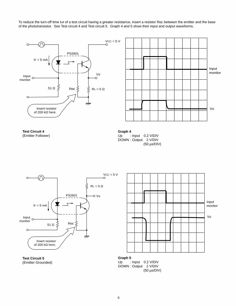
Input monitor
VCC = 5 V
Vo
RL = 5 Ω51 Ω
IF = 5 mA
PS2601
RBE
Insert resistorof 200 kΩ here.
Test Circuit 4(Emitter Follower)
Inputmonitor
Vo
Input monitor
VCC = 5 V
Vo
RL = 5 Ω
51 Ω
IF = 5 mA
PS2601
RBE
Insert resistorof 200 kΩ here.
Inputmonitor
Vo
To reduce the turn-off time toff of a test circuit having a greater resistance, insert a resistor RBE between the emitter and the baseof the phototransistor. See Test circuit 4 and Test circuit 5. Graph 4 and 5 show their input and output waveforms.
Test Circuit 5(Emitter Grounded)
Graph 5Up : Input 0.2 V/DIVDOWN : Output 2 V/DIV
(50 µs/DIV)
Graph 4Up : Input 0.2 V/DIVDOWN : Output 2 V/DIV
(50 µs/DIV)

7
The turn-off time can be greatly reduced by the base-emitter resistance (RL). In Test circuit 4, the turn-off time of the test circuithaving resistance RL is about 1/30 of that of the test circuit without the resistance. This is because the carrier (photocurrent)stored in the collector-base capacitor (CC-B) is quickly released through the base-emitter resistor (RBE). However, note that partof a photocurrent generating on the base of the phototransistor flows through the RBE resistor and reduces the current transferratio (CTR). Compare the voltage level of the output waveform in Photo 4 with that of the output waveform in Photo 2. Thecurrent transfer ratio of the test circuit having a base-emitter resistor of 200 kΩ is half or less of that of the test circuit without theresistance. (See 3.3 for reduction of the current transfer ratio CTR.)For reference, Fig. 2-3 shows the switching-time vs. RL characteristics and Fig. 2-4 shows the switching-time vs. RBE characteris-tics.
x
Sample Solid line:Current transfer ratio of 166%
Dotted line: Current transfer ratio of 274%at Ir = 5mA
t r
t d
1000
500
200
100
50
20
10
5
2
1
100 500 1 k 5 k 10 k 50 k 100 k
t f
t sIF = 10 mA Vcc = 5 V
Vcc = 5V
Vo
R L
IF =
10 mA
51Ω
I
Load Resistance RL (Ω)
VCC = 5 V, IF = 10mARL = 5ΩSolid line: Emitter followerDotted line: Emitter grounded
160
140
120
100
80
60
40
20
0100 200 500 1000 8
toff
toff
Base-Emitter Resistance RBE (kΩ)
Sw
itchi
ng T
ime
(µs)
Sw
itchi
ng T
ime
(µs)
Load Resistance RL (Ω)
1000
500
200
100
50
20
10
5
2
1100 500 1 k 5 k 10 k 50 k 100 k
t f
t s
t r
t d
VCC = 5V
Vo
R L
IF =
5 mA I
51Ω
IF = 5 mA VCC = 5 V
x
Sample Solid line:Current transfer ratio of 166%Dotted line:Current transfer ratio of 274%at Ir = 5 mA
Sw
itchi
ng T
ime
(µs)
Sw
itchi
ng T
ime
(µs)
Base-Emitter Resistance RBE (kΩ)
Vcc = 5 V, IF = 5mAR1 = 5ΩSolid line: Emitter followerDotted line: Emitter grounded
160
140
120
100
80
60
40
20
0
toff
ton
100 200 500 1000 8
Fig. 2-3 Switching-Time vs. RL Characteristics
Fig. 2-4 Switching-Time vs. RBE Characteristics

8
STABILIZING OUTPUT LEVELS
When an optocoupler is used with the base pin of its phototransistor open, the collector dark current (ICEO) flows as a basecurrent. The current is amplified as a collector current and could make the output level of the phototransistor unstable. Toeliminate this unwanted base current and make the output level stable, flow the collector dark current (ICEO) through the base-emitter resistor (RBE).Fig 2-5 shows the ICEO vs. TA characteristics of a PS2601 optocoupler.
RBE = 8
IF = 0VCE = 80V (40V for the PS2603) 2601Solid line: PS2601Dotted line: PS2603
10000
RBE = 1MΩ
RBE =100 MΩ
1000
100
10
1
0.1- 20 0 20 40 60 80 100
RBE =1MΩ
Col
lect
or D
ark
Cur
rent
I CE
O (
nA)
Ambient Temperature TA (°C)
ELIMINATION OF INDUCED NOISE
Generally, machine-controlling equipment generates induced noise which may cause malfunctions. This unwanted noise in inputsignals can be isolated by means of optocouplers. However, if the noise is too strong, it may be switched to the output throughthe input-output capacitance C1-2 of the optocoupler. This unwanted noise in the output can be removed in the following manner.Insert a capacitor (preferably 100 pF) between the base and the emitter of the phototransistor of the optocoupler. This capacitordelays response and suppresses malfunctions.
Graph 6-(a) to 6-(d) show how an external noise (surge voltage of 1000 V/µs at rise time) is eliminated as the capacitance of thebase-emitter capacitor.A fluctuation in the collector-emitter voltage caused by the on/off operation of a power switch at the output of the optocouplercauses a base current to flow through the collector-base capacitor (CCB), which causes a malfunction.In Fig. 2-7, for example, an instantaneous base current flows through the collector-base capacitor (CCB) of the optocoupler. Thecurrent is multiplied by hFE (as a collector current) and causes an output voltage on both ends of the load resistance. It seems asif an input signal was applied to the optocoupler. Graph 7-(a) shows the waveforms. This unwanted instantaneous inductioncurrent can be eliminated by inserting a capacitor CBE between the emitter and the base of the phototransistor. Graph 7-(b)shows the waveforms. Fig. 2-8 shows the output-voltage vs. CBE characteristics.
CBE
Vo
RL
Figure 2-6.
Figure 2-7.
PS2601 ICEO-TA Characteristics
Figure 2-5. ICEO vs. TA Characteristics
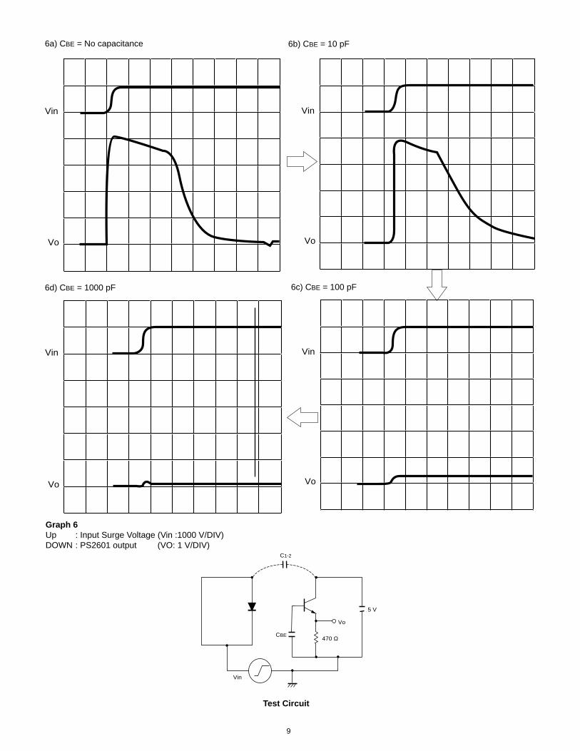
9
Vo
Vin
6a) CBE = No capacitance
Vo
Vin
6b) CBE = 10 pF
Vo
Vin
Vo
Vin
6d) CBE = 1000 pF 6c) CBE = 100 pF
Vin
Vo
5 V
470 ΩCBE
C1-2
Graph 6Up : Input Surge Voltage (Vin :1000 V/DIV)DOWN : PS2601 output (VO: 1 V/DIV)
Test Circuit

10
Vin (dV/dt = 10 V/µs, 2 V/DIV)
Vo (0.1 V/DIV)
(500 ns/DIV)
Vo
VinCCB
5 kΩ
Graph 7-(a)Input Voltage Fluctuation and Output
Vin (dV/dt = 10 V/µs, 2 V/DIV)
Vo (0.1 V/DIV)
(500 ns/DIV)
Vo
VinCCB
5 kΩ1000 pF
Graph 7-(b)Effect of Collector-Base Capacitance onVoltage Fluctuation

11
PS2601RL = 5 kΩ
1
0.1
0.01100 1000
Base-Emitter Capacitance, CBE (pF)
Out
put V
olta
ge, V
o (V
)
As mentioned above, noise induced by the fluctuation of supply voltage can be removed by proper treatment of the base pin. Forswitching of input free from induced noise at normal switching speed, optocouplers with a base pin such as the PS2602 seriesare available. If the base pin of an optocoupler is left unused or opened, it typically will pick up external noise. Cutting off thebase pin is also effective in order to prevent it from picking up external noise. See Graph 8-(b).
Figure 2-8. Vo vs. CBE Characteristics

12
Vin
Vo
(PS2601)
Base pin
Graph 8-(a)Up : Input Surge Voltage (Vin: 1000 V/DIV)DOWN : PS2601 Output (Vo: 1 V/DIV)
Cut the base pin (pin 6)
Vin
Vo
(PS2601)
Graph 8-(b)
Test Circuit
Vin
Vo
5 V
470 Ω

13
ELIMINATION OF INPUT SURGES
Unwanted external noise and output leakage currents (e.g., collector current IC) of a preceding transistor may cause the light-emitting diode (LED) of an optocoupler to light involuntarily. Usually, a circuit (connecting a resistor in parallel to the LED) isprovided to absorb such input surges. To prevent malfunction of an optocoupler, it is also effective to insert a resistor (RBE) thatincreases the input threshold current (by the use of the input-output characteristics) between the base and the emitter of thephototransistor. In this case, the current transfer ratio (CTR) must be low. (See 3.3 for Reduction of CTR.)
60
50
40
30
20
10
0
RBE = 8
200 kΩ
100 kΩ
50 kΩ
30 kΩ 20 kΩ
10 kΩ
5 kΩ
VCE = 5 V(PS2601)
1 2 3 4 5 10 20 30 40 50
Col
lect
or C
urre
nt I C
(m
A)
Figure 2-9. IC vs. IF Characteristics (Example)
Forward Current IF (mA)
APPLICATION TO HIGH POTENTIAL CIRCUIT
The withstanding voltage between the collector and the emitter of the PS2601 optocoupler is 80 V (MAX). To make theoptocoupler available to higher withstanding voltages, use the collector-base junction photodiode as a light-sensitive element andconnect a high-voltage circuit to the output of the optocoupler. In this case, the output of the photodiode must be amplifiedbecause it is smaller than the usual output.Fig. 2-10 shows an example of an optocoupler applied to a high-voltage circuit. In this sample circuit, the photocurrent (ICBL) ofthe optocoupler is fed to the base of the high-voltage transistor and a current (IF) passes forward through the light-emitting diode(LED). Fig. 2-11 shows the ICBL vs. IF characteristics. Before working on applications outside the rated values of theoptocouplers, evaluate the practical circuits fully by contacting CEL.
Col
lect
or-B
ase
Pho
tocu
rren
t IC
BL
(µA
)
Figure 2-10. Application to aHigh Voltage Circuit
Figure 2-11. ICBL vs. IF Characteristic
PS2601
ICBL
Hig
h-vo
ltage
tran
sist
or (
Tr)
200
100
504030
20
10
543
2
11 2 3 4 5 10 20 30 40 50 80
VCB = 100V(PS2601)
IF
ICBL
CTR = 274%CTR = 166%
100VA

14
NOTES ON USE OF OPTOCOUPLER BASE PIN
This chapter explains the reduction of a current transfer ratio of an optocoupler whose base and emitter are connected by aresistor (RBE) and other optocouplers that seem to be significant in the treatment of the base pin of an optocoupler.
EQUIVALENT CIRCUIT (FOR PS2601 OPTOCOUPLER)
Fig. 3-1 shows an equivalent circuit of a single-transistor optocoupler such as the PS2601.
Cj : Junction capacity of LEDCBE : Base-emitter capacitanceRD : Resistor serially connected to LEDICBL : Collector-base photocurrent generated by the light of the LEDC1-2 : Input-output capacitanceTr : Amplifying transistor
DEFINITION OF CURRENT TRANSFER RATIO (CTR)
A current transfer ratio (CTR) of an optocoupler indicates the rate of an output current IC of its phototransistor to a forward input
current (IF) flowing through its light-emitting diode (LED). The CTR is expressed by:
ICCTR = x = 100 (%) ................(2) IF
where IC = ICBL•hFE ..............................(3)
(hFE: D.C. current amplification factor of the phototransistor)
Figure 3-1. Equivalent Circuit (for PS2601 Optocoupler)
A
K
Cj
C1-2
CCB
CBE
ICBL
Tr
C
E
B
RD

15
ICBL
ICBL-I1
RBE
I1
VBE
= ( 1 - ) ................ (5)
As hFE' is equal to hFE if IF = approx. 5 mA, IC = approx. 15 mA, and RBC > 100 kΩ, expression (5) is simplified as follows:
= 1 - ................ (6)
IC' = hFE' (ICBL-I1) = hFE' ( ICBL- )
IC' = hFE' • ICBL ( 1 - ) ................ (4)
Note IC' : Output current of an optocoupler having RBE
hFE' : Amplification factor of an optocoupler having RBE
Accordingly, the ratio of output current IC' (of the optocoupler having RBE) to output current IC (of the optocoupler with the baseopen) is expressed by:
REDUCTION OF CURRENT TRANSFER RATIO (CTR) BY INSERTION OF BASE-EMITTER RESISTOR
A resistor (RBE) connected to the base and emitter pins of an optocoupler causes the reduction of the output current (reduction ofcurrent transfer ratio). This is because a part (I1) of the base current flows through the base-emitter resistor and causes a voltageequivalent to the emitter-base voltage (VBE). The base current is reduced by this current component (I1) and, as the result, thecurrent transfer ratio (CTR) goes down. The output current IC' is expressed as follows:
VBE
RBE
ICBL • RBE
VBE
IC hFE ICBL • RBE
IC' hFE' VBE
IC ICBL • RBE
IC' VBE
Figure 3-2.
•• •

16
Expression (6) indicates that the current transfer ratio (CTR) is significantly affected by the value of ICBL • RBE. For example, ifthe forward current IF of the light-emitting diode is smaller (that is, ICBL is smaller) or if the base-emitter resistance RBE is smaller,the reduction rate (rate of IC') becomes greater.The above CTR reduction must be considered when inserting a resistor between the emitter and the base of the phototransistorof the optocoupler to increase the switching speed. The performance of the optocoupler might become unstable because theCTR will be affected by time elapse or temperature change (even if it is initially stable).Fig. 3-3 shows the ∆CTR-RBE characteristics.
Normalized to 1.0at RBE = ×
IF = 1 mA, VCE = 5V
CTR = 274%
CTR =166%
1.0
0.8
0.6
0.4
0.2
0100 200 300 400 500 1000
8
Base Emitter Resistance RBE (kΩ)
CT
R R
elat
ive
Val
ues
CT
R R
elat
ive
Val
ues
Base Emitter Resistance RBE (kΩ)
Base Emitter Resistance RBE (kΩ)
CT
R R
elat
ive
Val
ues
Figure 3-3. ∆CTR-RBE Characteristics
CTR = 274%
CTR =166%
1.0
0.8
0.6
0.4
0.2
0100 200 300 400 500 1000
8
Normalized to 1.0at RBE = ×
IF = 10 mA, VCE = 5V
CTR = 274%
CTR =166%
Normalized to 1.0at RBE = ×
IF = 5 mA, VCE = 5V
1.0
0.8
0.6
0.4
0.2
0100 200 300 400 500 1000
8

17
= ( ) ................ (8)
When resistor RBE is serially connected to resistor RL (see Fig. 3-4 (c)), the reduction of a CTR becomes greater even if hFE2 isapproximately equal to hFE0 in expression (8) as the expression includes RL as a parameter.Fig. 3-5 shows typical V0 vs. IF characteristics of the above circuits (a), (b), and (c).
Out
put v
olta
ge V
o (V
)
IF
PS2601
RBE = 100 kΩ
Vo
Vcc = 10V
RL = 470 kΩ
Forward current IF (mA)
Figure 3-5. Vo vs. IF Characteristics
The reduction of a CTR is greatly affected by the positional relationship between load resistor RL and base-emitter resistor RBE,as shown in Fig. 3-4 (b) and 3-4 (c).
= ( 1 - ) ................ (7)V1 hFE1 VBE
V2 hFE0 ICBL • RBE1
The output voltage V0, V1, and V2 of the above circuits (a), (b), and (c) are related as follows:
V2 hFE2
V0 hFE0
VBE21 -
ICBL • RBE1
RL • hFE21 +
RBE2
Figure 3-4 (a).
Open
ICBL
VBE
Vo
RL
ICBL
RBE1 VBE1
V1
RL
Figure 3-4 (b).
RBE Serial to RL
ICBL
RBE2 VBE2
V2
RL
Figure 3-4 (c).
RBE Parallel to RL
10
8
6
4
2
01 2 5 10 20 50
(c) RBG = 100 kΩ
(b) RBE = 100 kΩ
(a) RB openVcc = 10 VRL = 470 ΩCTR = 190%(PS2601)

18
VCC - VCE 5 - 0.8I2 ⊕ = = 8.2 (mA) ................(9) R2 0.51 (kΩ)
Therefore I3 = I2 + I4 = 8.2 + 1.6 = 9.8 (mA) ................(10)
Let's assume that hFE of transistor Tr1 is 40 (worst). Ib must be as follows:
I3 9.9 (mA)Ib ⊕ = = 0.247 (mA) ................(11) hFE 40
Similarly, let's assume that VBE of transistor Tr1 is 0.8 V (worst), I1 must be as follows:
VBE 0.8I1 = = = 0.4 (mA) ................(12) R1 2 (kΩ)
Therefore, the output current I0 of the optocoupler is
I0 ⊕ I1 + Ib = 0.647 (mA) ................ (13)
If forward current IF is 3 mA (worst) (normally IF = 5 mA), the CTR is calculated as follows:
I0 0.647(mA)CTR = x 100 = x 100 = 21.6% ................(14)
IF 3 (mA)
CIRCUIT DESIGN EXAMPLE (USING THE PS2601)
Fig. 4-1 shows a design example of an optocoupler circuit having a base-emitter resistor for improvement of response ability.
The minimum current transfer ratio (CTR) required for TTL operation is calculated as follows:Current I4 must be 1.6 mA to drive the TTL and the collector-emitter voltage of transistor Tr1 must be 0.8 V or less. Accordingly, I2must be as follows:
A resistor of 510 kΩis inserted here.
PS2601
IF = 5 mA
I0
I1
Vcc = 5 V
VOUT
G
I3
I4
Tn1
Ib
R2 = 510 Ω
TTL
R0 = 1 kΩ
R1
= 2 kΩ
Figure 4-1. Circuit Design Example

19
A design example of an optocoupler circuit that operates for at least ten years is shown below (using Fig. 3-3, 4-2 and 4-3). Themajor causes of CTR reduction area as follows:
(From Fig. 3-3) CTR-relative-value vs. RBE characteristics15% down (with respect to initial value, RBE = ×)
(From Fig. 4-2) CTR change with time (10 years, Ta = 60 °C)40% down (with respect to initial value, 0 year)
(From Fig. 4-3) CTR-relative-value vs. ambient-temperature characteristics(Ta = 60 °C)15% down (with respect to initial value ta = 25 °C)
Considering the above characteristics and safety factor = 2 (twice margin), the recommended CTR is:
21.6 x 1.4 x 1.15 x 1.15 x 2 = 80%.................(15)
(Reference)
Accordingly, the CTR value including reduction of CTR by time elapse, temperature change, and insertion of RBE must be 21.6 %or more.
IF = 5 mATA = 25˚C
IF = 20 mATA = 25˚C
IF = 5 mATA = 60˚C
Normalized to CTRtest conditonIF = 5 mA, VCE = 5V
1.2
1.0
0.8
0.6
0.4
0.2
00 10 10 10 102 3 4 5
Time (Hr)
Figure 4-2. Change of CTR withTime (PS2601)
CT
R R
elat
ive
Val
ue
Ambient Temperature TA (°C)
Figure 4-3. CTR-Relative-Value vs.TA Characteristics
CT
R R
elat
ive
Val
ue
Normalized to 100at TA = 25˚CIF = 5 mA, VCE = 5 V
1.2
1.0
0.8
0.6
0.4
0.2
0-55 -40 -20 20 40 60 80 1000

20
GENERAL
Recently, optocouplers have been supplanting relays and pulse transformers for complete noise elimination, level conversion,and high-potential isolation. Microprocessor systems are requiring more and more optocouplers on the limited area of PC boardsfor I/O interface and other purposes. For these requirements, NEC has manufactured multi-channel optocouplers having 4 pins(for one channel) to 16 pins (for four channels). These multi-channel optocouplers are called the PS2500 series optocouplers.The PS2500 series optocouplers are divided into PS2501, PS2502, PS2505, and PS2506 according to their functions.(PS2501L, PS2502L, PS2505L, and PS2506L have leads formed for surface installation.)
This manual describes features, structures, and basic characteristics of the PS2500 series optocouplers.
FEATURES, STRUCTURES, AND PACKAGE DIMENSIONS
Features
The major feature of PS2500 is very high isolation voltage between input and output (substantially two to three times that of theconventional PS2400 series optocouplers). This can be proved because none of the 1300 test optocouplers were destroyed in astrict product test (applying 10 kVac to each optocoupler for one minute). The improvement in dielectric strength of the PS2500optocouplers has been accomplished by the double molding package structure.
In addition to high isolation voltage, the PS2500 optocouplers boast high heat resistance and high moisture resistance. Table 1lists the major features of the PS2500 series optocouplers.
Features High isolation Abundant I/O functions High CTR High VCEO ResponseProduct Voltage (TYP) (MIN) (TYP)name
PS2501 D.C. input, Single 300% 80V tr = 3 µsPS2501L (*) transistor output tr = 5 µs
PS2502 D.C. input, Darlington 2000% 40V tr, tf = 100 µsPS2502L (*) pair transistor output
PS2505 A.C. input, single 300% 80V tr = 3 µsPS2505L (*) transistor output tr = 5 µs
PS2506 A.C. input, Darlington 2000% 40V tr, tf = 100 µsPS2506L (*) pair transistor output
5 kVac
Table 1. Features of PS2500 OptocouplersNote: Tested in oil (In the air, unwanted arc discharging will occur at 6 to 7 kVac.)* The product name followed by letter L is for a product having leads for surface mount.
PS2500-SERIES MULTI-CHANNEL OPTOCOUPLERS

21
Optocoupler Structure
Figure 1 shows the internal perspective view of a PS2500 optocoupler and Figure 2 shows the sectional view of the optocoupler.Figure 2 below shows the optocoupler in a light-tight epoxy resin housing, and a light-sensitive element (phototransistor or photoDarlington transistor) with light-transmittable epoxy resin medium between them. A light signal emitted by the LED is transferredto the photosensitive transistor via the internal resin medium.Both the housing resin and the internal resin have the same expansion coefficient. Namely, the optocoupler elements are moldedtwice with epoxy resin. (This structure is referred to as a double molding structure.)The high isolation voltage is obtained by the long adjacent area of the inner and outer resins (inner boundary) and identicalexpansion coefficient of the inner and outer resins (eliminating arc discharges on the inner boundary).
Figure 1. Internal perspective view of optocoupler
Outer resin (Black)
Inner resin (White)
Inner boundary
Figure 2. Sectional view of optocoupler

22
Dimensions
Figures 3 and 4 show the dimensions of the PS2500 series optocouplers. The PS2500 series optocouplers are very compactand fit for high-density installation on PC boards. For example, the package area occupied by a single channel of the PS2500series is half that of the PS2600 series (6-pin Dual in-line package).
PS250X-1
PS250X-4
Figure 3. Package Dimensions (Units in mm) (PS2501, PS2502, PS2505, and PS2506)
16151413
1 2 3 41,3,5,7. Anode2,4,6,8. Cathode9,11,13,15. Emitter10,12,14,16. Collector
20.3 MAX
6.5
3.8
MA
X
4.55
MA
X2.
8M
IN
1.34
0.65
0.50±0.10
2.54 7.62
0 to 15˚0.25 M
5 6
1211
7 8
10 9
PS250X-28 7 6 5
1 2 3 4
1,3. Anode2,4. Cathode5,7. Emitter6,8. Collector
10.2 MAX
6.5
3.8
MA
X
4.55
MA
X
2.8
MIN
1.34
0.65
0.50±0.10
2.54 7.62
0.25 M 0 to 15˚
4 3
1 2
5.1 MAX
1.34
6.5
0.50±0.100 to 15˚
7.622.54
3.8
MA
X
4.55
MA
X2.
8M
IN
0.65
0.25 M
1. Anode2. Cathode3. Emitter4. Collector

23
4 3
1 2
5.1 MAX
1.34±0.10
9.60±0.4
7.62
2.54
3.8
MA
X.
0.25 M
6.5
0.9±0.25
0.05
to 0
.2
1. Anode2. Cathode3. Emitter4. Collector
Fig. 4 Package Dimensions (Units in mm) (PS2501L, PS2502L, PS2505L, and PS2506L)
Lead Bending type (Gull-wing)
PS250XL-1 PS250XL-2
12 11
5 620.3 MAX
1.34±0.10
9.60±0.4
7.62
2.54
3.8
MA
X.
0.25 M
6.5
0.9±0.25
0.05
to 0
.2
3 4
14 13
7 8
10 9
1 2
16 15
1,3,5,7. Anode2,4,6,8. Cathode9,11,13,15. Emitter10,12,14,16. Collector
PS250XL-4
6 5
3 4
10.2 MAX
1.34±0.10
9.60±0.4
7.62
2.54
3.8
MA
X.
0.25 M
6.5
0.9±0.25
0.05
to 0
.2
1 2
8 7
1,3. Anode2,4. Cathode5,7. Emitter6,8. Collector

24
CT
R R
elat
ive
Val
ue
CT
R R
elat
ive
Val
ue
Time (Hr) Time (Hr)Figure 6.Figure 5.
CTR vs. TA Characteristics (TA: Ambient Temperature)
The CTR-Temperature characteristic is greatly affected by the total characteristics of light-emission efficiency of the LED and hFE
of the phototransistor as the light-emission efficiency has a negative temperature coefficient and hFE has a positive temperaturecoefficient. See Figure 7.
Ligh
t-em
issi
onef
ficie
ncy
of L
ED
hFE o
f pho
totr
ansi
stor
CT
R
TA TA TA
Figure 7. CTR vs. TA Characteristics
Current Transfer Ratio (CTR)
The current transfer ratio (CTR) of an optocoupler is the ratio of the value of output current IC to the value of input forward currentIF (IC/IF x 100%). The CTR is a parameter equivalent to the D.C. current amplification factor hFE of a transistor.The CTR is one of the most significant characteristics of optocouplers, as well as isolation voltage. In circuit designing, CTR mustbe considered first of all because the CTR:
1 varies as time goes by,2 is affected by ambient temperature, and3 is dependent upon forward current IF flowing through the LED.
Both PS2505 and PS2506 optocouplers (bidirectional input type) have two current transfer ratios (CTRs) because they have twoLEDs in the input. For further information, refer to Applications of Optocouplers for A.C. input.
Change of CTR over time
The current transfer ratio (CTR) of an optocoupler is determined by the light-emission efficiency of the LED (emitting infraredlight), efficiency of light transmission between the LED and the phototransistor, light sensitivity of the phototransistor, and hFE ofthe transistor.The change of a CTR over time is mainly caused by reduction of the light-emission efficiency of the LED. Generally, the CTR isreduced to a greater extent as the forward current IF increases or as the operating temperature increases. Figure 5 and 6respectively show estimated changes of CTRs of PS2501 and PS2505 optocouplers over time.
Estimated change of CTRs with time lapse (Standard values)
CHARACTERISTICS OF PS2501 AND PS2505 OPTOCOUPLERS
Standard valueContinuous supply of 20 mA (IF)
TA = 60˚C TA = 25˚C
1.2
1.0
0.8
0.6
0.4
0.2
0 10 10 10 10 102 3 4 5 6
1.2
1.0
0.8
0.6
0.4
0.2
0 10 10 10 102 3 4 5
Standard characteristics
IF = 5 mATA = 60˚C
IF = 20 mATA = 25˚CIF = 5 mATA = 25˚C

25
(a) (b)
Normalized to1.0 at TA = 25˚C
Standard characteristicsIF = 1 mA, VCE = 5V
1.50
1.25
1.00
0.75
0.50
0.25
0-50 -25 0 25 50 75 100
CT
R R
elat
ive
Val
ue
Standard characteristicsIF = 5 mA, VCE = 5V
Normalized to1.0 at TA = 25˚C
1.2
1.0
0.8
0.6
0.4
0.2
0
-50 -25 0 25 50 75 100
Ambient Temperature TA (°C) Ambient Temperature TA (°C)
(c)
CT
R R
elat
ive
Val
ue
Normalized to1.0 at TA = 25˚C
Standard characteristicsIF = 0.3 mA, VCE = 5V
1.6
1.50
1.25
1.00
0.75
0.50
0.25
0-50 -25 0 25 50 75 100
(d)
Normalized to1.0 at TA = 25*CIF = 5 mA,VCE = 5V
Standard characteristicsCTR = approx. 200%
1.2
1.0
0.8
0.6
0.4
0.2
0-50 -25 0 25 50 75 100
Ambient Temperature TA (°C) Ambient Temperature TA (°C)
(e) (f)
Normalized to1.0 at TA = 25˚CIF = 5 mA,VCE = 5V
Standard characteristicsCTR = approx. 300%
1.2
1.0
0.8
0.6
0.4
0.2
0-50 -25 0 25 50 75 100
CT
R R
elat
ive
Val
ue
Normalized to1.0 at TA = 25˚CIF = 5 mA, VCE = 5V
Standard characteristicsCTR = approx. 400%
1.2
1.0
0.8
0.6
0.4
0.2
0
-50 -25 0 25 50 75 100
Ambient Temperature TA (°C) Ambient Temperature TA (°C)
(g)
Normalized to1.0 at TA = 25˚CIF = 5 mA, VCE = 5V
Standard charcteristicsCTR = approx. 500%
1.2
1.0
0.8
0.6
0.4
0.2
0-50 -25 0 25 50 75 100
CT
R R
elat
ive
Val
ue
Ambient Temperature TA (°C)
CT
R R
elat
ive
Val
ueC
TR
Rel
ativ
e V
alue
CT
R R
elat
ive
Val
ue
Figure 8-(a) to Figure 8-(g) show CTR vs. TA characteristics under various conditions.

26
Standard characteristicsVCE = 5V
600
500
400
300
200
100
0 0.1 0.5 1 5 10 50
Sample A
Sample B
CT
R (
%)
Forward Current IF (mA)
Figure 9. CTR vs. IF Characteristics (Standard Value)
Response Characteristics
The response characteristics of optocouplers are the same as those phototransistors. The fall time tf is expressed by:
tf RL•hFE•CCB
RL: Load resistancehFE: Amplification factorCCB: Collector-base capacitance
If RL is too high, tf becomes too high to be fit for high-speed signal transmission. Select the proper load resistance for the desiredsignal rate. Similarly, the collector current must fully satisfy the minimum value of the CTR, CTR vs. TA characteristics, and CTRvs. time characteristics. Otherwise, the phototransistor will operate unsaturated, causing lower response characteristics andmalfunction.
Figures 10 to 13 show the response-time vs. forward current characteristics and response-time vs. VCC characteristics, using loadresistance and ambient temperature as parameters.
CTR vs. IF Characteristics (IF: Forward Current Flowing Through the LED)
The current transfer ratio (CTR) depends upon the magnitude of a forward current (IF). When IF goes lower or higher than aproper magnitude, the CTR becomes smaller. Figure 9 shows the CTR vs. IF characteristics.Note that rate changes of CTRs are very diffrent at low IF magnitude (approx. 5 mA), middle IF magnitude (approx. 5 mA), andhigh IF magnitude (approx. 20 mA). Namely, the CTR depends heavily upon the magnitude of forward current IF in lower andhigher current ranges.For low-input and high-output switching, see Chapter 4.

27
Res
pons
e Ti
me
(µs)
Forward Current IF (mA) Forward Current IF (mA)
Res
pons
e Ti
me
(µs)
VCC (V)
Res
pons
e Ti
me
(µs)
Res
pons
e Ti
me
(µs)
Figure 12. Response-Time vs. VCC
CharacteristicsFigure 13. Response-Time vs. VCC
Characteristics
For reference, a voltage-gain vs. frequency characteristic using CTR as a parameter is shown below.
Figure 10. Response-Time vs. IFCharacteristics
Figure 11. Response-Time vs. IFCharacteristics
VCC (V)
Standard characteristicsVCC = 5 V TA = 25˚CRL = 4.7 kΩ TA = 85˚C
1000
500
200
100
50
20
10
5
2
10 5 10
toff
ts
ton
td
Standard characteristicsVCC = 5 V TA = 25˚CRL = 10 kΩ TA = 85˚C
toff
ts
ton
td
1000
500
200
100
50
20
10
5
2
10 5 10
Standard characteristicsIF = 10 mA TA = 25˚CRL = 3 kΩ TA = 85˚C
toff
ts
ton
td
1000
500
200
100
50
20
10
5
2
10 5 10
Standard characteristicsIF = 10 mA TA = 25˚C
RL = 10 kΩ TA = 85˚C
toff
ts
ton
td
1000
500
200
100
50
20
10
5
2
10 5 10

28
Vol
tage
Gai
n (d
B)
Frequency f (HZ)
Test Circuit and Condition
1 kΩ 51 Ω VCC = 10 V
330 µF
1 kΩ
V O
IC = 2.25 mA
Other Temperature Characteristics
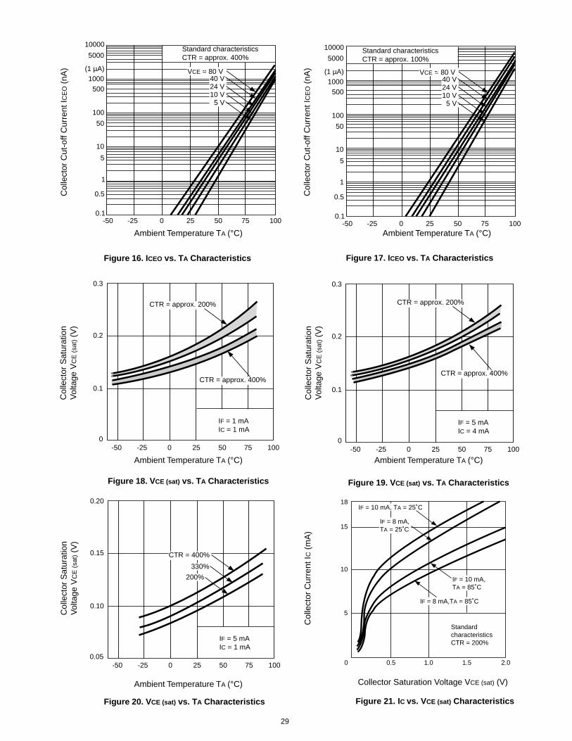
Almost all characteristics of optocouplers are apt to be affected by ambient temperature (see 3.1.2). Figures 15 to 21 show howVF (Forward Voltage), ICEO (Collector Cut-Off Current), and VCE (sat) (Collector Saturation Voltage) are affected by ambienttemperature.
Figure 14. Voltage-Gain vs. Frequency Characteristics(Standard Value) (PS2501, PS2505).
For
war
d V
olta
ge V
F (
V)
Ambient Temperature TA (°C)
Figure 15. VF vs. TA Characteristics
Standardcharacteristics
CTR = 156%
CTR = 186%
CTR = 304%
5
0
-5
-10
-15
-20
-25100 500 1 k 5 k 10 k 50 k 100 k 500 k
1.2
1.1
1.0
0.9
0.8
0.7
0.6
0.5-30 0 25 50 75 100
IF = 10 mA
IF = 1 mA
IF = 5 mA
29
Ambient Temperature TA (°C) Ambient Temperature TA (°C)
Col
lect
or C
ut-o
ff C
urre
nt I C
EO
(nA
)
Col
lect
or C
ut-o
ff C
urre
nt IC
EO
(nA
)
Col
lect
or S
atur
atio
nV
olta
ge V
CE
(sa
t) (
V)
Col
lect
or S
atur
atio
nV
olta
ge V
CE
(sa
t) (
V)
Ambient Temperature TA (°C) Ambient Temperature TA (°C)
Col
lect
or S
atur
atio
nV
olta
ge V
CE
(sa
t) (
V)
Ambient Temperature TA (°C)
Col
lect
or C
urre
nt I C
(m
A)
Figure 20. VCE (sat) vs. TA Characteristics
Figure 18. VCE (sat) vs. TA Characteristics
Figure 16. ICEO vs. TA Characteristics Figure 17. ICEO vs. TA Characteristics
Figure 19. VCE (sat) vs. TA Characteristics
Collector Saturation Voltage VCE (sat) (V)
Figure 21. IC vs. VCE (sat) Characteristics
CTR = approx. 200%
0.3
0.2
0.1
0-50 -25 0 25 50 75 100
IF = 1 mAIC = 1 mA
CTR = approx. 400%
CTR = approx. 200%
0.3
0.2
0.1
0-50 -25 0 25 50 75 100
IF = 5 mAIC = 4 mA
CTR = approx. 400%
CTR = 400%
0.20
0.15
0.10
0.05-50 -25 0 25 50 75 100
IF = 5 mAIC = 1 mA
330%
200%
18
15
10
5
0.50 1.0 1.5 2.0
StandardcharacteristicsCTR = 200%
IF = 10 mA,TA = 85˚C
IF = 8 mA,TA = 85˚C
IF = 8 mA,TA = 25˚C
IF = 10 mA, TA = 25˚C
Standard characteristicsCTR = approx. 400%
10000
5000
(1 µA)1000
500
100
50
10
5
1
0.5
0.1-50 -25 0 25 50 75 100
VCE = 80 V40 V24 V10 V
5 V
Standard characteristicsCTR = approx. 100%
10000
5000
(1 µA)1000
500
100
50
10
5
0.5
0.1-50 -25 0 25 50 75 100
1
VCE = 80 V40 V24 V10 V
5 V

30
At normal temperature (TA = 25 °C), the collector cut-off current ICEO is very little (about 1 nA (at VCE = 80 V and CTR = about400% )), but it will be multiplied by about 10 at an increment of 25°C. This needs to be kept in mind when using a small outputcurrent (IC) of an optocoupler with a high load.The rate change of VCE (sat) (Collector Saturation Voltage) is about 0.7% per °C at ambient temperature of 0°C to 70°C. In circuitdesign, the collector output current IC should be determined under the condition of half or less of the CTR rated values. Other-wise, the saturation voltage VCE (sat) will become greater.
CHARACTERISTICS OF PS2502 AND PS2506 OPTOCOUPLERS
The PS2502 and PS2506 optocouplers are higher in sensitivity than the PS2501 and PS2505 optocouplers and can be driven bylow currents.
CTR-Related Characteristics
The PS2502 and PS2506 optocouplers assure CTR ⊕ 200% at IF = 1 mA and can be directly driven by CMOS output signals.See 3.1 for CTR definition and characteristics.
Change of CTR Over time
Figure 22 shows the CTR vs. time characteristics of the PS2502 and PS2506 optocouplers.
Figure 22. CTR vs. Time Characteristics (Standard Value)
Standard values Continuous supply of IF = 1 mA
1.2
1.0
0.8
0.6
0.4
0.2
010 10 10 10 10 105432
TA = 25˚C
TA = 60˚C
Time (Hr)
CT
R R
elat
ive
Val
ue

31
CT
R R
elat
ive
Val
ue
Standard characteristics
Normalized to1.0 at TA = 25˚CIF = 0.1 mA, VCE = 2V
1.4
1.2
1.0
0.8
0.6
0.4
0.2
0-50 -25 0 25 50 75 100
Standard characteristics
Normalized to1.0 at TA = 25˚CIF = 0.3 mA, VCE = 2V
1.4
1.2
1.0
0.8
0.6
0.4
0.2
0-50 -25 0 25 50 75 100
Standard characteristics
Normalized to1.0 at TA = 25˚CIF = 1 mA, VCE = 2V
1.4
1.2
1.0
0.8
0.6
0.4
0.2
0-50 -25 0 25 50 75 100
CT
R r
elat
ive
valu
e
23-(a)
CT
R R
elat
ive
Val
ue
23-(b)
Ambient Temperature TA (°C) Ambient Temperature TA (°C)
23-(c)C
TR
rel
ativ
e va
lue
23-(d)
Ambient Temperature TA (°C) Ambient Temperature TA (°C)
CT
R R
elat
ive
Val
ue
23-(e) 23-(f)
Ambient Temperature TA (°C) Ambient Temperature TA (°C)
CT
R R
elat
ive
Val
ue
CTR vs. Temperature Characteristics
Figure 23-(a) to 23-(f) show CTR vs. Temperature Characteristics under various conditions.
Normalized to1.0 at TA = 25˚CIF = 1 mA, VCE = 2V
1.4
1.2
1.0
0.8
0.6
0.4
0.2
0-50 -25 0 25 50 75 100
Standard characteristicsCTR = approx. 2500%
Normalized to1.0 at TA = 25˚CIF = 1 mA, VCE = 2V
1.4
1.2
1.0
0.8
0.6
0.4
0.2
0-50 -25 0 25 50 75 100
Standard characteristicsCTR = approx. 3500%
Normalized to1.0 at TA = 25˚CIF = 1 mA, VCE = 2V
1.4
1.2
1.0
0.8
0.6
0.4
0.2
0-50 -25 0 25 50 75 100
Standard characteristicsCTR = approx. 4500%
32
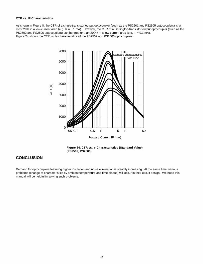
CTR vs. IF Characteristics
As shown in Figure 8, the CTR of a single-transistor output optocoupler (such as the PS2501 and PS2505 optocouplers) is atmost 20% in a low-current area (e.g. IF = 0.1 mA). However, the CTR of a Darlington-transistor output optocoupler (such as thePS2502 and PS2506 optocouplers) can be greater than 200% in a low-current area (e.g. IF = 0.1 mA).Figure 24 shows the CTR vs. IF characteristics of the PS2502 and PS2506 optocouplers.
Forward Current IF (mA)
CT
R (
%)
CONCLUSION
Demand for optocouplers featuring higher insulation and noise elimination is steadily increasing. At the same time, variousproblems (change of characteristics by ambient temperature and time elapse) will occur in their circuit design. We hope thismanual will be helpful in solving such problems.
Figure 24. CTR vs. IF Characteristics (Standard Value)(PS2502, PS2506)
7000
6000
5000
4000
3000
2000
1000
00.05 0.1 0.5 1 5 10 50
Standard characteristics VCE = 2V

33
APPLICATION OF AC INPUT COMPATIBLE OPTOCOUPLER
INTRODUCTION
With the rapid penetration and diversification of electronic systems, demand for optocouplers is strengthening. Most popular areproducts featuring compact design, low cost, and high added value.
To meet the market needs, NEC is expanding the optocoupler. This manual focuses on optocouplers compatible with AC input,and covers configuration, principles of operation, and application examples.
CONFIGURATION (INTERNAL PIN CONNECTION DIAGRAM)
Figure 1 shows the internal pin connection of the AC input compatible optocoupler PS2505-1, and Figure 2, of the optocouplerPS2501-1. The most significant difference from the optocoupler (PS2501-1) is that the PS2505-1 incorporates an input circuitwith two LEDs connected in reverse parallel. In the optocoupler (PS2501-1), one LED is connected in the input circuit so that theLED emits light to provide a signal when a current flows in one direction (1-2 in Figure 2) (one-direction input type).However, in the configuration shown in Figure 1, when a current flows in direction 1 to 2, LED1 emits light to send a signal, andwhen it flows from 2 to 1, LED2 emits light to send a signal (bidirectional input type). Namely, even if the voltage level between 1and 2 varies, and the positive and negative polarities are changed, either of two LEDs emits light to send a signal. This meansthat the one direction input optocoupler permits DC input only, while the bidirectional input type permits AC input as well. There-fore, the PS2505-1 is described as an AC input compatible optocoupler.The next section describes the status of output signals when 100 Vac power is directly input to an AC input compatibleoptocoupler (PS2505-1) via a current limit resistor.
Figure 1. PS2505-1 Figure 2. PS2501-1
1
2
4
3
(LED2) (LED1) 1
2
4
3

34
DIRECT INPUT OF 100 Vac
Figure 3 shows the circuit diagram when 100 Vac power is directly input to an AC input compatible optocoupler via a current limitresistor. The relationship between input and output signals is as shown in Figure 4.
+
0
_
+
0
LED 1LED 2
LED 1LED 2
LED 1LED 2
Deviation due tothe differences inlight emission andcoupling efficienciesof LEDs
Input signalAC 100 V
LED lightemission
output
Output signal
Graph 1 Upper: 100 Vac Input Signal 100 V/DIVLower: Output Signal 1 V/DIV
As described above, when an AC input compatible optocoupler is used, an AC input signal can be extracted as a full-waverectified output signal. The output signal is smoothed by inserting a capacitor in the last stage of the circuit of a phototransistor ifnecessary.
In the one-direction input optocoupler (PS2501 series), when an AC signal is to be input, it must be full-or half-wave rectified by adiode bridge or CR circuit. On the other hand, the AC input compatible optocoupler permits direct input of an AC signal. Thisenables simpler configuration, space saving, and reduced design cost.
The next section demonstrates three examples of applications.
Figure 4. Input/Output Signal
(LED2) (LED1)
PS2505-111 kΩ
AC 100 V
100 Ω
Output signal
VCC = 10 V
Figure 3. 100 Vac Direct Input Circuit

35
AC 100V
VCC
PS2505-1
+
0_
APPLICATION EXAMPLES
Example 1: AC-DC converter
AC 100 V
VCC
PS2501-1
+
0
+
0
(b) Conventional optocoupler (one-direction input) (Full-wave rectification by means of diode bridge)
Example 2: Detection of a telephone bell signal
PS2505-1
+
0
_
Station line(75 Vr.m.s., 16 HZ)
(a) AC input compatible optocoupler (bidirectional input)
(b) Conventional optocoupler (one-direction input) (rectification by CR circuit)
(a) AC input compatible optocoupler (bidirectional input)
Station line(75 Vr.m.s., 16 HZ)
PS2501-1
+
0
_
+
0
_

36
Example 3: Sequencer circuit input section
AC 100 VPS2505-2
Common
Common
PS2501-2
AC 100V
(a) AC input compatible optocoupler (bidirectional input)
(b) Conventional optocoupler (one-direction input) (Full-wave rectified by diode bridge)
PRECAUTIONS FOR DESIGN
The AC input compatible optocoupler is identical to the conventional optocoupler except for the presence of two LEDs connectedin reverse parallel in the input circuit. Therefore, the circuit configuration can be designed as conventionally. The difference isthat there are two types of current transfer ratios (CRT) because two LEDs are connected in the input circuit. The two CTRs arenot necessarily the same, owing to the differences in light emission and coupling efficiencies of LEDs. Consequently, this causesdeviation in output signal level. The differences are rated under the item of the current efficiency ratio (CTR1/CTR2) for electriccharacteristics.
Current transfer ratio (CTR1/CTR2)
IC1
CTR1 = IF1 x (current flowing in LED1)
IC2
CTR2 = IF2 x (current flowing in LED2)
A
IF1
A
A
IF2
LED 2 LED 1
IC1
IC2VCE = 5 V
Figure 5. CTR Measuring Circuit

37
ITEM CODE CONDITIONS MIN. TYP. MAX. UNIT
Forward voltage VF IF = ±10 mA 1.1 1.4 V
Pin-to-pin capacitance Ct V = 0, f = 1.0 MHZ 50 pF
Transistor Collector cutoff current ICEO VCE = 80 V, IF = 0 100 nA
Current transfer ratio CTR(IC/IF) IF = ± 5 mA 80 300 600 %VCE = 5.0 V
Collector saturation voltage VCE(sat) IF = ±10 mA 0.3 VIC = 2.0 mA
Insulation resistance R1-2 Vin-out = 1.0 kV 1011 Ω
Input-to-output capacitance C1-2 V = 0, f = 1.0 MHZ 0.5 pF
Coupled VCC = 10 V,Rise time tr IC = 2 mA, 3 µs
RL = 100Ω
VCC = 10 V,Fall time tf IC = 2 mA, 5 µs
RL = 100Ω
IF = 5 mA,Transfer efficiency ratio CTR1/CTR2 VCE = 5.0 V 0.3 1.0 3.0
The transfer efficiency ratio (CTR1/CTR2) is rated as 0.3 (MIN.), 1.0 (TYP.), and 3.0 (MAX.). Assuming that CTR1 is 200%, CTR2
is in the range of 66 to 600%. Therefore, an AC input compatible optocoupler should be designed to operate with CTR 66 to600%. For reference, the electric characteristics of the AC input compatible optocoupler (PS2505 series) are as follows:
Electric Characteristics (TA = 25°C)
For the external drawing, absolute maximum ratings, and characteristics curves, refer to the specific documents (AC inputcompatible multi-optocoupler series).
Diode
EXCLUSIVE NORTH AMERICAN AGENT FOR RF, MICROWAVE & OPTOELECTRONIC SEMICONDUCTORS CALIFORNIA EASTERN LABORATORIES • Headquarters • 4590 Patrick Henry Drive • Santa Clara, CA 95054-1817 • (408) 988-3500 • Telex 34-6393 • FAX (408) 988-0279
24-Hour Fax-On-Demand: 800-390-3232 (U.S. and Canada only) • Internet: http://WWW.CEL.COM
07/17/2000DATA SUBJECT TO CHANGE WITHOUT NOTICE

This datasheet has been downloaded from:
www.DatasheetCatalog.com
Datasheets for electronic components.