optoelectronics in focus – a market overview new
TRANSCRIPT

Optoelectronics in Focus –a Market Overview
New Dimensions in SiGe
Unaxis Semiconductors wins the Award
7

Front CoverProcess resultsobtained on aMASK ETCHER™ IIIsystem (bottom left)are analyzed in the UnaxisSemiconductorLab.
Editor in ChiefJuerg Steinmann,Global CommunicationsManager UnaxisSemiconductors
Managing EditorVeronika Schreyer, is design
Design /LayoutCactus AG
PhotographyMichael Reinhard ,Richard Steinmetzand Unaxis, unlessstated otherwise
Published byUnaxis SemiconductorsP.O. Box 1000FL-9496 Balzers Liechtenstein
Printed bySüdostschweiz Print AG
If you have any questions or comments,please contact us at [email protected] or faxthe reply card provided in this magazine.
Chip, the Business & Technical News from Unaxis Semiconductors,is also available on-line:
www.semiconductors.unaxis.com

Dr. Martin Bader, Executive Vice President, Unaxis Semiconductorsand President Unaxis North America
Dr. Martin Baderedito
rial
edito
rial
Unaxis Chip
Hello and welcome to Chip 7!
Slowly the clouds are lifting that have dimmed the Semiconductor sky during the last fifteen
months, and the first rays of economic sunshine have begun to penetrate – and we are all hopeful
that we will not face a “double dip”. Although the market recovery is still below expectations,
Unaxis Semiconductors is well prepared for the upswing.
Our intensive investments in R&D and the efforts to improve our products and services are
beginning to pay off: The 300 mm CLUSTERLINE® that we introduced last year has been well
received in the market – the right product at the right time. For many of our customers the 300
mm market is now the way to go as yields and throughput are becoming equal to the best
200 mm processes. The potential to reduce production cost by nearly 30% is certainly a hard
driver. In 2002, 300 mm fab construction should exceed 200 mm for the first time.
Optoelectronics is the technology focus of Chip 7, beginning with an introductory market
overview on page 8.
SiGe: In our last issue we presented the extension of the CLUSTERLINE® 300 concept for Low
Energy Plasma Processing (LEPP). The story continues in this issue with the highly interesting first
results of the LEPP process development (p. 38).
In the Advanced Packaging market a novel technique has been developed making use of
highly stressed thin films (p. 44). This is an unusual development, as in most cases the goal is to
keep stress as low as possible in order to provide durable and reliable film stacks.
Even the most innovative company will not reach its full potential without a strong commitment
to customer focused business processes. Unaxis has increased its efforts towards Business
Excellence and it shows: In June 2002 Unaxis Semiconductors was awarded the VLSI 10 BEST
Award in the category of Semiconductor Equipment Suppliers.
The ISO 9001 re-certification took place in February in Truebbach, and St. Petersburg will be
certified in the beginning of 2003.
Please contact us if you require further information on one of the topics or Unaxis Semicon-
ductors in general. I hope you will enjoy reading this new edition of Chip and we are looking
forward to your feedback on [email protected].

Chip Unaxis
cont
ents
cont
ents
Unaxis InsightsGlobal Account ManagementCustomer Service – Worldwide 4Magneto Electronics Has MovedA new lab and state-of-the-art equipment close to the customer 6Unaxis Community 7Events 49
FeatureSeeing the LightOptoelectronics market focus: forecast for optical componentsin telecommunications networks 8
TelecomWhat’s Next in Telecom 13DWDM – Lightwave Connection to the Data HighwaySilica-Planar Lightwave Circuits (PLC) for telecommunications 14Ion Plating: Optoelectronics at the CrossroadsThe new GSM 1100 optical monitoring system 18Wireless Future with BAWBulk acoustic wave (BAW) devices – promising technology for future wireless communications 22Optimized Sputter Sources for LLS EVO 27A Higher Etch Rate with GaAs Via Etch IIISignificantly increased throughput while maintaining profile control 29
627
Superb cleanroomfacilities have been installed in the St.PetersburgLab.
Double targetlifetime, reducedmaintenance,increased yield – the new LLS EVOdelivers excellentperformance.

Unaxis Chip
cont
ents
cont
ents
42Unaxis Semiconductors’MASK ETCHER™ III is now demonstrating 90 nm process specifications.
Advanced SiliconThe Future of SiGe Beyond HBT ApplicationsWill the heterostructure field-effect transistor (HFET) be theleading device in the race towards higher speeds? 32Differential Growth by UHV-CVDAchieving selectivity for growth processes at lower temperatures 36LEPP 300 – SiGe Process DevelopmentPart I 38MASK ETCHER IV – the Answer to NewLithography Trends 42
Advanced PackagingNanosprings – New Dimensions in SputteringStressed metal nanosprings – a cooperation between PARC and Unaxis Semiconductors 44APiA Builds MomentumNotes from the APiA seminar at Semicon Europa 2002 48
44Stressed metalnanosprings: Out-of-plane microinductorsintegrated with activecircuitry
38LEPP 300beta-sitesystem

4 | Chip Unaxis
Global Account ManagementCustomer Service – Worldwide
Nicole Lippuner, Marketing Communications, Ralf Kuhlmann, International Sales and Market Manager Unaxis SemiconductorsDr. Christoph Senn, Senior Lecturer for International Management, ResearchInstitute for International Management, University of St.Gallen/Switzerland, and Founding Partner AMC Account Management Center AG, Zürich
Unaxis Insights
In order to help avoid costly trial-and-error experiences, the University of St.Gallen (Switzerland), Columbia Business School (New York, USA), and the Account Management Center (Zurich, Switzerland) have created theGAMBIT (Global Account ManagementBenchmarking for InternationalCompanies) project. It offers its participants the opportunity to explorecurrent successful practices and thefuture challenges of global accountmanagement. Dr. Christoph Senn,founding partner of the AccountManagement Center, is convinced:“Concentrating forces on globalcustomers is neither magic nor rocketscience – it is simply a permanent learning process!”
The GAMBIT project is split into threephases lasting over 18 months and itdelivers continuous results by using thesystematic “Nine-Field-Model” (Figure 1),which has been successfully validated inover thirty international companies.
Figure 2 shows previous researchresults of the University of St.Gallen.Sucessful GAM programs require not
More and more global customers requirebusiness solutions to be implemented and managed consistently across theirworldwide locations. Supplier relationshipprograms require best-in-class support in all areas, from support services tocontracts and pricing. Knowledge ofglobal spending levels is mandatory as well as the management of theserelationships on a centralized, coordinatedbasis. Therefore, many firms havereduced their supplier base dramatically inrecent years, and this trend is continuing.
Ralf Kuhlmann explains: “Achieving and maintaining world-class customer-supplier relationships is a complex task. It goes well beyond the many customerrelationship management initiatives in worldwide industries. Unaxis Semiconductors has decided tostrengthen its global business model by introducing a GAM (Global AccountManagement) program.”
“Concentrating forces on global customers is neithermagic nor rocket science – it simply is a permanentlearning process!”
Dr. Christoph Senn

Unaxis Chip | 5
“The whole program will help us to continuously improveand be more creative in serving our customers.”
Ralf Kuhlmann
Unaxis Insights
The “Nine-Field-Model” (9FM)
Resource Allocation Standardization Knowledge Sharing
CRM
Target definitionsUnaxis Semiconductors
Research Institute for International Management, University of St.Gallen
Synergies
Network
Customers Relations Knowledge
Set Objectivesand Strategies
Align OrganisationStructures
AccelerateInformation Flow
Solutions Processes Systems
People Structures Information
Figure 2: Successfulcompanies show anoutstanding scale of values within theentire project scope.Based on a detailedSWOT analysis theCockpit* monitorvisualizes theeffectiveness ofinitiated action plans.The improvementresults are continuouslybenchmarked against the best-in-class performers in each category and on a globaldatabase.
only good relationships and qualified salesstaff, but also must concentrate on manyadditional factors. World-class companiesshow peak values in all elements of theirGAM-programs while orchestrating theiractivities cautiously and consequently at the same time.
Ralf Kuhlmann: “The GAMBIT projectenables us to continuously put our GAM practice to the test. Joining thebenchmark consortium of members withmutual interests will result in a continuousflow of research results which will bechallenged in conjunction with pragmaticaction plans. Our main focus at UnaxisSemiconductors is to build and maintainbest-in-class customer relationships andidentify growth areas in line with our globalkey accounts prospects based on ourdivision strategy.”
In a nutshell, the GAMBIT conceptmeans that a limited number of non-competing companies enter a highlyefficient and fast learning process incooperation with leading subject expertsand research institutions. Dr. ChristophSenn explains what the project can do for Unaxis Semiconductors: “The GAMBITproject provides Unaxis with the uniqueopportunity to combine traditionalbenchmarking efforts with organizationallearning activities.”
The project will last from Spring of 2002until Fall of 2003 and is divided into threephases:
1: GAM assessment with results in thedevelopment of individual action plans.
2: Comparison of member performancewith world-class examples in similarmarket segments.
3: Best practice case studies will serve asvaluable sources of innovative ideas.
(sp) Supplier Performance (n=38)(cp) Customer Performance (n=22)
© 2000 Account Management Center
People Structures Information
Solutions Processes Systems
Customers Relationships Knowledge
Organization level
Functional level
Strategic level
0% 100% 0% 100% 0% 100%
0% 100% 0% 100% 0% 100%
0% 100% 0% 100% 0% 100%
65% (sp) 75% (cp) 76% (sp) 80% (cp) 66% (sp) 70% (cp)
56% (sp) 67% (cp) 53% (sp) 62% (cp) 46% (sp) 60% (cp)
69% (sp) 77% (cp) 55% (sp) 67% (cp) 65% (sp) 81% (cp)
Figure 1: Research shows that successfulGAM programs do not only require “good”relationship managementor the “superhuman” sales professionals. Onthe contrary, companiesperforming an integratedview on all areas of the“Nine-Field-Model” wereable to achieve 20 –30%higher customersatisfaction ratings.
*Screenshot of a 9FM GAM cockpit produced with the software AMC Conductor™, © AMC Account Management Center AG, 2002. All rights reserved.
Account Management Center™

6 | Chip Unaxis
Unaxis InsightsUnaxis Insights
With the acquisition of Plasma-Therm in theSpring of 2000, Unaxis added plasma CVDand plasma etch expertise and products inthe field of magneto electronic applicationsto its product portfolio. Having a teamfocused on sputtering and ion beamdeposition (IBD) in Alzenau (Germany) and a team working on plasma CVD and dryetch in St.Petersburg (Florida), the newMagneto Electronics Business Unit beganutilizing its acquired depth of technology to
offer combined processes, e.g. GMR/TMRdeposition and etch.
In an effort to improve the efficiency of the Business Unit, the consolidation of both groups to one location was thenext logical step. The physical transfer of the PVD and IBD businesses fromAlzenau to St.Peterburg created the following customer benefits: Customer and market proximity R&D and demonstration capabilities
Magneto Electronics Has MovedRudolf Koetter, Design Engineering Manager Peter Wohlfahrt, Program Manager, Magneto Electronics
in the newly opened R&D Class 100cleanroom facilities (Figure 2)
Systems production in a cleanroomenvironment (Figure 1)
One site to coordinate businessprocesses
The challenging part of this project was inreducing the risk of technology losses anddemonstrating continuity to the market.
To do this, a core team across theorganization moved from Germany toFlorida. The integration of these personnelinto the St.Petersburg organization and a technology transfer program withnumerous training sessions in Alzenauand St.Petersburg was the stepping stone for success.
In the field of R&D, we enhanced ourmagnetic and sputter expertise andextended our team through additionalhiring. With regards to supply chainmanagement, we have already benefitedfrom outsourcing during previous years.Furthermore, it was essential to realizeinterruption minimized sampling andsystem demonstration capabilities. Themovement of CORONA® and CYBERITE®
systems, including the metrology into thefirst class cleanroom facilities is complete.The first samples went to customer sitesin the first quarter of 2002.
The aforementioned steps bring us tothe advantageous situation of being theone stop shop for integrated product andprocess solutions in our targeted marketplaces: Thin Film Heads MRAM Planar Optics
For more information please contact:[email protected]
Unaxis Insights
Figure 1: UnaxisSemiconductors’state-of-the-artmanufacturing floorin St.Petersburg,Florida
Figure 2: R&D lab with CORONA® andCYBERITE® systems in the Class 100 Clean-room facilities

Unaxis Chip | 7
Unaxis Insights
Unaxis has been in the business oftechnology and the manufacturing oftechnology since Ernst Leybold andWilhelm Carl Heraeus founded Leybold-Heraeus in the mid 1800’s. Their visioncontinued through the Balzers technologyand today with Unaxis. In the fall of 2001,Unaxis USA, Inc. joined three localcolleges – Hillsborough CommunityCollege, St. Petersburg College and theUniversity of South Florida – in proposinga regional center for manufacturingeducation.
In late April 2002, the National ScienceFoundation of America granted $50,000to pay for a yearlong study to assess the workforce and educational needs of area manufacturers. The results of the study could win grants of up to $350,000 a year for three to five years to setup and operate the center, dubbedthe “Greater Tampa Bay Regional Centerfor Manufacturing,” by Carlos Soto, president of Hillsborough Community
College’s Brandon campus. The Centerwill address the educational needs of themany high tech manufacturing facilities in the region and undertake educationmaterial development, perform adaptationand implementation activities and fosterprofessional development for educatorsbased on regional industry needs.
“We feel very strongly that we need tobuild a more structured base of peopletrained in manufacturing skills,” said Dr. Wayne Pasco, COO Unaxis USA. “We look forward to participating with an organization that can create and facilitatean optimal high tech manufacturingeducational delivery system to develop andenhance its workforce”, Wayne continued.
Mayor’s CornerThe City of St.Petersburg is a strongsupporter of technology companies. “I view technology as one of the threemost important economic underpinnings
of our area,” said Mayor Rick Baker.“Along with the growing financial centersand tourism, technology will be the key to our future.”
Unaxis USA is actively participating withthe Mayor’s technology thrust. A regularmember of the Technology Council,Unaxis supports initiatives in education,supplier development, and local andregional governmental actions to enhanceand grow high tech opportunities.
“We hosted the Mayor and his staff hereat Unaxis on June 20th,” says WaynePasco. “This is part of our ongoinginteraction with our local government to ensure full understanding and buildcooperative efforts to advance ourposition as a technology leader and ourstanding in the community.”
Unaxis USA will continue to participatein local and regional activities as part ofthe company’s overall BusinessExcellence commitment.
Unaxis Community –Textbooks to Technology
“I view technology as one of the threemost important economic underpinningsof our area”
Rick Baker, Major of St.Petersburg
Outside UnaxisSemiconductors, St.Petersburg,Florida (from left to right): Mike Archuletta,Frederic van Mullem,Teresa Brydon, LynnOchs, Wayne Pasco, Rick Baker, Mayor of St.Petersburg,Max Schaelchli,Cindy Margiotta, and Marion Turner
Visiting the Class1000 manufacturingtest area (from left to right):Jeff Stockdale, the Mayor, CindyMargiotta, andTeresa Brydon
Marion Turner, U.S. Marketing Communications Manager

The cost saving and performance-boosting nature of planar waveguidecircuits made from fairly standardsemiconductor materials is an importantplatform for the next wave of growth intelecommunication networks.
Long haul and metro infrastructure, theprofessed core networks, have adoptedfiber optics because the technologydelivers a huge improvement, in terms of speed, cost, and maintenance, over the legacy networking systems it replaces.The industry expects the conversion of existing electronic, copper-wiredinfrastructure of access networks to be next.
If the so-called last mile is to undergo a fiberoptic upgrade, then the cost ofconnecting office buildings, premises, andhomes located in that last mile to themetro and core networks has to decreaseby a dramatic 90% of what it is today.
It is generally agreed the only way toachieve this kind of shift in costs is to usesemiconductor manufacturing processes,packaging, design, and integrationtechniques to make optical devices.
The evolution from customized,expensive, handmade optical componentsto mass-produced ones, at a much lowercost, has already begun.
State of the optical telecommunications artA number of optoelectronics manufacturers are already using semiconductor deposition processes to fabricate planar opticalcomponents. Early adopters say they can cut costs, improve yields, and
Seeing the lightOptoelectronics Market Focus
Valerie Thomson, Technical Journalist, Zurich
Up-to-the-minute sales forecasts for optical components, with a focus on planarwaveguide circuits and their importance intelecommunications networks.
Feature

Unaxis Chip | 9
hike reliability of devices such as planarlightwave circuits and arrayed waveguidegratings (AWG).
Semiconductor processing techniquesare used to define the waveguides, as well as the pits, grooves, and markersneeded to align other components withthe waveguides in “hybrid” planarlightwave circuits, which are based on a wafer subassembly.
Some components, including thewaveguides themselves, can be fabricateddirectly on the wafer. Others, like lasers, sitin holes etched out of the wafer.
AWGs are the first high-growth optical components to adopt planartechnology. In an article about LightwaveMicrosystems, Light Reading, a tradepublication for the optical networkingindustry, says that its AWGs are “not fanciful next-generation widgetswaiting for the advent of new networkarchitectures, but established
components that have already stolensignificant market share away from theincumbent technology, thin-film filters.”
AWGs, however, represent just thebeginning. Planar lightwave circuittechnology is generally believed to be thebasic building block in the movementtoward the optical equivalent of theelectronic integrated circuit.
Next in line are things like dynamicallyreconfigurable gain equalizers, adaptivechromatic dispersion compensators,reconfigurable wave division multiplexingadd-drop filters, WDM multiplexers anddemultiplexers, as well as optical switches.
Industrial rolloutsThe rollout of foundry capacity ready to exploit the market opportunity has not halted, despite the recent plunge in optical sub-system equipment sales due to the economic downturn that began in 2000.
In the past few months, Intel Photonics,a new division of the semiconductor giant,announced its plan to offer planarlightwave circuits using its own siliconwafer manufacturing expertise.
Alcatel Optronics acquired Kymata, a pioneer in the development of PLCs,and is expanding its wafer manufacturinglines. Wavesplitter, along with OMD in theUK, announced new planar lightwavecircuit foundry services.
“Certainly the industry does not needsuch abundant manufacturing capacitytoday,” says Sheridan Nye of RHK, atelecommunications market research firm. Nevertheless, these developmentsshow how the key players are investing in their technologies and manufacturingcapabilities in anticipation of the expectedmarket upturn in 2003. (For a furtherdiscussion of the complexion of themarket, see “Market Snapshot andForecasts.”)
The know-how to successfully fabricatewafers for optical networking applicationsis rare. For that reason, some of the verylarge networking equipment vendors aretaking over startups that are successfullydeploying the technology.
For example, JDS Uniphase justacquired Scion, a company that makesvariable optical attenuator arrays andother integrated optical componentdevices. Scion has boasted about itssuccessful fabrication of eight-inch wafers with a yield of 50 dice per wafer.Industry observers say this is a dramaticimprovement over competitors, such as NTT Electronics Corp and OpticalMicro Devices.
“JDS already makes AWGs, but theacquisition of Scion to replace its existingoperation suggests it needs to improve
Figure 1: Growth ofphotonic integratedcircuit subsystemand components
2,000 4,000 6,000 8,000 10,000
4,059.6
9,470.3
260.6
1,514.0
AAGR* 2001 – 2006
AAGR 2001 – 2006
AAGR 2001 – 2006
+ 18.5%
+ 42.1%
+ 20.5%
Integrated opticalcircuits (discrete
components)
Integrated circuits(subsystems)
4,320.2
10,984.3
TOTAL
0
Market in Million $
* Average annual growth rate
20012006
Source: BCC
Feature

10 | Chip Unaxis
its existing devices and manufacturingprocesses,” writes RHK in a presscommentary.
In addition, venture capital investors are putting money into newcomers whoclaim to have planar optical expertise. InMarch, 2002, Neo Photonics Corporationreceived venture capital funding to thetune of $ 25 million to develop its planaroptical devices.
Feature
In Europe, Scottish Terahertz PhotonicsLtd. secured $ 8.8 million to develop its planar lightwave circuit platformtechnology last month and French silica-on-silicon planar circuit makerOpsiTech raised $ 6 million last fall.
Industry analysts and investors believethat companies such as Nortel Networks,Lucent, Alcatel, and JDS Uniphase and thedozens of optical networking component
Figure 2: ElectroniCast’soptical componentmarket forecast
Integrated circuits(ASICs)
Dynamic gain equalizers
Isolators
Optoelectronictransmitter/receivers
Plus related test unitsPlanar waveguide
circuits
Couplers
Optical fiberamplifiers
Variable opticalattenuators (EVOAs)
Integrated circuits(ASICs)
Dynamic gain equalizers
Isolators
Optoelectronictransmitter/receivers
Plus related test unitsPlanar waveguide
circuits
Couplers
Optical fiberamplifiers
Variable opticalattenuators (EVOAs)
2000 2006
9,732 M $ 47,624 M $
Table 1: ElectroniCast planar waveguides circuits global consumption marketforecast, by region (Value Basis)
2001 2006 2011
Japan/Pacific Rim
ROW
North America
Europe
Total
Source: ElectroniCast
28%
–
48%
24%
100% = 173.2 M $
29%
1
49%
21%
100% = 813.1 M $
30%
2
45%
23%
100% = 4’223 M $
startups will begin to outsource the early wafer processing steps. Specialistfoundries or contract manufacturers areable to produce planar lightwave circuits in volume with greater efficiency and costsavings.
Evolution towards integrated opticsOptical networking analyst LawrenceGasman from Communications IndustryResearchers, Inc. believes that integratedoptics “holds great promise for the futureof optical components.”
Made from one material (or a smallsubset of compatible materials), photonicsintegrated circuits have no mechanicaljoins or bonds between different sections of the chip. The component is manufactured from start to finish using a linear sequence of processes.
The benefits of putting multiple optical functions on the same piece of

Unaxis Chip | 11Unaxis Chip | 11
It wasn't that long ago when the optical networking industry wascomplaining about shortages of optical components. From the Fall of1999 to the Spring of 2001, there was a surge in demand from systemsvendors that seemingly couldn't get the product out fast enough.
Then the growth figures began to hit a speed bump and fall into a slump.Now, the telecommunications industry has seen four consecutivequarters of double-digit declines, which has without a doubt affected the component suppliers too.
Of a dozen long-haul carriers in North America who were all buildingnetworks, there are now only six – Williams being the latest. NowWorldcom, Cable &Wireless are threatened as well.
After seeing the optical components market experience 130% growth in 2000, RHK, a market research firm, predicted 90% growth in 2001. It forecasted the optical components market for dense wave divisionmultiplexing applications would reach $ 9.5 billion in 2001, and soar to$ 23.6 billion by 2004.
It recently had to downgrade its growth figures and now says the marketfor components will drop from about $ 5 billion in 2001 to around $ 2.6billion this year. For 2003, the market should grow to somewhere closeto $ 3 billion, says RHK.
CIBC World Markets’ analysts say optical component revenues areexpected to decrease 41% in 2002 from 2001.
Analysts at Strategies Unlimited are even more conservative, believingthat capital spending among carriers will decline 21% by the end of2002, which will drive down "optical component revenues by 60% from 2001 levels”.
Most analysts are predicting a soft recovery in 2003. Growth rates of 30 to 90% won’t be happening again soon. The consensus is 8 to 12%growth.
Growth seen in 2002 for metro components
One bright spot for 2002 is the AWG sector. AWGs are a key buildingblock for Optical Add/Drop Multiplexer components and subsystems – a market which is expected to grow at an average annual rate of 52% from 2002 to 2006, according to Communications IndustryResearchers, Inc. (CIR).
CIR says that $ 27.5 million worth of AWGs were shipped in 2001 and it forecasts that by 2005, AWG shipments will top $ 192.7 million.
According to telecommunications market research firm ElectroniCast,the consumption of planar waveguide circuits, of which AWGs are asub-category, is to grow from $ 173 million in 2001 to over $ 4.2 billion by 2011.
Market Snapshot and Forecasts
Feature
semiconductor are well known and there is still much R&D to be done todiminish obstacles.
Since the introduction of photonicsintegrated circuits in 1997, the opticalcomponent industry has slowly beenmigrating from the manual assembly ofdiscrete optical devices to automated,semiconductor wafer processingtechniques and single-chip solutions.
The photonics industry has yet topublish a series of roadmaps to expeditethe evolution of a photonics integratedcircuit market. Therefore, it is stillconsidered an emerging market. Demand for photonic chips will blossom in 2003, according to BCC. “At that time,simultaneous upgrades in both networkarchitecture and bandwidth – specificallythe all-optical and 40-Gbps networks –will establish sizeable end markets for advanced optical components,” says BCC’s analyst.
Next-generation devices are predominately based on chiparchitectures, according to BCC.
Market research firm RHK says themarket potential for integrated opticalcomponents will be $ 675 million in 2005.According to BCC, the future is a bit rosierthan RHK thinks and says that by 2006photonics integrated circuits subsystemswill generate $ 1.5 billion in sales.
Other market research firms suggest itmay be a bit later, but all agree thephotonics chips are coming soon.
Downturn drives optoelectronicintegrationWith their eyes on the access market, anumber of startups are working hard toreduce the cost of components by usingplanar waveguide technology, as well
Valerie ThompsonMSc., has been a freelance business andhigh-tech writer formore than 10 years. A Canadian based in Zurich, she tracks the trends and developments of Europe’s purveyors ofadvanced technology.
Figure 3: Photon*PCSS™ from LynxPhotonics is an integrated subsystembased on planar lightwave circuit(PLC) technology. Shown here is anoptical chip module with electroniccontrol plane mounted on a samplevertically mounted system. The flatblack module contains the PLC chip.
as adopting other techniques for thesemiconductor manufacturing industry.
Ultimately, firms that can survive and be ready to offer the equipment, supplies,and services required for the next phaseof the optical market development, will bein a position to benefit from the marketdevelopment.
If anything, the downturn has putpressure on the optical networkingindustry to improve productivity, cutcomponent costs, and any other aspectsof the supply chain that have beenoperating inefficiently. This cost-cuttingtrend could prove to be a greatopportunity for the semiconductorindustry to play a role in makingcomponents less expensive. If the costsof components drop as dramatically as they have the potential to do usingsemiconductor know-how, this could lead to a new boom in the opticalnetworking market, say the analysts. A boom that will perhaps include anumber of today’s semiconductor giants.

12 | Chip Unaxis
Class 100 R&D lab for development andsampling of the latesttelecommunicationsdevices

Unaxis Chip | 13
Definitely one of the most promisingcandidates for future growth and forchallenging technology developments is the telecommunications industry.
While areas like data storage and datafarming will be growing in one-digit areas over the next few years, digitalcommunication – especially when itcomes to broadband and ultra broadbandwidth – have an annual growth factor of15% and higher.
However, the industry is young orshould I say, has a “young” image, and isfacing its first roadblock. While the long-haul communication lines are alreadyunderground and metro connections arealmost complete, connections andaccess to these lines as well as theconnection to the individual householdsand small communication units seems tobe bottlenecking. New technologies areeither too expensive or uncompetitive withregard to performance and cost oftraditional communication technologies.
One way to increase the performanceand yield of these new connections is ahigher degree of integration. Another isthe usage of already existing technologyin the Si semiconductor arena. Using a phrase out of the traditional precisionoptics, planar optics in this new technologymeans highly precise optical layers orlayer systems on Si wafers. Other than in classical optics, the light is directedparallel to the wafer surface, furthering the integration of several opticalcomponents and functions that take place on the Si wafer.
During the last telecom boom two years ago, it was expected that the ultrabandwidth (“always-on”) would be donewithin 12 to 18 months. The reality hasshown another schedule and has openedthe window for new developments. The UMTS or G3 developments andmarket entries are the most prominentexamples for the faith in this industry. This kind of communication is in theworks, but it will take longer and moreeffort to reduce costs while increasingperformance.
Focusing on the area of Silica basedmultiplexer, de-multiplexer, as well as optical add and drop modules, Unaxishas made major developments over the last 12 months (see p. 14, “DWDM –Lightwave Connection to the DataHighway”). Initial market forecasts areneeded for new process equipment in the order of 200 to 400 thin filmprocess modules.
With the planar optics industry still in a very young stage, current devices are mostly handpicked and manuallyassembled. The industry is highly
diversified, with competitors dealing with each other and OEM and verticalintegrated manufacturers supporting eachother. As demonstrated in the magneticdata storage industry several years ago,the tremendous consolidation race willcontinue to accelerate.
In order to streamline Unaxis Semiconductors’ activities, a workshop toassess the current market situation as wellas develop new strategies was recentlyheld in Maarsen, Netherlands. Furtherworkshops will be held in the US and Asiain the upcoming months.
Even with the current market state and investments on hold, it will not be aquestion of “if” this market will pick up, it’s just a question of “when”.
Unaxis Semiconductors has positioneditself for when the market picks up andintends to be among the first to cross thefinish line.
Fore more information please contact:[email protected]
What’s Next in Telecom:Running the Last MileNotker Kling, Vice President TelecomThomas Beens, Sales & Service Manager,North-East Europe
Telecom
SiO2 Si InP MEMS
Discrete Excellent Good Poor Goodperformance (high fiber-coupling loss)
Integration Passive Monolithic /Hybrid Monolithic /Hybrid Monolithic /Hybrid Hybrid Active Hybrid Hybrid Hybrid Hybrid
Technology Mature Mature In development, In development,maturity except lasers /receivers except switches
Main cost Packaging Packaging Packaging Complexitydrivers loss performance wafer fabrication costs
Current Thermal Waveguide loss, Fiber-coupling loss, Optical path lengthissues management thermal management, wafer yield and cost in free space, scalability
fiber-coupling loss
Source: Photonics Spectra, February 2002
Table 1: Technologycomparison
Telecom

14 | Chip Unaxis
In the age of Information Technology,lightwave communications is key tohandling the bandwidth necessary tosupport the escalating demands for voice,data, internet, and video transmission.Currently at the telecom wavelength of 1.55 micron, the data transmission rate through an optical fiber is typicallyeither 2.5 or 10 Gbits/sec. By transmittingthe data over several tightly spacedwavelengths (or channels) in the 1.55micron regime, it is possible to reachmuch higher transmission rates. This isthe principle behind dense wavelengthdivision multiplexing (DWDM). There arethree types of DWDM systems: bulkoptics (thin film filters, bulk gratings),planar lightwave circuits (arrayedwaveguides), and fiber devices (Bragggratings) [1].
This article presents work on silica(SiO2)-based planar lightwave circuits(PLC) on silicon; In particular, the processsolution and product offering for thefabrication of CVD silica arrayedwaveguides (AWG). CVD silica is an
ideal material for AWG and PLC in general,as its optical properties are well matchedto the (silica) fiber. Integration of theseoptical circuits opens up the possibility ofexploiting the mass productioncapabilities of Si semiconductorprocessing. In Figure 1, an illustration of an AWG is shown. Figure 2 is anexample of a DWDM system for long haultransmission incorporating AWGs. In thisexample, AWGs can be used not only
DWDM – Lightwave Connection to the Data Highway
Dr. Kenneth D. Mackenzie, Principal Scientist,Abdul Lateef, Applications Manager, James M. Klemm, Senior Applications Engineer,Magneto Electronics
λ1 + λ2 + λ3 + … + λn
λ1
λn
Array of waveguides
In Out
Figure 1: Illustrationshows the basicprinciple of an AWG.Example is a demultiplexer.
Long Distance
EDFA OADM
Addλ
Dropλ
MUX DEMUX
EDFA
AWG-based
Transfer capacity = n x [data transmission bit rate (Gb/s) per channel]
Transmitters Receivers
100 km
Laser Diodes
AWG AWG
Modλn
λ1 Mod
λ2 Mod
Rx
λx
Mod
Rx1
Rx2
Rxn
Fiber
Figure 2: DWDM system incorporating AWGs.The AWGs multiplex(MUX) and demultiplex(DEMUX) the datatransmitted over n channels. An erbiumdoped fiber amplifier(EDFA) boosts theoptical signals for longdistance transmission. A reconfigurable opticaladd/drop multiplexer(OADM) can also befabricated using AWGtechnology.
Telecom

Unaxis Chip | 15
waveguides, high-density plasma CVD(HDPCVD). HDPCVD not onlycompliments PECVD technology, but itcan be used for the entire waveguidefabrication process. Similar to PECVD, the HDPCVD depositions are done at aprocess temperature of ~350°C. HDPCVDis based on the Unaxis inductivelycoupled plasma (ICP) source technologydeveloped for dry etching. Figure 4 detailsthe essential features of the reactor. Withthe HDPCVD technology, the stringentrequirements for silica waveguide itemizedbelow can still be met:
High deposition rate Index and thickness uniformity Precise index control Low stress and low birefringence
as multiplexers and demultiplexers butalso in reconfigurable optical add/dropmultiplexers (OADM).
Figure 3 shows the process flow forsilica AWG fabrication. There are eightmain process steps. The deposition andetch process steps are marked in blue. All six steps can be accomplished utilizingprocess equipment offered by UnaxisSemiconductors. In Table 1, theequipment suite appropriate for eachprocess step is summarized. Silicadeposition and etching is done on theUnaxis VERSALOCK® productionplatform. The Cr deposition for hard mask and subsequent etching are donewith a CORONA® PVD system and aVERSALOCK® ICP etch system. In thefollowing sections, we will discuss thesilica AWG design and both thedeposition and etch process performancein reference to achieving the stringentrequirements for AWG.
Silica waveguide design & depositionrequirementsAs shown in Figure 3, the basic structureof the silica waveguide consists of three layers: an SiO2 lower cladding (~20 µm thick), a Ge or N-doped SiO2
core (~6 µm thick), and an SiO2 uppercladding (~20 µm thick). N or Ge dopingraises the index of the core. This ensuresvertical confinement of the light in thewaveguide. Depending on the waveguidedesign, the index difference between thecore and cladding can be as small as 0.01.
In Chip 4 [2], we discussed UnaxisSemiconductors’ high-rate PECVD batchprocess technology for silica waveguidefabrication. We have extended thisprocess capability and developed anadditional product offering for silica
Gas inlet 1 (O2, Ar)
2 MHzRF coil power
13.56 MHzRF chuck power
Wafer(heated)
Reactive ICPPlasma
Gas inlet 2(SiH4, GeH4)
~
~
Si wafer 1. CVD SiO2
lower clad2. CVD Ge-SiO2
or SiON core3. Sputter Crhard mask
4. Apply resist layer 5. Pattern resist 6. Dry etch Cr 7. Dry etch core 8. CVD SiO2
upper clad
Figure 3: Processflow for silica AWGfabrication
Figure 4: Schematicdiagram of a HDPCVDchamber for silicadeposition
Process step Unaxis product Technology
1. CVD SiO2 lower clad VERSALOCK® PECVD/HDPCVD
2. CVD Ge-SiO2 or SiON core VERSALOCK® PECVD/HDPCVD
3. Sputter Cr hard mask CORONA® PVD
6. Dry etch Cr hard mask VERSALOCK® ICP
7. Dry etch core VERSALOCK® ICP
8. CVD SiO2 upper clad VERSALOCK® PECVD/HDPCVD
Table 1: UnaxisSemiconductorssolutions for silicaAWG fabrication
Telecom

16 | Chip Unaxis
The deposition rate for HDPCVD is up to2000 Å /min. The thickness uniformityacross a 150 mm wafer is less than ±2%.Figure 5 shows an index uniformity mapfor HDPCVD silica on a 150 mm wafer.The index uniformity is ±0.014%. Similarto PECVD, index control for the core layercan be achieved by GeH4 doping. InFigure 6, some of the results for Ge-doped HDPCVD silica are presented.Stress induced birefringence is a veryimportant phenomenon in relation towaveguides. It can lead to an undesirablepolarization-dependent wavelength shiftin the AWG. Specialized techniques areused to limit this effect in the completedAWG structure [3]. Birefringencemeasurements made at a wavelength of1.55 microns on individual layers of bothHDPCVD and PECVD SiO2 compare well
Min: 1.4624Max: 1.4628Mean: 1.4626Range: ± 0.0002Uniformity: ± 0.014%
1.4626
1.4627
1.4627 1.46281.4624
1.46
1.47
1.48
1.49
1.50
0 0.05 0.1 0.15
Ref
ract
ive
ind
ex
GeH4/(GeH4+SiH4) ratio
Figure 5: Refractiveindex uniformity mapfor HDPCVD SiO2 ona 150 mm Si wafer.Index measurementswere made at 633 nmwith a prism coupler.
Figure 6: Refractiveindex of Ge-dopedHDPCVD SiO2 versusgas flow ratio. Indexmeasurements weremade at 633 nm witha prism coupler.
Figure 8a:Waveguide etchedinto a 4 micron thickcore layer withvertical sidewall
Gas inlet
2 MHzRF coil power
13.56 MHzRF chuck power
Wafer(He cooled)
Reactive ICPPlasma
~
~
Figure 7: Schematicdiagram of anInductively CoupledPlasma (ICP)chamber for silicaand chromiumetching.
Telecom

Unaxis Chip | 17
Figure 8b: Waveguide etched intoa 4 micron thick core layer with acontrolled sidewall angle
with that of thermally grown SiO2 of similarthickness. The birefringence is low and inthe 10-4 range.
The plasma chemistry for the HDPCVD process is SiH4, O2, and Ar. It is a nitrogen-free process unlike PECVD,which utilizes a chemistry of SiH4 andN2O. The incorporation of nitrogen in silicafilms in the form of N-H bonding cancontribute to absorption loss in the 1.55micron wavelength regime. Silica filmsprepared by HDPCVD are much denserthan PECVD films as evidenced by the low wet-etch rate of HDPCVD films inbuffered oxide etchant. In order to densifyPECVD films and reduce any significantN-H related absorption loss, an additionalprocess step consisting of a hightemperature anneal (~1200°C) is oftenrequired.
Waveguide definition: Dry etching in a VERSALOCK® ICP reactorFollowing the deposition of the dopedcore layer, the next step is the etching of the core to define the individualwaveguides of the AWG device. A deepoxide etch process is required to definethese waveguides. Typical etch depthrequirements are about 5 microns. Thisnecessitates the use of a chromium hardmask. A CORONA® PVD system is usedto deposit this layer. Photolithography isthen used to define the waveguide patternon a photoresist layer coated on top of thehard mask. The following are the essentialrequirements for the silica core dry etchprocess: High silica etch rate Sidewall angle control Excellent CD and thickness uniformity High selectivity to the hard mask
material
These requirements have beensuccessfully met utilizing an inductivelycoupled plasma (ICP) etch module on theVERSALOCK® platform. A schematicdiagram of this high-density plasmasource is shown in Figure 7. ICP etching of silica offers high etching rates (>3000 Å/min typical) with selectivity tothe chromium mask of greater than 40:1.The capability to independently control the ion flux (ICP power) and ion energy(bias power) combined with low pressureoperation, allows for better control of the etched sidewall angle. For someapplications a sloped rather than a verticalsidewall profile is desirable. As illustrated by the two different examples in Figure 8,sidewall geometry control can beachieved by adjusting the etch processparameters.
The silica core layer is patterned usingthe sacrificial chromium mask layer, whichis also patterned by ICP dry etching.Chromium is etched in a chlorine-basedchemistry and silica is etched in a fluorine-based chemistry. Again, high etch rateand selectivity to the photoresist mask are required. With ICP technology, it ispossible to achieve chromium etch ratesgreater than 400 Å/min along with
selectivity to the photoresist mask ofgreater than 2:1. The final step in theprocess is the deposition of the thickupper clad layer.
The ability to combine HDPCVD &PECVD silica deposition with ICP dry etchon a single platform allows UnaxisSemiconductors to offer an integratedsolution for silica PLC fabrication.
For more information please contact:[email protected] [email protected]
References1 S. V. Kartalopoulos: Introduction to DWDM
Technology: Data in a Rainbow, (IEEE Press,Piscataway, N.J. 2000)
2 K. D. Mackenzie and A. Lateef, “High RatePECVD for Silica Waveguide Fabrication”, Chip 4, Business & Technical News from UnaxisSemiconductors, February 2001, pp. 32 – 35
3 Fan Zhong, Farnaz Parhami, and J. G. Bornstein,“A comprehensive method to reduce PDW inArrayed-Waveguide Grating”, OSA Trends inOptics and Photonics 70, Optical FiberCommunication Conference, Technical Digest,Post Conference Edition (Optical Society ofAmerica, Washington DC, 2002), pp. 73 –75
Telecom
Wavelength [nm]
Ref
lect
ance
[%]
Anti-reflection coating
0
1
2
3
1000 1050 1100 1150 1200 1250 1300 1350 1400 1450 1500 1550 1600
18 | Chip Unaxis
Telecom
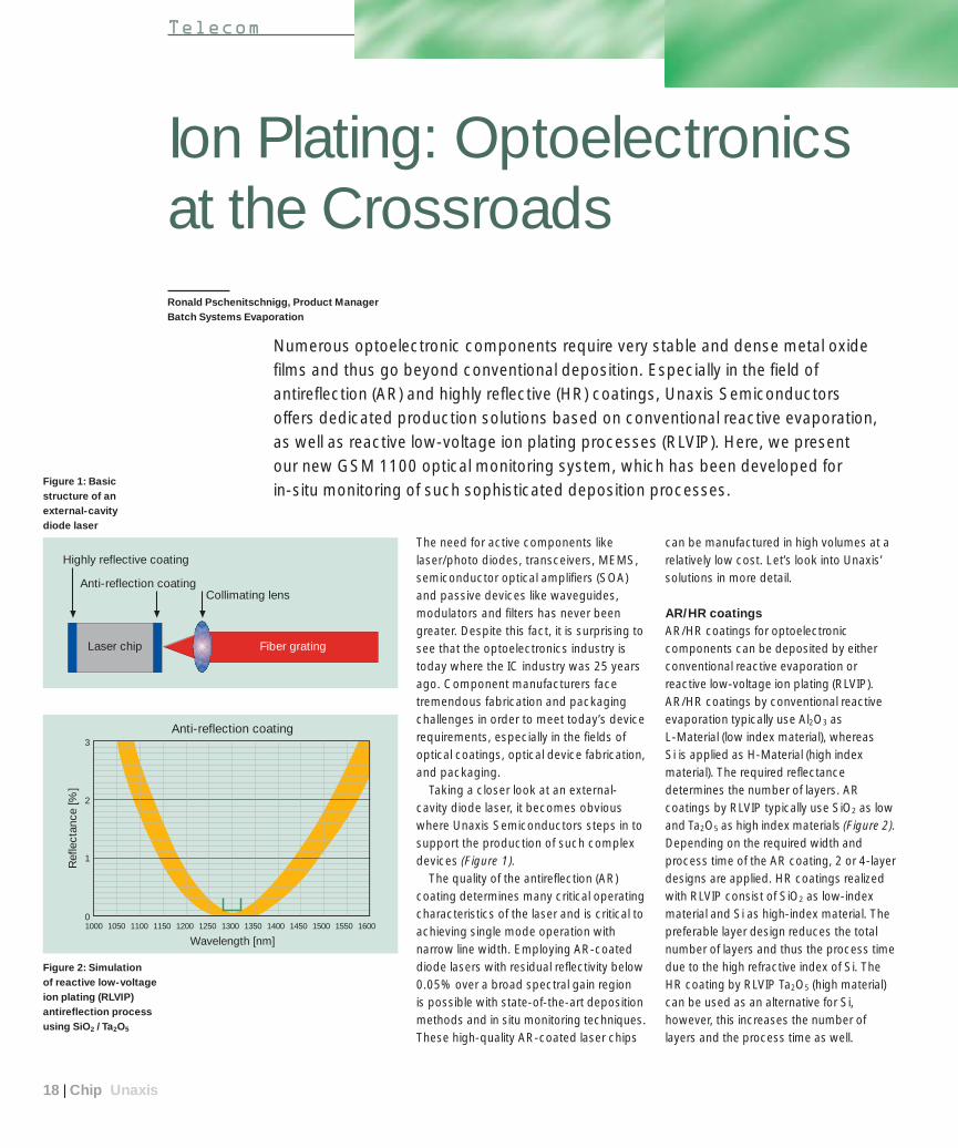
Ion Plating: Optoelectronics at the CrossroadsRonald Pschenitschnigg, Product ManagerBatch Systems Evaporation
The need for active components likelaser/photo diodes, transceivers, MEMS,semiconductor optical amplifiers (SOA)and passive devices like waveguides,modulators and filters has never beengreater. Despite this fact, it is surprising tosee that the optoelectronics industry istoday where the IC industry was 25 yearsago. Component manufacturers facetremendous fabrication and packagingchallenges in order to meet today’s devicerequirements, especially in the fields ofoptical coatings, optical device fabrication,and packaging.
Taking a closer look at an external-cavity diode laser, it becomes obviouswhere Unaxis Semiconductors steps in tosupport the production of such complexdevices (Figure 1).
The quality of the antireflection (AR)coating determines many critical operatingcharacteristics of the laser and is critical toachieving single mode operation withnarrow line width. Employing AR-coateddiode lasers with residual reflectivity below0.05% over a broad spectral gain region is possible with state-of-the-art depositionmethods and in situ monitoring techniques.These high-quality AR-coated laser chips
can be manufactured in high volumes at arelatively low cost. Let’s look into Unaxis’solutions in more detail.
AR/HR coatingsAR/HR coatings for optoelectroniccomponents can be deposited by eitherconventional reactive evaporation orreactive low-voltage ion plating (RLVIP).AR/HR coatings by conventional reactiveevaporation typically use Al2O3 as L-Material (low index material), whereas Si is applied as H-Material (high indexmaterial). The required reflectancedetermines the number of layers. ARcoatings by RLVIP typically use SiO2 as lowand Ta2O5 as high index materials (Figure 2).Depending on the required width andprocess time of the AR coating, 2 or 4-layerdesigns are applied. HR coatings realizedwith RLVIP consist of SiO2 as low-indexmaterial and Si as high-index material. Thepreferable layer design reduces the totalnumber of layers and thus the process timedue to the high refractive index of Si. TheHR coating by RLVIP Ta2O5 (high material)can be used as an alternative for Si,however, this increases the number oflayers and the process time as well.
Numerous optoelectronic components require very stable and dense metal oxidefilms and thus go beyond conventional deposition. Especially in the field of antireflection (AR) and highly reflective (HR) coatings, Unaxis Semiconductors offers dedicated production solutions based on conventional reactive evaporation,as well as reactive low-voltage ion plating processes (RLVIP). Here, we present our new GSM 1100 optical monitoring system, which has been developed for in-situ monitoring of such sophisticated deposition processes.
Figure 1: Basicstructure of anexternal-cavity diode laser
Figure 2: Simulation of reactive low-voltageion plating (RLVIP)antireflection processusing SiO2 /Ta2O5
Highly reflective coating
Anti-reflection coating
Laser chip Fiber grating
Collimating lens

Unaxis Chip | 19
Table 1 gives an overview of typicallyused materials and processes. Also, itbriefly describes which evaporation systemserves which purpose.
Depending on the required film qualityand the environment in which optoelec-tronic devices will be used, pastexperience has shown that RLVIP hasstrong advantages over conventionalevaporation. Let’s take a closer look whatRLVIP is all about and why this method is the one recommended by Unaxis.
The ion plating principleReactive low-voltage ion plating (RLVIP) is based on the standard method ofclassical evaporation under high vacuum(Figure 4). However, during the ion platingprocess a low-voltage, high-current arc isignited between a plasma source and the
crucible of a specially designed electron-beam evaporation source. The workinggas is usually Argon, whereas the reactivegas (e.g., O2, N2 for producing oxides byion plating) is admitted directly into thevacuum chamber.
During the coating process, the plasmagenerated in the vacuum chamber ionizesboth the evaporation material and thereactive gas. Atoms and molecules ionizedin this way are highly reactive. Also, the
Telecom
Table 1: Comparisonof RLVIP versusconventional reactiveevaporation, AR/HR in NIR (1300–1600 nm)
BAP 800 BAK EVO, BAK 640
Evaporation technology Reactive low-voltage ion plating Conventional reactive evaporation
Process leading Quartz crystal measurement QSK 621 or Quartz crystal measurement QSK 621 or
optical monitoring GSM 1100 optical monitoring GSM 1100
Evaporation materials SiO2 (low-index), Si, Ta2O5 (high-index) Al2O3 (low index), Si (high-index)
Evaporation sources ESQ 150 and ESQ 153 ESQ 212, ESQ 110, ESQ 113
electrically insulated substrate holderbecomes negatively charged in thepresence of the plasma. Finally, thepositively charged ions of the evaporationmaterial, the reactive gas, as well as theworking gas are accelerated towards the substrate holder. In other words, thisacceleration means they impinge on thesubstrates with high kinetic energy. In thisway, very dense, hard and adherent filmsare obtained even on unheated substrates.
Figure 3: Simulationof RLVIP AR processusing SiO2/Si
Figure 4: Ion Plating Principle: a) Substrate holderb) Electron beam
evaporation sourcec) Plasma Source

20 | Chip Unaxis
A plasma source is built into thevacuum chamber door in place of thelower sight glass.
Special electron-beam evaporationsources, the ESQ 150 and the ESQ 153,are modified versions of the standard ESQ110 and ESQ 113 sources (Figure 5).
The BAP 800 helps to improve existingthin film products and opens up entirelynew possibilities for thin film design. It isdedicated to semiconductors, transparentsubstrates, fiber-optics, optoelectronics,photonics, etc. especially in the fields of: Anti-reflection coatings Highly reflective coatings Stress compensation Short-pass filters Long-pass filters Cavity band pass filters
The new GSM 1100 optical filmthickness monitoring systemUnaxis has recently introduced its newGSM 1100, which has been developed to replace the industry-known GSM 420generation by a modular and robust state-of-the-art measurement system. One ofits key features is the full compatibility withthe previous GSM 420 system, meaningexisting GSM 420s can be replaced by anew GSM 1100. Also, all known featuresof the GSM 420 are incorporated in thenew GSM 1100.
The new GSM system concept is based on commercially available hardwarein order to keep design and functionsimple and reliable. The major difference
Depending on the composition of thereactive gas, ion plating produces oxides,nitrides and oxy-nitrides with excellentstructural properties, micro-hardness,abrasion and adhesion values as well aschemical stability.
Table 2 reviews the four most importantdifferences between conventional reactiveevaporation and ion plating processes(RLVIP).
In summary, ion plating coatings absorbvirtually no water because their density isvery close to that of the bulk materials. This particularly high packing densitycontributes to reproducibly high refractiveindexes, which display virtually no shift whenexposed to heat or moisture. Finally, themicro-hardness of ion plated films makesthem the ideal coating for substrateswhich will be exposed to harsh environ-mental conditions and/or mechanicalstress over longer periods of time.
Ion plated films generally come withcompressive stress, whereas evaporatedfilms often show tensile stressdevelopment. This is the reason why ionplating is used for stress compensation,which is required for many semiconductorapplications.
The BAP 800 ion plating evaporation systemThe Unaxis BAP 800 ion platingevaporation system is based on theindustry-known and field-proven BAKEVO (former BAK 760) evaporationsystem (Figure 6).
Figure 5: View inside the BAP 800 (ESQ150left, ESQ 153 right,front side – resistiveheated evaporationsources)
Figure 6: BAP 800 ionplating evaporationsystem
Telecom
Item * Criteria Conventional Processes Ion Plating Processes
1 Kinetic energy of the vapor beam, approx. [eV] 0.05 10 – 50
2 Working pressure [mbar] 3 x 10⁻⁴ 1 x 10⁻³
3 Substrate temperature, approx. [°C] 300 100 to 250 **
4 Film density in [%] of the bulk material 80 ≈ 100
* See Figure 4** 100°C is typical for AR coatings (numbers of layers ≈3)
250°C for interference coatings (numbers of layers > 20)
Table 2: Differencesbetween conventionalreactive evaporationand RLVIP

GSM 110019" rack system
GSMmodule
Evaporation system(BAP 800, BAK EVO)
GSM 1100system computer
(e.g. laptop)
KHAN processcontrol system
(graphic user interface)
Optics
Optical Fiber
Optics
Test glass
Transmission
Reflection
Unaxis Chip | 21
applications, extensions with commerciallyavailable hardware modules).
This version of the GSM 1100 comeswith the following features: Measurement: Single Channel
(one wavelength) Option: Broadband Monitoring
(simultaneous measurement of multiplewavelengths)
Wavelength ranges:– Standard: 300 to 1100 nm – Option 1: 380 to 2000 nm– Option 2: 200 to 450 nm
Resolution 2.5 nm and 5 nm Measurement Modes:
– on test glass in transmission– on test glass in reflection– on substrate (target) in transmission
User-friendly design through glass fiber technology
Used in combination with the KHANprocess control system, the GSM 1100allows individual films or entire filmpackages to be evaporated automaticallyin a process with continuous on-lineoptical measurement.
For more information please contact:[email protected]
computer is used for the advancedoperation of the GSM 1100.
Another key feature of the new GSM 1100 is its modular design and open architecture, which allows futureextensions and developments to berealized (i.e., new algorithms for new
to its predecessor (GMS 420) is that mostof the components are integrated in astandard 19" rack system, which includesmain units such as light source, amplifier,monochromator, PC-system, powersupply, glass fibers, as well as allnecessary interfaces (Figure 7). Theconnection between the GSM 1100 andthe respective deposition system isrealized by glass fibers, which enablesuser-friendly, simple installation. The onlyremaining units to be installed on thedeposition system are the test glasschanger and the optic heads (Figure 8).
The GSM 1100 is integrated into theKHAN Process Control System via GSMmodule, so that deposition processes can be easily operated via KHAN graphicuser interface while the optical monitoringruns automatically. A standard laptop
Figure 7: GSM 1100 –basic concept andsystem design
Figure 8: GSM 1100 –optic heads installedin BAP 800 ionplating evaporationsystem
Telecom

22 | Chip Unaxis
Filters are ubiquitous components in all radio front-ends. In high volumeapplications such as wireless mobile telecommunications (GSM, PCS, CDMA,W-CDMA) filter technologies today aredominated by Surface Acoustic Wave(SAW) and Microwave Ceramics. Ceramicfilters are both inexpensive and highperformance devices, but they suffer fromtheir relatively large size and height on thetelephone board. For an equivalent orbetter electrical performance, SAW filtersexhibit high reproducibility and sizeadvantages over ceramic filters, but theysuffer from a relatively poor sensitivity totemperature and a limited power handling
capability in comparison to their ceramiccounterparts. Since the SAW is a surfacesensitive device, it requires a hermeticpackage to prevent the leakage ordeposition of any contaminant to thesurface, such as water, impacting thecomplexity and cost of the packagingprocess. However, their small size cancommand higher prices than their ceramicequivalents.
Like SAW devices, Bulk Acoustic Wavedevices (BAW) use the piezoelectric effect to convert electrical energy intomechanical energy and vice-versa, as a result of the material deformation whenan RF voltage is applied. However, unlikeSAWs, the energy is directed into thebulk. The primary mode of sound energyis longitudinal, whereas in SAWs thesound energy is either a Rayleigh wave or a surface skimming leaky wave.
At first glance, BAW technologyappears as an inherently superiortechnology to SAW. BAW devices havebetter power handling capability, are lesssensitive to surface contamination, andcan exhibit very small sizes. However, inorder to become competitive in the largemarket volume applications, BAWs needto achieve the desired filtering operationwith as few external components aspossible for matching and unwantedharmonic suppression, and at a pricewhich can compete with SAWs. With very promising ongoing BAW devicedevelopment work in many academicinstitutions and companies worldwide, the question whether the technology willenable the deposition of high quality and homogeneity films in a cost-effective,
Wireless Future with BAWBulk accoustic wave (BAW) devices – promising technology for future wirelesscommunications
Philippe Jacot, Christian Lambert and Philippe Krebs,Compound SemiconductorsStanislav Kadlec and Siegfried Krassnitzer, R&D Semiconductors, Trübbach, Switzerland
Table 1: Comparisonof ceramic, SAW andBAW technologies
Ceramic SAW BAW
Size Large Small Small
Selectivity Worst Best Good
Power handling Best Fair Good
Integration No Multi-Chip modules System on chip-fullpotential integration possible
Manufacturability Mature Mature In progress
Figure 1: Evolution of filter’skey electricalparameters for wirelesscommunicationsystems
Frequency [MHz]
Inse
rtio
n Lo
ss [d
B]
-30
-25
-20
-15
-10
-5
0
-45
-40
-35
Higher operatingfrequency
Widerbandwidth
Improvedshape-factor
50 Ohms self-matching,balanced operation
Better group-delayand phase linearity
Betterpassband ripple
Smaller in-band loss
+ Multi-functionality(dual-band, tri-band, ...)
Better close-inand far-outselectivities
Telecom

Unaxis Chip | 23
reproducible way at high volumes iscrucial to the advent of novel, low-loss,high fractional bandwidth BAW filters forwireless communication applications.
FBAR and SMR: Two competingapproaches for bulk acoustic wavedevicesThere are basically two types of BulkAcoustic Wave resonators: the membrane(FBAR: Film Bulk Acoustic Resonator) and the mirror (SMR: Solidly MountedResonator) approaches.
FBARs have inherently better energyconfinement because of the air interface on both sides of the piezoelectric layer.This allows for a higher coupling coefficient and therefore a largerachievable bandwidth through largeacoustic impedance mismatch. However, the fabrication of FBARs is not straightforward and places very tightrequirements on the residual stresses of the thin films building the resonator.Additionally, semiconducting silicon, which is the most obvious substrate to use due to the availability of surface andmicromachining processes, can induceparasitic effects due to the unwantedcapacitive coupling between the bottomelectrodes of adjacent resonators throughthe substrate. These parasitics lead toadditional capacitive elements whichappear in the equivalent circuit, thusdegrading the filter’s electrical performance.
In the case of SMRs, the resonator is grown directly on the substrate, thusallowing the use of insulating substratessuch as glass in order to suppress the parasitics problem. However, a mirror stack of alternate low and highimpedance quarter-wave layers is neededin order to ensure a good acoustic
isolation of the resonant structure from the substrate. Large ratios of low to highimpedance materials such as W and SiO2
(8:1 impedance ratio) or AlN and SiO2
(3:1 impedance ratio) are required for anefficient confinement of the acousticenergy.
In the case of FBAR technology, acavity is created underneath the resonantstructure and a low-stress PECVD SixNy membrane is required in order to support the resonator with as littlestress as possible. An SiO2 temperature compensation layer may be added forcertain applications in order to decreasethe overall Temperature Coefficient ofFrequency (TCF) of the structure. In thecase of the SMR technology, an SiO2 lowstress film is the preferred material for the
low impedance layer of the mirror stack.The Unaxis NE 200 PECVD equipmentenables the deposition of these materialswith the adequate low-stress properties.
Opportunities for BAW technologyBAW filters are very attractive candidatesfor integration with ICs (RF CMOS & RFMEMS) as they can be grown directly on silicon to provide the high Q resonantcomponents needed in radio multi-chipmodules for front-end filtering and voltage-controlled oscillator stages. As theindustry evolves towards the single chipsolution for upcoming 3G technologies andbeyond, BAWs could be a more reliableand more efficient passive technology forthe “System On Chip” approach. As apioneering example, a BAW duplexer for
Figure 2: Film bulkacoustic resonator(FBAR) and solidlymounted resonator(SMR) configurations
Table 2: Comparisonof AlN and ZnO mainproperties
AIN ZnO
Coupling (K2) 6.5% (Bulk) 8.5% (Bulk)Up to 6% (Thin-film) Up to 7.5% (Thin-film)
Temperature coefficient [ppm/°C] – 25 – 60
Velocity [m .s –1] 11’300 6’100
Dielectric loss + –
Compatibility with CMOS + –
~~Piezo Film, ZnO, AlN
Membrane BAW (FBAR)
Top Electrode
Bottom Electrode
Substrate, Si, ..
Low Impedance MaterialHigh Impedance Material
SixNy Membrane
Mirror BAW (SMR)
Piezo Film, ZnO, AlN
Top Electrode
Bottom ElectrodeMirror
Substrate,Glass, Si, ...
Telecom

24 | Chip Unaxis
the US PCS wireless phone standard is one application of BAW technology in usetoday in a commercial, high volume market.
Challenges of BAW technologyThe challenges of BAWs are on both the design and manufacturing sides.Regarding the design, one-dimensionalmodels (physical or equivalent circuit),which are adequate to provide first levelinformation on resonances, electrodeloading effects and reflector stackefficiency, are limited in the prediction of lateral modes and parasitics arising fromthe geometry of the structure. Therefore,more complex algorithms must bedeveloped in order to achieve the requiredaccuracy. In addition, it is key that passivesfor matching and harmonics cancellationare suppressed in order to offer acompetitive size. On the manufacturingside, the ultimate device size must belimited by an adequate patterning of thevarious stack, electrode and resonant
layers in order to reduce the capacitivecoupling effects as much as possible, inturn increasing the complexity of theprocess. Compared to SAWs, thefabrication is much more complicated and BAWs will need to be manufacturedwith a high yield on 8-inch wafers in orderto ensure a competitive price with theSAW equivalents. This puts a lot ofpressure on the process side, particularlyon the PVD processes of piezolelectric AlN and ZnO layers. Novel trimmingprocesses will be needed, along withcontinuous improvement of the thin filmsbuilding up the resonator.
Both ZnO and AlN are the most widely piezoelectric materials in use forBulk Acoustic Wave resonator and filterapplications. Table 2 gives an overview of their respective key properties.
In principle, the higher couplingcoefficient of ZnO allows for the manufacturing of filters with higherfractional bandwidths, which is key to
meeting the specifications of manywireless communication applications. This advantage, however, is balanced bythe higher dependency on temperaturevariations in comparison to AlN films, which in turn requires larger filters’bandwidths for manufacturing margins.This lack of adequate bandwidth for both AlN and ZnO often introduces theneed for additional matching circuitry.
The lower acoustic wave velocity of ZnO enables the deposition of thinnerpiezoelectric films for the same operatingfrequency, which means shorterdeposition times and better throughput.
Finally, AlN films exhibit lower dielectriclosses, which are crucial to the realization of low-loss filters for communicationapplications and better compatibility toCMOS manufacturing processes.
Therefore, depending on theapplication, both materials are currently in use for the development of BAWcomponents for wireless applications.
Figure 3:CLUSTERLINE® 200with ultra-highuniformity sputtersource for highvolume BAWproduction.

– 0.20
– 0.15
– 0.10
– 0.05
0.00
0.05
0.10
0.15
0.20
0.25
0.30
0.35
1300 1320 1340 1360 1380 1400 1420 1440 1460 1480 1500
Frequency [MHz]
Ad
mitt
ance
[S]
Real (Y11)
Imag (Y11)
An example of AlN technology In AlN films, low losses and reasonableelectromechanical coupling coefficientscan be achieved, if properly oriented AlN films are grown. AlN is, therefore, an excellent material for lower bandwidthfilters (bandwidth <5% ), as can bederived from the relation between series fr resonance and parallel resonance fa(anti-resonance) and the couplingcoefficient kt. The bandwidth isdetermined by the difference of fa-fr andthus by the value of kt:
The kt2 is an important parameter,
defining the quality of the AlN film and the bandwidth of the filter. For a resonator, the quality factor Q is another importantvalue. The AlN films by Unaxis Semiconductors achieve a coupling factor kt
2 of 3% to 5.8%, depending onthe device design (materials, frequencyrange, impedance matching, etc.). Anexample is shown in Figure 4. At the sametime, the quality factor Q can be quitehigh, typically 300 – 1500. Also, theachievable quality is higher than in thecase of ZnO, but the bandwidth is lower.
The coupling factor in the thin-filmpiezoelectric materials depends on theorientation and polarization of thecrystallites. For AlN as a hexagonalmaterial, the c-axis orientation perpendicular to the wafer surface iscrucial. The orientation depends on theprocess parameters as well as theorientation and structure of the bottomelectrode. Figure 5 shows the X-raydiffraction of AlN on Si: -2 scan and arocking curve of AlN (002) peak.
Unaxis Chip | 25Unaxis Chip | 25
However, it must be pointed out that most of the FBAR structures currentlyunder development include an AlNpiezoelectric layer.
Unaxis’ capabilitiesUnaxis Semiconductors focuses onproviding its customers the adequate PVD sputter capabilities meeting the requirements of FBAR and SMRpiezoelectric layer production volumemanufacturing. In particular, we streamlineintelligent hardware and processesenabling the deposition of piezoelectricfilms with the best uniformity, stress andorientation properties. The followingparameters are key to the deposition ofhigh quality piezoelectric thin films forBAW applications: Deposition rate Film thickness uniformity over the wafer Electromechanical coupling coefficient Homogeneity of coupling over the wafer Orientation of the columnar growth Stoichiometry of the film and
contamination Surface roughness Particle level
The CLUSTERLINE® 200 system is adedicated platform for safe operation and handling of thin Si and compoundsemiconductor wafers with high efficientgas conduction backside heating orcooling capabilities for precisetemperature control, as well as thepossibility of pulsed sputtering and RF bias on the wafer. This is of highimportance for the relevant processesrelated to BAW devices. The 260 and 300 mm targets enable the depositionprocess to take place on both 6" and 8" wafers.
Figure 4: Admittancecharacteristics of atest BAW device(solidly mountedresonator based onAIN, using Pt asbottom electrodeand Al as top). Thecoupling factor kt
2
is 4.4% in this case,and resonator quality of Q is ~330.
kt2 = •
2 fa – fr4 fa T
elecom

26 | Chip Unaxis
Such highly oriented films are necessaryfor devices with high electromechanicalcoupling.
In FBAR and SMR applications, thequality of the seed layer and/or thebottom electrode is critical to obtainingthe adequate orientation of AlN film. Pt is one possible material for AlN. AIN-oriented growth can be achieved on the properly oriented bottom electrode,e.g., 111-oriented Pt (Figure 4).
Another central requirement is thethickness distribution of the AlN film and
the other layers (electrodes, mirror films).The devices on the wafer have to hit anarrow target frequency range thatdepends on the film thickness. Figure 6shows an example of AlN uniformity over a 6-inch wafer depending on targetlifetime.
Currently, the AlN uniformity results are less than ±1% (3 ) across 6" wafers with 8 to 10 mm edge exclusion (1000 nm AlN layer target). The wafer-to-wafer layer thickness repeatability is less than±0.2%. Film stress can be adjusted
Figure 6: Uniformity of AlN film over 6-inch waferdeposited using theCLUSTERLINE®
AlN radial thickness distribution
– 75 – 50 – 25 75
Radius [mm]
Rel
ativ
e fil
m t
hick
ness
[%]
98.0%
99.0%
100.0%
101.0%
102.0%
150 kWh ± 0.59 %670 kWh ± 0.26 %
1500 kWh ± 0.68 %
0 25 50
Figure 5: X-raydiffraction spectrumand rocking curve of AlN film depositedon Si using theCLUSTERLINE®
2010
100
1000
10,000
100,000
1,000,000
30 40 50 60 70 80 90 100
Inte
nsity
%
Si (
200)
AIN
(002
)
Si (
400)
AIN
(004
)
0
1000
2000
3000
4000
5000
14 15 16 17 18 19 20 21 22
Angle (deg)
Inte
nsity
(cp
s)
FWHM1.5°
from +0.5 GPa tensile to –1.2 GPacompressive. A deposition rate of1.6 nm/s is suitable for the requirementsof SMR and FBAR commercialapplications.
Unaxis Semiconductors has beenspecifically developing and improving anultra-high uniformity sputter source for the deposition of metallic and oxide/nitridefilms on the CLUSTERLINE® 200. It isknown that the equipment footprint,cathode to wafer centering, targetstructure, gas flow inlet and pumpingprocesses are all critical to the finalhomogeneity of the films. In theCLUSTERLINE® 200 system, the latestsource design permits uniformity compen-sation through the adjustment of theoptimum radial thickness uniformity andthe correction of uniformity over the targetlifetime through superior software controltools. Depending on the customer’sapplication, the CLUSTERLINE® 200offers the possibility of depositing allmetals (eg., Al, Ti, Pt, etc.) for top andbottom/seed electrodes and adhesionlayers, as well as ZnO and AlN for thepiezoelectric layer.
For more information please contact:[email protected]

Unaxis Chip | 27
This update focuses on the lifetime testsof our new advanced E-magnets. Thenew magnet array, together with optimizedtargets boosting the target lifetime (Figure 1).
Process stabilityTarget life alone does not tell much aboutthe performance of the system and theprocess stability over the lifetime of thetarget. We therefore tested typical filmproperties over the complete targetlifetime. The results showed excellentstability of the deposition rate, sheetresistance and stress over the entiretarget life. This data is improved and morestable than that of the B-magnet, evenwith the longer target life. Over the entirelife of 550 kWh, the Ti target shows a dropof less than 10% in deposition rate,without rate compensation. The LLS EVOhas a rate compensation feature enablingconsistent film thickness over the entirelife of the target.
More wafers per targetThe advanced design of the sputtersource results in a much better outputthan previous generations. In comparisonto similar sputter sources on the market,the Unaxis LLS EVO produces 70% morewafers per target.
New targets Unaxis Materials optimized targets for the improved sputter sources on the LLS EVO. Titanium, chromium,aluminum and aluminum alloy targets wereredesigned for today’s applications. Forexample, the Ti target is now a monoblock
target with additional increased target life,and the aluminum and aluminum alloytargets no longer have the middle fixation,allowing the use of high power cathodeswith higher deposition rates and increasedthroughput.
No correction shieldsA reduction in particles was achieved byeliminating the correction shields, whichwere used to optimize the top-to-bottomuniformity. Also, the new E-magnet has an enhanced uniformity. Uniformity tuning,if required, is done with magnetic fieldadjustments. The benefits are higherthroughput, due to increased sputterpower and transfer coefficient, fewerparticles and reduced maintenance due toless flaking. Some materials show betterfilm properties at higher power levels.
Latest technologyThe E-magnets use advanced magnetsand the latest in production technology.Each magnet is tested and 3D
Telecom
Optimized Sputter Sources for LLS EVO
Figure 1: Longertarget life
0
100
200
300
400
500
600
Targ
et li
fe [k
Wh]
Alu
blo
ck
Target lifetime
Alu
9/3
mm Cu
WTi Ti
B-Magnet
E-Magnet
Alex Nef, Product Manager, Batch Systems Sputtering
Telecom

28 | Chip Unaxis
measurements in the B field are recordedfor quality control. The high qualitystandards allow the exchange of magnetsat virtually no impact to any processparameters.
The E-magnets are designed for allmetal and dielectric targets except themagnetic metals and alloys.
Summary of benefits Reduced costs per wafer, reduced CoO Reduced maintenance, longer intervals
between target replacements
0
10
100
1,000
10,000
Waf
er p
er t
arge
t
4"
150
mm
200
mm
Wafer size
Figure 3: Morewafers per target,example for 1 µmfilm of AlSiCu0.5
Ti Target, left sidewith B-magnet after220 kWh, right sidemonoblock targetwith E-magnet after550 kWh
Figure 2: Process stability overtarget life
Ti-monoblock target life with E-magnet on LLS EVO (sputter source AKQ515)
Process parameters:
- film thickness: 120nm
- substrate: 8" SiO2, 6" SiO2- degas and etch
- p 3.4 E-3 mbar, 20 sccm Ar
- power 10 kW
- sputter station: #2/5
0
2
4
6
8
10
12
14
16
18
20
0 50 100 150 200 250 300 350 400 450 500 550
Target life time [kWh]
– 320
– 280
– 240
– 200
– 160
– 120
– 80
– 40
0
40
80
Ero
sion
[mm
]
Uniformity [%] within 200 mm wafer ( ) andUniformity [%] within 150 mm wafer ( )
DDR [Å/kW/min]
Erosion [mm]
Stress [MPa]
200 mm wafer
150 mm wafer
Increased yield of produced goods Up to double target lifetime Less particles, correction shields
eliminated Improved process stability over
target life Enhanced transfer coefficient
For more information please contact:[email protected]

Unaxis Chip | 29
Telecom
IntroductionGaAs devices are used extensively in thewireless telecommunications industry,where the high electron mobility of GaAsmakes it well suited for high frequency,low noise, and high gain applications.Although it has excellent electricalproperties, GaAs is a relatively poorthermal conductor, making it difficult toremove heat efficiently from powerdevices. A common solution to this issue is the formation of vias from thewafer backside to the frontside circuitry.Once metallized, these vias provide agood thermal path for heat removal, aswell as low impedance grounds.
Backside via formation is one of thefinal steps in device fabrication. Aftercompletion of the frontside processing,the wafer is mounted face down on acarrier wafer and mechanically thinned toa thickness of approximately 100 microns.The back of the wafer is then patternedusing photoresist and the vias are plasmaetched through the thinned substrate,stopping on the frontside metal. Afterresist removal the vias are metallized,typically by sputtering a gold seed layerfollowed by an electroless gold plating toact as the heat sink /ground connection.
As GaAs devices continue to competeagainst alternative technologies on thebasis of price and performance, thereforeGaAs device manufacturers are looking for ways to reduce fabrication costs whileincreasing process yields. In the backsidevia etch process, increasing the GaAs etchrate can result in decreased cycle timesand help lower the cost of ownership.
Increased etch rates alone, however, are not sufficient to guarantee decreasedcycle times. If the increased etch ratecomes at the expense of a poor etch rateuniformity, time saved during the fastermain etch will be lost again during longeroveretches. Furthermore, the increasedetch rate cannot come at the expense of decreased yields either in the via etch itself or in downstream operations. Thechallenge for the GaAs Via Etch III processdevelopment was to achieve a significantimprovement in etch rate while maintainingor enhancing the remaining etch criteria.
Baseline process – 6 µm/minThe work reported in this article is anextension of a production qualified 6 µm/min via etch process. [1, 2] Plasma etching of GaAs vias is typicallyaccomplished in chlorine-based plasmas.The baseline 6 µm/min process utilizes aBCl3 / Cl2 chemistry. Chlorine is primarilyresponsible for the formation of thevolatile etch by-products (GaCl3 & AsCl3),while BCl3 acts as an oxygen scavengerand contributes to sidewall passivation tomaintain profile control. During the
A Higher Etch Rate with GaAs Via Etch IIIRuss Westerman, Principal Process Engineer, Dave Johnson, Director of R&D, Mike DeVre, Applications Manager, Compound Semiconductors
production qualification of the 6 µm/minprocess, a 100 wafer process marathonwas performed using 150 mm thinned,sapphire-mounted GaAs wafers. The 100 wafer sample set was comprised of substrates from four different LEC (liquid encapsulated Czochralski) materialvendors. A post-etch inspection of the marathon wafers using an opticalmicroscope showed sparse pillarformation (needle-like, unetched GaAsstructures) in a fraction of the vias for anumber of substrates (see Figure 1).These pillars may negatively impact yieldsin the downstream metallization process.Pillar formation may arise from a numberof different sources including contami-nation on the surface prior to etching,etch process effects, and material effects.In an effort to partition material effects,pillar count data was compiled from theprocess marathon and binned by asubstrate supplier. Figure 2 summarizes
Figure 1: SEM crosssection of via with andwithout pillar formation;note sloped via profilethrough erosion of slopedphotoresist mask
Telecom

30 | Chip Unaxis30 | Chip Unaxis
the results, showing that Vendor Asubstrates are 10 times more prone topillar formation than Vendor D material.
New GaAs Via Etch III process – 10 µm/minThe goal of the present work was to further increase the GaAs etch rate whilemaintaining or improving the etch “quality”(range of feature profiles available, etch rate uniformity, reduce pillar formation, etc.)independent of the substrate supplier. In order to develop a new process thatyielded high quality etches independent of material, additional experiments wereperformed using the worst case (Vendor A)material.
A chlorine-based GaAs etch process isprimarily chemically driven with the GaAsetch rate being limited by the amount ofavailable reactant (dissociated Cl). Thereare a number of ways to increase the Clconcentration in the reactor: increase thefraction of Cl2 in the feed gas mixture, raise the process pressure, or increase the total flow of reactants (reducing the process gas residence times). The 6 µm/min baseline process was centeredat 85% Cl2 in the feed gas with theremainder BCl3. While increasing the Cl2 fraction further will result in a minimalincrease in etch rate, the reduction of BCl3limits the amount of sidewall passivationavailable compromising profile control.
Increasing pressure is a second way to increase the available Cl2 (and Cl)concentration and consequently the GaAsetch rate. In this case, the increased ratetypically occurs at the expense of moreisotropic profiles and degraded etch rateuniformity.
Increasing the total gas flow is a thirdway to increase the GaAs etch rate.
GaAs via etchpillar formation vs. substrate vendor
# of vias(normal sized)
1.0
0.8
0.6
0.4
0.2
02
Pillars/via
6 810
12
4
Substrate vendor
AB
CD
0
2
4
6
8
10
12
14
16
18
0 100 200 300 400 500 600 700 800
Cl2 flow [sccm]
Figure 2: Pillarformation as afunction of substratesupplier. Data takenfrom 100 waferprocess validationmarathon on 150 mmmounted, thinnedGaAs wafers.Substrate Vendor A was 10 times more prone to pillarformation thanVendor D.
Figure 3: Effect of Cl2 flow rate on GaAsetch rate. Graphsummarizes anumber of screeningexperimentsperformed over a range of pressures, feed gas compositionsand ICP powers.
Telecom

Unaxis Chip | 31Unaxis Chip | 31
Telecom
Figure 3 shows the results of a number of screening experiments examining theeffect of total flow on GaAs etch rate. A maximum etch rate of 15.5 µm/min was observed at the highest flow rates.During these screening experiments it wasnoted how the lower flow rates resulted inhigher pillar densities (see top downoptical micrographs in Figure 4 ).
Based on these preliminary results, a series of designed experiments wereperformed using semi-insulatingmechanical GaAs substrates (Vendor A material) to define the new GaAs ViaEtch III process. In the high flow/lowpressure process regime explored, theGaAs etch rate increased solely withincreasing ICP power, while the GaAs tophotoresist etch selectivity was a functionof RF bias power. Similar to the baselineprocess, the GaAs Via III process uses RF Bias power to control the GaAs tophotoresist etch selectivity (and ultimatelyfeature profile) independent of the GaAsetch rate. The center point process fromthe design resulted in a GaAs etch rate of
over 10 µm/min. Etch times were reduced 40% compared to the 6 µm/min baselineprocess with feature profiles and etch rateuniformity comparable to the baselineprocess (Figure 5).
SummaryThrough further process development andhardware improvements, the throughput of a production-proven 6 µm/min GaAsvia etch process has been increasedthrough a 40% reduction in process etchtime while maintaining profile control. The new GaAs Via III process is capable of etching backside vias into a 150mm
substrate with (Figure 5): GaAs etch rates centered at 10 µm/min Improved surface morphologies
(reduced pillar formation independent of substrate type)
Adjustable via profiles for ease ofmetallization
For more information please contact:[email protected]
References1 R. Westerman, D. Johnson, Chip 5, 16 (2001)2 F. Clayton, R. Westerman, D. Johnson, GaAs
MANTECH Proc. 121 (2002).
Figure 4: Effect oftotal gas flow onpillar formation: A. Top down opticalmicrograph of etchprocess at 35 sccmtotal flow, B. Top down opticalmicrograph of etchprocess at 350 sccmtotal flow. Both samples areetched at identicalcomposition(fraction Cl2),pressure, RF biaspower, and ICPpower.
A B
GaAs Via III – process performance
GaAs Etch Rate 8.3 µm/min – 40 µm via10.1 µm/min – 100 µm via
GaAs: PR Selectivity 15 : 1
Via Profile Sloped*
GaAs Rate Uniformity < 5%
Morphology Specular
* using sloped PR mask
Optical cross section of 40 µm diameter via
Figure 5: 150mmGaAs Via Etch IIIprocess capabilityon VERSALOCK®
GaAs Etcher IIIplatform

32 | Chip Unaxis
In the early 1980s, several groups started to implement Ge as an additionalingredient in Si-based devices to ensurethat the performance can keep track of the SIA roadmap. Ten years later, the HBT was the first device showing cut-offfrequencies beyond several 10 GHz and it took nearly another decade to transferthe technology into production. TEMIC(now Vishay and Atmel) and IBM were the
first two companies selling commercialHBT devices and circuits for the communications market in 1998. Today,nearly every supplier of BJTs or BiCMOSICs worldwide and even some competingGaAs companies are working on SiGe. Thecut-off frequencies reported from the labsincreased by nearly a factor of ten duringthe last decade (Figure 1), showing thetremendous progress in device processing.
Due to the necessity for more relaxed androbust structures, production followed thistrend with a certain time delay. It is obvious,that the SiGe HBT will continue to moveinto the semiconductor industry.
In parallel to the HBT development, a second generation of SiGe devices hasalready been investigated, primarily by thesame groups who worked on HBTs: theSiGe HFET. By utilizing the same benefitsof Ge to the band alignment and thelattice parameters, strained channel FETs with Si 2DEGs or SiGe 2DHGs (two-dimensional electron or hole gas) havebeen realized, enabling carrier mobilitiesfar exceeding those of Si. Generally, fourtypes of devices can be distinguished bythe layer stack (Figure 2): a) A tensilestrained Si channel on top of a strainrelieved SiGe buffer, the latter acting as avirtual substrate with an adjustable latticeconstant between those of Si and Ge.
The Future of SiGe Beyond HBT ApplicationsDr. Thomas Hackbarth, Dipl. Ing. Marco Zeuner, Dipl. Ing. and Dr. Ulf König, DaimlerChrysler Research Center, Ulm, Germany
Since 1998, the SiGe Heterobipolar Transistor (HBT) has been an “off theshelf” device and has closed the gap between high volume Si and highperformance III/V RF electronics. The next SiGe device type, currently onits way from research to production, is the heterostructure field-effecttransistor (HFET). There are several arguments suggesting it will be theleading device in the race towards higher speeds.
IBM
DC
Hitachi
Infineon
Atmel
280
240
200
160
120
80
40
0
Year
Freq
uenc
y [G
Hz]
88 90 92 94 96 98 00 02
Figure 1: Progress of the cut-offfrequencies fmax of HBTs
strained Si channel
Si substrate
G DS
a) Surface channel MOSFET
Oxidestrained Si channel
Si substrate
S G D
b) Buried channel n-MODFET
strained SiGe channel
Si substrate
G DS
c) Buried channel p-MODFET (low Ge content)
strained (Si)GE channel
relaxedSiGe buffer
relaxedSiGe buffer
relaxedSiGe buffer
Si substrate
S
d) Buried channel p-MODFET (high Ge content)
G D
Figure 2: Differenttypes of SiGeheterostructurefield-effecttransistors (HFETs)
Advanced Silicon

Unaxis Chip | 33
Advanced Silicon
This device can be treated like a conventional CMOS transistor with only some restrictions on the thermalbudget. With appropriate p- and n-typedoping below the channel the thresholdvoltage is easily adjustable. In 2001, IBMannounced this device would be the nextone on the market. ST-Microelectronics,Hitachi, Motorola and others showedsimilar intentions. Type b) is an upgrade of type a) with a buried channel allowingmodulation doping. Up to now, mainlySchottky and junction gates have beenrealized on this structure, but variationswith gate dielectrics are feasible as well.Subthreshold slope, threshold voltage and breakthrough behavior can be tuned by varying the modulation dopingand the gate/channel distance.
Compressively strained SiGe channelsdirectly on top of Si substrates (type c) arethe simplest version of p-MODFETs, butthe Ge content is limited to about 30% bythe critical layer thickness. Much betterperformance can be achieved by Ge-richor even pure Ge-2DHG channels (type d),but here again, a relaxed SiGe buffer isessential.
A significant figure of merit for highspeed devices is the carrier mobility.Figure 3 shows a comparison for differentn-FETs with strained Si channel. The linesrepresent MOSFETs of type a) on relaxedSi1–yGey buffers with y = 10 – 30%. These structures enable an improvementover the universal mobility of Si n-MOSdevices of up to 80%. In devices, thiscould be translated into a performanceenhancement of about 30 – 40% fortransconductance, saturation current and cut-off frequencies. Much highermobilities can be achieved with the buriedchannel approach of type b) MODFETs.
Electron mobilities up to 2800 cm2/Vshave been realized, which is a factor of 5above standard silicon. The reason for this excellent transport behavior is theavoidance of surface scattering, which isthe limiting factor for gate-oxide surfacechannel devices. On the other hand, quitehigh amounts of Ge close to the surfacemay complicate technologies utilizing gateoxides. Several approaches with low
thermal budget oxides or alternativedielectrics are under investigation to solvethis problem.
Regarding the p-FET devices, thesituation is even more pronounced. Figure 4 shows an overview of the effectivehole mobilities achieved with devices oftype c) and d), which are buried channelstructures in all cases apart from onecurve for a strained Si surface channel p-
Figure 3: Effectiveelectron mobility of different SiGe n-HFETs
Figure 4: Effectivehole mobility of different SiGe p-HFETs
Universal mobility n-Si
0.06 0.1 0.2 0.4 0.6 1.0
Effective field Eeff [MV/cm]
4000
2000
1000
600
400
Effe
ctiv
e el
ectr
on m
obili
ty µ
eff [
cm2 /
Vs]
200
IBM y = 0.3
IBM y = 0.3CNET y = 0.3
DC y = 0.3
DC y = 0.4
IBM
y = 0.2
y = 0.15
y = 0.29
y = 0.1
Stanford
IBM y = 0.15 (SOI)
Strained Si on Si1-yGey Buffer:
buried channel MODFET
surface channel MOSFET
Universal mobilityi
x = 0.3, y = 0
0.06 0.1 0.2 0.4 0.6 1.0
4000
2000
1000
600
400
200
100
60
40
IBM x = 0.8, y = 0.3
x = 0.36, y = 0
DC x = 1, y = 0.6
DC
DC x = 1, y = 0.7
x = 0.2, y = 0Warwick
Siex = 0.5, y = 0
Berkley,Anelva
x = 0.2y = 0
CNET
ETH x = 1, y = 0.6
Effe
ctiv
e ho
le m
obili
ty µ
eff [
cm2 /
Vs]
Buried channel strained Si1-xGexon Si1-xGex, MODFET
on Si1-xGex, MOSFETon Si, MODFETon Si, MOSFET
Surface channel strained Sion Si1-yGey/Si, MOSFET-SOI
Effective field Eeff [MV/cm]
MIT x = 1, y = 0.7
DC-ETH
x = 0.15, y = 0IBM x = 0, y = 0.25
p-S

34 | Chip Unaxis
FET. Pseudomorphic Si1–xGex channelswith a Ge content x between 15 and 36%(type c) allow a mobility improvement ofapproximately a factor of 2, mainly due tothe absence of surface scattering effects.Using these simple structures allows us to achieve a p-FET performance close tothat of standard Si n-MOS devices, whichis an important requirement for future
CMOS circuits. Ge-rich or pure Gechannels (x = 0.7 –1) on relaxed bufferswith y = 0.3 – 0.7 (type d) benefit from theextremely high hole mobility in Ge. Roomtemperature mobilities of up to 3000cm2/Vs have been reported for pure Ge2DHGs. This is a factor of 15 above themobility in standard Si p-MOS devices.
During the last ten years, both p-typeand n-type MODFETs have been realized,mainly by the research groups of DaimlerChrysler (formerly Daimler Benz)and IBM. The progress in maximumoscillation frequencies fmax is shown inFigure 5. In a head-to-head race, theresults have been improved by a factor of 10 or more within the last 7 years,culminating in an fmax of 183 GHzachieved in late 2001. The main reason for this impressive refinement is, besidesimprovements in the crystal quality andoptimization of the layer stacks, theshrinkage of the lateral dimension. Thegate length decreased during this timefrom 1 µm to sub 100 nm. The p-HFETfollows the n-HFET quite closely and willcatch up, probably taking the holemobility in Ge into account, which ishigher than the electron mobility in Si.
In the discussions regarding thetransfer of these devices into production,one argument is frequently mentioned:Excellent performance requires a strainrelieved virtual substrate. Most of thedevices contain a quite thick (several µm)graded buffer realized by MBE orUHVCVD, both of which have a verylimited growth rate below 0.5 nm/s. This is, of course, time consuming andcostly. But recently, some alternativeapproaches for the buffer growth havebeen reported yielding devices (up to now n-MODFETs) with cut-off frequencies
exceeding 100 GHz. On the one hand,ultra-thin buffers (200 – 300 nm) havebeen used, realized by means of lowtemperature epitaxy (University Stuttgart)or by ion implantation assisted relaxation(Forschungszentrum Jülich). On the other hand, a promising new technologyenabling very high SiGe growth rates hasbeen applied. This low energy plasmaenhanced chemical vapor depositionsystem (LEPECVD) has been developedby Unaxis Semiconductors, together with the ETH-Zürich and enables growthrates of up to 5 nm/s. Actually, the record183 GHz n-MODFETs are grown on abuffer prepared by LEPECVD, and the p-MODFET structure with the highest hole mobility of 300 cm2/Vs has beenproduced entirely with LEPECVD (both atETHZ).
Another route to low-cost processinghas been taken in our group by substitutingthe e-beam definition of the gate with areplacement technique using opticallithography. At first, a 500 nm broad, fin-likepolyimide dummy gate acts as a mask forcontact implantation and is subsequentlyshrinked laterally by a dry etching process.After a planarization step, the polyimide isetched away and the remaining trench isfilled with the gate metal. This technologyenables a self-alignment of the source,gate and drain areas and, additionally, theindependent definition of a broader gatehead. With a gate length of 100 nm andsource/gate and gate/drain distances of 200 nm, a record transit frequency ft of90 GHz has been achieved, which is about50% higher than that of conventionaldevices with e-beam gates.
Comparing the maximum frequenciesof today’s HFETs and HBTs, the latter was in the lead in early 2002. But it will
Figure 6: Lateraldimension scalingeffects on FETs and HBTs
Figure 5: Progress inmaximum oscillationfrequency of n-type and p-type modulationdoped field-effecttransistors (MODFETs)
200
160
120
80
40
0
90 95 2000
Year
n-HFETs DCIBM
p-HFETs DCIBM
Max
. osc
illat
ion
freq
uenc
y f m
ax [G
Hz]
Freq
uenc
y [G
Hz]
Lateral feature size [µm]
1000
100
10
SiGe HBTsTT
Si PMOSp SiGe HFETs
Si NMOS, PMOS: IBM, Mit., Fuji., Phil., Tosh.SiGe HBTT Tem
F
0.05 0.1 0.2 0.5 1 2
n SiGe HFETsTT
Si NMOS

Unaxis Chip | 35
Advanced Silicon
Dr. Ing. Ulf König received his degree inPhysics in 1970 and hisPhD in ElectricalEngineering in 1973 at the RWTH AachenGermany. In 1975, hejoined AEG which waslater taken over byDaimlerChrysler. Since1992 he has beenheading a departmentfocusing on SiGegrowth, processes,devices and circuits. He was responsible for the early transfer ofthe SiGe Hetero BipolarTransistor technologyinto production and ispresently promoting the introduction of thestrained-silicon HeteroField Effect Transistorsinto Si-lines. Newactivities in his groupconcern the use ofnanotechnology forautomotiveapplications.
Dipl. Ing. Marco Zeunerreceived his degree inElectrical Engineering/ Microelectronics at theUniversity of Hannover,Germany in 1997. Since1998 he has been ascientific member of the DaimlerChryslerResearch Center inUlm. Currently, he iscompleting his Ph. D.thesis on the topic of SiGe hetero field-effect transistors. Hisresearch activities havebeen in the areas oflateral and vertical SiMOS transistors, SiGehetero field-effecttransistors, SiGe highfrequency integratedcircuits and III/V-HEMTs.
Dr. Ing.Thomas Hackbarthreceived his degree inElectrical Engineering/Electronics at theTechnical UniversityBraunschweig in 1985.In 1991 he completed adoctoral thesis on thetopic of surface emittinglasers. Since 1991 hehas been a scientificmember of the DaimlerChrysler(formerly Daimler-Benz)Research Center inUlm, Germany. His thematic research hasbeen in the areas of: III-V and IV-IV
molecular beam epitaxy
III-V semiconductorlasers
III-V high frequencytransistors
SiGe high frequencyelectronics
be interesting to see what the future will bring, once the backlog in thedevelopment of HFETs is caught up. The effect of lateral scaling on the cut-offfrequencies of different device types is shown in Figure 6. The transit time in HBTs is mainly affected by epitaxy-relevant vertical dimensions, such asthickness, Ge content, and doping profileof the base. Reducing the lateraldimensions ends with a trade-off betweencapacities and resistances, which explains the observed saturation of thedevice speed below 0.5 µm. For FETs,however, smaller gate lengths and smaller source/drain spacings yield lowertransit times and reduced accessresistances. This trend might be sloweddown by increasing capacities and shortchannel effects below gate lengths of 100 nm, but then velocity overshoot canhelp to improve the performance. For p-type devices the situation is outstanding,SiGe p-HFETs largely outperform themainstream Si PMOS devices. For n-HFETs the performance enhancementversus standard Si NMOS has beenslightly less pronounced so far. However, the end of the road has not been reachedin regards to development. Conservativesimulations show that cut-off frequenciesof 300 GHz can be achieved with SiGe n-HFETs having a gate length of 50 nm, andthis may even be doubled when velocityovershoot is taken into account.Furthermore, one expects roughly thesame performance for SiGe p-HFETs. This potential will be the driver for future Si-based high-speed electronics.
For more information please contact: thomas.hackbarth@ [email protected]

36 | Chip Unaxis
With decreasing device dimensions, self-aligned processes during depositionof semiconducting material have gainedincreasing importance. Such preferentialgrowth of silicon and silicon-germaniumon pre-structured wafers allows for a reduced parasitic base-collectorcapacitance in hetero bipolar transistors(HBTs) and for raised source and drains,thus reducing the resistance in sourceand drain in the MOSFET.
Full selectivity can be obtained withinthe Si-H-Cl system with HCl beingintroduced directly, or resulting as areaction product from a growth precursor,e.g., SiH2Cl2. Selective SiGe epitaxy froma chlorine containing gas (SiH2Cl2, HCl),however, requires growth temperatures in the range of 750 – 800°C to obtain anefficient activation of the precursors. Forthe epitaxy of pure Si, i.e., no GeH4 as aprocess accelerator, temperatures as highas 850 – 900°C are necessary. Epitaxy of Si/SiGe at such high temperatures hasseveral disadvantages: Bad morphology of the layers Diffusion and segregation of dopants
spreading out the profiles Low critical thickness, i.e. structures
with high Ge concentration (fast HBTs),cannot be deposited
The differential growth by UHV-CVD is amethod by which selectivity for Si or SiGecan be achieved for growth processes with temperatures of only 550°C or below. This opens the door to processes whichneed higher germanium concentration andexcellent morphology of the deposited
layers. As a further benefit, chlorinechemistry is completely avoided.
Differential growth can be realized onthe Unaxis SIRIUS® UHV-CVD system. The UHV-CVD process owes its successto the very low temperatures (T ≈ 550°C)used for the epitaxy of strained SiGe. Thelower growth rates at those temperaturescan be more than compensated for byrunning a batch process of up to 25product wafers.
The deposition of Si or SiGe on SiO2
will not start before a crystalline seed has been nucleated on the SiO2 surface. This nucleation time is a function oftemperature and Ge composition. Figure 1shows the thickness of a Si film grown on a 200 nm thick SiO2-layer as a functionof time for a temperature of 550°C. Adistinct time-offset of 72 minutes is clearlyvisible. This should be compared to thegrowth of homo-epitaxial Si on Si(001)
Differential Growth by UHV-CVD
Dr. Carsten Rosenblad, Process Physicist, Torsten Buschbaum, Application Engineer,Dr. Hans Martin Buschbeck, General Manager, High Speed Silicon
Figure 1: Thethickness of epitaxial(red line) andpolycrystalline (black line) Si onSi(001) and SiO2,respectively. Thenucleation time of 72 minutes for the deposition ofpoly-Si on SiO2 isindicated.
700
Time [hour]
Thic
knes
s [n
m]
600
500
400
300
200
100
0 2 4 6 8 12 16 1810 14 20
Nucleation Time
Poly-SiEpi-Si
1/Tsubstrate [10-3 K-1]
Gro
wth
del
ay [h
ours
]
Tsubstrate
450°C 500°C 525°C 550°C
10
11.20 1.22 1.24 1.26 1.28 1.30 1.32 1.34 1.36 1.38 1.40
Figure 2: The growthdelay (nucleationtime) of poly-Si on SiO2 in thetemperature range450 ºC – 550 ºC
Advanced Silicon

Unaxis Chip | 37Unaxis Chip | 37
Advanced Silicon
also plotted in Figure 1 where the growthstarts immediately. This nucleation time,sometimes called incubation time, is thetime needed to nucleate a continuouslayer of Si on the SiO2 surface. After thislayer has been formed, the polycrystallinelayer grows at a constant rate.
The longer the nucleation time, thethicker differentially grown layers can berealized. The nucleation time has a strongtemperature dependence as can be seenon Figure 2, where the nucleation time for Si on SiO2 is shown in the temperaturerange of 450°C – 550°C for otherwiseidentical conditions of deposition. AddingGeH4 to the reactive gases increases
the nucleation time and therefore also thethickness of the differentially grown layer.The nucleation time on other dielectrics isdifferent from that on SiO2, somewhatshorter on Si3N4.
On a patterned substrate, the growthwill proceed without any delay in the Siwindows during the nucleation time on theSiO2 parts of the wafer. We call thisphenomenon differential growth, becausethe effective growth rates on Si and SiO2
are different. During the nucleation time,the growth rate on SiO2 is zero, whereas itcan be several nm/min on the Si part ofthe substrate depending on temperatureand Ge composition. The schematics inFigure 3 shows how differential growthcan be used to imitate selective epitaxialgrowth in UHV-CVD using SiH4 as thegrowth precursor. Until a continuous layerhas formed on the SiO2, only the epitaxialSi adds to its thickness. The SEM inFigure 4 shows a situation where a ratherhigh density of Si nuclei has formed on theSiO2 layer, yet does not form a continuouslayer which can be used as seed forpolycrystalline layer growth. The epitaxiallayer has already added to its thicknessand can be seen in the left part of themicrograph as a very smooth surface.
One very attractive possibility is to stopgrowth when the surface of the structuredwafer has been planarized due to thedifferential growth (Figure 3B). An examplewhere the growth has been stopped afterthe nucleation of a continuous layer(Figure 3C) is shown in Figure 5. Here, a thin polycrystalline layer has formed onthe oxide, in addition to the much thickerepitaxial Si layer.
For more information please contact:[email protected]
Figure 4: SEM of thesurface of an oxidepatterned Si(001)substrate. Thegrowth wasinterrupted at a timesmaller than thenucleation time. Anumber of nucleihave formed on theSiO2, but do not yetform a continuouslayer.
H H
HH
Si
H H
HH
Si
H H
HH
Si
SiO2 SiO2Si(001)
H H
HH
Si
H H
HH
Si
H H
HH
Si
H H
HH
Si
H H
HH
Si
SiO2 SiO2Si(001)
H H
HH
Si
H H
HH
Si
Figure 3: Schematicillustration of differential growth by SIRIUS® UHV-CVDas a function of time.(A) Initial situation, no growth. (B) At atime smaller than thenucleation time onSiO2, only depositionin the Si windows. (C) At a time largerthan the nucleationtime, epitaxial growthin the Si windows andpoly-Si growth on the SiO2-patches.
H H
HH
Si
H H
HH
Si
H H
HH
Si
H H
HH
SiH H
HH
Si
SiO2 SiO2Si(001)
Figure 5: SEM at atilted angle of asurface and cross-section with SiO2
patches. The growthwas interrupted at atime greater than the nucleation time.On the Si(001) a flatepitaxial layer hasbeen grown with afacet near the oxide. A thin poly-crystallinelayer has formed onthe oxide.
A
B
C

The goal for the LEPP 300 processdevelopment are the fabricationof virtual substrates (VS) and puregermanium layers with low defectdensities on silicon wafers.
38 | Chip Unaxis
The previous edition of Chip presentedthe extension of the CLUSTERLINE® 300concept for Low Energy PlasmaProcessing (LEPP). LEPP describes twonew and absolutely unique processes: Low Energy Plasma Cleaning (LEPC), a
low temperature plasma assisted pre-epi clean, and
Low Energy Plasma EnhancedChemical Vapour Deposition(LEPECVD), a plasma enhanceddeposition process at low processpressures and wafer temperatures
This issue covers the initial results of the LEPP process development and willbe continued in the next issue of Chip.
Homo epitaxial growth at low temperatures on silicon substratesLow temperature epi growth is animportant issue in Si and SiGe technology.Usually, there is a trade-off betweensubstrate temperature (deposition rate)and material properties of the depositedlayers (morphology, islanding, pseudomorphic or relaxed growth, Ge segregation and diffusion, dopantincorporation). The optimization of this process depends strongly on the Ge concentrations of the layers to be produced. The utilization of plasmaenhancement allows higher depositionrates at lower temperatures. However, for epilayers the energy of the particles in the plasma must be controlled toprevent damage to the single crystallinestructure of the wafer surface. Homo
epitaxial growth is very sensitive to this if it is performed at low temperatures and best demonstrates the capabilities of this process.
The process approach to growing homoand hetero epitaxial layers on silicon wafersis based on a process sequence consistingof only two process steps. The wafers areloaded from the supplier’s wafer box to thecassette of the handling system. No priorwet chemical treatment of the wafers isrequired (such as RCA cleaning or HF dip).The wafer is then transferred from thecassette station to the LEPC module. The LEPP 300 system has a GX 8000Brooks handling platform for wafertransport between cassette stations and the different modules.
During the first process step in theLEPC module, the wafer is cleaned in anargon/hydrogen plasma at temperaturesbelow 100°C. Typical process parametersfor this step are argon and hydrogen flowsof about 100 sccm, a discharge current of 50 A and low discharge voltages ofabout 20 V. The working pressure is in the 10– 3 mbar range. The time to cleanthe wafer from the protective oxide isabout 120 s.
After cleaning, the wafer is transferredto the LEPECVD module onto the waferheater, which is already at temperaturesbetween 400°C and 500°C. The wafer is reaching the required processtemperature of 550° C in less than twominutes (see Figure 1) and the plasma isinitiated. Thanks to the low energycharacteristics of the plasma, the wafercan be directly exposed to the plasma.This increases the hydrogen desorptionand the surface mobility of the atomsduring the deposition process. In addition,the high electron density in the discharge
Low Energy Plasma Processing (II)
LEPP 300 – SiGe ProcessDevelopment Part I
A. Erhart, Y. Goeggel, M. Kummer, C. Rosenblad, S. Wiltsche, J. Ramm, Unaxis SemiconductorsM. Döbeli, Federal Institute of Technology, Zurich,Switzerland
Figure 1: Monitoringof the wafertemperature by apyrometer (900 nmwavelength) for aspecific heating andcool down cycle
Wafer temperature
Time [min]
Tem
pera
ture
[°C
]
650
600
550
500
450
400
350
300
0:00:00 0:02:30 0:05:00 0:07:30 0:10:00 0:12:30 0:15:00 0:17:30 0:20:00
Heater starts ramp up
Heater starts ramp down
Wafer temperature
Advanced Silicon

Unaxis Chip | 39
has a 50 A discharge current, which helpsto dissociate the precursors efficiently. This ensures high deposition rates andincreases the utilization of the precursors,which is of particular importance forexpensive gases like germane. In a typical deposition process the working gasflow (argon) is 80 sccm and the dischargecurrent 150 A at a discharge voltage below20 V. The wafer is heated to a temperatureof about 550°C and the reactive gas flow(only silane in this case) is 90 sccm. Homoepitaxial growth with rates of 2.5 nm/s areroutinely obtained under these conditions.Figure 2 shows a SEM photograph of the
cross section of an Si epilayer. Thethickness of this layer is about 1.0 µm.There is, as expected, no indication of an interface in the SEM photograph andno difference in morphology between the epilayer and the wafer. The x-rayrocking curve of the (004) reflex of thisepilayer is shown in comparison to thecorresponding reflex of the bare wafer inFigure 3. This measurement demonstratesthe good quality of the epilayer. AlthoughRutherford Backscattering Spectroscopy(RBS) channeling is not as sensitive as highresolution x-ray diffraction measurements,it gives independent information about
1e–4
1e–3
1e–2
1e–1
1e0
1e1
1e2
Inte
nsity
[%]
–0.2 –0.15 –0.1 –0.05 0 0.05 0.1 0.15 0.2
dTheta [degree] C8SUBST.DATCB3W59.DAT
Figure 2: Cross-section scanningelectron micrographof a homo epitaxialgrown layer by LEPP:low temperature pre-epi clean and lowtemperature epitaxialgrowth below 600°Cwafer temperature.The interfacebetween the layerand the original wafersurface is indicatedby a line in 1 µmdepth. However,there is no indicationof an interface at this depth.
Figure 3: Highresolution x-raydiffraction of theSi(004) reflection of a LEPECVD grown Si film. Themeasurement of the LEPECVD grownfilm is compared tothat of an untreatedSi substrateindicating a goodquality homoepitaxial growth of the epilayer.
Advanced Silicon
LEPP 300 beta-sitesystem

40 | Chip Unaxis
Advanced Silicon
epilayer growth. Figure 4 compares theyield of the backscattered He nuclei at 2 MeV incident energy for the random andaligned orientation of the epilayer sample.The minimum yield for the spectrumobtained for the aligned sample position is about 4%, which confirms good epilayer growth.
Comparison of the growth rates withstate-of-the-art LPCVD and UHVCVDprocessesIn SiGe technology, low temperaturesduring epitaxial growth are mandatory.Although the addition of germaneincreases the deposition rates for SiGelayer growth at lower temperatures,existing technologies such as LPCVD andUHVCVD cannot fulfill the requirementsfor the economical production of thickgraded buffers with high germaniumconcentrations. The comparison of thedeposition rates for homo epitaxial growth utilizing silane as the precursor
is especially impressive. The depositionrate for the batch-type UHVCVD processat 550°C with a silane flow of 50 sccm is 0.5 nm/min. In LPCVD, a single waferprocess, homo epitaxial growth rates at650°C are 0.3 nm/min (typical depositionat 100 Torr, 0.05 slm SiH4, 35 slm H2).With the 2.5 nm/s deposition rates alreadyrealized, the single wafer LEPP has 250 to 400 times higher deposition rates thanconventional technology for thisapplication.
Deposition of amorphous SiGe (a-SiGe:H) layers at very low temperaturesAlthough the objective of the LEPPprocess development is low temperatureepi growth of Si and SiGe, amorphouslayers of SiGe may have a great potentialin future CMOS technology and for MEMS applications. Therefore, weperformed a short process development,for a-SiGe:H layers during the startup of the LEPP 300 system. The intentionwas to calibrate gas flows for the Geincorporation in the SiGe layers at very lowwafer temperatures. We used pure SiH4
and 5% GeH4 diluted in He as precursorsfor the deposition. For a constant flow of
SiH4, the flow of the diluted GeH4 wasvaried between 10 sccm and 100 sccm.Layers of about 100 nm thickness weredeposited on silicon wafers which werecleaned by LEPC. The stoichiometry of the as-deposited layers was measured by RBS. In Figure 5, an RBS spectrum of a SiGe layer deposited on a silicon wafer is shown. This layer was deposited at awafer temperature of about 80°C utilizing a SiH4 flow of 50 sccm and an effectiveGeH4 flow of 5 sccm. The dischargecurrent was set to 60 A. Under theseconditions, a 20% concentration ofgermanium was obtained in the layer. Based on the flow ratio and ourexperience for epitaxial growth, only 9% Ge concentration would have beenexpected. To explain the reason for this deviation, an Elastic Recoil Detection(ERD) analysis was performed for theamorphous SiGe films to determine thehydrogen concentrations in the layers. In Figure 6, an ERD spectrum is shown for the same sample. The comparisonbetween the hydrogen depth profile andthe mica standard allows an estimation of 21% hydrogen atoms in the layer. This gives some explanation for thedeviation of the Ge concentration from
B3 W59
Nor
mal
yie
ld
Energy (MeV)
Channel
0.4 0.6 0.8 1.0 1.2 1.470
60
50
40
30
20
10
030025020015010050
Figure 4:Comparison of RBSspectra for a randomand alignedorientation of theepilayer sample in Figure 3. Theminimum yield ofabout 4% in thealigned spectrumindicates goodcrystalline quality of the layer.
Figure 5:RBS spectrum of a100 nm amorphousSiGe layer depositedat 80°C. The red lineshows a fit to thedata (black line) withRUMP simulation for20% Ge concen-tration in the layer.
Energy (MeV)
0.812
Channel
112_1RBS
1.0 1.2 1.4 1.6 1.8
10
8
6
4
2
0
40035030025020050
Nor
mal
yie
ld
To our knowledge this is the first timea two-step dry process sequence forwafer temperatures below 600°Chomo epitaxial layer growth has beenrealized in a production tool.

Unaxis Chip | 41Unaxis Chip | 41
the “theoretical” value. The calibration of the Ge incorporation in the a-SiGe:Hlayers as a function of the GeH4 flow isshown in Figure 7. There are twopossibilities for reducing the hydrogenconcentration in the a-SiGe:H films. The conventional method is an increase in wafer temperature. The other possibility,which is unique to our process, is theincrease in the discharge current, i.e., the enhancement of the dissociation of the precursors and hydrogen desorptionduring deposition.
Future objectives for the processdevelopment of LEPP 300VS with different Ge concentrations of upto 100% are the main objectives for theprocess development on the LEPP 300tool. At Unaxis Semiconductors, this willbe accompanied by an assessment on a beta-site system (see picture on p. 39)at a customer during the second half of this year. There are different levels ofspecifications which need to be met in thecoming months. The initial specificationsfor the first level are listed in Table 1.The wafer sizes for the process develop-ment are 300 mm for VS to supportdevice development in the HeteroCMOS
market. 200 mm wafer sizes will be used forpure Ge layers and as substrates for heteroepitaxial growth of GaAs on Ge. We havealready started sampling for these appli-cations with our development partners.
For more information please contact:[email protected]
Figure 7: The Ge and H concentrationin the a-SiGe:H layeras a germane flow
Figure 6:ERD spectrum of the amorphous SiGelayer of Figure 5. The spectrum showsthe yield of theforward scattered H nuclei (red line) in comparison with a thick mica sample(black line)suggesting ahydrogen content of 21% in the a-SiGe:H layer.
Table 1: Initialspecifications for theLEPP 300 system
112_1ERDA
Energy (MeV)
Nor
mal
yie
ld
Channel
0.20.6
0
0.4 0.6 0.8
0.5
0.4
0.3
0.2
0.1
0.0
50 100 150 200
20
18
16
14
12
10
8
6
4
2
0
Ge
conc
entr
atio
n [a
t %
]
H c
once
ntra
tion
[at
%]
0.016 0.040 0.077 0.111 0.143
GeH4/[GeH4 + SiH4]
30
25
20
15
19
5
0
Ge concentrationH concentration
Advanced Silicon
Item Initial specification
300 mm wafers
Deposition rate at 500°C substrate temperature 0.5 to 5 nm /sec
Ge relaxed thickness uniformity on 300 mm at 1 sigma 10%
SiGe relaxed uniformity in thickness and deposition at for [Ge] < 20% :15%1 sigma
Interface contamination for C and O < 1011 / cm2
Metal contamination < 1011 / cm2
Density of threading dislocations on Si epi at 550°C < 100 / cm2
B doping for > 30% SiGe alloy up to 5x10¹⁹ / cm3
As doping for > 30% SiGe alloy 1018 / cm3
SiGe threading dislocation density for [Ge] < 20%: <105 dis /cm2
Added particles > 0.3 µm per Ø 200 mm wafer < 100for a SiGe (10%)
Ge 200 mm wafers
Thickness uniformity 10%
SiGe threading dislocation density for [Ge] 100%: <108 dis /cm2

Advanced Silicon
42 | Chip Unaxis
What’s new in lithography?As wafer IC dimensions approach thephysical limitations of silicon physics, the lithography techniques used to printthese patterns on silicon become verydifficult. The photomask is the masterstencil of the integrated circuit pattern.Wafer lithography now requires the use ofnewer photomask techniques, such asphase shift masks, in order to achieve thevery small features demanded by thecurrent integrated circuit technologyroadmap. New, advanced masks help to extend current wafer lithographyequipment (i.e., wafer steppers) to printsmaller and smaller features on the wafer.Steppers typically cost $ 5 –10 M each and wafer manufacturers are making allreasonable efforts to prolong their life span.In fact, wafer steppers account for > 50%of the wafer fab total capital budget.
To meet the challenge of fabricatingthese new masks, a third generation ICP(Inductively Coupled Plasma) hardwareconfiguration was developed by UnaxisSemiconductors one and a half years agoto etch the master stencil pattern onto a photomask. This new system hadimproved plasma uniformity and a larger
process window, enabling photomaskmanufacturers to fabricate currentadvanced masks (180 nm technologynode) as well as meet future technologieswith current lithography tools (down to 130 nm node). This Gen III ICPphotomask etcher was quite successfulover the past 18 months, accounting for80% of the global market in photomasketch equipment.
Here comes 90 nm!Last year, all technical trends pointed toanother new technology node at 100 nmline/space to appear by 2005 or later.
However, recent customer informationplainly demonstrates that the next nodewill actually be 90 nm line/space and that it will appear a year earlier, in 2004. This means that the photomask industryneeds to produce prototype masks at 90 nm technology next year!
For more than 6 months, thePhotomask SBU has been developingnew etch technology focused on the 90 and 70 nm technology nodes; we believe this Gen IV ICP system is quite unique and will again allow ourcustomers to push the limits of opticallithography.
MASK ETCHER IV – the Answerto New Lithography TrendsDr. Chris Constantine, Principal Scientist, PhotomaskDr. Dave Johnson, Director of R&D, Compound Semiconductors
ResistSelectivity
MASK ETCHER IV TM
Design criteria
Improved CD shift (global bias)
Improved clear – dark linearity
Improved ISO – dense linearity
Improved feature size linearity
RIE Power [W]
Sel
ectiv
ity C
r/P
R
Cr & photoresist (PR) etching rates vs. RIE powerCl/He/O2; 48/22/10, 3.7 mT, 900W-ICP
0
1
2
3
4
5
0 9 18 27 36
Typical selectivity!
Cr/PRCrPR
Resist selectivity(current results)
0
3
6
9
12
15
18
RF power
Figure 1: Strongimprovement inplasma etchselectivity to resist is required
Figure 2: Initial datafor resist selectivityon Gen IV
Figure 3: Data forcurrent improvementof resist selectivity

Unaxis Chip | 43
Why Gen IV?The Gen III ICP Mask Etcher was a truestep forward and offered extremely highquality etching for Cr and phase shiftmask manufacturing. The Gen III systemwas able to optimize the plasma etch of chromium films on glass so that theuniformity for high and low load Crpatterns are the same. This was a majorstep forward for the industry and providedan enhanced yield improvement for mostmask shops.
The Gen III system is able to produce: Excellent global etch uniformity
within the mask Excellent CD control Excellent resist erosion rate A tunable ICP plasma source
The SEMI Technology Roadmap specifiesthat the 70 nm node needs industry wideimprovements in: CD bias Feature size linearity Isolated/dense feature linearity
In order to achieve these specificationimprovements, some very fundamentalconcepts need to be realized and a new
etcher, the Gen IV, needs to bedeveloped.
Figure 1 shows how overcoming the basic issues outlined in the SEMIRoadmap requires a strong improvementin our plasma etch selectivity to resist (CR:Pr). This single concept is the drivingfactor behind Gen IV and some realprogress has been made.
Gen IV results so far …By utilizing a new unique plasma ICPsource (patent pending), initial Gen IVresults demonstrate resist selectivity 2–3x normal process conditions. Figure 2 is a plot of this initial data; thetypical resist selectivity with a Gen III is ~ 2.5:1, while the Gen IV is able togenerate at least 5:1.
By re-adjusting plasma conditions, we are now able to repeatably achieveeven higher resist selectivity. Figure 3 is a plot of our current efforts in improvingresist selectivity. The current Gen IVequipment utilizes a new RF generatorarrangement and this allows us to exploreprocess areas which were not repeatablewith the initial Gen IV equipment. As youcan see, resist selectivities as high as 14:1are possible!
Gen IV – mask etch resultsBy improving resist selectivity, we believethat the etch of the Cr features will remainstraighter and the overall size of the feature(CD bias) will remain more faithful to the IC design. Typically, we are able to achieveresults of 80 nm CD bias for a routineprocess on the Gen III platform; this meansthat the final Cr feature size is shifted 80 nm in size from the initial resist featuresize. This is a good result for Gen III,however, all mask manufacturers want toreduce this parameter and the 70 nmtechnology node requires 20 nm CD biasto meet the roadmap. Figure 4 is a bubbleplot of the etch results from Gen III and IVutilizing the same routine process. As youcan see, the CD Bias from the Gen IV is32nm – a very significant improvement.
We’re on our way!The Gen IV project within the PhotomaskSBU is moving quickly and we learn moreevery day. Our project is multi-faceted and we plan to deliver a beta-site systemto a US mask shop in the first quarter of 2003.
For more information please contact:[email protected]
Gazelle EL1-50
Gen III Results: 80 nm CD Bias Gen IV Results: 32 nm CD Bias
MASK ETCHER IVTM – new ICP conditions
Measurement feature0.6
Gen IV development50% Cr loadZEP resistFinal – initial CD
30.00
15.00
7.50
– 15.00
– 30.00
Average: 32.00Std. dev: 3.02Max: 37.25Min: 21.65Range: 15.60
0499 UnaxisFinal CR - initial resist10 AU clear feature deviation from average
30.00
15.00
7.50
– 15.00
– 30.00
Average: 82.013 sigma: 5.79Max: 86.10Min: 77.73Range: 8.37
overetchedunderetched
MASK ETCHER IIITMFigure 4: Bubble plotof etch results usingthe same routineprocess
Advanced Silicon

Advanced Packaging
44 | Chip Unaxis
A major topic in microtechnology is themechanical stress of thin films. Generally,the goal is to keep the stress as low aspossible for providing durable and reliablefilm stacks. On the other hand, PARC (see insert box) has developed a noveltechnique that makes use of highlystressed thin films. For instance, three-dimensional metal cantilevers with a built-in stress profile have been producedresulting in the bending out from thesubstrate surface as shown in Figure 1[1, 2 ].
Precise stress control in thin sputteredfilms is a key requirement for PVD toolssuch as the CLUSTERLINE® single wafer sputtering system. Especially in the field of advanced packaging, thesystem allows for fine-tuning of the stressby appropriate adjustment of variousprocess parameters such as pressure, RFbias and temperature.
In a joint effort, PARC and UnaxisSemiconductors have optimized the stress engineering of metal films.Technology details and potentialapplications are described in the following pages:
Control of material properties in PVDAn essential process step for thefabrication of metal nanosprings is thesputter deposition of thin films with a largestress gradient throughout their thickness.As can be deduced from Figure 1, thefilms must change from compressivestress in their lower part, to tensile stress in the upper part in order to protrude fromthe substrate surface.
In interconnect technology, refractorymetals and their compounds generallyhave high stress, e.g., Cr and NiV in thetensile region, while TiW or TaN exhibitlarge compressive stress. High-quality
MoCr (see insert box) from the samematerial family has been chosen for thenanospring application [1, 2 ]. Hence, theprocess know-how for stress control overa large range can be directly employed forthe spring optimization.
Figures 2 and 3 illustrate typical resultsof the MoCr stress as a function of varyingprocess parameters realized on theCLUSTERLINE®. Figure 2 shows how the stress is changed from largecompressive values into the high tensileregion by increasing the processpressure. Figure 3 demonstrates how theapplication of RF bias to the wafer allowsfor reducing the stress from high tensilevalues to the compressive side. Applyingadditional wafer heating during theprocess pushes the stress again towardthe tensile region. This effect can be usedto balance the partly non-linear stressdependence on pressure and biasvoltage. As a consequence, by adequatecombination of the process parameters inthe PVD sequence, maximum stressdifferences of up to 3 GPa have beenachieved, enabling the required springbehavior.
Regarding the specific resistivity of the MoCr layers, values between 20 and 30 µΩcm are measured at colddeposition while heating during depositionallows decreasing below 15 µΩcm. These values are still higher than those of standard interconnect metal films suchas Al or Cu, but also considerably lowerthan those of adhesion metals like Ti orbarriers such as NiV or TiW. Conductivitycan be significantly improved in view of potential interconnect applications by adding Au or Cu layers on top of thenanosprings.
Nanosprings – New Dimensions in SputteringDr. Christian Linder, Manager Process and Application Advanced Packaging,Unaxis Semiconductors, and Dr. David K. Fork, Principal Scientist, Palo AltoResearch Center (PARC)
Three-dimensional nanosprings have been fabricated bycombining surface micromachining and controlled variation ofstress during sputtering of thin metal films. Potential applicationsof such micro-scale cantilevers include test probing for chipassembly as well as flip-chip packaging on wafer level.
Figure 1: The microstructurecurls up to relax the intrinsic stress of the surface-micromachinedhighly compliantMoCr nanosprings.
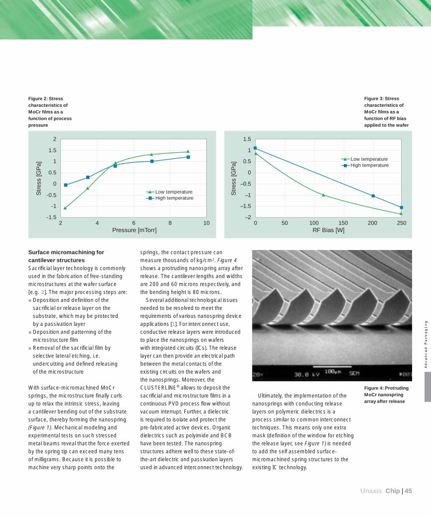
Unaxis Chip | 45
Advanced Packaging
Surface micromachining forcantilever structuresSacrificial layer technology is commonlyused in the fabrication of free-standingmicrostructures at the wafer surface [e.g. 3]. The major processing steps are: Deposition and definition of the
sacrificial or release layer on thesubstrate, which may be protected by a passivation layer
Deposition and patterning of themicrostructure film
Removal of the sacrificial film byselective lateral etching, i.e.undercutting and defined releasing of the microstructure
With surface-micromachined MoCrsprings, the microstructure finally curls up to relax the intrinsic stress, leaving a cantilever bending out of the substratesurface, thereby forming the nanospring (Figure 1). Mechanical modeling andexperimental tests on such stressed metal beams reveal that the force exertedby the spring tip can exceed many tens of milligrams. Because it is possible tomachine very sharp points onto the
springs, the contact pressure canmeasure thousands of kg/cm2. Figure 4shows a protruding nanospring array afterrelease. The cantilever lengths and widthsare 200 and 60 microns respectively, andthe bending height is 80 microns.
Several additional technological issuesneeded to be resolved to meet therequirements of various nanospring deviceapplications [1]. For interconnect use,conductive release layers were introducedto place the nanosprings on wafers with integrated circuits (ICs). The releaselayer can then provide an electrical pathbetween the metal contacts of the existing circuits on the wafers and the nanosprings. Moreover, theCLUSTERLINE® allows to deposit thesacrificial and microstructure films in acontinuous PVD process flow withoutvacuum interrupt. Further, a dielectric is required to isolate and protect the pre-fabricated active devices. Organicdielectrics such as polyimide and BCBhave been tested. The nanospringstructures adhere well to these state-of-the-art dielectric and passivation layersused in advanced interconnect technology.
Ultimately, the implementation of thenanosprings with conducting releaselayers on polymeric dielectrics is aprocess similar to common interconnecttechniques. This means only one extramask (definition of the window for etchingthe release layer, see Figure 1) is neededto add the self assembled surface-micromachined spring structures to theexisting IC technology.
-1.5
-1
-0.5
0
0.5
1
1.5
2
2 4 6 8 10Pressure [mTorr]
Str
ess
[GP
a]
Low temperature High temperature
–2
–1.5
–1
–0.5
0
0.5
1
1.5
0 50 100 150 200RF Bias [W]
Str
ess
[GP
a]
250
Low temperature High temperature
Figure 2: Stresscharacteristics ofMoCr films as afunction of processpressure
Figure 3: Stresscharacteristics ofMoCr films as afunction of RF biasapplied to the wafer
Figure 4: ProtrudingMoCr nanospringarray after release
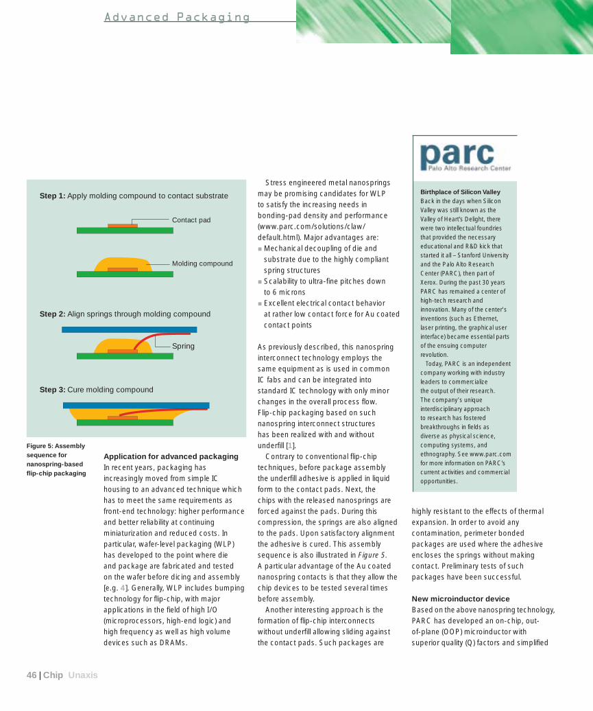
Contact pad
Molding compound
Spring
Step 1: Apply molding compound to contact substrate
Step 2: Align springs through molding compound
Step 3: Cure molding compound
46 | Chip Unaxis
Stress engineered metal nanospringsmay be promising candidates for WLP to satisfy the increasing needs in bonding-pad density and performance(www.parc.com/solutions/claw/default.html). Major advantages are: Mechanical decoupling of die and
substrate due to the highly compliantspring structures
Scalability to ultra-fine pitches down to 6 microns
Excellent electrical contact behavior at rather low contact force for Au coatedcontact points
As previously described, this nanospringinterconnect technology employs thesame equipment as is used in common IC fabs and can be integrated intostandard IC technology with only minorchanges in the overall process flow. Flip-chip packaging based on suchnanospring interconnect structures has been realized with and withoutunderfill [1].
Contrary to conventional flip-chiptechniques, before package assembly the underfill adhesive is applied in liquidform to the contact pads. Next, the chips with the released nanosprings areforced against the pads. During thiscompression, the springs are also alignedto the pads. Upon satisfactory alignmentthe adhesive is cured. This assemblysequence is also illustrated in Figure 5.A particular advantage of the Au coatednanospring contacts is that they allow thechip devices to be tested several timesbefore assembly.
Another interesting approach is theformation of flip-chip interconnectswithout underfill allowing sliding againstthe contact pads. Such packages are
highly resistant to the effects of thermalexpansion. In order to avoid any contamination, perimeter bondedpackages are used where the adhesiveencloses the springs without makingcontact. Preliminary tests of suchpackages have been successful.
New microinductor deviceBased on the above nanospring technology,PARC has developed an on-chip, out-of-plane (OOP) microinductor withsuperior quality (Q) factors and simplified
Birthplace of Silicon ValleyBack in the days when SiliconValley was still known as theValley of Heart’s Delight, therewere two intellectual foundriesthat provided the necessaryeducational and R&D kick thatstarted it all – Stanford Universityand the Palo Alto ResearchCenter (PARC), then part ofXerox. During the past 30 yearsPARC has remained a center ofhigh-tech research andinnovation. Many of the center'sinventions (such as Ethernet,laser printing, the graphical userinterface) became essential partsof the ensuing computerrevolution.
Today, PARC is an independentcompany working with industryleaders to commercialize the output of their research. The company's unique interdisciplinary approach to research has fosteredbreakthroughs in fields as diverse as physical science,computing systems, andethnography. See www.parc.comfor more information on PARC’scurrent activities and commercialopportunities.
Application for advanced packagingIn recent years, packaging hasincreasingly moved from simple IChousing to an advanced technique whichhas to meet the same requirements asfront-end technology: higher performanceand better reliability at continuingminiaturization and reduced costs. Inparticular, wafer-level packaging (WLP)has developed to the point where die and package are fabricated and tested on the wafer before dicing and assembly [e.g. 4]. Generally, WLP includes bumpingtechnology for flip-chip, with majorapplications in the field of high I/O(microprocessors, high-end logic) andhigh frequency as well as high volumedevices such as DRAMs.
Figure 5: Assemblysequence fornanospring-basedflip-chip packaging
Advanced Packaging

manufacturing on a wide range ofsubstrates (www.parc.com/solutions/oopcoil). Figure 6 shows such a microinductor device integrated withactive circuitry. This new coil holds manypotential advantages for applications suchas cell phones, TV tuners, and wirelesslocal networks. It is also suitable for otherradio frequency integrated circuit (RFIC)and microwave applications.
What’s next?The collaboration between PARC andUnaxis Semiconductors has lead tosuccessful results with stressed metalmicrostructures and promises to bringabout even more innovations in the future.In particular, PARC has pioneered highlycompliant nanosprings based on specialMoCr alloys with pitches below 10 µm for the next generation of high densityinterconnects.
The CLUSTERLINE® system, with itssuperior cost of ownership for advanced
Unaxis Chip | 47
Advanced Packaging
packaging applications and its highprocess flexibility and performance, allowsprecise control for optimization of this new stress technology as well asintegration of nanospring devices withstandard interconnect technology.
For more information please contact:[email protected]
References1 D.K. Fork et al., Stress Engineered Metal
Interconnects, 2001International Conference on High DensityInterconnect and Systems Packaging, SantaClara, CA, April 2001, pp. 195 –200
2 D.L. Smith et al., A New Flip-Chip Technology for High-Density Packaging, Proc. 46th Electron.Comp. Tech. Conf., Orlando, FL, May 1996, pp. 1069 –1073
3 C. Linder et al., Review – Surface Micromachining, J. Micromech. Microeng.(IOP UK), Vol. 2, (1992), pp. 122–132
4 IMAPS 2002, Session: Recent Developments in Wafer Level CSPs, 35th Annual Symposiumon Microelectronics, Denver, CO, Sept. 2002
Dave ForkDave Fork is currently aPrincipal Scientist at thePalo Alto Research Center(PARC). He graduatedSumma cum Laude fromthe University of Rochesterin 1987 with degrees inPhysics and ElectricalEngineering and completedhis Ph.D. from StanfordUniversity in AppliedPhysics in 1991. Workingprimarily on thin filmelectronic materials anddevices, his researchactivities include complexoxide epitaxial thin films,laser crystallized displaymaterials, organic electroluminescent devices,semiconductor LEDs and lasers, electronicimaging systems, andmicro-electromechanicalsystems.
Figure 6: Out-of-planemicroinductorsintegrated with activecircuitry
Sputtering targets with excellentproperties are fundamental forthe reliable formation of highquality films. For the MoCr targetof the nanosprings, low oxygenand high purity powders wereblended in a proprietary mixingprocess and then compressed to100% density under vacuum in ahot isostatic press.Working together with both theUnaxis Semiconductors andPARC research teams, theHereaus Materials (previouslyUnaxis Materials USA, Inc.)experts were able to develop andproduce a high-quality target forthe functional MoCr layers. Thetarget was developed specificallyfor this project and perfectlyillustrates how appropriate know-how and flexibility enable entryinto new markets andapplications.

48 | Chip Unaxis
APiA – the Advanced Packaging andInterconnect Alliance – is an association of leading equipment, process technologyand process material companiesrepresenting the foremost authorities onemerging packaging and interconnecttechnologies. The APiA is focused onaccelerating the development andimplementation of commercially viable,comprehensive and risk-free packagingsolutions which address the escalatingmanufacturing and performancechallenges of leading-edge chipmakersworldwide. The founding members of the alliance – August Technology, Casio,Dainippon Screen, Ebara, the Flip ChipDivision of K&S, Ultratech and Unaxis –represent Asia, Europe and the UnitedStates, providing a culturally diverseorganization representing the strengths of each geographical region.
Semicon Europa 2002 in Munich was a perfect opportunity for members as wellas customers to interface and discuss thelatest in advanced packaging technology.
The APiA seminar took place at the ICM Hall and was hosted by Hans Auer,Advanced Packaging General Manager at Unaxis Semiconductors. He gave anoutline of the interesting mixture of market and technology topics to bepresented: “We have invited not onlyspeakers from member companies, but also four guest speakers who will give us an insight into their work”.
Anticipated growth in the market is becoming a reality Guest speaker Doug Fiechts fromTechSearch International is convinceddespite the slow growth in the semiconductor sector for 2001, the future of the flip chip market is bright. He sites the anticipated growth in themarket is finally becoming a reality as aresult of performance and form factordrivers coupled with infrastructuredevelopments. There are more than twodozen wafer bumping companies andmore than 20 companies offering flip chipbonders / mounters for a variety ofapplications. Microvia substrate technologyis maturing and the number of suppliers is increasing. Furthermore, new underfill
material has been developed. Therefore,the demand for gold and solder bumpedwafers is anticipated to grow to 15 millionwafers (200 mm equivalent) by 2005(Figure 1).
Ellery Buchanan – Chairman of theAlliance, and Sr. Vice President ofMarketing & Corporate Development with Ultratech Stepper, Inc. – gave theintroduction to the APiA. He reviewed the goals of the Alliance, its organizationalstructure, the benefits that arise from APiAand how businesses can participate inany of the following ways: As a customer (for process development
and characterization, equipmentdemonstration and procurement, andparticipating in the seminar /educationalprograms),
As a member (Pilot/Demo line participation, taking part in the seminar/educational programs and involvementin the APiA’s various sub-committees) or
As a Standards Committee member.Buchanan sees two major goals for APiA: first, to ensure the availability ofcomprehensive commercial solutions that meet the productivity and processrequirements defined by the market,
Solder bumped FCIP (flip chip in package)and FCOB (flip chip on board)
4000
3500
3000
2500
2000
1500
1000
500
02000 2001 2002 2003 2004 2005
FCOB FCIP
© 2001 TechSearch International, Inc.
APiA Builds Momentum
Figure 1: Expectedgrowth in the flip chipmarket
At Semicon Europa2002, Doug Fiechtsfrom TechSearchInternationalpresents a brightfuture for the flipchip market.
Nicole Lippuner, Marketing Communications
Advanced Packaging
Unaxis Chip | 49
July
September
October
November
December
even
ts even
ts
10th –12th
17th – 19th
22nd – 24th
16th – 18th
18th – 19th
1st – 4th
8th – 11th
5th – 6th
11th – 13th
4th – 6th
IPFA Singaporewww.ieee.org/ ipfa
Semicon West, San Jose, San Franciscohttp://events .semi.org /semiconwest
Semicon Taiwanhttp://events.semi.org /semicontaiwan
Diskcon USAwww.diskcon.com
BACUS Photomask Technologyhttp://spie.org /conferences
ESREF, Europewww.diee.unica.it/ESREF2002
ISTFA, Phoenixwww.asminternational.org/istfa/
CS-MAX, San Josewww.compoundsemiconductor.net /csmax
Semicon Japanhttp://events.semi.org /semiconjapan
For updates please visit www.semiconductors.unaxis.com
Unaxis Insights
and second, to establish an organizedand professional effort to createguidelines and standards which willenable the adoption of advancedpackaging and interconnect solutions.
Overwhelming interest for APiA membershipAlthough the Alliance was only founded in December of last year, it has alreadyachieved much, including: Active committees focused on pilot line
development and implementation Developing a Standards Committee
strategy in conjunction with SEMI and JEDEC
The Commercial Offering Committeeactively working on Alliance members better serving their customers together
The Education Committee having active dialogue with universities
Holding four seminars and a roadshowin Asia
The attendees of the APiA SemiconEuropa seminar were impressed by theinformative presentations and theopportunity to interact with industryleaders. The question and answer periodwas active and engaging.
Buchanan summarized APiA’s impact:“We are overwhelmed by the interest ofcompanies wanting to join APiA asassociate members. Fifteen companieshave joined to date, and numerous otherapplications have been received. This is atestimony to the interest in this emergingand burgeoning market.”
APiA delegation to ChinaThe recent APiA delegation to China had the opportunity to meet the ViceMayor of Shanghai Municipal People’sGovernement, the Honorable YuPengZhou. The delegation, headed by ArtZafiropoulo, Chairman and CEO ofUltratech Stepper, discussed the issuesinvolved in building the semiconductorequipment and materials infrastructure in China.
From left to right: Travis Wang,Entegris; Stephen Strausser,Ebara; Charlie Zhou, Clariant; TomTogasaki, SEZ; Ellery Buchanan,Ultratech, Chairman APiA; JaneZhao-Quan, Berkeley ConsultingGroup; Art Zafiropoulo, Ultratech,leader of the delegation; YuPengZhon, Vice Mayor of Shanghai;Ernst Gloor and Benjamin Loh,Unaxis Semiconductors; TakeshiWakabayashi, Casio; Akira Owatri,Ebara; Clement Lam, HellerIndustries; Wai Mun Lee, EKC

North AmericaUnaxis USA Inc., [email protected] Tel +1 727 577 4999Fax +1 727 577 7035
EuropeUnaxis Balzers AG, [email protected] Tel +423 388 6237 Fax +423 388 6254
ChinaUnaxis (Shanghai) Co., [email protected] Tel +86 21 5057 4646Fax +86 21 5057 4647
SingaporeUnaxis Singapore Pte. [email protected] Tel +65 6890 6288 Fax +65 6890 6290
KoreaUnaxis Korea Ltd., [email protected] Tel +82 31 708 8666Fax +82 31 708 7666
Taiwan Unaxis Taiwan Ltd., Hsin [email protected] Tel +886 3597 7771Fax +886 3598 6363
JapanUnaxis Japan Co. Ltd., [email protected] +81 3 3225 9020Fax +81 3 3225 9043
Other MarketsUnaxis Balzers [email protected] Tel +41 81 784 6237Fax +41 81 784 6254
www.semiconductors.unaxis.com