opuser xp 1.20 suite comprise of schematic editor simulators … catalog/opuser... ·...
TRANSCRIPT

OPUSER XP 1.20 suite comprise of Schematic Editor, Simulators – Mixed Mode Simulator and SPICE based simulator EDSpice, PCB Layout Editor – Create the PCB Layout, Fabrication Manager – generate Manufacturing output files for Photoplotter, NC Drill etc. Thermal Analyzer – check for hotspots on the board, Electromagnetic Analyzer (with Signal Integrity and Field analyzer) – check for electromagnetic effects on the board, 30,000+ Library Components and Library Editor for library component creation. OPUSER XP 1.20 Released. The price-performance leader is now back with a powerful set of new features - 3D Viewers and Editors, VHDL Editor with facility of automatic project creation from VHDL source and Converters (CUPL, JEDEC, XILINX), Model Generators from VHDL for Mixed Mode and EDSpice Simulators with facility of automatic creation of model/ library along with other features. Apart from the major attraction, completely integrated design concept with Automatic Front and Back Annotation.
Schematic; 81 x 81 Cm x 99 sheet max. / project Layout; 81 x 81 Cm x 32 Layer max/ project
Possible to select from 2 version & 3 package Pro version: full support licence NC version: cheaper prices & Non support

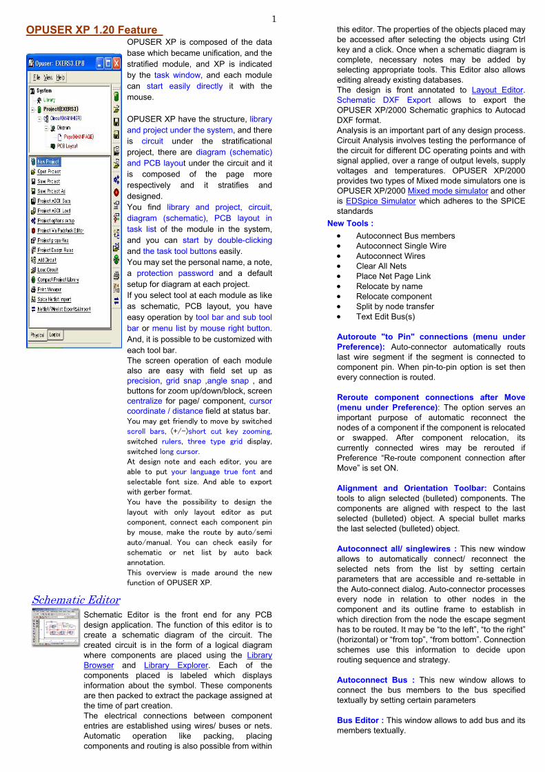
1OPUSER XP 1.20 Feature
OPUSER XP is composed of the data base which became unification, and the stratified module, and XP is indicated by the task window, and each module can start easily directly it with the mouse. OPUSER XP have the structure, library and project under the system, and there is circuit under the stratificational project, there are diagram (schematic) and PCB layout under the circuit and it is composed of the page more respectively and it stratifies and designed. You find library and project, circuit, diagram (schematic), PCB layout in task list of the module in the system, and you can start by double-clicking and the task tool buttons easily. You may set the personal name, a note, a protection password and a default setup for diagram at each project. If you select tool at each module as like as schematic, PCB layout, you have easy operation by tool bar and sub tool bar or menu list by mouse right button. And, it is possible to be customized with each tool bar. The screen operation of each module also are easy with field set up as precision, grid snap ,angle snap , and buttons for zoom up/down/block, screen centralize for page/ component, cursor coordinate / distance field at status bar. You may get friendly to move by switched scroll bars, (+/-)short cut key zooming, switched rulers, three type grid display, switched long cursor. At design note and each editor, you are able to put your language true font and selectable font size. And able to export with gerber format. You have the possibility to design the layout with only layout editor as put component, connect each component pin by mouse, make the route by auto/semi auto/manual. You can check easily for schematic or net list by auto back annotation. This overview is made around the new function of OPUSER XP.
Schematic Editor is the front end for any PCB design application. The function of this editor is to create a schematic diagram of the circuit. The created circuit is in the form of a logical diagram where components are placed using the Library Browser and Library Explorer. Each of the components placed is labeled which displays information about the symbol. These components are then packed to extract the package assigned at the time of part creation. The electrical connections between component entries are established using wires/ buses or nets. Automatic operation like packing, placing components and routing is also possible from within
this editor. The properties of the objects placed may be accessed after selecting the objects using Ctrl key and a click. Once when a schematic diagram is complete, necessary notes may be added by selecting appropriate tools. This Editor also allows editing already existing databases. The design is front annotated to Layout Editor. Schematic DXF Export allows to export the OPUSER XP/2000 Schematic graphics to Autocad DXF format. Analysis is an important part of any design process. Circuit Analysis involves testing the performance of the circuit for different DC operating points and with signal applied, over a range of output levels, supply voltages and temperatures. OPUSER XP/2000 provides two types of Mixed mode simulators one is OPUSER XP/2000 Mixed mode simulator and other is EDSpice Simulator which adheres to the SPICE standards
New Tools : • Autoconnect Bus members • Autoconnect Single Wire • Autoconnect Wires • Clear All Nets • Place Net Page Link • Relocate by name • Relocate component • Split by node transfer • Text Edit Bus(s) Autoroute "to Pin" connections (menu under Preference): Auto-connector automatically routs last wire segment if the segment is connected to component pin. When pin-to-pin option is set then every connection is routed. Reroute component connections after Move (menu under Preference): The option serves an important purpose of automatic reconnect the nodes of a component if the component is relocated or swapped. After component relocation, its currently connected wires may be rerouted if Preference “Re-route component connection after Move” is set ON. Alignment and Orientation Toolbar: Contains tools to align selected (bulleted) components. The components are aligned with respect to the last selected (bulleted) object. A special bullet marks the last selected (bulleted) object. Autoconnect all/ singlewires : This new window allows to automatically connect/ reconnect the selected nets from the list by setting certain parameters that are accessible and re-settable in the Auto-connect dialog. Auto-connector processes every node in relation to other nodes in the component and its outline frame to establish in which direction from the node the escape segment has to be routed. It may be “to the left”, “to the right” (horizontal) or “from top”, “from bottom”. Connection schemes use this information to decide upon routing sequence and strategy. Autoconnect Bus : This new window allows to connect the bus members to the bus specified textually by setting certain parameters Bus Editor : This window allows to add bus and its members textually.
Schematic Editor

2
Simulation is a design analysis, which replaces design symbols with their Simulation models and provides a detailed analysis of their behavior. For Simulating a designed circuit, the model of the real circuit is created taking all factors into consideration, and the appropriate inputs are given. Then the outputs at each level are checked and corrections or modifications are made. Hierarchical simulation has been implemented in OPUSER XP/2000 Mixed Mode Simulator. The simulator now supports simulation of hierarchical databases. In addition to that, two new analysis has been introduced in Mixed mode simulator that assist end users to design the circuit precisely. Monte Carlo analysis is used to calculate component parameter values for a given output at a given instant of time. Sensitivity analysis points out the most sensitive component to a particular parameter such as voltage, current, etc. During simulation all factors are taken into consideration and a model of the real circuit is created and the inputs are given accordingly. Then the outputs at each level are checked and corrections or modifications, if any, are made. There are a number of algorithms used universally to simulate a circuit. The Mixed-Mode Simulator is one of the best tools used. It can simulate analog, digital as well as a combination of analog-digital circuits. It is a de facto that an analog simulator equipped with a logic simulation engine that models the digital parts of a circuit during the Transient Analysis run. The commonly used functions by the simulator are: Bias point calculation, Transient analysis, Parameter sweep analysis, DC Sweep Analysis, AC Sweep Analysis, Monte Carlo Analysis, Sensitivity Analysis, Preprocessing pass.
The EDSpice Simulator is a plug-in extension of the OPUSER Electronics CAD/ CAE System. It provides OPUSER users with the facility to analyze and validate the functionality and behavior of circuits captured in the form of schematic diagrams. The EDSpice Simulator is based on SPICE 3F5 and XSPICE with a number of extensions and improvements. SPICE 3F5 was developed by the University of California and XSPICE was developed by Georgia Tech Research Institute. SPICE is well known in the electronics industry as a general-purpose circuit simulation program for nonlinear dc, nonlinear transient and linear ac analyses. XSPICE extends SPICE3's capabilities to allow simulation of mixed-signal (analog/digital) and mixed-level circuits. EDSpice is a separate product and must not be confused with OPUSER XP/2000's current Mixed Mode Simulator. Apart from simulating circuits captured using the editing functions of the OPUSER XP/2000 Schematic Editor package, experienced SPICE users may simulate circuits generated by other CAD/ CAE packages, capable of producing netlists complying with the Berkeley SPICE2G.6 format. An additional feature allows you to recreate the schematic part of OPUSER XP/2000's circuit projects, by importing files in the above-mentioned standard. SPICE netlist or input files (.CIR) generated by OPUSER XP/2000 (function of EDSpice Simulator interactive module) are fully compatible with the Berkeley standard. This means that circuits
captured in OPUSER XP/2000 may be simulated by any third party SPICE simulator. Layout Editor is used to design the PCB layout of a circuit. The design can be captured either in schematic capture or directly in layout editor. In the former case, the design is front annotated to the layout editor and in the latter case it is back annotated to schematic editor. Also allows beginning layout without a preexisting schematic. In layout the components are placed using Library Browser or Library Explorer. Each of the components placed is labeled which displays information about the package. The component pins are connected using trace or nets. Automatic operations like DRC check, renumbering of components, placing components and routing is also possible from within this editor.The components may be autorouted using Arizona autorouter, which is an integrated module of OPUSER XP/2000. SPECCTRA Translator supports different options like converting OPUSER XP/2000 project (database) to SPECCTRA compatible format, importing results from SPECCTRA Autorouter and Autoplacer etc. MaxRoute Translator allows to convert OPUSER XP/2000 layout project (database) to a form that is acceptable to MaxRoute Autorouter and MaxRoute Autoplacer. Once when a design is complete, necessary notes may be added by selecting appropriate tools. This Editor also allows editing already existing Projects. OPUSER provides two board level analyzers. The Thermal Analyzer is intended to be used for analyzing and identifying potential thermal problems on a Printed Circuit Board. The Electromagnetic Analyzer is used for understanding the distribution of Electric field intensity over a routed PCB. Signal integrity analysis allows you to calculate how substantial the signal gets distorted while it passes through the selected trace.
New Tools • Auto Connect Net • Auto Connect Node Pair • Auto Connect Traces • Clear All Nets • Relocate component • Text Edit Bus(s) lay Autocheck (menu under Auto): This function is now improved and provides various other parameters to check the board for any violation taking into consideration the various design rules set for the board Reroute component connections after Move (menu under Preference): The option serves an important purpose of automatic reconnect the nodes of a component if the component is relocated or swapped. After component relocation, its currently connected wires may be rerouted if Preference “Re-route component connection after Move” is set ON. Alignment and Orientation Toolbar: Contains tools to align selected (bulleted) components. The components are aligned with respect to the last selected (bulleted) object. A special bullet marks the last selected (bulleted) object.
Layout Editor
Mixed Mode Simulator
EDSpice Simulator

3 Check other DR violations : The dialog box presented below allows setting the values for various other design rule parameters for a layout. The parameters defined in this window works in conjunction with the values set in DEFAULT DESIGN RULES window. Once the parameters is set for the design externally using DEFAULT DESIGN RULES window, necessary options shall be set in CHECK OTHER DR VIOLATIONS window and the program will output errors accordingly. DRC Setup : This dialog box allows setting various values for Design Rule Check of the PCB. New Shortcut Keys : Object Distance (Shortcut key SHIFT+M): A new feature to measure the distance between the selected object (as the reference object) and any other object is included in this version. The distance of measurement is displayed in the status bar provided below the editor. This function is made possible with the help of the Shortcut key command, SHIFT+M. After pressing SHIFT+M (message on the status bar prompts to select the object) click on any object. Keeping this object as the reference, move the cursor to any other object on the graphics area. The distance of measurement is displayed in the status bar concurrently, according to the movement of the cursor. Override snap set in Design Rule Check(Press CTRL): In earlier version, snap value may be enabled or disabled by clicking on the icon of snap. However, in this release snap has been improved to suit best the environment. In addition to the snap value set in the layout module, it may also be set in Design Rule Check dialog also. In this case, the snap value set in Design Rule Check dialog has higher priority over the value set in layout editor. A typical example follows. Two snap values can be set in Layout. This is required when certain items require snap value say .0100” whereas certain other items require snap value say .1000”. The snap value that is required for most of the items can be set in Design Rule Check dialog so that the other snap value required only for certain object can be set in layout editor. By default, the user may now work with the value set in Default Design rule. To use the snap value set in Layout Editor, the user may use CTRL key and work with the current settings in Layout Editor. Ctrl+Spacebar: Alternate method to Redraw--> Current. Arizona autorouter is an integrated module of OPUSER XP/2000. It uses its own temporary project and simplified graphics. The Arizona autorouter allows to route the traces of a PCB Layout automatically. The netlists is given as the input to the autorouter. When this router option is selected, all nonorthogonal traces will be removed and accepts only orthogonal traces as prerouted traces. SPECCTRA Translator supports different options like converting OPUSER XP/2000 project (database) to SPECCTRA compatible format, importing results from SPECCTRA Autorouter and Autoplacer etc. MaxRoute Translator allows to
convert OPUSER XP/2000 layout project (database) to a form that is acceptable to MaxRoute Autorouter and MaxRoute Autoplacer. Thermal Analyzer is an application that allows analyzing the effects of temperature parameters in the functioning of the circuit. The thermal effects generated by the board parameters, component parameters, cooling parameters etc. may directly influence the working of the circuit. The analysis can be done with the parameters set to the required values and the analyzer does the analysis taking into consideration the effects caused by these parameters. The Thermal Analyzer contains a full set of functions for setting the different parameters, running the analysis and displaying the result of the analysis using isotherms or color mapping scheme. ED-EMA is a tool to calculate and measure the magnetic radiation of your PCB design. Thus, to help you save money on costly manufacturing steps, until you get an acceptable design and to help you comply with the EMC rules for CE certification and to maintain a proper documentation. Find out about Crosstalks, Improper placement, Shieldings, and more, when your design is still a design. Save your results for your documentation. ED-EMA is a true 32-bit application that runs on all Windows platforms including Windows 3.1X (Win32s DLLs required), Windows `9x ,Windows NT,Wndows 2000 and Windows XP. Special compliment to EMC users - Signal Integrity - is an add-on option available which is used to check the integrity of an electromagnetic signal as it passes through a trace from one pin to another pin. Thus predicting, how a signal deviates from its ideal (or intended) behavior in a real-world setting. The simulation result will be graphically presented using the Diagram Generator. Field Analyzer The Field Analyzer is a tool for studying the electromagnetic fields that are created when power and/or signal traces on the board are energized. The three main out puts of Fabrication manager are Gerber, NC Drill, PCB Assembly Outputs and Bare Board Test Data required for photoplotting. Gerber is the accepted standard format used as input to photoplotters that generate the design data on films. These films are used as masters for manufacturing the PCB, the physical realization of the schematic data. The Gerber output of the layout design is converted to an Artwork file to view in OPUSER. The major tasks done with Fabrication Manager is as follws.
Optional creation of Copper Planes and Copper Pour Areas
Adding dimensions and notes Printing layout documentation drawings
Fabrication Manager
Electromagnetic Analyzer
Arizona autorouter
Thermal Analyzer

4 Extracting NC-drill data to disk files or paper tape
Editing, dimensioning and printing of drill templates
Editing and printing of layer artworks Generation of artwork data files in Gerber ASCII format
Preview of artworks in Gerber ASCII files Generation of disk files containing generic data for Pick & Place machines
Generation of disk files containing bill of materials
The function of the tool Library Browser is to browse library elements (Parts/ Symbols/ Packages/ Padstack) from the available libraries (including Project library) included in the search sequence. The system will search for these components in the library and append to the search list. Apart from component name, various other information may be specified such as symbol name, package name, manufacture etc. to make the search easier. User can use wildcard combination also.the elements in the generated list (search list) may be viewed using the viewer individually and subsequently, output the list to an ASCII file. The alias of the selected part (from the list) may also be obtained.The elements in the generated list (search list) may be viewed using the viewer individually and subsequently, output the list to an ASCII file. The alias of the selected part (from the list) may also be obtained. The list may be cleared and a new search may be initiated. The fields of each component in the list may be enabled according to ones use. Users are allowed to register the type of components to be used in the project. These searched items in the list may be placed on the schematic/ layout by either of the two ways.
Drag and Drop components and Right click on the component(s) in the search
and select Send To Schematic or Layout. For both the above two methods multiple selection is possible as in Windows Explorer. Similarly, the symbol, package and padstack may be searched and further operation may be carried out. For easier operation on the libraries, OPUSER XP/2000 provides Library Explorer in which the user can see the available libraries specified in the path. All library components in the specified are displayed irrespective of the libraries added in the search sequence. Library Editor is used to add new or edit existing components to the list already supplied with OPUSER XP/2000. Waveform Viewer may be used to generate results in the form of diagram for Mixed Mode Simulator, EDSpice Simulator and Signal Integrity Simulation. This diagram represents the data generated by simulators to present the simulation results in a graphical format. The graphical format may be displayed on the screen, output to a printer or save it as a part to place it on your actual schematic drawing. The functionality of Diagram Generator has been enhanced to help end users to examine the output diagrams of different analysis in a better way. In the new Waveform Viewer (the enhanced version of Diagram Generator), there is no limit to
the number of variables that may be loaded. At the same time it is capable of handling any number of samples and hence the simulation time has no limit. he diagrams may be saved to or loaded from a project. Several diagrams can be tiled together to view on a single screen. Tools have been made available to allow users to change the presentation style of the diagram with ease
OPUSER XP 3-Dimensional View OPUSER XP 1.20 has been packed with the most exciting and comprehensive step towards the design of electronic circuit with the concept of three-dimension (3D). Designed electronic circuits (PCB) are usually housed inside cabinets or any intricate structures where spacing between different boards placed has to be dealt with prudently. Working in 3D environment facilitates optical design check. It provides an in-depth analysis of the board density and a realistic view of a designed PCB. The concept of 3D has been incorporated into Layout Editor and Library Editor. Layout Editor consists of 3D Board Viewer and 3D Trace Viewer. Library Editor allows editing and creating of 3D library packages and cabinets. Tools have been provided to assist the user view the board and package from various directions and from different angles. In Layout Editor 3D Board Viewer can be invoked from menu Tools ->3D Board Viewer. 3D Board Viewer gives a real life view of the designed board in various perspectives and directions. It gives idea on how the components are located, whether there is risk of friction between components due to their height and shape, the side on which components are placed, etc. This helps to take any design changes if required. In Layout Editor 3D Trace Viewer can be invoked from menu Tools ->3D Trace Viewer. 3D Trace viewer helps to visualize all the physical connections on board. Traces, vias, buried vias, and copper pour elements can be easily visualized. It helps to examine in detail the path taken by traces of each net .It makes the traces present in internal layers (A to Z) visible as shown.
3D in Library Editor In Library Editor, 3D have been bundled with Package Creation. Also a new concept of Board Cabinet has been introduced. In Package Editor, apart from 3D View Control dialog, a number of function and option tools has been provided to assist the user in editing and orientating the package. A package created in the usual (2D) manner can be converted into 3D using these tools. One can enter the 3D mode from the menu Edit/ 3D Viewer. Package Viewer helps to view the package in 3D. To begin with, when you open Package Editor in 3D Edit mode, you see a small rectangular box with a round pad on it. This is the same default pad, which appears when a new
Library Browser
3D Board Viewer
3D Trace Viewer
Package Editor
Waveform Viewer

5package is opened in Package Editor. In other words, whatever is present on the workspace in normal Package Editor gets depicted in 3D mode. The spacing and positions of boards in cabinets or any intricate mechanical structure may be adjusted using Board Cabinet Editor present in Library Editor.
OPUSER XP 1.20 - VHDL This version of OPUSER XP 1.20 helps to describe the behavior of digital systems with the help of VHDL. Some main features of OPUSER XP 1.20 VHDL Editor are : 1. It compiles the source file and generates wirelist
(*.wrs) output file. 2. The output file (*.wrs) may be imported directly
into OPUSERXP 3. Generates simulatable models in Mixed Mode &
EDSpice Model Generators. 4. Converts the (*.wrs) file to Xilinx, CUPL and
JEDEC formats. VHDL Editor working is very much similar to any normal programming editor. All keywords present in the source are highlighted in Blue. On compiling the error messages will displayed at the output window below. On double clicking the error the corresponding line in the editor window will get highlighted in Red. This helps in faster debugging of source file. Compilation stops at first occurrence of error and output get displayed in output window. Successful compilation of the .vhdl file generates the .wrs file.
OPUSER XP 1.20 - Model Generators The model generators allow converting VHDL source files to models for simulation purposes. Since OPUSER XP supports two forms of simulation – Mixed Mode and EDSpice, two model generators have been included – MM Simulation Model Generator and EDSpice Simulation Model Generator.
Model Generator for Mixed Mode Simulator This tool converts a vhdl source file to a simulatable component in OPUSER XP. This also serves the purpose of making simulation much faster. Since VHDL can be used to create digital models, digital simulation primitives can be created using MM Simulation Model Generator. Earlier, the only way of creating simulation primitives was to model the behaviour of the particular component using Visual C++. Knowledge of programming is naturally not expected of electronic engineers and the need for developing a tool arose which could make creation of models easier. This tool converts a vhdl source file to a simulatable component in EDSpice, the SPICE based simulator of OPUSER XP. This also serves the purpose of making simulation much faster. Since VHDL can only be used to create digital models, only digital simulation models can be created using EDSpice Simulation Model Generator. Note: EDComX and EDPrimX are tools which can be used for creating both analog and digital models,
however it assumes programming knowledge and the user has to build his own simulation primitive dll.
Other New Features of OPUSER XP 1.20 Export/ Import/ and Conversion Utilities
Four new Export and Two Import facilities have been included with this release.
EXPORT formats : OPUSER Schematic Netlist, Xilinx Netlist, CUPL Netlist, JEDEC Netlist.
IMPORT formats : OPUSER Schematic Netlist, VHDL. Also three converters have been included.
OPUSER Schematic Netlist to CUPL Netlist: Converts an OPUSER Schematic netlist created by VHDL compiler to CUPL netlist. OPUSER Schematic netlist to XILINX Netlist:Converts an OPUSER Schematic netlist created by VHDL compiler to XILINX netlist. CUPL netlist to JEDEC netlist: Converts CUPL netlist to JEDEC netlist.
Locking of Dockable Toolbars The new version OPUSER XP 1.20 provides a unique feature to lock the dockable toolbars anywhere within the window. Select the menu Preferences -> Lock Toolbar or use shortcut key (CTRL+H) to lock / unlock the toolbars at that particular position.
Inserting Sizes in Options (Text, Snap, Precision etc)
OPUSER XP Options in the Task Window is for implementing the default settings for the project or changing the current settings and implementing it. The options available include:- General, Files, Colors & Layer Names, Formats, Packaging preferences, Component Label Scheme etc. The new option 'Sizes' is added to it. This option allows to set the default sizes of General Schematic and Layout categories.
General: The Angle Snap and Pick Area sizes may be set here. These changes affect all modules of OPUSER.
Schematic: The schematic objects such as Text Size, Grid Size, Symbol line width, Snap, Precision can be fixed or set here.
Layout: The Layout objects such as Trace/Package Line Width, Air Gap, Pad Size etc can be set here.
Transfer Function Analysis New Transfer Function Analysis is added to Mixed Mode Simulator. Transfer function analysis can be activated by checking the check box under Transient analysis. The generated waveform can be viewed in waveform viewer. The Transfer Function defines the relationship between the inputs and its outputs.
Save all Waveforms (both project and disk file) is added in Diagram Generator
Save All option in Diagram Generator allows to save multiple waveforms simultaneously to the Job folder. The waveforms are identified by default names which include the date and time of creation. Save All to Project allows multiple waveforms to be saved to the current project. The waveforms are identified by default names which include the date and time of creation.
Icons Transparent
Icons in all module are made Transparent
Board Cabinet Editor

6 Creating and Loading Strategies for Semi Autorouting
In Schematic Editor while using Tools->Wires->Route Wire->Autoconnect Wires, it is possible to define a routing strategy including routing schemes, autoconnect rules and routing options like Font Name, Font Size, Minimal Pin Size etc. and can be saved as a Schematic Strategy File (*.SSF) within the Lib folder. These saved strategies can be further loaded in a project for routing.
Copying Component Values. (Option Tool)
This Applies to Schematic Editor and Layout Editor. Tools -> Components -> Repeat Components -> Copy Component Value This option allows to copy the value of the component while replicating the component. Tools->Block Edit->Copy Block-> Copy Component Value This option allows to copy a block of components along with their assigned values. Tools->Block Edit->Load Block-> Copy Component Value This option can be used to load a block of components along with their assigned values.
Component Name ON/OFF for entire board.
This applies to Layout Editor. Multiple component names can be switched On/Off at a time using the option tools in Tools->Components->On/Off Component Name. On Selecting 'On All Component Names' all component names on the board are displayed. On Selecting 'Off All Component Names' all component names on the board are switched off.
Identification of Selected Pin in Layout Through Property Window.
On selecting the function tool Component Property ( Tools-> components -> Component Property) and clicking on a component pin ,the component property window with the selected pin gets highlighted in the Property Window.
Tool Magazine Size Increased from 32 to 500 in Fabrication Manager Setup.
The tool magazine size has increased from 32 to 500 in Fabrication Setup. The older NC Drill machines has a limit for its magazine size. Now the latest NC Drill machine over ride this. So we have increased the limit to 500 tools.
Layout DXF Export The graphical interface of Layout DXF Export has been changed to make it more user friendly. It also provides facility to export 3D information of the board and its contents.
Remembering T-Connection ON/OFF This applies to Schematic Editor and Layout Editor.
Remembers the last set T-Connection status even after restarting OPUSER XP.
Record Simulation Output in Oscillograph as PWL file:
The output values obtained during simulation in oscillograph can be recorded and saved in PWL file. This file can be accessed from Electromagnetic Analyzer while performing Signal Integrity Analysis on a Driver Node.
Merging of PWR/GND Nets While Copying (Option Tool)
Applies to Schematic Editor and Layout Editor New Option tool for Merging PWR/GND Nets while copying. Tools ->Block Edit -> Copy Block -> Merge Pwr/Gnd Nets.(F4)
General features :- Conversion manager is used for the Library Conversion, Database Conversion and EED III Conversion
Waveform Viewer may be used to generate results in the form of diagram for Mixed Mode Simulator, EDSpice Simulator and Signal Integrity Simulation.
Subcircuit Adapter allows existing SPICE subcircuits to be converted into an EDSpice format
The Model Parameter Editor eases the management and creation of model libraries.
List Generator is a utility that allows generating a list containing requisite details of OPUSER XP/2000 component library and Project.
Import Wire lists The OPUSER XP/2000 Wirelist Import utility allows to import wirelist of EED3 and OrCad PCB II formats to OPUSER XP/2000 format.
SPICE Net list Import This utility allows to import both circuit (.cir) and subcircuit (.sbc) files to OPUSER XP/2000.
Export OPUSER XP/2000/EED III Wirelist allows exporting wirelist (netlist) from OPUSER XP/2000 to EED III format.
Export Scicards Netlist allows exporting and saving wirelist (netlist) from OPUSER XP/2000 to Scicard format.
Export OrCAD PCB II Wirelist allows exporting and saving wirelist (netlist) from OPUSER XP/2000 to ORCAD PCB II Wirelist.
Schematic DXF Export is an application that allows to export the OPUSER XP/2000 Schematic graphics to AutoCAD DXF format.
Layout DXF Export is an application that allows to export the OPUSER XP/2000 layout graphics to AutoCAD DXF format.
PC OS; Windows 98,Me,XP,NT,2000
Each trademark are the products of each companies. Specifications subject to change without notice.
AVI PRECISION ENGINEERING PTE LTD1, KALLANG SECTOR #04-03, SINGAPORE 349276. TEL: 65 67483866 FAX: 65 67484810Email: [email protected] Website: http://www.avipre.comCompany Reg No: 199300584 M Skype: avipre