orcad pcb editor166 - ema design automationeducation.ema-eda.com/itrain/pcb_editor_166/lesson... ·...
TRANSCRIPT

6
December, 2012 OrCAD PCB Editor - Version 16.6 6-1
Lesson 6: Importing Logic Information into OrCAD and Allegro PCB Editor
NoteThe labs in this lesson demonstrate how to bring logical data from the schematic capture environment. In the logic import/export process from within the OrCAD and Allegro PCB Editor the Import Logic and Export Logic dialog forms denote the logic type as Design Entry CIS (Capture). The Design Entry CIS (alias DE CIS) encompasses the OrCAD Capture, OrCAD Capture CIS, and Allegro Design Entry CIS products.
Learning Objectives
In this lesson you will do the following:
• Working with logic information from a schematic tool, you will understand the key setup choices to be made when importing logic information into the OrCAD and Allegro PCB Editor layout environment
• The logic information can come from any one of these Design Entry schematic environments
– OrCAD Capture
– OrCAD Capture CIS
– Allegro Design Entry CIS (alias DE CIS)
In this section you will learn about Logic Import, which is the process of importing logic from your schematic capture tool into the OrCAD and Allegro PCB Editor database. You will learn how to import from the design entry schematic environment into the OrCAD and Allegro PCB Editor.
201
Importing Logic Information into OrCAD and Allegro PCB Editor Lesson 6
6-2 OrCAD PCB Editor - Version 16.6 December, 2012
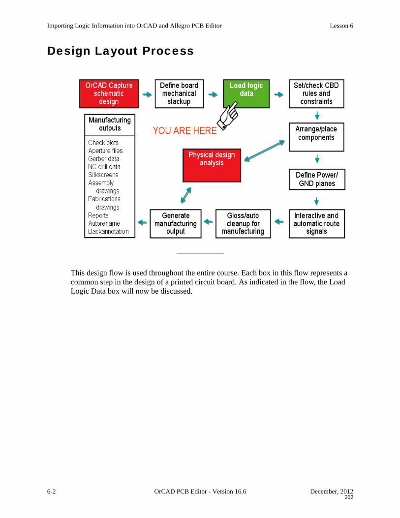
Design Layout Process
This design flow is used throughout the entire course. Each box in this flow represents a common step in the design of a printed circuit board. As indicated in the flow, the Load Logic Data box will now be discussed.
202

December, 2012 OrCAD PCB Editor - Version 16.6 6-3
Lesson 6 Importing Logic Information into OrCAD and Allegro PCB Editor
Integrating Logic Design with Physical Layout
Design Entry CIS (DE CIS) Front End
DE CIS: It is not required that the schematic reside in the same directory as the OrCAD and Allegro PCB Editor design. However, it is recommended that the two be kept together. The minimum values required on a DE CIS schematic library part are Value, Class, and Footprint (package symbol).
Annotate: The Annotate program converts the logic devices into physical packages, assigning a reference designator and physical pin numbers to each symbol in the schematic.
OrCAD and Allegro PCB Editor Netlister: The OrCAD and Allegro PCB Editor Netlister creates the transfer files used by OrCAD and Allegro PCB Editor. By default, these files are created in a directory named allegro.
OrCAD and Allegro PCB Editor
Import Logic: After this step has been completed, the design contains all of the connection information.
203

Importing Logic Information into OrCAD and Allegro PCB Editor Lesson 6
6-4 OrCAD PCB Editor - Version 16.6 December, 2012
OrCAD and Allegro PCB Editor: Used for component placement and routing; allows for pin and gate swaps for optimum routing results; generates manufacturing output.
Export Logic: This program generates backannotation files that the DE CIS tools use to update the schematic.
DE CIS Interface with OrCAD and Allegro PCB Editor
The OrCAD and Allegro PCB Editor Netlister (PXLlite) reads the DE CIS database and creates the same format pst files as the DE HDL Packager XL routine. Therefore, the same program (netrev) can be used by OrCAD and Allegro PCB Editor to read in either a DE CIS schematic or a DE HDL schematic.
For Backannotation, the same OrCAD and Allegro PCB Editor program (genfeed) is used to create the OrCAD and Allegro PCB Editor output files. These files are then read by DE CIS and used to update the schematic to reflect any changes made to the design by OrCAD and Allegro PCB Editor (pin and gate swapping, reference designator changing and so on).
204

December, 2012 OrCAD PCB Editor - Version 16.6 6-5
Lesson 6 Importing Logic Information into OrCAD and Allegro PCB Editor
When you develop the DE CIS schematic libraries, the minimum value information is Class, Value, and Footprint (OrCAD and Allegro PCB Editor Package Symbol).
Transfer Files (pst*.dat) - DE CIS to OrCAD and Allegro PCB Editor
You use the transfer (pst) files generated by the DE CIS Create Netlist command to transfer information from the schematic to a OrCAD and Allegro PCB Editor design. These files are:
File Description
pstxprt.dat This is a parts list file. It lists each physical package (created by the packager) in the schematic, along with its reference designator and device type. For packages comprised of multiple logic gates, this file identifies which gate was placed in which section of the physical package.
This file may also contain some properties attached to parts in the schematic, such as ROOM=’IF’, VALUE=’4.7K’.
205
Importing Logic Information into OrCAD and Allegro PCB Editor Lesson 6
6-6 OrCAD PCB Editor - Version 16.6 December, 2012
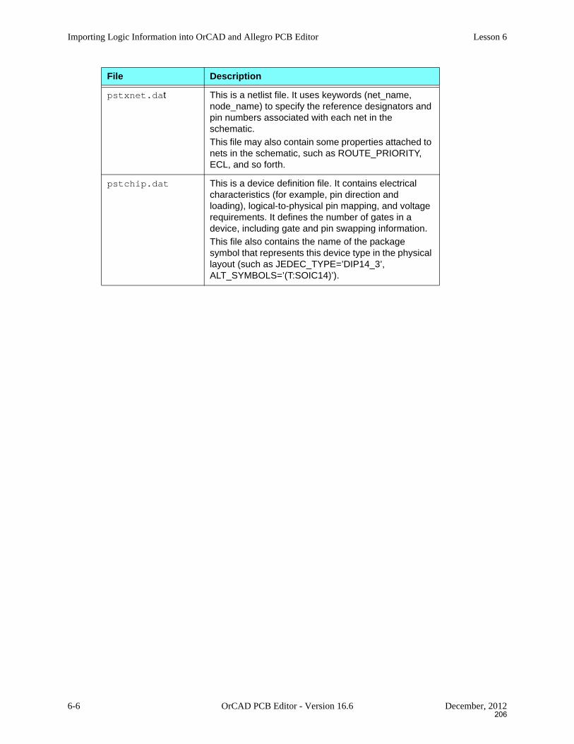
pstxnet.dat This is a netlist file. It uses keywords (net_name, node_name) to specify the reference designators and pin numbers associated with each net in the schematic.
This file may also contain some properties attached to nets in the schematic, such as ROUTE_PRIORITY, ECL, and so forth.
pstchip.dat This is a device definition file. It contains electrical characteristics (for example, pin direction and loading), logical-to-physical pin mapping, and voltage requirements. It defines the number of gates in a device, including gate and pin swapping information.
This file also contains the name of the package symbol that represents this device type in the physical layout (such as JEDEC_TYPE=’DIP14_3’, ALT_SYMBOLS=’(T:SOIC14)’).
File Description
206

December, 2012 OrCAD PCB Editor - Version 16.6 6-7
Lesson 6 Importing Logic Information into OrCAD and Allegro PCB Editor
DE CIS - OrCAD and Allegro PCB Editor Logic Import
After you have annotated your schematics, you must use the OrCAD and Allegro PCB Editor Netlister to create the input files for OrCAD and Allegro PCB Editor. Use the Tools - Create Netlist option from the Project menu in DE CIS or the PCB Editor tab to create the three pst files. These are the same three files (pstchip.dat, pstxnet.dat, pstxprt.dat) created and used in the DE HDL-to-Allegro PCB Editor transfer process.
At the same time you are creating the OrCAD and Allegro PCB Editor interface files, you can also “push” these files into OrCAD and Allegro PCB Editor by using the Create or Update PCB Editor Board (netrev) option. This option will run the OrCAD and Allegro PCB Editor netrev program that will read the interface files and create a new OrCAD and Allegro PCB Editor design or update an existing one.
If you do not want to run the netrev program from the OrCAD and Allegro PCB Editor Netlister inside DE CIS, you can import the interface files from within OrCAD and Allegro PCB Editor. Use the File - Import - Logic command from the top menu in OrCAD and Allegro PCB Editor and choose the DE CIS option. Use the Import Directory field to point to the directory containing the three interface files created by the DE CIS -Allegro PCB Editor Netlister program.
207

Importing Logic Information into OrCAD and Allegro PCB Editor Lesson 6
6-8 OrCAD PCB Editor - Version 16.6 December, 2012
Properties are passed back and forth between these two tools. You define which property names are allowed to pass. They are controlled by listing them in the allegro.cfg file located at <cdsroot>\tools\capture.
Engineering Changes—Placement
With an ongoing design, schematic changes are incorporated (ECO) with the netrev process, which brings in the transfer files from the edited schematics. If the OrCAD and Allegro PCB Editor design has not been placed or routed, the new transfer files simply replace the original OrCAD and Allegro PCB Editor database. If placement has already occurred, you have several options on how the netrev process should proceed.
Place Changed Component: Determines how placed parts are treated in the ECO process. When a part in an edited schematic has a reference designator that matches a placed part in the board layout, parts are compared to determine if there are any changes. If the part has not changed, it maintains its location in the board layout. If the part has changed, you can select one of the following options:
Always replaces the old part in the board layout with the changed part from the edited schematic, regardless of the type, value, or package symbol change (at the same x/y location and rotation as the old part).
208
December, 2012 OrCAD PCB Editor - Version 16.6 6-9
Lesson 6 Importing Logic Information into OrCAD and Allegro PCB Editor
If Same Symbol replaces the old part in the board layout with the changed part from the edited schematic if the package symbol has not changed (type/value change, but same package symbol). If the package symbol has changed, the old part is removed from the layout, and the changed part is added to the board layout database as an unplaced part.
Never removes the old part from the layout and adds the changed part to the board layout database as an unplaced part.
Engineering Changes—Routing
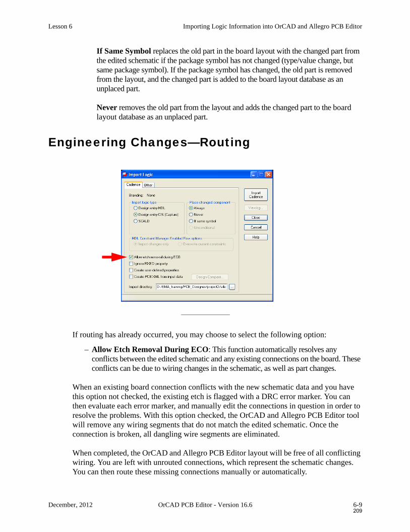
If routing has already occurred, you may choose to select the following option:
– Allow Etch Removal During ECO: This function automatically resolves any conflicts between the edited schematic and any existing connections on the board. These conflicts can be due to wiring changes in the schematic, as well as part changes.
When an existing board connection conflicts with the new schematic data and you have this option not checked, the existing etch is flagged with a DRC error marker. You can then evaluate each error marker, and manually edit the connections in question in order to resolve the problems. With this option checked, the OrCAD and Allegro PCB Editor tool will remove any wiring segments that do not match the edited schematic. Once the connection is broken, all dangling wire segments are eliminated.
When completed, the OrCAD and Allegro PCB Editor layout will be free of all conflicting wiring. You are left with unrouted connections, which represent the schematic changes. You can then route these missing connections manually or automatically.
209

Importing Logic Information into OrCAD and Allegro PCB Editor Lesson 6
6-10 OrCAD PCB Editor - Version 16.6 December, 2012
All part and connectivity changes made to the OrCAD and Allegro PCB Editor layout during the ECO process are documented in a report (eco.txt).
Other options you can use are:
– Ignore FIXED property - If elements in a design have a FIXED property, the new netlist changes will rip up etch or replace components, ignoring that property.
– Create user-defined properties - Allows new properties added in the schematic to be created while logic is being read in.
– Create PCB XML from input data - outputs an XML file that can be read into the PCBCompare tool.
Schematic-Driven Layout (Reference)
It is possible to use the schematic to communicate your physical layout requirements. You can use properties attached to nets and parts in the schematic to affect component placement and signal routing.
Component Definition Properties are usually contained in the chips.prt or PPT files. These properties carry information about the type of physical package required (such as JEDEC_TYPE, ALT_SYMBOLS, PINCOUNT). You can also assign these properties to parts right in the schematic (to specify physical part requirements for the Packager). Schematic values for these properties will override values found in library files.
210

December, 2012 OrCAD PCB Editor - Version 16.6 6-11
Lesson 6 Importing Logic Information into OrCAD and Allegro PCB Editor
Use Comp_Name or Comp_Name_Suffix properties to control type names for new physical parts. These new physical parts (types) are shown in the pstxprt.dat and pstchip.dat files.
Component Instance Properties are properties related to the actual layout process (for example, ROOM, TERMINATOR_PACK, NO_PIN_ESCAPE, NO_MOVE, FIX_ALL, COMPONENT_WEIGHT). These properties appear in the pstxprt.dat file for passage to the OrCAD and Allegro PCB Editor tool. Use the COMP_INST_PROP directive (pxl.cmd file) to specify component instance properties that are included in the pstxprt.dat file.
Schematic Instance Properties control the packaging of functions (gates).
Pin Instance Properties address signal routing requirements.
Net Properties control signal routing and analysis (such as line sizes and clearances, layer restrictions, high speed, priority, length requirements and crosstalk thresholds). These properties appear in the pstxnet.dat file for passage to the OrCAD and Allegro PCB Editor tool.
211
Importing Logic Information into OrCAD and Allegro PCB Editor Lesson 6
6-12 OrCAD PCB Editor - Version 16.6 December, 2012
Labs
• Lab 6-1: DE CIS to OrCAD and Allegro PCB Editor
– Open the master.brd design
– Setup the logic import from DE CIS in the project2/allegro directory
– Import logic and save the new .brd design containing both the physical and netlist information
• Netlist from DE CIDS to OrCAD and Allegro PCB Editor (Optional)
– Open OrCAD Capture
– Create the netlist from the release.dsn design
– Save the design in the OrCAD or Allegro PCB Editor
The following labs will allow you to familiarize yourself with the process required to import a DE CIS schematic into OrCAD and Allegro PCB Editor.
The first lab is the preferred for the class. The second lab is an optional lab to test out the creation of the netlist in OrCAD Capture and automatically import the logic into the OrCAD or Allegro PCB Editor.
212

December, 2012 OrCAD PCB Editor - Version 16.6 6-13
Lesson 6 Importing Logic Information into OrCAD and Allegro PCB Editor
Lab 6-1: DE CIS to OrCAD and Allegro PCB Editor
Objective: Read the physical and netlist information from an DE CIS schematic into an OrCAD and Allegro PCB Editor design file and create a netlist report from the board file.
ImportantLab Directory Instructions: The labs refer to the course installation directory (where you uncompressed the database file) as the <course_inst_dir> directory. Whenever you see a file path in the lab instructions, you must replace the <course_inst_dir> directory with the name of your chosen directory.
Importing the DE CIS File
1. If the OrCAD and Allegro PCB Editor is not currently running, start the OrCAD PCB Editor tool by choose Start - All Programs - Cadence - Release 16.6 - PCB Editor.
The Cadence Product Choices window may appear.
2. If the Product Choices window appears, select OrCAD PCB Designer Professional, and click OK.
3. Open the master.brd design (if is not already open) from within the project2 directory, as shown:
NoteIf you did not complete the lab titled Creating a Master Design File, which saved the board file master.brd into this directory, then use the cds_master.brd file that is provided.
4. Choose File - Import - Logic.
<course inst dir>
PCB_Designer/
project2/play/ solutions/
master.brd
213

Importing Logic Information into OrCAD and Allegro PCB Editor Lesson 6
6-14 OrCAD PCB Editor - Version 16.6 December, 2012
The Import Logic dialog box appears.
5. In the Logic Type section, click Design entry CIS (Capture).
6. In the Import directory field, navigate to the project2/allegro directory (previously generated netlist is located in this directory).
Your Import Logic dialog box should look similar to this:
7. Click Import Cadence.
The DE CIS schematic is checked and imported. If there are errors or warnings, the netrev.lst file automatically displays in a report window when the importing is done. If netrev.lst does not appear, select File - Viewlog from the OrCAD or Allegro PCB Editor main menu to open this file.
8. Close the log file window.
NoteIf you receive a message that the PACKAGER files could not be found, this is because the Import directory field is not pointing directly to the directory containing the netlist files.
9. Select Tools - Quick Reports and select the Bill of Materials Report.
The report shows which components are currently in the database. This will verify your success with loading the netlist into OrCAD and Allegro PCB Editor.
214
December, 2012 OrCAD PCB Editor - Version 16.6 6-15
Lesson 6 Importing Logic Information into OrCAD and Allegro PCB Editor
10. Click the X icon to close the report.
11. Select Display - Status to open the Status window.
The status indicators for Unplaced Symbols and Unrouted Nets should both be red, with 82 out of 82 unplaced symbols, and 181 out of 181 unrouted nets.
12. Select OK to close the Status window.
13. Choose File - Save As.
A file browser window opens.
14. In the Save in field, browse to the project2\allegro directory.
Remember, the Change Directory option has to be enabled to change the working directory.
15. In the File Name field, enter:
unplaced
16. Click Save to save the unplaced.brd file in the project2\allegro directory.
The DE CIS schematic data has been combined with the master design file (mechanical template) to create a new OrCAD and Allegro PCB Editor design file called unplaced.brd. Use this design file to proceed to the next layout phase.
17. At this point you can either exit from the OrCAD and Allegro PCB Editor program by selecting File - Exit, or you can leave this design open, ready to begin lab exercises for the next lesson.
NoteWhen you exit from the OrCAD and Allegro PCB Editor program, files are saved that record your current working directory settings as well as configuration settings and the last file you were working on. If you exit from OrCAD and Allegro PCB Editor at this point in the lab, when you restart OrCAD and Allegro PCB Editor it will automatically open the unplaced.brd file in the <course inst dir>/PCB_Designer/project2/allegro directory. This is what you want for the next lab.
End of LabSTOPSTOP
215

Importing Logic Information into OrCAD and Allegro PCB Editor Lesson 6
6-16 OrCAD PCB Editor - Version 16.6 December, 2012
Lab 6-2: Netlist from DE CIS to OrCAD and Allegro PCB Editor (Optional)
Objective: Netlist information from a DE CIS schematic to an OrCAD and Allegro PCB Editor design file and create a netlist report from the board file.
ImportantLab Directory Instructions: The labs refer to the course installation directory (where you uncompressed the database file) as the <course_inst_dir> directory. Whenever you see a file path in the lab instructions, you must replace the <course_inst_dir> directory with the name of your chosen directory.
Netlisting from DE CIS
1. Make sure that the OrCAD or Allegro PCB Editor is closed.
2. Start the OrCAD Capture tool by choosing Start - All Programs - Cadence - Release 16.6 - OrCAD Capture.
3. Open the release.opj project from within the project2 directory, as shown:
4. Select the release.dsn in the Project Manager window.
5. Choose Tools - Create Netlist.
The Create Netlist form appears.
6. Select the PCB Editor tab.
7. Enable the Create PCB Editor Netlist option.
<course inst dir>
PCB_Designer/
project2/play/ solutions/
release.opj
216

December, 2012 OrCAD PCB Editor - Version 16.6 6-17
Lesson 6 Importing Logic Information into OrCAD and Allegro PCB Editor
8. Make sure that the Netlist Files Directory is pointing to the allegro directory in the project2 directory.
9. Enable the Create or Update PCB Editor Board (Netrev) option.
10. In the Options section, browse the Input Board File selection to either the master.brd file you had created earlier or the cds_master.brd file (both should be located in the project2 directory).
11. The Output Board File should be pointing to a release.brd to be located in the allegro directory.
12. Enable the Open Board in OrCAD PCB Editor option.
Your Import Logic dialog box should look similar to this:
13. Click OK.
The DE CIS schematic is checked and the netlist is created. If there are errors or warnings, the netrev.lst file located in the allegro directory will define the errors.
If an “Unable to open D:\apps\Cadence\Release 16.6\tools\capture\allegro.cfg for reading. Please correct the above errors to proceed.” message appears then click on the Setup button to the left of Create PCB Editor Netlist and browse to the <cds install dir>\tools\capture\allegro.cfg file. Then click on the OK button again at the bottom to create the netlist.
217

Importing Logic Information into OrCAD and Allegro PCB Editor Lesson 6
6-18 OrCAD PCB Editor - Version 16.6 December, 2012
14. When the Cadence Product Choices window appears, select ORCAD PCB Designer Professional.
15. Close the OrCAD Capture tool.
16. In the OrCAD and Allegro PCB Editor, select Place - Manually and notice that your reference designators appear in the Components by refdes window.
17. Select OK to close the Placement window.
18. Choose File - Save As.
A file browser window opens.
19. In the Save in field, browse to the project2\allegro directory.
Remember, the Change Directory option has to be enabled to change the working directory.
20. In the File Name field, enter:
unplaced
21. Click Save to save the unplaced.brd file in the project2/allegro directory.
The DE CIS schematic data has been combined with the master design file (mechanical template) to create a new OrCAD and Allegro PCB Editor design file called unplaced.brd. Use this design file to proceed to the next layout phase.
22. At this point you can either exit from the OrCAD and Allegro PCB Editor program by selecting File - Exit, or you can leave this design open, ready to begin lab exercises for the next lesson.
NoteWhen you exit from the OrCAD and Allegro PCB Editor program, files are saved that record your current working directory settings as well as configuration settings and the last file you were working on. If you exit from OrCAD and Allegro PCB Editor at this point in the lab, when you restart OrCAD and Allegro PCB Editor it will automatically open the unplaced.brd file in the <course inst dir>/PCB_Designer/project2/allegro directory. This is what you want for the next lab.
End of LabSTOPSTOP
218