ordering information · pdf file8 device pin-out diagram ... 9 package mechanical drawings ......
TRANSCRIPT
High Definition Audio Decoder DSP Family with Dual 32-bit Engine Technology
CS4970x4 Data Sheet
Up to 12 Channels of 32-bit Serial Audio Input Customer Software Security Keys 16 Ch x 32-bit PCM Out with Dual 192 kHz S/PDIF Tx
Two SPI™/I2C™ ports Large On-chip X, Y, and Program RAM & ROM SDRAM and Serial Flash Memory Support
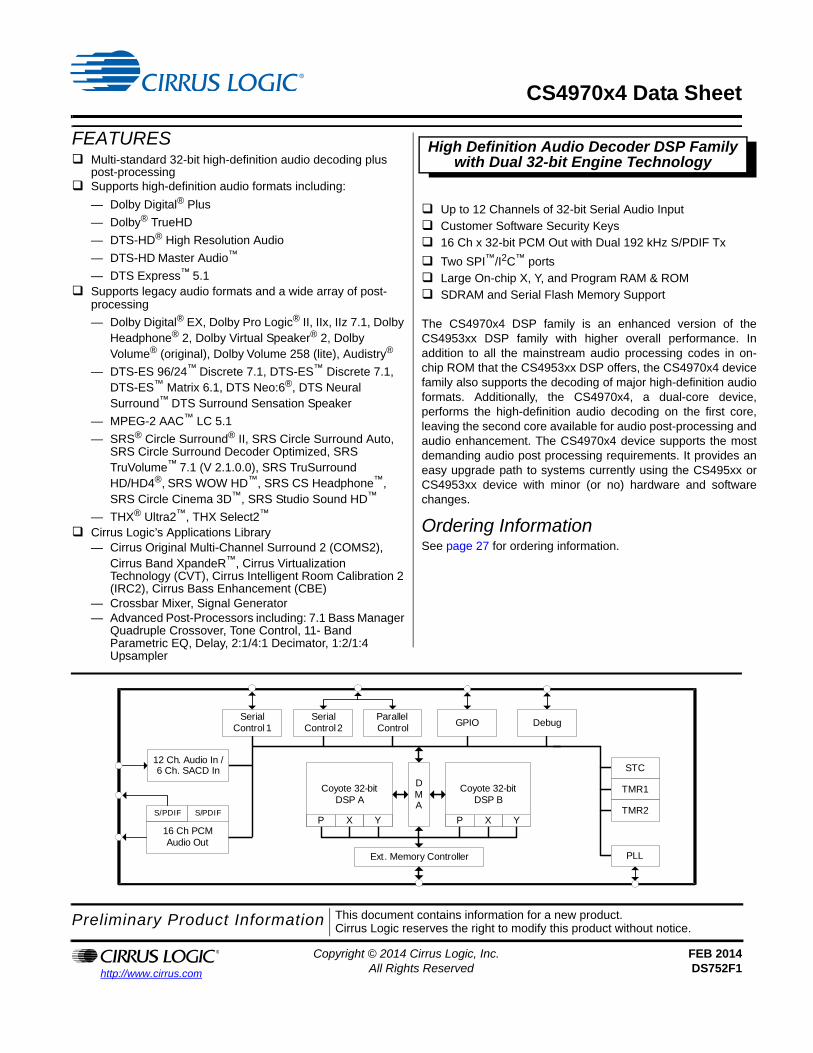
The CS4970x4 DSP family is an enhanced version of theCS4953xx DSP family with higher overall performance. Inaddition to all the mainstream audio processing codes in on-chip ROM that the CS4953xx DSP offers, the CS4970x4 devicefamily also supports the decoding of major high-definition audioformats. Additionally, the CS4970x4, a dual-core device,performs the high-definition audio decoding on the first core,leaving the second core available for audio post-processing andaudio enhancement. The CS4970x4 device supports the mostdemanding audio post processing requirements. It provides aneasy upgrade path to systems currently using the CS495xx orCS4953xx device with minor (or no) hardware and softwarechanges.
Ordering InformationSee page 27 for ordering information.
FEATURES Multi-standard 32-bit high-definition audio decoding plus
post-processing Supports high-definition audio formats including:
— Dolby Digital® Plus
— Dolby® TrueHD
— DTS-HD® High Resolution Audio
— DTS-HD Master Audio™
— DTS Express™ 5.1 Supports legacy audio formats and a wide array of post-
processing
— Dolby Digital® EX, Dolby Pro Logic® II, IIx, IIz 7.1, Dolby Headphone® 2, Dolby Virtual Speaker® 2, Dolby
Volume® (original), Dolby Volume 258 (lite), Audistry®
— DTS-ES 96/24™ Discrete 7.1, DTS-ES™ Discrete 7.1, DTS-ES™ Matrix 6.1, DTS Neo:6®, DTS Neural Surround™ DTS Surround Sensation Speaker
— MPEG-2 AAC™ LC 5.1
— SRS® Circle Surround® II, SRS Circle Surround Auto, SRS Circle Surround Decoder Optimized, SRS TruVolume™ 7.1 (V 2.1.0.0), SRS TruSurround HD/HD4®, SRS WOW HD™, SRS CS Headphone™, SRS Circle Cinema 3D™, SRS Studio Sound HD™
— THX® Ultra2™, THX Select2™
Cirrus Logic’s Applications Library— Cirrus Original Multi-Channel Surround 2 (COMS2),
Cirrus Band XpandeR™, Cirrus Virtualization Technology (CVT), Cirrus Intelligent Room Calibration 2 (IRC2), Cirrus Bass Enhancement (CBE)
— Crossbar Mixer, Signal Generator— Advanced Post-Processors including: 7.1 Bass Manager
Quadruple Crossover, Tone Control, 11- Band Parametric EQ, Delay, 2:1/4:1 Decimator, 1:2/1:4 Upsampler
Copyright © 2014 Cirrus Logic, Inc. FEB 2014All Rights Reserved DS752F1
Preliminary Product Information This document contains information for a new product.Cirrus Logic reserves the right to modify this product without notice.
http://www.cirrus.com
Coyote 32-bitDSP A
DMA
Coyote 32-bitDSP B
Ext. Memory Controller
PS/PDIF
X Y P X Y
SerialControl 1
16 Ch PCMAudio Out
SerialControl 2
ParallelControl GPIO Debug
STC
TMR1
TMR2
PLL
S/PDIF
12 Ch. Audio In / 6 Ch. SACD In

CS4970x4 Data Sheet32-bit High Definition Audio Decoder DSP Family
Table of Contents
1 Documentation Strategy ............................................................................................................4
2 Overview .....................................................................................................................................42.1 Migrating from CS495xx(3) to CS4970x4 ................................................................................................. 52.2 Licensing .................................................................................................................................................. 5
3 Code Overlays ............................................................................................................................5
4 Hardware Functional Description ............................................................................................64.1 Coyote DSP Core ..................................................................................................................................... 6
4.1.1 DSP Memory ...............................................................................................................................64.1.2 DMA Controller ............................................................................................................................7
4.2 On-chip DSP Peripherals ......................................................................................................................... 74.2.1 Digital Audio Input Port (DAI) .......................................................................................................74.2.2 Digital Audio Output Port (DAO) ..................................................................................................74.2.3 Serial Control Port 1 & 2 (I2C or SPI) ..........................................................................................74.2.4 External Memory Interface ..........................................................................................................74.2.5 General Purpose Input/Output (GPIO) ........................................................................................74.2.6 Phase-locked Loop (PLL)-based Clock Generator ......................................................................7
4.3 DSP I/O Description ................................................................................................................................. 84.3.1 Multiplexed Pins ..........................................................................................................................84.3.2 Termination Requirements ...........................................................................................................84.3.3 Pads ............................................................................................................................................8
4.4 Application Code Security ........................................................................................................................ 8
5 Characteristics and Specifications ..........................................................................................85.1 Absolute Maximum Ratings ...................................................................................................................... 85.2 Recommended Operating Conditions ...................................................................................................... 95.3 Digital DC Characteristics ........................................................................................................................ 95.4 Power Supply Characteristics .................................................................................................................. 95.5 Thermal Data (128-pin LQFP) ................................................................................................................ 105.6 Switching Characteristics—RESET ......................................................................................................... 115.7 Switching Characteristics — XTI ............................................................................................................ 115.8 Switching Characteristics — Internal Clock ............................................................................................ 125.9 Switching Characteristics — Serial Control Port - SPI Slave Mode ....................................................... 135.10 Switching Characteristics — Serial Control Port - SPI Master Mode ................................................... 145.11 Switching Characteristics — Serial Control Port - I2C Slave Mode ...................................................... 155.12 Switching Characteristics — Serial Control Port - I2C Master Mode .................................................... 165.13 Switching Characteristics — Parallel Control Port - Intel Slave Mode ................................................. 165.14 Switching Characteristics — Parallel Control Port - Motorola Slave Mode ......................................... 195.15 Switching Characteristics — Digital Audio Slave Input Port ................................................................. 215.16 Switching Characteristics — Digital Audio Output Port ........................................................................ 225.17 Switching Characteristics — SDRAM Interface .................................................................................... 23
6 Ordering Information ...............................................................................................................27
7 Environmental, Manufacturing, and Handling Information .................................................27
8 Device Pin-Out Diagram ..........................................................................................................288.1 128-Pin LQFP Pin-Out Diagram ............................................................................................................. 28
9 Package Mechanical Drawings ...............................................................................................299.1 128-Pin LQFP Package Drawing ........................................................................................................... 29
10 Revision History .....................................................................................................................30
DS752F1 2

CS4970x4 Data Sheet32-bit High Definition Audio Decoder DSP Family
List of Figures
Figure 1. RESET Timing .........................................................................................................................................11Figure 2. XTI Timing ..............................................................................................................................................11Figure 3. Serial Control Port - SPI Slave Mode Timing ..........................................................................................13Figure 4. Serial Control Port - SPI Master Mode Timing ........................................................................................14Figure 5. Serial Control Port - I2C Slave Mode Timing ..........................................................................................15Figure 6. Serial Control Port - I2C Master Mode Timing ........................................................................................16Figure 7. Parallel Control Port - IntelÒ Slave Mode Read Cycle ...........................................................................17Figure 8. Parallel Control Port - Intel Slave Mode Write Cycle ..............................................................................18Figure 9. Parallel Control Port - MotorolaÒ Slave Mode Read Cycle Timing ........................................................20Figure 10. Parallel Control Port - Motorola Slave Mode Write Cycle Timing .........................................................20Figure 11. Digital Audio Input (DAI) Port Timing Diagram .....................................................................................21Figure 12. DAI Slave Timing Diagram ...................................................................................................................21Figure 13. Digital Audio Port Output Timing Master Mode .....................................................................................22Figure 14. Digital Audio Output Timing, Slave Mode (Relationship LRCLK to SCLK) ...........................................23Figure 15. External Memory Interface - SDRAM Burst Read Cycle .......................................................................24Figure 16. External Memory Interface - SDRAM Burst Write Cycle .......................................................................24Figure 17. External Memory Interface - SDRAM Auto Refresh Cycle ....................................................................25Figure 18. External Memory Interface - SDRAM Load Mode Register Cycle ........................................................26Figure 19. 128-Pin LQFP Pin-Out Diagram ...........................................................................................................28Figure 20. 128-Pin LQFP Package Drawing ..........................................................................................................29
List of Tables
Table 1. CS4970x4 Related Documentation . . . . . . . . . . . . . . . . . . . . . . . . . . . . . . . . . . . . . . . . . . . . . . . . . . . . . . 4Table 2. Device and Firmware Selection Guide. . . . . . . . . . . . . . . . . . . . . . . . . . . . . . . . . . . . . . . . . . . . . . . . . . . . 5Table 3. CS4970x4 DSP Memory Sizes . . . . . . . . . . . . . . . . . . . . . . . . . . . . . . . . . . . . . . . . . . . . . . . . . . . . . . . . . 7Table 4. Ordering Information . . . . . . . . . . . . . . . . . . . . . . . . . . . . . . . . . . . . . . . . . . . . . . . . . . . . . . . . . . . . . . . . 27Table 5. Environmental, Manufacturing, & Handling Information. . . . . . . . . . . . . . . . . . . . . . . . . . . . . . . . . . . . . . 27Table 6. 128-Pin LQFP Package Characteristics . . . . . . . . . . . . . . . . . . . . . . . . . . . . . . . . . . . . . . . . . . . . . . . . . 29
DS752F1 3
CS4970x4 Data Sheet32-bit High Definition Audio Decoder DSP Family
1 Documentation StrategyThe CS4970x4 data sheet describes the CS4970x4 family of multichannel audio decoders. This documentshould be used in conjunction with the following documents when evaluating or designing a system around theCS4970x4 family of processors.
The scope of the CS4970x4 data sheet is primarily to provide hardware specifications of the CS4970x4 familyof devices. This includes hardware functionality, characteristic data, pinout, and packaging information.
The intended audience for the CS4970x4 data sheet is the system PCB designer, MCU programmer, and thequality control engineer.
2 OverviewThe CS4970x4 DSP Family, combined with Cirrus Logic’s comprehensive library of audio processingalgorithms, enables the development of next-generation high-definition audio solutions. Cirrus Logic alsoprovides a broad array of digital interface products and audio converters to meet your audio system-leveldesign requirements.
Note: The CS4970x4 is available in a 128-pin LQFP package.
The audio processing features of the CS4970x4 product family are a superset of audio features available inthe CS4953xx product family.
Refer to Table 2 on page 5 for the speed and firmware features of the CS4970x4 product family.
Table 1. CS4970x4 Related Documentation
Document Name Description
CS4970x4 Data Sheet This document
CS495314/CS4970x4 System Designer’s Guide
A new consolidated documentation set that includes:
• Detailed system design information including Typical Connection Diagrams, Boot-Procedures, Pin Descriptions, Etc. Also describes use of DSP Condenser tool.
• Detailed firmware design information including signal processing flow diagrams and control API information
AN288 - CS4953xx/CS4970x4 Firmware User’s ManualIncludes detailed firmware design information including signal processing flow diagrams and control API information
DS752F1 4

CS4970x4 Data Sheet32-bit High Definition Audio Decoder DSP Family
2.1 Migrating from CS495xx(3) to CS4970x4
CS4970x4 was designed to provide an easy upgrade path from the CS495xx and CS4953x. There are somesmall differences the hardware designer should be aware of:
• The PLL supply voltage on the CS4970x4 is 3.3V vs. 1.8V on the CS495xx.
• The PLL filter topology is simpler when using the CS4970x4 rather than the CS495xx.
• The CS4970x4 adds support for Time-division multiplexing (TDM) mode on both audio input and output ports.
• The CS4970x4 does not support external static random access memory (SRAM) operation.
• The CS4970x4 external Synchronous dynamic random access memory (SDRAM) bus speed is fixed at 150 MHz vs. the 120 MHz maximum bus speed for the CS495xx. Some firmware modules also support a 75 MHz CS4970x4 SDRAM bus speed. Refer to AN304 for details.
• The CS4970x4 CLKOUT pin can output XTALI or XTALI/2. The CS495xx can only output XTALI.
2.2 Licensing
Licenses are required for all of the third party audio decoding/processing algorithms listed below, including theapplication notes. Contact your local Cirrus Sales representative for more information.
3 Code OverlaysThe suite of software available for the CS4970x4 family consists of operating systems (OS) and a library ofoverlays. The overlays have been divided into three main groups: decoders, matrix processors, andpostprocessors. All software components are defined in the following list:
Table 2. Device and Firmware Selection Guide
DeviceDecode Processor
(DSP-A)1Matrix Processor Module
(DSP-A)1
1. Additional processing (MPMA, MPMB/VPM, PPM) post any of the HD audio decoders may be limited. Contact your Cirrus Logic FAE for the latest concurrency matrix.
Virtualizer Processor Module
(DSP-B)1
Post Processor Module
(DSP-B)1
CS497014300MACS
Stereo PCM(4:1/2:1 Down-sampling and
1:2/1:4 U-sampling Options)2
Multichannel PCM(4:1/2:1 Down-sampling and
1:2/1:4 Up-sampling Options)2
Dolby DigitalMPEG-2 AAC LC 5.1
Dolby Digital Plus
Dolby TrueHD3
2. Downsampling and Upsampling functionality is located in the operating system. The Cirrus Decimator (Down-Sampler) is also available as a separate post-processing module that is described in the application note AN288PPI.
3. The indicated HD audio decoder algorithms require external SDRAM. Consult your Cirrus Logic FAE for the recommended SDRAM size for your design.
Dolby Pro Logic II / IIx / IIz 7.1
SRS Circle Surround II / Circle Surround Auto / Circle
Surround Decoder Optimized (Stereo In)
Cirrus Original Multi-Channel Surround 2 (Effects / Reverb
Processor)
Crossbar (Down-mix / Up-mix)(Simultaneous Process)
Cirrus Virtualizer Technology
Dolby Headphone 2
Dolby Virtual Speaker 2
SRS CS Headphone
SRS TruSurround HD/HD4
APP (Advanced Post-processing)
–Tone Control–Select 2–PEQ (up to 11 Bands)–Delay
(Speaker to Listening Position Alignment and/or Lip Sync)–7.1 Bass Manager–Audio Manager
–4:1/2:1 Down-sampling2
SRS TruVolume 7.1Multichannel
Dolby Volume Multichannel
CS497004300MACS
CS497024300MACS
Same as CS497014 +DTS, DTS-ES, DTS96/24
DTS-HD Master Audio3
DTS-HD High Res Audio3
DTS Express 5.1
Same as CS497014 +DTS Neo:6, DTS Neural
Surround
DS752F1 5

CS4970x4 Data Sheet32-bit High Definition Audio Decoder DSP Family
• OS/Kernel - Encompasses all non-audio processing tasks, including loading data from external memory, processing host messages, calling audio-processing subroutines, auto-detection, error concealment, etc.
• Decoders - Any module that initially writes data into the audio I/O buffers, e.g. AC-3™, DTS, PCM, etc. All the decoding/processing algorithms listed require delivery of PCM or IEC61937-packed, compressed data via I2S- or LJ-formatted digital audio to the CS4970x4 from A/D converters, SPDIF Rx, HDMI Rx, etc.
• Matrix-processors - Any module that processes audio I/O buffer PCM data in-place before the Post-processors. Generally speaking, these modules alter the number of valid channels in the audio I/O buffer through processes like Virtualization (n2 channels) or Matrix Decoding (2n channels). Examples are Dolby ProLogic IIx and DTS Neo:6.
• Virtualizer-processor - Any module that encodes PCM data into fewer output channels than input channels (n2 channels) with the effect of providing “phantom” speakers to represent the physical audio channels that were eliminated. Examples are Dolby Headphone 2 and Dolby Virtual Speaker 2. Generally speaking, these modules reduce the number of valid channels in the audio I/O buffer.
• Post-processors - Any module that processes audio I/O buffer PCM data in-place after the matrix processors. Examples are bass management, audio manager, tone control, EQ, delay, customer-specific effects, Dolby Headphone/Virtual Speaker, etc.
The overlay structure reduces the time required to reconfigure the DSP when a processing change isrequested. Each overlay can be reloaded independently without disturbing the other overlays. For example,when a new decoder is selected, the OS, matrix-, and post-processors do not need to be reloaded — only thenew decoder (the same is true for the other overlays).
4 Hardware Functional Description
4.1 Coyote DSP Core
The CS4970x4 is a dual-core Coyote DSP with separate X and Y data and P code memory spaces. Each coreis a high-performance, 32-bit, user-programmable, fixed-point DSP that is capable of performing two multiplyaccumulate (MAC) operations per clock cycle. Each core has eight 72-bit accumulators, four X- and four Y-dataregisters, and 12 index registers.
Both DSP cores are coupled to a flexible DMA engine. The DMA engine can move data between peripheralssuch as the digital audio input (DAI) and digital audio output (DAO), external memory, or any DSP corememory, all without the intervention of the DSP. The DMA engine offloads data move instructions from the DSPcore, leaving more MIPS available for signal processing instructions.
CS4970x4 functionality is controlled by application codes that are stored in on-board ROM or downloaded tothe CS4970x4 from a host MCU or external FLASH/EEPROM. Users can choose to use standard audiodecoder and post-processor modules which are available from Cirrus Logic.
The CS4970x4 is suitable for audio decoder, audio post-processor, audio encoder, DVD audio/video player,and digital broadcast decoder applications.
4.1.1 DSP Memory
Each DSP core has its own on-chip data and program RAM and ROM and does not require external memoryfor any of today’s popular audio algorithms including Dolby Digital Surround EX, AAC Multichannel, DTS-ES96/24, and THX Ultra2. However, if the end-system design requires support of the new high-definition audioformats, external SDRAM will be needed to support Dolby TrueHD and DTS-HD master audio.
The memory maps for the DSPs are as follows. All memory sizes are composed of 32-bit words.
DS752F1 6

CS4970x4 Data Sheet32-bit High Definition Audio Decoder DSP Family
4.1.2 DMA Controller
The powerful 12-channel DMA controller can move data between 8 on-chip resources. Each resource has itsown arbiter: X, Y, and P RAM/ROMs on DSP A; X, Y, and P RAM/ROMs on DSP B; external memory; and theperipheral bus. Modulo and linear addressing modes are supported, with flexible start address and incrementcontrols. The service interval for each DMA channel as well as up to 6 interrupt events, is programmable.
4.2 On-chip DSP Peripherals
4.2.1 Digital Audio Input Port (DAI)
The 12-channel (6-line) DAI port supports a wide variety of data input formats. The port is capable of acceptingPCM or IEC61937. Up to 32-bit word lengths are supported. Additionally, support is provided for audio datainput to the DSP via the DAI from an HDMI receiver.
The port has two independent slave-only clock domains. Each data input can be independently assigned to aclock domain. The sample rate of the input clock domains can be determined automatically by the DSP, whichoff-loads the task of monitoring the SPDIF receiver from the host. A time-stamping feature allows the input datato be sample-rate converted via software.
4.2.2 Digital Audio Output Port (DAO)
There are two DAO ports. Each port can output 8 channels of up to 32-bit PCM data. The port supports datarates from 32 kHz to 192 kHz. Each port can be configured as an independent clock domain in slave mode, orthe ratio of the two clocks can be set to even multiples of each other in master mode. The two ports can also beganged together into a single clock domain. Each port has one serial audio pin that can be configured as a192-kHz SPDIF transmitter (data with embedded clock on a single line).
4.2.3 Serial Control Port 1 & 2 (I2C or SPI)
There are two on-chip serial control ports that are capable of operating as master or slave in either I2C or SPImodes. SCP1 defaults to slave operation. It is dedicated for external host-control and supports an externalclock up to 50 MHz in SPI mode. This high clock speed enables very fast code download, control or datadelivery. SCP2 defaults to master mode and is dedicated for booting from external serial Flash memory or foraudio sub-system control.
4.2.4 External Memory Interface
The external memory interface controller supports up to 128 Mbits of SDRAM, using a 16-bit data bus.
4.2.5 General Purpose Input/Output (GPIO)
Many of the CS4970x4 peripheral pins are multiplexed with GPIO. Each GPIO can be configured as an output,an input, or an input with interrupt. Each input-pin interrupt can be configured as rising edge, falling edge,active-low, or active-high.
4.2.6 Phase-locked Loop (PLL)-based Clock Generator
The low-jitter PLL generates integer or fractional multiples of a reference frequency which are used to clock theDSP core and peripherals. Through a second PLL divider chain, a dependent clock domain can be output onthe DAO port for driving audio converters. The CS4970x4 defaults to running from the external referencefrequency and can be switched to use the PLL output after overlays have been loaded and configured, either
Table 3. CS4970x4 DSP Memory Sizes
Memory Type
DSP A DSP B
X 16K SRAM, 32K ROM 10K SRAM, 8K ROM
Y 24K SRAM, 32K ROM 16K SRAM, 16K ROM
P 8K SRAM, 32K ROM 8K SRAM, 24K ROM
DS752F1 7

CS4970x4 Data Sheet32-bit High Definition Audio Decoder DSP Family
through master boot from an external FLASH or through host control. A built-in crystal oscillator circuit with abuffered output is provided. The buffered output frequency ratio is selectable between 1:1 (default) or 2:1.
4.3 DSP I/O Description
4.3.1 Multiplexed Pins
Many of the CS4970x4 pins are multi-functional. For details on pin functionality please refer to the CS4970x4System Designer’s Guide.
4.3.2 Termination Requirements
Open-drain pins on the CS4970x4 must be pulled high for proper operation. Please refer to the CS4970x4System Designer’s Guide to identify which pins are open-drain and what value of pull-up resistor is required forproper operation.
Mode select pins on the CS4970x4 are used to select the boot mode upon the rising edge of reset. A detailedexplanation of termination requirements for each communication mode select pin can be found in theCS4970x4 System Designer’s Guide.
4.3.3 Pads
The CS4970x4 I/O operates from the 3.3 V supply and is tolerant within 5 V.
4.4 Application Code Security
The external program code may be encrypted by the programmer to protect any intellectual property it maycontain. A secret, customer-specific key is used to encrypt the program code that is to be stored external to thedevice.
5 Characteristics and SpecificationsNote: All data sheet minimum and maximum timing parameters are guaranteed over the rated voltage
and temperature. All data sheet typical parameters are measured under the following conditions: T = 25 °C, CL = 20 pF, VDD = 1.8 V, VDDA = VDDIO = 3.3 V, GNDD = GNDIO = GNDA = 0 V.
5.1 Absolute Maximum Ratings(GNDD = GNDIO = GNDA = 0 V; all voltages with respect to 0 V)
CAUTION: Operation at or beyond these limits may result in permanent damage to the device. Normal operation isnot guaranteed at these extremes.
Parameter Symbol Min Max Unit
DC power supplies: Core supplyPLL supplyI/O supply
|VDDA – VDDIO|
VDDVDDAVDDIO
–0.3–0.3–0.3—
2.03.63.60.3
VVVV
Input pin current, any pin except supplies Iin — +/- 10 mA
Input voltage on PLL_REF_RES Vfilt -0.3 3.6 V
Input voltage on I/O pins Vinio -0.3 5.0 V
Storage temperature Tstg -65 150 °C
DS752F1 8
CS4970x4 Data Sheet32-bit High Definition Audio Decoder DSP Family
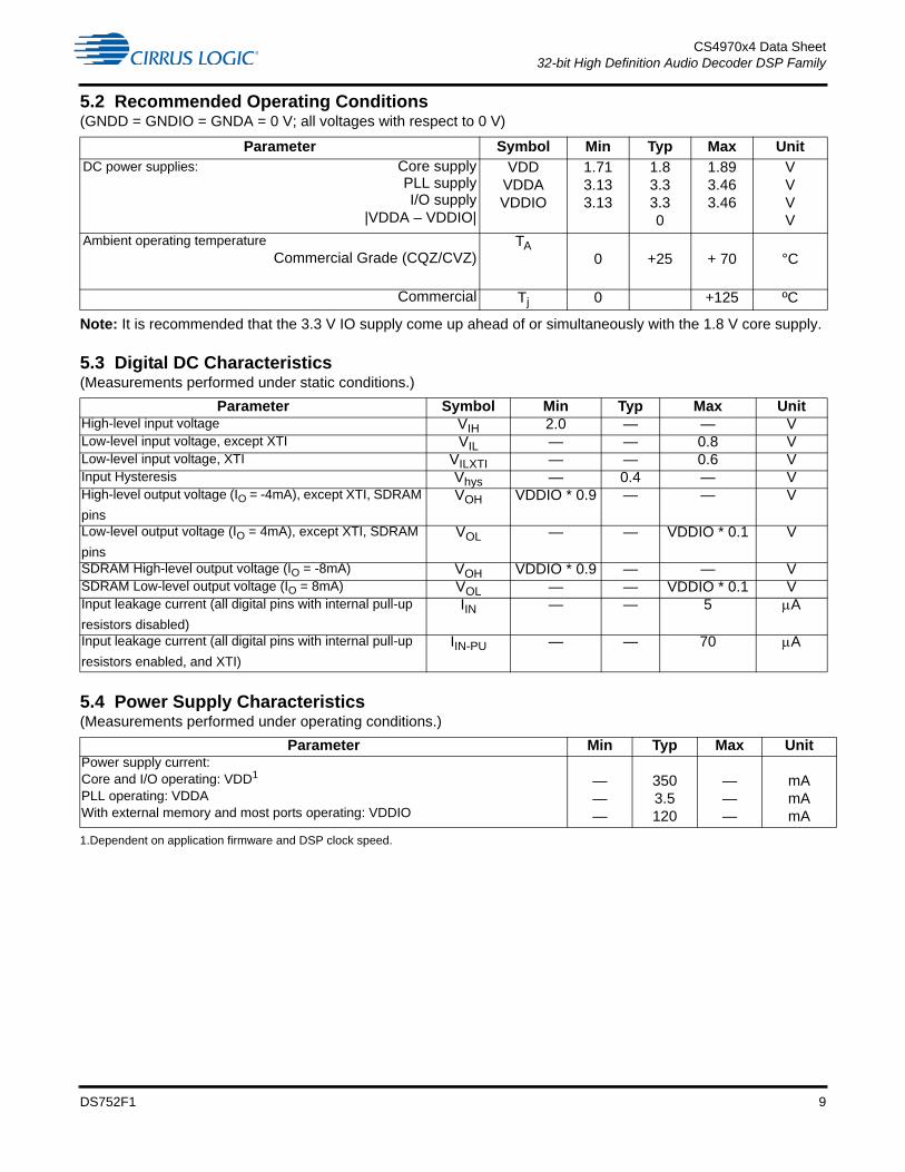
5.2 Recommended Operating Conditions(GNDD = GNDIO = GNDA = 0 V; all voltages with respect to 0 V)
Note: It is recommended that the 3.3 V IO supply come up ahead of or simultaneously with the 1.8 V core supply.
5.3 Digital DC Characteristics(Measurements performed under static conditions.)
5.4 Power Supply Characteristics(Measurements performed under operating conditions.)
Parameter Symbol Min Typ Max UnitDC power supplies: Core supply
PLL supplyI/O supply
|VDDA – VDDIO|
VDDVDDAVDDIO
1.713.133.13
1.83.33.30
1.893.463.46
VVVV
Ambient operating temperatureCommercial Grade (CQZ/CVZ)
TA0 +25 + 70
°C
Commercial Tj 0 +125 ºC
Parameter Symbol Min Typ Max UnitHigh-level input voltage VIH 2.0 — — VLow-level input voltage, except XTI VIL — — 0.8 VLow-level input voltage, XTI VILXTI — — 0.6 VInput Hysteresis Vhys — 0.4 — VHigh-level output voltage (IO = -4mA), except XTI, SDRAM
pins
VOH VDDIO * 0.9 — — V
Low-level output voltage (IO = 4mA), except XTI, SDRAM
pins
VOL — — VDDIO * 0.1 V
SDRAM High-level output voltage (IO = -8mA) VOH VDDIO * 0.9 — — VSDRAM Low-level output voltage (IO = 8mA) VOL — — VDDIO * 0.1 VInput leakage current (all digital pins with internal pull-up
resistors disabled)
IIN — — 5 A
Input leakage current (all digital pins with internal pull-up
resistors enabled, and XTI)
IIN-PU — — 70 A
Parameter Min Typ Max UnitPower supply current:Core and I/O operating: VDD1
PLL operating: VDDAWith external memory and most ports operating: VDDIO
1.Dependent on application firmware and DSP clock speed.
———
3503.5120
———
mAmAmA
DS752F1 9

CS4970x4 Data Sheet32-bit High Definition Audio Decoder DSP Family
5.5 Thermal Data (128-pin LQFP)
Notes: 1. Two-layer board is specified as a 76 mm X 114 mm, 1.6 mm thick FR-4 material with 1-oz. copper covering 20% of the top and bottom layers.
2. Four-layer board is specified as a 76 mm X 114 mm, 1.6 mm thick FR-4 material with 1-oz. copper covering 20% of the top and bottom layers and 0.5-oz. copper covering 90% of the internal power plane and ground plane layers.
3. To calculate the die temperature for a given power dissipation
j = Ambient Temperature + [ (Power Dissipation in Watts) * ja ]
4. To calculate the case temperature for a given power dissipation
c = j - [ (Power Dissipation in Watts) * jt
Parameter Symbol Min Typ Max Unit
Thermal Resistance (Junction to Ambient)
Two-layer Board1
Four-layer Board2
ja——
5344
——
°C / Watt
Thermal Resistance (Junction to Top of Package)
Two-layer Board1
Four-layer Board2
jt——
.45
.39——
°C / Watt
DS752F1 10

CS4970x4 Data Sheet32-bit High Definition Audio Decoder DSP Family
5.6 Switching Characteristics—RESET
Figure 1. RESET Timing
5.7 Switching Characteristics — XTI
Figure 2. XTI Timing
Parameter Symbol Min Max Unit
RESET minimum pulse width low Trstl 1 — s
All bidirectional pins high-Z after RESET low Trst2z — 100 ns
Configuration pins setup before RESET high Trstsu 50 — ns
Configuration pins hold after RESET high Trsthld 20 — ns
Parameter Symbol Min Max Unit
External Crystal operating frequency1
1. Part characterized with the following crystal frequency values: 12.288 and 24.576 MHz.
Fxtal 12.288 24.576 MHz
XTI period Tclki 41 81.4 ns
XTI high time Tclkih 16.4 — ns
XTI low time Tclkil 16.4 — ns
External Crystal Load Capacitance (parallel resonant)2
2. CL refers to the total load capacitance as specified by the crystal manufacturer. Crystals which require a CL outside this range
should be avoided. The crystal oscillator circuit design should follow the crystal manufacturer’s recommendation for load capacitor selection.
CL 10 18 pF
External Crystal Equivalent Series Resistance ESR — 50
RESET#
Trst2z
Trstl
Trstsu Trsthld
HS[3:0]
All BidirectionalPins
t clkih t clkil
Tclki
XTI
DS752F1 11

CS4970x4 Data Sheet32-bit High Definition Audio Decoder DSP Family
5.8 Switching Characteristics — Internal Clock
Parameter Symbol Min Max Unit
Internal DCLK frequency1
1. After initial power-on reset, Fdclk = Fxtal. After initial kick-start commands, the PLL is locked to max Fdclk and remains locked until
the next power-on reset.
Fdclk — – MHz
CS497004-CQZCS497004-CQZR
CS497024-CVZCS497024-CVZR
CS497014-CVZCS497014-CVZR
CS497024-CVZCS497024-CVZR
Fxtal 131
Internal DCLK period1 DCLKP — – ns
CS497004-CQZCS497004-CQZR
CS497024-CVZCS497024-CVZR
CS497014-CVZCS497014-CVZR
CS497024-CVZCS497024-CVZR
7.63 1/Fxtal
DS752F1 12
CS4970x4 Data Sheet32-bit High Definition Audio Decoder DSP Family
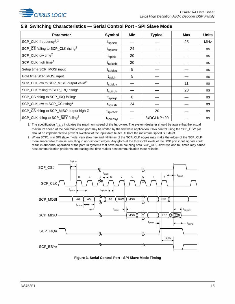
5.9 Switching Characteristics — Serial Control Port - SPI Slave Mode
Figure 3. Serial Control Port - SPI Slave Mode Timing
Parameter Symbol Min Typical Max Units
SCP_CLK frequency1,2
1. The specification fspisck indicates the maximum speed of the hardware. The system designer should be aware that the actual
maximum speed of the communication port may be limited by the firmware application. Flow control using the SCP_BSY pin should be implemented to prevent overflow of the input data buffer. At boot the maximum speed is Fxtal/3.
2. When SCP1 is in SPI slave mode, very slow rise and fall times of the SCP_CLK edges may make the edges of the SCP_CLK more susceptible to noise, resulting in non-smooth edges. Any glitch at the threshold levels of the SCP port input signals could result in abnormal operation of the port. In systems that have noise coupling onto SCP_CLK, slow rise and fall times may cause host communication problems. Increasing rise time makes host communication more reliable.
fspisck — — 25 MHz
SCP_CS falling to SCP_CLK rising2 tspicss 24 — — ns
SCP_CLK low time2 tspickl 20 — — ns
SCP_CLK high time2 tspickh 20 — — ns
Setup time SCP_MOSI input tspidsu 5 — — ns
Hold time SCP_MOSI input tspidh 5 — — ns
SCP_CLK low to SCP_MISO output valid2 tspidov — — 11 ns
SCP_CLK falling to SCP_IRQ rising2 tspiirqh — — 20 ns
SCP_CS rising to SCP_IRQ falling2 tspiirql 0 — — ns
SCP_CLK low to SCP_CS rising2 tspicsh 24 — — ns
SCP_CS rising to SCP_MISO output high-Z tspicsdz — 20 — ns
SCP_CLK rising to SCP_BSY falling2 tspicbsyl — 3*DCLKP+20 — ns
SCP_BSY#
SCP_CS#
SCP_CLK
SCP_MOSI
SCP_MISO
SCP_IRQ#
0 1 2 6 7 0 5 6 7
tspicss
tspickl
tspickh
tspidsu
tspidh tspidov
A6 A5 A0 R/W MSB LSB
MSB LSB
tspicsh
tspibsyl
tspiirqltspiirqh
fspisck
tspicsdz
DS752F1 13

CS4970x4 Data Sheet32-bit High Definition Audio Decoder DSP Family
5.10 Switching Characteristics — Serial Control Port - SPI Master Mode
.
Figure 4. Serial Control Port - SPI Master Mode Timing
Parameter Symbol Min Typical Max Units
SCP_CLK frequency1, 2
1. The specification fspisck indicates the maximum speed of the hardware. The system designer should be aware that the actual
maximum speed of the communication port may be limited by the firmware application. 2. See Section 5.7.3. SCP_CLK PERIOD refers to the period of SCP_CLK as being used in a given application. It does not refer to a tested parameter.
fspisck — — Fxtal/2 MHz
SCP_CS falling to SCP_CLK rising 3 tspicss — 11*DCLKP + (SCP_CLK PERIOD)/2
— ns
SCP_CLK low time tspickl 16.9 — — ns
SCP_CLK high time tspickh 16.9 — — ns
Setup time SCP_MISO input tspidsu 11 — — ns
Hold time SCP_MISO input tspidh 5 — — ns
SCP_CLK low to SCP_MOSI output valid tspidov — — 11 ns
SCP_CLK low to SCP_CS falling tspicsl 7 — — ns
SCP_CLK low to SCP_CS rising tspicsh — 11*DCLKP + (SCP_CLK PERIOD)/2
— ns
Bus free time between active SCP_CS tspicsx — 3*DCLKP — ns
SCP_CLK falling to SCP_MOSI output high-Z tspidz — — 20 ns
EE_CS#
SCP_CLK
SCP_MISO
SCP_MOSI
0 1 2 6 7 0 5 6 7
tspicss
tspickl
tspickh
tspidsu
tspidh tspidov
A6 A5 A0 R/W MSB LSB
MSB LSB
tspicsh
tspicsx
fspisck
tspidz
tspicsl
DS752F1 14

CS4970x4 Data Sheet32-bit High Definition Audio Decoder DSP Family
5.11 Switching Characteristics — Serial Control Port - I2C Slave Mode
Figure 5. Serial Control Port - I2C Slave Mode Timing
Parameter Symbol Min Typical Max Units
SCP_CLK frequency1
1. The specification fiicck indicates the maximum speed of the hardware. The system designer should be aware that the actual
maximum speed of the communication port may be limited by the firmware application. Flow control using the SCP_BSY pin should be implemented to prevent overflow of the input data buffer.
fiicck — — 400 kHz
SCP_CLK low time tiicckl 1.25 — — µs
SCP_CLK high time tiicckh 1.25 — — µs
SCP_SCK rising to SCP_SDA rising or falling for START or
STOP condition
tiicckcmd 1.25 — — µs
START condition to SCP_CLK falling tiicstscl 1.25 — — µs
SCP_CLK falling to STOP condition tiicstp 2.5 — — µs
Bus free time between STOP and START conditions tiicbft 3 — — µs
Setup time SCP_SDA input valid to SCP_CLK rising tiicsu 100 — — ns
Hold time SCP_SDA input after SCP_CLK falling2
2. This parameter is measured from the ViL level at the falling edge of the clock.
tiich 0 — — ns
SCP_CLK low to SCP_SDA out valid tiicdov — — 18 ns
SCP_CLK falling to SCP_IRQ rising tiicirqh — — 3*DCLKP + 40 ns
NAK condition to SCP_IRQ low tiicirql — 3*DCLKP + 20 — ns
SCP_CLK rising to SCB_BSY low tiicbsyl — 3*DCLKP + 20 — ns
SCP_BSY#
SCP_CLK
SCP_SDA
SCP_IRQ#
0 1 6 7 8 0 1 7
tiicckl
tiicckh
tiicsu tiich
A6 A0 R/W ACK LSB
tiicirqh tiicirql
8
ACKMSB
tiicstp
6
tiiccbsyl
tiicdov tiicbfttiicstscl
tiicckcmd
fiicck
tiicckcmdtiicftiicr
DS752F1 15
CS4970x4 Data Sheet32-bit High Definition Audio Decoder DSP Family
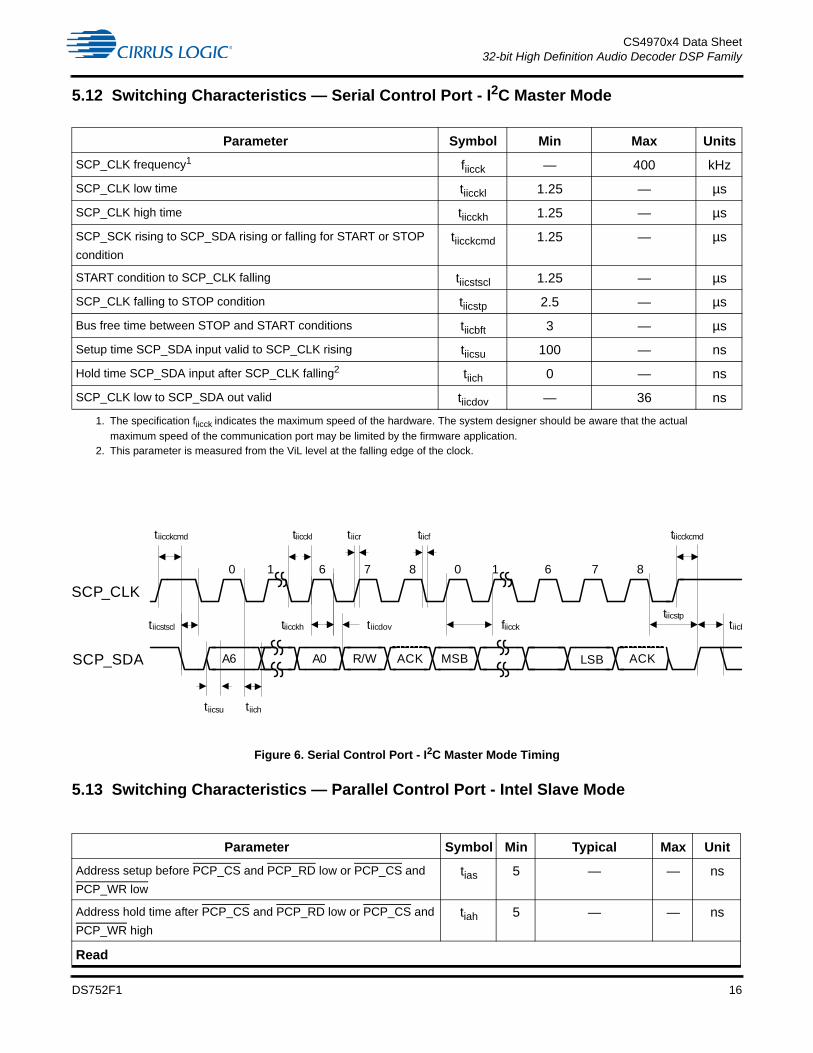
5.12 Switching Characteristics — Serial Control Port - I2C Master Mode
Figure 6. Serial Control Port - I2C Master Mode Timing
5.13 Switching Characteristics — Parallel Control Port - Intel Slave Mode
Parameter Symbol Min Max Units
SCP_CLK frequency1
1. The specification fiicck indicates the maximum speed of the hardware. The system designer should be aware that the actual
maximum speed of the communication port may be limited by the firmware application.
fiicck — 400 kHz
SCP_CLK low time tiicckl 1.25 — µs
SCP_CLK high time tiicckh 1.25 — µs
SCP_SCK rising to SCP_SDA rising or falling for START or STOP
condition
tiicckcmd 1.25 — µs
START condition to SCP_CLK falling tiicstscl 1.25 — µs
SCP_CLK falling to STOP condition tiicstp 2.5 — µs
Bus free time between STOP and START conditions tiicbft 3 — µs
Setup time SCP_SDA input valid to SCP_CLK rising tiicsu 100 — ns
Hold time SCP_SDA input after SCP_CLK falling2
2. This parameter is measured from the ViL level at the falling edge of the clock.
tiich 0 — ns
SCP_CLK low to SCP_SDA out valid tiicdov — 36 ns
Parameter Symbol Min Typical Max Unit
Address setup before PCP_CS and PCP_RD low or PCP_CS and
PCP_WR low
tias 5 — — ns
Address hold time after PCP_CS and PCP_RD low or PCP_CS and
PCP_WR high
tiah 5 — — ns
Read
SCP_CLK
SCP_SDA
0 1 6 7 8 0 1 7
tiicckl
tiicckh
tiicsu tiich
A6 A0 R/W ACK LSB
8
ACKMSB
tiicstp
6
tiicdov tiicbtiicstscl
tiicckcmd
fiicck
tiicckcmdtiicftiicr
DS752F1 16

CS4970x4 Data Sheet32-bit High Definition Audio Decoder DSP Family
Figure 7. Parallel Control Port - Intel Slave Mode Read Cycle
Delay between PCP_RD then PCP_CS low or PCP_CS then
PCP_RD low
ticdr 0 — — ns
Data valid after PCP_CS and PCP_RD low tidd — — 18 ns
PCP_CS and PCP_RD low for read tirpw 24 — — ns
Data hold time after PCP_CS or PCP_RD high tidhr 8 — — ns
Data high-Z after PCP_CS or PCP_RD high tidis — — 18 ns
PCP_CS or PCP_RD high to PCP_CS and PCP_RD low for next
read1tird 30 — — ns
PCP_CS or PCP_RD high to PCP_CS and PCP_WR low for next
write1tirdtw 30 — — ns
PCP_RD rising to PCP_IRQ rising tirdirqhl — — 12 ns
Write
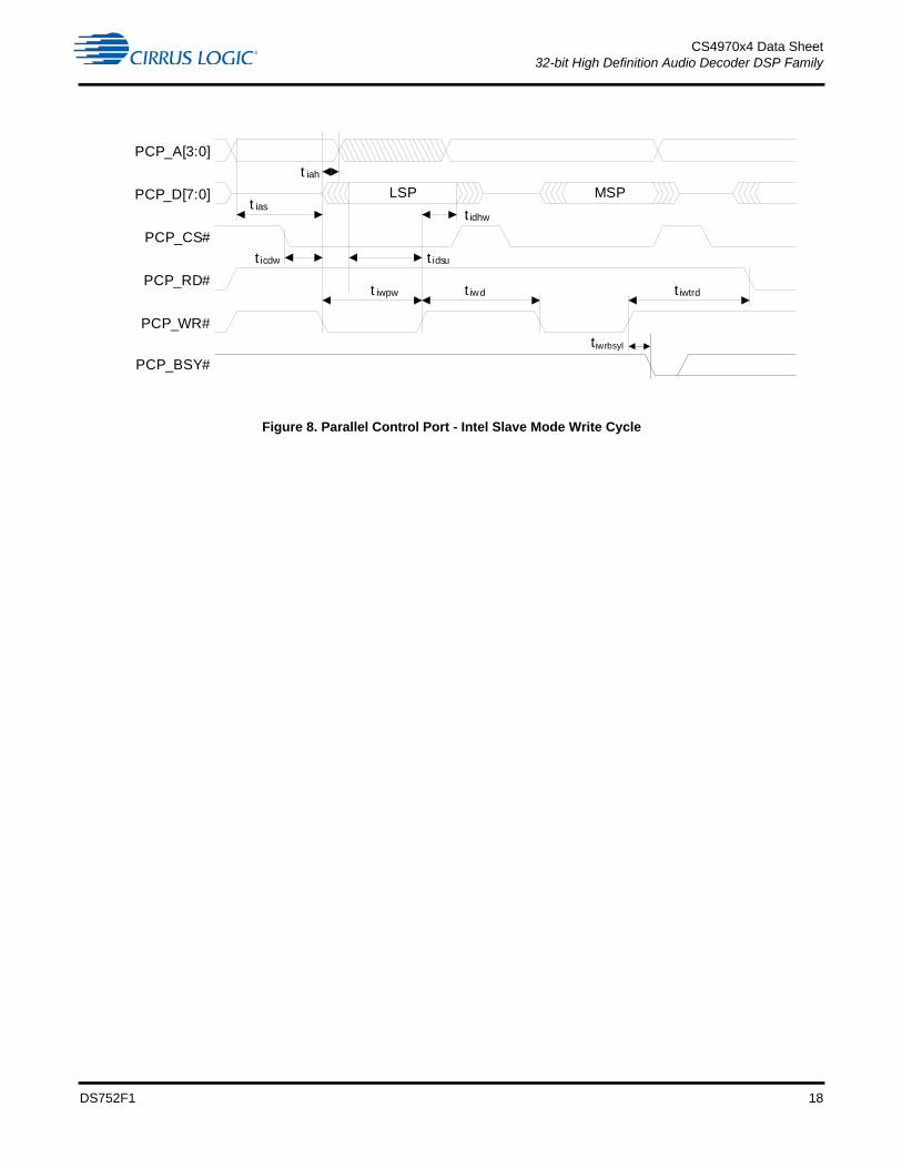
Delay between PCP_WR then PCP_CS low or PCP_CS then
PCP_WR low
ticdw 0 — — ns
Data setup before PCP_CS or PCP_WR high tidsu 8 — — ns
PCP_CS and PCP_WR low for write tiwpw 24 — — ns
Data hold after PCP_CS or PCP_WR high tidhw 8 — — ns
PCP_CS or PCP_WR high to PCP_CS and PCP_RD low for next
read1tiwtrd 30 — — ns
PCP_CS or PCP_WR high to PCP_CS and PCP_WR low for next
write1tiwd 30 — — ns
PCP_WR rising to PCP_BSY falling tiwrbsyl — 2*DCLKP + 20 — ns
1. The system designer should be aware that the actual maximum speed of the communication port may be limited by the firmware application. Hardware handshaking on the PCP_BSY pin/bit should be observed to prevent overflowing the input data buffer. CS4953x4/CS4970x4 System Designer’s Guide should be consulted for the firmware speed limitations.
Parameter Symbol Min Typical Max Unit
PCP_A[3:0]
PCP_D[7:0]t ias
t icdr
t iah
t idd
t irpw
t idhr
t idis
t ird t irdtw
PCP_CS#
PCP_WR#
PCP_RD#
PCP_IRQ#
tirdirqh
LSP MSP
DS752F1 17
CS4970x4 Data Sheet32-bit High Definition Audio Decoder DSP Family
Figure 8. Parallel Control Port - Intel Slave Mode Write Cycle
t ias
t icdw
t iah
t iwpw
t idhw
t iwd t iwtrd
t idsu
tiwrbsyl
PCP_D[7:0]
PCP_CS#
PCP_WR#
PCP_RD#
PCP_A[3:0]
PCP_BSY#
LSP MSP
DS752F1 18

CS4970x4 Data Sheet32-bit High Definition Audio Decoder DSP Family
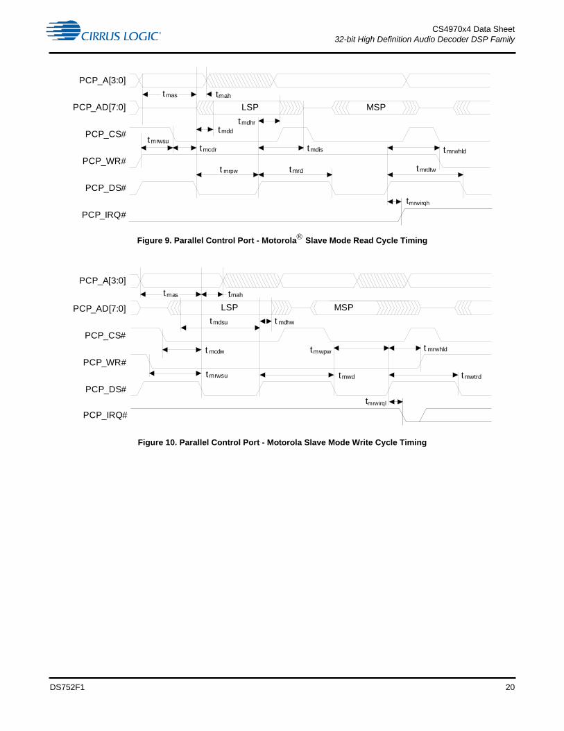
5.14 Switching Characteristics — Parallel Control Port - Motorola Slave Mode
ParameterSymbo
l Min Typical Max Unit
Address setup before PCP_CS and PCP_DS low tmas 5 — — ns
Address hold time after PCP_CS and PCP_DS low tmah 5 — — ns
Read
Delay between PCP_DS then PCP_CS low or PCP_CS then
PCP_DS low
tmcdr 0 — — ns
Data valid after PCP_CS and PCP_DS low with PCP_R/W high tmdd — — 19 ns
PCP_CS and PCP_DS low for read tmrpw 24 — — ns
Data hold time after PCP_CS or PCP_DS high after read tmdhr 8 — — ns
Data high-Z after PCP_CS or PCP_DS high after read tmdis — — 18 ns
PCP_CS or PCP_DS high to PCP_CS and PCP_DS low for next
read1
1. The system designer should be aware that the actual maximum speed of the communication port may be limited by the firmware application. Hardware handshaking on the PCP_BSY pin/bit should be observed to prevent overflowing the input data buffer. CS4953x4/CS4970x4 System Designer’s Guide should be consulted for the firmware speed limitations.
tmrd 30 — — ns
PCP_CS or PCP_DS high to PCP_CS and PCP_DS low for next
write1tmrdtw 30 — — ns
PCP_RW rising to PCP_IRQ falling tmrwirqh — — 12 ns
Write
Delay between PCP_DS then PCP_CS low or PCP_CS then
PCP_DS low
tmcdw 0 — — ns
Data setup before PCP_CS or PCP_DS high tmdsu 8 — — ns
PCP_CS and PCP_DS low for write tmwpw 24 — — ns
PCP_R/W setup before PCP_CS AND PCP_DS low tmrwsu 24 — — ns
PCP_R/W hold time after PCP_CS or PCP_DS high tmrwhld 8 — — ns
Data hold after PCP_CS or PCP_DS high tmdhw 8 — — ns
PCP_CS or PCP_DS high to PCP_CS and PCP_DS low with
PCP_R/W high for next read1tmwtrd 30 — — ns
PCP_CS or PCP_DS high to PCP_CS and PCP_DS low for next
write1tmwd 30 — — ns
PCP_RW rising to PCP_BSY falling tmrwbsyl — 2*DCLKP + 20 — ns
DS752F1 19
CS4970x4 Data Sheet32-bit High Definition Audio Decoder DSP Family
Figure 9. Parallel Control Port - Motorola Slave Mode Read Cycle Timing
Figure 10. Parallel Control Port - Motorola Slave Mode Write Cycle Timing
tmas
tmcdr
tmah
tmdd
t mrpw
tmdhr
tmdis
tmrd tmrdtw
tmrwsu
tmrwhld
PCP_A[3:0]
PCP_AD[7:0]
PCP_CS#
PCP_WR#
PCP_DS#
PCP_IRQ#
tmrwirqh
LSP MSP
tmas
tmdsu t mdhw
tmwd tmwtrd
tmwpwt mcdw
tmrwsu
t mrwhld
maht
PCP_A[3:0]
PCP_AD[7:0]
PCP_CS#
PCP_WR#
PCP_DS#
PCP_IRQ#
tmrwirql
LSP MSP
DS752F1 20
CS4970x4 Data Sheet32-bit High Definition Audio Decoder DSP Family
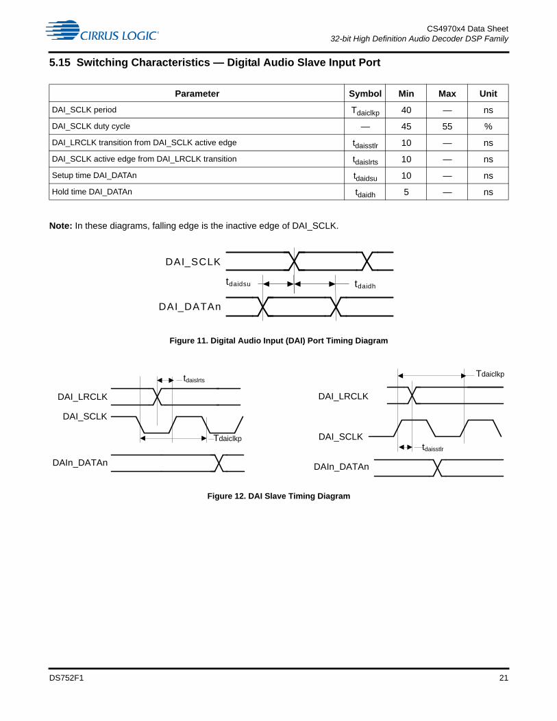
5.15 Switching Characteristics — Digital Audio Slave Input Port
Note: In these diagrams, falling edge is the inactive edge of DAI_SCLK.
Figure 11. Digital Audio Input (DAI) Port Timing Diagram
Figure 12. DAI Slave Timing Diagram
Parameter Symbol Min Max Unit
DAI_SCLK period Tdaiclkp 40 — ns
DAI_SCLK duty cycle — 45 55 %
DAI_LRCLK transition from DAI_SCLK active edge tdaisstlr 10 — ns
DAI_SCLK active edge from DAI_LRCLK transition tdaislrts 10 — ns
Setup time DAI_DATAn tdaidsu 10 — ns
Hold time DAI_DATAn tdaidh 5 — ns
DAI_SCLK
DAI_DATAn
tdaidhtdaidsu
DAI_SCLK
DAI_LRCLK
DAIn_DATAn
tdaislrts
Tdaiclkp DAI_SCLK
DAI_LRCLK
tdaisstlr
Tdaiclkp
DAIn_DATAn
DS752F1 21

CS4970x4 Data Sheet32-bit High Definition Audio Decoder DSP Family
5.16 Switching Characteristics — Digital Audio Output Port
Figure 13. Digital Audio Port Output Timing Master Mode
Parameter Symbol Min Max Unit
DAO_MCLK period Tdaomclk 40 — ns
DAO_MCLK duty cycle — 45 55 %
DAO_SCLK period for Master or Slave mode1
1. Master mode timing specifications are characterized, not production tested.
Tdaosclk 40 — ns
DAO_SCLK duty cycle for Master or Slave mode1 — 40 60 %
Master Mode (Output A1 Mode)1,2
2. Master mode is defined as the CS4970x4 driving both DAO_SCLK, DAO_LRCLK. When MCLK is an input, it is divided to produce DAO_SCLK, DAO_LRCLK.
DAO_SCLK delay from DAO_MCLK rising edge,
DAO_MCLK as an input
tdaomsck — 19 ns
DAO_SCLK delay from DAO_LRCLK transition3 tdaomlrts — 8 ns
DAO_LRCLK delay from DAO_SCLK transition3
3. This timing parameter is defined from the non-active edge of DAO_SCLK. The active edge of DAO_SCLK is the point at which the data is valid.
tdaomstlr — 8 ns
DAO1_DATA[3..0], DAO2_DATA[1..0]
delay from DAO_SCLK transition3tdaomdv — 10 ns
Slave Mode (Output A0 Mode)4
4. Slave mode is defined as DAO_SCLK, DAO_LRCLK driven by an external source.
DAO_SCLK active edge to DAO_LRCLK transition tdaosstlr 10 — ns
DAO_LRCLK transition to DAO_SCLK active edge tdaoslrts 10 — ns
DAO_Dx delay from DAO_SCLK inactive edge tdaosdv — 12.5 ns
DAO_MCLK
DAO_SCLK
DAO_LRCLK
DAOn_DATAn
tdaomlclk
tdaomsck
tdaomdv
tdaomlrts
DAO_MCLK
DAO_SCLK
DAO_LRCLK
DAOn_DATAn
tdaomlclk
tdaomsck
tdaomdv
tdaomlrts
Note: In these diagrams, falling edge is the inactive edge of DAO_SCLK.
DS752F1 22

CS4970x4 Data Sheet32-bit High Definition Audio Decoder DSP Family
Figure 14. Digital Audio Output Timing, Slave Mode (Relationship LRCLK to SCLK)
5.17 Switching Characteristics — SDRAM InterfaceRefer to Figure 15 through Figure 18.
(SD_CLKOUT = SD_CLKIN)
Parameter Symbol Min Typical Max Unit
SD_CLKIN high time tsdclkh 2.3 — — ns
SD_CLKIN low time tsdclkl 2.3 — — ns
SD_CLKOUT rise/fall time tsdclkrf — — 1 ns
SD_CLKOUT Frequency — — 150 — MHz
SD_CLKOUT duty cycle — 45 — 55 %
SD_CLKOUT rising edge to signal valid tsdcmdv — — 3.8 ns
Signal hold from SD_CLKOUT rising edge tsdcmdh — 1.1 — ns
SD_CLKOUT rising edge to SD_DQMn valid tsddqv — 3.8 — ns
SD_DQMn hold from SD_CLKOUT rising edge tsddqh 1.38 — — ns
SD_DATA valid setup to SD_CLKIN rising edge tsddsu 1.3 — — ns
SD_DATA valid hold to SD_CLKIN rising edge tsddh 2.1 — — ns
SD_CLKOUT rising edge to ADDRn valid tsdav — 3.8 — ns
DAO_SCLK
DAO_LRCLK
DAO_Dx
tdaoslrts
tdaosclk
DAO_SCLK
DAO_LRCLK
tdaosstlr tdaosdv
tdaosclk
DAO_Dx
Note: In these diagrams, Falling edge is the inactive edge of DAO_SCLK
DS752F1 23

D
CS
4970x4
Da
ta S
heet
32-bit Hig
h Definitio
n Audio
De
coder D
SP
Fam
ily
3 MSP3
11
S752F
12
4
Figure 15. External Memory Interface - SDRAM Burst Read Cycle
Figure 16. External Memory Interface - SDRAM Burst Write Cycle
SD_CLKOUT
SD_CS#
SD_RAS#
SD_CAS#
SD_WE#
SD_DQMn
SD_An
SD_Dn
tsddsu
tsdclkrftsdcmdv
tsdav
tsddqv
tsdcmdh
tsddh
tsddqh
CAS=2LSP0 MSP0 LSP
SD_CLKIN
tsdclkl tsdclkh
00
LSP1 MSP1 LSP2 MSP2
SD_CLKOUT
SD_CS#
SD_RAS#
SD_CAS#
SD_WE#
tsdcmdv tsdcmdh
SD_Dn LSP0 MSP0 LSP1 MSP1 LSP2 MSP2 LSP3 MSP3
SD_An
SD_DQMn
tsddqh
00 11
tsddqv
tsdav

CS4970x4 Data Sheet32-bit High Definition Audio Decoder DSP Family
Figure 17. External Memory Interface - SDRAM Auto Refresh Cycle
SD_CLKOUT
SD_CS#
SD_RAS#
SD_CAS#
SD_WE#
SD_DQMn
SD_An
SD_Dn
tsdcmdv tsdcmdhtsdcmdv
DS752F1 25

CS4970x4 Data Sheet32-bit High Definition Audio Decoder DSP Family
Figure 18. External Memory Interface - SDRAM Load Mode Register Cycle
SD_CLKOUT
SD_CS#
SD_RAS#
SD_CAS#
SD_WE#
SD_DQMn
SD_An
SD_Dn
OPCODE
tsdcmdv tsdcmdh
DS752F1 26

CS4970x4 Data Sheet32-bit High Definition Audio Decoder DSP Family
6 Ordering InformationThe CS4970x4 family part number is described as follows:
CS497NNI-XYZ
where
NN - Product Number Variant
I - ROM ID Number
X - Product Grade
Y - Package Type
Z - Lead (Pb) Free
Note: Please contact the factory for availability of the -D (automotive grade) package.
7 Environmental, Manufacturing, and Handling Information
* MSL (Moisture Sensitivity Level) as specified by IPC/JEDEC J-STD-020.
Table 4. Ordering Information
Part No. Status Grade Temp. Range Package
CS497014-CVZ Active Commercial 0 to +70 °C 128-pin LQFP
CS47014-CVZR1
1. R = Tape and reel
Active Commercial 0 to +70 °C
CS497024-CVZ Active Commercial 0 to +70 °C 128-pin LQFP
CS497024-CVZR1 Active Commercial 0 to +70 °C
Table 5. Environmental, Manufacturing, & Handling Information
Model Number Peak Reflow Temp MSL Rating* Max Floor Life
CS497014-CVZ 260 °C 3 7 Days
CS47014-CVZR 260 °C 3 7 Days
CS497024-CVZ 260 °C 3 7 Days
CS497024-CVZR 260 °C 3 7 Days
DS752F1 27
CS4970x4 Data Sheet32-bit High Definition Audio Decoder DSP Family
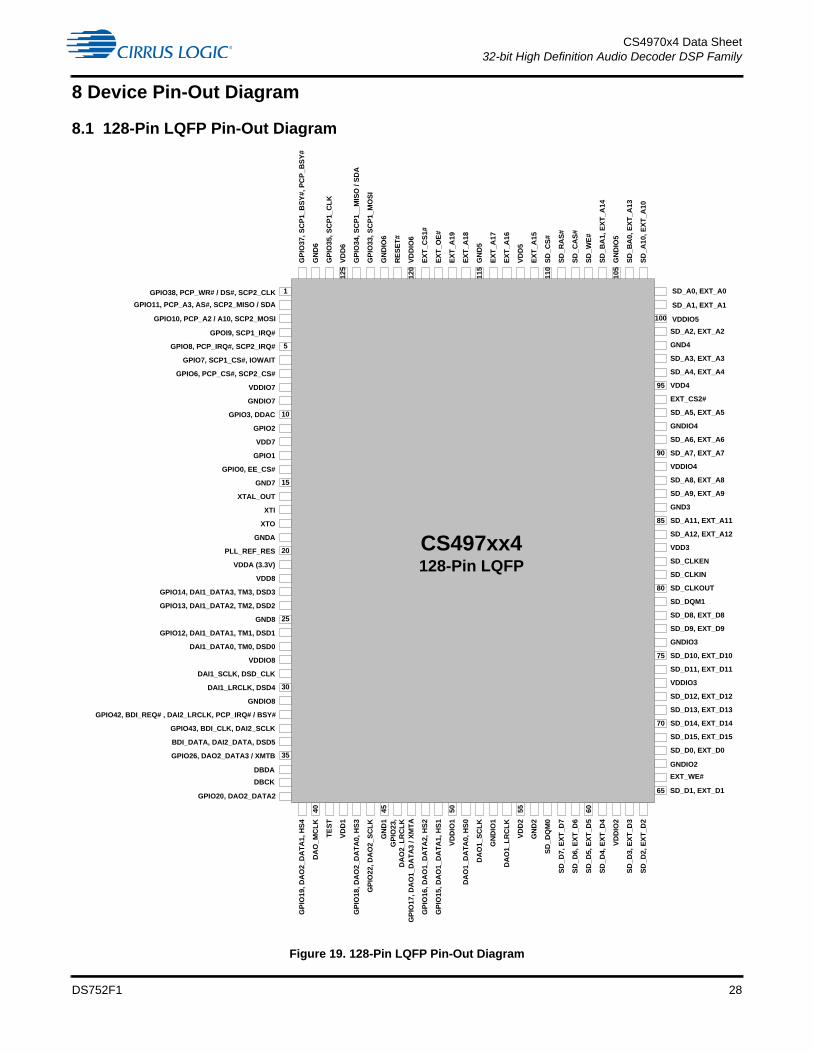
8 Device Pin-Out Diagram
8.1 128-Pin LQFP Pin-Out Diagram
Figure 19. 128-Pin LQFP Pin-Out Diagram
GPIO2
GPIO1
GPIO0, EE_CS#
XTO
VDD7
GND7
VDDIO7
XTI
GNDIO7
GNDA
PLL_REF_RES
VDDA (3.3V)
VDD8
GND8
GPIO13, DAI1_DATA2, TM2, DSD2
GPIO14, DAI1_DATA3, TM3, DSD3
DAI1_DATA0, TM0, DSD0
GPIO12, DAI1_DATA1, TM1, DSD1
GPIO6, PCP_CS#, SCP2_CS#
GPIO38, PCP_WR# / DS#, SCP2_CLK
VD
D6
GN
D6
GPIO10, PCP_A2 / A10, SCP2_MOSI
GPIO8, PCP_IRQ#, SCP2_IRQ#
GP
IO37
, SC
P1_
BS
Y#,
PC
P_B
SY
#
VD
DIO
6
GPIO11, PCP_A3, AS#, SCP2_MISO / SDA
GN
DIO
6
GPOI9, SCP1_IRQ#
GP
IO34
, SC
P1_
_MIS
O /
SD
A
GP
IO33
, SC
P1_
MO
SI
GP
IO35
, SC
P1_
CL
K
VD
D5
VDDIO5
GN
D5
GN
DIO
5
SD
_C
AS
#
SD
_R
AS
#
SD_A3, EXT_A3
SD_A2, EXT_A2
SD_A1, EXT_A1
SD_A0, EXT_A0
SD
_A
10, E
XT
_A10
SD_A11, EXT_A11
VDD4
GND4
SD
_C
S#
SD_A4, EXT_A4
SD_A5, EXT_A5
SD_A6, EXT_A6
SD_A7, EXT_A7
SD_A8, EXT_A8
SD_CLKEN
SD_A9, EXT_A9
VDDIO4
GNDIO4
SD_CLKOUT
SD_CLKIN
SD_D10, EXT_D10
SD_D11, EXT_D11
SD_D12, EXT_D12
VDD3
GND3
SD_D13, EXT_D13
SD_D14, EXT_D14
SD_D15, EXT_D15
SD_DQM1
SD
_D7,
EX
T_D
7
SD
_D6,
EX
T_D
6
VDDIO3
GNDIO3
SD
_D5,
EX
T_D
5
SD
_DQ
M0
SD
_D4,
EX
T_D
4
SD
_D3,
EX
T_D
3
SD
_D2,
EX
T_D
2
GP
IO1
7, D
AO
1_D
AT
A3
/ XM
TA
GP
IO15
, DA
O1_
DA
TA
1, H
S1
DA
O1_
DA
TA
0, H
S0
DA
O1_
LR
CL
K
DAI1_LRCLK, DSD4
DA
O_M
CL
K
GPIO20, DAO2_DATA2
DAI1_SCLK, DSD_CLK
VD
D1
GN
D1
DA
O1_
SC
LK
GP
IO16
, DA
O1_
DA
TA
2, H
S2
GP
IO23
, D
AO
2_L
RC
LK
R
ES
ET
#
VD
DIO
1
GP
IO22
, DA
O2_
SC
LK
GN
DIO
1
GP
IO18
, D
AO
2_D
AT
A0
, HS
3
GP
IO19
, D
AO
2_D
AT
A1
, HS
4
VD
D2
GN
D2
GPIO26, DAO2_DATA3 / XMTB
VD
DIO
2
GNDIO2
SD
_W
E#
SD_D0, EXT_D0
SD_D1, EXT_D1
SD_D8, EXT_D8
SD_D9, EXT_D9
SD_A12, EXT_A12
SD
_B
A1,
EX
T_A
14
SD
_B
A0,
EX
T_A
13
GPIO7, SCP1_CS#, IOWAIT
VDDIO8
GNDIO8
EX
T_A
15
EX
T_A
16
EX
T_A
17
EX
T_A
18
EX
T_A
19
EX
T_C
S1#
EX
T_O
E#
EXT_WE#
GPIO3, DDAC
TE
ST
DBDA
DBCK
XTAL_OUT
GPIO43, BDI_CLK, DAI2_SCLK
GPIO42, BDI_REQ# , DAI2_LRCLK, PCP_IRQ# / BSY#
BDI_DATA, DAI2_DATA, DSD5
EXT_CS2#
10
15
20
25
30
5
35
1
125
120
115
110
105
95
90
85
80
75
70
65
10040 45 50 55 60
CS497xx4128-Pin LQFP
DS752F1 28

CS4970x4 Data Sheet32-bit High Definition Audio Decoder DSP Family
9 Package Mechanical Drawings
9.1 128-Pin LQFP Package Drawing
Figure 20. 128-Pin LQFP Package Drawing
Table 6. 128-Pin LQFP Package Characteristics
DIM MILLIMETERS INCHES
MIN NOM MAX MIN NOM MAX
A — — 1.60 — — .063”
A1 0.05 — 0.15 .002” — .006”
b 0.17 0.22 0.27 .007” .009” .011”
D 22.00 BSC .866”
D1 20.00 BSC .787”
E 16.00 BSC .630”
E1 14.00 BSC .551”
e 0.50 BSC .020”
q 0° 3.5 7° 0° 3.5 7°
L 0.45 0.60 0.75 .018” .024” .030”
L1 1.00 REF .039” REF
TOLERANCES OF FORM AND POSITION
ddd 0.08 .003”
D1D
E1E
1
e
L
b
A1
A
DS752F1 29
CS4970x4 Data Sheet32-bit High Definition Audio Decoder DSP Family
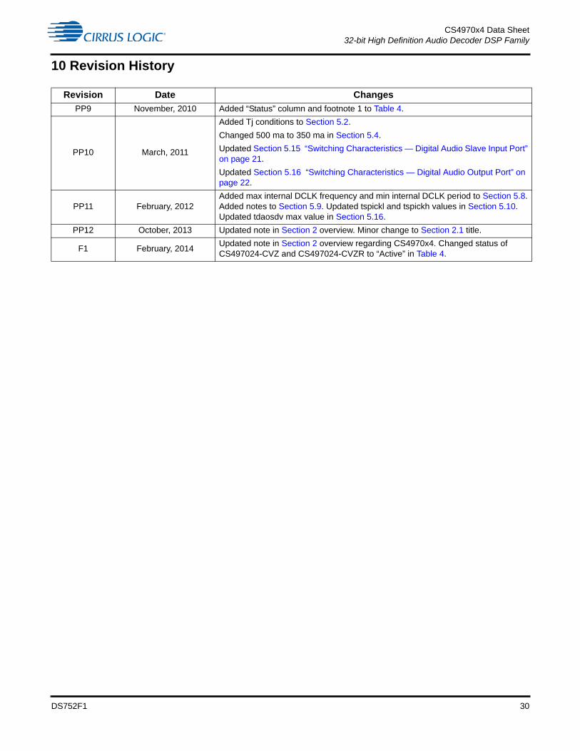
10 Revision History
Revision Date Changes
PP9 November, 2010 Added “Status” column and footnote 1 to Table 4.
PP10 March, 2011
Added Tj conditions to Section 5.2.
Changed 500 ma to 350 ma in Section 5.4.
Updated Section 5.15 “Switching Characteristics — Digital Audio Slave Input Port” on page 21.
Updated Section 5.16 “Switching Characteristics — Digital Audio Output Port” on page 22.
PP11 February, 2012Added max internal DCLK frequency and min internal DCLK period to Section 5.8. Added notes to Section 5.9. Updated tspickl and tspickh values in Section 5.10. Updated tdaosdv max value in Section 5.16.
PP12 October, 2013 Updated note in Section 2 overview. Minor change to Section 2.1 title.
F1 February, 2014Updated note in Section 2 overview regarding CS4970x4. Changed status of CS497024-CVZ and CS497024-CVZR to “Active” in Table 4.
DS752F1 30

CS4970x4 Data Sheet32-bit High Definition Audio Decoder DSP Family
Contacting Cirrus Logic Support For all product questions and inquiries, contact a Cirrus Logic Sales Representative. To find the one nearest you, go to www.cirrus.com.
IMPORTANT NOTICE
Cirrus Logic, Inc. and its subsidiaries (“Cirrus”) believe that the information contained in this document is accurate and reliable. However, the information is subject tochange without notice and is provided “AS IS” without warranty of any kind (express or implied). Customers are advised to obtain the latest version of relevantinformation to verify, before placing orders, that information being relied on is current and complete. All products are sold subject to the terms and conditions of salesupplied at the time of order acknowledgment, including those pertaining to warranty, indemnification, and limitation of liability. No responsibility is assumed by Cirrusfor the use of this information, including use of this information as the basis for manufacture or sale of any items, or for infringement of patents or other rights of thirdparties. This document is the property of Cirrus and by furnishing this information, Cirrus grants no license, express or implied under any patents, mask work rights,copyrights, trademarks, trade secrets or other intellectual property rights. Cirrus owns the copyrights associated with the information contained herein and givesconsent for copies to be made of the information only for use within your organization with respect to Cirrus integrated circuits or other products of Cirrus. This consentdoes not extend to other copying such as copying for general distribution, advertising or promotional purposes, or for creating any work for resale.
CERTAIN APPLICATIONS USING SEMICONDUCTOR PRODUCTS MAY INVOLVE POTENTIAL RISKS OF DEATH, PERSONAL INJURY, OR SEVEREPROPERTY OR ENVIRONMENTAL DAMAGE (“CRITICAL APPLICATIONS”). CIRRUS PRODUCTS ARE NOT DESIGNED, AUTHORIZED OR WARRANTED FORUSE IN PRODUCTS SURGICALLY IMPLANTED INTO THE BODY, AUTOMOTIVE SAFETY OR SECURITY DEVICES, LIFE SUPPORT PRODUCTS OR OTHERCRITICAL APPLICATIONS. INCLUSION OF CIRRUS PRODUCTS IN SUCH APPLICATIONS IS UNDERSTOOD TO BE FULLY AT THE CUSTOMER’S RISK ANDCIRRUS DISCLAIMS AND MAKES NO WARRANTY, EXPRESS, STATUTORY OR IMPLIED, INCLUDING THE IMPLIED WARRANTIES OF MERCHANTABILITYAND FITNESS FOR PARTICULAR PURPOSE, WITH REGARD TO ANY CIRRUS PRODUCT THAT IS USED IN SUCH A MANNER. IF THE CUSTOMER ORCUSTOMER’S CUSTOMER USES OR PERMITS THE USE OF CIRRUS PRODUCTS IN CRITICAL APPLICATIONS, CUSTOMER AGREES, BY SUCH USE, TOFULLY INDEMNIFY CIRRUS, ITS OFFICERS, DIRECTORS, EMPLOYEES, DISTRIBUTORS AND OTHER AGENTS FROM ANY AND ALL LIABILITY, INCLUDINGATTORNEYS’ FEES AND COSTS, THAT MAY RESULT FROM OR ARISE IN CONNECTION WITH THESE USES.
Cirrus Logic, Cirrus, Cirrus Logic logo designs, Cirrus Framework, and DSP Condenser are trademarks of Cirrus Logic, Inc. All other brand and product names in thisdocument may be trademarks or service marks of their respective owners.
THX is a registered trademark of THX, Ltd. THX Select 2 and THX Ultra 2 are trademarks of THX, Ltd.
Dolby, Dolby Digital, Dolby Headphone, Virtual Speaker, Pro Logic, Audistry, and Dolby Volume are registered trademarks of Dolby Laboratories, Inc. AAC, AC-3,Dolby TrueHD, and Dolby Volume 258 are trademarks of Dolby Laboratories, Inc. Supply of an implementation of Dolby Technology does not convey a license norimply a right under any patent, or any other industrial or Intellectual Property Right of Dolby Laboratories, to use the Implementation in any finished end-user or ready-to-use final product. It is hereby notified that a license for such use is required from Dolby Laboratories.
DTS and DTS Neo:6 are registered trademarks of the Digital Theater Systems, Inc. DTS-ES 96/24, DTS-ES, DTS 6.1, DTS 96/24, DTS Neural Surround, and DTSExpress are trademarks of Digital Theater Systems, Inc. It is hereby notified that a third-party license from DTS is necessary to distribute software of DTS in anyfinished end-user or ready-to-use final product.
SRS, SRS 3D, SRS CS Auto, SRS CS Headphone, SRS Circle Cinema 3D, SRS Circle Surround, SRS Circle Surround II, SRS GEQ, SRS Hardlimiter, SRSHeadphone, SRS Headphone 360, SRS HPF, SRS StudioSound HD, SRS TruEQ, SRS TruMedia, SRS TruSurround, SRS TruSurround XT, SRS TruSurround HD,SRS TruSurround HD4, SRS TruVolume, SRS VIP+, SRS WOW, SRS WOW XT, SRS WOW HD are either trademarks or registered trademarks of SRS Labs, Inc.SRS, SRS 3D, SRS CS Auto, SRS CS Headphone, SRS Circle Cinema 3D, SRS Circle Surround, SRS Circle Surround II, SRS GEQ, SRS Hardlimiter, SRSHeadphone, SRS Headphone 360, SRS HPF, SRS StudioSound HD, SRS TruEQ, SRS TruMedia, SRS TruSurround, SRS TruSurround XT, SRS TruSurround HD,SRS TruSurround HD4, SRS TruVolume, SRS VIP+, SRS WOW, SRS WOW XT, SRS WOW HD technologies are incorporated under license from SRS Labs, Inc.SRS, SRS 3D, SRS CS Auto, SRS CS Headphone, SRS Circle Cinema 3D, SRS Circle Surround, SRS Circle Surround II, SRS GEQ, SRS Hardlimiter, SRSHeadphone, SRS Headphone 360, SRS HPF, SRS StudioSound HD, SRS TruEQ, SRS TruMedia, SRS TruSurround, SRS TruSurround XT, SRS TruSurround HD,SRS TruSurround HD4, SRS TruVolume, SRS VIP+, SRS WOW, SRS WOW XT, SRS WOW HD technologies incorporated in the Cirrus Logic CS4953xx productsare owned by SRS Labs, a U.S. Corporation and licensed to Cirrus Logic, Inc. Purchaser of Cirrus Logic CS4953xx products must sign a license for use of the chipand display of the SRS Labs trademarks. Any products incorporating the Cirrus Logic CS4953xx products must be sent to SRS Labs for review. SRS, SRS 3D, SRSCS Auto, SRS CS Headphone, SRS Circle Cinema 3D, SRS Circle Surround, SRS Circle Surround II, SRS GEQ, SRS Hardlimiter, SRS Headphone, SRS Headphone360, SRS HPF, SRS Studio-Sound HD, SRS TruEQ, SRS TruMedia, SRS TruSurround, SRS TruSurround XT, SRS TruSurround HD, SRS TruSurround HD4, SRSTruVolume, SRS VIP+, SRS WOW, SRS WOW XT, SRS WOW HD technologies are protected under US and foreign patents issued and/or pending. Neither thepurchase of the Cirrus Logic CS4953xx products, nor the corresponding sale of audio enhancement equipment conveys the right to sell commercialized recordingsmade with any SRS technology/solution. SRS Labs requires all set makers to comply with all rules and regulations as outlined in the SRS Trademark Usage Manual.
Motorola is a registered trademark of Motorola, Inc. SPI is a trademark of Motorola, Inc.
Intel is a registered trademark of Intel Corporation.
I2C is a trademark of Philips Semiconductor.
DS752F1 31