organic molecular beam deposition: fundamentals, growth ... · organic molecular beam deposition:...
TRANSCRIPT
1
Organic Molecular Beam Deposition:
Fundamentals, Growth Dynamics, and In-Situ Studies S. Kowarik, A. Gerlach, F. Schreiber
Institut für Angewandte Physik, Universität Tübingen, Auf der Morgenstelle 10,
72076 Tübingen, Germany
We review recent progress on thin film growth by organic molecular beam deposition
(OMBD). We give a brief overview of growth physics with emphasis on the specific
characteristics of organic materials, such as weak van-der-Waals binding forces and
conformational and orientational degrees of freedom of the molecular building blocks. Two
recent developments in experimental studies of OMBD will be discussed in more detail:
(1) we will give examples for real-time and in-situ growth studies during deposition of the
organic semiconductors pentacene, diindenoperylene, and PTCDA and (2) we will give an
overview of high precision in-situ investigations of the first molecular monolayer, in
particular using the x-ray standing wave technique.

2
I. Introduction
The strong increase in research activity on organic thin films is to a large extent, although not
exclusively, motivated by the perspectives of and in some cases already realised applications
in various areas including electronics and optoelectronics. Some examples for these are
included also in other reviews in this Special Issue [1]. At the same time, it has also been
recognised that the performance of devices is intimately coupled to the structural
characteristics. The understanding of growth is therefore mandatory to improve and control
devices.
In this review we focus on organic molecular beam deposition (OMBD), i.e. evaporation of
the molecules, usually in ultra-high vacuum (UHV). OMBD is the typical method of thin film
preparation for small molecule organic semiconductors because they often exhibit only low
solubility, while growth from solution (e.g. spin coating, inkjet printing, and spray coating)
enjoys great popularity in particular for polymeric systems. We should note that there is also
the term organic molecular beam epitaxy (OMBE) [2], but we consider OMBD as the more
general term, since it also includes systems without epitaxial relation to the substrate. From a
fundamental perspective, it has been realised that OMBD exhibits its own specifics different
from growth of atomic systems, e.g. changes of molecular conformation during growth [3],
large thermal expansion coefficients [4] or an additional source of disorder due to molecular
tilt domains [5]. The orientational / tilt degrees of freedom of molecules probably are the most
important difference to atomic systems, and imply that the problem is generally anisotropic,
and that not only the positional adsorption state of a molecule, but also its orientation must be
considered [6; 7].
The present review is concerned with some general aspects of OMBD and also a few recent
results. We will discuss
• typical systems
• general principles of growth
• specific characteristics of organics
• some examples / brief overview of growth behaviour
We will focus in particular on two recent developments, namely
(i) real-time studies of organic thin film growth, an important development to reveal transient
structures, that can modify the growth behaviour, and
(ii) high-resolution studies of the molecular adsorption geometry, which not only influences
the growth of the subsequent layers, but also has a strong impact on the charge carrier

3
(electron or hole) injection from metallic contacts into organic semiconductors, which can
easily be seen from the dependence of injection on distance and also from the (possibly
induced) interface dipole upon adsorption (possibly enhanced by molecular bending) [1; 8-
10].
In a review with limited space such as the present one, we of course cannot give an exhaustive
overview for which we refer to earlier reviews [11-17]. Instead, the examples are centred
mostly on our own work, which we will discuss in a broader context.
II. Some general considerations of growth Growth of crystalline thin films is an enormously rich subject with many different facets and
theoretical approaches, e.g. equilibrium considerations about crystal phases and shapes,
statistical analysis of correlation lengths and surface roughness, or detailed analysis of
dynamic processes of growth like diffusion and nucleation (see Figure 1). A thorough
treatment of its theoretical aspects can be found in References [18-21]. Here we want to
briefly touch the aspects of the in-plane crystallographic relationship, the out-of-plane
structure / evolution of morphology, as well as dynamic scaling before discussing specific
issues of organic thin film growth.
It is important to realise that a description of these aspects cannot solely rely on
thermodynamic arguments (by which we mean static, equilibrium considerations), but also
kinetic aspects of OMBD and its irreversible atomic scale processes (see Figure 1) must be
taken into account [22-25]. The growth of organic molecular films in particular often leads to
non-equilibrium structures due to the growth kinetics as can be seen from significant post-
growth re-organisation [26-28].
Absorption Re-desorption
intra-layer diffusion:
Nucleation / Dissociation
Interlayerdiffusion
Flux F [molecules/ s�cm2]
Figure 1 Schematic of atomistic processes relevant for OMBD.

4
1. Epitaxy / in-plane crystallographic relationship
We will not discuss in great detail the issues related to epitaxial relations, that is the
crystallographic relation between film and substrate, as some of our examples deal with
relaxed polycrystalline growth on amorphous substrates. For growth on crystalline substrates,
we want to point out that the strain induced by the lattice mismatch at the film substrate
interface is not only important in a crystallographic sense [2], but also influences the growth
beyond the structure of the first monolayer. For example it has been shown that
diindenoperylene (DIP) grown on NaCl single crystals exhibits herringbone type packing, but
when DIP is grown on crystalline perylene thin films an unusual sandwich herringbone type
packing is observed [29]. This suggests, that by careful selection of the (organic) substrate the
crystal structure of epitaxial adlayers can be controlled not only in the first monolayer
adjacent to the substrate, but also in following monolayers. In this respect the first monolayer
is the most important one, determining the crystal structure of an entire multilayer film. For
details on organic epitaxy see the review by Hooks et al. [30].
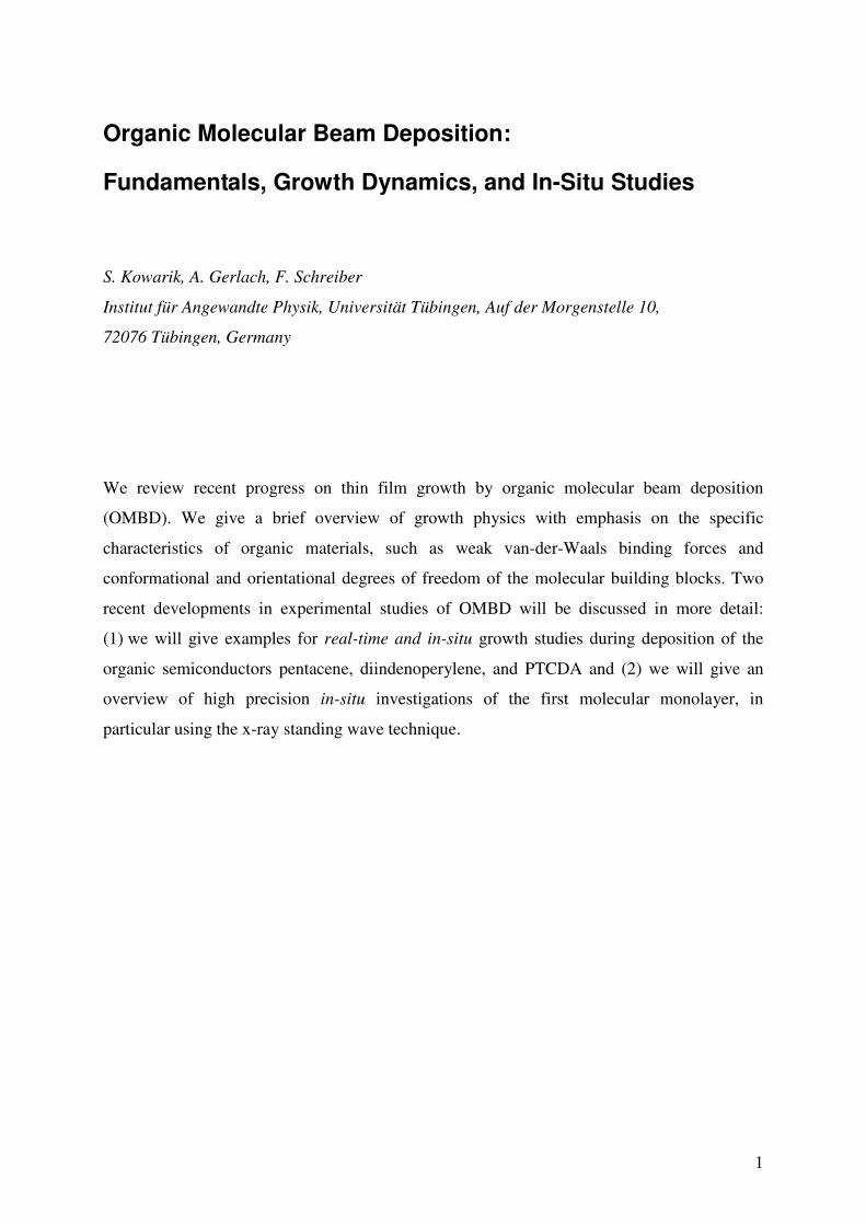
2. Overall structure (out of plane) / evolution of morphology
In general one can distinguish the three growth scenarios depicted in Figure 2: island
(Volmer-Weber), layer-plus-islands (Stranski-Krastanov), and layer-by-layer growth (Frank-
van-der-Merwe). Typically, the surface energies �substrate , �film, and �interface (see Figure 2) are
related to these growth modes using energetic (equilibrium) arguments.
Note that the modification of the substrate surface energy to change the growth behaviour of
the OMBD film has enjoyed some popularity. The most important strategy is based on the use
of self-assembled monolayers [13; 31]. Early work demonstrated the use of alkanethiol SAMs
on Au(111) to modify PTCDA growth [31-33]. In the context of pentacene growth this
strategy has been very successful [34-37], although it is not always obvious which feature of
the SAM exactly leads to the modification of the growth of the subsequent film. A detailed
discussion of this approach, however, is beyond the scope of this review.
In particular the layer-plus-island growth mode is typical for organic systems, as exemplified
by PTCDA on Ag(111) in this review. The examples of real-time growth studies in Section III
demonstrate that by measuring the out of plane morphology during growth one can readily
distinguish growth modes as well as measure threshold thicknesses where the growth
behaviour changes.
For a more detailed description in a given growth scenario, one must use an additional growth
model to quantify properties such as island size or film roughness and their evolution with
5
film thickness. For island growth that leads to roughening of the film surface, rate equation
models encompassing microscopic processes like interlayer diffusion (see Figure 1) can be
used [38]. In cases with little knowledge of atomic processes, the roughness evolution can be
more generally expressed in terms of growth exponents as discussed in the next section [39;
40].
� substrate� interface
� film
� film + � interface < � substrate
Surface energy contributions:
Growth modes:
� film + � interface > � substrate
island growth layer plus island growth layer-by-layer growth
Figure 2 Scenarios for thin film growth: Depending on the material specific surface free energies three
different generic growth modes are generally distinguished: island growth, layer plus island growth, and layer-
by-layer growth
3. Dynamic scaling
An important concept for the theoretical description of growth is based on dynamic scaling
[39-41]. During the last two decades a theoretical framework for relating growth mechanisms
to a set of scaling exponents has been developed, and there have been significant efforts to
theoretically predict and experimentally determine scaling exponents for certain growth
modes.
The film morphology can be described by scaling theory using three parameters for the
typical surface slope a, the correlation length � beyond which the heights at two points

6
become uncorrelated, and the standard deviation of the film height � (rms roughness)*. These
parameters scale with film thickness D according to a ~ D�, � ~ D1/z, � ~ D� , defining the
steepening exponent �, the dynamic exponent z, and the growth exponent �.
For organics, there are only few studies available. Interestingly, both DIP on siliconoxide as
well as phthalocyanines [42] seem to display significant roughening parameters (high �).
Values of the roughening parameter � > 0.5 indicate rapid roughening faster as expected for
random deposition in a ‘hit-and-stick’ model. Rapid roughening has been measured for DIP /
SiO2 (� = 0.748 ± 0.05), H2Pc / glass (� = 1.02 ± 0.08), and plasma polymer (� = 0.7 ± 0.10)
[42], but the effect is also found in inorganic materials [43].
4. Issues specific for growth of organic molecular materials
The general considerations above apply both to organic and inorganic materials, but several
aspects specific to organic materials can lead to distinctively different growth behaviour.
i) As extended objects, organic molecules have internal degrees of freedom. The
vibrational degrees of freedom can impact the interaction with the substrate and also
the thermalisation upon adsorption on the surface, because the translational energy of
a molecule can also be converted to internal vibrational energy. Conformational
degrees of freedom mean that the building block can change within the film, for
example by bending to accommodate stress. The conformation of the organic
semiconductor rubrene has been found to change during growth [3], which may
influence the film morphology [44]. Orientational degrees of freedom which are not
included in conventional growth models can give rise to tilt domains and thereby an
additional source of disorder, or may even give rise to ‘lying-down’ and ‘standing-up’
structures [6; 35] as discussed later for the example of DIP.
* The parameters are defined using the height difference correlation function (HDCF)
[ ]2( ) ( , ) ( ', ')g R h x y h x y= −
of two points laterally separated by 2 2( ') ( ')R x x y y= − + − . The
HDCF displays distinct behaviours for R << � and R >> �, where � denotes a correlation length. For R << � one expects a power law increase as g(R) � a2R2�, where � is the static roughness exponent and the prefactor a is a measure of the typical surface slope. For R >> x the heights at distance R become uncorrelated. Hence g(R) saturates at the value g(R) =2�2 , where 2( )h hσ = − is the standard deviation of the film height (or ‘rms roughness’).

7
ii) The interaction between molecules and between molecules and the substrate is often
dominated by weak van-der-Waals forces. It is important to emphasize that when
integrated over all atoms within a molecule, the weak interaction energies add up and
lead to substantial molecula binding energies in the eV. Nevertheless the weaker
interactions per atom lead to ‘softer’ materials and, for example, strain can be
accommodated more easily. Due to the weaker interactions the thermal expansion
coefficients (typically in the 10-4 1/K range) are large when compared to inorganic
materials, which possibly leads to higher thermally induced strain at film – substrate
interfaces.
iii) The size of the molecules and consequently the size of the unit cell is larger than that
of inorganic materials, and therefore the interaction potential is spread out over a
larger area. This weakens the effective substrate corrugation as experienced by
molecules because the small length scale substrate corrugation is averaged to some
extent over the size of the molecule which in general has inter-atomic bond lengths
different from the substrate. Also more translational and orientational domains for
epitaxy on inorganic substrates are possible due to the difference in unit cell size. This
introduces an additional source of disorder for organics.
III. Real-time and in-situ growth studies
With this review we build on previous reviews [11-17] and therefore will focus on recent
work on real-time and in-situ growth studies. In-situ techniques for monitoring organic
molecular beam deposition offer great advantages because post-growth sample changes such
as oxidation or de-wetting do not obscure the results, and, given a time resolution matching
the growth processes they also allow one to follow details of growth in real-time during the
deposition process. There exist a number of surface sensitive in-situ techniques with real-time
capability such as low-energy electron microscopy [45], reflection high-energy electron
diffraction (RHEED) [46], or helium scattering [47; 48]. Here we focus on x-ray scattering,
which offers flexibility in sample environment (vacuum / air / liquids / penetration of thin
solids), offers high spatial resolution and can be analyzed in most cases by a simple single
scattering (kinematic) theory.
8
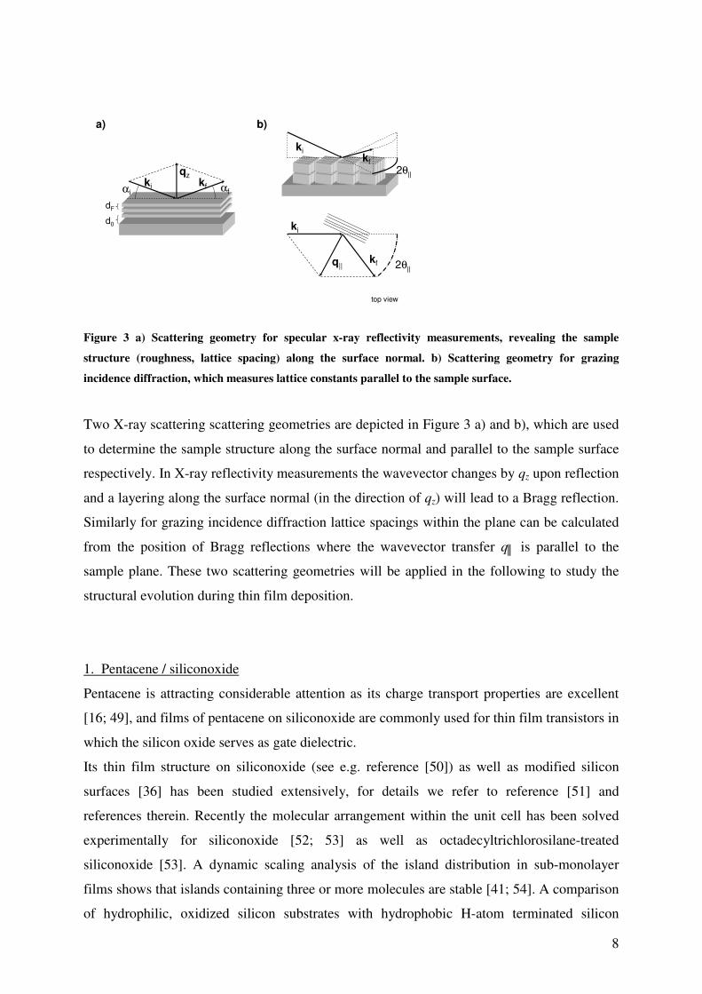
αi αf
qzki kf
2θ||
kikf
a) b)
dF
d0
2θ||
ki
kfq||
top view
Figure 3 a) Scattering geometry for specular x-ray reflectivity measurements, revealing the sample
structure (roughness, lattice spacing) along the surface normal. b) Scattering geometry for grazing
incidence diffraction, which measures lattice constants parallel to the sample surface.
Two X-ray scattering scattering geometries are depicted in Figure 3 a) and b), which are used
to determine the sample structure along the surface normal and parallel to the sample surface
respectively. In X-ray reflectivity measurements the wavevector changes by qz upon reflection
and a layering along the surface normal (in the direction of qz) will lead to a Bragg reflection.
Similarly for grazing incidence diffraction lattice spacings within the plane can be calculated
from the position of Bragg reflections where the wavevector transfer q� is parallel to the
sample plane. These two scattering geometries will be applied in the following to study the
structural evolution during thin film deposition.
1. Pentacene / siliconoxide
Pentacene is attracting considerable attention as its charge transport properties are excellent
[16; 49], and films of pentacene on siliconoxide are commonly used for thin film transistors in
which the silicon oxide serves as gate dielectric.
Its thin film structure on siliconoxide (see e.g. reference [50]) as well as modified silicon
surfaces [36] has been studied extensively, for details we refer to reference [51] and
references therein. Recently the molecular arrangement within the unit cell has been solved
experimentally for siliconoxide [52; 53] as well as octadecyltrichlorosilane-treated
siliconoxide [53]. A dynamic scaling analysis of the island distribution in sub-monolayer
films shows that islands containing three or more molecules are stable [41; 54]. A comparison
of hydrophilic, oxidized silicon substrates with hydrophobic H-atom terminated silicon

9
substrates has shown that with increasing hydrophobicity the nucleation density of pentacene
islands decreases by a factor of 100 while the island size increases [36]. Under optimized
conditions the island size in pentacene thin films can be as large as 0.1 mm as demonstrated in
Reference [45]. In addition to varying substrate temperature and deposition rate, the kinetic
energy of pentacene molecules has been varied in supersonic beam deposition [34; 47; 55].
Increasing the kinetic energy of pentacene molecules from 1.5 eV to 6.7 eV the adsorption
probability decreases by a factor of ~ 5, indicative of trapping-mediated adsorption [55].
0 2 4 6 8 10 12 14 160
1
2
Ref
lect
ivity
[a. u
.]
Time / Film Thickness [monolayers]
pentacene C22H14
layer-by-layer growth roughening
4 mono-layers
0
10
20
30
40
50
0.4
0.6
0.8
0.01
0.1
1
10
q [Å -1]
Ref
lect
ivity
[a. u
.]
Tim
e [m
in.]
first order Bragg reflection
second order Bragg reflection
0 1 2 3 4 5 6 7 8 9 100
5
10
15
20
25
0 1 2 3 4 5 6 7 8 9 100.0
0.2
0.4
0.6
0.8
1.0
Inte
rfac
e w
idth
[Å]
Thickness [Monolayers]
Laye
r cov
erag
e
a)
b)
c)
d)
e)
q = ¾ qBragg
Figure 4 a) Schematic of the pentacene molecule. b) Real-time measurements of the X-ray reflectivity in a
wide q-range during pentacene deposition on siliconoxide have been performed at the EDR beamline at
BESSY II (deposition rate 3.5 Å/min, substrate temperature 50 °C). Two peaks corresponding to the first
and second order Bragg reflection of the pentacene thin film phase can be seen to grow with increasing
deposition time (from Reference [59] with permission). c) Example of a growth oscillation at q = ¾ qBragg as
a cut through the data-set in (b), as indicated by the arrows. d) Using a diffusive growth model and the
kinematic approximation in X-ray scattering (see text) the interface roughness of the pentacene film and
the coverage of individual layers during growth can be extracted from the data-set in (b). e) From the
evolution of the surface roughness it can be seen that layer-by-layer growth persists for the first four
monolayers before roughening sets in.
10
Using real-time techniques, the evolution of different pentacene phases during growth [56],
dendritic island shape [45], the coverages of individual layers [57-59], or the Ehrlich-
Schwoebel barrier [58] can be studied. Real-time measurements of the X-ray reflectivity (as
shown in Figure 4 b), allow one to determine the crystal structure(s) from the positions of the
Bragg reflections, and also the evolution of the interface width (roughness) of the film can be
extracted. In Reference [56] it was shown that the nucleation of a second pentacene phase [50;
51; 60] occurs as early as the first pentacene monolayer as determined from following the
Bragg reflections corresponding to the two phases.
From the data in Figure 4 as well as grazing incidence diffraction data [59], it can be seen that
only the so called thin film phase of pentacene with an out-of-plane lattice constant of 15.6 Å
is growing for the conditions employed, as opposed to the pentacene bulk phase with a lattice
constant of 14.5 Å [51]. Analyzing not only the Bragg reflections, but also the evolution of
the reflectivity between the Bragg reflections, additional information can be learned. Halfway
between the Bragg reflections at the so called anti-Bragg point the interference of X-rays
scattered from neighbouring layers interferes destructively, leading to an oscillating X-ray
reflectivity when subsequent pentacene layers are filled. From these oscillations the number
of pentacene monolayers that have been grown can be directly counted (oscillation period two
monolayers). As can be seen from Figure 4 the X-ray reflectivity shows modulations not only
at the anti-Bragg condition, but also at all q-values other than the Bragg condition. These
growth oscillations at several q-points correspond to several Fourier components of the real-
space structure and therefore it is advantageous to measure the reflectivity in a wide q-space
region (0.25 - 0.8 Å-1 in this case) to get a precise measurement of the real-space structure
and the film roughness [61]. The growth oscillations can be described theoretically by the
following Equation (1), which includes the scattering from the substrate as well as the sum
over the scattering of every individual pentacene layer:
0
2( , )( , ) ( ) ( ) ( ) .Fi q d i n q d
reflected substrate nn
I q t A q e f q t eθΦ ⋅ ⋅ ⋅= ⋅ + ⋅ ⋅� (1)
Asubstrate(q): substrate scattering amplitude
f(q): molecular form factor of pentacene
�(q,d0): phase between substrate and ad-layer scattering
n: layer number;
�n: fractional coverage of the nth- layer (0 - zero coverage, 1 - filled layer);
q: X-ray wavevector transfer upon reflection;
dF: lattice spacing within the crystalline thin film;
11
To describe the time evolution of n(t) in equation (1) a range of growth models can be used
[19; 62; 63]. A simple model that can describe the experimental growth oscillations is a
diffusive growth model (Equation (2), see reference [62]) where the rate for a jump from layer
n+1 to n is proportional to the uncovered fraction of layer n+1 (i.e. how many molecules in
layer n+1 are not buried and free to move) and the available space in layer n (i.e. uncovered
space on top of layer n-1):
( ) 1 1 2 1 2 1 1( ) ( )( ) ( )( ).nn n n n n n n n n n n n
dk k
td
θ θ θ θ θ θ θ θ θ θ θτ
− + + − − − += − + − − − − − (2)
�n: fractional coverage of the nth- layer;
�: completion time for one monolayer
kn: effective rate for interlayer transport
Using equation (2) to calculate the n(t) and inserting them in equation (1) yields theoretical
growth oscillations which can be made to fit experimental values by adjusting the rate
constants kn. The solutions n(t) of equation (2) are S-shaped curves as shown in Figure 4 d).
The n(t) contain the complete information about the out-of-plane film structure, and as a
measure of the film roughness the interface width can be derived from them. The film
roughness or interface width is defined as the standard deviation of the interface from the
average film thickness:
_ _ _2 2 2
1 1 2 2 3interface width (1 ) (0 ) ( ) (1 ) ( ) (3 ) ...d d dθ θ θ θ θ= − ⋅ − + − ⋅ − + − ⋅ − + (3)
interface width: in units of the step height of one monolayer _
d : average film thickness units of the step height of one monolayer;
For pentacene, the roughness data shows a clear change in growth mode after four
monolayers. While the growth oscillations in the beginning show that pentacene grows in a
layer-by-layer fashion (with an oscillating surface roughness), after four monolayers the
surface width starts to increase. This change in growth mode from layer-by-layer growth to
roughening has also been observed in References [57; 58], where the interlayer transport of
pentacene molecules could be quantified. While the exact nature of this transition is unknown,
several factors may contribute such as decreased interlayer transport (increasing Schwoebel
barrier), faster nucleation, and decreased diffusivity on top of islands.

12
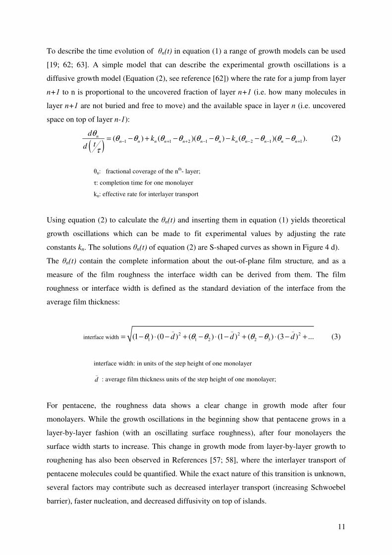
2. DIP / silicon oxide
Diindeno(1,2,3,-cd,10,20,30-lm)perylene (C32H16, DIP, a red dye, Figure 5 a) is less popular
than pentacene, but its growth has been studied in considerable detail. DIP has been shown to
exhibit excellent out of plane order [5; 64; 65] and also has been found to have promising
charge carrier mobility [49; 66].
Real-time measurements of the X-ray reflectivity for DIP in a wide q-range show the
appearance of the first and second order Bragg reflections of DIP ( Figure 5 b), evidencing the
growth of a DIP structure in which the individual molecules are ‘standing upright’.
Pronounced side maxima can be seen next to the DIP Bragg reflections (so called Laue
fringes), which originate from interference of reflections from the top and bottom surface of
the DIP film. The pronounced Laue fringes show that the DIP film surface remains smooth
during growth, and consequently growth oscillations are only weakly damped (Figure 5 c).
Modelling these growth oscillations again with the kinematic approximation of X-ray
scattering and a diffusive growth model (Equations (1) and(2)) yields the interface width
(roughness) and the individual layer coverages as in the pentacene case. By comparing Figure
4 b) and Figure 5 b), it is evident that for DIP the growth oscillations and Laue fringes are less
damped and the quantitative analysis in Figure 5 d) shows that DIP layer by layer growth
persists longer than in pentacene (up to ~7-8 monolayers as compared to 4 monolayers). Also
the absolute roughness is significantly lower than that of pentacene. After ~7 monolayers
roughening sets in for DIP as well, and indeed for thicker films the roughness increases faster
than expected for random deposition of molecules. This rapid roughening has been followed
to large film thicknesses of 10000 Å in Reference [5] and has also been found in other organic
systems [42].
13
a)
b)
diindenoperylene C32H16
020
4060
80100
120140
160180
200
0.20.3
0.40.5
0.60.7
0.8
10-310-210-1
100
101
q[Å -1]
Ref
lect
ivity
[a. u
.]
Tim
e [m
in.]
0 5 100.0
0.2
0.4
0.6
0.8
1.0
0 5 100
5
10
15
20
25
Thickness [Monolayers]
Laye
r cov
erag
e
Inte
rface
wid
th [Å
]
c)
d)
0 50 100 1500
5
10
15
200
2
4
6
80
20
40
60
Time [min.]
Ref
lect
ivity
[a. u
.]
q = ¾ qBragg
q = ½ qBragg
q = qBragg
Figure 5 a) Schematic of the diindenoperylene (DIP) molecule. b) Real-time measurements of the X-ray
reflectivity in a wide q-range during DIP deposition on siliconoxide have been performed at beamline
ID10B at the ESRF (deposition rate 0.6 Å/min, substrate temperature 130 °C). Two peaks corresponding
to the first and second order Bragg reflection of DIP can be seen to grow with increasing deposition time.
c) Cuts through the data-set in (b) show an oscillating X-ray reflectivity at the anti-Bragg condition and
the ¾ Bragg condition, while at the Bragg condition the reflectivity increases monotonically. Using a
diffusive growth model and the kinematic approximation in X-ray scattering (see text) the growth
oscillations can be fitted (solid line). d) From the fit of the growth oscillations the interface roughness of
the DIP film and the coverage of individual layers during growth can be extracted. It can be seen that
layer-by-layer growth persists for the first ~7 DIP monolayers before roughening sets in.
The reasons for the transition from layer-by-layer growth to roughening are not yet well
understood for complex organic molecular materials. Strained growth in the first monolayers
and strain relaxation may trigger a change in growth mode, but for organic molecules the
molecular tilt angle and the molecular conformation may also change during growth.
Differently tilted molecules will have different bulk- and surface energies. Therefore a change
in molecular orientation may occur when the balance between bulk- and surface energies
changes, such that the bulk contribution surpasses the surface energy contribution at a critical
thickness [67].

14
For DIP, it has been found that the in-plane lattice parameter changes during growth of the
first three monolayers. Figure 6 shows the evolution of the in-plane (11) reflection of DIP,
that is the evolution of the lattice parameter parallel to the surface. From Figure 6 it can be
seen that the in-plane lattice parameter of DIP in the first monolayer expands by 2 % upon
absorption of further layers. The structure actually changes in a collective fashion, that is, the
first monolayer exhibits a transient structure. This transient structure would be missed in post-
growth measurements. Stopping growth after one monolayer also could not replace real-time
measurements, because a single DIP monolayer is not stable and partially dewets on a
10 minute timescale. The increase of the lattice constant of the first DIP layers may be
explained by strain, but also by a slight change of molecular tilt angle.
0
25
50
75
100
1.101.12
1.141.16
1.181.20
0.00
0.03
0.06
0.09
0.122 ML
6 ML
4 ML
Cou
nts
[a. u
.]
time
[min
utes
]
q �� [Š-1
]
0 ML
Figure 6 In-plane structure: Real-time GID scans during growth of DIP on silicon oxide (130 °C). The in-
plane (11)-reflection of the DIP film shifts during growth of the second and third monolayer. After growth
of three monolayers the transient structure of the first monolayer has vanished.
Similar to pentacene growth, where a second phase can grow in addition to the thin film phase
for certain growth conditions, DIP also exhibits growth of a second structure for low sample
temperatures. In addition to the upright standing orientation of the DIP molecules prevalent at
130 °C sample temperature, a second DIP structure starts to grow with molecules lying down
at room temperature or lower [6; 68]. This change in molecular orientation does depend on
substrate temperature as well as the type of substrate. For growth on siliconoxide at 35 °C, the
lying down structure starts to grow after a critical thickness of ~170 Å, such that the lying
down structure grows on top of the standing upright structure of DIP. In contrast, when

15
growing DIP on top of the organic semiconductor rubrene at the same temperature, no lying
down structure nucleates. When using A-plane sapphire as a substrate, the nucleation of the
lying phase occurs without threshold thickness. The substrate dependence of the lying down
structure can be rationalized by regarding the substrate interactions with DIP. Rubrene
substrates have only weak van-der-Waals interactions that favour the standing upright
structure. In contrast, the stronger effective interaction with sapphire due to the stepped
sapphire surface and the slightly higher van-der-Waals interactions lead to molecules adopting
a lying down orientation and therefore the early nucleation of the lying down structure.
0 25 50 75 1000 25 50 75 0 25 50 75
thickness [Å]
time [min.]
inte
grat
ed in
tens
ity [a
. u.]
on silicon oxide
�-structure �-structure�-structure
on rubrene on sapphire
�-structurenucleates �-structure
0 0 0260 260 210
�-structure
Figure 7 Evolution of the (100)- and (11)-reflections of DIP as a function of time (film thickness), for
growth on rubrene (10 °C), silicon oxide, and stepped sapphire (both at 35 °C). The two reflections are
characteristic for two different molecular orientations, that is a lying down (�) orientation and a standing
upright (�) orientation of the DIP molecules respectively (see inset). From Reference [6] with permission.
3. PTCDA / Ag(111)
PTCDA is among the most thoroughly studied organic semiconductors and was considered an
OMBD model system [12; 13; 15; 69] (see also X-ray standing wave section including the
references therein). One of the characteristic features of PTCDA is that it (almost) always
grows in a lying-down configuration in contrast to pentacene and DIP, which is probably due
to its layered crystal structure and molecular quadrupole moment.

16
PTCDA C24O6H8
a)
b)
c)
d)
t
Figure 8 a) Schematic of the molecule 3,4,9,10-perylenetetracarboxylic dianhydride (PTCDA).
b) Simulation of the specular reflectivity of a PTCDA film on an Ag (111) substrate (from Reference [70]).
At the anti-Bragg point of the PTCDA film (q*z = �/dF), the scattering of subsequent layers interferes
destructively, so that during film growth the reflected intensity at the anti-Bragg point oscillates as a
function of the deposition time. c) Comparison between experimental anti-Bragg oscillations (substrate
temperatures 233, 303, and 358 K) and Monte Carlo simulations (simulations at 200, 225, 250 K).
d) interface roughness as obtained from Monte Carlo simulations at different temperatures. Clearly a
transition from 2d to 3d growth is visible after two monolayers at high temperatures, which for low
temperatures (200 K) occurs as early as after half a monolayer deposition. Figures courtesy of B. Krause
and from Reference [70] with permission.
When grown at low substrate temperatures (T < 50 °C at a growth rate of 1 Å/min), PTCDA
films exhibit a smooth morphology albeit with poor crystallinity. As is often observed for
OMBD, higher substrate temperatures gives improved crystallinity, albeit with a rough
morphology with separated crystals on a range of substrates such as PTCDA/InAs(001) [70],
PTCDA/NaCl(001), KCl(001) and KBr(001) [71], Au(111) [72; 73], and Ag(111) (see
references [4; 26; 70; 74-78] and references therein). It turned out that PTCDA exhibits very
well defined Stranski-Krastanov growth on Ag(111) as established in real-time X-ray
experiments.
Figure 8 c) shows X-ray growth oscillations for PTCDA deposition on Ag(111) at different
substrate temperatures clearly demonstrating i) the decay of crystallinity and therefore growth
oscillations at low substrate temperatures, and ii) the damping of oscillations after deposition
17
of two monolayers, indicative of a transition from 2d to 3d growth (Stranski-Krastanov
growth with two monolayers wetting). Again fits of the growth oscillations have been
performed within the kinematic (single scattering) approximation of X-ray scattering, but in
this example kinetic Monte Carlo simulations [79] have been used to model the evolution of
the layer coverages n(t). While temperatures for the calculations systematically lie below the
real substrate temperature, indicating that the energy barriers in the calculations are slightly
too low, the X-ray growth oscillations are fitted well. This allows a calculation of the film
roughness � from the simulated n(t) as shown in Figure 8 d). At high substrate temperatures
the first two layers grow in a well defined layer-by-layer fashion with a pronounced transition
to island growth after two monolayers. The layer-by-layer growth of the first layers is strongly
temperature dependent and breaks down for lower substrate temperatures.
IV. A Closer Look at the First Monolayer
It has been demonstrated that the first monolayer forms a crucial template for the growth of
further molecular layers [13; 15]. Therefore, the strength of the adsorbate-substrate
interaction, the orientation of the molecules, their bonding distances, d0, to the topmost
substrate layer (cf. Fig. 1) determine to some extent the properties of a multilayer thin film.
Particularly, the alignment of energy levels at the organic interface and the resulting
efficiency of charge injection from metal contacts is affected by the monolayer structure and
the related effects such as molecular distortions and distortion induced molecular dipoles.
Further details on the electronic properties of organic adsorbates can be found in the review
by N. Koch in this issue.
The (average) bonding distance d0 of the monolayer is the central quantity in this context and
already emerged in the real-time experiments discussed above where it was determined from
X-ray scans on the specular path [4]. More precise and chemically resolved structural
information, however, can be obtained from X-ray standing wave (XSW) experiments [80-
82]. Following the early experiments on simple adsorption systems, the XSW technique has
recently been used to study larger, conjugated organic molecules adsorbed on metal surfaces
[8; 9; 83-87].
18
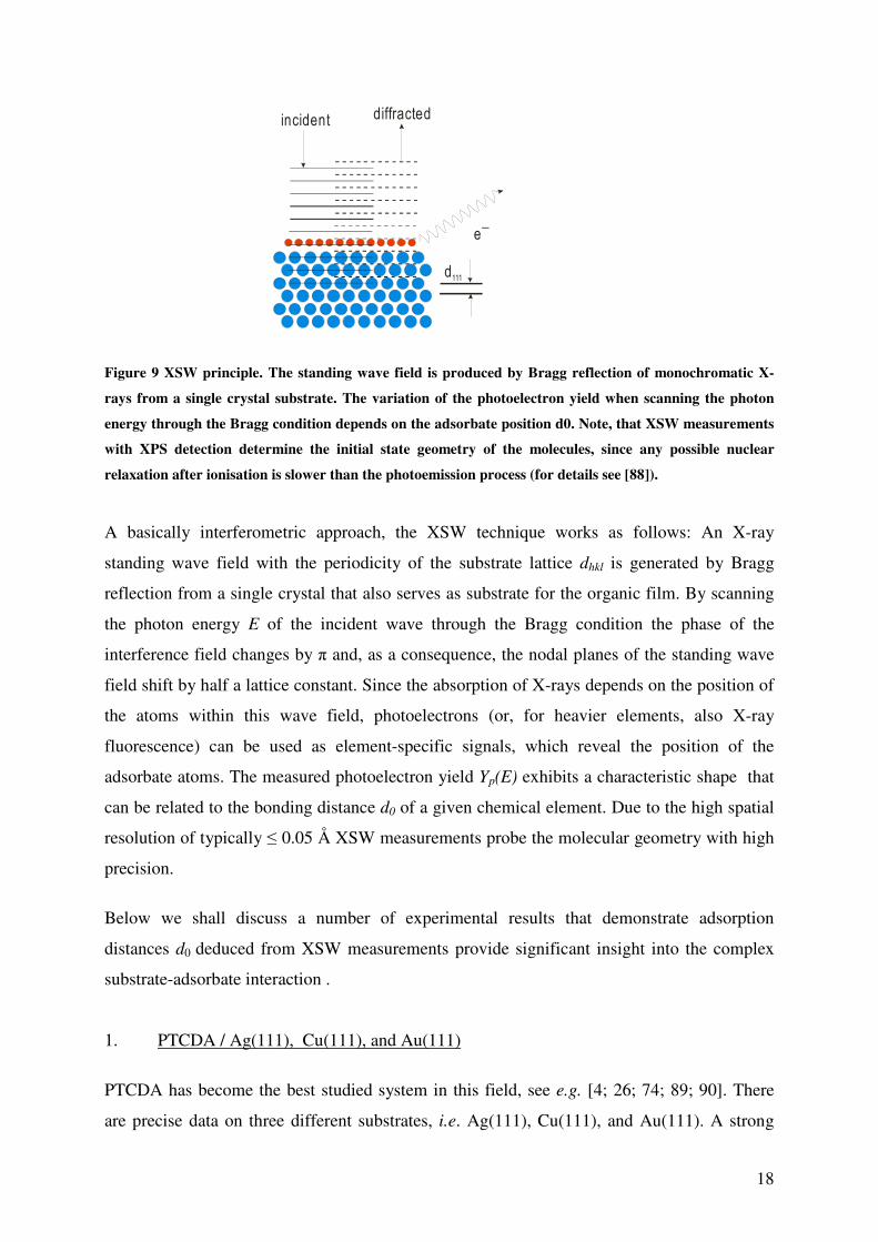
�������� ����� ����
�
��
Figure 9 XSW principle. The standing wave field is produced by Bragg reflection of monochromatic X-
rays from a single crystal substrate. The variation of the photoelectron yield when scanning the photon
energy through the Bragg condition depends on the adsorbate position d0. Note, that XSW measurements
with XPS detection determine the initial state geometry of the molecules, since any possible nuclear
relaxation after ionisation is slower than the photoemission process (for details see [88]).
A basically interferometric approach, the XSW technique works as follows: An X-ray
standing wave field with the periodicity of the substrate lattice dhkl is generated by Bragg
reflection from a single crystal that also serves as substrate for the organic film. By scanning
the photon energy E of the incident wave through the Bragg condition the phase of the
interference field changes by and, as a consequence, the nodal planes of the standing wave
field shift by half a lattice constant. Since the absorption of X-rays depends on the position of
the atoms within this wave field, photoelectrons (or, for heavier elements, also X-ray
fluorescence) can be used as element-specific signals, which reveal the position of the
adsorbate atoms. The measured photoelectron yield Yp(E) exhibits a characteristic shape that
can be related to the bonding distance d0 of a given chemical element. Due to the high spatial
resolution of typically 0.05 Å XSW measurements probe the molecular geometry with high
precision.
Below we shall discuss a number of experimental results that demonstrate adsorption
distances d0 deduced from XSW measurements provide significant insight into the complex
substrate-adsorbate interaction .
1. PTCDA / Ag(111), Cu(111), and Au(111)
PTCDA has become the best studied system in this field, see e.g. [4; 26; 74; 89; 90]. There
are precise data on three different substrates, i.e. Ag(111), Cu(111), and Au(111). A strong
19
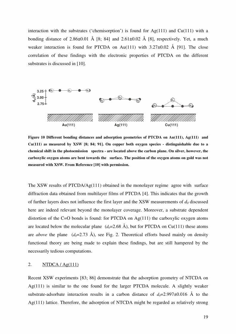
interaction with the substrates (‘chemisorption’) is found for Ag(111) and Cu(111) with a
bonding distance of 2.86±0.01 Å [8; 84] and 2.61±0.02 Å [8], respectively. Yet, a much
weaker interaction is found for PTCDA on Au(111) with 3.27±0.02 Å [91]. The close
correlation of these findings with the electronic properties of PTCDA on the different
substrates is discussed in [10].
OαOβOβ Oα
OβOβ
OαOβ Oβ
Au(111) Ag(111) Cu(111)
3.25
3.00
2.75
d (A
)H
Figure 10 Different bonding distances and adsorption geometries of PTCDA on Au(111), Ag(111) and
Cu(111) as measured by XSW [8; 84; 91]. On copper both oxygen species - distinguishable due to a
chemical shift in the photoemission spectra - are located above the carbon plane. On silver, however, the
carboxylic oxygen atoms are bent towards the surface. The position of the oxygen atoms on gold was not
measured with XSW. From Reference [10] with permission.
The XSW results of PTCDA/Ag(111) obtained in the monolayer regime agree with surface
diffraction data obtained from multilayer films of PTCDA [4]. This indicates that the growth
of further layers does not influence the first layer and the XSW measurements of d0 discussed
here are indeed relevant beyond the monolayer coverage. Moreover, a substrate dependent
distortion of the C=O bonds is found: for PTCDA on Ag(111) the carboxylic oxygen atoms
are located below the molecular plane (d0=2.68 Å), but for PTCDA on Cu(111) these atoms
are above the plane (d0=2.73 Å), see Fig. 2. Theoretical efforts based mainly on density
functional theory are being made to explain these findings, but are still hampered by the
necessarily tedious computations.
2. NTDCA / Ag(111)
Recent XSW experiments [83; 86] demonstrate that the adsorption geometry of NTCDA on
Ag(111) is similar to the one found for the larger PTCDA molecule. A slightly weaker
substrate-adsorbate interaction results in a carbon distance of d0=2.997±0.016 Å to the
Ag(111) lattice. Therefore, the adsorption of NTCDA might be regarded as relatively strong

20
(chemisorption). A non-planar adsorption geometry is also reported for NTCDA [86]. In
essence, the distortion of the C=O bonds in NTCDA is similar to the case of PTCDA on
Ag(111) in which the carboxylic oxygen atoms are located below the molecular plane. Since
no XSW data for Cu(111) or Au(111) are presently available, a substrate dependent distortion
of NTCDA - as found for PTCDA - has not yet been established.
3. F16CuPc / Ag (111) and Cu(111)
The XSW results obtained on F16CuPc show that perfluorinated copper-phthalocyanine
molecules adsorb in a lying down, but significantly distorted configuration on Cu(111) and
Ag(111) surfaces [9]. While on copper (silver) the central carbon rings reside 2.61±0.05 Å
(3.25±0.05 Å) above the substrate, the outer fluorine atoms are located 0.27 Å (0.20 Å)
further away from the surface. These results on F16CuPc are in remarkable contrast to those
on PTCDA on Cu(111) and Ag(111) mentioned above. First, a much larger difference
between the adsorption distances d0 on copper and silver is found. Second, the type of
molecular distortion, i.e. an upward bending of the C-F bonds in F16CuPc, is the same on
copper and silver despite the obviously weaker interaction of F16CuPc with the Ag(111)
surface. As for PTCDA a thorough explanation for the non-planar adsorption structure of the
molecules is still missing. Yet, in [9] it is suggested that the results can be discussed in terms
of the outer carbon atoms in F16CuPc undergoing a partial re-hybridization (sp2 � sp3) with a
concomitant change of the bonding angles.
4. SnPc / Ag(111)
The adsorption geometry and orientation of the non-planar phthalocyanine molecule SnPc has
been measured by XSW [85; 87]. Depending on the preparation conditions SnPc monolayers
exhibit different superstructures and molecular conformations on the Ag(111) surface. For
deposition at 300 °C substrate temperature the carbons atoms are bent away from the surface
[87], whereas for a monolayer of SnPc prepared via desorption of a multilayer film the carbon
atoms are bent towards the surface [85]. This finding is reflected by the different (averaged)
carbon distances found for these conformations of SnPc on Ag(111), i.e., 3.61±0.16 Å [87]
versus 3.17±0.03 Å [85].
To conclude, a rich phenomenology of different adsorption behaviours has been found by
XSW measurements for examples described above: The strength of the substrate-adsorbate
interaction - even for lying-down molecules - varies considerably as is demonstrated by the

21
different bonding distances d0. Adsorption induced distortion of the molecules seems to be the
rule rather than the exception. Therefore, further studies are required to fully understand the
bonding of these systems.
Cu(111) Ag(111) Au(111)
PTCDA 2.66±0.02 Å 2.86±0.01 Å 3.27±0.02 Å
NTCDA 2.997±0.016 Å
F16CuPc 2.61±0.05 Å 3.25±0.05 Å
SnPc (prepared by desorption) 3.17±0.03 Å
SnPc (prepared at 300°C)
3.61±0.16 Å
Table 1 Bonding distances d0 on Cu(111) and Ag(111) measured with the XSW technique. The values
correspond to the (average) carbon distance relative to the Bragg planes of the substrate.
V. Conclusions Organic molecular beam deposition is a complex topic where growth experiments as well as
growth theory are needed for an understanding of the many facets governing the structure
formation of organics. We have not attempted to provide a complete overview of the field or a
comprehensive account of the literature, for which we refer to earlier reviews [12; 13; 15], but
rather we have provided an update on specific issues. In this review we have focused on two
aspects we believe are crucial, namely real-time effects including structure and strain as a
function of time (that is film thickness) and secondly high precision investigations of the first
monolayer (mostly using XSW). Of course many more issues arise in the growth of organic
molecules with their orientational, conformational and vibrational degrees of freedom, and
this is still an open field of research.
Acknowledgements
We wish to thank the many students, collaborators, and colleagues who contributed in various
ways to the work reviewed here. We wish to acknowledge discussions with J. Engstrom and
A. Amassian, valuable comments on the manuscript by E. Oberla, and financial support from
the Deutsche Forschungsgemeinschaft (Focus Programme ‘Organic Field-Effect Transistors’,
Germany) and the EPSRC (UK).

22
References
[1] Koch, N. in this special issue. (2007). [2] Mannsfeld, S. C. B. and Fritz, T. Advanced modelling of epitaxial ordering of organic
layers on crystalline surfaces. Modern Physics Letters B 20, 585-605 (2006). [3] Käfer, D., Ruppel, L., Witte, G. and Wöll, C. Role of Molecular Conformations in
Rubrene Thin Film Growth. Physical Review Letters 95, 166602-4 (2005). [4] Krause, B., Dürr, A. C., Schreiber, F., Dosch, H. and Seeck, O. H. Thermal stability
and partial dewetting of crystalline organic thin films: 3,4,9,10-perylenetetracarboxylic dianhydride on Ag(111). Journal of Chemical Physics 119, 3429-3435 (2003).
[5] Dürr, A. C., Schreiber, F., Ritley, K. A., Kruppa, V., Krug, J., Dosch, H. and Struth, B. Rapid roughening in thin film growth of an organic semiconductor (diindenoperylene). Physical Review Letters 90, 016104 (2003).
[6] Kowarik, S., Gerlach, A., Sellner, S., Schreiber, F., Cavalcanti, L. and Konovalov, O. Real-time observation of structural and orientational transitions during growth of organic thin films. Physical Review Letters 96, 125504 (2006).
[7] Wang, L., Qi, D. C., Liu, L., Chen, S., Gao, X. Y. and Wee, A. T. S. Molecular orientation and ordering during initial growth of copper phthalocyanine on Si(111). Journal of Physical Chemistry C 111, 3454-3458 (2007).
[8] Gerlach, A., Sellner, S., Schreiber, F., Koch, N. and Zegenhagen, J. Substrate dependent bonding distances of PTCDA - A comparative X-ray standing wave study on Cu(111) and Ag(111). Phys. Rev. B 75, 045401 (2007).
[9] Gerlach, A., Schreiber, F., Sellner, S., Dosch, H., Vartanyants, I. A., Cowie, B. C. C., Lee, T.-L. and Zegenhagen, J. Adsorption-Induced Distortion of F16CuPc on Cu(111) and Ag(111): An X-ray Standing Wave Study. Phys. Rev. B 71, 205425 (2005).
[10] Duhm, S. G., A.; Salzmann, I.; Bröcker, B.; Johnson, R. L.; Schreiber, F. & Koch, N. PTCDA on Au(111), Ag(111) and Cu(111): Correlating bonding distance and interfacial charge transfer. Organic Electronics submitted (2007).
[11] Koma, A. Molecular-Beam Epitaxial-Growth of Organic Thin-Films. Progress in Crystal Growth and Characterization of Materials 30, 129-152 (1995).
[12] Forrest, S. R. Ultrathin organic films grown by organic molecular beam deposition and related techniques. Chemical Reviews 97, 1793-1896 (1997).
[13] Schreiber, F. Organic molecular beam deposition: Growth studies beyond the first monolayer. Physica Status Solidi a-Applied Research 201, 1037-1054 (2004).
[14] Fraxedas, J. Perspectives on thin molecular organic films. Advanced Materials 14, 1603-1614 (2002).
[15] Witte, G. and Wöll, C. Growth of aromatic molecules on solid substrates for applications in organic electronics. Journal of Materials Research 19, 1889-1916 (2004).
[16] Dimitrakopoulos, C. D. and Malenfant, P. R. L. (2002). Organic thin film transistors for large area electronics, Advanced Materials, pp. 99-117.
[17] Brütting, W. E. (2005). Physics of Organic Semiconductors. Wiley-VCH. [18] Markov, I. V. (2004). Crystal growth for beginners. 2nd edition. World Scientific
Press. [19] Krug, J. and Michely, T. (2004). Islands, Mounds and Atoms: Patterns and Processes
in Crystal Growth Far From Equilibrium. Springer.
23
[20] Pimpinelli, A. and Villain, J. (1998). Physics of crystal growth. Cambridge University Press.
[21] Barabási, A.-L. and Stanley, H. E. (1995). Fractal Concepts in Surface Growth. Cambridge University Press.
[22] Jackson, K. A. (2004). Kinetic Processes: Crystal Growth, Diffusion, and Phase Transformations in Materials. Wiley.
[23] Jackson, K. A. The interface kinetics of crystal growth processes. Interface Science 10, 159-169 (2002).
[24] Tromp, R. M. and Hannon, J. B. Thermodynamics of nucleation and growth. Surface Review and Letters 9, 1565-93 (2002).
[25] Venables, J. A., Spiller, G. D. T. and Hanbücken, M. Nucleation and growth of thin films. Rep. Prog. Phys. 47, 399-459 (1984).
[26] Krause, B., Durr, A. C., Schreiber, F., Dosch, H. and Seeck, O. H. Late growth stages and post-growth diffusion in organic epitaxy: PTCDA on Ag(1 1 1). Surface Science 572, 385-395 (2004).
[27] Beernink, G., Strunskus, T., Witte, G. and Wöll, C. Importance of dewetting in organic molecular-beam deposition: Pentacene on gold. Applied Physics Letters 85, 398-400 (2004).
[28] Yoshikawa, G., Sadowski, J. T., Al-Mahboob, A., Fujikawa, Y., Sakurai, T., Tsuruma, Y., Ikeda, S. and Saiki, K. Spontaneous aggregation of pentacene molecules and its influence on field effect mobility. Applied Physics Letters 90, 251906-3 (2007).
[29] Hoshino, A., Isoda, S. and Kobayashi, T. Epitaxial growth of organic crystals on organic substrates - polynuclear aromatic hydrocarbons. Journal of Crystal Growth 115, 826-830 (1991).
[30] Hooks, D. E., T. Fritz and M. D. Ward. Epitaxy and Molecular Organization on Solid Substrates. Advanced Materials 13, 227-241 (2001).
[31] Gerstenberg, M. C., Schreiber, F., Leung, T. Y. B., Bracco, G., Forrest, S. R. and Scoles, G. Organic semiconducting thin film growth on an organic substrate: 3,4,9,10-perylenetetracarboxylic dianhydride on a monolayer of decanethiol self-assembled on Au(111). Physical Review B 61, 7678-7685 (2000).
[32] Schreiber, F., Gerstenberg, M. C., Dosch, H. and Scoles, G. Melting point enhancement of a self-assembled monolayer induced by a van der Waals bound capping layer. Langmuir 19, 10004-10006 (2003).
[33] Schreiber, F., Gerstenberg, M. C., Edinger, B., Toperverg, B., Forrest, S. R., Scoles, G. and Dosch, H. Phase-sensitive surface X-ray scattering study of a crystalline organic-organic heterostructure. Physica B-Condensed Matter 283, 75-78 (2000).
[34] Killampalli, A. S. and Engstrom, J. R. Nucleation of pentacene thin films on silicon dioxide modified with hexamethyldisilazane. Applied Physics Letters 88 (2006).
[35] Käfer, D., Ruppel, L. and Witte, G. Growth of pentacene on clean and modified gold surfaces. Physical Review B (Condensed Matter and Materials Physics) 75, 085309-14 (2007).
[36] Ruiz, R., Nickel, B., Koch, N., Feldman, L. C., Haglund, R. F., Kahn, A. and Scoles, G. Pentacene ultrathin film formation on reduced and oxidized Si surfaces. Physical Review B 67, art. no.-125406 (2003).
[37] Klauk, H., Zschieschang, U., Pflaum, J. and Halik, M. Ultralow-power organic complementary circuits. 445, 745-748 (2007).
[38] Aumann, C. E., Kariotis, R. and Lagally, M. G. Rate equation modeling of interface width. Journal of Vacuum Science & Technology A: Vacuum, Surfaces, and Films 7, 2180-2185 (1989).
[39] Krug, J. Origins of scale invariance in growth processes. Advances in Physics 46, 139-282 (1997).

24
[40] Krug, J. Power laws in surface physics: The deep, the shallow and the useful. arXiv:cond-mat/0403267 v1 10 Mar 2004 (2004).
[41] Ruiz, R., Nickel, B., Koch, N., Feldman, L. C., Haglund, R. F., Jr., Kahn, A., Family, F. and Scoles, G. Dynamic scaling, island size distribution, and morphology in the aggregation regime of submonolayer pentacene films. Physical Review Letters 91, 136102/1-4 (2003).
[42] Yim, S. and Jones, T. S. Anomalous scaling behavior and surface roughening in molecular thin-film deposition. Physical Review B 73, 161305(R) (2006).
[43] Lafouresse, M. C., Heard, P. J. and Schwarzacher, W. Anomalous Scaling for Thick Electrodeposited Films. Physical Review Letters 98, 236101-4 (2007).
[44] Kowarik, S., Gerlach, A., Sellner, S., Schreiber, F., Pflaum, J., Cavalcanti, L. and Konovalov, O. Anomalous roughness evolution of rubrene thin films observed in real time during growth. Physical Chemistry Chemical Physics 8, 1834 - 1836 (2006).
[45] Meyer zu Heringdorf, F. J., Reuter, M. C. and Tromp, R. M. Growth dynamics of pentacene thin films. Nature 412, 517-20. (2001).
[46] Braun, W., Däweritz, L. and Ploog, K. H. Origin of electron diffraction oscillations during crystal growth. Physical Review Letters 80, 4935-4938 (1998).
[47] Casalis, L., Danisman, M. F., Nickel, B., Bracco, G., Toccoli, T., Iannotta, S. and Scoles, G. Hyperthermal Molecular Beam Deposition of Highly Ordered Organic Thin Films. Physical Review Letters 90, 206101 (2003).
[48] Söhnchen, S., Lukas, S. and Witte, G. Epitaxial growth of pentacene films on Cu(110). Journal of Chemical Physics 121, 525-534 (2004).
[49] Karl, N. (2001). Organic Electronic Materials in Farchioni, R. and Grosso, G. (Eds), Organic Electronic Materials, Springer.
[50] Ruiz, R., Mayer, A. C., Malliaras, G. G., Nickel, B., Scoles, G., Kazimirov, A., Kim, H., Headrick, R. L. and Islam, Z. Structure of pentacene thin films. Applied Physics Letters 85, 4926-4928 (2004).
[51] Ruiz, R., Choudhary, D., Nickel, B., Toccoli, T., Chang, K.-C., Mayer, A. C., Clancy, P., Blakely, J. M., Headrick, R. L., Iannotta, S. and Malliaras, G. G. Pentacene Thin Film Growth. Chem. Mater. 16, 4497-4508 (2004).
[52] Yoshida, H., Inaba, K. and Sato, N. X-ray diffraction reciprocal space mapping study of the thin film phase of pentacene. Applied Physics Letters 90, 181930-3 (2007).
[53] Schiefer, S., Huth, M., Dobrinevski, A. and Nickel, B. Determination of the Crystal Structure of Substrate-Induced Pentacene Polymorphs in Fiber Structured Thin Films. J. Am. Chem. Soc. (2007).
[54] Pratontep, S., Brinkmann, M., Nuesch, F. and Zuppiroli, L. Correlated growth in ultrathin pentacene films on silicon oxide: Effect of deposition rate. Physical Review B 69, 165201-7 (2004).
[55] Killampalli, A. S., Schroeder, T. W. and Engstrom, J. R. Nucleation of pentacene on silicon dioxide at hyperthermal energies. Applied Physics Letters 87, 033110 (2005).
[56] Mayer, A. C., Kazimirov, A. and Malliaras, G. G. Dynamics of Bimodal Growth in Pentacene Thin Films. Physical Review Letters 97, 105503-4 (2006).
[57] Mayer, A. C., Ruiz, R., Headrick, R. L., Kazimirov, A. and Malliaras, G. G. Early stages of pentacene film growth on silicon oxide. Organic Electronics 5, 257-263 (2004).
[58] Mayer, A. C., Ruiz, R., Zhou, H., Headrick, R. L., Kazimirov, A. and Malliaras, G. G. Growth dynamics of pentacene thin films: Real-time synchrotron x-ray scattering study. Physical Review B 73, 205307 (2006).
[59] Kowarik, S., Gerlach, A., Leitenberger, W., Hu, J., Witte, G., Wöll, C., Pietsch, U. and Schreiber, F. Energy-dispersive X-ray reflectivity and GID for real-time growth studies of pentacene thin films. Thin Solid Films 515, 5606-5610 (2007).

25
[60] Bouchoms, I. P. M., Schoonveld, W. A., Vrijmoeth, J. and Klapwijk, T. M. Morphology identification of the thin film phases of vacuum evaporated pentacene on SiO2 substrates. Synthetic Metals 104, 175-178 (1999).
[61] Kowarik et al., S. Real-time studies of thin film growth: Measurement and analysis of X-ray growth oscillations beyond the anti-Bragg point. submitted
[62] Cohen, P. I., Petrich, G. S., Pukite, P. R., Whaley, G. J. and Arrott, A. S. Birth-death models of epitaxy : I. Diffraction oscillations from low index surfaces. Surface Science 216, 222-248 (1989).
[63] Markov, I. V. (1994). Crystal growth for beginners : fundamentals of nucleation, crystal growth and epitaxy. World Scientific.
[64] Dürr, A. C., Schreiber, F., Kelsch, M. and Dosch, H. Optimized preparation of cross-sectional TEM specimens of organic thin films. Ultramicroscopy 98, 51-55 (2003).
[65] Dürr, A. C., Schreiber, F., Munch, M., Karl, N., Krause, B., Kruppa, V. and Dosch, H. High structural order in thin films of the organic semiconductor diindenoperylene. Applied Physics Letters 81, 2276-2278 (2002).
[66] Münch, M. PhD-thesis (2001). Strukturelle Beeinflussung der elektrischen Transporteigenschaften dünner organischer Schichten. Universität Stuttgart.
[67] Drummy, L. F. and Martin, D. C. Thickness-Driven Orthorhombic to Triclinic Phase
Transformation in Pentacene Thin Films. Advanced Materials 17 (2005). [68] Dürr, A. C., Nickel, B., Sharma, V., Taffner, U. and Dosch, H. Observation of
competing modes in the growth of diindenoperylene on SiO2. Thin Solid Films 503, 127-132 (2006).
[69] Umbach, E. Characterization of organic overlayers on welldefined substrates. Prog. Surf. Sci. 35, 113-127 (1991).
[70] Krause, B., Schreiber, F., Dosch, H., Pimpinelli, A. and Seeck, O. H. Temperature dependence of the 2D-3D transition in the growth of PTCDA on Ag(111): A real-time X-ray and kinetic Monte Carlo study. Europhysics Letters 65, 372-378 (2004).
[71] D. Schlettwein, A. Back, B. Schilling, T. Friz and Armstrong, N. R. Ultrathin films of perylenedianhydride and perylenebis(dicarboximide) dyes on (001) alkali halide surfaces. Chem. Mater. 10, 601-612 (1998).
[72] Kilian, L., Umbach, E. and Sokolowski, M. A refined structural analysis of the PTCDA monolayer on the reconstructed Au(111) surface - "Rigid or distorted carpet?" Surface Science 600, 2633-2643 (2006).
[73] Fenter, P., Schreiber, F., Zhou, L., Eisenberger, P. and Forrest, S. R. In situ studies of morphology, strain, and growth modes of a molecular organic thin film. Physical Review B 56, 3046-3053 (1997).
[74] Krause, B., Durr, A. C., Ritley, K., Schreiber, F., Dosch, H. and Smilgies, D. Structure and growth morphology of an archetypal system for organic epitaxy: PTCDA on Ag(111). Physical Review B 66, art. no.-235404 (2002).
[75] Krause, B., Durr, A. C., Ritley, K. A., Schreiber, F., Dosch, H. and Smilgies, D. On the coexistence of different polymorphs in organic epitaxy: alpha and beta phase of PTCDA on Ag(111). Applied Surface Science 175, 332-336 (2001).
[76] Krause, B. PhD-thesis (2002). Growth and Structure of the Organic Molecule PTCDA on Ag(111). Universität Stuttgart.
[77] Kilian, L., Umbach, E. and Sokolowski, M. Molecular beam epitaxy of organic films
investigated by high resolution low energy electron diffraction (SPA-LEED): 3,4,9,10-perylenetetracarboxylicacid-dianhydride (PTCDA) on Ag(111). Surface Science 573, 359-378 (2004).

26
[78] Eremtchenko, M., Schaefer, J. A. and Tautz, F. S. Understanding and tuning the epitaxy of large aromatic adsorbates by molecular design. Nature (London, United Kingdom) 425, 602-605 (2003).
[79] Tan, S. and Lam, P. M. Monte Carlo simulation of three-dimensional islands. Physical Review B 60 (1999).
[80] Zegenhagen, J. Surface structure determination with X-ray standing waves. Surf. Sci. Rep. 18, 199 (1993).
[81] Bedzyk, M. J. C., L. (2002). X-ray standing wave studies of minerals and mineral surfaces; principles and applications, Rev. Mineral. Geochem., pp. 221.
[82] Woodruff, D. P. Surface structure determination using x-ray standing waves. Rep. Prog. Phys. 68, 743 (2005).
[83] Stanzel, J. W., W.; Kilian, L.; Meyerheim, H. L.; Kumpf, C. & Umbach, E. Chemisorption of NTCDA on Ag(111): a NIXSW study including non-dipolar and electron-stimulated effects. Surf. Sci. Lett. 571, 311 (2004).
[84] Hauschild, A. K., K.; Cowie, B. C. C.; Rohlfing, M.; Tautz, F. S. & Sokolowski, M. Molecular Distortions and Chemical Bonding of a Large $$-Conjugated Molecule on a Metal Surface. Phys. Rev. Lett. 94, 36106 (2005).
[85] Stadler, C., Hansen, S., Pollinger, F., Kumpf, C., Umbach, E., Lee, T.-L. and Zegenhagen, J. Structural investigation of the adsorption of SnPc on Ag(111) using normal-incidence x-ray standing waves. Phys. Rev. B 74, 035404 (2006).
[86] Stadler, C., Hansen, S., Schöll, A., Lee, T.-L., Zegenhagen, J., Kumpf, C. and Umbach, E. Molecular distortion of NTCDA upon adsorption on Ag(111): a normal incidence x-ray standing wave study. New J. Phys. 9, 50 (2007).
[87] Woolley, R. A. J., Martin, C. P., Miller, G., Dhanak, V. R. and Moriarty, P. J. Adsorbed molecular shuttlecocks: An NIXSW study of Sn phthalocyanine on Ag(111) using Auger electron detection. Surf. Sci. 601, 1231 (2007).
[88] Schreiber, F., Gerlach, A., Koch, N., Zojer, E., Sokolowski, M., Tautz, F. S., Rohlfing, M. and Umbach, E. Comment on "Electron Core-Hole Interaction and Its Induced Ionic Structural Relaxation in Molecular Systems under X-Ray Irradiation". Phys. Rev. Lett. 99, 059601 (2007).
[89] Kilian, L. U., E. & Sokolowski, M. Molecular beam epitaxy of organic films investigated by high resolution low energy electron diffraction (SPA-LEED): 3,4,9,10-perylenetetracarboxylicacid-dianhydride (PTCDA) on Ag(111). Surf. Sci. 573, 359 (2004).
[90] Zou, Y. K., L.; Schöll, A.; Schmidt, Th.; Fink, R. & Umbach, E. Chemical bonding of PTCDA on Ag surfaces and the formation of interface states. Surf. Sci. 600, 1240 (2006).
[91] Henze, S. K. M., Bauer, O., Lee, T. L., Sokolowski, M. and Tautz, F. S. Vertical bonding distances of PTCDA on Au(111) and Ag(111): Relation to the bonding type. Surface Science 601, 1566-1573 (2007).