oskar dahlin848291/fulltext01.pdf · 2015-08-24 · analyzed by xrd on thin film and mesoporous...
TRANSCRIPT

Master thesis
Synthesis and characterization of non-toxic organic
metal halide semiconductors for solar cell applications
Oskar Dahlin
KTH
Stockholm
2015
Master thesis
Title: Synthesis and characterization of non-toxic organic
metal halide semiconductors for solar cell applications
Supervisor: James Gardner and Majid Safdari
Student: Oskar Dahlin
Date: 2015-07-30
Examiner: James Gardner

Abstract
The endeavor to have more efficient solar cells and as environmentally beneficial as
possible are the driving forces for this work. The way to reach this is by research to better
the understanding of the mechanisms and parameters that govern the performance of solar
cells. New materials are essential to develop because the current ones lack stability and are
water, temperature and UV-radiation sensitive. In this work the lead (Pb2+), which is
poisonous and hazardous is intended to be replaced in the organic metal halide (OMH)
perovskite structure. This is tested with gold or silver combined with bismuth and silver
by itself. Also trimethylsulfonium gold or silver iodides are investigated. The
methylammonium cation is also substituted to cesium. The perovskite material both
absorbs light and transports charges in the solar cells. Materials based on AuI/AgI, BiI3
and CH3NH3I and AuI/AgI and [Me3S]I and AgI, BiI3 and CsI were synthesized and
analyzed by XRD on thin film and mesoporous substrate and Raman spectroscopy to
determine material structure and bonding. J-V measurements were performed to see the
function in solar cells. After this conductivity and absorption parameters were determined
by an electrical conductivity test and UV-vis absorption spectroscopy.
XRD measurements indicate that the perovskite structure could have been obtained
because the materials match with the XRD spectra of [20] foremost T3, T5 and T6, Cs1
and Cs2. In T7 some new structure is formed. The bismuth could be partially substituted
by silver as the metal cation. The samples are quite amorphous, but still containing
crystalline peaks, the product material could be a mixture of a crystalline and an amorphous
phase. The crystalline phase could have the desired perovskite structure. To have
mesoporous TiO2 as substrate seem to enhance a more crystalline structured material. All
the materials seem to have formed some new structures because the pure reactants does
not seem to be present, exceptions could be P1 and T1 that contained AuI. The change of
cation from methylamine to cesium though results in a shift of the peak positions because
of the change of cation size as in [20], but the structure is most likely the same.
Raman spectroscopy indicate that there is a change in structure, some new bond being
present, when increasing the methylamine ratio for the presumed methylammonium silver
bismuth iodide perovskites. This concerns materials T5, T6, T7 with increasing ratio of
methylamine. This new bond is most pronounced in T7 where the methylamine content is
the highest. Both Silver and bismuth iodide bonds seem to be present and cannot be
coupled to be the pure reactants recrystallizing and some new bonds of these are present
in all materials to some extent. The organic bond vibration has low intensity and might
indicate that there is not so much organic cation present in the product and thus the
probability of having the desired product anion decreases.
The solar cells made with Spiro-OMeTAD were 700-4000 times more efficient than those
made with Sulphur polymer HTM.
Solar cells made with Spiro-OMeTAD as HTM gives slightly higher efficiency when
increasing the methylammonium cation ratio. For cesium as cation the combined metal
cation constellation with bismuth and silver gives a little higher efficiency than bismuth
alone. Methylammonium as cation gives a higher efficiency than cesium.
Solar cells made with Sulphur polymer HTM show approximately 3-30 times higher
efficiency with methylammonium as cation compared to cesium as cation. HTM material
seem to affect the perovskite material making some of the cells completely transparent and
some of them paler, water in the solvent chlorobenzene can be a possible explanation. The
transparency can be the reason for the low efficiency obtained for the solar cells. Also the
measurement methodology of these solar cells can also have been false, measuring the
contacts, and the etching procedure could be another source of this.
The solar cells had quite low efficiencies compared to [20], although same presumed
material and procedure has been used and thus there might be something wrong in the
accuracy of the manufacturing. The cells should probably been made several times and
possible sources of error should be analyzed and corrected for.
The materials were all relatively conductive. P1 gave the highest conductivity, almost three
times higher than for methylammonium lead iodide that has a conductivity of 1,1x10⁻⁴
s/cm [3]. Increasing the methylammonium ratio gave an increase of the conductivity both
with bismuth and silver as metal cations and silver alone. The increase of the
methylammonium ratio might result in a new structure formed which has lattice planes that
are more conductive. A change of gold to silver for the trimethylsulfonium iodide materials
gave a large decrease in conductivity.
The materials have different absorption curves meaning that they have different bandgaps
and this indicates differences in structure. The bandgaps of all materials are indirect
contrary to what is proven to be the case for perovskites that are believed to have direct
bandgaps in general. To have indirect bandgaps requires a shift in momentum in the
electronic transitions and is not as beneficial as having direct bandgaps. Compared to
methylammonium lead iodide that has a direct bandgap of 1,6 eV, the bandgaps are at least
0,5 eV higher and range between 2,2-2,36 eV. P1 had a low bandgap of 1,6 eV meaning it
absorbs a wide range of wavelengths.
The conductivity does not seem to be the obstacle and the cells that are not transparent
absorb light. It is highly possible that the low solar cell performance, at least to a certain
extent, has to do with the production process. The low scan rate could also affect the low
efficiencies and HTM Spiro-OMeTAD should be used.
Currently the efficiency of the perovskite materials with silver/bismuth, gold/bismuth and
silver are too low, and not able to substitute lead in the perovskite structure solar cells.
Neither trimethylsulfonium gold or silver iodide cells nor cesium perovskites have enough
efficiency at present. The conductivities for the materials are promising and the materials
that are not completely transparent absorb light.

Sammanfattning
Strävan att utveckla effektivare solceller och så miljövänliga som möjligt är drivkrafterna
för det här arbetet. För att uppnå detta krävs forskning för att förbättra förståelsen för vilka
mekanismer och parametrar som styr hur väl solcellerna fungerar. Det är nödvändigt att ta
fram nya material, då de nuvarande brister i stabilitet, de är framförallt känsliga för vatten,
temperatur och UV-strålning. I det här arbetet är syftet att byta ut bly (Pb2+), som är giftig
och kopplad till hälsorisker, i den organiska metall halid (OMH) perovskit strukturen.
Detta görs med guld eller silver i kombination med vismut och silver självt. Även
trimetylsulfonium- guld eller silver undersöks. Metylammonium katjonen substitueras
också mot cesium. Perovskit material absorberar både ljus och transporterar laddningar i
solceller. Material baserade på AuI/AgI, BiI3 och CH3NH3I and AuI/AgI och [Me3S]I and
AgI, BiI3 and CsI syntetiserades. Dessa analyserades, med XRD på dels ett substrat av tunn
film och dels ett mesoporöst och Raman spektroskopi, för att bestämma strukturen på
materialet och bindningar. J-V mätningar utfördes för att se hur materialen fungerade som
solceller. Efter detta utfördes mätningar av konduktiviteten och absorptions parametrar
bestämdes genom ett elektriskt konduktivitetstest respektive UV-vis absorptions
spektroskopi.
XRD mätningarna indikerar att perovskit strukturen kan ha erhållits eftersom spektrumen
överensstämmer med de i [20], framförallt för T3, T5 och T6, Cs1 och Cs2.
I T7 bildas någon ny struktur. Vismut skulle kunna vara delvis utbytt mot silver som
metalkatjon. Proven är relativt amorfa, men uppvisar kristallina toppar och produkten
skulle kunna vara en blandning av en kristallin och amorf fas, där den kristallina fasen
skulle kunna ha den eftersträvade perovskit strukturen. Mesoprös TiO2 som substrat verkar
öka graden av kristallinitet hos materialen. Samtliga material verkar ha bildat någon ny
struktur eftersom reaktanterna i sin rena form inte verkar finnas. Undantag skulle kunna
vara P1 och T1, vilka innehåller AuI. Bytet av katjon från metylammonium mot cesium
resulterar i ett skifte av topparna troligen beroende av skillnaden i storlek mellan
katjonerna, liksom påvisas i [20], men strukturen är förmodligen densamma.
Raman spektroskopin indikerar en förändring i strukturen, någon ny bindning finns, hos
materialen när metylammonium andelen ökas för de förmodade metylammonium silver
vismut jodid perovskiterna. Detta gäller materialen T5, T6, T7, där andelen
metylammonium ökar. Den nya bindningen är mest uttalade i T7, där metylammonium
andelen är den högsta. Både silver och vismut jodid bindningar verkar finnas och kan inte
kopplas till att de rena reaktanterna har rekristalliserats och nya bindningar av dessa finns
i alla material till en viss grad. Den organiska bindningens vibration har låg intensitet och
kan tyda på att det inte finns så mycket organisk katjon i produkten och således minskar
sannolikheten att ha den eftersträvade anjon produkten.
Solcellerna gjorda med Spiro-OMeTAD var 700-4000 gånger mer effektiva än dom gjorda
med Svavel polymer HTM.
För solcellerna gjorda med Spiro-OMeTAD som HTM ger en ökning av metylammonium
katjon andelen en ökad effektivitet. För cesium som katjon med den kombinerade
metalkatjon konstellationen med vismut och silver, blir effektiviteten högre än om vismut
är metalkatjon självt. Metylammonium som katjon ger en högre effektivitet än cesium.
Solceller gjorda med Svavel polymer HTM visar ungefär 3-30 gånger högre effektivitet
med metylammonium som katjon jämfört med cesium som katjon. HTM materialet verkar
påverka perovskit materialet och göra några av cellerna helt transparenta och de andra
blekare. Klor benzen användes som lösningsmedel och denna kan ha innehållit vatten och
kan vara orsaken till färgskiftningen. Detta kan vara orsaken till den låga verkningsgraden
som erhölls för solcellerna. En annan möjlig förklaring skulle kunna vara metoden för

mätningarna. Denna kan ha varit felaktig, då kontakten troligen har varit det som har mätts
och etsningsprocessen skulle kunna vara en orsak till detta.
Solcellerna uppvisar ganska låg effektivitet i jämförelse med [20], trots att samma material
och procedur har använts och således kan det vara något fel i precisionen av
framställningen. Cellerna skulle förmodligen gjorts om ett antal gånger och möjliga
felkällor borde utretts och åtgärdats.
Materialen var överlag relativt konduktiva. P1 gav den högsta konduktiviteten, nära tre
gånger högre än metylammonium bly jodid, som har en konduktivitet på 1,1x10⁻⁴ s/cm [3].
En ökning av andelen metylammonium gav en ökning av konduktiviteten både med vismut
och silver som metalkatjon och silver självt. Ökningen av andelen metylammonium skulle
kunna resultera i ett en ny struktur uppkommer som har plan som är mer konduktiva.
Utbytet av guld mot silver för trimetylsulfonium jodid materialen gav en markant sänkning
av konduktiviteten.
Materialen har olika absorptionskurvor vilket innebär att de har olika bandgap och detta
indikerar olikheter i strukturen. Bandgapen för alla material är indirekta, trots att
bandgapen för perovskiter i regel är direkta. Att ha indirekta bandgap kräver ett skifte i
momentum i de elektroniska energiöverföringarna och är inte så fördelaktigt som att ha
direkta bandgap. I jämförelse med metylammonium bly jodid, som har ett direkt bandgap
på 1,6eV, är bandgapen minst 0,5 eV högre och varierar mellan 2,2-2,36 eV. P1 hade ett
lågt värde på bandgapet, 1,6 eV, vilket innebär absorption av ett brett spektrum av
våglängder.
Konduktiviteten verkar inte vara den faktor som är orsaken till den låga effektiviteten hos
solcellerna och de celler som inte är transparenta absorberar ljus. Det är högst troligt att
den låga effektiviteten har sin förklaring, åtminstone delvis, i produktionsprocessen för
solcellerna. Den relativt låga skanningshastigheten kan också vara en orsak för den låga
effektiviteten och HTM Spiro-OMeTAD bör användas.
I dagsläget är effektiviteten för perovskitmaterialen med silver/vismut, guld/vismut och
silver för låg och har inte möjlighet substituera bly i perovskit solceller. Inte heller
trimetylsulfonium guld eller silver jodid cellerna och inte heller cesium perovskiternas
effektivitet räcker till i dagsläget. Konduktiviteten för materialen är lovande och materialen
som inte är transparenta absorberar ljus.

Acknowledgements
Throughout the project I have had very much assistance from my both supervisors James
Gardner and Majid Safdari. They have always been helpful and supporting and have
provided me with constructive feedback and good ideas. I have worked together with Majid
Safdari to a large extent especially in the experiments and by that I have learned much and
had a very good time. The spirit and working climate at the department at KTH have also
been good. I have participated in a solar cell congress at Uppsala University between
Sweden and Belgium that gave me much insight and inspiration into solar cells. I have also
got the change to take part in the solar cell group at KTH lead by Lars Kloo with weekly
meetings and interesting and actual discussions of the ongoing science in the field of solar
cells.
Table of contents 1 Introduction ..................................................................................................................................1
1.1 Aim of project ........................................................................................................................1
1.2 Background on perovskites ....................................................................................................1
1.3 Previous work done on materials for solar cell applications .................................................3
1.4 Function mechanism of perovskite solar cells .......................................................................4
1.5 Structure of perovskite solar cells .........................................................................................6
1.6 Efficiency determination of solar cells ...................................................................................7
1.7 X-ray diffraction .....................................................................................................................7
1.8 Raman Spectroscopy .............................................................................................................8
1.9 UV-vis spectroscopy ...............................................................................................................8
2 Experiment ................................................................................................................................. 10
2.1 Synthesis ....................................................................................................................... 10
2.1.1 CH3NH3(Ag0.5Bi0.5)I3, CH3NH3Ag2I3, Cs3Bi2I9 and CsAgBiI5 .............................................. 10
2.1.2 P1 [Me3S]2[AuI4][I3] ................................................................................................ 11
2.1.3 P2 [Me3S]3[AgI4][I3] ................................................................................................ 11
2.2 Preparation of solar cells .................................................................................................... 12
2.2.1 Preparation of substrate ............................................................................................. 12
2.2.2 Blocking layer of TiO2 ................................................................................................... 12
2.2.3 Mesoporous layer of TiO2 and inserted perovskite ..................................................... 12
2.2.4 Hole transporting material Spiro-OMeTAD ................................................................. 13
2.2.5 Hole transporting material Sulphur polymer .............................................................. 13
2.2.6 Ag counter electrode ................................................................................................... 14
2.3 Characterization .................................................................................................................. 14
2.3.1 X-Ray diffraction .......................................................................................................... 14
2.3.2 Raman Scattering ........................................................................................................ 15
2.3.3 Solar cell performance ................................................................................................ 15
2.3.4 Electrical conductivity test .......................................................................................... 15
2.3.5 UV- vis Absorption measurement ............................................................................... 17
3 Result and discussion ................................................................................................................. 17
3.1 Results of XRD ..................................................................................................................... 17
3.1.1 Discussion of XRD ........................................................................................................ 22
3.2 Results of Raman spectroscopy .......................................................................................... 24
3.2.1 Discussion of Raman spectroscopy ............................................................................. 25
3.3 Results of solar cell performance .................................................................................. 27
3.3.1 Results of solar cells with Spiro-OMeTAD as HTM ................................................ 27
3.3.2 Discussion of solar cell performance with Spiro-OMeTAD HTM ................................. 28
3.3.3 Results of solar cells with Sulphur polymer as HTM ................................................... 29
3.3.4 Pictures of solar cells with Sulphur polymer HTM ................................................ 31
3.3.5 Discussion of solar cell performance with Sulphur polymer HTM ........................ 31
3.3.6 Overall discussion of solar cell performance ........................................................ 32
3.4 Result of conductivity measurements and calculation ....................................................... 33
3.4.1 Discussion of conductivity measurement and calculation .......................................... 34
3.5 Result of UV-vis absorption measurements and calculation .............................................. 35
3.5.1 Pictures of cells for UV-vis absorption measurement ................................................. 36
3.5.2 Discussion of UV-vis absorption measurement and calculation ................................. 36
4 Conclusions ................................................................................................................................ 39
5 Future research .......................................................................................................................... 40
6 References .................................................................................................................................. 41
Appendix 1. ................................................................................................................................... 43
Appendix 2. ................................................................................................................................... 43
Appendix 3. ................................................................................................................................... 43
Appendix 4. ................................................................................................................................... 43
Appendix 5. ................................................................................................................................... 43
Appendix 6. ................................................................................................................................... 43
Appendix 7. ................................................................................................................................... 43
Appendix 8. ................................................................................................................................... 43
Appendix 9. ................................................................................................................................... 43
Abbreviations
AM Air Mass
AgI Silver iodide
AuI Gold iodide
BiI3 Bismuth iodide
CH3NH3AgBiI3 Methylammonium silver bismuth iodide
CH3NH3AuBiI3 Methylammonium gold bismuth iodide
CH3NH3I Methylammonium iodide
DMF Dimethylformamide
DMSO Dimethyl sulfoxide
FF Fill factor
FTO Fluorine doped Tin dioxide
GBL Gamma-butyrolactone
HCl Hydrochloric acid
HI Hydrogen iodide
HTM Hole Transport Material
I2 Molecular iodine
J-V Current density-voltage
LiN (CF3SO2)2 (Lithium bis (trifluoromethanesulfonyl) imide)
LUMO Lowest Unoccupied Molecular Orbital
[Me3S]2[AuI4][I3] Trimethylsulfonium gold (III) iodide
N2 Nitrogen gas
OMH Organic metal halide
SEM Scanning Electron Microscopy
T1 T1”(CH3NH3+: Au+:Bi3+:I-:1:1:1:156,6)”
T3 T3”(CH3NH3+:Ag+:Bi3+:I-:1:1:1:80.8)”
T4 T4”(CH3NH3+:Ag+:Bi3+:I-:1:1:0,2:80.8)”
T5 T5”(CH3NH3+:Ag+:Bi3+:I-:5:1:1:79,8)”
T6 T6”(CH3NH3+:Ag+:Bi3+:I-:10:1:1:79,8)”
T7 T7”(CH3NH3+:Ag+:Bi3+:I-:15:1:1:79,8)”
T8 T8”(CH3NH3+:Ag+:Bi3+:I-:1:1:5:79,8)”
T9 T9”(CH3NH3+:Ag+:Bi3+:I-:15:1:10:79,8)”
T11 T11”(CH3NH3+:Ag+:I-:1:1:76,8)”
T12 T12”(CH3NH3+:Ag+:I-:5:1:76,8)”
P1 P1”( [Me3S]I:AuI:I2:1:1:3)”
P2 P2”( [Me3S]I:AgI:I2:1:1:1,5)”
Cs1 Cs1”(Cs+:Bi3+:I-:1:1:383)”
Cs2 Cs2”(Cs+:Bi3+:I-:1:0,2:0,8:382,6)”
t-BP 4-tert-butylpyridine
TiO2 Titanium dioxide
UV-vis Ultraviolet visible
XRD X-ray diffraction

1
1 Introduction
The endeavor to have more efficient and stable solar cells and as environmentally beneficial as
possible are the driving forces for this master thesis. The way to reach this is by research to
better the understanding of the photosensitizing and charge transporting materials mechanisms
and parameters that govern the performance of solar cells.
1.1 Aim of project
The aim of this project is to synthesize Pb2+-free materials for use in solar cells as
semiconductors. The materials should both absorb light and transport charges. Currently the
materials lacks stability and are water, temperature and UV-radiation sensitive. Materials
having the perovskite structure have been proven to function in solar cells. The synthesized
materials are going to be analyzed by X-ray diffraction on thin films of TiO2 and incorporated
into mesoporous TiO2, Raman spectroscopy and tested in solar cells. The conductivity and UV-
vis absorption are also going to be investigated.
1.2 Background on perovskites
Perovskite is CaTiO3 and the crystal structure for organic metal halide perovskites is shown in
Figure 1. The structure is a metal cation surrounded by six iodide ions in an octahedron and the
octahedron is inside a cube, which corners are organic. The metal cation and the iodide ions are
chemically bound to each other while the organic cation is electrostatically attracted to this
complex. The 3 dimensional structure is desired and is shown in the lattice structure to the right
in Figure 1. The 3 dimensional structure possess better charge transport properties, minimizing
the excitonic traps compared to 2 dimensional structures. [2] Also one dimensional structures
could be obtained.
The generic formula for perovskites is AMX3; A is a large monovalent cation, M is a metal(II),
and X is a halide. The formula is flexible such that materials of the form AMA(y)MB(1-y)X3 should
be synthetically accessible; MA = Au(I) or Ag(I); MB = Bi(III) and A = CH3NH3+ or alkaline
metal and X = halide. Lead(II) has previously been used as the metal cation but is intended to
be replaced by non-toxic elements. Sn has also been tried but its stability is the major drawback.
Au(I) or Ag(I) together with Bi(III) will be tested which are less hazardous than lead. Due to
their similar sizes and their average charge, AuI(I) or AgI(I) with Bi(III) may be substituted for
Pb(II) in the perovskite structure. The ratios of the different reactants are varied and this is
expected to give rise to different structures and properties of the material. Energy levels,
absorption and bandgaps tend to change and can thus be researched and modified. The size of
elements tend to affect the material properties. The atomic radius of the elements are: lead 1.54
Å, silver 1.65 Å, bismuth 1.43 Å and gold 1.74 Å and thus they are relatively equally sized.
[15]
The most common halides are I, Br and Cl and they can also be combined which has proven to
promote stability and transport of charge. The halides give rise to different bandgaps and
different materials within the perovskite assembly. [3, 9, 11, 14, 16]

2
Figure 1. The ideal organic metal halide perovskite structure. [5]
The major appeal of perovskite solar cells is the relatively simple, inexpensive synthesis to
prepare the materials and manufacture solar cells compared to the most common crystalline
silicon solar cells whose production is comparably expensive. The temperatures required for
the syntheses are also relatively low. Other types of solar cells for example dye-sensitized and
quantum dot can also be manufactured in a relatively cheap way but the perovskites have
promising features that differentiates them from those. Perovskites possess fast and good charge
transport characteristics, of both holes and electrons, as well as optical advantages. The bandgap
is direct and results in energy efficient absorption and the bandgap is comparatively low and
that results in uptake of a wide range of light. The recombination is relatively low for perovskite
material. Faults in the surface and bulk of perovskites are also comparably few. Perovskites
have reached power conversion efficiencies of up to 20,1% [18] which is quite high but the
degradation of perovskites is substantial and needs improvement. Especially moisture, UV-
radiation and temperature seem to be the foremost degradation factors. The organic molecule
seems to be the most sensitive component. Charge transport characteristics can change
relatively much when the molecular structure of the material is changed. To adjust the
properties for the constituents; cation, metal and halide, the function can be increased of the
perovskite material. Also the manufacturing has possibilities to be changed to optimize the
efficiency. [1, 2, 3, 4, 10, 11, 17, 18]
By combining inorganic and organic materials in perovskites, the benefits from them both
enhance the function of the material. The materials can also get new properties as a result of
the hybrid materials when there properties are added. Organic materials have the possibility to
be made very conducting and attain a wide span of different structures thus making them very
flexible. Additionally they have good luminescence and are highly polarizable. [14] The
bindings within the molecules of the materials are highly responsible for the characteristics and
in organic molecules they are made up of weak Wan der Waals forces and hydrogen bonds.
Inorganic materials have covalent and ionic bonds and can have different bandgaps covering a
large span. The bonding between the metal-cation- halide octahedral planes have these
covalent/ionic bonds. The bonding between the halides and the organic cations are
hydrogen/ionic. The electrical- and charge carrier- motilities are high. They can get a variety of
dielectric characteristics; they are thermally stable and mechanically hard and have high
electronic mobility. They possess good magnetic properties with magnetic interactions between
the different dimensions. Perovskites can be used in solar cells but also in light emitting diodes.
[14, 25]
The structure of materials is highly decisive for the properties of the materials. The organic
components are usually intercalated into the inorganic material. The bonding forces of both the

3
organic- and inorganic- materials interact for the bonding force between the components. The
organic cation tends to be displaced and this gives rise to ferroelectric properties that gives rise
to electric polarization spontaneously. The ferroelectric property is useful in memory devices.
Perovskites are also beneficial to use for high temperature superconductors. These perovskites
are mechanically and electronically soft which means that they have components that are
mobile respectively can attain a variety of valence states. This enables storage of charges in the
molecule sheets, most often CuO2. [14]
The organic molecule is large compared to the other components of the perovskite material and
the methylammonium seem to be suitable and has been commonly used as the organic part. The
efficiency of the solar cells has been proven to increase when the size of the organic cation is
decreased. The dimensionality of the perovskite material affects absorption and conductivity
that are two important parameters of the perovskite material that highly affects the solar cell
efficiency. [3] The symmetry of methylammonium tends to change with temperature and the
rotations are limited by its size. The methylammonium can also be combined with other organic
molecules. When the dimensionality is decreased from 3 D to 2D there is more space for the
organic cation between the sheets and it can thus be larger and this affects physical
characteristics. The hydrogen bonding between organic cations in perovskites is highly decisive
for rotation, tilting and structure of the material. The structure is also governed by the size of
the metal cation. Perovskites can attain a wide range of structures and it is possible to control
the dimensionality of the inorganic constituent. Also by selecting the organic cation the inter
spacing and orientation of the inorganic components can be controlled. Generally the organic
constituent is aromatic ammonium or aliphatic but could possibly be more complex. More
complex organic molecules could be more favorable for the material to function in the cells.
[14]
1.3 Previous work done on materials for solar cell applications
There are many works been done on materials for solar cells and perovskites. In [20] the
objective is to substitute lead, which is the major concern of the perovskite materials, because
of its hazardous properties to humans, animals and the environment. Previously as mentioned
before the tin based perovskites have shown photovoltaic characteristics but possess low
stability. In [20] bismuth perovskites are studied and proven to show photovoltaic properties.
The photovoltaic efficiency and properties of the material, like light absorption, tend to change
when the cation is changed. Partial substitution of the CH3NH3+cation with the inorganic Cs+
ion and organic formamidinioum (HC(NH2)2) ion are proven previously to give different
absorption properties that can enhance the efficiency of the solar cells. Perovskites containing
bismuth are also proven to be relatively stable at one month at least and are according to [20]
promising for the future solar cell applications and important for the environmental endeavor
to have lead free materials. Like most studies [20] points out the low cost of raw materials and
an easy production process as a major benefit for perovskites. The perovskite structures studied
in [20] are A3Bi2I9, MA3Bi3I9, Bi3MA3Bi3I9Clx. A = monovalent cation Cs+ and MA+ is
CH3NH3+ and are the two cations used in the study and is also the case in this project. Bismuth
is less toxic than lead and can be used as dopant in lead perovskite material. Ambient conditions
are sufficient to prepare these perovskites to be stable. The light absorption depends on the
cation. Solar cells show a photovoltaic effect and the one with cesium cation show the highest.
The maximum efficiency obtained was 1,09%. The material A3Bi2I9 has been proven to be
made up of bioctahedral clusters of (Bi2I9)3- surrounded by Cs+ or CH3NH3
+. Though the results
of [20] show that bismuth perovskites absorbs light less than lead perovskites at present. The

4
degradation of efficiency and light absorption were also proven to be changed after one month
but were very small in comparison and thus the bismuth perovskites are quite stable.
The A3Bi3I9, MA3Bi3I9, Bi3MA3Bi3I9Clx thin films were prepared by spin coating and is the
same method used in this work. The same structural outline, with the different layers of the
cells are also utilized according to figure 3.
Also in [19] the effect of having different cations is studied. The work is performed on CH3NH3+
and Cs+ as [20] and this study. The difference is that the metal cation is germanium. Also other
organic cations are tried. The conclusion of [19] is as for [20] that a different cation affects the
structure of the perovskite material that causes the bandgap to change and thus the absorption
properties. The study of [19] is optimistic for further development of these kind of perovskite
materials and the research in different cation alternatives and also [20] looks promising upon
further research and development of cesium bismuth perovskites.
For the material Bi2FeCrO6 multiple layers with different bandgaps have been made in [26].
The bandgaps can be made different by changing the deposition rate of material and
temperature, where a fast deposition rate gives a larger bandgap value. The ordering of the
metal cations and their aggregated sizes are in this way tuned. The different bandgaps enables
absorption of a wider range of photon wavelengths within the visible and UV regions. But the
lowering of bandgap can result in decreasing the ferroelectric effect and this lowers the
efficiency of the cells. The ferroelectric effect plays an important role in the splitting of
electrons and holes and their subsequent transport. The different parameters controlling this is
possible to optimize. The lower bandgaps are crucial to be able to harvest as much light as
possible and minimize the recombination. These multilayer devices are looked upon very
optimistically by [26] for further development. The efficiency that was obtained was 8,1%. [26]
According to [4], if the device fabrication is done at controlled humidity conditions at 30%, the
recombination is decreased that results in higher efficiency, FF and Voc. This compared to cells
fabricated at dry conditions. The TiO2 electron transport layer was also doped with Yttrium,
increasing the carrier transportation and also the extraction ability, thus increasing the
conductivity. Indium titanium oxide doped with ployethyleneimine ethoxylated was used
instead of FTO at the anode to make the energy level more favorable for efficient charge
separation and extraction. Spiro-OMeTAD was also doped with cobalt and lithium for matching
of the energy within the device. The annealing time is also proven to affect the structure of the
material. The perovskites performance also degrades less if they are stored at humid conditions
implying that the materials need to be sealed from ambient conditions to maintain their function.
[4]
1.4 Function mechanism of perovskite solar cells
In the solar cell the perovskite material constitutes the light absorbing and charge transporting
component. The perovskites are thus considered to be non-excitonic meaning that the
perovskites separate the electron and hole pair generating free charges. The exciton binding
energy is estimated to be 2 meV. [17] But previously it has been considered to be higher, around
50 meV [17] and even higher, 70-300 meV [20], but also lower 0,7 meV [27], so the number
seem to be relatively unsure. Because of this they do not need a heterojunction boundary like
many other types of solar cells do, to separate electrons and holes. [17] The energy transfer
outline for the perovskite solar cell is illustrated in Figure 2. The perovskite solar cell functions
as such: the perovskite absorbs a photon of the appropriate energy, which excites an electron

5
from the valence band to the conduction band of the perovskite, arrow 1 in Figure 2. Photons
with energies within the bandgap of perovskite will be absorbed, exciting electrons from the
Highest occupied molecular orbital (HOMO) and Lowest unoccupied molecular orbital
(LUMO). From the conduction band of the perovskite the electron is injected into the
conduction band of the TiO2, arrow 2 in Figure 2. The Fermi energy level of the TiO2
conduction band is lower than the energy level of the conduction band of the perovskite, the
LUMO. The electron is then transported through the TiO2 working electrode. The electron goes
through the external circuit generating a current and goes to the counter electrode. When the
electron is excited and leaves the perovskite lattice a hole is left which is transported by the
hole transport material, generally Spiro-OMeTAD to the counter electrode where it combines
with one electron and the Spiro-OMeTAD is reduced and ready to transport another hole, and
the charges moves back to the perovskite according to arrow 3 in Figure 2. The photovoltage is
generated by the energy of the photon that results in the separation of the Fermi levels of the
electrons and holes. It is important that they are successfully and efficiently transported away
from each other to prevent recombination. Recombination mechanisms are illustrated with red
arrows in Figure 2. Recombination can occur within the perovskites as well as at the interfaces
between the different components of the cell. It is vital that the energy levels of the components
within the cell match for the cell to function properly. The energy levels should favor the
electrons to be transported to the working electrode and the holes to the counter electrode. [8,
11]
For a solar cell to work efficiently it needs a light absorbing material that can absorb a wide
spectra of photons with wavelengths from 350-950 nm. These photons have to separate
electrons from holes as efficiently as possible. During this process the difference in energy
between the Voc and the absorbing materials optical bandgap should be as small as possible in
order to minimize losses. The voltage has to be relatively high and also the current to enable
the electron flow giving the energy. The voltage is created by the splitting of the quasi Fermi
levels of electrons and holes. The more crystalline a perovskite material is, the closer the
quasi Fermi levels for the electrons are located to the conduction band giving rise to a higher
voltage. The location of the quasi Fermi levels depends on the perovskites crystallinity
relative to the mesoporous TiO2 because the mesoporous TiO2 can incorporate electrons into
sites into the bandgap and at its surface, if these sites are fewer in the perovskite it means a
higher voltage. To get an ordered perovskite structure material that is crystalline the annealing
procedure is important to optimize. [26] The conductivity of perovskites is higher than the
conductivity of the HTM Spiro-OMeTAD. When a hole enters the HTM, recombination is
thus unlikely to occur. The perovskites are because of their higher conductivity more sensitive
to recombination, when the charges are more mobile in these than in the HTMs. Important
parameter for light absorption and charge separation are the bandgap and the optical
absorption. To optimize charge separation, electron extraction and transport and also
minimize recombination, the energy levels of the different components of the device should
be optimally combined. Doping can be used to achieve this, because it can change the energy
levels of the constituents. [4, 5, 17, 26]

6
Figure 2. Electron transfers in the perovskite solar cell. Green arrows indicate desired energy
transfer while red arrows show recombination paths. The photon energy is denoted hf. [11]
1.5 Structure of perovskite solar cells
The perovskite layer is some hundred nanometer thick, placed within a mesoporous layer of
TiO2 that makes up part of the working electrode, the anode. The mesoporous structure provides
a support for the perovskite material, which enhances the capacity to absorb photons. The size
of the nanoparticles in the mesoporous layer are ≈ 20 nm; they are annealed together in a
polycrystalline network. The TiO2 is an electron transporting material and can also be a thin
film on top of which the perovskite is placed. The other components of the working electrode
includes a fluorine doped tin dioxide (FTO) layer that exists on top of a glass pane and a TiO2
layer is residing above the FTO. The TiO2 layer is a blocking layer preventing holes to enter.
There needs to be a hole transport material, for example Spiro-OMeTAD, poly-triarylamine or
Sulphur polymer. The counter electrode, the cathode, is typically made up of gold or silver, in
this project silver is used. The solar cell structure for perovskite solar cells can be seen in the
Scanning Electron Microscope (SEM) image in Figure 3. [3, 4, 5, 9, 11] The two most common
methods of deposition of the different layers are vapor deposition and spin coating. In this work
spin coating is used. With vapor deposition higher efficiencies can be achieved currently but
the energy consumption and the cost of this method is a drawback making the spin coating
method more promising. [16]
Figure 3. The structure of the solar cell with its different layers to the left and a SEM image to
the right. [5]

7
1.6 Efficiency determination of solar cells
The solar cells can be tested with a solar simulator that simulates the light intensity reaching
the surface of the earth. This value is 1000 W/m2 which corresponds to an Air Mass (AM) of
1,5. The AM takes into account the absorption of the electromagnetic radiation, which
atmospheric components like CO2, ozone and water vapor are responsible for. Without these
absorbing gases the AM would be zero and at perpendicular insolation the value of AM is 1.
AM 1.5 corresponds to an angle of 41,8°C and this is often assumed. The solar cell is connected
to two electrodes, which are linked by an outer circuit in the solar simulator. [9,12]
A J-V curve is obtained from the instrument and with this efficiency parameters can be
calculated. The open circuit voltage (Voc), the maximum voltage, is the voltage when no current
is taken out. The Jsc is the current at short circuit when the voltage is zero. The fill factor (FF)
gives a measure of the ratio of power output compared to the theoretical maximum power output
(pmax) and is the maximum power point divided by the product of Voc and Jsc , see equation (1).
The power conversion efficiency (η) is given by the maximum power point divided by the
power in (pin), see equation (2). [9]
𝐹𝐹 = 𝑃𝑚𝑎𝑥
𝑉𝑜𝑐 × 𝐽𝑠𝑐
(1)
η = 𝑃𝑚𝑎𝑥
𝑃𝑖𝑛 =
𝑉𝑜𝑐 × 𝐽𝑠𝑐 ×𝐹𝐹
𝑃𝑖𝑛 (2)
1.7 X-ray diffraction
X-rays are waves of electromagnetic radiation with wavelengths around 10-10 m. This
wavelength corresponds to the interatomic distances of the molecules in the crystals. When X-
rays are incident on a crystal some are diffracted and by obtaining the magnitude of diffraction
the structure of the crystal can be determined. Diffraction is obtained when the wavelengths of
the radiation is the same as the interatomic distances in the analyzed crystal. This is the case for
X-rays and crystals and their wavelengths will interfere. The interference can be either
constructive or destructive, giving a larger respectively smaller wave amplitude. [7]
The X-rays are obtained by electron bombardment of a metal. The electron collisions results in
that electrons goes out of their shell and are replaced by other electrons that emit their excess
energy in the form of X-rays. The X-rays can also be obtained from a synchrotron source, which
is based on accelerating electrons to high energies. When the wavelengths interfere this results
in a diffraction pattern that is observed by a diffractometer. In the diffraction pattern intensity
is plotted on the y-axis and the glancing angle on the x-axis. The diffractometer is made up of
the X-ray beam, the sample and a detector.
Powder X-ray diffraction is X-rays on a powder sample were the crystals are oriented randomly
and some will result in diffraction when incident by X-rays. An X-ray tube is rotated around
the sample emitting X-rays and a detector is also rotated around the sample detecting the
diffraction. The diffraction pattern is compared to typical diffraction patterns for expected
constituents. Symmetries and dimensions of unit cells can be interpreted and solid compounds,
phases and the amounts of different constituents can be identified. The XRD pattern indicate
the reflexions of the beams to the atomic planes of the material and this gives a picture of the
structure of the material. [7, 12]
8
Single crystal X-ray diffraction is as the name implies X-ray diffraction on single crystals. For
single crystal X-ray diffraction the diffractometer is a four-circle diffractometer that consists of
four circles to enable detection of the intensity peaks of the diffraction pattern. The
diffractometer is connected to a computer. The computer adjusts the position of the crystal and
the detector. The size, symmetry and shape of the crystals can be detected. [7]
The diffraction pattern determination builds on Braggs law, see equation (3), below. Where n
is the difference in path length and is an integer. Further 𝜆 is the wavelength, d equals the space
between the planes and 𝜃 is the glancing angle. The equation sees the lattice planes reflecting
the X-rays as mirrors and describes how the rays are reflected in the crystals. With the equation
it is possible to determine what angle the incoming X-rays should have to the crystal for the
interference to be constructive. By knowing the angle for constructive reflection of the X-rays
the space between the lattice layers of the crystal can be calculated with Bragg’s law. [7]
𝑛𝜆 = 2𝑑𝑠𝑖𝑛𝜃 (3)
1.8 Raman Spectroscopy
Raman Spectroscopy is a scattering process where monochromatic light, in general laser light
in the visible near-IR spectrum, is illuminated on a sample. The vibrational energy levels of the
molecules can be detected and the method functions for solids, liquids, solutions, suspensions
and gases. The laser light can be scattered either elastically or inelastically by the molecules.
Elastic scattering or Rayleigh scattering means that the frequency of the scattered light is equal
to the incoming. Inelastic scattering or Raman scattering is when the frequency changes
compared to the incident light. It can increase and is then called anti Stokes radiation, or
decrease and this is called Stokes radiation. The scattering is depending on the vibrations in the
molecules. The reason why laser monochromatic light should be used is that the scattering
intensity and the shifts in frequencies are small and could otherwise be difficult to observe. In
general the incident radiation in the form of a laser beam goes through a lens and subsequently
a hole inside a mirror that has a reflecting surface that is curved. Then the light ray hits the
sample and scattering occurs and a monochromator analyzes the spectrum generated. The result
is plotted in a Raman spectra with change in wavelength or Raman shift on the x-axis and
intensity on the y-axis. The Raman shift indicates the scattering of the incident photon, the
change in frequency and is given in wavenumbers. Peaks in the spectra correspond to the
vibration of certain bonds that can be identified by comparing the obtained spectra for the
material to reference spectra. [3, 6, 7]
1.9 UV-vis spectroscopy
This spectroscopic method is used to determine which wavelengths of ultraviolet and visible
light that are absorbed by the semiconducting materials. The sunlight consists of
electromagnetic radiation mainly of UV, visible and infrared wavelengths. The UV
electromagnetic radiation has a wavelength of 185-400 nm, the visible wavelength interval is
between 400-700 nm and the infrared wavelengths ranges between 700 nm up to 1mm. When
the photons are incident to the semiconductor material they are absorbed if their energy is equal
or greater than the energy level of the bandgap. If they are absorbed they can excite an electron
from the valence band to the conduction band, this interval corresponds to the bandgap. When
the energy is greater than the bandgap the excess energy is lost thermally and when it is equal
to the bandgap energy, no energy is lost, but the net energy becomes the same. The excitation

9
of an electron leaves a hole behind. The hole and the electron are charge carriers and needed
for the conduction. The electron transition takes place in the UV-vis region and that is the reason
why UV-vis spectroscopy is the technique used to determine bandgaps. If the energy is not
enough the photons are reflected or transmitted. [21, 23]
To be able to absorb a photon, the energy of the photon and the energy of the electron has to
match to allow an electronic transition from the valence band to the conduction band. These
bands can be seen as two energy levels. These two levels that the electron is moved between
during the absorption is called the absorption cross section and it is related to the absorption
intensity proportionally. If a photon has energy corresponding to the bandgap it can interact
with the electrons at the valence band but not electrons residing further into the atom. The
interaction causes absorption to occur, an electronic transition. If the energy of the photon is
larger than the bandgap it can interact with electrons further into the material causing
absorption, then the absorption intensity becomes larger and the absorption cross section is
greater. The absorption coefficient is an important parameter for absorption and it is defined as
how far into the semiconductor material light has to go before it is absorbed. The wavelength
of the incident light is decisive for the absorption coefficient as well as the semiconductor
material. Because the incident light has to have energy at least equaling the semiconductor
bandgap energy to be absorbed, the absorption curve has pronounced shift in slope where the
energy is sufficient for being able to be absorbed, that is the band edge. But still the absorption
is dependent on the wavelength and is not constant even though the photons have energies larger
than the bandgap. The absorption coefficient is how much photons that are absorbed of the light
and means that more photons are able to be absorbed if a material possesses a high absorption
coefficient. [21]
From the spectroscopic measurement wavelength is given on the x-axis and absorption on the
y-axis and it is thus possible to see at which wavelength each material absorbs light. The
wavelength where absorption takes place has a pronounced steepening of slope and this point
indicates were the bandgap is. To determine the bandgap for the materials another graph, a Tauc
plot, is designed with absorbance to the power of 2 (indirect bandgap) or 0,5 (direct bandgap)
on the y-axis with the unit αhv, α being the absorption coefficient, h is Planck´s constant and v
is the frequency of a photon. On the x-axis the energy is given in eV. This is obtained from
equation 5. Then extrapolation of the curves are used to determine the bandgap. The bandgap
can either be direct, that is the usual case for perovskite materials, or indirect. The curves for
direct and indirect bandgap are plotted together and one with the steepest slope and most linear
behavior is the type of bandgap the material has and is thus chosen. For the x-axis the
relationship between the wavelength of the photon and the energy of the photon is used. The
higher the energy the shorter the wavelength, and thus the absorption occurs at lower
wavelengths. Equation 4 contains the speed of light (c=2,998x108m/s) and Planck´s constant
(h=6,626x10-34J/s). To get the value in eV the energy to raise an electron through 1 Volt is used,
1eV/1,602x10-19 joules. This is multiplied by hc and converted into nm. These steps can be seen
in equation 5 and 6. [21, 12]
𝐸 = ℎ𝑐/𝜆 (4)
𝐸 = ℎ𝑐 𝑥 (1
1,602𝑥10−19) = 1,24𝑥10−6𝑒𝑉𝑚 𝑥109𝑛𝑚
𝑚= 1240𝑒𝑉𝑛𝑚 (5)
𝐸(𝑒𝑉) = 1240/𝜆 (6)

10
2 Experiment
The experimental part of the project consists of synthesis, the preparation of a solar cell and
characterization.
2.1 Synthesis
Synthesis was performed with intention to produce the presumed perovskite structure materials
CH3NH3(Ag0.5Bi0.5)I3, CH3NH3Ag2I3, Cs3Bi2I9 and CsAgBiI5 and [Me3S]3[AgI4][I3]. Materials
CH3NH3(Au0.5Bi0.5)I3 (T1) and [Me3S]2[AuI4][I3] (P1) were synthesized in the pre-study and
also more samples of CH3NH3(Ag0.5Bi0.5)I3 (T2, T3 and T4), see appendix 1.
2.1.1 CH3NH3(Ag0.5Bi0.5)I3, CH3NH3Ag2I3, Cs3Bi2I9 and CsAgBiI5
The synthesis was done by mixing the respective constituents in different ratios. The idealized
reaction formulas are shown in equations (7-10) and the concentrations of the components are
shown in table 1. For T5, T6 and T7 the amount of CH3NH2 was increased 5, 10 and 15 times
compared to T3 synthesized in the pre-study to this project, see appendix 1. Similarly the
intention was to increase the bismuth ratio 5, 10 and 15 times but BiI3 did not dissolve
completely for T8 and T9 in ratios 5 and 10 and the experiments were interrupted. In T11 and
T12, BiI3 was left out and the amount of CH3NH2 was increased 5 times. For Cs1 and Cs2 the
Cs+ cation was used instead of CH3NH3+. Metal cation was first bismuth alone and then silver
and bismuth combined. Cesium is smaller in size compared to methylamine and this is expected
to give rise to different properties of the material. The size of the cation is highly decisive for
the assemblage of the anion. The substitution will probably lead to a decreased distance between
the cation metal atoms as a cause of the cesium cation being smaller than methylamine. With
Cs+ the distances between the metal cations to the iodides tend to be different, which is not the
case for CH3NH3+ iodides. [19] T1, T2, T3 and T4 were synthesized in the pre-study, see
appendix 1.
Reaction formula T5, T6, T7, T8, T9:
0,5AgI + 0,5BiI3 + CH3NH2 + HI → CH3NH3(Ag0.5Bi0.5)I3 (7)
Reaction formula T11 and T12:
2AgI + CH3NH2 + HI → CH3NH3Ag2I3 (8)
Reaction formula Cs1:
2BiI3 + 3CsI → Cs3Bi2I9 (9)
Reaction formula Cs2:
AgI + BiI3 + CsI → CsAgBiI5 (10)
Methodology for T5, T6, T7, T8, T9, T11, T12, Cs1 and Cs2 AgI was weighed in a container with a magnet and dissolved in HI. When the AgI was dissolved
the BiI3 and CH3NH2 were added. For T11 and T12 only CH3NH2 was added. For Cs2, BiI3 was
weighed in a container and dissolved in HI under stirring. When it was all dissolved AgI was
added under constant stirring and dissolved. CsI had been dissolved in HI in a separate container

11
and was mixed with the container containing BiI3 and HI. The container was immersed into an
oil bath and heated to 90 °C under constant stirring. The experiment was done in a fume
cupboard and N2 was lead through the container to keep a neutral atmosphere without air. The
temperature was held at 90 °C until half the solvent was evaporated where after the temperature
was decreased by 10 °C each 30-45 minutes to obtain suitable conditions for crystallization to
take place. The stepwise temperature decrease was done until the temperature was down to
room temperature. Then the crystals were stored in the fridge for 1-2 days and after this in the
freezer at -18 °C until crystals formed. For T11 and T12 much liquid still remained after this
and because of this the samples were put in the oil bath and heated to 90 °C for evaporation.
Then they were dried in vacuum.
Mtrl T1 T2 T3 T4 T5 T6 T7 T8 T9 T11 T12 Cs1 Cs2
C[M] AgI 0,05 0,1 0,1 0,096 0,092 0,086 0,248 0,397 0,099 0,096 0,004
C[M] BiI3 0,05 0,05 0,1 0,02 0,096 0,092 0,086 1,24 3,97 0,02 0,016
C[M] CH3NH2 0,479 0,92 1,33 0,248 0,397 0,099 0,479
C[M] HI 7,58 7,58 7,58 7,58 7,27 6,98 6,71 7,51 7,51 7,51 7,27 7,58 7,58
C[M] CsI 0,02 0,02
C[M] CH3NH3I 0,05 0,05 0,1 0,1
C[M] AuI 0,05
Table 1. Concentrations of reactants in [M] of synthesized materials T1, T2, T3, T4, T5, T6,
T7, T8, T9, T11, T12, Cs1 and Cs2.
Bismuth did not dissolve completely for T8 and T9 and these materials were not characterized.
The material obtained from T2 was too little and it was neither characterized.
2.1.2 P1 [Me3S]2[AuI4][I3]
The presumed perovskite structure material [Me3S]2[AuI4][I3] was synthesized in the pre-study,
see appendix 1.
2.1.3 P2 [Me3S]3[AgI4][I3]
Because of the lack of function for P1 the molar ratio of [Me3S]I to I2 was decreased to 1:1.5.
Au was also substituted to Ag to try the function of silver instead. The intention was to obtain
the assumed perovskite structure material [Me3S]3[AgI4][I3]. That this material with gold
instead of silver had the perovskite structure was stated in [13]. The amount (1g, 4.9x10⁻³ mole)
of [Me3S]I was mixed with (1,9g, 7.4x10⁻³ mole) I2 with the intention to obtain [Me3S][I3] or
[Me3S][I5]. The components were dissolved during heating to 45°C in a closed vessel. When
the temperature was reached everything was dissolved. The reaction formulas can be seen in
equations (11 and 12).
Then (0.6g, 2.6x10⁻³ mole) of AgI was dissolved in (1.5g, 2.6x10⁻³ mole) of presumed
[Me3S][I3] or [Me3S][I5] at 120°C and then cooled down to room temperature in a closed vessel.
The molar ratio was 1:1. The reaction formula is given below in equation (13 and 14). The lock
of the vessel was loose in case the pressure became too high. The reaction mixture was stirred
with a magnet. The product was black.

12
Reaction formulas P2:
[Me3S]I + I2 → [Me3S]I3 (11)
[Me3S]I + 2I2 → [Me3S]I5 (12)
AgI + 3[Me3S]I3 → [Me3S]3[AgI4][I3] + 1,5I2 (13)
AgI + 3[Me3S]I5 → [Me3S]3[AgI4][I3] + 4,5I2 (14)
2.2 Preparation of solar cells
All the materials synthesized: T1, T3, T4, T5, T6, T7, T11, T12, P1, P2, Cs and Cs2 were
intended to be used in solar cells. The solar cell structure can be seen in figure 3.
2.2.1 Preparation of substrate
The solar cells were prepared by first cutting the conducting glass into 30 x 125 x 3 mm glass
panes. Each cell should have the dimensions 15 x 25 x 3 mm and this was marked out on the
panes. The glass pane is made up of a layer of FTO and is the bottommost part of the solar cell.
It is the FTO that makes the glass conductive. The panes were taped leaving 3 mm on one of
the sides of each cell, where FTO was reacted away by covering it with zinc powder and HCl,
this is called etching. The FTO is more conductive than the space between anode and cathode
and thus electrons might go in the wrong direction. By reacting it away, these 3 mm become
non-conductive. The tape was then removed but some glue from the tape remained and the glass
pane was put into an ultrasonic bath to get rid of the remnants. The ultrasonic bath was filled
with water and soap at first. Then acetone was applied and finally ethanol.
2.2.2 Blocking layer of TiO2
The cells were cut into 15 x 25 x3 mm, cleaned with acetone and then blown with air. The TiO2
blocking layer was made by spin coating at 2000 rpm for 30 seconds. The solution spin coated
was made by adding 175 µl titanium isopropoxide in 1,25 ml EtOH drop by drop to 17,5 µl of
2M HCl in 1,25 mL EtOH. [5] Thereafter the outermost 3 mm of the cell was cleaned with a
cotton swab dipped in ethanol to obtain FTO solely at the outermost part. Sintering at 500 °C
was then done.
2.2.3 Mesoporous layer of TiO2 and inserted perovskite
The mesoporous TiO2 layer was prepared by mixing titanium paste and ethanol in the ratio
1 : 3,5. Then the mixture was placed in an ultrasonic bath. Spin coating was done at 2000 rpm
and 30 seconds and was followed by cleaning of the outermost 3 mm with a cotton swab dipped
in ethanol, to have FTO solely at one end to maintain conductivity on that side. Then the cells
were sintered at 500 °C.
To increase the connectivity, extend the conductivity and prevent small holes from forming,
the cells were put into a container with 2 ml of 2M TiCl4 and 98 ml of water. The container was
put into 70°C for 30 minutes to run the process. After this the container was in room temperature
for 1 hour and then the cells were rinsed with deionized water and then ethanol. The cells were
sintered at 500°C.

13
Two different hole transporting materials were used, Spiro-OMeTAD and Sulphur polymer and
the concentration of material varied slightly between these. The concentrations varied because
the amount of material obtained differed and the solubility was different. The materials used
with the two different HTMs differed also.
Spiro-OMeTAD HTM solar cells
The perovskite materials were weighed and dissolved in DMF and were put into an ultrasonic
bath to dissolve properly. The concentrations for solar cells with Spiro-OMeTAD as HTM were
for T3 400g/L DMF, T5 400g/L DMF, Cs1 333 g/L DMF and Cs2 333g/L DMF.
Thereafter the solutions were applied to the solar cell mesoporous TiO2 layer and spin coated
at 2000 rpm for 30 seconds and afterwards annealed at 80 °C for 5 minutes. The purpose of
annealing is to remove the solvent and get a suitable crystal structure.
Sulphur polymer HTM solar cells
The perovskite materials were weighed and dissolved in DMF, except T12 that was dissolved
in GBL due to that it was expected to be hardly soluble. The amounts of material varied because
the total material amounts differed and should be enough for other measurements of solar cell
performance with Spiro-OMETAD (not realized) and conductivity- as well as UV-absorption-
measurements. More solvent was added if the materials did not dissolve. All the solutions were
put into an ultrasonic bath. The amounts of materials and solvents can be seen in table 2.
Thereafter the solutions were applied to the solar cell mesoporous TiO2 layer and spin coated
at 2000 rpm for 30 seconds and afterwards annealed at 80 °C for 5 minutes.
Mtrl T1 T3 T4 T5 T6 T7 T11 T12 P1 P2 Cs1 Cs2
conc. [g/L] DMF 40 300 111 400 400 280 60
100 (GBL) 200 83 150 333
Table 2. Amounts of materials and the amount of solvent used for solar cells with Sulphur
polymer as HTM.
2.2.4 Hole transporting material Spiro-OMeTAD
The HTM material Spiro-OMeTAD solution was spin coated on top of the perovskite- TiO2
mesoporous layer. The spin coating setting was 2000 rpm for 30 seconds and the concentration
of the Spiro-OMeTAD solution was 100 mM. LiN (CF3SO2)2 and t-BP were added to the
solution and chlorobenzene was the solvent. After spin coating of the HTM, cleaning of the
outermost 3 mm with a cotton swab dipped in DMF was done, to have FTO solely at one end
to maintain conductivity on that side.
2.2.5 Hole transporting material Sulphur polymer
Due to delivery problems from the producer of Spiro-OMeTAD from China another hole
transporting material was tried for all materials synthesized. This hole transport material is
previously proven to not be functioning as well as Spiro-OMeTAD. The Sulphur HTM is
poly(sulfur-random-1,3-diisopropenylbenzene). [28] The Sulphur HTM (0,02 mg) was
dissolved in 2,6 ml chlorobenzene. The chlorobenzene was not completely dry. Then 0,6 ml Li
and 0,8 ml tBP were added. The solution was spin coated on top of the perovskite- TiO2
mesoporous layer. The spin coating setting was 2000 rpm for 30 seconds.

14
2.2.6 Ag counter electrode
The silver was deposited by thermal evaporation at vacuum conditions in a tungsten boat. The
pressure was 10-5 mbar. The thickness of the Silver electrode was 200 nm as measured by
coulometry.
2.3 Characterization
X-ray diffraction on thin film- and mesoporous TiO2 substrate, Raman scattering, J-V
measurement, conductivity test and UV-vis absorption were the characterization methods
utilized. The synthesized materials were dried in vacuum and thereafter collected from the
container with a spatula. Due to the absence of efficiency for P1 in the pre-study, see appendix
1, an electrical conductivity test was performed to see if this is what is not functioning. The
photoconductivity of a material can still be good for solar cell applications when the
conductivity or the stability can be the obstacle. For previous results and discussion of the solar
cell performance for P1 see appendix 1.
2.3.1 X-Ray diffraction
There was not enough material to do XRD in the most used way by making the powder into
tablets. Instead the material was spin coated into the mesoporous layer of the solar cells and
thus the material was analyzed by X-rays as it resides in the solar cells. The cells were made
according to chapter 2.2, but the hole transporting layer and the silver cathode were left out.
The amounts of materials and solvents are the ones in table 2 with the exception of T3, T5, Cs1
and Cs2 that are consistent with the amounts given under the header Spiro-OMeTAD HTM
solar cells. To analyze the perovskite material incorporated into TiO2 requires a low angle of
diffraction, because the material is thin and if the angle is low the ray can pass more material
and thus get a better interpretation of the structure. The signal can be quite weak when the layer
of material is thin compared to powder XRD. It is interesting to study XRD data on the material
incorporated into the mesoporous TiO2 to see how the structure looks like in the material and
compare it to how it looks on a thin film. After the XRD measurement the rest of the solar cells
have to be made the same day to avoid degradation of the material or if there is enough material
XRD can be done separately.
For the reason that the signal could be weak, XRD on thin films of the perovskite material was
also made and this gives stronger signal. The comparison between how the structure is in the
case the material is spin coated into the mesoporous structure and on thin films is interesting to
study. The cells were cut into panes with 20 cells, each having the dimensions 15x25 mm. Then
they were put for cleaning in an ultrasonic bath with ethanol, soap and acetone. Then a titanium
diisopropoxide (bis) acetylacetonate solutions was made with the concentration 0,30 M. The
solvent was isopropanol. The solution was put into an ultrasonic bath to get it mixed properly.
It was then spin coated on top of the glass panes at 3000 rpm for 30 seconds and annealed at
100°C for 5 minutes. Then sintering at 550°C was done. Samples were weighed and dissolved
in DMF with the exception of T12 that was dissolved in GBL. The concentrations are seen in
table 3 and differs because of the amount of material and the solubility were different. They
were then spin coated on top of the cells at 3000 rpm for 30 seconds and this was not done
before they were dissolved in the ultrasonic bath. Afterwards they were annealed at 80°C for 5
minutes. XRD measurements were performed with 3-5 scans, the sample was spinning and 2𝜃
was 5°. The thin film was detached to the sample holder with plastic clay.

15
Mtrl T1 T3 T4 T5 T6 T7 T11 T12 P1 P2 Cs1 Cs2
conc. [g/L] DMF 40 300 111 400 400 280 100 100 (GBL)
200 200 150 333
Table 3. The concentrations of material in solvent used for XRD on thin film.
For both XRD performed on mesoporous layer as well as thin film the baseline was corrected
for and the TiO2 glass was subtracted from the plots after the measurements. Reference
materials AgI, AuI, BiI3 and CsI as powder on silicon substrate were scanned with two scans
with spinning.
2.3.2 Raman Scattering
Samples T5, T6, T7, T11, T12, P1 and P2 were dried in vacuum to get a sufficient powder for
Raman scattering. HI was removed before with a pipette. Samples P1 and P2 were covered with
aluminum foil to protect them from degradation by light. The desired dryness of some of the
samples was not obtained and the samples were put into vacuum for drying once again. The
samples were removed from the containers to capillary tubes and 2-3 cm of the tubes was filled.
Capillary tubes with the pure reactants AuI, AgI and BiI3 respectively were prepared as
reference material to compare with the samples respective constituents. This was done in the
pre-study, see appendix 1 and 2. Raman data for CH3NH3I was obtained afterwards for
comparison. For reference a capillary tube of [Me3S]I was also analyzed. Liquid nitrogen was
fed into the machine to cool down the instrument every 30 minutes.
The samples were put into the Raman spectroscope one at a time and placed in front of the laser
beam, so that the middle part of the sample was illuminated. The current was set to 11500 mA
and 256 scans were done for each sample and the Raman spectra was obtained with intensity
on the y-axis and the Raman shift on the x-axis with the unit cm-1. The data was converted to
excel and the curves were normalized to their respective peak value.
2.3.3 Solar cell performance
Solar cells were tested with J-V measurements in the solar simulator with a simulated solar
incident power intensity of 1000 W/m2. Each material was made into 2-3 solar cell panes
meaning 8-12 solar cells on every material. The best performing cell was chosen and plotted in
a J-V curve and a table of the short circuit current, the open circuit voltage, the fill factor and
efficiency was assembled. Standard deviation and variance was calculated. For the solar cells
made with Spiro-OMeTAD histograms were done. The Spiro-OMeTAD solar cells were
scanned at 50mV/s and the Sulphur polymer cells at 22,7mV/s. The area was 0,126 cm2.
2.3.4 Electrical conductivity test
The materials that were done a conductivity test on were: T3, T4, T5, T6, T7, T11, T12, P1 and
P2. In the pre-study, see appendix 1, the material P1 was tested in solar cells and did not work
and that was why a conductivity test was performed on it. This was done separately in the
beginning of this project and that is why the methodology differs slightly from the other
materials. P1 was also tested together with the other materials and the slightly different
methodology utilized. The electrical conductivity test requires preparation of cells with a TiO2
mesoporous layer spin coated on top of non-conductive glass. Into the mesoporous TiO2 the
perovskite material is spin coated. On top of that, silver is evaporated. Then parameters for the
conductivity calculation should be measured, resistance, depth of TiO2+ perovskite layer and
length of silver layers and the width between them.

16
Preparation of cells
A glass pane was cut into 10 solar cells with the dimensions 15x25 mm2. These were put into
an ultrasonic bath with soap for 45 minutes to get rid of organic impurities. Then the soap was
substituted with ethanol and once again put into the ultrasonic bath for 45 minutes and then an
acetone ultrasonic bath for 45 minutes. The first time P1 was tested it was left in an ethanol
bath for 2 days. Spin coating with a mixture of titanium paste and ethanol in the ratio 1 : 3.5
was done on top of the non-conductive side of the glass. In the second conductivity test
isopropanol was used instead of ethanol, but the ratio to TiO2 paste was the same. The rpm was
2000 and the time 40 seconds the first occasion. The second time the time was 30 seconds.
After that the cells were dried on a hotplate for 15 minutes at 100 °C in the first experiment.
Sintering was done starting from 500 °C in both cases. For the first conductivity test, P1 (0.08
g) was dissolved in GBL (500 µl) and dissolved quite well, but some solids remained. GBL was
used instead of DMF that was used in the pre-study (appendix 1) and then the color or the
material disappeared when spin coated. A potential explanation to the color shift could be the
fact that both DMF and GBL are hygroscopic and they could have contained water. Spin coating
of the P1 solution was the performed at 2000 rpm and 30 seconds on top of the mesoporous
TiO2 layer. After that the films were put on a hot plate but then the color disappeared completely
wherefore the spin coating was done once again and the color remained better but was still quite
light. The second time the spin coating of perovskite material was performed at 2000 rpm and
30 seconds. The cells were annealed right afterwards at 80°C for 5 minutes. Then silver
deposition by thermal evaporation at vacuum conditions in a tungsten boat was done. The
pressure was 10-5 mbar. The thickness of the Silver electrode was 100 nm.
Measurements and formula for conductivity calculation
The cells were put in a device that made up an electrical circuit, were two copper wires
connected two neighboring silver layers and an outer circuit. P1 was in between the silver layers
and if it is conductive this will result in a current when a voltage is applied. A bias voltage was
applied from -1V to 1V. 4 glasses were measured with 3 measurements on each, 12 in total. For
the second round 1-2 glasses were measured meaning 3-6 measurements in total, with T7 as an
exception, on which only one measure was done. The scan rate was 22,7 mV/s. This gave
current and voltage values which were plotted. The inverted slope of the curves is the resistance
and it is required to calculate the conductivity. The formula for calculating the conductivity can
be seen in equation (15) below. W equals the width between the silver channels that are next to
each other. The thickness of the TiO2/perovskite material layer equals d. The assumption is that
the perovskite material is incorporated in to the pores of TiO2 and because of this the thickness
should be corrected taking the porosity, which is 60%, into consideration. L is the length of the
silver films connected to the copper that in turn are connected to the circuit.
𝝈 =𝑊
𝑅𝐿𝑑 (15)
The L and W were measured with a ruler while d was obtained by using a profilometer. The
samples were scraped at the outer 3 mm on each side so the silver and the TiO2 + perovskite
layers were removed. In the middle of the cells the TiO2 + perovskite remained. By putting the
sample in the profilometer and scanning through the middle letting the measuring needle go
through both the area from which the spin coated materials were removed and those with TiO2
+ perovskite left the thickness was detected.

17
2.3.5 UV- vis Absorption measurement
UV-vis absorption measurements were performed with Cary 300 spectrophotometer to be able
to calculate the bandgaps of the materials. The wavelength interval was from 800 nm to 350
nm and the scan rate was 600nm/min. In table 4 it can be seen which materials were measured
and what the concentrations and solvents were. T1 was in too less amount to be able to perform
the measurement with.
The cells were cleaned with soap for 45 minutes in an ultrasonic bath followed by ethanol for
45 minutes, acetone for 45 minutes and again ethanol for 45 min, all in ultrasonic bath. The
glass panes were then cut into a size of approximately 2,0 x 2,0 cm. The titanium thin layer
beneath the perovskite material layer was prepared by mixing 0,5 g TiO2 paste and 1,5g ethanol,
in the ratio; 1:3,5. This mixture was put into an ultrasonic bath to dissolve properly and spin
coated at 2000 rpm for 30 seconds and then sintered at 500 °C. The materials which
concentration can be viewed in table 4 were spin coated at 2000 rpm for 30 seconds and
afterwards annealed at 80 °C for 5 minutes. Then UV-vis absorption measurements were done.
The concentrations varied because the amount of material obtained differed and the solubility
was different.
Mtrl T3 T4 T5 T6 T7 T11 T12 P1 P2 Cs1 Cs2
conc. [g/L] DMF
267 108 400 400 280 60 100 (GBL)
200 83 150 333
Table 4. Concentrations of materials in solvent used for UV-vis absorption measurements
3 Result and discussion
The results and discussions are divided into the following analyses; XRD on thin- and
mesoporous- substrate, Raman spectroscopy, solar cell performance, conductivity test and UV-
vis absorption spectroscopy.
3.1 Results of XRD
Materials T1, T3, T4, T5, T6, T7, T11, T12, P1, P2, Cs1 and Cs2 were analyzed by XRD. The
samples were scanned on a thin film of TiO2 and in mesoporous TiO2. The most relevant XRD
patterns are shown below. TiO2 was tried to be subtracted but still remain to some extent, but it
is relatively easy to see which peaks are belonging to it, vertical dotted red lines show these.
Also reference materials AuI, AgI, BiI3 and CsI were scanned for comparison. For the complete
assemblage of the patterns and data, see appendix 3.

18
Figure 4. XRD pattern of thin film layer of material on TiO2 thin film substrate of materials:
T3, T4, T5, T6 and T7 compared to TiO2 on thin film.
Figure 5. XRD pattern of material in mesoporous TiO2 substrate of materials: T3, T4, T5, T6
and T7 compared to TiO2 on thin film.
-0,2
0,8
1,8
2,8
3,8
4,8
5,8
6,8
4 14 24 34 44 54
Inte
nsi
ty (
arb
itra
ry u
nit
s)
Angle 2 𝜃
XRD pattern T3, T4, T5, T6, T7 thin film on TiO2 thin film
TiO2thinfilmT7
T6
T5
T4
T3
-0,2
0,8
1,8
2,8
3,8
4,8
5,8
6,8
4 14 24 34 44 54
Inte
nsi
ty (
arb
itra
ry u
nit
s)
Angle 2 𝜃
XRD pattern T3, T4, T5, T6, T7 in mesoporous TiO2
TiO2thinfilmT7
T6
T5
T4
T3
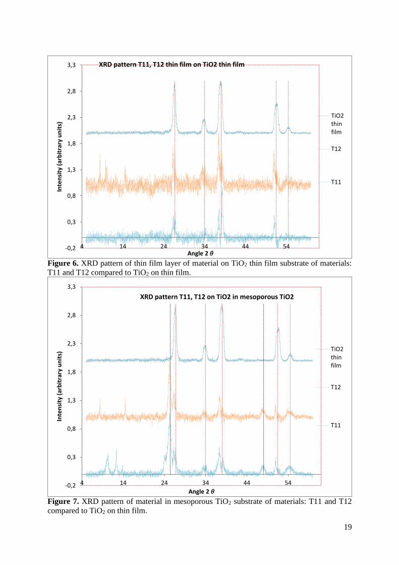
19
Figure 6. XRD pattern of thin film layer of material on TiO2 thin film substrate of materials:
T11 and T12 compared to TiO2 on thin film.
Figure 7. XRD pattern of material in mesoporous TiO2 substrate of materials: T11 and T12
compared to TiO2 on thin film.
-0,2
0,3
0,8
1,3
1,8
2,3
2,8
3,3
4 14 24 34 44 54
Inte
nsi
ty (
arb
itra
ry u
nit
s)
Angle 2 𝜃
XRD pattern T11, T12 thin film on TiO2 thin film
TiO2thinfilm
T12
T11
-0,2
0,3
0,8
1,3
1,8
2,3
2,8
3,3
4 14 24 34 44 54
Inte
nsi
ty (
arb
itra
ry u
nit
s)
Angle 2 𝜃
XRD pattern T11, T12 on TiO2 in mesoporous TiO2
TiO2thinfilm
T12
T11

20
Figure 8. XRD pattern of thin film layer of material on TiO2 thin film substrate of materials:
P1 and P2 compared to TiO2 on thin film
Figure 9. XRD pattern of material in mesoporous TiO2 substrate of materials: P1 and P2
compared to TiO2 on thin film.
-0,2
0,3
0,8
1,3
1,8
2,3
2,8
3,3
4 14 24 34 44 54
Inte
nsi
ty (
arb
itra
ry u
nit
s)
Angle 2 𝜃
XRD pattern P1, P2 thin film on TiO2 thin film
TiO2thinfilm
P2
P1
-0,2
0,3
0,8
1,3
1,8
2,3
2,8
3,3
4 14 24 34 44 54
Inte
nsi
ty (
arb
itra
ry u
nit
s)
Angle 2 𝜃
XRD pattern P1, P2 in mesoporous TiO2
TiO2thinfilm
P2
P1

21
Figure 10. XRD pattern of thin film layer of material on TiO2 thin film substrate of materials:
Cs1 and Cs2 compared to T3 and TiO2 on thin film.
Figure 11. XRD pattern of material in mesoporous TiO2 substrate of materials: Cs1 and Cs2
compared to T3 and TiO2 on thin film.
-0,2
0,3
0,8
1,3
1,8
2,3
2,8
3,3
3,8
4,3
4 14 24 34 44 54
Inte
nsi
ty (
arb
itra
ry u
nit
s)
Angle 2 𝜃
XRD pattern T3, Cs1, Cs2 thin film on TiO2 thin film
TiO2thinfilmCs2
Cs1
T3
-0,2
0,3
0,8
1,3
1,8
2,3
2,8
3,3
3,8
4,3
4 14 24 34 44 54
Inte
nsi
ty (
arb
itra
ry u
nit
s)
Angle 2 𝜃
XRD pattern T3, Cs1, Cs2 in mesoporous TiO2
TiO2thinfilmCs2
Cs1
T3
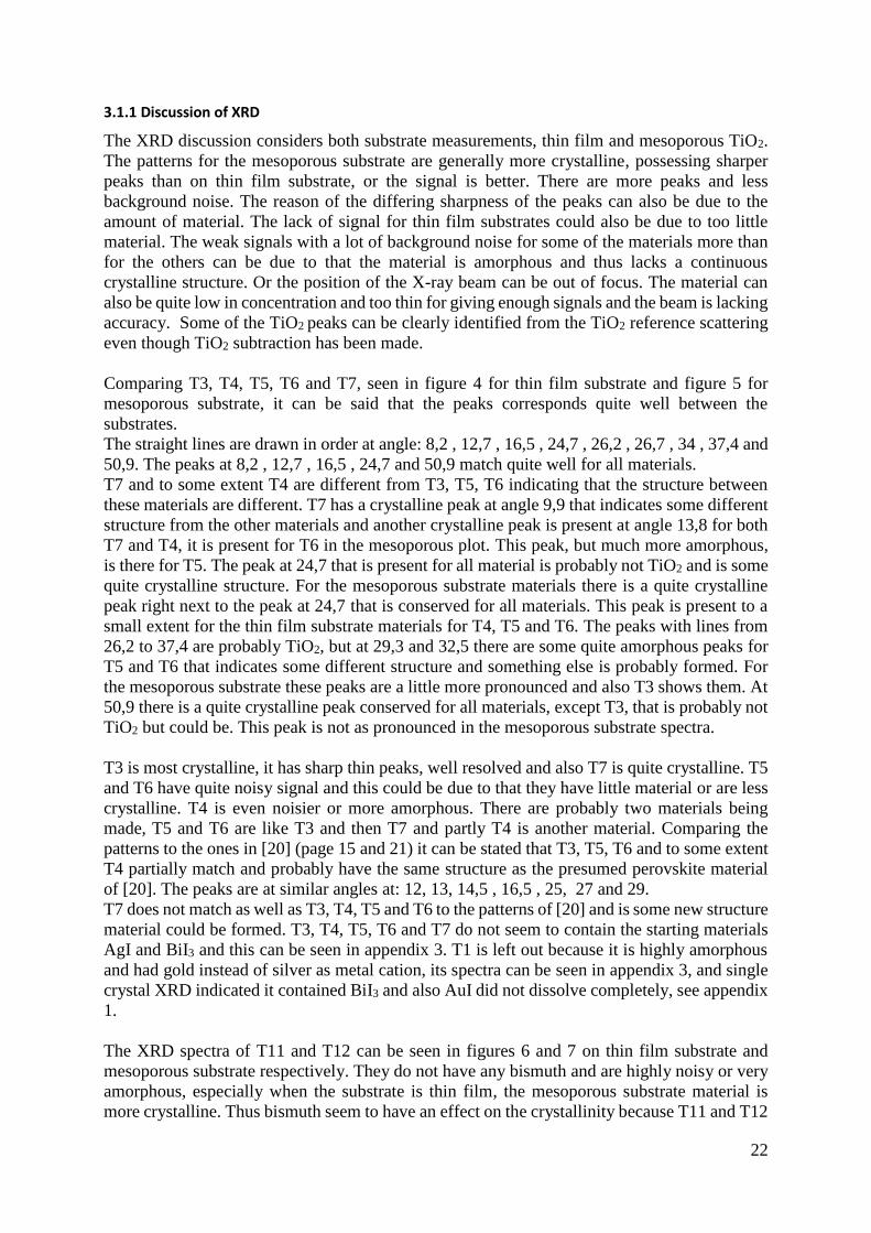
22
3.1.1 Discussion of XRD
The XRD discussion considers both substrate measurements, thin film and mesoporous TiO2.
The patterns for the mesoporous substrate are generally more crystalline, possessing sharper
peaks than on thin film substrate, or the signal is better. There are more peaks and less
background noise. The reason of the differing sharpness of the peaks can also be due to the
amount of material. The lack of signal for thin film substrates could also be due to too little
material. The weak signals with a lot of background noise for some of the materials more than
for the others can be due to that the material is amorphous and thus lacks a continuous
crystalline structure. Or the position of the X-ray beam can be out of focus. The material can
also be quite low in concentration and too thin for giving enough signals and the beam is lacking
accuracy. Some of the TiO2 peaks can be clearly identified from the TiO2 reference scattering
even though TiO2 subtraction has been made.
Comparing T3, T4, T5, T6 and T7, seen in figure 4 for thin film substrate and figure 5 for
mesoporous substrate, it can be said that the peaks corresponds quite well between the
substrates.
The straight lines are drawn in order at angle: 8,2 , 12,7 , 16,5 , 24,7 , 26,2 , 26,7 , 34 , 37,4 and
50,9. The peaks at 8,2 , 12,7 , 16,5 , 24,7 and 50,9 match quite well for all materials.
T7 and to some extent T4 are different from T3, T5, T6 indicating that the structure between
these materials are different. T7 has a crystalline peak at angle 9,9 that indicates some different
structure from the other materials and another crystalline peak is present at angle 13,8 for both
T7 and T4, it is present for T6 in the mesoporous plot. This peak, but much more amorphous,
is there for T5. The peak at 24,7 that is present for all material is probably not TiO2 and is some
quite crystalline structure. For the mesoporous substrate materials there is a quite crystalline
peak right next to the peak at 24,7 that is conserved for all materials. This peak is present to a
small extent for the thin film substrate materials for T4, T5 and T6. The peaks with lines from
26,2 to 37,4 are probably TiO2, but at 29,3 and 32,5 there are some quite amorphous peaks for
T5 and T6 that indicates some different structure and something else is probably formed. For
the mesoporous substrate these peaks are a little more pronounced and also T3 shows them. At
50,9 there is a quite crystalline peak conserved for all materials, except T3, that is probably not
TiO2 but could be. This peak is not as pronounced in the mesoporous substrate spectra.
T3 is most crystalline, it has sharp thin peaks, well resolved and also T7 is quite crystalline. T5
and T6 have quite noisy signal and this could be due to that they have little material or are less
crystalline. T4 is even noisier or more amorphous. There are probably two materials being
made, T5 and T6 are like T3 and then T7 and partly T4 is another material. Comparing the
patterns to the ones in [20] (page 15 and 21) it can be stated that T3, T5, T6 and to some extent
T4 partially match and probably have the same structure as the presumed perovskite material
of [20]. The peaks are at similar angles at: 12, 13, 14,5 , 16,5 , 25, 27 and 29.
T7 does not match as well as T3, T4, T5 and T6 to the patterns of [20] and is some new structure
material could be formed. T3, T4, T5, T6 and T7 do not seem to contain the starting materials
AgI and BiI3 and this can be seen in appendix 3. T1 is left out because it is highly amorphous
and had gold instead of silver as metal cation, its spectra can be seen in appendix 3, and single
crystal XRD indicated it contained BiI3 and also AuI did not dissolve completely, see appendix
1.
The XRD spectra of T11 and T12 can be seen in figures 6 and 7 on thin film substrate and
mesoporous substrate respectively. They do not have any bismuth and are highly noisy or very
amorphous, especially when the substrate is thin film, the mesoporous substrate material is
more crystalline. Thus bismuth seem to have an effect on the crystallinity because T11 and T12

23
had silver as metal cation by itself and they seem to lack a continuous crystalline pattern and
are highly amorphous. On thin film substrate T11 is very noisy and it is hard to distinguish any
other peaks than TiO2. The peaks for TiO2 are clearly distinguished for both substrates. T12 has
some low angle peaks at approximately 8,4 , 9,8 and 14,6 but they are not so crystalline. The
peak at 8,4 could perhaps be coupled to the peak at 8,2 of the materials with silver and bismuth
as metal cation. Neither T11 nor T12 seem to contain the pure reactants. For the mesoporous
substrate there are peaks for T11 at 10,4 and 12,3 and for T12 at 8,3 and 14,5. The peaks at 8,3
and 12,3 could perhaps be coupled to the silver and bismuth metal cation materials. The
different positions implies a difference in structure. At angle 25,4 for the mesoporous substrate
there is quite crystalline peaks for both T11 and T12 that is probably not TiO2, even though it
could be. This peak could be seen in T3-T7 materials at approximately 24,7-25,4. The peaks at
37,2 for both substrates is more probably TiO2. For the mesoporous substrate there are peaks at
angle 48,1 indicating some new structure but the peaks are quite amorphous. The peaks at 50,8
for both substrates and both T11 and T12 are most probably TiO2 but could also be something
else. Some similarities between T3-T7 and T11 and T12 are seen, with peaks matching and also
some differences indicating some new structure materials, even though T11 and T12 are more
amorphous.
P1 and P2 on thin film and mesoporous substrate can be seen in figures 8 and 9 respectively.
On both substrates and in particular on thin film and material P1, there seems to be quite much
background noise and the spectra are quite similar and they are not particularly crystalline,
except for P2 on mesoporous substrate that is quite crystalline. The peaks are mainly
corresponding to TiO2 even though subtraction has been made, red straight vertical lines
showing the TiO2 peaks. For the thin film substrate the peaks lying very close to the TiO2 peaks
are probably TiO2 but could possibly something else. For the mesoporous substrate these
closely lying peaks are more likely to be some other structure but could be TiO2 also. They are
more separated and slightly more crystalline. The peaks at 25,5 and 48,3 for the mesoporous
substrate probably indicates some new structure formed and these are present for the
mesoporous substrate for both P1 and P2. The difference between P1 and P2 is that P1 has gold
as cation and silver in P2. P2 has less background noise and more pronounced peaks probably
being more crystalline and the peak at 9,9 for P2, on both substrates, indicates something
crystalline present. This is not present in P1 indicating a difference in structure. P1 seem to
match with AuI to some extent, clearly at the peak at angle 13,2 and AuI is probably present
and this can be seen in appendix 3. AuI did probably not dissolve completely. P2 does not seem
to contain AgI.
Cs1 and Cs2 on thin film and mesoporous substrate, illustrated in figures 10 respectively 11.
Neither of the materials on none of the substrates contain the starting materials AgI, BiI3 nor
CsI and this can be seen in appendix 3.
The peaks for the spectra of Cs1 match to some extent with the spectra in [20] for the same
presumed material and the structure could possibly be assigned to Cs3Bi2I9. Comparing T3 with
methylammonium as cation to Cs1 with cesium as cation the peaks are placed at the same angles
but slightly shifted for Cs1 indicating the approximately the same structure and the slight shift
indicates the difference in cation size that has some effect on structure. The shifts also tend to
increase with increasing angle. These shifts are observed in [20] even though the comparison
might not be optimal in this project, since the methylammonium cation material differs in metal
cation and amount and stoichiometry of cation. The structure of Cs1 and Cs2 are very similar,
though the peaks are slightly differently placed thus indicating some difference. For Cs2 the
peaks are slightly less pronounced and sharp in comparison to Cs1 indicating that Cs2 is more
amorphous. Though some of the peaks match [20] and the pattern is a little similar and the
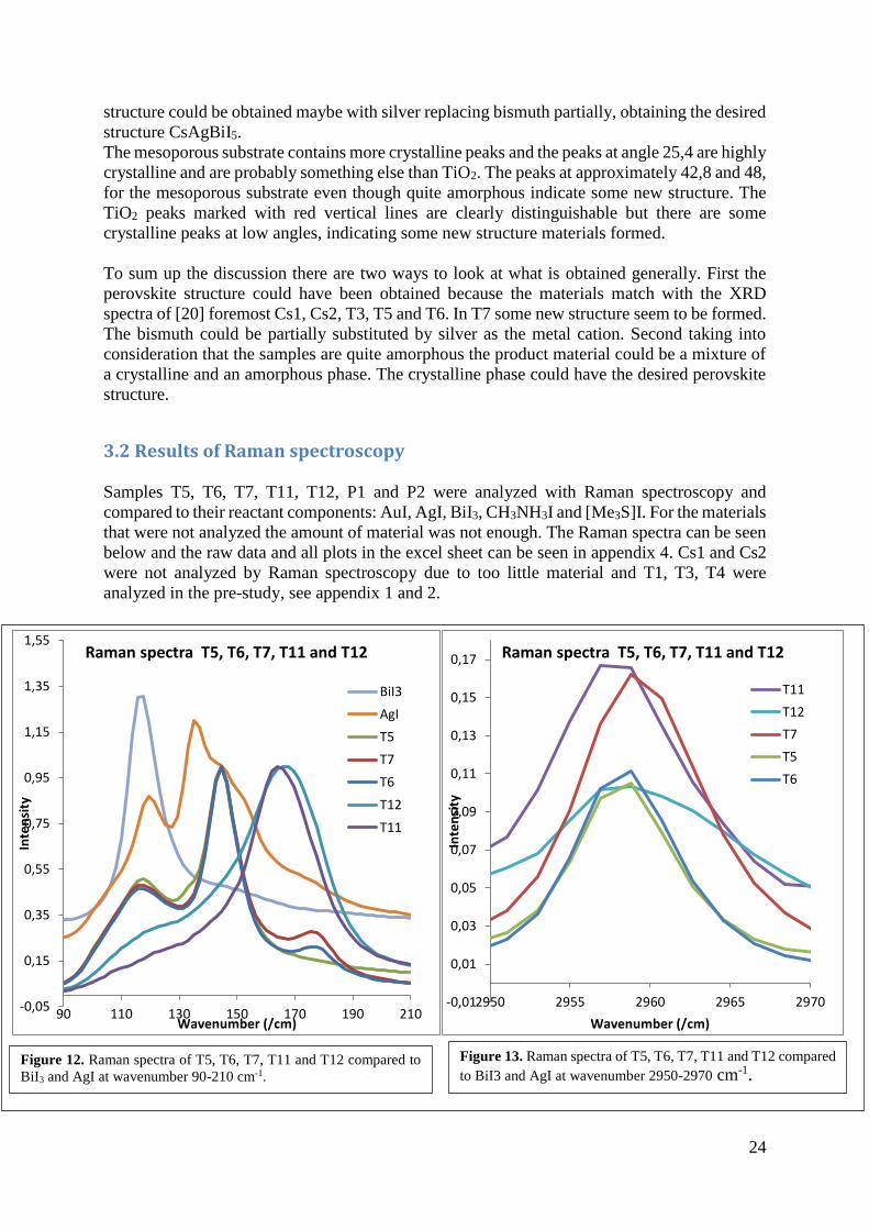
24
structure could be obtained maybe with silver replacing bismuth partially, obtaining the desired
structure CsAgBiI5.
The mesoporous substrate contains more crystalline peaks and the peaks at angle 25,4 are highly
crystalline and are probably something else than TiO2. The peaks at approximately 42,8 and 48,
for the mesoporous substrate even though quite amorphous indicate some new structure. The
TiO2 peaks marked with red vertical lines are clearly distinguishable but there are some
crystalline peaks at low angles, indicating some new structure materials formed.
To sum up the discussion there are two ways to look at what is obtained generally. First the
perovskite structure could have been obtained because the materials match with the XRD
spectra of [20] foremost Cs1, Cs2, T3, T5 and T6. In T7 some new structure seem to be formed.
The bismuth could be partially substituted by silver as the metal cation. Second taking into
consideration that the samples are quite amorphous the product material could be a mixture of
a crystalline and an amorphous phase. The crystalline phase could have the desired perovskite
structure.
3.2 Results of Raman spectroscopy
Samples T5, T6, T7, T11, T12, P1 and P2 were analyzed with Raman spectroscopy and
compared to their reactant components: AuI, AgI, BiI3, CH3NH3I and [Me3S]I. For the materials
that were not analyzed the amount of material was not enough. The Raman spectra can be seen
below and the raw data and all plots in the excel sheet can be seen in appendix 4. Cs1 and Cs2
were not analyzed by Raman spectroscopy due to too little material and T1, T3, T4 were
analyzed in the pre-study, see appendix 1 and 2.
-0,05
0,15
0,35
0,55
0,75
0,95
1,15
1,35
1,55
90 110 130 150 170 190 210
Inte
nsi
ty
Wavenumber (/cm)
Raman spectra T5, T6, T7, T11 and T12
BiI3
AgI
T5
T7
T6
T12
T11
-0,01
0,01
0,03
0,05
0,07
0,09
0,11
0,13
0,15
0,17
2950 2955 2960 2965 2970
Inte
nsi
ty
Wavenumber (/cm)
Raman spectra T5, T6, T7, T11 and T12
T11
T12
T7
T5
T6
Figure 12. Raman spectra of T5, T6, T7, T11 and T12 compared to
BiI3 and AgI at wavenumber 90-210 cm-1.
Figure 13. Raman spectra of T5, T6, T7, T11 and T12 compared
to BiI3 and AgI at wavenumber 2950-2970 cm-1.

25
3.2.1 Discussion of Raman spectroscopy
For the materials two major areas of peaks are present, one at approximately 100-180 and the
other, just below 3000 cm-1.
Figure 12 shows the first peak areas for T5, T6, T7, T11 and T12 where the first peak at 117
cm-1 seem to be correspond to bismuth and the peak at 144 cm-1 is probably silver. For T11 and
T12 the first peak indicates no bismuth present as they do not contain it. The silver reference
material have not a Gaussian form which is the form for one vibrational bond and this indicates
that the reference material have many different bond lengths. It can be interpreted that there
probably has been some new bonds formed in the synthesis because the silver peaks of the
materials does not match precisely with that of AgI. The intensity of the peaks could be
correlated to the stoichiometry and thus it is probably more silver present than bismuth. For T6
there is an additional peak at 177 cm-1 and it indicates that something new is formed. For T7
the peak at 177 cm-1 increases in intensity compared to T6 and the new bond and structure is
probably more present and in a higher amount. More methylamine seem to give some new bond
and probably also a new structure. A new vibration is the cause of a new bond and might be a
new structure formed. For T5, T6 and T7 the bismuth and silver bonds are present at 117 cm-1
respectively 144 cm-1. The bismuth bond at 117 cm-1 is most pronounced for T5, then T7 and
then T6 and this indicates no trend. The silver peak at 144 cm-1 is equal for the samples. For
T11 there is some silver vibration but it is another wavenumber and thus another bond or
structure. Something other than the reactants are most probably formed. The low energy
vibration at 163 cm-1 shifts slightly to the right for T12 compared to T11 indicating shorter bond
distances and possibly a new structure material. There is also indication of more peaks at
approximately 120 cm-1 and thus more bonds for T12 indicating that something new is formed
probably out of silver. The peak from T11 also grows slightly when the methylamine is
increased in T12.
-0,1
0,1
0,3
0,5
0,7
0,9
1,1
1,3
90 110 130 150 170 190 210
Inte
nsi
ty
Wavenumber (/cm)
Raman spectra P1 and P2 AuI
(Me3S)I
AgI
P2
P1
-0,1
0,1
0,3
0,5
0,7
0,9
1,1
2870 2920 2970 3020In
ten
sity
Wavenumber (/cm)
Raman spectra P1 and P2
AuI
(Me3S)I
P1
AgI
P2
Figure 14. Raman spectra of P1 and P2 compared to AuI, AgI and
[Me3S]I at wavenumber 90-210 cm-1.
Figure 15. Raman spectra of P1 and P2 compared to AuI, AgI and
[Me3S]I at wavenumber 2870-3030 cm-1.

26
Looking at figure 13 that shows the organic vibration bond at approximately 2960 cm-1, that
indicates a C-H bond and the reference material CH3NH3I has its peak here and all the material
also have their peaks at approximately this wavenumber but the intensities are much lower.
CH3NH3I is left out of the figure because it is 4,8-8,1 times higher in intensity compared to the
materials, but can be seen in appendix 4. Usually the organic bond at this wavenumber is
relatively intensive and the low intensity might indicate that there is not so much organic cation
present in the product. The organic cation usually does not change in perovskites compared to
the organic reference material since the organic cation is just electrostatically connected to the
anion in the perovskite structure. This has previously been stated in studies of organic lead
halide perovskites. The organic cation could possibly be coordinated in another way but this
will not give fluctuation for the Raman spectra. If the organic cation is present that is an
indication of that there is an anion in the product because methylamine is positively charged
and needs to be balanced in the neutral product. Thus if the reactants forming the anion are not
present in their original form and the organic bond is occurring, some new material could have
been formed. There is peak at around 3000 cm-1 for AgI and it is most likely not the material
itself but rather a sign of water present, this can be seen in appendix 4.
The intensity of organic stretch at 2960 cm-1 is highest for T11 followed by T7. Then T6, T5
and T12 have approximately the same intensities, slightly smaller than the other two. The
matching of T6 to CH3NH3I is slightly more pronounced than for T5, for example the CH3
vibration just below 1500 cm-1, that can be seen in appendix 4.
The matching for T7 to CH3NH3I is more than for both T5 and T6 indicating that the product
more probably consists of the organic cation and thus an anion and because of this it is more
probable that the silver and bismuth have formed the octahedron with iodine. The probability
of having a more desirable product is also strengthened by the increasing intensity of the new
energy bond occurring in T6 and more pronounced in T7 at 177 cm-1. The probable product
could have been obtained. The organic bond at 2957 cm-1 is more pronounced for T11 than T12
indicating more probability of having an organic cation and a desired anion in the product.
In summary, comparing materials T5, T6, T7, T11 and T12, it can be noted that the probable
silver stretch shifts to the right for T11 and T12 and this might be an indication for some new
structure forming. New structures are most likely formed for T5, T6 and T7 with increasing
tendency with T7 most probably having another structure because of new vibrations. T11 and
T7 seem to have most tendency to form the organic cation that is beneficial for the desired anion
to form and thus the perovskite structure. The pure reactants are not recrystallized.
The low wavenumber vibrations for P1 and P2 can be seen in figure 14. For P1 there is a little
starting material in the beginning matching the peaks of AuI at 127 and 143 cm-1, but the peaks
for the material are slightly shifted and this might indicate some new bond of gold, but
recrystallization of the reactants, at least to some extent, cannot be excluded. Then something
new is formed in the big peak at 180 cm-1, but it is unclear what. For P2 the peak position for
silver is not conserved and there is probably a new structure formed. The new silver bond is
perhaps the vibration at 167 cm-1.
From figure 15 it can be seen that organic stretches corresponding to trimethylsulfonium iodide,
at approximately 2910 and 2995 cm-1, are present for P2 but absent for P1. The absence of
cation trimethylsulfonium for P1 decreases the probability of having the desired product as the
reactants might have been recrystallized even though the peak at 180 cm-1 indicates something

27
new has formed for P1 and the gold peaks are shifted slightly. The constant signal at 3000 cm-
1 is probably just noise and the Raman analyze should preferably be redone for P1.
For P2 the trimethylsulfoniumiodide is present because it matches very well with the material
at the organic stretches at around 2910 and 2995 cm-1. This is also the case at 1400 cm-1, seen
in appendix 4. In the case of P2, to have the organic cation in the product as well as a peak
position shift for silver is enabling the formation of a desired product at least something else
than the reactants recrystallization. Gold and silver are not relevant to compare to each other
but probably some new structures with these elements are formed for each case, P1 and P2.
3.3 Results of solar cell performance
Solar cells were made with two different HTMs Spiro-OMeTAD and Sulphur polymer.
T3, T5, Cs1 and Cs2 were made with Spiro-OMeTAD. T1, T3, T4, T5, T6, T7, T11, T12, P1,
P2, Cs1 and Cs2 were assembled with Sulphur polymer.
For all the materials there is a table of short circuit current, open circuit voltage, fill factor and
efficiency for the best performing solar cell and an average of the 8-12 cells tested. Also
standard deviation and variance are given. There is also a J-V plot for all materials with the best
performing cells curve. Histograms for each solar cell material are also given. The solar cells
with Sulphur polymer did not work as well as those with Spiro-OMeTAD and a large part of
them did not show diode behavior, those are not included in the J-V plots. For this reason no
histograms were made for the solar cells with Sulphur polymer HTM. The complete data and
all plots can be found in appendixes 5 and 6.
3.3.1 Results of solar cells with Spiro-OMeTAD as HTM
The area was 0,126 cm2 and the scan rate 50 mV/s. The color of T3 was orange red, T5 was
orange red, Cs1 was pale red and Cs2 was pale orange. The J-V curves for T3, T5, Cs1 and Cs2
are seen in figure 16 and the histograms in figures 17 and 18. Table 5 summarizes the
performance of the cells.
Figure 16. J-V curves for T3, T5, Cs1 and Cs2.
0
0,01
0,02
0,03
0,04
0,05
0,06
0,07
0,08
0,09
0,1
0 0,1 0,2 0,3 0,4 0,5
J (m
A/c
m^2
V (V)
JV-curves T3, T5, Cs1 and Cs2. (Spiro-OMeTAD)
T5
Cs2
T3
Cs1
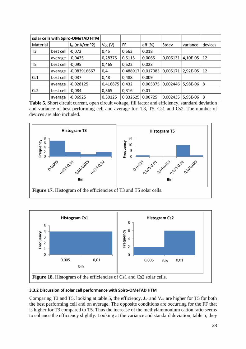
28
solar cells with Spiro-OMeTAD HTM
Material Jsc (mA/cm^2) VOC (V) FF eff (%) Stdev variance devices
T3 best cell -0,072 0,45 0,563 0,018
average -0,0435 0,28375 0,5115 0,0065 0,006131 4,10E-05 12
T5 best cell -0,095 0,465 0,522 0,023
average -0,083916667 0,4 0,488917 0,017083 0,005171 2,92E-05 12
Cs1 best cell -0,037 0,48 0,488 0,009
average -0,028125 0,416875 0,432 0,005375 0,002446 5,98E-06 8
Cs2 best cell -0,084 0,365 0,316 0,01
average -0,06925 0,30125 0,332625 0,00725 0,002435 5,93E-06 8
Table 5. Short circuit current, open circuit voltage, fill factor and efficiency, standard deviation
and variance of best performing cell and average for: T3, T5, Cs1 and Cs2. The number of
devices are also included.
3.3.2 Discussion of solar cell performance with Spiro-OMeTAD HTM
Comparing T3 and T5, looking at table 5, the efficiency, Jsc and Voc are higher for T5 for both
the best performing cell and on average. The opposite conditions are occurring for the FF that
is higher for T3 compared to T5. Thus the increase of the methylammonium cation ratio seems
to enhance the efficiency slightly. Looking at the variance and standard deviation, table 5, they
Figure 17. Histogram of the efficiencies of T3 and T5 solar cells.
02468
Fre
qu
en
cy
Bin
Histogram T3
0
5
10
15
Fre
qu
en
cy
Bin
Histogram T5
Figure 18. Histogram of the efficiencies of Cs1 and Cs2 solar cells.
0
1
2
3
4
5
0,005 0,01
Fre
qu
en
cy
Bin
Histogram Cs1
0
2
4
6
8
0,005 0,01
Fre
qu
en
cy
Bin
Histogram Cs2

29
are slightly lower for T5 indicating the values are more close to each other and smaller error
and this is also strengthened by the histograms, in figure 17, where the data is more gathered
for T5. But the values are very low and are probably not so reliable but at least gives some
guidelines for the relationships.
Looking at table 5, Cs2 has slightly higher efficiency than Cs1 but lower fill factor, for the best
performing cell and on average. The open circuit voltage is higher for Cs1 for both best
performing cell and on average. The Jsc is higher for Cs2 for both best performing cell and on
average. The materials were similarly pale but Cs1 was redder and Cs2 more orange and they
were both half transparent. The efficiency is marginally higher when silver and bismuth are the
metallic cation instead of bismuth alone. For Cs1 and Cs2 the variance and standard deviation
are almost equal, slightly lower and thus better for Cs2, the values are relatively small. The
histogram, seen in figure 18, shows that Cs1 is more symmetric indicating more even data.
Looking at T3 and T5 versus Cs1 and Cs2 it seems that the methylammonium cation gives a
higher efficiency than cesium. The FF is also higher for T3 and T5. The variance and standard
deviations are smaller for Cs1 and Cs2 compared to T3 and T5 but it has to be taken into
consideration that 12 devices are tested for T3 and T5 and 8 devices for Cs1 and Cs2 and this
contributes to these statistical parameters. The histograms are also more symmetrical and thee
data more gathered for Cs1 and Cs2 compared to T3 and T5.
Considering the previously done study [20] on bismuth perovskites, it gave the cesium cation
solar cells performing better than the methylammonium ones. The methylammonium had
bismuth as the only metal cation and thus it might not be optimally comparable with this study
that had, either silver and bismuth, or silver alone. In this study the methylammonium solar
cells had higher efficiencies than the cesium ones. The efficiency was for Cs3Bi2I9 1,09% in
[20] to compare with the presumed same structured material Cs1of this study that had an
efficiency of 0,009 % for the best performing cells. The cesium material Cs2 with silver and
bismuth as metal cations gave 0,01% for the best performing cell. The CH3NH3Bi2I9 in [20]
had an efficiency of 0,12 % while the methylammonium silver bismuth iodides of this study
had efficiencies of 0,018 and 0,023 %.
The efficiencies of this study were much lower and this might be due to the manufacturing
process. The glasses were not perfectly cut. This probably result in misalignment of the silver
layer and FTO and thus the functioning of the cells. The scan rate differed and this can be an
explanation to the low efficiency.
3.3.3 Results of solar cells with Sulphur polymer as HTM
Below is the materials that were made to solar cells, 7-8 devices of each material with Sulphur
polymer as HTM. The devices that showed an ohmic diode behavior are shown in the report,
the rest can be viewed in appendix 5. The area was 0,126 cm2 and the scan rate 22,7 mV/s. The
data of solar cells: T1, T4, T11, T12, P1 and P2 did not show ohms law for diodes.

30
solar cells with Sulphur polymer HTM
Material Jsc (mA/cm^2) Voc (V) FF eff (%) Stdev variance devices
T3 best cell 0,0569 0,075 2,35E-01 1,00E-05
average 0,049523 0,049375 2,49E-01 5,83E-06 3,10E-06 9,40E-12 4
T5 best cell 0,20322 0,079 2,70E-01 4,33E-05
average 1,89E-01 0,039667 2,89E-01 2,18E-05 1,90E-05 3,60E-10 3
T6 best cell 0,308 0,065 3,30E-01 6,60E-05
average 0,21195 0,070875 3,70E-01 4,85E-05 1,10E-05 1,20E-10 8
T7 best cell 1,27E-01 0,055 2,85E-01 1,99E-05
average 1,31E-01 0,036 2,66E-01 1,29E-05 6,60E-06 4,40E-11 7
Cs1 best cell 0,0096058 0,195 1,88E-01 3,52E-06
average 0,00625295 0,12 2,37E-01 1,73E-06 1,20E-06 1,50E-12 4
Cs2 best cell 0,014 0,07 2,32E-01 2,27E-06
average 0,0096 0,06 2,53E-01 1,49E-06 7,20E-07 5,20E-13 4
Table 6. Short circuit current, open circuit voltage, fill factor and efficiency for T3, T5, T6,
T7, Cs1 and Cs2 best performing cell and average of the cells showing diode behavior. Also
standard deviation, variance and number of devices are given.
Figure 19. J-V curve of best performing cell for T3, T5, T6, T7, Cs1 and Cs2.
0
0,05
0,1
0,15
0,2
0,25
0,3
0,35
0 0,01 0,02 0,03 0,04 0,05 0,06 0,07 0,08
J (m
A/c
m^2
V (V)
J-V curves T3, T5, T6, T7, Cs1 and Cs2. (Sulphur polymer)
T6
T5
T7
T3
Cs2
Cs1

31
3.3.4 Pictures of solar cells with Sulphur polymer HTM
3.3.5 Discussion of solar cell performance with Sulphur polymer HTM
The chlorobenzene was not completely dry and might have affected that the material changed
color after the addition of HTM. The cation could be dissolved by a slightly wet chlorobenzene.
The colors of the solar cells can be viewed under the heading “Pictures of solar cells with
Sulphur polymer HTM”, in figure 20. Cells T1, T4, T11, T12, P1 and P2 got almost completely
transparent after spin coating of the Sulphur polymer HTM. The other materials got paler but
they are not completely transparent. This is a very probable reason for the low function in solar
cells.
Some of the materials had completely ohmic metal behavior and all of the materials had it to
some extent. T1, T4, T11, T12, P1 and P2 were completely ohmic metallic and they were also
the ones that were transparent. It is possible that no material was there and thus the contacts
were measured. The rest of the materials had partly ohmic metallic behavior but considered
enough diode to be presentable. The reason for the ohmic metal behavior in these materials, is
probably wrong coupling of the devices so that the FTO layer is dis-functioned. By doing J-V
measurements on silver and FTO solely it was examined if the metallic behavior of the solar
cells could be coupled to these materials. The conductivity of the solar cells turned out to be in
between the one for silver and the one for FTO, where silver has higher conductivity. This can
be seen in appendix 7. The probable reason for this is that it is the contacts that are measured
and that silver is residing on FTO. The etching is also a probable source to the lack of ohmic
diode characteristics, because of that the recombination is then substantial. Without the FTO
layer the current path does not become the intended and the current goes in the direction that is
most energetically beneficial. This leads to that the silver is the part measured and not the rest
of the solar cell.
T1 T3 T4 T5 T6 T7
T11 T12 P1 P2 Cs1 Cs2
Fig 20. Solar cells of materials T1, T3, T4, T5, T6, T7, T11, T12, P1, P2,
Cs1 and Cs2 with Sulphur polymer HTM.
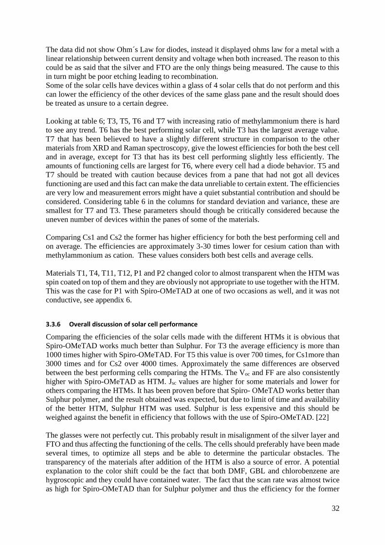
32
The data did not show Ohm´s Law for diodes, instead it displayed ohms law for a metal with a
linear relationship between current density and voltage when both increased. The reason to this
could be as said that the silver and FTO are the only things being measured. The cause to this
in turn might be poor etching leading to recombination. Some of the solar cells have devices within a glass of 4 solar cells that do not perform and this
can lower the efficiency of the other devices of the same glass pane and the result should does
be treated as unsure to a certain degree.
Looking at table 6; T3, T5, T6 and T7 with increasing ratio of methylammonium there is hard
to see any trend. T6 has the best performing solar cell, while T3 has the largest average value.
T7 that has been believed to have a slightly different structure in comparison to the other
materials from XRD and Raman spectroscopy, give the lowest efficiencies for both the best cell
and in average, except for T3 that has its best cell performing slightly less efficiently. The
amounts of functioning cells are largest for T6, where every cell had a diode behavior. T5 and
T7 should be treated with caution because devices from a pane that had not got all devices
functioning are used and this fact can make the data unreliable to certain extent. The efficiencies
are very low and measurement errors might have a quiet substantial contribution and should be
considered. Considering table 6 in the columns for standard deviation and variance, these are
smallest for T7 and T3. These parameters should though be critically considered because the
uneven number of devices within the panes of some of the materials.
Comparing Cs1 and Cs2 the former has higher efficiency for both the best performing cell and
on average. The efficiencies are approximately 3-30 times lower for cesium cation than with
methylammonium as cation. These values considers both best cells and average cells.
Materials T1, T4, T11, T12, P1 and P2 changed color to almost transparent when the HTM was
spin coated on top of them and they are obviously not appropriate to use together with the HTM.
This was the case for P1 with Spiro-OMeTAD at one of two occasions as well, and it was not
conductive, see appendix 6.
3.3.6 Overall discussion of solar cell performance
Comparing the efficiencies of the solar cells made with the different HTMs it is obvious that
Spiro-OMeTAD works much better than Sulphur. For T3 the average efficiency is more than
1000 times higher with Spiro-OMeTAD. For T5 this value is over 700 times, for Cs1more than
3000 times and for Cs2 over 4000 times. Approximately the same differences are observed
between the best performing cells comparing the HTMs. The Voc and FF are also consistently
higher with Spiro-OMeTAD as HTM. Jsc values are higher for some materials and lower for
others comparing the HTMs. It has been proven before that Spiro- OMeTAD works better than
Sulphur polymer, and the result obtained was expected, but due to limit of time and availability
of the better HTM, Sulphur HTM was used. Sulphur is less expensive and this should be
weighed against the benefit in efficiency that follows with the use of Spiro-OMeTAD. [22]
The glasses were not perfectly cut. This probably result in misalignment of the silver layer and
FTO and thus affecting the functioning of the cells. The cells should preferably have been made
several times, to optimize all steps and be able to determine the particular obstacles. The
transparency of the materials after addition of the HTM is also a source of error. A potential
explanation to the color shift could be the fact that both DMF, GBL and chlorobenzene are
hygroscopic and they could have contained water. The fact that the scan rate was almost twice
as high for Spiro-OMeTAD than for Sulphur polymer and thus the efficiency for the former

33
solar cells should be lower than for the latter relatively, (350-2000 times higher for Spiro-
OMeTAD instead approximately, depending on how much the scan rate is believed to affect).
3.4 Result of conductivity measurements and calculation
Two conductivity tests were done, first on the material P1 tested in solar cells in the pre-study
and second on the nine materials: T3, T4, T5, T6, T7, T11, T12, P1 and P2. The materials left
out that were T1, Cs1 and Cs2 had too little material to perform the test on.
The first conductivity test of P1 material gave 0 conductivity. The data was highly scattered
and gave no reliable trendline, and it is probable that the data is only background scattering
because the material might have disappeared. For calculations and plot see appendix 7.
For the second round of conductivity tests the material P1 proved to have quite good
conductivity as well as the rest of the materials. The conductivities and standard deviation and
variance are plotted in table 7 and the best conductivity plot of each material is found in figure
21. The complete data and all plots are found in appendix 8.
Material average conductivity (s/cm) Stdev Variance nr of devices
T3 8,11E-06 3,51E-06 1,23E-11 3
T4 1,67E-06 4,19E-07 1,76E-13 6
T5 1,37E-05 3,72E-06 1,39E-11 6
T6 1,52E-05 1,10E-05 1,20E-10 3
T7 9,12E-05 - - 1
T11 6,08E-06 0,00E+00 0,00E+00 6
T12 1,06E-04 1,66E-05 2,77E-10 6
P1 2,99E-04 1,24E-05 1,54E-10 6
P2 5,57E-07 2,89E-07 5,24E-14 6
Table 7. Table of the average conductivity, standard deviation, variance and number of devices
tested for each material.
Figure 21. Best conductivity J-V plot for T3, T4, T5, T6, T7, T11, T12, P1 and P2, also the
trendline is shown.
T3: y = 4E-09xT4: y = 8E-10x
T5: y = 6E-09xT6: y = 9E-09x
T7: y = 3E-08x
T11: y = 2E-09x
T12: y = 4E-08x
P1: y = 1E-07xP2: y = 3E-09x
-1,20E-07
-7,00E-08
-2,00E-08
3,00E-08
8,00E-08
1,30E-07
-1,05E+00 -5,50E-01 -5,00E-02 4,50E-01 9,50E-01
Cu
rre
nt
A/c
m2
V( V)
J-V curves T3, T4, T5, T6, T7, T11, T12, P1, P2
T3
T4
T5
T6
T7
T11
T12
P1
P2

34
3.4.1 Discussion of conductivity measurement and calculation
For P1 the material was probably destroyed when performing the first set of conductivity
measurements. The data is scattered indicating no trend, so probably it is background scattering
that is obtained. So there is no conductivity even though the calculation gives a quite good value
for it, see appendix 7. Excel makes a linear interpolation which is incorrect because it does not
take into account all values. The color was very light and the J-V curves obtained were not
linear as expected but constantly fluctuating. It was strange that the material did not become
liquid at 140°C because it was when synthesized. Some degradation process might be the cause
to this. If the perovskite material was present on top of the TiO2 mesoporous layer during the
conductivity test could be investigated through XRD on the conduction material compared to
XRD of the [Me3S]2[AuI4][I3] material itself. The solvent could be the cause to the potential
destruction of the material.
The second conductivity test gave more promising results. P1 gave the highest conductivity and
the conductivity was quite high, almost three times higher than for methylammonium lead
iodide that has a conductivity of 1,1x10⁻⁴ s/cm [3]. Also T12 gave a relatively high conductivity,
slightly lower than methylammonium lead iodide. From figure 21 it can be seen that P1 has the
greatest slope giving the highest conductivity, followed by T12. Increasing the amount of
methylammonium resulted in slightly higher conductivity, seen if looking at T3, T5, T6 and
T7. Comparing T11 and T12, that have silver as the sole metal cation, the conductivity is higher
for T12 and also here an increase of the methylammonium ratio increases the conductivity.
Comparing P1 and P2, a change of gold to silver gives a drastic decrease in conductivity.
Considering the uncertainties, T11 gave the same result at all measurements and should be
reliable. T7 was only measured one time due to the little amount of material and also T6 and
T3 does not have as many measurements as the other materials. P2 has the smallest difference
between the measurement looking at the values for standard deviation and variance. The smaller
value for standard deviation and variance the higher certainty of the measurements. The values
for these parameters can be seen in table 7.

35
3.5 Result of UV-vis absorption measurements and calculation
Below are the results for the UV-vis absorption measurements and estimated bandgaps. The
complete excel sheets are found in appendix 9.
Fig 22. Absorption spectra without TiO2 corrected of materials: T3, T4, T5, T6,
T7, T11, T12, P1, P2, Cs1 and Cs2.
Fig 23. Absorption spectra with TiO2 corrected of materials: T3, T4, T5, T6,
T7, T11, T12, P1, P2, Cs1 and Cs2.
0
0,5
1
1,5
2
2,5
300 400 500 600 700 800
Ab
sorb
ance
Wavelength (nm)
Absorption spectra of T3, T4, T5, T6, T7, T11, T12, P1, P2, Cs1 and Cs2. Without TiO2 corrected
T5
T6
T3
T7
Cs2
P1
Cs1
T4
T11
P2
T12
0
0,1
0,2
0,3
0,4
0,5
0,6
0,7
0,8
0,9
1
400 450 500 550 600 650 700 750 800
Ab
sorb
ance
Wavelength (nm)
Absorption spectra of T3, T4, T5, T6, T7, T11, T12, P1, P2, Cs1 and Cs2. TiO2 corected
T7
T3
T5
T6
Cs1
P1
Cs2
T4
T12
P2
T11
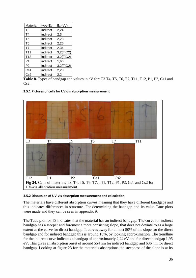
36
Material type Eg Eg (eV)
T3 indirect 2,24
T4 indirect 2,3
T5 indirect 2,23
T6 indirect 2,26
T7 indirect 2,34
T11 indirect 3,2(TiO2)
T12 indirect 3,2(TiO2)
P1 indirect 1,66
P2 indirect 3,2(TiO2)
Cs1 indirect 2,28
Cs2 indirect 2,2
Table 8. Types of bandgap and values in eV for: T3 T4, T5, T6, T7, T11, T12, P1, P2, Cs1 and
Cs2.
3.5.1 Pictures of cells for UV-vis absorption measurement
3.5.2 Discussion of UV-vis absorption measurement and calculation
The materials have different absorption curves meaning that they have different bandgaps and
this indicates differences in structure. For determining the bandgap and its value Tauc plots
were made and they can be seen in appendix 9.
The Tauc plot for T3 indicates that the material has an indirect bandgap. The curve for indirect
bandgap has a steeper and foremost a more consisting slope, that does not deviate to as a large
extent as the curve for direct bandgap. It curves away for almost 50% of the slope for the direct
bandgap and for indirect bandgap this is around 10%, by looking approximation. The trendline
for the indirect curve indicates a bandgap of approximately 2,24 eV and for direct bandgap 1,95
eV. This gives an absorption onset of around 554 nm for indirect bandgap and 636 nm for direct
bandgap. Looking at figure 23 for the materials absorptions the steepness of the slope is at its
T3 T4 T5 T6 T7 T11
T12 P1 P2 Cs1 Cs2
Fig 24. Cells of materials T3, T4, T5, T6, T7, T11, T12, P1, P2, Cs1 and Cs2 for
UV-vis absorption measurement.

37
greatest at 554 nm and relatively flat at 636 nm, further strengthening the hypothesis that the
material possesses an indirect bandgap.
Tauc plot of T4 shows that the trendlines match relatively well with the curve for both indirect
and direct bandgap. The slope for indirect bandgap is though greater. The extrapolation gives a
bandgap for indirect bandgap of 2,30 and direct 2,06. Converting it to absorption wavelength it
becomes 539 and 602 respectively. Looking at figure 23 with the absorption spectra there is no
absorption at 602 nm, the curve is completely flat there, while there is absorption at 539 nm,
indicating that the bandgap is indirect.
In the Tauc plot for T5 the slope for the indirect bandgap trendline is steeper and also matches
more with the curve than is the case for the direct bandgap. Approximately half of it bends away
and for the indirect bandgap this is around 10%. The bandgap for the indirect bandgap curve is
calculated to 2,23 eV and for the direct 1,93 by extrapolation. For the absorption wavelength
for indirect and direct curves this corresponds to 556 nm and 642 nm respectively. Looking at
figure 23 the curve is starting to steepen at 556 nm while it is quite flat at 642 nm. The bandgap
of the material is thus probably indirect considering these facts.
In the Tauc plot for T6 it is seen that the trendline for indirect bandgap matches the curve better
than is the case for the direct bandgap. The slope is also steeper for the indirect bandgap
trendline and this indicates an indirect bandgap. This is strengthened by taking out the bandgap
values by extrapolation, for the indirect bandgap 2,26 and for direct 2,05 and converting it to
absorption wavelength and looking at the absorption spectra in figure 23. The slope for the
absorption for T6 is starting to steepen at approximately 549 nm and the curve is quite flat at
605 nm. The bandgap is thus indirect.
For T7 the trendline for the indirect bandgap matches better, approximately 10% curves of, and
the trendline is steeper in comparison to the direct bandgap curve. By determining the bandgap
which is 2,34 for the indirect bandgap and 2,07 for direct, the absorption wavelength is
calculated to 530 for indirect and 599 for direct bandgap. The plot of the absorption to
wavelength in figure 23, indicates that the bandgap is indirect because the slope increases
steeply in at 530 nm wavelength and is relatively flat at 599 nm.
The Tauc plot for T11 clearly indicates the behavior of TiO2 and it is probably present at the
surface of the cells. The bandgap is around 3,2[24] (seen in figure 22 showing the absorptions
without TiO2 subtracted, absorption occurring at around 390 nm) which is the approximate
bandgap of titanium. The absorption curves for T12 and P2 coincides quite well with the one
for T11 indicating that all these materials have titanium absorption and the material if it is
present at all(the color was very pale for all these three and all the cells can be seen in figure
24) does not absorb light. Figure 23 shows the absorption spectra after correction of TiO2 and
shows no absorption for T12 and P2. T11 is not seen because it was assumed to have purely
titanium and was used as reference material.
The Tauc plot for P1 shows that the slope of the trendline for the direct bandgap is steeper than
the indirect one, the consistency with curve is thus slightly better for the indirect bandgap
trendline. The bandgaps given by extrapolation becomes for indirect bandgap 1,66 eV and for
direct 1,47eV. This gives an absorption wavelength of 747 nm and 844 nm respectively. The
measurement starts from a wavelength of 800 nm and the curves are all flat at this point. The
absorption for P1 thus starts at approximately a wavelength of 747 nm strengthened by the fact

38
that the material is black and should have absorption at this point. Thus the bandgap is probably
indirect for P1.
In the Tauc plot for Cs1 the slope for indirect bandgap trendline is steeper and matches better
to the curve than does the direct bandgap trendline indicating that the material has an indirect
bandgap. The bandgaps are approximately 2,28 for indirect and 2,04 for direct which gives an
absorption wavelength of 544 nm and 608 nm respectively. By looking at figure 23 it
strengthens the proof for the material to have an indirect bandgap because the steepening of the
absorption curve is starting at around 544 nm and at 608 nm the slope is relatively flat,
indicating no absorption there.
In the Tauc plot for Cs2 the slope of the trendline is greater and more consistent with the curve
for the indirect bandgap than for the direct one. The bandgaps are 2,20 for indirect and 1,79 for
direct. This gives 564 nm and 693 nm absorption wavelengths respectively. In figure 23
showing the absorption wavelengths of the different materials. The curve is quite flat
throughout indicating an indirect bandgap by itself, but it is clearly steeper at the 564 nm than
at 693 nm, where it is almost completely flat, and all these results supports the material
possessing an indirect bandgap.
Perovskite materials have generally direct bandgaps and the fact that all of the materials seem
to have an indirect bandgap implies that the materials might not have the desired perovskite
structure. The energy transitions are thus slower and the momentum has to change in the
electronic transitions, compared to materials with direct bandgaps. In [3] it was proven that
CH3NH3PbI3 had a direct bandgap of 1,6 eV. Then lead was the metal cation but the bandgap
of the materials of this thesis are more than 0,5 eV higher (ranging from 2,23-2,34) except for
P1 that has a bandgap of 1,66 eV but this is probably indirect. This low bandgap gives rise to
absorption of a wide range of wavelengths. The change of cation to trimethylsulfonium seem
to affect the position of the bandgap. In [20] the material Cs3Bi2I9 corresponding to Cs1 in this
study, gives a bandgap of 2,2 eV. Cs1 in this study gave 2,28 and is quite close and for Cs2
they were equal it also had a bandgap of 2,2 eV, with the difference of having silver and bismuth
as metal cation. In [20] it is not stated whether the material has a direct or indirect bandgap, but
in the Tauc plot the absorption has been taken to the power of 2 and thus it can be assumed that
it in [20] is assumed that the bandgap is indirect. The absorption curves are also relatively flat
in [20]. Comparing the absorption spectra between the presumed Cs3Bi2I9, seen in figure 23 and
[20], they have both two absorption wavelengths that correspond slightly to each other. For [20]
the first absorption takes place at 625 nm and the second one at 475 nm approximately and for
Cs1 they are at 550 and 450 respectively and this might indicate some similarities.
The bandgap for methylammonium bismuth iodide in [20] is 2,1 eV. In this thesis the bandgaps
for methylammonium silver bismuth iodide are in the range 2,24-2,36 eV and these are thus
relatively close to each other. But the comparison might not be relevant because of different
metal cations and different ratios, but gives some indication of the relationships. All the
bandgaps are shown in table 8.
Looking at the absorption spectra and the pictures of the cells for the absorption measurement,
they absorb light at the expected wavelengths approximately. The range ones having their
absorption at around 550 nm and the black P1 having it at 750 nm approximately.

39
4 Conclusions
- XRD measurements indicate that the perovskite structure could have been obtained
because the materials match with the XRD spectra of [20] foremost T3, T5 and T6, Cs1
and Cs2. In T7 some new structure is formed. The bismuth could be partially substituted
by silver as the metal cation. Second taking into consideration that the samples are quite
amorphous, but still containing crystalline peaks, the product material could be a
mixture of a crystalline and an amorphous phase. The crystalline phase could have the
desired perovskite structure. All the materials seem to have formed some new structures
because the pure reactants does not seem to be present, exceptions could be P1 and T1
that contained AuI. The change of cation from methylamine to cesium though results in
a shift of the peak positions because of the change of cation size as in [20], but the
structure is most likely the same.
- To have mesoporous TiO2 as substrate seem to enhance a more crystalline structured
material, with more sharp peaks. The reason why there are more pronounced peaks and
less background noise in the mesoporous samples could also be due to too little material
in the thin films or the focus of the beam and thus the accuracy of the measurement.
- Raman spectroscopy indicate that there is a change in structure, some new bond being
present, when increasing the methylamine ratio for the presumed methylammonium
silver bismuth iodide perovskites. This concerns materials T5, T6, T7 with increasing
ratio of methylamine. This new bond is most pronounced in T7 where the methylamine
content is the highest. Both Silver and bismuth iodide bonds seem to be present and
cannot be coupled to be the pure reactants recrystallizing and some new bonds of these
are present in all materials to some extent. The organic bond vibration has low intensity
and might indicate that there is not so much organic cation present in the product and
thus the probability of having the desired product anion decreases.
- The solar cells made with Spiro-OMeTAD worked better than those made with Sulphur
polymer HTM as expected, the former is known to be a much more effective HTM. The
efficiencies were in the range 700-4000 times more efficient with Spiro-OMeTAD.
- Solar cells made with Spiro-OMeTAD as HTM gives slightly higher efficiency when
increasing the methylammonium cation ratio. For cesium as cation the combined metal
cation constellation with bismuth and silver gives a little higher efficiency than bismuth
alone. Methylammonium as cation gives a higher efficiency than cesium.
- Solar cells made with Sulphur polymer HTM show approximately 3-30 times higher
efficiency with methylammonium as cation compared to cesium as cation. Otherwise
no real trend is seen in the data. The HTM material seem to affect the perovskite material
making some of the cells completely transparent and some of them paler. The materials
can have disappeared fully and water in the solvent chlorobenzene can be a possible
explanation. The measurement methodology of these solar cells can also have been
false, measuring the contacts and the etching procedure could be another source of this.
- The solar cells had quite low efficiencies and in [20] the cesium solar cell,
corresponding to Cs1 (0,009%), got 1,09 % efficiency, and thus there might be
something wrong in the accuracy of the manufacturing, because the same methodology
has been utilized. The cells should probably have been made several times and possible
sources of error should have been analyzed and corrected for.
- The materials were all relatively conductive. P1 gave the highest conductivity and the
conductivity was quite high, almost three times higher than for methylammonium lead
iodide that has a conductivity of 1,1x10⁻⁴ s/cm [3]. Increasing the methylammonium
ratio gave an increase of the conductivity both with bismuth and silver as metal cations
and silver alone. The increase of the methylammonium ratio might result in a new

40
structure formed which has lattice planes that are more conductive. A change of gold to
silver for the trimethylsulfonium iodide materials gave a large decrease in conductivity.
- The materials have different absorption curves meaning that they have different
bandgaps and this indicates differences in structure. Considering the colors of the
materials they absorb light at the expected wavelengths approximately. The bandgaps
of all materials are indirect contrary to what is proven to be the case for perovskites that
are believed to have direct bandgaps in general. That the materials have indirect
bandgaps are in most cases proven by both the steepness and consistence of the trendline
with the curve for the indirect curve in the Tauc plot as well as looking at the absorption
wavelength for where the absorption is present and the relatively flat slope,
characteristic for indirect bandgap. Compared to methylammonium lead iodide that has
a direct bandgap of 1,6 eV [3], the bandgaps for the methylammonium silver bismuth
iodides are at least 0,5 eV higher (ranging from 2,23-2,34) and are probably all indirect.
The energy transitions are thus slower and the momentum has to change in the electronic
transitions, compared to materials with direct bandgaps. The low bandgap of 1,66 eV of
P1, gives rise to absorption of a wide range of wavelengths.
- In [20] the material Cs3Bi2I9 corresponding to Cs1 in this study, gives a bandgap of 2,2
eV. Cs1 in this study gave 2,28 and is quite close. In [20] it is not stated whether the
material has a direct or indirect bandgap, but in the Tauc plot the absorption has been
taken to the power of 2 and thus it can be assumed that it in [20] is assumed that the
bandgap is indirect, as is the case in this study.
- The conductivity does not seem to be the obstacle and the absorption seem to be
moderate at least in comparison to [20] and thus it is highly possible that the low solar
cell performance has to do with the production process. The low scan rate could also
affect the low efficiencies. And the HTM to choose should be Spiro-OMeTAD at the
moment.
- Currently the efficiency of the perovskite materials with silver/bismuth, gold/bismuth
and silver are not able to substitute lead in the perovskite structure solar cells. Neither
trimethylsulfonium gold or silver iodide cells nor cesium perovskites. The efficiencies
are too low even though the Spiro-OMeTAD was not used for all materials. The
conductivity is promising and the materials that are not transparent absorb light.
5 Future research
Considering [20] many of the measurements done there that I have not done in this thesis could
be performed, besides trying more different ratios of the materials and possibly also new
materials. Also making the devices several times and try to figure out if there is some obstacle
in the manufacturing or measurement methodology. It is probable that something is wrong with
the measurement because the methodology of [20] was almost the same as in this work and the
material was the same for Cs1 and they obtained an efficiency approximately 100 times higher.
The higher scan rate cannot be the only reason. Gold seems to be a difficult material to use but
is there a way to get it dissolved it could be interesting to try further. The degradation of the
materials would have been interesting to measure and to do IPCE which was not done because
the time was not enough. SEM should be done to determine the morphology and structure and
get some clues of the causes to differences in properties. Also X-ray photoelectron spectroscopy
should be done to determine the composition of the material and the energy levels. More
materials, increasing the ratios of more different constituents should as well have been done to
improve the knowledge of how the materials function in solar cells and which direction future
research focus should be directed towards. Temperature resistance and oxidizing parameters
41
can also be done. J-V hysteresis with time should be investigated and change of absorption with
time. Crystalline phase, lattice planes and space group could have been determined by
examining the XRD data more in detail and by doing single crystal XRD. Photoluminescence
could have been a complement to the UV-vis absorption measurements to determine bandgaps
and also recombination mechanisms, impurities and defects can be determined from this
analyze and also exciton binding energies.
6 References
[1] Jeaon, N. J.; Noh, J. H.; Kim, Y.C.; Yang, W. S.; Ryu, S.; Seok S II. Nature materials. 2014,
13, 897-303.
[2] Wu, X.; Trinh M. T.; Niesner D.; Zhu, H.; Norman, Z.; Owen J. S.; Yaffe, O.; Kudisch, B.
J.; Zhu. X. Y. J. Am. Chem. Soc. 2015, 137, 2089-2096.
[3] Safdari, M.; Fischer, A.; Xu, B.; Kloo, L.; Gardner, J. M. J. Mater. Chem. A. 2015, 3, 9201.
[4] Zhou, H.; Chen, Q. Li. G.; Luo, S.; Song, T-b.; Duan, H-S.; Hong, Z.; You, J.; Liu, Y.;
Yang, Y. Science. 2014, 345, 542-546.
[5] Lee, M. M.; Teuscher, J.; Miyasaka, T.; Murakami, T. N.; Snaith, H. J. Science. 2012, 338,
643-647.
[6] Butler, I.S.; Harrod, J.F.; Inorganic Chemistry Principles and Applications; The
Benjamin/Cummings Publishing Company Inc. California, 1989, pp 171-194.
[7] Atkins, P.; de Paula, J.; Atkins Physical Chemistry, 7th edition. Oxford University Press inc.
New York, 2002. pp 487-490, 772-777.
[8] Kirchartz, T.; Bisquert, J.; Mora-Sero, I.; Garcia-Belmonte, G. Phys. Chem. Chem. Phys.
2015, 17, 4007.
[9] Yang, L. Hole Transport Materials for Solid-State Mesoscopic Solar Cells. Ph.D.
Dissertation. Department of Chemistry-Ångström, Physical Chemistry. Uppsala University.
2014.
[10] Dell, E. J.; Capozzi, B.; Xia, J.; Venkataraman, L.; Campos, L. M. Nature Chemistry. 2015,
7, 209-214.
[11] Green, M.A.; Ho-Baillie, A.; Snaith, H.J. ”The emergence of perovskite solar cells”.
Nature photonics. 2014, 8, 506-514.
[12] Poldme, N. ”Synthesis and characterization of dialkylammonium metal halides for solar
celll applications”. Master Thesis. KTH department of physical chemistry. 2014.
[13] Svensson, P. H. Synthesis, structure and bonding in polyiodide and binary metal iodide-
iodine systems. Ph.D. Dissertation. Paper V. Lund Univeristy, department of inorganic
chemistry. 1998.

42
[14] Mitzi, D.B. Progress in inorganic chemistry. [Online]. 2007, 48, 1-121.
[15] Wolfram, Computation meets knowledge. Wolfram mathematica.
http://www.periodictable.com/Properties/A/AtomicRadius.v.wt.html. [Accessed 19/3-2015].
[16] Espinosa, N.; Serrano-Lujan, L.; Urbina, A.; Krebs, F.C. Solar energy materials and solar
cells. 2015, 137. 303-310.
[17] Lin, Q.; Armin, A.; Chandra Raju Nagiri, R.; Burn, P. L.; Meredith, P. Nature photonics.
2015, 9, 106-112.
[18] Philippe, B.; Park, B-W.; Lindblad, R.; Oscarsson, J.; Ahmadi, S.; Johansson, E. M. J.;
Rensmo, H. Chem. Mater. 2015, 27(5), 1720-1731.
[19] Stoumpos, C.C.; Fraser, L.; Clark, D.J.; Kim, Y.S.; Rhim, S.H.; Freeman, A.J.; Ketterson,
J.B.; Jang, J.I.; Kanatzidis, M.G. J. Am. Chem. Soc. 2015, 137(21), 6804-6819.
[20] Johansson, E. ”Bismuth based Hybrid Perovskites A3Bi2I9(Clx) (A:Methylammonium or
Cesium) for solar cell application”.(Manuscript draft). Advanced materials. Uppsala
Univeristy, Sweden.
[21] Hornsberg, C.; Bowden, S. Photovoltaic education. Pveductaion.org. [Accessed 2/6-2015].
[22] Liu, P.; Gardner, J. M.; Kloo, L. Solution processable, cross-linked sulfur polymers as
solid electrolytes in dye-sensitized solar cells. Manuscript submitted, not yet published.
[23] Rouessac, F.; Rouessac, A. Chemical Analysis. Modern instrumentation methods and
techniques. Wiley. Second edition. University of Le Mans, France. 2007, pp 167-170.
[24] Scanlon, D. O.; Dunnill, C. W.; Buckeridge, J.; Shevlin, S. A.; Logsdail, A. J.; Woodley,
S. M.; Catlow, C. R. A.; Powell, M. J.; Palgrave, R. G.; Parkin, I. P.; Watson, G. W.; Keal,
T. W.; Sherwood, P.; Walsh, A.; Sokol, A. A. Nature materials. 2013, 12, 798-801.
[25] Covaliu, C. I.; Chioaru, L. C.; Craciun, L. Oprea, O.; Jitaru, I. Optoelectronics and
advanced materials-rapid communications. 2011, 5(10), 1097-1102.
[26] Nechache, R.; Harnagea, C.; Li, S.; Cardenas, L.; Huang, W.; Chakrabarty, J.; Rosei, F.
Nature photonics. 2015, 9, 61-67.
[27] Frost, J. M.; et al. Nano Lett. 2014, 14, 2584-2590.
[28] Chung, W. J.; et al. Nature Chemistry. 2013, 5(6), 518-524.

43
Appendix 1. Project in chemistry KD 2905 report
Appendix 2. Raman spectra Project in chemistry KD 2905
Appendix 3.
XRD plots2
Appendix 4.
Raman spectra master project
Appendix 5.
J-V curves solar cells with Spiro HTM
Appendix 6.
J-V curves solar cells with Sulphur HTM
Appendix 7.
Conductivity plots measurement 1 P1
Appendix 8.
Conductivity plots measurement 2
Appendix 9.
UV-vis absorption