outline - unibo.it
TRANSCRIPT

1
Dottorato di Ricerca in Ingegneria Elettronica Informatica e delle Telecomunicazioni
Short course on“RF electronics for wireless communication
and remote sensing systems”
Eleonora Franchi, Antonio Gnudi, Marco Guermandi
DEIS-ARCES - University of Bologna
Viale Risorgimento 2, Bologna, Italy
Reconfigurable VCOs and Synthesizers
Outline
• Motivations
• High-tuning range VCO
• Synthesizer for reconfigurable transceivers
• Measurement results
• Conclusions

2
MotivationsFrequency synthesis for multi-standard transceivers
requires:
wide frequency rangeversatility in channel spacinghigh switching speed
… all this with low phase-noise and low cost !
Available solutions
wide frequency range • VCO + dividers when possible (multiband)• switched tanks (L or C) or switched VCOs• technology boosters (bond-wire inductances or
high CMAX / CMIN ratio capacitors)• VCOs + mixers for frequency shift (UWB)
versatility in channel spacing & switching speed• fractional-N PLL • reconfigurable loop-filter
3
Investigated solutions
wide frequency range • high-tuning range single-LC VCO• designed for 0.9-2.4 GHz continuous tuning
versatility in channel spacing & switching speed• fractional-N PLL with linearization and spurs
cancellation techniques to break the bandwidth trade-off
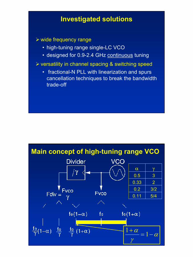
Main concept of high-tuning range VCO
20.333/20.2
γα
5/40.11
30.5
αγα
−=+ 11

4
Problems with the previous concept• For γ = 2 (1 FF), α = 0.33 … too much for a common LC VCO
• For α = 0.2 (achievable for LC VCO), γ = 3/2, but what about the duty cycle?
20.33
3/20.2
γα
5/40.11
30.5
Ideal Fvco/(3/2) with 50% duty-cycle
Fvco
Realistic Fvco/(3/2) with duty-cycle not good for mixer
More problems
• For I/Q mo-demodulation, both in-phase and in-quadrature LO signals are required
• A multiplexer is necessary for the selection of the output frequency sub-band
A more effective solution is required !!

5
High-tuning range VCO: architecture
0.83-2.5 GHz
2.5-3.75 GHz
(±20%)
High-tuning range VCO: configuration A
1/3 Fvco1/3 Fvco
2/3 Fvco
Fvco
0.83-1.25 GHz
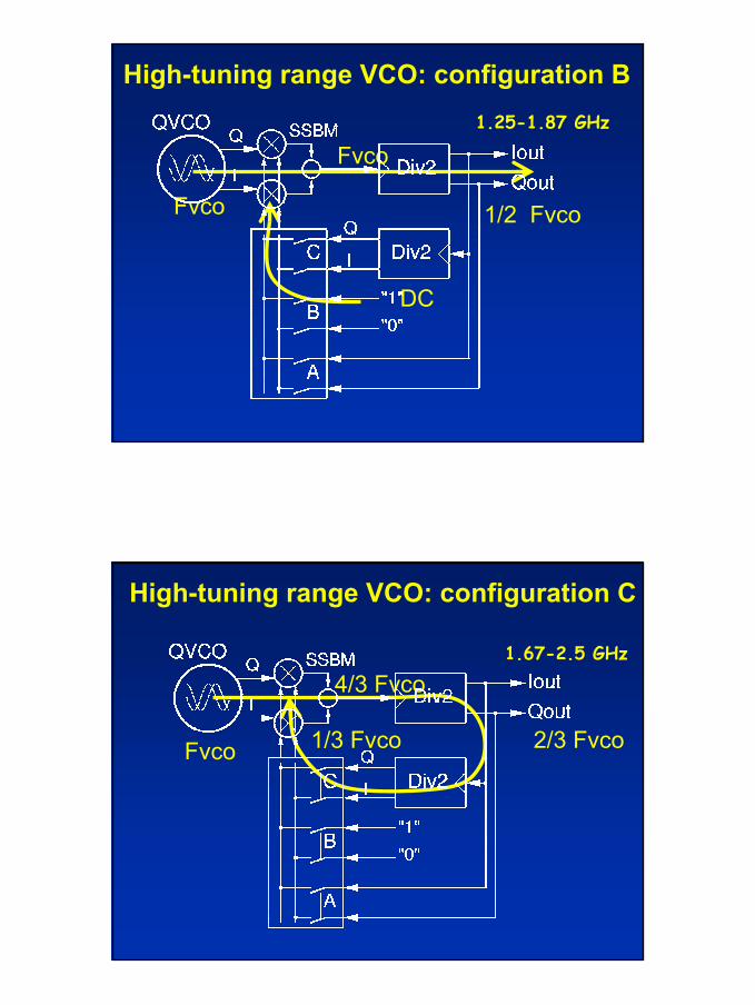
6
High-tuning range VCO: configuration B1.25-1.87 GHz
1/2 Fvco
Fvco
DC
Fvco
High-tuning range VCO: configuration C
1.67-2.5 GHz
2/3 Fvco1/3 Fvco
4/3 Fvco
Fvco

7
Schematic of the core LC-QVCO• 5-bit capacitor array for coarse tuning
• amplitude control
The quadrature is obtained by two Injection-Locked Oscillators (ILO) coupled by second harmonic
ILO
Some theoretical results on the QVCO
Quadrature oscillation is stable in the “high-swing”regime, that is also beneficial for low phase noise
“low swing” regime:
Is1 Is2 in-phaseVd1 Vd2 in-phase
“high swing” regime:
Is1 Is2 opp.-in-phaseVd1 Vd2 in-quadrature
Stability of the solutions:

8
QVCO explanation (1)
Stable solution
QVCO explanation (2)Stable solutions: depending on Is0 two possible regimes
VS and IS opposite in phase:Quadrature obtained

9
More theoretical results on the QVCOPhase-noise analysis
The QVCO and the single stage ILO have the same phase-noise x current product
nQndm
n ijQV
R rr⋅⋅⋅=
ωωθ2
1 01 nQ
ndmn i
jQVR rr
⋅⋅⋅=ωωθ22
1 01
Single stage ILO QVCO
More theoretical results on the QVCOSensitivity to tank mismatches
The quadrature error is proportional to the ratio of the bias current over the coupling current and to the quality factor Q
In the proposed scheme the output I/Q signals are generated by the DIV2 an extremely low I/Q error is NOT required from the QVCO
−⋅
+⋅=
0
02010
31
43
ωωω
sm
s
IIQerr

10
High tuning VCO: circuit design style• SCL logic for low
sensitivity to parameter variations (differential style)
• Adjustable bias current across the different sub-bands
• Differential Gilbert cells for the SSB mixer.
D-latch used in the MS-FF DIV2
Feedback path: DIV2 and MUX
DIV2
Constant output
Buffer

11
Schematic of the SSB mixer
compensation for 50% duty-cycle
Effect of the duty-cycle compensation
w/o compensation
Mixer outputs from simulations:
with compensation

12
Chip micrographSTM 0.13 µm CMOS technology
Summary of measured high-tuning range VCO performance
31.5 / 21.730.1 / 20.227.5 / 17.6 Total current (mA)< 2°< 1°< 1°Quadrature accuracy
9.585.3Reconf. curr. (mA) 22.1 / 12.2522.1 / 12.2522.1 / 12.25LC-QVCO curr. (mA)-126.5 / -120-127.5 / -122.5-130 / -126PN @ 1MHz (dBc/Hz)
1.67 / 2.51.25 /1.870.83 /1.25 Freq. range (GHz)C (2/3)B (1/2)A (1/3)Configuration

13
Phase-noise measurements
C (2 GHz)
A (1 GHz)
Meas. 0-3 GHz spectrum: configuration A

14
Meas. 0-3 GHz spectrum: configuration B
Meas. 0-3 GHz spectrum: configuration C

15
Possible origin of the subharmonicspur in configuration C
At the mixer output:
fund. @ 4/3 Fvco + tone @ Fvco (1/3 Fvco offset)
At the divider output:
fund. @ 2/3 Fvco + tone @ 1/3 Fvco (same offset)
Below -35 dBc in worst case over full frequency range
Synthesizer for reconfigurable transceivers
high-tuning range VCO
The classical integer-N architecture …
… is not adequate for channel spacing and switching speed

16
Σ∆ fractional-N synthesizer
Fractional-N obtained by varying the division ratio with a proper control sequence (α = <b(t)>):
Fout = Fref x (N+α)
b(t) = …001110101…
high-tuning range VCO
N/N+1
Why fractional synthesis?
• Easier trade off between reference frequency, loop bandwidth and output frequency resolution.– The reference frequency can be higher than
channel spacing ⇒ Increase of the loop bandwidth.
• Fine frequency step.– The frequency resolution can be much smaller
than the reference (varying α=<b(t)> in very fine steps)
• Multistandard receivers.– Reference frequency is independent on
channel spacing

17
First order Σ∆
• Assuming a constant input:– The output mean is equal to the input– The quantization noise is high-pass shaped
(see explanation on next slide)
Noise shaping in first order Σ∆
General Σ∆ modulator
Linear model with injected quantization noise
)(11
)()()(
zHzEzYzNTF +
== First order: 11)(−
=z
zH
sTF f
ffN πsin2)( = High-pass noise-shaping

18
Σ∆ of higher order and different type
• Order = number of integrators (accumulators)
• Higher order ⇒ Stronger noise shaping,
Lower Spurs
• Feedback type (single loop): critical stability.
• MASH (Multi Stage noise Shaping):
Cascade of 1st and/or 2nd order Σ∆.
Always stable.
Multibit output.
Σ∆ Noise

19
Problems in fractional synthesis
• PLL bandwidth still limited by Σ∆ quantization noise.
• High sensitivity to PFD-CP linearity (in band noise leakage).
• Actually sequences generated by Σ∆ are periodic: fractional spurs.
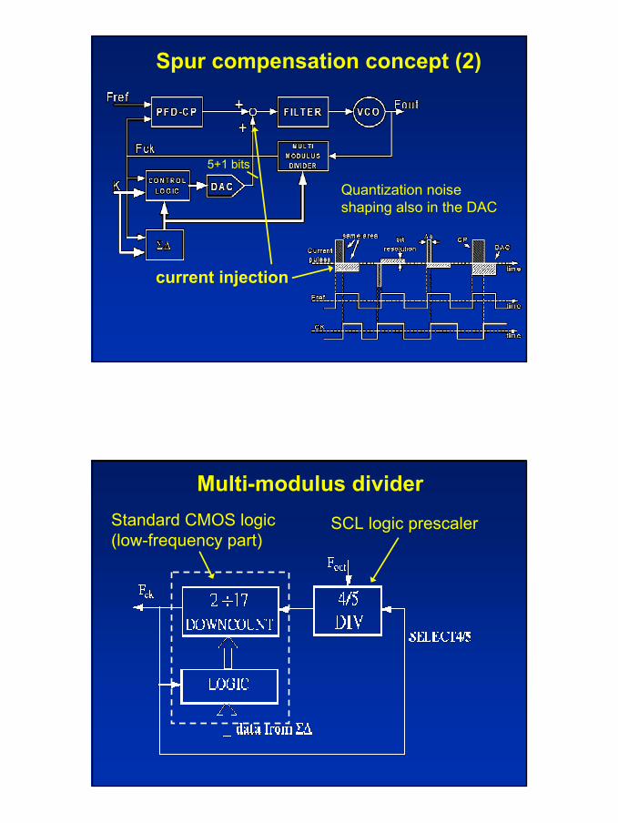
Spur compensation concept (1)
current injection related to the phase error at the input of the PFD, calculated by the control logic as
+
−+−∆=∆
KNMnxMKnn )(2)1()( πφφ
M = 2nbit
x(n) = output sequence
20
Spur compensation concept (2)
current injection
5+1 bits
Quantization noise shaping also in the DAC
Multi-modulus divider
SCL logic prescalerStandard CMOS logic (low-frequency part)

21
Linearization techniques…
dead-zonesuppression
buffers toequalize
loads
P-N mismatch
dead-zone gain enhancement
Typical linearity problems of the PFD-CP
… in the PFD
Linearization techniques … in the CP
Matching:size and bias
Vbias = low-pass filtered version of Vout

22
Alternative linearization technique: pulse injection
In lock conditions the sunk current pulse forces the PFD-CP to work in the linear part of its characteristic.
Fixed number of VCO cycles
Circuit implementation
• integrated in 0.13 µm CMOS STM technology …
• … with the exception of the Σ∆ modulator, the control logic block of the compensation scheme and the largest capacitance of the loop filter
• Σ∆ sequences are computed off-line and passed to the chip by a pattern generator
• 70 MHz differential mode clock internally divided by two (35 MHz Fref )
• total area 1.8 x 2.0 mm2

23
Measured settling time
• 75 KHz measured 3-dB closed-loop bandwidth
• 105 µs settling time
Measured phase-noise plus spursConf. C
2.4 GHz output
integer division ratio
same integer ratio + fractional w/o comp.
2 dB decrease @ 10 MHz when compensation ON (not shown)

24
The amount of spur reduction depends on loop bandwidth
700 kHz BW 200 kHz BWcurve A: integer Ncurve B: same N + fractionalcurve C: same N + fractional + spur compensation
From former STM designs
Effect of linearization techniques
15 dB reduction of the in-band fractional spur when linearization is turned ON in the PFD-CP
15 dB

25
Summary of measured performance
88Power consumption (mW)
-126 (A), -120 (B), -114.5 (C)PN @ 1 MHz offset (dBc/Hz)
-60In band fractional spur (dBc)
11 (A), 16 (B), 22 (C)Output frequency resolution (Hz)
105Linear settling time (µs)
753-dB closed loop bandwidth (KHz)
863-2403Frequency (MHz)
Conclusions
• integrated fractional synthesizer with continuous output frequency in the 0.9-2.4 GHz band
• it combines high-tuning range with high frequency resolution
• high-tuning range achieved thanks to a suitable VCO scheme
• spurs compensation + linearization techniques adopted in the synthesizer