overview or features of 8086 - rgcetpdy.ac.in year/ec t53 - mpmc/unit 4.pdf · overview or features...
TRANSCRIPT

Department of ECE Unit 4 - RGCET
ECT53 - Microprocessors and Microcontrollers 1
UNIT IV
INTEL 8086 - 16 BIT MICROPROCESSORS Evolution from 80808085 to 8086
1048766 Intel introduced 8086 microprocessor in 1978 This 16-bit microprocessor was a major
improvement over the previous generation of 80808085 series of microprocessors
1048766 In a system with pipelining the data and the address bus are busy transferring data
while the CPU is
processing information
Overview or Features of 8086
It is a 16-bit Microprocessor(μp)Itrsquos ALU internal registers works with 16bit
binary word
8086 has a 20 bit address bus can access up to 220= 1 MB memory locations
8086 has a 16bit data bus It can read or write data to a memoryport either 16bits
or 8 bit at a time
It can support up to 64K IO ports
It provides 14 16 -bit registers
Frequency range of 8086 is 6-10 MHz
It has multiplexed address and data bus AD0- AD15 and A16 ndash A19
It requires single phase clock with 33 duty cycle to provide internal timing
It can prefetch upto 6 instruction bytes from memory and queues them in order to
speed up instruction execution
It requires +5V power supply
A 40 pin dual in line package
8086 is designed to operate in two modes Minimum mode and Maximum mode
o The minimum mode is selected by applying logic 1 to the MN MX
input pin This is a single microprocessor configuration
o The maximum mode is selected by applying logic 0 to the MN MX
input pin This is a multi micro processors configuration
Department of ECE Unit 4 - RGCET
ECT53 - Microprocessors and Microcontrollers 2
31 Architechture of 8086 Functional Block diagram of 8086
8086 has two blocks Bus Interfacing Unit(BIU) and Execution Unit(EU)
The BIU performs all bus operations such as instruction fetching reading and
writing operands for memory and calculating the addresses of the memory
operands The instruction bytes are transferred to the instruction queue
EU executes instructions from the instruction system byte queue
Both units operate asynchronously to give the 8086 an overlapping instruction
fetch and execution mechanism which is called as Pipelining This results in
efficient use of the system bus and system performance
BIU contains Instruction queue Segment registers Instruction pointer Address
adder
EU contains Control circuitry Instruction decoder ALU Pointer and Index
register Flag register
Explanation of Architechture of 8086
Department of ECE Unit 4 - RGCET
ECT53 - Microprocessors and Microcontrollers 3
BUS INTERFACE UNIT
It provides a full 16 bit bidirectional data bus and 20 bit address bus
The bus interface unit is responsible for performing all external bus operations
Specifically it has the following functions
Instruction fetch Instruction queuing Operand fetch and storage Address
relocation and Bus control
The BIU uses a mechanism known as an instruction stream queue to implement a
pipeline architecture
This queue permits prefetch of up to six bytes of instruction code When ever the
queue of the BIU is not full it has room for at least two more bytes and at the
same time the EU is not requesting it to read or write operands from memory the
BIU is free to look ahead in the program by prefetching the next sequential
instruction
These prefetching instructions are held in its FIFO queue With its 16 bit data bus
the BIU fetches two instruction bytes in a single memory cycle
After a byte is loaded at the input end of the queue it automatically shifts up
through the FIFO to the empty location nearest the output
The EU accesses the queue from the output end It reads one instruction byte after
the other from the output of the queue If the queue is full and the EU is not
requesting access to operand in memory
These intervals of no bus activity which may occur between bus cycles are
known as Idle state
If the BIU is already in the process of fetching an instruction when the EU request
it to read or write operands from memory or IO the BIU first completes the
instruction fetch bus cycle before initiating the operand read write cycle
The BIU also contains a dedicated adder which is used to generate the 20bit
physical address that is output on the address bus This address is formed by
adding an appended 16 bit segment address and a 16 bit offset address
For example The physical address of the next instruction to be fetched is formed
by combining the current contents of the code segment CS register and the current
contents of the instruction pointer IP register
Department of ECE Unit 4 - RGCET
ECT53 - Microprocessors and Microcontrollers 4
The BIU is also responsible for generating bus control signals such as those for
memory read or write and IO read or write
EXECUTION UNIT
The Execution unit is responsible for decoding and executing all instructions
The EU extracts instructions from the top of the queue in the BIU decodes them
generates operands if necessary passes them to the BIU and requests it to perform
the read or write bys cycles to memory or IO and perform the operation specified
by the instruction on the operands
During the execution of the instruction the EU tests the status and control flags
and updates them based on the results of executing the instruction
If the queue is empty the EU waits for the next instruction byte to be fetched and
shifted to top of the queue
When the EU executes a branch or jump instruction it transfers control to a
location corresponding to another set of sequential instructions
Whenever this happens the BIU automatically resets the queue and then begins to
fetch instructions from this new location to refill the queue
General purpose registers
The 8086 microprocessor has a total of fourteen registers that are accessible to the
programmer It is divided into four groups They are
Four General purpose registers
Four IndexPointer registers
Four Segment registers
Two Other registers
General purpose registers
Department of ECE Unit 4 - RGCET
ECT53 - Microprocessors and Microcontrollers 5
Accumulator register consists of two 8-bit registers AL and AH which can be combined
together and used as a 16-bit register AX AL in this case contains the loworder byte of
the word and AH contains the high-order byte Accumulator can be used for IO
operations and string manipulation
Base register consists of two 8-bit registers BL and BH which can be combined together
and used as a 16-bit register BX BL in this case contains the low-order byte of the word
and BH contains the high-order byte BX register usually contains a data pointer used for
based based indexed or register indirect addressing
Count register consists of two 8-bit registers CL and CH which can be combined
together and used as a 16-bit register CX When combined CL register contains the
loworder byte of the word and CH contains the high-order byte Count register can be
used in Loop shiftrotate instructions and as a counter in string manipulation
Data register consists of two 8-bit registers DL and DH which can be combined together
and used as a 16-bit register DX When combined DL register contains the low order
byte of the word and DH contains the high-order byte Data register can be used as a port
number in IO operations In integer 32-bit multiply and divide instruction the DX
register contains high-order word of the initial or resulting number
32 Pin Diagram of 8086 and Pin description of 8086
Figure shows the Pin diagram of 8086 The description follows it
Department of ECE Unit 4 - RGCET
ECT53 - Microprocessors and Microcontrollers 6
The Microprocessor 8086 is a 16-bit CPU available in different clock rates and
packaged in a 40 pin CERDIP or plastic package
The 8086 operates in single processor or multiprocessor configuration to achieve
high performance The pins serve a particular function in minimum mode (single
processor mode ) and other function in maximum mode configuration
(multiprocessor mode )
The 8086 signals can be categorised in three groups
o The first are the signal having common functions in minimum as well as
maximum mode
o The second are the signals which have special functions for minimum
mode
o The third are the signals having special functions for maximum mode
The following signal descriptions are common for both modes
AD15-AD0 These are the time multiplexed memory IO address and data lines
o Address remains on the lines during T1 state while the data is available on
the data bus during T2 T3 Tw and T4 These lines are active high and
float to a tristate during interrupt acknowledge and local bus hold
acknowledge cycles
Department of ECE Unit 4 - RGCET
ECT53 - Microprocessors and Microcontrollers 7
A19S6A18S5A17S4A16S3 These are the time multiplexed address and
status lines
o During T1 these are the most significant address lines for memory
operations
o During IO operations these lines are low
o During memory or IO operations status information is available on those
lines for T2T3Tw and T4
o The status of the interrupt enable flag bit is updated at the beginning of
each clock cycle
o The S4 and S3 combinely indicate which segment register is presently
being used for memory accesses as in below fig
o These lines float to tri-state off during the local bus hold acknowledge
The status line S6 is always low
o The address bit are separated from the status bit using latches controlled
by the ALE signal
S4 S3 Indication
0
0
1
1
0
0
1
0
1
0
1
0
1
0
Alternate Data
Stack
Code or None
Data
Whole word
Upper byte from or to even address
Lower byte from or to even address
BHES7 The bus high enable is used to indicate the transfer of data over the
higher order ( D15-D8 ) data bus as shown in table It goes low for the data
transfer over D15-D8 and is used to derive chip selects of odd address memory
bank or peripherals BHE is low during T1 for read write and interrupt
acknowledge cycles whenever a byte is to be transferred on higher byte of data
bus The status information is available during T2 T3 and T4 The signal is active
Department of ECE Unit 4 - RGCET
ECT53 - Microprocessors and Microcontrollers 8
low and tristated during hold It is low during T1 for the first pulse of the interrupt
acknowledge cycle
RD ndash Read This signal on low indicates the peripheral that the processor is
performing memory or IO read operation RD is active low and shows the state
for T2 T3 Tw of any read cycle The signal remains tristated during the hold
acknowledge
READY This is the acknowledgement from the slow device or memory that
they have completed the data transfer The signal made available by the devices is
synchronized by the 8284A clock generator to provide ready input to the 8086
the signal is active high
INTR-Interrupt Request This is a triggered input This is sampled during the
last clock cycles of each instruction to determine the availability of the request If
any interrupt request is pending the processor enters the interrupt acknowledge
cycle This can be internally masked by resulting the interrupt enable flag This
signal is active high and internally synchronized
TEST This input is examined by a lsquoWAITrsquo instruction If the TEST pin goes
low execution will continue else the processor remains in an idle state The input
is synchronized internally during each clock cycle on leading edge of clock
CLK- Clock Input The clock input provides the basic timing for processor
operation and bus control activity Its an asymmetric square wave with 33 duty
cycle
Figure shows the Pin functions of 8086
Department of ECE Unit 4 - RGCET
ECT53 - Microprocessors and Microcontrollers 9
The following pin functions are for the minimum mode operation of 8086
MIO ndash MemoryIO This is a status line logically equivalent to S2 in maximum
mode When it is low it indicates the CPU is having an IO operation and when it
is high it indicates that the CPU is having a memory operation This line becomes
active high in the previous T4 and remains active till final T4 of the current cycle
It is tristated during local bus ldquohold acknowledge ldquo
INTA ndash Interrupt Acknowledge This signal is used as a read strobe for
interrupt acknowledge cycles ie when it goes low the processor has accepted
the interrupt
ALE ndash Address Latch Enable This output signal indicates the availability of
the valid address on the addressdata lines and is connected to latch enable input
of latches This signal is active high and is never tristated
DTR ndash Data TransmitReceive This output is used to decide the direction of
data flow through the transreceivers (bidirectional buffers) When the processor
Department of ECE Unit 4 - RGCET
ECT53 - Microprocessors and Microcontrollers 10
sends out data this signal is high and when the processor is receiving data this
signal is low
DEN ndash Data Enable This signal indicates the availability of valid data over the
addressdata lines It is used to enable the transreceivers ( bidirectional buffers ) to
separate the data from the multiplexed addressdata signal It is active from the
middle of T2 until the middle of T4 This is tristated during lsquo hold acknowledgersquo
cycle
HOLD HLDA- Acknowledge When the HOLD line goes high it indicates to
the processor that another master is requesting the bus access The processor after
receiving the HOLD request issues the hold acknowledge signal on HLDA pin in
the middle of the next clock cycle after completing the current bus cycle
At the same time the processor floats the local bus and control lines When the
processor detects the HOLD line low it lowers the HLDA signal HOLD is an
asynchronous input and is should be externally synchronized If the DMA request
is made while the CPU is performing a memory or IO cycle it will release the
local bus during T4 provided
1The request occurs on or before T2 state of the current cycle
2The current cycle is not operating over the lower byte of a word
3The current cycle is not the first acknowledge of an interrupt acknowledge sequence
4 A Lock instruction is not being executed
The following pin functions are applicable for maximum mode operation of 8086
S2 S1 S0 ndash Status Lines These are the status lines which reflect the type of
operation being carried out by the processor These become activity during T4 of
the previous cycle and active during T1 and T2 of the current bus cycles
LOCK This output pin indicates that other system bus master will be prevented
fromgaining the system bus while the LOCK signal is low The LOCK signal is
activated by the lsquoLOCKrsquo prefix instruction and remains active until the
completion of the next instruction When the CPU is executing a critical
Department of ECE Unit 4 - RGCET
ECT53 - Microprocessors and Microcontrollers 11
instruction which requires the system bus the LOCK prefix instruction ensures
that other processors connected in the system will not gain the control of the bus
The 8086 while executing the prefixed instruction asserts the bus lock signal output
which may be connected to an external bus controller By prefetching the instruction
there is a considerable speeding up in instruction execution in 8086 This is known as
instruction pipelining
S2 S1 S0 Indication
0
0
0
0
1
1
1
1
0
0
1
1
0
0
1
1
0
1
0
1
0
1
0
1
Interrupt Acknowledge
Read IO port
Write IO port
Halt
Code Access
Read Memory
Write Memory
Passive
At the starting the CSIP is loaded with the required address from which the
execution is to be started Initially the queue will be empty an the microprocessor
starts a fetch operation to bring one byte (the first byte) of instruction code if the
CSIP address is odd or two bytes at a time if the CSIP address is even
The first byte is a complete opcode in case of some instruction (one byte opcode
instruction) and is a part of opcode in case of some instructions ( two byte opcode
instructions) the remaining part of code lie in second byte
The second byte is then decoded in continuation with the first byte to decide the
instruction length and the number of subsequent bytes to be treated as instruction
data The queue is updated after every byte is read from the queue but the fetch
cycle is initiated by BIU only if at least two bytes of the queue are empty and the
EU may be concurrently executing the fetched instructions
Department of ECE Unit 4 - RGCET
ECT53 - Microprocessors and Microcontrollers 12
The next byte after the instruction is completed is again the first opcode byte of
the next instruction A similar procedure is repeated till the complete execution of
the program The fetch operation of the next instruction is overlapped with the
execution of the current instruction As in the architecture there are two separate
units namely Execution unit and Bus interface unit
While the execution unit is busy in executing an instruction after it is completely
decoded the bus interface unit may be fetching the bytes of the next instruction
from memory depending upon the queue status
QS1 QS0 Indication
0
0
1
1
0
1
0
1
No Operation
First Byte of the opcode from the queue
Empty Queue
Subsequent Byte from the Queue
RQGT0 RQGT1 ndash RequestGrant These pins are used by the other local bus
master in maximum mode to force the processor to release the local bus at the
end of the processor current bus cycle
Each of the pin is bidirectional with RQGT0 having higher priority than
RQGT1 RQGT pins have internal pull-up resistors and may be left
unconnected RequestGrant sequence is as follows
1A pulse of one clock wide from another bus master requests the bus access to 8086
2During T4(current) or T1(next) clock cycle a pulse one clock wide from 8086 to the
requesting master indicates that the 8086 has allowed the local bus to float and that it
will enter the lsquohold acknowledgersquo state at next cycle The CPU bus interface unit is likely
to be disconnected from the local bus of the system
3A one clock wide pulse from the another master indicates to the 8086 that the hold
request is about to end and the 8086 may regain control of the local bus at the next clock
cycle Thus each master to master exchange of the local bus is a sequence of 3 pulses
There must be at least one dead clock cycle after each bus exchange The request and
grant pulses are active lowFor the bus request those are received while 8086 is
Department of ECE Unit 4 - RGCET
ECT53 - Microprocessors and Microcontrollers 13
performing memory or IO cycle the granting of the bus is governed by the rules as in
case of HOLD and HLDA in minimum mode
33 Maximum Mode 8086 System
In the maximum mode the 8086 is operated by strapping the MNMX pin to
ground
In this mode the processor derives the status signal S2 S1 S0 Another chip
called bus controller derives the control signal using this status information
In the maximum mode there may be more than one microprocessor in the system
configuration
The components in the system are same as in the minimum mode system
The basic function of the bus controller chip IC8288 is to derive control signals
like RD and WR ( for memory and IO devices) DEN DTR ALE etc using the
information by the processor on the status lines
The bus controller chip has input lines S2 S1 S0 and CLK These inputs to 8288
are driven by CPU
It derives the outputs ALE DEN DTR MRDC MWTC AMWC IORC IOWC
and AIOWC The AEN IOB and CEN pins are specially useful for
multiprocessor systems
Department of ECE Unit 4 - RGCET
ECT53 - Microprocessors and Microcontrollers 14
AEN and IOB are generally grounded CEN pin is usually tied to +5V The
significance of the MCEPDEN output depends upon the status of the IOB pin
If IOB is grounded it acts as master cascade enable to control cascade 8259A
else it acts as peripheral data enable used in the multiple bus configurations
INTA pin used to issue two interrupt acknowledge pulses to the interrupt
controller or to an interrupting device
IORC IOWC are IO read command and IO write command signals respectively
These signals enable an IO interface to read or write the data from or to the
address port
The MRDC MWTC are memory read command and memory write command
signals respectively and may be used as memory read or write signals
All these command signals instructs the memory to accept or send data from or to
the bus
For both of these write command signals the advanced signals namely AIOWC
and AMWTC are available
Department of ECE Unit 4 - RGCET
ECT53 - Microprocessors and Microcontrollers 15
Here the only difference between in timing diagram between minimum mode and
maximum mode is the status signals used and the available control and advanced
command signals
R0 S1 S2 are set at the beginning of bus cycle8288 bus controller will output a
pulse as on the ALE and apply a required signal to its DT R pin during T1
In T2 8288 will set DEN=1 thus enabling transceivers and for an input it will
activate MRDC or IORC These signals are activated until T4 For an output the
AMWC or AIOWC is activated from T2 to T4 and MWTC or IOWC is activated
from T3 to T4
The status bit S0 to S2 remains active until T3 and become passive during T3 and
T4
If reader input is not activated before T3 wait state will be inserted between T3
and T4
34 Minimum Mode 8086 System
In a minimum mode 8086 system the microprocessor 8086 is operated in
minimum mode by strapping its MNMX pin to logic 1
In this mode all the control signals are given out by the microprocessor chip
itselfThere is a single microprocessor in the minimum mode system
The remaining components in the system are latches transreceivers clock
generator memory and IO devices Some type of chip selection logic may be
required for selecting memory or IO devices depending upon the address map of
the system
Latches are generally buffered output D-type flip-flops like 74LS373 or 8282
They are used for separating the valid address from the multiplexed addressdata
signals and are controlled by the ALE signal generated by 8086
Transreceivers are the bidirectional buffers and some times they are called as data
amplifiers They are required to separate the valid data from the time multiplexed
addressdata signals
They are controlled by two signals namely DEN and DTR
Department of ECE Unit 4 - RGCET
ECT53 - Microprocessors and Microcontrollers 16
The DEN signal indicates the direction of data ie from or to the processor The
system contains memory for the monitor and users program storage
Usually EPROM are used for monitor storage while RAM for users program
storage A system may contain IO devices
RQGT Timings in Maximum Mode
The requestgrant response sequence contains a series of three pulses The
requestgrant pins are checked at each rising pulse of clock input
When a request is detected and if the condition for HOLD request is satisfied the
processor issues a grant pulse over the RQGT pin immediately during T4
(current) or T1 (next) state
When the requesting master receives this pulse it accepts the control of the bus it
sends a release pulse to the processor using RQGT pin
Maximum Mode Interface
When the 8086 is set for the maximum-mode configuration it provides signals for
implementing a multiprocessor coprocessor system environment
By multiprocessor environment we mean that one microprocessor exists in the
system and that each processor is executing its own program
Usually in this type of system environment there are some system resources that
are common to all processorsThey are called as global resources There are also
Department of ECE Unit 4 - RGCET
ECT53 - Microprocessors and Microcontrollers 17
other resources that are assigned to specific processors These are known as local
or private resources
Coprocessor also means that there is a second processor in the system In this two
processor does not access the bus at the same time One passes the control of the
system bus to the other and then may suspend its operation
In the maximum-mode 8086 system facilities are provided for implementing
allocation of global resources and passing bus control to other microprocessor or
coprocessor
8288 Bus Controller ndash Bus Command and Control Signals
8086 does not directly provide all the signals that are required to control the
memory IO and interrupt interfaces
Department of ECE Unit 4 - RGCET
ECT53 - Microprocessors and Microcontrollers 18
Specially the WR MIO DTR DEN ALE and INTA signals are no longer
produced by the 8086 Instead it outputs three status signals S0 S1 S2 prior to the
initiation of each bus cycle This 3- bit bus status code identifies which type of
bus cycle is to follow
S2S1S0 are input to the external bus controller device the bus controller
generates the appropriately timed command and control signals
S2 S1 S0 Indication 8288 Command
0
0
0
0
1
1
1
1
0
0
1
1
0
0
1
1
0
1
0
1
0
1
0
1
Interrupt Acknowledge
Read IO port
Write IO port
Halt
Instruction Fetch
Read Memory
Write Memory
Passive
INTA
IORC
IOWC AIOWC
None
MRDC
MRDC
MWTC AMWC
None
The 8288 produces one or two of these eight command signals for each bus
cycles For instance when the 8086 outputs the code S2S1S0 equals 001 it
indicates that an IO read cycle is to be performed
In the code 111 is output by the 8086 it is signaling that no bus activity is to take
place
The control outputs produced by the 8288 are DEN DTR and ALE These 3
signals provide the same functions as those described for the minimum system
mode This set of bus commands and control signals is compatible with the
Multibus and industry standard for interfacing microprocessor systems
The output of 8289 are bus arbitration signals
Bus busy (BUSY) common bus request (CBRQ) bus priority out (BPRO) bus
priority in (BPRN) bus request (BREQ) and bus clock (BCLK)
Department of ECE Unit 4 - RGCET
ECT53 - Microprocessors and Microcontrollers 19
They correspond to the bus exchange signals of the Multibus and are used to lock
other processor off the system bus during the execution of an instruction by the
8086
In this way the processor can be assured of uninterrupted access to common
system resources such as global memory
Queue Status Signals Two new signals that are produced by the 8086 in the
maximum-mode system are queue status outputs QS0 and QS1 Together they
form a 2-bit ueue status code QS1QS0
Following table shows the four different queue status
QS1 QS0 Queue Status
0 (low) 0 Queue Empty The queue has been reinitialized as a
result of the execution of a transfer instruction
0 1 First Byte The byte taken from the queue was the first
byte of the instruction
1 0 Queue Empty The queue has been reinitialized as a
result of the execution of a transfer instruction
1 1 Subsequent Byte The byte taken from the queue was a
subsequent byte of the instruction
Table - Queue status codes
Local Bus Control Signal ndash Request Grant Signals In a maximum mode
configuration the minimum mode HOLD HLDA interface is also changed
These two are replaced by requestgrant lines RQ GT0 and RQ GT1
respectively They provide a prioritized bus access mechanism for accessing the
local bus
Department of ECE Unit 4 - RGCET
ECT53 - Microprocessors and Microcontrollers 20
Memory Read Timing Diagram in Maximum Mode of 8086
Memory Write Timing in Maximum mode of 8086
Department of ECE Unit 4 - RGCET
ECT53 - Microprocessors and Microcontrollers 21
Minimum Mode Interface
When the Minimum mode operation is selected the 8086 provides all control
signals needed to implement the memory and IO interface
The minimum mode signal can be divided into the following basic groups
1 Addressdata bus
2 Status
3 Control
4 Interrupt and
5 DMA
Each and every group is explained clearly
AddressData Bus
These lines serve two functions As an address bus is 20 bits long and consists of
signal lines A0 through A19 A19 represents the MSB and A0 LSB A 20bit
address gives the 8086 a 1Mbyte memory address space More over it has an
independent IO address space which is 64K bytes in length
The 16 data bus lines D0 through D15 are actually multiplexed with address lines
A0 through A15 respectively By multiplexed we mean that the bus work as an
address bus during first machine cycle and as a data bus during next machine
cycles
D15 is the MSB and D0 LSB When acting as a data bus they carry readwrite
data for memory inputoutput data for IO devices and interrupt type codes from
an interrupt controller
Department of ECE Unit 4 - RGCET
ECT53 - Microprocessors and Microcontrollers 22
Status signal
The four most significant address lines A19 through A16 are also multiplexed but
in this case with status signals S6 through S3 These status bits are output on the
bus at the same time that data are transferred over the other bus lines
Bit S4 and S3 together from a 2 bit binary code that identifies which of the 8086
internal segment registers are used to generate the physical address that was
output on the address bus during the current bus cycleCode S4S3 = 00 identifies
a register known as extra segment register as the source of the segment address
Status line S5 reflects the status of another internal characteristic of the 8086 It is
the logic level of the internal enable flag The last status bit S6 is always at the
logic 0 level
S4 S3 Segment Register
0
0
0
1
Extra
Stack
Department of ECE Unit 4 - RGCET
ECT53 - Microprocessors and Microcontrollers 23
1
1
0
1
Code none
Data
Memory segment status codes
Control Signals
The control signals are provided to support the 8086 memory IO interfaces They
control functions such as when the bus is to carry a valid address in which
direction data are to be transferred over the bus when valid write data are on the
bus and when to put read data on the system bus
ALE is a pulse to logic 1 that signals external circuitry when a valid address word
is on the bus This address must be latched in external circuitry on the 1-to-0 edge
of the pulse at ALE
Another control signal that is produced during the bus cycle is BHE bank high
enable Logic 0 on this used as a memory enable signal for the most significant
byte half of the data bus D8 through D1 These lines also serves a second
function which is as the S7 status line
Using the MIO and DTR lines the 8086 signals which type of bus cycle is in
progress and in which direction data are to be transferred over the bus The logic
level of MIO tells external circuitry whether a memory or IO transfer is taking
place over the bus Logic 1 at this output signals a memory operation and logic 0
an IO operation
The direction of data transfer over the bus is signaled by the logic level output at
DTR When this line is logic 1 during the data transfer part of a bus cycle the
bus is in the transmit mode Therefore data are either written into memory or
output to an IO device On the other hand logic 0 at DTR signals that the bus is
in the receive mode This corresponds to reading data from memory or input of
data from an input port
Department of ECE Unit 4 - RGCET
ECT53 - Microprocessors and Microcontrollers 24
The signal read RD and write WR indicates that a read bus cycle or a write bus
cycle is in progress The 8086 switches WR to logic 0 to signal external device
that valid write or output data are on the bus
On the other hand RD indicates that the 8086 is performing a read of data of the
bus During read operations one other control signal is also supplied This is DEN
( data enable) and it signals external devices when they should put data on the
bus There is one other control signal that is involved with the memory and IO
interface This is the READY signal
READY signal is used to insert wait states into the bus cycle such that it is
extended by a number of clock periods This signal is provided by an external
clock generator device and can be supplied by the memory or IO sub-system to
signal the 8086 when they are ready to permit the data transfer to be completed
Interrupt signals
The key interrupt interface signals are interrupt request (INTR) and interrupt
acknowledge ( INTA)
INTR is an input to the 8086 that can be used by an external device to signal that
it need to be serviced
Logic 1 at INTR represents an active interrupt request When an interrupt request
has been recognized by the 8086 it indicates this fact to external circuit with
pulse to logic 0 at the INTA output
The TEST input is also related to the external interrupt interface Execution of a
WAIT instruction causes the 8086 to check the logic level at the TEST input
If the logic 1 is found the MPU suspend operation and goes into the idle state
The 8086 no longer executes instructions instead it repeatedly checks the logic
level of the TEST input waiting for its transition back to logic 0
As TEST switches to 0 execution resume with the next instruction in the
program This feature can be used to synchronize the operation of the 8086 to an
event in external hardware
There are two more inputs in the interrupt interface the nonmaskable interrupt
NMI and the reset interrupt RESET
Department of ECE Unit 4 - RGCET
ECT53 - Microprocessors and Microcontrollers 25
On the 0-to-1 transition of NMI control is passed to a nonmaskable interrupt
service routine The RESET input is used to provide a hardware reset for the
8086 Switching RESET to logic 0 initializes the internal register of the 8086 and
initiates a reset service routine
DMA Interface signals
The direct memory access DMA interface of the 8086 minimum mode consist of
the HOLD and HLDA signals
When an external device wants to take control of the system bus it signals to the
8086 by switching HOLD to the logic 1 level At the completion of the current
bus cycle the 8086 enters the hold state In the hold state signal lines AD0
through AD15 A16S3 through A19S6 BHE MIO DTR RD WR DEN and
INTR are all in the high Z state
The 8086 signals external device that it is in this state by switching its HLDA
output to logic 1 level
General Bus Operation
The 8086 has a combined address and data bus commonly referred as a time
multiplexed address and data bus
The main reason behind multiplexing address and data over the same pins is the
maximum utilisation of processor pins and it facilitates the use of 40 pin standard
DIP package
The bus can be demultiplexed using a few latches and transreceivers when ever
required
Basically all the processor bus cycles consist of at least four clock cycles These
are referred to as T1 T2 T3 T4 The address is transmitted by the processor
during T1 It is present on the bus only for one cycle
The negative edge of this ALE pulse is used to separate the address and the data
or status information In maximum mode the status lines S0 S1 and S2 are used
to indicate the type of operation
Status bits S3 to S7 are multiplexed with higher order address bits and the BHE
signal Address is valid during T1 while status bits S3 to S7 are valid during T2
through T4
Department of ECE Unit 4 - RGCET
ECT53 - Microprocessors and Microcontrollers 26
Maximum mode
In the maximum mode the 8086 is operated by strapping the MNMX pin to
ground
In this mode the processor derives the status signal S2 S1 S0 Another chip
called bus controller derives the control signal using this status information
In the maximum mode there may be more than one microprocessor in the system
configuration
Minimum mode
In a minimum mode 8086 system the microprocessor 8086 is operated in
minimum mode by strapping its MNMX pin to logic 1
In this mode all the control signals are given out by the microprocessor chip
itself
There is a single microprocessor in the minimum mode system
Bus Request and Bus Grant Timings in Minimum Mode System of 8086
Department of ECE Unit 4 - RGCET
ECT53 - Microprocessors and Microcontrollers 27
Hold Response sequence The HOLD pin is checked at leading edge of each clock
pulse If it is received active by the processor before T4 of the previous cycle or
during T1 state of the current cycle the CPU activates HLDA in the next clock
cycle and for succeeding bus cycles the bus will be given to another requesting
master
The control of the bus is not regained by the processor until the requesting master
does not drop the HOLD pin low When the request is dropped by the requesting
master the HLDA is dropped by the processor at the trailing edge of the next
clock
Write Cycle Timing Diagram for Minimum Mode
The working of the minimum mode configuration system can be better described
in terms of the timing diagrams rather than qualitatively describing the operations
The opcode fetch and read cycles are similar Hence the timing diagram can be
categorized in two parts the first is the timing diagram for read cycle and the
second is the timing diagram for write cycle
Department of ECE Unit 4 - RGCET
ECT53 - Microprocessors and Microcontrollers 28
The read cycle begins in T1 with the assertion of address latch enable (ALE)
signal and also M IO signal During the negative going edge of this signal the
valid address is latched on the local bus
The BHE and A0 signals address low high or both bytes From T1 to T4 the
MIO signal indicates a memory or IO operation
At T2 the address is removed from the local bus and is sent to the output The bus
is then tristated The read (RD) control signal is also activated in T2
The read (RD) signal causes the address device to enable its data bus drivers
After RD goes low the valid data is available on the data bus
The addressed device will drive the READY line high When the processor
returns the read signal to high level the addressed device will again tristate its bus
drivers
A write cycle also begins with the assertion of ALE and the emission of the
address The MIO signal is again asserted to indicate a memory or IO operation
Department of ECE Unit 4 - RGCET
ECT53 - Microprocessors and Microcontrollers 29
In T2 after sending the address in T1 the processor sends the data to be written to
the addressed location
The data remains on the bus until middle of T4 state The WR becomes active at
the beginning of T2 (unlike RD is somewhat delayed in T2 to provide time for
floating)
The BHE and A0 signals are used to select the proper byte or bytes of memory or
IO word to be read or write
The MIO RD and WR signals indicate the type of data transfer as specified in
table below
35 Addressing Modes of 8086
Definition An instruction acts on any number of operandsThe way an instruction
accesses its operands is called its Addressing modes
Operands may be of three types
o Implicit
o Explicit
o Both Implicit and Explicit
Implicit operands mean that the instruction by definition has some specific operands
The programmers do NOT select these operands
Example Implicit operands
XLAT automatically takes AL and BX as
operands
AAM it operates on the contents of AX
Explicit operands mean the instruction operates on the operands specified by the
programmer
Example Explicit operands
MOV AX BX it takes AX and BX as
Department of ECE Unit 4 - RGCET
ECT53 - Microprocessors and Microcontrollers 30
operands
XCHG SI DI it takes SI and DI as operands
Implicit and explicit operands
Example ImplicitExplicit operands
MUL BX automatically multiply BX explicitly times
AX
The location of an operand value in memory space is called the Effective Address (EA)
We can classify the addressing modes of 8086 into four groups
Immediate addressing
Register addressing
Memory addressing
IO port addressing
The first three Addresssing modes are clearly explained
Immediate addressing mode amp Register addressing mode
Immediate Addressing Mode
In this addressing mode the operand is stored as part of the instruction The immediate
operand which is stored along with the instruction resides in the code segment -- not in
the data segment This addressing mode is also faster to execute an instruction because
the operand is read with the instruction from memory Here are some examples
Example Immediate Operands
MOV AL 20 move the constant 20 into register AL
ADD AX 5 add constant 5 to register EAX
MOV DX offset msg move the address of message to
register DX
Register addressing mode
In this addressing mode the operands may be
Department of ECE Unit 4 - RGCET
ECT53 - Microprocessors and Microcontrollers 31
reg16 16-bit general registers AX BX CX DX SI DI SP or BP
reg8 8-bit general registers AH BH CH DH AL BL CL or DL
Sreg segment registers CS DS ES or SS There is an exception CS cannot be
a destination
For register addressing modes there is no need to compute the effective address The
operand is in a register and to get the operand there is no memory access involved
Example Register Operands
MOV AX BX mov reg16 reg16
ADD AX SI add reg16 reg16
MOV DS AX mov Sreg reg16
Some rules in register addressing modes
1 You may not specify CS as the destination operand
Example mov CS 02h ndashgt wrong
2 Only one of the operands can be a segment register You cannot move data from one
segment register to another with a single mov instruction To copy the value of cs to ds
you would have to use some sequence like
mov dscs -gt wrong
mov ax cs
mov ds ax -gt the way we do it
You should never use the segment registers as data registers to hold arbitrary values
They should only contain segment addresses
Memory Addressing Modes
Memory (RAM) is the main component of a computer to store temporary data and
machine instructions In a program programmers many times need to read from and
write into memory locations
There are different forms of memory addressing modes
Department of ECE Unit 4 - RGCET
ECT53 - Microprocessors and Microcontrollers 32
1 Direct Addressing
2 Register indirect addressing
3 Based addressing
4 Indexed addressing
5 Based indexed addressing
6 Based indexed with displacement
Direct Addressing Mode amp Register Indirect Addressing Mode
Direct Addressing Mode
The instruction mov alds[8088h] loads the AL register with a copy of the byte at
memory location 8088h Likewise the instruction mov ds[1234h]dl stores the value in
the dl register to memory location 1234h By default all displacement-only values
provide offsets into the data segment If you want to provide an offset into a different
segment you must use a segment override prefix before your address For example to
access location 1234h in the extra segment (es) you would use an instruction of the form
mov axes[1234h] Likewise to access this location in the code segment you would use
the instruction mov ax cs[1234h] The ds prefix in the previous examples is not a
segment override
Department of ECE Unit 4 - RGCET
ECT53 - Microprocessors and Microcontrollers 33
The instruction mov alds[8088h] is same as mov al [8088h] If not mentioned DS
register is taken by default
Register Indirect Addressing Mode
The 80x86 CPUs let you access memory indirectly through a register using the register
indirect addressing modes There are four forms of this addressing mode on the 8086
best demonstrated by the following instructions
mov al [bx]
mov al [bp]
mov al [si]
mov al [di]
Code Example
MOV BX 100H
MOV AL [BX]
The [bx] [si] and [di] modes use the ds segment by default The [bp] addressing mode
uses the stack segment (ss) by default You can use the segment override prefix symbols
if you wish to access data in different segments The following instructions demonstrate
the use of these overrides
mov al cs[bx]
mov al ds[bp]
mov al ss[si]
mov al es[di]
Intel refers to [bx] and [bp] as base addressing modes and bx and bp as base registers (in
fact bp stands for base pointer) Intel refers to the [si] and [di] addressing modes as
indexed addressing modes (si stands for source index di stands for destination index)
However these addressing modes are functionally equivalent This text will call these
forms register indirect modes to be consistent
Department of ECE Unit 4 - RGCET
ECT53 - Microprocessors and Microcontrollers 34
Based Addressing Mode and Indexed Addressing Modes
Based Addressing Mode
8-bit or 16-bit instruction operand is added to the contents of a base register (BX or BP)
the resulting value is a pointer to location where data resides
Mov al [bx][si]
Mov bl [bp][di]
Mov cl [bp][di]
Code Example
If bx=1000h
si=0880h
Mov AL [1000+880]
Mov AL[1880]
Indexed Addressing Modes
The indexed addressing modes use the following syntax
mov al [bx+disp]
mov al [bp+disp]
mov al [si+disp]
mov al [di+disp]
Code Example
MOV BX 100H
MOV AL [BX + 15]
MOV AL [BX + 16]
If bx contains 1000h then the instruction mov cl [bx+20h] will load cl from memory
location ds1020h Likewise if bp contains 2020h mov dh [bp+1000h] will load dh from
location ss3020 The offsets generated by these addressing modes are the sum of the
constant and the specified register The addressing modes involving bx si and di all use
Department of ECE Unit 4 - RGCET
ECT53 - Microprocessors and Microcontrollers 35
the data segment the [bp+disp] addressing mode uses the stack segment by default As
with the register indirect addressing modes you can use the segment override prefixes to
specify a different segment
mov al ss[bx+disp]
mov al es[bp+disp]
mov al cs[si+disp]
mov al ss[di+disp]
Based Indexed Addressing Modes amp Based Indexed Plus Displacement Addressing Mode
Based Indexed Addressing Modes
The based indexed addressing modes are simply combinations of the register indirect
addressing modes These addressing modes form the offset by adding together a base
register (bx or bp) and an index register (si or di) The allowable forms for these
addressing modes are
mov al [bx+si]
mov al [bx+di]
mov al [bp+si]
mov al [bp+di]
Code Example
MOV BX 100H
MOV SI 200H
MOV AL [BX + SI]
INC BX
INC SI
Department of ECE Unit 4 - RGCET
ECT53 - Microprocessors and Microcontrollers 36
Suppose that bx contains 1000h and si contains 880h Then the instruction mov al[bx][si]
would load al from location DS1880h Likewise if bp contains 1598h and di contains
1004 mov ax[bp+di] will load the 16 bits in ax from locations SS259C and SS259D
The addressing modes that do not involve bp use the data segment by default Those that
have bp as an operand use the stack segment by default
Based Indexed Plus Displacement Addressing Mode
These addressing modes are a slight modification of the baseindexed addressing modes
with the addition of an eight bit or sixteen bit constant The following are some examples
of these addressing modes
mov al disp[bx][si]
mov al disp[bx+di]
mov al [bp+si+disp]
mov al [bp][di][disp]
Department of ECE Unit 4 - RGCET
ECT53 - Microprocessors and Microcontrollers 37
Code Example
MOV BX 100H
MOV SI 200H
MOV AL [BX + SI +100H]
INC BX
INC SI
Index or Pointer Registers
These registers can also be called as Special Purpose registers
Department of ECE Unit 4 - RGCET
ECT53 - Microprocessors and Microcontrollers 38
Stack Pointer (SP) is a 16-bit register pointing to program stack ie it is used to hold the
address of the top of stack The stack is maintained as a LIFO with its bottom at the start
of the stack segment (specified by the SS segment register)Unlike the SP register the BP
can be used to specify the offset of other program segments
Base Pointer (BP) is a 16-bit register pointing to data in stack segment It is usually used
by subroutines to locate variables that were passed on the stack by a calling program BP
register is usually used for based based indexed or register indirect addressing
Source Index (SI) is a 16-bit register SI is used for indexed based indexed and register
indirect addressing as well as a source data address in string manipulation instructions
Used in conjunction with the DS register to point to data locations in the data segment
Destination Index (DI) is a 16-bit register Used in conjunction with the ES register in
string operations DI is used for indexed based indexed and register indirect addressing
as well as a destination data address in string manipulation instructions In short
Destination Index and SI Source Index registers are used to hold address
Segment Registers
Most of the registers contain datainstruction offsets within 64 KB memory segment
There are four different 64 KB segments for instructions stack data and extra data To
specify where in 1 MB of processor memory these 4 segments are located the processor
uses four segment registers
Department of ECE Unit 4 - RGCET
ECT53 - Microprocessors and Microcontrollers 39
Code segment (CS) is a 16-bit register containing address of 64 KB segment with
processor instructions The processor uses CS segment for all accesses to instructions
referenced by instruction pointer (IP) register CS register cannot be changed directly
The CS register is automatically updated during far jump far call and far return
instructions
Stack segment (SS) is a 16-bit register containing address of 64KB segment with
program stack By default the processor assumes that all data referenced by the stack
pointer (SP) and base pointer (BP) registers is located in the stack segment SS register
can be changed directly using POP instruction
Data segment (DS) is a 16-bit register containing address of 64KB segment with
program data By default the processor assumes that all data referenced by general
registers (AX BX CX DX) and index register (SI DI) is located in the data segment
DS register can be changed directly using POP and LDS instructions
Extra segment (ES) used to hold the starting address of Extra segment Extra segment is
provided for programs that need to access a second data segment Segment registers
cannot be used in arithmetic operations
Other registers of 8086
Instruction Pointer (IP) is a 16-bit register This is a crucially important register which
is used to control which instruction the CPU executes The ip or program counter is used
to store the memory location of the next instruction to be executed The CPU checks the
program counter to ascertain which instruction to carry out next It then updates the
program counter to point to the next instruction Thus the program counter will always
point to the next instruction to be executed
Flag Register contains a group of status bits called flags that indicate the status of the
CPU or the result of arithmetic operations There are two types of flags
Department of ECE Unit 4 - RGCET
ECT53 - Microprocessors and Microcontrollers 40
1 The status flags which reflect the result of executing an instruction The programmer
cannot setreset these flags directly
2 The control flags enable or disable certain CPU operations The programmer can
setreset these bits to control the CPUs operation
Nine individual bits of the status register are used as control flags (3 of them) and status
flags (6 of them)The remaining 7 are not used
A flag can only take on the values 0 and 1 We say a flag is set if it has the value 1The
status flags are used to record specific characteristics of arithmetic and of logical
instructions
Control Flags There are three control flags
1 The Direction Flag (D) Affects the direction of moving data blocks by such
instructions as MOVS CMPS and SCAS The flag values are 0 = up and 1 = down and
can be setreset by the STD (set D) and CLD (clear D) instructions
2 The Interrupt Flag (I) Dictates whether or not system interrupts can occur Interrupts
are actions initiated by hardware block such as input devices that will interrupt the
normal execution of programs The flag values are 0 = disable interrupts or 1 = enable
interrupts and can be manipulated by the CLI (clear I) and STI (set I) instructions
Department of ECE Unit 4 - RGCET
ECT53 - Microprocessors and Microcontrollers 41
3 The Trap Flag (T) Determines whether or not the CPU is halted after the execution
of each instruction When this flag is set (ie = 1) the programmer can single step
through his program to debug any errors When this flag = 0 this feature is off This flag
can be set by the INT 3 instruction
Status Flags There are six status flags
1 The Carry Flag (C) This flag is set when the result of an unsigned arithmetic
operation is too large to fit in the destination register This happens when there is an end
carry in an addition operation or there an end borrows in a subtraction operation A value
of 1 = carry and 0 = no carry
2 The Overflow Flag (O) This flag is set when the result of a signed arithmetic
operation is too large to fit in the destination register (ie when an overflow occurs)
Overflow can occur when adding two numbers with the same sign (ie both positive or
both negative) A value of 1 = overflow and 0 = no overflow
3 The Sign Flag (S) This flag is set when the result of an arithmetic or logic operation
is negative This flag is a copy of the MSB of the result (ie the sign bit) A value of 1
means negative and 0 = positive
4 The Zero Flag (Z) This flag is set when the result of an arithmetic or logic operation
is equal to zero A value of 1 means the result is zero and a value of 0 means the result is
not zero
5 The Auxiliary Carry Flag (A) This flag is set when an operation causes a carry from
bit 3 to bit 4 (or a borrow from bit 4 to bit 3) of an operand A value of 1 = carry and 0 =
no carry
6 The Parity Flag (P) This flags reflects the number of 1s in the result of an operation
If the number of 1s is even its value = 1 and if the number of 1s is odd then its value = 0
36 8086 Instruction Set and its Classification
The instructions of 8086 are classified into SIX groups They are
1 DATA TRANSFER INSTRUCTIONS
Department of ECE Unit 4 - RGCET
ECT53 - Microprocessors and Microcontrollers 42
2 ARITHMETIC INSTRUCTIONS
3 BIT MANIPULATION INSTRUCTIONS
4 STRING INSTRUCTIONS
5 PROGRAM EXECUTION TRANSFER INSTRUCTIONS
6 PROCESS CONTROL INSTRUCTIONS
1DATA TRANSFER INSTRUCTIONS
The DATA TRANSFER INSTRUCTIONS are those which transfers the DATA from
any one source to any one destinationThe datas may be of any type They are again
classified into four groupsThey are
GENERAL ndash PURPOSE
BYTE OR WORD
TRANSFER INSTRUCTIONS
SIMPLE INPUT AND
OUTPUT PORT
TRANSFER
INSTRUCTION
SPECIAL ADDRESS
TRANSFER
INSTRUCTION
FLAG
TRANSFER
INSTRUCTIONS
MOV
PUSH
POP
XCHG
XLAT
IN
OUT
LEA
LDS
LES
LAHF
SAHF
PUSHF
POPF
2ARITHMETIC INSTRUCTIONS
These instructions are those which are useful to perform Arithmetic calculations such as
addition subtraction multiplication and divisionThey are again classified into four
groupsThey are
ADDITION
INSTRUCTIONS
SUBTRACTION
INSTRUCTIONS
MULTIPLICATION
INSTRUCTIONS
DIVISION
INSTRUCTIONS
ADD
ADC
INC
AAA
DAA
SUB
SBB
DEC
NEG
CMP
AAS
DAS
MUL
IMUL
AAM
DIV
IDIV
AAD
CBW
CWD
3BIT MANIPULATION INSTRUCTIONS
Department of ECE Unit 4 - RGCET
ECT53 - Microprocessors and Microcontrollers 43
These instructions are used to perform Bit wise operations
LOGICAL INSTRUCTIONS SHIFT INSTRUCTIONS ROTATE INSTRUCTIONS
NOT
AND
OR
XOR
TEST
SHL SAL
SHR
SAR
ROL
ROR
RCL
RCR
4 STRING INSTRUCTIONS
The string instructions function easily on blocks of memoryThey are user friendly
instructions which help for easy program writing and execution They can speed up the
manipulating codeThey are useful in array handling tables and records
STRING INSTRUCTIONS
REP
REPE REPZ
REPNE REPNZ
MOVS MOVSB MOVSW
COMPS COMPSB
COMPSW
SCAS SCASB SCASW
LODS LODSB LODSW
STOS STOSB STOSW
5PROGRAM EXECUTION TRANSFER INSTRUCTIONS
These instructions transfer the program control from one address to other address ( Not
in a sequence) They are again classified into four groupsThey are
UNCONDITIONAL
TRANSFER
INSTRUCTIONS
CONDITIONAL
TRANSFER
INSTRUCTIONS
ITERATION CONTROL
INSTRUCTIONS
INTERRUPT
INSTRUCTIONS
CALL
RET
JMP
JA JNBE
JAE JNB
JB JNAE
JBE JNA
JC
JE JZ
JLE JNG
JNC
JNE JNZ
JNO
JNP JPO
JNS
LOOP
LOOPE LOOPZ
LOOPNE LOOPNZ
JCXZ
INT
INTO
IRET
Department of ECE Unit 4 - RGCET
ECT53 - Microprocessors and Microcontrollers 44
JG JNLE
JGE JNL
JL JNGE
JO
JP JPE
JS
6PROCESS CONTROL INSTRUCTIONS
These instructions are used to change the process of the Microprocessor They change the
process with the stored information They are again classified into Two groupsThey are
FLAG SET CLEAR
INSTRUCTIONS
EXTERNAL HARDWARE
SYNCHRONIZATION
INSTRUCTIONS
STC
CLC
CMC
STD
CLD
STI
CLI
HLT
WAIT
ESC
LOCK
NOP
37 Interrupts
Definition The meaning of lsquointerruptsrsquo is to break the sequence of operationWhile the
cpu is executing a programon lsquointerruptrsquo breaks the normal sequence of execution of
instructions diverts its execution to some other program called Interrupt Service Routine
(ISR)After executing ISR the control is transferred back again to the main
programInterrupt processing is an alternative to polling
Need for Interrupt Interrupts are particularly useful when interfacing IO devices that
provide or require data at relatively low data transfer rate
Types of Interrupts There are two types of Interrupts in 8086 They are
(i)Hardware Interrupts and
(ii)Software Interrupts
Department of ECE Unit 4 - RGCET
ECT53 - Microprocessors and Microcontrollers 45
(i) Hardware Interrupts (External Interrupts) The Intel microprocessors support
hardware interrupts through
Two pins that allow interrupt requests INTR and NMI
One pin that acknowledges INTA the interrupt requested on INTR
INTR and NMI
INTR is a maskable hardware interrupt The interrupt can be enableddisabled
using STICLI instructions or using more complicated method of updating the
FLAGS register with the help of the POPF instruction
When an interrupt occurs the processor stores FLAGS register into stack
disables further interrupts fetches from the bus one byte representing interrupt
type and jumps to interrupt processing routine address of which is stored in
location 4 ltinterrupt typegt Interrupt processing routine should return with the
IRET instruction
NMI is a non-maskable interrupt Interrupt is processed in the same way as the
INTR interrupt Interrupt type of the NMI is 2 ie the address of the NMI
processing routine is stored in location 0008h This interrupt has higher priority
than the maskable interrupt
ndash Ex NMI INTR
(ii) Software Interrupts (Internal Interrupts and Instructions) Software interrupts can
be caused by
INT instruction - breakpoint interrupt This is a type 3 interrupt
INT ltinterrupt numbergt instruction - any one interrupt from available 256
interrupts
INTO instruction - interrupt on overflow
Single-step interrupt - generated if the TF flag is set This is a type 1 interrupt
When the CPU processes this interrupt it clears TF flag before calling the
interrupt processing routine
Processor exceptions Divide Error (Type 0) Unused Opcode (type 6) and Escape
opcode (type 7)
Software interrupt processing is the same as for the hardware interrupts
Department of ECE Unit 4 - RGCET
ECT53 - Microprocessors and Microcontrollers 46
- Ex INT n (Software Instructions)
Control is provided through
o IF and TF flag bits
o IRET and IRETD
Performance of Hardware Interrupts
NMI Non maskable interrupts - TYPE 2 Interrupt
INTR Interrupt request - Between 20H and FFH
Interrupt Priority Structure
Performance of Software Interrupts
1 It decrements SP by 2 and pushes the flag register on the stack
2 Disables INTR by clearing the IF
3 It resets the TF in the flag Register
5 It decrements SP by 2 and pushes CS on the stack
Department of ECE Unit 4 - RGCET
ECT53 - Microprocessors and Microcontrollers 47
6 It decrements SP by 2 and pushes IP on the stack
6 Fetch the ISR address from the interrupt vector table
38 Other microprocessors the 80286 80386 and 80486 1048766 80286 Intel introduced 80286 in 1982
bull With 16-bit internal and external data bus
bull 24-bit address bus (224 = 16 megabyte)
bull virtual memory a way of fooling the microprocessor into thinking that it has access to
unlimited
memory by swapping data between disk storage and RAM
bull Real mode (faster operation with maximum of 1 Mbytes of memory) vs Protected
mode
protecting the operating system for accidental or deliberate destruction of the user
Protected
mode is slower but can use 16 Mbytes of memory
1048766 80386 introduced in 1985 also known as (80386DX)
bull With 32-bit internal and external data bus
bull 32-bit address bus (232 = 4 gigabyte-physical memory) With virtual memory 64
terabytes(246)
bull 80386SX was later introduced with the same internal structure with 16-bit external data
bus and
24-bit address bus 80386SX was much cheaper
1048766 All microprocessors discussed so far were general-purpose microprocessors and could
not handle
mathematical operations rapidly For this reason 8087 80287 80387 numeric data
processing chips
called math co-processors were used
1048766 80486 introduced in 1989 with 32-bit internal-external data bus and 32-bit address
bus
bull built in math co-processor in a single chip
bull Introduction of cache memory ( Static RAM with very fast access time)
Evolution of Intels Microprocessors

Department of ECE Unit 4 - RGCET
ECT53 - Microprocessors and Microcontrollers 5
Accumulator register consists of two 8-bit registers AL and AH which can be combined
together and used as a 16-bit register AX AL in this case contains the loworder byte of
the word and AH contains the high-order byte Accumulator can be used for IO
operations and string manipulation
Base register consists of two 8-bit registers BL and BH which can be combined together
and used as a 16-bit register BX BL in this case contains the low-order byte of the word
and BH contains the high-order byte BX register usually contains a data pointer used for
based based indexed or register indirect addressing
Count register consists of two 8-bit registers CL and CH which can be combined
together and used as a 16-bit register CX When combined CL register contains the
loworder byte of the word and CH contains the high-order byte Count register can be
used in Loop shiftrotate instructions and as a counter in string manipulation
Data register consists of two 8-bit registers DL and DH which can be combined together
and used as a 16-bit register DX When combined DL register contains the low order
byte of the word and DH contains the high-order byte Data register can be used as a port
number in IO operations In integer 32-bit multiply and divide instruction the DX
register contains high-order word of the initial or resulting number
32 Pin Diagram of 8086 and Pin description of 8086
Figure shows the Pin diagram of 8086 The description follows it
Department of ECE Unit 4 - RGCET
ECT53 - Microprocessors and Microcontrollers 6
The Microprocessor 8086 is a 16-bit CPU available in different clock rates and
packaged in a 40 pin CERDIP or plastic package
The 8086 operates in single processor or multiprocessor configuration to achieve
high performance The pins serve a particular function in minimum mode (single
processor mode ) and other function in maximum mode configuration
(multiprocessor mode )
The 8086 signals can be categorised in three groups
o The first are the signal having common functions in minimum as well as
maximum mode
o The second are the signals which have special functions for minimum
mode
o The third are the signals having special functions for maximum mode
The following signal descriptions are common for both modes
AD15-AD0 These are the time multiplexed memory IO address and data lines
o Address remains on the lines during T1 state while the data is available on
the data bus during T2 T3 Tw and T4 These lines are active high and
float to a tristate during interrupt acknowledge and local bus hold
acknowledge cycles
Department of ECE Unit 4 - RGCET
ECT53 - Microprocessors and Microcontrollers 7
A19S6A18S5A17S4A16S3 These are the time multiplexed address and
status lines
o During T1 these are the most significant address lines for memory
operations
o During IO operations these lines are low
o During memory or IO operations status information is available on those
lines for T2T3Tw and T4
o The status of the interrupt enable flag bit is updated at the beginning of
each clock cycle
o The S4 and S3 combinely indicate which segment register is presently
being used for memory accesses as in below fig
o These lines float to tri-state off during the local bus hold acknowledge
The status line S6 is always low
o The address bit are separated from the status bit using latches controlled
by the ALE signal
S4 S3 Indication
0
0
1
1
0
0
1
0
1
0
1
0
1
0
Alternate Data
Stack
Code or None
Data
Whole word
Upper byte from or to even address
Lower byte from or to even address
BHES7 The bus high enable is used to indicate the transfer of data over the
higher order ( D15-D8 ) data bus as shown in table It goes low for the data
transfer over D15-D8 and is used to derive chip selects of odd address memory
bank or peripherals BHE is low during T1 for read write and interrupt
acknowledge cycles whenever a byte is to be transferred on higher byte of data
bus The status information is available during T2 T3 and T4 The signal is active
Department of ECE Unit 4 - RGCET
ECT53 - Microprocessors and Microcontrollers 8
low and tristated during hold It is low during T1 for the first pulse of the interrupt
acknowledge cycle
RD ndash Read This signal on low indicates the peripheral that the processor is
performing memory or IO read operation RD is active low and shows the state
for T2 T3 Tw of any read cycle The signal remains tristated during the hold
acknowledge
READY This is the acknowledgement from the slow device or memory that
they have completed the data transfer The signal made available by the devices is
synchronized by the 8284A clock generator to provide ready input to the 8086
the signal is active high
INTR-Interrupt Request This is a triggered input This is sampled during the
last clock cycles of each instruction to determine the availability of the request If
any interrupt request is pending the processor enters the interrupt acknowledge
cycle This can be internally masked by resulting the interrupt enable flag This
signal is active high and internally synchronized
TEST This input is examined by a lsquoWAITrsquo instruction If the TEST pin goes
low execution will continue else the processor remains in an idle state The input
is synchronized internally during each clock cycle on leading edge of clock
CLK- Clock Input The clock input provides the basic timing for processor
operation and bus control activity Its an asymmetric square wave with 33 duty
cycle
Figure shows the Pin functions of 8086
Department of ECE Unit 4 - RGCET
ECT53 - Microprocessors and Microcontrollers 9
The following pin functions are for the minimum mode operation of 8086
MIO ndash MemoryIO This is a status line logically equivalent to S2 in maximum
mode When it is low it indicates the CPU is having an IO operation and when it
is high it indicates that the CPU is having a memory operation This line becomes
active high in the previous T4 and remains active till final T4 of the current cycle
It is tristated during local bus ldquohold acknowledge ldquo
INTA ndash Interrupt Acknowledge This signal is used as a read strobe for
interrupt acknowledge cycles ie when it goes low the processor has accepted
the interrupt
ALE ndash Address Latch Enable This output signal indicates the availability of
the valid address on the addressdata lines and is connected to latch enable input
of latches This signal is active high and is never tristated
DTR ndash Data TransmitReceive This output is used to decide the direction of
data flow through the transreceivers (bidirectional buffers) When the processor
Department of ECE Unit 4 - RGCET
ECT53 - Microprocessors and Microcontrollers 10
sends out data this signal is high and when the processor is receiving data this
signal is low
DEN ndash Data Enable This signal indicates the availability of valid data over the
addressdata lines It is used to enable the transreceivers ( bidirectional buffers ) to
separate the data from the multiplexed addressdata signal It is active from the
middle of T2 until the middle of T4 This is tristated during lsquo hold acknowledgersquo
cycle
HOLD HLDA- Acknowledge When the HOLD line goes high it indicates to
the processor that another master is requesting the bus access The processor after
receiving the HOLD request issues the hold acknowledge signal on HLDA pin in
the middle of the next clock cycle after completing the current bus cycle
At the same time the processor floats the local bus and control lines When the
processor detects the HOLD line low it lowers the HLDA signal HOLD is an
asynchronous input and is should be externally synchronized If the DMA request
is made while the CPU is performing a memory or IO cycle it will release the
local bus during T4 provided
1The request occurs on or before T2 state of the current cycle
2The current cycle is not operating over the lower byte of a word
3The current cycle is not the first acknowledge of an interrupt acknowledge sequence
4 A Lock instruction is not being executed
The following pin functions are applicable for maximum mode operation of 8086
S2 S1 S0 ndash Status Lines These are the status lines which reflect the type of
operation being carried out by the processor These become activity during T4 of
the previous cycle and active during T1 and T2 of the current bus cycles
LOCK This output pin indicates that other system bus master will be prevented
fromgaining the system bus while the LOCK signal is low The LOCK signal is
activated by the lsquoLOCKrsquo prefix instruction and remains active until the
completion of the next instruction When the CPU is executing a critical
Department of ECE Unit 4 - RGCET
ECT53 - Microprocessors and Microcontrollers 11
instruction which requires the system bus the LOCK prefix instruction ensures
that other processors connected in the system will not gain the control of the bus
The 8086 while executing the prefixed instruction asserts the bus lock signal output
which may be connected to an external bus controller By prefetching the instruction
there is a considerable speeding up in instruction execution in 8086 This is known as
instruction pipelining
S2 S1 S0 Indication
0
0
0
0
1
1
1
1
0
0
1
1
0
0
1
1
0
1
0
1
0
1
0
1
Interrupt Acknowledge
Read IO port
Write IO port
Halt
Code Access
Read Memory
Write Memory
Passive
At the starting the CSIP is loaded with the required address from which the
execution is to be started Initially the queue will be empty an the microprocessor
starts a fetch operation to bring one byte (the first byte) of instruction code if the
CSIP address is odd or two bytes at a time if the CSIP address is even
The first byte is a complete opcode in case of some instruction (one byte opcode
instruction) and is a part of opcode in case of some instructions ( two byte opcode
instructions) the remaining part of code lie in second byte
The second byte is then decoded in continuation with the first byte to decide the
instruction length and the number of subsequent bytes to be treated as instruction
data The queue is updated after every byte is read from the queue but the fetch
cycle is initiated by BIU only if at least two bytes of the queue are empty and the
EU may be concurrently executing the fetched instructions
Department of ECE Unit 4 - RGCET
ECT53 - Microprocessors and Microcontrollers 12
The next byte after the instruction is completed is again the first opcode byte of
the next instruction A similar procedure is repeated till the complete execution of
the program The fetch operation of the next instruction is overlapped with the
execution of the current instruction As in the architecture there are two separate
units namely Execution unit and Bus interface unit
While the execution unit is busy in executing an instruction after it is completely
decoded the bus interface unit may be fetching the bytes of the next instruction
from memory depending upon the queue status
QS1 QS0 Indication
0
0
1
1
0
1
0
1
No Operation
First Byte of the opcode from the queue
Empty Queue
Subsequent Byte from the Queue
RQGT0 RQGT1 ndash RequestGrant These pins are used by the other local bus
master in maximum mode to force the processor to release the local bus at the
end of the processor current bus cycle
Each of the pin is bidirectional with RQGT0 having higher priority than
RQGT1 RQGT pins have internal pull-up resistors and may be left
unconnected RequestGrant sequence is as follows
1A pulse of one clock wide from another bus master requests the bus access to 8086
2During T4(current) or T1(next) clock cycle a pulse one clock wide from 8086 to the
requesting master indicates that the 8086 has allowed the local bus to float and that it
will enter the lsquohold acknowledgersquo state at next cycle The CPU bus interface unit is likely
to be disconnected from the local bus of the system
3A one clock wide pulse from the another master indicates to the 8086 that the hold
request is about to end and the 8086 may regain control of the local bus at the next clock
cycle Thus each master to master exchange of the local bus is a sequence of 3 pulses
There must be at least one dead clock cycle after each bus exchange The request and
grant pulses are active lowFor the bus request those are received while 8086 is
Department of ECE Unit 4 - RGCET
ECT53 - Microprocessors and Microcontrollers 13
performing memory or IO cycle the granting of the bus is governed by the rules as in
case of HOLD and HLDA in minimum mode
33 Maximum Mode 8086 System
In the maximum mode the 8086 is operated by strapping the MNMX pin to
ground
In this mode the processor derives the status signal S2 S1 S0 Another chip
called bus controller derives the control signal using this status information
In the maximum mode there may be more than one microprocessor in the system
configuration
The components in the system are same as in the minimum mode system
The basic function of the bus controller chip IC8288 is to derive control signals
like RD and WR ( for memory and IO devices) DEN DTR ALE etc using the
information by the processor on the status lines
The bus controller chip has input lines S2 S1 S0 and CLK These inputs to 8288
are driven by CPU
It derives the outputs ALE DEN DTR MRDC MWTC AMWC IORC IOWC
and AIOWC The AEN IOB and CEN pins are specially useful for
multiprocessor systems
Department of ECE Unit 4 - RGCET
ECT53 - Microprocessors and Microcontrollers 14
AEN and IOB are generally grounded CEN pin is usually tied to +5V The
significance of the MCEPDEN output depends upon the status of the IOB pin
If IOB is grounded it acts as master cascade enable to control cascade 8259A
else it acts as peripheral data enable used in the multiple bus configurations
INTA pin used to issue two interrupt acknowledge pulses to the interrupt
controller or to an interrupting device
IORC IOWC are IO read command and IO write command signals respectively
These signals enable an IO interface to read or write the data from or to the
address port
The MRDC MWTC are memory read command and memory write command
signals respectively and may be used as memory read or write signals
All these command signals instructs the memory to accept or send data from or to
the bus
For both of these write command signals the advanced signals namely AIOWC
and AMWTC are available
Department of ECE Unit 4 - RGCET
ECT53 - Microprocessors and Microcontrollers 15
Here the only difference between in timing diagram between minimum mode and
maximum mode is the status signals used and the available control and advanced
command signals
R0 S1 S2 are set at the beginning of bus cycle8288 bus controller will output a
pulse as on the ALE and apply a required signal to its DT R pin during T1
In T2 8288 will set DEN=1 thus enabling transceivers and for an input it will
activate MRDC or IORC These signals are activated until T4 For an output the
AMWC or AIOWC is activated from T2 to T4 and MWTC or IOWC is activated
from T3 to T4
The status bit S0 to S2 remains active until T3 and become passive during T3 and
T4
If reader input is not activated before T3 wait state will be inserted between T3
and T4
34 Minimum Mode 8086 System
In a minimum mode 8086 system the microprocessor 8086 is operated in
minimum mode by strapping its MNMX pin to logic 1
In this mode all the control signals are given out by the microprocessor chip
itselfThere is a single microprocessor in the minimum mode system
The remaining components in the system are latches transreceivers clock
generator memory and IO devices Some type of chip selection logic may be
required for selecting memory or IO devices depending upon the address map of
the system
Latches are generally buffered output D-type flip-flops like 74LS373 or 8282
They are used for separating the valid address from the multiplexed addressdata
signals and are controlled by the ALE signal generated by 8086
Transreceivers are the bidirectional buffers and some times they are called as data
amplifiers They are required to separate the valid data from the time multiplexed
addressdata signals
They are controlled by two signals namely DEN and DTR
Department of ECE Unit 4 - RGCET
ECT53 - Microprocessors and Microcontrollers 16
The DEN signal indicates the direction of data ie from or to the processor The
system contains memory for the monitor and users program storage
Usually EPROM are used for monitor storage while RAM for users program
storage A system may contain IO devices
RQGT Timings in Maximum Mode
The requestgrant response sequence contains a series of three pulses The
requestgrant pins are checked at each rising pulse of clock input
When a request is detected and if the condition for HOLD request is satisfied the
processor issues a grant pulse over the RQGT pin immediately during T4
(current) or T1 (next) state
When the requesting master receives this pulse it accepts the control of the bus it
sends a release pulse to the processor using RQGT pin
Maximum Mode Interface
When the 8086 is set for the maximum-mode configuration it provides signals for
implementing a multiprocessor coprocessor system environment
By multiprocessor environment we mean that one microprocessor exists in the
system and that each processor is executing its own program
Usually in this type of system environment there are some system resources that
are common to all processorsThey are called as global resources There are also
Department of ECE Unit 4 - RGCET
ECT53 - Microprocessors and Microcontrollers 17
other resources that are assigned to specific processors These are known as local
or private resources
Coprocessor also means that there is a second processor in the system In this two
processor does not access the bus at the same time One passes the control of the
system bus to the other and then may suspend its operation
In the maximum-mode 8086 system facilities are provided for implementing
allocation of global resources and passing bus control to other microprocessor or
coprocessor
8288 Bus Controller ndash Bus Command and Control Signals
8086 does not directly provide all the signals that are required to control the
memory IO and interrupt interfaces
Department of ECE Unit 4 - RGCET
ECT53 - Microprocessors and Microcontrollers 18
Specially the WR MIO DTR DEN ALE and INTA signals are no longer
produced by the 8086 Instead it outputs three status signals S0 S1 S2 prior to the
initiation of each bus cycle This 3- bit bus status code identifies which type of
bus cycle is to follow
S2S1S0 are input to the external bus controller device the bus controller
generates the appropriately timed command and control signals
S2 S1 S0 Indication 8288 Command
0
0
0
0
1
1
1
1
0
0
1
1
0
0
1
1
0
1
0
1
0
1
0
1
Interrupt Acknowledge
Read IO port
Write IO port
Halt
Instruction Fetch
Read Memory
Write Memory
Passive
INTA
IORC
IOWC AIOWC
None
MRDC
MRDC
MWTC AMWC
None
The 8288 produces one or two of these eight command signals for each bus
cycles For instance when the 8086 outputs the code S2S1S0 equals 001 it
indicates that an IO read cycle is to be performed
In the code 111 is output by the 8086 it is signaling that no bus activity is to take
place
The control outputs produced by the 8288 are DEN DTR and ALE These 3
signals provide the same functions as those described for the minimum system
mode This set of bus commands and control signals is compatible with the
Multibus and industry standard for interfacing microprocessor systems
The output of 8289 are bus arbitration signals
Bus busy (BUSY) common bus request (CBRQ) bus priority out (BPRO) bus
priority in (BPRN) bus request (BREQ) and bus clock (BCLK)
Department of ECE Unit 4 - RGCET
ECT53 - Microprocessors and Microcontrollers 19
They correspond to the bus exchange signals of the Multibus and are used to lock
other processor off the system bus during the execution of an instruction by the
8086
In this way the processor can be assured of uninterrupted access to common
system resources such as global memory
Queue Status Signals Two new signals that are produced by the 8086 in the
maximum-mode system are queue status outputs QS0 and QS1 Together they
form a 2-bit ueue status code QS1QS0
Following table shows the four different queue status
QS1 QS0 Queue Status
0 (low) 0 Queue Empty The queue has been reinitialized as a
result of the execution of a transfer instruction
0 1 First Byte The byte taken from the queue was the first
byte of the instruction
1 0 Queue Empty The queue has been reinitialized as a
result of the execution of a transfer instruction
1 1 Subsequent Byte The byte taken from the queue was a
subsequent byte of the instruction
Table - Queue status codes
Local Bus Control Signal ndash Request Grant Signals In a maximum mode
configuration the minimum mode HOLD HLDA interface is also changed
These two are replaced by requestgrant lines RQ GT0 and RQ GT1
respectively They provide a prioritized bus access mechanism for accessing the
local bus
Department of ECE Unit 4 - RGCET
ECT53 - Microprocessors and Microcontrollers 20
Memory Read Timing Diagram in Maximum Mode of 8086
Memory Write Timing in Maximum mode of 8086
Department of ECE Unit 4 - RGCET
ECT53 - Microprocessors and Microcontrollers 21
Minimum Mode Interface
When the Minimum mode operation is selected the 8086 provides all control
signals needed to implement the memory and IO interface
The minimum mode signal can be divided into the following basic groups
1 Addressdata bus
2 Status
3 Control
4 Interrupt and
5 DMA
Each and every group is explained clearly
AddressData Bus
These lines serve two functions As an address bus is 20 bits long and consists of
signal lines A0 through A19 A19 represents the MSB and A0 LSB A 20bit
address gives the 8086 a 1Mbyte memory address space More over it has an
independent IO address space which is 64K bytes in length
The 16 data bus lines D0 through D15 are actually multiplexed with address lines
A0 through A15 respectively By multiplexed we mean that the bus work as an
address bus during first machine cycle and as a data bus during next machine
cycles
D15 is the MSB and D0 LSB When acting as a data bus they carry readwrite
data for memory inputoutput data for IO devices and interrupt type codes from
an interrupt controller
Department of ECE Unit 4 - RGCET
ECT53 - Microprocessors and Microcontrollers 22
Status signal
The four most significant address lines A19 through A16 are also multiplexed but
in this case with status signals S6 through S3 These status bits are output on the
bus at the same time that data are transferred over the other bus lines
Bit S4 and S3 together from a 2 bit binary code that identifies which of the 8086
internal segment registers are used to generate the physical address that was
output on the address bus during the current bus cycleCode S4S3 = 00 identifies
a register known as extra segment register as the source of the segment address
Status line S5 reflects the status of another internal characteristic of the 8086 It is
the logic level of the internal enable flag The last status bit S6 is always at the
logic 0 level
S4 S3 Segment Register
0
0
0
1
Extra
Stack
Department of ECE Unit 4 - RGCET
ECT53 - Microprocessors and Microcontrollers 23
1
1
0
1
Code none
Data
Memory segment status codes
Control Signals
The control signals are provided to support the 8086 memory IO interfaces They
control functions such as when the bus is to carry a valid address in which
direction data are to be transferred over the bus when valid write data are on the
bus and when to put read data on the system bus
ALE is a pulse to logic 1 that signals external circuitry when a valid address word
is on the bus This address must be latched in external circuitry on the 1-to-0 edge
of the pulse at ALE
Another control signal that is produced during the bus cycle is BHE bank high
enable Logic 0 on this used as a memory enable signal for the most significant
byte half of the data bus D8 through D1 These lines also serves a second
function which is as the S7 status line
Using the MIO and DTR lines the 8086 signals which type of bus cycle is in
progress and in which direction data are to be transferred over the bus The logic
level of MIO tells external circuitry whether a memory or IO transfer is taking
place over the bus Logic 1 at this output signals a memory operation and logic 0
an IO operation
The direction of data transfer over the bus is signaled by the logic level output at
DTR When this line is logic 1 during the data transfer part of a bus cycle the
bus is in the transmit mode Therefore data are either written into memory or
output to an IO device On the other hand logic 0 at DTR signals that the bus is
in the receive mode This corresponds to reading data from memory or input of
data from an input port
Department of ECE Unit 4 - RGCET
ECT53 - Microprocessors and Microcontrollers 24
The signal read RD and write WR indicates that a read bus cycle or a write bus
cycle is in progress The 8086 switches WR to logic 0 to signal external device
that valid write or output data are on the bus
On the other hand RD indicates that the 8086 is performing a read of data of the
bus During read operations one other control signal is also supplied This is DEN
( data enable) and it signals external devices when they should put data on the
bus There is one other control signal that is involved with the memory and IO
interface This is the READY signal
READY signal is used to insert wait states into the bus cycle such that it is
extended by a number of clock periods This signal is provided by an external
clock generator device and can be supplied by the memory or IO sub-system to
signal the 8086 when they are ready to permit the data transfer to be completed
Interrupt signals
The key interrupt interface signals are interrupt request (INTR) and interrupt
acknowledge ( INTA)
INTR is an input to the 8086 that can be used by an external device to signal that
it need to be serviced
Logic 1 at INTR represents an active interrupt request When an interrupt request
has been recognized by the 8086 it indicates this fact to external circuit with
pulse to logic 0 at the INTA output
The TEST input is also related to the external interrupt interface Execution of a
WAIT instruction causes the 8086 to check the logic level at the TEST input
If the logic 1 is found the MPU suspend operation and goes into the idle state
The 8086 no longer executes instructions instead it repeatedly checks the logic
level of the TEST input waiting for its transition back to logic 0
As TEST switches to 0 execution resume with the next instruction in the
program This feature can be used to synchronize the operation of the 8086 to an
event in external hardware
There are two more inputs in the interrupt interface the nonmaskable interrupt
NMI and the reset interrupt RESET
Department of ECE Unit 4 - RGCET
ECT53 - Microprocessors and Microcontrollers 25
On the 0-to-1 transition of NMI control is passed to a nonmaskable interrupt
service routine The RESET input is used to provide a hardware reset for the
8086 Switching RESET to logic 0 initializes the internal register of the 8086 and
initiates a reset service routine
DMA Interface signals
The direct memory access DMA interface of the 8086 minimum mode consist of
the HOLD and HLDA signals
When an external device wants to take control of the system bus it signals to the
8086 by switching HOLD to the logic 1 level At the completion of the current
bus cycle the 8086 enters the hold state In the hold state signal lines AD0
through AD15 A16S3 through A19S6 BHE MIO DTR RD WR DEN and
INTR are all in the high Z state
The 8086 signals external device that it is in this state by switching its HLDA
output to logic 1 level
General Bus Operation
The 8086 has a combined address and data bus commonly referred as a time
multiplexed address and data bus
The main reason behind multiplexing address and data over the same pins is the
maximum utilisation of processor pins and it facilitates the use of 40 pin standard
DIP package
The bus can be demultiplexed using a few latches and transreceivers when ever
required
Basically all the processor bus cycles consist of at least four clock cycles These
are referred to as T1 T2 T3 T4 The address is transmitted by the processor
during T1 It is present on the bus only for one cycle
The negative edge of this ALE pulse is used to separate the address and the data
or status information In maximum mode the status lines S0 S1 and S2 are used
to indicate the type of operation
Status bits S3 to S7 are multiplexed with higher order address bits and the BHE
signal Address is valid during T1 while status bits S3 to S7 are valid during T2
through T4
Department of ECE Unit 4 - RGCET
ECT53 - Microprocessors and Microcontrollers 26
Maximum mode
In the maximum mode the 8086 is operated by strapping the MNMX pin to
ground
In this mode the processor derives the status signal S2 S1 S0 Another chip
called bus controller derives the control signal using this status information
In the maximum mode there may be more than one microprocessor in the system
configuration
Minimum mode
In a minimum mode 8086 system the microprocessor 8086 is operated in
minimum mode by strapping its MNMX pin to logic 1
In this mode all the control signals are given out by the microprocessor chip
itself
There is a single microprocessor in the minimum mode system
Bus Request and Bus Grant Timings in Minimum Mode System of 8086
Department of ECE Unit 4 - RGCET
ECT53 - Microprocessors and Microcontrollers 27
Hold Response sequence The HOLD pin is checked at leading edge of each clock
pulse If it is received active by the processor before T4 of the previous cycle or
during T1 state of the current cycle the CPU activates HLDA in the next clock
cycle and for succeeding bus cycles the bus will be given to another requesting
master
The control of the bus is not regained by the processor until the requesting master
does not drop the HOLD pin low When the request is dropped by the requesting
master the HLDA is dropped by the processor at the trailing edge of the next
clock
Write Cycle Timing Diagram for Minimum Mode
The working of the minimum mode configuration system can be better described
in terms of the timing diagrams rather than qualitatively describing the operations
The opcode fetch and read cycles are similar Hence the timing diagram can be
categorized in two parts the first is the timing diagram for read cycle and the
second is the timing diagram for write cycle
Department of ECE Unit 4 - RGCET
ECT53 - Microprocessors and Microcontrollers 28
The read cycle begins in T1 with the assertion of address latch enable (ALE)
signal and also M IO signal During the negative going edge of this signal the
valid address is latched on the local bus
The BHE and A0 signals address low high or both bytes From T1 to T4 the
MIO signal indicates a memory or IO operation
At T2 the address is removed from the local bus and is sent to the output The bus
is then tristated The read (RD) control signal is also activated in T2
The read (RD) signal causes the address device to enable its data bus drivers
After RD goes low the valid data is available on the data bus
The addressed device will drive the READY line high When the processor
returns the read signal to high level the addressed device will again tristate its bus
drivers
A write cycle also begins with the assertion of ALE and the emission of the
address The MIO signal is again asserted to indicate a memory or IO operation
Department of ECE Unit 4 - RGCET
ECT53 - Microprocessors and Microcontrollers 29
In T2 after sending the address in T1 the processor sends the data to be written to
the addressed location
The data remains on the bus until middle of T4 state The WR becomes active at
the beginning of T2 (unlike RD is somewhat delayed in T2 to provide time for
floating)
The BHE and A0 signals are used to select the proper byte or bytes of memory or
IO word to be read or write
The MIO RD and WR signals indicate the type of data transfer as specified in
table below
35 Addressing Modes of 8086
Definition An instruction acts on any number of operandsThe way an instruction
accesses its operands is called its Addressing modes
Operands may be of three types
o Implicit
o Explicit
o Both Implicit and Explicit
Implicit operands mean that the instruction by definition has some specific operands
The programmers do NOT select these operands
Example Implicit operands
XLAT automatically takes AL and BX as
operands
AAM it operates on the contents of AX
Explicit operands mean the instruction operates on the operands specified by the
programmer
Example Explicit operands
MOV AX BX it takes AX and BX as
Department of ECE Unit 4 - RGCET
ECT53 - Microprocessors and Microcontrollers 30
operands
XCHG SI DI it takes SI and DI as operands
Implicit and explicit operands
Example ImplicitExplicit operands
MUL BX automatically multiply BX explicitly times
AX
The location of an operand value in memory space is called the Effective Address (EA)
We can classify the addressing modes of 8086 into four groups
Immediate addressing
Register addressing
Memory addressing
IO port addressing
The first three Addresssing modes are clearly explained
Immediate addressing mode amp Register addressing mode
Immediate Addressing Mode
In this addressing mode the operand is stored as part of the instruction The immediate
operand which is stored along with the instruction resides in the code segment -- not in
the data segment This addressing mode is also faster to execute an instruction because
the operand is read with the instruction from memory Here are some examples
Example Immediate Operands
MOV AL 20 move the constant 20 into register AL
ADD AX 5 add constant 5 to register EAX
MOV DX offset msg move the address of message to
register DX
Register addressing mode
In this addressing mode the operands may be
Department of ECE Unit 4 - RGCET
ECT53 - Microprocessors and Microcontrollers 31
reg16 16-bit general registers AX BX CX DX SI DI SP or BP
reg8 8-bit general registers AH BH CH DH AL BL CL or DL
Sreg segment registers CS DS ES or SS There is an exception CS cannot be
a destination
For register addressing modes there is no need to compute the effective address The
operand is in a register and to get the operand there is no memory access involved
Example Register Operands
MOV AX BX mov reg16 reg16
ADD AX SI add reg16 reg16
MOV DS AX mov Sreg reg16
Some rules in register addressing modes
1 You may not specify CS as the destination operand
Example mov CS 02h ndashgt wrong
2 Only one of the operands can be a segment register You cannot move data from one
segment register to another with a single mov instruction To copy the value of cs to ds
you would have to use some sequence like
mov dscs -gt wrong
mov ax cs
mov ds ax -gt the way we do it
You should never use the segment registers as data registers to hold arbitrary values
They should only contain segment addresses
Memory Addressing Modes
Memory (RAM) is the main component of a computer to store temporary data and
machine instructions In a program programmers many times need to read from and
write into memory locations
There are different forms of memory addressing modes
Department of ECE Unit 4 - RGCET
ECT53 - Microprocessors and Microcontrollers 32
1 Direct Addressing
2 Register indirect addressing
3 Based addressing
4 Indexed addressing
5 Based indexed addressing
6 Based indexed with displacement
Direct Addressing Mode amp Register Indirect Addressing Mode
Direct Addressing Mode
The instruction mov alds[8088h] loads the AL register with a copy of the byte at
memory location 8088h Likewise the instruction mov ds[1234h]dl stores the value in
the dl register to memory location 1234h By default all displacement-only values
provide offsets into the data segment If you want to provide an offset into a different
segment you must use a segment override prefix before your address For example to
access location 1234h in the extra segment (es) you would use an instruction of the form
mov axes[1234h] Likewise to access this location in the code segment you would use
the instruction mov ax cs[1234h] The ds prefix in the previous examples is not a
segment override
Department of ECE Unit 4 - RGCET
ECT53 - Microprocessors and Microcontrollers 33
The instruction mov alds[8088h] is same as mov al [8088h] If not mentioned DS
register is taken by default
Register Indirect Addressing Mode
The 80x86 CPUs let you access memory indirectly through a register using the register
indirect addressing modes There are four forms of this addressing mode on the 8086
best demonstrated by the following instructions
mov al [bx]
mov al [bp]
mov al [si]
mov al [di]
Code Example
MOV BX 100H
MOV AL [BX]
The [bx] [si] and [di] modes use the ds segment by default The [bp] addressing mode
uses the stack segment (ss) by default You can use the segment override prefix symbols
if you wish to access data in different segments The following instructions demonstrate
the use of these overrides
mov al cs[bx]
mov al ds[bp]
mov al ss[si]
mov al es[di]
Intel refers to [bx] and [bp] as base addressing modes and bx and bp as base registers (in
fact bp stands for base pointer) Intel refers to the [si] and [di] addressing modes as
indexed addressing modes (si stands for source index di stands for destination index)
However these addressing modes are functionally equivalent This text will call these
forms register indirect modes to be consistent
Department of ECE Unit 4 - RGCET
ECT53 - Microprocessors and Microcontrollers 34
Based Addressing Mode and Indexed Addressing Modes
Based Addressing Mode
8-bit or 16-bit instruction operand is added to the contents of a base register (BX or BP)
the resulting value is a pointer to location where data resides
Mov al [bx][si]
Mov bl [bp][di]
Mov cl [bp][di]
Code Example
If bx=1000h
si=0880h
Mov AL [1000+880]
Mov AL[1880]
Indexed Addressing Modes
The indexed addressing modes use the following syntax
mov al [bx+disp]
mov al [bp+disp]
mov al [si+disp]
mov al [di+disp]
Code Example
MOV BX 100H
MOV AL [BX + 15]
MOV AL [BX + 16]
If bx contains 1000h then the instruction mov cl [bx+20h] will load cl from memory
location ds1020h Likewise if bp contains 2020h mov dh [bp+1000h] will load dh from
location ss3020 The offsets generated by these addressing modes are the sum of the
constant and the specified register The addressing modes involving bx si and di all use
Department of ECE Unit 4 - RGCET
ECT53 - Microprocessors and Microcontrollers 35
the data segment the [bp+disp] addressing mode uses the stack segment by default As
with the register indirect addressing modes you can use the segment override prefixes to
specify a different segment
mov al ss[bx+disp]
mov al es[bp+disp]
mov al cs[si+disp]
mov al ss[di+disp]
Based Indexed Addressing Modes amp Based Indexed Plus Displacement Addressing Mode
Based Indexed Addressing Modes
The based indexed addressing modes are simply combinations of the register indirect
addressing modes These addressing modes form the offset by adding together a base
register (bx or bp) and an index register (si or di) The allowable forms for these
addressing modes are
mov al [bx+si]
mov al [bx+di]
mov al [bp+si]
mov al [bp+di]
Code Example
MOV BX 100H
MOV SI 200H
MOV AL [BX + SI]
INC BX
INC SI
Department of ECE Unit 4 - RGCET
ECT53 - Microprocessors and Microcontrollers 36
Suppose that bx contains 1000h and si contains 880h Then the instruction mov al[bx][si]
would load al from location DS1880h Likewise if bp contains 1598h and di contains
1004 mov ax[bp+di] will load the 16 bits in ax from locations SS259C and SS259D
The addressing modes that do not involve bp use the data segment by default Those that
have bp as an operand use the stack segment by default
Based Indexed Plus Displacement Addressing Mode
These addressing modes are a slight modification of the baseindexed addressing modes
with the addition of an eight bit or sixteen bit constant The following are some examples
of these addressing modes
mov al disp[bx][si]
mov al disp[bx+di]
mov al [bp+si+disp]
mov al [bp][di][disp]
Department of ECE Unit 4 - RGCET
ECT53 - Microprocessors and Microcontrollers 37
Code Example
MOV BX 100H
MOV SI 200H
MOV AL [BX + SI +100H]
INC BX
INC SI
Index or Pointer Registers
These registers can also be called as Special Purpose registers
Department of ECE Unit 4 - RGCET
ECT53 - Microprocessors and Microcontrollers 38
Stack Pointer (SP) is a 16-bit register pointing to program stack ie it is used to hold the
address of the top of stack The stack is maintained as a LIFO with its bottom at the start
of the stack segment (specified by the SS segment register)Unlike the SP register the BP
can be used to specify the offset of other program segments
Base Pointer (BP) is a 16-bit register pointing to data in stack segment It is usually used
by subroutines to locate variables that were passed on the stack by a calling program BP
register is usually used for based based indexed or register indirect addressing
Source Index (SI) is a 16-bit register SI is used for indexed based indexed and register
indirect addressing as well as a source data address in string manipulation instructions
Used in conjunction with the DS register to point to data locations in the data segment
Destination Index (DI) is a 16-bit register Used in conjunction with the ES register in
string operations DI is used for indexed based indexed and register indirect addressing
as well as a destination data address in string manipulation instructions In short
Destination Index and SI Source Index registers are used to hold address
Segment Registers
Most of the registers contain datainstruction offsets within 64 KB memory segment
There are four different 64 KB segments for instructions stack data and extra data To
specify where in 1 MB of processor memory these 4 segments are located the processor
uses four segment registers
Department of ECE Unit 4 - RGCET
ECT53 - Microprocessors and Microcontrollers 39
Code segment (CS) is a 16-bit register containing address of 64 KB segment with
processor instructions The processor uses CS segment for all accesses to instructions
referenced by instruction pointer (IP) register CS register cannot be changed directly
The CS register is automatically updated during far jump far call and far return
instructions
Stack segment (SS) is a 16-bit register containing address of 64KB segment with
program stack By default the processor assumes that all data referenced by the stack
pointer (SP) and base pointer (BP) registers is located in the stack segment SS register
can be changed directly using POP instruction
Data segment (DS) is a 16-bit register containing address of 64KB segment with
program data By default the processor assumes that all data referenced by general
registers (AX BX CX DX) and index register (SI DI) is located in the data segment
DS register can be changed directly using POP and LDS instructions
Extra segment (ES) used to hold the starting address of Extra segment Extra segment is
provided for programs that need to access a second data segment Segment registers
cannot be used in arithmetic operations
Other registers of 8086
Instruction Pointer (IP) is a 16-bit register This is a crucially important register which
is used to control which instruction the CPU executes The ip or program counter is used
to store the memory location of the next instruction to be executed The CPU checks the
program counter to ascertain which instruction to carry out next It then updates the
program counter to point to the next instruction Thus the program counter will always
point to the next instruction to be executed
Flag Register contains a group of status bits called flags that indicate the status of the
CPU or the result of arithmetic operations There are two types of flags
Department of ECE Unit 4 - RGCET
ECT53 - Microprocessors and Microcontrollers 40
1 The status flags which reflect the result of executing an instruction The programmer
cannot setreset these flags directly
2 The control flags enable or disable certain CPU operations The programmer can
setreset these bits to control the CPUs operation
Nine individual bits of the status register are used as control flags (3 of them) and status
flags (6 of them)The remaining 7 are not used
A flag can only take on the values 0 and 1 We say a flag is set if it has the value 1The
status flags are used to record specific characteristics of arithmetic and of logical
instructions
Control Flags There are three control flags
1 The Direction Flag (D) Affects the direction of moving data blocks by such
instructions as MOVS CMPS and SCAS The flag values are 0 = up and 1 = down and
can be setreset by the STD (set D) and CLD (clear D) instructions
2 The Interrupt Flag (I) Dictates whether or not system interrupts can occur Interrupts
are actions initiated by hardware block such as input devices that will interrupt the
normal execution of programs The flag values are 0 = disable interrupts or 1 = enable
interrupts and can be manipulated by the CLI (clear I) and STI (set I) instructions
Department of ECE Unit 4 - RGCET
ECT53 - Microprocessors and Microcontrollers 41
3 The Trap Flag (T) Determines whether or not the CPU is halted after the execution
of each instruction When this flag is set (ie = 1) the programmer can single step
through his program to debug any errors When this flag = 0 this feature is off This flag
can be set by the INT 3 instruction
Status Flags There are six status flags
1 The Carry Flag (C) This flag is set when the result of an unsigned arithmetic
operation is too large to fit in the destination register This happens when there is an end
carry in an addition operation or there an end borrows in a subtraction operation A value
of 1 = carry and 0 = no carry
2 The Overflow Flag (O) This flag is set when the result of a signed arithmetic
operation is too large to fit in the destination register (ie when an overflow occurs)
Overflow can occur when adding two numbers with the same sign (ie both positive or
both negative) A value of 1 = overflow and 0 = no overflow
3 The Sign Flag (S) This flag is set when the result of an arithmetic or logic operation
is negative This flag is a copy of the MSB of the result (ie the sign bit) A value of 1
means negative and 0 = positive
4 The Zero Flag (Z) This flag is set when the result of an arithmetic or logic operation
is equal to zero A value of 1 means the result is zero and a value of 0 means the result is
not zero
5 The Auxiliary Carry Flag (A) This flag is set when an operation causes a carry from
bit 3 to bit 4 (or a borrow from bit 4 to bit 3) of an operand A value of 1 = carry and 0 =
no carry
6 The Parity Flag (P) This flags reflects the number of 1s in the result of an operation
If the number of 1s is even its value = 1 and if the number of 1s is odd then its value = 0
36 8086 Instruction Set and its Classification
The instructions of 8086 are classified into SIX groups They are
1 DATA TRANSFER INSTRUCTIONS
Department of ECE Unit 4 - RGCET
ECT53 - Microprocessors and Microcontrollers 42
2 ARITHMETIC INSTRUCTIONS
3 BIT MANIPULATION INSTRUCTIONS
4 STRING INSTRUCTIONS
5 PROGRAM EXECUTION TRANSFER INSTRUCTIONS
6 PROCESS CONTROL INSTRUCTIONS
1DATA TRANSFER INSTRUCTIONS
The DATA TRANSFER INSTRUCTIONS are those which transfers the DATA from
any one source to any one destinationThe datas may be of any type They are again
classified into four groupsThey are
GENERAL ndash PURPOSE
BYTE OR WORD
TRANSFER INSTRUCTIONS
SIMPLE INPUT AND
OUTPUT PORT
TRANSFER
INSTRUCTION
SPECIAL ADDRESS
TRANSFER
INSTRUCTION
FLAG
TRANSFER
INSTRUCTIONS
MOV
PUSH
POP
XCHG
XLAT
IN
OUT
LEA
LDS
LES
LAHF
SAHF
PUSHF
POPF
2ARITHMETIC INSTRUCTIONS
These instructions are those which are useful to perform Arithmetic calculations such as
addition subtraction multiplication and divisionThey are again classified into four
groupsThey are
ADDITION
INSTRUCTIONS
SUBTRACTION
INSTRUCTIONS
MULTIPLICATION
INSTRUCTIONS
DIVISION
INSTRUCTIONS
ADD
ADC
INC
AAA
DAA
SUB
SBB
DEC
NEG
CMP
AAS
DAS
MUL
IMUL
AAM
DIV
IDIV
AAD
CBW
CWD
3BIT MANIPULATION INSTRUCTIONS
Department of ECE Unit 4 - RGCET
ECT53 - Microprocessors and Microcontrollers 43
These instructions are used to perform Bit wise operations
LOGICAL INSTRUCTIONS SHIFT INSTRUCTIONS ROTATE INSTRUCTIONS
NOT
AND
OR
XOR
TEST
SHL SAL
SHR
SAR
ROL
ROR
RCL
RCR
4 STRING INSTRUCTIONS
The string instructions function easily on blocks of memoryThey are user friendly
instructions which help for easy program writing and execution They can speed up the
manipulating codeThey are useful in array handling tables and records
STRING INSTRUCTIONS
REP
REPE REPZ
REPNE REPNZ
MOVS MOVSB MOVSW
COMPS COMPSB
COMPSW
SCAS SCASB SCASW
LODS LODSB LODSW
STOS STOSB STOSW
5PROGRAM EXECUTION TRANSFER INSTRUCTIONS
These instructions transfer the program control from one address to other address ( Not
in a sequence) They are again classified into four groupsThey are
UNCONDITIONAL
TRANSFER
INSTRUCTIONS
CONDITIONAL
TRANSFER
INSTRUCTIONS
ITERATION CONTROL
INSTRUCTIONS
INTERRUPT
INSTRUCTIONS
CALL
RET
JMP
JA JNBE
JAE JNB
JB JNAE
JBE JNA
JC
JE JZ
JLE JNG
JNC
JNE JNZ
JNO
JNP JPO
JNS
LOOP
LOOPE LOOPZ
LOOPNE LOOPNZ
JCXZ
INT
INTO
IRET
Department of ECE Unit 4 - RGCET
ECT53 - Microprocessors and Microcontrollers 44
JG JNLE
JGE JNL
JL JNGE
JO
JP JPE
JS
6PROCESS CONTROL INSTRUCTIONS
These instructions are used to change the process of the Microprocessor They change the
process with the stored information They are again classified into Two groupsThey are
FLAG SET CLEAR
INSTRUCTIONS
EXTERNAL HARDWARE
SYNCHRONIZATION
INSTRUCTIONS
STC
CLC
CMC
STD
CLD
STI
CLI
HLT
WAIT
ESC
LOCK
NOP
37 Interrupts
Definition The meaning of lsquointerruptsrsquo is to break the sequence of operationWhile the
cpu is executing a programon lsquointerruptrsquo breaks the normal sequence of execution of
instructions diverts its execution to some other program called Interrupt Service Routine
(ISR)After executing ISR the control is transferred back again to the main
programInterrupt processing is an alternative to polling
Need for Interrupt Interrupts are particularly useful when interfacing IO devices that
provide or require data at relatively low data transfer rate
Types of Interrupts There are two types of Interrupts in 8086 They are
(i)Hardware Interrupts and
(ii)Software Interrupts
Department of ECE Unit 4 - RGCET
ECT53 - Microprocessors and Microcontrollers 45
(i) Hardware Interrupts (External Interrupts) The Intel microprocessors support
hardware interrupts through
Two pins that allow interrupt requests INTR and NMI
One pin that acknowledges INTA the interrupt requested on INTR
INTR and NMI
INTR is a maskable hardware interrupt The interrupt can be enableddisabled
using STICLI instructions or using more complicated method of updating the
FLAGS register with the help of the POPF instruction
When an interrupt occurs the processor stores FLAGS register into stack
disables further interrupts fetches from the bus one byte representing interrupt
type and jumps to interrupt processing routine address of which is stored in
location 4 ltinterrupt typegt Interrupt processing routine should return with the
IRET instruction
NMI is a non-maskable interrupt Interrupt is processed in the same way as the
INTR interrupt Interrupt type of the NMI is 2 ie the address of the NMI
processing routine is stored in location 0008h This interrupt has higher priority
than the maskable interrupt
ndash Ex NMI INTR
(ii) Software Interrupts (Internal Interrupts and Instructions) Software interrupts can
be caused by
INT instruction - breakpoint interrupt This is a type 3 interrupt
INT ltinterrupt numbergt instruction - any one interrupt from available 256
interrupts
INTO instruction - interrupt on overflow
Single-step interrupt - generated if the TF flag is set This is a type 1 interrupt
When the CPU processes this interrupt it clears TF flag before calling the
interrupt processing routine
Processor exceptions Divide Error (Type 0) Unused Opcode (type 6) and Escape
opcode (type 7)
Software interrupt processing is the same as for the hardware interrupts
Department of ECE Unit 4 - RGCET
ECT53 - Microprocessors and Microcontrollers 46
- Ex INT n (Software Instructions)
Control is provided through
o IF and TF flag bits
o IRET and IRETD
Performance of Hardware Interrupts
NMI Non maskable interrupts - TYPE 2 Interrupt
INTR Interrupt request - Between 20H and FFH
Interrupt Priority Structure
Performance of Software Interrupts
1 It decrements SP by 2 and pushes the flag register on the stack
2 Disables INTR by clearing the IF
3 It resets the TF in the flag Register
5 It decrements SP by 2 and pushes CS on the stack
Department of ECE Unit 4 - RGCET
ECT53 - Microprocessors and Microcontrollers 47
6 It decrements SP by 2 and pushes IP on the stack
6 Fetch the ISR address from the interrupt vector table
38 Other microprocessors the 80286 80386 and 80486 1048766 80286 Intel introduced 80286 in 1982
bull With 16-bit internal and external data bus
bull 24-bit address bus (224 = 16 megabyte)
bull virtual memory a way of fooling the microprocessor into thinking that it has access to
unlimited
memory by swapping data between disk storage and RAM
bull Real mode (faster operation with maximum of 1 Mbytes of memory) vs Protected
mode
protecting the operating system for accidental or deliberate destruction of the user
Protected
mode is slower but can use 16 Mbytes of memory
1048766 80386 introduced in 1985 also known as (80386DX)
bull With 32-bit internal and external data bus
bull 32-bit address bus (232 = 4 gigabyte-physical memory) With virtual memory 64
terabytes(246)
bull 80386SX was later introduced with the same internal structure with 16-bit external data
bus and
24-bit address bus 80386SX was much cheaper
1048766 All microprocessors discussed so far were general-purpose microprocessors and could
not handle
mathematical operations rapidly For this reason 8087 80287 80387 numeric data
processing chips
called math co-processors were used
1048766 80486 introduced in 1989 with 32-bit internal-external data bus and 32-bit address
bus
bull built in math co-processor in a single chip
bull Introduction of cache memory ( Static RAM with very fast access time)
Evolution of Intels Microprocessors
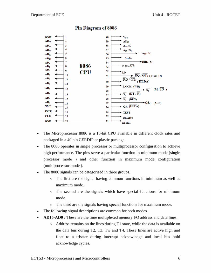
Department of ECE Unit 4 - RGCET
ECT53 - Microprocessors and Microcontrollers 9
The following pin functions are for the minimum mode operation of 8086
MIO ndash MemoryIO This is a status line logically equivalent to S2 in maximum
mode When it is low it indicates the CPU is having an IO operation and when it
is high it indicates that the CPU is having a memory operation This line becomes
active high in the previous T4 and remains active till final T4 of the current cycle
It is tristated during local bus ldquohold acknowledge ldquo
INTA ndash Interrupt Acknowledge This signal is used as a read strobe for
interrupt acknowledge cycles ie when it goes low the processor has accepted
the interrupt
ALE ndash Address Latch Enable This output signal indicates the availability of
the valid address on the addressdata lines and is connected to latch enable input
of latches This signal is active high and is never tristated
DTR ndash Data TransmitReceive This output is used to decide the direction of
data flow through the transreceivers (bidirectional buffers) When the processor
Department of ECE Unit 4 - RGCET
ECT53 - Microprocessors and Microcontrollers 10
sends out data this signal is high and when the processor is receiving data this
signal is low
DEN ndash Data Enable This signal indicates the availability of valid data over the
addressdata lines It is used to enable the transreceivers ( bidirectional buffers ) to
separate the data from the multiplexed addressdata signal It is active from the
middle of T2 until the middle of T4 This is tristated during lsquo hold acknowledgersquo
cycle
HOLD HLDA- Acknowledge When the HOLD line goes high it indicates to
the processor that another master is requesting the bus access The processor after
receiving the HOLD request issues the hold acknowledge signal on HLDA pin in
the middle of the next clock cycle after completing the current bus cycle
At the same time the processor floats the local bus and control lines When the
processor detects the HOLD line low it lowers the HLDA signal HOLD is an
asynchronous input and is should be externally synchronized If the DMA request
is made while the CPU is performing a memory or IO cycle it will release the
local bus during T4 provided
1The request occurs on or before T2 state of the current cycle
2The current cycle is not operating over the lower byte of a word
3The current cycle is not the first acknowledge of an interrupt acknowledge sequence
4 A Lock instruction is not being executed
The following pin functions are applicable for maximum mode operation of 8086
S2 S1 S0 ndash Status Lines These are the status lines which reflect the type of
operation being carried out by the processor These become activity during T4 of
the previous cycle and active during T1 and T2 of the current bus cycles
LOCK This output pin indicates that other system bus master will be prevented
fromgaining the system bus while the LOCK signal is low The LOCK signal is
activated by the lsquoLOCKrsquo prefix instruction and remains active until the
completion of the next instruction When the CPU is executing a critical
Department of ECE Unit 4 - RGCET
ECT53 - Microprocessors and Microcontrollers 11
instruction which requires the system bus the LOCK prefix instruction ensures
that other processors connected in the system will not gain the control of the bus
The 8086 while executing the prefixed instruction asserts the bus lock signal output
which may be connected to an external bus controller By prefetching the instruction
there is a considerable speeding up in instruction execution in 8086 This is known as
instruction pipelining
S2 S1 S0 Indication
0
0
0
0
1
1
1
1
0
0
1
1
0
0
1
1
0
1
0
1
0
1
0
1
Interrupt Acknowledge
Read IO port
Write IO port
Halt
Code Access
Read Memory
Write Memory
Passive
At the starting the CSIP is loaded with the required address from which the
execution is to be started Initially the queue will be empty an the microprocessor
starts a fetch operation to bring one byte (the first byte) of instruction code if the
CSIP address is odd or two bytes at a time if the CSIP address is even
The first byte is a complete opcode in case of some instruction (one byte opcode
instruction) and is a part of opcode in case of some instructions ( two byte opcode
instructions) the remaining part of code lie in second byte
The second byte is then decoded in continuation with the first byte to decide the
instruction length and the number of subsequent bytes to be treated as instruction
data The queue is updated after every byte is read from the queue but the fetch
cycle is initiated by BIU only if at least two bytes of the queue are empty and the
EU may be concurrently executing the fetched instructions
Department of ECE Unit 4 - RGCET
ECT53 - Microprocessors and Microcontrollers 12
The next byte after the instruction is completed is again the first opcode byte of
the next instruction A similar procedure is repeated till the complete execution of
the program The fetch operation of the next instruction is overlapped with the
execution of the current instruction As in the architecture there are two separate
units namely Execution unit and Bus interface unit
While the execution unit is busy in executing an instruction after it is completely
decoded the bus interface unit may be fetching the bytes of the next instruction
from memory depending upon the queue status
QS1 QS0 Indication
0
0
1
1
0
1
0
1
No Operation
First Byte of the opcode from the queue
Empty Queue
Subsequent Byte from the Queue
RQGT0 RQGT1 ndash RequestGrant These pins are used by the other local bus
master in maximum mode to force the processor to release the local bus at the
end of the processor current bus cycle
Each of the pin is bidirectional with RQGT0 having higher priority than
RQGT1 RQGT pins have internal pull-up resistors and may be left
unconnected RequestGrant sequence is as follows
1A pulse of one clock wide from another bus master requests the bus access to 8086
2During T4(current) or T1(next) clock cycle a pulse one clock wide from 8086 to the
requesting master indicates that the 8086 has allowed the local bus to float and that it
will enter the lsquohold acknowledgersquo state at next cycle The CPU bus interface unit is likely
to be disconnected from the local bus of the system
3A one clock wide pulse from the another master indicates to the 8086 that the hold
request is about to end and the 8086 may regain control of the local bus at the next clock
cycle Thus each master to master exchange of the local bus is a sequence of 3 pulses
There must be at least one dead clock cycle after each bus exchange The request and
grant pulses are active lowFor the bus request those are received while 8086 is
Department of ECE Unit 4 - RGCET
ECT53 - Microprocessors and Microcontrollers 13
performing memory or IO cycle the granting of the bus is governed by the rules as in
case of HOLD and HLDA in minimum mode
33 Maximum Mode 8086 System
In the maximum mode the 8086 is operated by strapping the MNMX pin to
ground
In this mode the processor derives the status signal S2 S1 S0 Another chip
called bus controller derives the control signal using this status information
In the maximum mode there may be more than one microprocessor in the system
configuration
The components in the system are same as in the minimum mode system
The basic function of the bus controller chip IC8288 is to derive control signals
like RD and WR ( for memory and IO devices) DEN DTR ALE etc using the
information by the processor on the status lines
The bus controller chip has input lines S2 S1 S0 and CLK These inputs to 8288
are driven by CPU
It derives the outputs ALE DEN DTR MRDC MWTC AMWC IORC IOWC
and AIOWC The AEN IOB and CEN pins are specially useful for
multiprocessor systems
Department of ECE Unit 4 - RGCET
ECT53 - Microprocessors and Microcontrollers 14
AEN and IOB are generally grounded CEN pin is usually tied to +5V The
significance of the MCEPDEN output depends upon the status of the IOB pin
If IOB is grounded it acts as master cascade enable to control cascade 8259A
else it acts as peripheral data enable used in the multiple bus configurations
INTA pin used to issue two interrupt acknowledge pulses to the interrupt
controller or to an interrupting device
IORC IOWC are IO read command and IO write command signals respectively
These signals enable an IO interface to read or write the data from or to the
address port
The MRDC MWTC are memory read command and memory write command
signals respectively and may be used as memory read or write signals
All these command signals instructs the memory to accept or send data from or to
the bus
For both of these write command signals the advanced signals namely AIOWC
and AMWTC are available
Department of ECE Unit 4 - RGCET
ECT53 - Microprocessors and Microcontrollers 15
Here the only difference between in timing diagram between minimum mode and
maximum mode is the status signals used and the available control and advanced
command signals
R0 S1 S2 are set at the beginning of bus cycle8288 bus controller will output a
pulse as on the ALE and apply a required signal to its DT R pin during T1
In T2 8288 will set DEN=1 thus enabling transceivers and for an input it will
activate MRDC or IORC These signals are activated until T4 For an output the
AMWC or AIOWC is activated from T2 to T4 and MWTC or IOWC is activated
from T3 to T4
The status bit S0 to S2 remains active until T3 and become passive during T3 and
T4
If reader input is not activated before T3 wait state will be inserted between T3
and T4
34 Minimum Mode 8086 System
In a minimum mode 8086 system the microprocessor 8086 is operated in
minimum mode by strapping its MNMX pin to logic 1
In this mode all the control signals are given out by the microprocessor chip
itselfThere is a single microprocessor in the minimum mode system
The remaining components in the system are latches transreceivers clock
generator memory and IO devices Some type of chip selection logic may be
required for selecting memory or IO devices depending upon the address map of
the system
Latches are generally buffered output D-type flip-flops like 74LS373 or 8282
They are used for separating the valid address from the multiplexed addressdata
signals and are controlled by the ALE signal generated by 8086
Transreceivers are the bidirectional buffers and some times they are called as data
amplifiers They are required to separate the valid data from the time multiplexed
addressdata signals
They are controlled by two signals namely DEN and DTR
Department of ECE Unit 4 - RGCET
ECT53 - Microprocessors and Microcontrollers 16
The DEN signal indicates the direction of data ie from or to the processor The
system contains memory for the monitor and users program storage
Usually EPROM are used for monitor storage while RAM for users program
storage A system may contain IO devices
RQGT Timings in Maximum Mode
The requestgrant response sequence contains a series of three pulses The
requestgrant pins are checked at each rising pulse of clock input
When a request is detected and if the condition for HOLD request is satisfied the
processor issues a grant pulse over the RQGT pin immediately during T4
(current) or T1 (next) state
When the requesting master receives this pulse it accepts the control of the bus it
sends a release pulse to the processor using RQGT pin
Maximum Mode Interface
When the 8086 is set for the maximum-mode configuration it provides signals for
implementing a multiprocessor coprocessor system environment
By multiprocessor environment we mean that one microprocessor exists in the
system and that each processor is executing its own program
Usually in this type of system environment there are some system resources that
are common to all processorsThey are called as global resources There are also
Department of ECE Unit 4 - RGCET
ECT53 - Microprocessors and Microcontrollers 17
other resources that are assigned to specific processors These are known as local
or private resources
Coprocessor also means that there is a second processor in the system In this two
processor does not access the bus at the same time One passes the control of the
system bus to the other and then may suspend its operation
In the maximum-mode 8086 system facilities are provided for implementing
allocation of global resources and passing bus control to other microprocessor or
coprocessor
8288 Bus Controller ndash Bus Command and Control Signals
8086 does not directly provide all the signals that are required to control the
memory IO and interrupt interfaces
Department of ECE Unit 4 - RGCET
ECT53 - Microprocessors and Microcontrollers 18
Specially the WR MIO DTR DEN ALE and INTA signals are no longer
produced by the 8086 Instead it outputs three status signals S0 S1 S2 prior to the
initiation of each bus cycle This 3- bit bus status code identifies which type of
bus cycle is to follow
S2S1S0 are input to the external bus controller device the bus controller
generates the appropriately timed command and control signals
S2 S1 S0 Indication 8288 Command
0
0
0
0
1
1
1
1
0
0
1
1
0
0
1
1
0
1
0
1
0
1
0
1
Interrupt Acknowledge
Read IO port
Write IO port
Halt
Instruction Fetch
Read Memory
Write Memory
Passive
INTA
IORC
IOWC AIOWC
None
MRDC
MRDC
MWTC AMWC
None
The 8288 produces one or two of these eight command signals for each bus
cycles For instance when the 8086 outputs the code S2S1S0 equals 001 it
indicates that an IO read cycle is to be performed
In the code 111 is output by the 8086 it is signaling that no bus activity is to take
place
The control outputs produced by the 8288 are DEN DTR and ALE These 3
signals provide the same functions as those described for the minimum system
mode This set of bus commands and control signals is compatible with the
Multibus and industry standard for interfacing microprocessor systems
The output of 8289 are bus arbitration signals
Bus busy (BUSY) common bus request (CBRQ) bus priority out (BPRO) bus
priority in (BPRN) bus request (BREQ) and bus clock (BCLK)
Department of ECE Unit 4 - RGCET
ECT53 - Microprocessors and Microcontrollers 19
They correspond to the bus exchange signals of the Multibus and are used to lock
other processor off the system bus during the execution of an instruction by the
8086
In this way the processor can be assured of uninterrupted access to common
system resources such as global memory
Queue Status Signals Two new signals that are produced by the 8086 in the
maximum-mode system are queue status outputs QS0 and QS1 Together they
form a 2-bit ueue status code QS1QS0
Following table shows the four different queue status
QS1 QS0 Queue Status
0 (low) 0 Queue Empty The queue has been reinitialized as a
result of the execution of a transfer instruction
0 1 First Byte The byte taken from the queue was the first
byte of the instruction
1 0 Queue Empty The queue has been reinitialized as a
result of the execution of a transfer instruction
1 1 Subsequent Byte The byte taken from the queue was a
subsequent byte of the instruction
Table - Queue status codes
Local Bus Control Signal ndash Request Grant Signals In a maximum mode
configuration the minimum mode HOLD HLDA interface is also changed
These two are replaced by requestgrant lines RQ GT0 and RQ GT1
respectively They provide a prioritized bus access mechanism for accessing the
local bus
Department of ECE Unit 4 - RGCET
ECT53 - Microprocessors and Microcontrollers 20
Memory Read Timing Diagram in Maximum Mode of 8086
Memory Write Timing in Maximum mode of 8086
Department of ECE Unit 4 - RGCET
ECT53 - Microprocessors and Microcontrollers 21
Minimum Mode Interface
When the Minimum mode operation is selected the 8086 provides all control
signals needed to implement the memory and IO interface
The minimum mode signal can be divided into the following basic groups
1 Addressdata bus
2 Status
3 Control
4 Interrupt and
5 DMA
Each and every group is explained clearly
AddressData Bus
These lines serve two functions As an address bus is 20 bits long and consists of
signal lines A0 through A19 A19 represents the MSB and A0 LSB A 20bit
address gives the 8086 a 1Mbyte memory address space More over it has an
independent IO address space which is 64K bytes in length
The 16 data bus lines D0 through D15 are actually multiplexed with address lines
A0 through A15 respectively By multiplexed we mean that the bus work as an
address bus during first machine cycle and as a data bus during next machine
cycles
D15 is the MSB and D0 LSB When acting as a data bus they carry readwrite
data for memory inputoutput data for IO devices and interrupt type codes from
an interrupt controller
Department of ECE Unit 4 - RGCET
ECT53 - Microprocessors and Microcontrollers 22
Status signal
The four most significant address lines A19 through A16 are also multiplexed but
in this case with status signals S6 through S3 These status bits are output on the
bus at the same time that data are transferred over the other bus lines
Bit S4 and S3 together from a 2 bit binary code that identifies which of the 8086
internal segment registers are used to generate the physical address that was
output on the address bus during the current bus cycleCode S4S3 = 00 identifies
a register known as extra segment register as the source of the segment address
Status line S5 reflects the status of another internal characteristic of the 8086 It is
the logic level of the internal enable flag The last status bit S6 is always at the
logic 0 level
S4 S3 Segment Register
0
0
0
1
Extra
Stack
Department of ECE Unit 4 - RGCET
ECT53 - Microprocessors and Microcontrollers 23
1
1
0
1
Code none
Data
Memory segment status codes
Control Signals
The control signals are provided to support the 8086 memory IO interfaces They
control functions such as when the bus is to carry a valid address in which
direction data are to be transferred over the bus when valid write data are on the
bus and when to put read data on the system bus
ALE is a pulse to logic 1 that signals external circuitry when a valid address word
is on the bus This address must be latched in external circuitry on the 1-to-0 edge
of the pulse at ALE
Another control signal that is produced during the bus cycle is BHE bank high
enable Logic 0 on this used as a memory enable signal for the most significant
byte half of the data bus D8 through D1 These lines also serves a second
function which is as the S7 status line
Using the MIO and DTR lines the 8086 signals which type of bus cycle is in
progress and in which direction data are to be transferred over the bus The logic
level of MIO tells external circuitry whether a memory or IO transfer is taking
place over the bus Logic 1 at this output signals a memory operation and logic 0
an IO operation
The direction of data transfer over the bus is signaled by the logic level output at
DTR When this line is logic 1 during the data transfer part of a bus cycle the
bus is in the transmit mode Therefore data are either written into memory or
output to an IO device On the other hand logic 0 at DTR signals that the bus is
in the receive mode This corresponds to reading data from memory or input of
data from an input port
Department of ECE Unit 4 - RGCET
ECT53 - Microprocessors and Microcontrollers 24
The signal read RD and write WR indicates that a read bus cycle or a write bus
cycle is in progress The 8086 switches WR to logic 0 to signal external device
that valid write or output data are on the bus
On the other hand RD indicates that the 8086 is performing a read of data of the
bus During read operations one other control signal is also supplied This is DEN
( data enable) and it signals external devices when they should put data on the
bus There is one other control signal that is involved with the memory and IO
interface This is the READY signal
READY signal is used to insert wait states into the bus cycle such that it is
extended by a number of clock periods This signal is provided by an external
clock generator device and can be supplied by the memory or IO sub-system to
signal the 8086 when they are ready to permit the data transfer to be completed
Interrupt signals
The key interrupt interface signals are interrupt request (INTR) and interrupt
acknowledge ( INTA)
INTR is an input to the 8086 that can be used by an external device to signal that
it need to be serviced
Logic 1 at INTR represents an active interrupt request When an interrupt request
has been recognized by the 8086 it indicates this fact to external circuit with
pulse to logic 0 at the INTA output
The TEST input is also related to the external interrupt interface Execution of a
WAIT instruction causes the 8086 to check the logic level at the TEST input
If the logic 1 is found the MPU suspend operation and goes into the idle state
The 8086 no longer executes instructions instead it repeatedly checks the logic
level of the TEST input waiting for its transition back to logic 0
As TEST switches to 0 execution resume with the next instruction in the
program This feature can be used to synchronize the operation of the 8086 to an
event in external hardware
There are two more inputs in the interrupt interface the nonmaskable interrupt
NMI and the reset interrupt RESET
Department of ECE Unit 4 - RGCET
ECT53 - Microprocessors and Microcontrollers 25
On the 0-to-1 transition of NMI control is passed to a nonmaskable interrupt
service routine The RESET input is used to provide a hardware reset for the
8086 Switching RESET to logic 0 initializes the internal register of the 8086 and
initiates a reset service routine
DMA Interface signals
The direct memory access DMA interface of the 8086 minimum mode consist of
the HOLD and HLDA signals
When an external device wants to take control of the system bus it signals to the
8086 by switching HOLD to the logic 1 level At the completion of the current
bus cycle the 8086 enters the hold state In the hold state signal lines AD0
through AD15 A16S3 through A19S6 BHE MIO DTR RD WR DEN and
INTR are all in the high Z state
The 8086 signals external device that it is in this state by switching its HLDA
output to logic 1 level
General Bus Operation
The 8086 has a combined address and data bus commonly referred as a time
multiplexed address and data bus
The main reason behind multiplexing address and data over the same pins is the
maximum utilisation of processor pins and it facilitates the use of 40 pin standard
DIP package
The bus can be demultiplexed using a few latches and transreceivers when ever
required
Basically all the processor bus cycles consist of at least four clock cycles These
are referred to as T1 T2 T3 T4 The address is transmitted by the processor
during T1 It is present on the bus only for one cycle
The negative edge of this ALE pulse is used to separate the address and the data
or status information In maximum mode the status lines S0 S1 and S2 are used
to indicate the type of operation
Status bits S3 to S7 are multiplexed with higher order address bits and the BHE
signal Address is valid during T1 while status bits S3 to S7 are valid during T2
through T4
Department of ECE Unit 4 - RGCET
ECT53 - Microprocessors and Microcontrollers 26
Maximum mode
In the maximum mode the 8086 is operated by strapping the MNMX pin to
ground
In this mode the processor derives the status signal S2 S1 S0 Another chip
called bus controller derives the control signal using this status information
In the maximum mode there may be more than one microprocessor in the system
configuration
Minimum mode
In a minimum mode 8086 system the microprocessor 8086 is operated in
minimum mode by strapping its MNMX pin to logic 1
In this mode all the control signals are given out by the microprocessor chip
itself
There is a single microprocessor in the minimum mode system
Bus Request and Bus Grant Timings in Minimum Mode System of 8086
Department of ECE Unit 4 - RGCET
ECT53 - Microprocessors and Microcontrollers 27
Hold Response sequence The HOLD pin is checked at leading edge of each clock
pulse If it is received active by the processor before T4 of the previous cycle or
during T1 state of the current cycle the CPU activates HLDA in the next clock
cycle and for succeeding bus cycles the bus will be given to another requesting
master
The control of the bus is not regained by the processor until the requesting master
does not drop the HOLD pin low When the request is dropped by the requesting
master the HLDA is dropped by the processor at the trailing edge of the next
clock
Write Cycle Timing Diagram for Minimum Mode
The working of the minimum mode configuration system can be better described
in terms of the timing diagrams rather than qualitatively describing the operations
The opcode fetch and read cycles are similar Hence the timing diagram can be
categorized in two parts the first is the timing diagram for read cycle and the
second is the timing diagram for write cycle
Department of ECE Unit 4 - RGCET
ECT53 - Microprocessors and Microcontrollers 28
The read cycle begins in T1 with the assertion of address latch enable (ALE)
signal and also M IO signal During the negative going edge of this signal the
valid address is latched on the local bus
The BHE and A0 signals address low high or both bytes From T1 to T4 the
MIO signal indicates a memory or IO operation
At T2 the address is removed from the local bus and is sent to the output The bus
is then tristated The read (RD) control signal is also activated in T2
The read (RD) signal causes the address device to enable its data bus drivers
After RD goes low the valid data is available on the data bus
The addressed device will drive the READY line high When the processor
returns the read signal to high level the addressed device will again tristate its bus
drivers
A write cycle also begins with the assertion of ALE and the emission of the
address The MIO signal is again asserted to indicate a memory or IO operation
Department of ECE Unit 4 - RGCET
ECT53 - Microprocessors and Microcontrollers 29
In T2 after sending the address in T1 the processor sends the data to be written to
the addressed location
The data remains on the bus until middle of T4 state The WR becomes active at
the beginning of T2 (unlike RD is somewhat delayed in T2 to provide time for
floating)
The BHE and A0 signals are used to select the proper byte or bytes of memory or
IO word to be read or write
The MIO RD and WR signals indicate the type of data transfer as specified in
table below
35 Addressing Modes of 8086
Definition An instruction acts on any number of operandsThe way an instruction
accesses its operands is called its Addressing modes
Operands may be of three types
o Implicit
o Explicit
o Both Implicit and Explicit
Implicit operands mean that the instruction by definition has some specific operands
The programmers do NOT select these operands
Example Implicit operands
XLAT automatically takes AL and BX as
operands
AAM it operates on the contents of AX
Explicit operands mean the instruction operates on the operands specified by the
programmer
Example Explicit operands
MOV AX BX it takes AX and BX as
Department of ECE Unit 4 - RGCET
ECT53 - Microprocessors and Microcontrollers 30
operands
XCHG SI DI it takes SI and DI as operands
Implicit and explicit operands
Example ImplicitExplicit operands
MUL BX automatically multiply BX explicitly times
AX
The location of an operand value in memory space is called the Effective Address (EA)
We can classify the addressing modes of 8086 into four groups
Immediate addressing
Register addressing
Memory addressing
IO port addressing
The first three Addresssing modes are clearly explained
Immediate addressing mode amp Register addressing mode
Immediate Addressing Mode
In this addressing mode the operand is stored as part of the instruction The immediate
operand which is stored along with the instruction resides in the code segment -- not in
the data segment This addressing mode is also faster to execute an instruction because
the operand is read with the instruction from memory Here are some examples
Example Immediate Operands
MOV AL 20 move the constant 20 into register AL
ADD AX 5 add constant 5 to register EAX
MOV DX offset msg move the address of message to
register DX
Register addressing mode
In this addressing mode the operands may be
Department of ECE Unit 4 - RGCET
ECT53 - Microprocessors and Microcontrollers 31
reg16 16-bit general registers AX BX CX DX SI DI SP or BP
reg8 8-bit general registers AH BH CH DH AL BL CL or DL
Sreg segment registers CS DS ES or SS There is an exception CS cannot be
a destination
For register addressing modes there is no need to compute the effective address The
operand is in a register and to get the operand there is no memory access involved
Example Register Operands
MOV AX BX mov reg16 reg16
ADD AX SI add reg16 reg16
MOV DS AX mov Sreg reg16
Some rules in register addressing modes
1 You may not specify CS as the destination operand
Example mov CS 02h ndashgt wrong
2 Only one of the operands can be a segment register You cannot move data from one
segment register to another with a single mov instruction To copy the value of cs to ds
you would have to use some sequence like
mov dscs -gt wrong
mov ax cs
mov ds ax -gt the way we do it
You should never use the segment registers as data registers to hold arbitrary values
They should only contain segment addresses
Memory Addressing Modes
Memory (RAM) is the main component of a computer to store temporary data and
machine instructions In a program programmers many times need to read from and
write into memory locations
There are different forms of memory addressing modes
Department of ECE Unit 4 - RGCET
ECT53 - Microprocessors and Microcontrollers 32
1 Direct Addressing
2 Register indirect addressing
3 Based addressing
4 Indexed addressing
5 Based indexed addressing
6 Based indexed with displacement
Direct Addressing Mode amp Register Indirect Addressing Mode
Direct Addressing Mode
The instruction mov alds[8088h] loads the AL register with a copy of the byte at
memory location 8088h Likewise the instruction mov ds[1234h]dl stores the value in
the dl register to memory location 1234h By default all displacement-only values
provide offsets into the data segment If you want to provide an offset into a different
segment you must use a segment override prefix before your address For example to
access location 1234h in the extra segment (es) you would use an instruction of the form
mov axes[1234h] Likewise to access this location in the code segment you would use
the instruction mov ax cs[1234h] The ds prefix in the previous examples is not a
segment override
Department of ECE Unit 4 - RGCET
ECT53 - Microprocessors and Microcontrollers 33
The instruction mov alds[8088h] is same as mov al [8088h] If not mentioned DS
register is taken by default
Register Indirect Addressing Mode
The 80x86 CPUs let you access memory indirectly through a register using the register
indirect addressing modes There are four forms of this addressing mode on the 8086
best demonstrated by the following instructions
mov al [bx]
mov al [bp]
mov al [si]
mov al [di]
Code Example
MOV BX 100H
MOV AL [BX]
The [bx] [si] and [di] modes use the ds segment by default The [bp] addressing mode
uses the stack segment (ss) by default You can use the segment override prefix symbols
if you wish to access data in different segments The following instructions demonstrate
the use of these overrides
mov al cs[bx]
mov al ds[bp]
mov al ss[si]
mov al es[di]
Intel refers to [bx] and [bp] as base addressing modes and bx and bp as base registers (in
fact bp stands for base pointer) Intel refers to the [si] and [di] addressing modes as
indexed addressing modes (si stands for source index di stands for destination index)
However these addressing modes are functionally equivalent This text will call these
forms register indirect modes to be consistent
Department of ECE Unit 4 - RGCET
ECT53 - Microprocessors and Microcontrollers 34
Based Addressing Mode and Indexed Addressing Modes
Based Addressing Mode
8-bit or 16-bit instruction operand is added to the contents of a base register (BX or BP)
the resulting value is a pointer to location where data resides
Mov al [bx][si]
Mov bl [bp][di]
Mov cl [bp][di]
Code Example
If bx=1000h
si=0880h
Mov AL [1000+880]
Mov AL[1880]
Indexed Addressing Modes
The indexed addressing modes use the following syntax
mov al [bx+disp]
mov al [bp+disp]
mov al [si+disp]
mov al [di+disp]
Code Example
MOV BX 100H
MOV AL [BX + 15]
MOV AL [BX + 16]
If bx contains 1000h then the instruction mov cl [bx+20h] will load cl from memory
location ds1020h Likewise if bp contains 2020h mov dh [bp+1000h] will load dh from
location ss3020 The offsets generated by these addressing modes are the sum of the
constant and the specified register The addressing modes involving bx si and di all use
Department of ECE Unit 4 - RGCET
ECT53 - Microprocessors and Microcontrollers 35
the data segment the [bp+disp] addressing mode uses the stack segment by default As
with the register indirect addressing modes you can use the segment override prefixes to
specify a different segment
mov al ss[bx+disp]
mov al es[bp+disp]
mov al cs[si+disp]
mov al ss[di+disp]
Based Indexed Addressing Modes amp Based Indexed Plus Displacement Addressing Mode
Based Indexed Addressing Modes
The based indexed addressing modes are simply combinations of the register indirect
addressing modes These addressing modes form the offset by adding together a base
register (bx or bp) and an index register (si or di) The allowable forms for these
addressing modes are
mov al [bx+si]
mov al [bx+di]
mov al [bp+si]
mov al [bp+di]
Code Example
MOV BX 100H
MOV SI 200H
MOV AL [BX + SI]
INC BX
INC SI
Department of ECE Unit 4 - RGCET
ECT53 - Microprocessors and Microcontrollers 36
Suppose that bx contains 1000h and si contains 880h Then the instruction mov al[bx][si]
would load al from location DS1880h Likewise if bp contains 1598h and di contains
1004 mov ax[bp+di] will load the 16 bits in ax from locations SS259C and SS259D
The addressing modes that do not involve bp use the data segment by default Those that
have bp as an operand use the stack segment by default
Based Indexed Plus Displacement Addressing Mode
These addressing modes are a slight modification of the baseindexed addressing modes
with the addition of an eight bit or sixteen bit constant The following are some examples
of these addressing modes
mov al disp[bx][si]
mov al disp[bx+di]
mov al [bp+si+disp]
mov al [bp][di][disp]
Department of ECE Unit 4 - RGCET
ECT53 - Microprocessors and Microcontrollers 37
Code Example
MOV BX 100H
MOV SI 200H
MOV AL [BX + SI +100H]
INC BX
INC SI
Index or Pointer Registers
These registers can also be called as Special Purpose registers
Department of ECE Unit 4 - RGCET
ECT53 - Microprocessors and Microcontrollers 38
Stack Pointer (SP) is a 16-bit register pointing to program stack ie it is used to hold the
address of the top of stack The stack is maintained as a LIFO with its bottom at the start
of the stack segment (specified by the SS segment register)Unlike the SP register the BP
can be used to specify the offset of other program segments
Base Pointer (BP) is a 16-bit register pointing to data in stack segment It is usually used
by subroutines to locate variables that were passed on the stack by a calling program BP
register is usually used for based based indexed or register indirect addressing
Source Index (SI) is a 16-bit register SI is used for indexed based indexed and register
indirect addressing as well as a source data address in string manipulation instructions
Used in conjunction with the DS register to point to data locations in the data segment
Destination Index (DI) is a 16-bit register Used in conjunction with the ES register in
string operations DI is used for indexed based indexed and register indirect addressing
as well as a destination data address in string manipulation instructions In short
Destination Index and SI Source Index registers are used to hold address
Segment Registers
Most of the registers contain datainstruction offsets within 64 KB memory segment
There are four different 64 KB segments for instructions stack data and extra data To
specify where in 1 MB of processor memory these 4 segments are located the processor
uses four segment registers
Department of ECE Unit 4 - RGCET
ECT53 - Microprocessors and Microcontrollers 39
Code segment (CS) is a 16-bit register containing address of 64 KB segment with
processor instructions The processor uses CS segment for all accesses to instructions
referenced by instruction pointer (IP) register CS register cannot be changed directly
The CS register is automatically updated during far jump far call and far return
instructions
Stack segment (SS) is a 16-bit register containing address of 64KB segment with
program stack By default the processor assumes that all data referenced by the stack
pointer (SP) and base pointer (BP) registers is located in the stack segment SS register
can be changed directly using POP instruction
Data segment (DS) is a 16-bit register containing address of 64KB segment with
program data By default the processor assumes that all data referenced by general
registers (AX BX CX DX) and index register (SI DI) is located in the data segment
DS register can be changed directly using POP and LDS instructions
Extra segment (ES) used to hold the starting address of Extra segment Extra segment is
provided for programs that need to access a second data segment Segment registers
cannot be used in arithmetic operations
Other registers of 8086
Instruction Pointer (IP) is a 16-bit register This is a crucially important register which
is used to control which instruction the CPU executes The ip or program counter is used
to store the memory location of the next instruction to be executed The CPU checks the
program counter to ascertain which instruction to carry out next It then updates the
program counter to point to the next instruction Thus the program counter will always
point to the next instruction to be executed
Flag Register contains a group of status bits called flags that indicate the status of the
CPU or the result of arithmetic operations There are two types of flags
Department of ECE Unit 4 - RGCET
ECT53 - Microprocessors and Microcontrollers 40
1 The status flags which reflect the result of executing an instruction The programmer
cannot setreset these flags directly
2 The control flags enable or disable certain CPU operations The programmer can
setreset these bits to control the CPUs operation
Nine individual bits of the status register are used as control flags (3 of them) and status
flags (6 of them)The remaining 7 are not used
A flag can only take on the values 0 and 1 We say a flag is set if it has the value 1The
status flags are used to record specific characteristics of arithmetic and of logical
instructions
Control Flags There are three control flags
1 The Direction Flag (D) Affects the direction of moving data blocks by such
instructions as MOVS CMPS and SCAS The flag values are 0 = up and 1 = down and
can be setreset by the STD (set D) and CLD (clear D) instructions
2 The Interrupt Flag (I) Dictates whether or not system interrupts can occur Interrupts
are actions initiated by hardware block such as input devices that will interrupt the
normal execution of programs The flag values are 0 = disable interrupts or 1 = enable
interrupts and can be manipulated by the CLI (clear I) and STI (set I) instructions
Department of ECE Unit 4 - RGCET
ECT53 - Microprocessors and Microcontrollers 41
3 The Trap Flag (T) Determines whether or not the CPU is halted after the execution
of each instruction When this flag is set (ie = 1) the programmer can single step
through his program to debug any errors When this flag = 0 this feature is off This flag
can be set by the INT 3 instruction
Status Flags There are six status flags
1 The Carry Flag (C) This flag is set when the result of an unsigned arithmetic
operation is too large to fit in the destination register This happens when there is an end
carry in an addition operation or there an end borrows in a subtraction operation A value
of 1 = carry and 0 = no carry
2 The Overflow Flag (O) This flag is set when the result of a signed arithmetic
operation is too large to fit in the destination register (ie when an overflow occurs)
Overflow can occur when adding two numbers with the same sign (ie both positive or
both negative) A value of 1 = overflow and 0 = no overflow
3 The Sign Flag (S) This flag is set when the result of an arithmetic or logic operation
is negative This flag is a copy of the MSB of the result (ie the sign bit) A value of 1
means negative and 0 = positive
4 The Zero Flag (Z) This flag is set when the result of an arithmetic or logic operation
is equal to zero A value of 1 means the result is zero and a value of 0 means the result is
not zero
5 The Auxiliary Carry Flag (A) This flag is set when an operation causes a carry from
bit 3 to bit 4 (or a borrow from bit 4 to bit 3) of an operand A value of 1 = carry and 0 =
no carry
6 The Parity Flag (P) This flags reflects the number of 1s in the result of an operation
If the number of 1s is even its value = 1 and if the number of 1s is odd then its value = 0
36 8086 Instruction Set and its Classification
The instructions of 8086 are classified into SIX groups They are
1 DATA TRANSFER INSTRUCTIONS
Department of ECE Unit 4 - RGCET
ECT53 - Microprocessors and Microcontrollers 42
2 ARITHMETIC INSTRUCTIONS
3 BIT MANIPULATION INSTRUCTIONS
4 STRING INSTRUCTIONS
5 PROGRAM EXECUTION TRANSFER INSTRUCTIONS
6 PROCESS CONTROL INSTRUCTIONS
1DATA TRANSFER INSTRUCTIONS
The DATA TRANSFER INSTRUCTIONS are those which transfers the DATA from
any one source to any one destinationThe datas may be of any type They are again
classified into four groupsThey are
GENERAL ndash PURPOSE
BYTE OR WORD
TRANSFER INSTRUCTIONS
SIMPLE INPUT AND
OUTPUT PORT
TRANSFER
INSTRUCTION
SPECIAL ADDRESS
TRANSFER
INSTRUCTION
FLAG
TRANSFER
INSTRUCTIONS
MOV
PUSH
POP
XCHG
XLAT
IN
OUT
LEA
LDS
LES
LAHF
SAHF
PUSHF
POPF
2ARITHMETIC INSTRUCTIONS
These instructions are those which are useful to perform Arithmetic calculations such as
addition subtraction multiplication and divisionThey are again classified into four
groupsThey are
ADDITION
INSTRUCTIONS
SUBTRACTION
INSTRUCTIONS
MULTIPLICATION
INSTRUCTIONS
DIVISION
INSTRUCTIONS
ADD
ADC
INC
AAA
DAA
SUB
SBB
DEC
NEG
CMP
AAS
DAS
MUL
IMUL
AAM
DIV
IDIV
AAD
CBW
CWD
3BIT MANIPULATION INSTRUCTIONS
Department of ECE Unit 4 - RGCET
ECT53 - Microprocessors and Microcontrollers 43
These instructions are used to perform Bit wise operations
LOGICAL INSTRUCTIONS SHIFT INSTRUCTIONS ROTATE INSTRUCTIONS
NOT
AND
OR
XOR
TEST
SHL SAL
SHR
SAR
ROL
ROR
RCL
RCR
4 STRING INSTRUCTIONS
The string instructions function easily on blocks of memoryThey are user friendly
instructions which help for easy program writing and execution They can speed up the
manipulating codeThey are useful in array handling tables and records
STRING INSTRUCTIONS
REP
REPE REPZ
REPNE REPNZ
MOVS MOVSB MOVSW
COMPS COMPSB
COMPSW
SCAS SCASB SCASW
LODS LODSB LODSW
STOS STOSB STOSW
5PROGRAM EXECUTION TRANSFER INSTRUCTIONS
These instructions transfer the program control from one address to other address ( Not
in a sequence) They are again classified into four groupsThey are
UNCONDITIONAL
TRANSFER
INSTRUCTIONS
CONDITIONAL
TRANSFER
INSTRUCTIONS
ITERATION CONTROL
INSTRUCTIONS
INTERRUPT
INSTRUCTIONS
CALL
RET
JMP
JA JNBE
JAE JNB
JB JNAE
JBE JNA
JC
JE JZ
JLE JNG
JNC
JNE JNZ
JNO
JNP JPO
JNS
LOOP
LOOPE LOOPZ
LOOPNE LOOPNZ
JCXZ
INT
INTO
IRET
Department of ECE Unit 4 - RGCET
ECT53 - Microprocessors and Microcontrollers 44
JG JNLE
JGE JNL
JL JNGE
JO
JP JPE
JS
6PROCESS CONTROL INSTRUCTIONS
These instructions are used to change the process of the Microprocessor They change the
process with the stored information They are again classified into Two groupsThey are
FLAG SET CLEAR
INSTRUCTIONS
EXTERNAL HARDWARE
SYNCHRONIZATION
INSTRUCTIONS
STC
CLC
CMC
STD
CLD
STI
CLI
HLT
WAIT
ESC
LOCK
NOP
37 Interrupts
Definition The meaning of lsquointerruptsrsquo is to break the sequence of operationWhile the
cpu is executing a programon lsquointerruptrsquo breaks the normal sequence of execution of
instructions diverts its execution to some other program called Interrupt Service Routine
(ISR)After executing ISR the control is transferred back again to the main
programInterrupt processing is an alternative to polling
Need for Interrupt Interrupts are particularly useful when interfacing IO devices that
provide or require data at relatively low data transfer rate
Types of Interrupts There are two types of Interrupts in 8086 They are
(i)Hardware Interrupts and
(ii)Software Interrupts
Department of ECE Unit 4 - RGCET
ECT53 - Microprocessors and Microcontrollers 45
(i) Hardware Interrupts (External Interrupts) The Intel microprocessors support
hardware interrupts through
Two pins that allow interrupt requests INTR and NMI
One pin that acknowledges INTA the interrupt requested on INTR
INTR and NMI
INTR is a maskable hardware interrupt The interrupt can be enableddisabled
using STICLI instructions or using more complicated method of updating the
FLAGS register with the help of the POPF instruction
When an interrupt occurs the processor stores FLAGS register into stack
disables further interrupts fetches from the bus one byte representing interrupt
type and jumps to interrupt processing routine address of which is stored in
location 4 ltinterrupt typegt Interrupt processing routine should return with the
IRET instruction
NMI is a non-maskable interrupt Interrupt is processed in the same way as the
INTR interrupt Interrupt type of the NMI is 2 ie the address of the NMI
processing routine is stored in location 0008h This interrupt has higher priority
than the maskable interrupt
ndash Ex NMI INTR
(ii) Software Interrupts (Internal Interrupts and Instructions) Software interrupts can
be caused by
INT instruction - breakpoint interrupt This is a type 3 interrupt
INT ltinterrupt numbergt instruction - any one interrupt from available 256
interrupts
INTO instruction - interrupt on overflow
Single-step interrupt - generated if the TF flag is set This is a type 1 interrupt
When the CPU processes this interrupt it clears TF flag before calling the
interrupt processing routine
Processor exceptions Divide Error (Type 0) Unused Opcode (type 6) and Escape
opcode (type 7)
Software interrupt processing is the same as for the hardware interrupts
Department of ECE Unit 4 - RGCET
ECT53 - Microprocessors and Microcontrollers 46
- Ex INT n (Software Instructions)
Control is provided through
o IF and TF flag bits
o IRET and IRETD
Performance of Hardware Interrupts
NMI Non maskable interrupts - TYPE 2 Interrupt
INTR Interrupt request - Between 20H and FFH
Interrupt Priority Structure
Performance of Software Interrupts
1 It decrements SP by 2 and pushes the flag register on the stack
2 Disables INTR by clearing the IF
3 It resets the TF in the flag Register
5 It decrements SP by 2 and pushes CS on the stack
Department of ECE Unit 4 - RGCET
ECT53 - Microprocessors and Microcontrollers 47
6 It decrements SP by 2 and pushes IP on the stack
6 Fetch the ISR address from the interrupt vector table
38 Other microprocessors the 80286 80386 and 80486 1048766 80286 Intel introduced 80286 in 1982
bull With 16-bit internal and external data bus
bull 24-bit address bus (224 = 16 megabyte)
bull virtual memory a way of fooling the microprocessor into thinking that it has access to
unlimited
memory by swapping data between disk storage and RAM
bull Real mode (faster operation with maximum of 1 Mbytes of memory) vs Protected
mode
protecting the operating system for accidental or deliberate destruction of the user
Protected
mode is slower but can use 16 Mbytes of memory
1048766 80386 introduced in 1985 also known as (80386DX)
bull With 32-bit internal and external data bus
bull 32-bit address bus (232 = 4 gigabyte-physical memory) With virtual memory 64
terabytes(246)
bull 80386SX was later introduced with the same internal structure with 16-bit external data
bus and
24-bit address bus 80386SX was much cheaper
1048766 All microprocessors discussed so far were general-purpose microprocessors and could
not handle
mathematical operations rapidly For this reason 8087 80287 80387 numeric data
processing chips
called math co-processors were used
1048766 80486 introduced in 1989 with 32-bit internal-external data bus and 32-bit address
bus
bull built in math co-processor in a single chip
bull Introduction of cache memory ( Static RAM with very fast access time)
Evolution of Intels Microprocessors
Department of ECE Unit 4 - RGCET
ECT53 - Microprocessors and Microcontrollers 10
sends out data this signal is high and when the processor is receiving data this
signal is low
DEN ndash Data Enable This signal indicates the availability of valid data over the
addressdata lines It is used to enable the transreceivers ( bidirectional buffers ) to
separate the data from the multiplexed addressdata signal It is active from the
middle of T2 until the middle of T4 This is tristated during lsquo hold acknowledgersquo
cycle
HOLD HLDA- Acknowledge When the HOLD line goes high it indicates to
the processor that another master is requesting the bus access The processor after
receiving the HOLD request issues the hold acknowledge signal on HLDA pin in
the middle of the next clock cycle after completing the current bus cycle
At the same time the processor floats the local bus and control lines When the
processor detects the HOLD line low it lowers the HLDA signal HOLD is an
asynchronous input and is should be externally synchronized If the DMA request
is made while the CPU is performing a memory or IO cycle it will release the
local bus during T4 provided
1The request occurs on or before T2 state of the current cycle
2The current cycle is not operating over the lower byte of a word
3The current cycle is not the first acknowledge of an interrupt acknowledge sequence
4 A Lock instruction is not being executed
The following pin functions are applicable for maximum mode operation of 8086
S2 S1 S0 ndash Status Lines These are the status lines which reflect the type of
operation being carried out by the processor These become activity during T4 of
the previous cycle and active during T1 and T2 of the current bus cycles
LOCK This output pin indicates that other system bus master will be prevented
fromgaining the system bus while the LOCK signal is low The LOCK signal is
activated by the lsquoLOCKrsquo prefix instruction and remains active until the
completion of the next instruction When the CPU is executing a critical
Department of ECE Unit 4 - RGCET
ECT53 - Microprocessors and Microcontrollers 11
instruction which requires the system bus the LOCK prefix instruction ensures
that other processors connected in the system will not gain the control of the bus
The 8086 while executing the prefixed instruction asserts the bus lock signal output
which may be connected to an external bus controller By prefetching the instruction
there is a considerable speeding up in instruction execution in 8086 This is known as
instruction pipelining
S2 S1 S0 Indication
0
0
0
0
1
1
1
1
0
0
1
1
0
0
1
1
0
1
0
1
0
1
0
1
Interrupt Acknowledge
Read IO port
Write IO port
Halt
Code Access
Read Memory
Write Memory
Passive
At the starting the CSIP is loaded with the required address from which the
execution is to be started Initially the queue will be empty an the microprocessor
starts a fetch operation to bring one byte (the first byte) of instruction code if the
CSIP address is odd or two bytes at a time if the CSIP address is even
The first byte is a complete opcode in case of some instruction (one byte opcode
instruction) and is a part of opcode in case of some instructions ( two byte opcode
instructions) the remaining part of code lie in second byte
The second byte is then decoded in continuation with the first byte to decide the
instruction length and the number of subsequent bytes to be treated as instruction
data The queue is updated after every byte is read from the queue but the fetch
cycle is initiated by BIU only if at least two bytes of the queue are empty and the
EU may be concurrently executing the fetched instructions
Department of ECE Unit 4 - RGCET
ECT53 - Microprocessors and Microcontrollers 12
The next byte after the instruction is completed is again the first opcode byte of
the next instruction A similar procedure is repeated till the complete execution of
the program The fetch operation of the next instruction is overlapped with the
execution of the current instruction As in the architecture there are two separate
units namely Execution unit and Bus interface unit
While the execution unit is busy in executing an instruction after it is completely
decoded the bus interface unit may be fetching the bytes of the next instruction
from memory depending upon the queue status
QS1 QS0 Indication
0
0
1
1
0
1
0
1
No Operation
First Byte of the opcode from the queue
Empty Queue
Subsequent Byte from the Queue
RQGT0 RQGT1 ndash RequestGrant These pins are used by the other local bus
master in maximum mode to force the processor to release the local bus at the
end of the processor current bus cycle
Each of the pin is bidirectional with RQGT0 having higher priority than
RQGT1 RQGT pins have internal pull-up resistors and may be left
unconnected RequestGrant sequence is as follows
1A pulse of one clock wide from another bus master requests the bus access to 8086
2During T4(current) or T1(next) clock cycle a pulse one clock wide from 8086 to the
requesting master indicates that the 8086 has allowed the local bus to float and that it
will enter the lsquohold acknowledgersquo state at next cycle The CPU bus interface unit is likely
to be disconnected from the local bus of the system
3A one clock wide pulse from the another master indicates to the 8086 that the hold
request is about to end and the 8086 may regain control of the local bus at the next clock
cycle Thus each master to master exchange of the local bus is a sequence of 3 pulses
There must be at least one dead clock cycle after each bus exchange The request and
grant pulses are active lowFor the bus request those are received while 8086 is
Department of ECE Unit 4 - RGCET
ECT53 - Microprocessors and Microcontrollers 13
performing memory or IO cycle the granting of the bus is governed by the rules as in
case of HOLD and HLDA in minimum mode
33 Maximum Mode 8086 System
In the maximum mode the 8086 is operated by strapping the MNMX pin to
ground
In this mode the processor derives the status signal S2 S1 S0 Another chip
called bus controller derives the control signal using this status information
In the maximum mode there may be more than one microprocessor in the system
configuration
The components in the system are same as in the minimum mode system
The basic function of the bus controller chip IC8288 is to derive control signals
like RD and WR ( for memory and IO devices) DEN DTR ALE etc using the
information by the processor on the status lines
The bus controller chip has input lines S2 S1 S0 and CLK These inputs to 8288
are driven by CPU
It derives the outputs ALE DEN DTR MRDC MWTC AMWC IORC IOWC
and AIOWC The AEN IOB and CEN pins are specially useful for
multiprocessor systems
Department of ECE Unit 4 - RGCET
ECT53 - Microprocessors and Microcontrollers 14
AEN and IOB are generally grounded CEN pin is usually tied to +5V The
significance of the MCEPDEN output depends upon the status of the IOB pin
If IOB is grounded it acts as master cascade enable to control cascade 8259A
else it acts as peripheral data enable used in the multiple bus configurations
INTA pin used to issue two interrupt acknowledge pulses to the interrupt
controller or to an interrupting device
IORC IOWC are IO read command and IO write command signals respectively
These signals enable an IO interface to read or write the data from or to the
address port
The MRDC MWTC are memory read command and memory write command
signals respectively and may be used as memory read or write signals
All these command signals instructs the memory to accept or send data from or to
the bus
For both of these write command signals the advanced signals namely AIOWC
and AMWTC are available
Department of ECE Unit 4 - RGCET
ECT53 - Microprocessors and Microcontrollers 15
Here the only difference between in timing diagram between minimum mode and
maximum mode is the status signals used and the available control and advanced
command signals
R0 S1 S2 are set at the beginning of bus cycle8288 bus controller will output a
pulse as on the ALE and apply a required signal to its DT R pin during T1
In T2 8288 will set DEN=1 thus enabling transceivers and for an input it will
activate MRDC or IORC These signals are activated until T4 For an output the
AMWC or AIOWC is activated from T2 to T4 and MWTC or IOWC is activated
from T3 to T4
The status bit S0 to S2 remains active until T3 and become passive during T3 and
T4
If reader input is not activated before T3 wait state will be inserted between T3
and T4
34 Minimum Mode 8086 System
In a minimum mode 8086 system the microprocessor 8086 is operated in
minimum mode by strapping its MNMX pin to logic 1
In this mode all the control signals are given out by the microprocessor chip
itselfThere is a single microprocessor in the minimum mode system
The remaining components in the system are latches transreceivers clock
generator memory and IO devices Some type of chip selection logic may be
required for selecting memory or IO devices depending upon the address map of
the system
Latches are generally buffered output D-type flip-flops like 74LS373 or 8282
They are used for separating the valid address from the multiplexed addressdata
signals and are controlled by the ALE signal generated by 8086
Transreceivers are the bidirectional buffers and some times they are called as data
amplifiers They are required to separate the valid data from the time multiplexed
addressdata signals
They are controlled by two signals namely DEN and DTR
Department of ECE Unit 4 - RGCET
ECT53 - Microprocessors and Microcontrollers 16
The DEN signal indicates the direction of data ie from or to the processor The
system contains memory for the monitor and users program storage
Usually EPROM are used for monitor storage while RAM for users program
storage A system may contain IO devices
RQGT Timings in Maximum Mode
The requestgrant response sequence contains a series of three pulses The
requestgrant pins are checked at each rising pulse of clock input
When a request is detected and if the condition for HOLD request is satisfied the
processor issues a grant pulse over the RQGT pin immediately during T4
(current) or T1 (next) state
When the requesting master receives this pulse it accepts the control of the bus it
sends a release pulse to the processor using RQGT pin
Maximum Mode Interface
When the 8086 is set for the maximum-mode configuration it provides signals for
implementing a multiprocessor coprocessor system environment
By multiprocessor environment we mean that one microprocessor exists in the
system and that each processor is executing its own program
Usually in this type of system environment there are some system resources that
are common to all processorsThey are called as global resources There are also
Department of ECE Unit 4 - RGCET
ECT53 - Microprocessors and Microcontrollers 17
other resources that are assigned to specific processors These are known as local
or private resources
Coprocessor also means that there is a second processor in the system In this two
processor does not access the bus at the same time One passes the control of the
system bus to the other and then may suspend its operation
In the maximum-mode 8086 system facilities are provided for implementing
allocation of global resources and passing bus control to other microprocessor or
coprocessor
8288 Bus Controller ndash Bus Command and Control Signals
8086 does not directly provide all the signals that are required to control the
memory IO and interrupt interfaces
Department of ECE Unit 4 - RGCET
ECT53 - Microprocessors and Microcontrollers 18
Specially the WR MIO DTR DEN ALE and INTA signals are no longer
produced by the 8086 Instead it outputs three status signals S0 S1 S2 prior to the
initiation of each bus cycle This 3- bit bus status code identifies which type of
bus cycle is to follow
S2S1S0 are input to the external bus controller device the bus controller
generates the appropriately timed command and control signals
S2 S1 S0 Indication 8288 Command
0
0
0
0
1
1
1
1
0
0
1
1
0
0
1
1
0
1
0
1
0
1
0
1
Interrupt Acknowledge
Read IO port
Write IO port
Halt
Instruction Fetch
Read Memory
Write Memory
Passive
INTA
IORC
IOWC AIOWC
None
MRDC
MRDC
MWTC AMWC
None
The 8288 produces one or two of these eight command signals for each bus
cycles For instance when the 8086 outputs the code S2S1S0 equals 001 it
indicates that an IO read cycle is to be performed
In the code 111 is output by the 8086 it is signaling that no bus activity is to take
place
The control outputs produced by the 8288 are DEN DTR and ALE These 3
signals provide the same functions as those described for the minimum system
mode This set of bus commands and control signals is compatible with the
Multibus and industry standard for interfacing microprocessor systems
The output of 8289 are bus arbitration signals
Bus busy (BUSY) common bus request (CBRQ) bus priority out (BPRO) bus
priority in (BPRN) bus request (BREQ) and bus clock (BCLK)
Department of ECE Unit 4 - RGCET
ECT53 - Microprocessors and Microcontrollers 19
They correspond to the bus exchange signals of the Multibus and are used to lock
other processor off the system bus during the execution of an instruction by the
8086
In this way the processor can be assured of uninterrupted access to common
system resources such as global memory
Queue Status Signals Two new signals that are produced by the 8086 in the
maximum-mode system are queue status outputs QS0 and QS1 Together they
form a 2-bit ueue status code QS1QS0
Following table shows the four different queue status
QS1 QS0 Queue Status
0 (low) 0 Queue Empty The queue has been reinitialized as a
result of the execution of a transfer instruction
0 1 First Byte The byte taken from the queue was the first
byte of the instruction
1 0 Queue Empty The queue has been reinitialized as a
result of the execution of a transfer instruction
1 1 Subsequent Byte The byte taken from the queue was a
subsequent byte of the instruction
Table - Queue status codes
Local Bus Control Signal ndash Request Grant Signals In a maximum mode
configuration the minimum mode HOLD HLDA interface is also changed
These two are replaced by requestgrant lines RQ GT0 and RQ GT1
respectively They provide a prioritized bus access mechanism for accessing the
local bus
Department of ECE Unit 4 - RGCET
ECT53 - Microprocessors and Microcontrollers 20
Memory Read Timing Diagram in Maximum Mode of 8086
Memory Write Timing in Maximum mode of 8086
Department of ECE Unit 4 - RGCET
ECT53 - Microprocessors and Microcontrollers 21
Minimum Mode Interface
When the Minimum mode operation is selected the 8086 provides all control
signals needed to implement the memory and IO interface
The minimum mode signal can be divided into the following basic groups
1 Addressdata bus
2 Status
3 Control
4 Interrupt and
5 DMA
Each and every group is explained clearly
AddressData Bus
These lines serve two functions As an address bus is 20 bits long and consists of
signal lines A0 through A19 A19 represents the MSB and A0 LSB A 20bit
address gives the 8086 a 1Mbyte memory address space More over it has an
independent IO address space which is 64K bytes in length
The 16 data bus lines D0 through D15 are actually multiplexed with address lines
A0 through A15 respectively By multiplexed we mean that the bus work as an
address bus during first machine cycle and as a data bus during next machine
cycles
D15 is the MSB and D0 LSB When acting as a data bus they carry readwrite
data for memory inputoutput data for IO devices and interrupt type codes from
an interrupt controller
Department of ECE Unit 4 - RGCET
ECT53 - Microprocessors and Microcontrollers 22
Status signal
The four most significant address lines A19 through A16 are also multiplexed but
in this case with status signals S6 through S3 These status bits are output on the
bus at the same time that data are transferred over the other bus lines
Bit S4 and S3 together from a 2 bit binary code that identifies which of the 8086
internal segment registers are used to generate the physical address that was
output on the address bus during the current bus cycleCode S4S3 = 00 identifies
a register known as extra segment register as the source of the segment address
Status line S5 reflects the status of another internal characteristic of the 8086 It is
the logic level of the internal enable flag The last status bit S6 is always at the
logic 0 level
S4 S3 Segment Register
0
0
0
1
Extra
Stack
Department of ECE Unit 4 - RGCET
ECT53 - Microprocessors and Microcontrollers 23
1
1
0
1
Code none
Data
Memory segment status codes
Control Signals
The control signals are provided to support the 8086 memory IO interfaces They
control functions such as when the bus is to carry a valid address in which
direction data are to be transferred over the bus when valid write data are on the
bus and when to put read data on the system bus
ALE is a pulse to logic 1 that signals external circuitry when a valid address word
is on the bus This address must be latched in external circuitry on the 1-to-0 edge
of the pulse at ALE
Another control signal that is produced during the bus cycle is BHE bank high
enable Logic 0 on this used as a memory enable signal for the most significant
byte half of the data bus D8 through D1 These lines also serves a second
function which is as the S7 status line
Using the MIO and DTR lines the 8086 signals which type of bus cycle is in
progress and in which direction data are to be transferred over the bus The logic
level of MIO tells external circuitry whether a memory or IO transfer is taking
place over the bus Logic 1 at this output signals a memory operation and logic 0
an IO operation
The direction of data transfer over the bus is signaled by the logic level output at
DTR When this line is logic 1 during the data transfer part of a bus cycle the
bus is in the transmit mode Therefore data are either written into memory or
output to an IO device On the other hand logic 0 at DTR signals that the bus is
in the receive mode This corresponds to reading data from memory or input of
data from an input port
Department of ECE Unit 4 - RGCET
ECT53 - Microprocessors and Microcontrollers 24
The signal read RD and write WR indicates that a read bus cycle or a write bus
cycle is in progress The 8086 switches WR to logic 0 to signal external device
that valid write or output data are on the bus
On the other hand RD indicates that the 8086 is performing a read of data of the
bus During read operations one other control signal is also supplied This is DEN
( data enable) and it signals external devices when they should put data on the
bus There is one other control signal that is involved with the memory and IO
interface This is the READY signal
READY signal is used to insert wait states into the bus cycle such that it is
extended by a number of clock periods This signal is provided by an external
clock generator device and can be supplied by the memory or IO sub-system to
signal the 8086 when they are ready to permit the data transfer to be completed
Interrupt signals
The key interrupt interface signals are interrupt request (INTR) and interrupt
acknowledge ( INTA)
INTR is an input to the 8086 that can be used by an external device to signal that
it need to be serviced
Logic 1 at INTR represents an active interrupt request When an interrupt request
has been recognized by the 8086 it indicates this fact to external circuit with
pulse to logic 0 at the INTA output
The TEST input is also related to the external interrupt interface Execution of a
WAIT instruction causes the 8086 to check the logic level at the TEST input
If the logic 1 is found the MPU suspend operation and goes into the idle state
The 8086 no longer executes instructions instead it repeatedly checks the logic
level of the TEST input waiting for its transition back to logic 0
As TEST switches to 0 execution resume with the next instruction in the
program This feature can be used to synchronize the operation of the 8086 to an
event in external hardware
There are two more inputs in the interrupt interface the nonmaskable interrupt
NMI and the reset interrupt RESET
Department of ECE Unit 4 - RGCET
ECT53 - Microprocessors and Microcontrollers 25
On the 0-to-1 transition of NMI control is passed to a nonmaskable interrupt
service routine The RESET input is used to provide a hardware reset for the
8086 Switching RESET to logic 0 initializes the internal register of the 8086 and
initiates a reset service routine
DMA Interface signals
The direct memory access DMA interface of the 8086 minimum mode consist of
the HOLD and HLDA signals
When an external device wants to take control of the system bus it signals to the
8086 by switching HOLD to the logic 1 level At the completion of the current
bus cycle the 8086 enters the hold state In the hold state signal lines AD0
through AD15 A16S3 through A19S6 BHE MIO DTR RD WR DEN and
INTR are all in the high Z state
The 8086 signals external device that it is in this state by switching its HLDA
output to logic 1 level
General Bus Operation
The 8086 has a combined address and data bus commonly referred as a time
multiplexed address and data bus
The main reason behind multiplexing address and data over the same pins is the
maximum utilisation of processor pins and it facilitates the use of 40 pin standard
DIP package
The bus can be demultiplexed using a few latches and transreceivers when ever
required
Basically all the processor bus cycles consist of at least four clock cycles These
are referred to as T1 T2 T3 T4 The address is transmitted by the processor
during T1 It is present on the bus only for one cycle
The negative edge of this ALE pulse is used to separate the address and the data
or status information In maximum mode the status lines S0 S1 and S2 are used
to indicate the type of operation
Status bits S3 to S7 are multiplexed with higher order address bits and the BHE
signal Address is valid during T1 while status bits S3 to S7 are valid during T2
through T4
Department of ECE Unit 4 - RGCET
ECT53 - Microprocessors and Microcontrollers 26
Maximum mode
In the maximum mode the 8086 is operated by strapping the MNMX pin to
ground
In this mode the processor derives the status signal S2 S1 S0 Another chip
called bus controller derives the control signal using this status information
In the maximum mode there may be more than one microprocessor in the system
configuration
Minimum mode
In a minimum mode 8086 system the microprocessor 8086 is operated in
minimum mode by strapping its MNMX pin to logic 1
In this mode all the control signals are given out by the microprocessor chip
itself
There is a single microprocessor in the minimum mode system
Bus Request and Bus Grant Timings in Minimum Mode System of 8086
Department of ECE Unit 4 - RGCET
ECT53 - Microprocessors and Microcontrollers 27
Hold Response sequence The HOLD pin is checked at leading edge of each clock
pulse If it is received active by the processor before T4 of the previous cycle or
during T1 state of the current cycle the CPU activates HLDA in the next clock
cycle and for succeeding bus cycles the bus will be given to another requesting
master
The control of the bus is not regained by the processor until the requesting master
does not drop the HOLD pin low When the request is dropped by the requesting
master the HLDA is dropped by the processor at the trailing edge of the next
clock
Write Cycle Timing Diagram for Minimum Mode
The working of the minimum mode configuration system can be better described
in terms of the timing diagrams rather than qualitatively describing the operations
The opcode fetch and read cycles are similar Hence the timing diagram can be
categorized in two parts the first is the timing diagram for read cycle and the
second is the timing diagram for write cycle
Department of ECE Unit 4 - RGCET
ECT53 - Microprocessors and Microcontrollers 28
The read cycle begins in T1 with the assertion of address latch enable (ALE)
signal and also M IO signal During the negative going edge of this signal the
valid address is latched on the local bus
The BHE and A0 signals address low high or both bytes From T1 to T4 the
MIO signal indicates a memory or IO operation
At T2 the address is removed from the local bus and is sent to the output The bus
is then tristated The read (RD) control signal is also activated in T2
The read (RD) signal causes the address device to enable its data bus drivers
After RD goes low the valid data is available on the data bus
The addressed device will drive the READY line high When the processor
returns the read signal to high level the addressed device will again tristate its bus
drivers
A write cycle also begins with the assertion of ALE and the emission of the
address The MIO signal is again asserted to indicate a memory or IO operation
Department of ECE Unit 4 - RGCET
ECT53 - Microprocessors and Microcontrollers 29
In T2 after sending the address in T1 the processor sends the data to be written to
the addressed location
The data remains on the bus until middle of T4 state The WR becomes active at
the beginning of T2 (unlike RD is somewhat delayed in T2 to provide time for
floating)
The BHE and A0 signals are used to select the proper byte or bytes of memory or
IO word to be read or write
The MIO RD and WR signals indicate the type of data transfer as specified in
table below
35 Addressing Modes of 8086
Definition An instruction acts on any number of operandsThe way an instruction
accesses its operands is called its Addressing modes
Operands may be of three types
o Implicit
o Explicit
o Both Implicit and Explicit
Implicit operands mean that the instruction by definition has some specific operands
The programmers do NOT select these operands
Example Implicit operands
XLAT automatically takes AL and BX as
operands
AAM it operates on the contents of AX
Explicit operands mean the instruction operates on the operands specified by the
programmer
Example Explicit operands
MOV AX BX it takes AX and BX as
Department of ECE Unit 4 - RGCET
ECT53 - Microprocessors and Microcontrollers 30
operands
XCHG SI DI it takes SI and DI as operands
Implicit and explicit operands
Example ImplicitExplicit operands
MUL BX automatically multiply BX explicitly times
AX
The location of an operand value in memory space is called the Effective Address (EA)
We can classify the addressing modes of 8086 into four groups
Immediate addressing
Register addressing
Memory addressing
IO port addressing
The first three Addresssing modes are clearly explained
Immediate addressing mode amp Register addressing mode
Immediate Addressing Mode
In this addressing mode the operand is stored as part of the instruction The immediate
operand which is stored along with the instruction resides in the code segment -- not in
the data segment This addressing mode is also faster to execute an instruction because
the operand is read with the instruction from memory Here are some examples
Example Immediate Operands
MOV AL 20 move the constant 20 into register AL
ADD AX 5 add constant 5 to register EAX
MOV DX offset msg move the address of message to
register DX
Register addressing mode
In this addressing mode the operands may be
Department of ECE Unit 4 - RGCET
ECT53 - Microprocessors and Microcontrollers 31
reg16 16-bit general registers AX BX CX DX SI DI SP or BP
reg8 8-bit general registers AH BH CH DH AL BL CL or DL
Sreg segment registers CS DS ES or SS There is an exception CS cannot be
a destination
For register addressing modes there is no need to compute the effective address The
operand is in a register and to get the operand there is no memory access involved
Example Register Operands
MOV AX BX mov reg16 reg16
ADD AX SI add reg16 reg16
MOV DS AX mov Sreg reg16
Some rules in register addressing modes
1 You may not specify CS as the destination operand
Example mov CS 02h ndashgt wrong
2 Only one of the operands can be a segment register You cannot move data from one
segment register to another with a single mov instruction To copy the value of cs to ds
you would have to use some sequence like
mov dscs -gt wrong
mov ax cs
mov ds ax -gt the way we do it
You should never use the segment registers as data registers to hold arbitrary values
They should only contain segment addresses
Memory Addressing Modes
Memory (RAM) is the main component of a computer to store temporary data and
machine instructions In a program programmers many times need to read from and
write into memory locations
There are different forms of memory addressing modes
Department of ECE Unit 4 - RGCET
ECT53 - Microprocessors and Microcontrollers 32
1 Direct Addressing
2 Register indirect addressing
3 Based addressing
4 Indexed addressing
5 Based indexed addressing
6 Based indexed with displacement
Direct Addressing Mode amp Register Indirect Addressing Mode
Direct Addressing Mode
The instruction mov alds[8088h] loads the AL register with a copy of the byte at
memory location 8088h Likewise the instruction mov ds[1234h]dl stores the value in
the dl register to memory location 1234h By default all displacement-only values
provide offsets into the data segment If you want to provide an offset into a different
segment you must use a segment override prefix before your address For example to
access location 1234h in the extra segment (es) you would use an instruction of the form
mov axes[1234h] Likewise to access this location in the code segment you would use
the instruction mov ax cs[1234h] The ds prefix in the previous examples is not a
segment override
Department of ECE Unit 4 - RGCET
ECT53 - Microprocessors and Microcontrollers 33
The instruction mov alds[8088h] is same as mov al [8088h] If not mentioned DS
register is taken by default
Register Indirect Addressing Mode
The 80x86 CPUs let you access memory indirectly through a register using the register
indirect addressing modes There are four forms of this addressing mode on the 8086
best demonstrated by the following instructions
mov al [bx]
mov al [bp]
mov al [si]
mov al [di]
Code Example
MOV BX 100H
MOV AL [BX]
The [bx] [si] and [di] modes use the ds segment by default The [bp] addressing mode
uses the stack segment (ss) by default You can use the segment override prefix symbols
if you wish to access data in different segments The following instructions demonstrate
the use of these overrides
mov al cs[bx]
mov al ds[bp]
mov al ss[si]
mov al es[di]
Intel refers to [bx] and [bp] as base addressing modes and bx and bp as base registers (in
fact bp stands for base pointer) Intel refers to the [si] and [di] addressing modes as
indexed addressing modes (si stands for source index di stands for destination index)
However these addressing modes are functionally equivalent This text will call these
forms register indirect modes to be consistent
Department of ECE Unit 4 - RGCET
ECT53 - Microprocessors and Microcontrollers 34
Based Addressing Mode and Indexed Addressing Modes
Based Addressing Mode
8-bit or 16-bit instruction operand is added to the contents of a base register (BX or BP)
the resulting value is a pointer to location where data resides
Mov al [bx][si]
Mov bl [bp][di]
Mov cl [bp][di]
Code Example
If bx=1000h
si=0880h
Mov AL [1000+880]
Mov AL[1880]
Indexed Addressing Modes
The indexed addressing modes use the following syntax
mov al [bx+disp]
mov al [bp+disp]
mov al [si+disp]
mov al [di+disp]
Code Example
MOV BX 100H
MOV AL [BX + 15]
MOV AL [BX + 16]
If bx contains 1000h then the instruction mov cl [bx+20h] will load cl from memory
location ds1020h Likewise if bp contains 2020h mov dh [bp+1000h] will load dh from
location ss3020 The offsets generated by these addressing modes are the sum of the
constant and the specified register The addressing modes involving bx si and di all use
Department of ECE Unit 4 - RGCET
ECT53 - Microprocessors and Microcontrollers 35
the data segment the [bp+disp] addressing mode uses the stack segment by default As
with the register indirect addressing modes you can use the segment override prefixes to
specify a different segment
mov al ss[bx+disp]
mov al es[bp+disp]
mov al cs[si+disp]
mov al ss[di+disp]
Based Indexed Addressing Modes amp Based Indexed Plus Displacement Addressing Mode
Based Indexed Addressing Modes
The based indexed addressing modes are simply combinations of the register indirect
addressing modes These addressing modes form the offset by adding together a base
register (bx or bp) and an index register (si or di) The allowable forms for these
addressing modes are
mov al [bx+si]
mov al [bx+di]
mov al [bp+si]
mov al [bp+di]
Code Example
MOV BX 100H
MOV SI 200H
MOV AL [BX + SI]
INC BX
INC SI
Department of ECE Unit 4 - RGCET
ECT53 - Microprocessors and Microcontrollers 36
Suppose that bx contains 1000h and si contains 880h Then the instruction mov al[bx][si]
would load al from location DS1880h Likewise if bp contains 1598h and di contains
1004 mov ax[bp+di] will load the 16 bits in ax from locations SS259C and SS259D
The addressing modes that do not involve bp use the data segment by default Those that
have bp as an operand use the stack segment by default
Based Indexed Plus Displacement Addressing Mode
These addressing modes are a slight modification of the baseindexed addressing modes
with the addition of an eight bit or sixteen bit constant The following are some examples
of these addressing modes
mov al disp[bx][si]
mov al disp[bx+di]
mov al [bp+si+disp]
mov al [bp][di][disp]
Department of ECE Unit 4 - RGCET
ECT53 - Microprocessors and Microcontrollers 37
Code Example
MOV BX 100H
MOV SI 200H
MOV AL [BX + SI +100H]
INC BX
INC SI
Index or Pointer Registers
These registers can also be called as Special Purpose registers
Department of ECE Unit 4 - RGCET
ECT53 - Microprocessors and Microcontrollers 38
Stack Pointer (SP) is a 16-bit register pointing to program stack ie it is used to hold the
address of the top of stack The stack is maintained as a LIFO with its bottom at the start
of the stack segment (specified by the SS segment register)Unlike the SP register the BP
can be used to specify the offset of other program segments
Base Pointer (BP) is a 16-bit register pointing to data in stack segment It is usually used
by subroutines to locate variables that were passed on the stack by a calling program BP
register is usually used for based based indexed or register indirect addressing
Source Index (SI) is a 16-bit register SI is used for indexed based indexed and register
indirect addressing as well as a source data address in string manipulation instructions
Used in conjunction with the DS register to point to data locations in the data segment
Destination Index (DI) is a 16-bit register Used in conjunction with the ES register in
string operations DI is used for indexed based indexed and register indirect addressing
as well as a destination data address in string manipulation instructions In short
Destination Index and SI Source Index registers are used to hold address
Segment Registers
Most of the registers contain datainstruction offsets within 64 KB memory segment
There are four different 64 KB segments for instructions stack data and extra data To
specify where in 1 MB of processor memory these 4 segments are located the processor
uses four segment registers
Department of ECE Unit 4 - RGCET
ECT53 - Microprocessors and Microcontrollers 39
Code segment (CS) is a 16-bit register containing address of 64 KB segment with
processor instructions The processor uses CS segment for all accesses to instructions
referenced by instruction pointer (IP) register CS register cannot be changed directly
The CS register is automatically updated during far jump far call and far return
instructions
Stack segment (SS) is a 16-bit register containing address of 64KB segment with
program stack By default the processor assumes that all data referenced by the stack
pointer (SP) and base pointer (BP) registers is located in the stack segment SS register
can be changed directly using POP instruction
Data segment (DS) is a 16-bit register containing address of 64KB segment with
program data By default the processor assumes that all data referenced by general
registers (AX BX CX DX) and index register (SI DI) is located in the data segment
DS register can be changed directly using POP and LDS instructions
Extra segment (ES) used to hold the starting address of Extra segment Extra segment is
provided for programs that need to access a second data segment Segment registers
cannot be used in arithmetic operations
Other registers of 8086
Instruction Pointer (IP) is a 16-bit register This is a crucially important register which
is used to control which instruction the CPU executes The ip or program counter is used
to store the memory location of the next instruction to be executed The CPU checks the
program counter to ascertain which instruction to carry out next It then updates the
program counter to point to the next instruction Thus the program counter will always
point to the next instruction to be executed
Flag Register contains a group of status bits called flags that indicate the status of the
CPU or the result of arithmetic operations There are two types of flags
Department of ECE Unit 4 - RGCET
ECT53 - Microprocessors and Microcontrollers 40
1 The status flags which reflect the result of executing an instruction The programmer
cannot setreset these flags directly
2 The control flags enable or disable certain CPU operations The programmer can
setreset these bits to control the CPUs operation
Nine individual bits of the status register are used as control flags (3 of them) and status
flags (6 of them)The remaining 7 are not used
A flag can only take on the values 0 and 1 We say a flag is set if it has the value 1The
status flags are used to record specific characteristics of arithmetic and of logical
instructions
Control Flags There are three control flags
1 The Direction Flag (D) Affects the direction of moving data blocks by such
instructions as MOVS CMPS and SCAS The flag values are 0 = up and 1 = down and
can be setreset by the STD (set D) and CLD (clear D) instructions
2 The Interrupt Flag (I) Dictates whether or not system interrupts can occur Interrupts
are actions initiated by hardware block such as input devices that will interrupt the
normal execution of programs The flag values are 0 = disable interrupts or 1 = enable
interrupts and can be manipulated by the CLI (clear I) and STI (set I) instructions
Department of ECE Unit 4 - RGCET
ECT53 - Microprocessors and Microcontrollers 41
3 The Trap Flag (T) Determines whether or not the CPU is halted after the execution
of each instruction When this flag is set (ie = 1) the programmer can single step
through his program to debug any errors When this flag = 0 this feature is off This flag
can be set by the INT 3 instruction
Status Flags There are six status flags
1 The Carry Flag (C) This flag is set when the result of an unsigned arithmetic
operation is too large to fit in the destination register This happens when there is an end
carry in an addition operation or there an end borrows in a subtraction operation A value
of 1 = carry and 0 = no carry
2 The Overflow Flag (O) This flag is set when the result of a signed arithmetic
operation is too large to fit in the destination register (ie when an overflow occurs)
Overflow can occur when adding two numbers with the same sign (ie both positive or
both negative) A value of 1 = overflow and 0 = no overflow
3 The Sign Flag (S) This flag is set when the result of an arithmetic or logic operation
is negative This flag is a copy of the MSB of the result (ie the sign bit) A value of 1
means negative and 0 = positive
4 The Zero Flag (Z) This flag is set when the result of an arithmetic or logic operation
is equal to zero A value of 1 means the result is zero and a value of 0 means the result is
not zero
5 The Auxiliary Carry Flag (A) This flag is set when an operation causes a carry from
bit 3 to bit 4 (or a borrow from bit 4 to bit 3) of an operand A value of 1 = carry and 0 =
no carry
6 The Parity Flag (P) This flags reflects the number of 1s in the result of an operation
If the number of 1s is even its value = 1 and if the number of 1s is odd then its value = 0
36 8086 Instruction Set and its Classification
The instructions of 8086 are classified into SIX groups They are
1 DATA TRANSFER INSTRUCTIONS
Department of ECE Unit 4 - RGCET
ECT53 - Microprocessors and Microcontrollers 42
2 ARITHMETIC INSTRUCTIONS
3 BIT MANIPULATION INSTRUCTIONS
4 STRING INSTRUCTIONS
5 PROGRAM EXECUTION TRANSFER INSTRUCTIONS
6 PROCESS CONTROL INSTRUCTIONS
1DATA TRANSFER INSTRUCTIONS
The DATA TRANSFER INSTRUCTIONS are those which transfers the DATA from
any one source to any one destinationThe datas may be of any type They are again
classified into four groupsThey are
GENERAL ndash PURPOSE
BYTE OR WORD
TRANSFER INSTRUCTIONS
SIMPLE INPUT AND
OUTPUT PORT
TRANSFER
INSTRUCTION
SPECIAL ADDRESS
TRANSFER
INSTRUCTION
FLAG
TRANSFER
INSTRUCTIONS
MOV
PUSH
POP
XCHG
XLAT
IN
OUT
LEA
LDS
LES
LAHF
SAHF
PUSHF
POPF
2ARITHMETIC INSTRUCTIONS
These instructions are those which are useful to perform Arithmetic calculations such as
addition subtraction multiplication and divisionThey are again classified into four
groupsThey are
ADDITION
INSTRUCTIONS
SUBTRACTION
INSTRUCTIONS
MULTIPLICATION
INSTRUCTIONS
DIVISION
INSTRUCTIONS
ADD
ADC
INC
AAA
DAA
SUB
SBB
DEC
NEG
CMP
AAS
DAS
MUL
IMUL
AAM
DIV
IDIV
AAD
CBW
CWD
3BIT MANIPULATION INSTRUCTIONS
Department of ECE Unit 4 - RGCET
ECT53 - Microprocessors and Microcontrollers 43
These instructions are used to perform Bit wise operations
LOGICAL INSTRUCTIONS SHIFT INSTRUCTIONS ROTATE INSTRUCTIONS
NOT
AND
OR
XOR
TEST
SHL SAL
SHR
SAR
ROL
ROR
RCL
RCR
4 STRING INSTRUCTIONS
The string instructions function easily on blocks of memoryThey are user friendly
instructions which help for easy program writing and execution They can speed up the
manipulating codeThey are useful in array handling tables and records
STRING INSTRUCTIONS
REP
REPE REPZ
REPNE REPNZ
MOVS MOVSB MOVSW
COMPS COMPSB
COMPSW
SCAS SCASB SCASW
LODS LODSB LODSW
STOS STOSB STOSW
5PROGRAM EXECUTION TRANSFER INSTRUCTIONS
These instructions transfer the program control from one address to other address ( Not
in a sequence) They are again classified into four groupsThey are
UNCONDITIONAL
TRANSFER
INSTRUCTIONS
CONDITIONAL
TRANSFER
INSTRUCTIONS
ITERATION CONTROL
INSTRUCTIONS
INTERRUPT
INSTRUCTIONS
CALL
RET
JMP
JA JNBE
JAE JNB
JB JNAE
JBE JNA
JC
JE JZ
JLE JNG
JNC
JNE JNZ
JNO
JNP JPO
JNS
LOOP
LOOPE LOOPZ
LOOPNE LOOPNZ
JCXZ
INT
INTO
IRET
Department of ECE Unit 4 - RGCET
ECT53 - Microprocessors and Microcontrollers 44
JG JNLE
JGE JNL
JL JNGE
JO
JP JPE
JS
6PROCESS CONTROL INSTRUCTIONS
These instructions are used to change the process of the Microprocessor They change the
process with the stored information They are again classified into Two groupsThey are
FLAG SET CLEAR
INSTRUCTIONS
EXTERNAL HARDWARE
SYNCHRONIZATION
INSTRUCTIONS
STC
CLC
CMC
STD
CLD
STI
CLI
HLT
WAIT
ESC
LOCK
NOP
37 Interrupts
Definition The meaning of lsquointerruptsrsquo is to break the sequence of operationWhile the
cpu is executing a programon lsquointerruptrsquo breaks the normal sequence of execution of
instructions diverts its execution to some other program called Interrupt Service Routine
(ISR)After executing ISR the control is transferred back again to the main
programInterrupt processing is an alternative to polling
Need for Interrupt Interrupts are particularly useful when interfacing IO devices that
provide or require data at relatively low data transfer rate
Types of Interrupts There are two types of Interrupts in 8086 They are
(i)Hardware Interrupts and
(ii)Software Interrupts
Department of ECE Unit 4 - RGCET
ECT53 - Microprocessors and Microcontrollers 45
(i) Hardware Interrupts (External Interrupts) The Intel microprocessors support
hardware interrupts through
Two pins that allow interrupt requests INTR and NMI
One pin that acknowledges INTA the interrupt requested on INTR
INTR and NMI
INTR is a maskable hardware interrupt The interrupt can be enableddisabled
using STICLI instructions or using more complicated method of updating the
FLAGS register with the help of the POPF instruction
When an interrupt occurs the processor stores FLAGS register into stack
disables further interrupts fetches from the bus one byte representing interrupt
type and jumps to interrupt processing routine address of which is stored in
location 4 ltinterrupt typegt Interrupt processing routine should return with the
IRET instruction
NMI is a non-maskable interrupt Interrupt is processed in the same way as the
INTR interrupt Interrupt type of the NMI is 2 ie the address of the NMI
processing routine is stored in location 0008h This interrupt has higher priority
than the maskable interrupt
ndash Ex NMI INTR
(ii) Software Interrupts (Internal Interrupts and Instructions) Software interrupts can
be caused by
INT instruction - breakpoint interrupt This is a type 3 interrupt
INT ltinterrupt numbergt instruction - any one interrupt from available 256
interrupts
INTO instruction - interrupt on overflow
Single-step interrupt - generated if the TF flag is set This is a type 1 interrupt
When the CPU processes this interrupt it clears TF flag before calling the
interrupt processing routine
Processor exceptions Divide Error (Type 0) Unused Opcode (type 6) and Escape
opcode (type 7)
Software interrupt processing is the same as for the hardware interrupts
Department of ECE Unit 4 - RGCET
ECT53 - Microprocessors and Microcontrollers 46
- Ex INT n (Software Instructions)
Control is provided through
o IF and TF flag bits
o IRET and IRETD
Performance of Hardware Interrupts
NMI Non maskable interrupts - TYPE 2 Interrupt
INTR Interrupt request - Between 20H and FFH
Interrupt Priority Structure
Performance of Software Interrupts
1 It decrements SP by 2 and pushes the flag register on the stack
2 Disables INTR by clearing the IF
3 It resets the TF in the flag Register
5 It decrements SP by 2 and pushes CS on the stack
Department of ECE Unit 4 - RGCET
ECT53 - Microprocessors and Microcontrollers 47
6 It decrements SP by 2 and pushes IP on the stack
6 Fetch the ISR address from the interrupt vector table
38 Other microprocessors the 80286 80386 and 80486 1048766 80286 Intel introduced 80286 in 1982
bull With 16-bit internal and external data bus
bull 24-bit address bus (224 = 16 megabyte)
bull virtual memory a way of fooling the microprocessor into thinking that it has access to
unlimited
memory by swapping data between disk storage and RAM
bull Real mode (faster operation with maximum of 1 Mbytes of memory) vs Protected
mode
protecting the operating system for accidental or deliberate destruction of the user
Protected
mode is slower but can use 16 Mbytes of memory
1048766 80386 introduced in 1985 also known as (80386DX)
bull With 32-bit internal and external data bus
bull 32-bit address bus (232 = 4 gigabyte-physical memory) With virtual memory 64
terabytes(246)
bull 80386SX was later introduced with the same internal structure with 16-bit external data
bus and
24-bit address bus 80386SX was much cheaper
1048766 All microprocessors discussed so far were general-purpose microprocessors and could
not handle
mathematical operations rapidly For this reason 8087 80287 80387 numeric data
processing chips
called math co-processors were used
1048766 80486 introduced in 1989 with 32-bit internal-external data bus and 32-bit address
bus
bull built in math co-processor in a single chip
bull Introduction of cache memory ( Static RAM with very fast access time)
Evolution of Intels Microprocessors
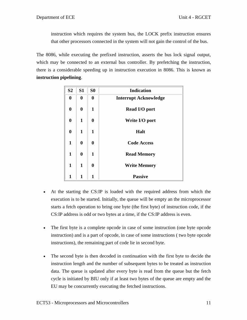
Department of ECE Unit 4 - RGCET
ECT53 - Microprocessors and Microcontrollers 11
instruction which requires the system bus the LOCK prefix instruction ensures
that other processors connected in the system will not gain the control of the bus
The 8086 while executing the prefixed instruction asserts the bus lock signal output
which may be connected to an external bus controller By prefetching the instruction
there is a considerable speeding up in instruction execution in 8086 This is known as
instruction pipelining
S2 S1 S0 Indication
0
0
0
0
1
1
1
1
0
0
1
1
0
0
1
1
0
1
0
1
0
1
0
1
Interrupt Acknowledge
Read IO port
Write IO port
Halt
Code Access
Read Memory
Write Memory
Passive
At the starting the CSIP is loaded with the required address from which the
execution is to be started Initially the queue will be empty an the microprocessor
starts a fetch operation to bring one byte (the first byte) of instruction code if the
CSIP address is odd or two bytes at a time if the CSIP address is even
The first byte is a complete opcode in case of some instruction (one byte opcode
instruction) and is a part of opcode in case of some instructions ( two byte opcode
instructions) the remaining part of code lie in second byte
The second byte is then decoded in continuation with the first byte to decide the
instruction length and the number of subsequent bytes to be treated as instruction
data The queue is updated after every byte is read from the queue but the fetch
cycle is initiated by BIU only if at least two bytes of the queue are empty and the
EU may be concurrently executing the fetched instructions
Department of ECE Unit 4 - RGCET
ECT53 - Microprocessors and Microcontrollers 12
The next byte after the instruction is completed is again the first opcode byte of
the next instruction A similar procedure is repeated till the complete execution of
the program The fetch operation of the next instruction is overlapped with the
execution of the current instruction As in the architecture there are two separate
units namely Execution unit and Bus interface unit
While the execution unit is busy in executing an instruction after it is completely
decoded the bus interface unit may be fetching the bytes of the next instruction
from memory depending upon the queue status
QS1 QS0 Indication
0
0
1
1
0
1
0
1
No Operation
First Byte of the opcode from the queue
Empty Queue
Subsequent Byte from the Queue
RQGT0 RQGT1 ndash RequestGrant These pins are used by the other local bus
master in maximum mode to force the processor to release the local bus at the
end of the processor current bus cycle
Each of the pin is bidirectional with RQGT0 having higher priority than
RQGT1 RQGT pins have internal pull-up resistors and may be left
unconnected RequestGrant sequence is as follows
1A pulse of one clock wide from another bus master requests the bus access to 8086
2During T4(current) or T1(next) clock cycle a pulse one clock wide from 8086 to the
requesting master indicates that the 8086 has allowed the local bus to float and that it
will enter the lsquohold acknowledgersquo state at next cycle The CPU bus interface unit is likely
to be disconnected from the local bus of the system
3A one clock wide pulse from the another master indicates to the 8086 that the hold
request is about to end and the 8086 may regain control of the local bus at the next clock
cycle Thus each master to master exchange of the local bus is a sequence of 3 pulses
There must be at least one dead clock cycle after each bus exchange The request and
grant pulses are active lowFor the bus request those are received while 8086 is
Department of ECE Unit 4 - RGCET
ECT53 - Microprocessors and Microcontrollers 13
performing memory or IO cycle the granting of the bus is governed by the rules as in
case of HOLD and HLDA in minimum mode
33 Maximum Mode 8086 System
In the maximum mode the 8086 is operated by strapping the MNMX pin to
ground
In this mode the processor derives the status signal S2 S1 S0 Another chip
called bus controller derives the control signal using this status information
In the maximum mode there may be more than one microprocessor in the system
configuration
The components in the system are same as in the minimum mode system
The basic function of the bus controller chip IC8288 is to derive control signals
like RD and WR ( for memory and IO devices) DEN DTR ALE etc using the
information by the processor on the status lines
The bus controller chip has input lines S2 S1 S0 and CLK These inputs to 8288
are driven by CPU
It derives the outputs ALE DEN DTR MRDC MWTC AMWC IORC IOWC
and AIOWC The AEN IOB and CEN pins are specially useful for
multiprocessor systems
Department of ECE Unit 4 - RGCET
ECT53 - Microprocessors and Microcontrollers 14
AEN and IOB are generally grounded CEN pin is usually tied to +5V The
significance of the MCEPDEN output depends upon the status of the IOB pin
If IOB is grounded it acts as master cascade enable to control cascade 8259A
else it acts as peripheral data enable used in the multiple bus configurations
INTA pin used to issue two interrupt acknowledge pulses to the interrupt
controller or to an interrupting device
IORC IOWC are IO read command and IO write command signals respectively
These signals enable an IO interface to read or write the data from or to the
address port
The MRDC MWTC are memory read command and memory write command
signals respectively and may be used as memory read or write signals
All these command signals instructs the memory to accept or send data from or to
the bus
For both of these write command signals the advanced signals namely AIOWC
and AMWTC are available
Department of ECE Unit 4 - RGCET
ECT53 - Microprocessors and Microcontrollers 15
Here the only difference between in timing diagram between minimum mode and
maximum mode is the status signals used and the available control and advanced
command signals
R0 S1 S2 are set at the beginning of bus cycle8288 bus controller will output a
pulse as on the ALE and apply a required signal to its DT R pin during T1
In T2 8288 will set DEN=1 thus enabling transceivers and for an input it will
activate MRDC or IORC These signals are activated until T4 For an output the
AMWC or AIOWC is activated from T2 to T4 and MWTC or IOWC is activated
from T3 to T4
The status bit S0 to S2 remains active until T3 and become passive during T3 and
T4
If reader input is not activated before T3 wait state will be inserted between T3
and T4
34 Minimum Mode 8086 System
In a minimum mode 8086 system the microprocessor 8086 is operated in
minimum mode by strapping its MNMX pin to logic 1
In this mode all the control signals are given out by the microprocessor chip
itselfThere is a single microprocessor in the minimum mode system
The remaining components in the system are latches transreceivers clock
generator memory and IO devices Some type of chip selection logic may be
required for selecting memory or IO devices depending upon the address map of
the system
Latches are generally buffered output D-type flip-flops like 74LS373 or 8282
They are used for separating the valid address from the multiplexed addressdata
signals and are controlled by the ALE signal generated by 8086
Transreceivers are the bidirectional buffers and some times they are called as data
amplifiers They are required to separate the valid data from the time multiplexed
addressdata signals
They are controlled by two signals namely DEN and DTR
Department of ECE Unit 4 - RGCET
ECT53 - Microprocessors and Microcontrollers 16
The DEN signal indicates the direction of data ie from or to the processor The
system contains memory for the monitor and users program storage
Usually EPROM are used for monitor storage while RAM for users program
storage A system may contain IO devices
RQGT Timings in Maximum Mode
The requestgrant response sequence contains a series of three pulses The
requestgrant pins are checked at each rising pulse of clock input
When a request is detected and if the condition for HOLD request is satisfied the
processor issues a grant pulse over the RQGT pin immediately during T4
(current) or T1 (next) state
When the requesting master receives this pulse it accepts the control of the bus it
sends a release pulse to the processor using RQGT pin
Maximum Mode Interface
When the 8086 is set for the maximum-mode configuration it provides signals for
implementing a multiprocessor coprocessor system environment
By multiprocessor environment we mean that one microprocessor exists in the
system and that each processor is executing its own program
Usually in this type of system environment there are some system resources that
are common to all processorsThey are called as global resources There are also
Department of ECE Unit 4 - RGCET
ECT53 - Microprocessors and Microcontrollers 17
other resources that are assigned to specific processors These are known as local
or private resources
Coprocessor also means that there is a second processor in the system In this two
processor does not access the bus at the same time One passes the control of the
system bus to the other and then may suspend its operation
In the maximum-mode 8086 system facilities are provided for implementing
allocation of global resources and passing bus control to other microprocessor or
coprocessor
8288 Bus Controller ndash Bus Command and Control Signals
8086 does not directly provide all the signals that are required to control the
memory IO and interrupt interfaces
Department of ECE Unit 4 - RGCET
ECT53 - Microprocessors and Microcontrollers 18
Specially the WR MIO DTR DEN ALE and INTA signals are no longer
produced by the 8086 Instead it outputs three status signals S0 S1 S2 prior to the
initiation of each bus cycle This 3- bit bus status code identifies which type of
bus cycle is to follow
S2S1S0 are input to the external bus controller device the bus controller
generates the appropriately timed command and control signals
S2 S1 S0 Indication 8288 Command
0
0
0
0
1
1
1
1
0
0
1
1
0
0
1
1
0
1
0
1
0
1
0
1
Interrupt Acknowledge
Read IO port
Write IO port
Halt
Instruction Fetch
Read Memory
Write Memory
Passive
INTA
IORC
IOWC AIOWC
None
MRDC
MRDC
MWTC AMWC
None
The 8288 produces one or two of these eight command signals for each bus
cycles For instance when the 8086 outputs the code S2S1S0 equals 001 it
indicates that an IO read cycle is to be performed
In the code 111 is output by the 8086 it is signaling that no bus activity is to take
place
The control outputs produced by the 8288 are DEN DTR and ALE These 3
signals provide the same functions as those described for the minimum system
mode This set of bus commands and control signals is compatible with the
Multibus and industry standard for interfacing microprocessor systems
The output of 8289 are bus arbitration signals
Bus busy (BUSY) common bus request (CBRQ) bus priority out (BPRO) bus
priority in (BPRN) bus request (BREQ) and bus clock (BCLK)
Department of ECE Unit 4 - RGCET
ECT53 - Microprocessors and Microcontrollers 19
They correspond to the bus exchange signals of the Multibus and are used to lock
other processor off the system bus during the execution of an instruction by the
8086
In this way the processor can be assured of uninterrupted access to common
system resources such as global memory
Queue Status Signals Two new signals that are produced by the 8086 in the
maximum-mode system are queue status outputs QS0 and QS1 Together they
form a 2-bit ueue status code QS1QS0
Following table shows the four different queue status
QS1 QS0 Queue Status
0 (low) 0 Queue Empty The queue has been reinitialized as a
result of the execution of a transfer instruction
0 1 First Byte The byte taken from the queue was the first
byte of the instruction
1 0 Queue Empty The queue has been reinitialized as a
result of the execution of a transfer instruction
1 1 Subsequent Byte The byte taken from the queue was a
subsequent byte of the instruction
Table - Queue status codes
Local Bus Control Signal ndash Request Grant Signals In a maximum mode
configuration the minimum mode HOLD HLDA interface is also changed
These two are replaced by requestgrant lines RQ GT0 and RQ GT1
respectively They provide a prioritized bus access mechanism for accessing the
local bus
Department of ECE Unit 4 - RGCET
ECT53 - Microprocessors and Microcontrollers 20
Memory Read Timing Diagram in Maximum Mode of 8086
Memory Write Timing in Maximum mode of 8086
Department of ECE Unit 4 - RGCET
ECT53 - Microprocessors and Microcontrollers 21
Minimum Mode Interface
When the Minimum mode operation is selected the 8086 provides all control
signals needed to implement the memory and IO interface
The minimum mode signal can be divided into the following basic groups
1 Addressdata bus
2 Status
3 Control
4 Interrupt and
5 DMA
Each and every group is explained clearly
AddressData Bus
These lines serve two functions As an address bus is 20 bits long and consists of
signal lines A0 through A19 A19 represents the MSB and A0 LSB A 20bit
address gives the 8086 a 1Mbyte memory address space More over it has an
independent IO address space which is 64K bytes in length
The 16 data bus lines D0 through D15 are actually multiplexed with address lines
A0 through A15 respectively By multiplexed we mean that the bus work as an
address bus during first machine cycle and as a data bus during next machine
cycles
D15 is the MSB and D0 LSB When acting as a data bus they carry readwrite
data for memory inputoutput data for IO devices and interrupt type codes from
an interrupt controller
Department of ECE Unit 4 - RGCET
ECT53 - Microprocessors and Microcontrollers 22
Status signal
The four most significant address lines A19 through A16 are also multiplexed but
in this case with status signals S6 through S3 These status bits are output on the
bus at the same time that data are transferred over the other bus lines
Bit S4 and S3 together from a 2 bit binary code that identifies which of the 8086
internal segment registers are used to generate the physical address that was
output on the address bus during the current bus cycleCode S4S3 = 00 identifies
a register known as extra segment register as the source of the segment address
Status line S5 reflects the status of another internal characteristic of the 8086 It is
the logic level of the internal enable flag The last status bit S6 is always at the
logic 0 level
S4 S3 Segment Register
0
0
0
1
Extra
Stack
Department of ECE Unit 4 - RGCET
ECT53 - Microprocessors and Microcontrollers 23
1
1
0
1
Code none
Data
Memory segment status codes
Control Signals
The control signals are provided to support the 8086 memory IO interfaces They
control functions such as when the bus is to carry a valid address in which
direction data are to be transferred over the bus when valid write data are on the
bus and when to put read data on the system bus
ALE is a pulse to logic 1 that signals external circuitry when a valid address word
is on the bus This address must be latched in external circuitry on the 1-to-0 edge
of the pulse at ALE
Another control signal that is produced during the bus cycle is BHE bank high
enable Logic 0 on this used as a memory enable signal for the most significant
byte half of the data bus D8 through D1 These lines also serves a second
function which is as the S7 status line
Using the MIO and DTR lines the 8086 signals which type of bus cycle is in
progress and in which direction data are to be transferred over the bus The logic
level of MIO tells external circuitry whether a memory or IO transfer is taking
place over the bus Logic 1 at this output signals a memory operation and logic 0
an IO operation
The direction of data transfer over the bus is signaled by the logic level output at
DTR When this line is logic 1 during the data transfer part of a bus cycle the
bus is in the transmit mode Therefore data are either written into memory or
output to an IO device On the other hand logic 0 at DTR signals that the bus is
in the receive mode This corresponds to reading data from memory or input of
data from an input port
Department of ECE Unit 4 - RGCET
ECT53 - Microprocessors and Microcontrollers 24
The signal read RD and write WR indicates that a read bus cycle or a write bus
cycle is in progress The 8086 switches WR to logic 0 to signal external device
that valid write or output data are on the bus
On the other hand RD indicates that the 8086 is performing a read of data of the
bus During read operations one other control signal is also supplied This is DEN
( data enable) and it signals external devices when they should put data on the
bus There is one other control signal that is involved with the memory and IO
interface This is the READY signal
READY signal is used to insert wait states into the bus cycle such that it is
extended by a number of clock periods This signal is provided by an external
clock generator device and can be supplied by the memory or IO sub-system to
signal the 8086 when they are ready to permit the data transfer to be completed
Interrupt signals
The key interrupt interface signals are interrupt request (INTR) and interrupt
acknowledge ( INTA)
INTR is an input to the 8086 that can be used by an external device to signal that
it need to be serviced
Logic 1 at INTR represents an active interrupt request When an interrupt request
has been recognized by the 8086 it indicates this fact to external circuit with
pulse to logic 0 at the INTA output
The TEST input is also related to the external interrupt interface Execution of a
WAIT instruction causes the 8086 to check the logic level at the TEST input
If the logic 1 is found the MPU suspend operation and goes into the idle state
The 8086 no longer executes instructions instead it repeatedly checks the logic
level of the TEST input waiting for its transition back to logic 0
As TEST switches to 0 execution resume with the next instruction in the
program This feature can be used to synchronize the operation of the 8086 to an
event in external hardware
There are two more inputs in the interrupt interface the nonmaskable interrupt
NMI and the reset interrupt RESET
Department of ECE Unit 4 - RGCET
ECT53 - Microprocessors and Microcontrollers 25
On the 0-to-1 transition of NMI control is passed to a nonmaskable interrupt
service routine The RESET input is used to provide a hardware reset for the
8086 Switching RESET to logic 0 initializes the internal register of the 8086 and
initiates a reset service routine
DMA Interface signals
The direct memory access DMA interface of the 8086 minimum mode consist of
the HOLD and HLDA signals
When an external device wants to take control of the system bus it signals to the
8086 by switching HOLD to the logic 1 level At the completion of the current
bus cycle the 8086 enters the hold state In the hold state signal lines AD0
through AD15 A16S3 through A19S6 BHE MIO DTR RD WR DEN and
INTR are all in the high Z state
The 8086 signals external device that it is in this state by switching its HLDA
output to logic 1 level
General Bus Operation
The 8086 has a combined address and data bus commonly referred as a time
multiplexed address and data bus
The main reason behind multiplexing address and data over the same pins is the
maximum utilisation of processor pins and it facilitates the use of 40 pin standard
DIP package
The bus can be demultiplexed using a few latches and transreceivers when ever
required
Basically all the processor bus cycles consist of at least four clock cycles These
are referred to as T1 T2 T3 T4 The address is transmitted by the processor
during T1 It is present on the bus only for one cycle
The negative edge of this ALE pulse is used to separate the address and the data
or status information In maximum mode the status lines S0 S1 and S2 are used
to indicate the type of operation
Status bits S3 to S7 are multiplexed with higher order address bits and the BHE
signal Address is valid during T1 while status bits S3 to S7 are valid during T2
through T4
Department of ECE Unit 4 - RGCET
ECT53 - Microprocessors and Microcontrollers 26
Maximum mode
In the maximum mode the 8086 is operated by strapping the MNMX pin to
ground
In this mode the processor derives the status signal S2 S1 S0 Another chip
called bus controller derives the control signal using this status information
In the maximum mode there may be more than one microprocessor in the system
configuration
Minimum mode
In a minimum mode 8086 system the microprocessor 8086 is operated in
minimum mode by strapping its MNMX pin to logic 1
In this mode all the control signals are given out by the microprocessor chip
itself
There is a single microprocessor in the minimum mode system
Bus Request and Bus Grant Timings in Minimum Mode System of 8086
Department of ECE Unit 4 - RGCET
ECT53 - Microprocessors and Microcontrollers 27
Hold Response sequence The HOLD pin is checked at leading edge of each clock
pulse If it is received active by the processor before T4 of the previous cycle or
during T1 state of the current cycle the CPU activates HLDA in the next clock
cycle and for succeeding bus cycles the bus will be given to another requesting
master
The control of the bus is not regained by the processor until the requesting master
does not drop the HOLD pin low When the request is dropped by the requesting
master the HLDA is dropped by the processor at the trailing edge of the next
clock
Write Cycle Timing Diagram for Minimum Mode
The working of the minimum mode configuration system can be better described
in terms of the timing diagrams rather than qualitatively describing the operations
The opcode fetch and read cycles are similar Hence the timing diagram can be
categorized in two parts the first is the timing diagram for read cycle and the
second is the timing diagram for write cycle
Department of ECE Unit 4 - RGCET
ECT53 - Microprocessors and Microcontrollers 28
The read cycle begins in T1 with the assertion of address latch enable (ALE)
signal and also M IO signal During the negative going edge of this signal the
valid address is latched on the local bus
The BHE and A0 signals address low high or both bytes From T1 to T4 the
MIO signal indicates a memory or IO operation
At T2 the address is removed from the local bus and is sent to the output The bus
is then tristated The read (RD) control signal is also activated in T2
The read (RD) signal causes the address device to enable its data bus drivers
After RD goes low the valid data is available on the data bus
The addressed device will drive the READY line high When the processor
returns the read signal to high level the addressed device will again tristate its bus
drivers
A write cycle also begins with the assertion of ALE and the emission of the
address The MIO signal is again asserted to indicate a memory or IO operation
Department of ECE Unit 4 - RGCET
ECT53 - Microprocessors and Microcontrollers 29
In T2 after sending the address in T1 the processor sends the data to be written to
the addressed location
The data remains on the bus until middle of T4 state The WR becomes active at
the beginning of T2 (unlike RD is somewhat delayed in T2 to provide time for
floating)
The BHE and A0 signals are used to select the proper byte or bytes of memory or
IO word to be read or write
The MIO RD and WR signals indicate the type of data transfer as specified in
table below
35 Addressing Modes of 8086
Definition An instruction acts on any number of operandsThe way an instruction
accesses its operands is called its Addressing modes
Operands may be of three types
o Implicit
o Explicit
o Both Implicit and Explicit
Implicit operands mean that the instruction by definition has some specific operands
The programmers do NOT select these operands
Example Implicit operands
XLAT automatically takes AL and BX as
operands
AAM it operates on the contents of AX
Explicit operands mean the instruction operates on the operands specified by the
programmer
Example Explicit operands
MOV AX BX it takes AX and BX as
Department of ECE Unit 4 - RGCET
ECT53 - Microprocessors and Microcontrollers 30
operands
XCHG SI DI it takes SI and DI as operands
Implicit and explicit operands
Example ImplicitExplicit operands
MUL BX automatically multiply BX explicitly times
AX
The location of an operand value in memory space is called the Effective Address (EA)
We can classify the addressing modes of 8086 into four groups
Immediate addressing
Register addressing
Memory addressing
IO port addressing
The first three Addresssing modes are clearly explained
Immediate addressing mode amp Register addressing mode
Immediate Addressing Mode
In this addressing mode the operand is stored as part of the instruction The immediate
operand which is stored along with the instruction resides in the code segment -- not in
the data segment This addressing mode is also faster to execute an instruction because
the operand is read with the instruction from memory Here are some examples
Example Immediate Operands
MOV AL 20 move the constant 20 into register AL
ADD AX 5 add constant 5 to register EAX
MOV DX offset msg move the address of message to
register DX
Register addressing mode
In this addressing mode the operands may be
Department of ECE Unit 4 - RGCET
ECT53 - Microprocessors and Microcontrollers 31
reg16 16-bit general registers AX BX CX DX SI DI SP or BP
reg8 8-bit general registers AH BH CH DH AL BL CL or DL
Sreg segment registers CS DS ES or SS There is an exception CS cannot be
a destination
For register addressing modes there is no need to compute the effective address The
operand is in a register and to get the operand there is no memory access involved
Example Register Operands
MOV AX BX mov reg16 reg16
ADD AX SI add reg16 reg16
MOV DS AX mov Sreg reg16
Some rules in register addressing modes
1 You may not specify CS as the destination operand
Example mov CS 02h ndashgt wrong
2 Only one of the operands can be a segment register You cannot move data from one
segment register to another with a single mov instruction To copy the value of cs to ds
you would have to use some sequence like
mov dscs -gt wrong
mov ax cs
mov ds ax -gt the way we do it
You should never use the segment registers as data registers to hold arbitrary values
They should only contain segment addresses
Memory Addressing Modes
Memory (RAM) is the main component of a computer to store temporary data and
machine instructions In a program programmers many times need to read from and
write into memory locations
There are different forms of memory addressing modes
Department of ECE Unit 4 - RGCET
ECT53 - Microprocessors and Microcontrollers 32
1 Direct Addressing
2 Register indirect addressing
3 Based addressing
4 Indexed addressing
5 Based indexed addressing
6 Based indexed with displacement
Direct Addressing Mode amp Register Indirect Addressing Mode
Direct Addressing Mode
The instruction mov alds[8088h] loads the AL register with a copy of the byte at
memory location 8088h Likewise the instruction mov ds[1234h]dl stores the value in
the dl register to memory location 1234h By default all displacement-only values
provide offsets into the data segment If you want to provide an offset into a different
segment you must use a segment override prefix before your address For example to
access location 1234h in the extra segment (es) you would use an instruction of the form
mov axes[1234h] Likewise to access this location in the code segment you would use
the instruction mov ax cs[1234h] The ds prefix in the previous examples is not a
segment override
Department of ECE Unit 4 - RGCET
ECT53 - Microprocessors and Microcontrollers 33
The instruction mov alds[8088h] is same as mov al [8088h] If not mentioned DS
register is taken by default
Register Indirect Addressing Mode
The 80x86 CPUs let you access memory indirectly through a register using the register
indirect addressing modes There are four forms of this addressing mode on the 8086
best demonstrated by the following instructions
mov al [bx]
mov al [bp]
mov al [si]
mov al [di]
Code Example
MOV BX 100H
MOV AL [BX]
The [bx] [si] and [di] modes use the ds segment by default The [bp] addressing mode
uses the stack segment (ss) by default You can use the segment override prefix symbols
if you wish to access data in different segments The following instructions demonstrate
the use of these overrides
mov al cs[bx]
mov al ds[bp]
mov al ss[si]
mov al es[di]
Intel refers to [bx] and [bp] as base addressing modes and bx and bp as base registers (in
fact bp stands for base pointer) Intel refers to the [si] and [di] addressing modes as
indexed addressing modes (si stands for source index di stands for destination index)
However these addressing modes are functionally equivalent This text will call these
forms register indirect modes to be consistent
Department of ECE Unit 4 - RGCET
ECT53 - Microprocessors and Microcontrollers 34
Based Addressing Mode and Indexed Addressing Modes
Based Addressing Mode
8-bit or 16-bit instruction operand is added to the contents of a base register (BX or BP)
the resulting value is a pointer to location where data resides
Mov al [bx][si]
Mov bl [bp][di]
Mov cl [bp][di]
Code Example
If bx=1000h
si=0880h
Mov AL [1000+880]
Mov AL[1880]
Indexed Addressing Modes
The indexed addressing modes use the following syntax
mov al [bx+disp]
mov al [bp+disp]
mov al [si+disp]
mov al [di+disp]
Code Example
MOV BX 100H
MOV AL [BX + 15]
MOV AL [BX + 16]
If bx contains 1000h then the instruction mov cl [bx+20h] will load cl from memory
location ds1020h Likewise if bp contains 2020h mov dh [bp+1000h] will load dh from
location ss3020 The offsets generated by these addressing modes are the sum of the
constant and the specified register The addressing modes involving bx si and di all use
Department of ECE Unit 4 - RGCET
ECT53 - Microprocessors and Microcontrollers 35
the data segment the [bp+disp] addressing mode uses the stack segment by default As
with the register indirect addressing modes you can use the segment override prefixes to
specify a different segment
mov al ss[bx+disp]
mov al es[bp+disp]
mov al cs[si+disp]
mov al ss[di+disp]
Based Indexed Addressing Modes amp Based Indexed Plus Displacement Addressing Mode
Based Indexed Addressing Modes
The based indexed addressing modes are simply combinations of the register indirect
addressing modes These addressing modes form the offset by adding together a base
register (bx or bp) and an index register (si or di) The allowable forms for these
addressing modes are
mov al [bx+si]
mov al [bx+di]
mov al [bp+si]
mov al [bp+di]
Code Example
MOV BX 100H
MOV SI 200H
MOV AL [BX + SI]
INC BX
INC SI
Department of ECE Unit 4 - RGCET
ECT53 - Microprocessors and Microcontrollers 36
Suppose that bx contains 1000h and si contains 880h Then the instruction mov al[bx][si]
would load al from location DS1880h Likewise if bp contains 1598h and di contains
1004 mov ax[bp+di] will load the 16 bits in ax from locations SS259C and SS259D
The addressing modes that do not involve bp use the data segment by default Those that
have bp as an operand use the stack segment by default
Based Indexed Plus Displacement Addressing Mode
These addressing modes are a slight modification of the baseindexed addressing modes
with the addition of an eight bit or sixteen bit constant The following are some examples
of these addressing modes
mov al disp[bx][si]
mov al disp[bx+di]
mov al [bp+si+disp]
mov al [bp][di][disp]
Department of ECE Unit 4 - RGCET
ECT53 - Microprocessors and Microcontrollers 37
Code Example
MOV BX 100H
MOV SI 200H
MOV AL [BX + SI +100H]
INC BX
INC SI
Index or Pointer Registers
These registers can also be called as Special Purpose registers
Department of ECE Unit 4 - RGCET
ECT53 - Microprocessors and Microcontrollers 38
Stack Pointer (SP) is a 16-bit register pointing to program stack ie it is used to hold the
address of the top of stack The stack is maintained as a LIFO with its bottom at the start
of the stack segment (specified by the SS segment register)Unlike the SP register the BP
can be used to specify the offset of other program segments
Base Pointer (BP) is a 16-bit register pointing to data in stack segment It is usually used
by subroutines to locate variables that were passed on the stack by a calling program BP
register is usually used for based based indexed or register indirect addressing
Source Index (SI) is a 16-bit register SI is used for indexed based indexed and register
indirect addressing as well as a source data address in string manipulation instructions
Used in conjunction with the DS register to point to data locations in the data segment
Destination Index (DI) is a 16-bit register Used in conjunction with the ES register in
string operations DI is used for indexed based indexed and register indirect addressing
as well as a destination data address in string manipulation instructions In short
Destination Index and SI Source Index registers are used to hold address
Segment Registers
Most of the registers contain datainstruction offsets within 64 KB memory segment
There are four different 64 KB segments for instructions stack data and extra data To
specify where in 1 MB of processor memory these 4 segments are located the processor
uses four segment registers
Department of ECE Unit 4 - RGCET
ECT53 - Microprocessors and Microcontrollers 39
Code segment (CS) is a 16-bit register containing address of 64 KB segment with
processor instructions The processor uses CS segment for all accesses to instructions
referenced by instruction pointer (IP) register CS register cannot be changed directly
The CS register is automatically updated during far jump far call and far return
instructions
Stack segment (SS) is a 16-bit register containing address of 64KB segment with
program stack By default the processor assumes that all data referenced by the stack
pointer (SP) and base pointer (BP) registers is located in the stack segment SS register
can be changed directly using POP instruction
Data segment (DS) is a 16-bit register containing address of 64KB segment with
program data By default the processor assumes that all data referenced by general
registers (AX BX CX DX) and index register (SI DI) is located in the data segment
DS register can be changed directly using POP and LDS instructions
Extra segment (ES) used to hold the starting address of Extra segment Extra segment is
provided for programs that need to access a second data segment Segment registers
cannot be used in arithmetic operations
Other registers of 8086
Instruction Pointer (IP) is a 16-bit register This is a crucially important register which
is used to control which instruction the CPU executes The ip or program counter is used
to store the memory location of the next instruction to be executed The CPU checks the
program counter to ascertain which instruction to carry out next It then updates the
program counter to point to the next instruction Thus the program counter will always
point to the next instruction to be executed
Flag Register contains a group of status bits called flags that indicate the status of the
CPU or the result of arithmetic operations There are two types of flags
Department of ECE Unit 4 - RGCET
ECT53 - Microprocessors and Microcontrollers 40
1 The status flags which reflect the result of executing an instruction The programmer
cannot setreset these flags directly
2 The control flags enable or disable certain CPU operations The programmer can
setreset these bits to control the CPUs operation
Nine individual bits of the status register are used as control flags (3 of them) and status
flags (6 of them)The remaining 7 are not used
A flag can only take on the values 0 and 1 We say a flag is set if it has the value 1The
status flags are used to record specific characteristics of arithmetic and of logical
instructions
Control Flags There are three control flags
1 The Direction Flag (D) Affects the direction of moving data blocks by such
instructions as MOVS CMPS and SCAS The flag values are 0 = up and 1 = down and
can be setreset by the STD (set D) and CLD (clear D) instructions
2 The Interrupt Flag (I) Dictates whether or not system interrupts can occur Interrupts
are actions initiated by hardware block such as input devices that will interrupt the
normal execution of programs The flag values are 0 = disable interrupts or 1 = enable
interrupts and can be manipulated by the CLI (clear I) and STI (set I) instructions
Department of ECE Unit 4 - RGCET
ECT53 - Microprocessors and Microcontrollers 41
3 The Trap Flag (T) Determines whether or not the CPU is halted after the execution
of each instruction When this flag is set (ie = 1) the programmer can single step
through his program to debug any errors When this flag = 0 this feature is off This flag
can be set by the INT 3 instruction
Status Flags There are six status flags
1 The Carry Flag (C) This flag is set when the result of an unsigned arithmetic
operation is too large to fit in the destination register This happens when there is an end
carry in an addition operation or there an end borrows in a subtraction operation A value
of 1 = carry and 0 = no carry
2 The Overflow Flag (O) This flag is set when the result of a signed arithmetic
operation is too large to fit in the destination register (ie when an overflow occurs)
Overflow can occur when adding two numbers with the same sign (ie both positive or
both negative) A value of 1 = overflow and 0 = no overflow
3 The Sign Flag (S) This flag is set when the result of an arithmetic or logic operation
is negative This flag is a copy of the MSB of the result (ie the sign bit) A value of 1
means negative and 0 = positive
4 The Zero Flag (Z) This flag is set when the result of an arithmetic or logic operation
is equal to zero A value of 1 means the result is zero and a value of 0 means the result is
not zero
5 The Auxiliary Carry Flag (A) This flag is set when an operation causes a carry from
bit 3 to bit 4 (or a borrow from bit 4 to bit 3) of an operand A value of 1 = carry and 0 =
no carry
6 The Parity Flag (P) This flags reflects the number of 1s in the result of an operation
If the number of 1s is even its value = 1 and if the number of 1s is odd then its value = 0
36 8086 Instruction Set and its Classification
The instructions of 8086 are classified into SIX groups They are
1 DATA TRANSFER INSTRUCTIONS
Department of ECE Unit 4 - RGCET
ECT53 - Microprocessors and Microcontrollers 42
2 ARITHMETIC INSTRUCTIONS
3 BIT MANIPULATION INSTRUCTIONS
4 STRING INSTRUCTIONS
5 PROGRAM EXECUTION TRANSFER INSTRUCTIONS
6 PROCESS CONTROL INSTRUCTIONS
1DATA TRANSFER INSTRUCTIONS
The DATA TRANSFER INSTRUCTIONS are those which transfers the DATA from
any one source to any one destinationThe datas may be of any type They are again
classified into four groupsThey are
GENERAL ndash PURPOSE
BYTE OR WORD
TRANSFER INSTRUCTIONS
SIMPLE INPUT AND
OUTPUT PORT
TRANSFER
INSTRUCTION
SPECIAL ADDRESS
TRANSFER
INSTRUCTION
FLAG
TRANSFER
INSTRUCTIONS
MOV
PUSH
POP
XCHG
XLAT
IN
OUT
LEA
LDS
LES
LAHF
SAHF
PUSHF
POPF
2ARITHMETIC INSTRUCTIONS
These instructions are those which are useful to perform Arithmetic calculations such as
addition subtraction multiplication and divisionThey are again classified into four
groupsThey are
ADDITION
INSTRUCTIONS
SUBTRACTION
INSTRUCTIONS
MULTIPLICATION
INSTRUCTIONS
DIVISION
INSTRUCTIONS
ADD
ADC
INC
AAA
DAA
SUB
SBB
DEC
NEG
CMP
AAS
DAS
MUL
IMUL
AAM
DIV
IDIV
AAD
CBW
CWD
3BIT MANIPULATION INSTRUCTIONS
Department of ECE Unit 4 - RGCET
ECT53 - Microprocessors and Microcontrollers 43
These instructions are used to perform Bit wise operations
LOGICAL INSTRUCTIONS SHIFT INSTRUCTIONS ROTATE INSTRUCTIONS
NOT
AND
OR
XOR
TEST
SHL SAL
SHR
SAR
ROL
ROR
RCL
RCR
4 STRING INSTRUCTIONS
The string instructions function easily on blocks of memoryThey are user friendly
instructions which help for easy program writing and execution They can speed up the
manipulating codeThey are useful in array handling tables and records
STRING INSTRUCTIONS
REP
REPE REPZ
REPNE REPNZ
MOVS MOVSB MOVSW
COMPS COMPSB
COMPSW
SCAS SCASB SCASW
LODS LODSB LODSW
STOS STOSB STOSW
5PROGRAM EXECUTION TRANSFER INSTRUCTIONS
These instructions transfer the program control from one address to other address ( Not
in a sequence) They are again classified into four groupsThey are
UNCONDITIONAL
TRANSFER
INSTRUCTIONS
CONDITIONAL
TRANSFER
INSTRUCTIONS
ITERATION CONTROL
INSTRUCTIONS
INTERRUPT
INSTRUCTIONS
CALL
RET
JMP
JA JNBE
JAE JNB
JB JNAE
JBE JNA
JC
JE JZ
JLE JNG
JNC
JNE JNZ
JNO
JNP JPO
JNS
LOOP
LOOPE LOOPZ
LOOPNE LOOPNZ
JCXZ
INT
INTO
IRET
Department of ECE Unit 4 - RGCET
ECT53 - Microprocessors and Microcontrollers 44
JG JNLE
JGE JNL
JL JNGE
JO
JP JPE
JS
6PROCESS CONTROL INSTRUCTIONS
These instructions are used to change the process of the Microprocessor They change the
process with the stored information They are again classified into Two groupsThey are
FLAG SET CLEAR
INSTRUCTIONS
EXTERNAL HARDWARE
SYNCHRONIZATION
INSTRUCTIONS
STC
CLC
CMC
STD
CLD
STI
CLI
HLT
WAIT
ESC
LOCK
NOP
37 Interrupts
Definition The meaning of lsquointerruptsrsquo is to break the sequence of operationWhile the
cpu is executing a programon lsquointerruptrsquo breaks the normal sequence of execution of
instructions diverts its execution to some other program called Interrupt Service Routine
(ISR)After executing ISR the control is transferred back again to the main
programInterrupt processing is an alternative to polling
Need for Interrupt Interrupts are particularly useful when interfacing IO devices that
provide or require data at relatively low data transfer rate
Types of Interrupts There are two types of Interrupts in 8086 They are
(i)Hardware Interrupts and
(ii)Software Interrupts
Department of ECE Unit 4 - RGCET
ECT53 - Microprocessors and Microcontrollers 45
(i) Hardware Interrupts (External Interrupts) The Intel microprocessors support
hardware interrupts through
Two pins that allow interrupt requests INTR and NMI
One pin that acknowledges INTA the interrupt requested on INTR
INTR and NMI
INTR is a maskable hardware interrupt The interrupt can be enableddisabled
using STICLI instructions or using more complicated method of updating the
FLAGS register with the help of the POPF instruction
When an interrupt occurs the processor stores FLAGS register into stack
disables further interrupts fetches from the bus one byte representing interrupt
type and jumps to interrupt processing routine address of which is stored in
location 4 ltinterrupt typegt Interrupt processing routine should return with the
IRET instruction
NMI is a non-maskable interrupt Interrupt is processed in the same way as the
INTR interrupt Interrupt type of the NMI is 2 ie the address of the NMI
processing routine is stored in location 0008h This interrupt has higher priority
than the maskable interrupt
ndash Ex NMI INTR
(ii) Software Interrupts (Internal Interrupts and Instructions) Software interrupts can
be caused by
INT instruction - breakpoint interrupt This is a type 3 interrupt
INT ltinterrupt numbergt instruction - any one interrupt from available 256
interrupts
INTO instruction - interrupt on overflow
Single-step interrupt - generated if the TF flag is set This is a type 1 interrupt
When the CPU processes this interrupt it clears TF flag before calling the
interrupt processing routine
Processor exceptions Divide Error (Type 0) Unused Opcode (type 6) and Escape
opcode (type 7)
Software interrupt processing is the same as for the hardware interrupts
Department of ECE Unit 4 - RGCET
ECT53 - Microprocessors and Microcontrollers 46
- Ex INT n (Software Instructions)
Control is provided through
o IF and TF flag bits
o IRET and IRETD
Performance of Hardware Interrupts
NMI Non maskable interrupts - TYPE 2 Interrupt
INTR Interrupt request - Between 20H and FFH
Interrupt Priority Structure
Performance of Software Interrupts
1 It decrements SP by 2 and pushes the flag register on the stack
2 Disables INTR by clearing the IF
3 It resets the TF in the flag Register
5 It decrements SP by 2 and pushes CS on the stack
Department of ECE Unit 4 - RGCET
ECT53 - Microprocessors and Microcontrollers 47
6 It decrements SP by 2 and pushes IP on the stack
6 Fetch the ISR address from the interrupt vector table
38 Other microprocessors the 80286 80386 and 80486 1048766 80286 Intel introduced 80286 in 1982
bull With 16-bit internal and external data bus
bull 24-bit address bus (224 = 16 megabyte)
bull virtual memory a way of fooling the microprocessor into thinking that it has access to
unlimited
memory by swapping data between disk storage and RAM
bull Real mode (faster operation with maximum of 1 Mbytes of memory) vs Protected
mode
protecting the operating system for accidental or deliberate destruction of the user
Protected
mode is slower but can use 16 Mbytes of memory
1048766 80386 introduced in 1985 also known as (80386DX)
bull With 32-bit internal and external data bus
bull 32-bit address bus (232 = 4 gigabyte-physical memory) With virtual memory 64
terabytes(246)
bull 80386SX was later introduced with the same internal structure with 16-bit external data
bus and
24-bit address bus 80386SX was much cheaper
1048766 All microprocessors discussed so far were general-purpose microprocessors and could
not handle
mathematical operations rapidly For this reason 8087 80287 80387 numeric data
processing chips
called math co-processors were used
1048766 80486 introduced in 1989 with 32-bit internal-external data bus and 32-bit address
bus
bull built in math co-processor in a single chip
bull Introduction of cache memory ( Static RAM with very fast access time)
Evolution of Intels Microprocessors
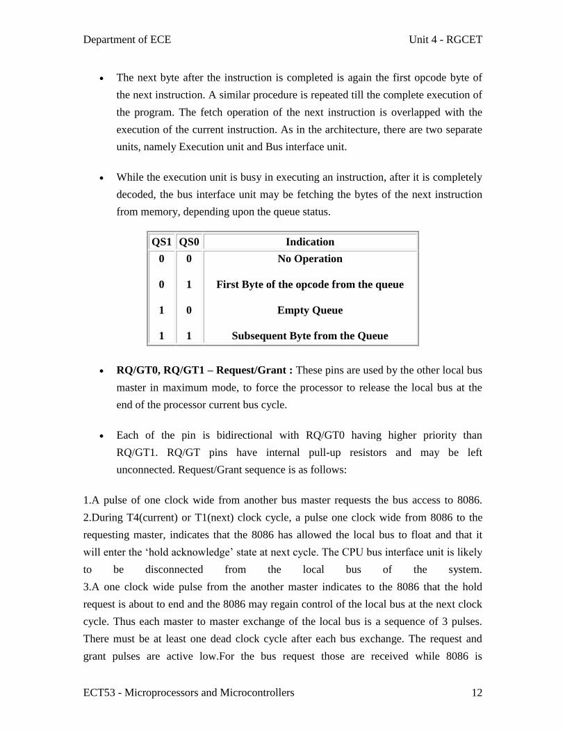
Department of ECE Unit 4 - RGCET
ECT53 - Microprocessors and Microcontrollers 12
The next byte after the instruction is completed is again the first opcode byte of
the next instruction A similar procedure is repeated till the complete execution of
the program The fetch operation of the next instruction is overlapped with the
execution of the current instruction As in the architecture there are two separate
units namely Execution unit and Bus interface unit
While the execution unit is busy in executing an instruction after it is completely
decoded the bus interface unit may be fetching the bytes of the next instruction
from memory depending upon the queue status
QS1 QS0 Indication
0
0
1
1
0
1
0
1
No Operation
First Byte of the opcode from the queue
Empty Queue
Subsequent Byte from the Queue
RQGT0 RQGT1 ndash RequestGrant These pins are used by the other local bus
master in maximum mode to force the processor to release the local bus at the
end of the processor current bus cycle
Each of the pin is bidirectional with RQGT0 having higher priority than
RQGT1 RQGT pins have internal pull-up resistors and may be left
unconnected RequestGrant sequence is as follows
1A pulse of one clock wide from another bus master requests the bus access to 8086
2During T4(current) or T1(next) clock cycle a pulse one clock wide from 8086 to the
requesting master indicates that the 8086 has allowed the local bus to float and that it
will enter the lsquohold acknowledgersquo state at next cycle The CPU bus interface unit is likely
to be disconnected from the local bus of the system
3A one clock wide pulse from the another master indicates to the 8086 that the hold
request is about to end and the 8086 may regain control of the local bus at the next clock
cycle Thus each master to master exchange of the local bus is a sequence of 3 pulses
There must be at least one dead clock cycle after each bus exchange The request and
grant pulses are active lowFor the bus request those are received while 8086 is
Department of ECE Unit 4 - RGCET
ECT53 - Microprocessors and Microcontrollers 13
performing memory or IO cycle the granting of the bus is governed by the rules as in
case of HOLD and HLDA in minimum mode
33 Maximum Mode 8086 System
In the maximum mode the 8086 is operated by strapping the MNMX pin to
ground
In this mode the processor derives the status signal S2 S1 S0 Another chip
called bus controller derives the control signal using this status information
In the maximum mode there may be more than one microprocessor in the system
configuration
The components in the system are same as in the minimum mode system
The basic function of the bus controller chip IC8288 is to derive control signals
like RD and WR ( for memory and IO devices) DEN DTR ALE etc using the
information by the processor on the status lines
The bus controller chip has input lines S2 S1 S0 and CLK These inputs to 8288
are driven by CPU
It derives the outputs ALE DEN DTR MRDC MWTC AMWC IORC IOWC
and AIOWC The AEN IOB and CEN pins are specially useful for
multiprocessor systems
Department of ECE Unit 4 - RGCET
ECT53 - Microprocessors and Microcontrollers 14
AEN and IOB are generally grounded CEN pin is usually tied to +5V The
significance of the MCEPDEN output depends upon the status of the IOB pin
If IOB is grounded it acts as master cascade enable to control cascade 8259A
else it acts as peripheral data enable used in the multiple bus configurations
INTA pin used to issue two interrupt acknowledge pulses to the interrupt
controller or to an interrupting device
IORC IOWC are IO read command and IO write command signals respectively
These signals enable an IO interface to read or write the data from or to the
address port
The MRDC MWTC are memory read command and memory write command
signals respectively and may be used as memory read or write signals
All these command signals instructs the memory to accept or send data from or to
the bus
For both of these write command signals the advanced signals namely AIOWC
and AMWTC are available
Department of ECE Unit 4 - RGCET
ECT53 - Microprocessors and Microcontrollers 15
Here the only difference between in timing diagram between minimum mode and
maximum mode is the status signals used and the available control and advanced
command signals
R0 S1 S2 are set at the beginning of bus cycle8288 bus controller will output a
pulse as on the ALE and apply a required signal to its DT R pin during T1
In T2 8288 will set DEN=1 thus enabling transceivers and for an input it will
activate MRDC or IORC These signals are activated until T4 For an output the
AMWC or AIOWC is activated from T2 to T4 and MWTC or IOWC is activated
from T3 to T4
The status bit S0 to S2 remains active until T3 and become passive during T3 and
T4
If reader input is not activated before T3 wait state will be inserted between T3
and T4
34 Minimum Mode 8086 System
In a minimum mode 8086 system the microprocessor 8086 is operated in
minimum mode by strapping its MNMX pin to logic 1
In this mode all the control signals are given out by the microprocessor chip
itselfThere is a single microprocessor in the minimum mode system
The remaining components in the system are latches transreceivers clock
generator memory and IO devices Some type of chip selection logic may be
required for selecting memory or IO devices depending upon the address map of
the system
Latches are generally buffered output D-type flip-flops like 74LS373 or 8282
They are used for separating the valid address from the multiplexed addressdata
signals and are controlled by the ALE signal generated by 8086
Transreceivers are the bidirectional buffers and some times they are called as data
amplifiers They are required to separate the valid data from the time multiplexed
addressdata signals
They are controlled by two signals namely DEN and DTR
Department of ECE Unit 4 - RGCET
ECT53 - Microprocessors and Microcontrollers 16
The DEN signal indicates the direction of data ie from or to the processor The
system contains memory for the monitor and users program storage
Usually EPROM are used for monitor storage while RAM for users program
storage A system may contain IO devices
RQGT Timings in Maximum Mode
The requestgrant response sequence contains a series of three pulses The
requestgrant pins are checked at each rising pulse of clock input
When a request is detected and if the condition for HOLD request is satisfied the
processor issues a grant pulse over the RQGT pin immediately during T4
(current) or T1 (next) state
When the requesting master receives this pulse it accepts the control of the bus it
sends a release pulse to the processor using RQGT pin
Maximum Mode Interface
When the 8086 is set for the maximum-mode configuration it provides signals for
implementing a multiprocessor coprocessor system environment
By multiprocessor environment we mean that one microprocessor exists in the
system and that each processor is executing its own program
Usually in this type of system environment there are some system resources that
are common to all processorsThey are called as global resources There are also
Department of ECE Unit 4 - RGCET
ECT53 - Microprocessors and Microcontrollers 17
other resources that are assigned to specific processors These are known as local
or private resources
Coprocessor also means that there is a second processor in the system In this two
processor does not access the bus at the same time One passes the control of the
system bus to the other and then may suspend its operation
In the maximum-mode 8086 system facilities are provided for implementing
allocation of global resources and passing bus control to other microprocessor or
coprocessor
8288 Bus Controller ndash Bus Command and Control Signals
8086 does not directly provide all the signals that are required to control the
memory IO and interrupt interfaces
Department of ECE Unit 4 - RGCET
ECT53 - Microprocessors and Microcontrollers 18
Specially the WR MIO DTR DEN ALE and INTA signals are no longer
produced by the 8086 Instead it outputs three status signals S0 S1 S2 prior to the
initiation of each bus cycle This 3- bit bus status code identifies which type of
bus cycle is to follow
S2S1S0 are input to the external bus controller device the bus controller
generates the appropriately timed command and control signals
S2 S1 S0 Indication 8288 Command
0
0
0
0
1
1
1
1
0
0
1
1
0
0
1
1
0
1
0
1
0
1
0
1
Interrupt Acknowledge
Read IO port
Write IO port
Halt
Instruction Fetch
Read Memory
Write Memory
Passive
INTA
IORC
IOWC AIOWC
None
MRDC
MRDC
MWTC AMWC
None
The 8288 produces one or two of these eight command signals for each bus
cycles For instance when the 8086 outputs the code S2S1S0 equals 001 it
indicates that an IO read cycle is to be performed
In the code 111 is output by the 8086 it is signaling that no bus activity is to take
place
The control outputs produced by the 8288 are DEN DTR and ALE These 3
signals provide the same functions as those described for the minimum system
mode This set of bus commands and control signals is compatible with the
Multibus and industry standard for interfacing microprocessor systems
The output of 8289 are bus arbitration signals
Bus busy (BUSY) common bus request (CBRQ) bus priority out (BPRO) bus
priority in (BPRN) bus request (BREQ) and bus clock (BCLK)
Department of ECE Unit 4 - RGCET
ECT53 - Microprocessors and Microcontrollers 19
They correspond to the bus exchange signals of the Multibus and are used to lock
other processor off the system bus during the execution of an instruction by the
8086
In this way the processor can be assured of uninterrupted access to common
system resources such as global memory
Queue Status Signals Two new signals that are produced by the 8086 in the
maximum-mode system are queue status outputs QS0 and QS1 Together they
form a 2-bit ueue status code QS1QS0
Following table shows the four different queue status
QS1 QS0 Queue Status
0 (low) 0 Queue Empty The queue has been reinitialized as a
result of the execution of a transfer instruction
0 1 First Byte The byte taken from the queue was the first
byte of the instruction
1 0 Queue Empty The queue has been reinitialized as a
result of the execution of a transfer instruction
1 1 Subsequent Byte The byte taken from the queue was a
subsequent byte of the instruction
Table - Queue status codes
Local Bus Control Signal ndash Request Grant Signals In a maximum mode
configuration the minimum mode HOLD HLDA interface is also changed
These two are replaced by requestgrant lines RQ GT0 and RQ GT1
respectively They provide a prioritized bus access mechanism for accessing the
local bus
Department of ECE Unit 4 - RGCET
ECT53 - Microprocessors and Microcontrollers 20
Memory Read Timing Diagram in Maximum Mode of 8086
Memory Write Timing in Maximum mode of 8086
Department of ECE Unit 4 - RGCET
ECT53 - Microprocessors and Microcontrollers 21
Minimum Mode Interface
When the Minimum mode operation is selected the 8086 provides all control
signals needed to implement the memory and IO interface
The minimum mode signal can be divided into the following basic groups
1 Addressdata bus
2 Status
3 Control
4 Interrupt and
5 DMA
Each and every group is explained clearly
AddressData Bus
These lines serve two functions As an address bus is 20 bits long and consists of
signal lines A0 through A19 A19 represents the MSB and A0 LSB A 20bit
address gives the 8086 a 1Mbyte memory address space More over it has an
independent IO address space which is 64K bytes in length
The 16 data bus lines D0 through D15 are actually multiplexed with address lines
A0 through A15 respectively By multiplexed we mean that the bus work as an
address bus during first machine cycle and as a data bus during next machine
cycles
D15 is the MSB and D0 LSB When acting as a data bus they carry readwrite
data for memory inputoutput data for IO devices and interrupt type codes from
an interrupt controller
Department of ECE Unit 4 - RGCET
ECT53 - Microprocessors and Microcontrollers 22
Status signal
The four most significant address lines A19 through A16 are also multiplexed but
in this case with status signals S6 through S3 These status bits are output on the
bus at the same time that data are transferred over the other bus lines
Bit S4 and S3 together from a 2 bit binary code that identifies which of the 8086
internal segment registers are used to generate the physical address that was
output on the address bus during the current bus cycleCode S4S3 = 00 identifies
a register known as extra segment register as the source of the segment address
Status line S5 reflects the status of another internal characteristic of the 8086 It is
the logic level of the internal enable flag The last status bit S6 is always at the
logic 0 level
S4 S3 Segment Register
0
0
0
1
Extra
Stack
Department of ECE Unit 4 - RGCET
ECT53 - Microprocessors and Microcontrollers 23
1
1
0
1
Code none
Data
Memory segment status codes
Control Signals
The control signals are provided to support the 8086 memory IO interfaces They
control functions such as when the bus is to carry a valid address in which
direction data are to be transferred over the bus when valid write data are on the
bus and when to put read data on the system bus
ALE is a pulse to logic 1 that signals external circuitry when a valid address word
is on the bus This address must be latched in external circuitry on the 1-to-0 edge
of the pulse at ALE
Another control signal that is produced during the bus cycle is BHE bank high
enable Logic 0 on this used as a memory enable signal for the most significant
byte half of the data bus D8 through D1 These lines also serves a second
function which is as the S7 status line
Using the MIO and DTR lines the 8086 signals which type of bus cycle is in
progress and in which direction data are to be transferred over the bus The logic
level of MIO tells external circuitry whether a memory or IO transfer is taking
place over the bus Logic 1 at this output signals a memory operation and logic 0
an IO operation
The direction of data transfer over the bus is signaled by the logic level output at
DTR When this line is logic 1 during the data transfer part of a bus cycle the
bus is in the transmit mode Therefore data are either written into memory or
output to an IO device On the other hand logic 0 at DTR signals that the bus is
in the receive mode This corresponds to reading data from memory or input of
data from an input port
Department of ECE Unit 4 - RGCET
ECT53 - Microprocessors and Microcontrollers 24
The signal read RD and write WR indicates that a read bus cycle or a write bus
cycle is in progress The 8086 switches WR to logic 0 to signal external device
that valid write or output data are on the bus
On the other hand RD indicates that the 8086 is performing a read of data of the
bus During read operations one other control signal is also supplied This is DEN
( data enable) and it signals external devices when they should put data on the
bus There is one other control signal that is involved with the memory and IO
interface This is the READY signal
READY signal is used to insert wait states into the bus cycle such that it is
extended by a number of clock periods This signal is provided by an external
clock generator device and can be supplied by the memory or IO sub-system to
signal the 8086 when they are ready to permit the data transfer to be completed
Interrupt signals
The key interrupt interface signals are interrupt request (INTR) and interrupt
acknowledge ( INTA)
INTR is an input to the 8086 that can be used by an external device to signal that
it need to be serviced
Logic 1 at INTR represents an active interrupt request When an interrupt request
has been recognized by the 8086 it indicates this fact to external circuit with
pulse to logic 0 at the INTA output
The TEST input is also related to the external interrupt interface Execution of a
WAIT instruction causes the 8086 to check the logic level at the TEST input
If the logic 1 is found the MPU suspend operation and goes into the idle state
The 8086 no longer executes instructions instead it repeatedly checks the logic
level of the TEST input waiting for its transition back to logic 0
As TEST switches to 0 execution resume with the next instruction in the
program This feature can be used to synchronize the operation of the 8086 to an
event in external hardware
There are two more inputs in the interrupt interface the nonmaskable interrupt
NMI and the reset interrupt RESET
Department of ECE Unit 4 - RGCET
ECT53 - Microprocessors and Microcontrollers 25
On the 0-to-1 transition of NMI control is passed to a nonmaskable interrupt
service routine The RESET input is used to provide a hardware reset for the
8086 Switching RESET to logic 0 initializes the internal register of the 8086 and
initiates a reset service routine
DMA Interface signals
The direct memory access DMA interface of the 8086 minimum mode consist of
the HOLD and HLDA signals
When an external device wants to take control of the system bus it signals to the
8086 by switching HOLD to the logic 1 level At the completion of the current
bus cycle the 8086 enters the hold state In the hold state signal lines AD0
through AD15 A16S3 through A19S6 BHE MIO DTR RD WR DEN and
INTR are all in the high Z state
The 8086 signals external device that it is in this state by switching its HLDA
output to logic 1 level
General Bus Operation
The 8086 has a combined address and data bus commonly referred as a time
multiplexed address and data bus
The main reason behind multiplexing address and data over the same pins is the
maximum utilisation of processor pins and it facilitates the use of 40 pin standard
DIP package
The bus can be demultiplexed using a few latches and transreceivers when ever
required
Basically all the processor bus cycles consist of at least four clock cycles These
are referred to as T1 T2 T3 T4 The address is transmitted by the processor
during T1 It is present on the bus only for one cycle
The negative edge of this ALE pulse is used to separate the address and the data
or status information In maximum mode the status lines S0 S1 and S2 are used
to indicate the type of operation
Status bits S3 to S7 are multiplexed with higher order address bits and the BHE
signal Address is valid during T1 while status bits S3 to S7 are valid during T2
through T4
Department of ECE Unit 4 - RGCET
ECT53 - Microprocessors and Microcontrollers 26
Maximum mode
In the maximum mode the 8086 is operated by strapping the MNMX pin to
ground
In this mode the processor derives the status signal S2 S1 S0 Another chip
called bus controller derives the control signal using this status information
In the maximum mode there may be more than one microprocessor in the system
configuration
Minimum mode
In a minimum mode 8086 system the microprocessor 8086 is operated in
minimum mode by strapping its MNMX pin to logic 1
In this mode all the control signals are given out by the microprocessor chip
itself
There is a single microprocessor in the minimum mode system
Bus Request and Bus Grant Timings in Minimum Mode System of 8086
Department of ECE Unit 4 - RGCET
ECT53 - Microprocessors and Microcontrollers 27
Hold Response sequence The HOLD pin is checked at leading edge of each clock
pulse If it is received active by the processor before T4 of the previous cycle or
during T1 state of the current cycle the CPU activates HLDA in the next clock
cycle and for succeeding bus cycles the bus will be given to another requesting
master
The control of the bus is not regained by the processor until the requesting master
does not drop the HOLD pin low When the request is dropped by the requesting
master the HLDA is dropped by the processor at the trailing edge of the next
clock
Write Cycle Timing Diagram for Minimum Mode
The working of the minimum mode configuration system can be better described
in terms of the timing diagrams rather than qualitatively describing the operations
The opcode fetch and read cycles are similar Hence the timing diagram can be
categorized in two parts the first is the timing diagram for read cycle and the
second is the timing diagram for write cycle
Department of ECE Unit 4 - RGCET
ECT53 - Microprocessors and Microcontrollers 28
The read cycle begins in T1 with the assertion of address latch enable (ALE)
signal and also M IO signal During the negative going edge of this signal the
valid address is latched on the local bus
The BHE and A0 signals address low high or both bytes From T1 to T4 the
MIO signal indicates a memory or IO operation
At T2 the address is removed from the local bus and is sent to the output The bus
is then tristated The read (RD) control signal is also activated in T2
The read (RD) signal causes the address device to enable its data bus drivers
After RD goes low the valid data is available on the data bus
The addressed device will drive the READY line high When the processor
returns the read signal to high level the addressed device will again tristate its bus
drivers
A write cycle also begins with the assertion of ALE and the emission of the
address The MIO signal is again asserted to indicate a memory or IO operation
Department of ECE Unit 4 - RGCET
ECT53 - Microprocessors and Microcontrollers 29
In T2 after sending the address in T1 the processor sends the data to be written to
the addressed location
The data remains on the bus until middle of T4 state The WR becomes active at
the beginning of T2 (unlike RD is somewhat delayed in T2 to provide time for
floating)
The BHE and A0 signals are used to select the proper byte or bytes of memory or
IO word to be read or write
The MIO RD and WR signals indicate the type of data transfer as specified in
table below
35 Addressing Modes of 8086
Definition An instruction acts on any number of operandsThe way an instruction
accesses its operands is called its Addressing modes
Operands may be of three types
o Implicit
o Explicit
o Both Implicit and Explicit
Implicit operands mean that the instruction by definition has some specific operands
The programmers do NOT select these operands
Example Implicit operands
XLAT automatically takes AL and BX as
operands
AAM it operates on the contents of AX
Explicit operands mean the instruction operates on the operands specified by the
programmer
Example Explicit operands
MOV AX BX it takes AX and BX as
Department of ECE Unit 4 - RGCET
ECT53 - Microprocessors and Microcontrollers 30
operands
XCHG SI DI it takes SI and DI as operands
Implicit and explicit operands
Example ImplicitExplicit operands
MUL BX automatically multiply BX explicitly times
AX
The location of an operand value in memory space is called the Effective Address (EA)
We can classify the addressing modes of 8086 into four groups
Immediate addressing
Register addressing
Memory addressing
IO port addressing
The first three Addresssing modes are clearly explained
Immediate addressing mode amp Register addressing mode
Immediate Addressing Mode
In this addressing mode the operand is stored as part of the instruction The immediate
operand which is stored along with the instruction resides in the code segment -- not in
the data segment This addressing mode is also faster to execute an instruction because
the operand is read with the instruction from memory Here are some examples
Example Immediate Operands
MOV AL 20 move the constant 20 into register AL
ADD AX 5 add constant 5 to register EAX
MOV DX offset msg move the address of message to
register DX
Register addressing mode
In this addressing mode the operands may be
Department of ECE Unit 4 - RGCET
ECT53 - Microprocessors and Microcontrollers 31
reg16 16-bit general registers AX BX CX DX SI DI SP or BP
reg8 8-bit general registers AH BH CH DH AL BL CL or DL
Sreg segment registers CS DS ES or SS There is an exception CS cannot be
a destination
For register addressing modes there is no need to compute the effective address The
operand is in a register and to get the operand there is no memory access involved
Example Register Operands
MOV AX BX mov reg16 reg16
ADD AX SI add reg16 reg16
MOV DS AX mov Sreg reg16
Some rules in register addressing modes
1 You may not specify CS as the destination operand
Example mov CS 02h ndashgt wrong
2 Only one of the operands can be a segment register You cannot move data from one
segment register to another with a single mov instruction To copy the value of cs to ds
you would have to use some sequence like
mov dscs -gt wrong
mov ax cs
mov ds ax -gt the way we do it
You should never use the segment registers as data registers to hold arbitrary values
They should only contain segment addresses
Memory Addressing Modes
Memory (RAM) is the main component of a computer to store temporary data and
machine instructions In a program programmers many times need to read from and
write into memory locations
There are different forms of memory addressing modes
Department of ECE Unit 4 - RGCET
ECT53 - Microprocessors and Microcontrollers 32
1 Direct Addressing
2 Register indirect addressing
3 Based addressing
4 Indexed addressing
5 Based indexed addressing
6 Based indexed with displacement
Direct Addressing Mode amp Register Indirect Addressing Mode
Direct Addressing Mode
The instruction mov alds[8088h] loads the AL register with a copy of the byte at
memory location 8088h Likewise the instruction mov ds[1234h]dl stores the value in
the dl register to memory location 1234h By default all displacement-only values
provide offsets into the data segment If you want to provide an offset into a different
segment you must use a segment override prefix before your address For example to
access location 1234h in the extra segment (es) you would use an instruction of the form
mov axes[1234h] Likewise to access this location in the code segment you would use
the instruction mov ax cs[1234h] The ds prefix in the previous examples is not a
segment override
Department of ECE Unit 4 - RGCET
ECT53 - Microprocessors and Microcontrollers 33
The instruction mov alds[8088h] is same as mov al [8088h] If not mentioned DS
register is taken by default
Register Indirect Addressing Mode
The 80x86 CPUs let you access memory indirectly through a register using the register
indirect addressing modes There are four forms of this addressing mode on the 8086
best demonstrated by the following instructions
mov al [bx]
mov al [bp]
mov al [si]
mov al [di]
Code Example
MOV BX 100H
MOV AL [BX]
The [bx] [si] and [di] modes use the ds segment by default The [bp] addressing mode
uses the stack segment (ss) by default You can use the segment override prefix symbols
if you wish to access data in different segments The following instructions demonstrate
the use of these overrides
mov al cs[bx]
mov al ds[bp]
mov al ss[si]
mov al es[di]
Intel refers to [bx] and [bp] as base addressing modes and bx and bp as base registers (in
fact bp stands for base pointer) Intel refers to the [si] and [di] addressing modes as
indexed addressing modes (si stands for source index di stands for destination index)
However these addressing modes are functionally equivalent This text will call these
forms register indirect modes to be consistent
Department of ECE Unit 4 - RGCET
ECT53 - Microprocessors and Microcontrollers 34
Based Addressing Mode and Indexed Addressing Modes
Based Addressing Mode
8-bit or 16-bit instruction operand is added to the contents of a base register (BX or BP)
the resulting value is a pointer to location where data resides
Mov al [bx][si]
Mov bl [bp][di]
Mov cl [bp][di]
Code Example
If bx=1000h
si=0880h
Mov AL [1000+880]
Mov AL[1880]
Indexed Addressing Modes
The indexed addressing modes use the following syntax
mov al [bx+disp]
mov al [bp+disp]
mov al [si+disp]
mov al [di+disp]
Code Example
MOV BX 100H
MOV AL [BX + 15]
MOV AL [BX + 16]
If bx contains 1000h then the instruction mov cl [bx+20h] will load cl from memory
location ds1020h Likewise if bp contains 2020h mov dh [bp+1000h] will load dh from
location ss3020 The offsets generated by these addressing modes are the sum of the
constant and the specified register The addressing modes involving bx si and di all use
Department of ECE Unit 4 - RGCET
ECT53 - Microprocessors and Microcontrollers 35
the data segment the [bp+disp] addressing mode uses the stack segment by default As
with the register indirect addressing modes you can use the segment override prefixes to
specify a different segment
mov al ss[bx+disp]
mov al es[bp+disp]
mov al cs[si+disp]
mov al ss[di+disp]
Based Indexed Addressing Modes amp Based Indexed Plus Displacement Addressing Mode
Based Indexed Addressing Modes
The based indexed addressing modes are simply combinations of the register indirect
addressing modes These addressing modes form the offset by adding together a base
register (bx or bp) and an index register (si or di) The allowable forms for these
addressing modes are
mov al [bx+si]
mov al [bx+di]
mov al [bp+si]
mov al [bp+di]
Code Example
MOV BX 100H
MOV SI 200H
MOV AL [BX + SI]
INC BX
INC SI
Department of ECE Unit 4 - RGCET
ECT53 - Microprocessors and Microcontrollers 36
Suppose that bx contains 1000h and si contains 880h Then the instruction mov al[bx][si]
would load al from location DS1880h Likewise if bp contains 1598h and di contains
1004 mov ax[bp+di] will load the 16 bits in ax from locations SS259C and SS259D
The addressing modes that do not involve bp use the data segment by default Those that
have bp as an operand use the stack segment by default
Based Indexed Plus Displacement Addressing Mode
These addressing modes are a slight modification of the baseindexed addressing modes
with the addition of an eight bit or sixteen bit constant The following are some examples
of these addressing modes
mov al disp[bx][si]
mov al disp[bx+di]
mov al [bp+si+disp]
mov al [bp][di][disp]
Department of ECE Unit 4 - RGCET
ECT53 - Microprocessors and Microcontrollers 37
Code Example
MOV BX 100H
MOV SI 200H
MOV AL [BX + SI +100H]
INC BX
INC SI
Index or Pointer Registers
These registers can also be called as Special Purpose registers
Department of ECE Unit 4 - RGCET
ECT53 - Microprocessors and Microcontrollers 38
Stack Pointer (SP) is a 16-bit register pointing to program stack ie it is used to hold the
address of the top of stack The stack is maintained as a LIFO with its bottom at the start
of the stack segment (specified by the SS segment register)Unlike the SP register the BP
can be used to specify the offset of other program segments
Base Pointer (BP) is a 16-bit register pointing to data in stack segment It is usually used
by subroutines to locate variables that were passed on the stack by a calling program BP
register is usually used for based based indexed or register indirect addressing
Source Index (SI) is a 16-bit register SI is used for indexed based indexed and register
indirect addressing as well as a source data address in string manipulation instructions
Used in conjunction with the DS register to point to data locations in the data segment
Destination Index (DI) is a 16-bit register Used in conjunction with the ES register in
string operations DI is used for indexed based indexed and register indirect addressing
as well as a destination data address in string manipulation instructions In short
Destination Index and SI Source Index registers are used to hold address
Segment Registers
Most of the registers contain datainstruction offsets within 64 KB memory segment
There are four different 64 KB segments for instructions stack data and extra data To
specify where in 1 MB of processor memory these 4 segments are located the processor
uses four segment registers
Department of ECE Unit 4 - RGCET
ECT53 - Microprocessors and Microcontrollers 39
Code segment (CS) is a 16-bit register containing address of 64 KB segment with
processor instructions The processor uses CS segment for all accesses to instructions
referenced by instruction pointer (IP) register CS register cannot be changed directly
The CS register is automatically updated during far jump far call and far return
instructions
Stack segment (SS) is a 16-bit register containing address of 64KB segment with
program stack By default the processor assumes that all data referenced by the stack
pointer (SP) and base pointer (BP) registers is located in the stack segment SS register
can be changed directly using POP instruction
Data segment (DS) is a 16-bit register containing address of 64KB segment with
program data By default the processor assumes that all data referenced by general
registers (AX BX CX DX) and index register (SI DI) is located in the data segment
DS register can be changed directly using POP and LDS instructions
Extra segment (ES) used to hold the starting address of Extra segment Extra segment is
provided for programs that need to access a second data segment Segment registers
cannot be used in arithmetic operations
Other registers of 8086
Instruction Pointer (IP) is a 16-bit register This is a crucially important register which
is used to control which instruction the CPU executes The ip or program counter is used
to store the memory location of the next instruction to be executed The CPU checks the
program counter to ascertain which instruction to carry out next It then updates the
program counter to point to the next instruction Thus the program counter will always
point to the next instruction to be executed
Flag Register contains a group of status bits called flags that indicate the status of the
CPU or the result of arithmetic operations There are two types of flags
Department of ECE Unit 4 - RGCET
ECT53 - Microprocessors and Microcontrollers 40
1 The status flags which reflect the result of executing an instruction The programmer
cannot setreset these flags directly
2 The control flags enable or disable certain CPU operations The programmer can
setreset these bits to control the CPUs operation
Nine individual bits of the status register are used as control flags (3 of them) and status
flags (6 of them)The remaining 7 are not used
A flag can only take on the values 0 and 1 We say a flag is set if it has the value 1The
status flags are used to record specific characteristics of arithmetic and of logical
instructions
Control Flags There are three control flags
1 The Direction Flag (D) Affects the direction of moving data blocks by such
instructions as MOVS CMPS and SCAS The flag values are 0 = up and 1 = down and
can be setreset by the STD (set D) and CLD (clear D) instructions
2 The Interrupt Flag (I) Dictates whether or not system interrupts can occur Interrupts
are actions initiated by hardware block such as input devices that will interrupt the
normal execution of programs The flag values are 0 = disable interrupts or 1 = enable
interrupts and can be manipulated by the CLI (clear I) and STI (set I) instructions
Department of ECE Unit 4 - RGCET
ECT53 - Microprocessors and Microcontrollers 41
3 The Trap Flag (T) Determines whether or not the CPU is halted after the execution
of each instruction When this flag is set (ie = 1) the programmer can single step
through his program to debug any errors When this flag = 0 this feature is off This flag
can be set by the INT 3 instruction
Status Flags There are six status flags
1 The Carry Flag (C) This flag is set when the result of an unsigned arithmetic
operation is too large to fit in the destination register This happens when there is an end
carry in an addition operation or there an end borrows in a subtraction operation A value
of 1 = carry and 0 = no carry
2 The Overflow Flag (O) This flag is set when the result of a signed arithmetic
operation is too large to fit in the destination register (ie when an overflow occurs)
Overflow can occur when adding two numbers with the same sign (ie both positive or
both negative) A value of 1 = overflow and 0 = no overflow
3 The Sign Flag (S) This flag is set when the result of an arithmetic or logic operation
is negative This flag is a copy of the MSB of the result (ie the sign bit) A value of 1
means negative and 0 = positive
4 The Zero Flag (Z) This flag is set when the result of an arithmetic or logic operation
is equal to zero A value of 1 means the result is zero and a value of 0 means the result is
not zero
5 The Auxiliary Carry Flag (A) This flag is set when an operation causes a carry from
bit 3 to bit 4 (or a borrow from bit 4 to bit 3) of an operand A value of 1 = carry and 0 =
no carry
6 The Parity Flag (P) This flags reflects the number of 1s in the result of an operation
If the number of 1s is even its value = 1 and if the number of 1s is odd then its value = 0
36 8086 Instruction Set and its Classification
The instructions of 8086 are classified into SIX groups They are
1 DATA TRANSFER INSTRUCTIONS
Department of ECE Unit 4 - RGCET
ECT53 - Microprocessors and Microcontrollers 42
2 ARITHMETIC INSTRUCTIONS
3 BIT MANIPULATION INSTRUCTIONS
4 STRING INSTRUCTIONS
5 PROGRAM EXECUTION TRANSFER INSTRUCTIONS
6 PROCESS CONTROL INSTRUCTIONS
1DATA TRANSFER INSTRUCTIONS
The DATA TRANSFER INSTRUCTIONS are those which transfers the DATA from
any one source to any one destinationThe datas may be of any type They are again
classified into four groupsThey are
GENERAL ndash PURPOSE
BYTE OR WORD
TRANSFER INSTRUCTIONS
SIMPLE INPUT AND
OUTPUT PORT
TRANSFER
INSTRUCTION
SPECIAL ADDRESS
TRANSFER
INSTRUCTION
FLAG
TRANSFER
INSTRUCTIONS
MOV
PUSH
POP
XCHG
XLAT
IN
OUT
LEA
LDS
LES
LAHF
SAHF
PUSHF
POPF
2ARITHMETIC INSTRUCTIONS
These instructions are those which are useful to perform Arithmetic calculations such as
addition subtraction multiplication and divisionThey are again classified into four
groupsThey are
ADDITION
INSTRUCTIONS
SUBTRACTION
INSTRUCTIONS
MULTIPLICATION
INSTRUCTIONS
DIVISION
INSTRUCTIONS
ADD
ADC
INC
AAA
DAA
SUB
SBB
DEC
NEG
CMP
AAS
DAS
MUL
IMUL
AAM
DIV
IDIV
AAD
CBW
CWD
3BIT MANIPULATION INSTRUCTIONS
Department of ECE Unit 4 - RGCET
ECT53 - Microprocessors and Microcontrollers 43
These instructions are used to perform Bit wise operations
LOGICAL INSTRUCTIONS SHIFT INSTRUCTIONS ROTATE INSTRUCTIONS
NOT
AND
OR
XOR
TEST
SHL SAL
SHR
SAR
ROL
ROR
RCL
RCR
4 STRING INSTRUCTIONS
The string instructions function easily on blocks of memoryThey are user friendly
instructions which help for easy program writing and execution They can speed up the
manipulating codeThey are useful in array handling tables and records
STRING INSTRUCTIONS
REP
REPE REPZ
REPNE REPNZ
MOVS MOVSB MOVSW
COMPS COMPSB
COMPSW
SCAS SCASB SCASW
LODS LODSB LODSW
STOS STOSB STOSW
5PROGRAM EXECUTION TRANSFER INSTRUCTIONS
These instructions transfer the program control from one address to other address ( Not
in a sequence) They are again classified into four groupsThey are
UNCONDITIONAL
TRANSFER
INSTRUCTIONS
CONDITIONAL
TRANSFER
INSTRUCTIONS
ITERATION CONTROL
INSTRUCTIONS
INTERRUPT
INSTRUCTIONS
CALL
RET
JMP
JA JNBE
JAE JNB
JB JNAE
JBE JNA
JC
JE JZ
JLE JNG
JNC
JNE JNZ
JNO
JNP JPO
JNS
LOOP
LOOPE LOOPZ
LOOPNE LOOPNZ
JCXZ
INT
INTO
IRET
Department of ECE Unit 4 - RGCET
ECT53 - Microprocessors and Microcontrollers 44
JG JNLE
JGE JNL
JL JNGE
JO
JP JPE
JS
6PROCESS CONTROL INSTRUCTIONS
These instructions are used to change the process of the Microprocessor They change the
process with the stored information They are again classified into Two groupsThey are
FLAG SET CLEAR
INSTRUCTIONS
EXTERNAL HARDWARE
SYNCHRONIZATION
INSTRUCTIONS
STC
CLC
CMC
STD
CLD
STI
CLI
HLT
WAIT
ESC
LOCK
NOP
37 Interrupts
Definition The meaning of lsquointerruptsrsquo is to break the sequence of operationWhile the
cpu is executing a programon lsquointerruptrsquo breaks the normal sequence of execution of
instructions diverts its execution to some other program called Interrupt Service Routine
(ISR)After executing ISR the control is transferred back again to the main
programInterrupt processing is an alternative to polling
Need for Interrupt Interrupts are particularly useful when interfacing IO devices that
provide or require data at relatively low data transfer rate
Types of Interrupts There are two types of Interrupts in 8086 They are
(i)Hardware Interrupts and
(ii)Software Interrupts
Department of ECE Unit 4 - RGCET
ECT53 - Microprocessors and Microcontrollers 45
(i) Hardware Interrupts (External Interrupts) The Intel microprocessors support
hardware interrupts through
Two pins that allow interrupt requests INTR and NMI
One pin that acknowledges INTA the interrupt requested on INTR
INTR and NMI
INTR is a maskable hardware interrupt The interrupt can be enableddisabled
using STICLI instructions or using more complicated method of updating the
FLAGS register with the help of the POPF instruction
When an interrupt occurs the processor stores FLAGS register into stack
disables further interrupts fetches from the bus one byte representing interrupt
type and jumps to interrupt processing routine address of which is stored in
location 4 ltinterrupt typegt Interrupt processing routine should return with the
IRET instruction
NMI is a non-maskable interrupt Interrupt is processed in the same way as the
INTR interrupt Interrupt type of the NMI is 2 ie the address of the NMI
processing routine is stored in location 0008h This interrupt has higher priority
than the maskable interrupt
ndash Ex NMI INTR
(ii) Software Interrupts (Internal Interrupts and Instructions) Software interrupts can
be caused by
INT instruction - breakpoint interrupt This is a type 3 interrupt
INT ltinterrupt numbergt instruction - any one interrupt from available 256
interrupts
INTO instruction - interrupt on overflow
Single-step interrupt - generated if the TF flag is set This is a type 1 interrupt
When the CPU processes this interrupt it clears TF flag before calling the
interrupt processing routine
Processor exceptions Divide Error (Type 0) Unused Opcode (type 6) and Escape
opcode (type 7)
Software interrupt processing is the same as for the hardware interrupts
Department of ECE Unit 4 - RGCET
ECT53 - Microprocessors and Microcontrollers 46
- Ex INT n (Software Instructions)
Control is provided through
o IF and TF flag bits
o IRET and IRETD
Performance of Hardware Interrupts
NMI Non maskable interrupts - TYPE 2 Interrupt
INTR Interrupt request - Between 20H and FFH
Interrupt Priority Structure
Performance of Software Interrupts
1 It decrements SP by 2 and pushes the flag register on the stack
2 Disables INTR by clearing the IF
3 It resets the TF in the flag Register
5 It decrements SP by 2 and pushes CS on the stack
Department of ECE Unit 4 - RGCET
ECT53 - Microprocessors and Microcontrollers 47
6 It decrements SP by 2 and pushes IP on the stack
6 Fetch the ISR address from the interrupt vector table
38 Other microprocessors the 80286 80386 and 80486 1048766 80286 Intel introduced 80286 in 1982
bull With 16-bit internal and external data bus
bull 24-bit address bus (224 = 16 megabyte)
bull virtual memory a way of fooling the microprocessor into thinking that it has access to
unlimited
memory by swapping data between disk storage and RAM
bull Real mode (faster operation with maximum of 1 Mbytes of memory) vs Protected
mode
protecting the operating system for accidental or deliberate destruction of the user
Protected
mode is slower but can use 16 Mbytes of memory
1048766 80386 introduced in 1985 also known as (80386DX)
bull With 32-bit internal and external data bus
bull 32-bit address bus (232 = 4 gigabyte-physical memory) With virtual memory 64
terabytes(246)
bull 80386SX was later introduced with the same internal structure with 16-bit external data
bus and
24-bit address bus 80386SX was much cheaper
1048766 All microprocessors discussed so far were general-purpose microprocessors and could
not handle
mathematical operations rapidly For this reason 8087 80287 80387 numeric data
processing chips
called math co-processors were used
1048766 80486 introduced in 1989 with 32-bit internal-external data bus and 32-bit address
bus
bull built in math co-processor in a single chip
bull Introduction of cache memory ( Static RAM with very fast access time)
Evolution of Intels Microprocessors
Department of ECE Unit 4 - RGCET
ECT53 - Microprocessors and Microcontrollers 13
performing memory or IO cycle the granting of the bus is governed by the rules as in
case of HOLD and HLDA in minimum mode
33 Maximum Mode 8086 System
In the maximum mode the 8086 is operated by strapping the MNMX pin to
ground
In this mode the processor derives the status signal S2 S1 S0 Another chip
called bus controller derives the control signal using this status information
In the maximum mode there may be more than one microprocessor in the system
configuration
The components in the system are same as in the minimum mode system
The basic function of the bus controller chip IC8288 is to derive control signals
like RD and WR ( for memory and IO devices) DEN DTR ALE etc using the
information by the processor on the status lines
The bus controller chip has input lines S2 S1 S0 and CLK These inputs to 8288
are driven by CPU
It derives the outputs ALE DEN DTR MRDC MWTC AMWC IORC IOWC
and AIOWC The AEN IOB and CEN pins are specially useful for
multiprocessor systems
Department of ECE Unit 4 - RGCET
ECT53 - Microprocessors and Microcontrollers 14
AEN and IOB are generally grounded CEN pin is usually tied to +5V The
significance of the MCEPDEN output depends upon the status of the IOB pin
If IOB is grounded it acts as master cascade enable to control cascade 8259A
else it acts as peripheral data enable used in the multiple bus configurations
INTA pin used to issue two interrupt acknowledge pulses to the interrupt
controller or to an interrupting device
IORC IOWC are IO read command and IO write command signals respectively
These signals enable an IO interface to read or write the data from or to the
address port
The MRDC MWTC are memory read command and memory write command
signals respectively and may be used as memory read or write signals
All these command signals instructs the memory to accept or send data from or to
the bus
For both of these write command signals the advanced signals namely AIOWC
and AMWTC are available
Department of ECE Unit 4 - RGCET
ECT53 - Microprocessors and Microcontrollers 15
Here the only difference between in timing diagram between minimum mode and
maximum mode is the status signals used and the available control and advanced
command signals
R0 S1 S2 are set at the beginning of bus cycle8288 bus controller will output a
pulse as on the ALE and apply a required signal to its DT R pin during T1
In T2 8288 will set DEN=1 thus enabling transceivers and for an input it will
activate MRDC or IORC These signals are activated until T4 For an output the
AMWC or AIOWC is activated from T2 to T4 and MWTC or IOWC is activated
from T3 to T4
The status bit S0 to S2 remains active until T3 and become passive during T3 and
T4
If reader input is not activated before T3 wait state will be inserted between T3
and T4
34 Minimum Mode 8086 System
In a minimum mode 8086 system the microprocessor 8086 is operated in
minimum mode by strapping its MNMX pin to logic 1
In this mode all the control signals are given out by the microprocessor chip
itselfThere is a single microprocessor in the minimum mode system
The remaining components in the system are latches transreceivers clock
generator memory and IO devices Some type of chip selection logic may be
required for selecting memory or IO devices depending upon the address map of
the system
Latches are generally buffered output D-type flip-flops like 74LS373 or 8282
They are used for separating the valid address from the multiplexed addressdata
signals and are controlled by the ALE signal generated by 8086
Transreceivers are the bidirectional buffers and some times they are called as data
amplifiers They are required to separate the valid data from the time multiplexed
addressdata signals
They are controlled by two signals namely DEN and DTR
Department of ECE Unit 4 - RGCET
ECT53 - Microprocessors and Microcontrollers 16
The DEN signal indicates the direction of data ie from or to the processor The
system contains memory for the monitor and users program storage
Usually EPROM are used for monitor storage while RAM for users program
storage A system may contain IO devices
RQGT Timings in Maximum Mode
The requestgrant response sequence contains a series of three pulses The
requestgrant pins are checked at each rising pulse of clock input
When a request is detected and if the condition for HOLD request is satisfied the
processor issues a grant pulse over the RQGT pin immediately during T4
(current) or T1 (next) state
When the requesting master receives this pulse it accepts the control of the bus it
sends a release pulse to the processor using RQGT pin
Maximum Mode Interface
When the 8086 is set for the maximum-mode configuration it provides signals for
implementing a multiprocessor coprocessor system environment
By multiprocessor environment we mean that one microprocessor exists in the
system and that each processor is executing its own program
Usually in this type of system environment there are some system resources that
are common to all processorsThey are called as global resources There are also
Department of ECE Unit 4 - RGCET
ECT53 - Microprocessors and Microcontrollers 17
other resources that are assigned to specific processors These are known as local
or private resources
Coprocessor also means that there is a second processor in the system In this two
processor does not access the bus at the same time One passes the control of the
system bus to the other and then may suspend its operation
In the maximum-mode 8086 system facilities are provided for implementing
allocation of global resources and passing bus control to other microprocessor or
coprocessor
8288 Bus Controller ndash Bus Command and Control Signals
8086 does not directly provide all the signals that are required to control the
memory IO and interrupt interfaces
Department of ECE Unit 4 - RGCET
ECT53 - Microprocessors and Microcontrollers 18
Specially the WR MIO DTR DEN ALE and INTA signals are no longer
produced by the 8086 Instead it outputs three status signals S0 S1 S2 prior to the
initiation of each bus cycle This 3- bit bus status code identifies which type of
bus cycle is to follow
S2S1S0 are input to the external bus controller device the bus controller
generates the appropriately timed command and control signals
S2 S1 S0 Indication 8288 Command
0
0
0
0
1
1
1
1
0
0
1
1
0
0
1
1
0
1
0
1
0
1
0
1
Interrupt Acknowledge
Read IO port
Write IO port
Halt
Instruction Fetch
Read Memory
Write Memory
Passive
INTA
IORC
IOWC AIOWC
None
MRDC
MRDC
MWTC AMWC
None
The 8288 produces one or two of these eight command signals for each bus
cycles For instance when the 8086 outputs the code S2S1S0 equals 001 it
indicates that an IO read cycle is to be performed
In the code 111 is output by the 8086 it is signaling that no bus activity is to take
place
The control outputs produced by the 8288 are DEN DTR and ALE These 3
signals provide the same functions as those described for the minimum system
mode This set of bus commands and control signals is compatible with the
Multibus and industry standard for interfacing microprocessor systems
The output of 8289 are bus arbitration signals
Bus busy (BUSY) common bus request (CBRQ) bus priority out (BPRO) bus
priority in (BPRN) bus request (BREQ) and bus clock (BCLK)
Department of ECE Unit 4 - RGCET
ECT53 - Microprocessors and Microcontrollers 19
They correspond to the bus exchange signals of the Multibus and are used to lock
other processor off the system bus during the execution of an instruction by the
8086
In this way the processor can be assured of uninterrupted access to common
system resources such as global memory
Queue Status Signals Two new signals that are produced by the 8086 in the
maximum-mode system are queue status outputs QS0 and QS1 Together they
form a 2-bit ueue status code QS1QS0
Following table shows the four different queue status
QS1 QS0 Queue Status
0 (low) 0 Queue Empty The queue has been reinitialized as a
result of the execution of a transfer instruction
0 1 First Byte The byte taken from the queue was the first
byte of the instruction
1 0 Queue Empty The queue has been reinitialized as a
result of the execution of a transfer instruction
1 1 Subsequent Byte The byte taken from the queue was a
subsequent byte of the instruction
Table - Queue status codes
Local Bus Control Signal ndash Request Grant Signals In a maximum mode
configuration the minimum mode HOLD HLDA interface is also changed
These two are replaced by requestgrant lines RQ GT0 and RQ GT1
respectively They provide a prioritized bus access mechanism for accessing the
local bus
Department of ECE Unit 4 - RGCET
ECT53 - Microprocessors and Microcontrollers 20
Memory Read Timing Diagram in Maximum Mode of 8086
Memory Write Timing in Maximum mode of 8086
Department of ECE Unit 4 - RGCET
ECT53 - Microprocessors and Microcontrollers 21
Minimum Mode Interface
When the Minimum mode operation is selected the 8086 provides all control
signals needed to implement the memory and IO interface
The minimum mode signal can be divided into the following basic groups
1 Addressdata bus
2 Status
3 Control
4 Interrupt and
5 DMA
Each and every group is explained clearly
AddressData Bus
These lines serve two functions As an address bus is 20 bits long and consists of
signal lines A0 through A19 A19 represents the MSB and A0 LSB A 20bit
address gives the 8086 a 1Mbyte memory address space More over it has an
independent IO address space which is 64K bytes in length
The 16 data bus lines D0 through D15 are actually multiplexed with address lines
A0 through A15 respectively By multiplexed we mean that the bus work as an
address bus during first machine cycle and as a data bus during next machine
cycles
D15 is the MSB and D0 LSB When acting as a data bus they carry readwrite
data for memory inputoutput data for IO devices and interrupt type codes from
an interrupt controller
Department of ECE Unit 4 - RGCET
ECT53 - Microprocessors and Microcontrollers 22
Status signal
The four most significant address lines A19 through A16 are also multiplexed but
in this case with status signals S6 through S3 These status bits are output on the
bus at the same time that data are transferred over the other bus lines
Bit S4 and S3 together from a 2 bit binary code that identifies which of the 8086
internal segment registers are used to generate the physical address that was
output on the address bus during the current bus cycleCode S4S3 = 00 identifies
a register known as extra segment register as the source of the segment address
Status line S5 reflects the status of another internal characteristic of the 8086 It is
the logic level of the internal enable flag The last status bit S6 is always at the
logic 0 level
S4 S3 Segment Register
0
0
0
1
Extra
Stack
Department of ECE Unit 4 - RGCET
ECT53 - Microprocessors and Microcontrollers 23
1
1
0
1
Code none
Data
Memory segment status codes
Control Signals
The control signals are provided to support the 8086 memory IO interfaces They
control functions such as when the bus is to carry a valid address in which
direction data are to be transferred over the bus when valid write data are on the
bus and when to put read data on the system bus
ALE is a pulse to logic 1 that signals external circuitry when a valid address word
is on the bus This address must be latched in external circuitry on the 1-to-0 edge
of the pulse at ALE
Another control signal that is produced during the bus cycle is BHE bank high
enable Logic 0 on this used as a memory enable signal for the most significant
byte half of the data bus D8 through D1 These lines also serves a second
function which is as the S7 status line
Using the MIO and DTR lines the 8086 signals which type of bus cycle is in
progress and in which direction data are to be transferred over the bus The logic
level of MIO tells external circuitry whether a memory or IO transfer is taking
place over the bus Logic 1 at this output signals a memory operation and logic 0
an IO operation
The direction of data transfer over the bus is signaled by the logic level output at
DTR When this line is logic 1 during the data transfer part of a bus cycle the
bus is in the transmit mode Therefore data are either written into memory or
output to an IO device On the other hand logic 0 at DTR signals that the bus is
in the receive mode This corresponds to reading data from memory or input of
data from an input port
Department of ECE Unit 4 - RGCET
ECT53 - Microprocessors and Microcontrollers 24
The signal read RD and write WR indicates that a read bus cycle or a write bus
cycle is in progress The 8086 switches WR to logic 0 to signal external device
that valid write or output data are on the bus
On the other hand RD indicates that the 8086 is performing a read of data of the
bus During read operations one other control signal is also supplied This is DEN
( data enable) and it signals external devices when they should put data on the
bus There is one other control signal that is involved with the memory and IO
interface This is the READY signal
READY signal is used to insert wait states into the bus cycle such that it is
extended by a number of clock periods This signal is provided by an external
clock generator device and can be supplied by the memory or IO sub-system to
signal the 8086 when they are ready to permit the data transfer to be completed
Interrupt signals
The key interrupt interface signals are interrupt request (INTR) and interrupt
acknowledge ( INTA)
INTR is an input to the 8086 that can be used by an external device to signal that
it need to be serviced
Logic 1 at INTR represents an active interrupt request When an interrupt request
has been recognized by the 8086 it indicates this fact to external circuit with
pulse to logic 0 at the INTA output
The TEST input is also related to the external interrupt interface Execution of a
WAIT instruction causes the 8086 to check the logic level at the TEST input
If the logic 1 is found the MPU suspend operation and goes into the idle state
The 8086 no longer executes instructions instead it repeatedly checks the logic
level of the TEST input waiting for its transition back to logic 0
As TEST switches to 0 execution resume with the next instruction in the
program This feature can be used to synchronize the operation of the 8086 to an
event in external hardware
There are two more inputs in the interrupt interface the nonmaskable interrupt
NMI and the reset interrupt RESET
Department of ECE Unit 4 - RGCET
ECT53 - Microprocessors and Microcontrollers 25
On the 0-to-1 transition of NMI control is passed to a nonmaskable interrupt
service routine The RESET input is used to provide a hardware reset for the
8086 Switching RESET to logic 0 initializes the internal register of the 8086 and
initiates a reset service routine
DMA Interface signals
The direct memory access DMA interface of the 8086 minimum mode consist of
the HOLD and HLDA signals
When an external device wants to take control of the system bus it signals to the
8086 by switching HOLD to the logic 1 level At the completion of the current
bus cycle the 8086 enters the hold state In the hold state signal lines AD0
through AD15 A16S3 through A19S6 BHE MIO DTR RD WR DEN and
INTR are all in the high Z state
The 8086 signals external device that it is in this state by switching its HLDA
output to logic 1 level
General Bus Operation
The 8086 has a combined address and data bus commonly referred as a time
multiplexed address and data bus
The main reason behind multiplexing address and data over the same pins is the
maximum utilisation of processor pins and it facilitates the use of 40 pin standard
DIP package
The bus can be demultiplexed using a few latches and transreceivers when ever
required
Basically all the processor bus cycles consist of at least four clock cycles These
are referred to as T1 T2 T3 T4 The address is transmitted by the processor
during T1 It is present on the bus only for one cycle
The negative edge of this ALE pulse is used to separate the address and the data
or status information In maximum mode the status lines S0 S1 and S2 are used
to indicate the type of operation
Status bits S3 to S7 are multiplexed with higher order address bits and the BHE
signal Address is valid during T1 while status bits S3 to S7 are valid during T2
through T4
Department of ECE Unit 4 - RGCET
ECT53 - Microprocessors and Microcontrollers 26
Maximum mode
In the maximum mode the 8086 is operated by strapping the MNMX pin to
ground
In this mode the processor derives the status signal S2 S1 S0 Another chip
called bus controller derives the control signal using this status information
In the maximum mode there may be more than one microprocessor in the system
configuration
Minimum mode
In a minimum mode 8086 system the microprocessor 8086 is operated in
minimum mode by strapping its MNMX pin to logic 1
In this mode all the control signals are given out by the microprocessor chip
itself
There is a single microprocessor in the minimum mode system
Bus Request and Bus Grant Timings in Minimum Mode System of 8086
Department of ECE Unit 4 - RGCET
ECT53 - Microprocessors and Microcontrollers 27
Hold Response sequence The HOLD pin is checked at leading edge of each clock
pulse If it is received active by the processor before T4 of the previous cycle or
during T1 state of the current cycle the CPU activates HLDA in the next clock
cycle and for succeeding bus cycles the bus will be given to another requesting
master
The control of the bus is not regained by the processor until the requesting master
does not drop the HOLD pin low When the request is dropped by the requesting
master the HLDA is dropped by the processor at the trailing edge of the next
clock
Write Cycle Timing Diagram for Minimum Mode
The working of the minimum mode configuration system can be better described
in terms of the timing diagrams rather than qualitatively describing the operations
The opcode fetch and read cycles are similar Hence the timing diagram can be
categorized in two parts the first is the timing diagram for read cycle and the
second is the timing diagram for write cycle
Department of ECE Unit 4 - RGCET
ECT53 - Microprocessors and Microcontrollers 28
The read cycle begins in T1 with the assertion of address latch enable (ALE)
signal and also M IO signal During the negative going edge of this signal the
valid address is latched on the local bus
The BHE and A0 signals address low high or both bytes From T1 to T4 the
MIO signal indicates a memory or IO operation
At T2 the address is removed from the local bus and is sent to the output The bus
is then tristated The read (RD) control signal is also activated in T2
The read (RD) signal causes the address device to enable its data bus drivers
After RD goes low the valid data is available on the data bus
The addressed device will drive the READY line high When the processor
returns the read signal to high level the addressed device will again tristate its bus
drivers
A write cycle also begins with the assertion of ALE and the emission of the
address The MIO signal is again asserted to indicate a memory or IO operation
Department of ECE Unit 4 - RGCET
ECT53 - Microprocessors and Microcontrollers 29
In T2 after sending the address in T1 the processor sends the data to be written to
the addressed location
The data remains on the bus until middle of T4 state The WR becomes active at
the beginning of T2 (unlike RD is somewhat delayed in T2 to provide time for
floating)
The BHE and A0 signals are used to select the proper byte or bytes of memory or
IO word to be read or write
The MIO RD and WR signals indicate the type of data transfer as specified in
table below
35 Addressing Modes of 8086
Definition An instruction acts on any number of operandsThe way an instruction
accesses its operands is called its Addressing modes
Operands may be of three types
o Implicit
o Explicit
o Both Implicit and Explicit
Implicit operands mean that the instruction by definition has some specific operands
The programmers do NOT select these operands
Example Implicit operands
XLAT automatically takes AL and BX as
operands
AAM it operates on the contents of AX
Explicit operands mean the instruction operates on the operands specified by the
programmer
Example Explicit operands
MOV AX BX it takes AX and BX as
Department of ECE Unit 4 - RGCET
ECT53 - Microprocessors and Microcontrollers 30
operands
XCHG SI DI it takes SI and DI as operands
Implicit and explicit operands
Example ImplicitExplicit operands
MUL BX automatically multiply BX explicitly times
AX
The location of an operand value in memory space is called the Effective Address (EA)
We can classify the addressing modes of 8086 into four groups
Immediate addressing
Register addressing
Memory addressing
IO port addressing
The first three Addresssing modes are clearly explained
Immediate addressing mode amp Register addressing mode
Immediate Addressing Mode
In this addressing mode the operand is stored as part of the instruction The immediate
operand which is stored along with the instruction resides in the code segment -- not in
the data segment This addressing mode is also faster to execute an instruction because
the operand is read with the instruction from memory Here are some examples
Example Immediate Operands
MOV AL 20 move the constant 20 into register AL
ADD AX 5 add constant 5 to register EAX
MOV DX offset msg move the address of message to
register DX
Register addressing mode
In this addressing mode the operands may be
Department of ECE Unit 4 - RGCET
ECT53 - Microprocessors and Microcontrollers 31
reg16 16-bit general registers AX BX CX DX SI DI SP or BP
reg8 8-bit general registers AH BH CH DH AL BL CL or DL
Sreg segment registers CS DS ES or SS There is an exception CS cannot be
a destination
For register addressing modes there is no need to compute the effective address The
operand is in a register and to get the operand there is no memory access involved
Example Register Operands
MOV AX BX mov reg16 reg16
ADD AX SI add reg16 reg16
MOV DS AX mov Sreg reg16
Some rules in register addressing modes
1 You may not specify CS as the destination operand
Example mov CS 02h ndashgt wrong
2 Only one of the operands can be a segment register You cannot move data from one
segment register to another with a single mov instruction To copy the value of cs to ds
you would have to use some sequence like
mov dscs -gt wrong
mov ax cs
mov ds ax -gt the way we do it
You should never use the segment registers as data registers to hold arbitrary values
They should only contain segment addresses
Memory Addressing Modes
Memory (RAM) is the main component of a computer to store temporary data and
machine instructions In a program programmers many times need to read from and
write into memory locations
There are different forms of memory addressing modes
Department of ECE Unit 4 - RGCET
ECT53 - Microprocessors and Microcontrollers 32
1 Direct Addressing
2 Register indirect addressing
3 Based addressing
4 Indexed addressing
5 Based indexed addressing
6 Based indexed with displacement
Direct Addressing Mode amp Register Indirect Addressing Mode
Direct Addressing Mode
The instruction mov alds[8088h] loads the AL register with a copy of the byte at
memory location 8088h Likewise the instruction mov ds[1234h]dl stores the value in
the dl register to memory location 1234h By default all displacement-only values
provide offsets into the data segment If you want to provide an offset into a different
segment you must use a segment override prefix before your address For example to
access location 1234h in the extra segment (es) you would use an instruction of the form
mov axes[1234h] Likewise to access this location in the code segment you would use
the instruction mov ax cs[1234h] The ds prefix in the previous examples is not a
segment override
Department of ECE Unit 4 - RGCET
ECT53 - Microprocessors and Microcontrollers 33
The instruction mov alds[8088h] is same as mov al [8088h] If not mentioned DS
register is taken by default
Register Indirect Addressing Mode
The 80x86 CPUs let you access memory indirectly through a register using the register
indirect addressing modes There are four forms of this addressing mode on the 8086
best demonstrated by the following instructions
mov al [bx]
mov al [bp]
mov al [si]
mov al [di]
Code Example
MOV BX 100H
MOV AL [BX]
The [bx] [si] and [di] modes use the ds segment by default The [bp] addressing mode
uses the stack segment (ss) by default You can use the segment override prefix symbols
if you wish to access data in different segments The following instructions demonstrate
the use of these overrides
mov al cs[bx]
mov al ds[bp]
mov al ss[si]
mov al es[di]
Intel refers to [bx] and [bp] as base addressing modes and bx and bp as base registers (in
fact bp stands for base pointer) Intel refers to the [si] and [di] addressing modes as
indexed addressing modes (si stands for source index di stands for destination index)
However these addressing modes are functionally equivalent This text will call these
forms register indirect modes to be consistent
Department of ECE Unit 4 - RGCET
ECT53 - Microprocessors and Microcontrollers 34
Based Addressing Mode and Indexed Addressing Modes
Based Addressing Mode
8-bit or 16-bit instruction operand is added to the contents of a base register (BX or BP)
the resulting value is a pointer to location where data resides
Mov al [bx][si]
Mov bl [bp][di]
Mov cl [bp][di]
Code Example
If bx=1000h
si=0880h
Mov AL [1000+880]
Mov AL[1880]
Indexed Addressing Modes
The indexed addressing modes use the following syntax
mov al [bx+disp]
mov al [bp+disp]
mov al [si+disp]
mov al [di+disp]
Code Example
MOV BX 100H
MOV AL [BX + 15]
MOV AL [BX + 16]
If bx contains 1000h then the instruction mov cl [bx+20h] will load cl from memory
location ds1020h Likewise if bp contains 2020h mov dh [bp+1000h] will load dh from
location ss3020 The offsets generated by these addressing modes are the sum of the
constant and the specified register The addressing modes involving bx si and di all use
Department of ECE Unit 4 - RGCET
ECT53 - Microprocessors and Microcontrollers 35
the data segment the [bp+disp] addressing mode uses the stack segment by default As
with the register indirect addressing modes you can use the segment override prefixes to
specify a different segment
mov al ss[bx+disp]
mov al es[bp+disp]
mov al cs[si+disp]
mov al ss[di+disp]
Based Indexed Addressing Modes amp Based Indexed Plus Displacement Addressing Mode
Based Indexed Addressing Modes
The based indexed addressing modes are simply combinations of the register indirect
addressing modes These addressing modes form the offset by adding together a base
register (bx or bp) and an index register (si or di) The allowable forms for these
addressing modes are
mov al [bx+si]
mov al [bx+di]
mov al [bp+si]
mov al [bp+di]
Code Example
MOV BX 100H
MOV SI 200H
MOV AL [BX + SI]
INC BX
INC SI
Department of ECE Unit 4 - RGCET
ECT53 - Microprocessors and Microcontrollers 36
Suppose that bx contains 1000h and si contains 880h Then the instruction mov al[bx][si]
would load al from location DS1880h Likewise if bp contains 1598h and di contains
1004 mov ax[bp+di] will load the 16 bits in ax from locations SS259C and SS259D
The addressing modes that do not involve bp use the data segment by default Those that
have bp as an operand use the stack segment by default
Based Indexed Plus Displacement Addressing Mode
These addressing modes are a slight modification of the baseindexed addressing modes
with the addition of an eight bit or sixteen bit constant The following are some examples
of these addressing modes
mov al disp[bx][si]
mov al disp[bx+di]
mov al [bp+si+disp]
mov al [bp][di][disp]
Department of ECE Unit 4 - RGCET
ECT53 - Microprocessors and Microcontrollers 37
Code Example
MOV BX 100H
MOV SI 200H
MOV AL [BX + SI +100H]
INC BX
INC SI
Index or Pointer Registers
These registers can also be called as Special Purpose registers
Department of ECE Unit 4 - RGCET
ECT53 - Microprocessors and Microcontrollers 38
Stack Pointer (SP) is a 16-bit register pointing to program stack ie it is used to hold the
address of the top of stack The stack is maintained as a LIFO with its bottom at the start
of the stack segment (specified by the SS segment register)Unlike the SP register the BP
can be used to specify the offset of other program segments
Base Pointer (BP) is a 16-bit register pointing to data in stack segment It is usually used
by subroutines to locate variables that were passed on the stack by a calling program BP
register is usually used for based based indexed or register indirect addressing
Source Index (SI) is a 16-bit register SI is used for indexed based indexed and register
indirect addressing as well as a source data address in string manipulation instructions
Used in conjunction with the DS register to point to data locations in the data segment
Destination Index (DI) is a 16-bit register Used in conjunction with the ES register in
string operations DI is used for indexed based indexed and register indirect addressing
as well as a destination data address in string manipulation instructions In short
Destination Index and SI Source Index registers are used to hold address
Segment Registers
Most of the registers contain datainstruction offsets within 64 KB memory segment
There are four different 64 KB segments for instructions stack data and extra data To
specify where in 1 MB of processor memory these 4 segments are located the processor
uses four segment registers
Department of ECE Unit 4 - RGCET
ECT53 - Microprocessors and Microcontrollers 39
Code segment (CS) is a 16-bit register containing address of 64 KB segment with
processor instructions The processor uses CS segment for all accesses to instructions
referenced by instruction pointer (IP) register CS register cannot be changed directly
The CS register is automatically updated during far jump far call and far return
instructions
Stack segment (SS) is a 16-bit register containing address of 64KB segment with
program stack By default the processor assumes that all data referenced by the stack
pointer (SP) and base pointer (BP) registers is located in the stack segment SS register
can be changed directly using POP instruction
Data segment (DS) is a 16-bit register containing address of 64KB segment with
program data By default the processor assumes that all data referenced by general
registers (AX BX CX DX) and index register (SI DI) is located in the data segment
DS register can be changed directly using POP and LDS instructions
Extra segment (ES) used to hold the starting address of Extra segment Extra segment is
provided for programs that need to access a second data segment Segment registers
cannot be used in arithmetic operations
Other registers of 8086
Instruction Pointer (IP) is a 16-bit register This is a crucially important register which
is used to control which instruction the CPU executes The ip or program counter is used
to store the memory location of the next instruction to be executed The CPU checks the
program counter to ascertain which instruction to carry out next It then updates the
program counter to point to the next instruction Thus the program counter will always
point to the next instruction to be executed
Flag Register contains a group of status bits called flags that indicate the status of the
CPU or the result of arithmetic operations There are two types of flags
Department of ECE Unit 4 - RGCET
ECT53 - Microprocessors and Microcontrollers 40
1 The status flags which reflect the result of executing an instruction The programmer
cannot setreset these flags directly
2 The control flags enable or disable certain CPU operations The programmer can
setreset these bits to control the CPUs operation
Nine individual bits of the status register are used as control flags (3 of them) and status
flags (6 of them)The remaining 7 are not used
A flag can only take on the values 0 and 1 We say a flag is set if it has the value 1The
status flags are used to record specific characteristics of arithmetic and of logical
instructions
Control Flags There are three control flags
1 The Direction Flag (D) Affects the direction of moving data blocks by such
instructions as MOVS CMPS and SCAS The flag values are 0 = up and 1 = down and
can be setreset by the STD (set D) and CLD (clear D) instructions
2 The Interrupt Flag (I) Dictates whether or not system interrupts can occur Interrupts
are actions initiated by hardware block such as input devices that will interrupt the
normal execution of programs The flag values are 0 = disable interrupts or 1 = enable
interrupts and can be manipulated by the CLI (clear I) and STI (set I) instructions
Department of ECE Unit 4 - RGCET
ECT53 - Microprocessors and Microcontrollers 41
3 The Trap Flag (T) Determines whether or not the CPU is halted after the execution
of each instruction When this flag is set (ie = 1) the programmer can single step
through his program to debug any errors When this flag = 0 this feature is off This flag
can be set by the INT 3 instruction
Status Flags There are six status flags
1 The Carry Flag (C) This flag is set when the result of an unsigned arithmetic
operation is too large to fit in the destination register This happens when there is an end
carry in an addition operation or there an end borrows in a subtraction operation A value
of 1 = carry and 0 = no carry
2 The Overflow Flag (O) This flag is set when the result of a signed arithmetic
operation is too large to fit in the destination register (ie when an overflow occurs)
Overflow can occur when adding two numbers with the same sign (ie both positive or
both negative) A value of 1 = overflow and 0 = no overflow
3 The Sign Flag (S) This flag is set when the result of an arithmetic or logic operation
is negative This flag is a copy of the MSB of the result (ie the sign bit) A value of 1
means negative and 0 = positive
4 The Zero Flag (Z) This flag is set when the result of an arithmetic or logic operation
is equal to zero A value of 1 means the result is zero and a value of 0 means the result is
not zero
5 The Auxiliary Carry Flag (A) This flag is set when an operation causes a carry from
bit 3 to bit 4 (or a borrow from bit 4 to bit 3) of an operand A value of 1 = carry and 0 =
no carry
6 The Parity Flag (P) This flags reflects the number of 1s in the result of an operation
If the number of 1s is even its value = 1 and if the number of 1s is odd then its value = 0
36 8086 Instruction Set and its Classification
The instructions of 8086 are classified into SIX groups They are
1 DATA TRANSFER INSTRUCTIONS
Department of ECE Unit 4 - RGCET
ECT53 - Microprocessors and Microcontrollers 42
2 ARITHMETIC INSTRUCTIONS
3 BIT MANIPULATION INSTRUCTIONS
4 STRING INSTRUCTIONS
5 PROGRAM EXECUTION TRANSFER INSTRUCTIONS
6 PROCESS CONTROL INSTRUCTIONS
1DATA TRANSFER INSTRUCTIONS
The DATA TRANSFER INSTRUCTIONS are those which transfers the DATA from
any one source to any one destinationThe datas may be of any type They are again
classified into four groupsThey are
GENERAL ndash PURPOSE
BYTE OR WORD
TRANSFER INSTRUCTIONS
SIMPLE INPUT AND
OUTPUT PORT
TRANSFER
INSTRUCTION
SPECIAL ADDRESS
TRANSFER
INSTRUCTION
FLAG
TRANSFER
INSTRUCTIONS
MOV
PUSH
POP
XCHG
XLAT
IN
OUT
LEA
LDS
LES
LAHF
SAHF
PUSHF
POPF
2ARITHMETIC INSTRUCTIONS
These instructions are those which are useful to perform Arithmetic calculations such as
addition subtraction multiplication and divisionThey are again classified into four
groupsThey are
ADDITION
INSTRUCTIONS
SUBTRACTION
INSTRUCTIONS
MULTIPLICATION
INSTRUCTIONS
DIVISION
INSTRUCTIONS
ADD
ADC
INC
AAA
DAA
SUB
SBB
DEC
NEG
CMP
AAS
DAS
MUL
IMUL
AAM
DIV
IDIV
AAD
CBW
CWD
3BIT MANIPULATION INSTRUCTIONS
Department of ECE Unit 4 - RGCET
ECT53 - Microprocessors and Microcontrollers 43
These instructions are used to perform Bit wise operations
LOGICAL INSTRUCTIONS SHIFT INSTRUCTIONS ROTATE INSTRUCTIONS
NOT
AND
OR
XOR
TEST
SHL SAL
SHR
SAR
ROL
ROR
RCL
RCR
4 STRING INSTRUCTIONS
The string instructions function easily on blocks of memoryThey are user friendly
instructions which help for easy program writing and execution They can speed up the
manipulating codeThey are useful in array handling tables and records
STRING INSTRUCTIONS
REP
REPE REPZ
REPNE REPNZ
MOVS MOVSB MOVSW
COMPS COMPSB
COMPSW
SCAS SCASB SCASW
LODS LODSB LODSW
STOS STOSB STOSW
5PROGRAM EXECUTION TRANSFER INSTRUCTIONS
These instructions transfer the program control from one address to other address ( Not
in a sequence) They are again classified into four groupsThey are
UNCONDITIONAL
TRANSFER
INSTRUCTIONS
CONDITIONAL
TRANSFER
INSTRUCTIONS
ITERATION CONTROL
INSTRUCTIONS
INTERRUPT
INSTRUCTIONS
CALL
RET
JMP
JA JNBE
JAE JNB
JB JNAE
JBE JNA
JC
JE JZ
JLE JNG
JNC
JNE JNZ
JNO
JNP JPO
JNS
LOOP
LOOPE LOOPZ
LOOPNE LOOPNZ
JCXZ
INT
INTO
IRET
Department of ECE Unit 4 - RGCET
ECT53 - Microprocessors and Microcontrollers 44
JG JNLE
JGE JNL
JL JNGE
JO
JP JPE
JS
6PROCESS CONTROL INSTRUCTIONS
These instructions are used to change the process of the Microprocessor They change the
process with the stored information They are again classified into Two groupsThey are
FLAG SET CLEAR
INSTRUCTIONS
EXTERNAL HARDWARE
SYNCHRONIZATION
INSTRUCTIONS
STC
CLC
CMC
STD
CLD
STI
CLI
HLT
WAIT
ESC
LOCK
NOP
37 Interrupts
Definition The meaning of lsquointerruptsrsquo is to break the sequence of operationWhile the
cpu is executing a programon lsquointerruptrsquo breaks the normal sequence of execution of
instructions diverts its execution to some other program called Interrupt Service Routine
(ISR)After executing ISR the control is transferred back again to the main
programInterrupt processing is an alternative to polling
Need for Interrupt Interrupts are particularly useful when interfacing IO devices that
provide or require data at relatively low data transfer rate
Types of Interrupts There are two types of Interrupts in 8086 They are
(i)Hardware Interrupts and
(ii)Software Interrupts
Department of ECE Unit 4 - RGCET
ECT53 - Microprocessors and Microcontrollers 45
(i) Hardware Interrupts (External Interrupts) The Intel microprocessors support
hardware interrupts through
Two pins that allow interrupt requests INTR and NMI
One pin that acknowledges INTA the interrupt requested on INTR
INTR and NMI
INTR is a maskable hardware interrupt The interrupt can be enableddisabled
using STICLI instructions or using more complicated method of updating the
FLAGS register with the help of the POPF instruction
When an interrupt occurs the processor stores FLAGS register into stack
disables further interrupts fetches from the bus one byte representing interrupt
type and jumps to interrupt processing routine address of which is stored in
location 4 ltinterrupt typegt Interrupt processing routine should return with the
IRET instruction
NMI is a non-maskable interrupt Interrupt is processed in the same way as the
INTR interrupt Interrupt type of the NMI is 2 ie the address of the NMI
processing routine is stored in location 0008h This interrupt has higher priority
than the maskable interrupt
ndash Ex NMI INTR
(ii) Software Interrupts (Internal Interrupts and Instructions) Software interrupts can
be caused by
INT instruction - breakpoint interrupt This is a type 3 interrupt
INT ltinterrupt numbergt instruction - any one interrupt from available 256
interrupts
INTO instruction - interrupt on overflow
Single-step interrupt - generated if the TF flag is set This is a type 1 interrupt
When the CPU processes this interrupt it clears TF flag before calling the
interrupt processing routine
Processor exceptions Divide Error (Type 0) Unused Opcode (type 6) and Escape
opcode (type 7)
Software interrupt processing is the same as for the hardware interrupts
Department of ECE Unit 4 - RGCET
ECT53 - Microprocessors and Microcontrollers 46
- Ex INT n (Software Instructions)
Control is provided through
o IF and TF flag bits
o IRET and IRETD
Performance of Hardware Interrupts
NMI Non maskable interrupts - TYPE 2 Interrupt
INTR Interrupt request - Between 20H and FFH
Interrupt Priority Structure
Performance of Software Interrupts
1 It decrements SP by 2 and pushes the flag register on the stack
2 Disables INTR by clearing the IF
3 It resets the TF in the flag Register
5 It decrements SP by 2 and pushes CS on the stack
Department of ECE Unit 4 - RGCET
ECT53 - Microprocessors and Microcontrollers 47
6 It decrements SP by 2 and pushes IP on the stack
6 Fetch the ISR address from the interrupt vector table
38 Other microprocessors the 80286 80386 and 80486 1048766 80286 Intel introduced 80286 in 1982
bull With 16-bit internal and external data bus
bull 24-bit address bus (224 = 16 megabyte)
bull virtual memory a way of fooling the microprocessor into thinking that it has access to
unlimited
memory by swapping data between disk storage and RAM
bull Real mode (faster operation with maximum of 1 Mbytes of memory) vs Protected
mode
protecting the operating system for accidental or deliberate destruction of the user
Protected
mode is slower but can use 16 Mbytes of memory
1048766 80386 introduced in 1985 also known as (80386DX)
bull With 32-bit internal and external data bus
bull 32-bit address bus (232 = 4 gigabyte-physical memory) With virtual memory 64
terabytes(246)
bull 80386SX was later introduced with the same internal structure with 16-bit external data
bus and
24-bit address bus 80386SX was much cheaper
1048766 All microprocessors discussed so far were general-purpose microprocessors and could
not handle
mathematical operations rapidly For this reason 8087 80287 80387 numeric data
processing chips
called math co-processors were used
1048766 80486 introduced in 1989 with 32-bit internal-external data bus and 32-bit address
bus
bull built in math co-processor in a single chip
bull Introduction of cache memory ( Static RAM with very fast access time)
Evolution of Intels Microprocessors

Department of ECE Unit 4 - RGCET
ECT53 - Microprocessors and Microcontrollers 15
Here the only difference between in timing diagram between minimum mode and
maximum mode is the status signals used and the available control and advanced
command signals
R0 S1 S2 are set at the beginning of bus cycle8288 bus controller will output a
pulse as on the ALE and apply a required signal to its DT R pin during T1
In T2 8288 will set DEN=1 thus enabling transceivers and for an input it will
activate MRDC or IORC These signals are activated until T4 For an output the
AMWC or AIOWC is activated from T2 to T4 and MWTC or IOWC is activated
from T3 to T4
The status bit S0 to S2 remains active until T3 and become passive during T3 and
T4
If reader input is not activated before T3 wait state will be inserted between T3
and T4
34 Minimum Mode 8086 System
In a minimum mode 8086 system the microprocessor 8086 is operated in
minimum mode by strapping its MNMX pin to logic 1
In this mode all the control signals are given out by the microprocessor chip
itselfThere is a single microprocessor in the minimum mode system
The remaining components in the system are latches transreceivers clock
generator memory and IO devices Some type of chip selection logic may be
required for selecting memory or IO devices depending upon the address map of
the system
Latches are generally buffered output D-type flip-flops like 74LS373 or 8282
They are used for separating the valid address from the multiplexed addressdata
signals and are controlled by the ALE signal generated by 8086
Transreceivers are the bidirectional buffers and some times they are called as data
amplifiers They are required to separate the valid data from the time multiplexed
addressdata signals
They are controlled by two signals namely DEN and DTR
Department of ECE Unit 4 - RGCET
ECT53 - Microprocessors and Microcontrollers 16
The DEN signal indicates the direction of data ie from or to the processor The
system contains memory for the monitor and users program storage
Usually EPROM are used for monitor storage while RAM for users program
storage A system may contain IO devices
RQGT Timings in Maximum Mode
The requestgrant response sequence contains a series of three pulses The
requestgrant pins are checked at each rising pulse of clock input
When a request is detected and if the condition for HOLD request is satisfied the
processor issues a grant pulse over the RQGT pin immediately during T4
(current) or T1 (next) state
When the requesting master receives this pulse it accepts the control of the bus it
sends a release pulse to the processor using RQGT pin
Maximum Mode Interface
When the 8086 is set for the maximum-mode configuration it provides signals for
implementing a multiprocessor coprocessor system environment
By multiprocessor environment we mean that one microprocessor exists in the
system and that each processor is executing its own program
Usually in this type of system environment there are some system resources that
are common to all processorsThey are called as global resources There are also
Department of ECE Unit 4 - RGCET
ECT53 - Microprocessors and Microcontrollers 17
other resources that are assigned to specific processors These are known as local
or private resources
Coprocessor also means that there is a second processor in the system In this two
processor does not access the bus at the same time One passes the control of the
system bus to the other and then may suspend its operation
In the maximum-mode 8086 system facilities are provided for implementing
allocation of global resources and passing bus control to other microprocessor or
coprocessor
8288 Bus Controller ndash Bus Command and Control Signals
8086 does not directly provide all the signals that are required to control the
memory IO and interrupt interfaces
Department of ECE Unit 4 - RGCET
ECT53 - Microprocessors and Microcontrollers 18
Specially the WR MIO DTR DEN ALE and INTA signals are no longer
produced by the 8086 Instead it outputs three status signals S0 S1 S2 prior to the
initiation of each bus cycle This 3- bit bus status code identifies which type of
bus cycle is to follow
S2S1S0 are input to the external bus controller device the bus controller
generates the appropriately timed command and control signals
S2 S1 S0 Indication 8288 Command
0
0
0
0
1
1
1
1
0
0
1
1
0
0
1
1
0
1
0
1
0
1
0
1
Interrupt Acknowledge
Read IO port
Write IO port
Halt
Instruction Fetch
Read Memory
Write Memory
Passive
INTA
IORC
IOWC AIOWC
None
MRDC
MRDC
MWTC AMWC
None
The 8288 produces one or two of these eight command signals for each bus
cycles For instance when the 8086 outputs the code S2S1S0 equals 001 it
indicates that an IO read cycle is to be performed
In the code 111 is output by the 8086 it is signaling that no bus activity is to take
place
The control outputs produced by the 8288 are DEN DTR and ALE These 3
signals provide the same functions as those described for the minimum system
mode This set of bus commands and control signals is compatible with the
Multibus and industry standard for interfacing microprocessor systems
The output of 8289 are bus arbitration signals
Bus busy (BUSY) common bus request (CBRQ) bus priority out (BPRO) bus
priority in (BPRN) bus request (BREQ) and bus clock (BCLK)
Department of ECE Unit 4 - RGCET
ECT53 - Microprocessors and Microcontrollers 19
They correspond to the bus exchange signals of the Multibus and are used to lock
other processor off the system bus during the execution of an instruction by the
8086
In this way the processor can be assured of uninterrupted access to common
system resources such as global memory
Queue Status Signals Two new signals that are produced by the 8086 in the
maximum-mode system are queue status outputs QS0 and QS1 Together they
form a 2-bit ueue status code QS1QS0
Following table shows the four different queue status
QS1 QS0 Queue Status
0 (low) 0 Queue Empty The queue has been reinitialized as a
result of the execution of a transfer instruction
0 1 First Byte The byte taken from the queue was the first
byte of the instruction
1 0 Queue Empty The queue has been reinitialized as a
result of the execution of a transfer instruction
1 1 Subsequent Byte The byte taken from the queue was a
subsequent byte of the instruction
Table - Queue status codes
Local Bus Control Signal ndash Request Grant Signals In a maximum mode
configuration the minimum mode HOLD HLDA interface is also changed
These two are replaced by requestgrant lines RQ GT0 and RQ GT1
respectively They provide a prioritized bus access mechanism for accessing the
local bus
Department of ECE Unit 4 - RGCET
ECT53 - Microprocessors and Microcontrollers 20
Memory Read Timing Diagram in Maximum Mode of 8086
Memory Write Timing in Maximum mode of 8086
Department of ECE Unit 4 - RGCET
ECT53 - Microprocessors and Microcontrollers 21
Minimum Mode Interface
When the Minimum mode operation is selected the 8086 provides all control
signals needed to implement the memory and IO interface
The minimum mode signal can be divided into the following basic groups
1 Addressdata bus
2 Status
3 Control
4 Interrupt and
5 DMA
Each and every group is explained clearly
AddressData Bus
These lines serve two functions As an address bus is 20 bits long and consists of
signal lines A0 through A19 A19 represents the MSB and A0 LSB A 20bit
address gives the 8086 a 1Mbyte memory address space More over it has an
independent IO address space which is 64K bytes in length
The 16 data bus lines D0 through D15 are actually multiplexed with address lines
A0 through A15 respectively By multiplexed we mean that the bus work as an
address bus during first machine cycle and as a data bus during next machine
cycles
D15 is the MSB and D0 LSB When acting as a data bus they carry readwrite
data for memory inputoutput data for IO devices and interrupt type codes from
an interrupt controller
Department of ECE Unit 4 - RGCET
ECT53 - Microprocessors and Microcontrollers 22
Status signal
The four most significant address lines A19 through A16 are also multiplexed but
in this case with status signals S6 through S3 These status bits are output on the
bus at the same time that data are transferred over the other bus lines
Bit S4 and S3 together from a 2 bit binary code that identifies which of the 8086
internal segment registers are used to generate the physical address that was
output on the address bus during the current bus cycleCode S4S3 = 00 identifies
a register known as extra segment register as the source of the segment address
Status line S5 reflects the status of another internal characteristic of the 8086 It is
the logic level of the internal enable flag The last status bit S6 is always at the
logic 0 level
S4 S3 Segment Register
0
0
0
1
Extra
Stack
Department of ECE Unit 4 - RGCET
ECT53 - Microprocessors and Microcontrollers 23
1
1
0
1
Code none
Data
Memory segment status codes
Control Signals
The control signals are provided to support the 8086 memory IO interfaces They
control functions such as when the bus is to carry a valid address in which
direction data are to be transferred over the bus when valid write data are on the
bus and when to put read data on the system bus
ALE is a pulse to logic 1 that signals external circuitry when a valid address word
is on the bus This address must be latched in external circuitry on the 1-to-0 edge
of the pulse at ALE
Another control signal that is produced during the bus cycle is BHE bank high
enable Logic 0 on this used as a memory enable signal for the most significant
byte half of the data bus D8 through D1 These lines also serves a second
function which is as the S7 status line
Using the MIO and DTR lines the 8086 signals which type of bus cycle is in
progress and in which direction data are to be transferred over the bus The logic
level of MIO tells external circuitry whether a memory or IO transfer is taking
place over the bus Logic 1 at this output signals a memory operation and logic 0
an IO operation
The direction of data transfer over the bus is signaled by the logic level output at
DTR When this line is logic 1 during the data transfer part of a bus cycle the
bus is in the transmit mode Therefore data are either written into memory or
output to an IO device On the other hand logic 0 at DTR signals that the bus is
in the receive mode This corresponds to reading data from memory or input of
data from an input port
Department of ECE Unit 4 - RGCET
ECT53 - Microprocessors and Microcontrollers 24
The signal read RD and write WR indicates that a read bus cycle or a write bus
cycle is in progress The 8086 switches WR to logic 0 to signal external device
that valid write or output data are on the bus
On the other hand RD indicates that the 8086 is performing a read of data of the
bus During read operations one other control signal is also supplied This is DEN
( data enable) and it signals external devices when they should put data on the
bus There is one other control signal that is involved with the memory and IO
interface This is the READY signal
READY signal is used to insert wait states into the bus cycle such that it is
extended by a number of clock periods This signal is provided by an external
clock generator device and can be supplied by the memory or IO sub-system to
signal the 8086 when they are ready to permit the data transfer to be completed
Interrupt signals
The key interrupt interface signals are interrupt request (INTR) and interrupt
acknowledge ( INTA)
INTR is an input to the 8086 that can be used by an external device to signal that
it need to be serviced
Logic 1 at INTR represents an active interrupt request When an interrupt request
has been recognized by the 8086 it indicates this fact to external circuit with
pulse to logic 0 at the INTA output
The TEST input is also related to the external interrupt interface Execution of a
WAIT instruction causes the 8086 to check the logic level at the TEST input
If the logic 1 is found the MPU suspend operation and goes into the idle state
The 8086 no longer executes instructions instead it repeatedly checks the logic
level of the TEST input waiting for its transition back to logic 0
As TEST switches to 0 execution resume with the next instruction in the
program This feature can be used to synchronize the operation of the 8086 to an
event in external hardware
There are two more inputs in the interrupt interface the nonmaskable interrupt
NMI and the reset interrupt RESET
Department of ECE Unit 4 - RGCET
ECT53 - Microprocessors and Microcontrollers 25
On the 0-to-1 transition of NMI control is passed to a nonmaskable interrupt
service routine The RESET input is used to provide a hardware reset for the
8086 Switching RESET to logic 0 initializes the internal register of the 8086 and
initiates a reset service routine
DMA Interface signals
The direct memory access DMA interface of the 8086 minimum mode consist of
the HOLD and HLDA signals
When an external device wants to take control of the system bus it signals to the
8086 by switching HOLD to the logic 1 level At the completion of the current
bus cycle the 8086 enters the hold state In the hold state signal lines AD0
through AD15 A16S3 through A19S6 BHE MIO DTR RD WR DEN and
INTR are all in the high Z state
The 8086 signals external device that it is in this state by switching its HLDA
output to logic 1 level
General Bus Operation
The 8086 has a combined address and data bus commonly referred as a time
multiplexed address and data bus
The main reason behind multiplexing address and data over the same pins is the
maximum utilisation of processor pins and it facilitates the use of 40 pin standard
DIP package
The bus can be demultiplexed using a few latches and transreceivers when ever
required
Basically all the processor bus cycles consist of at least four clock cycles These
are referred to as T1 T2 T3 T4 The address is transmitted by the processor
during T1 It is present on the bus only for one cycle
The negative edge of this ALE pulse is used to separate the address and the data
or status information In maximum mode the status lines S0 S1 and S2 are used
to indicate the type of operation
Status bits S3 to S7 are multiplexed with higher order address bits and the BHE
signal Address is valid during T1 while status bits S3 to S7 are valid during T2
through T4
Department of ECE Unit 4 - RGCET
ECT53 - Microprocessors and Microcontrollers 26
Maximum mode
In the maximum mode the 8086 is operated by strapping the MNMX pin to
ground
In this mode the processor derives the status signal S2 S1 S0 Another chip
called bus controller derives the control signal using this status information
In the maximum mode there may be more than one microprocessor in the system
configuration
Minimum mode
In a minimum mode 8086 system the microprocessor 8086 is operated in
minimum mode by strapping its MNMX pin to logic 1
In this mode all the control signals are given out by the microprocessor chip
itself
There is a single microprocessor in the minimum mode system
Bus Request and Bus Grant Timings in Minimum Mode System of 8086
Department of ECE Unit 4 - RGCET
ECT53 - Microprocessors and Microcontrollers 27
Hold Response sequence The HOLD pin is checked at leading edge of each clock
pulse If it is received active by the processor before T4 of the previous cycle or
during T1 state of the current cycle the CPU activates HLDA in the next clock
cycle and for succeeding bus cycles the bus will be given to another requesting
master
The control of the bus is not regained by the processor until the requesting master
does not drop the HOLD pin low When the request is dropped by the requesting
master the HLDA is dropped by the processor at the trailing edge of the next
clock
Write Cycle Timing Diagram for Minimum Mode
The working of the minimum mode configuration system can be better described
in terms of the timing diagrams rather than qualitatively describing the operations
The opcode fetch and read cycles are similar Hence the timing diagram can be
categorized in two parts the first is the timing diagram for read cycle and the
second is the timing diagram for write cycle
Department of ECE Unit 4 - RGCET
ECT53 - Microprocessors and Microcontrollers 28
The read cycle begins in T1 with the assertion of address latch enable (ALE)
signal and also M IO signal During the negative going edge of this signal the
valid address is latched on the local bus
The BHE and A0 signals address low high or both bytes From T1 to T4 the
MIO signal indicates a memory or IO operation
At T2 the address is removed from the local bus and is sent to the output The bus
is then tristated The read (RD) control signal is also activated in T2
The read (RD) signal causes the address device to enable its data bus drivers
After RD goes low the valid data is available on the data bus
The addressed device will drive the READY line high When the processor
returns the read signal to high level the addressed device will again tristate its bus
drivers
A write cycle also begins with the assertion of ALE and the emission of the
address The MIO signal is again asserted to indicate a memory or IO operation
Department of ECE Unit 4 - RGCET
ECT53 - Microprocessors and Microcontrollers 29
In T2 after sending the address in T1 the processor sends the data to be written to
the addressed location
The data remains on the bus until middle of T4 state The WR becomes active at
the beginning of T2 (unlike RD is somewhat delayed in T2 to provide time for
floating)
The BHE and A0 signals are used to select the proper byte or bytes of memory or
IO word to be read or write
The MIO RD and WR signals indicate the type of data transfer as specified in
table below
35 Addressing Modes of 8086
Definition An instruction acts on any number of operandsThe way an instruction
accesses its operands is called its Addressing modes
Operands may be of three types
o Implicit
o Explicit
o Both Implicit and Explicit
Implicit operands mean that the instruction by definition has some specific operands
The programmers do NOT select these operands
Example Implicit operands
XLAT automatically takes AL and BX as
operands
AAM it operates on the contents of AX
Explicit operands mean the instruction operates on the operands specified by the
programmer
Example Explicit operands
MOV AX BX it takes AX and BX as
Department of ECE Unit 4 - RGCET
ECT53 - Microprocessors and Microcontrollers 30
operands
XCHG SI DI it takes SI and DI as operands
Implicit and explicit operands
Example ImplicitExplicit operands
MUL BX automatically multiply BX explicitly times
AX
The location of an operand value in memory space is called the Effective Address (EA)
We can classify the addressing modes of 8086 into four groups
Immediate addressing
Register addressing
Memory addressing
IO port addressing
The first three Addresssing modes are clearly explained
Immediate addressing mode amp Register addressing mode
Immediate Addressing Mode
In this addressing mode the operand is stored as part of the instruction The immediate
operand which is stored along with the instruction resides in the code segment -- not in
the data segment This addressing mode is also faster to execute an instruction because
the operand is read with the instruction from memory Here are some examples
Example Immediate Operands
MOV AL 20 move the constant 20 into register AL
ADD AX 5 add constant 5 to register EAX
MOV DX offset msg move the address of message to
register DX
Register addressing mode
In this addressing mode the operands may be
Department of ECE Unit 4 - RGCET
ECT53 - Microprocessors and Microcontrollers 31
reg16 16-bit general registers AX BX CX DX SI DI SP or BP
reg8 8-bit general registers AH BH CH DH AL BL CL or DL
Sreg segment registers CS DS ES or SS There is an exception CS cannot be
a destination
For register addressing modes there is no need to compute the effective address The
operand is in a register and to get the operand there is no memory access involved
Example Register Operands
MOV AX BX mov reg16 reg16
ADD AX SI add reg16 reg16
MOV DS AX mov Sreg reg16
Some rules in register addressing modes
1 You may not specify CS as the destination operand
Example mov CS 02h ndashgt wrong
2 Only one of the operands can be a segment register You cannot move data from one
segment register to another with a single mov instruction To copy the value of cs to ds
you would have to use some sequence like
mov dscs -gt wrong
mov ax cs
mov ds ax -gt the way we do it
You should never use the segment registers as data registers to hold arbitrary values
They should only contain segment addresses
Memory Addressing Modes
Memory (RAM) is the main component of a computer to store temporary data and
machine instructions In a program programmers many times need to read from and
write into memory locations
There are different forms of memory addressing modes
Department of ECE Unit 4 - RGCET
ECT53 - Microprocessors and Microcontrollers 32
1 Direct Addressing
2 Register indirect addressing
3 Based addressing
4 Indexed addressing
5 Based indexed addressing
6 Based indexed with displacement
Direct Addressing Mode amp Register Indirect Addressing Mode
Direct Addressing Mode
The instruction mov alds[8088h] loads the AL register with a copy of the byte at
memory location 8088h Likewise the instruction mov ds[1234h]dl stores the value in
the dl register to memory location 1234h By default all displacement-only values
provide offsets into the data segment If you want to provide an offset into a different
segment you must use a segment override prefix before your address For example to
access location 1234h in the extra segment (es) you would use an instruction of the form
mov axes[1234h] Likewise to access this location in the code segment you would use
the instruction mov ax cs[1234h] The ds prefix in the previous examples is not a
segment override
Department of ECE Unit 4 - RGCET
ECT53 - Microprocessors and Microcontrollers 33
The instruction mov alds[8088h] is same as mov al [8088h] If not mentioned DS
register is taken by default
Register Indirect Addressing Mode
The 80x86 CPUs let you access memory indirectly through a register using the register
indirect addressing modes There are four forms of this addressing mode on the 8086
best demonstrated by the following instructions
mov al [bx]
mov al [bp]
mov al [si]
mov al [di]
Code Example
MOV BX 100H
MOV AL [BX]
The [bx] [si] and [di] modes use the ds segment by default The [bp] addressing mode
uses the stack segment (ss) by default You can use the segment override prefix symbols
if you wish to access data in different segments The following instructions demonstrate
the use of these overrides
mov al cs[bx]
mov al ds[bp]
mov al ss[si]
mov al es[di]
Intel refers to [bx] and [bp] as base addressing modes and bx and bp as base registers (in
fact bp stands for base pointer) Intel refers to the [si] and [di] addressing modes as
indexed addressing modes (si stands for source index di stands for destination index)
However these addressing modes are functionally equivalent This text will call these
forms register indirect modes to be consistent
Department of ECE Unit 4 - RGCET
ECT53 - Microprocessors and Microcontrollers 34
Based Addressing Mode and Indexed Addressing Modes
Based Addressing Mode
8-bit or 16-bit instruction operand is added to the contents of a base register (BX or BP)
the resulting value is a pointer to location where data resides
Mov al [bx][si]
Mov bl [bp][di]
Mov cl [bp][di]
Code Example
If bx=1000h
si=0880h
Mov AL [1000+880]
Mov AL[1880]
Indexed Addressing Modes
The indexed addressing modes use the following syntax
mov al [bx+disp]
mov al [bp+disp]
mov al [si+disp]
mov al [di+disp]
Code Example
MOV BX 100H
MOV AL [BX + 15]
MOV AL [BX + 16]
If bx contains 1000h then the instruction mov cl [bx+20h] will load cl from memory
location ds1020h Likewise if bp contains 2020h mov dh [bp+1000h] will load dh from
location ss3020 The offsets generated by these addressing modes are the sum of the
constant and the specified register The addressing modes involving bx si and di all use
Department of ECE Unit 4 - RGCET
ECT53 - Microprocessors and Microcontrollers 35
the data segment the [bp+disp] addressing mode uses the stack segment by default As
with the register indirect addressing modes you can use the segment override prefixes to
specify a different segment
mov al ss[bx+disp]
mov al es[bp+disp]
mov al cs[si+disp]
mov al ss[di+disp]
Based Indexed Addressing Modes amp Based Indexed Plus Displacement Addressing Mode
Based Indexed Addressing Modes
The based indexed addressing modes are simply combinations of the register indirect
addressing modes These addressing modes form the offset by adding together a base
register (bx or bp) and an index register (si or di) The allowable forms for these
addressing modes are
mov al [bx+si]
mov al [bx+di]
mov al [bp+si]
mov al [bp+di]
Code Example
MOV BX 100H
MOV SI 200H
MOV AL [BX + SI]
INC BX
INC SI
Department of ECE Unit 4 - RGCET
ECT53 - Microprocessors and Microcontrollers 36
Suppose that bx contains 1000h and si contains 880h Then the instruction mov al[bx][si]
would load al from location DS1880h Likewise if bp contains 1598h and di contains
1004 mov ax[bp+di] will load the 16 bits in ax from locations SS259C and SS259D
The addressing modes that do not involve bp use the data segment by default Those that
have bp as an operand use the stack segment by default
Based Indexed Plus Displacement Addressing Mode
These addressing modes are a slight modification of the baseindexed addressing modes
with the addition of an eight bit or sixteen bit constant The following are some examples
of these addressing modes
mov al disp[bx][si]
mov al disp[bx+di]
mov al [bp+si+disp]
mov al [bp][di][disp]
Department of ECE Unit 4 - RGCET
ECT53 - Microprocessors and Microcontrollers 37
Code Example
MOV BX 100H
MOV SI 200H
MOV AL [BX + SI +100H]
INC BX
INC SI
Index or Pointer Registers
These registers can also be called as Special Purpose registers
Department of ECE Unit 4 - RGCET
ECT53 - Microprocessors and Microcontrollers 38
Stack Pointer (SP) is a 16-bit register pointing to program stack ie it is used to hold the
address of the top of stack The stack is maintained as a LIFO with its bottom at the start
of the stack segment (specified by the SS segment register)Unlike the SP register the BP
can be used to specify the offset of other program segments
Base Pointer (BP) is a 16-bit register pointing to data in stack segment It is usually used
by subroutines to locate variables that were passed on the stack by a calling program BP
register is usually used for based based indexed or register indirect addressing
Source Index (SI) is a 16-bit register SI is used for indexed based indexed and register
indirect addressing as well as a source data address in string manipulation instructions
Used in conjunction with the DS register to point to data locations in the data segment
Destination Index (DI) is a 16-bit register Used in conjunction with the ES register in
string operations DI is used for indexed based indexed and register indirect addressing
as well as a destination data address in string manipulation instructions In short
Destination Index and SI Source Index registers are used to hold address
Segment Registers
Most of the registers contain datainstruction offsets within 64 KB memory segment
There are four different 64 KB segments for instructions stack data and extra data To
specify where in 1 MB of processor memory these 4 segments are located the processor
uses four segment registers
Department of ECE Unit 4 - RGCET
ECT53 - Microprocessors and Microcontrollers 39
Code segment (CS) is a 16-bit register containing address of 64 KB segment with
processor instructions The processor uses CS segment for all accesses to instructions
referenced by instruction pointer (IP) register CS register cannot be changed directly
The CS register is automatically updated during far jump far call and far return
instructions
Stack segment (SS) is a 16-bit register containing address of 64KB segment with
program stack By default the processor assumes that all data referenced by the stack
pointer (SP) and base pointer (BP) registers is located in the stack segment SS register
can be changed directly using POP instruction
Data segment (DS) is a 16-bit register containing address of 64KB segment with
program data By default the processor assumes that all data referenced by general
registers (AX BX CX DX) and index register (SI DI) is located in the data segment
DS register can be changed directly using POP and LDS instructions
Extra segment (ES) used to hold the starting address of Extra segment Extra segment is
provided for programs that need to access a second data segment Segment registers
cannot be used in arithmetic operations
Other registers of 8086
Instruction Pointer (IP) is a 16-bit register This is a crucially important register which
is used to control which instruction the CPU executes The ip or program counter is used
to store the memory location of the next instruction to be executed The CPU checks the
program counter to ascertain which instruction to carry out next It then updates the
program counter to point to the next instruction Thus the program counter will always
point to the next instruction to be executed
Flag Register contains a group of status bits called flags that indicate the status of the
CPU or the result of arithmetic operations There are two types of flags
Department of ECE Unit 4 - RGCET
ECT53 - Microprocessors and Microcontrollers 40
1 The status flags which reflect the result of executing an instruction The programmer
cannot setreset these flags directly
2 The control flags enable or disable certain CPU operations The programmer can
setreset these bits to control the CPUs operation
Nine individual bits of the status register are used as control flags (3 of them) and status
flags (6 of them)The remaining 7 are not used
A flag can only take on the values 0 and 1 We say a flag is set if it has the value 1The
status flags are used to record specific characteristics of arithmetic and of logical
instructions
Control Flags There are three control flags
1 The Direction Flag (D) Affects the direction of moving data blocks by such
instructions as MOVS CMPS and SCAS The flag values are 0 = up and 1 = down and
can be setreset by the STD (set D) and CLD (clear D) instructions
2 The Interrupt Flag (I) Dictates whether or not system interrupts can occur Interrupts
are actions initiated by hardware block such as input devices that will interrupt the
normal execution of programs The flag values are 0 = disable interrupts or 1 = enable
interrupts and can be manipulated by the CLI (clear I) and STI (set I) instructions
Department of ECE Unit 4 - RGCET
ECT53 - Microprocessors and Microcontrollers 41
3 The Trap Flag (T) Determines whether or not the CPU is halted after the execution
of each instruction When this flag is set (ie = 1) the programmer can single step
through his program to debug any errors When this flag = 0 this feature is off This flag
can be set by the INT 3 instruction
Status Flags There are six status flags
1 The Carry Flag (C) This flag is set when the result of an unsigned arithmetic
operation is too large to fit in the destination register This happens when there is an end
carry in an addition operation or there an end borrows in a subtraction operation A value
of 1 = carry and 0 = no carry
2 The Overflow Flag (O) This flag is set when the result of a signed arithmetic
operation is too large to fit in the destination register (ie when an overflow occurs)
Overflow can occur when adding two numbers with the same sign (ie both positive or
both negative) A value of 1 = overflow and 0 = no overflow
3 The Sign Flag (S) This flag is set when the result of an arithmetic or logic operation
is negative This flag is a copy of the MSB of the result (ie the sign bit) A value of 1
means negative and 0 = positive
4 The Zero Flag (Z) This flag is set when the result of an arithmetic or logic operation
is equal to zero A value of 1 means the result is zero and a value of 0 means the result is
not zero
5 The Auxiliary Carry Flag (A) This flag is set when an operation causes a carry from
bit 3 to bit 4 (or a borrow from bit 4 to bit 3) of an operand A value of 1 = carry and 0 =
no carry
6 The Parity Flag (P) This flags reflects the number of 1s in the result of an operation
If the number of 1s is even its value = 1 and if the number of 1s is odd then its value = 0
36 8086 Instruction Set and its Classification
The instructions of 8086 are classified into SIX groups They are
1 DATA TRANSFER INSTRUCTIONS
Department of ECE Unit 4 - RGCET
ECT53 - Microprocessors and Microcontrollers 42
2 ARITHMETIC INSTRUCTIONS
3 BIT MANIPULATION INSTRUCTIONS
4 STRING INSTRUCTIONS
5 PROGRAM EXECUTION TRANSFER INSTRUCTIONS
6 PROCESS CONTROL INSTRUCTIONS
1DATA TRANSFER INSTRUCTIONS
The DATA TRANSFER INSTRUCTIONS are those which transfers the DATA from
any one source to any one destinationThe datas may be of any type They are again
classified into four groupsThey are
GENERAL ndash PURPOSE
BYTE OR WORD
TRANSFER INSTRUCTIONS
SIMPLE INPUT AND
OUTPUT PORT
TRANSFER
INSTRUCTION
SPECIAL ADDRESS
TRANSFER
INSTRUCTION
FLAG
TRANSFER
INSTRUCTIONS
MOV
PUSH
POP
XCHG
XLAT
IN
OUT
LEA
LDS
LES
LAHF
SAHF
PUSHF
POPF
2ARITHMETIC INSTRUCTIONS
These instructions are those which are useful to perform Arithmetic calculations such as
addition subtraction multiplication and divisionThey are again classified into four
groupsThey are
ADDITION
INSTRUCTIONS
SUBTRACTION
INSTRUCTIONS
MULTIPLICATION
INSTRUCTIONS
DIVISION
INSTRUCTIONS
ADD
ADC
INC
AAA
DAA
SUB
SBB
DEC
NEG
CMP
AAS
DAS
MUL
IMUL
AAM
DIV
IDIV
AAD
CBW
CWD
3BIT MANIPULATION INSTRUCTIONS
Department of ECE Unit 4 - RGCET
ECT53 - Microprocessors and Microcontrollers 43
These instructions are used to perform Bit wise operations
LOGICAL INSTRUCTIONS SHIFT INSTRUCTIONS ROTATE INSTRUCTIONS
NOT
AND
OR
XOR
TEST
SHL SAL
SHR
SAR
ROL
ROR
RCL
RCR
4 STRING INSTRUCTIONS
The string instructions function easily on blocks of memoryThey are user friendly
instructions which help for easy program writing and execution They can speed up the
manipulating codeThey are useful in array handling tables and records
STRING INSTRUCTIONS
REP
REPE REPZ
REPNE REPNZ
MOVS MOVSB MOVSW
COMPS COMPSB
COMPSW
SCAS SCASB SCASW
LODS LODSB LODSW
STOS STOSB STOSW
5PROGRAM EXECUTION TRANSFER INSTRUCTIONS
These instructions transfer the program control from one address to other address ( Not
in a sequence) They are again classified into four groupsThey are
UNCONDITIONAL
TRANSFER
INSTRUCTIONS
CONDITIONAL
TRANSFER
INSTRUCTIONS
ITERATION CONTROL
INSTRUCTIONS
INTERRUPT
INSTRUCTIONS
CALL
RET
JMP
JA JNBE
JAE JNB
JB JNAE
JBE JNA
JC
JE JZ
JLE JNG
JNC
JNE JNZ
JNO
JNP JPO
JNS
LOOP
LOOPE LOOPZ
LOOPNE LOOPNZ
JCXZ
INT
INTO
IRET
Department of ECE Unit 4 - RGCET
ECT53 - Microprocessors and Microcontrollers 44
JG JNLE
JGE JNL
JL JNGE
JO
JP JPE
JS
6PROCESS CONTROL INSTRUCTIONS
These instructions are used to change the process of the Microprocessor They change the
process with the stored information They are again classified into Two groupsThey are
FLAG SET CLEAR
INSTRUCTIONS
EXTERNAL HARDWARE
SYNCHRONIZATION
INSTRUCTIONS
STC
CLC
CMC
STD
CLD
STI
CLI
HLT
WAIT
ESC
LOCK
NOP
37 Interrupts
Definition The meaning of lsquointerruptsrsquo is to break the sequence of operationWhile the
cpu is executing a programon lsquointerruptrsquo breaks the normal sequence of execution of
instructions diverts its execution to some other program called Interrupt Service Routine
(ISR)After executing ISR the control is transferred back again to the main
programInterrupt processing is an alternative to polling
Need for Interrupt Interrupts are particularly useful when interfacing IO devices that
provide or require data at relatively low data transfer rate
Types of Interrupts There are two types of Interrupts in 8086 They are
(i)Hardware Interrupts and
(ii)Software Interrupts
Department of ECE Unit 4 - RGCET
ECT53 - Microprocessors and Microcontrollers 45
(i) Hardware Interrupts (External Interrupts) The Intel microprocessors support
hardware interrupts through
Two pins that allow interrupt requests INTR and NMI
One pin that acknowledges INTA the interrupt requested on INTR
INTR and NMI
INTR is a maskable hardware interrupt The interrupt can be enableddisabled
using STICLI instructions or using more complicated method of updating the
FLAGS register with the help of the POPF instruction
When an interrupt occurs the processor stores FLAGS register into stack
disables further interrupts fetches from the bus one byte representing interrupt
type and jumps to interrupt processing routine address of which is stored in
location 4 ltinterrupt typegt Interrupt processing routine should return with the
IRET instruction
NMI is a non-maskable interrupt Interrupt is processed in the same way as the
INTR interrupt Interrupt type of the NMI is 2 ie the address of the NMI
processing routine is stored in location 0008h This interrupt has higher priority
than the maskable interrupt
ndash Ex NMI INTR
(ii) Software Interrupts (Internal Interrupts and Instructions) Software interrupts can
be caused by
INT instruction - breakpoint interrupt This is a type 3 interrupt
INT ltinterrupt numbergt instruction - any one interrupt from available 256
interrupts
INTO instruction - interrupt on overflow
Single-step interrupt - generated if the TF flag is set This is a type 1 interrupt
When the CPU processes this interrupt it clears TF flag before calling the
interrupt processing routine
Processor exceptions Divide Error (Type 0) Unused Opcode (type 6) and Escape
opcode (type 7)
Software interrupt processing is the same as for the hardware interrupts
Department of ECE Unit 4 - RGCET
ECT53 - Microprocessors and Microcontrollers 46
- Ex INT n (Software Instructions)
Control is provided through
o IF and TF flag bits
o IRET and IRETD
Performance of Hardware Interrupts
NMI Non maskable interrupts - TYPE 2 Interrupt
INTR Interrupt request - Between 20H and FFH
Interrupt Priority Structure
Performance of Software Interrupts
1 It decrements SP by 2 and pushes the flag register on the stack
2 Disables INTR by clearing the IF
3 It resets the TF in the flag Register
5 It decrements SP by 2 and pushes CS on the stack
Department of ECE Unit 4 - RGCET
ECT53 - Microprocessors and Microcontrollers 47
6 It decrements SP by 2 and pushes IP on the stack
6 Fetch the ISR address from the interrupt vector table
38 Other microprocessors the 80286 80386 and 80486 1048766 80286 Intel introduced 80286 in 1982
bull With 16-bit internal and external data bus
bull 24-bit address bus (224 = 16 megabyte)
bull virtual memory a way of fooling the microprocessor into thinking that it has access to
unlimited
memory by swapping data between disk storage and RAM
bull Real mode (faster operation with maximum of 1 Mbytes of memory) vs Protected
mode
protecting the operating system for accidental or deliberate destruction of the user
Protected
mode is slower but can use 16 Mbytes of memory
1048766 80386 introduced in 1985 also known as (80386DX)
bull With 32-bit internal and external data bus
bull 32-bit address bus (232 = 4 gigabyte-physical memory) With virtual memory 64
terabytes(246)
bull 80386SX was later introduced with the same internal structure with 16-bit external data
bus and
24-bit address bus 80386SX was much cheaper
1048766 All microprocessors discussed so far were general-purpose microprocessors and could
not handle
mathematical operations rapidly For this reason 8087 80287 80387 numeric data
processing chips
called math co-processors were used
1048766 80486 introduced in 1989 with 32-bit internal-external data bus and 32-bit address
bus
bull built in math co-processor in a single chip
bull Introduction of cache memory ( Static RAM with very fast access time)
Evolution of Intels Microprocessors
Department of ECE Unit 4 - RGCET
ECT53 - Microprocessors and Microcontrollers 16
The DEN signal indicates the direction of data ie from or to the processor The
system contains memory for the monitor and users program storage
Usually EPROM are used for monitor storage while RAM for users program
storage A system may contain IO devices
RQGT Timings in Maximum Mode
The requestgrant response sequence contains a series of three pulses The
requestgrant pins are checked at each rising pulse of clock input
When a request is detected and if the condition for HOLD request is satisfied the
processor issues a grant pulse over the RQGT pin immediately during T4
(current) or T1 (next) state
When the requesting master receives this pulse it accepts the control of the bus it
sends a release pulse to the processor using RQGT pin
Maximum Mode Interface
When the 8086 is set for the maximum-mode configuration it provides signals for
implementing a multiprocessor coprocessor system environment
By multiprocessor environment we mean that one microprocessor exists in the
system and that each processor is executing its own program
Usually in this type of system environment there are some system resources that
are common to all processorsThey are called as global resources There are also
Department of ECE Unit 4 - RGCET
ECT53 - Microprocessors and Microcontrollers 17
other resources that are assigned to specific processors These are known as local
or private resources
Coprocessor also means that there is a second processor in the system In this two
processor does not access the bus at the same time One passes the control of the
system bus to the other and then may suspend its operation
In the maximum-mode 8086 system facilities are provided for implementing
allocation of global resources and passing bus control to other microprocessor or
coprocessor
8288 Bus Controller ndash Bus Command and Control Signals
8086 does not directly provide all the signals that are required to control the
memory IO and interrupt interfaces
Department of ECE Unit 4 - RGCET
ECT53 - Microprocessors and Microcontrollers 18
Specially the WR MIO DTR DEN ALE and INTA signals are no longer
produced by the 8086 Instead it outputs three status signals S0 S1 S2 prior to the
initiation of each bus cycle This 3- bit bus status code identifies which type of
bus cycle is to follow
S2S1S0 are input to the external bus controller device the bus controller
generates the appropriately timed command and control signals
S2 S1 S0 Indication 8288 Command
0
0
0
0
1
1
1
1
0
0
1
1
0
0
1
1
0
1
0
1
0
1
0
1
Interrupt Acknowledge
Read IO port
Write IO port
Halt
Instruction Fetch
Read Memory
Write Memory
Passive
INTA
IORC
IOWC AIOWC
None
MRDC
MRDC
MWTC AMWC
None
The 8288 produces one or two of these eight command signals for each bus
cycles For instance when the 8086 outputs the code S2S1S0 equals 001 it
indicates that an IO read cycle is to be performed
In the code 111 is output by the 8086 it is signaling that no bus activity is to take
place
The control outputs produced by the 8288 are DEN DTR and ALE These 3
signals provide the same functions as those described for the minimum system
mode This set of bus commands and control signals is compatible with the
Multibus and industry standard for interfacing microprocessor systems
The output of 8289 are bus arbitration signals
Bus busy (BUSY) common bus request (CBRQ) bus priority out (BPRO) bus
priority in (BPRN) bus request (BREQ) and bus clock (BCLK)
Department of ECE Unit 4 - RGCET
ECT53 - Microprocessors and Microcontrollers 19
They correspond to the bus exchange signals of the Multibus and are used to lock
other processor off the system bus during the execution of an instruction by the
8086
In this way the processor can be assured of uninterrupted access to common
system resources such as global memory
Queue Status Signals Two new signals that are produced by the 8086 in the
maximum-mode system are queue status outputs QS0 and QS1 Together they
form a 2-bit ueue status code QS1QS0
Following table shows the four different queue status
QS1 QS0 Queue Status
0 (low) 0 Queue Empty The queue has been reinitialized as a
result of the execution of a transfer instruction
0 1 First Byte The byte taken from the queue was the first
byte of the instruction
1 0 Queue Empty The queue has been reinitialized as a
result of the execution of a transfer instruction
1 1 Subsequent Byte The byte taken from the queue was a
subsequent byte of the instruction
Table - Queue status codes
Local Bus Control Signal ndash Request Grant Signals In a maximum mode
configuration the minimum mode HOLD HLDA interface is also changed
These two are replaced by requestgrant lines RQ GT0 and RQ GT1
respectively They provide a prioritized bus access mechanism for accessing the
local bus
Department of ECE Unit 4 - RGCET
ECT53 - Microprocessors and Microcontrollers 20
Memory Read Timing Diagram in Maximum Mode of 8086
Memory Write Timing in Maximum mode of 8086
Department of ECE Unit 4 - RGCET
ECT53 - Microprocessors and Microcontrollers 21
Minimum Mode Interface
When the Minimum mode operation is selected the 8086 provides all control
signals needed to implement the memory and IO interface
The minimum mode signal can be divided into the following basic groups
1 Addressdata bus
2 Status
3 Control
4 Interrupt and
5 DMA
Each and every group is explained clearly
AddressData Bus
These lines serve two functions As an address bus is 20 bits long and consists of
signal lines A0 through A19 A19 represents the MSB and A0 LSB A 20bit
address gives the 8086 a 1Mbyte memory address space More over it has an
independent IO address space which is 64K bytes in length
The 16 data bus lines D0 through D15 are actually multiplexed with address lines
A0 through A15 respectively By multiplexed we mean that the bus work as an
address bus during first machine cycle and as a data bus during next machine
cycles
D15 is the MSB and D0 LSB When acting as a data bus they carry readwrite
data for memory inputoutput data for IO devices and interrupt type codes from
an interrupt controller
Department of ECE Unit 4 - RGCET
ECT53 - Microprocessors and Microcontrollers 22
Status signal
The four most significant address lines A19 through A16 are also multiplexed but
in this case with status signals S6 through S3 These status bits are output on the
bus at the same time that data are transferred over the other bus lines
Bit S4 and S3 together from a 2 bit binary code that identifies which of the 8086
internal segment registers are used to generate the physical address that was
output on the address bus during the current bus cycleCode S4S3 = 00 identifies
a register known as extra segment register as the source of the segment address
Status line S5 reflects the status of another internal characteristic of the 8086 It is
the logic level of the internal enable flag The last status bit S6 is always at the
logic 0 level
S4 S3 Segment Register
0
0
0
1
Extra
Stack
Department of ECE Unit 4 - RGCET
ECT53 - Microprocessors and Microcontrollers 23
1
1
0
1
Code none
Data
Memory segment status codes
Control Signals
The control signals are provided to support the 8086 memory IO interfaces They
control functions such as when the bus is to carry a valid address in which
direction data are to be transferred over the bus when valid write data are on the
bus and when to put read data on the system bus
ALE is a pulse to logic 1 that signals external circuitry when a valid address word
is on the bus This address must be latched in external circuitry on the 1-to-0 edge
of the pulse at ALE
Another control signal that is produced during the bus cycle is BHE bank high
enable Logic 0 on this used as a memory enable signal for the most significant
byte half of the data bus D8 through D1 These lines also serves a second
function which is as the S7 status line
Using the MIO and DTR lines the 8086 signals which type of bus cycle is in
progress and in which direction data are to be transferred over the bus The logic
level of MIO tells external circuitry whether a memory or IO transfer is taking
place over the bus Logic 1 at this output signals a memory operation and logic 0
an IO operation
The direction of data transfer over the bus is signaled by the logic level output at
DTR When this line is logic 1 during the data transfer part of a bus cycle the
bus is in the transmit mode Therefore data are either written into memory or
output to an IO device On the other hand logic 0 at DTR signals that the bus is
in the receive mode This corresponds to reading data from memory or input of
data from an input port
Department of ECE Unit 4 - RGCET
ECT53 - Microprocessors and Microcontrollers 24
The signal read RD and write WR indicates that a read bus cycle or a write bus
cycle is in progress The 8086 switches WR to logic 0 to signal external device
that valid write or output data are on the bus
On the other hand RD indicates that the 8086 is performing a read of data of the
bus During read operations one other control signal is also supplied This is DEN
( data enable) and it signals external devices when they should put data on the
bus There is one other control signal that is involved with the memory and IO
interface This is the READY signal
READY signal is used to insert wait states into the bus cycle such that it is
extended by a number of clock periods This signal is provided by an external
clock generator device and can be supplied by the memory or IO sub-system to
signal the 8086 when they are ready to permit the data transfer to be completed
Interrupt signals
The key interrupt interface signals are interrupt request (INTR) and interrupt
acknowledge ( INTA)
INTR is an input to the 8086 that can be used by an external device to signal that
it need to be serviced
Logic 1 at INTR represents an active interrupt request When an interrupt request
has been recognized by the 8086 it indicates this fact to external circuit with
pulse to logic 0 at the INTA output
The TEST input is also related to the external interrupt interface Execution of a
WAIT instruction causes the 8086 to check the logic level at the TEST input
If the logic 1 is found the MPU suspend operation and goes into the idle state
The 8086 no longer executes instructions instead it repeatedly checks the logic
level of the TEST input waiting for its transition back to logic 0
As TEST switches to 0 execution resume with the next instruction in the
program This feature can be used to synchronize the operation of the 8086 to an
event in external hardware
There are two more inputs in the interrupt interface the nonmaskable interrupt
NMI and the reset interrupt RESET
Department of ECE Unit 4 - RGCET
ECT53 - Microprocessors and Microcontrollers 25
On the 0-to-1 transition of NMI control is passed to a nonmaskable interrupt
service routine The RESET input is used to provide a hardware reset for the
8086 Switching RESET to logic 0 initializes the internal register of the 8086 and
initiates a reset service routine
DMA Interface signals
The direct memory access DMA interface of the 8086 minimum mode consist of
the HOLD and HLDA signals
When an external device wants to take control of the system bus it signals to the
8086 by switching HOLD to the logic 1 level At the completion of the current
bus cycle the 8086 enters the hold state In the hold state signal lines AD0
through AD15 A16S3 through A19S6 BHE MIO DTR RD WR DEN and
INTR are all in the high Z state
The 8086 signals external device that it is in this state by switching its HLDA
output to logic 1 level
General Bus Operation
The 8086 has a combined address and data bus commonly referred as a time
multiplexed address and data bus
The main reason behind multiplexing address and data over the same pins is the
maximum utilisation of processor pins and it facilitates the use of 40 pin standard
DIP package
The bus can be demultiplexed using a few latches and transreceivers when ever
required
Basically all the processor bus cycles consist of at least four clock cycles These
are referred to as T1 T2 T3 T4 The address is transmitted by the processor
during T1 It is present on the bus only for one cycle
The negative edge of this ALE pulse is used to separate the address and the data
or status information In maximum mode the status lines S0 S1 and S2 are used
to indicate the type of operation
Status bits S3 to S7 are multiplexed with higher order address bits and the BHE
signal Address is valid during T1 while status bits S3 to S7 are valid during T2
through T4
Department of ECE Unit 4 - RGCET
ECT53 - Microprocessors and Microcontrollers 26
Maximum mode
In the maximum mode the 8086 is operated by strapping the MNMX pin to
ground
In this mode the processor derives the status signal S2 S1 S0 Another chip
called bus controller derives the control signal using this status information
In the maximum mode there may be more than one microprocessor in the system
configuration
Minimum mode
In a minimum mode 8086 system the microprocessor 8086 is operated in
minimum mode by strapping its MNMX pin to logic 1
In this mode all the control signals are given out by the microprocessor chip
itself
There is a single microprocessor in the minimum mode system
Bus Request and Bus Grant Timings in Minimum Mode System of 8086
Department of ECE Unit 4 - RGCET
ECT53 - Microprocessors and Microcontrollers 27
Hold Response sequence The HOLD pin is checked at leading edge of each clock
pulse If it is received active by the processor before T4 of the previous cycle or
during T1 state of the current cycle the CPU activates HLDA in the next clock
cycle and for succeeding bus cycles the bus will be given to another requesting
master
The control of the bus is not regained by the processor until the requesting master
does not drop the HOLD pin low When the request is dropped by the requesting
master the HLDA is dropped by the processor at the trailing edge of the next
clock
Write Cycle Timing Diagram for Minimum Mode
The working of the minimum mode configuration system can be better described
in terms of the timing diagrams rather than qualitatively describing the operations
The opcode fetch and read cycles are similar Hence the timing diagram can be
categorized in two parts the first is the timing diagram for read cycle and the
second is the timing diagram for write cycle
Department of ECE Unit 4 - RGCET
ECT53 - Microprocessors and Microcontrollers 28
The read cycle begins in T1 with the assertion of address latch enable (ALE)
signal and also M IO signal During the negative going edge of this signal the
valid address is latched on the local bus
The BHE and A0 signals address low high or both bytes From T1 to T4 the
MIO signal indicates a memory or IO operation
At T2 the address is removed from the local bus and is sent to the output The bus
is then tristated The read (RD) control signal is also activated in T2
The read (RD) signal causes the address device to enable its data bus drivers
After RD goes low the valid data is available on the data bus
The addressed device will drive the READY line high When the processor
returns the read signal to high level the addressed device will again tristate its bus
drivers
A write cycle also begins with the assertion of ALE and the emission of the
address The MIO signal is again asserted to indicate a memory or IO operation
Department of ECE Unit 4 - RGCET
ECT53 - Microprocessors and Microcontrollers 29
In T2 after sending the address in T1 the processor sends the data to be written to
the addressed location
The data remains on the bus until middle of T4 state The WR becomes active at
the beginning of T2 (unlike RD is somewhat delayed in T2 to provide time for
floating)
The BHE and A0 signals are used to select the proper byte or bytes of memory or
IO word to be read or write
The MIO RD and WR signals indicate the type of data transfer as specified in
table below
35 Addressing Modes of 8086
Definition An instruction acts on any number of operandsThe way an instruction
accesses its operands is called its Addressing modes
Operands may be of three types
o Implicit
o Explicit
o Both Implicit and Explicit
Implicit operands mean that the instruction by definition has some specific operands
The programmers do NOT select these operands
Example Implicit operands
XLAT automatically takes AL and BX as
operands
AAM it operates on the contents of AX
Explicit operands mean the instruction operates on the operands specified by the
programmer
Example Explicit operands
MOV AX BX it takes AX and BX as
Department of ECE Unit 4 - RGCET
ECT53 - Microprocessors and Microcontrollers 30
operands
XCHG SI DI it takes SI and DI as operands
Implicit and explicit operands
Example ImplicitExplicit operands
MUL BX automatically multiply BX explicitly times
AX
The location of an operand value in memory space is called the Effective Address (EA)
We can classify the addressing modes of 8086 into four groups
Immediate addressing
Register addressing
Memory addressing
IO port addressing
The first three Addresssing modes are clearly explained
Immediate addressing mode amp Register addressing mode
Immediate Addressing Mode
In this addressing mode the operand is stored as part of the instruction The immediate
operand which is stored along with the instruction resides in the code segment -- not in
the data segment This addressing mode is also faster to execute an instruction because
the operand is read with the instruction from memory Here are some examples
Example Immediate Operands
MOV AL 20 move the constant 20 into register AL
ADD AX 5 add constant 5 to register EAX
MOV DX offset msg move the address of message to
register DX
Register addressing mode
In this addressing mode the operands may be
Department of ECE Unit 4 - RGCET
ECT53 - Microprocessors and Microcontrollers 31
reg16 16-bit general registers AX BX CX DX SI DI SP or BP
reg8 8-bit general registers AH BH CH DH AL BL CL or DL
Sreg segment registers CS DS ES or SS There is an exception CS cannot be
a destination
For register addressing modes there is no need to compute the effective address The
operand is in a register and to get the operand there is no memory access involved
Example Register Operands
MOV AX BX mov reg16 reg16
ADD AX SI add reg16 reg16
MOV DS AX mov Sreg reg16
Some rules in register addressing modes
1 You may not specify CS as the destination operand
Example mov CS 02h ndashgt wrong
2 Only one of the operands can be a segment register You cannot move data from one
segment register to another with a single mov instruction To copy the value of cs to ds
you would have to use some sequence like
mov dscs -gt wrong
mov ax cs
mov ds ax -gt the way we do it
You should never use the segment registers as data registers to hold arbitrary values
They should only contain segment addresses
Memory Addressing Modes
Memory (RAM) is the main component of a computer to store temporary data and
machine instructions In a program programmers many times need to read from and
write into memory locations
There are different forms of memory addressing modes
Department of ECE Unit 4 - RGCET
ECT53 - Microprocessors and Microcontrollers 32
1 Direct Addressing
2 Register indirect addressing
3 Based addressing
4 Indexed addressing
5 Based indexed addressing
6 Based indexed with displacement
Direct Addressing Mode amp Register Indirect Addressing Mode
Direct Addressing Mode
The instruction mov alds[8088h] loads the AL register with a copy of the byte at
memory location 8088h Likewise the instruction mov ds[1234h]dl stores the value in
the dl register to memory location 1234h By default all displacement-only values
provide offsets into the data segment If you want to provide an offset into a different
segment you must use a segment override prefix before your address For example to
access location 1234h in the extra segment (es) you would use an instruction of the form
mov axes[1234h] Likewise to access this location in the code segment you would use
the instruction mov ax cs[1234h] The ds prefix in the previous examples is not a
segment override
Department of ECE Unit 4 - RGCET
ECT53 - Microprocessors and Microcontrollers 33
The instruction mov alds[8088h] is same as mov al [8088h] If not mentioned DS
register is taken by default
Register Indirect Addressing Mode
The 80x86 CPUs let you access memory indirectly through a register using the register
indirect addressing modes There are four forms of this addressing mode on the 8086
best demonstrated by the following instructions
mov al [bx]
mov al [bp]
mov al [si]
mov al [di]
Code Example
MOV BX 100H
MOV AL [BX]
The [bx] [si] and [di] modes use the ds segment by default The [bp] addressing mode
uses the stack segment (ss) by default You can use the segment override prefix symbols
if you wish to access data in different segments The following instructions demonstrate
the use of these overrides
mov al cs[bx]
mov al ds[bp]
mov al ss[si]
mov al es[di]
Intel refers to [bx] and [bp] as base addressing modes and bx and bp as base registers (in
fact bp stands for base pointer) Intel refers to the [si] and [di] addressing modes as
indexed addressing modes (si stands for source index di stands for destination index)
However these addressing modes are functionally equivalent This text will call these
forms register indirect modes to be consistent
Department of ECE Unit 4 - RGCET
ECT53 - Microprocessors and Microcontrollers 34
Based Addressing Mode and Indexed Addressing Modes
Based Addressing Mode
8-bit or 16-bit instruction operand is added to the contents of a base register (BX or BP)
the resulting value is a pointer to location where data resides
Mov al [bx][si]
Mov bl [bp][di]
Mov cl [bp][di]
Code Example
If bx=1000h
si=0880h
Mov AL [1000+880]
Mov AL[1880]
Indexed Addressing Modes
The indexed addressing modes use the following syntax
mov al [bx+disp]
mov al [bp+disp]
mov al [si+disp]
mov al [di+disp]
Code Example
MOV BX 100H
MOV AL [BX + 15]
MOV AL [BX + 16]
If bx contains 1000h then the instruction mov cl [bx+20h] will load cl from memory
location ds1020h Likewise if bp contains 2020h mov dh [bp+1000h] will load dh from
location ss3020 The offsets generated by these addressing modes are the sum of the
constant and the specified register The addressing modes involving bx si and di all use
Department of ECE Unit 4 - RGCET
ECT53 - Microprocessors and Microcontrollers 35
the data segment the [bp+disp] addressing mode uses the stack segment by default As
with the register indirect addressing modes you can use the segment override prefixes to
specify a different segment
mov al ss[bx+disp]
mov al es[bp+disp]
mov al cs[si+disp]
mov al ss[di+disp]
Based Indexed Addressing Modes amp Based Indexed Plus Displacement Addressing Mode
Based Indexed Addressing Modes
The based indexed addressing modes are simply combinations of the register indirect
addressing modes These addressing modes form the offset by adding together a base
register (bx or bp) and an index register (si or di) The allowable forms for these
addressing modes are
mov al [bx+si]
mov al [bx+di]
mov al [bp+si]
mov al [bp+di]
Code Example
MOV BX 100H
MOV SI 200H
MOV AL [BX + SI]
INC BX
INC SI
Department of ECE Unit 4 - RGCET
ECT53 - Microprocessors and Microcontrollers 36
Suppose that bx contains 1000h and si contains 880h Then the instruction mov al[bx][si]
would load al from location DS1880h Likewise if bp contains 1598h and di contains
1004 mov ax[bp+di] will load the 16 bits in ax from locations SS259C and SS259D
The addressing modes that do not involve bp use the data segment by default Those that
have bp as an operand use the stack segment by default
Based Indexed Plus Displacement Addressing Mode
These addressing modes are a slight modification of the baseindexed addressing modes
with the addition of an eight bit or sixteen bit constant The following are some examples
of these addressing modes
mov al disp[bx][si]
mov al disp[bx+di]
mov al [bp+si+disp]
mov al [bp][di][disp]
Department of ECE Unit 4 - RGCET
ECT53 - Microprocessors and Microcontrollers 37
Code Example
MOV BX 100H
MOV SI 200H
MOV AL [BX + SI +100H]
INC BX
INC SI
Index or Pointer Registers
These registers can also be called as Special Purpose registers
Department of ECE Unit 4 - RGCET
ECT53 - Microprocessors and Microcontrollers 38
Stack Pointer (SP) is a 16-bit register pointing to program stack ie it is used to hold the
address of the top of stack The stack is maintained as a LIFO with its bottom at the start
of the stack segment (specified by the SS segment register)Unlike the SP register the BP
can be used to specify the offset of other program segments
Base Pointer (BP) is a 16-bit register pointing to data in stack segment It is usually used
by subroutines to locate variables that were passed on the stack by a calling program BP
register is usually used for based based indexed or register indirect addressing
Source Index (SI) is a 16-bit register SI is used for indexed based indexed and register
indirect addressing as well as a source data address in string manipulation instructions
Used in conjunction with the DS register to point to data locations in the data segment
Destination Index (DI) is a 16-bit register Used in conjunction with the ES register in
string operations DI is used for indexed based indexed and register indirect addressing
as well as a destination data address in string manipulation instructions In short
Destination Index and SI Source Index registers are used to hold address
Segment Registers
Most of the registers contain datainstruction offsets within 64 KB memory segment
There are four different 64 KB segments for instructions stack data and extra data To
specify where in 1 MB of processor memory these 4 segments are located the processor
uses four segment registers
Department of ECE Unit 4 - RGCET
ECT53 - Microprocessors and Microcontrollers 39
Code segment (CS) is a 16-bit register containing address of 64 KB segment with
processor instructions The processor uses CS segment for all accesses to instructions
referenced by instruction pointer (IP) register CS register cannot be changed directly
The CS register is automatically updated during far jump far call and far return
instructions
Stack segment (SS) is a 16-bit register containing address of 64KB segment with
program stack By default the processor assumes that all data referenced by the stack
pointer (SP) and base pointer (BP) registers is located in the stack segment SS register
can be changed directly using POP instruction
Data segment (DS) is a 16-bit register containing address of 64KB segment with
program data By default the processor assumes that all data referenced by general
registers (AX BX CX DX) and index register (SI DI) is located in the data segment
DS register can be changed directly using POP and LDS instructions
Extra segment (ES) used to hold the starting address of Extra segment Extra segment is
provided for programs that need to access a second data segment Segment registers
cannot be used in arithmetic operations
Other registers of 8086
Instruction Pointer (IP) is a 16-bit register This is a crucially important register which
is used to control which instruction the CPU executes The ip or program counter is used
to store the memory location of the next instruction to be executed The CPU checks the
program counter to ascertain which instruction to carry out next It then updates the
program counter to point to the next instruction Thus the program counter will always
point to the next instruction to be executed
Flag Register contains a group of status bits called flags that indicate the status of the
CPU or the result of arithmetic operations There are two types of flags
Department of ECE Unit 4 - RGCET
ECT53 - Microprocessors and Microcontrollers 40
1 The status flags which reflect the result of executing an instruction The programmer
cannot setreset these flags directly
2 The control flags enable or disable certain CPU operations The programmer can
setreset these bits to control the CPUs operation
Nine individual bits of the status register are used as control flags (3 of them) and status
flags (6 of them)The remaining 7 are not used
A flag can only take on the values 0 and 1 We say a flag is set if it has the value 1The
status flags are used to record specific characteristics of arithmetic and of logical
instructions
Control Flags There are three control flags
1 The Direction Flag (D) Affects the direction of moving data blocks by such
instructions as MOVS CMPS and SCAS The flag values are 0 = up and 1 = down and
can be setreset by the STD (set D) and CLD (clear D) instructions
2 The Interrupt Flag (I) Dictates whether or not system interrupts can occur Interrupts
are actions initiated by hardware block such as input devices that will interrupt the
normal execution of programs The flag values are 0 = disable interrupts or 1 = enable
interrupts and can be manipulated by the CLI (clear I) and STI (set I) instructions
Department of ECE Unit 4 - RGCET
ECT53 - Microprocessors and Microcontrollers 41
3 The Trap Flag (T) Determines whether or not the CPU is halted after the execution
of each instruction When this flag is set (ie = 1) the programmer can single step
through his program to debug any errors When this flag = 0 this feature is off This flag
can be set by the INT 3 instruction
Status Flags There are six status flags
1 The Carry Flag (C) This flag is set when the result of an unsigned arithmetic
operation is too large to fit in the destination register This happens when there is an end
carry in an addition operation or there an end borrows in a subtraction operation A value
of 1 = carry and 0 = no carry
2 The Overflow Flag (O) This flag is set when the result of a signed arithmetic
operation is too large to fit in the destination register (ie when an overflow occurs)
Overflow can occur when adding two numbers with the same sign (ie both positive or
both negative) A value of 1 = overflow and 0 = no overflow
3 The Sign Flag (S) This flag is set when the result of an arithmetic or logic operation
is negative This flag is a copy of the MSB of the result (ie the sign bit) A value of 1
means negative and 0 = positive
4 The Zero Flag (Z) This flag is set when the result of an arithmetic or logic operation
is equal to zero A value of 1 means the result is zero and a value of 0 means the result is
not zero
5 The Auxiliary Carry Flag (A) This flag is set when an operation causes a carry from
bit 3 to bit 4 (or a borrow from bit 4 to bit 3) of an operand A value of 1 = carry and 0 =
no carry
6 The Parity Flag (P) This flags reflects the number of 1s in the result of an operation
If the number of 1s is even its value = 1 and if the number of 1s is odd then its value = 0
36 8086 Instruction Set and its Classification
The instructions of 8086 are classified into SIX groups They are
1 DATA TRANSFER INSTRUCTIONS
Department of ECE Unit 4 - RGCET
ECT53 - Microprocessors and Microcontrollers 42
2 ARITHMETIC INSTRUCTIONS
3 BIT MANIPULATION INSTRUCTIONS
4 STRING INSTRUCTIONS
5 PROGRAM EXECUTION TRANSFER INSTRUCTIONS
6 PROCESS CONTROL INSTRUCTIONS
1DATA TRANSFER INSTRUCTIONS
The DATA TRANSFER INSTRUCTIONS are those which transfers the DATA from
any one source to any one destinationThe datas may be of any type They are again
classified into four groupsThey are
GENERAL ndash PURPOSE
BYTE OR WORD
TRANSFER INSTRUCTIONS
SIMPLE INPUT AND
OUTPUT PORT
TRANSFER
INSTRUCTION
SPECIAL ADDRESS
TRANSFER
INSTRUCTION
FLAG
TRANSFER
INSTRUCTIONS
MOV
PUSH
POP
XCHG
XLAT
IN
OUT
LEA
LDS
LES
LAHF
SAHF
PUSHF
POPF
2ARITHMETIC INSTRUCTIONS
These instructions are those which are useful to perform Arithmetic calculations such as
addition subtraction multiplication and divisionThey are again classified into four
groupsThey are
ADDITION
INSTRUCTIONS
SUBTRACTION
INSTRUCTIONS
MULTIPLICATION
INSTRUCTIONS
DIVISION
INSTRUCTIONS
ADD
ADC
INC
AAA
DAA
SUB
SBB
DEC
NEG
CMP
AAS
DAS
MUL
IMUL
AAM
DIV
IDIV
AAD
CBW
CWD
3BIT MANIPULATION INSTRUCTIONS
Department of ECE Unit 4 - RGCET
ECT53 - Microprocessors and Microcontrollers 43
These instructions are used to perform Bit wise operations
LOGICAL INSTRUCTIONS SHIFT INSTRUCTIONS ROTATE INSTRUCTIONS
NOT
AND
OR
XOR
TEST
SHL SAL
SHR
SAR
ROL
ROR
RCL
RCR
4 STRING INSTRUCTIONS
The string instructions function easily on blocks of memoryThey are user friendly
instructions which help for easy program writing and execution They can speed up the
manipulating codeThey are useful in array handling tables and records
STRING INSTRUCTIONS
REP
REPE REPZ
REPNE REPNZ
MOVS MOVSB MOVSW
COMPS COMPSB
COMPSW
SCAS SCASB SCASW
LODS LODSB LODSW
STOS STOSB STOSW
5PROGRAM EXECUTION TRANSFER INSTRUCTIONS
These instructions transfer the program control from one address to other address ( Not
in a sequence) They are again classified into four groupsThey are
UNCONDITIONAL
TRANSFER
INSTRUCTIONS
CONDITIONAL
TRANSFER
INSTRUCTIONS
ITERATION CONTROL
INSTRUCTIONS
INTERRUPT
INSTRUCTIONS
CALL
RET
JMP
JA JNBE
JAE JNB
JB JNAE
JBE JNA
JC
JE JZ
JLE JNG
JNC
JNE JNZ
JNO
JNP JPO
JNS
LOOP
LOOPE LOOPZ
LOOPNE LOOPNZ
JCXZ
INT
INTO
IRET
Department of ECE Unit 4 - RGCET
ECT53 - Microprocessors and Microcontrollers 44
JG JNLE
JGE JNL
JL JNGE
JO
JP JPE
JS
6PROCESS CONTROL INSTRUCTIONS
These instructions are used to change the process of the Microprocessor They change the
process with the stored information They are again classified into Two groupsThey are
FLAG SET CLEAR
INSTRUCTIONS
EXTERNAL HARDWARE
SYNCHRONIZATION
INSTRUCTIONS
STC
CLC
CMC
STD
CLD
STI
CLI
HLT
WAIT
ESC
LOCK
NOP
37 Interrupts
Definition The meaning of lsquointerruptsrsquo is to break the sequence of operationWhile the
cpu is executing a programon lsquointerruptrsquo breaks the normal sequence of execution of
instructions diverts its execution to some other program called Interrupt Service Routine
(ISR)After executing ISR the control is transferred back again to the main
programInterrupt processing is an alternative to polling
Need for Interrupt Interrupts are particularly useful when interfacing IO devices that
provide or require data at relatively low data transfer rate
Types of Interrupts There are two types of Interrupts in 8086 They are
(i)Hardware Interrupts and
(ii)Software Interrupts
Department of ECE Unit 4 - RGCET
ECT53 - Microprocessors and Microcontrollers 45
(i) Hardware Interrupts (External Interrupts) The Intel microprocessors support
hardware interrupts through
Two pins that allow interrupt requests INTR and NMI
One pin that acknowledges INTA the interrupt requested on INTR
INTR and NMI
INTR is a maskable hardware interrupt The interrupt can be enableddisabled
using STICLI instructions or using more complicated method of updating the
FLAGS register with the help of the POPF instruction
When an interrupt occurs the processor stores FLAGS register into stack
disables further interrupts fetches from the bus one byte representing interrupt
type and jumps to interrupt processing routine address of which is stored in
location 4 ltinterrupt typegt Interrupt processing routine should return with the
IRET instruction
NMI is a non-maskable interrupt Interrupt is processed in the same way as the
INTR interrupt Interrupt type of the NMI is 2 ie the address of the NMI
processing routine is stored in location 0008h This interrupt has higher priority
than the maskable interrupt
ndash Ex NMI INTR
(ii) Software Interrupts (Internal Interrupts and Instructions) Software interrupts can
be caused by
INT instruction - breakpoint interrupt This is a type 3 interrupt
INT ltinterrupt numbergt instruction - any one interrupt from available 256
interrupts
INTO instruction - interrupt on overflow
Single-step interrupt - generated if the TF flag is set This is a type 1 interrupt
When the CPU processes this interrupt it clears TF flag before calling the
interrupt processing routine
Processor exceptions Divide Error (Type 0) Unused Opcode (type 6) and Escape
opcode (type 7)
Software interrupt processing is the same as for the hardware interrupts
Department of ECE Unit 4 - RGCET
ECT53 - Microprocessors and Microcontrollers 46
- Ex INT n (Software Instructions)
Control is provided through
o IF and TF flag bits
o IRET and IRETD
Performance of Hardware Interrupts
NMI Non maskable interrupts - TYPE 2 Interrupt
INTR Interrupt request - Between 20H and FFH
Interrupt Priority Structure
Performance of Software Interrupts
1 It decrements SP by 2 and pushes the flag register on the stack
2 Disables INTR by clearing the IF
3 It resets the TF in the flag Register
5 It decrements SP by 2 and pushes CS on the stack
Department of ECE Unit 4 - RGCET
ECT53 - Microprocessors and Microcontrollers 47
6 It decrements SP by 2 and pushes IP on the stack
6 Fetch the ISR address from the interrupt vector table
38 Other microprocessors the 80286 80386 and 80486 1048766 80286 Intel introduced 80286 in 1982
bull With 16-bit internal and external data bus
bull 24-bit address bus (224 = 16 megabyte)
bull virtual memory a way of fooling the microprocessor into thinking that it has access to
unlimited
memory by swapping data between disk storage and RAM
bull Real mode (faster operation with maximum of 1 Mbytes of memory) vs Protected
mode
protecting the operating system for accidental or deliberate destruction of the user
Protected
mode is slower but can use 16 Mbytes of memory
1048766 80386 introduced in 1985 also known as (80386DX)
bull With 32-bit internal and external data bus
bull 32-bit address bus (232 = 4 gigabyte-physical memory) With virtual memory 64
terabytes(246)
bull 80386SX was later introduced with the same internal structure with 16-bit external data
bus and
24-bit address bus 80386SX was much cheaper
1048766 All microprocessors discussed so far were general-purpose microprocessors and could
not handle
mathematical operations rapidly For this reason 8087 80287 80387 numeric data
processing chips
called math co-processors were used
1048766 80486 introduced in 1989 with 32-bit internal-external data bus and 32-bit address
bus
bull built in math co-processor in a single chip
bull Introduction of cache memory ( Static RAM with very fast access time)
Evolution of Intels Microprocessors

Department of ECE Unit 4 - RGCET
ECT53 - Microprocessors and Microcontrollers 20
Memory Read Timing Diagram in Maximum Mode of 8086
Memory Write Timing in Maximum mode of 8086
Department of ECE Unit 4 - RGCET
ECT53 - Microprocessors and Microcontrollers 21
Minimum Mode Interface
When the Minimum mode operation is selected the 8086 provides all control
signals needed to implement the memory and IO interface
The minimum mode signal can be divided into the following basic groups
1 Addressdata bus
2 Status
3 Control
4 Interrupt and
5 DMA
Each and every group is explained clearly
AddressData Bus
These lines serve two functions As an address bus is 20 bits long and consists of
signal lines A0 through A19 A19 represents the MSB and A0 LSB A 20bit
address gives the 8086 a 1Mbyte memory address space More over it has an
independent IO address space which is 64K bytes in length
The 16 data bus lines D0 through D15 are actually multiplexed with address lines
A0 through A15 respectively By multiplexed we mean that the bus work as an
address bus during first machine cycle and as a data bus during next machine
cycles
D15 is the MSB and D0 LSB When acting as a data bus they carry readwrite
data for memory inputoutput data for IO devices and interrupt type codes from
an interrupt controller
Department of ECE Unit 4 - RGCET
ECT53 - Microprocessors and Microcontrollers 22
Status signal
The four most significant address lines A19 through A16 are also multiplexed but
in this case with status signals S6 through S3 These status bits are output on the
bus at the same time that data are transferred over the other bus lines
Bit S4 and S3 together from a 2 bit binary code that identifies which of the 8086
internal segment registers are used to generate the physical address that was
output on the address bus during the current bus cycleCode S4S3 = 00 identifies
a register known as extra segment register as the source of the segment address
Status line S5 reflects the status of another internal characteristic of the 8086 It is
the logic level of the internal enable flag The last status bit S6 is always at the
logic 0 level
S4 S3 Segment Register
0
0
0
1
Extra
Stack
Department of ECE Unit 4 - RGCET
ECT53 - Microprocessors and Microcontrollers 23
1
1
0
1
Code none
Data
Memory segment status codes
Control Signals
The control signals are provided to support the 8086 memory IO interfaces They
control functions such as when the bus is to carry a valid address in which
direction data are to be transferred over the bus when valid write data are on the
bus and when to put read data on the system bus
ALE is a pulse to logic 1 that signals external circuitry when a valid address word
is on the bus This address must be latched in external circuitry on the 1-to-0 edge
of the pulse at ALE
Another control signal that is produced during the bus cycle is BHE bank high
enable Logic 0 on this used as a memory enable signal for the most significant
byte half of the data bus D8 through D1 These lines also serves a second
function which is as the S7 status line
Using the MIO and DTR lines the 8086 signals which type of bus cycle is in
progress and in which direction data are to be transferred over the bus The logic
level of MIO tells external circuitry whether a memory or IO transfer is taking
place over the bus Logic 1 at this output signals a memory operation and logic 0
an IO operation
The direction of data transfer over the bus is signaled by the logic level output at
DTR When this line is logic 1 during the data transfer part of a bus cycle the
bus is in the transmit mode Therefore data are either written into memory or
output to an IO device On the other hand logic 0 at DTR signals that the bus is
in the receive mode This corresponds to reading data from memory or input of
data from an input port
Department of ECE Unit 4 - RGCET
ECT53 - Microprocessors and Microcontrollers 24
The signal read RD and write WR indicates that a read bus cycle or a write bus
cycle is in progress The 8086 switches WR to logic 0 to signal external device
that valid write or output data are on the bus
On the other hand RD indicates that the 8086 is performing a read of data of the
bus During read operations one other control signal is also supplied This is DEN
( data enable) and it signals external devices when they should put data on the
bus There is one other control signal that is involved with the memory and IO
interface This is the READY signal
READY signal is used to insert wait states into the bus cycle such that it is
extended by a number of clock periods This signal is provided by an external
clock generator device and can be supplied by the memory or IO sub-system to
signal the 8086 when they are ready to permit the data transfer to be completed
Interrupt signals
The key interrupt interface signals are interrupt request (INTR) and interrupt
acknowledge ( INTA)
INTR is an input to the 8086 that can be used by an external device to signal that
it need to be serviced
Logic 1 at INTR represents an active interrupt request When an interrupt request
has been recognized by the 8086 it indicates this fact to external circuit with
pulse to logic 0 at the INTA output
The TEST input is also related to the external interrupt interface Execution of a
WAIT instruction causes the 8086 to check the logic level at the TEST input
If the logic 1 is found the MPU suspend operation and goes into the idle state
The 8086 no longer executes instructions instead it repeatedly checks the logic
level of the TEST input waiting for its transition back to logic 0
As TEST switches to 0 execution resume with the next instruction in the
program This feature can be used to synchronize the operation of the 8086 to an
event in external hardware
There are two more inputs in the interrupt interface the nonmaskable interrupt
NMI and the reset interrupt RESET
Department of ECE Unit 4 - RGCET
ECT53 - Microprocessors and Microcontrollers 25
On the 0-to-1 transition of NMI control is passed to a nonmaskable interrupt
service routine The RESET input is used to provide a hardware reset for the
8086 Switching RESET to logic 0 initializes the internal register of the 8086 and
initiates a reset service routine
DMA Interface signals
The direct memory access DMA interface of the 8086 minimum mode consist of
the HOLD and HLDA signals
When an external device wants to take control of the system bus it signals to the
8086 by switching HOLD to the logic 1 level At the completion of the current
bus cycle the 8086 enters the hold state In the hold state signal lines AD0
through AD15 A16S3 through A19S6 BHE MIO DTR RD WR DEN and
INTR are all in the high Z state
The 8086 signals external device that it is in this state by switching its HLDA
output to logic 1 level
General Bus Operation
The 8086 has a combined address and data bus commonly referred as a time
multiplexed address and data bus
The main reason behind multiplexing address and data over the same pins is the
maximum utilisation of processor pins and it facilitates the use of 40 pin standard
DIP package
The bus can be demultiplexed using a few latches and transreceivers when ever
required
Basically all the processor bus cycles consist of at least four clock cycles These
are referred to as T1 T2 T3 T4 The address is transmitted by the processor
during T1 It is present on the bus only for one cycle
The negative edge of this ALE pulse is used to separate the address and the data
or status information In maximum mode the status lines S0 S1 and S2 are used
to indicate the type of operation
Status bits S3 to S7 are multiplexed with higher order address bits and the BHE
signal Address is valid during T1 while status bits S3 to S7 are valid during T2
through T4
Department of ECE Unit 4 - RGCET
ECT53 - Microprocessors and Microcontrollers 26
Maximum mode
In the maximum mode the 8086 is operated by strapping the MNMX pin to
ground
In this mode the processor derives the status signal S2 S1 S0 Another chip
called bus controller derives the control signal using this status information
In the maximum mode there may be more than one microprocessor in the system
configuration
Minimum mode
In a minimum mode 8086 system the microprocessor 8086 is operated in
minimum mode by strapping its MNMX pin to logic 1
In this mode all the control signals are given out by the microprocessor chip
itself
There is a single microprocessor in the minimum mode system
Bus Request and Bus Grant Timings in Minimum Mode System of 8086
Department of ECE Unit 4 - RGCET
ECT53 - Microprocessors and Microcontrollers 27
Hold Response sequence The HOLD pin is checked at leading edge of each clock
pulse If it is received active by the processor before T4 of the previous cycle or
during T1 state of the current cycle the CPU activates HLDA in the next clock
cycle and for succeeding bus cycles the bus will be given to another requesting
master
The control of the bus is not regained by the processor until the requesting master
does not drop the HOLD pin low When the request is dropped by the requesting
master the HLDA is dropped by the processor at the trailing edge of the next
clock
Write Cycle Timing Diagram for Minimum Mode
The working of the minimum mode configuration system can be better described
in terms of the timing diagrams rather than qualitatively describing the operations
The opcode fetch and read cycles are similar Hence the timing diagram can be
categorized in two parts the first is the timing diagram for read cycle and the
second is the timing diagram for write cycle
Department of ECE Unit 4 - RGCET
ECT53 - Microprocessors and Microcontrollers 28
The read cycle begins in T1 with the assertion of address latch enable (ALE)
signal and also M IO signal During the negative going edge of this signal the
valid address is latched on the local bus
The BHE and A0 signals address low high or both bytes From T1 to T4 the
MIO signal indicates a memory or IO operation
At T2 the address is removed from the local bus and is sent to the output The bus
is then tristated The read (RD) control signal is also activated in T2
The read (RD) signal causes the address device to enable its data bus drivers
After RD goes low the valid data is available on the data bus
The addressed device will drive the READY line high When the processor
returns the read signal to high level the addressed device will again tristate its bus
drivers
A write cycle also begins with the assertion of ALE and the emission of the
address The MIO signal is again asserted to indicate a memory or IO operation
Department of ECE Unit 4 - RGCET
ECT53 - Microprocessors and Microcontrollers 29
In T2 after sending the address in T1 the processor sends the data to be written to
the addressed location
The data remains on the bus until middle of T4 state The WR becomes active at
the beginning of T2 (unlike RD is somewhat delayed in T2 to provide time for
floating)
The BHE and A0 signals are used to select the proper byte or bytes of memory or
IO word to be read or write
The MIO RD and WR signals indicate the type of data transfer as specified in
table below
35 Addressing Modes of 8086
Definition An instruction acts on any number of operandsThe way an instruction
accesses its operands is called its Addressing modes
Operands may be of three types
o Implicit
o Explicit
o Both Implicit and Explicit
Implicit operands mean that the instruction by definition has some specific operands
The programmers do NOT select these operands
Example Implicit operands
XLAT automatically takes AL and BX as
operands
AAM it operates on the contents of AX
Explicit operands mean the instruction operates on the operands specified by the
programmer
Example Explicit operands
MOV AX BX it takes AX and BX as
Department of ECE Unit 4 - RGCET
ECT53 - Microprocessors and Microcontrollers 30
operands
XCHG SI DI it takes SI and DI as operands
Implicit and explicit operands
Example ImplicitExplicit operands
MUL BX automatically multiply BX explicitly times
AX
The location of an operand value in memory space is called the Effective Address (EA)
We can classify the addressing modes of 8086 into four groups
Immediate addressing
Register addressing
Memory addressing
IO port addressing
The first three Addresssing modes are clearly explained
Immediate addressing mode amp Register addressing mode
Immediate Addressing Mode
In this addressing mode the operand is stored as part of the instruction The immediate
operand which is stored along with the instruction resides in the code segment -- not in
the data segment This addressing mode is also faster to execute an instruction because
the operand is read with the instruction from memory Here are some examples
Example Immediate Operands
MOV AL 20 move the constant 20 into register AL
ADD AX 5 add constant 5 to register EAX
MOV DX offset msg move the address of message to
register DX
Register addressing mode
In this addressing mode the operands may be
Department of ECE Unit 4 - RGCET
ECT53 - Microprocessors and Microcontrollers 31
reg16 16-bit general registers AX BX CX DX SI DI SP or BP
reg8 8-bit general registers AH BH CH DH AL BL CL or DL
Sreg segment registers CS DS ES or SS There is an exception CS cannot be
a destination
For register addressing modes there is no need to compute the effective address The
operand is in a register and to get the operand there is no memory access involved
Example Register Operands
MOV AX BX mov reg16 reg16
ADD AX SI add reg16 reg16
MOV DS AX mov Sreg reg16
Some rules in register addressing modes
1 You may not specify CS as the destination operand
Example mov CS 02h ndashgt wrong
2 Only one of the operands can be a segment register You cannot move data from one
segment register to another with a single mov instruction To copy the value of cs to ds
you would have to use some sequence like
mov dscs -gt wrong
mov ax cs
mov ds ax -gt the way we do it
You should never use the segment registers as data registers to hold arbitrary values
They should only contain segment addresses
Memory Addressing Modes
Memory (RAM) is the main component of a computer to store temporary data and
machine instructions In a program programmers many times need to read from and
write into memory locations
There are different forms of memory addressing modes
Department of ECE Unit 4 - RGCET
ECT53 - Microprocessors and Microcontrollers 32
1 Direct Addressing
2 Register indirect addressing
3 Based addressing
4 Indexed addressing
5 Based indexed addressing
6 Based indexed with displacement
Direct Addressing Mode amp Register Indirect Addressing Mode
Direct Addressing Mode
The instruction mov alds[8088h] loads the AL register with a copy of the byte at
memory location 8088h Likewise the instruction mov ds[1234h]dl stores the value in
the dl register to memory location 1234h By default all displacement-only values
provide offsets into the data segment If you want to provide an offset into a different
segment you must use a segment override prefix before your address For example to
access location 1234h in the extra segment (es) you would use an instruction of the form
mov axes[1234h] Likewise to access this location in the code segment you would use
the instruction mov ax cs[1234h] The ds prefix in the previous examples is not a
segment override
Department of ECE Unit 4 - RGCET
ECT53 - Microprocessors and Microcontrollers 33
The instruction mov alds[8088h] is same as mov al [8088h] If not mentioned DS
register is taken by default
Register Indirect Addressing Mode
The 80x86 CPUs let you access memory indirectly through a register using the register
indirect addressing modes There are four forms of this addressing mode on the 8086
best demonstrated by the following instructions
mov al [bx]
mov al [bp]
mov al [si]
mov al [di]
Code Example
MOV BX 100H
MOV AL [BX]
The [bx] [si] and [di] modes use the ds segment by default The [bp] addressing mode
uses the stack segment (ss) by default You can use the segment override prefix symbols
if you wish to access data in different segments The following instructions demonstrate
the use of these overrides
mov al cs[bx]
mov al ds[bp]
mov al ss[si]
mov al es[di]
Intel refers to [bx] and [bp] as base addressing modes and bx and bp as base registers (in
fact bp stands for base pointer) Intel refers to the [si] and [di] addressing modes as
indexed addressing modes (si stands for source index di stands for destination index)
However these addressing modes are functionally equivalent This text will call these
forms register indirect modes to be consistent
Department of ECE Unit 4 - RGCET
ECT53 - Microprocessors and Microcontrollers 34
Based Addressing Mode and Indexed Addressing Modes
Based Addressing Mode
8-bit or 16-bit instruction operand is added to the contents of a base register (BX or BP)
the resulting value is a pointer to location where data resides
Mov al [bx][si]
Mov bl [bp][di]
Mov cl [bp][di]
Code Example
If bx=1000h
si=0880h
Mov AL [1000+880]
Mov AL[1880]
Indexed Addressing Modes
The indexed addressing modes use the following syntax
mov al [bx+disp]
mov al [bp+disp]
mov al [si+disp]
mov al [di+disp]
Code Example
MOV BX 100H
MOV AL [BX + 15]
MOV AL [BX + 16]
If bx contains 1000h then the instruction mov cl [bx+20h] will load cl from memory
location ds1020h Likewise if bp contains 2020h mov dh [bp+1000h] will load dh from
location ss3020 The offsets generated by these addressing modes are the sum of the
constant and the specified register The addressing modes involving bx si and di all use
Department of ECE Unit 4 - RGCET
ECT53 - Microprocessors and Microcontrollers 35
the data segment the [bp+disp] addressing mode uses the stack segment by default As
with the register indirect addressing modes you can use the segment override prefixes to
specify a different segment
mov al ss[bx+disp]
mov al es[bp+disp]
mov al cs[si+disp]
mov al ss[di+disp]
Based Indexed Addressing Modes amp Based Indexed Plus Displacement Addressing Mode
Based Indexed Addressing Modes
The based indexed addressing modes are simply combinations of the register indirect
addressing modes These addressing modes form the offset by adding together a base
register (bx or bp) and an index register (si or di) The allowable forms for these
addressing modes are
mov al [bx+si]
mov al [bx+di]
mov al [bp+si]
mov al [bp+di]
Code Example
MOV BX 100H
MOV SI 200H
MOV AL [BX + SI]
INC BX
INC SI
Department of ECE Unit 4 - RGCET
ECT53 - Microprocessors and Microcontrollers 36
Suppose that bx contains 1000h and si contains 880h Then the instruction mov al[bx][si]
would load al from location DS1880h Likewise if bp contains 1598h and di contains
1004 mov ax[bp+di] will load the 16 bits in ax from locations SS259C and SS259D
The addressing modes that do not involve bp use the data segment by default Those that
have bp as an operand use the stack segment by default
Based Indexed Plus Displacement Addressing Mode
These addressing modes are a slight modification of the baseindexed addressing modes
with the addition of an eight bit or sixteen bit constant The following are some examples
of these addressing modes
mov al disp[bx][si]
mov al disp[bx+di]
mov al [bp+si+disp]
mov al [bp][di][disp]
Department of ECE Unit 4 - RGCET
ECT53 - Microprocessors and Microcontrollers 37
Code Example
MOV BX 100H
MOV SI 200H
MOV AL [BX + SI +100H]
INC BX
INC SI
Index or Pointer Registers
These registers can also be called as Special Purpose registers
Department of ECE Unit 4 - RGCET
ECT53 - Microprocessors and Microcontrollers 38
Stack Pointer (SP) is a 16-bit register pointing to program stack ie it is used to hold the
address of the top of stack The stack is maintained as a LIFO with its bottom at the start
of the stack segment (specified by the SS segment register)Unlike the SP register the BP
can be used to specify the offset of other program segments
Base Pointer (BP) is a 16-bit register pointing to data in stack segment It is usually used
by subroutines to locate variables that were passed on the stack by a calling program BP
register is usually used for based based indexed or register indirect addressing
Source Index (SI) is a 16-bit register SI is used for indexed based indexed and register
indirect addressing as well as a source data address in string manipulation instructions
Used in conjunction with the DS register to point to data locations in the data segment
Destination Index (DI) is a 16-bit register Used in conjunction with the ES register in
string operations DI is used for indexed based indexed and register indirect addressing
as well as a destination data address in string manipulation instructions In short
Destination Index and SI Source Index registers are used to hold address
Segment Registers
Most of the registers contain datainstruction offsets within 64 KB memory segment
There are four different 64 KB segments for instructions stack data and extra data To
specify where in 1 MB of processor memory these 4 segments are located the processor
uses four segment registers
Department of ECE Unit 4 - RGCET
ECT53 - Microprocessors and Microcontrollers 39
Code segment (CS) is a 16-bit register containing address of 64 KB segment with
processor instructions The processor uses CS segment for all accesses to instructions
referenced by instruction pointer (IP) register CS register cannot be changed directly
The CS register is automatically updated during far jump far call and far return
instructions
Stack segment (SS) is a 16-bit register containing address of 64KB segment with
program stack By default the processor assumes that all data referenced by the stack
pointer (SP) and base pointer (BP) registers is located in the stack segment SS register
can be changed directly using POP instruction
Data segment (DS) is a 16-bit register containing address of 64KB segment with
program data By default the processor assumes that all data referenced by general
registers (AX BX CX DX) and index register (SI DI) is located in the data segment
DS register can be changed directly using POP and LDS instructions
Extra segment (ES) used to hold the starting address of Extra segment Extra segment is
provided for programs that need to access a second data segment Segment registers
cannot be used in arithmetic operations
Other registers of 8086
Instruction Pointer (IP) is a 16-bit register This is a crucially important register which
is used to control which instruction the CPU executes The ip or program counter is used
to store the memory location of the next instruction to be executed The CPU checks the
program counter to ascertain which instruction to carry out next It then updates the
program counter to point to the next instruction Thus the program counter will always
point to the next instruction to be executed
Flag Register contains a group of status bits called flags that indicate the status of the
CPU or the result of arithmetic operations There are two types of flags
Department of ECE Unit 4 - RGCET
ECT53 - Microprocessors and Microcontrollers 40
1 The status flags which reflect the result of executing an instruction The programmer
cannot setreset these flags directly
2 The control flags enable or disable certain CPU operations The programmer can
setreset these bits to control the CPUs operation
Nine individual bits of the status register are used as control flags (3 of them) and status
flags (6 of them)The remaining 7 are not used
A flag can only take on the values 0 and 1 We say a flag is set if it has the value 1The
status flags are used to record specific characteristics of arithmetic and of logical
instructions
Control Flags There are three control flags
1 The Direction Flag (D) Affects the direction of moving data blocks by such
instructions as MOVS CMPS and SCAS The flag values are 0 = up and 1 = down and
can be setreset by the STD (set D) and CLD (clear D) instructions
2 The Interrupt Flag (I) Dictates whether or not system interrupts can occur Interrupts
are actions initiated by hardware block such as input devices that will interrupt the
normal execution of programs The flag values are 0 = disable interrupts or 1 = enable
interrupts and can be manipulated by the CLI (clear I) and STI (set I) instructions
Department of ECE Unit 4 - RGCET
ECT53 - Microprocessors and Microcontrollers 41
3 The Trap Flag (T) Determines whether or not the CPU is halted after the execution
of each instruction When this flag is set (ie = 1) the programmer can single step
through his program to debug any errors When this flag = 0 this feature is off This flag
can be set by the INT 3 instruction
Status Flags There are six status flags
1 The Carry Flag (C) This flag is set when the result of an unsigned arithmetic
operation is too large to fit in the destination register This happens when there is an end
carry in an addition operation or there an end borrows in a subtraction operation A value
of 1 = carry and 0 = no carry
2 The Overflow Flag (O) This flag is set when the result of a signed arithmetic
operation is too large to fit in the destination register (ie when an overflow occurs)
Overflow can occur when adding two numbers with the same sign (ie both positive or
both negative) A value of 1 = overflow and 0 = no overflow
3 The Sign Flag (S) This flag is set when the result of an arithmetic or logic operation
is negative This flag is a copy of the MSB of the result (ie the sign bit) A value of 1
means negative and 0 = positive
4 The Zero Flag (Z) This flag is set when the result of an arithmetic or logic operation
is equal to zero A value of 1 means the result is zero and a value of 0 means the result is
not zero
5 The Auxiliary Carry Flag (A) This flag is set when an operation causes a carry from
bit 3 to bit 4 (or a borrow from bit 4 to bit 3) of an operand A value of 1 = carry and 0 =
no carry
6 The Parity Flag (P) This flags reflects the number of 1s in the result of an operation
If the number of 1s is even its value = 1 and if the number of 1s is odd then its value = 0
36 8086 Instruction Set and its Classification
The instructions of 8086 are classified into SIX groups They are
1 DATA TRANSFER INSTRUCTIONS
Department of ECE Unit 4 - RGCET
ECT53 - Microprocessors and Microcontrollers 42
2 ARITHMETIC INSTRUCTIONS
3 BIT MANIPULATION INSTRUCTIONS
4 STRING INSTRUCTIONS
5 PROGRAM EXECUTION TRANSFER INSTRUCTIONS
6 PROCESS CONTROL INSTRUCTIONS
1DATA TRANSFER INSTRUCTIONS
The DATA TRANSFER INSTRUCTIONS are those which transfers the DATA from
any one source to any one destinationThe datas may be of any type They are again
classified into four groupsThey are
GENERAL ndash PURPOSE
BYTE OR WORD
TRANSFER INSTRUCTIONS
SIMPLE INPUT AND
OUTPUT PORT
TRANSFER
INSTRUCTION
SPECIAL ADDRESS
TRANSFER
INSTRUCTION
FLAG
TRANSFER
INSTRUCTIONS
MOV
PUSH
POP
XCHG
XLAT
IN
OUT
LEA
LDS
LES
LAHF
SAHF
PUSHF
POPF
2ARITHMETIC INSTRUCTIONS
These instructions are those which are useful to perform Arithmetic calculations such as
addition subtraction multiplication and divisionThey are again classified into four
groupsThey are
ADDITION
INSTRUCTIONS
SUBTRACTION
INSTRUCTIONS
MULTIPLICATION
INSTRUCTIONS
DIVISION
INSTRUCTIONS
ADD
ADC
INC
AAA
DAA
SUB
SBB
DEC
NEG
CMP
AAS
DAS
MUL
IMUL
AAM
DIV
IDIV
AAD
CBW
CWD
3BIT MANIPULATION INSTRUCTIONS
Department of ECE Unit 4 - RGCET
ECT53 - Microprocessors and Microcontrollers 43
These instructions are used to perform Bit wise operations
LOGICAL INSTRUCTIONS SHIFT INSTRUCTIONS ROTATE INSTRUCTIONS
NOT
AND
OR
XOR
TEST
SHL SAL
SHR
SAR
ROL
ROR
RCL
RCR
4 STRING INSTRUCTIONS
The string instructions function easily on blocks of memoryThey are user friendly
instructions which help for easy program writing and execution They can speed up the
manipulating codeThey are useful in array handling tables and records
STRING INSTRUCTIONS
REP
REPE REPZ
REPNE REPNZ
MOVS MOVSB MOVSW
COMPS COMPSB
COMPSW
SCAS SCASB SCASW
LODS LODSB LODSW
STOS STOSB STOSW
5PROGRAM EXECUTION TRANSFER INSTRUCTIONS
These instructions transfer the program control from one address to other address ( Not
in a sequence) They are again classified into four groupsThey are
UNCONDITIONAL
TRANSFER
INSTRUCTIONS
CONDITIONAL
TRANSFER
INSTRUCTIONS
ITERATION CONTROL
INSTRUCTIONS
INTERRUPT
INSTRUCTIONS
CALL
RET
JMP
JA JNBE
JAE JNB
JB JNAE
JBE JNA
JC
JE JZ
JLE JNG
JNC
JNE JNZ
JNO
JNP JPO
JNS
LOOP
LOOPE LOOPZ
LOOPNE LOOPNZ
JCXZ
INT
INTO
IRET
Department of ECE Unit 4 - RGCET
ECT53 - Microprocessors and Microcontrollers 44
JG JNLE
JGE JNL
JL JNGE
JO
JP JPE
JS
6PROCESS CONTROL INSTRUCTIONS
These instructions are used to change the process of the Microprocessor They change the
process with the stored information They are again classified into Two groupsThey are
FLAG SET CLEAR
INSTRUCTIONS
EXTERNAL HARDWARE
SYNCHRONIZATION
INSTRUCTIONS
STC
CLC
CMC
STD
CLD
STI
CLI
HLT
WAIT
ESC
LOCK
NOP
37 Interrupts
Definition The meaning of lsquointerruptsrsquo is to break the sequence of operationWhile the
cpu is executing a programon lsquointerruptrsquo breaks the normal sequence of execution of
instructions diverts its execution to some other program called Interrupt Service Routine
(ISR)After executing ISR the control is transferred back again to the main
programInterrupt processing is an alternative to polling
Need for Interrupt Interrupts are particularly useful when interfacing IO devices that
provide or require data at relatively low data transfer rate
Types of Interrupts There are two types of Interrupts in 8086 They are
(i)Hardware Interrupts and
(ii)Software Interrupts
Department of ECE Unit 4 - RGCET
ECT53 - Microprocessors and Microcontrollers 45
(i) Hardware Interrupts (External Interrupts) The Intel microprocessors support
hardware interrupts through
Two pins that allow interrupt requests INTR and NMI
One pin that acknowledges INTA the interrupt requested on INTR
INTR and NMI
INTR is a maskable hardware interrupt The interrupt can be enableddisabled
using STICLI instructions or using more complicated method of updating the
FLAGS register with the help of the POPF instruction
When an interrupt occurs the processor stores FLAGS register into stack
disables further interrupts fetches from the bus one byte representing interrupt
type and jumps to interrupt processing routine address of which is stored in
location 4 ltinterrupt typegt Interrupt processing routine should return with the
IRET instruction
NMI is a non-maskable interrupt Interrupt is processed in the same way as the
INTR interrupt Interrupt type of the NMI is 2 ie the address of the NMI
processing routine is stored in location 0008h This interrupt has higher priority
than the maskable interrupt
ndash Ex NMI INTR
(ii) Software Interrupts (Internal Interrupts and Instructions) Software interrupts can
be caused by
INT instruction - breakpoint interrupt This is a type 3 interrupt
INT ltinterrupt numbergt instruction - any one interrupt from available 256
interrupts
INTO instruction - interrupt on overflow
Single-step interrupt - generated if the TF flag is set This is a type 1 interrupt
When the CPU processes this interrupt it clears TF flag before calling the
interrupt processing routine
Processor exceptions Divide Error (Type 0) Unused Opcode (type 6) and Escape
opcode (type 7)
Software interrupt processing is the same as for the hardware interrupts
Department of ECE Unit 4 - RGCET
ECT53 - Microprocessors and Microcontrollers 46
- Ex INT n (Software Instructions)
Control is provided through
o IF and TF flag bits
o IRET and IRETD
Performance of Hardware Interrupts
NMI Non maskable interrupts - TYPE 2 Interrupt
INTR Interrupt request - Between 20H and FFH
Interrupt Priority Structure
Performance of Software Interrupts
1 It decrements SP by 2 and pushes the flag register on the stack
2 Disables INTR by clearing the IF
3 It resets the TF in the flag Register
5 It decrements SP by 2 and pushes CS on the stack
Department of ECE Unit 4 - RGCET
ECT53 - Microprocessors and Microcontrollers 47
6 It decrements SP by 2 and pushes IP on the stack
6 Fetch the ISR address from the interrupt vector table
38 Other microprocessors the 80286 80386 and 80486 1048766 80286 Intel introduced 80286 in 1982
bull With 16-bit internal and external data bus
bull 24-bit address bus (224 = 16 megabyte)
bull virtual memory a way of fooling the microprocessor into thinking that it has access to
unlimited
memory by swapping data between disk storage and RAM
bull Real mode (faster operation with maximum of 1 Mbytes of memory) vs Protected
mode
protecting the operating system for accidental or deliberate destruction of the user
Protected
mode is slower but can use 16 Mbytes of memory
1048766 80386 introduced in 1985 also known as (80386DX)
bull With 32-bit internal and external data bus
bull 32-bit address bus (232 = 4 gigabyte-physical memory) With virtual memory 64
terabytes(246)
bull 80386SX was later introduced with the same internal structure with 16-bit external data
bus and
24-bit address bus 80386SX was much cheaper
1048766 All microprocessors discussed so far were general-purpose microprocessors and could
not handle
mathematical operations rapidly For this reason 8087 80287 80387 numeric data
processing chips
called math co-processors were used
1048766 80486 introduced in 1989 with 32-bit internal-external data bus and 32-bit address
bus
bull built in math co-processor in a single chip
bull Introduction of cache memory ( Static RAM with very fast access time)
Evolution of Intels Microprocessors
Department of ECE Unit 4 - RGCET
ECT53 - Microprocessors and Microcontrollers 21
Minimum Mode Interface
When the Minimum mode operation is selected the 8086 provides all control
signals needed to implement the memory and IO interface
The minimum mode signal can be divided into the following basic groups
1 Addressdata bus
2 Status
3 Control
4 Interrupt and
5 DMA
Each and every group is explained clearly
AddressData Bus
These lines serve two functions As an address bus is 20 bits long and consists of
signal lines A0 through A19 A19 represents the MSB and A0 LSB A 20bit
address gives the 8086 a 1Mbyte memory address space More over it has an
independent IO address space which is 64K bytes in length
The 16 data bus lines D0 through D15 are actually multiplexed with address lines
A0 through A15 respectively By multiplexed we mean that the bus work as an
address bus during first machine cycle and as a data bus during next machine
cycles
D15 is the MSB and D0 LSB When acting as a data bus they carry readwrite
data for memory inputoutput data for IO devices and interrupt type codes from
an interrupt controller
Department of ECE Unit 4 - RGCET
ECT53 - Microprocessors and Microcontrollers 22
Status signal
The four most significant address lines A19 through A16 are also multiplexed but
in this case with status signals S6 through S3 These status bits are output on the
bus at the same time that data are transferred over the other bus lines
Bit S4 and S3 together from a 2 bit binary code that identifies which of the 8086
internal segment registers are used to generate the physical address that was
output on the address bus during the current bus cycleCode S4S3 = 00 identifies
a register known as extra segment register as the source of the segment address
Status line S5 reflects the status of another internal characteristic of the 8086 It is
the logic level of the internal enable flag The last status bit S6 is always at the
logic 0 level
S4 S3 Segment Register
0
0
0
1
Extra
Stack
Department of ECE Unit 4 - RGCET
ECT53 - Microprocessors and Microcontrollers 23
1
1
0
1
Code none
Data
Memory segment status codes
Control Signals
The control signals are provided to support the 8086 memory IO interfaces They
control functions such as when the bus is to carry a valid address in which
direction data are to be transferred over the bus when valid write data are on the
bus and when to put read data on the system bus
ALE is a pulse to logic 1 that signals external circuitry when a valid address word
is on the bus This address must be latched in external circuitry on the 1-to-0 edge
of the pulse at ALE
Another control signal that is produced during the bus cycle is BHE bank high
enable Logic 0 on this used as a memory enable signal for the most significant
byte half of the data bus D8 through D1 These lines also serves a second
function which is as the S7 status line
Using the MIO and DTR lines the 8086 signals which type of bus cycle is in
progress and in which direction data are to be transferred over the bus The logic
level of MIO tells external circuitry whether a memory or IO transfer is taking
place over the bus Logic 1 at this output signals a memory operation and logic 0
an IO operation
The direction of data transfer over the bus is signaled by the logic level output at
DTR When this line is logic 1 during the data transfer part of a bus cycle the
bus is in the transmit mode Therefore data are either written into memory or
output to an IO device On the other hand logic 0 at DTR signals that the bus is
in the receive mode This corresponds to reading data from memory or input of
data from an input port
Department of ECE Unit 4 - RGCET
ECT53 - Microprocessors and Microcontrollers 24
The signal read RD and write WR indicates that a read bus cycle or a write bus
cycle is in progress The 8086 switches WR to logic 0 to signal external device
that valid write or output data are on the bus
On the other hand RD indicates that the 8086 is performing a read of data of the
bus During read operations one other control signal is also supplied This is DEN
( data enable) and it signals external devices when they should put data on the
bus There is one other control signal that is involved with the memory and IO
interface This is the READY signal
READY signal is used to insert wait states into the bus cycle such that it is
extended by a number of clock periods This signal is provided by an external
clock generator device and can be supplied by the memory or IO sub-system to
signal the 8086 when they are ready to permit the data transfer to be completed
Interrupt signals
The key interrupt interface signals are interrupt request (INTR) and interrupt
acknowledge ( INTA)
INTR is an input to the 8086 that can be used by an external device to signal that
it need to be serviced
Logic 1 at INTR represents an active interrupt request When an interrupt request
has been recognized by the 8086 it indicates this fact to external circuit with
pulse to logic 0 at the INTA output
The TEST input is also related to the external interrupt interface Execution of a
WAIT instruction causes the 8086 to check the logic level at the TEST input
If the logic 1 is found the MPU suspend operation and goes into the idle state
The 8086 no longer executes instructions instead it repeatedly checks the logic
level of the TEST input waiting for its transition back to logic 0
As TEST switches to 0 execution resume with the next instruction in the
program This feature can be used to synchronize the operation of the 8086 to an
event in external hardware
There are two more inputs in the interrupt interface the nonmaskable interrupt
NMI and the reset interrupt RESET
Department of ECE Unit 4 - RGCET
ECT53 - Microprocessors and Microcontrollers 25
On the 0-to-1 transition of NMI control is passed to a nonmaskable interrupt
service routine The RESET input is used to provide a hardware reset for the
8086 Switching RESET to logic 0 initializes the internal register of the 8086 and
initiates a reset service routine
DMA Interface signals
The direct memory access DMA interface of the 8086 minimum mode consist of
the HOLD and HLDA signals
When an external device wants to take control of the system bus it signals to the
8086 by switching HOLD to the logic 1 level At the completion of the current
bus cycle the 8086 enters the hold state In the hold state signal lines AD0
through AD15 A16S3 through A19S6 BHE MIO DTR RD WR DEN and
INTR are all in the high Z state
The 8086 signals external device that it is in this state by switching its HLDA
output to logic 1 level
General Bus Operation
The 8086 has a combined address and data bus commonly referred as a time
multiplexed address and data bus
The main reason behind multiplexing address and data over the same pins is the
maximum utilisation of processor pins and it facilitates the use of 40 pin standard
DIP package
The bus can be demultiplexed using a few latches and transreceivers when ever
required
Basically all the processor bus cycles consist of at least four clock cycles These
are referred to as T1 T2 T3 T4 The address is transmitted by the processor
during T1 It is present on the bus only for one cycle
The negative edge of this ALE pulse is used to separate the address and the data
or status information In maximum mode the status lines S0 S1 and S2 are used
to indicate the type of operation
Status bits S3 to S7 are multiplexed with higher order address bits and the BHE
signal Address is valid during T1 while status bits S3 to S7 are valid during T2
through T4
Department of ECE Unit 4 - RGCET
ECT53 - Microprocessors and Microcontrollers 26
Maximum mode
In the maximum mode the 8086 is operated by strapping the MNMX pin to
ground
In this mode the processor derives the status signal S2 S1 S0 Another chip
called bus controller derives the control signal using this status information
In the maximum mode there may be more than one microprocessor in the system
configuration
Minimum mode
In a minimum mode 8086 system the microprocessor 8086 is operated in
minimum mode by strapping its MNMX pin to logic 1
In this mode all the control signals are given out by the microprocessor chip
itself
There is a single microprocessor in the minimum mode system
Bus Request and Bus Grant Timings in Minimum Mode System of 8086
Department of ECE Unit 4 - RGCET
ECT53 - Microprocessors and Microcontrollers 27
Hold Response sequence The HOLD pin is checked at leading edge of each clock
pulse If it is received active by the processor before T4 of the previous cycle or
during T1 state of the current cycle the CPU activates HLDA in the next clock
cycle and for succeeding bus cycles the bus will be given to another requesting
master
The control of the bus is not regained by the processor until the requesting master
does not drop the HOLD pin low When the request is dropped by the requesting
master the HLDA is dropped by the processor at the trailing edge of the next
clock
Write Cycle Timing Diagram for Minimum Mode
The working of the minimum mode configuration system can be better described
in terms of the timing diagrams rather than qualitatively describing the operations
The opcode fetch and read cycles are similar Hence the timing diagram can be
categorized in two parts the first is the timing diagram for read cycle and the
second is the timing diagram for write cycle
Department of ECE Unit 4 - RGCET
ECT53 - Microprocessors and Microcontrollers 28
The read cycle begins in T1 with the assertion of address latch enable (ALE)
signal and also M IO signal During the negative going edge of this signal the
valid address is latched on the local bus
The BHE and A0 signals address low high or both bytes From T1 to T4 the
MIO signal indicates a memory or IO operation
At T2 the address is removed from the local bus and is sent to the output The bus
is then tristated The read (RD) control signal is also activated in T2
The read (RD) signal causes the address device to enable its data bus drivers
After RD goes low the valid data is available on the data bus
The addressed device will drive the READY line high When the processor
returns the read signal to high level the addressed device will again tristate its bus
drivers
A write cycle also begins with the assertion of ALE and the emission of the
address The MIO signal is again asserted to indicate a memory or IO operation
Department of ECE Unit 4 - RGCET
ECT53 - Microprocessors and Microcontrollers 29
In T2 after sending the address in T1 the processor sends the data to be written to
the addressed location
The data remains on the bus until middle of T4 state The WR becomes active at
the beginning of T2 (unlike RD is somewhat delayed in T2 to provide time for
floating)
The BHE and A0 signals are used to select the proper byte or bytes of memory or
IO word to be read or write
The MIO RD and WR signals indicate the type of data transfer as specified in
table below
35 Addressing Modes of 8086
Definition An instruction acts on any number of operandsThe way an instruction
accesses its operands is called its Addressing modes
Operands may be of three types
o Implicit
o Explicit
o Both Implicit and Explicit
Implicit operands mean that the instruction by definition has some specific operands
The programmers do NOT select these operands
Example Implicit operands
XLAT automatically takes AL and BX as
operands
AAM it operates on the contents of AX
Explicit operands mean the instruction operates on the operands specified by the
programmer
Example Explicit operands
MOV AX BX it takes AX and BX as
Department of ECE Unit 4 - RGCET
ECT53 - Microprocessors and Microcontrollers 30
operands
XCHG SI DI it takes SI and DI as operands
Implicit and explicit operands
Example ImplicitExplicit operands
MUL BX automatically multiply BX explicitly times
AX
The location of an operand value in memory space is called the Effective Address (EA)
We can classify the addressing modes of 8086 into four groups
Immediate addressing
Register addressing
Memory addressing
IO port addressing
The first three Addresssing modes are clearly explained
Immediate addressing mode amp Register addressing mode
Immediate Addressing Mode
In this addressing mode the operand is stored as part of the instruction The immediate
operand which is stored along with the instruction resides in the code segment -- not in
the data segment This addressing mode is also faster to execute an instruction because
the operand is read with the instruction from memory Here are some examples
Example Immediate Operands
MOV AL 20 move the constant 20 into register AL
ADD AX 5 add constant 5 to register EAX
MOV DX offset msg move the address of message to
register DX
Register addressing mode
In this addressing mode the operands may be
Department of ECE Unit 4 - RGCET
ECT53 - Microprocessors and Microcontrollers 31
reg16 16-bit general registers AX BX CX DX SI DI SP or BP
reg8 8-bit general registers AH BH CH DH AL BL CL or DL
Sreg segment registers CS DS ES or SS There is an exception CS cannot be
a destination
For register addressing modes there is no need to compute the effective address The
operand is in a register and to get the operand there is no memory access involved
Example Register Operands
MOV AX BX mov reg16 reg16
ADD AX SI add reg16 reg16
MOV DS AX mov Sreg reg16
Some rules in register addressing modes
1 You may not specify CS as the destination operand
Example mov CS 02h ndashgt wrong
2 Only one of the operands can be a segment register You cannot move data from one
segment register to another with a single mov instruction To copy the value of cs to ds
you would have to use some sequence like
mov dscs -gt wrong
mov ax cs
mov ds ax -gt the way we do it
You should never use the segment registers as data registers to hold arbitrary values
They should only contain segment addresses
Memory Addressing Modes
Memory (RAM) is the main component of a computer to store temporary data and
machine instructions In a program programmers many times need to read from and
write into memory locations
There are different forms of memory addressing modes
Department of ECE Unit 4 - RGCET
ECT53 - Microprocessors and Microcontrollers 32
1 Direct Addressing
2 Register indirect addressing
3 Based addressing
4 Indexed addressing
5 Based indexed addressing
6 Based indexed with displacement
Direct Addressing Mode amp Register Indirect Addressing Mode
Direct Addressing Mode
The instruction mov alds[8088h] loads the AL register with a copy of the byte at
memory location 8088h Likewise the instruction mov ds[1234h]dl stores the value in
the dl register to memory location 1234h By default all displacement-only values
provide offsets into the data segment If you want to provide an offset into a different
segment you must use a segment override prefix before your address For example to
access location 1234h in the extra segment (es) you would use an instruction of the form
mov axes[1234h] Likewise to access this location in the code segment you would use
the instruction mov ax cs[1234h] The ds prefix in the previous examples is not a
segment override
Department of ECE Unit 4 - RGCET
ECT53 - Microprocessors and Microcontrollers 33
The instruction mov alds[8088h] is same as mov al [8088h] If not mentioned DS
register is taken by default
Register Indirect Addressing Mode
The 80x86 CPUs let you access memory indirectly through a register using the register
indirect addressing modes There are four forms of this addressing mode on the 8086
best demonstrated by the following instructions
mov al [bx]
mov al [bp]
mov al [si]
mov al [di]
Code Example
MOV BX 100H
MOV AL [BX]
The [bx] [si] and [di] modes use the ds segment by default The [bp] addressing mode
uses the stack segment (ss) by default You can use the segment override prefix symbols
if you wish to access data in different segments The following instructions demonstrate
the use of these overrides
mov al cs[bx]
mov al ds[bp]
mov al ss[si]
mov al es[di]
Intel refers to [bx] and [bp] as base addressing modes and bx and bp as base registers (in
fact bp stands for base pointer) Intel refers to the [si] and [di] addressing modes as
indexed addressing modes (si stands for source index di stands for destination index)
However these addressing modes are functionally equivalent This text will call these
forms register indirect modes to be consistent
Department of ECE Unit 4 - RGCET
ECT53 - Microprocessors and Microcontrollers 34
Based Addressing Mode and Indexed Addressing Modes
Based Addressing Mode
8-bit or 16-bit instruction operand is added to the contents of a base register (BX or BP)
the resulting value is a pointer to location where data resides
Mov al [bx][si]
Mov bl [bp][di]
Mov cl [bp][di]
Code Example
If bx=1000h
si=0880h
Mov AL [1000+880]
Mov AL[1880]
Indexed Addressing Modes
The indexed addressing modes use the following syntax
mov al [bx+disp]
mov al [bp+disp]
mov al [si+disp]
mov al [di+disp]
Code Example
MOV BX 100H
MOV AL [BX + 15]
MOV AL [BX + 16]
If bx contains 1000h then the instruction mov cl [bx+20h] will load cl from memory
location ds1020h Likewise if bp contains 2020h mov dh [bp+1000h] will load dh from
location ss3020 The offsets generated by these addressing modes are the sum of the
constant and the specified register The addressing modes involving bx si and di all use
Department of ECE Unit 4 - RGCET
ECT53 - Microprocessors and Microcontrollers 35
the data segment the [bp+disp] addressing mode uses the stack segment by default As
with the register indirect addressing modes you can use the segment override prefixes to
specify a different segment
mov al ss[bx+disp]
mov al es[bp+disp]
mov al cs[si+disp]
mov al ss[di+disp]
Based Indexed Addressing Modes amp Based Indexed Plus Displacement Addressing Mode
Based Indexed Addressing Modes
The based indexed addressing modes are simply combinations of the register indirect
addressing modes These addressing modes form the offset by adding together a base
register (bx or bp) and an index register (si or di) The allowable forms for these
addressing modes are
mov al [bx+si]
mov al [bx+di]
mov al [bp+si]
mov al [bp+di]
Code Example
MOV BX 100H
MOV SI 200H
MOV AL [BX + SI]
INC BX
INC SI
Department of ECE Unit 4 - RGCET
ECT53 - Microprocessors and Microcontrollers 36
Suppose that bx contains 1000h and si contains 880h Then the instruction mov al[bx][si]
would load al from location DS1880h Likewise if bp contains 1598h and di contains
1004 mov ax[bp+di] will load the 16 bits in ax from locations SS259C and SS259D
The addressing modes that do not involve bp use the data segment by default Those that
have bp as an operand use the stack segment by default
Based Indexed Plus Displacement Addressing Mode
These addressing modes are a slight modification of the baseindexed addressing modes
with the addition of an eight bit or sixteen bit constant The following are some examples
of these addressing modes
mov al disp[bx][si]
mov al disp[bx+di]
mov al [bp+si+disp]
mov al [bp][di][disp]
Department of ECE Unit 4 - RGCET
ECT53 - Microprocessors and Microcontrollers 37
Code Example
MOV BX 100H
MOV SI 200H
MOV AL [BX + SI +100H]
INC BX
INC SI
Index or Pointer Registers
These registers can also be called as Special Purpose registers
Department of ECE Unit 4 - RGCET
ECT53 - Microprocessors and Microcontrollers 38
Stack Pointer (SP) is a 16-bit register pointing to program stack ie it is used to hold the
address of the top of stack The stack is maintained as a LIFO with its bottom at the start
of the stack segment (specified by the SS segment register)Unlike the SP register the BP
can be used to specify the offset of other program segments
Base Pointer (BP) is a 16-bit register pointing to data in stack segment It is usually used
by subroutines to locate variables that were passed on the stack by a calling program BP
register is usually used for based based indexed or register indirect addressing
Source Index (SI) is a 16-bit register SI is used for indexed based indexed and register
indirect addressing as well as a source data address in string manipulation instructions
Used in conjunction with the DS register to point to data locations in the data segment
Destination Index (DI) is a 16-bit register Used in conjunction with the ES register in
string operations DI is used for indexed based indexed and register indirect addressing
as well as a destination data address in string manipulation instructions In short
Destination Index and SI Source Index registers are used to hold address
Segment Registers
Most of the registers contain datainstruction offsets within 64 KB memory segment
There are four different 64 KB segments for instructions stack data and extra data To
specify where in 1 MB of processor memory these 4 segments are located the processor
uses four segment registers
Department of ECE Unit 4 - RGCET
ECT53 - Microprocessors and Microcontrollers 39
Code segment (CS) is a 16-bit register containing address of 64 KB segment with
processor instructions The processor uses CS segment for all accesses to instructions
referenced by instruction pointer (IP) register CS register cannot be changed directly
The CS register is automatically updated during far jump far call and far return
instructions
Stack segment (SS) is a 16-bit register containing address of 64KB segment with
program stack By default the processor assumes that all data referenced by the stack
pointer (SP) and base pointer (BP) registers is located in the stack segment SS register
can be changed directly using POP instruction
Data segment (DS) is a 16-bit register containing address of 64KB segment with
program data By default the processor assumes that all data referenced by general
registers (AX BX CX DX) and index register (SI DI) is located in the data segment
DS register can be changed directly using POP and LDS instructions
Extra segment (ES) used to hold the starting address of Extra segment Extra segment is
provided for programs that need to access a second data segment Segment registers
cannot be used in arithmetic operations
Other registers of 8086
Instruction Pointer (IP) is a 16-bit register This is a crucially important register which
is used to control which instruction the CPU executes The ip or program counter is used
to store the memory location of the next instruction to be executed The CPU checks the
program counter to ascertain which instruction to carry out next It then updates the
program counter to point to the next instruction Thus the program counter will always
point to the next instruction to be executed
Flag Register contains a group of status bits called flags that indicate the status of the
CPU or the result of arithmetic operations There are two types of flags
Department of ECE Unit 4 - RGCET
ECT53 - Microprocessors and Microcontrollers 40
1 The status flags which reflect the result of executing an instruction The programmer
cannot setreset these flags directly
2 The control flags enable or disable certain CPU operations The programmer can
setreset these bits to control the CPUs operation
Nine individual bits of the status register are used as control flags (3 of them) and status
flags (6 of them)The remaining 7 are not used
A flag can only take on the values 0 and 1 We say a flag is set if it has the value 1The
status flags are used to record specific characteristics of arithmetic and of logical
instructions
Control Flags There are three control flags
1 The Direction Flag (D) Affects the direction of moving data blocks by such
instructions as MOVS CMPS and SCAS The flag values are 0 = up and 1 = down and
can be setreset by the STD (set D) and CLD (clear D) instructions
2 The Interrupt Flag (I) Dictates whether or not system interrupts can occur Interrupts
are actions initiated by hardware block such as input devices that will interrupt the
normal execution of programs The flag values are 0 = disable interrupts or 1 = enable
interrupts and can be manipulated by the CLI (clear I) and STI (set I) instructions
Department of ECE Unit 4 - RGCET
ECT53 - Microprocessors and Microcontrollers 41
3 The Trap Flag (T) Determines whether or not the CPU is halted after the execution
of each instruction When this flag is set (ie = 1) the programmer can single step
through his program to debug any errors When this flag = 0 this feature is off This flag
can be set by the INT 3 instruction
Status Flags There are six status flags
1 The Carry Flag (C) This flag is set when the result of an unsigned arithmetic
operation is too large to fit in the destination register This happens when there is an end
carry in an addition operation or there an end borrows in a subtraction operation A value
of 1 = carry and 0 = no carry
2 The Overflow Flag (O) This flag is set when the result of a signed arithmetic
operation is too large to fit in the destination register (ie when an overflow occurs)
Overflow can occur when adding two numbers with the same sign (ie both positive or
both negative) A value of 1 = overflow and 0 = no overflow
3 The Sign Flag (S) This flag is set when the result of an arithmetic or logic operation
is negative This flag is a copy of the MSB of the result (ie the sign bit) A value of 1
means negative and 0 = positive
4 The Zero Flag (Z) This flag is set when the result of an arithmetic or logic operation
is equal to zero A value of 1 means the result is zero and a value of 0 means the result is
not zero
5 The Auxiliary Carry Flag (A) This flag is set when an operation causes a carry from
bit 3 to bit 4 (or a borrow from bit 4 to bit 3) of an operand A value of 1 = carry and 0 =
no carry
6 The Parity Flag (P) This flags reflects the number of 1s in the result of an operation
If the number of 1s is even its value = 1 and if the number of 1s is odd then its value = 0
36 8086 Instruction Set and its Classification
The instructions of 8086 are classified into SIX groups They are
1 DATA TRANSFER INSTRUCTIONS
Department of ECE Unit 4 - RGCET
ECT53 - Microprocessors and Microcontrollers 42
2 ARITHMETIC INSTRUCTIONS
3 BIT MANIPULATION INSTRUCTIONS
4 STRING INSTRUCTIONS
5 PROGRAM EXECUTION TRANSFER INSTRUCTIONS
6 PROCESS CONTROL INSTRUCTIONS
1DATA TRANSFER INSTRUCTIONS
The DATA TRANSFER INSTRUCTIONS are those which transfers the DATA from
any one source to any one destinationThe datas may be of any type They are again
classified into four groupsThey are
GENERAL ndash PURPOSE
BYTE OR WORD
TRANSFER INSTRUCTIONS
SIMPLE INPUT AND
OUTPUT PORT
TRANSFER
INSTRUCTION
SPECIAL ADDRESS
TRANSFER
INSTRUCTION
FLAG
TRANSFER
INSTRUCTIONS
MOV
PUSH
POP
XCHG
XLAT
IN
OUT
LEA
LDS
LES
LAHF
SAHF
PUSHF
POPF
2ARITHMETIC INSTRUCTIONS
These instructions are those which are useful to perform Arithmetic calculations such as
addition subtraction multiplication and divisionThey are again classified into four
groupsThey are
ADDITION
INSTRUCTIONS
SUBTRACTION
INSTRUCTIONS
MULTIPLICATION
INSTRUCTIONS
DIVISION
INSTRUCTIONS
ADD
ADC
INC
AAA
DAA
SUB
SBB
DEC
NEG
CMP
AAS
DAS
MUL
IMUL
AAM
DIV
IDIV
AAD
CBW
CWD
3BIT MANIPULATION INSTRUCTIONS
Department of ECE Unit 4 - RGCET
ECT53 - Microprocessors and Microcontrollers 43
These instructions are used to perform Bit wise operations
LOGICAL INSTRUCTIONS SHIFT INSTRUCTIONS ROTATE INSTRUCTIONS
NOT
AND
OR
XOR
TEST
SHL SAL
SHR
SAR
ROL
ROR
RCL
RCR
4 STRING INSTRUCTIONS
The string instructions function easily on blocks of memoryThey are user friendly
instructions which help for easy program writing and execution They can speed up the
manipulating codeThey are useful in array handling tables and records
STRING INSTRUCTIONS
REP
REPE REPZ
REPNE REPNZ
MOVS MOVSB MOVSW
COMPS COMPSB
COMPSW
SCAS SCASB SCASW
LODS LODSB LODSW
STOS STOSB STOSW
5PROGRAM EXECUTION TRANSFER INSTRUCTIONS
These instructions transfer the program control from one address to other address ( Not
in a sequence) They are again classified into four groupsThey are
UNCONDITIONAL
TRANSFER
INSTRUCTIONS
CONDITIONAL
TRANSFER
INSTRUCTIONS
ITERATION CONTROL
INSTRUCTIONS
INTERRUPT
INSTRUCTIONS
CALL
RET
JMP
JA JNBE
JAE JNB
JB JNAE
JBE JNA
JC
JE JZ
JLE JNG
JNC
JNE JNZ
JNO
JNP JPO
JNS
LOOP
LOOPE LOOPZ
LOOPNE LOOPNZ
JCXZ
INT
INTO
IRET
Department of ECE Unit 4 - RGCET
ECT53 - Microprocessors and Microcontrollers 44
JG JNLE
JGE JNL
JL JNGE
JO
JP JPE
JS
6PROCESS CONTROL INSTRUCTIONS
These instructions are used to change the process of the Microprocessor They change the
process with the stored information They are again classified into Two groupsThey are
FLAG SET CLEAR
INSTRUCTIONS
EXTERNAL HARDWARE
SYNCHRONIZATION
INSTRUCTIONS
STC
CLC
CMC
STD
CLD
STI
CLI
HLT
WAIT
ESC
LOCK
NOP
37 Interrupts
Definition The meaning of lsquointerruptsrsquo is to break the sequence of operationWhile the
cpu is executing a programon lsquointerruptrsquo breaks the normal sequence of execution of
instructions diverts its execution to some other program called Interrupt Service Routine
(ISR)After executing ISR the control is transferred back again to the main
programInterrupt processing is an alternative to polling
Need for Interrupt Interrupts are particularly useful when interfacing IO devices that
provide or require data at relatively low data transfer rate
Types of Interrupts There are two types of Interrupts in 8086 They are
(i)Hardware Interrupts and
(ii)Software Interrupts
Department of ECE Unit 4 - RGCET
ECT53 - Microprocessors and Microcontrollers 45
(i) Hardware Interrupts (External Interrupts) The Intel microprocessors support
hardware interrupts through
Two pins that allow interrupt requests INTR and NMI
One pin that acknowledges INTA the interrupt requested on INTR
INTR and NMI
INTR is a maskable hardware interrupt The interrupt can be enableddisabled
using STICLI instructions or using more complicated method of updating the
FLAGS register with the help of the POPF instruction
When an interrupt occurs the processor stores FLAGS register into stack
disables further interrupts fetches from the bus one byte representing interrupt
type and jumps to interrupt processing routine address of which is stored in
location 4 ltinterrupt typegt Interrupt processing routine should return with the
IRET instruction
NMI is a non-maskable interrupt Interrupt is processed in the same way as the
INTR interrupt Interrupt type of the NMI is 2 ie the address of the NMI
processing routine is stored in location 0008h This interrupt has higher priority
than the maskable interrupt
ndash Ex NMI INTR
(ii) Software Interrupts (Internal Interrupts and Instructions) Software interrupts can
be caused by
INT instruction - breakpoint interrupt This is a type 3 interrupt
INT ltinterrupt numbergt instruction - any one interrupt from available 256
interrupts
INTO instruction - interrupt on overflow
Single-step interrupt - generated if the TF flag is set This is a type 1 interrupt
When the CPU processes this interrupt it clears TF flag before calling the
interrupt processing routine
Processor exceptions Divide Error (Type 0) Unused Opcode (type 6) and Escape
opcode (type 7)
Software interrupt processing is the same as for the hardware interrupts
Department of ECE Unit 4 - RGCET
ECT53 - Microprocessors and Microcontrollers 46
- Ex INT n (Software Instructions)
Control is provided through
o IF and TF flag bits
o IRET and IRETD
Performance of Hardware Interrupts
NMI Non maskable interrupts - TYPE 2 Interrupt
INTR Interrupt request - Between 20H and FFH
Interrupt Priority Structure
Performance of Software Interrupts
1 It decrements SP by 2 and pushes the flag register on the stack
2 Disables INTR by clearing the IF
3 It resets the TF in the flag Register
5 It decrements SP by 2 and pushes CS on the stack
Department of ECE Unit 4 - RGCET
ECT53 - Microprocessors and Microcontrollers 47
6 It decrements SP by 2 and pushes IP on the stack
6 Fetch the ISR address from the interrupt vector table
38 Other microprocessors the 80286 80386 and 80486 1048766 80286 Intel introduced 80286 in 1982
bull With 16-bit internal and external data bus
bull 24-bit address bus (224 = 16 megabyte)
bull virtual memory a way of fooling the microprocessor into thinking that it has access to
unlimited
memory by swapping data between disk storage and RAM
bull Real mode (faster operation with maximum of 1 Mbytes of memory) vs Protected
mode
protecting the operating system for accidental or deliberate destruction of the user
Protected
mode is slower but can use 16 Mbytes of memory
1048766 80386 introduced in 1985 also known as (80386DX)
bull With 32-bit internal and external data bus
bull 32-bit address bus (232 = 4 gigabyte-physical memory) With virtual memory 64
terabytes(246)
bull 80386SX was later introduced with the same internal structure with 16-bit external data
bus and
24-bit address bus 80386SX was much cheaper
1048766 All microprocessors discussed so far were general-purpose microprocessors and could
not handle
mathematical operations rapidly For this reason 8087 80287 80387 numeric data
processing chips
called math co-processors were used
1048766 80486 introduced in 1989 with 32-bit internal-external data bus and 32-bit address
bus
bull built in math co-processor in a single chip
bull Introduction of cache memory ( Static RAM with very fast access time)
Evolution of Intels Microprocessors

Department of ECE Unit 4 - RGCET
ECT53 - Microprocessors and Microcontrollers 28
The read cycle begins in T1 with the assertion of address latch enable (ALE)
signal and also M IO signal During the negative going edge of this signal the
valid address is latched on the local bus
The BHE and A0 signals address low high or both bytes From T1 to T4 the
MIO signal indicates a memory or IO operation
At T2 the address is removed from the local bus and is sent to the output The bus
is then tristated The read (RD) control signal is also activated in T2
The read (RD) signal causes the address device to enable its data bus drivers
After RD goes low the valid data is available on the data bus
The addressed device will drive the READY line high When the processor
returns the read signal to high level the addressed device will again tristate its bus
drivers
A write cycle also begins with the assertion of ALE and the emission of the
address The MIO signal is again asserted to indicate a memory or IO operation
Department of ECE Unit 4 - RGCET
ECT53 - Microprocessors and Microcontrollers 29
In T2 after sending the address in T1 the processor sends the data to be written to
the addressed location
The data remains on the bus until middle of T4 state The WR becomes active at
the beginning of T2 (unlike RD is somewhat delayed in T2 to provide time for
floating)
The BHE and A0 signals are used to select the proper byte or bytes of memory or
IO word to be read or write
The MIO RD and WR signals indicate the type of data transfer as specified in
table below
35 Addressing Modes of 8086
Definition An instruction acts on any number of operandsThe way an instruction
accesses its operands is called its Addressing modes
Operands may be of three types
o Implicit
o Explicit
o Both Implicit and Explicit
Implicit operands mean that the instruction by definition has some specific operands
The programmers do NOT select these operands
Example Implicit operands
XLAT automatically takes AL and BX as
operands
AAM it operates on the contents of AX
Explicit operands mean the instruction operates on the operands specified by the
programmer
Example Explicit operands
MOV AX BX it takes AX and BX as
Department of ECE Unit 4 - RGCET
ECT53 - Microprocessors and Microcontrollers 30
operands
XCHG SI DI it takes SI and DI as operands
Implicit and explicit operands
Example ImplicitExplicit operands
MUL BX automatically multiply BX explicitly times
AX
The location of an operand value in memory space is called the Effective Address (EA)
We can classify the addressing modes of 8086 into four groups
Immediate addressing
Register addressing
Memory addressing
IO port addressing
The first three Addresssing modes are clearly explained
Immediate addressing mode amp Register addressing mode
Immediate Addressing Mode
In this addressing mode the operand is stored as part of the instruction The immediate
operand which is stored along with the instruction resides in the code segment -- not in
the data segment This addressing mode is also faster to execute an instruction because
the operand is read with the instruction from memory Here are some examples
Example Immediate Operands
MOV AL 20 move the constant 20 into register AL
ADD AX 5 add constant 5 to register EAX
MOV DX offset msg move the address of message to
register DX
Register addressing mode
In this addressing mode the operands may be
Department of ECE Unit 4 - RGCET
ECT53 - Microprocessors and Microcontrollers 31
reg16 16-bit general registers AX BX CX DX SI DI SP or BP
reg8 8-bit general registers AH BH CH DH AL BL CL or DL
Sreg segment registers CS DS ES or SS There is an exception CS cannot be
a destination
For register addressing modes there is no need to compute the effective address The
operand is in a register and to get the operand there is no memory access involved
Example Register Operands
MOV AX BX mov reg16 reg16
ADD AX SI add reg16 reg16
MOV DS AX mov Sreg reg16
Some rules in register addressing modes
1 You may not specify CS as the destination operand
Example mov CS 02h ndashgt wrong
2 Only one of the operands can be a segment register You cannot move data from one
segment register to another with a single mov instruction To copy the value of cs to ds
you would have to use some sequence like
mov dscs -gt wrong
mov ax cs
mov ds ax -gt the way we do it
You should never use the segment registers as data registers to hold arbitrary values
They should only contain segment addresses
Memory Addressing Modes
Memory (RAM) is the main component of a computer to store temporary data and
machine instructions In a program programmers many times need to read from and
write into memory locations
There are different forms of memory addressing modes
Department of ECE Unit 4 - RGCET
ECT53 - Microprocessors and Microcontrollers 32
1 Direct Addressing
2 Register indirect addressing
3 Based addressing
4 Indexed addressing
5 Based indexed addressing
6 Based indexed with displacement
Direct Addressing Mode amp Register Indirect Addressing Mode
Direct Addressing Mode
The instruction mov alds[8088h] loads the AL register with a copy of the byte at
memory location 8088h Likewise the instruction mov ds[1234h]dl stores the value in
the dl register to memory location 1234h By default all displacement-only values
provide offsets into the data segment If you want to provide an offset into a different
segment you must use a segment override prefix before your address For example to
access location 1234h in the extra segment (es) you would use an instruction of the form
mov axes[1234h] Likewise to access this location in the code segment you would use
the instruction mov ax cs[1234h] The ds prefix in the previous examples is not a
segment override
Department of ECE Unit 4 - RGCET
ECT53 - Microprocessors and Microcontrollers 33
The instruction mov alds[8088h] is same as mov al [8088h] If not mentioned DS
register is taken by default
Register Indirect Addressing Mode
The 80x86 CPUs let you access memory indirectly through a register using the register
indirect addressing modes There are four forms of this addressing mode on the 8086
best demonstrated by the following instructions
mov al [bx]
mov al [bp]
mov al [si]
mov al [di]
Code Example
MOV BX 100H
MOV AL [BX]
The [bx] [si] and [di] modes use the ds segment by default The [bp] addressing mode
uses the stack segment (ss) by default You can use the segment override prefix symbols
if you wish to access data in different segments The following instructions demonstrate
the use of these overrides
mov al cs[bx]
mov al ds[bp]
mov al ss[si]
mov al es[di]
Intel refers to [bx] and [bp] as base addressing modes and bx and bp as base registers (in
fact bp stands for base pointer) Intel refers to the [si] and [di] addressing modes as
indexed addressing modes (si stands for source index di stands for destination index)
However these addressing modes are functionally equivalent This text will call these
forms register indirect modes to be consistent
Department of ECE Unit 4 - RGCET
ECT53 - Microprocessors and Microcontrollers 34
Based Addressing Mode and Indexed Addressing Modes
Based Addressing Mode
8-bit or 16-bit instruction operand is added to the contents of a base register (BX or BP)
the resulting value is a pointer to location where data resides
Mov al [bx][si]
Mov bl [bp][di]
Mov cl [bp][di]
Code Example
If bx=1000h
si=0880h
Mov AL [1000+880]
Mov AL[1880]
Indexed Addressing Modes
The indexed addressing modes use the following syntax
mov al [bx+disp]
mov al [bp+disp]
mov al [si+disp]
mov al [di+disp]
Code Example
MOV BX 100H
MOV AL [BX + 15]
MOV AL [BX + 16]
If bx contains 1000h then the instruction mov cl [bx+20h] will load cl from memory
location ds1020h Likewise if bp contains 2020h mov dh [bp+1000h] will load dh from
location ss3020 The offsets generated by these addressing modes are the sum of the
constant and the specified register The addressing modes involving bx si and di all use
Department of ECE Unit 4 - RGCET
ECT53 - Microprocessors and Microcontrollers 35
the data segment the [bp+disp] addressing mode uses the stack segment by default As
with the register indirect addressing modes you can use the segment override prefixes to
specify a different segment
mov al ss[bx+disp]
mov al es[bp+disp]
mov al cs[si+disp]
mov al ss[di+disp]
Based Indexed Addressing Modes amp Based Indexed Plus Displacement Addressing Mode
Based Indexed Addressing Modes
The based indexed addressing modes are simply combinations of the register indirect
addressing modes These addressing modes form the offset by adding together a base
register (bx or bp) and an index register (si or di) The allowable forms for these
addressing modes are
mov al [bx+si]
mov al [bx+di]
mov al [bp+si]
mov al [bp+di]
Code Example
MOV BX 100H
MOV SI 200H
MOV AL [BX + SI]
INC BX
INC SI
Department of ECE Unit 4 - RGCET
ECT53 - Microprocessors and Microcontrollers 36
Suppose that bx contains 1000h and si contains 880h Then the instruction mov al[bx][si]
would load al from location DS1880h Likewise if bp contains 1598h and di contains
1004 mov ax[bp+di] will load the 16 bits in ax from locations SS259C and SS259D
The addressing modes that do not involve bp use the data segment by default Those that
have bp as an operand use the stack segment by default
Based Indexed Plus Displacement Addressing Mode
These addressing modes are a slight modification of the baseindexed addressing modes
with the addition of an eight bit or sixteen bit constant The following are some examples
of these addressing modes
mov al disp[bx][si]
mov al disp[bx+di]
mov al [bp+si+disp]
mov al [bp][di][disp]
Department of ECE Unit 4 - RGCET
ECT53 - Microprocessors and Microcontrollers 37
Code Example
MOV BX 100H
MOV SI 200H
MOV AL [BX + SI +100H]
INC BX
INC SI
Index or Pointer Registers
These registers can also be called as Special Purpose registers
Department of ECE Unit 4 - RGCET
ECT53 - Microprocessors and Microcontrollers 38
Stack Pointer (SP) is a 16-bit register pointing to program stack ie it is used to hold the
address of the top of stack The stack is maintained as a LIFO with its bottom at the start
of the stack segment (specified by the SS segment register)Unlike the SP register the BP
can be used to specify the offset of other program segments
Base Pointer (BP) is a 16-bit register pointing to data in stack segment It is usually used
by subroutines to locate variables that were passed on the stack by a calling program BP
register is usually used for based based indexed or register indirect addressing
Source Index (SI) is a 16-bit register SI is used for indexed based indexed and register
indirect addressing as well as a source data address in string manipulation instructions
Used in conjunction with the DS register to point to data locations in the data segment
Destination Index (DI) is a 16-bit register Used in conjunction with the ES register in
string operations DI is used for indexed based indexed and register indirect addressing
as well as a destination data address in string manipulation instructions In short
Destination Index and SI Source Index registers are used to hold address
Segment Registers
Most of the registers contain datainstruction offsets within 64 KB memory segment
There are four different 64 KB segments for instructions stack data and extra data To
specify where in 1 MB of processor memory these 4 segments are located the processor
uses four segment registers
Department of ECE Unit 4 - RGCET
ECT53 - Microprocessors and Microcontrollers 39
Code segment (CS) is a 16-bit register containing address of 64 KB segment with
processor instructions The processor uses CS segment for all accesses to instructions
referenced by instruction pointer (IP) register CS register cannot be changed directly
The CS register is automatically updated during far jump far call and far return
instructions
Stack segment (SS) is a 16-bit register containing address of 64KB segment with
program stack By default the processor assumes that all data referenced by the stack
pointer (SP) and base pointer (BP) registers is located in the stack segment SS register
can be changed directly using POP instruction
Data segment (DS) is a 16-bit register containing address of 64KB segment with
program data By default the processor assumes that all data referenced by general
registers (AX BX CX DX) and index register (SI DI) is located in the data segment
DS register can be changed directly using POP and LDS instructions
Extra segment (ES) used to hold the starting address of Extra segment Extra segment is
provided for programs that need to access a second data segment Segment registers
cannot be used in arithmetic operations
Other registers of 8086
Instruction Pointer (IP) is a 16-bit register This is a crucially important register which
is used to control which instruction the CPU executes The ip or program counter is used
to store the memory location of the next instruction to be executed The CPU checks the
program counter to ascertain which instruction to carry out next It then updates the
program counter to point to the next instruction Thus the program counter will always
point to the next instruction to be executed
Flag Register contains a group of status bits called flags that indicate the status of the
CPU or the result of arithmetic operations There are two types of flags
Department of ECE Unit 4 - RGCET
ECT53 - Microprocessors and Microcontrollers 40
1 The status flags which reflect the result of executing an instruction The programmer
cannot setreset these flags directly
2 The control flags enable or disable certain CPU operations The programmer can
setreset these bits to control the CPUs operation
Nine individual bits of the status register are used as control flags (3 of them) and status
flags (6 of them)The remaining 7 are not used
A flag can only take on the values 0 and 1 We say a flag is set if it has the value 1The
status flags are used to record specific characteristics of arithmetic and of logical
instructions
Control Flags There are three control flags
1 The Direction Flag (D) Affects the direction of moving data blocks by such
instructions as MOVS CMPS and SCAS The flag values are 0 = up and 1 = down and
can be setreset by the STD (set D) and CLD (clear D) instructions
2 The Interrupt Flag (I) Dictates whether or not system interrupts can occur Interrupts
are actions initiated by hardware block such as input devices that will interrupt the
normal execution of programs The flag values are 0 = disable interrupts or 1 = enable
interrupts and can be manipulated by the CLI (clear I) and STI (set I) instructions
Department of ECE Unit 4 - RGCET
ECT53 - Microprocessors and Microcontrollers 41
3 The Trap Flag (T) Determines whether or not the CPU is halted after the execution
of each instruction When this flag is set (ie = 1) the programmer can single step
through his program to debug any errors When this flag = 0 this feature is off This flag
can be set by the INT 3 instruction
Status Flags There are six status flags
1 The Carry Flag (C) This flag is set when the result of an unsigned arithmetic
operation is too large to fit in the destination register This happens when there is an end
carry in an addition operation or there an end borrows in a subtraction operation A value
of 1 = carry and 0 = no carry
2 The Overflow Flag (O) This flag is set when the result of a signed arithmetic
operation is too large to fit in the destination register (ie when an overflow occurs)
Overflow can occur when adding two numbers with the same sign (ie both positive or
both negative) A value of 1 = overflow and 0 = no overflow
3 The Sign Flag (S) This flag is set when the result of an arithmetic or logic operation
is negative This flag is a copy of the MSB of the result (ie the sign bit) A value of 1
means negative and 0 = positive
4 The Zero Flag (Z) This flag is set when the result of an arithmetic or logic operation
is equal to zero A value of 1 means the result is zero and a value of 0 means the result is
not zero
5 The Auxiliary Carry Flag (A) This flag is set when an operation causes a carry from
bit 3 to bit 4 (or a borrow from bit 4 to bit 3) of an operand A value of 1 = carry and 0 =
no carry
6 The Parity Flag (P) This flags reflects the number of 1s in the result of an operation
If the number of 1s is even its value = 1 and if the number of 1s is odd then its value = 0
36 8086 Instruction Set and its Classification
The instructions of 8086 are classified into SIX groups They are
1 DATA TRANSFER INSTRUCTIONS
Department of ECE Unit 4 - RGCET
ECT53 - Microprocessors and Microcontrollers 42
2 ARITHMETIC INSTRUCTIONS
3 BIT MANIPULATION INSTRUCTIONS
4 STRING INSTRUCTIONS
5 PROGRAM EXECUTION TRANSFER INSTRUCTIONS
6 PROCESS CONTROL INSTRUCTIONS
1DATA TRANSFER INSTRUCTIONS
The DATA TRANSFER INSTRUCTIONS are those which transfers the DATA from
any one source to any one destinationThe datas may be of any type They are again
classified into four groupsThey are
GENERAL ndash PURPOSE
BYTE OR WORD
TRANSFER INSTRUCTIONS
SIMPLE INPUT AND
OUTPUT PORT
TRANSFER
INSTRUCTION
SPECIAL ADDRESS
TRANSFER
INSTRUCTION
FLAG
TRANSFER
INSTRUCTIONS
MOV
PUSH
POP
XCHG
XLAT
IN
OUT
LEA
LDS
LES
LAHF
SAHF
PUSHF
POPF
2ARITHMETIC INSTRUCTIONS
These instructions are those which are useful to perform Arithmetic calculations such as
addition subtraction multiplication and divisionThey are again classified into four
groupsThey are
ADDITION
INSTRUCTIONS
SUBTRACTION
INSTRUCTIONS
MULTIPLICATION
INSTRUCTIONS
DIVISION
INSTRUCTIONS
ADD
ADC
INC
AAA
DAA
SUB
SBB
DEC
NEG
CMP
AAS
DAS
MUL
IMUL
AAM
DIV
IDIV
AAD
CBW
CWD
3BIT MANIPULATION INSTRUCTIONS
Department of ECE Unit 4 - RGCET
ECT53 - Microprocessors and Microcontrollers 43
These instructions are used to perform Bit wise operations
LOGICAL INSTRUCTIONS SHIFT INSTRUCTIONS ROTATE INSTRUCTIONS
NOT
AND
OR
XOR
TEST
SHL SAL
SHR
SAR
ROL
ROR
RCL
RCR
4 STRING INSTRUCTIONS
The string instructions function easily on blocks of memoryThey are user friendly
instructions which help for easy program writing and execution They can speed up the
manipulating codeThey are useful in array handling tables and records
STRING INSTRUCTIONS
REP
REPE REPZ
REPNE REPNZ
MOVS MOVSB MOVSW
COMPS COMPSB
COMPSW
SCAS SCASB SCASW
LODS LODSB LODSW
STOS STOSB STOSW
5PROGRAM EXECUTION TRANSFER INSTRUCTIONS
These instructions transfer the program control from one address to other address ( Not
in a sequence) They are again classified into four groupsThey are
UNCONDITIONAL
TRANSFER
INSTRUCTIONS
CONDITIONAL
TRANSFER
INSTRUCTIONS
ITERATION CONTROL
INSTRUCTIONS
INTERRUPT
INSTRUCTIONS
CALL
RET
JMP
JA JNBE
JAE JNB
JB JNAE
JBE JNA
JC
JE JZ
JLE JNG
JNC
JNE JNZ
JNO
JNP JPO
JNS
LOOP
LOOPE LOOPZ
LOOPNE LOOPNZ
JCXZ
INT
INTO
IRET
Department of ECE Unit 4 - RGCET
ECT53 - Microprocessors and Microcontrollers 44
JG JNLE
JGE JNL
JL JNGE
JO
JP JPE
JS
6PROCESS CONTROL INSTRUCTIONS
These instructions are used to change the process of the Microprocessor They change the
process with the stored information They are again classified into Two groupsThey are
FLAG SET CLEAR
INSTRUCTIONS
EXTERNAL HARDWARE
SYNCHRONIZATION
INSTRUCTIONS
STC
CLC
CMC
STD
CLD
STI
CLI
HLT
WAIT
ESC
LOCK
NOP
37 Interrupts
Definition The meaning of lsquointerruptsrsquo is to break the sequence of operationWhile the
cpu is executing a programon lsquointerruptrsquo breaks the normal sequence of execution of
instructions diverts its execution to some other program called Interrupt Service Routine
(ISR)After executing ISR the control is transferred back again to the main
programInterrupt processing is an alternative to polling
Need for Interrupt Interrupts are particularly useful when interfacing IO devices that
provide or require data at relatively low data transfer rate
Types of Interrupts There are two types of Interrupts in 8086 They are
(i)Hardware Interrupts and
(ii)Software Interrupts
Department of ECE Unit 4 - RGCET
ECT53 - Microprocessors and Microcontrollers 45
(i) Hardware Interrupts (External Interrupts) The Intel microprocessors support
hardware interrupts through
Two pins that allow interrupt requests INTR and NMI
One pin that acknowledges INTA the interrupt requested on INTR
INTR and NMI
INTR is a maskable hardware interrupt The interrupt can be enableddisabled
using STICLI instructions or using more complicated method of updating the
FLAGS register with the help of the POPF instruction
When an interrupt occurs the processor stores FLAGS register into stack
disables further interrupts fetches from the bus one byte representing interrupt
type and jumps to interrupt processing routine address of which is stored in
location 4 ltinterrupt typegt Interrupt processing routine should return with the
IRET instruction
NMI is a non-maskable interrupt Interrupt is processed in the same way as the
INTR interrupt Interrupt type of the NMI is 2 ie the address of the NMI
processing routine is stored in location 0008h This interrupt has higher priority
than the maskable interrupt
ndash Ex NMI INTR
(ii) Software Interrupts (Internal Interrupts and Instructions) Software interrupts can
be caused by
INT instruction - breakpoint interrupt This is a type 3 interrupt
INT ltinterrupt numbergt instruction - any one interrupt from available 256
interrupts
INTO instruction - interrupt on overflow
Single-step interrupt - generated if the TF flag is set This is a type 1 interrupt
When the CPU processes this interrupt it clears TF flag before calling the
interrupt processing routine
Processor exceptions Divide Error (Type 0) Unused Opcode (type 6) and Escape
opcode (type 7)
Software interrupt processing is the same as for the hardware interrupts
Department of ECE Unit 4 - RGCET
ECT53 - Microprocessors and Microcontrollers 46
- Ex INT n (Software Instructions)
Control is provided through
o IF and TF flag bits
o IRET and IRETD
Performance of Hardware Interrupts
NMI Non maskable interrupts - TYPE 2 Interrupt
INTR Interrupt request - Between 20H and FFH
Interrupt Priority Structure
Performance of Software Interrupts
1 It decrements SP by 2 and pushes the flag register on the stack
2 Disables INTR by clearing the IF
3 It resets the TF in the flag Register
5 It decrements SP by 2 and pushes CS on the stack
Department of ECE Unit 4 - RGCET
ECT53 - Microprocessors and Microcontrollers 47
6 It decrements SP by 2 and pushes IP on the stack
6 Fetch the ISR address from the interrupt vector table
38 Other microprocessors the 80286 80386 and 80486 1048766 80286 Intel introduced 80286 in 1982
bull With 16-bit internal and external data bus
bull 24-bit address bus (224 = 16 megabyte)
bull virtual memory a way of fooling the microprocessor into thinking that it has access to
unlimited
memory by swapping data between disk storage and RAM
bull Real mode (faster operation with maximum of 1 Mbytes of memory) vs Protected
mode
protecting the operating system for accidental or deliberate destruction of the user
Protected
mode is slower but can use 16 Mbytes of memory
1048766 80386 introduced in 1985 also known as (80386DX)
bull With 32-bit internal and external data bus
bull 32-bit address bus (232 = 4 gigabyte-physical memory) With virtual memory 64
terabytes(246)
bull 80386SX was later introduced with the same internal structure with 16-bit external data
bus and
24-bit address bus 80386SX was much cheaper
1048766 All microprocessors discussed so far were general-purpose microprocessors and could
not handle
mathematical operations rapidly For this reason 8087 80287 80387 numeric data
processing chips
called math co-processors were used
1048766 80486 introduced in 1989 with 32-bit internal-external data bus and 32-bit address
bus
bull built in math co-processor in a single chip
bull Introduction of cache memory ( Static RAM with very fast access time)
Evolution of Intels Microprocessors
Department of ECE Unit 4 - RGCET
ECT53 - Microprocessors and Microcontrollers 29
In T2 after sending the address in T1 the processor sends the data to be written to
the addressed location
The data remains on the bus until middle of T4 state The WR becomes active at
the beginning of T2 (unlike RD is somewhat delayed in T2 to provide time for
floating)
The BHE and A0 signals are used to select the proper byte or bytes of memory or
IO word to be read or write
The MIO RD and WR signals indicate the type of data transfer as specified in
table below
35 Addressing Modes of 8086
Definition An instruction acts on any number of operandsThe way an instruction
accesses its operands is called its Addressing modes
Operands may be of three types
o Implicit
o Explicit
o Both Implicit and Explicit
Implicit operands mean that the instruction by definition has some specific operands
The programmers do NOT select these operands
Example Implicit operands
XLAT automatically takes AL and BX as
operands
AAM it operates on the contents of AX
Explicit operands mean the instruction operates on the operands specified by the
programmer
Example Explicit operands
MOV AX BX it takes AX and BX as
Department of ECE Unit 4 - RGCET
ECT53 - Microprocessors and Microcontrollers 30
operands
XCHG SI DI it takes SI and DI as operands
Implicit and explicit operands
Example ImplicitExplicit operands
MUL BX automatically multiply BX explicitly times
AX
The location of an operand value in memory space is called the Effective Address (EA)
We can classify the addressing modes of 8086 into four groups
Immediate addressing
Register addressing
Memory addressing
IO port addressing
The first three Addresssing modes are clearly explained
Immediate addressing mode amp Register addressing mode
Immediate Addressing Mode
In this addressing mode the operand is stored as part of the instruction The immediate
operand which is stored along with the instruction resides in the code segment -- not in
the data segment This addressing mode is also faster to execute an instruction because
the operand is read with the instruction from memory Here are some examples
Example Immediate Operands
MOV AL 20 move the constant 20 into register AL
ADD AX 5 add constant 5 to register EAX
MOV DX offset msg move the address of message to
register DX
Register addressing mode
In this addressing mode the operands may be
Department of ECE Unit 4 - RGCET
ECT53 - Microprocessors and Microcontrollers 31
reg16 16-bit general registers AX BX CX DX SI DI SP or BP
reg8 8-bit general registers AH BH CH DH AL BL CL or DL
Sreg segment registers CS DS ES or SS There is an exception CS cannot be
a destination
For register addressing modes there is no need to compute the effective address The
operand is in a register and to get the operand there is no memory access involved
Example Register Operands
MOV AX BX mov reg16 reg16
ADD AX SI add reg16 reg16
MOV DS AX mov Sreg reg16
Some rules in register addressing modes
1 You may not specify CS as the destination operand
Example mov CS 02h ndashgt wrong
2 Only one of the operands can be a segment register You cannot move data from one
segment register to another with a single mov instruction To copy the value of cs to ds
you would have to use some sequence like
mov dscs -gt wrong
mov ax cs
mov ds ax -gt the way we do it
You should never use the segment registers as data registers to hold arbitrary values
They should only contain segment addresses
Memory Addressing Modes
Memory (RAM) is the main component of a computer to store temporary data and
machine instructions In a program programmers many times need to read from and
write into memory locations
There are different forms of memory addressing modes
Department of ECE Unit 4 - RGCET
ECT53 - Microprocessors and Microcontrollers 32
1 Direct Addressing
2 Register indirect addressing
3 Based addressing
4 Indexed addressing
5 Based indexed addressing
6 Based indexed with displacement
Direct Addressing Mode amp Register Indirect Addressing Mode
Direct Addressing Mode
The instruction mov alds[8088h] loads the AL register with a copy of the byte at
memory location 8088h Likewise the instruction mov ds[1234h]dl stores the value in
the dl register to memory location 1234h By default all displacement-only values
provide offsets into the data segment If you want to provide an offset into a different
segment you must use a segment override prefix before your address For example to
access location 1234h in the extra segment (es) you would use an instruction of the form
mov axes[1234h] Likewise to access this location in the code segment you would use
the instruction mov ax cs[1234h] The ds prefix in the previous examples is not a
segment override
Department of ECE Unit 4 - RGCET
ECT53 - Microprocessors and Microcontrollers 33
The instruction mov alds[8088h] is same as mov al [8088h] If not mentioned DS
register is taken by default
Register Indirect Addressing Mode
The 80x86 CPUs let you access memory indirectly through a register using the register
indirect addressing modes There are four forms of this addressing mode on the 8086
best demonstrated by the following instructions
mov al [bx]
mov al [bp]
mov al [si]
mov al [di]
Code Example
MOV BX 100H
MOV AL [BX]
The [bx] [si] and [di] modes use the ds segment by default The [bp] addressing mode
uses the stack segment (ss) by default You can use the segment override prefix symbols
if you wish to access data in different segments The following instructions demonstrate
the use of these overrides
mov al cs[bx]
mov al ds[bp]
mov al ss[si]
mov al es[di]
Intel refers to [bx] and [bp] as base addressing modes and bx and bp as base registers (in
fact bp stands for base pointer) Intel refers to the [si] and [di] addressing modes as
indexed addressing modes (si stands for source index di stands for destination index)
However these addressing modes are functionally equivalent This text will call these
forms register indirect modes to be consistent
Department of ECE Unit 4 - RGCET
ECT53 - Microprocessors and Microcontrollers 34
Based Addressing Mode and Indexed Addressing Modes
Based Addressing Mode
8-bit or 16-bit instruction operand is added to the contents of a base register (BX or BP)
the resulting value is a pointer to location where data resides
Mov al [bx][si]
Mov bl [bp][di]
Mov cl [bp][di]
Code Example
If bx=1000h
si=0880h
Mov AL [1000+880]
Mov AL[1880]
Indexed Addressing Modes
The indexed addressing modes use the following syntax
mov al [bx+disp]
mov al [bp+disp]
mov al [si+disp]
mov al [di+disp]
Code Example
MOV BX 100H
MOV AL [BX + 15]
MOV AL [BX + 16]
If bx contains 1000h then the instruction mov cl [bx+20h] will load cl from memory
location ds1020h Likewise if bp contains 2020h mov dh [bp+1000h] will load dh from
location ss3020 The offsets generated by these addressing modes are the sum of the
constant and the specified register The addressing modes involving bx si and di all use
Department of ECE Unit 4 - RGCET
ECT53 - Microprocessors and Microcontrollers 35
the data segment the [bp+disp] addressing mode uses the stack segment by default As
with the register indirect addressing modes you can use the segment override prefixes to
specify a different segment
mov al ss[bx+disp]
mov al es[bp+disp]
mov al cs[si+disp]
mov al ss[di+disp]
Based Indexed Addressing Modes amp Based Indexed Plus Displacement Addressing Mode
Based Indexed Addressing Modes
The based indexed addressing modes are simply combinations of the register indirect
addressing modes These addressing modes form the offset by adding together a base
register (bx or bp) and an index register (si or di) The allowable forms for these
addressing modes are
mov al [bx+si]
mov al [bx+di]
mov al [bp+si]
mov al [bp+di]
Code Example
MOV BX 100H
MOV SI 200H
MOV AL [BX + SI]
INC BX
INC SI
Department of ECE Unit 4 - RGCET
ECT53 - Microprocessors and Microcontrollers 36
Suppose that bx contains 1000h and si contains 880h Then the instruction mov al[bx][si]
would load al from location DS1880h Likewise if bp contains 1598h and di contains
1004 mov ax[bp+di] will load the 16 bits in ax from locations SS259C and SS259D
The addressing modes that do not involve bp use the data segment by default Those that
have bp as an operand use the stack segment by default
Based Indexed Plus Displacement Addressing Mode
These addressing modes are a slight modification of the baseindexed addressing modes
with the addition of an eight bit or sixteen bit constant The following are some examples
of these addressing modes
mov al disp[bx][si]
mov al disp[bx+di]
mov al [bp+si+disp]
mov al [bp][di][disp]
Department of ECE Unit 4 - RGCET
ECT53 - Microprocessors and Microcontrollers 37
Code Example
MOV BX 100H
MOV SI 200H
MOV AL [BX + SI +100H]
INC BX
INC SI
Index or Pointer Registers
These registers can also be called as Special Purpose registers
Department of ECE Unit 4 - RGCET
ECT53 - Microprocessors and Microcontrollers 38
Stack Pointer (SP) is a 16-bit register pointing to program stack ie it is used to hold the
address of the top of stack The stack is maintained as a LIFO with its bottom at the start
of the stack segment (specified by the SS segment register)Unlike the SP register the BP
can be used to specify the offset of other program segments
Base Pointer (BP) is a 16-bit register pointing to data in stack segment It is usually used
by subroutines to locate variables that were passed on the stack by a calling program BP
register is usually used for based based indexed or register indirect addressing
Source Index (SI) is a 16-bit register SI is used for indexed based indexed and register
indirect addressing as well as a source data address in string manipulation instructions
Used in conjunction with the DS register to point to data locations in the data segment
Destination Index (DI) is a 16-bit register Used in conjunction with the ES register in
string operations DI is used for indexed based indexed and register indirect addressing
as well as a destination data address in string manipulation instructions In short
Destination Index and SI Source Index registers are used to hold address
Segment Registers
Most of the registers contain datainstruction offsets within 64 KB memory segment
There are four different 64 KB segments for instructions stack data and extra data To
specify where in 1 MB of processor memory these 4 segments are located the processor
uses four segment registers
Department of ECE Unit 4 - RGCET
ECT53 - Microprocessors and Microcontrollers 39
Code segment (CS) is a 16-bit register containing address of 64 KB segment with
processor instructions The processor uses CS segment for all accesses to instructions
referenced by instruction pointer (IP) register CS register cannot be changed directly
The CS register is automatically updated during far jump far call and far return
instructions
Stack segment (SS) is a 16-bit register containing address of 64KB segment with
program stack By default the processor assumes that all data referenced by the stack
pointer (SP) and base pointer (BP) registers is located in the stack segment SS register
can be changed directly using POP instruction
Data segment (DS) is a 16-bit register containing address of 64KB segment with
program data By default the processor assumes that all data referenced by general
registers (AX BX CX DX) and index register (SI DI) is located in the data segment
DS register can be changed directly using POP and LDS instructions
Extra segment (ES) used to hold the starting address of Extra segment Extra segment is
provided for programs that need to access a second data segment Segment registers
cannot be used in arithmetic operations
Other registers of 8086
Instruction Pointer (IP) is a 16-bit register This is a crucially important register which
is used to control which instruction the CPU executes The ip or program counter is used
to store the memory location of the next instruction to be executed The CPU checks the
program counter to ascertain which instruction to carry out next It then updates the
program counter to point to the next instruction Thus the program counter will always
point to the next instruction to be executed
Flag Register contains a group of status bits called flags that indicate the status of the
CPU or the result of arithmetic operations There are two types of flags
Department of ECE Unit 4 - RGCET
ECT53 - Microprocessors and Microcontrollers 40
1 The status flags which reflect the result of executing an instruction The programmer
cannot setreset these flags directly
2 The control flags enable or disable certain CPU operations The programmer can
setreset these bits to control the CPUs operation
Nine individual bits of the status register are used as control flags (3 of them) and status
flags (6 of them)The remaining 7 are not used
A flag can only take on the values 0 and 1 We say a flag is set if it has the value 1The
status flags are used to record specific characteristics of arithmetic and of logical
instructions
Control Flags There are three control flags
1 The Direction Flag (D) Affects the direction of moving data blocks by such
instructions as MOVS CMPS and SCAS The flag values are 0 = up and 1 = down and
can be setreset by the STD (set D) and CLD (clear D) instructions
2 The Interrupt Flag (I) Dictates whether or not system interrupts can occur Interrupts
are actions initiated by hardware block such as input devices that will interrupt the
normal execution of programs The flag values are 0 = disable interrupts or 1 = enable
interrupts and can be manipulated by the CLI (clear I) and STI (set I) instructions
Department of ECE Unit 4 - RGCET
ECT53 - Microprocessors and Microcontrollers 41
3 The Trap Flag (T) Determines whether or not the CPU is halted after the execution
of each instruction When this flag is set (ie = 1) the programmer can single step
through his program to debug any errors When this flag = 0 this feature is off This flag
can be set by the INT 3 instruction
Status Flags There are six status flags
1 The Carry Flag (C) This flag is set when the result of an unsigned arithmetic
operation is too large to fit in the destination register This happens when there is an end
carry in an addition operation or there an end borrows in a subtraction operation A value
of 1 = carry and 0 = no carry
2 The Overflow Flag (O) This flag is set when the result of a signed arithmetic
operation is too large to fit in the destination register (ie when an overflow occurs)
Overflow can occur when adding two numbers with the same sign (ie both positive or
both negative) A value of 1 = overflow and 0 = no overflow
3 The Sign Flag (S) This flag is set when the result of an arithmetic or logic operation
is negative This flag is a copy of the MSB of the result (ie the sign bit) A value of 1
means negative and 0 = positive
4 The Zero Flag (Z) This flag is set when the result of an arithmetic or logic operation
is equal to zero A value of 1 means the result is zero and a value of 0 means the result is
not zero
5 The Auxiliary Carry Flag (A) This flag is set when an operation causes a carry from
bit 3 to bit 4 (or a borrow from bit 4 to bit 3) of an operand A value of 1 = carry and 0 =
no carry
6 The Parity Flag (P) This flags reflects the number of 1s in the result of an operation
If the number of 1s is even its value = 1 and if the number of 1s is odd then its value = 0
36 8086 Instruction Set and its Classification
The instructions of 8086 are classified into SIX groups They are
1 DATA TRANSFER INSTRUCTIONS
Department of ECE Unit 4 - RGCET
ECT53 - Microprocessors and Microcontrollers 42
2 ARITHMETIC INSTRUCTIONS
3 BIT MANIPULATION INSTRUCTIONS
4 STRING INSTRUCTIONS
5 PROGRAM EXECUTION TRANSFER INSTRUCTIONS
6 PROCESS CONTROL INSTRUCTIONS
1DATA TRANSFER INSTRUCTIONS
The DATA TRANSFER INSTRUCTIONS are those which transfers the DATA from
any one source to any one destinationThe datas may be of any type They are again
classified into four groupsThey are
GENERAL ndash PURPOSE
BYTE OR WORD
TRANSFER INSTRUCTIONS
SIMPLE INPUT AND
OUTPUT PORT
TRANSFER
INSTRUCTION
SPECIAL ADDRESS
TRANSFER
INSTRUCTION
FLAG
TRANSFER
INSTRUCTIONS
MOV
PUSH
POP
XCHG
XLAT
IN
OUT
LEA
LDS
LES
LAHF
SAHF
PUSHF
POPF
2ARITHMETIC INSTRUCTIONS
These instructions are those which are useful to perform Arithmetic calculations such as
addition subtraction multiplication and divisionThey are again classified into four
groupsThey are
ADDITION
INSTRUCTIONS
SUBTRACTION
INSTRUCTIONS
MULTIPLICATION
INSTRUCTIONS
DIVISION
INSTRUCTIONS
ADD
ADC
INC
AAA
DAA
SUB
SBB
DEC
NEG
CMP
AAS
DAS
MUL
IMUL
AAM
DIV
IDIV
AAD
CBW
CWD
3BIT MANIPULATION INSTRUCTIONS
Department of ECE Unit 4 - RGCET
ECT53 - Microprocessors and Microcontrollers 43
These instructions are used to perform Bit wise operations
LOGICAL INSTRUCTIONS SHIFT INSTRUCTIONS ROTATE INSTRUCTIONS
NOT
AND
OR
XOR
TEST
SHL SAL
SHR
SAR
ROL
ROR
RCL
RCR
4 STRING INSTRUCTIONS
The string instructions function easily on blocks of memoryThey are user friendly
instructions which help for easy program writing and execution They can speed up the
manipulating codeThey are useful in array handling tables and records
STRING INSTRUCTIONS
REP
REPE REPZ
REPNE REPNZ
MOVS MOVSB MOVSW
COMPS COMPSB
COMPSW
SCAS SCASB SCASW
LODS LODSB LODSW
STOS STOSB STOSW
5PROGRAM EXECUTION TRANSFER INSTRUCTIONS
These instructions transfer the program control from one address to other address ( Not
in a sequence) They are again classified into four groupsThey are
UNCONDITIONAL
TRANSFER
INSTRUCTIONS
CONDITIONAL
TRANSFER
INSTRUCTIONS
ITERATION CONTROL
INSTRUCTIONS
INTERRUPT
INSTRUCTIONS
CALL
RET
JMP
JA JNBE
JAE JNB
JB JNAE
JBE JNA
JC
JE JZ
JLE JNG
JNC
JNE JNZ
JNO
JNP JPO
JNS
LOOP
LOOPE LOOPZ
LOOPNE LOOPNZ
JCXZ
INT
INTO
IRET
Department of ECE Unit 4 - RGCET
ECT53 - Microprocessors and Microcontrollers 44
JG JNLE
JGE JNL
JL JNGE
JO
JP JPE
JS
6PROCESS CONTROL INSTRUCTIONS
These instructions are used to change the process of the Microprocessor They change the
process with the stored information They are again classified into Two groupsThey are
FLAG SET CLEAR
INSTRUCTIONS
EXTERNAL HARDWARE
SYNCHRONIZATION
INSTRUCTIONS
STC
CLC
CMC
STD
CLD
STI
CLI
HLT
WAIT
ESC
LOCK
NOP
37 Interrupts
Definition The meaning of lsquointerruptsrsquo is to break the sequence of operationWhile the
cpu is executing a programon lsquointerruptrsquo breaks the normal sequence of execution of
instructions diverts its execution to some other program called Interrupt Service Routine
(ISR)After executing ISR the control is transferred back again to the main
programInterrupt processing is an alternative to polling
Need for Interrupt Interrupts are particularly useful when interfacing IO devices that
provide or require data at relatively low data transfer rate
Types of Interrupts There are two types of Interrupts in 8086 They are
(i)Hardware Interrupts and
(ii)Software Interrupts
Department of ECE Unit 4 - RGCET
ECT53 - Microprocessors and Microcontrollers 45
(i) Hardware Interrupts (External Interrupts) The Intel microprocessors support
hardware interrupts through
Two pins that allow interrupt requests INTR and NMI
One pin that acknowledges INTA the interrupt requested on INTR
INTR and NMI
INTR is a maskable hardware interrupt The interrupt can be enableddisabled
using STICLI instructions or using more complicated method of updating the
FLAGS register with the help of the POPF instruction
When an interrupt occurs the processor stores FLAGS register into stack
disables further interrupts fetches from the bus one byte representing interrupt
type and jumps to interrupt processing routine address of which is stored in
location 4 ltinterrupt typegt Interrupt processing routine should return with the
IRET instruction
NMI is a non-maskable interrupt Interrupt is processed in the same way as the
INTR interrupt Interrupt type of the NMI is 2 ie the address of the NMI
processing routine is stored in location 0008h This interrupt has higher priority
than the maskable interrupt
ndash Ex NMI INTR
(ii) Software Interrupts (Internal Interrupts and Instructions) Software interrupts can
be caused by
INT instruction - breakpoint interrupt This is a type 3 interrupt
INT ltinterrupt numbergt instruction - any one interrupt from available 256
interrupts
INTO instruction - interrupt on overflow
Single-step interrupt - generated if the TF flag is set This is a type 1 interrupt
When the CPU processes this interrupt it clears TF flag before calling the
interrupt processing routine
Processor exceptions Divide Error (Type 0) Unused Opcode (type 6) and Escape
opcode (type 7)
Software interrupt processing is the same as for the hardware interrupts
Department of ECE Unit 4 - RGCET
ECT53 - Microprocessors and Microcontrollers 46
- Ex INT n (Software Instructions)
Control is provided through
o IF and TF flag bits
o IRET and IRETD
Performance of Hardware Interrupts
NMI Non maskable interrupts - TYPE 2 Interrupt
INTR Interrupt request - Between 20H and FFH
Interrupt Priority Structure
Performance of Software Interrupts
1 It decrements SP by 2 and pushes the flag register on the stack
2 Disables INTR by clearing the IF
3 It resets the TF in the flag Register
5 It decrements SP by 2 and pushes CS on the stack
Department of ECE Unit 4 - RGCET
ECT53 - Microprocessors and Microcontrollers 47
6 It decrements SP by 2 and pushes IP on the stack
6 Fetch the ISR address from the interrupt vector table
38 Other microprocessors the 80286 80386 and 80486 1048766 80286 Intel introduced 80286 in 1982
bull With 16-bit internal and external data bus
bull 24-bit address bus (224 = 16 megabyte)
bull virtual memory a way of fooling the microprocessor into thinking that it has access to
unlimited
memory by swapping data between disk storage and RAM
bull Real mode (faster operation with maximum of 1 Mbytes of memory) vs Protected
mode
protecting the operating system for accidental or deliberate destruction of the user
Protected
mode is slower but can use 16 Mbytes of memory
1048766 80386 introduced in 1985 also known as (80386DX)
bull With 32-bit internal and external data bus
bull 32-bit address bus (232 = 4 gigabyte-physical memory) With virtual memory 64
terabytes(246)
bull 80386SX was later introduced with the same internal structure with 16-bit external data
bus and
24-bit address bus 80386SX was much cheaper
1048766 All microprocessors discussed so far were general-purpose microprocessors and could
not handle
mathematical operations rapidly For this reason 8087 80287 80387 numeric data
processing chips
called math co-processors were used
1048766 80486 introduced in 1989 with 32-bit internal-external data bus and 32-bit address
bus
bull built in math co-processor in a single chip
bull Introduction of cache memory ( Static RAM with very fast access time)
Evolution of Intels Microprocessors

Department of ECE Unit 4 - RGCET
ECT53 - Microprocessors and Microcontrollers 31
reg16 16-bit general registers AX BX CX DX SI DI SP or BP
reg8 8-bit general registers AH BH CH DH AL BL CL or DL
Sreg segment registers CS DS ES or SS There is an exception CS cannot be
a destination
For register addressing modes there is no need to compute the effective address The
operand is in a register and to get the operand there is no memory access involved
Example Register Operands
MOV AX BX mov reg16 reg16
ADD AX SI add reg16 reg16
MOV DS AX mov Sreg reg16
Some rules in register addressing modes
1 You may not specify CS as the destination operand
Example mov CS 02h ndashgt wrong
2 Only one of the operands can be a segment register You cannot move data from one
segment register to another with a single mov instruction To copy the value of cs to ds
you would have to use some sequence like
mov dscs -gt wrong
mov ax cs
mov ds ax -gt the way we do it
You should never use the segment registers as data registers to hold arbitrary values
They should only contain segment addresses
Memory Addressing Modes
Memory (RAM) is the main component of a computer to store temporary data and
machine instructions In a program programmers many times need to read from and
write into memory locations
There are different forms of memory addressing modes
Department of ECE Unit 4 - RGCET
ECT53 - Microprocessors and Microcontrollers 32
1 Direct Addressing
2 Register indirect addressing
3 Based addressing
4 Indexed addressing
5 Based indexed addressing
6 Based indexed with displacement
Direct Addressing Mode amp Register Indirect Addressing Mode
Direct Addressing Mode
The instruction mov alds[8088h] loads the AL register with a copy of the byte at
memory location 8088h Likewise the instruction mov ds[1234h]dl stores the value in
the dl register to memory location 1234h By default all displacement-only values
provide offsets into the data segment If you want to provide an offset into a different
segment you must use a segment override prefix before your address For example to
access location 1234h in the extra segment (es) you would use an instruction of the form
mov axes[1234h] Likewise to access this location in the code segment you would use
the instruction mov ax cs[1234h] The ds prefix in the previous examples is not a
segment override
Department of ECE Unit 4 - RGCET
ECT53 - Microprocessors and Microcontrollers 33
The instruction mov alds[8088h] is same as mov al [8088h] If not mentioned DS
register is taken by default
Register Indirect Addressing Mode
The 80x86 CPUs let you access memory indirectly through a register using the register
indirect addressing modes There are four forms of this addressing mode on the 8086
best demonstrated by the following instructions
mov al [bx]
mov al [bp]
mov al [si]
mov al [di]
Code Example
MOV BX 100H
MOV AL [BX]
The [bx] [si] and [di] modes use the ds segment by default The [bp] addressing mode
uses the stack segment (ss) by default You can use the segment override prefix symbols
if you wish to access data in different segments The following instructions demonstrate
the use of these overrides
mov al cs[bx]
mov al ds[bp]
mov al ss[si]
mov al es[di]
Intel refers to [bx] and [bp] as base addressing modes and bx and bp as base registers (in
fact bp stands for base pointer) Intel refers to the [si] and [di] addressing modes as
indexed addressing modes (si stands for source index di stands for destination index)
However these addressing modes are functionally equivalent This text will call these
forms register indirect modes to be consistent
Department of ECE Unit 4 - RGCET
ECT53 - Microprocessors and Microcontrollers 34
Based Addressing Mode and Indexed Addressing Modes
Based Addressing Mode
8-bit or 16-bit instruction operand is added to the contents of a base register (BX or BP)
the resulting value is a pointer to location where data resides
Mov al [bx][si]
Mov bl [bp][di]
Mov cl [bp][di]
Code Example
If bx=1000h
si=0880h
Mov AL [1000+880]
Mov AL[1880]
Indexed Addressing Modes
The indexed addressing modes use the following syntax
mov al [bx+disp]
mov al [bp+disp]
mov al [si+disp]
mov al [di+disp]
Code Example
MOV BX 100H
MOV AL [BX + 15]
MOV AL [BX + 16]
If bx contains 1000h then the instruction mov cl [bx+20h] will load cl from memory
location ds1020h Likewise if bp contains 2020h mov dh [bp+1000h] will load dh from
location ss3020 The offsets generated by these addressing modes are the sum of the
constant and the specified register The addressing modes involving bx si and di all use
Department of ECE Unit 4 - RGCET
ECT53 - Microprocessors and Microcontrollers 35
the data segment the [bp+disp] addressing mode uses the stack segment by default As
with the register indirect addressing modes you can use the segment override prefixes to
specify a different segment
mov al ss[bx+disp]
mov al es[bp+disp]
mov al cs[si+disp]
mov al ss[di+disp]
Based Indexed Addressing Modes amp Based Indexed Plus Displacement Addressing Mode
Based Indexed Addressing Modes
The based indexed addressing modes are simply combinations of the register indirect
addressing modes These addressing modes form the offset by adding together a base
register (bx or bp) and an index register (si or di) The allowable forms for these
addressing modes are
mov al [bx+si]
mov al [bx+di]
mov al [bp+si]
mov al [bp+di]
Code Example
MOV BX 100H
MOV SI 200H
MOV AL [BX + SI]
INC BX
INC SI
Department of ECE Unit 4 - RGCET
ECT53 - Microprocessors and Microcontrollers 36
Suppose that bx contains 1000h and si contains 880h Then the instruction mov al[bx][si]
would load al from location DS1880h Likewise if bp contains 1598h and di contains
1004 mov ax[bp+di] will load the 16 bits in ax from locations SS259C and SS259D
The addressing modes that do not involve bp use the data segment by default Those that
have bp as an operand use the stack segment by default
Based Indexed Plus Displacement Addressing Mode
These addressing modes are a slight modification of the baseindexed addressing modes
with the addition of an eight bit or sixteen bit constant The following are some examples
of these addressing modes
mov al disp[bx][si]
mov al disp[bx+di]
mov al [bp+si+disp]
mov al [bp][di][disp]
Department of ECE Unit 4 - RGCET
ECT53 - Microprocessors and Microcontrollers 37
Code Example
MOV BX 100H
MOV SI 200H
MOV AL [BX + SI +100H]
INC BX
INC SI
Index or Pointer Registers
These registers can also be called as Special Purpose registers
Department of ECE Unit 4 - RGCET
ECT53 - Microprocessors and Microcontrollers 38
Stack Pointer (SP) is a 16-bit register pointing to program stack ie it is used to hold the
address of the top of stack The stack is maintained as a LIFO with its bottom at the start
of the stack segment (specified by the SS segment register)Unlike the SP register the BP
can be used to specify the offset of other program segments
Base Pointer (BP) is a 16-bit register pointing to data in stack segment It is usually used
by subroutines to locate variables that were passed on the stack by a calling program BP
register is usually used for based based indexed or register indirect addressing
Source Index (SI) is a 16-bit register SI is used for indexed based indexed and register
indirect addressing as well as a source data address in string manipulation instructions
Used in conjunction with the DS register to point to data locations in the data segment
Destination Index (DI) is a 16-bit register Used in conjunction with the ES register in
string operations DI is used for indexed based indexed and register indirect addressing
as well as a destination data address in string manipulation instructions In short
Destination Index and SI Source Index registers are used to hold address
Segment Registers
Most of the registers contain datainstruction offsets within 64 KB memory segment
There are four different 64 KB segments for instructions stack data and extra data To
specify where in 1 MB of processor memory these 4 segments are located the processor
uses four segment registers
Department of ECE Unit 4 - RGCET
ECT53 - Microprocessors and Microcontrollers 39
Code segment (CS) is a 16-bit register containing address of 64 KB segment with
processor instructions The processor uses CS segment for all accesses to instructions
referenced by instruction pointer (IP) register CS register cannot be changed directly
The CS register is automatically updated during far jump far call and far return
instructions
Stack segment (SS) is a 16-bit register containing address of 64KB segment with
program stack By default the processor assumes that all data referenced by the stack
pointer (SP) and base pointer (BP) registers is located in the stack segment SS register
can be changed directly using POP instruction
Data segment (DS) is a 16-bit register containing address of 64KB segment with
program data By default the processor assumes that all data referenced by general
registers (AX BX CX DX) and index register (SI DI) is located in the data segment
DS register can be changed directly using POP and LDS instructions
Extra segment (ES) used to hold the starting address of Extra segment Extra segment is
provided for programs that need to access a second data segment Segment registers
cannot be used in arithmetic operations
Other registers of 8086
Instruction Pointer (IP) is a 16-bit register This is a crucially important register which
is used to control which instruction the CPU executes The ip or program counter is used
to store the memory location of the next instruction to be executed The CPU checks the
program counter to ascertain which instruction to carry out next It then updates the
program counter to point to the next instruction Thus the program counter will always
point to the next instruction to be executed
Flag Register contains a group of status bits called flags that indicate the status of the
CPU or the result of arithmetic operations There are two types of flags
Department of ECE Unit 4 - RGCET
ECT53 - Microprocessors and Microcontrollers 40
1 The status flags which reflect the result of executing an instruction The programmer
cannot setreset these flags directly
2 The control flags enable or disable certain CPU operations The programmer can
setreset these bits to control the CPUs operation
Nine individual bits of the status register are used as control flags (3 of them) and status
flags (6 of them)The remaining 7 are not used
A flag can only take on the values 0 and 1 We say a flag is set if it has the value 1The
status flags are used to record specific characteristics of arithmetic and of logical
instructions
Control Flags There are three control flags
1 The Direction Flag (D) Affects the direction of moving data blocks by such
instructions as MOVS CMPS and SCAS The flag values are 0 = up and 1 = down and
can be setreset by the STD (set D) and CLD (clear D) instructions
2 The Interrupt Flag (I) Dictates whether or not system interrupts can occur Interrupts
are actions initiated by hardware block such as input devices that will interrupt the
normal execution of programs The flag values are 0 = disable interrupts or 1 = enable
interrupts and can be manipulated by the CLI (clear I) and STI (set I) instructions
Department of ECE Unit 4 - RGCET
ECT53 - Microprocessors and Microcontrollers 41
3 The Trap Flag (T) Determines whether or not the CPU is halted after the execution
of each instruction When this flag is set (ie = 1) the programmer can single step
through his program to debug any errors When this flag = 0 this feature is off This flag
can be set by the INT 3 instruction
Status Flags There are six status flags
1 The Carry Flag (C) This flag is set when the result of an unsigned arithmetic
operation is too large to fit in the destination register This happens when there is an end
carry in an addition operation or there an end borrows in a subtraction operation A value
of 1 = carry and 0 = no carry
2 The Overflow Flag (O) This flag is set when the result of a signed arithmetic
operation is too large to fit in the destination register (ie when an overflow occurs)
Overflow can occur when adding two numbers with the same sign (ie both positive or
both negative) A value of 1 = overflow and 0 = no overflow
3 The Sign Flag (S) This flag is set when the result of an arithmetic or logic operation
is negative This flag is a copy of the MSB of the result (ie the sign bit) A value of 1
means negative and 0 = positive
4 The Zero Flag (Z) This flag is set when the result of an arithmetic or logic operation
is equal to zero A value of 1 means the result is zero and a value of 0 means the result is
not zero
5 The Auxiliary Carry Flag (A) This flag is set when an operation causes a carry from
bit 3 to bit 4 (or a borrow from bit 4 to bit 3) of an operand A value of 1 = carry and 0 =
no carry
6 The Parity Flag (P) This flags reflects the number of 1s in the result of an operation
If the number of 1s is even its value = 1 and if the number of 1s is odd then its value = 0
36 8086 Instruction Set and its Classification
The instructions of 8086 are classified into SIX groups They are
1 DATA TRANSFER INSTRUCTIONS
Department of ECE Unit 4 - RGCET
ECT53 - Microprocessors and Microcontrollers 42
2 ARITHMETIC INSTRUCTIONS
3 BIT MANIPULATION INSTRUCTIONS
4 STRING INSTRUCTIONS
5 PROGRAM EXECUTION TRANSFER INSTRUCTIONS
6 PROCESS CONTROL INSTRUCTIONS
1DATA TRANSFER INSTRUCTIONS
The DATA TRANSFER INSTRUCTIONS are those which transfers the DATA from
any one source to any one destinationThe datas may be of any type They are again
classified into four groupsThey are
GENERAL ndash PURPOSE
BYTE OR WORD
TRANSFER INSTRUCTIONS
SIMPLE INPUT AND
OUTPUT PORT
TRANSFER
INSTRUCTION
SPECIAL ADDRESS
TRANSFER
INSTRUCTION
FLAG
TRANSFER
INSTRUCTIONS
MOV
PUSH
POP
XCHG
XLAT
IN
OUT
LEA
LDS
LES
LAHF
SAHF
PUSHF
POPF
2ARITHMETIC INSTRUCTIONS
These instructions are those which are useful to perform Arithmetic calculations such as
addition subtraction multiplication and divisionThey are again classified into four
groupsThey are
ADDITION
INSTRUCTIONS
SUBTRACTION
INSTRUCTIONS
MULTIPLICATION
INSTRUCTIONS
DIVISION
INSTRUCTIONS
ADD
ADC
INC
AAA
DAA
SUB
SBB
DEC
NEG
CMP
AAS
DAS
MUL
IMUL
AAM
DIV
IDIV
AAD
CBW
CWD
3BIT MANIPULATION INSTRUCTIONS
Department of ECE Unit 4 - RGCET
ECT53 - Microprocessors and Microcontrollers 43
These instructions are used to perform Bit wise operations
LOGICAL INSTRUCTIONS SHIFT INSTRUCTIONS ROTATE INSTRUCTIONS
NOT
AND
OR
XOR
TEST
SHL SAL
SHR
SAR
ROL
ROR
RCL
RCR
4 STRING INSTRUCTIONS
The string instructions function easily on blocks of memoryThey are user friendly
instructions which help for easy program writing and execution They can speed up the
manipulating codeThey are useful in array handling tables and records
STRING INSTRUCTIONS
REP
REPE REPZ
REPNE REPNZ
MOVS MOVSB MOVSW
COMPS COMPSB
COMPSW
SCAS SCASB SCASW
LODS LODSB LODSW
STOS STOSB STOSW
5PROGRAM EXECUTION TRANSFER INSTRUCTIONS
These instructions transfer the program control from one address to other address ( Not
in a sequence) They are again classified into four groupsThey are
UNCONDITIONAL
TRANSFER
INSTRUCTIONS
CONDITIONAL
TRANSFER
INSTRUCTIONS
ITERATION CONTROL
INSTRUCTIONS
INTERRUPT
INSTRUCTIONS
CALL
RET
JMP
JA JNBE
JAE JNB
JB JNAE
JBE JNA
JC
JE JZ
JLE JNG
JNC
JNE JNZ
JNO
JNP JPO
JNS
LOOP
LOOPE LOOPZ
LOOPNE LOOPNZ
JCXZ
INT
INTO
IRET
Department of ECE Unit 4 - RGCET
ECT53 - Microprocessors and Microcontrollers 44
JG JNLE
JGE JNL
JL JNGE
JO
JP JPE
JS
6PROCESS CONTROL INSTRUCTIONS
These instructions are used to change the process of the Microprocessor They change the
process with the stored information They are again classified into Two groupsThey are
FLAG SET CLEAR
INSTRUCTIONS
EXTERNAL HARDWARE
SYNCHRONIZATION
INSTRUCTIONS
STC
CLC
CMC
STD
CLD
STI
CLI
HLT
WAIT
ESC
LOCK
NOP
37 Interrupts
Definition The meaning of lsquointerruptsrsquo is to break the sequence of operationWhile the
cpu is executing a programon lsquointerruptrsquo breaks the normal sequence of execution of
instructions diverts its execution to some other program called Interrupt Service Routine
(ISR)After executing ISR the control is transferred back again to the main
programInterrupt processing is an alternative to polling
Need for Interrupt Interrupts are particularly useful when interfacing IO devices that
provide or require data at relatively low data transfer rate
Types of Interrupts There are two types of Interrupts in 8086 They are
(i)Hardware Interrupts and
(ii)Software Interrupts
Department of ECE Unit 4 - RGCET
ECT53 - Microprocessors and Microcontrollers 45
(i) Hardware Interrupts (External Interrupts) The Intel microprocessors support
hardware interrupts through
Two pins that allow interrupt requests INTR and NMI
One pin that acknowledges INTA the interrupt requested on INTR
INTR and NMI
INTR is a maskable hardware interrupt The interrupt can be enableddisabled
using STICLI instructions or using more complicated method of updating the
FLAGS register with the help of the POPF instruction
When an interrupt occurs the processor stores FLAGS register into stack
disables further interrupts fetches from the bus one byte representing interrupt
type and jumps to interrupt processing routine address of which is stored in
location 4 ltinterrupt typegt Interrupt processing routine should return with the
IRET instruction
NMI is a non-maskable interrupt Interrupt is processed in the same way as the
INTR interrupt Interrupt type of the NMI is 2 ie the address of the NMI
processing routine is stored in location 0008h This interrupt has higher priority
than the maskable interrupt
ndash Ex NMI INTR
(ii) Software Interrupts (Internal Interrupts and Instructions) Software interrupts can
be caused by
INT instruction - breakpoint interrupt This is a type 3 interrupt
INT ltinterrupt numbergt instruction - any one interrupt from available 256
interrupts
INTO instruction - interrupt on overflow
Single-step interrupt - generated if the TF flag is set This is a type 1 interrupt
When the CPU processes this interrupt it clears TF flag before calling the
interrupt processing routine
Processor exceptions Divide Error (Type 0) Unused Opcode (type 6) and Escape
opcode (type 7)
Software interrupt processing is the same as for the hardware interrupts
Department of ECE Unit 4 - RGCET
ECT53 - Microprocessors and Microcontrollers 46
- Ex INT n (Software Instructions)
Control is provided through
o IF and TF flag bits
o IRET and IRETD
Performance of Hardware Interrupts
NMI Non maskable interrupts - TYPE 2 Interrupt
INTR Interrupt request - Between 20H and FFH
Interrupt Priority Structure
Performance of Software Interrupts
1 It decrements SP by 2 and pushes the flag register on the stack
2 Disables INTR by clearing the IF
3 It resets the TF in the flag Register
5 It decrements SP by 2 and pushes CS on the stack
Department of ECE Unit 4 - RGCET
ECT53 - Microprocessors and Microcontrollers 47
6 It decrements SP by 2 and pushes IP on the stack
6 Fetch the ISR address from the interrupt vector table
38 Other microprocessors the 80286 80386 and 80486 1048766 80286 Intel introduced 80286 in 1982
bull With 16-bit internal and external data bus
bull 24-bit address bus (224 = 16 megabyte)
bull virtual memory a way of fooling the microprocessor into thinking that it has access to
unlimited
memory by swapping data between disk storage and RAM
bull Real mode (faster operation with maximum of 1 Mbytes of memory) vs Protected
mode
protecting the operating system for accidental or deliberate destruction of the user
Protected
mode is slower but can use 16 Mbytes of memory
1048766 80386 introduced in 1985 also known as (80386DX)
bull With 32-bit internal and external data bus
bull 32-bit address bus (232 = 4 gigabyte-physical memory) With virtual memory 64
terabytes(246)
bull 80386SX was later introduced with the same internal structure with 16-bit external data
bus and
24-bit address bus 80386SX was much cheaper
1048766 All microprocessors discussed so far were general-purpose microprocessors and could
not handle
mathematical operations rapidly For this reason 8087 80287 80387 numeric data
processing chips
called math co-processors were used
1048766 80486 introduced in 1989 with 32-bit internal-external data bus and 32-bit address
bus
bull built in math co-processor in a single chip
bull Introduction of cache memory ( Static RAM with very fast access time)
Evolution of Intels Microprocessors
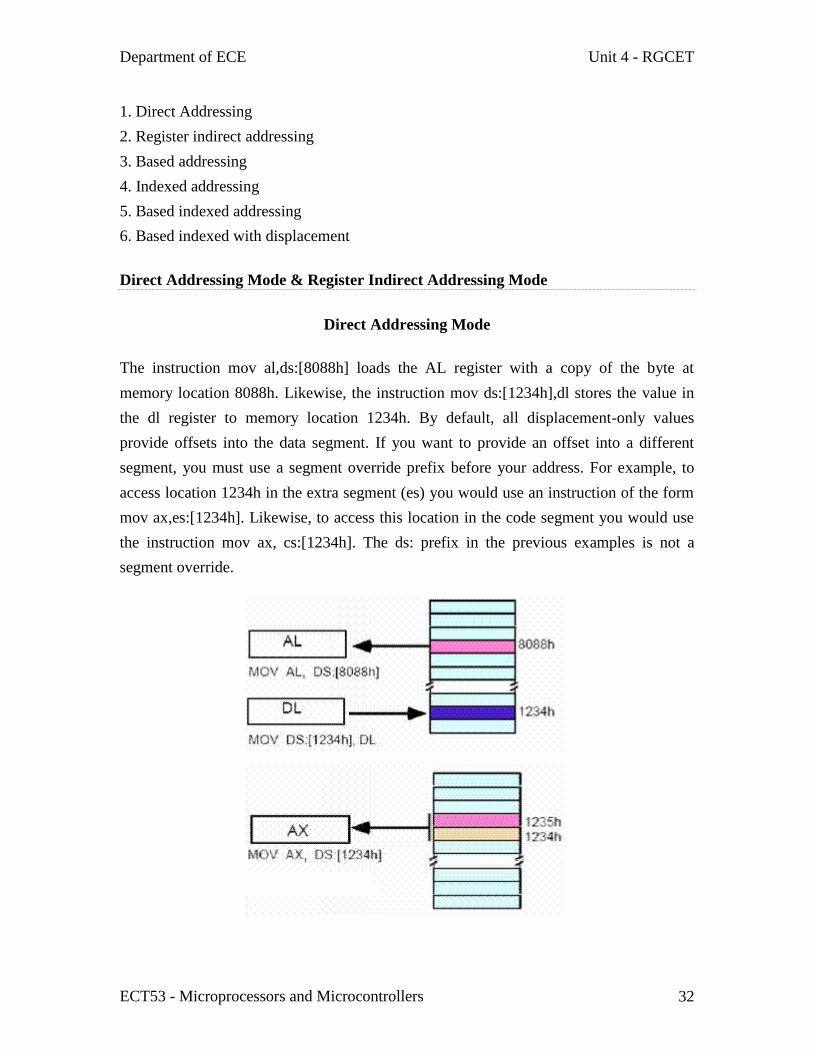
Department of ECE Unit 4 - RGCET
ECT53 - Microprocessors and Microcontrollers 39
Code segment (CS) is a 16-bit register containing address of 64 KB segment with
processor instructions The processor uses CS segment for all accesses to instructions
referenced by instruction pointer (IP) register CS register cannot be changed directly
The CS register is automatically updated during far jump far call and far return
instructions
Stack segment (SS) is a 16-bit register containing address of 64KB segment with
program stack By default the processor assumes that all data referenced by the stack
pointer (SP) and base pointer (BP) registers is located in the stack segment SS register
can be changed directly using POP instruction
Data segment (DS) is a 16-bit register containing address of 64KB segment with
program data By default the processor assumes that all data referenced by general
registers (AX BX CX DX) and index register (SI DI) is located in the data segment
DS register can be changed directly using POP and LDS instructions
Extra segment (ES) used to hold the starting address of Extra segment Extra segment is
provided for programs that need to access a second data segment Segment registers
cannot be used in arithmetic operations
Other registers of 8086
Instruction Pointer (IP) is a 16-bit register This is a crucially important register which
is used to control which instruction the CPU executes The ip or program counter is used
to store the memory location of the next instruction to be executed The CPU checks the
program counter to ascertain which instruction to carry out next It then updates the
program counter to point to the next instruction Thus the program counter will always
point to the next instruction to be executed
Flag Register contains a group of status bits called flags that indicate the status of the
CPU or the result of arithmetic operations There are two types of flags
Department of ECE Unit 4 - RGCET
ECT53 - Microprocessors and Microcontrollers 40
1 The status flags which reflect the result of executing an instruction The programmer
cannot setreset these flags directly
2 The control flags enable or disable certain CPU operations The programmer can
setreset these bits to control the CPUs operation
Nine individual bits of the status register are used as control flags (3 of them) and status
flags (6 of them)The remaining 7 are not used
A flag can only take on the values 0 and 1 We say a flag is set if it has the value 1The
status flags are used to record specific characteristics of arithmetic and of logical
instructions
Control Flags There are three control flags
1 The Direction Flag (D) Affects the direction of moving data blocks by such
instructions as MOVS CMPS and SCAS The flag values are 0 = up and 1 = down and
can be setreset by the STD (set D) and CLD (clear D) instructions
2 The Interrupt Flag (I) Dictates whether or not system interrupts can occur Interrupts
are actions initiated by hardware block such as input devices that will interrupt the
normal execution of programs The flag values are 0 = disable interrupts or 1 = enable
interrupts and can be manipulated by the CLI (clear I) and STI (set I) instructions
Department of ECE Unit 4 - RGCET
ECT53 - Microprocessors and Microcontrollers 41
3 The Trap Flag (T) Determines whether or not the CPU is halted after the execution
of each instruction When this flag is set (ie = 1) the programmer can single step
through his program to debug any errors When this flag = 0 this feature is off This flag
can be set by the INT 3 instruction
Status Flags There are six status flags
1 The Carry Flag (C) This flag is set when the result of an unsigned arithmetic
operation is too large to fit in the destination register This happens when there is an end
carry in an addition operation or there an end borrows in a subtraction operation A value
of 1 = carry and 0 = no carry
2 The Overflow Flag (O) This flag is set when the result of a signed arithmetic
operation is too large to fit in the destination register (ie when an overflow occurs)
Overflow can occur when adding two numbers with the same sign (ie both positive or
both negative) A value of 1 = overflow and 0 = no overflow
3 The Sign Flag (S) This flag is set when the result of an arithmetic or logic operation
is negative This flag is a copy of the MSB of the result (ie the sign bit) A value of 1
means negative and 0 = positive
4 The Zero Flag (Z) This flag is set when the result of an arithmetic or logic operation
is equal to zero A value of 1 means the result is zero and a value of 0 means the result is
not zero
5 The Auxiliary Carry Flag (A) This flag is set when an operation causes a carry from
bit 3 to bit 4 (or a borrow from bit 4 to bit 3) of an operand A value of 1 = carry and 0 =
no carry
6 The Parity Flag (P) This flags reflects the number of 1s in the result of an operation
If the number of 1s is even its value = 1 and if the number of 1s is odd then its value = 0
36 8086 Instruction Set and its Classification
The instructions of 8086 are classified into SIX groups They are
1 DATA TRANSFER INSTRUCTIONS
Department of ECE Unit 4 - RGCET
ECT53 - Microprocessors and Microcontrollers 42
2 ARITHMETIC INSTRUCTIONS
3 BIT MANIPULATION INSTRUCTIONS
4 STRING INSTRUCTIONS
5 PROGRAM EXECUTION TRANSFER INSTRUCTIONS
6 PROCESS CONTROL INSTRUCTIONS
1DATA TRANSFER INSTRUCTIONS
The DATA TRANSFER INSTRUCTIONS are those which transfers the DATA from
any one source to any one destinationThe datas may be of any type They are again
classified into four groupsThey are
GENERAL ndash PURPOSE
BYTE OR WORD
TRANSFER INSTRUCTIONS
SIMPLE INPUT AND
OUTPUT PORT
TRANSFER
INSTRUCTION
SPECIAL ADDRESS
TRANSFER
INSTRUCTION
FLAG
TRANSFER
INSTRUCTIONS
MOV
PUSH
POP
XCHG
XLAT
IN
OUT
LEA
LDS
LES
LAHF
SAHF
PUSHF
POPF
2ARITHMETIC INSTRUCTIONS
These instructions are those which are useful to perform Arithmetic calculations such as
addition subtraction multiplication and divisionThey are again classified into four
groupsThey are
ADDITION
INSTRUCTIONS
SUBTRACTION
INSTRUCTIONS
MULTIPLICATION
INSTRUCTIONS
DIVISION
INSTRUCTIONS
ADD
ADC
INC
AAA
DAA
SUB
SBB
DEC
NEG
CMP
AAS
DAS
MUL
IMUL
AAM
DIV
IDIV
AAD
CBW
CWD
3BIT MANIPULATION INSTRUCTIONS
Department of ECE Unit 4 - RGCET
ECT53 - Microprocessors and Microcontrollers 43
These instructions are used to perform Bit wise operations
LOGICAL INSTRUCTIONS SHIFT INSTRUCTIONS ROTATE INSTRUCTIONS
NOT
AND
OR
XOR
TEST
SHL SAL
SHR
SAR
ROL
ROR
RCL
RCR
4 STRING INSTRUCTIONS
The string instructions function easily on blocks of memoryThey are user friendly
instructions which help for easy program writing and execution They can speed up the
manipulating codeThey are useful in array handling tables and records
STRING INSTRUCTIONS
REP
REPE REPZ
REPNE REPNZ
MOVS MOVSB MOVSW
COMPS COMPSB
COMPSW
SCAS SCASB SCASW
LODS LODSB LODSW
STOS STOSB STOSW
5PROGRAM EXECUTION TRANSFER INSTRUCTIONS
These instructions transfer the program control from one address to other address ( Not
in a sequence) They are again classified into four groupsThey are
UNCONDITIONAL
TRANSFER
INSTRUCTIONS
CONDITIONAL
TRANSFER
INSTRUCTIONS
ITERATION CONTROL
INSTRUCTIONS
INTERRUPT
INSTRUCTIONS
CALL
RET
JMP
JA JNBE
JAE JNB
JB JNAE
JBE JNA
JC
JE JZ
JLE JNG
JNC
JNE JNZ
JNO
JNP JPO
JNS
LOOP
LOOPE LOOPZ
LOOPNE LOOPNZ
JCXZ
INT
INTO
IRET
Department of ECE Unit 4 - RGCET
ECT53 - Microprocessors and Microcontrollers 44
JG JNLE
JGE JNL
JL JNGE
JO
JP JPE
JS
6PROCESS CONTROL INSTRUCTIONS
These instructions are used to change the process of the Microprocessor They change the
process with the stored information They are again classified into Two groupsThey are
FLAG SET CLEAR
INSTRUCTIONS
EXTERNAL HARDWARE
SYNCHRONIZATION
INSTRUCTIONS
STC
CLC
CMC
STD
CLD
STI
CLI
HLT
WAIT
ESC
LOCK
NOP
37 Interrupts
Definition The meaning of lsquointerruptsrsquo is to break the sequence of operationWhile the
cpu is executing a programon lsquointerruptrsquo breaks the normal sequence of execution of
instructions diverts its execution to some other program called Interrupt Service Routine
(ISR)After executing ISR the control is transferred back again to the main
programInterrupt processing is an alternative to polling
Need for Interrupt Interrupts are particularly useful when interfacing IO devices that
provide or require data at relatively low data transfer rate
Types of Interrupts There are two types of Interrupts in 8086 They are
(i)Hardware Interrupts and
(ii)Software Interrupts
Department of ECE Unit 4 - RGCET
ECT53 - Microprocessors and Microcontrollers 45
(i) Hardware Interrupts (External Interrupts) The Intel microprocessors support
hardware interrupts through
Two pins that allow interrupt requests INTR and NMI
One pin that acknowledges INTA the interrupt requested on INTR
INTR and NMI
INTR is a maskable hardware interrupt The interrupt can be enableddisabled
using STICLI instructions or using more complicated method of updating the
FLAGS register with the help of the POPF instruction
When an interrupt occurs the processor stores FLAGS register into stack
disables further interrupts fetches from the bus one byte representing interrupt
type and jumps to interrupt processing routine address of which is stored in
location 4 ltinterrupt typegt Interrupt processing routine should return with the
IRET instruction
NMI is a non-maskable interrupt Interrupt is processed in the same way as the
INTR interrupt Interrupt type of the NMI is 2 ie the address of the NMI
processing routine is stored in location 0008h This interrupt has higher priority
than the maskable interrupt
ndash Ex NMI INTR
(ii) Software Interrupts (Internal Interrupts and Instructions) Software interrupts can
be caused by
INT instruction - breakpoint interrupt This is a type 3 interrupt
INT ltinterrupt numbergt instruction - any one interrupt from available 256
interrupts
INTO instruction - interrupt on overflow
Single-step interrupt - generated if the TF flag is set This is a type 1 interrupt
When the CPU processes this interrupt it clears TF flag before calling the
interrupt processing routine
Processor exceptions Divide Error (Type 0) Unused Opcode (type 6) and Escape
opcode (type 7)
Software interrupt processing is the same as for the hardware interrupts
Department of ECE Unit 4 - RGCET
ECT53 - Microprocessors and Microcontrollers 46
- Ex INT n (Software Instructions)
Control is provided through
o IF and TF flag bits
o IRET and IRETD
Performance of Hardware Interrupts
NMI Non maskable interrupts - TYPE 2 Interrupt
INTR Interrupt request - Between 20H and FFH
Interrupt Priority Structure
Performance of Software Interrupts
1 It decrements SP by 2 and pushes the flag register on the stack
2 Disables INTR by clearing the IF
3 It resets the TF in the flag Register
5 It decrements SP by 2 and pushes CS on the stack
Department of ECE Unit 4 - RGCET
ECT53 - Microprocessors and Microcontrollers 47
6 It decrements SP by 2 and pushes IP on the stack
6 Fetch the ISR address from the interrupt vector table
38 Other microprocessors the 80286 80386 and 80486 1048766 80286 Intel introduced 80286 in 1982
bull With 16-bit internal and external data bus
bull 24-bit address bus (224 = 16 megabyte)
bull virtual memory a way of fooling the microprocessor into thinking that it has access to
unlimited
memory by swapping data between disk storage and RAM
bull Real mode (faster operation with maximum of 1 Mbytes of memory) vs Protected
mode
protecting the operating system for accidental or deliberate destruction of the user
Protected
mode is slower but can use 16 Mbytes of memory
1048766 80386 introduced in 1985 also known as (80386DX)
bull With 32-bit internal and external data bus
bull 32-bit address bus (232 = 4 gigabyte-physical memory) With virtual memory 64
terabytes(246)
bull 80386SX was later introduced with the same internal structure with 16-bit external data
bus and
24-bit address bus 80386SX was much cheaper
1048766 All microprocessors discussed so far were general-purpose microprocessors and could
not handle
mathematical operations rapidly For this reason 8087 80287 80387 numeric data
processing chips
called math co-processors were used
1048766 80486 introduced in 1989 with 32-bit internal-external data bus and 32-bit address
bus
bull built in math co-processor in a single chip
bull Introduction of cache memory ( Static RAM with very fast access time)
Evolution of Intels Microprocessors
Department of ECE Unit 4 - RGCET
ECT53 - Microprocessors and Microcontrollers 41
3 The Trap Flag (T) Determines whether or not the CPU is halted after the execution
of each instruction When this flag is set (ie = 1) the programmer can single step
through his program to debug any errors When this flag = 0 this feature is off This flag
can be set by the INT 3 instruction
Status Flags There are six status flags
1 The Carry Flag (C) This flag is set when the result of an unsigned arithmetic
operation is too large to fit in the destination register This happens when there is an end
carry in an addition operation or there an end borrows in a subtraction operation A value
of 1 = carry and 0 = no carry
2 The Overflow Flag (O) This flag is set when the result of a signed arithmetic
operation is too large to fit in the destination register (ie when an overflow occurs)
Overflow can occur when adding two numbers with the same sign (ie both positive or
both negative) A value of 1 = overflow and 0 = no overflow
3 The Sign Flag (S) This flag is set when the result of an arithmetic or logic operation
is negative This flag is a copy of the MSB of the result (ie the sign bit) A value of 1
means negative and 0 = positive
4 The Zero Flag (Z) This flag is set when the result of an arithmetic or logic operation
is equal to zero A value of 1 means the result is zero and a value of 0 means the result is
not zero
5 The Auxiliary Carry Flag (A) This flag is set when an operation causes a carry from
bit 3 to bit 4 (or a borrow from bit 4 to bit 3) of an operand A value of 1 = carry and 0 =
no carry
6 The Parity Flag (P) This flags reflects the number of 1s in the result of an operation
If the number of 1s is even its value = 1 and if the number of 1s is odd then its value = 0
36 8086 Instruction Set and its Classification
The instructions of 8086 are classified into SIX groups They are
1 DATA TRANSFER INSTRUCTIONS
Department of ECE Unit 4 - RGCET
ECT53 - Microprocessors and Microcontrollers 42
2 ARITHMETIC INSTRUCTIONS
3 BIT MANIPULATION INSTRUCTIONS
4 STRING INSTRUCTIONS
5 PROGRAM EXECUTION TRANSFER INSTRUCTIONS
6 PROCESS CONTROL INSTRUCTIONS
1DATA TRANSFER INSTRUCTIONS
The DATA TRANSFER INSTRUCTIONS are those which transfers the DATA from
any one source to any one destinationThe datas may be of any type They are again
classified into four groupsThey are
GENERAL ndash PURPOSE
BYTE OR WORD
TRANSFER INSTRUCTIONS
SIMPLE INPUT AND
OUTPUT PORT
TRANSFER
INSTRUCTION
SPECIAL ADDRESS
TRANSFER
INSTRUCTION
FLAG
TRANSFER
INSTRUCTIONS
MOV
PUSH
POP
XCHG
XLAT
IN
OUT
LEA
LDS
LES
LAHF
SAHF
PUSHF
POPF
2ARITHMETIC INSTRUCTIONS
These instructions are those which are useful to perform Arithmetic calculations such as
addition subtraction multiplication and divisionThey are again classified into four
groupsThey are
ADDITION
INSTRUCTIONS
SUBTRACTION
INSTRUCTIONS
MULTIPLICATION
INSTRUCTIONS
DIVISION
INSTRUCTIONS
ADD
ADC
INC
AAA
DAA
SUB
SBB
DEC
NEG
CMP
AAS
DAS
MUL
IMUL
AAM
DIV
IDIV
AAD
CBW
CWD
3BIT MANIPULATION INSTRUCTIONS
Department of ECE Unit 4 - RGCET
ECT53 - Microprocessors and Microcontrollers 43
These instructions are used to perform Bit wise operations
LOGICAL INSTRUCTIONS SHIFT INSTRUCTIONS ROTATE INSTRUCTIONS
NOT
AND
OR
XOR
TEST
SHL SAL
SHR
SAR
ROL
ROR
RCL
RCR
4 STRING INSTRUCTIONS
The string instructions function easily on blocks of memoryThey are user friendly
instructions which help for easy program writing and execution They can speed up the
manipulating codeThey are useful in array handling tables and records
STRING INSTRUCTIONS
REP
REPE REPZ
REPNE REPNZ
MOVS MOVSB MOVSW
COMPS COMPSB
COMPSW
SCAS SCASB SCASW
LODS LODSB LODSW
STOS STOSB STOSW
5PROGRAM EXECUTION TRANSFER INSTRUCTIONS
These instructions transfer the program control from one address to other address ( Not
in a sequence) They are again classified into four groupsThey are
UNCONDITIONAL
TRANSFER
INSTRUCTIONS
CONDITIONAL
TRANSFER
INSTRUCTIONS
ITERATION CONTROL
INSTRUCTIONS
INTERRUPT
INSTRUCTIONS
CALL
RET
JMP
JA JNBE
JAE JNB
JB JNAE
JBE JNA
JC
JE JZ
JLE JNG
JNC
JNE JNZ
JNO
JNP JPO
JNS
LOOP
LOOPE LOOPZ
LOOPNE LOOPNZ
JCXZ
INT
INTO
IRET
Department of ECE Unit 4 - RGCET
ECT53 - Microprocessors and Microcontrollers 44
JG JNLE
JGE JNL
JL JNGE
JO
JP JPE
JS
6PROCESS CONTROL INSTRUCTIONS
These instructions are used to change the process of the Microprocessor They change the
process with the stored information They are again classified into Two groupsThey are
FLAG SET CLEAR
INSTRUCTIONS
EXTERNAL HARDWARE
SYNCHRONIZATION
INSTRUCTIONS
STC
CLC
CMC
STD
CLD
STI
CLI
HLT
WAIT
ESC
LOCK
NOP
37 Interrupts
Definition The meaning of lsquointerruptsrsquo is to break the sequence of operationWhile the
cpu is executing a programon lsquointerruptrsquo breaks the normal sequence of execution of
instructions diverts its execution to some other program called Interrupt Service Routine
(ISR)After executing ISR the control is transferred back again to the main
programInterrupt processing is an alternative to polling
Need for Interrupt Interrupts are particularly useful when interfacing IO devices that
provide or require data at relatively low data transfer rate
Types of Interrupts There are two types of Interrupts in 8086 They are
(i)Hardware Interrupts and
(ii)Software Interrupts
Department of ECE Unit 4 - RGCET
ECT53 - Microprocessors and Microcontrollers 45
(i) Hardware Interrupts (External Interrupts) The Intel microprocessors support
hardware interrupts through
Two pins that allow interrupt requests INTR and NMI
One pin that acknowledges INTA the interrupt requested on INTR
INTR and NMI
INTR is a maskable hardware interrupt The interrupt can be enableddisabled
using STICLI instructions or using more complicated method of updating the
FLAGS register with the help of the POPF instruction
When an interrupt occurs the processor stores FLAGS register into stack
disables further interrupts fetches from the bus one byte representing interrupt
type and jumps to interrupt processing routine address of which is stored in
location 4 ltinterrupt typegt Interrupt processing routine should return with the
IRET instruction
NMI is a non-maskable interrupt Interrupt is processed in the same way as the
INTR interrupt Interrupt type of the NMI is 2 ie the address of the NMI
processing routine is stored in location 0008h This interrupt has higher priority
than the maskable interrupt
ndash Ex NMI INTR
(ii) Software Interrupts (Internal Interrupts and Instructions) Software interrupts can
be caused by
INT instruction - breakpoint interrupt This is a type 3 interrupt
INT ltinterrupt numbergt instruction - any one interrupt from available 256
interrupts
INTO instruction - interrupt on overflow
Single-step interrupt - generated if the TF flag is set This is a type 1 interrupt
When the CPU processes this interrupt it clears TF flag before calling the
interrupt processing routine
Processor exceptions Divide Error (Type 0) Unused Opcode (type 6) and Escape
opcode (type 7)
Software interrupt processing is the same as for the hardware interrupts
Department of ECE Unit 4 - RGCET
ECT53 - Microprocessors and Microcontrollers 46
- Ex INT n (Software Instructions)
Control is provided through
o IF and TF flag bits
o IRET and IRETD
Performance of Hardware Interrupts
NMI Non maskable interrupts - TYPE 2 Interrupt
INTR Interrupt request - Between 20H and FFH
Interrupt Priority Structure
Performance of Software Interrupts
1 It decrements SP by 2 and pushes the flag register on the stack
2 Disables INTR by clearing the IF
3 It resets the TF in the flag Register
5 It decrements SP by 2 and pushes CS on the stack
Department of ECE Unit 4 - RGCET
ECT53 - Microprocessors and Microcontrollers 47
6 It decrements SP by 2 and pushes IP on the stack
6 Fetch the ISR address from the interrupt vector table
38 Other microprocessors the 80286 80386 and 80486 1048766 80286 Intel introduced 80286 in 1982
bull With 16-bit internal and external data bus
bull 24-bit address bus (224 = 16 megabyte)
bull virtual memory a way of fooling the microprocessor into thinking that it has access to
unlimited
memory by swapping data between disk storage and RAM
bull Real mode (faster operation with maximum of 1 Mbytes of memory) vs Protected
mode
protecting the operating system for accidental or deliberate destruction of the user
Protected
mode is slower but can use 16 Mbytes of memory
1048766 80386 introduced in 1985 also known as (80386DX)
bull With 32-bit internal and external data bus
bull 32-bit address bus (232 = 4 gigabyte-physical memory) With virtual memory 64
terabytes(246)
bull 80386SX was later introduced with the same internal structure with 16-bit external data
bus and
24-bit address bus 80386SX was much cheaper
1048766 All microprocessors discussed so far were general-purpose microprocessors and could
not handle
mathematical operations rapidly For this reason 8087 80287 80387 numeric data
processing chips
called math co-processors were used
1048766 80486 introduced in 1989 with 32-bit internal-external data bus and 32-bit address
bus
bull built in math co-processor in a single chip
bull Introduction of cache memory ( Static RAM with very fast access time)
Evolution of Intels Microprocessors

Department of ECE Unit 4 - RGCET
ECT53 - Microprocessors and Microcontrollers 43
These instructions are used to perform Bit wise operations
LOGICAL INSTRUCTIONS SHIFT INSTRUCTIONS ROTATE INSTRUCTIONS
NOT
AND
OR
XOR
TEST
SHL SAL
SHR
SAR
ROL
ROR
RCL
RCR
4 STRING INSTRUCTIONS
The string instructions function easily on blocks of memoryThey are user friendly
instructions which help for easy program writing and execution They can speed up the
manipulating codeThey are useful in array handling tables and records
STRING INSTRUCTIONS
REP
REPE REPZ
REPNE REPNZ
MOVS MOVSB MOVSW
COMPS COMPSB
COMPSW
SCAS SCASB SCASW
LODS LODSB LODSW
STOS STOSB STOSW
5PROGRAM EXECUTION TRANSFER INSTRUCTIONS
These instructions transfer the program control from one address to other address ( Not
in a sequence) They are again classified into four groupsThey are
UNCONDITIONAL
TRANSFER
INSTRUCTIONS
CONDITIONAL
TRANSFER
INSTRUCTIONS
ITERATION CONTROL
INSTRUCTIONS
INTERRUPT
INSTRUCTIONS
CALL
RET
JMP
JA JNBE
JAE JNB
JB JNAE
JBE JNA
JC
JE JZ
JLE JNG
JNC
JNE JNZ
JNO
JNP JPO
JNS
LOOP
LOOPE LOOPZ
LOOPNE LOOPNZ
JCXZ
INT
INTO
IRET
Department of ECE Unit 4 - RGCET
ECT53 - Microprocessors and Microcontrollers 44
JG JNLE
JGE JNL
JL JNGE
JO
JP JPE
JS
6PROCESS CONTROL INSTRUCTIONS
These instructions are used to change the process of the Microprocessor They change the
process with the stored information They are again classified into Two groupsThey are
FLAG SET CLEAR
INSTRUCTIONS
EXTERNAL HARDWARE
SYNCHRONIZATION
INSTRUCTIONS
STC
CLC
CMC
STD
CLD
STI
CLI
HLT
WAIT
ESC
LOCK
NOP
37 Interrupts
Definition The meaning of lsquointerruptsrsquo is to break the sequence of operationWhile the
cpu is executing a programon lsquointerruptrsquo breaks the normal sequence of execution of
instructions diverts its execution to some other program called Interrupt Service Routine
(ISR)After executing ISR the control is transferred back again to the main
programInterrupt processing is an alternative to polling
Need for Interrupt Interrupts are particularly useful when interfacing IO devices that
provide or require data at relatively low data transfer rate
Types of Interrupts There are two types of Interrupts in 8086 They are
(i)Hardware Interrupts and
(ii)Software Interrupts
Department of ECE Unit 4 - RGCET
ECT53 - Microprocessors and Microcontrollers 45
(i) Hardware Interrupts (External Interrupts) The Intel microprocessors support
hardware interrupts through
Two pins that allow interrupt requests INTR and NMI
One pin that acknowledges INTA the interrupt requested on INTR
INTR and NMI
INTR is a maskable hardware interrupt The interrupt can be enableddisabled
using STICLI instructions or using more complicated method of updating the
FLAGS register with the help of the POPF instruction
When an interrupt occurs the processor stores FLAGS register into stack
disables further interrupts fetches from the bus one byte representing interrupt
type and jumps to interrupt processing routine address of which is stored in
location 4 ltinterrupt typegt Interrupt processing routine should return with the
IRET instruction
NMI is a non-maskable interrupt Interrupt is processed in the same way as the
INTR interrupt Interrupt type of the NMI is 2 ie the address of the NMI
processing routine is stored in location 0008h This interrupt has higher priority
than the maskable interrupt
ndash Ex NMI INTR
(ii) Software Interrupts (Internal Interrupts and Instructions) Software interrupts can
be caused by
INT instruction - breakpoint interrupt This is a type 3 interrupt
INT ltinterrupt numbergt instruction - any one interrupt from available 256
interrupts
INTO instruction - interrupt on overflow
Single-step interrupt - generated if the TF flag is set This is a type 1 interrupt
When the CPU processes this interrupt it clears TF flag before calling the
interrupt processing routine
Processor exceptions Divide Error (Type 0) Unused Opcode (type 6) and Escape
opcode (type 7)
Software interrupt processing is the same as for the hardware interrupts
Department of ECE Unit 4 - RGCET
ECT53 - Microprocessors and Microcontrollers 46
- Ex INT n (Software Instructions)
Control is provided through
o IF and TF flag bits
o IRET and IRETD
Performance of Hardware Interrupts
NMI Non maskable interrupts - TYPE 2 Interrupt
INTR Interrupt request - Between 20H and FFH
Interrupt Priority Structure
Performance of Software Interrupts
1 It decrements SP by 2 and pushes the flag register on the stack
2 Disables INTR by clearing the IF
3 It resets the TF in the flag Register
5 It decrements SP by 2 and pushes CS on the stack
Department of ECE Unit 4 - RGCET
ECT53 - Microprocessors and Microcontrollers 47
6 It decrements SP by 2 and pushes IP on the stack
6 Fetch the ISR address from the interrupt vector table
38 Other microprocessors the 80286 80386 and 80486 1048766 80286 Intel introduced 80286 in 1982
bull With 16-bit internal and external data bus
bull 24-bit address bus (224 = 16 megabyte)
bull virtual memory a way of fooling the microprocessor into thinking that it has access to
unlimited
memory by swapping data between disk storage and RAM
bull Real mode (faster operation with maximum of 1 Mbytes of memory) vs Protected
mode
protecting the operating system for accidental or deliberate destruction of the user
Protected
mode is slower but can use 16 Mbytes of memory
1048766 80386 introduced in 1985 also known as (80386DX)
bull With 32-bit internal and external data bus
bull 32-bit address bus (232 = 4 gigabyte-physical memory) With virtual memory 64
terabytes(246)
bull 80386SX was later introduced with the same internal structure with 16-bit external data
bus and
24-bit address bus 80386SX was much cheaper
1048766 All microprocessors discussed so far were general-purpose microprocessors and could
not handle
mathematical operations rapidly For this reason 8087 80287 80387 numeric data
processing chips
called math co-processors were used
1048766 80486 introduced in 1989 with 32-bit internal-external data bus and 32-bit address
bus
bull built in math co-processor in a single chip
bull Introduction of cache memory ( Static RAM with very fast access time)
Evolution of Intels Microprocessors
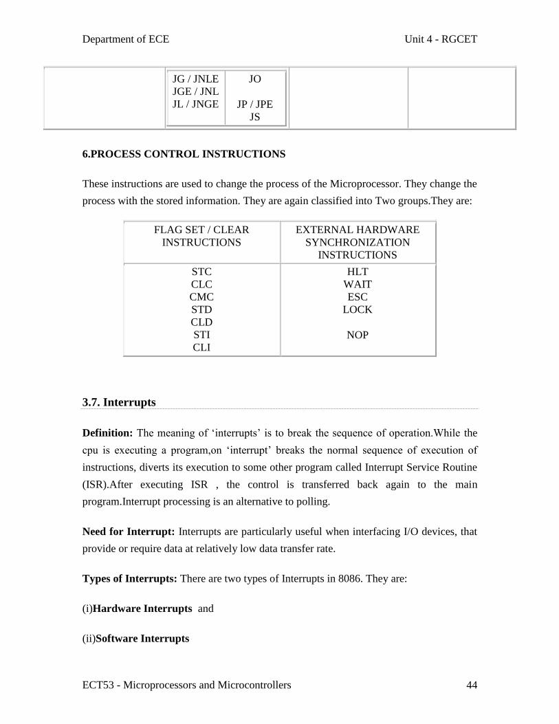
Department of ECE Unit 4 - RGCET
ECT53 - Microprocessors and Microcontrollers 44
JG JNLE
JGE JNL
JL JNGE
JO
JP JPE
JS
6PROCESS CONTROL INSTRUCTIONS
These instructions are used to change the process of the Microprocessor They change the
process with the stored information They are again classified into Two groupsThey are
FLAG SET CLEAR
INSTRUCTIONS
EXTERNAL HARDWARE
SYNCHRONIZATION
INSTRUCTIONS
STC
CLC
CMC
STD
CLD
STI
CLI
HLT
WAIT
ESC
LOCK
NOP
37 Interrupts
Definition The meaning of lsquointerruptsrsquo is to break the sequence of operationWhile the
cpu is executing a programon lsquointerruptrsquo breaks the normal sequence of execution of
instructions diverts its execution to some other program called Interrupt Service Routine
(ISR)After executing ISR the control is transferred back again to the main
programInterrupt processing is an alternative to polling
Need for Interrupt Interrupts are particularly useful when interfacing IO devices that
provide or require data at relatively low data transfer rate
Types of Interrupts There are two types of Interrupts in 8086 They are
(i)Hardware Interrupts and
(ii)Software Interrupts
Department of ECE Unit 4 - RGCET
ECT53 - Microprocessors and Microcontrollers 45
(i) Hardware Interrupts (External Interrupts) The Intel microprocessors support
hardware interrupts through
Two pins that allow interrupt requests INTR and NMI
One pin that acknowledges INTA the interrupt requested on INTR
INTR and NMI
INTR is a maskable hardware interrupt The interrupt can be enableddisabled
using STICLI instructions or using more complicated method of updating the
FLAGS register with the help of the POPF instruction
When an interrupt occurs the processor stores FLAGS register into stack
disables further interrupts fetches from the bus one byte representing interrupt
type and jumps to interrupt processing routine address of which is stored in
location 4 ltinterrupt typegt Interrupt processing routine should return with the
IRET instruction
NMI is a non-maskable interrupt Interrupt is processed in the same way as the
INTR interrupt Interrupt type of the NMI is 2 ie the address of the NMI
processing routine is stored in location 0008h This interrupt has higher priority
than the maskable interrupt
ndash Ex NMI INTR
(ii) Software Interrupts (Internal Interrupts and Instructions) Software interrupts can
be caused by
INT instruction - breakpoint interrupt This is a type 3 interrupt
INT ltinterrupt numbergt instruction - any one interrupt from available 256
interrupts
INTO instruction - interrupt on overflow
Single-step interrupt - generated if the TF flag is set This is a type 1 interrupt
When the CPU processes this interrupt it clears TF flag before calling the
interrupt processing routine
Processor exceptions Divide Error (Type 0) Unused Opcode (type 6) and Escape
opcode (type 7)
Software interrupt processing is the same as for the hardware interrupts
Department of ECE Unit 4 - RGCET
ECT53 - Microprocessors and Microcontrollers 46
- Ex INT n (Software Instructions)
Control is provided through
o IF and TF flag bits
o IRET and IRETD
Performance of Hardware Interrupts
NMI Non maskable interrupts - TYPE 2 Interrupt
INTR Interrupt request - Between 20H and FFH
Interrupt Priority Structure
Performance of Software Interrupts
1 It decrements SP by 2 and pushes the flag register on the stack
2 Disables INTR by clearing the IF
3 It resets the TF in the flag Register
5 It decrements SP by 2 and pushes CS on the stack
Department of ECE Unit 4 - RGCET
ECT53 - Microprocessors and Microcontrollers 47
6 It decrements SP by 2 and pushes IP on the stack
6 Fetch the ISR address from the interrupt vector table
38 Other microprocessors the 80286 80386 and 80486 1048766 80286 Intel introduced 80286 in 1982
bull With 16-bit internal and external data bus
bull 24-bit address bus (224 = 16 megabyte)
bull virtual memory a way of fooling the microprocessor into thinking that it has access to
unlimited
memory by swapping data between disk storage and RAM
bull Real mode (faster operation with maximum of 1 Mbytes of memory) vs Protected
mode
protecting the operating system for accidental or deliberate destruction of the user
Protected
mode is slower but can use 16 Mbytes of memory
1048766 80386 introduced in 1985 also known as (80386DX)
bull With 32-bit internal and external data bus
bull 32-bit address bus (232 = 4 gigabyte-physical memory) With virtual memory 64
terabytes(246)
bull 80386SX was later introduced with the same internal structure with 16-bit external data
bus and
24-bit address bus 80386SX was much cheaper
1048766 All microprocessors discussed so far were general-purpose microprocessors and could
not handle
mathematical operations rapidly For this reason 8087 80287 80387 numeric data
processing chips
called math co-processors were used
1048766 80486 introduced in 1989 with 32-bit internal-external data bus and 32-bit address
bus
bull built in math co-processor in a single chip
bull Introduction of cache memory ( Static RAM with very fast access time)
Evolution of Intels Microprocessors
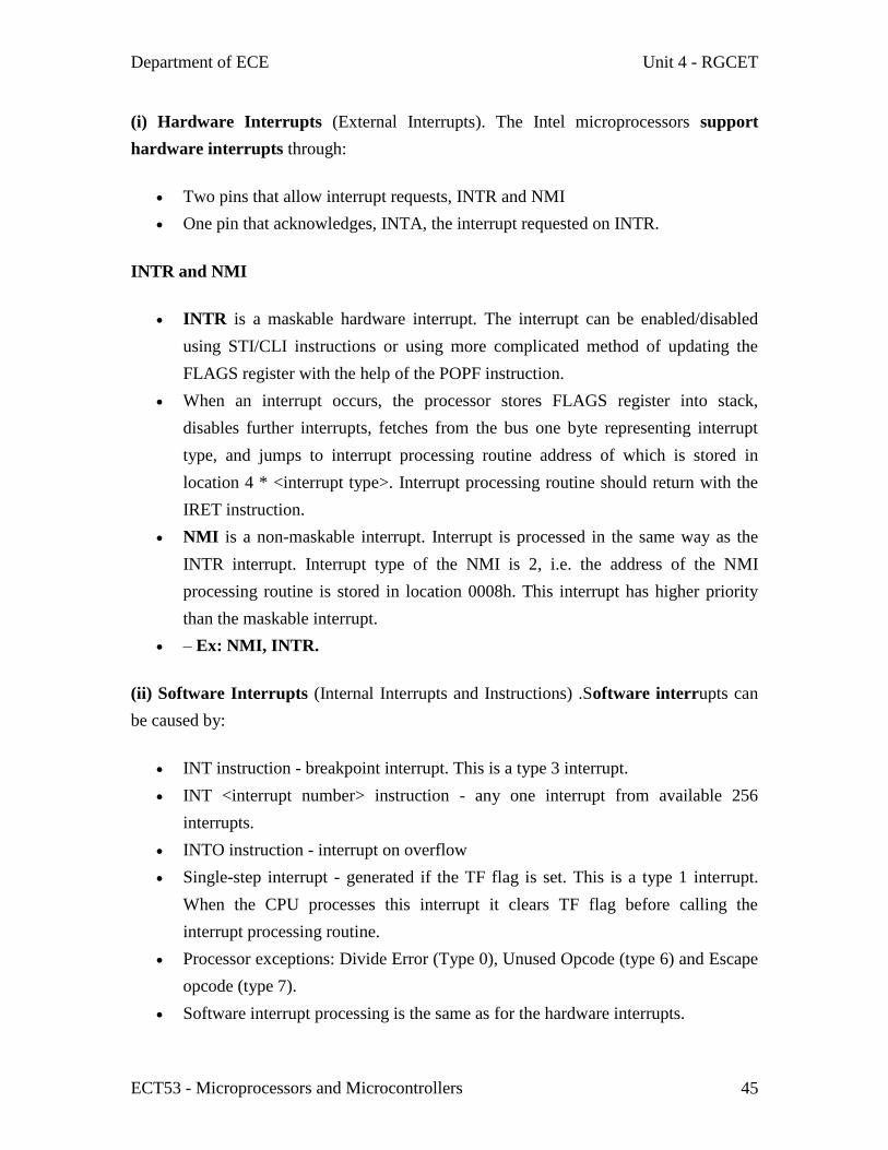
Department of ECE Unit 4 - RGCET
ECT53 - Microprocessors and Microcontrollers 45
(i) Hardware Interrupts (External Interrupts) The Intel microprocessors support
hardware interrupts through
Two pins that allow interrupt requests INTR and NMI
One pin that acknowledges INTA the interrupt requested on INTR
INTR and NMI
INTR is a maskable hardware interrupt The interrupt can be enableddisabled
using STICLI instructions or using more complicated method of updating the
FLAGS register with the help of the POPF instruction
When an interrupt occurs the processor stores FLAGS register into stack
disables further interrupts fetches from the bus one byte representing interrupt
type and jumps to interrupt processing routine address of which is stored in
location 4 ltinterrupt typegt Interrupt processing routine should return with the
IRET instruction
NMI is a non-maskable interrupt Interrupt is processed in the same way as the
INTR interrupt Interrupt type of the NMI is 2 ie the address of the NMI
processing routine is stored in location 0008h This interrupt has higher priority
than the maskable interrupt
ndash Ex NMI INTR
(ii) Software Interrupts (Internal Interrupts and Instructions) Software interrupts can
be caused by
INT instruction - breakpoint interrupt This is a type 3 interrupt
INT ltinterrupt numbergt instruction - any one interrupt from available 256
interrupts
INTO instruction - interrupt on overflow
Single-step interrupt - generated if the TF flag is set This is a type 1 interrupt
When the CPU processes this interrupt it clears TF flag before calling the
interrupt processing routine
Processor exceptions Divide Error (Type 0) Unused Opcode (type 6) and Escape
opcode (type 7)
Software interrupt processing is the same as for the hardware interrupts
Department of ECE Unit 4 - RGCET
ECT53 - Microprocessors and Microcontrollers 46
- Ex INT n (Software Instructions)
Control is provided through
o IF and TF flag bits
o IRET and IRETD
Performance of Hardware Interrupts
NMI Non maskable interrupts - TYPE 2 Interrupt
INTR Interrupt request - Between 20H and FFH
Interrupt Priority Structure
Performance of Software Interrupts
1 It decrements SP by 2 and pushes the flag register on the stack
2 Disables INTR by clearing the IF
3 It resets the TF in the flag Register
5 It decrements SP by 2 and pushes CS on the stack
Department of ECE Unit 4 - RGCET
ECT53 - Microprocessors and Microcontrollers 47
6 It decrements SP by 2 and pushes IP on the stack
6 Fetch the ISR address from the interrupt vector table
38 Other microprocessors the 80286 80386 and 80486 1048766 80286 Intel introduced 80286 in 1982
bull With 16-bit internal and external data bus
bull 24-bit address bus (224 = 16 megabyte)
bull virtual memory a way of fooling the microprocessor into thinking that it has access to
unlimited
memory by swapping data between disk storage and RAM
bull Real mode (faster operation with maximum of 1 Mbytes of memory) vs Protected
mode
protecting the operating system for accidental or deliberate destruction of the user
Protected
mode is slower but can use 16 Mbytes of memory
1048766 80386 introduced in 1985 also known as (80386DX)
bull With 32-bit internal and external data bus
bull 32-bit address bus (232 = 4 gigabyte-physical memory) With virtual memory 64
terabytes(246)
bull 80386SX was later introduced with the same internal structure with 16-bit external data
bus and
24-bit address bus 80386SX was much cheaper
1048766 All microprocessors discussed so far were general-purpose microprocessors and could
not handle
mathematical operations rapidly For this reason 8087 80287 80387 numeric data
processing chips
called math co-processors were used
1048766 80486 introduced in 1989 with 32-bit internal-external data bus and 32-bit address
bus
bull built in math co-processor in a single chip
bull Introduction of cache memory ( Static RAM with very fast access time)
Evolution of Intels Microprocessors
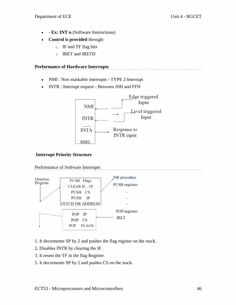
Department of ECE Unit 4 - RGCET
ECT53 - Microprocessors and Microcontrollers 46
- Ex INT n (Software Instructions)
Control is provided through
o IF and TF flag bits
o IRET and IRETD
Performance of Hardware Interrupts
NMI Non maskable interrupts - TYPE 2 Interrupt
INTR Interrupt request - Between 20H and FFH
Interrupt Priority Structure
Performance of Software Interrupts
1 It decrements SP by 2 and pushes the flag register on the stack
2 Disables INTR by clearing the IF
3 It resets the TF in the flag Register
5 It decrements SP by 2 and pushes CS on the stack
Department of ECE Unit 4 - RGCET
ECT53 - Microprocessors and Microcontrollers 47
6 It decrements SP by 2 and pushes IP on the stack
6 Fetch the ISR address from the interrupt vector table
38 Other microprocessors the 80286 80386 and 80486 1048766 80286 Intel introduced 80286 in 1982
bull With 16-bit internal and external data bus
bull 24-bit address bus (224 = 16 megabyte)
bull virtual memory a way of fooling the microprocessor into thinking that it has access to
unlimited
memory by swapping data between disk storage and RAM
bull Real mode (faster operation with maximum of 1 Mbytes of memory) vs Protected
mode
protecting the operating system for accidental or deliberate destruction of the user
Protected
mode is slower but can use 16 Mbytes of memory
1048766 80386 introduced in 1985 also known as (80386DX)
bull With 32-bit internal and external data bus
bull 32-bit address bus (232 = 4 gigabyte-physical memory) With virtual memory 64
terabytes(246)
bull 80386SX was later introduced with the same internal structure with 16-bit external data
bus and
24-bit address bus 80386SX was much cheaper
1048766 All microprocessors discussed so far were general-purpose microprocessors and could
not handle
mathematical operations rapidly For this reason 8087 80287 80387 numeric data
processing chips
called math co-processors were used
1048766 80486 introduced in 1989 with 32-bit internal-external data bus and 32-bit address
bus
bull built in math co-processor in a single chip
bull Introduction of cache memory ( Static RAM with very fast access time)
Evolution of Intels Microprocessors
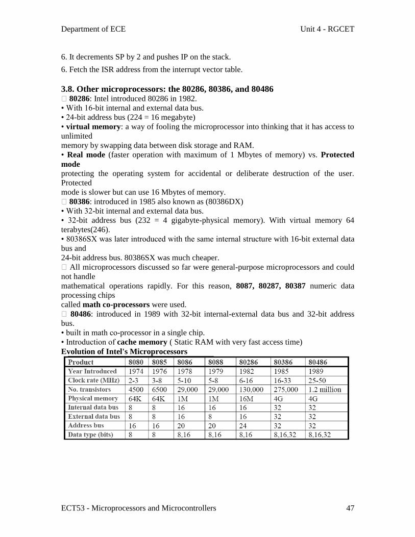
Department of ECE Unit 4 - RGCET
ECT53 - Microprocessors and Microcontrollers 47
6 It decrements SP by 2 and pushes IP on the stack
6 Fetch the ISR address from the interrupt vector table
38 Other microprocessors the 80286 80386 and 80486 1048766 80286 Intel introduced 80286 in 1982
bull With 16-bit internal and external data bus
bull 24-bit address bus (224 = 16 megabyte)
bull virtual memory a way of fooling the microprocessor into thinking that it has access to
unlimited
memory by swapping data between disk storage and RAM
bull Real mode (faster operation with maximum of 1 Mbytes of memory) vs Protected
mode
protecting the operating system for accidental or deliberate destruction of the user
Protected
mode is slower but can use 16 Mbytes of memory
1048766 80386 introduced in 1985 also known as (80386DX)
bull With 32-bit internal and external data bus
bull 32-bit address bus (232 = 4 gigabyte-physical memory) With virtual memory 64
terabytes(246)
bull 80386SX was later introduced with the same internal structure with 16-bit external data
bus and
24-bit address bus 80386SX was much cheaper
1048766 All microprocessors discussed so far were general-purpose microprocessors and could
not handle
mathematical operations rapidly For this reason 8087 80287 80387 numeric data
processing chips
called math co-processors were used
1048766 80486 introduced in 1989 with 32-bit internal-external data bus and 32-bit address
bus
bull built in math co-processor in a single chip
bull Introduction of cache memory ( Static RAM with very fast access time)
Evolution of Intels Microprocessors