p~eesiiest.weebly.com/uploads/2/6/9/2/26921317/part_-_4...12.2 rectangular waveguides • 545 as...
TRANSCRIPT

12.2 RECTANGULAR WAVEGUIDES • 545
As usual, if we assume that the wave propagates along the waveguide in the +z-direction,the multiplicative constant c5 = 0 because the wave has to be finite at infinity [i.e.,Ezs(x, y, z = °°) = 0]. Hence eq. (12.10) is reduced to
Ezs(x, y, z) = (A; cos k^x + A2 sin cos kyy + A4 sin kyy)e (12.11)
where Aj = CiC6, A2 = c2c6, and so on. By taking similar steps, we get the solution of thez-component of eq. (12.2) as
Hzs(x, y, z) = (Bi cos kpc + B2 sin ^ cos kyy + B4 sin kyy)e (12.12)
Instead of solving for other field component Exs, Eys, Hxs, and Hys in eqs. (12.1) and (12.2)in the same manner, we simply use Maxwell's equations to determine them from Ezs andHTS. From
and
V X E, = -y
V X H, = jtoeEs
we obtain
dE,<
dy
dHzs
dy
dExs
dz
dHxs
dz
dEys
dx
dHy,
dz
dHv,
dz
dx
dHz,
dx
9EX,
dy
dHx,
= jueExs
= J03flHys
dx dy
(12.13a)
(12.13b)
(12.13c)
(12.13d)
(12.13e)
(12.13f)
We will now express Exs, Eys, Hxs, and Hys in terms of Ezs and Hzs. For Exs, for example,we combine eqs. (12.13b) and (12.13c) and obtain
dHz, 1 fd2Exs d2Ez.
dy 7C0/X \ dz oxdi(12.14)
From eqs. (12.11) and (12.12), it is clear that all field components vary with z according toe~yz, that is,
p~lz F

546 • Waveguides
Hence
and eq. (12.14) becomes
dEzs d Exx ,— = ~yEzs, —j- = 7 EX:
dZ dz
dHa 1 { 2 dE^jweExs = —— + - — I 7 Exs + 7——
dy joifi \ dx
or
1 , 2 , 2 ^ r 7 dEzs dHzs
—.— (7 + " V ) Exs = ~. — + ——jii ju>n dx dy
Thus, if we let h2 = y2 + w2/xe = y2 + k2,
E 1 —- '__7 dEzs jun dHzs
hl dx dy
Similar manipulations of eq. (12.13) yield expressions for Eys, Hxs, and Hys in terms of Ev
and Hzs. Thus,
(12.15a)
(12.15b)
(12.15c)
(12.15d)
Exs
EyS
M
Hys
h2 dx
7 dEzs
h2 dy
_ jue dEzs _
h2 dy
_ ja>e dEzs
jan dHz,
h2 dy
ju/x dHzs
h2 dx
7 dHzs
h2 dx
~~h2^T
where
h2 = y2 + k2 = k2x + k] (12.16)
Thus we can use eq. (12.15) in conjunction with eqs. (12.11) and (12.12) to obtain Exs, Eys,Hxs, and Hys.
From eqs. (12.11), (12.12), and (12.15), we notice that there are different types of fieldpatterns or configurations. Each of these distinct field patterns is called a mode. Four dif-ferent mode categories can exist, namely:
1. Ea = 0 = Hzs (TEM mode): This is the transverse electromagnetic (TEM) mode,in which both the E and H fields are transverse to the direction of wave propaga-tion. From eq. (12.15), all field components vanish for Ezs = 0 = Hzs. Conse-quently, we conclude that a rectangular waveguide cannot support TEM mode.

12.3 TRANSVERSE MAGNETIC (TM) MODES 547
Figure 12.3 Components of EM fields in a rectangular waveguide:(a) TE mode Ez = 0, (b) TM mode, Hz = 0.
2. Ezs = 0, Hzs # 0 (TE modes): For this case, the remaining components (Exs andEys) of the electric field are transverse to the direction of propagation az. Under thiscondition, fields are said to be in transverse electric (TE) modes. See Figure12.3(a).
3. Ezs + 0, Hzs = 0 (TM modes): In this case, the H field is transverse to the directionof wave propagation. Thus we have transverse magnetic (TM) modes. See Figure12.3(b).
4. Ezs + 0, Hzs + 0 (HE modes): This is the case when neither E nor H field is trans-verse to the direction of wave propagation. They are sometimes referred to ashybrid modes.
We should note the relationship between k in eq. (12.3) and j3 of eq. (10.43a). Thephase constant /3 in eq. (10.43a) was derived for TEM mode. For the TEM mode, h = 0, sofrom eq. (12.16), y2 = -k2 -» y = a + j/3 = jk; that is, /3 = k. For other modes, j3 + k.In the subsequent sections, we shall examine the TM and TE modes of propagation sepa-rately.
2.3 TRANSVERSE MAGNETIC (TM) MODES
For this case, the magnetic field has its components transverse (or normal) to the directionof wave propagation. This implies that we set Hz = 0 and determine Ex, Ey, Ez, Hx, and Hv
using eqs. (12.11) and (12.15) and the boundary conditions. We shall solve for Ez and laterdetermine other field components from Ez. At the walls of the waveguide, the tangentialcomponents of the E field must be continuous; that is,
= 0 at y = 0
y = b£,, = 0 at
Ezs = 0 at x = 0
£„ = 0 at x = a
(12.17a)
(12.17b)
(12.17c)
(12.17d)

548 Waveguides
Equations (12.17a) and (12.17c) require that A, = 0 = A3 in eq. (12.11), so eq. (12.11)becomes
Ea = Eo sin kj sin kyy e~yz (12.18)
where Eo = A2A4. Also eqs. (12.17b) and (12.17d) when applied to eq. (12.18) require that
s i n ^ = 0, sinkyb = O (12.19)
This implies that
kxa = rrnr, m = 1 , 2 , 3 , . . . (12.20a)
kyb = nir, n = 1 , 2 , 3 , . . . (12.20b)
or
_ n7r
Ky —
b(12.21)
The negative integers are not chosen for m and n in eq. (12.20a) for the reason given inExample 6.5. Substituting eq. (12.21) into eq. (12.18) gives
E7. = Eo sin. fnnrx\ . fniry\ 'in cm — \ o <c '
V a I sinb ) '
(12.22)
We obtain other field components from eqs. (12.22) and (12.15) bearing in mind thatH7< = 0. Thus
(12.23a)
(12.23b)
(12.23c)
y fnw\ IT • fmirx\ (n*y\ -yz— ' — l F
o sin I I cos I I e T
jus
Hys = - v (-j-) Eo cos sin (12.23d)
where
nir (12.24)
which is obtained from eqs. (12.16) and (12.21). Notice from eqs. (12.22) and (12.23) thateach set of integers m and n gives a different field pattern or mode, referred to as TMmn

12.3 TRANSVERSE MAGNETIC (TM) MODES 549
mode, in the waveguide. Integer m equals the number of half-cycle variations in the x-direction, and integer n is the number of half-cycle variations in the v-direction. We alsonotice from eqs. (12.22) and (12.23) that if (m, n) is (0, 0), (0, n), or (m, 0), all field com-ponents vanish. Thus neither m nor n can be zero. Consequently, TMH is the lowest-ordermode of all the TMmn modes.
By substituting eq. (12.21) into eq. (12.16), we obtain the propagation constant
7 =mira
nir
b(12.25)
where k = u V ^ e as in eq. (12.3). We recall that, in general, y = a + j(3. In the case ofeq. (12.25), we have three possibilities depending on k (or w), m, and n:
CASE A (cutoff):
If
1c = w jus =[b
7 = 0 or a = 0 = /3
The value of w that causes this is called the cutoff angular frequency o)c; that is,
1 / U T T I 2 Tmr"12
I « J U (12.26)
CASE B (evanescent):
If
TOTTT]2 Tnir
y = a,
In this case, we have no wave propagation at all. These nonpropagating or attenuatingmodes are said to be evanescent.
CASE C (propagation):
If
^2 = oA mir
y =;/?, a = 0

550 Waveguides
that is, from eq. (12.25) the phase constant (3 becomes
0 = - -L a nir (12.27)
This is the only case when propagation takes place because all field components will havethe factor e'yz = e~jl3z.
Thus for each mode, characterized by a set of integers m and n, there is a correspond-ing cutoff frequency fc
The cutoff frequency is the operating frequencs below which allcnuaiion occursand above which propagation lakes place.
The waveguide therefore operates as a high-pass filter. The cutoff frequency is obtainedfromeq. (12.26) as
1
2-irVuennra
or
fc u/ / N
// mu \)+ / N/ nu\
(12.28)
where u' = = phase velocity of uniform plane wave in the lossless dielectricfie
medium (a = 0, fi, e) filling the waveguide. The cutoff wave length \. is given by
or
X = (12.29)
Note from eqs. (12.28) and (12.29) that TMn has the lowest cutoff frequency (or thelongest cutoff wavelength) of all the TM modes. The phase constant /3 in eq. (12.27) can bewritten in terms of fc as
= wV/xs^/ l - | -
12.3 TRANSVERSE MAGNETIC (TM) MODES 551
or
(12.30)
i
where j3' = oilu' = uVfie = phase constant of uniform plane wave in the dielectricmedium. It should be noted that y for evanescent mode can be expressed in terms of fc,namely,
(12.30a)
The phase velocity up and the wavelength in the guide are, respectively, given by
w 2TT u \(12.31)
The intrinsic wave impedance of the mode is obtained from eq. (12.23) as (y = jfi)
Ex EyI T M -
Hy Hx
we
or
»?TM = V (12.32)
where 17' = V/x/e = intrinsic impedance of uniform plane wave in the medium. Note thedifference between u', (3', and -q', and u, /3, and 77. The quantities with prime are wavecharacteristics of the dielectric medium unbounded by the waveguide as discussed inChapter 10 (i.e., for TEM mode). For example, u' would be the velocity of the wave ifthe waveguide were removed and the entire space were filled with the dielectric. Thequantities without prime are the wave characteristics of the medium bounded by the wave-guide.
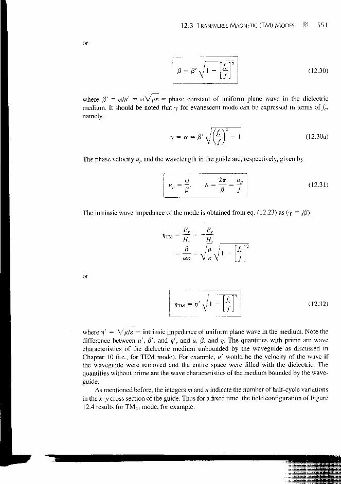
As mentioned before, the integers m and n indicate the number of half-cycle variationsin the x-y cross section of the guide. Thus for a fixed time, the field configuration of Figure12.4 results for TM2, mode, for example.
552 Waveguides
end view
n= 1
E field
H field
Figure 12.4 Field configuration for TM2] mode.
side view
12.4 TRANSVERSE ELECTRIC (TE) MODES
In the TE modes, the electric field is transverse (or normal) to the direction of wave propa-gation. We set Ez = 0 and determine other field components Ex, Ey, Hx, Hy, and Hz fromeqs. (12.12) and (12.15) and the boundary conditions just as we did for the TM modes. Theboundary conditions are obtained from the fact that the tangential components of the elec-tric field must be continuous at the walls of the waveguide; that is,
Exs =
Exs '-
Eys =
Eys =
= 0
= 0
= 0
= 0
From eqs. (12.15) and (12.33), the boundary
dHzs
dy
dHzs
= 0
= 0
at
at
at
at
y = 0
y = b
x = 0
x — a
conditions can be written as
at
at
y-0
y = b
(12.33a)
(12.33b)
(12.33c)
(12.33d)
(12.34a)
(12.34b)dy
dHzs
dx
dHzs
dx
= 0
= 0
at
at
x = 0
x = a
Imposing these boundary conditions on eq. (12.12) yields
(m%x\ fmry\Hzs = Ho cos cos e yz
\ a ) \ b J
(12.34c)
(12.34d)
(12.35)

12.4 TRANSVERSE ELECTRIC (TE) MODES 553
where Ho = BXBT,. Other field components are easily obtained from eqs. (12.35) and(12.15) as
) e
mrx
(12.36a)
(12.36b)
(12.36c)
(12.36d)
where m = 0, 1, 2, 3 , . . .; and n = 0, 1, 2, 3 , . . .; /J and 7 remain as defined for the TMmodes. Again, m and n denote the number of half-cycle variations in the x-y cross sectionof the guide. For TE32 mode, for example, the field configuration is in Figure 12.5. Thecutoff frequency fc, the cutoff wavelength Xc, the phase constant /3, the phase velocity up,and the wavelength X for TE modes are the same as for TM modes [see eqs. (12.28) to(12.31)].
For TE modes, (m, ri) may be (0, 1) or (1, 0) but not (0, 0). Both m and n cannot bezero at the same time because this will force the field components in eq. (12.36) to vanish.This implies that the lowest mode can be TE10 or TE01 depending on the values of a and b,the dimensions of the guide. It is standard practice to have a > b so that I/a2 < 1/b2 in
u' u'eq. (12.28). Thus TEi0 is the lowest mode because /CTE = — < /C.TK = —. This mode is
TE'° la Th°' 2b
top view
E field
//field
Figure 12.5 Field configuration for TE32 mode.

554 i§ Waveguides
called the dominant mode of the waveguide and is of practical importance. The cutoff fre-quency for the TEH) mode is obtained from eq. (12.28) as (m = 1, n — 0)
Jc to 2a(12.37)
and the cutoff wavelength for TE]0 mode is obtained from eq. (12.29) as
Xt,0 = 2a (12.38)
Note that from eq. (12.28) the cutoff frequency for TMn is
u'[a2 + b2]1'2
2ab
which is greater than the cutoff frequency for TE10. Hence, TMU cannot be regarded as thedominant mode.
The dominant mode is the mode with the lowest cutoff frequency (or longest cutoffwavelength).
Also note that any EM wave with frequency / < fCw (or X > XC]0) will not be propagated inthe guide.
The intrinsic impedance for the TE mode is not the same as for TM modes. Fromeq. (12.36), it is evident that (y = jf3)
Ex Ey (J)flr'TE = jry
= ~iTx = T
Ifi 1
or
VTE I
V
12
J
(12.39)
Note from eqs. (12.32) and (12.39) that r)TE and i?TM are purely resistive and they vary withfrequency as shown in Figure 12.6. Also note that
I?TE (12.40)
Important equations for TM and TE modes are listed in Table 12.1 for convenience andquick reference.

12.4 TRANSVERSE ELECTRIC (TE) MODES 555
Figure 12.6 Variation of wave imped-ance with frequency for TE and TMmodes.
TABLE 12.1 Important Equations for TM and TE Modes
TM Modes TE Modes
jP frmc\ fimrx\ . (n%y\ pn (rm\ fmirx\ . (rny\—r I Eo cos sin e 7 £„ = —— I — Ho cos I sin I e '~
h \ a J \ a J \ b J h \ b J \ a ) \ b JExs =
—- \ — )Eo sin | cos -—- ) e 7Z
a J \ b\ / niry
i I cos -—- | e\ a J \ b
Eo sin I sin I — I e 1Z
\ a J \ b )jus
Ezs = 0
Hys = —yh \ a ) \ a ) V b
n*y i e-,,
. = 0
V =
j nnrx \ / rnryHzs = Ho cos cos —-x a V b
V =
where ^ = — + ^ . « ' =
556 Waveguides
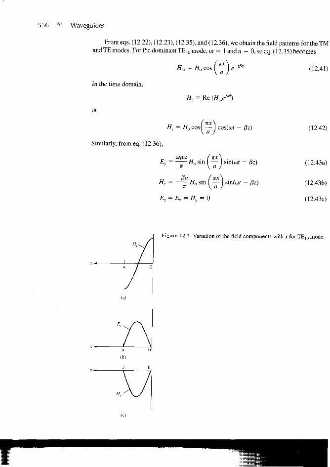
Fromeqs. (12.22), (12.23), (12.35), and (12.36), we obtain the field patterns for the TMand TE modes. For the dominant TE]0 mode, m = landn = 0, so eq. (12.35) becomes
Hzs = Ho cos ( — | e -JPz
In the time domain,
Hz = Re (HzseM)
or
Hz = Ho cosf —
Similarly, from eq. (12.36),
= sin (
Hx = Ho sin ( —\a
- fiz)
(12.41)
(12.42)
(12.43a)
(12.43b)
(12.43c)
Figure 12.7 Variation of the field components with x for TE]0 mode.
(b)
12.4 TRANSVERSE ELECTRIC (TE) MODES 557
Figure 12.8 Field lines for TE10
mode.
+ — Direction ofpropagation
top view
IfMi
'O
\ I^-•--x 1 - * - - N \ \
(c)
E field
//field
Direction ofpropagation
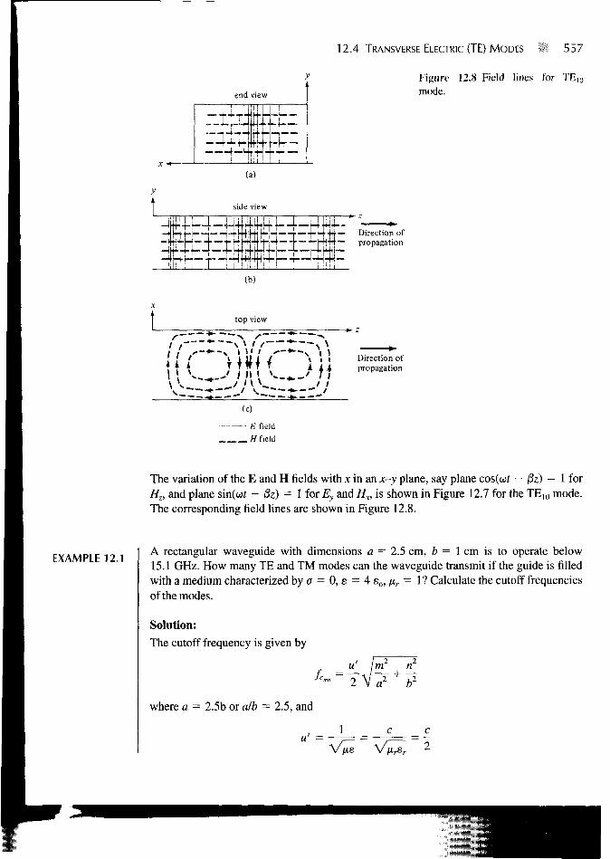
The variation of the E and H fields with x in an x-y plane, say plane cos(wf - |8z) = 1 forHz, and plane sin(of — j8z) = 1 for Ey and Hx, is shown in Figure 12.7 for the TE10 mode.The corresponding field lines are shown in Figure 12.8.
EXAMPLE 12.1A rectangular waveguide with dimensions a = 2.5 cm, b = 1 cm is to operate below15.1 GHz. How many TE and TM modes can the waveguide transmit if the guide is filledwith a medium characterized by a = 0, e = 4 so, /*,. = 1 ? Calculate the cutoff frequenciesof the modes.
Solution:
The cutoff frequency is given by
m2
where a = 2.5b or alb = 2.5, and
u =lie 'V-^r
558 Waveguides
Hence,
c
\~a3 X 108
4(2.5 X 10"Vm2 + 6.25M2
or
fCmn = 3Vm 2 GHz (12.1.1)
We are looking for fCnm < 15.1 GHz. A systematic way of doing this is to fix m or nand increase the other until fCnm is greater than 15.1 GHz. From eq. (12.1.1), it is evidentthat fixing m and increasing n will quickly give us an fCnm that is greater than 15.1 GHz.
ForTE01 mode (m = 0, n = 1), fCm = 3(2.5) = 7.5 GHz
TE02 mode (m = 0,n = 2),/Co2 = 3(5) = 15 GHz
TE03 mode,/Cm = 3(7.5) = 22.5 GHz
Thus for fCmn < 15.1 GHz, the maximum n = 2. We now fix n and increase m until fCmn isgreater than 15.1 GHz.
For TE10 mode (m = 1, n = 0), /C|o = 3 GHz
TE2o mode,/C20 = 6 GHz
TE30 mode,/C3o = 9 GHz
TE40mode,/C40 = 12 GHz
TE50 mode,/Cjo = 1 5 GHz (the same as for TE02)
TE60mode,/C60 = 18 GHz.
that is, for/Cn < 15.1 GHz, the maximum m = 5. Now that we know the maximum m andn, we try other possible combinations in between these maximum values.
F o r T E n , T M n (degenerate modes), fCu = 3\/T25 = 8.078 GHz
TE21, TM2I,/C2i = 3V10.25 = 9.6 GHz
TE3],TM31,/C31 = 3Vl5 .25 = 11.72 GHz
TE41, TM41,/C4] = 3V22.25 = 14.14 GHz
TE12, TM12,/Ci, = 3V26 = 15.3 GHz
Those modes whose cutoff frequencies are less or equal to 15.1 GHz will betransmitted—that is, 11 TE modes and 4 TM modes (all of the above modes except TE i2,TM12, TE60, and TE03). The cutoff frequencies for the 15 modes are illustrated in the linediagram of Figure 12.9.

12.4 TRANSVERSE ELECTRIC (TE) MODES S 559
TE4
TE,, TE30
9'
T E 3 TE41TE50,TE0
12 15• /c(GHz)
TMU TM21 TM31 TM41
Figure 12.9 Cutoff frequencies of rectangular waveguide witha = 2.5b; for Example 12.1.
PRACTICE EXERCISE 12.1
Consider the waveguide of Example 12.1. Calculate the phase constant, phase veloc-ity and wave impedance for TEi0 and TMu modes at the operating frequency of15 GHz.
Answer: For TE10, (3 = 615.6rad/m, u = 1.531 X 10⁸m/s, rjJE = 192.4 0. ForTMn,i3 = 529.4 rad/m, K = 1.78 X 10⁸m/s,rjTM = 158.8 0.
EXAMPLE 12.2Write the general instantaneous field expressions for the TM and TE modes. Deduce thosefor TEOi and TM12 modes.
Solution:
The instantaneous field expressions are obtained from the phasor forms by using
E = Re (EseJ'*) and H = Re (Hse
jo")
Applying these to eqs. (12.22) and (12.23) while replacing y and jfi gives the followingfield components for the TM modes:
sm*= iA ~r j E°cos
j3\nw~\ fmirx\ fmry\= —A—-\EO sm cos —— si
\ a ) \ b J
(nvKx\ . fniryin cm IE7 = En sin
= --£ [T\ Eo sm
" z )
cos

560 • Waveguides
H =y h2 En cosI1 . (niry\ .
sin —— sm(a)t -a J \ b J
(3z)
Hz = 0
Similarly, for the TE modes, eqs. (12.35) and (12.36) become
E= —( mirx\ j mry\
, , Ho cos sin —— sin(ufb \ \ a J \ b J -Pz)
w/x fmir] . (m-wx\ frnry\ .= —r Ho sin cos si
h2 I a \ \ a J \ b J
7 = 0
Ho sin
/3 rn7r]Hy = ~2 [~\ Ho cos
fniry\cos —— sin(wr
b Icos
\ a J \ b I
j sin (-y) sin(.t -2 [ \ Ho cos ^ j
jm-wx\ fniry\H = Ho cos cos cos(co? - pz)
V a J \ b J
For the TE01 mode, we set m = 0, n = 1 to obtain
12
sin
hz= -
$bHy = - — //o sin
7T
iry\Hz = Ho cos I — I cos(cof - /3z)
\b J
For the TM|2 mode, we set m = 1, n = 2 to obtain
cin — cir(3 /TIA / X A . /27ry\ .
Ex = -j I - £o cos — sin — sin(cof - /3z)a / \ b
cos I —— I sir
(TTX\ (2iry\Ez = Eo sin — sin cos(o)fV a J \ b J

12.4 TRANSVERSE ELECTRIC (TE) MODES 561
Hr = — 'o sin I — ) cos ( ^^ ] sin(cof - /3z)
o>e fir\ I\x\ . (2wy\Hy = —r — )EO cos — sin ~~— sm(ut -y h2 \aj \a J V b )
where
PRACTICE EXERCISE 12.2
An air-filled 5- by 2-cm waveguide has
Ezs = 20 sin 40irx sin 50?ry e"-"3" V/m
at 15 GHz.
(a) What mode is being propagated?
(b) Find |8.
(c) Determine EyIEx.
Answer: (a) TM2i, (b) 241.3 rad/m, (c) 1.25 tan 40wx cot 50-ry.
EXAMPLE 12.31 In a rectangular waveguide for which a = 1.5 cm, £ = 0.8 cm, a = 0, fi = JXO, and
e = 4eo,
Hx = 2 sin [ — ) cos sin (T X 10nt - 0z) A/m
Determine
(a) The mode of operation
(b) The cutoff frequency
(c) The phase constant /3
(d) The propagation constant y
(e) The intrinsic wave impedance 77.
Solution:
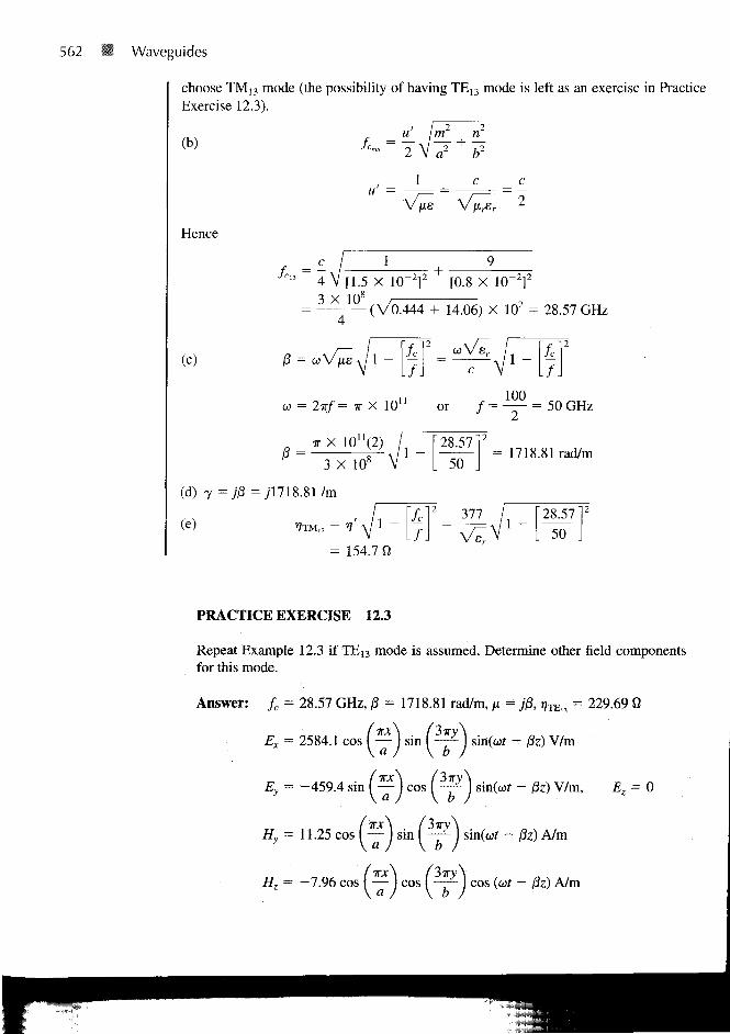
(a) It is evident from the given expression for Hx and the field expressions of the lastexample that m = 1, n = 3; that is, the guide is operating at TMI3 or TE13. Suppose we
562 U Waveguides
choose TM13 mode (the possibility of having TE13 mode is left as an exercise in PracticeExercise 12.3).
(b)
Hence
(c)
fcmn ~ 2 -
u =fiB
fca
14 V [1.5 x icr 2] 2 [0.8 x icr2]r2 ]2
(V0.444 + 14.06) X 102 = 28.57 GHz
L/Jfc
100co = 2TT/ = 7T X 10" or / = = 50 GHz
0 =3 X 10s
(d) y =j0 = yl718.81/m
28.57
50= 1718.81 rad/m
(e) , = V
= 154.7
£12
/377 / _ I 28.5712
50
PRACTICE EXERCISE 12.3
Repeat Example 12.3 if TEn mode is assumed. Determine other field componentsfor this mode.
Answer: fc = 28.57 GHz, 0 = 1718.81 rad/m, ^ = ;/8, IJTE,, = 229.69 fi
£^ = 2584.1 cos ( — ) sin ( — ) sin(w/ - fa) V/m\a J \ b J
Ev = -459.4 sin | — ) cos ( — J sin(cor - fa) V/m,a J \ b J = 0
= 11.25 cos (—) sin( \ / \TTJ: \ / 3;ry \— I sin —— Ia) V b J
sin(a>f - |8z) A/m
= -7.96 cos — cos — - cos (at - fa) A/m\ b J

12.5 WAVE PROPAGATION IN THE GUIDE 563
12.5 WAVE PROPAGATION IN THE GUIDE
Examination of eq. (12.23) or (12.36) shows that the field components all involve theterms sine or cosine of (mi/a)i or (nirlb)y times e~yz. Since
sin 6» = — (eje - e~i6)2/
cos 6 = - (eje + e jB)
(12.44a)
(12.44b)
a wave within the waveguide can be resolved into a combination of plane waves reflectedfrom the waveguide walls. For the TE]0 mode, for example,
(12.45)
c* = ~Hj*-J"
2x _
The first term of eq. (12.45) represents a wave traveling in the positive z-direction at anangle
= tan (12.46)
with the z-axis. The second term of eq. (12.45) represents a wave traveling in the positivez-direction at an angle —6. The field may be depicted as a sum of two plane TEM wavespropagating along zigzag paths between the guide walls at x = 0 and x = a as illustratedin Figure 12.10(a). The decomposition of the TE!0 mode into two plane waves can be ex-tended to any TE and TM mode. When n and m are both different from zero, four planewaves result from the decomposition.
The wave component in the z-direction has a different wavelength from that of theplane waves. This wavelength along the axis of the guide is called the waveguide wave-length and is given by (see Problem 12.13)
X =X'
(12.47)
where X' = u'/f.As a consequence of the zigzag paths, we have three types of velocity: the medium ve-
locity u', the phase velocity up, and the group velocity ug. Figure 12.10(b) illustrates the re-lationship between the three different velocities. The medium velocity u' = 1/V/xe is as
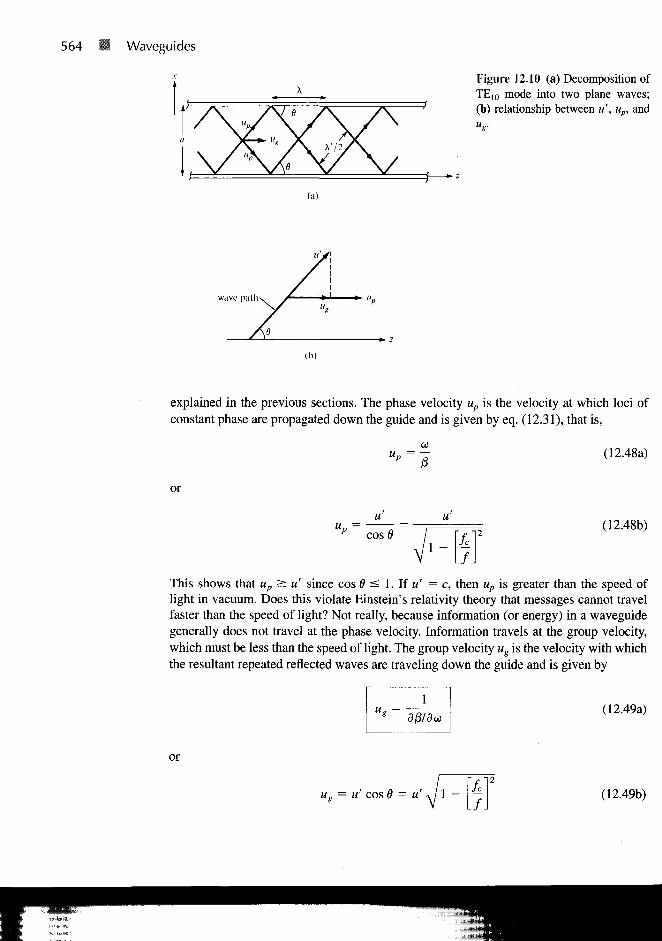
564 Waveguides
Figure 12.10 (a) Decomposition ofTE10 mode into two plane waves;(b) relationship between u', up, and
(a)
wave path
(ID
explained in the previous sections. The phase velocity up is the velocity at which loci ofconstant phase are propagated down the guide and is given by eq. (12.31), that is,
«„ = 7T d2.48a)
or
Up cos e(12.48b)
This shows that up > u' since cos 6 < 1. If u' = c, then up is greater than the speed oflight in vacuum. Does this violate Einstein's relativity theory that messages cannot travelfaster than the speed of light? Not really, because information (or energy) in a waveguidegenerally does not travel at the phase velocity. Information travels at the group velocity,which must be less than the speed of light. The group velocity ug is the velocity with whichthe resultant repeated reflected waves are traveling down the guide and is given by
(12.49a)
or
uo = u' cos 6 = u' (12.49b)

12.6 POWER TRANSMISSION AND ATTENUATION 565
Although the concept of group velocity is fairly complex and is beyond the scope of thischapter, a group velocity is essentially the velocity of propagation of the wave-packet en-velope of a group of frequencies. It is the energy propagation velocity in the guide and isalways less than or equal to u'. From eqs. (12.48) and (12.49), it is evident that
upug = u'2 (12.50)
This relation is similar to eq. (12.40). Hence the variation of up and ug with frequency issimilar to that in Figure 12.6 for r;TE and rjTM.
EXAMPLE 12.4A standard air-filled rectangular waveguide with dimensions a = 8.636 cm, b = 4.318 cmis fed by a 4-GHz carrier from a coaxial cable. Determine if a TE10 mode will be propa-gated. If so, calculate the phase velocity and the group velocity.
Solution:
For the TE10 mode, fc = u' 11a. Since the waveguide is air-filled, u' = c = 3 X 10⁸.Hence,
fc =3 X 10*
= 1.737 GHz2 X 8.636 X 10~2
As / = 4 GHz > fc, the TE10 mode will propagate.
u' 3 X 10⁸
V l - (fjff V l - (1.737/4)2
= 3.33 X 10⁸ m/s16
g
9 X 10j
3.33 X 108= 2.702 X 10⁸ m/s
PRACTICE EXERCISE 12.4
Repeat Example 12.4 for the TM n mode.
Answer: 12.5 X 10⁸ m/s, 7.203 X 10⁷ m/s.
12.6 POWER TRANSMISSION AND ATTENUATION
To determine power flow in the waveguide, we first find the average Poynting vector [fromeq. (10.68)],
(12.51)

566 • Waveguides
In this case, the Poynting vector is along the z-direction so that
1
_ \Ea-\2 + \Eys\
2
2V
(12.52)
where rj = rjTE for TE modes or 77 = »/TM for TM modes. The total average power trans-mitted across the cross section of the waveguide is
— \ at, . J C
(12.53)- dy dx
=0 Jy=0
Of practical importance is the attenuation in a lossy waveguide. In our analysis thusfar, we have assumed lossless waveguides (a = 0, ac — °°) for which a = 0, 7 = j/3.When the dielectric medium is lossy (a # 0) and the guide walls are not perfectly con-ducting (ac =£ 00), there is a continuous loss of power as a wave propagates along theguide. According to eqs. (10.69) and (10.70), the power flow in the guide is of the form
P = P e -2az (12.54)
In order that energy be conserved, the rate of decrease in Pave must equal the time averagepower loss PL per unit length, that is,
P L = -dPa.
dz
or
^ • * fl
In general,
= ac ad
(12.55)
(12.56)
where ac and ad are attenuation constants due to ohmic or conduction losses (ac # 00) anddielectric losses (a ¥= 0), respectively.
To determine ad, recall that we started with eq. (12.1) assuming a lossless dielectricmedium (a = 0). For a lossy dielectric, we need to incorporate the fact that a =£ 0. All ourequations still hold except that 7 = jj3 needs to be modified. This is achieved by replacinge in eq. (12.25) by the complex permittivity of eq. (10.40). Thus, we obtain
mir\ frnr\2 2 (12.57)
12.6 POWER TRANSMISSION AND ATTENUATION 567
where
ec = e' - je" = s - j - (12.58)CO
Substituting eq. (12.58) into eq. (12.57) and squaring both sides of the equation, we obtain
2 27 = ad 2 f t A = l - ^ ) +[~) -Sfiir
Equating real and imaginary parts,
\ a+ \T) (12.59a)
2adf3d = co/xa or ad =
Assuming that ad <£. (3d, azd - j3z
d = -/3J, so eq. (12.59a) gives
a )
(12.59b)
(12.60)
which is the same as (3 in eq. (12.30). Substituting eq. (12.60) into eq. (12.59b) gives
(12.61)
where rj' = V/x/e.The determination of ac for TMmn and TEmn modes is time consuming and tedious. We
shall illustrate the procedure by finding ac for the TE10 mode. For this mode, only Ey, Hx,and Hz exist. Substituting eq. (12.43a) into eq. (12.53) yields
a f b
- dxdy =x=0 Jy= 2ir r)
dy sin — dx
'° ° a (12.62)
* ave
The total power loss per unit length in the walls is
y=o
\y=b + Pi \X=0
=O)(12.63)

568 Waveguides
since the same amount is dissipated in the walls y = 0 and y = b or x = 0 and x = a. Forthe wall y = 0,
TJC j {\Hxs\l+ \Hzs\
z)dxa #2 2
7TJCH2
nsin2 — Hzo cos1 — dx\ (12.64)
£ 1 +7T
where Rs is the real part of the intrinsic impedance t\c of the conducting wall. From eq.(10.56),
1
ar8(12.65)
where 5 is the skin depth. Rs is the skin resistance of the wall; it may be regarded as the re-sistance of 1 m by 5 by 1 m of the conducting material. For the wall x = 0,
C I (\Hzs\z)dy H2
ody
RJbHl(12.66)
Substituting eqs. (12.64) and (12.66) into eq. (12.63) gives
(12.67)
Finally, substituting eqs. (12.62) and (12.67) into eq. (12.55),
?2 2
2ir r/
ar = (12.68a)
It is convenient to express ac. in terms of/ and fc. After some manipulations, we obtain forthe TE10 mode
2RS kL/
(12.68b)
12.7 WAVEGUIDE CURRENT AND MODE EXCITATION 569
By following the same procedure, the attenuation constant for the TEm« modes (n + 0) canbe obtained as
(12.69)r
md for the TMmn
- 'fc
J.
2 (l 1I
modes as
" c TM
OH2
2/?,
2 m
(bid?'fViblaf
, 2
+ n2
m2 +
m2 +
kV
n2 \
\f<}2)[f\)
(12.70)
The total attenuation constant a is obtained by substituting eqs. (12.61) and (12.69) or(12.70) into eq. (12.56).
12.7 WAVEGUIDE CURRENT AND MODE EXCITATION
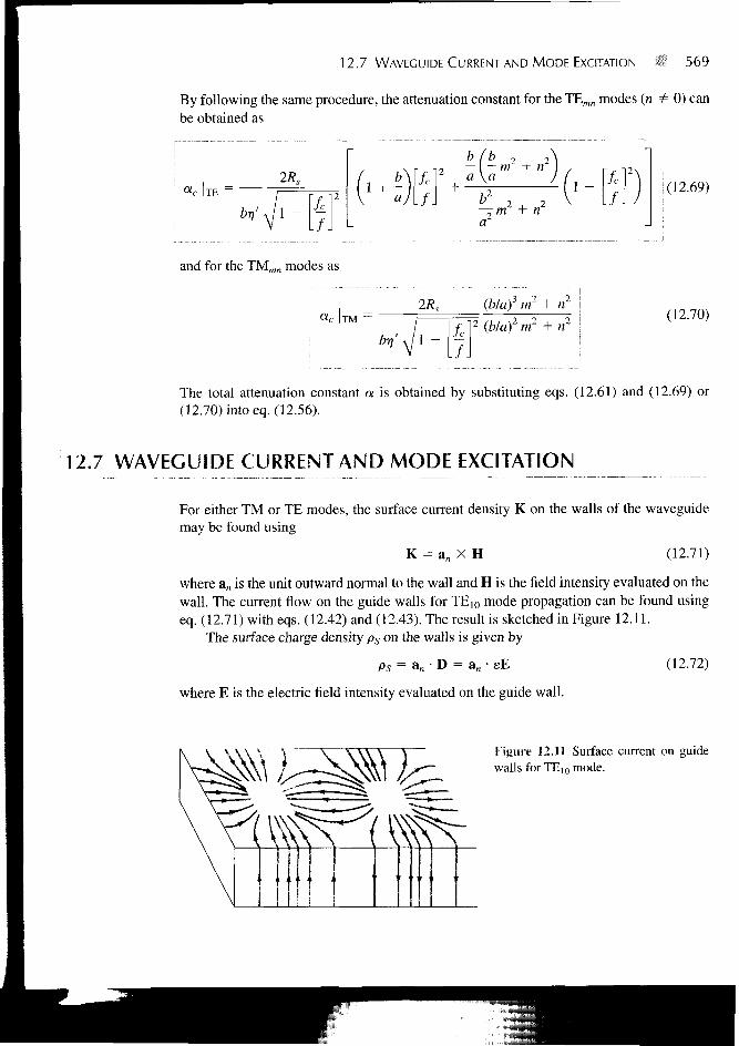
For either TM or TE modes, the surface current density K on the walls of the waveguidemay be found using
K = an X H (12.71)
where an is the unit outward normal to the wall and H is the field intensity evaluated on thewall. The current flow on the guide walls for TE10 mode propagation can be found usingeq. (12.71) with eqs. (12.42) and (12.43). The result is sketched in Figure 12.11.
The surface charge density ps on the walls is given by
ps = an • D = an • eE
where E is the electric field intensity evaluated on the guide wall.
(12.72)
Figure 12.11 Surface current on guidewalls for TE10 mode.
570 Waveguides
?"\J
(a) TE,n mode.
0 a 0
(b)TMM mode.
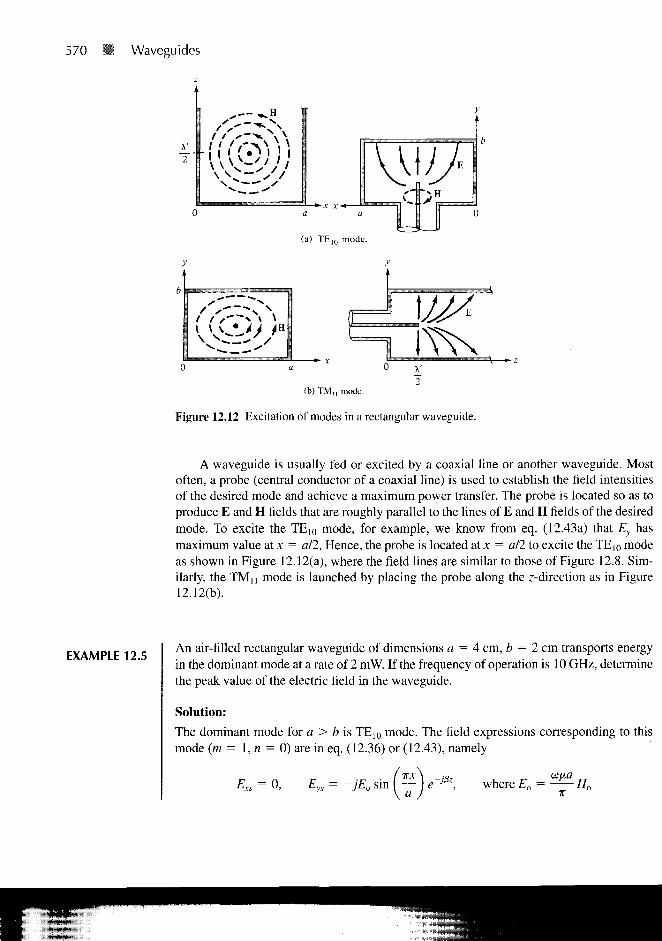
Figure 12.12 Excitation of modes in a rectangular waveguide.
A waveguide is usually fed or excited by a coaxial line or another waveguide. Mostoften, a probe (central conductor of a coaxial line) is used to establish the field intensitiesof the desired mode and achieve a maximum power transfer. The probe is located so as toproduce E and H fields that are roughly parallel to the lines of E and H fields of the desiredmode. To excite the TE10 mode, for example, we know from eq. (12.43a) that Ey hasmaximum value at x = ail. Hence, the probe is located at x = a/2 to excite the TEIO modeas shown in Figure 12.12(a), where the field lines are similar to those of Figure 12.8. Sim-ilarly, the TMii mode is launched by placing the probe along the z-direction as in Figure
EXAMPLE 12.5An air-filled rectangular waveguide of dimensions a = 4 cm, b = 2 cm transports energyin the dominant mode at a rate of 2 mW. If the frequency of operation is 10 GHz, determinethe peak value of the electric field in the waveguide.
Solution:
The dominant mode for a > b is TE10 mode. The field expressions corresponding to thismode (m = 1, n = 0) are in eq. (12.36) or (12.43), namely
Exs = 0, Eys = -jE0 sin ( — where £„ =

12.7 WAVEGUIDE CURRENT AND MODE EXCITATION I I 571
Jc 2a 2(4 X 10~2)
V' 377
/ c
= 406.7
1 -3.75
. / J V L ioFrom eq. (12.53), the average power transmitted is
P = r r \Mave L L 2^
Hence,
dy
4r,
2t, —4(406.7) X 2 X 1Q"3
ab 8 X 10
En = 63.77 V/m
= 4067
PRACTICE EXERCISE 12.5
In Example 12.5, calculate the peak value Ho of the magnetic field in the guide ifa = 2 cm, b = 4 cm while other things remain the same.
Answer: 63.34 mA/m.
EXAMPLE 12.6A copper-plated waveguide (ac = 5.8 X 10⁷ S/m) operating at 4.8 GHz is supposed todeliver a minimum power of 1.2 kW to an antenna. If the guide is filled with polystyrene(a = 10"17 S/m, e = 2.55eo) and its dimensions are a = 4.2 cm, b = 2.6 cm, calculatethe power dissipated in a length 60 cm of the guide in the TE10 mode.
Solution:
Let
Pd = power loss or dissipatedPa = power delivered to the antennaPo = input power to the guide
so that P0 = Pd + Pa
Fromeq. (12.54),
D — D ,,~2<xz
572 Waveguides
Hence,
Pa =-2az
or
Now we need to determine a from
From eq. (12.61),
= Pa(elaz - 1)
a = ad + ac
or,'
Since the loss tangent
10 -17
ue q 10~9
2x X 4.8 X 109 X X 2.5536TT
then
= 1.47 X 10"17 « : 1 (lossless dielectric medium)
= 236.1
= 1.879 X 10⁸m/sBr
2a 2 X 4.2 X 10'
10~17 X 236.1
2.234 GHz
/ _ [2.23412
L 4 .8 Jad = 1.334 X 10~15Np/m
For the TE10 mode, eq. (12.68b) gives
ar =V2
If
0.5 + - kL/J

12.7 WAVEGUIDE CURRENT AND MODE EXCITATION 573
where
Hence
/?. =ac8
= 1.808 X 10~2Q
1 hrfiJ. hrX 4.8 X 109 X 4ir X 10- 7
5.8 X 10⁷
2 X l i
a, =2.6 X1O"2X 236
= 4.218 X 10"3Np/m
/. 1 ^ 1 -
234
Note that ad <§C ac, showing that the loss due to the finite conductivity of the guide wallsis more important than the loss due to the dielectric medium. Thus
a = ad + ac = ac = 4.218 X 10"3 Np/m
and the power dissipated is
= 6.089 WPd = Pa{e^ _ i) = 1.2 x ioV x 4 - 2 1 8 x l o" x a 6 - 1)
PRACTICE EXERCISE 12.6
A brass waveguide (ac = 1.1 X 10⁷ mhos/m) of dimensions a = 4.2 cm, b —1.5 cm is filled with Teflon (er = 2.6, a = 10"15 mhos/m). The operating frequencyis 9 GHz. For the TE10 mode:
(a) Calculate <xd and ac.
(b) What is the loss in decibels in the guide if it is 40 cm long?
Answer: (a) 1.206 X 10~iJ Np/m, 1.744 X 10~zNp/m, (b) 0.0606 dB.
EXAMPLE 12.7Sketch the field lines for the TMn mode. Derive the instantaneous expressions for thesurface current density of this mode.
Solution:
From Example 12.2, we obtain the fields forTMn mode (m = 1, n = 1) as
Ey = Ti i j;) Eo s i n ( ~ ) c o s ( y ) sin(cof - j3z)

574 Waveguides
Ez = Eo sin I — I sin I — I cos(wr - /3z)x a J \ b J
we / TT \ I %x \ iry\Hx = —-j I — £o sin I — I cos I —- sin(wf -
h \bj \a I \ b
we /vr\y = ~tf \a) E°
(TXX
Va
//, = 0
For the electric field lines,
dy E., a firx\ (%y— = - r = 7 tan — cot —cfx £x b \a I \b
For the magnetic field lines,
dy Hy b /TTX\
dx Hx a \ a Jiry \
b JNotice that (Ey/Ex)(Hy/Hx) = — 1, showing that electric and magnetic field lines are mutu-ally orthogonal. This should also be observed in Figure 12.13 where the field lines aresketched.
The surface current density on the walls of the waveguide is given by
K = an X H = a* X (Hx, Hy, 0)
At x = 0, an = ax, K = Hy(0, y, z, t) az, that is,
we fir
At x = a, an = -a x , K = -Hy(a, y, z, i) az
or
Tr we (ir
1? \a
Figure 12.13 Field lines for TMU mode; forExample 12.7.
E field
H field

12.8 WAVEGUIDE RESONATORS 575
At y = 0, an = ay, K = -Hx(x, 0, z, t) az
or
Aty = b,an = -ay, K = Hx(x, b, z, t) az
or
COS / 7T \ / TTX ,K = — I — ) Eo sin — sm(atf - j3z) az
h \bj \ a
- I3z) az
PRACTICE EXERCISE 12.7
Sketch the field lines for the TE n mode.
Answer: See Figure 12.14. The strength of the field at any point is indicated by thedensity of the lines; the field is strongest (or weakest) where the lines areclosest together (or farthest apart).
12.8 WAVEGUIDE RESONATORS
Resonators are primarily used for energy storage. At high frequencies (100 MHz andabove) the RLC circuit elements are inefficient when used as resonators because the di-mensions of the circuits are comparable with the operating wavelength, and consequently,unwanted radiation takes place. Therefore, at high frequencies the RLC resonant circuits
end view side view
U J©i ©^
©| !©[
E field//field
top view
Figure 12.14 For Practice Exercise 12.7; for TEn mode.
576 Waveguides
are replaced by electromagnetic cavity resonators. Such resonator cavities are used in kly-stron tubes, bandpass filters, and wave meters. The microwave oven essentially consists ofa power supply, a waveguide feed, and an oven cavity.
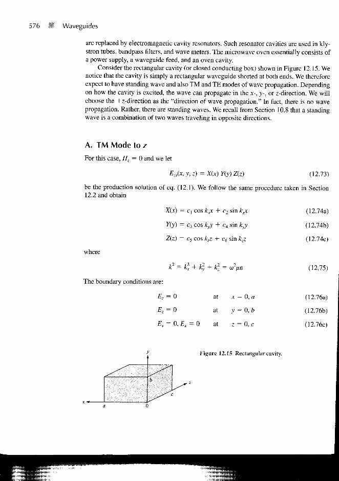
Consider the rectangular cavity (or closed conducting box) shown in Figure 12.15. Wenotice that the cavity is simply a rectangular waveguide shorted at both ends. We thereforeexpect to have standing wave and also TM and TE modes of wave propagation. Dependingon how the cavity is excited, the wave can propagate in the x-, y-, or z-direction. We willchoose the +z-direction as the "direction of wave propagation." In fact, there is no wavepropagation. Rather, there are standing waves. We recall from Section 10.8 that a standingwave is a combination of two waves traveling in opposite directions.
A. TM Mode to z
For this case, Hz = 0 and we let
EJx, y, z) = X(x) Y(y) Z(z) (12.73)
be the production solution of eq. (12.1). We follow the same procedure taken in Section12.2 and obtain
X(x) = C\ cos kjX + c2 sin kpc
Y(y) = c3 cos kyy + c4 sin kyy
Z(z) = c5 cos kzz + c6 sin kzz,
where
k2 = k2x + k], + k] = u2ixe
The boundary conditions are:
£z = 0 at x = 0, a
Ez = 0 at >' = 0 ,6
Ey = 0,Ex = 0 at z = 0, c
(12.74a)
(12.74b)
(12.74c)
(12.75)
(12.76a)
(12.76b)
(12.76c)
Figure 12.15 Rectangular cavity.

12.8 WAVEGUIDE RESONATORS • 577
As shown in Section 12.3, the conditions in eqs. (12.7a, b) are satisfied whencx = 0 = c3 and
nvKa y b
(12.77)
where m = 1, 2, 3, . . ., n = 1, 2, 3, . . . .To invoke the conditions in eq. (12.76c), wenotice that eq. (12.14) (with Hzs = 0) yields
d2Exs d2Ezs
dz dz
Similarly, combining eqs. (12.13a) and (12.13d) (with Hzs = 0) results in
-ycoe ys -
From eqs. (12.78) and (12.79), it is evident that eq. (12.76c) is satisfied if
— - = 0 at z = 0, cdz
This implies that c6 = 0 and sin kzc = 0 = sin pir. Hence,
(12.78)
(12.79)
(12.80)
(12.81)
where p = 0, 1, 2, 3 , . . . . Substituting eqs. (12.77) and (12.81) into eq. (12.74) yields
(12.82)
where Eo = c2c4c5. Other field components are obtained from eqs. (12.82) and (12.13).The phase constant /3 is obtained from eqs. (12.75), (12.77), and (12.81) as
(12.83)
Since /32 = co2/i£, from eq. (12.83), we obtain the resonant frequency fr
2irfr = ur =fie
or
ufr ^
/r i/ w[a\
2 r 12
" 1 Ir "
r (12.84)
578 • Waveguides
The corresponding resonant wavelength is
u'
" fr llmVU rJ
2
In
L ^f +1 UJ
9 (12.85)
From eq. (12.84), we notice that the lowest-order TM mode is TM110-
B. TE Mode to z
In this case, Ez = 0 and
Hzs = (bt cos sin 3 cos kyy + b4 sin kyy)(^5 cos kzz + sin kzz)
The boundary conditions in eq. (12.76c) combined with eq. (12.13) yields
at z = 0, cHzs =
dx
dy
= 0 at x = 0, a
= 0 at = 0,b
(12.86)
(12.87a)
(12.87b)
(12.87c)
Imposing the conditions in eq. (12.87) on eq. (12.86) in the same manner as for TM modeto z leads to
(12.88)
where m = 0, 1, 2, 3, . . ., n = 0, 1, 2, 3, . . ., and p = 1, 2, 3, . . . . Other field com-ponents can be obtained from eqs. (12.13) and (12.88). The resonant frequency is thesame as that of eq. (12.84) except that m or n (but not both at the same time) can bezero for TE modes. The reason why m and n cannot be zero at the same time is that thefield components will be zero if they are zero. The mode that has the lowest resonantfrequency for a given cavity size (a, b, c) is the dominant mode. If a > b < c, it impliesthat I/a < \lb > lie and hence the dominant mode is TE101. Note that for a > b < c, theresonant frequency of TMU0 mode is higher than that for TE101 mode; hence, TE101 isdominant. When different modes have the same resonant frequency, we say that themodes are degenerate; one mode will dominate others depending on how the cavity isexcited.
A practical resonant cavity has walls with finite conductivity ac and is, therefore,capable of losing stored energy. The quality factor Q is a means of determining the loss.
12.8 WAVEGUIDE RESONATORS 579
The qiialitx factor is also a measure of I he bandwidth ol' the cavity resonator.
It may be defined as
Time average energy storedEnergy loss per cycle of oscillationW W
(12.89)
where T = 1// = the period of oscillation, PL is the time average power loss in the cavity,and W is the total time average energy stored in electric and magnetic fields in the cavity.Q is usually very high for a cavity resonator compared with that for an RLC resonantcircuit. By following a procedure similar to that used in deriving ac in Section 12.6, it canbe shown that the quality factor for the dominant TE]01 is given by3
GTE 1 0 1 =5[2b(a3
(a2
+ c
+3)
c2)abc
+ acia fc!)](12.90)
where 5 = is the skin depth of the cavity walls.
EXAMPLE 12.8An air-filled resonant cavity with dimensions a = 5 cm, b = 4 cm, and c = 10 cm ismade of copper (oc = 5.8 X 10⁷ mhos/m). Find
(a) The five lowest order modes
(b) The quality factor for TE1Oi mode
Solution:
(a) The resonant frequency is given by
m
where
u' = = c
3For the proof, see S. V. Marshall and G. G. Skitek, Electromagnetic Concepts and Applications, 3rded. Englewood Cliffs, NJ: Prentice-Hall, 1990, pp. 440-442.

580 S Waveguides
Hence
3 X l(f m5 X 10" 4 X 10- 2 10 X 10 - 2
= 15V0.04m2 + 0.0625«2 + 0.01/?2 GHz
Since c > a > b or 1/c < I/a < 1/&, the lowest order mode is TE101. Notice thatTMioi and TE1Oo do not exist because m = 1,2, 3, . . ., n = 1,2, 3, . . ., andp = 0, 1, 2, 3, . . . for the TM modes, and m = 0, 1, 2, . . ., n = 0, 1, 2, . . ., andp = 1,2,3,. . . for the TE modes. The resonant frequency for the TE1Oi mode is
frm = 15V0.04 + 0 + 0.01 = 3.335 GHz
The next higher mode is TE011 (TM011 does not exist), with
fron = 15V0 + 0.0625 + 0.01 = 4.04 GHz
The next mode is TE102 (TM!02 does not exist), with
frim = 15V0.04 + 0 + 0.04 = 4.243 GHz
The next mode is TM110 (TE110 does not exist), with
fruo = 15V0.04 + 0.0625 + 0 = 4.8 GHz
The next two modes are TE i n and TM n ] (degenerate modes), with
frni = 15V0.04 + 0.0625 + 0.01 = 5.031 GHz
The next mode is TM103 with
frm = 15V0.04 + 0 + 0.09 = 5.408 GHz
Thus the five lowest order modes in ascending order are
TE101 (3.35 GHz)
TEon (4.04 GHz)TE102 (4.243 GHz)TMU 0 (4.8 GHz)T E i , , o r T M i n (5.031 GHz)
(b) The quality factor for TE]01 is given by
2TEI01 -(a2 c2) abc
S[2b(a c3) ac(a2 c2)]
(25 + 100) 200 X 10~2
5[8(125 + 1000) + 50(25 + 100)]
616 61
VV(3.35 X 10⁹) 4TT X 10"7 (5.8 X 10⁷)
61= 14,358

SUMMARY 581
PRACTICE EXERCISE 12.8
If the resonant cavity of Example 12.8 is filled with a lossless material (/xr = 1,er - 3), find the resonant frequency fr and the quality factor for TE101 mode.
Answer: 1.936 GHz, 1.093 X 10⁴
SUMMARY 1. Waveguides are structures used in guiding EM waves at high frequencies. Assuming alossless rectangular waveguide (ac — o°, a — 0), we apply Maxwell's equations in ana-lyzing EM wave propagation through the guide. The resulting partial differential equa-tion is solved using the method of separation of variables. On applying the boundaryconditions on the walls of the guide, the basic formulas for the guide are obtained fordifferent modes of operation.
2. Two modes of propagation (or field patterns) are the TMmn and TEmn where m and n arepositive integers. For TM modes, m = 1, 2, 3, . . ., and n = 1, 2, 3, . . . and for TEmodes, m = 0, 1, 2, . . ., and n = 0, 1, 2, . . .,n = m¥z0.
3. Each mode of propagation has associated propagation constant and cutoff frequency.The propagation constant y = a + jfl does not only depend on the constitutive pa-rameters (e, /x, a) of the medium as in the case of plane waves in an unbounded space,it also depends on the cross-sectional dimensions (a, b) of the guide. The cutoff fre-quency is the frequency at which y changes from being purely real (attenuation) topurely imaginary (propagation). The dominant mode of operation is the lowest modepossible. It is the mode with the lowest cutoff frequency. If a > b, the dominant modeis TE10.
4. The basic equations for calculating the cutoff frequency fc, phase constant 13, and phasevelocity u are summarized in Table 12.1. Formulas for calculating the attenuation con-stants due to lossy dielectric medium and imperfectly conducting walls are also pro-vided.
5. The group velocity (or velocity of energy flow) ug is related to the phase velocity up ofthe wave propagation by
upug = u'2
where u' = 1/v/xs is the medium velocity—i.e., the velocity of the wave in the di-electric medium unbounded by the guide. Although up is greater than u', up does notexceed u'.
6. The mode of operation for a given waveguide is dictated by the method of exci-tation.
7. A waveguide resonant cavity is used for energy storage at high frequencies. It is nothingbut a waveguide shorted at both ends. Hence its analysis is similar to that of a wave-guide. The resonant frequency for both the TE and TM modes to z is given by
m

582 Waveguides
For TM modes, m = 1, 2, 3, . . ., n = 1, 2, 3, . . ., and p = 0, 1, 2, 3, . . ., and forTE modes, m = 0,1,2,3,. . ., n = 0, 1, 2, 3 , . . ., and p = 1, 2, 3 , . . .,m = n ^ 0.If a > b < c, the dominant mode (one with the lowest resonant frequency) is TE1Oi-
8. The quality factor, a measure of the energy loss in the cavity, is given by
2 = "-?
12.1 At microwave frequencies, we prefer waveguides to transmission lines for transportingEM energy because of all the following except that
(a) Losses in transmission lines are prohibitively large.
(b) Waveguides have larger bandwidths and lower signal attenuation.
(c) Transmission lines are larger in size than waveguides.
(d) Transmission lines support only TEM mode.
12.2 An evanscent mode occurs when
(a) A wave is attenuated rather than propagated.
(b) The propagation constant is purely imaginary.
(c) m = 0 = n so that all field components vanish.
(d) The wave frequency is the same as the cutoff frequency.
12.3 The dominant mode for rectangular waveguides is
(a) TE,,
(b) TM n
(c) TE1Oi
(d) TE10
12.4 The TM10 mode can exist in a rectangular waveguide.
(a) True
(b) False
12.5 For TE30 mode, which of the following field components exist?
(a) Ex
(b) Ey
(c) Ez
(d) Hx
(e) Hv

PROBLEMS 583
12.6 If in a rectangular waveguide for which a = 2b, the cutoff frequency for TE02 mode is12 GHz, the cutoff frequency for TMH mode is
(a) 3 GHz(b) 3 \ /5GHz(c) 12 GHz
(d) 6 \A GHz(e) None of the above
12.7 If a tunnel is 4 by 7 m in cross section, a car in the tunnel will not receive an AM radiosignal (e.g.,/= 10 MHz).
(a) True
(b) False
12.8 When the electric field is at its maximum value, the magnetic energy of a cavity is
(a) At its maximum value(b) At V 2 of its maximum value
(c) At —-p of its maximum valueV 2
(d) At 1/2 of its maximum value
(e) Zero
12.9 Which of these modes does not exist in a rectangular resonant cavity?
(a) TE110
(b) TEQH
(c) TM110
(d) TMm
12.10 How many degenerate dominant modes exist in a rectangular resonant cavity for whicha = b = c?
(a) 0(b) 2
(c) 3
(d) 5(e) oo
Answers: 12.1c, 12.2a, 12.3d, 12.4b, 12.5b,d, 12.6b, 12.7a, 12.8e, 12.9a, 12.10c.
PROBLEMS I ^** ^ ^ n o w m a t a rectangular waveguide does not support TM10 and TM01 modes.(b) Explain the difference between TEmn and TMmn modes.

584 Waveguides
12.2 A 2-cm by 3-cm waveguide is filled with a dielectric material with er = 4. If the wave-guide operates at 20 GHz with TMU mode, find: (a) cutoff frequency, (b) the phase con-stant, (c) the phase velocity.
12.3 A 1-cm X 2-cm waveguide is filled with deionized water with er = 81. If the operatingfrequency is 4.5 GHz, determine: (a) all possible propagating modes and their cutoff fre-quencies, (b) the intrinsic impedance of the highest mode, (c) the group velocity of thelowest mode.
12.4 Design a rectangular waveguide with an aspect ratio of 3 to 1 for use in the k band(18-26.5 GHz). Assume that the guide is air filled.
12.5 A tunnel is modeled as an air-filled metallic rectangular waveguide with dimensionsa = 8 m and b = 16 m. Determine whether the tunnel will pass: (a) a 1.5-MHz AMbroadcast signal, (b) a 120-MHz FM broadcast signal.
12.6 In an air-filled rectangular waveguide, the cutoff frequency of a TE10 mode is 5 GHz,whereas that of TEOi mode is 12 GHz. Calculate
(a) The dimensions of the guide
(b) The cutoff frequencies of the next three higher TE modes
(c) The cutoff frequency for TEn mode if the guide is filled with a lossless material
having er = 2.25 and (ir=\.
12.7 An air-filled hollow rectangular waveguide is 150 m long and is capped at the end witha metal plate. If a short pulse of frequency 7.2 GHz is introduced into the input end of theguide, how long does it take the pulse to return to the input end? Assume that the cutofffrequency of the guide is 6.5 GHz.
12.8 Calculate the dimensions of an air-filled rectangular waveguide for which the cutoff fre-quencies for TM n and TE03 modes are both equal to 12 GHz. At 8 GHz, determinewhether the dominant mode will propagate or evanesce in the waveguide.
12.9 An air-filled rectangular waveguide has cross-sectional dimensions a = 6 cm andb = 3 cm. Given that
E, = 5 sin (—) sin (-*A cos (1012f - 0z) V/mV a ) V b )
calculate the intrinsic impedance of this mode and the average power flow in theguide.
12.10 In an air-filled rectangular waveguide, a TE mode operating at 6 GHz has
Ey = 5 sm(2irx/a) cos(wy/b) sm(a>t — 12z) V/m
Determine: (a) the mode of operation, (b) the cutoff frequency, (c) the intrinsic imped-ance, (d) Hx.

PROBLEMS 585
12.11 In an air-filled rectangular waveguide with a = 2.286 cm and b = 1.016 cm, they-component of the TE mode is given by
Ey = sin(27rx/a) sin(107r X 1010r - j3z) V/m
find: (a) the operating mode, (b) the propagation constant 7, (c) the intrinsic impedance
V-
12.12 For the TM,, mode, derive a formula for the average power transmitted down the guide.
12.13 (a) Show that for a rectangular waveguide.
" ' x =X'
1 -
(b) For an air-filled waveguide with a = 2b = 2.5 cm operating at 20 GHz, calculateup and X for TE n and TE2i modes.
12.14 A 1-cm X 3-cm rectangular air-filled waveguide operates in the TE|2 mode at a fre-quency that is 20% higher than the cutoff frequency. Determine: (a) the operating fre-quency, (b) the phase and group velocities.
12.15 A microwave transmitter is connected by an air-filled waveguide of cross section2.5 cm X 1 cm to an antenna. For transmission at 11 GHz, find the ratio of (a) the phasevelocity to the medium velocity, and (b) the group velocity to the medium velocity.
12.16 A rectangular waveguide is filled with polyethylene (s = 2.25eo) and operates at 24GHz. If the cutoff frequency of a certain TE mode is 16 GHz, find the group velocity andintrinsic impedance of the mode.
12.17 A rectangular waveguide with cross sections shown in Figure 12.16 has dielectric dis-continuity. Calculate the standing wave ratio if the guide operates at 8 GHz in the domi-nant mode.
*12.18 Analysis of circular waveguide requires solution of the scalar Helmholtz equation incylindrical coordinates, namely
V2EZS + k2Ezs = 0
2.5 cm
5 cm
Figure 12.16 For Problem 12.17.
fio, so fio, 2.25so
586 Waveguides
or
1 d f dEzs\ 1 d2Ea d2Ezs 2
p dp V dp / p 30 3z
By assuming the product solution
Ezs(p, </>, z) = R(p) $(<t>) Z(z)
show that the separated equations are:
Z" - k\ Z = 0
$" + *i $ = o
where
" + pR' + (A:2 p2 - kl) R = 0
t2 = /t2 + *2
12.19 For TE01 mode,
£xs = Y Ho sin(iry/b)e 7 \ Eys =
Find and Pa
12.20 A 1-cm X 2-cm waveguide is made of copper (ac = 5.8 X 10⁷ S/m) and filled with adielectric material for which e = 2.6eo, \i = po, ad = 1CT4 S/m. If the guide operatesat 9 GHz, evaluate ac and ad for (a) TE10, and (b) TMU.
12.21 A 4-cm-square waveguide is filled with a dielectric with complex permittivity ec =16eo(l — 7IO"4) and is excited with the TM2i mode. If the waveguide operates at 10%above the cutoff frequency, calculate attenuation ad. How far can the wave travel downthe guide before its magnitude is reduced by 20%?
12.22 If the walls of the square waveguide in the previous problem are made of brass (ac =1.5 X 10 S/m), find ac and the distance over which the wave is attenuated by 30%.
12.23 A rectangular waveguide with a = 2b = 4.8 cm is filled with teflon with er = 2 . 1 1 andloss tangent of 3 X 10~4. Assume that the walls of the waveguide are coated with gold(<7C = 4.1 X 10⁷ S/m) and that a TE10 wave at 4 GHz propagates down the waveguide,find: (a) ad, (b) ctc.
*12.24 A rectangular brass (ac = 1.37 X 10⁷ S/m) waveguide with dimensions a = 2.25 cmand b = 1.5 cm operates in the dominant mode at frequency 5 GHz. If the waveguide isfilled with teflon (p,r = 1, er = 2.11, a — 0), determine: (a) the cutoff frequency for thedominant mode, (b) the attenuation constant due to the loss in the guide walls.
*12.25 For a square waveguide, show that attenuation ac. is minimum for TE1() mode when/ = 2 . 9 6 2 / c .
PROBLEMS 587
12.26 The attenuation constant of a TM mode is given by
At what frequency will a be maximum?
*12.27 Show that for TE mode to z in a rectangular cavity,
jwix.(mir\ . fmirx\ Iniry\ . /pirzEys = — - A )HO sin cos —— sin
h• \ a J \ a ) \ b J \ c
Find Hxs.
* 12.28 For a rectangular cavity, show that
( pirzc o s
for TM mode to z. Determine Eys.
12.29 In a rectangular resonant cavity, which mode is dominant when
(a) a < b < c
(b) a > b > c
(c) a = c> b
12.30 For an air-filled rectangular cavity with dimensions a = 3 cm, b = 2 cm, c = 4 cm,determine the resonant frequencies for the following modes: TE o n , TE101, TMno, andTM1U. List the resonant frequencies in ascending order.
12.31 A rectangular cavity resonator has dimensions a = 3 cm, b = 6 cm, and c = 9 cm. If itis filled with polyethylene (e = 2.5e0), find the resonant frequencies of the first fivelowest-order modes.
12.32 An air-filled cubical cavity operates at a resonant frequency of 2 GHz when excited atthe TE1Oi mode. Determine the dimensions of the cavity.
12.33 An air-filled cubical cavity of size 3.2 cm is made of brass (<jc = 1.37 X 10⁷ S/m). Cal-culate: (a) the resonant frequency of the TE101 mode, (b) the quality factor at that mode.
12.34 Design an air-filled cubical cavity to have its dominant resonant frequency at 3 GHz.
12.35 An air-filled cubical cavity of size 10 cm has
E = 200 sin 30TTX sin 30iry cos 6 X l09r a, V/m
Find H.

Chapter 13
ANTENNAS
The Ten Commandments of Success1. Hard Work: Hard work is the best investment a man can make.2. Study Hard: Knowledge enables a man to work more intelligently and effec-
tively.3. Have Initiative: Ruts often deepen into graves.4. Love Your Work: Then you will find pleasure in mastering it.5. Be Exact: Slipshod methods bring slipshod results.6. Have the Spirit of Conquest: Thus you can successfully battle and overcome
difficulties.7. Cultivate Personality: Personality is to a man what perfume is to the flower.8. Help and Share with Others: The real test of business greatness lies in giving
opportunity to others.9. Be Democratic: Unless you feel right toward your fellow men, you can never
be a successful leader of men.10. In all Things Do Your Best: The man who has done his best has done every-
thing. The man who has done less than his best has done nothing.
—CHARLES M. SCHWAB
13.1 INTRODUCTION
Up until now, we have not asked ourselves how EM waves are produced. Recall that elec-tric charges are the sources of EM fields. If the sources are time varying, EM waves prop-agate away from the sources and radiation is said to have taken place. Radiation may bethought of as the process of transmitting electric energy. The radiation or launching of thewaves into space is efficiently accomplished with the aid of conducting or dielectric struc-tures called antennas. Theoretically, any structure can radiate EM waves but not all struc-tures can serve as efficient radiation mechanisms.
An antenna may also be viewed as a transducer used in matching the transmission lineor waveguide (used in guiding the wave to be launched) to the surrounding medium or viceversa. Figure 13.1 shows how an antenna is used to accomplish a match between the lineor guide and the medium. The antenna is needed for two main reasons: efficient radiationand matching wave impedances in order to minimize reflection. The antenna uses voltageand current from the transmission line (or the EM fields from the waveguide) to launch anEM wave into the medium. An antenna may be used for either transmitting or receivingEM energy.
588

13.1 INTRODUCTION 589
EM wave
Generator Transmission line
Antenna
Surrounding medium
Figure 13.1 Antenna as a matching device between the guiding struc-ture and the surrounding medium.
Typical antennas are illustrated in Figure 13.2. The dipole antenna in Figure 13.2(a)consists of two straight wires lying along the same axis. The loop antenna in Figure 13.2(b)consists of one or more turns of wire. The helical antenna in Figure 13.2(c) consists of awire in the form of a helix backed by a ground plane. Antennas in Figure 13.2(a-c) arecalled wire antennas; they are used in automobiles, buildings, aircraft, ships, and so on.The horn antenna in Figure 13.2(d), an example of an aperture antenna, is a taperedsection of waveguide providing a transition between a waveguide and the surroundings.Since it is conveniently flush mounted, it is useful in various applications such as aircraft.The parabolic dish reflector in Figure 13.2(e) utilizes the fact that EM waves are reflectedby a conducting sheet. When used as a transmitting antenna, a feed antenna such as adipole or horn, is placed at the focal point. The radiation from the source is reflected by thedish (acting like a mirror) and a parallel beam results. Parabolic dish antennas are used incommunications, radar, and astronomy.
The phenomenon of radiation is rather complicated, so we have intentionally delayedits discussion until this chapter. We will not attempt a broad coverage of antenna theory;our discussion will be limited to the basic types of antennas such as the Hertzian dipole, thehalf-wave dipole, the quarter-wave monopole, and the small loop. For each of these types,we will determine the radiation fields by taking the following steps:
1. Select an appropriate coordinate system and determine the magnetic vector poten-tial A.
2. Find H from B = /tH = V X A.
3. Determine E from V X H = e or E = i;H X as assuming a lossless mediumdt
(a = 0).4. Find the far field and determine the time-average power radiated using
dS, where ve = | Re (E, X H*)
Note that Pnd throughout this chapter is the same as Pme in eq. (10.70).

590 Antennas
(a) dipole (b) loop
(c) helix
(d) pyramidal horn
Radiatingdipole
Reflector
(e) parabolic dish reflector
Figure 13.2 Typical antennas.
13.2 HERTZIAN DIPOLE
By a Hertzian dipole, we mean an infinitesimal current element / dl. Although such acurrent element does not exist in real life, it serves as a building block from which the fieldof a practical antenna can be calculated by integration.
Consider the Hertzian dipole shown in Figure 13.3. We assume that it is located at theorigin of a coordinate system and that it carries a uniform current (constant throughout thedipole), I = Io cos cot. From eq. (9.54), the retarded magnetic vector potential at the fieldpoint P, due to the dipole, is given by
A =A-wr
(13.1)
13.2 HERTZIAN DIPOLE 591
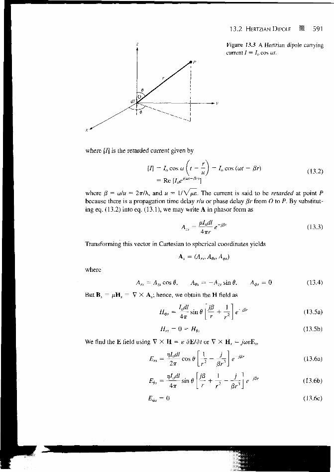
Figure 13.3 A Hertzian dipole carryingcurrent I = Io cos cot.
where [/] is the retarded current given by
[/] = Io cos a) ( t ) = Io cos {bit - (3r)u J
(13.2)= Re [Ioe
j(M-M]
where (3 = to/w = 2TT/A, and u = 1/V/xe. The current is said to be retarded at point Pbecause there is a propagation time delay rlu or phase delay /3r from O to P. By substitut-ing eq. (13.2) into eq. (13.1), we may write A in phasor form as
(13.3)Azs A e
Transforming this vector in Cartesian to spherical coordinates yields
A, = (Ars, A6s, A^)
where
A n . = A z s cos 8, Affs = —Azs sin 6,
But B, = ^H, = V X As; hence, we obtain the H field as
= 0
IodlH^ = —— sin 0 — + - r e
j!3
** 4x lr r-
Hrs = 0 = //Ss
We find the E field using V X H = e dWdt or V X Hs = jueEs,
_ : , - u — ^ ^ fl ! _ - j__ | ^ - 7 / 3 r
E^ = 0
r r
(13.4)
(13.5a)
(13.5b)
(13.6a)
(13.6b)
(13.6c)

592 Hi Antennas
where
V =
A close observation of the field equations in eqs. (13.5) and (13.6) reveals that wehave terms varying as 1/r3, 1/r2, and 1/r. The 1/r3 term is called the electrostatic field sinceit corresponds to the field of an electric dipole [see eq. (4.82)]. This term dominates overother terms in a region very close to the Hertzian dipole. The 1/r term is called the induc-tive field, and it is predictable from the Biot-Savart law [see eq. 7.3)]. The term is impor-tant only at near field, that is, at distances close to the current element. The 1/r term iscalled the far field or radiation field because it is the only term that remains at the far zone,that is, at a point very far from the current element. Here, we are mainly concerned with thefar field or radiation zone (j3r 5> 1 or 2irr S> X), where the terms in 1/r3 and 1/r2 can beneglected in favor of the 1/r term. Thus at far field,
4-irrsin 6 e - V
- Ers - = 0
(I3.7a)
(I3.7b)
Note from eq. (13.7a) that the radiation terms of H$s and E9s are in time phase and orthog-onal just as the fields of a uniform plane wave. Also note that near-zone and far-zone fieldsare determined respectively to be the inequalities /3r <$C I and f3r > I. More specifically,we define the boundary between the near and the far zones by the value of r given by
2d2
r = (13.8)
where d is the largest dimension of the antenna.The time-average power density is obtained as
12Pave = ~ Re (Es X H*) = ^ Re (E6s H% ar)
(13.9)
Substituting eq. (13.7) into eq. (13.9) yields the time-average radiated power as
dS
<t>=o Je=o
3 2 T T 2
327r2r2sin2 6 r2 sin 6 dd d<j> (13.10)
2TT sin* 6 dO

13.2 HERTZIAN DIPOLE • 593
But
sin' 6d6 = \ (1 - cosz 0) d(-cos 9)
cos30— cos i
and 02 = 4TT2/X2. Hence eq. (13.10) becomes
^rad ~dl
3 L X.
If free space is the medium of propagation, rj = 120TT and
(13.11a)
(13.11b)
This power is equivalent to the power dissipated in a fictitious resistance /?rad by currentI = Io cos cot that is
~rad * rms " rad
or
1(13.12)
where /rms is the root-mean-square value of/. From eqs. (13.11) and (13.12), we obtain
OPr» z ' * rad /1 o 11 \
rad = -ZV (13.13a)
or
(13.13b)
The resistance Rmd is a characteristic property of the Hertzian dipole antenna and is calledits radiation resistance. From eqs. (13.12) and (13.13), we observe that it requires anten-nas with large radiation resistances to deliver large amounts of power to space. Forexample, if dl = X/20, Rrad = 2 U, which is small in that it can deliver relatively smallamounts of power. It should be noted that /?rad in eq. (13.13b) is for a Hertzian dipole infree space. If the dipole is in a different, lossless medium, rj = V/x/e is substituted ineq. (13.11a) and /?rad is determined using eq. (13.13a).
Note that the Hertzian dipole is assumed to be infinitesimally small (& dl <S^ 1 ordl ^ X/10). Consequently, its radiation resistance is very small and it is in practice difficultto match it with a real transmission line. We have also assumed that the dipole has a
594 Antennas
uniform current; this requires that the current be nonzero at the end points of the dipole.This is practically impossible because the surrounding medium is not conducting.However, our analysis will serve as a useful, valid approximation for an antenna withdl s X/10. A more practical (and perhaps the most important) antenna is the half-wavedipole considered in the next section.
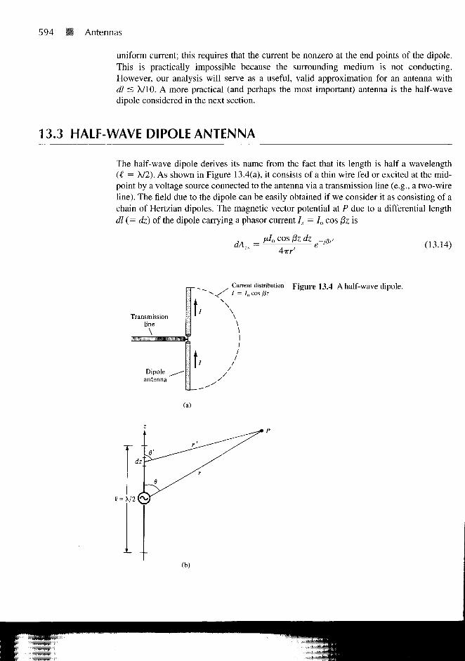
13.3 HALF-WAVE DIPOLE ANTENNA
The half-wave dipole derives its name from the fact that its length is half a wavelength(€ = A/2). As shown in Figure 13.4(a), it consists of a thin wire fed or excited at the mid-point by a voltage source connected to the antenna via a transmission line (e.g., a two-wireline). The field due to the dipole can be easily obtained if we consider it as consisting of achain of Hertzian dipoles. The magnetic vector potential at P due to a differential lengthdl(= dz) of the dipole carrying a phasor current Is = Io cos fiz is
(13.14)
Transmissionline
Dipoleantenna
Current distribution Figure 13.4 A half-wave dipole./ = /„ cos /3z
t' \
(a)

13.3 HALF-WAVE DIPOLE ANTENNA 595
Notice that to obtain eq. (13.14), we have assumed a sinusoidal current distributionbecause the current must vanish at the ends of the dipole; a triangular current distributionis also possible (see Problem 13.4) but would give less accurate results. The actual currentdistribution on the antenna is not precisely known. It is determined by solving Maxwell'sequations subject to the boundary conditions on the antenna, but the procedure is mathe-matically complex. However, the sinusoidal current assumption approximates the distribu-tion obtained by solving the boundary-value problem and is commonly used in antenna
theory.If r S> €, as explained in Section 4.9 on electric dipoles (see Figure 4.21), then
r - r' = z cos i or
Thus we may substitute r' — r in the denominator of eq. (13.14) where the magnitudeof the distance is needed. For the phase term in the numerator of eq. (13.14), the dif-ference between fir and ftr' is significant, so we replace r' by r — z cos 6 and not r. Inother words, we maintain the cosine term in the exponent while neglecting it in the de-nominator because the exponent involves the phase constant while the denominator doesnot. Thus,
-W4
4irr
A/4(13.15)
j8z cos e cos fiz dz- A / 4
From the integral tables of Appendix A.8,
eaz cos bz dz =eaz {a cos bz + b sin bz)
Applying this to eq. (13.15) gives
Azs =
nloe~jl3rejl3zcose UP cos 0 cos (3z + ff sin ffz)A/4
- A / 4
(13.16)
Since 0 = 2x/X or (3 X/4 = TT/2 and -cos2 0 + 1 = sin2 0, eq. (13.16) becomes
A,, = - ^ " f ' \ [e^n)™\0 + 13)- e -^«)«»» ( 0 _ ft] ( 1 3 - 1 7 )
A-wrfi sin 0
Using the identity eJX + e~;;c = 2 cos x, we obtain
\- cos 6> )
(13.18)txloe
i&rcos I - c o s I
2Trrj3sin2 6

596 • Antennas
We use eq. (13.4) in conjunction with the fact that B^ = /*HS = V X As and V X H , =y'coeEs to obtain the magnetic and electric fields at far zone (discarding the 1/r3 and 1/r2
terms) as
(13.19)
Notice again that the radiation term of H^,s and E$s are in time phase and orthogonal.Using eqs. (13.9) and (13.19), we obtain the time-average power density as
cos2 ( — cos 6 (13.20)
8TTV sin2 $
The time-average radiated power can be determined as
2 COS22-K fw I ? / 2 COS2 I ^ COS
= 0 8x2r2 sin2 $r2 sin 0 d6 d<j>
2TT
(13.21)
sin i
JrT COS I — COS I
^-s—~d e
o sm0
where t\ = 120TT has been substituted assuming free space as the medium of propagation.Due to the nature of the integrand in eq. (13.21),
TT/2 COS - COS 6
sine
cos~l — cos I
de= I — — '-desin 0J0 "'" " Jitl2
This is easily illustrated by a rough sketch of the variation of the integrand with d. Hence
= 60/2
IT- c o s i
sin I(13.22)

13.3 HALF-WAVE DIPOLE ANTENNA S 597
Changing variables, u = cos 6, and using partial fraction reduces eq. (13.22) to
C O S 2 - T T
\-u2 du
= 307'
2 1 2 1COS —KU r , COS ~KU
2 2 j
du + \ — du1 + U 01 - u
(13.23)
Replacing 1 + u with v in the first integrand and 1 — u with v in the second results in
rad = 30/2,
= 30/2
, sin2—7TV
dv +L'0
2 S in 2 -7TV
2 sin -TTV
dv
(13.24)
Changing variables, w = irv, yields
2TT sin — w- dw
= 15/
= 15 / '
2 [ ^ (1 — COS
2! 4! 6! 8!
(13.25)
w2 w4 w6 w8
since cos w = l H 1 • •. Integrating eq. (13.25) term by term and2! 4! 6! 8!
evaluating at the limit leads to
2 f (2TT)2 (2TT)4 (2?r)6 (2TT)8
~ 1 5 / ° L 2(2!) ~ 4(4!) + 6(6!) ~ 8(8!)
= 36.56 ll
+ (13.26)
The radiation resistance Rrad for the half-wave dipole antenna is readily obtained fromeqs. (13.12) and (13.26) as
(13.27)

598 Antennas
Note the significant increase in the radiation resistance of the half-wave dipole over that ofthe Hertzian dipole. Thus the half-wave dipole is capable of delivering greater amounts ofpower to space than the Hertzian dipole.
The total input impedance Zin of the antenna is the impedance seen at the terminals ofthe antenna and is given by
~ "in (13.28)
where Rin = Rmd for lossless antenna. Deriving the value of the reactance Zin involves acomplicated procedure beyond the scope of this text. It is found that Xin = 42.5 0, soZin = 73 + y'42.5 0 for a dipole length £ = X/2. The inductive reactance drops rapidly tozero as the length of the dipole is slightly reduced. For € = 0.485 X, the dipole is resonant,with Xin = 0. Thus in practice, a X/2 dipole is designed such that Xin approaches zero andZin ~ 73 0. This value of the radiation resistance of the X/2 dipole antenna is the reason forthe standard 75-0 coaxial cable. Also, the value is easy to match to transmission lines.These factors in addition to the resonance property are the reasons for the dipole antenna'spopularity and its extensive use.
13.4 QUARTER-WAVE MONOPOLE ANTENNA
Basically, the quarter-wave monopole antenna consists of one-half of a half-wave dipoleantenna located on a conducting ground plane as in Figure 13.5. The monopole antenna isperpendicular to the plane, which is usually assumed to be infinite and perfectly conduct-ing. It is fed by a coaxial cable connected to its base.
Using image theory of Section 6.6, we replace the infinite, perfectly conducting groundplane with the image of the monopole. The field produced in the region above the groundplane due to the X/4 monopole with its image is the same as the field due to a X/2 wavedipole. Thus eq. (13.19) holds for the X/4 monopole. However, the integration in eq. (13.21)is only over the hemispherical surface above the ground plane (i.e., 0 < d < TT/2) becausethe monopole radiates only through that surface. Hence, the monopole radiates only half asmuch power as the dipole with the same current. Thus for a X/4 monopole,
- 18.28/2 (13.29)
and
IP ad
Figure 13.5 The monopole antenna.
"Image
^ Infinite conductingground plane
13.5 SMALL LOOP ANTENNA 599
or
Rmd = 36.5 0 (13.30)
By the same token, the total input impedance for a A/4 monopole is Zin = 36.5 + _/21.25 12.
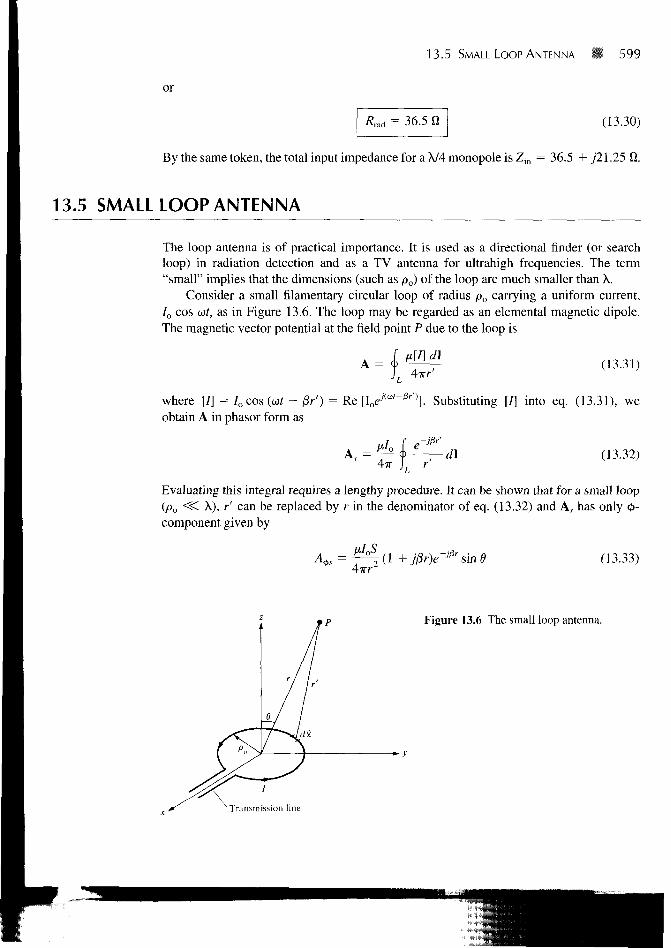
13.5 SMALL LOOP ANTENNA
The loop antenna is of practical importance. It is used as a directional finder (or searchloop) in radiation detection and as a TV antenna for ultrahigh frequencies. The term"small" implies that the dimensions (such as po) of the loop are much smaller than X.
Consider a small filamentary circular loop of radius po carrying a uniform current,Io cos co?, as in Figure 13.6. The loop may be regarded as an elemental magnetic dipole.The magnetic vector potential at the field point P due to the loop is
A =/*[/]</! (13.31)
where [7] = 7O cos (cor - /3r') = Re [loeji"' ISr)]. Substituting [7] into eq. (13.31), we
obtain A in phasor form as
e~jfir'e
Ait ]L r'(13.32)
Evaluating this integral requires a lengthy procedure. It can be shown that for a small loop(po <SC \ ) , r' can be replaced by r in the denominator of eq. (13.32) and As has only <f>-component given by
^<*sA-K?
(1 + j$r)e~i&r sin 6 (13.33)
Figure 13.6 The small loop antenna.
N Transmiss ion line
600 Antennas
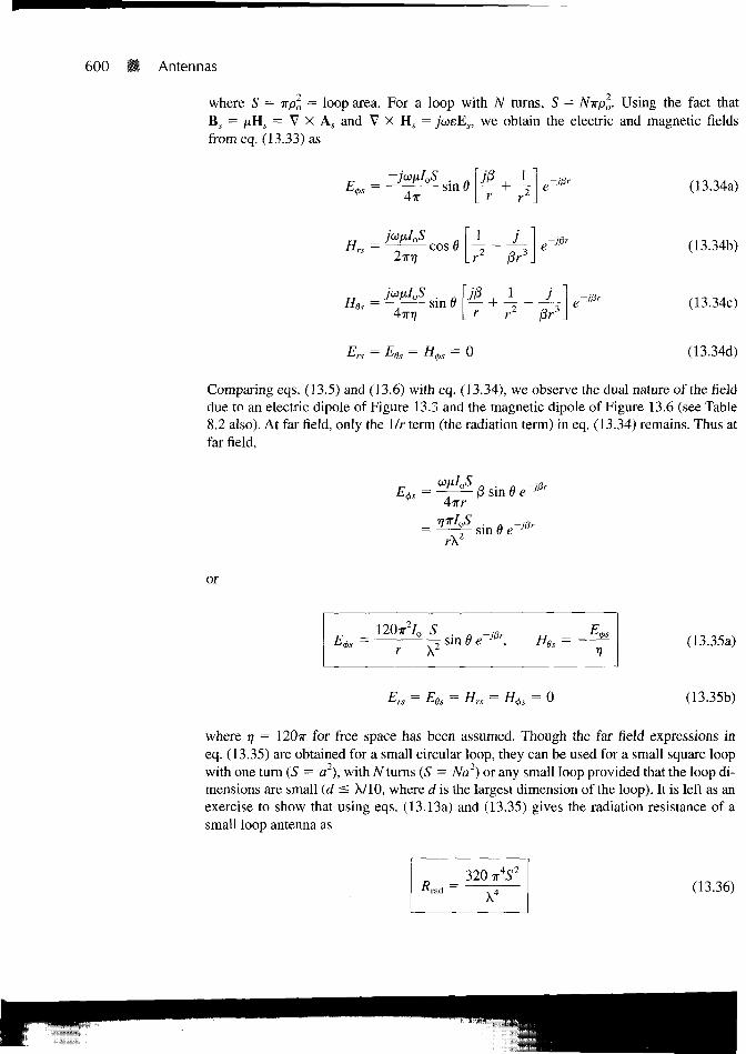
where S = wpl = loop area. For a loop with N turns, S = Nirpl. Using the fact thatBs = /xHs = VX A, and V X H S = ju>sEs, we obtain the electric and magnetic fieldsfrom eq. (13.33) as
Ai:sin I (13.34a)
2m,
4TTT/
/3r3
sin 0 J— + - r -2 )3rJ
ra - Eds - H<f>s - 0
(13.34b)
(13.34c)
(13.34d)
Comparing eqs. (13.5) and (13.6) with eq. (13.34), we observe the dual nature of the fielddue to an electric dipole of Figure 13.3 and the magnetic dipole of Figure 13.6 (see Table8.2 also). At far field, only the 1/r term (the radiation term) in eq. (13.34) remains. Thus atfar field,
4irr18 sin 6 e
r\2 sin o e
or
(13.35a)
- Hrs - - 0 (13.35b)
where 77 = 120TT for free space has been assumed. Though the far field expressions ineq. (13.35) are obtained for a small circular loop, they can be used for a small square loopwith one turn (S = a ) , with Af turns (S = Na2) or any small loop provided that the loop di-mensions are small (d < A/10, where d is the largest dimension of the loop). It is left as anexercise to show that using eqs. (13.13a) and (13.35) gives the radiation resistance of asmall loop antenna as
(13.36)

13.5 SMALL LOOP ANTENNA M 601
EXAMPLE 13.1 A magnetic field strength of 5 ^A/m is required at a point on 6 = TT/2, 2 km from anantenna in air. Neglecting ohmic loss, how much power must the antenna transmit if it is
(a) A Hertzian dipole of length X/25?
(b) A half-wave dipole?
(c) A quarter-wave monopole?
(d) A 10-turn loop antenna of radius po = X/20?
Solution:
(a) For a Hertzian dipole,
_ 7o/3 dl sin 6051 A
4irr
where dl = X/25 or 0 dl = = —. Hence,
5 X 1(T6 =4TT (2 X 10³) 105
or
Io = 0.5 A
'™H = 40TT2 I ^X
= 158 mW
40x2(0.5)2
(25)2
(b) For a X/2 dipole,
5 x
/o cos I — cos
2irr sin 6
/„ • 12TT(2 X
or
/„ = 207T mA
/^/? rad = 1/2(20TT)Z X 10~°(73)= 144 mW

602 B Antennas
(c) For a X/4 monopole,
as in part (b).
(d) For a loop antenna,
2
/ o = 20TT mA
= l/2I20Rmd = 1/2(20TT)2 X 10~6(36.56)
= 72 mW
*• /„ S .
r X2sin 8
For a single turn, S = •Kpo. For ,/V-turn, S = N-wp0. Hence,
or
5 X io - 6 = ^ ^ - ^2 X 103 L X
10
IOTT2 LPO
= 40.53 mA
— I X 10"3 =
= 320 7T6 X 100 iol =192-3fi
Z'rad = ^/o^rad = ~ (40.53)2 X 10"6 (192.3)
= 158 mW
PRACTICE EXERCISE 13.1
A Hertzian dipole of length X/100 is located at the origin and fed with a current of0.25 sin 108f A. Determine the magnetic field at
(a) r = X/5,0 = 30°
(b) r = 200X, 6 = 60°
Answer: (a) 0.2119 sin (10s? - 20.5°) a0 mA/m, (b) 0.2871 sin (l08t + 90°) a0
13.5 SMALL LOOP ANTENNA 603
EXAMPLE 13.2An electric field strength of 10 /uV/m is to be measured at an observation point 6 = ir/2,500 km from a half-wave (resonant) dipole antenna operating in air at 50 MHz.
(a) What is the length of the dipole?
(b) Calculate the current that must be fed to the antenna.
(c) Find the average power radiated by the antenna.
(d) If a transmission line with Zo = 75 0 is connected to the antenna, determine the stand-ing wave ratio.
Solution:
c 3 X 10⁸
(a) The wavelength X = - = r = 6 m./ 50 X 106
Hence, the length of the half-dipole is € = — = 3 m.
(b) From eq. (13.19),
r)Jo cos ( — cos 6
2-wr sin 6
or
2irr sin 9
r)o cos I — cos 6\2 j
10 X 10" 6 2TT(500 X 103) • (1)
120ir(l)
(c)
= 83.33 mA
Rmd = 73 Q
= \ (83.33)2 X 10-6 X 73
(d)
= 253.5 mW
F = — - (ZL = Zin in this case)z,£ + Zo
73 + y'42.5 - 75 _ - 2 + y'42.573 + y"42.5 + 75 ~42.55/92.69°
153.98/16.02
148 + y'42.5
= 0.2763/76.67°
s =1 + | r | 1 + 0.2763
- r 1 - 0.2763= 1.763

604 Antennas
PRACTICE EXERCISE 13.2
Repeat Example 13.2 if the dipole antenna is replaced by a X/4 monopole.
Answer: (a) 1.5m, (b) 83.33 mA, (c) 126.8 mW, (d) 2.265.
13.6 ANTENNA CHARACTERISTICS
Having considered the basic elementary antenna types, we now discuss some importantcharacteristics of an antenna as a radiator of electromagnetic energy. These characteristicsinclude: (a) antenna pattern, (b) radiation intensity, (c) directive gain, (d) power gain.
A. Antenna Patterns
An antenna pattern (or radiation pattern) is a ihrce-climensional plot of iis radia-tion ai fur field.
When the amplitude of a specified component of the E field is plotted, it is called the fieldpattern or voltage pattern. When the square of the amplitude of E is plotted, it is called thepower pattern. A three-dimensional plot of an antenna pattern is avoided by plotting sepa-rately the normalized \ES\ versus 0 for a constant 4> (this is called an E-plane pattern or ver-tical pattern) and the normalized \ES\ versus <t> for 8 = TT/2 (called the H-planepattern orhorizontal pattern). The normalization of \ES\ is with respect to the maximum value of the
so that the maximum value of the normalized \ES\ is unity.For the Hertzian dipole, for example, the normalized |iSj| is obtained from eq. (13.7) as
= |sin0| (13.37)
which is independent of <t>. From eq. (13.37), we obtain the £-plane pattern as the polarplot of j{8) with 8 varying from 0° to 180°. The result is shown in Figure 13.7(a). Note thatthe plot is symmetric about the z-axis (8 = 0). For the /f-plane pattern, we set 8 = TT/2 SOthat/(0) = 1, which is circle of radius 1 as shown in Figure 13.7(b). When the two plots ofFigures 13.7(a) and (b) are combined, we have a three-dimensional field pattern of Figure13.7(c), which has the shape of a doughnut.
A plot of the time-average power, |2Pave| = 2Pave, for a fixed distance r is the powerpattern of the antenna. It is obtained by plotting separately 2Pave versus 8 for constant <j> andS ave versus 4> for constant 8.
For the Hertzian dipole, the normalized power pattern is easily obtained from eqs.(13.37) or (13.9) as
/2(0) = sin2 0 (13.38)
which is sketched in Figure 13.8. Notice that Figures 13.7(b) and 13.8(b) show circlesbecause fi8) is independent of <j> and that the value of OP in Figure 13.8(a) is the relative

13.6 ANTENNA CHARACTERISTICS B 605
(a)
(c)
Figure 13.7 Field patterns of the Hertzian dipole: (a) normalized £-plane orvertical pattern (4> = constant = 0), (b) normalized ff-plane or horizontalpattern (6 = TT/2), (C) three-dimensional pattern.
Polar axis
(a) (b)
Figure 13.8 Power pattern of the Hertzian dipole: (a) 4> = constant = 0;(b) 6 = constant = T/2.

606 Antennas
average power for that particular 6. Thus, at point Q (0 = 45°), the average power is one-half the maximum average power (the maximum average power is at 6 = TT/2).
B. Radiation Intensity
The radiation intensity of an antenna is defined as
me, 0) = r2 g>a. (13.39)
From eq. (13.39), the total average power radiated can be expressed as
Sin 6 dd d$
= U{d,<j>) sin dd$d<t> (13.40)
2ir fir
U(6, </>) dU•=o Je=o
where dQ = sin 9 dd d(f> is the differential solid angle in steradian (sr). Hence the radiationintensity U(6, <f>) is measured in watts per steradian (W/sr). The average value of U(d, <j>) isthe total radiated power divided by 4TT sr; that is,
rrad
4?T(13.41)
C. Directive Gain
Besides the antenna patterns described above, we are often interested in measurable quan-tities such as gain and directivity to determine the radiation characteristics of an antenna.
The directive gain (i/0.6) of itn unlenna is a measure of the concentration of the ra-diated power in a particular direction (e. <p).
It may be regarded as the ability of the antenna to direct radiated power in a given direc-tion. It is usually obtained as the ratio of radiation intensity in a given direction (6, <f>) to theaverage radiation intensity, that is
(13.42)
13.6 ANTENNA CHARACTERISTICS 607
By substituting eq. (13.39) into eq. (13.42), 0 ^ may be expressed in terms of directivegain as
(13.43)=ave . ?
AirrThe directive gain GJfi, <j>) depends on antenna pattern. For the Hertzian dipole (as well asfor A/2 dipole and X/4 monopole), we notice from Figure 13.8 that 2Pave is maximum at6 = 7r/2 and minimum (zero) at 6 = 0 or TT. Thus the Hertzian dipole radiates power in adirection broadside to its length. For an isotropic antenna (one that radiates equally in alldirections), Gd = 1. However, such an antenna is not a physicality but an ideality.
The directivity I) of an antenna is ihe ratio of the maximum radiation intensity to theaverage radiaiion intensity.
Obviously, D is the maximum directive gain Gd, max. Thus
D = —— = Gd, max (13.44a)
or
D =•Prad
(13.44b)
D = 1 for an isotropic antenna; this is the smallest value D can have. For the Hertziandipole,
G/6,<j)) = 1.5 sin2 0, D = 1.5.
For the A/2 dipole,
(13.45)
Gd(d, </>) =
where i\ = 120x, /?rad = 73 fi, and
), D=\Mrad
ITCOS | — COS I
sin0
(13.46)
(13.47)
D. Power Gain
Our definition of the directive gain in eq. (13.42) does not account for the ohmic powerloss P( of the antenna. Pt is due to the fact that the antenna is made of a conductor with

608 Antennas
finite conductivity. As illustrated in Figure 13.9, if Pin is the total input power to theantenna,
Pin — +
+(13.48)
where 7in is the current at the input terminals and R( is the loss or ohmic resistance of theantenna. In other words, Pin is the power accepted by the antenna at its terminals during theradiation process, and Prad is the power radiated by the antenna; the difference between thetwo powers is P(, the power dissipated within the antenna.
We define the power gain Gp(6, <j>) of the antenna as
(13.49)
The ratio of the power gain in any specified direction to the directive gain in that directionis referred to as the radiation efficiency v\r of the antennas, that is
GPVr =
Introducing eq. (13.48) leads to
Vr =Pr,ad Vad
Rf(13.50)
For many antennas, r\r is close to 100% so that GP — Gd. It is customary to express direc-tivity and gain in decibels (dB). Thus
D(dB) = 101og,0£»
G (dB) = 10 log10 G
(13.51a)
(13.51b)
It should be mentioned at this point that the radiation patterns of an antenna areusually measured in the far field region. The far field region of an antenna is commonlytaken to exist at distance r > rmin where
2dz
(13.52)
Figure 13.9 Relating P-m, P(, and Prad.
Prad
13.6 ANTENNA CHARACTERISTICS 609
and d is the largest dimension of the antenna. For example, d = I for the electric dipoleantenna and d = 2p0 for the small loop antenna.
EXAMPLE 13.3 Show that the directive gain of the Hertzian dipole is
Gd(0, <£) = 1.5 sin2 6
and that of the half-wave dipole is
cos ( — cos 6Gd(9,<t>) = 1 - 6 4 —
sin (
Solution:
From eq. (13.42),
, <f>) =4TT/2(0)
f (6) d
(a) For the Hertzian dipole,
4TT sin2 6
sin3 6 d6 d<j)
4TT sin2 6
2TT (4/3)
= 1.5 sin2 6
as required.
(b) For the half-wave dipole,
4TT COS — cos
sin2
2lr rir cos I — cos 6 I dO d(f>
G/.9, <t>) =
From eq. (13.26), the integral in the denominator gives 27r(1.2188). Hence,
G/.8, 0) =4TT cos2! — cos 9
sin20 (1.2188)
= 1.64cos I — cos I
sin20
as required.
610 Antennas
PRACTICE EXERCISE 13.3
Calculate the directivity of
(a) The Hertzian monopole
(b) The quarter-wave monopole
Answer: (a) 3, (b) 3.28.
EXAMPLE 13.4 Determine the electric field intensity at a distance of 10 km from an antenna having a di-rective gain of 5 dB and radiating a total power of 20 kW.
Solution:
or
From eq. (13.43),
But
Hence,
5 = Gd(dB) = 101og10Grf
0.5 = log10 Gd -
GdPrad
= lO05 = 3.162
at, =u ave
op =° ave
4-irr
\E,2V
1207T(3.162)(20 X 103)E = =
2irr2 2TT[10 X 103]2
Es\ = 0.1948 V/m
PRACTICE EXERCISE 13.4
A certain antenna with an efficiency of 95% has maximum radiation intensity of0.5 W/sr. Calculate its directivity when
(a) The input power is 0.4 W
(b) The radiated power is 0.3 W
Answer: (a) 16.53, (b) 20.94.

EXAMPLE 13.5
13.6 ANTENNA CHARACTERISTICS
The radiation intensity of a certain antenna is
2 sin d sin3 0, 0 < 0 < TT, 0 < 0 < TT
611
U(8, 0) =0, elsewhere
Determine the directivity of the antenna.
Solution:
The directivity is defined as
D =ua.
From the given U,
= 2
_ _1_
1
~ 4TT
_ J_~ 2TT
9 «i=o •/e=o
s in 0 s in <j> s in 0 d<j>
s i n ' <j>d<t>o
= ^ - - (1 - cos 20) d0 (1 - cosz 0) rf(-cos (A)27r 4 2 4sin
2TT2
27r\2j\3j 3
/ COS (f)I cos io l 3
Hence
Z) =(1/3)
— 6
PRACTICE EXERCISE 13.5
Evaluate the directivity of an antenna with normalized radiation intensity
fsin 0, 0 < 0 < TT/2, 0 < 0 < 2TT[0, otherwise
Answer: 2.546.

612 B Antennas
13.7 ANTENNA ARRAYS
In many practical applications (e.g., in an AM broadcast station), it is necessary to designantennas with more energy radiated in some particular directions and less in other direc-tions. This is tantamount to requiring that the radiation pattern be concentrated in the di-rection of interest. This is hardly achievable with a single antenna element. An antennaarray is used to obtain greater directivity than can be obtained with a single antennaelement.
An antenna array is a group of radiating elements arranged so us to produce someparticular radiation characteristics.
It is practical and convenient that the array consists of identical elements but this isnot fundamentally required. We shall consider the simplest case of a two-elementarray and extend our results to the more complicated, general case of an N-elementarray.
Consider an antenna consisting of two Hertzian dipoles placed in free space along thez-axis but oriented parallel to the ;t-axis as depicted in Figure 13.10. We assume that thedipole at (0, 0, d/2) carries current Ils = I0/cx and the one at (0, 0, -d/2) carries currenths = 4 / 0 . where a is the phase difference between the two currents. By varying thespacing d and phase difference a, the fields from the array can be made to interfere con-structively (add) in certain directions of interest and interfere destructively (cancel) inother directions. The total electric field at point P is the vector sum of the fields due to theindividual elements. If P is in the far field zone, we obtain the total electric field at P fromeq. (13.7a) as
-'Is
COS0-,(13.53)
Note that sin 6 in eq. (13.7a) has been replaced by cos 6 since the element of Figure 13.3 isz-directed whereas those in Figure 13.10 are x-directed. Since P is far from the array,
Figure 13.10 A two-element array.

#i — 9 — 62 and ae< — ae
we use
13.7 ANTENNA ARRAYS S§ 613
i. In the amplitude, we can set rx — r = r2 but in the phase,
drx — r cos I
r2 — r + r cos i
(13.54a)
(13.54b)
Thus eq. (13.53) becomes
4x r->a/2j
4?r r cos cos \-L2
cos
(13.55)
Comparing this with eq. (13.7a) shows that the total field of an array is equal to the field ofsingle element located at the origin multiplied by an array factor given by
AF = 2 cos | - (/tacos 8 + u)\ eja/2 (13.56)
Thus, in general, the far field due to a two-element array is given by
E (total) = (E due to single element at origin) X (array factor) (13.57)
Also, from eq. (13.55), note that |cos d\ is the radiation pattern due to a single elementwhereas the normalized array factor, |cos[l/2(|8Jcos 6 + a)]\, is the radiation pattern ofthe array if the elements were isotropic. These may be regarded as "unit pattern" and"group pattern," respectively. Thus the "resultant pattern" is the product of the unit patternand the group pattern, that is,
Resultant pattern = Unit pattern X Group pattern (13.58)
This is known as pattern multiplication. It is possible to sketch, almost by inspection, thepattern of an array by pattern multiplication. It is, therefore, a useful tool in the design ofan array. We should note that while the unit pattern depends on the type of elements thearray is comprised of, the group pattern is independent of the element type so long as thespacing d and phase difference a, and the orientation of the elements remain the same.
Let us now extend the results on the two-element array to the general case of an N-element array shown in Figure 13.11. We assume that the array is linear in that the ele-ments are spaced equally along a straight line and lie along the z-axis. Also, we assume thatthe array is uniform so that each element is fed with current of the same magnitude but ofprogressive phase shift a, that is, Ils = /O//0,12s = Io/u, I3s = 7o/2q, and so on. We aremainly interested in finding the array factor; the far field can easily be found from eq.
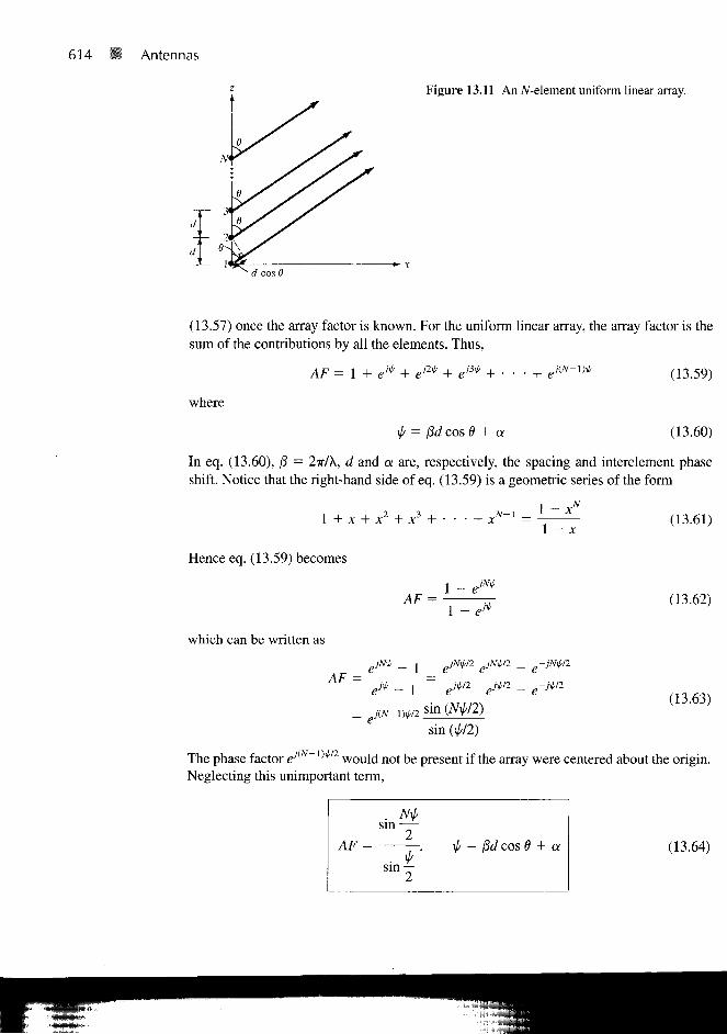
614 Antennas
Figure 13.11 An iV-element uniform linear array.
- d cos 6
(13.57) once the array factor is known. For the uniform linear array, the array factor is thesum of the contributions by all the elements. Thus,
AF = 1 + eJ4r + ej2>p + + eAN-1)4,
where
= (3d cos 6 + a
(13.59)
(13.60)
In eq. (13.60), fi = 2x/X, d and a are, respectively, the spacing and interelement phaseshift. Notice that the right-hand side of eq. (13.59) is a geometric series of the form
1 + x + x2 + x3
Hence eq. (13.59) becomes
1 - x
AF =1 -
(13.61)
(13.62)
which can be written as
AF =_ e-jN4,/2
sin (Aty/2)
sin (\l//2)
(13.63)
The phase factor eJ(N l)*n would not be present if the array were centered about the origin.Neglecting this unimportant term,
(13.64)AF = \b = fid cos 6 + a
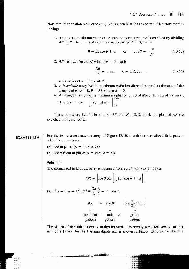
13.7 ANTENNA ARRAYS 615
Note that this equation reduces to eq. (13.56) when N = las, expected. Also, note the fol-lowing:
1. AF has the maximum value of TV; thus the normalized AF is obtained by dividingAF by N. The principal maximum occurs when \J/ = 0, that is
0 = fid cos 6 + a or
2. AF has nulls (or zeros) when AF = 0, that is
Nip
cos 0 = — a
Yd
—- = ±/br, k= 1,2, 3 , . . .
(13.65)
(13.66)
where k is not a multiple of N.3. A broadside array has its maximum radiation directed normal to the axis of the
array, that is, \p = 0, $ = 90° so that a = 0.4. An end-fire array has its maximum radiation directed along the axis of the array,
that is, \p = 0, B = so that a =
These points are helpful in plotting AF. For N=2,3, and 4, the plots of AF aresketched in Figure 13.12.
EXAMPLE 13.6 For the two-element antenna array of Figure 13.10, sketch the normalized field patternwhen the currents are:
(a) Fed in phase (a = 0), d = A/2
(b) Fed 90° out of phase (a = TT/2), d = A/4
Solution:
The normalized field of the array is obtained from eqs. (13.55) to (13.57) as
cos 6 cos - (0d cos 8 + a)
(a) If a = 0, d = A/2,13d = - ^ - = TT. Hence,A 2
1resultantpattern
= |cos0|
1= unit X
pattern
cos — (cos 6)
1grouppattern
The sketch of the unit pattern is straightforward. It is merely a rotated version of thatin Figure 13.7(a) for the Hertzian dipole and is shown in Figure 13.13(a). To sketch a

616 m Antennas
0 TT/2 IT 3TT/2 2TT
Figure 13.12 Array factor for uniform linear array.
1.08 T-V^S.—
group pattern requires that we first determine its nulls and maxima. For the nulls (orzeros),
(-K \ i „ IT 3fcos — cos 0 = 0 -»— cos 0 = ± —, ± — , . . .
\2 ) 2 2 2
or
For the maxima,
or
0 = 0°, 180°
cos ( — cos 0 ) = 1 —» cos 0 = 0
0 = 90°

unit pattern(a)
x X
13.7 ANTENNA ARRAYS • 617
group pattern(b)
resultant pattern(c)
Figure 13.13 For Example 13.6(a); field patterns in the plane containing theaxes of the elements.
The group pattern is as shown in Figure 13.12(b). It is the polar plot obtained by sketching
for0 = 0°, 5°, 10°, 15°,. . . . , 360° and incorporating the nulls andcos ( — cos 0
maxima at 0 = 0°, 180° and 0 = 90°, respectively. Multiplying Figure 13.13(a) withFigure 13.13(b) gives the resultant pattern in Figure 13.13(c). It should be observed thatthe field patterns in Figure 13.13 are in the plane containing the axes of the elements. Notethat: (1) In the yz-plane, which is normal to the axes of the elements, the unit pattern (= 1)is a circle [see Figure 13.7(b)] while the group pattern remains as in Figure 13.13(b); there-fore, the resultant pattern is the same as the group pattern in this case. (2) In the xy-plane,0 = 7r/2, SO the unit pattern vanishes while the group pattern (= 1) is a circle.
(b) If a = TT/2, d = A/4, and fid = — - = -A 4 2
c o s — ( c o s 0 + 1 )
Igrouppattern
I iresultant = unit Xpattern pattern
The unit pattern remains as in Figure 13.13(a). For the group pattern, the null occurs when
COS j (1 + COS 6>) = 0 -> - (1 + COS 0) = ± y , ±-y, . . .
or
cos 8 = 1 -» 0 = 0
The maxima and minima occur when
— cos - (1 + cos 0) = 0 -» sin 0 sin - (1 + cos 0) = 0dd I 4 J 4
sin0 = O->0 = 0°, 180°

618 • Antennas
x X
unit pattern(a)
group pattern(b)
resultant pattern(c)
Figure 13.14 For Example 13.6(b); field patterns in the plane containing the axes ofthe elements.
and
sin — (1 + cos 6) = 0 —> cos I= - 1 or 6 = 180°
Each field pattern is obtained by varying 0 = 0°, 5°, 10°, 15°,. . ., 180°. Note that8 = 180° corresponds to the maximum value of AF, whereas d = 0° corresponds to thenull. Thus the unit, group, and resultant patterns in the plane containing the axes of the el-ements are shown in Figure 13.14. Observe from the group patterns that the broadsidearray (a = 0) in Figure 13.13 is bidirectional while the end-fire array (a = (3d) in Figure13.14 is unidirectional.
PRACTICE EXERCISE 13.6
Repeat Example 13.6 for cases when:
(a) a = IT, d = A/2, (b) a = -TT/2, d = A/4.
Answer: See Figure 13.15.
EXAMPLE 13.7 Consider a three-element array that has current ratios 1:2:1 as in Figure 13.16(a). Sketchthe group pattern in the plane containing the axes of the elements.
Solution:
For the purpose of analysis, we split the middle element in Figure 13.16(a) carrying current27/0° into two elements each carrying current 1/0^. This results in four elements insteadof three as shown in Figure 13.16(b). If we consider elements 1 and 2 as a group and ele-ments 3 and 4 as another group, we have a two-element array of Figure 13.16(c). Each
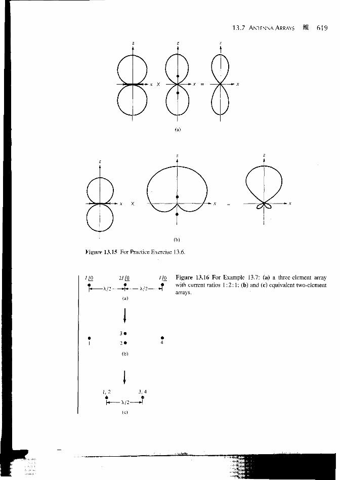
13.7 ANTENNA ARRAYS • 619
x X
x X
(a)
(b)
Figure 13.15 For Practice Exercise 13.6.
//0 2IlQ_ //O Figure 13.16 For Example 13.7: (a) a three-element array• ,_ * ^ ; i J with current ratios 1:2:1; (b) and (c) equivalent two-element
-X/2- • X / 2 -
(a)arrays.
3 *
2»
(b)
4
1,2 3 , 4* *
(c)
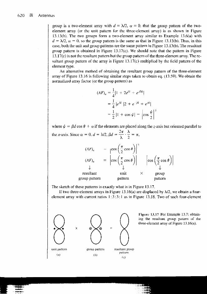
620 Antennas
group is a two-element array with d — X/2, a = 0, that the group pattern of the two-element array (or the unit pattern for the three-element array) is as shown in Figure13.13(b). The two groups form a two-element array similar to Example 13.6(a) withd = X/2, a = 0, so the group pattern is the same as that in Figure 13.13(b). Thus, in thiscase, both the unit and group patterns are the same pattern in Figure 13.13(b). The resultantgroup pattern is obtained in Figure 13.17(c). We should note that the pattern in Figure13.17(c) is not the resultant pattern but the group pattern of the three-element array. The re-sultant group pattern of the array is Figure 13.17(c) multiplied by the field pattern of theelement type.
An alternative method of obtaining the resultant group pattern of the three-elementarray of Figure 13.16 is following similar steps taken to obtain eq. (13.59). We obtain thenormalized array factor (or the group pattern) as
(AF)n = -
_\_~ 4_ J_~ 2
2el*
e'1*
c o s -
where yj/ = fid cos d + a if the elements are placed along the z-axis but oriented parallel to2TT X
the x-axis. Since a = 0, d = X/2, fid = — • — = x,X 2
(AF)n
{AF)n
Iresultant
group pattern
cos ( — cos 6
cos | — cos i
4unit
patternX
cos ( — cos 0
4grouppattern
The sketch of these patterns is exactly what is in Figure 13.17.If two three-element arrays in Figure 13.16(a) are displaced by X/2, we obtain a four-
element array with current ratios 1:3:3:1 as in Figure 13.18. Two of such four-element
Figure 13.17 For Example 13.7; obtain-ing the resultant group pattern of thethree-element array of Figure 13.16(a).
unit pattern
(a)
roup pattern
(b)
resultant grouppattern
(0

13.8 EFFECTIVE AREA AND THE FRIIS EQUATION 621
3//0_
-X/2-
/ [0_ Figure 13.18 A four-elementarray with current ratios 1:3:3:1;for Practice Exercise 13.7.
arrays, displaced by X/2, give a five-element array with current ratios 1:4:6:4:1. Contin-uing this process results in an /^-element array, spaced X/2 and (N - l)X/2 long, whosecurrent ratios are the binomial coefficients. Such an array is called a linear binomial army.
PRACTICE EXERCISE 13.7
(a) Sketch the resultant group pattern for the four-element array with current ratios1:3:3:1 shown in Figure 13.18.
(b) Derive an expression for the group pattern of a linear binomial array of N ele-ments. Assume that the elements are placed along the z-axis, oriented parallel to the;t-axis with spacing d and interelement phase shift a.
Answer: (a) See Figure 13.19, (b) c o s - , where if/ — fid cos d + a.
Figure 13.19 For Practice Exercise 13.7(a).
'13.8 EFFECTIVE AREA AND THE FRIIS EQUATION
In a situation where the incoming EM wave is normal to the entire surface of a receivingantenna, the power received is
Pr = (13.67)
But in most cases, the incoming EM wave is not normal to the entire surface of theantenna. This necessitates the idea of the effective area of a receiving antenna.
The concept of effective area or effective aperture (receiving cross section of anantenna) is usually employed in the analysis of receiving antennas.
The effective area A, of u receiving antenna is the ratio of the time-average powerreceived Pr (or delivered to (he load, to be strict) to the time-average power density;?„,, of the incident wave at the antenna.

622 Antennas
That is
PrOb•J avp
(13.68)
From eq. (13.68), we notice that the effective area is a measure of the ability of the antennato extract energy from a passing EM wave.
Let us derive the formula for calculating the effective area of the Hertzian dipoleacting as a receiving antenna. The Thevenin equivalent circuit for the receiving antenna isshown in Figure 13.20, where Voc is the open-circuit voltage induced on the antenna termi-nals, Zin = 7?rad + jXin is the antenna impedance, and ZL = RL + jXL is the external loadimpedance, which might be the input impedance to the transmission line feeding theantenna. For maximum power transfer, ZL = Z*n and XL = —Xin. The time-average powerdelivered to the matched load is therefore
'rad
|v«(13.69)
8 D"ra .
For the Hertzian dipole, Rmd = S0ir2(dl/X)2 and yoc = Edl where E is the effective fieldstrength parallel to the dipole axis. Hence, eq. (13.69) becomes
Pr =E\2
640TT2
The time-average power at the antenna is
_ave "
2TJ0 240TT
Inserting eqs. (13.70) and (13.71) in eq. (13.68) gives
3X2 X2
A L 5
(13.70)
(13.71)
or
(13.72)
Figure 13.20 Thevenin equivalent of a receivingantenna.

13.8 EFFECTIVE AREA AND THE FRIIS EQUATION 623
where D = 1.5 is the directivity of the Hertzian dipole. Although eq. (13.72) was derivedfor the Hertzian dipole, it holds for any antenna if D is replaced by GJfi, (j>). Thus, ingeneral
(13.73)
Now suppose we have two antennas separated by distance r in free space as shown inFigure 13.21. The transmitting antenna has effective area Aet and directive gain Gdt, andtransmits a total power P, (= Prli<i). The receiving antenna has effective area of Aer and di-rective gain Gdn and receives a total power of Pr. At the transmitter,
4rU
P
or
op =ave
p(13.74)
By applying eqs. (13.68) and (13.73), we obtain the time-average power received as
P = Op A = ^— C,,r r ^ ave ^er * ^dr
Substituting eq. (13.74) into eq. (13.75) results in
(13.75)
(13.76)
This is referred to as the Friis transmission formula. It relates the power received by oneantenna to the power transmitted by the other, provided that the two antennas are separatedby r > 2d2l\, where d is the largest dimension of either antenna [see eq. 13.52)]. There-fore, in order to apply the Friis equation, we must make sure that the two antennas are inthe far field of each other.
Transmitter Receiver
H r-
Figure 13.21 Transmitting and receiving antennas in free space.
624 Antennas
EXAMPLE 13.8Find the maximum effective area of a A/2 wire dipole operating at 30 MHz. How muchpower is received with an incident plane wave of strength 2 mV/m.
Solution:
c 3 X 10⁸
A = - = T = 10m/ 30 X 106
Gd(6, 0)raax = 1.64
102
(1.64)= 13.05 m2
p = Op A - — A
_ V
( 2 X 1 0 )
= 1.64/(0)
240TT13.05 = 71.62 nW
PRACTICE EXERCISE 13.8
Determine the maximum effective area of a Hertzian dipole of length 10 cm operat-ing at 10 MHz. If the antenna receives 3 [iW of power, what is the power density ofthe incident wave?
Answer: 1.074 m2, 2.793 MW/m2
EXAMPLE 13.9The transmitting and receiving antennas are separated by a distance of 200 A and have di-rective gains of 25 and 18 dB, respectively. If 5 mW of power is to be received, calculatethe minimum transmitted power.
Solution:
Given that Gdt (dB) = 25 dB = 10 log10 Gdt,
Gdt = 1025 = 316.23
Similarly,
Gdr (dB) = 18 db or Gdr = 1 0 ° = 63.1
13.9 THE RADAR EQUATION 625
Using the Friis equation, we have
or
P = P
Pr ~ GdrGdt [ — J P,
47rr12
= 5 x 10~3
= 1.583 W
J GdrGdt4TT X 200 X
X
1(63.1X316.23)
PRACTICE EXERCISE 13.9
An antenna in air radiates a total power of 100 kW so that a maximum radiated elec-tric field strength of 12 mV/m is measured 20 km from the antenna. Find: (a) its di-rectivity in dB, (b) its maximum power gain if r]r =
Answer: (a) 3.34 dB, (b) 2.117.
13.9 THE RADAR EQUATION
Radars are electromagnetic devices used for detection and location of objects. The termradar is derived from the phrase radio detection and ranging. In a typical radar systemshown in Figure 13.22(a), pulses of EM energy are transmitted to a distant object. Thesame antenna is used for transmitting and receiving, so the time interval between the trans-mitted and reflected pulses is used to determine the distance of the target. If r is the dis-
k Target a
Figure 13.22 (a) Typical radar system,(b) simplification of the system in(a) for calculating the target crosssection a.
(b)

626 Antennas
tance between the radar and target and c is the speed of light, the elapsed time between thetransmitted and received pulse is 2r/c. By measuring the elapsed time, r is determined.
The ability of the target to scatter (or reflect) energy is characterized by the scatteringcross section a (also called the radar cross section) of the target. The scattering crosssection has the units of area and can be measured experimentally.
The scattering cross section is the equivalent area intercepting that amount olpower that, when scattering isotropicall). produces at the radar a power density,which is equal to thai scattered (or reflected) by the actual target.
That is,
= lim4-irr2
or
<3/>a = lim 4xr2 —-
9>(13.77)
where SP, is the incident power density at the target T while 3 \ is the scattered powerdensity at the transreceiver O as in Figure 13.22(b).
From eq. (13.43), the incident power density 2P, at the target Tis
op = op = d p J^ i "^ ave , 9 * rad
4TIT
The power received at transreceiver O is
(13.78)
or
—Aer
(13.79)
Note that 2P, and 9 \ are the time-average power densities in watts/m2 and Prad and Pr arethe total time-average powers in watts. Since Gdr = Gdt — Gd and Aer = Aet = Ae, substi-tuting eqs. (13.78) and (13.79) into eq. (13.77) gives
a = (4irr2)2 1Gd
or
AeaGdPmd
(4irr2)2
(13.80a)
(13.80b)
13.9 THE RADAR EQUATION 627
TABLE 13.1 Designationsof Radar Frequencies
Designation
UHF
L
S
C
X
Ku
K
Millimeter
Frequency
300-1000 MHz
1000-2000 MHz
2000^000 MHz
4000-8000 MHz
8000-12,500 MHz
12.5-18 GHz
18-26.5 GHz>35 GHz
From eq. (13.73), Ae = \2GJAi;. Hence,
(13.81)
This is the radar transmission equation for free space. It is the basis for measurement ofscattering cross section of a target. Solving for r in eq. (13.81) results in
(13.82)
Equation (13.82) is called the radar range equation. Given the minimum detectable powerof the receiver, the equation determines the maximum range for a radar. It is also useful forobtaining engineering information concerning the effects of the various parameters on theperformance of a radar system.
The radar considered so far is the monostatic type because of the predominance of thistype of radar in practical applications. A bistatic radar is one in which the transmitter andreceiver are separated. If the transmitting and receiving antennas are at distances rx and r2
from the target and Gdr ¥= Gdt, eq. (13.81) for bistatic radar becomes
GdtGdr
4TTrad (13.83)
Radar transmission frequencies range from 25 to 70,000 MHz. Table 13.1 shows radarfrequencies and their designations as commonly used by radar engineers.
EXAMPLE 13.10An S-band radar transmitting at 3 GHz radiates 200 kW. Determine the signal powerdensity at ranges 100 and 400 nautical miles if the effective area of the radar antenna is9 m2. With a 20-m2 target at 300 nautical miles, calculate the power of the reflected signalat the radar.
628 Antennas
Solution:
The nautical mile is a common unit in radar communications.
1 nautical mile (nm) = 1852 m
c 3 X 10⁸
/ 3 X 10-
r -X2 et (0.1):
= 0.1m
9 = 3600?r
For r = 100 nm = 1.852 X 10⁵m
ad 3600TT X 200 X 103
4TIT2 4TT(1 .852) 2 X 1010
= 5.248 mW/m2
For r = 400 nm = 4 (1.852 X 10⁵) m
5.248
(4)2 = 0.328 mW/m2
Aea Gd P r a d
Using eq. (13.80b)
where r = 300 nm = 5.556 X 10⁵ m
_ 9 X 20 X 36007T X 200 X 103
[4TT X 5.5562]2 X 10²⁰
The same result can be obtained using eq. (13.81).
= 2.706 X 10"14W
PRACTICE EXERCISE 13.10
A C-band radar with an antenna 1.8 m in radius transmits 60 kW at a frequency of6000 MHz. If the minimum detectable power is 0.26 mW, for a target cross sectionof 5 m2, calculate the maximum range in nautical miles and the signal power densityat half this range. Assume unity efficiency and that the effective area of the antennais 70% of the actual area.
Answer: 0.6309 nm, 500.90 W/m2.

SUMMARY 629
SUMMARY 1. We have discussed the fundamental ideas and definitions in antenna theory. The basictypes of antenna considered include the Hertzian (or differential length) dipole, thehalf-wave dipole, the quarter-wave monopole, and the small loop.
2. Theoretically, if we know the current distribution on an antenna, we can find the re-tarded magnetic vector potential A, and from it we can find the retarded electromag-netic fields H and E using
H = V X — , E = T, H X a*
The far-zone fields are obtained by retaining only \lr terms.3. The analysis of the Hertzian dipole serves as a stepping stone for other antennas. The
radiation resistance of the dipole is very small. This limits the practical usefulness ofthe Hertzian dipole.
4. The half-wave dipole has a length equal to X/2. It is more popular and of more practi-cal use than the Hertzian dipole. Its input impedance is 73 + J42.5 fi.
5. The quarter-wave monopole is essentially half a half-wave dipole placed on a con-ducting plane.
6. The radiation patterns commonly used are the field intensity, power intensity, and ra-diation intensity patterns. The field pattern is usually a plot of \ES\ or its normalizedform flft). The power pattern is the plot of 2Pave or its normalized form/2(0).
7. The directive gain is the ratio of U(9, <f>) to its average value. The directivity is themaximum value of the directive gain.
8. An antenna array is a group of radiating elements arranged so as to produce someparticular radiation characteristics. Its radiation pattern is obtained by multiply-ing the unit pattern (due to a single element in the group) with the group pattern,which is the plot of the normalized array factor. For an TV-element linear uniformarray,
AF =
where \j/ = 13d cos 9 + a, 0 = 2%/X, d = spacing between the elements, and a = in-terelement phase shift.
9. The Friis transmission formula characterizes the coupling between two antennas interms of their directive gains, separation distance, and frequency of operation.
10. For a bistatic radar (one in which the transmitting and receiving antennas are sepa-rated), the power received is given by
4TTrJ
aPn•ad
For a monostatic radar, r, = r2 = r and Gdt = Gdr.

630 Antennas
13.1 An antenna located in a city is a source of radio waves. How much time does it take thewave to reach a town 12,000 km away from the city?
(a) 36 s
(b) 20 us
(c) 20 ms
(d) 40 ms
(e) None of the above
13.2 In eq. (13.34), which term is the radiation term?
(a) 1/rterm
(b) l/r2term
(c) IIr" term
(d) All of the above
13.3 A very small thin wire of length X/100 has a radiation resistance of
(a) = 0 G
(b) 0.08 G
(c) 7.9 G
(d) 790 0
13.4 A quarter-wave monopole antenna operating in air at frequency 1 MHz must have anoverall length of
(a) € » X
(b) 300 m
(c) 150 m
(d) 75 m
(e) ( <sC X
13.5 If a small single-turn loop antenna has a radiation resistance of 0.04 G, how many turnsare needed to produce a radiation resistance of 1 G?
(a) 150
(b) 125
(c) 50
(d) 25
(e) 5

REVIEW QUESTIONS 631
13.6 At a distance of 8 km from a differential antenna, the field strength is 12 /iV/m. The fieldstrength at a location 20 km from the antenna is
(a) 75/xV/m
(b) 30,xV/m
(c) 4.8/xV/m
(d) 1.92/zV/m
13.7 An antenna has f/max = 10 W/sr, l/ave = 4.5 W/sr, and i\r = 95%. The input power tothe antenna is
(a) 2.222 W
(b) 12.11 W
(c) 55.55 W
(d) 59.52 W
13.8 A receiving antenna in an airport has a maximum dimension of 3 m and operates at 100MHz. An aircraft approaching the airport is 1/2 km from the antenna. The aircraft is inthe far field region of the antenna.
(a) True
(b) False
13.9 A receiving antenna is located 100 m away from the transmitting antenna. If the effectivearea of the receiving antenna is 500 cm2 and the power density at the receiving locationis 2 mW/m2, the total power received is:
(a) lOnW
(b) 100 nW
(c) 1/xW
(d) 10 ^W
(e) 100 ^W
13.10 Let R be the maximum range of a monostatic radar. If a target with radar cross section of5 m2 exists at R/2, what should be the target cross section at 3R/2 to result in an equalsignal strength at the radar?
(a) 0.0617 m2
(b) 0.555 m2
(c) 15 m2
(d) 45 m2
(e) 405 m2
Answers: 13.Id, 13.2a, 13.3b, 13.4d, 13.5e, 13.6c, 13.7d, 13.8a, 13.9e, 13.10e.
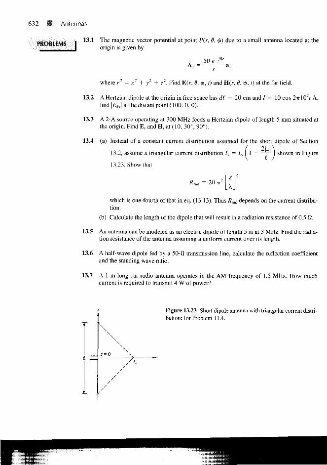
632 • Antennas
PROBLEMS I13.1 The magnetic vector potential at point P(r, 8, <j>) due to a small antenna located at the
origin is given by
50 e->Br
A
where r2 = x2 + y2 + z2• Find E(r, 6, <j>, t) and H(r, d, <j>, i) at the far field.
13.2 A Hertzian dipole at the origin in free space has di = 20 c m and 7 = 1 0 cos 2irl07t A ,find \E6s\ at the distant point (100 , 0, 0 ) .
13.3 A 2-A source operating at 300 MHz feeds a Hertzian dipole of length 5 mm situated atthe origin. Find Es and H,. at (10, 30°, 90°).
13.4 (a) Instead of a constant current distribution assumed for the short dipole of Section
13.2, assume a triangular current distribution 7, = 7O I 1 — j shown in Figure
13.23. Show that
?rad = 2 0 7TZ I -
which is one-fourth of that in eq. (13.13). Thus Rmd depends on the current distribu-tion.
(b) Calculate the length of the dipole that will result in a radiation resistance of 0.5 0.
13.5 An antenna can be modeled as an electric dipole of length 5 m at 3 MHz. Find the radia-tion resistance of the antenna assuming a uniform current over its length.
13.6 A half-wave dipole fed by a 50-0 transmission line, calculate the reflection coefficientand the standing wave ratio.
13.7 A 1-m-long car radio antenna operates in the AM frequency of 1.5 MHz. How muchcurrent is required to transmit 4 W of power?
Figure 13.23 Short dipole antenna with triangular current distri-bution; for Problem 13.4.
PROBLEMS • 633
*13.8 (a) Show that the generated far field expressions for a thin dipole of length € carrying si-nusoidal current Io cos @z are
,-/3rCos^ Yc0St)J ~ c o s y2-wr sin 8
[Hint: Use Figure 13.4 and start with eq. (13.14).]
(b) On a polar coordinate sheet, plot fifi) in part (a) for € = X, 3X/2 and 2X.
*13.9 For Problem 13.4.
(a) Determine E, and H s at the far field
(b) Calculate the directivity of the dipole
*13.10 An antenna located on the surface of a flat earth transmits an average power of 200 kW.Assuming that all the power is radiated uniformly over the surface of a hemisphere withthe antenna at the center, calculate (a) the time-average Poynting vector at 50 km, and(b) the maximum electric field at that location.
13.11 A 100-turn loop antenna of radius 20 cm operating at 10 MHz in air is to give a 50 mV/mfield strength at a distance 3 m from the loop. Determine
(a) The current that must be fed to the antenna
(b) The average power radiated by the antenna
13.12 Sketch the normalized E-field and //-field patterns for
(a) A half-wave dipole
(b) A quarter-wave monopole
13.13 Based on the result of Problem 13.8, plot the vertical field patterns of monopole antennasof lengths € = 3X/2, X, 5X/8. Note that a 5X/8 monopole is often used in practice.
13.14 In free space, an antenna has a far-zone field given by
where /3 = wV/xoeo. Determine the radiated power.
13.15 At the far field, the electric field produced by an antenna is
E s = — e~j/3r cos 6 cos <j> az
Sketch the vertical pattern of the antenna. Your plot should include as many points aspossible.

634 Antennas
13.16 For an Hertzian dipole, show that the time-average power density is related to the radia-tion power according to
1.5 sin20 _
4irr
13.17 At the far field, an antenna produces
2 sin 6 cos 4>ave a r W/m2, 0 < 6 < x, 0 < </> < x/2
Calculate the directive gain and the directivity of the antenna.
13.18 From Problem 13.8, show that the normalized field pattern of a full-wave (€ = X)antenna is given by
cos(x cos 6) + 1sin0
Sketch the field pattern.
13.19 For a thin dipole A/16 long, find: (a) the directive gain, (b) the directivity, (c) the effec-tive area, (d) the radiation resistance.
13.20 Repeat Problem 13.19 for a circular thin loop antenna A/12 in diameter.
13.21 A half-wave dipole is made of copper and is of diameter 2.6 mm. Determine the effi-ciency of the dipole if it operates at 15 MHz.Hint: Obtain R( from R(/Rdc = a/28; see Section 10.6.
13.22 Find C/ave, t/max, and D if:
(a) Uifi, 4>) = sin2 20, 0 < 0 < x, 0 < 0 < 2TT
(b) Uifi, <t>) = 4 esc2 20, TT/3 < 0 < x/2, 0 < <j> < x
(c) U(6, 4>) = 2 sin2 0 sin2 <j>, 0 < d < x, 0 < <t> < x
13.23 For the following radiation intensities, find the directive gain and directivity:
(a) U(6, 4>) = s in 2 0, 0 < 0 < x, 0 < <j> < 2x
(b) U(6, <t>) = 4 sin2 0 c o s 2 0 , O < 0 < T T , 0 < 0 < TT
(c) Uifi, <t>) = 10 cos2 0 sin2 4>/2, 0 < 0 < x, 0 < <f> < x/2
13.24 In free space, an antenna radiates a field
4TIT
at far field. Determine: (a) the total radiated power, (b) the directive gain at 0 = 60°.
13.25 Derive Es at far field due to the two-element array shown in Figure 13.24. Assume thatthe Hertzian dipole elements are fed in phase with uniform current /o cos cot.

PROBLEMS 635
Figure 13.24 Two-element array of Problem13.25.
-*-y
13.26 An array comprises two dipoles that are separated by one wavelength. If the dipoles arefed by currents of the same magnitude and phase,
(a) Find the array factor.
(b) Calculate the angles where the nulls of the pattern occur.
(c) Determine the angles where the maxima of the pattern occur.
(d) Sketch the group pattern in the plane containing the elements.
13.27 An array of two elements that are fed by currents that are 180° out of phase with eachother. Plot the group pattern if the elements are separated by: (a) d = A/4, (b) d = X/2
13.28 Sketch the group pattern in the xz-plane of the two-element array of Figure 13.10 with
(a) d = A, a = -all
(b) d = A/4, a = 3TT/4
(c) d = 3A/4, a = 0
13.29 An antenna array consists of N identical Hertzian dipoles uniformly located along the z-axis and polarized in the ^-direction. If the spacing between the dipole is A/4, sketch thegroup pattern when: (a) N = 2, (b) N = 4.
13.30 Sketch the resultant group patterns for the four-element arrays shown in Figure 13.25.
- X / 2 - -X/2-
(a)
'12. l[0_ Figure 13.25 For Problem 13.30.
x/2-
'12.•X/4-
I jit 12
-X/4-
(b)
//3ir/2
-X/4-

636 • Antennas
13.31 For a 10-turn loop antenna of radius 15 cm operating at 100 MHz, calculate the effectivearea at $ = 30°, <j> = 90°.
13.32 An antenna receives a power of 2 /xW from a radio station. Calculate its effective area ifthe antenna is located in the far zone of the station where E = 50 mV/m.
13.33 (a) Show that the Friis transmission equation can be written as
"r _ AerAet
(b) Two half-wave dipole antennas are operated at 100 MHz and separated by 1 km. If80 W is transmitted by one, how much power is received by the other?
13.34 The electric field strength impressed on a half-wave dipole is 3 mV/m at 60 MHz. Cal-culate the maximum power received by the antenna. Take the directivity of the half-wavedipole as 1.64.
13.35 The power transmitted by a synchronous orbit satellite antenna is 320 W. If the antennahas a gain of 40 dB at 15 GHz, calculate the power received by another antenna with again of 32 dB at the range of 24,567 km.
13.36 The directive gain of an antenna is 34 dB. If the antenna radiates 7.5 kW at a distance of40 km, find the time-average power density at that distance.
13.37 Two identical antennas in an anechoic chamber are separated by 12 m and are orientedfor maximum directive gain. At a frequency of 5 GHz, the power received by one is 30dB down from that transmitted by the other. Calculate the gain of the antennas in dB.
13.38 What is the maximum power that can be received over a distance of 1.5 km in free spacewith a 1.5-GHz circuit consisting of a transmitting antenna with a gain of 25 dB and a re-ceiving antenna with a gain of 30 dB? The transmitted power is 200 W.
13.39 An L-band pulse radar with a common transmitting and receiving antenna having a di-rective gain of 3500 operates at 1500 MHz and transmits 200 kW. If the object is 120 kmfrom the radar and its scattering cross section is 8 m2, find
(a) The magnitude of the incident electric field intensity of the object
(b) The magnitude of the scattered electric field intensity at the radar
(c) The amount of power captured by the object
(d) The power absorbed by the antenna from the scattered wave
13.40 A transmitting antenna with a 600 MHz carrier frequency produces 80 W of power. Findthe power received by another antenna at a free space distance of 1 km. Assume both an-tennas has unity power gain.
13.41 A monostable radar operating at 6 GHz tracks a 0.8 m2 target at a range of 250 m. If thegain is 40 dB, calculate the minimum transmitted power that will give a return power of2/tW.
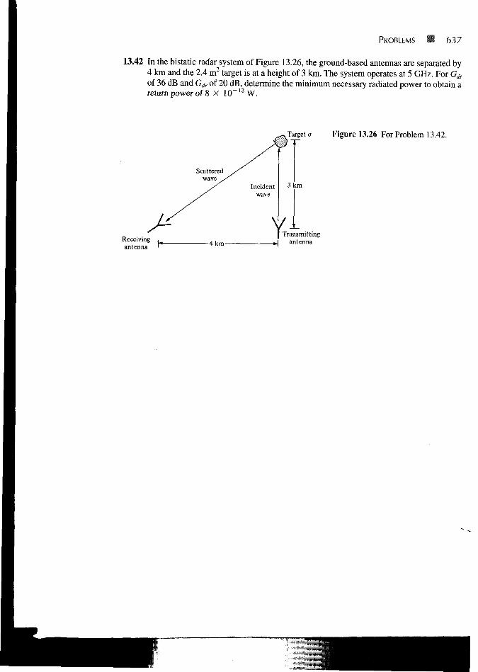
PROBLEMS 637
13.42 In the bistatic radar system of Figure 13.26, the ground-based antennas are separated by4 km and the 2.4 m2 target is at a height of 3 km. The system operates at 5 GHz. For Gdt
of 36 dB and Gdr of 20 dB, determine the minimum necessary radiated power to obtain areturn power of 8 X 10~12W.
Scatteredwave
Receivingantenna
Target a Figure 13.26 For Problem 13.42.
3 km
Transmittingantenna

Chapter 14
MODERN TOPICS
The future has several names. For the weak, it is the impossible. For the faith-hearted, it is the unknown. For the thoughtful and valiant, it is ideal.
—VICTOR HUGO
14.1 INTRODUCTION
Besides wave propagation, transmission lines, waveguides, and antennas, there are severalother areas of applications of EM. These include microwaves, electromagnetic interfer-ence and compatibility, fiber optics, satellite communication, bioelectromagnetics, electricmachines, radar meteorology, and remote sensing. Due to space limitation, we shall coverthe first three areas in this chapter: microwaves, electromagnetic interference and compat-ibility, and fiber optics. Since these topics are advanced, only an introductory treatment ofeach topic will be provided. Our discussion will involve applying the circuit conceptslearned in earlier courses and the EM concepts learned in earlier chapters.
14.2 MICROWAVES
At the moment, there are three means for carrying thousands of channels over long dis-tances: (a) microwave links, (b) coaxial cables, and (c) fiber optic, a relatively new tech-nology, to be covered later.
Microwaves arc I:M wines whose IrequiMicies rnngo from approximately .MX) M H /to I (KM) Gi l / .
For comparison, the signal from an AM radio station is about 1 MHz, while that from anFM station is about 100 MHz. The higher frequency edge of microwaves borders on theoptical spectrum. This accounts for why microwaves behave more like rays of light thanordinary radio waves. You may be familiar with microwave appliances such as the mi-crowave oven, which operates at 2.4 GHz, the satellite television, which operates at about4 GHz, and the police radar, which works at about 22 GHz.
Features that make microwaves attractive for communications include wide availablebandwidths (capacities to carry information) and directive properties of short wavelengths.Since the amount of information that can be transmitted is limited by the available band-
638

14.2 MICROWAVES • 639
width, the microwave spectrum provides more communication channels than the radio andTV bands. With the ever increasing demand for channel allocation, microwave communi-cations has become more common.
A microwave system1 normally consists of a transmitter (including a microwave os-cillator, waveguides, and a transmitting antenna) and a receiver subsystem (including a re-ceiving antenna, transmission line or waveguide, microwave amplifiers, and a receiver). Amicrowave network is usually an interconnection of various microwave components anddevices. There are several microwave components and variations of these components.Common microwave components include:
• Coaxial cables, which are transmission lines for interconnecting microwave compo-nents
• Resonantors, which are usually cavities in which EM waves are stored
• Waveguide sections, which may be straight, curved or twisted
• Antennas, which transmit or receive EM waves efficiently
• Terminators, which are designed to absorb the input power and therefore act as one-ports
• Attenuators, which are designed to absorb some of the EM power passing through itand thereby decrease the power level of the microwave signal
• Directional couplers, which consist of two waveguides and a mechanism for cou-pling signals between them
• Isolators, which allow energy flow only in one direction
• Circulators, which are designed to establish various entry/exit points where powercan either be fed or extracted
• Filters, which suppress unwanted signals and/or separate signals of different fre-quencies.
The use of microwaves has greatly expanded. Examples include telecommunications,radio astronomy, land surveying, radar, meteorology, UHF television, terrestrial mi-crowave links, solid-state devices, heating, medicine, and identification systems. We willconsider only four of these.
1. Telecommunications: (the transmission of analog or digital information from onepoint to another) is the largest application of microwave frequencies. Microwaves propa-gate along a straight line like a light ray and are not bent by the ionosphere as are lower fre-quency signals. This makes communication satellites possible. In essence, a communica-tion satellite is a microwave relay station that is used to link two or more ground-basedtransmitters and receivers. The satellite receives signals at one frequency, repeats or am-plifies it, and transmits it at another frequency. Two common modes of operation for satel-lite communication are portrayed in Figure 14.1. The satellite provides a point-to-point
'For a comprehensive treatment of microwaves, see D. M. Pozar, Microwave Engineering, NewYork, John Wiley, 2nd., 1998.

640 Modern Topics
Satellite
(a) Point-to-point link via satellite microwave
: : : , Satellite
Multiple receivers Multiple receivers
(b) Broadcast link via satellite microwave
Figure 14.1 Satellite communications configurations. Source: W. Stallings,Data and Computer Communications, 5th ed. Upper Saddle River, NJ: Pren-tice Hall, 1977, p. 90.

14.2 MICROWAVES 641
link in Figure 14.1 (a), while it is being used to provide multiple links between one ground-based transmitter and several ground-based receivers in Figure 14.1(b).
2. Radar Systems: Radar systems provided the major incentive for the developmentof microwave technology because one obtains better resolution for radar instruments athigher frequencies. Only the microwave region of the spectrum could provide the requiredresolution with antennas of reasonable size. The ability to focus a radiated wave sharply iswhat makes microwaves so useful in radar applications. Radar is used to detect aircraft,guide supersonic missiles, observe and track weather patterns, and control flight traffic atairports. It is also used in burglar alarms, garage-door openers, and police speed detectors.
3. Heating: Microwave energy is more easily directed, controlled, and concentratedthan low-frequency EM waves. Also, various atomic and molecular resonances occur atmicrowave frequencies, creating diverse application areas in basic science, remotesensing, and heating methods. The heating properties of microwave power are useful in awide variety of commercial and industrial applications. The microwave oven, shown inFigure 14.2, is a typical example. When the magnetron oscillates, microwave energy is ex-tracted from the resonant cavities. The reflections from the stationary walls and the motionof the stirring fan cause the microwave energy to be well distributed. Thus the microwaveenables the cooking process to be fast and even. Besides cooking, microwave heatingproperties are used in physical diathermy and in drying potato chips, paper, cloth, etc.
A microwave circuit consists of microwave components such as sources, transmissionlines, waveguides, attenuators, resonators, circulators, and filters. One way of analyzingsuch as a circuit is to relate the input and output variables of each component. Severalsets of parameters can be used for relating input and output variables but at high frequen-cies such as microwave frequencies where voltage and current are not well defined,S-parameters are often used to analyze microwave circuits. The scattering or ^-parametersare defined in terms of wave variables which are more easily measured at microwave fre-quencies than voltage and current.
Stirrer fan Waveguide
Metalcavity
Magnetrontube
Power supply
Figure 14.2 Microwave oven. Source: N. Schlager (ed.), How Products are Made. Detroit, MI: GaleResearch Inc., 1994, p. 289.

642 Modern Topics
Consider the two-port network shown in Figure 14.3. The traveling waves are relatedto the scattering parameters according to
b1 = Sua1 + Sna2
or in matrix form
_ \SU
\S2\
5,2S22
(14.1)
(14.2)
where ax and a2 represent the incident waves at ports 1 and 2 respectively; while b\ and b2
represent the reflected waves, as shown in Figure 14.3. For the S matrix, the off-diagonalterms represent voltage wave transmission coefficients, while the diagonal terms representreflection coefficients. If the network is reciprocal, it will have the same transmission char-acteristics in either direction, i.e.,"
If the network is symmetrical, then
= S22
For a matched two-port, the reflection coefficients are zero and
Sn =S22 = 0
(14.3)
(14.4)
(14.5)
The input reflection coefficient can be expressed in terms of the S-parameters and theload ZL as
where
_ b\ _ c ,a - S22i- L
(14.6)
(14.7)
-O-
- O
- O
b2o-
Figure 14.3 A two-port network.

14.2 MICROWAVES 643
Similarly, the output reflection coefficient (with Vg = 0) can be expressed in terms of thegenerator impedance Zg and the S-parameters as
r = a2
(14.8)vg=o
where
_zg-zo8 " zK + z o
(14.9)
EXAMPLE 14.1 The following S-parameters are obtained for a microwave transistor operating at 2.5 GHz:Su = 0.85/-300 , 512 = 0.07/56^, 521 = 1.68/120°, 5 U = O.85/-4O0. Determine theinput reflection coefficient when ZL = Zo - 75 0.
Solution:
From Eq. (14.7),
Hence, using Eq. (14.6) leads to
T, = Sn = 0.857-30°
PRACTICE EXERCISE 14.1
For an hybrid coupler, the VSWRs for the input and output ports are respectivelygiven as
1+
\S
- \S
Calculate s, and so for the following scattering matrix:
0.4 J0.6[j0.6 0.2
Answer: 2.333, 1.5

644 B Modern Topics
14.3 ELECTROMAGNETIC INTERFERENCEAND COMPATIBILITY
Every electronic device is a source of radiated electromagnetic fields called radiated emis-sions. These are often an accidental by-product of the design.
Electromagnetic interference (KMI) is the degradation in the performance of adevice clue to the fields making up the electromagnetic environment.
The electromagnetic environment consists of various apparatuses such as radio and TVbroadcast stations, radar, and navigational aids that radiate EM energy as they operate.Every electronic device is susceptible to EMI. Its influence can be seen all around us. Theresults include "ghosts" in TV picture reception, taxicab radio interference with policeradio systems, power line transient interference with personal computers, and self-oscilla-tion of a radio receiver or transmitter circuit.
Electromagnetic compatibility (liMCj is achieved when a device functions satis-factorily without introducing intolerable disturbances to the electromagnetic envi-ronment or to other devices in its neighborhood.
EMC2 is achieved when electronic devices coexist in harmony, such that each device func-tions according to its intended purpose in the presence of, and in spite of, the others. EMIis the problem that occurs when unwanted voltages or currents are present to influence theperformance of a device, while EMC is the solution to the problem. The goal of EMC is toensure system or subsystem compatibility and this is achieved by applying proven designtechniques, the use of which ensures a system relatively free of EMI problems.
EMC is a growing field because of the ever-increasing density of electronic circuits inmodern systems for computation, communication, control, etc. It is not only a concern toelectrical and computer engineers, but to automotive engineers as well. The increasing ap-plication of automotive electronic systems to improve fuel economy, reduce exhaust emis-sions, ensure vehicle safety, and provide assistance to the driver has resulted in a growingneed to ensure compatibility during normal operation. We will consider the sources andcharacteristics of EMI. Later, we will examine EMI control techniques.
A. Source and Characteristics of EMIFirst, let us classify EMI in terms of its causes and sources. The classification will facilitaterecognition of sources and assist in determining means of control. As mentioned earlier,any electronic device may be the source of EMI, although this is not the intention of the de-signer. The cause of the EMI problem may be either within the system, in which case it istermed an intrasystem problem, or from the outside, in which case it is called an intersys-
2 For an in-depth treatment of EMC, see C. R. Paul, Introduction to Electromagnetic Compatibility,New York: John Wiley, 1992.

Microwaverelay link
14.3 ELECTROMAGNETIC INTERFERENCE A N D COMPATIBILITY M 645
Aircraft
Ship
— E = Emitters of InterferenceS = Susceptible Equipment
Figure 14.4 Typical examples of intersystem EMI problems. Source: J.I.N. Violette et al, Electro-magnetic Compatibility Handbook. New York: Van Nostrand Reinhold, 1987, p. 4.
tern problem. Figure 14.4 shows intersystem EMI problems. The term "emitter" is com-monly used to denote the source of EMI, while the term "susceptor" is used to designate avictim device. Tables 14.1 and 14.2 present typical causes of both intrasystem and inter-system problems. Both intrasystem and intersystem EMI generally can be controlled bythe system design engineer by following some design guidelines and techniques. For in-
TABLE14.1 Intrasystem EMI Causes
Emitters Susceptors
Power supplies
Radar transmitters
Mobile radio transmitters
Fluorescent lights
Car ignition systems
Relays
Radar receivers
Mobile radio receivers
Ordnance
Car radio receivers

646 Modem Topics
TABLE 14.2 Intersystem EMI Causes
Emitters Susceptors
Lightning strokesComputersPower LinesRadar transmittersPolice radio transmittersFluorescent lightsAircraft transmitters
Radio receiversTV setsHeart pacers
Aircraft navigation systems
Taxicab radio receivers
Industrial controlsShip receivers
trasystem EMI problems, for example, the design engineer may apply proper groundingand wiring arrangements, shielding of circuits and devices, and filtering.
The sources of EMI can be classified as natural or artificial (man-made). The originsof EMI are basically undesired conducted emissions (voltages and/or currents) or radiatedemissions (electric and/or magnetic fields). Conducted emissions are those currents thatare carried by metallic paths (the unit's power cord) and placed on the common powernetwork where they may cause interference with other devices that are connected to thisnetwork. Radiated emissions concern the electric fields radiated by the device that may bereceived by other electronic devices causing interference in those devices. Figure 14.5 il-lustrates the conceptual difference between conducted and radiated paths.
No single operating agency has jurisdiction over all systems to dictate actions neces-sary to achieve EMC. Thus, EMC is usually achieved by industrial association, voluntaryregulation, government-enforced regulation, and negotiated agreements between the af-fected parties. Frequency plays a significant role in EMC. Frequency allocations and as-signments are made according to the constraints established by international treaties. TheRadio Regulations resulting from such international treaties are published by the Interna-
Conductedinterference
Power cables
Figure 14.5 Differences betweenconducted and radiated emissions.
14.3 ELECTROMAGNETIC INTERFERENCE A N D COMPATIBILITY 647
tional Telecommunication Union (ITU). The Federal Communications Commission (FCC)has the authority over radio and wire communications in the United States. The FCC hasset limits on the radiated and conducted emissions of electronic devices including elec-tronic typewriters, calculators, televisions, printers, modems, and personal computers. It isillegal to market an electronic device in the United States unless its radiated and conductedemissions have been measured and do not exceed the limits of FCC regulations. Therefore,any electronic device designed today that is designed without incorporating EMC designprinciples will probably fail to comply with the FCC limits.
B. EMI Control Techniques
To control or suppress EMI, the three common means employed in the design process aregrounding, shielding, and filtering. Although each technique has a distinct role in systemdesign, proper grounding may sometimes minimize the need for shielding and filtering;also proper shielding may minimize the need for filtering. Therefore, we discuss the threetechniques, grounding, shielding, and filtering in that order.
Grounding:
Grounding is the establishment of an electrically conductive path between two points toconnect electrical and electronic elements of a system to one another or to some referencepoint, which may be designated the ground. An ideal ground plane is a zero-potential,zero-impedance body that can be used as a reference for all signals in associated circuitry,and to which any undesired current can be transferred for the elimination of its effects.
The purpose of the floating ground is to isolate circuits or equipment electrically froma common ground plane. This type of grounding technique may cause a hazard. Thesingle-point grounding is used to minimize the effects of facility ground currents. Themultiple-point grounding minimizes ground lead lengths. The ground plane might be aground wire that is carried throughout the system or a large conductive body.
Bonding is the establishment of a low-impedance path between two metal surfaces.Grounding is a circuit concept, while bonding denotes the physical implementation of thatconcept. The purpose of a bond is to make a structure homogeneous with respect to theflow of electrical currents, thus avoiding the development of potentials between the metal-lic parts, since such potentials may result in EMI. Bonds provide protection from electricalshock, power circuit current return paths, and antenna ground plane connections, and alsominimize the potential difference between the devices. They have the ability to carry largefault current.
There are two types of bond: direct and indirect bonds. The direct bond is a metal-to-metal contact between the elements connected, while the indirect bond is a contact throughthe use of conductive jumpers.
The dc resistance Rdc of a bond is often used as an indication of bond quality. It isgiven by
aS(14.10)

648 Modern Topics
where € is the length of the bond, a is its conductivity, and S is its cross-sectional area. Asfrequency increases, the bond resistance increases due to skin effect. Thus the ac resistanceRac is given as
adw(14.11)
where w is the width of the bond and 5 is the skin depth.Bonding effectiveness can be expressed as the difference (in dB) between the induced
voltages on an equipment case with and without the bond trap.
Shielding:
The purpose of shielding is to confine radiated energy to a specific region or to prevent ra-diated energy from entering a specific region. Shields may be in the form of partitions andboxes as well as in the form of cable and connector shields.
Shield types include solid, nonsolid (e.g., screen), and braid, as is used on cables. Inall cases, a shield can be characterized by its shielding effectiveness. The shielding effec-tiveness (SE) is defined as
SE=.101og 10incident power density
transmitted power density(14.12)
where the incident power density is the power density at a measuring point before a shieldis installed and the transmitted power is the power density at the same point after the shieldis in place. In terms of the field strengths, the shielding effectiveness may also be definedas the ratio of the field Et transmitted through to the inside to the incident field Et. Thus, SEis given by
SE= 20 lo g l 0§ (14.13)
For magnetic fields,
SE = 20 log10Ht
(14.14)
For example, aluminum has a = 3.5 X 10⁷ S/m, e = eo, jt = /xo, an aluminum sheet at100 MHz has an SE of 100 dB at a thickness of 0.01 mm. Since an-aluminum sheet for acomputer cabinet is much thicker than this, an aluminum case is considered a highly effec-tive shield. A cabinet that effectively shields the circuits inside from external fields is alsohighly effective in preventing radiation from those circuits to the external world. Becauseof the effective shield, radiated emission from the computer system is caused by openingsin the cabinet such as cracks, holes from disc drives, etc. and from wires that penetrate thecabinet such as power cord and cables to external devices.
14.4 OPTICAL FIBER • 649
Filtering:
An electrical filter is a network of lumped or distributed constant resistors, inductors, andcapacitors that offers comparatively little opposition to certain frequencies, while blockingthe passage of other frequencies. Filter provides the means whereby levels of conductedinterference are substantially reduced.
The most significant characteristic of a filter is the insertion loss it provides as a func-tion of frequency. Insertion loss (IL) is defined as
/L = 201og 1 0 ^ (14.15)
where V1 is the output voltage of a signal source with the filter in the circuit, and V2 is theoutput voltage of the signal source without the use of the filter. Low-pass filters are com-monly used in EMC work. The insertion loss for the low-pass filters is given by
IL = 10 log10 (1 + F2) dB (14.16)
_ \irfRC, for capacitive filter\
where
k irfL/R, for inductive filter
and/is the frequency.
14.4 OPTICAL FIBER
In the mid 1970s, it was recognized that the existing copper technology would be unsuit-able for future communication networks. In view of this, the telecommunication industryinvested heavily in research into optical fibers. Optical fiber provides an attractive alterna-tive to wire transmission lines such are twisted pair and coaxial cable (or coax). Opticalfiber3 has the following advantages over copper:
• Bandwidth: It provides a very high capacity for carrying information. It has suffi-cient bandwidth that bit-serial transmission can be used, thereby considerably re-ducing the size, cost, and complexity of the hardware.
• Attenuation: It provides low attenuation and is therefore capable of transmittingover a long distance without the need of repeaters.
• Noise susceptibility: It neither radiates nor is affected by electromagnetic interfer-ence. The immunity from EMI is due to the fact that there are no metal parts so thatthere can be no conduction currents.
3 There are several excellent books that can provide further exposition on optical fiber. See, forexample, S. L. W. Meardon, The Elements of Fiber Optics, Englewood Cliffs, NJ: Regents/PrenticeHall, 1993.

650 Modern Topics
• Security: It is more secure from malicious interception because it is not easy to tapa fiber-optic cable without interrupting communication.
• Cost: The cost of optical fibers has fallen considerably over the past few years andwill continue to fall. So is the cost of related components such as optical transmit-ters and receivers.
These impressive advantages of fiber optics over electrical media have made it a populartransmission medium in recent times. Although optical fiber is more expensive and is usedmainly for point-to-point links, there has been a rapid changeover from coax and twistedpair to optical fibers for telecommunication systems, instrumentation, cable TV networks,industrial automation, and data transmission systems.
An optical fiber is a dielectric waveguide operating at optical frequency.
Optical frequencies are on the order of 100 THz. As shown in Figure 14.6, an optical fiberconsists of three concentric cylindrical sections: the core, the cladding, and the jacket. Thecore consists of one or more thin strands made of glass or plastic. The cladding is the glassor plastic coating surrounding the core, which may be step-index or graded-index. In thestep-index core, the refractive index is uniform but undergoes an abrupt change at thecore-cladding interface, while the graded-index core has a refractive index that varies withthe radial distance from the center of the fiber. The jacket surrounds one or a bundle ofcladded fibers. The jacket is made of plastic or other materials to protect against moisture,crushing, etc.
A ray of light entering the core will be internally reflected when incident in the densermedium and the angle of incidence is greater than a critical value. Thus a light ray is re-flected back into the original medium and the process is repeated as light passes down thecore. This form of propagation is multimode, referring to the variety of angles that willreflect, as shown in Figure 14.7. It causes the signal to spread out in time and limits the rate
CoreN
Jacket
4- - Cladding
Light at less thancritical angle isabsorbed in jacket
Angle ofincidence
Angle ofreflection
Figure 14.6 Optical fiber.
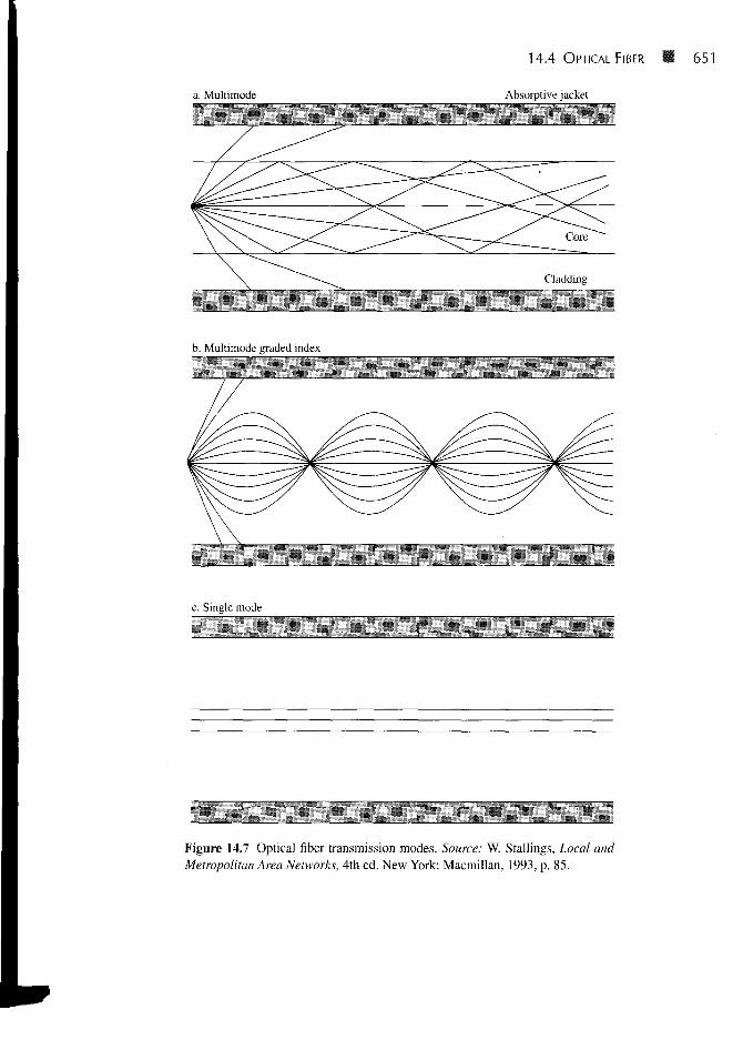
14.4 OPTICAL FIBER 651
a. Multimode Absorptive jacket
Cladding
b. Multimode graded index
c. Single mode
Figure 14.7 Optical fiber transmission modes. Source: W. Stallings, Local andMetropolitan Area Networks, 4th ed. New York: Macmillan, 1993, p. 85.

652 Modern Topics
at which data can be accurately received. By reducing the radius of the core, a single-modepropagation occurs. This eliminates distortion.
A fiber-optic system is similar to a conventional transmission system. As shown inFigure 14.8, a fiber-optic system consists of a transmitter, a transmission medium, and a re-ceiver. The transmitter accepts and converts input electrical signals in analog or digitalform to optical signals. The transmitter sends the optical signal by modulating the output ofa light source (usually an LED or a laser) by varying its intensity. The optical signal istransmitted over the optical fiber to a receiver. At the receiver, the optical signal is con-verted back into an electrical signal by a photodiode.
The performance of a fiber-optic link depends on the numerical aperture (NA), atten-uation, and dispersion characteristics of the fiber. As signals propagate through the fiber,they become distorted due to attenuation and dispersion.
Numerical Aperture:
This is the most important parameter of an optical fiber. The value of NA is dictated by therefractive indices of the core and cladding. By definition, the refractive index n of amedium is defined as
speed of light in a vacuum
speed of light in the medium1
cum
(14.18)
Since fim = /x0 in most practical cases,
n = (14.19)
indicating that the refractive index is essentially the square root of the dielectric constant.Keep in mind that er can be complex as discussed in Chapter 10. For common materials,n = 1 for air, n = 1.33 for water, and n = 1.5 for glass.
As a light ray propagates from medium 1 to medium 2, Snell's law must be satisfied.
= n2 sin (14.20)
Electrical datainput
Electrical toopticalconverter
Optical fiber cable
Transmissionmedium
Light source
Figure 14.8 A typical fiber-optic system.
Optical toelectricalconverter
Light detector
Electrical dataoutput
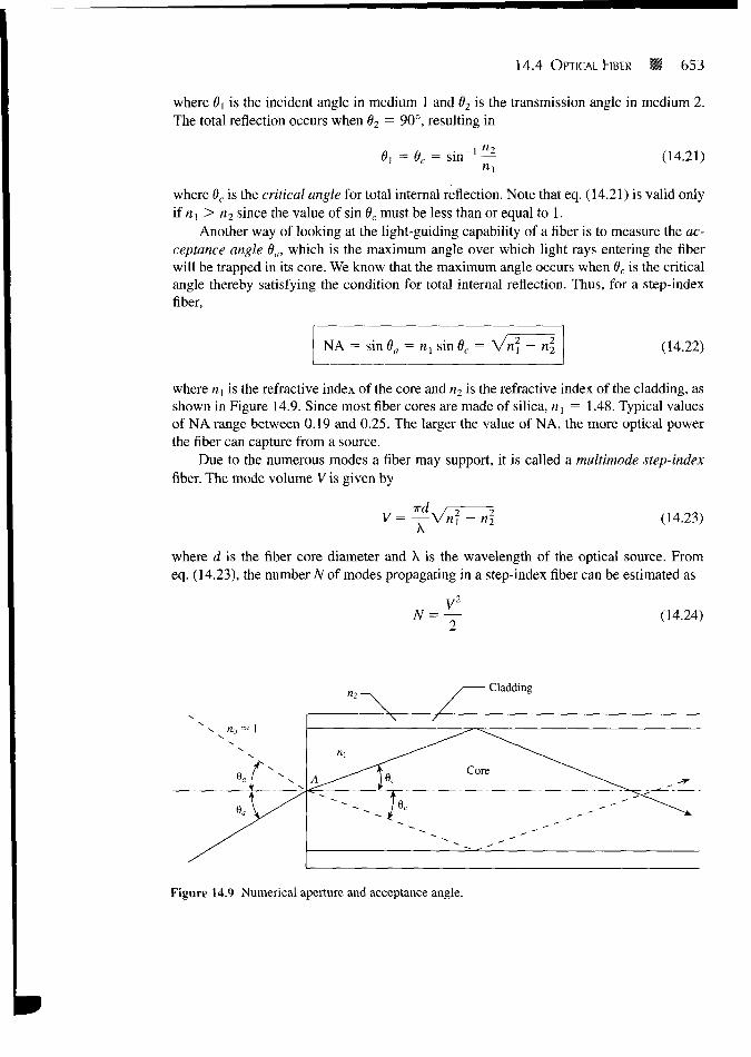
14.4 OPTICAL FIBER 653
where d\ is the incident angle in medium 1 and 92 is the transmission angle in medium 2.The total reflection occurs when 82 = 90°, resulting in
= 6C = sin"1 ^ (14.21)
where 9C is the critical angle for total internal reflection. Note that eq. (14.21) is valid onlyif n! > n2 since the value of sin 9C must be less than or equal to 1.
Another way of looking at the light-guiding capability of a fiber is to measure the ac-ceptance angle da, which is the maximum angle over which light rays entering the fiberwill be trapped in its core. We know that the maximum angle occurs when 6C is the criticalangle thereby satisfying the condition for total internal reflection. Thus, for a step-indexfiber,
NA = sin 6a = n, sin 6C = (14.22)
where «, is the refractive index of the core and n2 is the refractive index of the cladding, asshown in Figure 14.9. Since most fiber cores are made of silica, ny = 1.48. Typical valuesof NA range between 0.19 and 0.25. The larger the value of NA, the more optical powerthe fiber can capture from a source.
Due to the numerous modes a fiber may support, it is called a multimode step-indexfiber. The mode volume V is given by
V = (14.23)
where d is the fiber core diameter and A is the wavelength of the optical source. Fromeq. (14.23), the number N of modes propagating in a step-index fiber can be estimated as
N = (14.24)
• Cladding
X N « O ~ 1\ /
, ^^U Core ^""""\
Figure 14.9 Numerical aperture and acceptance angle.
L

654 Modern Topics
Attenuation:
As discussed in Chapter 10, attentuation is the reduction in the power of the optical signal.Power attenuation (or fiber loss) in an optical fiber is governed by
dz= -ccP (14.25)
where a is the attenuation and P is the optical power. In eq. (14.25), it is assumed that awave propagates along z. By solving eq. (14.25), the power P(0) at the input of the fiberand the power P(() of the light after £ are related as
P(£) = P(0)e~ (14.26)
It is customary to express attenuation a in dB/km and length I of the fiber in km. In thiscase, eq. (14.26) becomes
at = 101og10P(0)P(€)
(14.27)
Thus, the power of the light reduces by a decibels per kilometer as it propagates throughthe fiber. Equation (14.27) may be written as
P(<3>) = P(0) = 10-crf/10
For I = 100 km,
P(0) _ f 10~100 for coaxial cable/>(€) \ lO~ 2 for fiber
indicating that much more power is lost in the coaxial cable than in fiber.
(14.28)
(14.29)
Dispersion:m
This is the spreading of pulses of light as they propagate down a fiber. As the pulses repre-senting 0s spread, they overlap epochs that represent Is. If dispersion is beyond a certainlimit, it may confuse the receiver. The dispersive effects in single-mode fibers are muchsmaller than in multimode fibers.
EXAMPLE 14.2A step-index fiber has a core diameter of 80 (im, a core refractive index of 1.62, and a nu-merical aperture of 0.21. Calculate: (a) the acceptance angle, (b) the refractive index thatthe fiber can propagate at a wavelength of 0.8 fim, (c) the number of modes that the fibercan propagate at a wavelength of 0.8 /xm.

14.4 OPTICAL FIBER 655
Solution:
(a) Since sin da = NA = 0.21, then
= sin"1 0.21 = 12.12°
(b) From NA = vn\ - n\, we obtain
(c)
Hence
n2 = Vn? - NA2 = Vl .62 2 - 0.212 = 1.606
irdNAX " " ' "A X
TT(80 X 10~6) X 0.21
0.8 X 10 - 6 = 65.973
V1
N = — = 2176 modes
PRACTICE EXERCISE 14.2
A silica fiber has a refractive index of 1.48. It is surrounded by a cladding materialwith a refractive index of 1.465. Find: (a) the critical angle above which total inter-nal reflection occurs, (b) the numerical aperture of the fiber.
Answer: (a) 81.83°, (b) 0.21.
EXAMPLE 14.3 Light pulses propagate through a fiber cable with an attenuation of 0.25 dB/km. Determinethe distance through which the power of pulses is reduced by 40%.
Solution:
If the power is reduced by 40%, it means that
P(€)P(0)
Hence
= 1 - 0.4 = 0.6
1 0
10 , _L" 0.25 l 0 g l ° 0.6= 8.874 km
I

656 M Modern Topics
PRACTICE EXERCISE 14.3
A 10-km fiber with an attenuation of 0.2 dB/km serves as an optical link betweentwo cities. How much of input power is received?
Answer: 63.1%.
SUMMARY 1. Microwaves are EM waves of very short wavelengths. They propagate along a straightline like light rays and can therefore be focused easily in one direction by antennas.They are used in radar, guidance, navigation, and heating.
2. Electromagnetic compatibility (EMC) is the capability of electrical and electronicdevices to operate in their intended electromagnetic environment without suffering orcausing unacceptable degradation as a result of EMI.
3. Electromagnetic interference (EMI) is the lack of EMC. It can be suppressed bygrounding, shielding, and filtering.
4. An optical fiber is a dielectric waveguiding structure operating at optical frequenciesand it consists of a core region and a cladding region.
5. Advantages of optical fiber over copper wire include: (1) large bandwidth, (2) low at-tenuation, (3) immunity to EMI, and (4) low cost.
REVIEW QUESTIONS
14.1 Microwaves have long wavelengths.
(a) True
(b) False
14.2 The wavelength in free space of a microwave signal whose frequency is 3 GHz is:
(a) 1 mm
(b) 10 mm
(c) 10 cm
(d) l m
14.3 Which of the following is not a source of EMI?
(a) Optical fiber
(b) Personal computer
(c) Police radar
(d) Aircraft
(e) Fluorescent lamp
REVIEW QUESTIONS • 657
14.4 Optical fiber is:
(a) A transmission line
(b) A waveguide
(c) Both
14.5 Unlike coax and twisted pair, optical fibers are immune to:
(a) High-frequency transmission
(b) Signal attenuation
(c) Power loss
(d) Electromagnetic interference
14.6 As a consultant, you have been asked to design a network for an auditorium. Speed andcost are no issues. However, interference with a nearby radio station is of concern.Which of the following media could be appropriate to implement the network?
(a) Microwave
(b) Coaxial cable
(c) Fiber optic
(d) Radio
14.7 Applications of optical fiber include:
(a) Undersea cable
(b) Long-distance telecommunication
(c) High-speed data transmission
(d) Medical instrumentation
(e) All of the above
14.8 Light rays are confined within a simple optical fiber by means of:
(a) Total internal reflection at the outer edge of the cladding
(b) Total internal reflection at the core-cladding interface
(c) Reflection at the fiber's jacket
(d) Refraction
(e) Defraction
14.9 An optical fiber has a core with a refractive index of 1.45 and a cladding with a refrac-tive index of 1.42. The numerical aperture of the fiber is:
(a) 0.12
(b) 0.18
(c) 0.29
(d) 0.38

658 Modern Topics
PROBLEMS
14.10 A 20-km long fiber-optic cable has an output power of 0.02 mW. If the fiber loss is 0.48dB/km, what is the input power to the fiber?
(a) 52piW
(b) 19/xW(c) 7/xW(d) 2ftW
Answers: 14.1b, 14.2c, 14.3a, 14.4b, 14.5d, 14.6c, 14.7e, 14.8b, 14.9c, 14.10a.
14.1 Discuss briefly some applications of microwaves other than those discussed in the text.
14.2 A useful set of parameters, known as the scattering transfer parameters, is related to theincident and reflected waves as
l fr,, Ti2] \b2T2I T22\[a2
(a) Express the T-parameters in terms of the S-parameters.(b) Find T when
' 0.2 0.4S =
0.4 0.2
14.3 The S-parameters of a two-port network are:
Sn = 0.33 - jO.16, Sl2 = S21 = 0.56, S22 = 0.44 - jO.62
Find the input and output reflection coefficients when ZL = Zo = 50 Q and Zg = 2ZO.
14.4 Why can't regular lumped circuit components such as resistors, inductors, and capaci-tors be used at microwave frequencies?
14.5 In free space, a microwave signal has a frequency of 8.4 GHz. Calculate the wavelengthof the signal.
14.6 An electrostatic discharge (ESD) can be modeled as a capacitance of 125 pF charged to1500 V and discharging through a 2-km resistor. Obtain the current waveform.
*14.7 The insertion loss of a filter circuit can be calculated in terms of its A, B, C and D pa-rameters when terminated by Zg and ZL as shown in Figure 14.10. Show that
AZL + B + CZgZL + DZgIL = 20 log!
14.8 A silver rod has rectangular cross section with height 0.8 cm and width 1.2 cm. Find:
(a) The dc resistance per 1 km of the conductor
(b) The ac resistance per 1 km of the conductor at 6 MHz
14.9 The speed of light in a given medium is measured as 2.1 X 10⁸ m/s. Find its refractiveindex.

PROBLEMS 659
Figure 14.10 For Problem 14.5.
14.10 How will optical fiber be useful in EMI isolation?
14.11 A glass fiber has a core diameter of 50 ju.m, a core refractive index of 1.62, and a claddingwith a refractive index of 1.604. If light having a wavelength of 1300 nm is used, find:
(a) The numerical aperture
(b) The acceptance angle
(c) the number of transmission modes
14.12 An optical fiber with a radius of 2.5 fjm and a refractive index of 1.45 is surrounded byan air cladding. If the fiber is illuminated by a ray of 1.3 /xm light, determine:
(a) V
(b) NA
(c) An estimate of how many modes can propagate.
14.13 An optical fiber with an attenuation of 0.4 dB/km is 5 km long. The fiber has »! = 1.53,n2 = 1.45, and a diameter of 50 pm. Find:
(a) The maximum angle at which rays will enter the fiber and be trapped
(b) The percentage of input power received
14.14 A laser diode is capable of coupling 10 mW into a fiber with attenuation of 0.5 dB/km. Ifthe fiber is 850 m long, calculate the power received at the end of the fiber.
14.15 Attenuation a10 in Chapter 10 is in Np/m, whereas attenuation al4 in this chapter is indB/km. What is the relationship between the two?
14.16 A lightwave system uses a 30-km fiber link with a loss of 0.4 dB/km. If the system re-quires at least 0.2 mW at the receiver, calculate the minimum power that must belaunched into the fiber.
14.17 (a) Discuss the advantages derived from using a fiber optic cable,
(b) What is pulse dispersion?

Chapter 15
NUMERICAL METHODS
The recipe for ignorance is: be satisfied with your opinions and content with yourknowledge.
—ELBERT HUBBARD
15.1 INTRODUCTION
In the preceding chapters we considered various analytic techniques for solving EM prob-lems and obtaining solutions in closed form. A closed form solution is one in the form of anexplicit, algebraic equation in which values of the problem parameters can be substituted.Some of these analytic solutions were obtained assuming certain situations, therebymaking the solutions applicable to those idealized situations. For example, in deriving theformula for calculating the capacitance of a parallel-plate capacitor, we assumed that thefringing effect was negligible and that the separation distance was very small comparedwith the width and length of the plates. Also, our application of Laplace's equation inChapter 6 was restricted to problems with boundaries coinciding with coordinate surfaces.Analytic solutions have an inherent advantage of being exact. They also make it easy toobserve the behavior of the solution for variation in the problem parameters. However, an-alytic solutions are available only for problems with simple configurations.
When the complexities of theoretical formulas make analytic solution intractable, weresort to nonanalytic methods, which include (1) graphical methods, (2) experimentalmethods, (3) analog methods, and (4) numerical methods. Graphical, experimental, andanalog methods are applicable to solving relatively few problems. Numerical methodshave come into prominence and become more attractive with the advent of fast digitalcomputers. The three most commonly used simple numerical techniques in EM are(1) moment method, (2) finite difference method, and (3) finite element method. Most EMproblems involve either partial differential equations or integral equations. Partial differ-ential equations are usually solved using the finite difference method or the finite elementmethod; integral equations are solved conveniently using the moment method. Althoughnumerical methods give approximate solutions, the solutions are sufficiently accurate forengineering purposes. We should not get the impression that analytic techniques are out-dated because of numerical methods; rather they are complementary. As will be observedlater, every numerical method involves an analytic simplification to the point where it iseasy to apply the method.
The Matlab codes developed for computer implementation of the concepts developedin this chapter are simplified and self-explanatory for instructional purposes. The notations
660
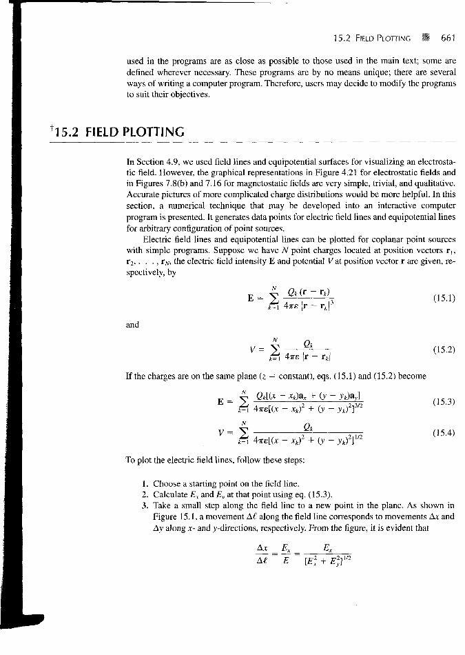
15.2 FIELD PLOTTING • 661
used in the programs are as close as possible to those used in the main text; some aredefined wherever necessary. These programs are by no means unique; there are severalways of writing a computer program. Therefore, users may decide to modify the programsto suit their objectives.
15.2 FIELD PLOTTING
In Section 4.9, we used field lines and equipotential surfaces for visualizing an electrosta-tic field. However, the graphical representations in Figure 4.21 for electrostatic fields andin Figures 7.8(b) and 7.16 for magnetostatic fields are very simple, trivial, and qualitative.Accurate pictures of more complicated charge distributions would be more helpful. In thissection, a numerical technique that may be developed into an interactive computerprogram is presented. It generates data points for electric field lines and equipotential linesfor arbitrary configuration of point sources.
Electric field lines and equipotential lines can be plotted for coplanar point sourceswith simple programs. Suppose we have N point charges located at position vectors r t,r2 , . . . , rN, the electric field intensity E and potential V at position vector r are given, re-spectively, by
y Qk(r-rk)t=i Airs \r - rk\
3(15.1)
and
ift\ 4ire |r - rk\
If the charges are on the same plane (z = constant), eqs. (15.1) and (15.2) become
N
E= 2N
k=\
- xkf + (y - ykff2
Qk
- xkfTo plot the electric field lines, follow these steps:
- ykf}}m
(15.2)
(15.3)
(15.4)
1. Choose a starting point on the field line.2. Calculate Ex and Ey at that point using eq. (15.3).3. Take a small step along the field line to a new point in the plane. As shown in
Figure 15.1, a movement A€ along the field line corresponds to movements AJC andAy along x- and y-directions, respectively. From the figure, it is evident that
Ax Ex
E [E2X
2]U2

662 Numerical Methods
field line
new point
point
Figure 15.1 A small displacement on a field line.
or
Ax = (15.5)
Similarly,
y
• Ey(15.6)
Move along the field line from the old point (x, y) to a new point x' = x + Ax,y' =y + Ay.
4. Go back to steps 2 and 3 and repeat the calculations. Continue to generate new pointsuntil a line is completed within a given range of coordinates. On completing the line,go back to step 1 and choose another starting point. Note that since there are an infi-nite number of field lines, any starting point is likely to be on a field line. The pointsgenerated can be plotted by hand or by a plotter as illustrated in Figure 15.2.
To plot the equipotential lines, follow these steps:
1. Choose a starting point.2. Calculate the electric field (Ex, Ey) at that point using eq. (15.3).
Figure 15.2 Generated points on £-field lines(shown thick) and equipotential lines (shown dotted).

15.2 FIELD PLOTTING 663
3. Move a small step along the line perpendicular to £-field line at that point. Utilizethe fact that if a line has slope m, a perpendicular line must have slope — Mm. Sincean fi-field line and an equipotential line meeting at a given point are mutually or-thogonal there,
Ax = (15.7)
Ay =+
(15.8)
Move along the equipotential line from the old point (x, y) to a new point(x + Ax, y + Ay). As a way of checking the new point, calculate the potential atthe new and old points using eq. (15.4); they must be equal because the points areon the same equipotential line.
4. Go back to steps 2 and 3 and repeat the calculations. Continue to generate newpoints until a line is completed within the given range of x and >>. After completingthe line, go back to step 1 and choose another starting point. Join the points gener-ated by hand or by a plotter as illustrated in Figure 15.2.
By following the same reasoning, the magnetic field line due to various current distri-butions can be plotted using Biot-Savart law. Programs for determining the magnetic fieldline due to line current, a current loop, a Helmholtz pair, and a solenoid can be developed.Programs for drawing the electric and magnetic field lines inside a rectangular waveguideor the power radiation pattern produced by a linear array of vertical half-wave electricdipole antennas can also be written.
EXAMPLE 15.1Write a program to plot the electric field and equipotential lines due to:
(a) Two point charges Q and —4Q located at (x, y) = ( - 1 , 0) and (1,0), respectively.
(b) Four point charges Q, -Q,Q, and - Q located at (x,y) = ( - 1 , -1 ) , (1 , -1 ) , (1, 1), and(—1, 1), respectively. Take QIAire = landA€ = 0.1. Consider the range — 5 < x , y < 5.
Solution:
Based on the steps given in Section 15.2, the program in Figure 15.3 was developed.Enough comments are inserted to make the program as self-explanatory as possible. Forexample, to use the program to generate the plot in Figure 15.4(a), load program plotit inyour Matlab directory. At the command prompt in Matlab, type
plotit ([1 - 4 ] , [-1 0; 1 0], 1, 1, 0.1, 0.01, 8, 2, 5)
where the numbers have meanings provided in the program. Further explanation of theprogram is provided in the following paragraphs.
Since the £"-field lines emanate from positive charges and terminate on negativecharges, it seems reasonable to generate starting points (xs, ys) for the £-field lines on smallcircles centered at charge locations (xQ, yQ); that is,
xs = xQ + r cos 0
y, = Vn + rsind
(15.1.1a)
(15.1.1b)

664 Numerical Methods
function plotit(charges,location,ckEField,ckEq,DLE,DLV,NLE,NLV,PTS)figure;hold on;% Program for plotting the electric field lines% and equipotential lines due to coplanar point charges% the plot is to be within the range -5<x,y<5%% This is the correct usage:% function plotit(charges, location,ckEField,ckEq,DLE,DLV,NLE,NLV,PTS)%% where,% charges = a vector containing the charges% location = a matrix where each row is a charge location% ckEField = Flag set to 1 plots the Efield lines% ckEq = Flag set to 1 plots the Equipotential lines% DLE or DLV = the increment along E & V lines% NLE = No. of E-Field lines per charge% NLV = No. of Equipotential lines per charge% PTS => Plots every PTS point (i.e. if PTS = 5 then plotevery 5th point)% note that constant Q/4*Pie*ErR is set equal to 1.0
% Determine the E-Field Lines% For convenience, the starting pointsdistributed about charge locationsQ=charges;XQ = location(:,1);YQ = location):,2);JJ=1;NQ = length(charges);if (ckEField)for K=1:NQ
for I =1:NLETHETA = 2*pi*(1-1)/(NLE);
(XS,YS) are radially
XS=XQ(K) +YS=YQ(K) +XE=XS;YE=YS;JJ=JJ+1;if (~mod(JJ
plot (XEendwhile(1)
0.1*cos0.1*sin
,PTS)), YE) ;
% Find i ncrementEX=0;EY=0;
(THETA);(THETA);
and new point (X,Y)
Figure 15.3 Computer program for Example 15.1.
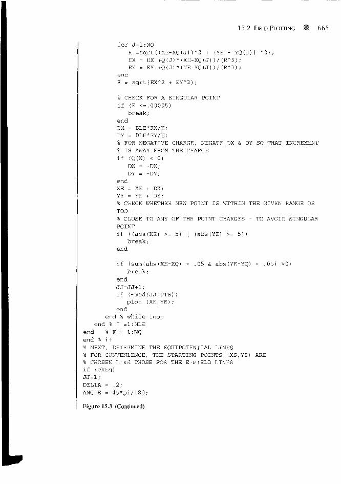
15.2 FIELD PLOTTING 665
for J=1:NQR =sqrt((XE-XQ(J))~2 + (YE - YQ(J)) A 2 ) ;EX = EX +Q(J)*(XE-XQ(J) ) / (FT3) ;EY = EY +Q(J)*(YE-YQ(J))/(RA3);
endE = sqrt(EX^2 + EYA2);
% CHECK FOR A SINGULAR POINTif (E <=.00005)
break;endDX = DLE*EX/E;DY = DLE*EY/E;% FOR NEGATIVE CHARGE, NEGATE DX & DY SO THAT INCREMENT% IS AWAY FROM THE CHARGEif (Q(K) < 0)
DX = -DX;DY = -DY;
endXE = XE + DX;YE = YE + DY;% CHECK WHETHER NEW POINT IS WITHIN THE GIVEN RANGE ORTOO% CLOSE TO ANY OF THE POINT CHARGES - TO AVOID SINGULARPOINTif ((abs(XE) >= 5) | (abs(YE) >= 5))
break;end
if (sum(abs(XE-XQ) < .05 & abs(YE-YQ) < .05) >0)break;
endJJ=JJ+1;if (~mod(JJ,PTS))
plot (XE,YE);end
end % while loopend % I =1:NLE
end % K = 1:NQend % if% NEXT, DETERMINE THE EQUIPOTENTIAL LINES% FOR CONVENIENCE, THE STARTING POINTS (XS,YS) ARE% CHOSEN LIKE THOSE FOR THE E-FIELD LINESif (ckEq)JJ=1;DELTA = .2;ANGLE = 45*pi/180;
Figure 15.3 (Continued)

666 Numerical Methods
for K =1:NQFACTOR = .5;for KK = 1:NLVXS = XQ(K) + FACTOR*cos(ANGLE);YS = YQ(K) + FACTOR*sin(ANGLE);if ( abs(XS) >= 5 | abs(YS) >=5)
break;endDIR = 1;XV = XS;YV = YS;JJ=JJ+1;if (~mod(JJ,PTS))
plot(XV,YV);end
% FIND INCREMENT AND NEW POINT (XV,YV)N=l;while (1)
EX = 0;EY = 0;for J = 1:NQ
R = sqrt((XV-XQ(J))"2 + (YV-YQ(J))^2);EX = EX + Q(J)*(XV-XQ(J))/(RA3);EY = EY + Q(J)*(YV-YQ(J))/(R"3);
endE=sqrt(EXA2 + EY~2);if (E <= .00005)
FACTOR = 2 *FACTOR;break;
endDX = -DLV*EY/E;DY = DLV*EV/E;XV = XV + DIR*DX;YV = YV + DIR*DY;% CHECK IF THE EQUIPOTENTIAL LINE LOOPS BACK TO (X,YS)R0 = sqrt((XV - XS)"2 + (YV - YS)^2);if (R0 < DELTA & N < 50)
FACTOR = 2 *FACTOR;break;
end% CHECK WHETHER NEW POINT IS WITHIN THE GIVEN RANGE% IF FOUND OUT OF RANGE, GO BACK TO THE STARTING POINT% (S,YS)BUT INCREMENT IN THE OPPOSITE DIRECTIONif (abs(XV) > 5 | abs(YV) > 5)
DIR = DIR -2;XV = XS;YV = YS;
Figure 15.3 (Continued)

15.2 FIELD PLOTTING m 667
i f (abs(DlR) > 1)FACTOR = 2 *FACTOR;break;
endelse
if (sumfabs(XV-XQ) < .005 & abs(YV-YQ) < .005) >0)break;
endendJJ=JJ+1;if (~mod(JJ,PTS))
N=N+1;plot(XV,YV);
endend % WHILE loop
end % KKend % K
end % if
Figure 15.3 (Continued)
where r is the radius of the small circle (e.g., r = 0.1 or 0.05), and 6 is a prescribed anglechosen for each £-field line. The starting points for the equipotential lines can be generatedin different ways: along the x- and y-axes, along line y = x, and so on. However, to makethe program as general as possible, the starting points should depend on the charge loca-tions like those for the £-field lines. They could be chosen using eq. (15.1.1) but with fixed0(e.g., 45°) and variable r (e.g., 0.5, 1.0, 2.0,. . .).
The value of incremental length A€ is crucial for accurate plots. Although the smallerthe value of A€, the more accurate the plots, we must keep in mind that the smaller thevalue of A€, the more points we generate and memory storage may be a problem. Forexample, a line may consist of more than 1000 generated points. In view of the largenumber of points to be plotted, the points are usually stored in a data file and a graphicsroutine is used to plot the data.
For both the .E-field and equipotential lines, different checks are inserted in theprogram in Figure 15.3:
(a) Check for singular point (E = 0?)
(b) Check whether the point generated is too close to a charge location.
(c) Check whether the point is within the given range of —5 < x,y < 5.
(d) Check whether the (equipotential) line loops back to the starting point.
The plot of the points generated for the cases of two point charges and four pointcharges are shown in Figure 15.4(a) and (b), respectively.
668 Numerical Methods
Figure 15.4 For Example 15.1; plots of £-field lines and equipoten-tial lines due to (a) two point charges, and (b) four point charges(a two-dimensional quadrupole).
PRACTICE EXERCISE 15.1
Write a complete program for plotting the electric field lines and equipotential linesdue to coplanar point charges. Run the program for iV = 3; that is, there are threepoint charges -Q, +Q, and -Q located at (x,y) = ( -1 ,0) , (0, 1), and (1,0) re-spectively. Take Q/4irs = 1, A€ = 0.1 or 0.01 for greater accuracy and limit yourplot to - 5 S j t , y < 5.
Answer: See Figure 15.5.

15.3 THE FINITE DIFFERENCE METHOD 669
Figure 15.5 For Practice Exercise 15.1.
15.3 THE FINITE DIFFERENCE METHOD
The finite difference method1 (FDM) is a simple numerical technique used in solving prob-lems like those solved analytically in Chapter 6. A problem is uniquely defined by threethings:
1. A partial differential equation such as Laplace's or Poisson's equations2. A solution region3. Boundary and/or initial conditions
A finite difference solution to Poisson's or Laplace's equation, for example, proceeds inthree steps: (1) dividing the solution region into a grid of nodes, (2) approximating the dif-ferential equation and boundary conditions by a set of linear algebraic equations (calleddifference equations) on grid points within the solution region, and (3) solving this set ofalgebraic equations.
'For an extensive treatment of the finite difference method, see G. D. Smith, Numerical Solution ofPartial Differential Equations: Finite Difference Methods, 2nd edition. Oxford: Clarendon, 1978.
L

670 Numerical Methods
Step 1: Suppose we intend to apply the finite difference method to determine the elec-tric potential in a region shown in Figure 15.6(a). The solution region is divided into rec-tangular meshes with grid points or nodes as in Figure 15.6(a). A node on the boundaryof the region where the potential is specified is called a fixed node (fixed by the problem)and interior points in the region are called free points (free in that the potential isunknown).
Step 2: Our objective is to obtain the finite difference approximation to Poisson'sequation and use this to determine the potentials at all the free points. We recall thatPoisson's equation is given by
(15.9a)
For two-dimensional solution region such as in Figure 15.6(a), pv is replaced by ps,
T = 0, sod2V
dz
d2v d2vdx2 dy2
From the definition of the derivative of V(x, y) at point (x0, yo),
V =dVdx
V(xo + Ax, yo) - V(xo - Ax, yo)2Ax
2 Ax
(15.9b)
(15.10)
yo + A v
/ 1
h K,
(b)
Figure 15.6 Finite difference solution pattern: (a) division of the solutioninto grid points, (b) finite difference five-node molecule.

15.3 THE FINITE DIFFERENCE METHOD 671
where Ax is a sufficiently small increment along x. For the second derivative, which is thederivative of the first derivative V,
V" =dx2
dV ^ V'(xo + Ax/2,vo) - V'(xo - Ax/2,yo)
dx AxV(xo + Ax,y0) - 2V(xo,yo) + V(x0 - Ax,y0)
Vi+lJ - 2VU
(Ax)1
7
i-U
(Ax)2(15.11)
Equations (15.10) and (15.11) are the finite difference approximations for the first andsecond partial derivatives of V with respect to x, evaluated at x = xo. The approximation ineq. (15.10) is associated with an error of the order of the Ax while that of eq. (15.11) has anassociated error on the order of (Ax)2. Similarly,
V(xo,yo + Ay) - 2V(xo, yo) + V(xo,yo - Ay)d2V
dyz (AyfViJ+l -
(Ay)2(15.12)
Substituting eqs. (15.11) and (15.12) into eq. (15.9b) and letting Ax = Ay = h gives
VilJ
V,_w + ViJ+l
or
(15.13)
where h is called the mesh size. Equation (15.13) is the finite difference approximation toPoisson's equation. If the solution region is charge-free (ps = 0), eq. (15.9) becomesLaplace's equation:
dx2 dy2(15.14)
The finite difference approximation to this equation is obtained from eq. (15.13) by settingps = 0; that is
1
4ViJ+l + Vu-i) (15.15)
This equation is essentially a five-node finite difference approximation for the potential atthe central point of a square mesh. Figure 15.6(b) illustrates what is called the finite differ-
672 Numerical Methods
ence five-node molecule. The molecule in Figure 15.6(b) is taken out of Figure 15.6(a).Thus eq. (15.15) applied to the molecule becomes
V4) (15.16)
This equation clearly shows the average-value property of Laplace's equation. In otherwords, Laplace's equation can be interpreted as a differential means of stating the fact thatthe potential at a specific point is the average of the potentials at the neighboring points.
Step 3: To apply eq. (15.16) [or eq. (15.13)] to a given problem, one of the followingtwo methods is commonly used:
A. Iteration Method
We start by setting initial values of the potentials at the free nodes equal to zero or to anyreasonable guessed value. Keeping the potentials at the fixed nodes unchanged at all times,we apply eq. (15.16) to every free node in turn until the potentials at all free nodes are cal-culated. The potentials obtained at the end of this first iteration are not accurate but just ap-proximate. To increase the accuracy of the potentials, we repeat the calculation at everyfree node using old values to determine new ones. The iterative or repeated modification ofthe potential at each free node is continued until a prescribed degree of accuracy isachieved or until the old and the new values at each node are satisfactorily close.
B. Band Matrix Method
Equation (15.16) applied to all free nodes results in a set of simultaneous equations of theform
[A] [V] = [B] (15.17)
where [A] is a sparse matrix (i.e., one having many zero terms), [V] consists of theunknown potentials at the free nodes, and [B] is another column matrix formed by theknown potentials at the fixed nodes. Matrix [A] is also banded in that its nonzero termsappear clustered near the main diagonal because only nearest neighboring nodes affect thepotential at each node. The sparse, band matrix is easily inverted to determine [V\. Thus weobtain the potentials at the free nodes from matrix [V\ as
[V] = [B] (15.18)
The finite difference method can be applied to solve time-varying problems. Forexample, consider the one-dimensional wave equation of eq. (10.1), namely
d2<p
dt2 (15.19)

15.3 THE FINITE DIFFERENCE METHOD 673
where u is the wave velocity and <P is the E- or //-field component of the EM wave. Thedifference approximations of the derivatives at (xo, to) or O',y')th node shown in Figure 15.7
are
dx'
dt2
(Ax)2
<*v. -(At)2
Inserting eqs. (15.20) and (15.21) in eq. (15.20) and solving for 4>iJ+i gives
2(1 - a) <PtJ - * w _ !
where
a =u At
Ax
(15.20)
(15.21)
(15.22)
(15.23)
It can be shown that for the solution in eq. (15.22) to be stable, a £ 1. To start the finitedifference algorithm in eq. (15.22), we use the initial conditions. We assume that at t = 0,d<t>ifi/dt = 0 and use (central) difference approximation (see Review Question 15.2) toget
i JL -X. JL
ili = 0dt 2At
or
(15.24)
Substituting eq. (15.24) into eq. (15.22) and taking j = 0 (t = 0), we obtain
,,o + *,-+i.o) + 2(1 - a)*,-i0 - <PiA
r,, + At. /+ 1
?„ - A i. i - 1
/„ 2A/ . / - 2 _
Figure 15.7 Finite difference solution patternfor wave equation.
/ • 2 / - I / / + 1 / + 2
A-,, - 2A.v vu - A.v xo x,, + A x x,, + 2A.v
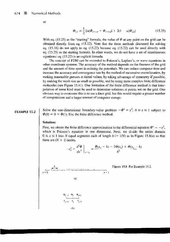
674 Numerical Methods
or
*;,i ~ ^ [«(^;-i,o + *i+i,o) + 2(1 - a)$,-j0] (15.25)
With eq. (15.25) as the "starting" formula, the value of 4> at any point on the grid can beobtained directly from eq. (15.22). Note that the three methods discussed for solvingeq. (15.16) do not apply to eq. (15.22) because eq. (15.22) can be used directly witheq. (15.25) as the starting formula. In other words, we do not have a set of simultaneousequations; eq. (15.22) is an explicit formula.
The concept of FDM can be extended to Poisson's, Laplace's, or wave equations inother coordinate systems. The accuracy of the method depends on the fineness of the gridand the amount of time spent in refining the potentials. We can reduce computer time andincrease the accuracy and convergence rate by the method of successive overrelaxation, bymaking reasonable guesses at initial values, by taking advantage of symmetry if possible,by making the mesh size as small as possible, and by using more complex finite differencemolecules (see Figure 15.41). One limitation of the finite difference method is that inter-polation of some kind must be used to determine solutions at points not on the grid. Oneobvious way to overcome this is to use a finer grid, but this would require a greater numberof computations and a larger amount of computer storage.
EXAMPLE 15.2 Solve the one-dimensional boundary-value problem —<P" = x2, 0 < x ^ 1 subject to<P(0) = 0 = <P(l). Use the finite difference method.
Solution:
First, we obtain the finite difference approximation to the differential equation <P" = —x2,which is Poisson's equation in one dimension. Next, we divide the entire domain0 < x < 1 into N equal segments each of length h (= I/A/) as in Figure 15.8(a) so thatthere are (N + 1) nodes.
d2<i>
dx2
<P(xo ~ 2<P(xo) + <P(xo - h)
h
Figure 15.8 For Example 15.2.
x= 1
(a)
l * /
(b)
15.3 THE FINITE DIFFERENCE METHOD 675
or
Thus
or
- r 2 =A ;
- 2<Pj
h
~2<P = -x2h2 -
_ l 2 2
2
Using this finite difference scheme, we obtain an approximate solution for various valuesof N. The Matlab code is shown in Figure 15.9. The number of iterations NI depends on thedegree of accuracy desired. For a one-dimensional problem such as this, NI = 50 maysuffice. For two- or three-dimensional problems, larger values of NI would be required (seeTable 15.1). It should be noted that the values of <P at end points (fixed nodes) are heldfixed. The solutions for N = 4 and 10 are shown in Figure 15.10.
We may compare this with the exact solution obtained as follows. Given thatd2(P/dx2 = ~x2, integrating twice gives
<P = + Ax + B12
% ONE-DIMENSIONAL PROBLEM OF EXAMPLE 15.2% SOLVED USING FINITE DIFFERENCE METHOD%% h = MESH SIZE% ni = NO. OF ITERATIONS DESIRED
P = [ ] ;n=2 0;ni=1000;1=1.0;h = 1/n;phi=zeros(n+1,1);x=h*[0:n]';xl=x(2:n);for k=l:ni
phi ( [2 :n] ) = [phi (3 :n+l) +phi (l:n-l) +xl.'N2*h"2] /2;end% CALCULATE THE EXACT VALUE ALSOphiex=x.*(1.0-x.A3)/12.0;diary a:test.out[[l:n+l]' phi phiex]diary off
Figure 15.9 Computer program for Example 15.2.
L

676 Numerical Methods
.05 -
.04 -
1 . 0 3 -
.02 -
.01 -
1 1
1 1
_
f 1 1 1 1
\
\ \
\ \
\
I i i i \.1 .2 .3 .4 .5 .6 .7 .9 1
Figure 15.10 For Example 15.2: plot of <P(x). Continuous curve is foriV = 10; dashed curve is for N = 4.
where A and B are integration constants. From the boundary conditions,
= 0 - > 5 = 0
1 1or A = —0(1) = 0 - > 0 = + A
Hence, the exact solution is <P = x(l — x3)/12, which is calculated in Figure 15.9 andfound to be very close to case N = 10.
PRACTICE EXERCISE 15.2
Solve the differential equation d2yldx2 + y = 0 with the boundary conditionsy(0) = 0, y(l) = 1 using the finite difference method. Take Ax = 1/4.
Answer: Compare your result with the exact solution y(x) = —sin(;c)
sin(l)
EXAMPLE 15.3Determine the potential at the free nodes in the potential system of Figure 15.11 using thefinite difference method.
Solution:
This problem will be solved using the iteration method and band matrix method.

2.5 m
20 V
/
ov
1
2
3
4
5
6
7
8
15.3 THE FINITE DIFFERENCE METHOD
Figurel5.il For Example 15.3.
677
, 3 0 V
Method 1 (Iteration Method): We first set the initial values of the potential at the freenodes equal to zero. We apply eq. (15.16) to each free node using the newest surroundingpotentials each time the potential at that node is calculated. For the first iteration:
Vl = 1/4(0 + 20 + 0 + 0) = 5
V2 = 1/4(5 + 0 + 0 + 0) = 1.25
V3 = 1/4(5 + 20 + 0 + 0) = 6.25
V4 = 1/4(1.25 + 6.25 + 0 + 0) = 1.875
and so on. To avoid confusion, each time a new value at a free node is calculated, we crossout the old value as shown in Figure 15.12. After V8 is calculated, we start the second iter-ation at node 1:
Vx = 1/4(0 + 20 + 1.25 + 6.25) = 6.875
V2 = 1/4(6.875 + 0 + 0 + 1.875) = 2.187
and so on. If this process is continued, we obtain the uncrossed values shown in Figure15.12 after five iterations. After 10 iterations (not shown in Figure 15.12), we obtain
V{ = 10.04, V2 = 4.956, V3 = 15.22, V4 = 9.786
V5 = 21.05, V6 = 18.97, V7 = 15.06, V8 = 11.26
Method 2 (Band Matrix Method): This method reveals the sparse structure of theproblem. We apply eq. (15.16) to each free node and keep the known terms (prescribed po-tentials at the fixed nodes) on the right side while the unknown terms (potentials at freenodes) are on the left side of the resulting system of simultaneous equations, which will beexpressed in matrix form as [A] [V] = [B].For node 1,
-4V, + V2 + V3 = - 2 0 - 0

678 H Numerical Methods
O s
Ox
Ox
9.659-9rh5T-%fTT-6r875"
-fr
4.705
-e-
20
0
14.85
4*T>9"
-e-
9.545
^ ~
-fr
20
20.87
-e-
18.84
-+fctr
-fr-
15.02
~T4. OO
11.25
4*09"-e—
20
-30
-30
-30
-30
15
Figure 15.12 For Example 15.3; the values not crossed out are the solutionsafter five iterations.
For node 2,
For node 3,
For node 4,
For node 5,
V, + 4V, + V4 = - 0 - 0
j - 4V3 + V4 + V5 = - 2 0
v3 - 4V4 + y6 = - o
V3 - 4V5 + Vb = - 2 0 - 30

15.3 THE FINITE DIFFERENCE METHOD 679
For node 6,
For node 7,
For node 8,
V4 + V5 - 4V6 + V7 = - 3 0
V6 - 4V7 + Vs = - 3 0 - 0
V7 - 4V8 = - 0 - 0 - 30
Note that we have five terms at each node since we are using a five-node molecule. Theeight equations obtained are put in matrix form as:
•-4• 1' . 1
6'0000
I- 4
0• .1
0000
10
- 41
• . 1
<y00
0i'I401
6'0
0' • 0
r0- 4
i
• o0"
00
• . 0
1 •
1- 4
1• 0
000
• Po' •1
- 41
0000
.0
6:r
- 4 -
v2v3v4v5V6
v7vs
- 2 00
- 2 00
- 5 0- 3 0- 3 0- 3 0
or
[A] [V] = [B]
where [A] is the band, sparse matrix, [V] is the column matrix consisting of the unknownpotentials at the free nodes, and [6] is the column matrix formed by the potential at thefixed nodes. The "band" nature of [A] is shown by the dotted loop.
Notice that matrix [A] could have been obtained directly from Figure 15.11 withoutwriting down eq. (15.16) at each free node. To do this, we simply set the diagonal (or self)terms A,, = —4 and set Atj = lifi and 7 nodes are connected or Atj = 0 if i andj nodes arenot directly connected. For example, A23 = A32 = 0 because nodes 2 and 3 are not con-nected whereas A46 = A64 = 1 because nodes 4 and 6 are connected. Similarly, matrix [B]is obtained directly from Figure 15.11 by setting Bt equal to minus the sum of the potentialsat fixed nodes connected to node i. For example, B5 = —(20 + 30) because node 5 is con-nected to two fixed nodes with potentials 20 V and 30 V. If node i is not connected to anyfixed node, B, = 0.
By inverting matrix [A] using Matlab, we obtain
M = [AV1 [B]
or
V, = 10.04, V2 = 4.958, V3 = 15.22, V4 = 9.788
V5 = 21.05, V6 = 18.97, V7 = 15.06, V8 = 11.26
which compares well with the result obtained using the iteration method.
680 I I Numerical Methods
Figure 15.13 For Practice Exercise 15.3.
50 V
PRACTICE EXERCISE 15.3
Use the iteration method to find the finite difference approximation to the potentialsat points a and b of the system in Figure 15.13.
Answer: Va = 10.01 V, Vb = 28.3 V.
EXAMPLE 15.4 Obtain the solution of Laplace's equation for an infinitely long trough whose rectangularcross section is shown in Figure 15.14. Let V) = 10 V, V2 = 100 V, V3 = 40 V, andV4 = 0 V.
Solution:
We shall solve this problem using the iteration method. In this case, the solution region hasa regular boundary. We can easily write a program to determine the potentials at the gridpoints within the trough. We divide the region into square meshes. If we decide to use a15 X 10 grid, the number of grid points along x is 15 + 1 = 16 and the number of gridpoints along y is 10 + 1 = 11. The mesh size h = 1.5/15 = 0.1 m.The 15 X 10 grid is il-
Figure 15.14 For Example 15.4.
1.0m
V, = 0 V K, = 100 V
Vl = 10 V1.5 m

(0,
"(8, 10)
1
15.3 THE FINITE DIFFERENCE METHOD • 681
Figure 15.15 For Example 15.4; a 15 X 10t(»5, 10) grid.
(8,0)•(15,0)
lustrated in Figure 15.15. The grid points are numbered (/,/) starting from the lower left-hand corner of the trough. Applying eq. (15.15) and using the iteration method, the com-puter program in Figure 15.16 was developed to determine the potential at the freenodes. At points (x,y) = (0.5, 0.5), (0.8, 0.8), (1.0, 0.5), and (0.8, 0.2) corresponding to(ij) = (5, 5), (8, 8), (10, 5), and (8, 2), respectively, the potentials after 50, 100, and 200iterations are shown in Table 15.1. The exact values (see Problem 6.18(c)), obtained usingthe method of separation of variables and a program similar to that of Figure 6.11, are alsoshown. It should be noted that the degree of accuracy depends on the mesh size h. It isalways desirable to make h as small as possible. Also note that the potentials at the fixednodes are held constant throughout the calculations.
% USING FINITE DIFFERENCE (ITERATION) METHOD% THIS PROGRAM SOLVES THE TWO-DIMENSIONAL BOUNDARY-VALUE% PROBLEM (LAPLACE'S EQUATION) SHOWN IN FIG. 15.14.% ni = NO. OF ITERATIONS% nx = NO. OF X GRID POINTS% ny = NO. OF Y GRID POINTS% v(i,j) = POTENTIAL AT GRID POINT (i,j) OR (x,y) WITH% NODE NUMBERING STARTING FROM THE LOWER LEFT-HAND% CORNER OF THE TROUGH
vl = 10.0;v2 = 100.0;v3 = 40.0;v4 = 0.0;ni = 2 00;nx = 16;ny = 11;% SET INITIAL VALUES EQUAL TO ZEROESv = zeros(nx,ny);% FIX POTENTIALS ARE FIXED NODES
Figure 15.16 Computer Program for Example 15.4.

682 Numerical Methods
for i=2:nx-l
v ( i,1) = vl;
v ( i , ny) = v3 ;
end
for j=2:ny-l
v(1,j) = v4;
v(nx,j) = v2;
end
v(l,1) = 0.5*(vl + v4);
v(nx,1) = 0.5*(vl + v2);
v(l,ny) = 0.5*(v3 + v 4 ) ;
v(nx,ny) = 0.5*(v2 + v3);
% NOW FIND v(i,j) USING EQ. (15.15) AFTER ni ITERATIONS
for k=l:ni
for i = 2:nx-l
for j=2:ny-l
v(i,j) = 0.25*( v(i+l,j)
end
end
end
diary a:testl.out
[v(6,6), v(9,9), v(ll,6), v(9,3)]
[ [l:nx, l:ny] v(i,j) ]
diary off
Figure 15.16 (Continued)
TABLE 15.1 Solution of Example 15.4 (Iteration
Method) at Selected Points
Coordinates(*,y)
(0.5, 0.5)(0.8, 0.8)(1.0,0.5)(0.8, 0.2)
Number of Iterations
50
20.9137.741.8319.87
100
22.4438.5643.1820.94
200
22.4938.5943.220.97
Exact Value
22.4438.5543.2220.89
PRACTICE EXERCISE 15.4
Consider the trough of Figure 15.17. Use a five-node finite difference scheme to find
the potential at the center of the trough using (a) a 4 X 8 grid, and (b) a 12 X 24
grid.
Answer: (a) 23.8 V, (b) 23.89 V.
60 V
50 V
15.4 THE MOMENT METHOD
Figure 15.17 For Practice Exercise 15.4.
683
15.4 THE MOMENT METHOD
Like the finite difference method, the moment method2 or the method of moments (MOM)has the advantage of being conceptually simple. While the finite difference method is usedin solving differential equations, the moment method is commonly used in solving integralequations.
For example, suppose we want to apply the moment method to solve Poisson's equa-tion in eq. (15.9a). It can be shown that an integral solution to Poisson's equation is
V =Alter
(15.26)
We recall from Chapter 4 that eq. (15.26) can be derived from Coulomb's law. We alsorecall that given the charge distribution pv(x, y, z), we can always find the potentialV(x, y, z), the electric field E(x, y, z), and the total charge Q. If, on the other hand, the po-tential V is known and the charge distribution is unknown, how do we determine pv fromeq. (15.26)? In that situation, eq. (15.26) becomes what is called an integral equation.
An integral equation is one involving ihc unknown function under the inloiiral sign.
It has the general form of
V(x) = K(x, t) p{t) dt (15.27)
where the functions K(x, i) and V(t) and the limits a and b are known. The unknown func-tion p(t) is to be determined; the function K(x, t) is called the kernel of the equation. The
2The term "moment method" was first used in Western literature by Harrington. For further exposi-tion on the method, see R. F. Harrington, Field Computation by Moment Methods. Malabar, FL:Krieger, 1968.
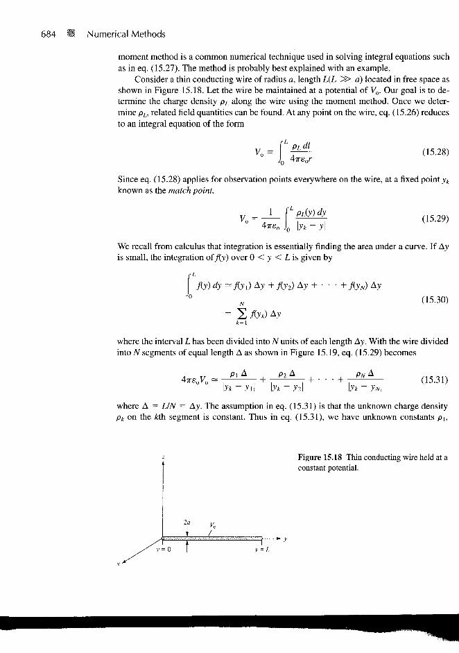
684 Numerical Methods
moment method is a common numerical technique used in solving integral equations suchas in eq. (15.27). The method is probably best explained with an example.
Consider a thin conducting wire of radius a, length L(L S> a) located in free space asshown in Figure 15.18. Let the wire be maintained at a potential of Vo. Our goal is to de-termine the charge density pL along the wire using the moment method. Once we deter-mine pL, related field quantities can be found. At any point on the wire, eq. (15.26) reducesto an integral equation of the form
Vn =L PLdl
, 4?reor(15.28)
Since eq. (15.28) applies for observation points everywhere on the wire, at a fixed point yk
known as the match point.
L PLJy) dy
*J0 \yk-y\(15.29)
We recall from calculus that integration is essentially finding the area under a curve. If Ayis small, the integration of fly) over 0 < y < L is given by
fly) dy^flyl)Ay+ f(y2) Ay + • • • + f(yN) Ay(15.30)
fly 0k=l
where the interval L has been divided into N units of each length Ay. With the wire dividedinto N segments of equal length A as shown in Figure 15.19, eq. (15.29) becomes
A 1/ Pi A
4irsoVo =\yk-yu
(15.31)
where A = LIN — Ay. The assumption in eq. (15.31) is that the unknown charge densitypk on the kth segment is constant. Thus in eq. (15.31), we have unknown constants pu
la
Figure 15.18 Thin conducting wire held at aconstant potential.

15.4 THE MOMENT METHOD • 685
pN Figure 15.19 Division of the wire into N segments.
Pi
Pk
p2, . . ., pN. Since eq. (15.31) must hold at all points on the wire, we obtain N similar
equations by choosing N match points at yu y2, • • ., y*, • • • ys o n t n e w i r e - Thus we
obtain
. . . P\ A4TT£OVO = +
4ireoVo =
+ ;-yi\ \y\ -
Pi7
+
P2A+ -, 7 +
(15.32a)
(15.32b)
4TTSOVO =Pi A Pi A
\yN-y\\• +
\yN -(15.32c)
The idea of matching the left-hand side of eq. (15.29) with the right-hand side of the equa-tion at the match points is similar to the concept of taking moments in mechanics. Here liesthe reason this technique is called moment method. Notice from Figure 15.19 that thematch points yu y2,. . .,yN are placed at the center of each segment. Equation (15.32) canbe put in matrix form as
[B] = [A] [p] (15.33)
where
[B] = 4TTSOVO(15.34)

686 Numerical Methods
[A] =
An A12A2 1 A 2 2
"IN
A-2N
(15.35a)
ym - y,
Pi
PN
m + n (15.35b)
(15.36)
In eq. (15.33), [p] is the matrix whose elements are unknown. We can determine [p] fromeq. (15.33) using Cramer's rule, matrix inversion, or Gaussian elimination technique.Using matrix inversion,
[p] = [A]"1 [B] (15.37)
where [A] is the inverse of matrix [A]. In evaluating the diagonal elements (or self terms)of matrix [A] in eq. (15.32) or (15.35), caution must be exercised. Since the wire is con-ducting, a surface charge density ps is expected over the wire surface. Hence at the centerof each segment,
V (center) =2x /-A/2
psa d<p ay
2-iraps
4TTSO
InA/2 + [(A/2)2 + a2]m
-A/2 + [(A/2)2 + a2]"2
Assuming A ^> a,
4Treo
(15.38)
where pL = 2TT aps. Thus, the self terms (m = n) are
= 21n |Aa
(15.39)

15.4 THE MOMENT METHOD • 687
Equation (15.33) now becomes
2 In ( -
\yi ~y\\2 l n ( —
Pi
P2
P/V
= 4ITP V
11
1
(15.40)
Using eq. (15.37) with eq. (15.40) and letting Vo = 1 V, L = 1 m, a = 1 mm, andN = 10 (A = LIN), a Matlab code such as in Figure 15.20 can be developed. The programin Figure 15.20 is self-explanatory. It inverts matrix [A] and plots pL against y. The plot isshown in Figure 15.21. The program also determines the total charge on the wire using
Q =
which can be written in discrete form as
(15.41)
(15.42)k=\
With the chosen parameters, the value of the total charge was found to be Q = 8.536 pC.If desired, the electric field at any point can be calculated using
E =
which can be written as
(15.43)
(15.44)
where /? = |R| and
R = r - rk = (x - xk)ax + (y - + (z - zk)az
r = (x, y, z) is the position vector of the observation point, and rk = (xk, yk, zk) is that ofthe source point.
Notice that to obtain the charge distribution in Figure 15.21, we have taken N = 10. Itshould be expected that a smaller value of N would give a less accurate result and a largervalue of N would yield a more accurate result. However, if A7 is too large, we may have thecomputation problem of inverting the square matrix [A]. The capacity of the computing fa-cilities at our disposal can limit the accuracy of the numerical experiment.
L
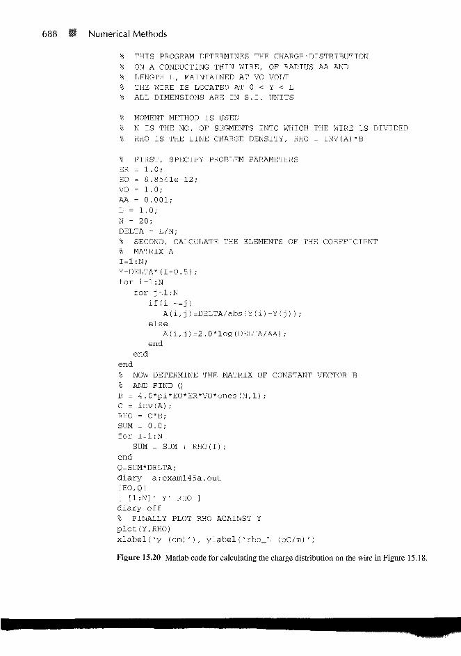
688 Numerical Methods
% THIS PROGRAM DETERMINES THE CHARGE'DISTRIBUTION% ON A CONDUCTING THIN WIRE, OF RADIUS AA AND% LENGTH L, MAINTAINED AT VO VOLT% THE WIRE IS LOCATED AT 0 < Y < L% ALL DIMENSIONS ARE IN S.I. UNITS
% MOMENT METHOD IS USED% N IS THE NO. OF SEGMENTS INTO WHICH THE WIRE IS DIVIDED% RHO IS THE LINE CHARGE DENSITY, RHO = INV(A)*B
% FIRST, SPECIFY PROBLEM PARAMETERSER = 1.0;EO = 8.8541e-12;VO = 1.0;AA = 0.001;L = 1.0;N = 20;DELTA = L/N;% SECOND, CALCULATE THE ELEMENTS OF THE COEFFICIENT% MATRIX A
Y=DELTA*(I-O.5);for i=l:N
for j=l:N
if(i ~=j)A(i, j)=DELTA/abs(Y(i)-Y(j) ) ;
elseA(i,j)=2.0*log(DELTA/AA);
endend
end% NOW DETERMINE THE MATRIX OF CONSTANT VECTOR B% AND FIND QB = 4.0*pi*EO*ER*VO*ones(N,1);C = inv(A);RHO = C*B;SUM = 0.0;for I=1:N
SUM = SUM + RHO(I);endQ=SUM*DELTA;diary a:examl45a.out[EO,Q][ [1:N]' Y' RHO ]diary off% FINALLY PLOT RHO AGAINST Yplot(Y,RHO)xlabel{'y (cm)'), ylabel("rho_L (pC/m)')
Figure 15.20 Matlab code for calculating the charge distribution on the wire in Figure 15.18.
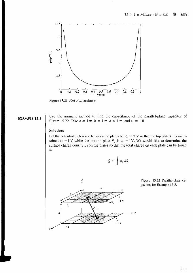
15.4 THE MOMENT METHOD 689
10.5
0 0.1 0.2 0.3 0.4 0.5 0.6 0.7 0.8 0.9 1y(cm)
Figure 15.21 Plot of pL against y.
EXAMPLE 15.5Use the moment method to find the capacitance of the parallel-plane capacitor ofFigure 15.22. Take a = 1 m, b = 1 m, d = 1 m, and sr = 1.0.
Solution:
Let the potential difference between the plates be Vo = 2 V so that the top plate Px is main-tained at +1 V while the bottom plate P2 is at — 1 V. We would like to determine thesurface charge density ps on the plates so that the total charge on each plate can be foundas
Q= PsdS
Figure 15.22 Parallel-plate ca-pacitor; for Example 15.5.
I

690 U Numerical Methods
Once Q is known, we can calculate the capacitance as
C = Q = QV 2
To determine ps using the moment method, we divide P{ into n subsections: AS],AS2,. . ., ASn and P2 into n subsections: A5n+1, ASn+2,. • ., AS2n- The potential V,- at thecenter of a typical subsection AS, is
1ypi 47T£O
PjdS
2nASt
It has been assumed that there is uniform charge distribution on each subsection. The lastequation can be written as
where
Thus
./=!
dS
In
1L7=1
Vn =
In
7=1
In
7 = 1PjAn+\,j = ~

15.4 THE MOMENT METHOD 691
yielding a set of In simultaneous equations with 2n unknown charge densities pj. In matrixform,
An
A21
A12
A22
P\Pi
Pin
11
- 1- 1
or
[A] [p] = [B]
Hence,
[p] [B]
where [B] is the column matrix defining the potentials and [A] is a square matrix contain-ing elements A,-,-. To determine A,-,-, consider the two subsections i and j shown inFigure 15.23 where the subsections could be on different plates or on the same plate.
1 dxdy
where
Ru = [(xj - Xi)2 + (yj- yd2 + (zj
\2-il/2
For the sake of convenience, if we assume that the subsections are squares,
x2 - x\ = A€ = y2 - y\
it can be shown that
AS, (A€)2
Figure 15.23 Subsections i and j ; forExample 15.5.
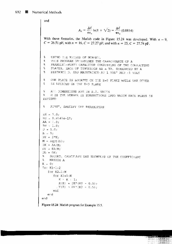
692 11 Numerical Methods
and
An = ln(l + V2) = —(0.8814)7TSO 7TEO
With these formulas, the Matlab code in Figure 15.24 was developed. With n = 9,C = 26.51 pF, with n = 16, C = 27.27 pF, and with n = 25, C = 27.74 pF.
% USING THE METHOD OF MOMENT,% THIS PROGRAM DETERMINES THE CAPACITANCE OF A% PARALLEL-PLATE CAPACITOR CONSISTING OF TWO CONDUCTING% PLATES, EACH OF DIMENSION AA x BB, SEPARATED BY A% DISTANCE D, AND MAINTAINED AT 1 VOLT AND -1 VOLT
% ONE PLATE IS LOCATED ON THE Z = 0 PLANE WHILE THE OTHER% IS LOCATED ON THE Z=D PLANE
% ALL DIMENSIONS ARE IN S.I. UNITS% N IS THE NUMBER IS SUBSECTIONS INTO WHICH EACH PLATE ISDIVIDED
% FIRST, SPECIFY THE PARAMETERS
ER = 1.0;EO = 8.8541e-12;AA = 1.0;BB = 1.0;D = 1.0;N = 9;NT = 2*N;M = sqrt(N);DX = AA/M;DY = BB/M;DL = DX;% SECOND, CALCULATE THE ELEMENTS OF THE COEFFICIENT% MATRIX AK = 0;for Kl=l:2
for K2=1:Mfor K3=1:M
K = K + 1;X(K) = DX*(K2 - 0.5);Y(K) = DY*(K3 - 0.5);
endend
end
Figure 15.24 Matlab program for Example 15.5.
15.4 THE MOMENT METHOD • 693
for Kl=l:NZ(K1) = 0.0;Z(K1+N) = D;
endfor 1=1:NT
for J=1:NTif(I==J)
A(I,J) = DL*0.8814/(pi*EO);elseR = sqrt( (X(I)-X(J))A2 = (Y(I)-Y(J) )A2 + ( Z (I)-Z (J) ) A2 ) ;
A(I,J) = DLA2/(4.*pi*EO*R);end
endend% NOW DETERMINE THE MATRIX OF CONSTANT VECTOR Bfor K=1:N
B(K) = 1.0;B(K+N) = -1.0;
end% INVERT A AND CALCULATE RHO CONSISTING% THE UNKNOWN ELEMENTS% ALSO CALCULATE THE TOTAL CHARGE Q AND CAPACITANCE CF = inv(A);RHO = F*B';SUM = 0.0;for I=1:N
SUM = SUM + RHO(I);endQ = SUM*(DLA2) ;VO = 2.0;C = abs(Q)/VO;diary a:examl45b.out[C][ [1:NT]' X Y' Z' RHO ]diary off
Figure 15.24 (Continued)
PRACTICE EXERCISE 15.5
Using the moment method, write a program to determine the capacitance of two iden-tical parallel conducting wires separated at a distance _yo and displaced by xo as shownin Figure 15.25. If each wire is of length L and radius a, find the capacitance tor casesxo = 0,0.2,0.4,. . ., 1.0m.Take;yo = 0.5 m,L = 1 m,a = 1 mm,er = 1.
Answer: For N = 10 = number of segments per wire, see Table 15.2.
L

694 Numerical Methods
Figure 15.25 Parallel conducting wires of Practice Ex-ercise 15.5.
x = L
TABLE 15.2for Practice
x0 (m)
0.00.20.40.60.81.0
CapacitanceExercise 15.5
C(pF)
4.914.8914.8534.7894.714.643
15.5 THE FINITE ELEMENT METHOD
The finite element method (FEM) has its origin in the field of structural analysis. Themethod was not applied to EM problems until 1968.3 Like the finite difference method, thefinite element method is useful in solving differential equations. As noticed in Section15.3, the finite difference method represents the solution region by an array of grid points;its application becomes difficult with problems having irregularly shaped boundaries. Suchproblems can be handled more easily using the finite element method.
The finite element analysis of any problem involves basically four steps: (a) discretiz-ing the solution region into a finite number of subregions or elements, (b) deriving govern-ing equations for a typical element, (c) assembling of all elements in the solution region,and (d) solving the system of equations obtained.
A. Finite Element Discretization
We divide the solution region into a number of finite elements as illustrated in Figure 15.26where the region is subdivided into four nonoverlapping elements (two triangular and twoquadrilateral) and seven nodes. We seek an approximation for the potential Ve within an
3See P. P. Silvester and R. L. Ferrari, Finite Elements for Electrical Engineers. Cambridge, England:Cambridge Univ. Press, 1983.

15.5 THE FINITE ELEMENT METHOD 695
Figure 15.26 A typical finite element subdi-vision of an irregular domain.
/ node no.
/ ') element no.
7
Actual boundary
Approximate boundary
element e and then interrelate the potential distributions in various elements such that thepotential is continuous across interelement boundaries. The approximate solution for thewhole region is
V(x, y) = X ve(x, y) (15.45)
where N is the number of triangular elements into which the solution region is divided.The most common form of approximation for Ve within an element is polynomial ap-
proximation, namely
for a triangular element and
Ve(x, y) = a + bx + cy
Ve(x> y) = a + bx + cy + dxy
(15.46)
(15.47)
for a quadrilateral element. The potential Ve in general is nonzero within element e but zerooutside e. It is difficult to approximate the boundary of the solution region with quadrilat-eral elements; such elements are useful for problems whose boundaries are sufficientlyregular. In view of this, we prefer to use triangular elements throughout our analysis in thissection. Notice that our assumption of linear variation of potential within the triangularelement as in eq. (15.46) is the same as assuming that the electric field is uniform withinthe element; that is,
Ee = ~VVe = -{bax + cay) (15.48)
B. Element Governing Equations
Consider a typical triangular element shown in Figure 15.27. The potential VeU Ve2, andVe3 at nodes 1, 2, and 3, respectively, are obtained using eq. (15.46); that is,
1 xx yx
1 x 2 y 2
1 X% VQ
(15.49)
696 Numerical Methods
The coefficients a, b, and c are determined from eq. (14.49) as
111
Xl
x2
x3
yi~
y2
yi
~vei~
ve2_ve3_
(15.50)
Substituting this into eq. (15.46) gives
Ve = [1 x v]2A
(x2y3
(y2
(x3
~ x3y2)
-y3)- x 2 )
(X3J, - Xxy3)
(y3 - y\)(Xi — X3)
W 2 — Xj>
-y2)- Xi)
or
(15.51)
where
1
1012 ~U
1a 3 " 2 A
and A is the area of the element e\ that is,
(y2 - (15.52a)
(15.52b)
(15.52c)
2A =1 x3
= (x\y2 - - xxy3) - x3y2)
or
A = 1/2 [x2 - xY)(y3 - yi) - (x3 - X])(y2 - (15.53)
The value of A is positive if the nodes are numbered counterclockwise (starting from anynode) as shown by the arrow in Figure 15.27. Note that eq. (15.51) gives the potential atany point (x, y) within the element provided that the potentials at the vertices are known.This is unlike the situation in finite difference analysis where the potential is known at thegrid points only. Also note that a, are linear interpolation functions. They are called theelement shape functions and they have the following properties:
(15.54a)

15.5 THE FINITE ELEMENT METHOD 697
Figure 15.27 Typical triangular element; the localnode numbering 1-2-3 must be counterclockwise asindicated by the arrow.
2>.<*.)0 = i (15-54b)
The shape functions a^ and a-i, for example, are illustrated in Figure 15.28.The energy per unit length associated with the element e is given by eq. (4.96); that is
(15.55)= ! | e\VVe\2dS
where a two-dimensional solution region free of charge (ps = 0) is assumed. But fromeq. (15.51),
(15.56)
Substituting eq. (15.56) into eq. (15.55) gives
1 i=i j=\
If we define the term in brackets as
f =
Vej
Cf = I Va,- • Vaj dS
(15.57)
(15.58)
3 Figure 15.28 Shape functions a, anda2 for a triangular element.

698 U Numerical Methods
we may write eq. (15.57) in matrix form as
We — — e [Ve]T [C ( e )] [Ve]
where the superscript T denotes the transpose of the matrix,
Ve2
ve3
(15.59)
(15.60a)
and
'(eh _[Ce>] =
Me)e)
C 2
C )33
(15.60b)
The matrix [C(e) is usually called the element coefficient matrix. The matrix element C(f ofthe coefficient matrix may be regarded as the coupling between nodes / andy; its value isobtained from eqs. (15.52) and (15.58). For example,
n = Va? dS
Similarly:
Also
= 77i Kyi - yAA
= — [(y2 ~
el = 7^ Ky2 - yx
i
44
44
1
1 ~ L
+ (x3 - ^2)(x, - x3)] I dS (15.61a)
-x3)]
(15.61b)
(15.61c)
(15.61d)
(15.61e)
(15.61f)
C 3Me) _ WeiL32 — L23 (15.61g)
15.5 THE FINITE ELEMENT METHOD 699
However, our calculations will be easier if we define
Pi = (yi- y3), Pi = (y3 ~ ?i). ^ = Cv. - yd
Qi = (x3 - x2), Q2 = (xi ~ x3), Q3 = (x2 - xi)
(15.62a)
With Pt and Qt (i = 1, 2, 3 are the local node numbers), each term in the element coeffi-cient matrix is found as
(15.62b)
where
A = -(P2Q3 ~ P3Q2) (15.62c)
Note that Px + P2 + /^ = 0 = Ql + Q2 + Q3 and hence
may be used in checking our calculations.
= 0 = 2 ct• This
7 = 1
C. Assembling of All Elements
Having considered a typical element, the next step is to assemble all such elements in thesolution region. The energy associated with the assemblage of all elements in the mesh is
e = l= -s[V]T[C][V] (15.63)
where
[VI =
v,v2
(15.64)
n is the number of nodes, N is the number of elements, and [C\ is called the overall orglobal coefficient matrix, which is the assemblage of individual element coefficient matri-ces. The major problem now is obtaining [C] from [Cw].
The process by which individual element coefficient matrices are assembled to obtainthe global coefficient matrix is best illustrated with an example. Consider the finite elementmesh consisting of three finite elements as shown in Figure 15.29. Observe the numberingsof the nodes. The numbering of nodes as 1, 2, 3, 4, and 5 is called global numbering. Thenumbering i-j-k is called local numbering and it corresponds with 1 -2-3 of the element in
L

700 Numerical Methods
Figure 15.29 Assembly of three elements: i-j-k cor-responds to local numbering 1 -2-3 of the element inFigure 15.27.
Figure 15.27. For example, for element 3 in Figure 15.29, the global numbering 3-5-4 cor-responds with local numbering 1-2-3 of the element in Figure 15.27. Note that the localnumbering must be in counterclockwise sequence starting from any node of the element.For element 3, for example, we could choose 4-3-5 or 5-4-3 instead of 3-5-4 to correspondwith 1-2-3 of the element in Figure 15.27. Thus the numbering in Figure 15.29 is notunique. However, we obtain the same [C] whichever numbering is used. Assuming the par-ticular numbering in Figure 15.29, the global coefficient matrix is expected to have theform
C\\
c2lc3ic4i
c5.
C]2
C22
C32
C42
c52
C,3
C23
C33
c43c53
C34 C-34
C44 C<
' 25
35
45
55
(15.65)
which is a 5 X 5 matrix since five nodes (n = 5) are involved. Again, Cy is the couplingbetween nodes / and j . We obtain Cy by utilizing the fact that the potential distribution mustbe continuous across interelement boundaries. The contribution to the i,j position in [C]comes from all elements containing nodes ;' a n d / To find C u , for example, we observefrom Figure 15.29 that global node 1 belongs to elements 1 and 2 and it is local node 1 inboth; hence,
Cn = Cft + Cft (15.66a)
For C22, global node 2 belongs to element 1 only and is the same as local node 3; hence,
C22 = C ^ (15.66b)
For C44, global node 4 is the same as local nodes 2, 3, and 3 in elements 1, 2, and 3, re-spectively; hence,
_ /-•a)C44 = C m- 3 3
(15.66c)
For C14, global link 14 is the same as the local links 12 and 13 in elements 1 and 2, respec-tively; hence,
4.T
<2)
Since there is no coupling (or direct link) between nodes 2 and 3,
c2 3 = c3 2 = 0
(15.66d)
(15.66e)
15.5 THE FINITE ELEMENT METHOD 701
Continuing in this manner, we obtain all the terms in the global coefficient matrix by in-spection of Figure 15.29 as
(2)31
0
0 C22 -r L-n
0
CXi + C
£(2) +~C(3)
r-0)
00
(15.67)
Note that element coefficient matrices overlap at nodes shared by elements and that thereare 27 terms (nine for each of the three elements) in the global coefficient matrix [C]. Alsonote the following properties of the matrix [C]:
1. It is symmetric (Cy = C,,) just as the element coefficient matrix.2. Since Cy = 0 if no coupling exists between nodes ;' and j , it is evident that for a
large number of elements [C] becomes sparse and banded.3. It is singular. Although this is not so obvious, it can be shown using the element co-
efficient matrix of eq. (15.60b).
D. Solving the Resulting EquationsFrom variational calculus, it is known that Laplace's (or Poisson's) equation is satisfiedwhen the total energy in the solution region is minimum. Thus we require that the partialderivatives of W with respect to each nodal value of the potential be zero; that is,
dW dW dW
dV2= 0
or
dW= 0, k = 1,2,. . .,n (15.68)
For example, to get d Wd V! = 0 for the finite element mesh of Figure 15.29, we substituteeq. (15.65) into eq. (15.63) and take the partial derivative of W with respect to V\. Weobtain
dW0 = — = 2VlCu + V2CU + V3Cl3 + V4Cl4 + V5Cl5
+ v2c2l + v3c31 + v4c4l + v5c51
or
0 = ViCn + V2Cl2 v4ci4 + v5c,5 (15.69)
L

702 Numerical Methods
In general, 3W/dVk = 0 leads to
0 = V, Cik (15.70)
where n is the number of nodes in the mesh. By writing eq. (15.70) for all nodesk = 1,2,. . ., n, we obtain a set of simultaneous equations from which the solution of[V\T = [Vu V2, • . ., Vn] can be found. This can be done in two ways similar to those usedin solving finite difference equations obtained from Laplace's (or Poisson's) equation.
Iteration Method:
This approach is similar to that used in finite difference method. Let us assume that node 1in Figure 15.29, for example, is a free node. The potential at node 1 can be obtained fromeq. (15.69) as
v = -— y vcL-ll i=2
In general, the potential at a free node k is obtained from eq. (15.70) as
(15.71)
(15.72)
This is applied iteratively to all the free nodes in the mesh with n nodes. Since Cki = 0 ifnode k is not directly connected to node /, only nodes that are directly linked to node k con-tribute to Vk in eq. (15.72).
Thus if the potentials at nodes connected to node k are known, we can determine Vk
using eq. (15.72). The iteration process begins by setting the potentials at the free nodesequal to zero or to the average potential.
Vave = 1/2 (Vn- x ) (15.73)
where Vmin and Vmax are the minimum and maximum values of the prescribed potentials atthe fixed nodes. With those initial values, the potentials at the free nodes are calculatedusing eq. (15.72). At the end of the first iteration, when the new values have been calcu-lated for all the free nodes, the values become the old values for the second iteration. Theprocedure is repeated until the change between subsequent iterations becomes negligible.
Band Matrix Method:
If all free nodes are numbered first and the fixed nodes last, eq. (15.63) can be writtensuch that
W= -e\Vf VI Cff Cfpfp\ \Vf (15.74)

15.5 THE FINITE ELEMENT METHOD 703
where subscripts/and p, respectively, refer to nodes with free and fixed (or prescribed) po-tentials. Since Vp is constant (it consists of known, fixed values), we only differentiate withrespect to V -so that applying eq. (15.68) to eq. (15.74) yields
cf = o
or
This equation can be written as
[Cff] [VA = -[Cfc] [Vp]
[A] [V] = [B]
(15.75)
(15.76a)
or
[V] = ~][B] (15.76b)
where [V] = [Vf], [A] = [Cff], and [B] = - [ C y [Vp]. Since [A] is, in general, non-singular, the potential at the free nodes can be found using eq. (15.75). We can solvefor [V\ in eq. (15.76a) using Gaussian elimination technique. We can also solve for [V]in eq. (15.76b) using matrix inversion if the size of the matrix to be inverted is notlarge.
Notice that as from eq. (15.55) onward, our solution has been restricted to a two-dimensional problem involving Laplace's equation, V2V = 0. The basic concepts devel-oped in this section can be extended to finite element analysis of problems involvingPoisson's equation (V2V = —pv/e, V2A = -fij) or wave equation (V2<£ - y2<j> = 0). Amajor problem associated with finite element analysis is the relatively large amount ofcomputer memory required in storing the matrix elements and the associated computa-tional time. However, several algorithms have been developed to alleviate the problem tosome degree.
The finite element method (FEM) has a number of advantages over the finite differ-ence method (FDM) and the method of moments (MOM). First, the FEM can easily handlecomplex solution region. Second, the generality of FEM makes it possible to construct ageneral-purpose program for solving a wide range of problems. A single program can beused to solve different problems (described by the same partial differential equations) withdifferent solution regions and different boundary conditions; only the input data to theproblem need be changed. However, FEM has its own drawbacks. It is harder to under-stand and program than FDM and MOM. It also requires preparing input data, a processthat could be tedious.
EXAMPLE 15.6 Consider the two-element mesh shown in Figure 15.30(a). Using the finite elementmethod, determine the potentials within the mesh.

704 Numerical Methods
Node:1
2
\ 3V=\0 4
(x,y)(0.8, 1.8)(1.4, 1.4)(2.1,2.1)(1.2, 2.7)
Figure 15.30 For Example 15.6: (a) two-elementmesh, (b) local and global numbering of the ele-ments.
- K=0
(a)
(b)
Solution:
The element coefficient matrices can be calculated using eq. (15.62). For element 1,consisting of nodes 1-2-4 corresponding to the local numbering 1-2-3 as in Figure15.30(b),
P, = -1 .3 , P2 = 0.9, P3 = 0.4
Q, = -0.2, Q2 = -0.4, Q3 = 0.6
A = 1/2(0.54 + 0.16) = 0.35
Substituting all these into eq. (15.62b) gives
1.236 -0.7786 -0.4571-0.7786 0.6929 0.0857-0.4571 0.0857 0.3714
(15.6.1)
Similarly, for element 2 consisting of nodes 2-3-4 corresponding to local numbering 1 -2-3as in Figure 15.30(b),
P, = -0.6, P2 = 1.3, P3 = -0.7
G, = "0.9, Q2 = 0.2, & = 0.7
A = 1/2(0.91 + 0.14) = 0.525

15.5 THE FINITE ELEMENT METHOD 705
Hence,
0.5571 -0.4571 -0.1-0.4571 0.8238 -0.3667-0.1 -0.3667 0.4667
Applying eq. (15.75) gives
v2c42 c4 4j [v4
C21 C23
C41 C43
This can be written in a more convenient form as
1000
0C22
0C42
0010
0
c2 40C44
v2
v4
1-C21
0-C41
0- C 2 3
1— C43
or
[Q[V] = [B]
The terms of the global coefficient matrix are obtained as follows:
C22 = C(22} + Cff = 0.6929 + 0.5571 = 1.25
C42 = C24 = C$ + Cfl = 0.0857 - 0.1 = -0.0143
C44 = + C3f = 0.3714 + 0.4667 = 0.8381
C2i = C2\} = -0.7786
(15.6.2.)
(15.6.3)
(15.6.4a)
(15.6.4b)
C23 = C(\2 = -0.4571
C4, = C3V = -0.4571
Q3 = C3f = -0.3667
Note that we follow local numbering for the element coefficient matrix and global num-bering for the global coefficient matrix. Thus the square matrix [C] is obtained as
1 0 0 00 1.25 0 -0.01430 0 1 00 -0.0143 0 0.8381
(15.6.5)

706 Numerical Methods
and the matrix [B] on the right-hand side of eq. (15.6.4a) is obtained as
04.571
10.03.667
(15.6.6)
By inverting matrix [C] in eq. (15.6.5), we obtain
[V\
03.708
10.04.438
Thus V, = 0, V2 = 3.708, V3 = 10, and V4 = 4.438. Once the values of the potentials atthe nodes are known, the potential at any point within the mesh can be determined usingeq. (15.51).
PRACTICE EXERCISE 15.6
Calculate the global coefficient matrix for the two-element mesh shown inFigure 15.31 when: (a) node 1 is linked with node 3 and the local numbering(/ - j - k) is as indicated in Figure 15.31(a), (b) node 2 is linked with node 4 withlocal numbering as in Figure 15.31(b).
Answer: (a)
(b)
0.99640.050.24640.8
1.3330.07770.01.056
0.050.7
-0.750.0
-0.77770.8192
-0.980.2386
-0.2464-0.751.5964
-0.6
0.0-0.982.04
-1.06
-0.80.0
-0.6i.4
-1.0560.2386
-1.061.877
N o d e l : ( 2 , 1 ) N o d e 3 : ( 2 , 2 . 4 )
N o d e 2: ( 3 , 2.5) N o d e 4 : ( 1 .5 , 1.6)
Figure 15.31 For Practice Exercise 15.6.
15.5 THE FINITE ELEMENT METHOD 707
EXAMPLE 15.7Write a program to solve Laplace's equation using the finite element method. Apply theprogram to the two-dimensional problem shown in Figure 15.32(a).
Solution:
The solution region is divided into 25 three-node triangular elements with the totalnumber of nodes being 21 as shown in Figure 15.32(b). This is a necessary step in orderto have input data defining the geometry of the problem. Based on our discussions inSection 15.5, a general Matlab program for solving problems involving Laplace's equa-tion using three-node triangular elements was developed as in Figure 15.33. The devel-
1.0
Figure 15.32 For Example 15.7:(a) two-dimensional electrostaticproblem, (b) solution region di-vided into 25 triangular elements.
100 V
1.0
(a)

708 Numerical Methods
FINITE ELEMENT SOLUTION OF LAPLACE'S EQUATION FORTWO-DIMENSIONAL PROBLEMSTRIANGULAR ELEMENTS ARE USEDND = NO. OF NODESNE = NO. OF ELEMENTSNP = NO. OF FIXED NODES ' (WHERE POTENTIAL IS PRESCRIBED)NDP(I) = NODE NO. OF PRESCRIBED POTENTIAL, I=1,2,...,NPVAL(I) = VALUE OF PRESCRIBED POTENTIAL AT NODE NDP(I)NL(I,J) = LIST OF NODES FOR EACH ELEMENT I, WHERE
J=l,2,3 REFERS TO THE LOCAL NODE NUMBERCE(I,J) = ELEMENT COEFFICIENT MATRIXC(I,J) = GLOBAL COEFFICIENT MATRIXB(I) = RIGHT-HAND SIDE MATRIX IN THE SYSTEM OFSIMULTANEOUS EQUATIONS; SEE EQ. (15.6.4)X(I), Y(I) = GLOBAL COORDINATES OF NODE IXL(J), YL(J) = LOCAL COORDINATES OF NODE J=l,2,3V(I) = POTENTIAL AT NODE IMATRICES P(I) AND Q (I) ARE DEFINED IN EQ. (15.62a)
FIRST STEP - INPUT DATA DEFINING GEOMETRY ANDBOUNDARY CONDITIONS
****************************************************
clearinput ("Name of input data file =
% SECOND STEP - EVALUATE COEFFICIENT MATRIX FOR EACHELEMENT AND ASSEMBLE GLOBALLY
^ ****************************************************
B = zeros(ND,1);C = zeros(ND,ND);for 1=1:NE% FIND LOCAL COORDINATES XL(J), YL(J) FOR ELEMENT I
K = NL(I, [1: 3] ) ;XL = X(K);YL = Y(K);
P=zeros(3Q=zeros(3
P(l) =P(2) =P(3) =
Q(D =Q(2) =Q(3) =AREA =
,1) ;,1) ;YL(2) -YL(3) -YL(1) -XL(3) -XL (1) -XL(2) -0.5*abs
YL(3)YL(1)YL(2)XL (2)XL (3)XL(1)( P(2)*Q(3) - Q(2)*P(3) )
Figure 15.33 Computer program for Example 15.7.

15.5 THE FINITE ELEMENT METHOD 709
% DETERMINE COEFFICIENT MATRIX FOR ELEMENT ICE=(P*P'+Q*Q')/(4.0*AREA);
% ASSEMBLE GLOBALLY - FIND C(I,J) AND B(I)for J=l:3
IR = NL(I,J);IFLAG1=O;
% CHECK IF ROW CORRESPONDS TO A FIXED NODEfor K = 1:NP
if (IR == NDP(K))C(IR,IR) = 1.0;B(IR) = VAL(K);IFLAG1=1;
endend % end for K = 1:NPif(IFLAGl == 0)for L = 1:3IC = NL(I,L);IFLAG2=0;
% CHECK IF COLUMN CORRESPONDS TO A FIXED NODEfor K=1:NP
if ( IC == NDP(K) ),B(IR) = B(IR) - CE(J,L)*VAL(K);IFLAG2=1;
endend % end for K=1:NP
if(IFLAG2 == 0)C(IR,IC) = C(IR,IC) + CE(J,L);end
end % end for L=l:3end %end if(ifiagl == 0)
end % end for J=l:3end % end for 1=1:NE
% THIRD STEP - SOLVE THE SYSTEM OF EQUATIONS
V = inv(C)*B;V=V' ;
% FOURTH STEP - OUTPUT THE RESULTS•6
diary examl47.out[ND, NE, NP][ [1:ND]' X' Y' V ]diary off
Figure 15.33 (Continued)
I

710 Numerical Methods
opment of the program basically involves four steps indicated in the program and ex-plained as follows.
Step 1: This involves inputting the necessary data defining the problem. This is the only stepthat depends on the geometry of the problem at hand. Through a data file, we input thenumber of elements, the number of nodes, the number of fixed nodes, the prescribed valuesof the potentials at the free nodes, the x and y coordinates of all nodes, and a list identifyingthe nodes belonging to each element in the order of the local numbering 1-2-3. For theproblem in Figure 15.32, the three sets of data for coordinates, element-node relationship,and prescribed potentials at fixed nodes are shown in Tables 15.3, 15.4, and 15.5, respec-tively.
TABLEof the
15.3Finite
of Figure 15
Node
1
2
3
4
5
6
7
8
9
10
11
X
0.0
0.2
0.4
0.6
0.8
1,0
0,0
0.2
0.4
0.6
0.8
Nodal CoordinatesElement Mesh.32
Y
0.0
0.0
0.0
0.0
0.00.0
0.2
0.2
0.2
0.2
0.2
Node
12
13
14
15
16
17
18
19
20
21
X
0.0
0.2
0.4
0.6
0.0
0.2
0.4
0.0
0.2
0.0
y
0.4
0.4
0.4
0.4
0.6
0.6
0.6
0.8
0.8
1.0
TABLE 15.4 Element-Node Identification
Local Node No. Local Node No.
Element No.
123456789
10111213
1
1223344557889
2
28394
105
11
68
139
14
3
778899
101011
12121313
Element No.
141516171819202122232425
1
91010121313141416171719
2
101511131714181517
201820
3
141415161617171819192021

15.5 THE FINITE ELEMENT METHOD 711
TABLE 15.5 Prescribed
at Fixed Nodes
Node No.
12
3
4
56
11
15
PrescribedPotential
0.0
0.0
0.0
0.0
0.050.0
100.0100.0
Potentials
Node No.
18
20
21
1916127
PrescribedPotential
100.0100.0
50.0
0.00.00.00.0
TABLE 15.6 Input Data for the Finite ElementProgram in Figure 15.33
NENDNPNL
= 25= 21= 15= [2 82 3
8
X =
Y =
NDP
VAL
•;1783344557
2
94
7
89
10 95 1011 1068
138991010121313141416171719
=
9
1 1121213
14 1310 14
000
000
151 1131714181517201820
. 0
. 2
.6
.0
. 2• 4
; i
; o55
141516161717181919202 1 ]
0 .0 .0 .
0 .0 .0 .
2
. 00 . 00 . 0
240
026
3
0 .0 .0 .
0 .0 .0 .
4 5
0 . 01000 . 0
462
026
6
0. 0
0 .0 .0 .
0 .0 .0 .
1 1
. 0
684
026
15
0 .100 .
0 . 0
000
000
00
. 8
. 0
. 0
. 0
. 4
.8
18
0
0 .
100
000
20
. 01000
. 0
. 2
. 2
. 0
. 4
. 8
2 1
. 00 .
0 .0 .0 .
0 .0 .1 .
IS
.0 . . .
.4 . . .
. 0] ;
,2 . . .,4 . . ..0] ;
) 16 12 7 ] ;
100 .00 ] ;
712 Numerical Methods
Step 2: This step entails finding the element coefficient matrix [C^] for each element andthe global coefficient matrix [C]. The procedure explained in the previous example isapplied. Equation (15.6.4) can be written in general form as
1 00 C,•ff.
[Vp]
or
[C] [V] = [B]
Both "global" matrix [C] and matrix [B] are calculated at this stage.
Step 3: The global matrix obtained in the previous step is inverted. The values of the po-tentials at all nodes are obtained by matrix multiplication as in eq. (15.76b). Instead of in-verting the global matrix, it is also possible to solve for the potentials at the nodes usingGaussian elimination technique.
Step 4: This involves outputting the result of the computation.The input and output data are presented in Tables 15.6 and 15.7, respectively.
TABLE:i5.7the Program
Node
1234
5
6
7
8
9
10
11
12
13
14
15
16
17
18192021
X
0.00
0.20
0.40
0.60
0.80
1.00
0.00
0.20
0.40
0.60
0.80
0.00
0.20
0.40
0.60
0.00
0.20
0.40
0.00
0.20
0.00
Output 1Data ofin Figure 15.33
Y
0.00
0.00
0.00
0.00
0.00
0.00
0.20
0.20
0.20
0.20
0.20
0.40
0.40
0.40
0.40
0.60
0.60
0.60
0.80
0.80
1.00
Potential
0.000
0.000
0.000
0.000
0.000
50.000
0.000
18.182
36.364
59.091
100.000
0.000
36.364
68.182
100.000
0.000
59.091
100.000
0.000
100.000
50.000

y= 2.5
SUMMARY ** 713
22 23 24 25 26 Figure 15.34 For Practice Exercise 15.7.
PRACTICE EXERCISE 15.7
Rework Example 15.3 using the finite element method. Divide the solution regioninto triangular elements as shown in Figure 15.34. Compare the solution with thatobtained in Example 15.3 using the finite difference method.
Answer: See Example 15.3.
SUMMARY 1. Electric field lines and equipotential lines due to coplanar point sources can be plottedusing the numerical technique presented in this chapter. The basic concept can be ex-tended to plotting magnetic field lines.
2. An EM problem in the form of a partial differential equation can be solved using thefinite difference method. The finite difference equation that approximates the differen-tial equation is applied at grid points spaced in an ordered manner over the whole solu-tion region. The field quantity at the free points is determined using a suitable method.
3. An EM problem in the form of an integral equation is conveniently solved using themoment method. The unknown quantity under the integral sign is determined by match-ing both sides of the integral equation at a finite number of points in the domain of thequantity.
4. While the finite difference method is restricted to problems with regularly shaped solu-tion regions, the finite element method can handle problems with complex geometries.This method involves dividing the solution region into finite elements, deriving equa-tions for a typical element, assembling all elements in the region, and solving the re-sulting system of equations.

714 Numerical Methods
Typical examples on how to apply each method to some practical problems have beenshown. Computer programs for solving the problems are provided wherever needed.
15.1 At the point (1, 2, 0) in an electric field due to coplanar point charges, E = 0.3 ax -0.4 ay V/m. A differential displacement of 0.05 m on an equipotential line at that pointwill lead to point
(a) (1.04,2.03,0)
(b) (0.96, 1.97,0)
(c) (1.04,1.97,0)
(d) (0.96, 2.03, 0)
15.2 Which of the following is not a correct finite difference approximation to dV/dx at xo ifh = Ax?
(a)
(b)
(c)
(d)
(e)
V(xo + h) - V{xo)
V(xo)
V(xo-
V(xo-
V(xo-
h
- V(xo
h
f h)-h
f h)-2h
f h/2) -
- h)
V(xo-
V(x0-
- V(xo
h)
h)
- h/2)
15.3 The triangular element of Figure 15.35 is in free space. The approximate value of the po-tential at the center of the triangle is
(a) 10 V
(b) 7.5 V
(c) 5 V(d) 0 V
15.4 For finite difference analysis, a rectangular plate measuring 10 by 20 cm is divided intoeight subregions by lines 5 cm apart parallel to the edges of the plates. How many freenodes are there if the edges are connected to some source?
(a) 15
(b) 12
(c) 9

REVIEW QUESTIONS 715
(2,3) Figure 15.35 For Review Questions 15.3 and 15.10.
-20 V
(3,0)
(d) 6
(e) 3
15.5 Using the difference equation Vn = Vn^l + Vn+1 with Vo = Vs = 1 and starting withinitial values Vn = 0 for 1 < « < 4, the value of V2 after the third iteration is
(a) 1
(b) 3
(c) 9
(d) 15
(e) 25
15.6 The coefficient matrix [A] obtained in the moment method does not have one of theseproperties:
(a) It is dense (i.e., has many nonzero terms).
(b) It is banded.
(c) It is square and symmetric.
(d) It depends on the geometry of the given problem.
15.7 A major difference between the finite difference and the finite element methods is that
(a) Using one, a sparse matrix results in the solution.
(b) In one, the solution is known at all points in the domain.
(c) One applies to solving partial differential equation.
(d) One is limited to time-invariant problems.
15.8 If the plate of Review Question 14.4 is to be discretized for finite element analysis suchthat we have the same number of grid points, how many triangular elements are there?
(a) 32
(b) 16
(c) 12
(d) 9

716 Numerical Methods
PROBLEMS
15.9 Which of these statements is not true about shape functions?
(a) They are interpolatory in nature.
(b) They must be continuous across the elements.
(c) Their sum is identically equal to unity at every point within the element.
(d) The shape function associated with a given node vanishes at any other node.
(e) The shape function associated with a node is zero at that node.
15.10 The area of the element in Figure 15.35 is
(a) 14
(b) 8
(c) 7
(d) 4
Answers: 15.1a, 15.2c,4 15.3a, 15.4e, 15.5c, 15.6b, 15.7a, 15.8b, 15.9e, 15.10d.
15.1 Using the program developed in Example 15.1 or your own equivalent code, plot theelectric field lines and equipotential lines for the following cases:
(a) Three point charges - 1 , 2, and 1 C placed at ( - 1 , 0), (0,2), and (1,0), respec-tively.
(b) Five identical point charges 1 C located at ( - 1, - 1 ) , ( - 1 , 1), (1, - 1 ) , (1, 1), and(0, 0), respectively.
15.2 Given the one-dimensional differential equation
dx2 0 < x <
subject to y(0) = 0, y(l) = 10, use the finite difference (iterative) method to findy(0.25). You may take A = 0.25 and perform 5 iterations.
dV d2V15.3 (a) From the table below, obtain — and ,
dx dx2atx = 0.15.
X
V
0.1
1.0017
0.15
1.5056
0.2
2.0134
0.25
2.5261
0.3
3.0452
(b) The data in the table above are obtained from V = 10 sinh x. Compare your resultin part (a) with the exact values.
4The formula in (a) is known as a forward-difference formula, that in (b) as a backward-differenceformula, and that in (d) or (e) as a central-difference formula.

PROBLEMS 717
m = 0
Figure 15.36 Finite difference grid in cylindri-cal coordinates; for Problem 15.5.
= o
15.4 Show that the finite difference equation for Laplace's equation in cylindrical coordi-nates, V = V(p, z), is
V(p0 , Zo) = \ I V(po, Z
V(po + A,
where h = Az — Ap.
- ^ - ) V( P o - fc, Z o )
15.5 Using the finite difference representation in cylindrical coordinates (p, 4>) at a grid pointP shown in Figure 15.36, let p = m Ap and <j> = n A<f> so that V(p, 4>)\p =V(mAp, nA<t>) = V"m. Show that
1
(w A(t>f(V"~l - 2 V" + V ">
15.6 A square conducting trough has its four sides held at potentials —10, 0, 30, and 60 V.Determine the potential at the center of the trough.
15.7 Use FDM to calculate the potentials at nodes 1 and 2 in the potential system shown inFigure 15.37.
-30 V Figure 15.37 For Problem 15.7.
- 2 0 V
\
/
1
/
2
\
\20 V
0V
I

718 Numerical Methods
100 V
\
Figure 15.38 For Problem 15.9.
\
1
3
2
4
OV
10015.8 Rework Problem 15.7 if ps = nC/m ,h = 0.lm, and e = eo, where h is the mesh
size.
15.9 Consider the potential system shown in Figure 15.38. (a) Set the initial values at the freenodes equal to zero and calculate the potential at the free nodes for five iterations,(b) Solve the problem by the band matrix method and compare result with part (a).
15.10 Apply the band matrix technique to set up a system of simultaneous difference equationsfor each of the problems in Figure 15.39. Obtain matrices [A] and [B].
15.11 (a) How would you modify matrices [A] and [B] of Example 15.3 if the solution regionhad charge density ps?
(b) Write a program to solve for the potentials at the grid points shown in Figure 15.40assuming a charge density ps = x(y — 1) nC/m . Use the iterative finite differencemethod and take er = 1.0.
—
oov-i-
v =
a
d
V =
100 V
b
e
OV
c
f
/
\
1
4
7
2
5
8
/
3 \
6
A • 1 5 V
(a) (b)
Figure 15.39 For Problem 15.10.
-10V
20/
a
d
g
V
b
e
h
c
f
i
/ov
PROBLEMS
Figure 15.40 For Problem 15.11.
719
1.0
15.12 The two-dimensional wave equation is given by
c2 dt2
By letting ^m n denote the finite difference approximation of <P(xm, z,,, tj), show that thefinite difference scheme for the wave equation is
= 2 a (<Pj +
, — 2
<PJ , - 2 <PJ
where /; = Ax = Az and a = (cAt/h)2.
15.13 Write a program that uses the finite difference scheme to solve the one-dimensionalwave equation
d2V d2V
dxz0 < x < 1, > 0
given boundary conditions V(0, i) = 0, V(l, t) = 0, t > 0 and the initial conditiondV/dt (x, 0) = 0, V(x, 0) = sin 7TJC, 0 < JC < 1. Take Ax = At = 0.1. Compare yoursolution with the exact solution V(x, t) = sin 7rx COS TT/ for 0 < t < 4.
15.14 (a) Show that the finite difference representation of Laplace's equation using the nine-
node molecule of Figure 15.41 is
Vo = 1/8 (V, + V2 + V3 + V4 + V5 + V6 + V1 + Vs)
(b) Using this scheme, rework Example 15.4.
15.15 A transmission line consists of two identical wires of radius a, separated by distance d asshown in Figure 15.42. Maintain one wire at 1 V and the other at — 1 V and use MOM tofind the capacitance per unit length. Compare your result with exact formula for C inTable 11.1. Take a = 5 mm, d = cm, € = 5 m, and e = eo.
15.16 Determine the potential and electric field at point (—1,4 , 5) due to the thin conducting
wire of Figure 15.19. Take Vo = 1 V, L = 1 m, a = 1 m m .
L
720 • Numerical Methods
4 3
0
2 Figure 15.41 Nine-node molecule of Problem 15.14.
15.17 Two conducting wires of equal length L and radius a are separated by a small gap and in-clined at an angle 6 as shown in Figure 15.43. Find the capacitance between the wiresusing the method of moments for cases 6 = 10°, 20°,. . ., 180°. Take the gap as 2 mm,a = 1 mm, L = 2 m, er = 1.
15.18 Given an infinitely long thin strip transmission line shown in Figure 15.44(a), we want todetermine the characteristic impedance of the line using the moment method. We divideeach strip into N subareas as in Figure 15.44(b) so that on subarea i,
V,=
where
Ry is the distance between the rth and jth subareas, and V,• = 1 or - 1 depending onwhether the rth subarea is on strip 1 or 2, respectively. Write a program to find the char-acteristic impedance of the line using the fact that
Zn =C
Figure 15.42 For Problem 15.15.

PROBLEMS 721
i For Problem 15.17.
gap2a
where C is the capacitance per unit length and
and Vd = 2 V is the potential difference between strips. Take H = 2 m, W = 5 m, andiV= 20.
15.19 Consider the coaxial line of arbitrary cross section shown in Figure 15.45(a). Using themoment method to find the capacitance C per length involves dividing each conductorinto N strips so that the potential on they'th strip is given by
2N
where
-A€
* « =In
-A€ I. At, , .-z— In—'- - 1.52xe r i=j
J
(a)
I igure 15.44 Analysis of strip transmission line using momentmethod; for Problem 15.18.
722 Numerical Methods
AS,
(b)
Figure 15.45 For Problem 15.19; coaxial line of (a) arbitrary crosssection, and (b) elliptical cylindrical cross section.
and Vj; = - 1 or 1 depending on whether A€,- lies on the inner or outer conductor respec-tively. Write a Matlab program to determine the total charge per length on a coaxial cableof elliptical cylindrical cross section shown in Figure 15.45(b) using
and the capacitance per unit length using C = Q/2.
(a) As a way of checking your program, take A = B = 2 cm and a = b = 1 cm(coaxial line with circular cross section), and compare your result with the exactvalue of C = 2ire/ ln(A/a).
(b) Take A = 2 cm, B = 4 cm, a = 1 cm, and b = 2 cm.(Hint: For the inner ellipse of Figure 15.45(b), for example,
r =V sin2 v2cos2
where v = alb, di = r d<j>. Take ro = 1 cm.)
15.20 The conducting bar of rectangular cross section is shown in Figure 15.46. By dividing thebar into Nequal segments, we obtain the potential at theyth segment as
where
4-ireoRy
. 2eo=j
PROBLEMS 723
Figure 15.46 For Problem 15.20.
and A is the length of the segment. If we maintain the bar at 10 V, we obtain
= 10[7]
where [/] = [ 1 1 1 . . .if and q{ = pvthA.
(a) Write a program to find the charge distribution pv on the bar and take € = 2 m,h = 2 cm, t = 1 cm, and N = 20.
(b) Compute the capacitance of the isolated conductor using
C= Q/V= (<?, + q2+. . . + qN)/10
15.21 Another way of defining the shape functions at an arbitrary point (x, y) in a finiteelement is using the areas AX,A2, and A3 shown in Figure 15.47. Show that
a* = 4*. 4 = 1 , 2 , 3A
where A = A, + A2 + A3 is the total area of the triangular element.
15.22 For each of the triangular elements of Figure 15.48,
(a) Calculate the shape functions.
(b) Determine the coefficient matrix.
15.23 The nodal potential values for the triangular element of Figure 15.49 are VY = 100 V,V2 = 50 V, and V3 = 30 V. (a) Determine where the 80 V equipotential line intersectsthe boundaries of the element, (b) Calculate the potential of (2, 1).
Figure 15.47 For Problem 15.21.
724 Numerical Methods
(0.5,1)
(0,0)
(a)
Figure 15.48 Triangular elementsof Problem 15.22.
(1,2) (2.5,2)
(2, 0.4)
(b)
15.24 The triangular element shown in Figure 15.50 is part of a finite element mesh. IfVx = 8 V, V2 = 12 V, and V3 = 10 V, find the potential at (a) (1,2) and (b) the centerof the element.
15.25 Determine the global coefficient matrix for the two-element region shown in Figure15.51.
15.26 Find the global coefficient matrix of the two-element mesh of Figure 15.52.
15.27 For the two-element mesh of Figure 15.52, let Vx = 10 V and V3 = 30 V. Find V2 andV4.
(j .j . 2
(2,2)
( 3 , 1 )
Figure 15.-W For Problem 15.23.
(0,0)
(1,4) Fimire 15.50 For Problem 15.24.
(2, -1)
PROBLEMS
Fijiure 15.51 For Problem 15.25.
725
(0,0) (8,0)
(0,1)
(2,2)
Figure 15.52 For Problem 15.26 and 15.27.
(3,0)
15.28 The mesh in Figure 15.53 is part of a large mesh. The shading region is conducting andhas no elements. Find C5S and C5>1.
15.29 Use the program in Figure 15.33 to solve Laplace's equation in the problem shown inFigure 15.54 where Vo = 100 V. Compare the finite element solution to the exact solu-tion in Example 6.5; that is,
i// ^ 4 V ° -ST sin WTT x sinh nwyV(x, y) = V ,
7T ^ o n sinh nit
n = 2k + 1
4 cm 7
Fi»nre 15.53 For Problem 15.28.
L

726 • Numerical Methods
3f
25
19
13
32 33 34 3536 -d=r V,
30
24
18
12
5 6x=1.0
Figure 15.54 For Problem 15.29.
15.30 Repeat the preceding problem for Vo = 100 sin irx. Compare the finite element solutionwith the theoretical solution [similar to Example 6.6(a)]; that is,
V(x, y) =100 sin it x sinh ir y
sinh 7T
15.31 Show that when a square mesh is used in FDM, we obtain the same result in FEM whenthe squares are cut into triangles.

Appendix A
MATHEMATICAL FORMULAS
A.1 TRIGONOMETRIC IDENTITIES
tan A =
sec A =
sin A
cos A'
1
cos A'
cot A =1
esc A =
tan A
1
sin A
sin2 A + cos2 A = 1 , 1 + tan2 A = sec2 A
1 + cot2 A = esc2 A
sin (A ± B) = sin A cos B ± cos A sin B
cos (A ± B) = cos A cos B + sin A sin B
2 sin A sin B = cos (A - B) - cos (A + B)
2 sin A cos B = sin (A + B) + sin (A - B)
2 cos A cos B = cos (A + B) + cos (A - B)
sin A + sin B = 2 sinB A -B
cos
. „ „ A + B A - Bsin A - sin B = 2 cos sin
A - BA + Bcos A + cos B = 2 cos cos
A n ^ . A + B A -Bcos A - cos B = - 2 sin sin
cos (A ± 90°) = +sinA
sin (A ± 90°) = ± cos A
tan (A ±90°) = -cot A
cos (A ± 180°) = -cos A
sin (A ± 180°) = -sin A
727

728 Appendix A
tan (A ± 180°) = tan A
sin 2A = 2 sin A cos A
cos 2A = cos2 A - sin2 A = 2 cos2 A - 1 = 1 - 2 sin2 A
tan A ± Btan (A ± B) = ——
tan 2A =
1 + tan A tan B
2 tan A
1 - tan2 A
sin A =ejA - e~iA
cos A =2/ ' — " 2
ejA = cos A + y sin A (Euler's identity)
TT = 3.1416
1 rad = 57.296°
\.2 COMPUX VARIABLES
A complex number may be represented as
z = x + jy = r/l = reje = r (cos 0 + j sin
where x = Re z = r cos 0, y = Im z = r sin 0
7 = l, T = -y,
The complex conjugate of z = z* = x — jy = r / - 0 = re je
= r (cos 0 - j sin 0)
(ej9)" = ejn6 = cos «0 + j sin «0 (de Moivre's theorem)
If Z\ = x, + jyx and z2 = ^2 + i)1!. then z, = z2 only if x1 = JC2 and j ! = y2.
Zi± Z2 = (xi + x2) ± j(yi + y2)
or
nr2/o,

APPENDIX A 729
i jy\
or
Z2
Vz = VxTjy = \Trem = Vr /fl/2
2n = (x + /y)" = r" e;nfl = rn /nd (n = integer)
z"» = (X + yj,)"" = r1/n
e ^ " = rVn /din + 27rfc/n (t = 0, 1, 2, , n -
In (re'*) = In r + In e7* = In r + jO + jlkir (k = integer)
A3 HYPERBOLIC FUNCTIONS
sinhx =
tanh x =
u ~ -
ex - e'x
2
sinh x
cosh x
1
coshx =
COttlJt =
ex
1
sechx =
tanhx
1
coshx
cosjx = coshx
coshyx = cosx
sinhx
sinyx — j sinhx,
sinhyx = j sinx,
sinh (x ± y) = sinh x cosh y ± cosh x sinh y
cosh (x ± y) = cosh x cosh y ± sinh x sinh y
sinh (x ± jy) = sinh x cos y ± j cosh x sin y
cosh (x ± jy) = cosh x cos y ±j sinh x sin y
sinh 2x sin 2ytanh (x ± jy) = ± /
cosh 2x + cos 2y cosh 2x + cos 2y
cosh2 x - sinh2 x = 1
sech2 x + tanh2 x = 1
sin (x ± yy) = sin x cosh y ± j cos x sinh y
cos (x ± yy) = cos x cosh y + j sin x sinh y
L

730 • Appendix A
A.4 LOGARITHMIC IDENTITIES
If |
log xy = log x + log y
X
log - = log x - log y
log x" = n log x
log10 x = log x (common logarithm)
loge x = In x (natural logarithm)
l , ln ( l + x) = x
A.5 EXPONENTIAL IDENTITIES
ex =
where e == 2.7182
X ~f"
e
[e
In
x2
2 ! 4
V =
1" =
x3
" 3! +
ex+y
X
x4
4!
A.6 APPROXIMATIONS FOR SMALL QUANTITIES
If \x\ <Z 1,
(1 ± x)n == 1 ± ra
^ = 1 + x
In (1 + x) = x
sinxsinx == x or hm = 1
>0 X
COS — 1
tanx — x

APPENDIX A «K 731
A.7 DERIVATIVES
If U = U(x), V = V(x), and a = constant,
dx dx
dx dx dx
d\U
\
Udx dx
V2
~(aUn) = naUn~i
dx
dx U dx
d 1 dU— In U =dx U dx
d v .t/, dU— a = d In a —dx dx
dx dx
dx dx
— sin U = cos U —dx dx
d dU—-cos U = -sin U —dx dx
d , dU—-tan U = sec £/ —dx dx
d dU— sinh U = cosh [/ —dx dx
— cosh t/ = sinh {/ —dx dx
d . dU— tanh[/ = sech2t/ —<ix dx
dx
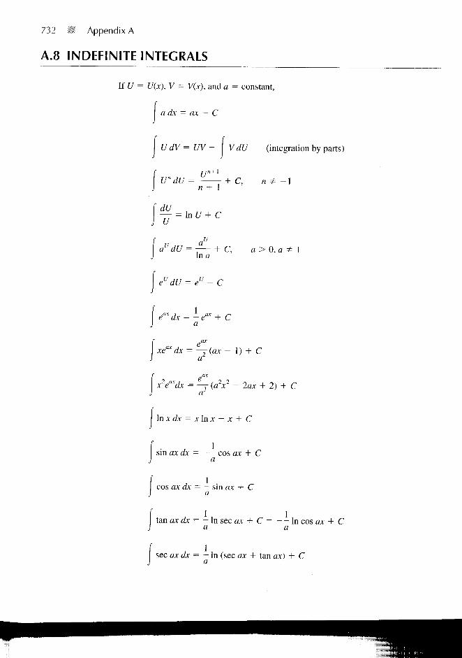
732 Appendix A
A.8 INDEFINITE INTEGRALS
lfU= U(x), V = V(x), and a = constant,
a dx = ax + C
UdV=UV- | VdU (integration by parts)
Un+l
Un dU = + C, n + -1n + 1
dU
U= In U + C
au dU = + C, a > 0, aIn a
eudU = eu +C
eaxdx = - eax + Ca
xeax dx = —r(ax - 1) + C
x eaxdx = — (a2x2 - lax + 2) + C
a'
In x dx = x In x — x + C
sin ax cfcc = — cos ax + Ca
cos ax ax = — sin ax + C
tan ax etc = - In sec ax + C = — In cos ax + Ca a
sec ax ax = — In (sec ax + tan ax) + Ca
APPENDIX A ":: 733
2 x sin 2axsin axdx = — 1- C
2 4a
x sin 2ax2 xcos ax dx = —I
22 4aC
sin ax dx = — (sin ax — ax cos ax) + C
x cos ax dx = —x (cos ax + ax sin ax) + C
eax sin bx dx = —~ r (a sin bx - b cos to) + Ca + ft
eajc cos bx dx = -= ~ (a cos ftx + ft sin /?x) + Ca + b
sin (a - ft)x sin (a + b)x 2 2
sin ax sin ox ax = —— ~ TT,—:—~ •" > a + b
sin ax cos bx dx = —
l(a - b) l(a +
cos (a - b)x cos (a + b)x
cos ax cos bx dx =
a - ft) 2(a + ft)
sin (a - ft)x sin (a + ft)x
2(a - ft) 2(a + b)
C, a1
+ C, a2 # b2
sinh flitfa = - cosh ax + Ca
cosh c a & = - sinh ax + Ca
tanh axdx = -In cosh ax + Ca
ax 1 _• x „- r r = - tan ' - + Cx
2 + a2 a a
X X l ( 2 + 2)2 2
x + a I
C
x2 dx _, x— r = x - a tan - + Cx2 + a ' «

734 Appendix A
dx x + a x2>a2
x2-a2 1 a - x 2 , 2T— In —• h C, x < a2a a + x
dx
\ / 2 ,Vx ±
xdx
x2
2a
_, x= sin ' - + C
= In (x + V x 2 ± a2) + C
a2 + C
dx x/az
(x2 + a2)3'2+ C
xdx
(x2 + a2)3'2 'x2 + a2
x2dx
(x2 + a2f2 = In+ a2 x
a a V + a2 + C
dx
(xz + az
1 / x 1 _! *\r^f "i j + - tan l-} + Cla \x + a a a,
A.9 DEFINITE INTEGRALS
'o
sin mx sin nx dx = cos mx cos nx dx = { ', m + nir/2, m = n
, i w, m + n = evensin mx cos nx dx = I
o i — r, m + n = oddm - «
sin mx sin nx dx = sin mx sin nx dx = J, m =F nw, m = n
sin axir/2, a > 0,
dx = ^ 0, a = 0-ir/2, a < 0
sin2x

APPENDIX A * * 735
f-sin ax , , x
xne~axdx =
'1" dx =
w!
1 Iv
2 V a
a-(ax2+bx+c) £x_ \J_
e M cos bx dx =
e'"1 sin bxdx =a2 + b2
A.10 VECTOR IDENTITIES
If A and B are vector fields while U and V are scalar fields, then
V (U + V) = VU + VV
V (t/V) = U VV + V Vt/
V(VL0 -
V V" = n V " 1 VV (« = integer)
V (A • B) = (A • V) B + (B • V) A + A X (V X B) + B X (V X A)
V • (A X B) = B • (V X A) - A • (V X B)
V • (VA) = V V • A + A • W
V • (VV) = V2V
V • (V X A) = 0
V X ( A + B) = V X A + V X B
V X (A X B) = A (V • B) - B (V • A) + (B • V)A - (A • V)B
V x (VA) = VV X A + V(V X A)
736 Appendix A
V x (VV) = 0
V X (V X A) = V(V • A) - V2A
A • d\ = I V X A - d S
Vd\ = - I VV X dS
A • dS = V • A dv
K
VdS = \ Wdv
A X J S = -

Appendix D
MATERIAL CONSTANTS
TABLE B.1 Approximate Conductivity* of SomeCommon Materials at 20°C
Material
Conductors
Silver
Copper (standard annealed)
Gold
AluminumTungstenZincBrass
Iron (pure)
Lead
Mercury
Carbon
Water (sea)Semiconductors
Germanium (pure)Silicon (pure)
Insulators
Water (distilled)
Earth (dry)BakelitePaperGlassPorcelainMicaParaffin
Rubber (hard)
Quartz (fused)Wax
Conductivity (siemens/meter)
6.1 X 10'5.8 X 10'4.1 X 10'3.5 X 10'1.8 x 10'1.7 x 10'1.1 x 10'
10'5 X 10⁶
106
3 X 10⁴
4
2.24.4 X 10"4
io-4
io-5
io-'°io-"l O " 1 2
io-'2
io-'5
l O " 1 5
io-'5
io-"10""
The values vary from one published source to another due to the factthat there are many varieties of most materials and that conductivityis sensitive to temperature, moisture content, impurities, and the like.
737

738 Appendix B
TABLE B.2 Approximate Dielectric Constantor Relative Permittivity (er) and Strengthof Some Common Materials*
Material
Barium titanate
Water (sea)
Water (distilled)
NylonPaperGlassMicaPorcelain
Bakelite
Quartz (fused)
Rubber (hard)WoodPolystyrenePolypropyleneParaffin
Petroleum oil
Air (1 atm.)
Dielectric Constanter (Dimensionless)
1200
80
81
87
5-106
65
5
3.12.5-8.0
2.552.25
2.22.1
1
Dielectric StrengthRV/m)
7.5 x 10⁶
12 X 10"
35 x 106
70 X 106
20 X 106
30 X 106
25 X 106
30 X 106
12 X 106
3 X 10⁶
*The values given here are only typical; they vary from onepublished source to another due to different varieties of mostmaterials and the dependence of er on temperature, humidity, and thelike.

APPENDIX B 739
TABLE B.3 RelativePermeability (/*,) ofSome Materials*
Material
Diamagnetic
Bismuth
Mercury
Silver
LeadCopper
Water
Hydrogen (s.t.p.)
Paramagnetic
Oxygen (s.t.p.)
Air
Aluminum
Tungsten
Platinum
Manganese
Ferromagnetic
Cobalt
Nickel
Soft iron
Silicon-iron
V-r
0.999833
0.999968
0.9999736
0.9999831
0.99999060.9999912
= 1.0
0.999998
1.00000037
1.000021
1.00008
1.0003
1.001
250
600
5000
7000
*The values given here are only typical;they vary from one published source toanother due to different varieties ofmost materials.

Appendix C
ANSWERS TO ODD-NUMBEREDPROBLEMS
CHAPTER 1
1.11.3
-0.8703aJC-0.3483a,-0.3482a,(a) 5a* + 4a, + 6s,(b) - 5 3 , - 3s, + 23a,(c) 0.439a* - 0.11a,-0.3293az
(d) 1.1667a* - 0.70843, - 0.7084az
1.7 Proof1.9 (a) -2.8577
(b) -0.2857a* + 0.8571a,(c) 65.91°
1.11 72.36°, 59.66°, 143.91°1.13 (a) (B • A)A - (A • A)B
(b) (A • B)(A X A) - (A •1.15 25.721.17 (a) 7.681
(b)(c) 137.43C
(d) 11.022(e) 17.309
1.19 (a) Proof(b) cos 0! cos 02 + sin i
- 0 i
0.4286a,
A)(A X B)
- 2 a , - 5a7
sin 02, cos 0i cos 02 — sin 0, sin 02
(c) sin
1.21 (a) 10.3(b) -2.175ax + 1.631a, 4.893a.(c) -0.175ax + 0.631ay - 1.893a,
740

APPENDIX C 741
CHAPTER 2
2.1 (a) P(0.5, 0.866, 2)(b) g(0, 1, -4 )(c) #(-1.837, -1.061,2.121)(d) 7(3.464,2,0)
2.3 (a) pz cos 0 - p2 sin 0 cos 0 + pz sin 0(b) r2(l + sin2 8 sin2 0 + cos 8)
2.5 (a) -, 2 4 s i n 0 \ /
(pap + 4az), I sin 8 H ] ar + sin 0 ( cos i
+ / V x 2 + y2 + z2.9 Proof
2.11 (a)xl + yz yz\), 3
(b) r(sin2 0 cos 0 + r cos3 0 sin 0) ar + r sin 0 cos 0 (cos 0 — r cos 0 sin 0) a#, 32.13 (a) r sin 0 [sin 0 cos 0 (r sin 0 + cos 0) ar + sin 0 (r cos2 0 - sin 0 cos 0)
ag + 3 cos 0 a^], 5a# - 21.21a0
p - •- z a A 4.472ap + 2.236az
2.15 (a) An infinite line parallel to the z-axis(b) Point ( 2 , - 1 , 10)(c) A circle of radius r sin 9 = 5, i.e., the intersection of a cone and a sphere(d) An infinite line parallel to the z-axis(e) A semiinfinite line parallel to the x-y plane(f) A semicircle of radius 5 in the x-y plane
2.17 (a) a - ay + 7az
(b) 143.26°(c) -8.789
2.19 (a) -ae(b) 0.693lae
(c) - a e + O.6931a0
(d) 0.6931a,,,2.21 (a) 3a0 + 25a,, -15.6a r + lOa0
(b) 2.071ap - 1.354a0 + 0.4141a,(c) ±(0.5365ar - 0.1073a9 + 0.8371a^,)
2.23 (sin 8 cos3 0 + 3 cos 9 sin2 0) ar + (cos 8 cos3 0 + 2 tan 8 cos 6 sin2 0 -sin 6 sin2 0) ae + sin 0 cos 0 (sin 0 - cos 0) a0

742 I f Appendix C
CHAPTER 3
3.1
3.3
3.53.7
3.93.11
3.13
3.153.17
3.19
3.213.233.25
3.273.29
3.31
3.333.35
(a)(b)(c)(a)(b)(c)
2.3560.52364.18961104.538
0.6667(a)(b)
4a,(a)(b)(a)(b)(c)
- 5 0-39.5
, + 1.333az
( -2 , 0, 6.2)-2a* + (2 At +-0.5578ax - 0.2.5ap + 2.5a0 -- a r + 0.866a<,
Along 2a* + 2a>, -(a)(b)
(a)(b)2(z:
-y2ax + 2zay -(p2 - 3z2)a0 +
COt (7 COS (p ~
Proof2xyz
z - y 2 - y )Proof(a)(b)(c)(d)
6yzax + 3xy2ay •
Ayzax + 3xy2a3, •
6xyz + 3xy3 + ;2(x2 + y2 + z2)
Proof(a)(b)
(c)
(a)
(b)
(c)
(6xy2 + 2x2 + x3z(cos 4> + sin 4
e~r sin 6 cos </>( ]
7
67
6Yes
50.265(a)(b)(c)
Proof, both sidesProof, both sidesProof, both sides
5)3;, m/s8367ay - 3.047a,- 17.32az
az
x\, 04p2az, 0
1 / c o s <t>r- , . + COS
r V sin 6
+ 3x2yzaz
•f 4x2yzaz
\x2yz
•5y2)exz, 24.46»), -8 .1961
A \
L - - j , 0.8277
equal 1.667equal 131.57equal 136.23
6 a* 0

APPENDIX C 743
CHAPTER 4
3.37 (a) 4TT - 2(b) 1-K
3.39 03.41 Proof3.43 Proof3.45 a = 1 = 0 = 7, - 1
4.1 -5.746a., - 1.642a, + 4.104a, mN4.3 (a) -3.463 nC
(b) -18.7 nC4.5 (a) 0.5 C
(b) 1.206 nC(c) 157.9 nC
MV/m
4.134.154.17
4.194.21
4.23
(a) Proof(b) 0.4 mC, 31.61a,/iV/m-0.591ax-0.18a zNDerivation(a) 8.84xyax + 8.84x2a, pC/m2
(b) 8.84>>pC/m3
5.357 kJProof
(0, p<\
1 < p < 2
28P
4.25 1050 J4.27 (a) -1250J
(b) -3750 nJ(c) 0J(d) -8750 nJ
4.29 (a) -2xax - Ayay - 8zaz
(b) -(xax + yay + zaz) cos (x2 + y2 + z2)m
(c) -2p(z + 1) sin 4> ap - p(z + 1) cos <j> a0 - p2 sin <t> az
(d) e"r sin 6 cos 20 ar cos 6 cos 20 ae H sin 20
4.31
4.33
(a)(b)
72ax
- 3 0Proof
+.95
27a, -PC
36a, V/m
744 • Appendix C
4.35 (a)
(b)
(c)
CHAPTER 5
2po 2p0
I5eor2 n I5eor
1) Psdr--^5 J &r' eoV20 6
2po 1 poa15eo 60sn
15(d) Proof
4.37 (a) -1.136 a^kV/m(b) (a, + 0.2a^) X 107 m/s
4.39 Proof,
4.41
(2 sin 0 sin 0 ar - cos 0 sin <t> ae - cos 0 a^) V/m
4.43 6.612 nJ
5.1 -6.283 A5.3 5.026 A5.5 (a) - 16ryz eo, (b) -1.131 mA5.7 (a) 3.5 X 10⁷ S/m, aluminum
(b) 5.66 X 10⁶A/m2
5.9 (a) 0.27 mil(b) 50.3 A (copper), 9.7 A (steel)(c) 0.322 mfi
5.11 1.0001825.13 (a) 12.73zaznC/m2, 12.73 nC/m3
(b) 7.427zaz nC/m2, -7.472 nC/m3
5.15 (a)4?rr2
(b) 0
(o e
1
Q4-Kb2
5.17 -24.72a* - 32.95ay + 98.86a, V/m5.19 (a) Proof
( b ) ^
5.21 (a) 0.442a* + 0.442ay + 0.1768aznC/m2
(b) 0.2653a* + 0.5305ay + 0.7958a,5.23 (a) 46.23 A
(b) 45.98 ,uC/m3
5.25 (a) 1 8 . 2 ^(b) 20.58(c) 19.23%
APPENDIX C • 745
5.27 (a) -1.061a, + 1.768a,, + 1.547az nC/m2
(b) -0.7958a* + 1.326a, + 1.161aznC/m2
(c) 39.79°5.29 (a) 387.8ap - 452.4a,*, + 678.6azV/m, 12a, - 14a0 + 21aznC/m2
(b) 4a, - 2a , + 3az nC/m2, 0(c) 12.62 mJ/m3 for region 1 and 9.839 mJ/m3 for region 2
5.31 (a) 705.9 V/m, 0° (glass), 6000 V/m, 0° (air)(b) 1940.5 V/m, 84.6° (glass), 2478.6 V/m, 51.2° (air)
5.33 (a) 381.97 nC/m2
0955a, 2
(b) 5—nC/mr
(c) 12.96 pi
CHAPTER 6
6.1 120a* + 1203,, " 12az' 5 3 0 - 5 2 1, . , , . PvX3 , PoX2 , fV0 pod\ (py PaX Vo pod\
pod s0V0 s0V0 pod( b ) 3 ~ d ' d + 6
6.5 157.08/ - 942.5;y2 + 30.374 kV6.7 Proof6.9 Proof6.11 25z kV, -25az kV/m, -332az nC/m2, ± 332az nC/m2
6.13 9.52 V, 18.205ap V/m, 0.161a,, nC/m2
6.15 11.7 V, -17.86aeV/m6.17 Derivation
6.19
6.216.236.25
(a)-±
HA 4V°( L ) x
{) x
ProofProofProof
00
V
CO
n = odd
Ddd
sin
i
sin
1
m I
niry
a
1 bnira
n sinhb
nirxsinh
a
n-wbn sinh
aniry
b
n
• h n 7 r
( n ,
b
sinh

746 Appendix C
6.276.296.31
6.33
6.35
6.376.396.416.436.456.47
6.49
0.5655 cm2
Proof(a) 100 V(b) 99.5 nC/m2, - 99(a) 25 pF(b) 63.662 nC/m2
4x
1 1 1 1c d be21.85 pF693.1 sProofProof0.7078 mF(a) lnC(b) 5.25 nN-0.1891 (a, + av + .
.5 nC/m2
1 1a b
a7)N6.51 (a) -138 .24a x - 184.32a, V/m
(b) -1.018 nC/m2
CHAPTER 7
7.1 (b) 0.2753ax + 0.382ay H7.3 0.9549azA/m7.5 (a) 28.47 ay mA/m
(b) -13a , + 13a, mA/m(c) -5.1a, + 1.7ay mA/n(d) 5.1ax + 1.7a, mA/m
7.7 (a) -0.6792az A/m(b) 0.1989azmA/m(c) 0.1989ax
7.9 (a) 1.964azA/m(b) 1.78azA/m(c)(d)
7.11 (a)(b)(c)
7.13 (a)
0.1404a7A/m
0.1989a, A/m
-0.1178a, A/m-0.3457a,, - 0.3165ay + 0.1798azA/mProof1.78 A/m, 1.125 A/mProof1.36a7A/m
(b) 0.884azA/m7.15 (a) 69.63 A/m
(b) 36.77 A/m

APPENDIX C 747
7.17 (b)
0,/ (p2-a2
2-KP \b2 - a2
I
p < a
a< p<b
p>b
7.19
7.21
7.23
7.257.27
7.29
7.31
(a) -2a, A/m2
(b) Proof, both sides equal -30 A(a) 8Oa0nWb/m2
(b) 1.756/i Wb(a) 31.433, A/m(b) 12.79ax + 6.3663, A/m13.7 nWb(a) magnetic field(b) magnetic field(c) magnetic field(14a, + 42a0) X 104 A/m, -1.011 WbIoP a
2?ra2 *
7.33 —/
7.35
7.37
7.39
A/m2
28x(a) 50 A(b) -250 AProof
8/Xo/
CHAPTER 8
8.1 -4.4ax + 1.3a, + 11.4a, kV/m8.3 (a) (2, 1.933, -3.156)
(b) 1.177 J8.5 (a) Proof
8.7 -86.4azpN8.9 -15.59 mJ8.11 1.949axmN/m8.13 2.133a* - 0.2667ay Wb/m2
8.15 (a) -18.52azmWb/m2
(b) -4a,mWb/m2
(c) -Il ia, . + 78.6a,,mWb/m2
I

748 Appendix C
8.17
8.19
8.21
8.23
8.258.27
8.29
8.318.338.358.378.398.41
8.43
(a)(b)(c)(d)
5.581.68ax + 204-220az A/m9.5 mJ/m2
476.68 kA/m
2 -a
(a)(b)26.(a)(b)(c)(a)(b)11.
)
25ap + 15a0 -666.5 J/m3, 57.
833^ - 30ay +-5a,, A/m, - 6— 35ay A/m, —
2ay - 326.7az jtWb/m2
- 50az mWb/m2
7 J/m3
33.96a, A/m.283a,, jtWb/m2
110ay^Wb/m2
5ay A/m, 6.283ay /iWb/m2
167.46181 kJ/m3
58 mm5103 turnsProof190.8 A • t, 19,08088.(a)(b)
5 mWb/m2
6.66 mN1.885 mN
Proof
A/m
CHAPTER 9
9.1 0.4738 sin 377?9.3 - 5 4 V9.5 (a) -0.4? V
(b) -2? 2
9.7 9.888 JUV, point A is at higher potential9.9 0.97 mV9.11 6A, counterclockwise9.13 277.8 A/m2, 77.78 A9.15 36 GHz9.17 (a) V • Es = pje, V-H s = 0 , V x E 5
BDX dDy BDZ(b) —— + —— + ^ ~
ox dy ozdBx dBv dBz
dx dy dzd£z dEy _ dBx
dy dz dt
, V X H, = (a -
Pv
= 0

APPENDIX C 749
dEx
dzdEy
dxdHz
dydHx
dzdHy
dx9.19 Proof
dEz
dxdEx _dydHy
dz_dH1_
dxdHx _
dy ~
jJx
Jy
Jz
dB}
dtdBk
dt
I
+
+
BDX
dt
dDy
dtdDz
dt
9.21 - 0 . 3 z 2 s i n l 0 4 r m C / m 3
9.23 0.833 rad/m, 100.5 sin j3x sin (at ay V/m9.25 (a) Yes
(b) Yes(c) No(d) No
9.27 3 cos <j> cos (4 X 10⁶r)a, A/m2, 84.82 cos <j> sin (4 X 10⁶f)az kV/m
( l + 0 ( 3 - p ) , r t 7 .„-,_4TT
9.29 (2 - p)(l + t)e~p~'az Wb/m2, •
9.31 (a) 6.39/242.4°(b) 0.2272/-202.14°(c) 1.387/176.8°(d) 0.0349/-68°
9.33 (a) 5 cos (at - Bx - 36.37°)a3,20
(b) — cos (at - 2z)ap
22.36(c) — j — cos (at - <j) + 63.43°) sin 0 a0
9.35 Proof
CHAPTER 10
10.1 (a) along ax
(b) 1 us, 1.047 m, 1.047 X 10⁶ m/s(c) see Figure C. 1
10.3 (a) 5.4105 +y6.129/m(b) 1.025 m(c) 5.125 X 10⁷m/s(d) 101.41/41.44° 0
(e) -59A6e-J4h44° e ' ^
I
750 Appendix C
—25 I-
Figured For Problem 10.1.
25
-25
25
- 2 5
- 2 5 I-
t= 778
\/2
t= 774
t = Til
10.5
10.7
10.9
10.11
(a) 1.732(b) 1.234(c) (1.091 - jl.89) X 10~nF/in(d) 0.0164 Np/m(a) 5 X 10⁵ m/s(b) 5 m(c) 0.796 m(d) 14.05/45° U(a) 0.05 + j2 /m(b) 3.142 m(c) 108m/s(d) 20 m(a) along -x-direction(b) 7.162 X 10"10F/m(c) 1.074 sin (2 X 10⁸ + 6x)azV/m

APPENDIX C B 751
10.13 (a) lossless(b) 12.83 rad/m, 0.49 m(c) 25.66 rad(d) 4617 11
10.15 Proof10.17 5.76, -0.2546 sin(109r - 8x)ay + 0.3183 cos (109r - 8x)a, A/m10.19 (a) No
(b) No(c) Yes
10.21 2.183 m, 3.927 X 10⁷ m/s10.23 0.1203 mm, 0.126 n10.25 2.94 X 10"6m10.27 (a) 131.6 a
(b) 0.1184 cos2 (2ir X 108r - 6x)axW/m2
(c) 0.3535 W0 225
10.29 (a) 2.828 X 10⁸ rad/s, sin (cor - 2z)a^ A/m
9 , --,(b) -^ sin2 (cor - 2z)az W/m2
P(c) 11.46 W
10.31 (a)~|,2
(b) - 1 0 cos (cor + z)ax V/m, 26.53 cos (cor + z)ay mA/m10.33 26.038 X 10~6 H/m10.35 (a) 0.5 X 10⁸ rad/m
(b) 2(c) -26.53 cos (0.5 X 10⁸r + z)ax mA/m(d) 1.061a, W/m2
10.37 (a) 6.283 m, 3 X 10⁸ rad/s, 7.32 cos (cor - z)ay V/m(b) -0.0265 cos (cor - z)ax A/m(c) -0.268,0.732(d) E t = 10 cos (cor - z)ay - 2.68 cos (ut + z)ay V/m,
E2 = 7.32 cos (cor - z)ay V/m, P,ave = 0.1231a, W/m2,P2me = 0.1231a, W/m2
10.39 See Figure C.2.
10.41 Proof, Hs = ^ — [ky sin (k^) sin (kyy)ax + kx cos (jfc ) cos (kyy)ay]C0/Xo
10.43 (a) 36.87°(b) 79.583^ + 106.1a, mW/m2
(c) (-1.518ay + 2.024a,) sin (cor + Ay - 3z) V/m, (1.877a,, - 5.968av)sin (cor - 9.539y - 3z) V/m
10.45 (a) 15 X 108 rad/s(b) (-8a* + 6a,, - 5az) sin (15 X 108r + 3x + Ay) V/m

752 Appendix C
(i = 0 Figure C.2 For Problem 10.39; curve n corre-sponds to ? = n778, n = 0, 1, 2, . . . .
A/4
CHAPTER 11
11.1 0.0104 n/m, 50.26 nH/m, 221 pF/m, 0 S/m11.3 Proof11.5 (a) 13.34/-36.240, 2.148 X 10⁷m/s
(b) 1.606 m11.7 Proof
y11.9 — sin (at - j8z) A
11.11
11.1311.1511.17
11.1911.21
11.2311.2511.27
11.2911.31
11.33
(a)
(b)
79S
Proof2«
n + 1(ii) 2(iii) 0(iv) 1
S.3 rad/m, 3.542 X 10⁷ m/sProof(a)(b)0.2(a)'(b)
0.4112,2.39734.63/-4O.650 Q
/40°A46.87 048.39 V
Proofio.:(a)(b)
2 + 7I3.8 a 0.7222/154°, 6.27300 n15 + 70.75 U
0.35 + yO.24(a)(b)(c)(a)(b)
125 MHz72 + 772 n0.444/120°35 + 7'34 a0.375X

APPENDIX C 753
11.35 (a) 24.5 0 ,(b) 55.33 Cl, 61.1A £1
11.37 10.25 W11.39 20 + yl5 mS, -7IO mS, -6.408 + j5.189 mS, 20 + J15 mSJIO mS,
2.461 + j5.691 mS11.41 (a) 34.2 +741.4 0
(b) 0.38X, 0.473X,(c) 2.65
11.43 4, 0.6/-900 , 27.6 - y52.8 Q11.45 2.11, 1.764 GHz, 0.357/-44.50, 70 - j40 011.47 See Figure C.3.11.49 See Figure C.4.11.51 (a) 77.77 (1, 1.8
(b) 0.223 dB/m, 4.974 dB/m(c) 3.848 m
11.53 9.112 Q < Z O < 21.030
V(0,t) 14.4 V
12 V
Figure C.3 For Problem 11.47.
2.4 V2.28 V
10t (us)
150 mA142.5 mA
10
754 II Appendix C
V(ht)80 V
74.67 V 75.026 V
0
/(1,0 mA
t (us)
533.3
0
497.8500.17
0 1 2 3
Figure C.4 For Problem 11.49.
-+-*• t (us)
CHAPTER 12
12.112.3
12.5
12.712.912.11
12.13
Proof(a)(b)(c)(a)(b)43C375(a)(b)(c)(a)(b)
See Table C.Ii7TEn = 573.83 Q, r/TM15 = 3.058 fi3.096 X 107m/sNoYes
InsAQ, 0.8347 WTE23
y400.7/m985.3 0Proof4.06 X 108 m/s, 2.023 cm, 5.669 X 10⁸ m/s, 2.834 cm

APPENDIX C U 755
12.15 (a) 1.193(b) 0.8381
12.17 4.917
TABLE C.1
Mode
TEo,
TE10, TE02
TEn.TM,,
TE I 2 ,TM I 2
TE03
TE l 3 > TM l 3
TEM
TE 1 4 ,TM 1 4
TE0 5 , TE2 3 , TM 2 3
TE l 5 , TM1 5
fc (GHz)
0.83331.667
1.863
2.357
2.5
3
3.333
3.7274.167
4.488
4ir i\ b12.21 0.04637 Np/m, 4.811 m12.23 (a) 2.165 X 10~2Np/m
(b) 4.818 X 10"3Np/m12.25 Proof
12.27 Proof, — j
12.29 (a) TEo,,(b) TM110
(c) TE101
12.31 See Table C.2
r. . (mzx\ (niry\— ) Ho sin cos cos
V a J \ b JpiK
c
TABLE
Mode
Oil
110
101
102
120022
C.2
fr (GHz)
1.93.535
3.333
3.84.4723.8
12.33 (a) 6.629 GHz(b) 6,387
12.35 2.5 (-sin 30TTX COS 30X^3^ + cos 30irx sin 3070^) sin 6 X 10⁹

756 M Appendix C
CHAPTER 13
13.1Cf\/D
sin (w? - /3r)(-sin <Aa, + cos 6 cos <t>ae) V/m
A/msin (oit - 0r)(sin <j>&6 + cos 8 cosfir
13.3 94.25 mV/m, jO.25 mA/m13.5 1.974 fl13.7 28.47 A
jnh^e'i0r sinfl13.9 (a) £fe = t f fi
OTT?'
(b) 1.513.11 (a) 0.9071 /xA
(b) 25 nW13.13 See Figure C.513.15 See Figure C.613.17 8 sin 6 cos <t>, 813.19 (a) 1.5 sin 0
(b) 1.5
Figure C.5 For Problem 13.13.
1 = 3X/2
1 = X
1 = 5x/8

APPENDIX C
Figure C.6 For Problem 13.15.
(c)1.5A2sin20
13.2113.23
13.25
(d) 3.084 fl99.97%(a) 1.5 sin2 9, 5(b) 6 sin2 0 cos2 <j>, 6(c) 66.05 cos2 0 sin2 <j>/2, 66.05
1sin 6 cos
2irr13.27 See Figure C.713.29 See Figure C.813.31 0.268613.33 (a) Proof
(b) 12.813.35 21.28 pW13.37 19 dB
- 13d cos 6»
Figure C.7 For Problem 13.27.
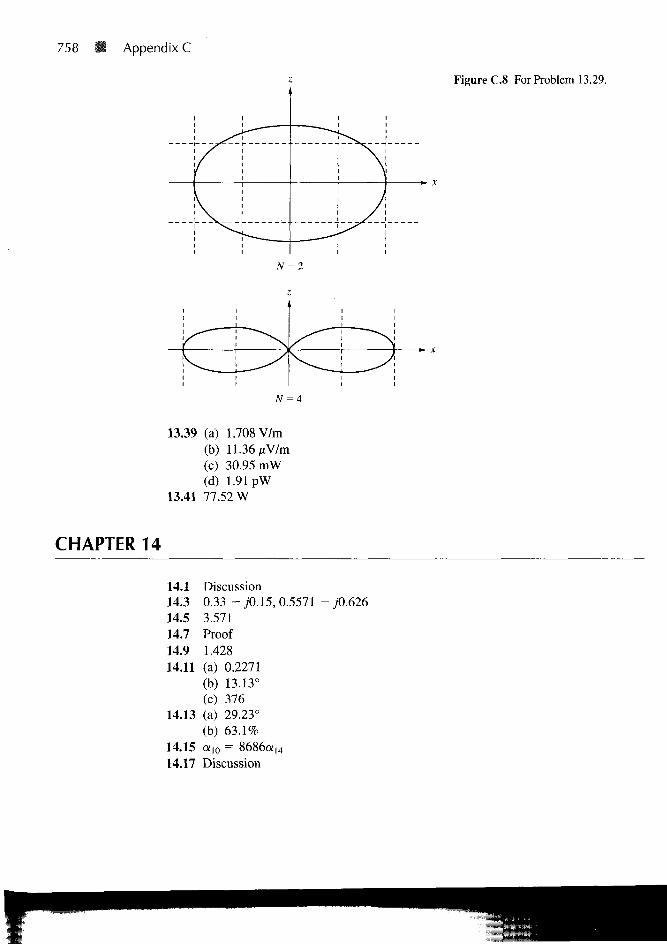
758 Appendix C
Figure C.8 For Problem 13.29.
N=l
N=4
13.39 (a) 1.708 V/m(b) 11.36|tiV/m(c) 30.95 mW(d) 1.91 pW
13.41 77.52 W
CHAPTER 14
14.114.314.514.714.914.11
14.13
14.1514.17
Discussion0.33 -yO. 15, 0.5571 - ;0.6263.571Proof1.428(a) 0.2271(b) 13.13°(c) 376(a) 29.23°(b) 63.1%aw = 8686a14
Discussion
APPENDIX C 759
CHAPTER 15
15.1 See Figure C.915.3 (a) 10.117, 1.56
(b) 10.113,1.50615.5 Proof15.7 6 V, 14 V15.9 V, = V2 = 37.5, V3 = V4 = 12.5
Figure C.9 For Problem 15.1.
760 Appendix C
15.11 (a) Matrix [A] remains the same, but -h2ps/s must be added to each termof matrix [B].
(b) Va = 4.276, Vb = 9.577, Vc = 11.126Vd = -2.013, Ve = 2.919, Vf = 6.069Vg = -3.424, Vh = -0.109, V; = 2.909
15.13 Numerical result agrees completely with the exact solution, e.g., for t = 0,V(0, 0) = 0, V(0.1, 0) = 0.3090, V(0.2, 0) = 0.5878, V(0.3, 0) = 0.809,V(0.4, 0) = 0.9511, V(0.5, 0) = 1.0, V(0.6, 0) = 0.9511, etc.
15.15 12.77 pF/m (numerical), 12.12 pF/m (exact)15.17 See Table C.3
TABLE C.3
6 (degrees)
10
203040
170
180
C(pF)
8.5483
9.06778.8938.606
11.32
8.6278
15.19 (a) Exact: C = 80.26 pF/m, Zo = 41.56 fi; for numerical solution, see Table C.4
TABLE C.4
N C (pF/m) Zo (ft)
10 82.386 40.48620 80.966 41.19740 80.438 41.467100 80.025 41.562
(b) For numerical results, see Table C.5
TABLE C.5
N C (PF/m) Zo (ft)
10 109.51 30.45820 108.71 30.68140 108.27 30.807
100 107.93 30.905
APPENDIX C 761
15.21 Proof15.23 (a) At (1.5, 0.5) along 12 and (0.9286, 0.9286) along 13.
(b) 56.67 V0 -0.6708
-1.2 -0.12481.408 -0.20815.25
0.8788-2.08
0-0.6708
15.27 18 V, 20 V15.29 See Table C.6
-0.2081.528
-1.2-0.1248 -0.208 1.0036
TABLE C.6
Node No.
8
9
10
1114
15
16
17
20
21
22
23
26
27
28
29
FEM
4.546
7.197
7.197
4.546
10.98
17.05
17.05
10.98
22.35
32.95
32.95
22.35
45.45
59.49
59.49
45.45
Exact
4.366
7.017
7.017
4.366
10.66
16.84
16.84
10.60
21.78
33.16
33.16
21.78
45.63
60.60
60.60
45.63
15.31 Proof

INDEX
Acceptance angle, 653Ac resistance, 427Ampere's law, 262, 273, 290
applications of, 274-278Amperian path, 274Amplitude, 412Angle of incidence, 451Angular frequency, 412Antenna pattern. See Radiation patternAntenna arrays, 612-618
binomial type, 621broadside type, 615end-fire type, 615
Antennas, 588-618types of, 589
Array factor, 613Attenuation, 649, 654Attenuation constant, 421, 479Azimuthal angle, 30
Bac-cab rule, 16Band matrix method, 672, 702Bandwidth, 638, 649Bessel differential equation, 223Biot-Savart's law, 262-266, 290, 307Bonding, 647Bonding effectiveness, 648Bounce diagram, 514Boundary conditions, 182-187, 330-332,
385Boundary-value problems, 199Brewster angle, 455
Capacitance, 224-230Capacitor, 224-230Cartesian coordinates, 29, 53Characteristic admittance, 480Characteristic impedance, 479, 525Charge conservation, 180Charged ring, 118Charged sphere, 128Circular cylindrical coordinates, 29, 55Circulation, 60
Closed form solution, 660Coaxial capacitor, 227Coaxial line, 276Colatitude, 33Complex permittivity, 422Complex variables, 728-729Components of a vector, 6Conductivity, 162, 164
values of, 737Conductors, 161, 164-167Conservation of magnetic flux, 283Conservative field, 87Constant-coordinates surfaces, 41^14Constitutive relations, 385Continuity equation, 180, 385Coulomb's law, 104-107, 305Critical angle, 653Cross product, 13Curie temperature, 328Curl, 75-80
definition of, 76properties of, 78
Current, 162-164conduction type, 164convection type, 163definition of, 162displacement type, 382
Current density,definition of, 163
Current reflection coefficient, 487Cutoff, 549Cutoff frequency, 542, 550Cutoff wavelength, 550
Dc resistance, 427, 647Definite integrals, 734Degenerate modes, 576Del operator, 63Derivatives, 731Diamagnetism, 327Dielectric breakdown, 175Dielectric constant, 175
values of, 738
Dielectric strength, 175Dielectrics, 161Difference equations, 669Differential displacement, 53, 55, 56, 89Differential normal area, 54, 55, 57, 89Differential solid angle, 606Differential volume, 54, 55, 57, 89Dipole antenna, 589Dipole moment, 143Directional derivative, 67Directive gain, 606Directivity, 606Dispersion, 654Displacement current density, 381Distance vector, 8Distortionless line, 481Divergence, 69-73
definition of, 69properties of, 72
Divergence theorem, 72, 125Dominant mode, 554, 578Dot product, 12
Effective area, 621Effective relative permittivity, 525Electric dipole, 142Electric displacement, 123Electric field intensity, 106Electric flux, 123Electric flux density, 122, 123Electric flux lines, 144Electric susceptibility, 174Electrical length, 486Electrohydrodynamic pump. 203Electromagnetic compatibility (EMC). 644Electromagnetic interference (EMI). 644Electromagnetics (EM), 3Electrometer, 179Electromotive force (emf), 370Electrostatic field, 103, 592Electrostatic shielding, 186Electrostatics, 103Element coefficient matrix, 698
763

764 Index
Emf. See Electromotive forceEnergy, 146, 339-341Equipotential line, 144Equipotential surface, 144Evanescent mode, 549Exponential identities, 730External inductance, 338
Far field, 592Faraday's law, 370Ferromagnetism, 328Field,
classification of, 86-88definition of, 5harmonic type, 84time-harmonic type, 389uniform type, 8
Field pattern, 604Field plotting, 661-663Filtering, 649Finite difference method, 669-674Finite element method, 694-703Finite elements, 694Five-node molecule, 672Fixed node, 670Force, 104, 304-308, 349Flux, 60Flux linkage, 336Free node, 670Frequency, 412Fresnel's equations, 455, 457Friss transmission formula, 623
Gauss's law, 124, 125, 283applications of, 126-130, 224-228
Gaussian surface, 126Global coefficient matrix, 699Gradient, 65-67Gradient operator, 63Grounding, 647Group pattern, 613Group velocity, 563
Half-wave dipole antenna, 594Helmholtz's equation, 419Helmholtz's theorem, 88Hertzian dipole, 590Homogeneous material, 175Hyperbolic functions, 729Hysteresis, 329
Indefinite integrals, 732-734Inductance, 336Inductive field, 592Inductor, 336Infinite line charge, 114, 127Infinite line current, 274
Infinite sheet of charge, 115, 128Infinite sheet of current, 275Input impedance, 484-486Insertion loss, 649Insulators, 161,162. See also DielectricsIntegral equation, 683Internal inductance, 338Intrinsic impedance, 420
of free space, 424Irrotational field, 87Isolated sphere, 228Isotropic antenna, 606Isotropic material, 175Iteration method, 672, 702
Joule's law, 167
Kernel, 683Kirchhoff's current law, 180, 348,478Kirchhoff 's voltage law, 477
Laplace's equation, 84, 199-202, 285,671,703
Laplacian, 83-85Lattice diagram. See Bounce diagramLenz'slaw, 371, 374Line charge, 112, 242Line integral, 60Linear material, 175Logarithmic identities, 730Lorentz condition, 388Lorentz force, 305, 314Lorentz force equation, 305, 384Loss angle, 422Loss tangent, 422Lossless line, 480Lossy dielectric, 418Lossy line, 480
Magnetic dipole, 318Magnetic dipole moment, 317Magnetic field intensity, 263, 281Magnetic flux density, 281Magnetic potentials, 284-287Magnetic susceptibility, 326Magnetization, 324Magnetization, 329Magnetization volume current density. 325Magnetization surface current density, 325Magnetomotive force, 347Magnetostatic field, 261Magnitude, 5Matched line, 489Maxwell's equations, 4, 125, 139, 182,
273, 283, 369-389, 418,438, 451,543, 545
Medium velocity, 563
Mesh size, 671Method of images, 240Microstrip lines, 524-526Microwave components, 639Microwaves, 638Mode, 546, 548Moment method, 683-687Monopole, 143Motional emf, 373Mutual inductance, 337
Newton's laws, 308Noise susceptibility, 649Nonmagnetic materials, 327Normalized impedance, 493Numerical aperture, 652
Ohm's law, 164, 166, 181,348Ohmic resistance, 608Open-circuited line, 489Optical fiber, 649
definition of, 650Orthogonal system, 28
Parallel-plate capacitor, 225, 226Paramagnetism, 327Pattern multiplication, 613Penetration depth. See Skin depthPeriod, 412Permeability, 326
of free space, 281Permeance, 348Permittivity, 175
of free space, 104Phase, 412Phase constant, 412,421,479Phase matching conditions, 452Phase velocity, 563Phasor, 389Plane of incidence, 451Point charge, 104, 126,241Poisson's equation, 199-202, 291, 670,
671,683Polarization, 171-174,425Polarization surface charge density, 173Polarization volume charge density, 173Position vector, 7, 106, 135, 451Potential, 134Potential difference, 133Power, 167,435^138Power gain, 607, 608Power pattern, 604Poynting's theorem, 436, 437Poynting vector, 436Pressure, 350
Propagation constant, 419, 479Propagation vector, 451

Quality factor, 578, 579Quarter-wave monopole antenna, 598Quarter-wave transformer, 505
Radar, 641,625types of, 627
Radar cross section, 626Radar range equation, 627Radar transmission equation, 627Radiated emissions, 644Radiation, 588Radiation efficiency, 608Radiation field, 592Radiation intensity, 605Radiation pattern, 604Radiation resistance, 593Reactance circle, 495Reflection coefficient, 442, 642, 643Refraction law, 185,332Refractive index, 453Relative permeability, 326
values of, 739Relative permittivity, 175. See also
Dielectric constantRelaxation time, 181, 229Reluctance, 348Resistance, 166, 223Resistance circle, 494Resistivity, 167Resonant frequency, 577Resultant pattern, 613Retarded potentials, 389Right-hand rule, 14, 80, 263, 372Right-hand screw rule, 80, 263
Satellite, 639Scalar, 5Scalar component, 16Scalar product, 12-15
Scattering cross section, 626Scattering parameters, 641Self-inductance, 336Semiconductor, 162Separation constant, 212, 221Separation of variables, 212, 221Shape functions, 696Shielding effectiveness, 648Shorted line, 489Single-stub tuner, 506Skin depth, 426Skin effect, 427Skin resistance, 428Slotted line, 507Small loop antenna, 599Smith chart, 492-498Snell's law, 453Solenoid, 271Solenoidal field, 87Spectrum, 415Spherical capacitor, 227Spherical coordinates, 32,56Standing wave, 442Standing wave ratio (SWR), 444Stokes's theorem, 79Superconductors, 162Superposition, 106, 135, 216Surface charge, 114Surface integral, 60
Tensor, 176Time-harmonic field, 389Torque, 316Total reflection, 653Transformation,
of point, 34of vector, 35
Transformer emf, 373Transient, 512Transmission coefficient, 442
Transmission line equaoccs. ~ —1~"-Transmission line parameters -I"-!—-~~Transmission lines, 473-526Transverse electric (TE) mode. 54".
552-556Transverse electromagnetic (TEM) wave.
425, 546Transverse magnetic (TM) mode, 547-551Trigonometric identities, 727-728
Uniform plane wave, 425Unit vector, 5, 6Uniqueness theorem, 201-202
Vector,addition of, 6definition of, 5multiplication of, 11subtraction of, 6
Vector component, 16Vector identities, 735Vector product, 13-15Voltage reflection coefficient, 486, 487Volume charge, 115Volume integral, 62
Wave, 410definition of, 411
Wave equation, 388, 411, 419, 479Wave number, 412Wave velocity, 411Waveguide resonator, 575Waveguide wavelength, 563Wavelength, 412Work done, 133
Xerographic copying machine, 204