p89v660/662/664 8-bit 80c51 5 v low power 16 kb/32 kb/64 ... · pca (programmable counter array)...
TRANSCRIPT
1. General description
The P89V660/662/664 are 80C51 microcontrollers with 16 kB/32 kB/64 kB flash and 512 B/1 kB/2 kB of data RAM. These devices are designed to be drop-in and software compatible replacements for the P89C660/662/664 devices. Both the In-System Programming (ISP) and In-Application Programming (IAP) boot codes are upward compatible.
Additional features of the P89V660/662/664 devices when compared to the P89C660/662/664 devices are the inclusion of a secondary 100 kHz byte-wide I2C-bus interface, an SPI interface, four addition I/O pins (Port 4), and the ability to erase code memory in 128-byte pages.
The IAP capability combined with the 128-byte page size allows for efficient use of the code memory for non-volatile data storage.
2. Features and benefits
2.1 Principal features
Dual 100 kHz byte-wide I2C-bus interfaces
128-byte page erase for efficient use of code memory as non-volatile data storage
0 MHz to 40 MHz operating frequency in 12x mode, 20 MHz in 6x mode
16 kB/32 kB/64 kB of on-chip flash user code memory with ISP and IAP
512 B/1 kB/2 kB RAM
SPI (Serial Peripheral Interface) and enhanced UART
PCA (Programmable Counter Array) with PWM and Capture/Compare functions
Three 16-bit timers/counters
Four 8-bit I/O ports, one 4-bit I/O port
WatchDog Timer (WDT)
2.2 Additional features
30 ms page erase, 150 ms block erase
Support for 6-clock (default) or 12-clock mode selection via ISP or parallel programmer
PLCC44 and TQFP44 packages
Ten interrupt sources with four priority levels
Second DPTR register
Low EMI mode (ALE inhibit)
Power-down mode with external interrupt wake-up
P89V660/662/6648-bit 80C51 5 V low power 16 kB/32 kB/64 kB flash microcontroller with 512 B/1 kB/2 kB RAM, dual I2C-bus, SPIRev. 3.1 — 17 October 2011 Product data sheet

NXP Semiconductors P89V660/662/66480C51 with 512 B/1 kB/2 kB RAM, dual I2C-bus, SPI
Idle mode
2.3 Comparison to the P89C660/662/664 devices
SPI interface. The P89V660/662/664 devices include an SPI interface that was not present on the P89C660/662/664 devices.
Dual I2C-bus interfaces. The P89V660/662/664 devices have two I2C-bus interfaces. The P89C660/662/664 devices have one.
More I/O pins. The P89V660/662/664 devices have an additional four-bit I/O port, Port 4.
The 6x/12x mode on theP89V660/662/664 devices is programmable and erasable using ISP and IAP as well as parallel programmer mode. The P89C660/662/664 devices could only be switched using parallel programmer mode.
Smaller block sizes. The smallest block size on the P89C660/662/664 devices was 8 kB. The P89V660/662/664 devices have a page size of 128 B. These small pages can be erased and reprogrammed using IAP function calls making use of the code memory for non-volatile data storage practical. Each page erase is 30 ms or less. The IAP and ISP code in P89V660/662/664 devices support these 128-byte page operations. In addition, the IAP and ISP code uses multiple page erase operations to emulate the erasing of the larger block sizes (8 kB and 16 kB to maintain firmware compatibility).
Status bit versus Status byte. The P89V660/662/664 devices used a Status byte to control the automatic entry into ISP mode following a reset. On the P89V660/662/664 devices this has changed to a single Status bit. Since the ISP entry was based on the zero/non-zero value of the Status byte this is an almost identical operation on the P89V660/662/664 devices.
Faster block erase. The erase time for the entire user code memory of the P89V660/662/664 devices is 150 ms.
3. Ordering information
Table 1. Ordering information
Type number Package
Name Description Version
P89V662FA PLCC44 plastic leaded chip carrier; 44 leads SOT187-2
P89V662FBC TQFP44 plastic thin quad flat package; 44 leads; body 10 10 1.0 mm
SOT376-1
P89V664FA PLCC44 plastic leaded chip carrier; 44 leads SOT187-2
P89V664FBC TQFP44 plastic thin quad flat package; 44 leads; body 10 10 1.0 mm
SOT376-1
P89V660_662_664 All information provided in this document is subject to legal disclaimers. © NXP B.V. 2011. All rights reserved.
Product data sheet Rev. 3.1 — 17 October 2011 2 of 90
NXP Semiconductors P89V660/662/66480C51 with 512 B/1 kB/2 kB RAM, dual I2C-bus, SPI
3.1 Ordering options
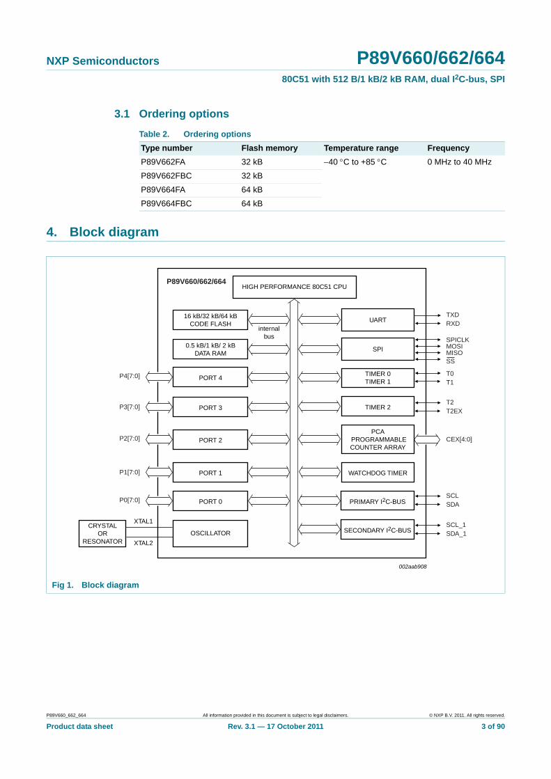
4. Block diagram
Table 2. Ordering options
Type number Flash memory Temperature range Frequency
P89V662FA 32 kB 40 C to +85 C 0 MHz to 40 MHz
P89V662FBC 32 kB
P89V664FA 64 kB
P89V664FBC 64 kB
Fig 1. Block diagram
HIGH PERFORMANCE 80C51 CPU
16 kB/32 kB/64 kBCODE FLASH
0.5 kB/1 kB/ 2 kBDATA RAM
PORT 2
PORT 1
PORT 0
OSCILLATOR
internalbus
CRYSTALOR
RESONATOR
002aab908
UART
PCA PROGRAMMABLECOUNTER ARRAY
PORT 3 TIMER 2
TIMER 0TIMER 1
SPI
XTAL1
XTAL2
PRIMARY I2C-BUS
WATCHDOG TIMER
SECONDARY I2C-BUS
PORT 4P4[7:0]
P3[7:0]
P2[7:0]
P1[7:0]
P0[7:0]
TXDRXD
T0
SPICLKMOSIMISOSS
T1
T2T2EX
SCLSDA
SCL_1SDA_1
CEX[4:0]
P89V660/662/664
P89V660_662_664 All information provided in this document is subject to legal disclaimers. © NXP B.V. 2011. All rights reserved.
Product data sheet Rev. 3.1 — 17 October 2011 3 of 90
NXP Semiconductors P89V660/662/66480C51 with 512 B/1 kB/2 kB RAM, dual I2C-bus, SPI
5. Pinning information
5.1 Pinning
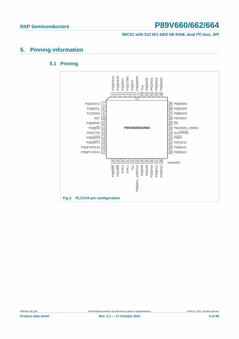
Fig 2. PLCC44 pin configuration
P89V660/662/664
P1[5]/CEX2 P0[4]/AD4
P1[6]/SCL P0[5]/AD5
P1[7]/SDA P0[6]/AD6
RST P0[7]/AD7
P3[0]/RXD
P4[1]/SDA_1/MISO
P3[1]/TXD
P2[7]/A15
P3[4]/T0/CEX3 P2[6]/A14
P3[5]/T1/CEX4 P2[5]/A13
P1[
4]/C
EX
1
P1[
3]/C
EX
0
XTA
L2P
1[2]
/EC
I
XTA
L1P
1[1]
/T2E
X
VS
SP
1[0]
/T2
P4[
0]/S
CL_
1/S
PIC
LKP
4[2]
/MO
SI
P2[
0]/A
8V
DD
P2[
1]/A
9P
0[0]
/AD
0
P2[
2]/A
10P
0[1]
/AD
1
P2[
3]/A
11P
0[2]
/AD
2
P2[
4]/A
12P
0[3]
/AD
3002aab909
7
8
9
10
11
12
13
14
15
16
17
39
38
37
36
35
34
33
32
31
30
29
18 19 20 21 22 23 24 25 26 27 28
6 5 4 3 2 1 44 43 42 41 40
EA
ALE/PROG
PSEN
P3[
6]/W
R
P3[
7]/R
D
P3[3]/INT1
P3[2]/INT0
P4[3]/SS
P89V660_662_664 All information provided in this document is subject to legal disclaimers. © NXP B.V. 2011. All rights reserved.
Product data sheet Rev. 3.1 — 17 October 2011 4 of 90
NXP Semiconductors P89V660/662/66480C51 with 512 B/1 kB/2 kB RAM, dual I2C-bus, SPI
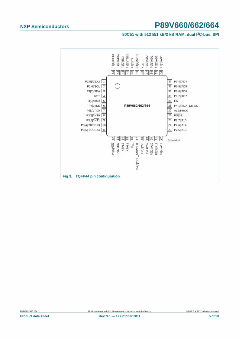
Fig 3. TQFP44 pin configuration
P89V660/662/664
P1[5]/CEX2 P0[4]/AD4
P1[6]/SCL P0[5]/AD5
P1[7]/SDA P0[6]/AD6
RST P0[7]/AD7
P3[0]/RXD
P4[1]/SDA_1/MISO
P3[1]/TXD
P2[7]/A15
P3[4]/T0/CEX3 P2[6]/A14
P3[5]/T1/CEX4 P2[5]/A13
P1[
4]/C
EX
1
P1[
3]/C
EX
0
XTA
L2P
1[2]
/EC
I
XTA
L1P
1[1]
/T2E
X
VS
SP
1[0]
/T2
P4[
0]/S
CL_
1/S
PIC
LKP
4[2]
/MO
SI
P2[
0]/A
8V
DD
P2[
1]/A
9P
0[0]
/AD
0
P2[
2]/A
10P
0[1]
/AD
1
P2[
3]/A
11P
0[2]
/AD
2
P2[
4]/A
12P
0[3]
/AD
3
002aab910
EA
ALE/PROG
PSENP
3[6]
/WR
P3[
7]/R
DP3[3]/INT1
P3[2]/INT0
P4[3]/SS
1
2
3
4
5
6
7
8
9
10
11
33
32
31
30
29
28
27
26
25
24
23
12 13 14 15 16 17 18 19 20 21 22
44 43 42 41 40 39 38 37 36 35 34
P89V660_662_664 All information provided in this document is subject to legal disclaimers. © NXP B.V. 2011. All rights reserved.
Product data sheet Rev. 3.1 — 17 October 2011 5 of 90

NXP Semiconductors P89V660/662/66480C51 with 512 B/1 kB/2 kB RAM, dual I2C-bus, SPI
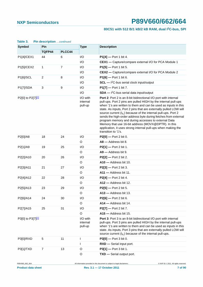
5.2 Pin description
Table 3. Pin description
Symbol Pin Type Description
TQFP44 PLCC44
P0[0] to P0[7] I/O Port 0: Port 0 is an 8-bit open-drain bidirectional I/O port. Port 0 pins that have ‘1’s written to them float, and in this state can be used as high-impedance inputs. Port 0 is also the multiplexed low-order address and data bus during accesses to external code and data memory. In this application, it uses strong internal pull-ups when making the transition to ‘1’s. External pull-ups are required as a general purpose I/O port.
P0[0]/AD0 37 43 I/O P0[0] — Port 0 bit 0.
I/O AD0 — Address/data bit 0.
P0[1]/AD1 36 42 I/O P0[1] — Port 0 bit 1.
I/O AD1 — Address/data bit 1.
P0[2]/AD2 35 41 I/O P0[2] — Port 0 bit 2.
I/O AD2 — Address/data bit 2.
P0[3]/AD3 34 40 I/O P0[3] — Port 0 bit 3.
I/O AD3 — Address/data bit 3.
P0[4]/AD4 33 39 I/O P0[4] — Port 0 bit 4.
I/O AD4 — Address/data bit 4.
P0[5]/AD5 32 38 I/O P0[5] — Port 0 bit 5.
I/O AD5 — Address/data bit 5.
P0[6]/AD6 31 37 I/O P0[6] — Port 0 bit 6.
I/O AD6 — Address/data bit 6.
P0[7]/AD7 30 36 I/O P0[7] — Port 0 bit 7.
I/O AD7 — Address/data bit 7.
P1[0] to P1[7][1] I/O with internal pull-up
Port 1: Port 1 is an 8-bit bidirectional I/O port with internal pull-ups. The Port 1 pins are pulled high by the internal pull-ups when ‘1’s are written to them and can be used as inputs in this state. As inputs, Port 1 pins that are externally pulled LOW will source current (IIL) because of the internal pull-ups. P1[5], P1[6], P1[7] have high current drive of 16 mA.
P1[0]/T2 40 2 I/O P1[0] — Port 1 bit 0.
I T2 — External count input to Timer/Counter 2 or Clock-out from Timer/Counter 2
P1[1]/T2EX 41 3 I/O P1[1] — Port 1 bit 1.
I T2EX: Timer/Counter 2 capture/reload trigger and direction control
P1[2]/ECI 42 4 I/O P1[2] — Port 1 bit 2.
I ECI — External clock input. This signal is the external clock input for the PCA.
P1[3]/CEX0 43 5 I/O P1[3] — Port 1 bit 3.
I/O CEX0 — Capture/compare external I/O for PCA Module 0. Each capture/compare module connects to a Port 1 pin for external I/O. When not used by the PCA, this pin can handle standard I/O.
P89V660_662_664 All information provided in this document is subject to legal disclaimers. © NXP B.V. 2011. All rights reserved.
Product data sheet Rev. 3.1 — 17 October 2011 6 of 90
NXP Semiconductors P89V660/662/66480C51 with 512 B/1 kB/2 kB RAM, dual I2C-bus, SPI
P1[4]/CEX1 44 6 I/O P1[4] — Port 1 bit 4.
I/O CEX1 — Capture/compare external I/O for PCA Module 1
P1[5]/CEX2 1 7 I/O P1[5] — Port 1 bit 5.
I/O CEX2 — Capture/compare external I/O for PCA Module 2
P1[6]/SCL 2 8 I/O P1[6] — Port 1 bit 6.
I/O SCL — I2C-bus serial clock input/output
P1[7]/SDA 3 9 I/O P1[7] — Port 1 bit 7.
I/O SDA — I2C-bus serial data input/output
P2[0] to P2[7][1] I/O with internal pull-up
Port 2: Port 2 is an 8-bit bidirectional I/O port with internal pull-ups. Port 2 pins are pulled HIGH by the internal pull-ups when ‘1’s are written to them and can be used as inputs in this state. As inputs, Port 2 pins that are externally pulled LOW will source current (IIL) because of the internal pull-ups. Port 2 sends the high-order address byte during fetches from external program memory and during accesses to external Data Memory that use 16-bit address (MOVX@DPTR). In this application, it uses strong internal pull-ups when making the transition to ‘1’s.
P2[0]/A8 18 24 I/O P2[0] — Port 2 bit 0.
O A8 — Address bit 8.
P2[1]/A9 19 25 I/O P2[1] — Port 2 bit 1.
O A9 — Address bit 9.
P2[2]/A10 20 26 I/O P2[2] — Port 2 bit 2.
O A10 — Address bit 10.
P2[3]/A11 21 27 I/O P2[3] — Port 2 bit 3.
O A11 — Address bit 11.
P2[4]/A12 22 28 I/O P2[4] — Port 2 bit 4.
O A12 — Address bit 12.
P2[5]/A13 23 29 I/O P2[5] — Port 2 bit 5.
O A13 — Address bit 13.
P2[6]/A14 24 30 I/O P2[6] — Port 2 bit 6.
O A14 — Address bit 14.
P2[7]/A15 25 31 I/O P2[7] — Port 2 bit 7.
O A15 — Address bit 15.
P3[0] to P3[7][1] I/O with internal pull-up
Port 3: Port 3 is an 8-bit bidirectional I/O port with internal pull-ups. Port 3 pins are pulled HIGH by the internal pull-ups when ‘1’s are written to them and can be used as inputs in this state. As inputs, Port 3 pins that are externally pulled LOW will source current (IIL) because of the internal pull-ups.
P3[0]/RXD 5 11 I P3[0] — Port 3 bit 0.
I RXD — Serial input port.
P3[1]/TXD 7 13 O P3[1] — Port 3 bit 1.
O TXD — Serial output port.
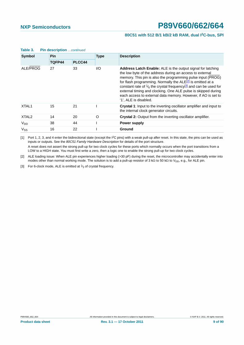
Table 3. Pin description …continued
Symbol Pin Type Description
TQFP44 PLCC44
P89V660_662_664 All information provided in this document is subject to legal disclaimers. © NXP B.V. 2011. All rights reserved.
Product data sheet Rev. 3.1 — 17 October 2011 7 of 90

NXP Semiconductors P89V660/662/66480C51 with 512 B/1 kB/2 kB RAM, dual I2C-bus, SPI
P3[2]/INT0 8 14 I P3[2] — Port 3 bit 2.
I INT0 — External interrupt 0 input.
P3[3]/INT1 9 15 I P3[3] — Port 3 bit 3.
I INT1 — External interrupt 1 input
P3[4]/T0/CEX3 10 16 I/O P3[4] — Port 3 bit 4.
I T0 — External count input to Timer/Counter 0.
I/O CEX3 — Capture/compare external I/O for PCA Module 3.
P3[5]/T1/CEX4 11 17 I/O P3[5] — Port 3 bit 5.
I T1 — External count input to Timer/Counter 1
I/O CEX4 — Capture/compare external I/O for PCA Module 4
P3[6]/WR 12 18 O P3[6] — Port 3 bit 6.
O WR — External data memory write strobe
P3[7]/RD 13 19 O P3[7] — Port 3 bit 7.
O RD — External data memory read strobe.
P4[0] to P4[3][1] I/O with internal pull-up
Port 4: Port 4 is a 4-bit bidirectional I/O port with internal pull-ups. Port 4 pins are pulled HIGH by the internal pull-ups when ‘1’s are written to them and can be used as inputs in this state. As inputs, Port 4 pins that are externally pulled LOW will source current (IIL) because of the internal pull-ups.
P4[0]/SCL_1/SPICLK
17 23 I/O P4[0] — Port 4 bit 0.
I/O SCL_1 — Second I2C-bus serial clock input/output
I/O SPICLK — Serial clock input/output for SPI
P4[1]/SDA_1/MISO
28 34 I/O P4[1] — Port 4 bit 1.
I/O SDA_1 — Second I2C-bus serial data input/output
I/O MISO — Master input/slave output for SPI
P4[2]/MOSI 39 1 I/O P4[2] — Port 4 bit 2.
I/O MOSI — Master output/slave input for SPI
P4[3]/SS 6 12 I P4[3] — Port 4 bit 3.
I SS — Slave select input for SPI
PSEN 26 32 I/O Program Store Enable: PSEN is the read strobe for external program memory. When the device is executing from internal program memory, PSEN is inactive (HIGH). When the device is executing code from external program memory, PSEN is activated twice each machine cycle, except that two PSEN activations are skipped during each access to external data memory.
RST 4 10 I Reset: While the oscillator is running, a HIGH logic state on this pin for two machine cycles will reset the device.
EA 29 35 I External Access Enable: EA must be connected to VSS in order to enable the device to fetch code from the external program memory. EA must be strapped to VDD for internal program execution.
Table 3. Pin description …continued
Symbol Pin Type Description
TQFP44 PLCC44
P89V660_662_664 All information provided in this document is subject to legal disclaimers. © NXP B.V. 2011. All rights reserved.
Product data sheet Rev. 3.1 — 17 October 2011 8 of 90
NXP Semiconductors P89V660/662/66480C51 with 512 B/1 kB/2 kB RAM, dual I2C-bus, SPI
[1] Port 1, 2, 3, and 4 enter the bidirectional state (except the I2C pins) with a weak pull-up after reset. In this state, the pins can be used as inputs or outputs. See the 80C51 Family Hardware Description for details of the port structure.
A reset does not assert the strong pull-up for two clock cycles for these ports which normally occurs when the port transitions from a LOW to a HIGH state. You must first write a zero, then a logic one to enable the strong pull-up for two clock cycles.
[2] ALE loading issue: When ALE pin experiences higher loading (>30 pF) during the reset, the microcontroller may accidentally enter into modes other than normal working mode. The solution is to add a pull-up resistor of 3 k to 50 k to VDD, e.g., for ALE pin.
[3] For 6-clock mode, ALE is emitted at 1⁄3 of crystal frequency.
ALE/PROG 27 33 I/O Address Latch Enable: ALE is the output signal for latching the low byte of the address during an access to external memory. This pin is also the programming pulse input (PROG) for flash programming. Normally the ALE[2] is emitted at a constant rate of 1⁄6 the crystal frequency[3] and can be used for external timing and clocking. One ALE pulse is skipped during each access to external data memory. However, if AO is set to ‘1’, ALE is disabled.
XTAL1 15 21 I Crystal 1: Input to the inverting oscillator amplifier and input to the internal clock generator circuits.
XTAL2 14 20 O Crystal 2: Output from the inverting oscillator amplifier.
VDD 38 44 I Power supply
VSS 16 22 I Ground
Table 3. Pin description …continued
Symbol Pin Type Description
TQFP44 PLCC44
P89V660_662_664 All information provided in this document is subject to legal disclaimers. © NXP B.V. 2011. All rights reserved.
Product data sheet Rev. 3.1 — 17 October 2011 9 of 90
NXP Semiconductors P89V660/662/66480C51 with 512 B/1 kB/2 kB RAM, dual I2C-bus, SPI
6. Functional description
6.1 Special function registers
Remark: SFR accesses are restricted in the following ways:
• User must not attempt to access any SFR locations not defined.
• Accesses to any defined SFR locations must be strictly for the functions for the SFRs.
• SFR bits labeled ‘-’, ‘0’ or ‘1’ can only be written and read as follows:
– ‘-’ Unless otherwise specified, must be written with ‘0’, but can return any value when read (even if it was written with ‘0’). It is a reserved bit and may be used in future derivatives.
– ‘0’ must be written with ‘0’, and will return a ‘0’ when read.
– ‘1’ must be written with ‘1’, and will return a ‘1’ when read.
P89V660_662_664 All information provided in this document is subject to legal disclaimers. © NXP B.V. 2011. All rights reserved.
Product data sheet Rev. 3.1 — 17 October 2011 10 of 90

xxxxxxxxxxxxxxxxxxxxx xxxxxxxxxxxxxxxxxxxxxxxxxx xxxxxxx x x x xxxxxxxxxxxxxxxxxxxxxxxxxxxxxx xxxxxxxxxxxxxxxxxxx xx xx xxxxx xxxxxxxxxxxxxxxxxxxxxxxxxxx xxxxxxxxxxxxxxxxxxx xxxxxx xxxxxxxxxxxxxxxxxxxxxxxxxxxxxxxxxxx xxxxxxxxxxxx x x xxxxxxxxxxxxxxxxxxxxx xxxxxxxxxxxxxxxxxxxxxxxxxxxxxx xxxxx xxxxxxxxxxxxxxxxxxxxxxxxxxxxxxxxxxxxxxxxxxxxxxxxxx xxxxxxxx xxxxxxxxxxxxxxxxxxxxxxxxx xxxxxxxxxxxxxxxxxxxx xxx
P8
9V66
0_662_66
4
Pro
du
ct data sh
NX
P S
emico
nd
ucto
rsP
89V660/662/664
80C
51 w
ith 51
2 B/1
kB
/2 k
B R
AM
, du
al I 2C
-bu
s, SP
I
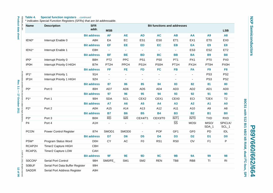
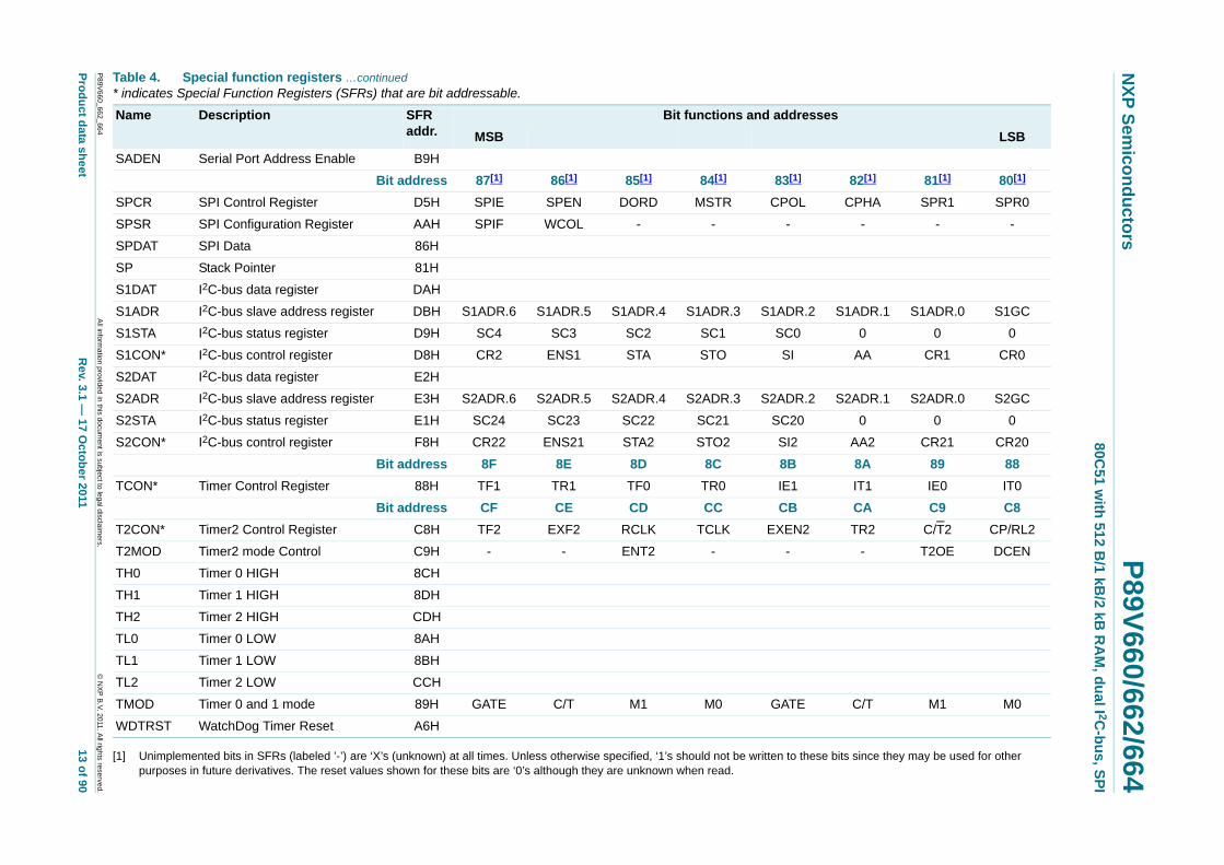
Table 4. Special function registers* indicates Special Function Registers (SFRs) that are bit addressable.
Name Description SFR addr.
Bit functions and addresses
MSB LSB
E2 E1 E0
- EXTRAM AO
0 - DPS
F2 F1 F0
TOG_0 PWM_0 ECCF_0
TOG_1 PWM_1 ECCF_1
TOG_2 PWM_2 ECCF_2
TOG_3 PWM_3 ECCF_3
TOG_4 PWM_4 ECCF_4
DA D9 D8
CCF2 CCF1 CCF0
CPS1 CPS0 ECF
All inform
ation provided
in this docum
ent is subject to leg
al disclaim
ers.©
NX
P B
.V. 2011. A
ll rights reserved.
eetR
ev. 3.1 —
17 O
ctob
er 2011 11 o
f 90
Bit address E7 E6 E5 E4 E3
ACC* Accumulator E0H
AUXR Auxiliary function register 8EH - - - - -
AUXR1 Auxiliary function register 1 A2H - - - GF2
Bit address F7 F6 F5 F4 F3
B* B register F0H
CCAP0H Module 0 Capture HIGH FAH
CCAP1H Module 1 Capture HIGH FBH
CCAP2H Module 2 Capture HIGH FCH
CCAP3H Module 3 Capture HIGH FDH
CCAP4H Module 4 Capture HIGH FEH
CCAP0L Module 0 Capture LOW EAH
CCAP1L Module 1 Capture LOW EBH
CCAP2L Module 2 Capture LOW ECH
CCAP3L Module 3 Capture LOW EDH
CCAP4L Module 4 Capture LOW EEH
CCAPM0 Module 0 mode C2H - ECOM_0 CAPP_0 CAPN_0 MAT_0
CCAPM1 Module 1 mode C3H - ECOM_1 CAPP_1 CAPN_1 MAT_1
CCAPM2 Module 2 mode C4H - ECOM_2 CAPP_2 CAPN_2 MAT_2
CCAPM3 Module 3 mode C5H - ECOM_3 CAPP_3 CAPN_3 MAT_3
CCAPM4 Module 4 mode C6H - ECOM_4 CAPP_4 CAPN_4 MAT_4
Bit address DF DE DD DC DB
CCON* PCA Counter Control C0H CF CR - CCF4 CCF3
CH PCA Counter HIGH F9H
CL PCA Counter LOW E9H
CMOD PCA Counter mode C1H CIDL WDTE - - -
DPTR Data Pointer (2 B)
DPH Data Pointer HIGH 83H
DPL Data Pointer LOW 82H
xxxxxxxxxxxxxxxxxxxxx xxxxxxxxxxxxxxxxxxxxxxxxxx xxxxxxx x x x xxxxxxxxxxxxxxxxxxxxxxxxxxxxxx xxxxxxxxxxxxxxxxxxx xx xx xxxxx xxxxxxxxxxxxxxxxxxxxxxxxxxx xxxxxxxxxxxxxxxxxxx xxxxxx xxxxxxxxxxxxxxxxxxxxxxxxxxxxxxxxxxx xxxxxxxxxxxx x x xxxxxxxxxxxxxxxxxxxxx xxxxxxxxxxxxxxxxxxxxxxxxxxxxxx xxxxx xxxxxxxxxxxxxxxxxxxxxxxxxxxxxxxxxxxxxxxxxxxxxxxxxx xxxxxxxx xxxxxxxxxxxxxxxxxxxxxxxxx xxxxxxxxxxxxxxxxxxxx xxx
P8
9V66
0_662_66
4
Pro
du
ct data sh
NX
P S
emico
nd
ucto
rsP
89V660/662/664
80C
51 w
ith 51
2 B/1
kB
/2 k
B R
AM
, du
al I 2C
-bu
s, SP
I
AA A9 A8
EX1 ET0 EX0
EA E9 E8
ES3 ES2 ET2
BA B9 B8
PX1 PT0 PX0
PX1H PT0H PX0H
FA F9 F8
- PS3 PS2
- PS3 PS2
82 81 80
AD2 AD1 AD0
92 91 90
ECI T2EX T2
A2 A1 A0
A10 A9 A8
B2 B1 B0
INT0 TXD RXD
MOSI MISO/SDA_1
SPICLK/SCL_1
GF0 PD IDL
D2 D1 D0
OV F1 P
9A 99 98
RB8 TI RI
Table 4. Special function registers …continued* indicates Special Function Registers (SFRs) that are bit addressable.
Name Description SFR addr.
Bit functions and addresses
MSB LSB
All inform
ation provided
in this docum
ent is subject to leg
al disclaim
ers.©
NX
P B
.V. 2011. A
ll rights reserved.
eetR
ev. 3.1 —
17 O
ctob
er 2011 12 o
f 90
Bit address AF AE AD AC AB
IEN0* Interrupt Enable 0 A8H EA EC ES1 ES0 ET1
Bit address EF EE ED EC EB
IEN1* Interrupt Enable 1 E8H - - - - -
Bit address BF BE BD BC BB
IP0* Interrupt Priority 0 B8H PT2 PPC PS1 PS0 PT1
IP0H Interrupt Priority 0 HIGH B7H PT2H PPCH PS1H PS0H PT1H
Bit address FF FE FD FC FB
IP1* Interrupt Priority 1 91H - - - - -
IP1H Interrupt Priority 1 HIGH 92H - - - - -
Bit address 87 86 85 84 83
P0* Port 0 80H AD7 AD6 AD5 AD4 AD3
Bit address 97 96 95 94 93
P1* Port 1 90H SDA SCL CEX2 CEX1 CEX0
Bit address A7 A6 A5 A4 A3
P2* Port 2 A0H A15 A14 A13 A12 A11
Bit address B7 B6 B5 B4 B3
P3* Port 3 B0H RD WR CEX4/T1 CEX3/T0 INT1
P4 Port 4 A1H - - - - SS
PCON Power Control Register 87H SMOD1 SMOD0 - POF GF1
Bit address D7 D6 D5 D4 D3
PSW* Program Status Word D0H CY AC F0 RS1 RS0
RCAP2H Timer2 Capture HIGH CBH
RCAP2L Timer2 Capture LOW CAH
Bit address 9F 9E 9D 9C 9B
S0CON* Serial Port Control 98H SM0/FE_ SM1 SM2 REN TB8
S0BUF Serial Port Data Buffer Register 99H
SADDR Serial Port Address Register A9H
xxxxxxxxxxxxxxxxxxxxx xxxxxxxxxxxxxxxxxxxxxxxxxx xxxxxxx x x x xxxxxxxxxxxxxxxxxxxxxxxxxxxxxx xxxxxxxxxxxxxxxxxxx xx xx xxxxx xxxxxxxxxxxxxxxxxxxxxxxxxxx xxxxxxxxxxxxxxxxxxx xxxxxx xxxxxxxxxxxxxxxxxxxxxxxxxxxxxxxxxxx xxxxxxxxxxxx x x xxxxxxxxxxxxxxxxxxxxx xxxxxxxxxxxxxxxxxxxxxxxxxxxxxx xxxxx xxxxxxxxxxxxxxxxxxxxxxxxxxxxxxxxxxxxxxxxxxxxxxxxxx xxxxxxxx xxxxxxxxxxxxxxxxxxxxxxxxx xxxxxxxxxxxxxxxxxxxx xxx
P8
9V66
0_662_66
4
Pro
du
ct data sh
NX
P S
emico
nd
ucto
rsP
89V660/662/664
80C
51 w
ith 51
2 B/1
kB
/2 k
B R
AM
, du
al I 2C
-bu
s, SP
I
ese bits since they may be used for other
82[1] 81[1] 80[1]
CPHA SPR1 SPR0
- - -
2 S1ADR.1 S1ADR.0 S1GC
0 0 0
AA CR1 CR0
2 S2ADR.1 S2ADR.0 S2GC
0 0 0
AA2 CR21 CR20
8A 89 88
IT1 IE0 IT0
CA C9 C8
TR2 C/T2 CP/RL2
- T2OE DCEN
C/T M1 M0
Table 4. Special function registers …continued* indicates Special Function Registers (SFRs) that are bit addressable.
Name Description SFR addr.
Bit functions and addresses
MSB LSB
All inform
ation provided
in this docum
ent is subject to leg
al disclaim
ers.©
NX
P B
.V. 2011. A
ll rights reserved.
eetR
ev. 3.1 —
17 O
ctob
er 2011 13 o
f 90
[1] Unimplemented bits in SFRs (labeled ’-’) are ‘X’s (unknown) at all times. Unless otherwise specified, ‘1’s should not be written to thpurposes in future derivatives. The reset values shown for these bits are ‘0’s although they are unknown when read.
SADEN Serial Port Address Enable B9H
Bit address 87[1] 86[1] 85[1] 84[1] 83[1]
SPCR SPI Control Register D5H SPIE SPEN DORD MSTR CPOL
SPSR SPI Configuration Register AAH SPIF WCOL - - -
SPDAT SPI Data 86H
SP Stack Pointer 81H
S1DAT I2C-bus data register DAH
S1ADR I2C-bus slave address register DBH S1ADR.6 S1ADR.5 S1ADR.4 S1ADR.3 S1ADR.
S1STA I2C-bus status register D9H SC4 SC3 SC2 SC1 SC0
S1CON* I2C-bus control register D8H CR2 ENS1 STA STO SI
S2DAT I2C-bus data register E2H
S2ADR I2C-bus slave address register E3H S2ADR.6 S2ADR.5 S2ADR.4 S2ADR.3 S2ADR.
S2STA I2C-bus status register E1H SC24 SC23 SC22 SC21 SC20
S2CON* I2C-bus control register F8H CR22 ENS21 STA2 STO2 SI2
Bit address 8F 8E 8D 8C 8B
TCON* Timer Control Register 88H TF1 TR1 TF0 TR0 IE1
Bit address CF CE CD CC CB
T2CON* Timer2 Control Register C8H TF2 EXF2 RCLK TCLK EXEN2
T2MOD Timer2 mode Control C9H - - ENT2 - -
TH0 Timer 0 HIGH 8CH
TH1 Timer 1 HIGH 8DH
TH2 Timer 2 HIGH CDH
TL0 Timer 0 LOW 8AH
TL1 Timer 1 LOW 8BH
TL2 Timer 2 LOW CCH
TMOD Timer 0 and 1 mode 89H GATE C/T M1 M0 GATE
WDTRST WatchDog Timer Reset A6H

NXP Semiconductors P89V660/662/66480C51 with 512 B/1 kB/2 kB RAM, dual I2C-bus, SPI
6.2 Memory organization
The various P89V660/662/664 memory spaces are as follows:
• DATA
128 B of internal data memory space (00H:7FH) accessed via direct or indirect addressing, using instructions other than MOVX and MOVC. All or part of the Stack may be in this area.
• IDATA
Indirect Data. 256 B of internal data memory space (00H:FFH) accessed via indirect addressing using instructions other than MOVX and MOVC. All or part of the Stack may be in this area. This area includes the DATA area and the 128 B immediately above it.
• SFR
Special Function Registers. Selected CPU registers and peripheral control and status registers, accessible only via direct addressing.
• XDATA
‘External’ Data or Auxiliary RAM. Duplicates the classic 80C51 64 kB memory space addressed via the MOVX instruction using the DPTR, R0, or R1. The P89V660/662/664 have 256/768/1792 B of on-chip XDATA memory.
• CODE
64 kB of Code memory space, accessed as part of program execution and via the MOVC instruction. The P89V660/662/664 have 16/32/64 kB of on-chip Code memory.
6.2.1 Expanded data RAM addressing
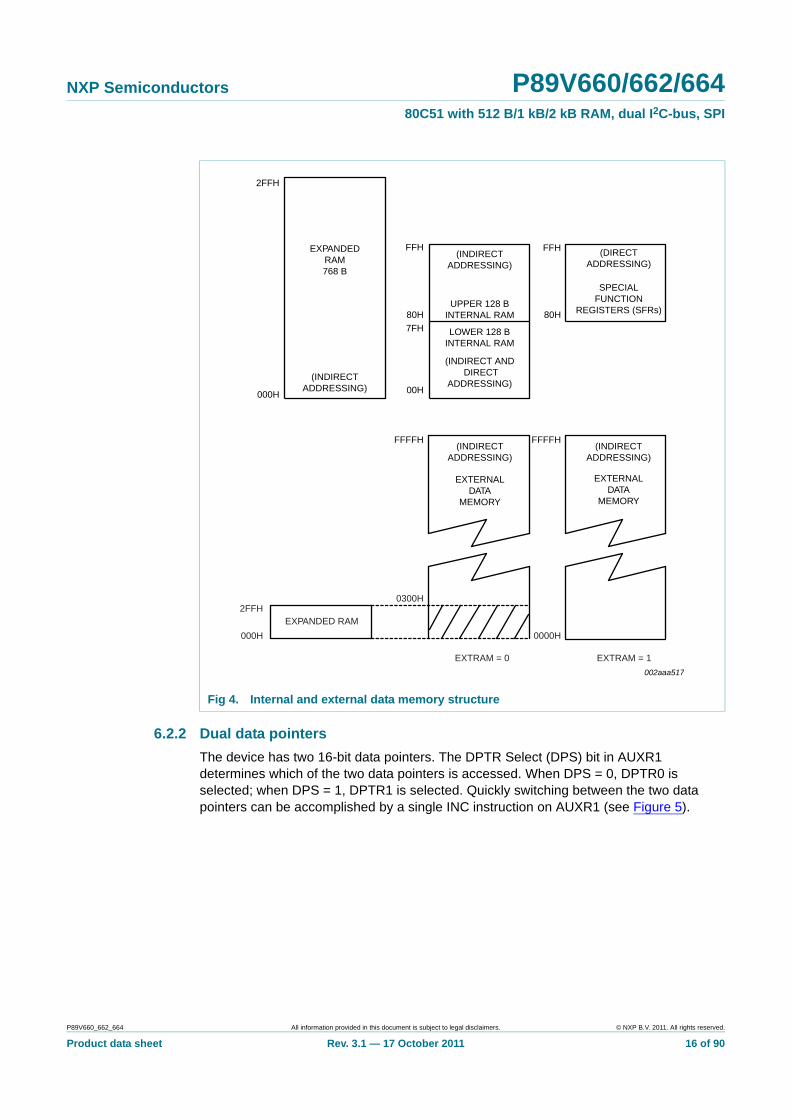
The P89V660/662/664 have 512 B/1 kB/2 kB of RAM. See Figure 4.
To access the expanded RAM, the EXTRAM bit must be set and MOVX instructions must be used. The extra memory is physically located on the chip and logically occupies the first bytes of external memory (addresses 000H to 0FFH/2FFH/6FFH).
When EXTRAM = 1, the expanded RAM is indirectly addressed using the MOVX instruction in combination with any of the registers R0, R1 of the selected bank or DPTR. Accessing the expanded RAM does not affect ports P0, P3[6] (WR), P3[7] (RD), or P2. With EXTRAM = 1, the expanded RAM can be accessed as in the following example.
Expanded RAM Access (Indirect Addressing only):
MOVX@DPTR, A; DPTR contains 0A0H
The DPTR points to location 0A0H and the data in the accumulator is written to address 0A0H of the expanded RAM rather than off-chip external memory. Access to EXTRAM addresses that are not present on the device (above 0FFH for the 89V660, above 2FFH
Table 5. AUXR - Auxiliary register (address 8EH) bit allocationNot bit addressable; Reset value 00H
Bit 7 6 5 4 3 2 1 0
Symbol - - - - - - EXTRAM AO
P89V660_662_664 All information provided in this document is subject to legal disclaimers. © NXP B.V. 2011. All rights reserved.
Product data sheet Rev. 3.1 — 17 October 2011 14 of 90
NXP Semiconductors P89V660/662/66480C51 with 512 B/1 kB/2 kB RAM, dual I2C-bus, SPI
for the 89V662, above 6FFH for the 89V664) will access external off-chip memory and will perform in the same way as the standard 8051, with P0 and P2 as data/address bus, and P3[6] and P3[7] as write and read timing signals.
When EXTRAM = 0, MOVX @Ri and MOVX @DPTR will be similar to the standard 8051. Using MOVX @Ri provides an 8-bit address with multiplexed data on Port 0. Other output port pins can be used to output higher order address bits. This provides external paging capabilities. Using MOVX @DPTR generates a 16-bit address. This allows external addressing up the 64 kB. Port 2 provides the high-order eight address bits (DPH), and Port 0 multiplexes the low order eight address bits (DPL) with data. Both MOVX @Ri and MOVX @DPTR generates the necessary read and write signals (P3[6] - WR and P3[7] - RD) for external memory use. Table 7 shows external data memory RD, WR operation with EXTRAM bit.
The stack pointer (SP) can be located anywhere within the 256 B of internal RAM (lower 128 B and upper 128 B). The stack pointer may not be located in any part of the expanded RAM.
Table 6. AUXR - Auxiliary register (address 8EH) bit description
Bit Symbol Description
7 to 2 - Reserved for future use. Should be set to ‘0’ by user programs.
1 EXTRAM Internal/External RAM access using MOVX @Ri/@DPTR. When ‘1’, accesses internal XRAM with address specified in MOVX instruction. If address supplied with this instruction exceeds on-chip available XRAM, off-chip RAM is accessed. When ‘0’, every MOVX instructions targets external data memory by default.
0 AO ALE off: disables/enables ALE. AO = 0 results in ALE emitted at a constant rate of 1⁄2 the oscillator frequency. In case of AO = 1, ALE is active only during a MOVX or MOVC.
Table 7. External data memory RD, WR with EXTRAM bit
AUXR MOVX @DPTR, A or MOVX A, @DPTR
MOVX @Ri, A or MOVX A, @Ri
ADDR < 0100H (89V660)
ADDR 0100H (89V660)
ADDR = any
ADDR < 0300H (89V662)
ADDR 0300H (89V662)
ADDR < 0700H (89V664)
ADDR 0700H (89V664)
EXTRAM = 0 RD/WR asserted RD/WR asserted RD/WR asserted
EXTRAM = 1 RD/WR not asserted
RD/WR asserted RD/WR not asserted
P89V660_662_664 All information provided in this document is subject to legal disclaimers. © NXP B.V. 2011. All rights reserved.
Product data sheet Rev. 3.1 — 17 October 2011 15 of 90
NXP Semiconductors P89V660/662/66480C51 with 512 B/1 kB/2 kB RAM, dual I2C-bus, SPI
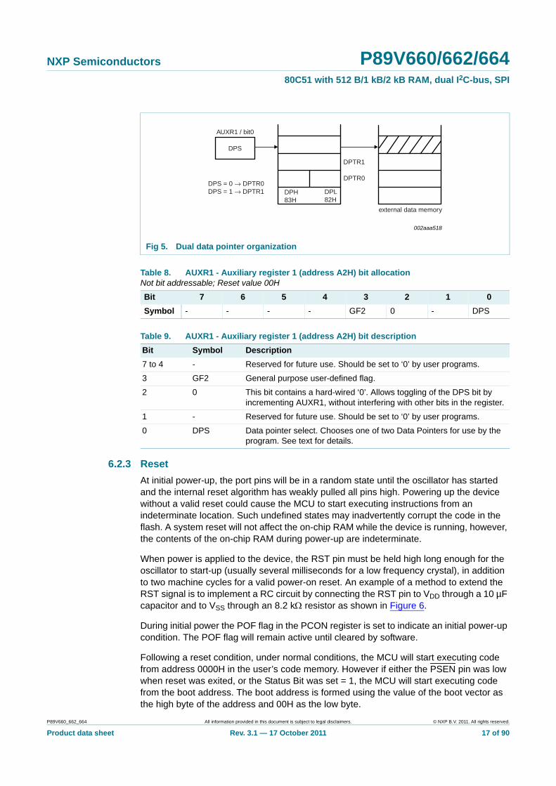
6.2.2 Dual data pointers
The device has two 16-bit data pointers. The DPTR Select (DPS) bit in AUXR1 determines which of the two data pointers is accessed. When DPS = 0, DPTR0 is selected; when DPS = 1, DPTR1 is selected. Quickly switching between the two data pointers can be accomplished by a single INC instruction on AUXR1 (see Figure 5).
Fig 4. Internal and external data memory structure
000H
2FFH
00H
FFH
UPPER 128 BINTERNAL RAM
LOWER 128 BINTERNAL RAM
(INDIRECT AND DIRECT
ADDRESSING)
(INDIRECTADDRESSING)
(DIRECTADDRESSING)
SPECIALFUNCTION
REGISTERS (SFRs)80H
FFH
FFFFH
000H
EXTERNALDATA
MEMORY
EXTERNALDATA
MEMORY
2FFH
0000H
EXTRAM = 0 EXTRAM = 1
EXPANDED RAM
0300H
(INDIRECTADDRESSING)
(INDIRECTADDRESSING)
(INDIRECTADDRESSING)
FFFFH
80H7FH
002aaa517
EXPANDEDRAM768 B
P89V660_662_664 All information provided in this document is subject to legal disclaimers. © NXP B.V. 2011. All rights reserved.
Product data sheet Rev. 3.1 — 17 October 2011 16 of 90
NXP Semiconductors P89V660/662/66480C51 with 512 B/1 kB/2 kB RAM, dual I2C-bus, SPI
6.2.3 Reset
At initial power-up, the port pins will be in a random state until the oscillator has started and the internal reset algorithm has weakly pulled all pins high. Powering up the device without a valid reset could cause the MCU to start executing instructions from an indeterminate location. Such undefined states may inadvertently corrupt the code in the flash. A system reset will not affect the on-chip RAM while the device is running, however, the contents of the on-chip RAM during power-up are indeterminate.
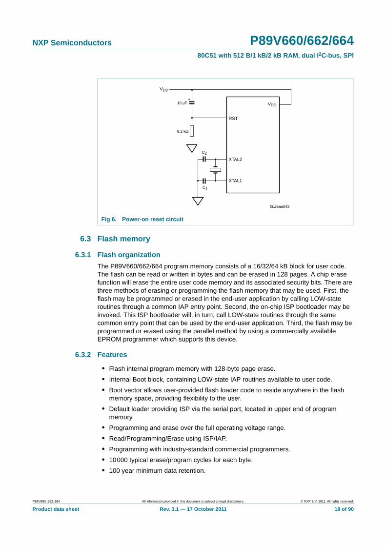
When power is applied to the device, the RST pin must be held high long enough for the oscillator to start-up (usually several milliseconds for a low frequency crystal), in addition to two machine cycles for a valid power-on reset. An example of a method to extend the RST signal is to implement a RC circuit by connecting the RST pin to VDD through a 10 µF capacitor and to VSS through an 8.2 k resistor as shown in Figure 6.
During initial power the POF flag in the PCON register is set to indicate an initial power-up condition. The POF flag will remain active until cleared by software.
Following a reset condition, under normal conditions, the MCU will start executing code from address 0000H in the user’s code memory. However if either the PSEN pin was low when reset was exited, or the Status Bit was set = 1, the MCU will start executing code from the boot address. The boot address is formed using the value of the boot vector as the high byte of the address and 00H as the low byte.
Fig 5. Dual data pointer organization
Table 8. AUXR1 - Auxiliary register 1 (address A2H) bit allocationNot bit addressable; Reset value 00H
Bit 7 6 5 4 3 2 1 0
Symbol - - - - GF2 0 - DPS
Table 9. AUXR1 - Auxiliary register 1 (address A2H) bit description
Bit Symbol Description
7 to 4 - Reserved for future use. Should be set to ‘0’ by user programs.
3 GF2 General purpose user-defined flag.
2 0 This bit contains a hard-wired ‘0’. Allows toggling of the DPS bit by incrementing AUXR1, without interfering with other bits in the register.
1 - Reserved for future use. Should be set to ‘0’ by user programs.
0 DPS Data pointer select. Chooses one of two Data Pointers for use by the program. See text for details.
DPL82H
DPS = 0 → DPTR0DPS = 1 → DPTR1
external data memory
DPS
002aaa518
DPH83H
DPTR0
DPTR1
AUXR1 / bit0
P89V660_662_664 All information provided in this document is subject to legal disclaimers. © NXP B.V. 2011. All rights reserved.
Product data sheet Rev. 3.1 — 17 October 2011 17 of 90
NXP Semiconductors P89V660/662/66480C51 with 512 B/1 kB/2 kB RAM, dual I2C-bus, SPI
6.3 Flash memory
6.3.1 Flash organization
The P89V660/662/664 program memory consists of a 16/32/64 kB block for user code. The flash can be read or written in bytes and can be erased in 128 pages. A chip erase function will erase the entire user code memory and its associated security bits. There are three methods of erasing or programming the flash memory that may be used. First, the flash may be programmed or erased in the end-user application by calling LOW-state routines through a common IAP entry point. Second, the on-chip ISP bootloader may be invoked. This ISP bootloader will, in turn, call LOW-state routines through the same common entry point that can be used by the end-user application. Third, the flash may be programmed or erased using the parallel method by using a commercially available EPROM programmer which supports this device.
6.3.2 Features
• Flash internal program memory with 128-byte page erase.
• Internal Boot block, containing LOW-state IAP routines available to user code.
• Boot vector allows user-provided flash loader code to reside anywhere in the flash memory space, providing flexibility to the user.
• Default loader providing ISP via the serial port, located in upper end of program memory.
• Programming and erase over the full operating voltage range.
• Read/Programming/Erase using ISP/IAP.
• Programming with industry-standard commercial programmers.
• 10000 typical erase/program cycles for each byte.
• 100 year minimum data retention.
Fig 6. Power-on reset circuit
002aaa543
VDD
VDD
8.2 kΩ
RST
XTAL2
XTAL1
C1
C2
10 μF
P89V660_662_664 All information provided in this document is subject to legal disclaimers. © NXP B.V. 2011. All rights reserved.
Product data sheet Rev. 3.1 — 17 October 2011 18 of 90
NXP Semiconductors P89V660/662/66480C51 with 512 B/1 kB/2 kB RAM, dual I2C-bus, SPI
6.3.3 Boot block
When the microcontroller programs its own flash memory, all of the low level details are handled by code (bootloader) that is contained in a Boot block. A user program calls the common entry point in the Boot block with appropriate parameters to accomplish the desired operation. Boot block operations include erase user code, program user code, program security bits, chip erase, etc. The Boot block logically overlays the program memory space from FC00H to FFFFH, when it is enabled. The Boot block may be disabled on-the-fly so that the upper 1 kB of user code is available to the user’s program.
6.3.4 Power-on reset code execution
The P89V660/662/664 contains two special flash elements: the Boot Vector and the Boot Status bit. Following reset, the P89V660/662/664 examines the contents of the Boot Status bit. If the Boot Status bit is set to zero, power-up execution starts at location 0000H, which is the normal start address of the user’s application code. When the Boot Status bit is set to a value other than zero, the contents of the Boot Vector are used as the high byte of the execution address and the low byte is set to 00H
Table 10 shows the factory default Boot Vector setting for this device. A factory-provided bootloader is pre-programmed into the address space indicated and uses the indicated boot loader entry point to perform ISP functions.
6.3.5 Hardware activation of the bootloader
The bootloader can also be executed by forcing the device into ISP mode during a power-on sequence. This has the same effect as having a non-zero status byte. This allows an application to be built that will normally execute user code but can be manually forced into ISP operation. If the factory default setting for the boot vector (FCH) is changed, it will no longer point to the factory pre-programmed ISP bootloader code. After programming the flash, the status byte should be programmed to zero in order to allow execution of the user’s application code beginning at address 0000H.
6.3.6 ISP
ISP is performed without removing the microcontroller from the system. The ISP facility consists of a series of internal hardware resources coupled with internal firmware to facilitate remote programming of the P89V660/662/664 through the serial port. This firmware is provided by NXP and embedded within each P89V660/662/664 device. The NXP ISP facility has made in-circuit programming in an embedded application possible with a minimum of additional expense in components and circuit board area. The ISP function uses five pins (VDD, VSS, TXD, RXD, and RST). Only a small connector needs to be available to interface your application to an external circuit in order to use this feature.
6.3.7 Using ISP
The ISP feature allows for a wide range of baud rates to be used in your application, independent of the oscillator frequency. It is also adaptable to a wide range of oscillator frequencies. This is accomplished by measuring the bit-time of a single bit in a received character. This information is then used to program the baud rate in terms of timer counts
Table 10. Default boot vector values and ISP entry points
Device Default boot vector Default bootloader entry point
Default bootloader code range
P89V660/662/664 FCH FC00H FC00H to FFFFH
P89V660_662_664 All information provided in this document is subject to legal disclaimers. © NXP B.V. 2011. All rights reserved.
Product data sheet Rev. 3.1 — 17 October 2011 19 of 90
NXP Semiconductors P89V660/662/66480C51 with 512 B/1 kB/2 kB RAM, dual I2C-bus, SPI
based on the oscillator frequency. The ISP feature requires that an initial character (an uppercase U) be sent to the P89V660/662/664 to establish the baud rate. The ISP firmware provides auto-echo of received characters. Once baud rate initialization has been performed, the ISP firmware will only accept Intel Hex-type records. Intel Hex records consist of ASCII characters used to represent hexadecimal values and are summarized below:
:NNAAAARRDD..DDCC<crlf>
In the Intel Hex record, the ‘NN’ represents the number of data bytes in the record. The P89V660/662/664 will accept up to 32 data bytes. The ‘AAAA’ string represents the address of the first byte in the record. If there are zero bytes in the record, this field is often set to 0000. The ‘RR’ string indicates the record type. A record type of ‘00’ is a data record. A record type of ‘01’ indicates the end-of-file mark. In this application, additional record types will be added to indicate either commands or data for the ISP facility.
The maximum number of data bytes in a record is limited to 32 (decimal). ISP commands are summarized in Table 11. As a record is received by the P89V660/662/664, the information in the record is stored internally and a checksum calculation is performed. The operation indicated by the record type is not performed until the entire record has been received. Should an error occur in the checksum, the P89V660/662/664 will send an ‘X’ out the serial port indicating a checksum error. If the checksum calculation is found to match the checksum in the record, then the command will be executed. In most cases, successful reception of the record will be indicated by transmitting a ‘.’ character out the serial port.
Table 11. ISP hex record formats
Record type Command/data function
00 Program User Code Memory
:nnaaaa00dd..ddcc
Where:
nn = number of bytes to program
aaaa = address
dd..dd = data bytes
cc = checksum
Example:
:09000000010203040506070809CA
01 End of File (EOF), no operation
:xxxxxx01cc
Where:
xxxxxx = required field but value is a ‘don’t care’
cc = checksum
Example:
:00000001FF
02 not used
P89V660_662_664 All information provided in this document is subject to legal disclaimers. © NXP B.V. 2011. All rights reserved.
Product data sheet Rev. 3.1 — 17 October 2011 20 of 90
NXP Semiconductors P89V660/662/66480C51 with 512 B/1 kB/2 kB RAM, dual I2C-bus, SPI
03 Miscellaneous Write Functions
:nnxxxx03ffssddcc
Where:
nn = number of bytes in the record
xxxx = required field but value is a ‘don’t care’
ff = subfunction code
ss = selection code
dd = data (if needed)
cc = checksum
Subfunction code = 01 (Erase Blocks)
ff = 01
ss = block code, as shown below
block 0, 0k to 8k, 00H
block 1, 8k to 16k, 20H
block 0, 16k to 32k, 40H
block 0, 32k to 48k, 80H
block 0, 48k to 64k, C0H
Subfunction code = 04 (Erase Boot vector and Status Bit)
ff = 04
ss = don’t care
Subfunction code = 05 (Program security bits)
ff = 05
ss = 00 program security bit 1
ss = 01 program security bit 2
ss = 02 program security bit 3
Subfunction code = 06 (Program Status bit, Boot vector, 6x/12x bit)
ff = 06
dd = data (for Boot vector)
ss = 00 program Status bit
ss = 01 program Boot vector
ss = 02 program 6x/12x bit
Subfunction code = 07 (Chip Erase)
Erases code memory and security bits, programs default Boot vector and Status bit
ff = 07
Subfunction code = 08 (Erase page, 128 B)
ff = 08
ss = high byte of page address (A[15:8])
dd = low byte of page address (A[7:0])
Example:
:0300000308E000F2 (erase page at E000H)
Table 11. ISP hex record formats …continued
Record type Command/data function
P89V660_662_664 All information provided in this document is subject to legal disclaimers. © NXP B.V. 2011. All rights reserved.
Product data sheet Rev. 3.1 — 17 October 2011 21 of 90
NXP Semiconductors P89V660/662/66480C51 with 512 B/1 kB/2 kB RAM, dual I2C-bus, SPI
04 Display Device Data or Blank Check
:05xxxx04sssseeeeffcc
Where
05 = number of bytes in the record
xxxx = required field but value is a ‘don’t care’
04 = function code for display or blank check
ssss = starting address, MSB first
eeee = ending address, MSB first
ff = subfunction
00 = display data
01 = blank check
cc = checksum
Subfunction codes:
Example:
:0500000400001FFF00D9 (display from 0000H to 1FFFH)
05 Miscellaneous Read Functions
:02xxxx05ffsscc
Where:
02 = number of bytes in the record
xxxx = required field but value is a ‘don’t care’
05 = function code for misc read
ffss = subfunction and selection code
0000 = read manufacturer id
0001 = read device id 1
0002 = read device id 2
0003 = read 6x/12x bit (bit 7 = 1 is 6x, bit 7 = 0 is 12x)
0080 = read boot code version
0700 = read security bits
0701 = read Status bit
0702 = read Boot vector
cc = checksum
Example:
:020000050000F9 (display manufacturer id)
06 Direct Load of Baud Rate
:02xxxx06HHLLcc
Where:
02 = number of bytes in the record
xxxx = required field but value is a ‘don’t care’
HH = high byte of timer T2
LL = low byte of timer T2
cc = checksum
Example:
:02000006FFFFcc (load T2 = FFFF)
Table 11. ISP hex record formats …continued
Record type Command/data function
P89V660_662_664 All information provided in this document is subject to legal disclaimers. © NXP B.V. 2011. All rights reserved.
Product data sheet Rev. 3.1 — 17 October 2011 22 of 90
NXP Semiconductors P89V660/662/66480C51 with 512 B/1 kB/2 kB RAM, dual I2C-bus, SPI
6.3.8 IAP method
Several IAP calls are available for use by an application program to permit selective erasing, reading and programming of flash pages, security bits, security bits, Status bit, and device id. All calls are made through a common interface, PGM_MTP. The programming functions are selected by setting up the microcontroller’s registers before making a call to PGM_MTP at FFF0H. The IAP calls are shown in Table 12.
Table 12. IAP function calls
IAP function IAP call parameters
Read Id Input parameters:
R1 = 00H or 80H (WDT feed)
DPH = 00H
DPL = 00H = manufacturer id
DPL = 01H = device id 1
DPL = 02H = device id 2
DPL = 03H = 6x/12x bit (bit 7 = 1 = 6x)
DPL = 80H = ISP version number
Return parameter(s):
ACC = requested parameter
Erase 8 kB/16 kB code block Input parameters:
R1 = 01H or 81H (WDT feed)
DPL = 00H, block 0, 0 kB to 8 kB
DPL = 20H, block 1, 8 kB to 16 kB
DPL = 40H, block 2, 16 kB to 32 kB
DPL = 80H, block 3, 32 kB to 48 kB
DPL = C0H, block 4, 48 kB to 64 kB
Return parameter(s):
ACC = 00 = pass
ACC = !00 = fail
Program User Code Input parameters:
R1 = 02H or 82H (WDT feed)
DPH = memory address MSB
DPL = memory address LSB
ACC = byte to program
Return parameter(s):
ACC = 00 = pass
ACC = !00 = fail
Read User Code Input parameters:
R1 = 03H or 83H (WDT feed)
DPH = memory address MSB
DPL = memory address LSB
Return parameter(s):
ACC = device data
P89V660_662_664 All information provided in this document is subject to legal disclaimers. © NXP B.V. 2011. All rights reserved.
Product data sheet Rev. 3.1 — 17 October 2011 23 of 90
NXP Semiconductors P89V660/662/66480C51 with 512 B/1 kB/2 kB RAM, dual I2C-bus, SPI
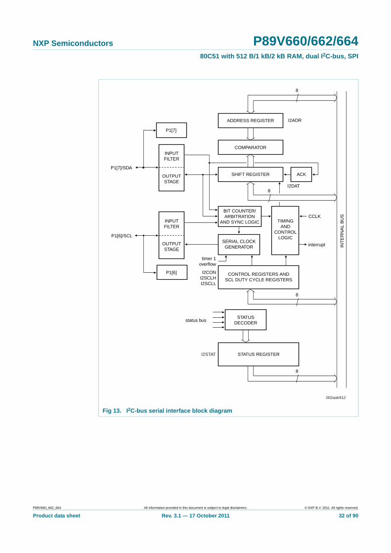
6.4 I2C-bus interface
The I2C-bus uses two wires, Serial Clock (SCL) and Serial Data (SDA) to transfer information between devices connected to the bus, and has the following features:
• Bidirectional data transfer between masters and slaves
Erase Status bit and Boot vector Input parameters:
R1 = 04H or 84H (WDT feed)
DPL = don’t care
DPH = don’t care
Return parameter(s):
ACC = 00 = pass
ACC = !00 = fail
Program Security bits Input parameters:
R1 = 05H or 85H (WDT feed)
DPL = 00H = security bit 1
DPL = 01H = security bit 2
DPL = 02H = security bit 3
Return parameter(s):
ACC = 00 = pass
ACC = !00 = fail
Program Status bit, Boot vector, 6x/12x bit
Input parameters:
R1 = 06H or 86H (WDT feed)
DPL = 00H = program Status bit
DPL = 01H = program Boot vector
DPL = 02H = 6x/12x bit
ACC = Boot vector value to program
Return parameter(s):
ACC = 00 = pass
ACC = !00 = fail
Read Security bits, Status bit, Boot vector
Input parameters:
ACC = 07H or 87H (WDT feed)
DPL = 00H = security bits
DPL = 01H = Status bit
DPL = 02H = Boot vector
Return parameter(s):
ACC = 00 SoftICE S/N-match 0 SB 0 DBL_CLK
Erase page Input parameters:
R1 = 08H or 88H (WDT feed)
DPH = page address high byte
DPL = page address low byte
Return parameter(s):
ACC = 00 = pass
ACC = !00 = fail
Table 12. IAP function calls …continued
IAP function IAP call parameters
P89V660_662_664 All information provided in this document is subject to legal disclaimers. © NXP B.V. 2011. All rights reserved.
Product data sheet Rev. 3.1 — 17 October 2011 24 of 90
NXP Semiconductors P89V660/662/66480C51 with 512 B/1 kB/2 kB RAM, dual I2C-bus, SPI
• Multimaster bus (no central master)
• Arbitration between simultaneously transmitting masters without corruption of serial data on the bus
• Serial clock synchronization allows devices with different bit rates to communicate via one serial bus
• Serial clock synchronization can be used as a handshake mechanism to suspend and resume serial transfer
• The I2C-bus may be used for test and diagnostic purposes
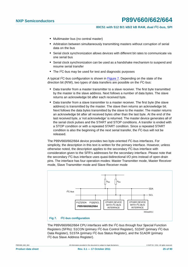
A typical I2C-bus configuration is shown in Figure 7. Depending on the state of the direction bit (R/W), two types of data transfers are possible on the I2C-bus:
• Data transfer from a master transmitter to a slave receiver. The first byte transmitted by the master is the slave address. Next follows a number of data bytes. The slave returns an acknowledge bit after each received byte.
• Data transfer from a slave transmitter to a master receiver. The first byte (the slave address) is transmitted by the master. The slave then returns an acknowledge bit. Next follows the data bytes transmitted by the slave to the master. The master returns an acknowledge bit after all received bytes other than the last byte. At the end of the last received byte, a ‘not acknowledge’ is returned. The master device generates all of the serial clock pulses and the START and STOP conditions. A transfer is ended with a STOP condition or with a repeated START condition. Since a repeated START condition is also the beginning of the next serial transfer, the I2C-bus will not be released.
The P89V660/662/664 device provides two byte-oriented I2C-bus interfaces. For simplicity, the description in this text is written for the primary interface. However, unless otherwise noted, the description applies to the secondary I2C-bus interface with consideration given to the SFR’s addresses for the secondary interface. Please note that the secondary I2C-bus interface uses quasi-bidirectional I/O pins instead of open-drain pins. The interface has four operation modes: Master Transmitter mode, Master Receiver mode, Slave Transmitter mode and Slave Receiver mode
The P89V660/662/664 CPU interfaces with the I2C-bus through four Special Function Registers (SFRs): S1CON (primary I2C-bus Control Register), S1DAT (primary I2C-bus Data Register), S1STA (primary I2C-bus Status Register), and the S1ADR (primary I2C-bus Slave Address Register).
Fig 7. I2C-bus configuration
OTHER DEVICEWITH I2C-BUS
INTERFACE
SDA
SCL
RpuRpu
OTHER DEVICEWITH I2C-BUS
INTERFACE
P1[7]/SDA P1[6]/SCL
P89V660/662/664
I2C-bus
002aab911
P89V660_662_664 All information provided in this document is subject to legal disclaimers. © NXP B.V. 2011. All rights reserved.
Product data sheet Rev. 3.1 — 17 October 2011 25 of 90
NXP Semiconductors P89V660/662/66480C51 with 512 B/1 kB/2 kB RAM, dual I2C-bus, SPI
6.4.1 I2C-bus data register
S1DAT register contains the data to be transmitted or the data received. The CPU can read and write to this 8-bit register while it is not in the process of shifting a byte. Thus this register should only be accessed when the SI bit is set. Data in S1DAT remains stable as long as the SI bit is set. Data in S1DAT is always shifted from right to left: the first bit to be transmitted is the MSB (bit 7), and after a byte has been received, the first bit of received data is located at the MSB of S1DAT.
6.4.2 I2C-bus slave address register
The S1ADR register is readable and writable, and is only used when the I2C-bus interface is set to slave mode. In master mode, this register has no effect. The LSB of S1ADR is general call bit. When this bit is set, the general call address (00H) is recognized.
6.4.3 I2C-bus control register
The CPU can read and write this register. There are two bits are affected by hardware: the SI bit and the STO bit. The SI bit is set by hardware and the STO bit is cleared by hardware.
CR2:0 determines the SCL source and frequency when the I2C-bus is in master mode. In slave mode these bits are ignored and the bus will automatically synchronize with any clock frequency up to 100 kHz from the master I2C-bus device. Timer 1 should be programmed by the user in 8 bit auto-reload mode (Mode 2) when used as the SCL source. See Table 17.
The STA bit is START flag. Setting this bit causes the I2C-bus interface to enter master mode and attempt transmitting a START condition or transmitting a repeated START condition when it is already in master mode.
The STO bit is STOP flag. Setting this bit causes the I2C-bus interface to transmit a STOP condition in master mode, or recovering from an error condition in slave mode.
If the STA and STO are both set, then a STOP condition is transmitted to the I2C-bus if it is in master mode, and transmits a START condition afterwards. If it is in slave mode, an internal STOP condition will be generated, but it is not transmitted to the bus.
Table 13. I2C-bus slave address register (S1ADR - address DBH) bit allocation
Bit 7 6 5 4 3 2 1 0
Symbol S1ADR.6 S1ADR.5 S1ADR.4 S1ADR.3 S1ADR.2 S1ADR.1 S1ADR.0 S1GC
Reset 0 0 0 0 0 0 0 0
Table 14. I2C-bus slave address register (S1ADR - address DBH) bit description
Bit Symbol Description
7:1 S1ADR7:1 7 bit own slave address. When in master mode, the contents of this register has no effect.
0 S1GC General call bit. When set, the general call address (00H) is recognized, otherwise it is ignored.
P89V660_662_664 All information provided in this document is subject to legal disclaimers. © NXP B.V. 2011. All rights reserved.
Product data sheet Rev. 3.1 — 17 October 2011 26 of 90
NXP Semiconductors P89V660/662/66480C51 with 512 B/1 kB/2 kB RAM, dual I2C-bus, SPI
Table 15. I2C-bus control register (S1CON - address D8H) bit allocation
Bit 7 6 5 4 3 2 1 0
Symbol CR2 ENS1 STA STO SI AA CR1 CR0
Reset x 0 0 0 0 0 x 0
Table 16. I2C-bus control register (S1CON - address D8H) bit description
Bit Symbol Description
7,1,0 CR2:0 SCL clock selection. See Table 17.
2 AA The Assert Acknowledge Flag. When set to 1, an acknowledge (LOW-state to SDA) will be returned during the acknowledge clock pulse on the SCL line on the following situations:
1. The ‘own slave address’ has been received.
2. The general call address has been received while the general call bit (GC) in S1ADR is set.
3. A data byte has been received while the I2C-bus interface is in the Master Receiver mode.
4. A data byte has been received while the I2C-bus interface is in the addressed Slave Receiver mode.
When cleared to 0, an not acknowledge (HIGH-state to SDA) will be returned during the acknowledge clock pulse on the SCL line on the following situations:
1. A data byte has been received while the I2C-bus interface is in the Master Receiver mode.
2. A data byte has been received while the I2C-bus interface is in the addressed Slave Receiver mode.
3 SI I2C-bus Interrupt Flag. This bit is set when one of the 25 possible I2C-bus states is entered. When EA bit and EI2C (IEN1.0) bit are both set, an interrupt is requested when SI is set. Must be cleared by software by writing 0 to this bit.
4 STO STOP Flag. STO = 1: In master mode, a STOP condition is transmitted to the I2C-bus. When the bus detects the STOP condition, it will clear STO bit automatically. In slave mode, setting this bit can recover from an error condition. In this case, no STOP condition is transmitted to the bus. The hardware behaves as if a STOP condition has been received and it switches to ‘not addressed’ Slave Receiver mode. The STO flag is cleared by hardware automatically.
5 STA Start Flag. STA = 1: I2C-bus enters master mode, checks the bus and generates a START condition if the bus is free. If the bus is not free, it waits for a STOP condition (which will free the bus) and generates a START condition after a delay of a half clock period of the internal clock generator. When the I2C-bus interface is already in master mode and some data is transmitted or received, it transmits a repeated START condition. STA may be set at any time, it may also be set when the I2C-bus interface is in an addressed slave mode. STA = 0: no START condition or repeated START condition will be generated.
6 ENS1 I2C-bus Interface Enable. When set, enables the I2C-bus interface. When clear, the I2C-bus function is disabled.
Table 17. I2C-bus clock rates
CR2:0 Bit frequency at fosc
6-clock mode 12-clock mode fosc divided by
6 MHz 12 MHZ 6 MHz 12 MHz 6X 12X
000 47 94 23 47 128 256
001 54 107 27 54 112 224
010 63 125 31 63 96 192
011 75 150 37 75 80 160
100 12.5 25 6.25 12.5 480 960
P89V660_662_664 All information provided in this document is subject to legal disclaimers. © NXP B.V. 2011. All rights reserved.
Product data sheet Rev. 3.1 — 17 October 2011 27 of 90
NXP Semiconductors P89V660/662/66480C51 with 512 B/1 kB/2 kB RAM, dual I2C-bus, SPI
6.4.4 I2C-bus status register
This is a read-only register. It contains the status code of the I2C-bus interface. The least three bits are always 0. There are 26 possible status codes. When the code is F8H, there is no relevant information available and SI bit is not set. All other 25 status codes correspond to defined I2C-bus states. When any of these states entered, the SI bit will be set. Refer to Table 22 to Table 25 for details.
6.4.5 I2C-bus operation modes
6.4.5.1 Master transmitter mode
In this mode data is transmitted from master to slave. Before the Master Transmitter mode can be entered, S1CON must be initialized as follows:
CR2:0 define the bit rate (See Table 17). ENS1 must be set to 1 to enable the I2C-bus function. If the AA bit is 0, it will not acknowledge its own slave address or the general call address in the event of another device becoming master of the bus and it can not enter slave mode. STA, STO, and SI bits must be cleared to 0.
The first byte transmitted contains the slave address of the receiving device (7 bits) and the data direction bit. In this case, the data direction bit (R/W) will be logic 0 indicating a write. Data is transmitted 8 bits at a time. After each byte is transmitted, an acknowledge bit is received. START and STOP conditions are output to indicate the beginning and the end of a serial transfer.
101 100 200 50 100 60 120
110 200 400 100 200 30 60
111 0.49 < 62.5 0.98 < 50.0 0.24 < 62.5 0.49 < 62.5 48 x (Timer 1 reload)
96 x (Timer 1 reload)
Table 17. I2C-bus clock rates …continued
CR2:0 Bit frequency at fosc
6-clock mode 12-clock mode fosc divided by
6 MHz 12 MHZ 6 MHz 12 MHz 6X 12X
Table 18. I2C-bus status register (S1STA - address D9H) bit allocation
Bit 7 6 5 4 3 2 1 0
Symbol SC.4 SC.3 SC.2 SC.1 SC.0 0 0 0
Reset 0 0 0 0 0 0 0 0
Table 19. I2C-bus status register (S1STA - address D9H) bit description
Bit Symbol Description
7:3 SC[4:0] I2C-bus Status code.
2:0 - Reserved, are always set to 0.
Table 20. I2C-bus control register (S1CON - address D8H)
Bit 7 6 5 4 3 2 1 0
Symbol CR2 ENS1 STA STO SI AA CR1 CR0
Value bit rate 1 0 0 0 x bit rate bit rate
P89V660_662_664 All information provided in this document is subject to legal disclaimers. © NXP B.V. 2011. All rights reserved.
Product data sheet Rev. 3.1 — 17 October 2011 28 of 90
NXP Semiconductors P89V660/662/66480C51 with 512 B/1 kB/2 kB RAM, dual I2C-bus, SPI
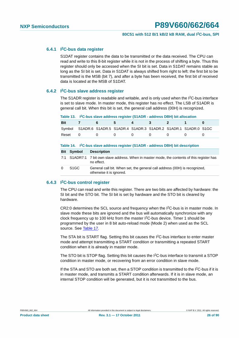
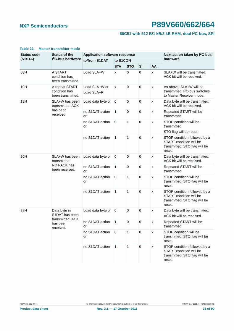
The I2C-bus will enter Master Transmitter mode by setting the STA bit. The I2C-bus logic will send the START condition as soon as the bus is free. After the START condition is transmitted, the SI bit is set, and the status code in S1STA should be 08H. This status code must be used to vector to an interrupt service routine where the user should load the slave address to S1DAT and data direction bit (SLA+W). The SI bit must be cleared before the data transfer can continue.
When the slave address and R/W bit have been transmitted and an acknowledgment bit has been received, the SI bit is set again, and the possible status codes are 18H, 20H, or 38H for the master mode or 68H, 78H, or 0B0H if the slave mode was enabled (setting AA = Logic 1). The appropriate action to be taken for each of these status codes is shown in Table 22.
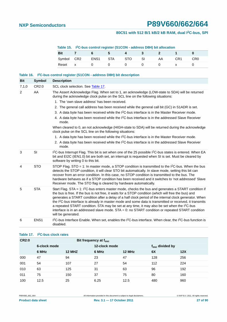
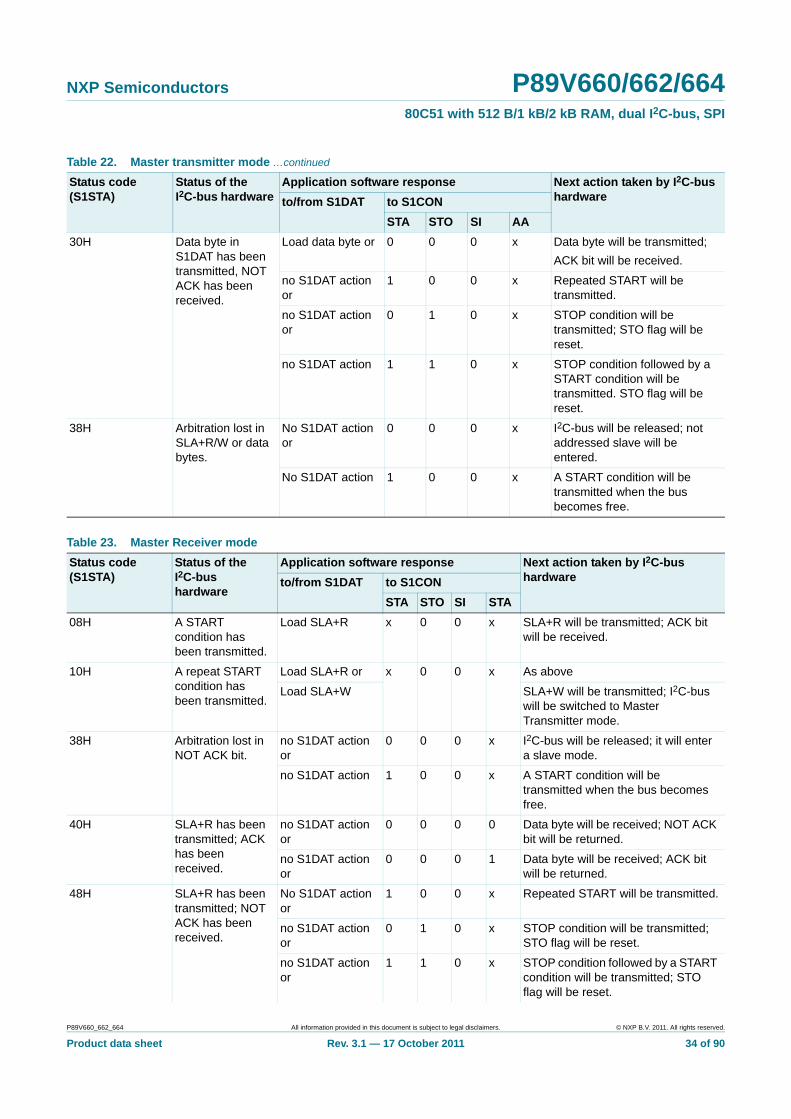
6.4.5.2 Master receiver mode
In the Master Receiver mode, data is received from a slave transmitter. The transfer started in the same manner as in the Master Transmitter mode. When the START condition has been transmitted, the interrupt service routine must load the slave address and the data direction bit to I2C-bus Data Register (S1DAT). The SI bit must be cleared before the data transfer can continue.
When the slave address and data direction bit have been transmitted and an acknowledge bit has been received, the SI bit is set, and the Status Register will show the status code. For master mode, the possible status codes are 40H, 48H, or 38H. For slave mode, the possible status codes are 68H, 78H, or B0H. Refer to Table 24 for details.
After a repeated START condition, I2C-bus may switch to the Master Transmitter mode.
Fig 8. Format in the Master Transmitter mode
S R/W A DATA DATA
data transferred(n Bytes + acknowledge)
A A/A Pslave address
logic 0 = writelogic 1 = read
from master to slave
from slave to master
A = acknowledge (SDA LOW)A = not acknowledge (SDA HIGH)S = START conditionP = STOP condition
002aaa929
Fig 9. Format of Master Receiver mode
S R Aslave address
logic 0 = writelogic 1 = read
from master to slave
from slave to master
A = acknowledge (SDA LOW)A = not acknowledge (SDA HIGH)S = START condition
002aaa930
DATA DATA
data transferred(n Bytes + acknowledge)
A A P
P89V660_662_664 All information provided in this document is subject to legal disclaimers. © NXP B.V. 2011. All rights reserved.
Product data sheet Rev. 3.1 — 17 October 2011 29 of 90
NXP Semiconductors P89V660/662/66480C51 with 512 B/1 kB/2 kB RAM, dual I2C-bus, SPI
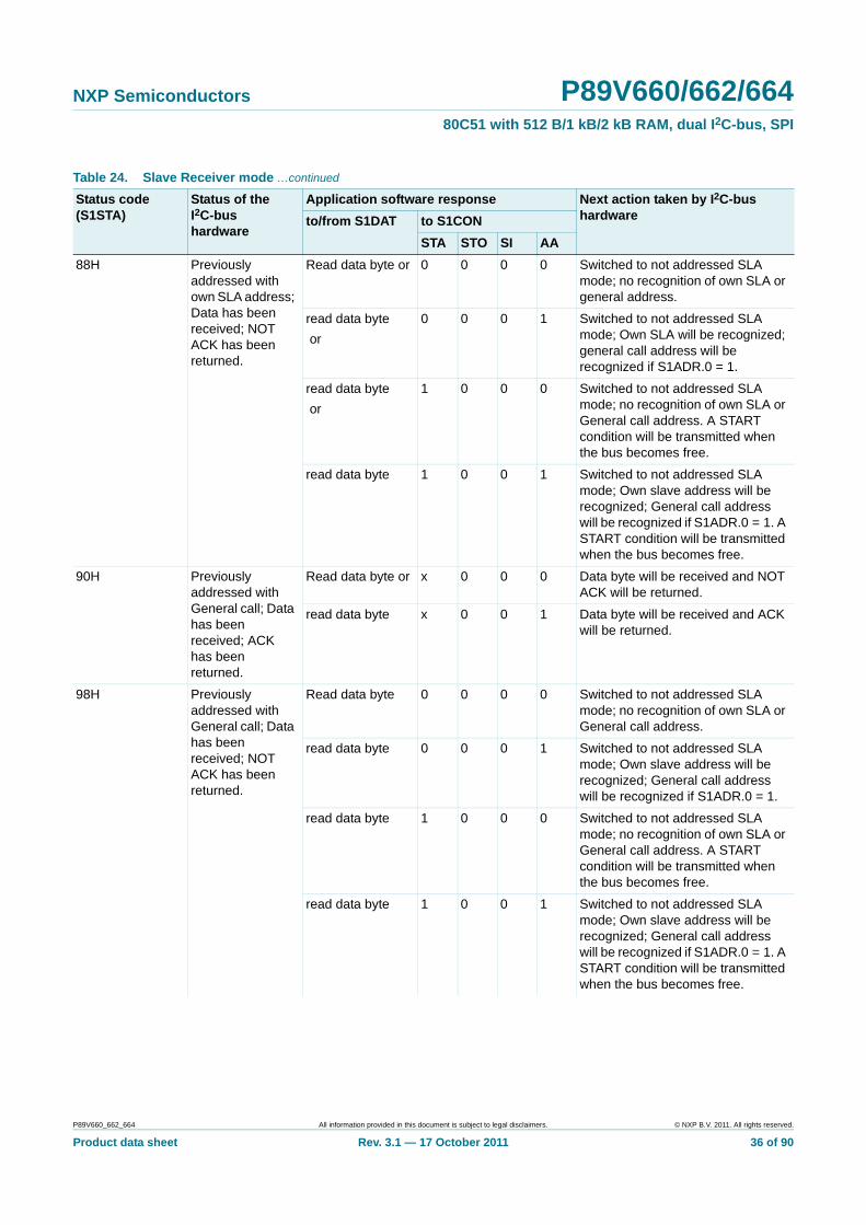
6.4.5.3 Slave receiver mode
In the Slave Receiver mode, data bytes are received from a master transmitter. To initialize the Slave Receiver mode, the user should write the slave address to the Slave Address Register (S1ADR) and the I2C-bus Control Register (S1CON) should be configured as follows:
CR2:0 are not used for slave mode. ENS1 must be set = 1 to enable I2C-bus function. AA bit must be set = 1 to acknowledge its own slave address or the general call address. STA, STO and SI are cleared to 0.
After S1ADR and S1CON are initialized, the interface waits until it is addressed by its own address or general address followed by the data direction bit which is 0(W). If the direction bit is 1(R), it will enter Slave Transmitter mode. After the address and the direction bit have been received, the SI bit is set and a valid status code can be read from the Status Register(S1STA). Refer to Table 25 for the status codes and actions.
6.4.5.4 Slave transmitter mode
The first byte is received and handled as in the Slave Receiver mode. However, in this mode, the direction bit will indicate that the transfer direction is reversed. Serial data is transmitted via P1[7]/SDA while the serial clock is input through P1[6]/SCL. START and
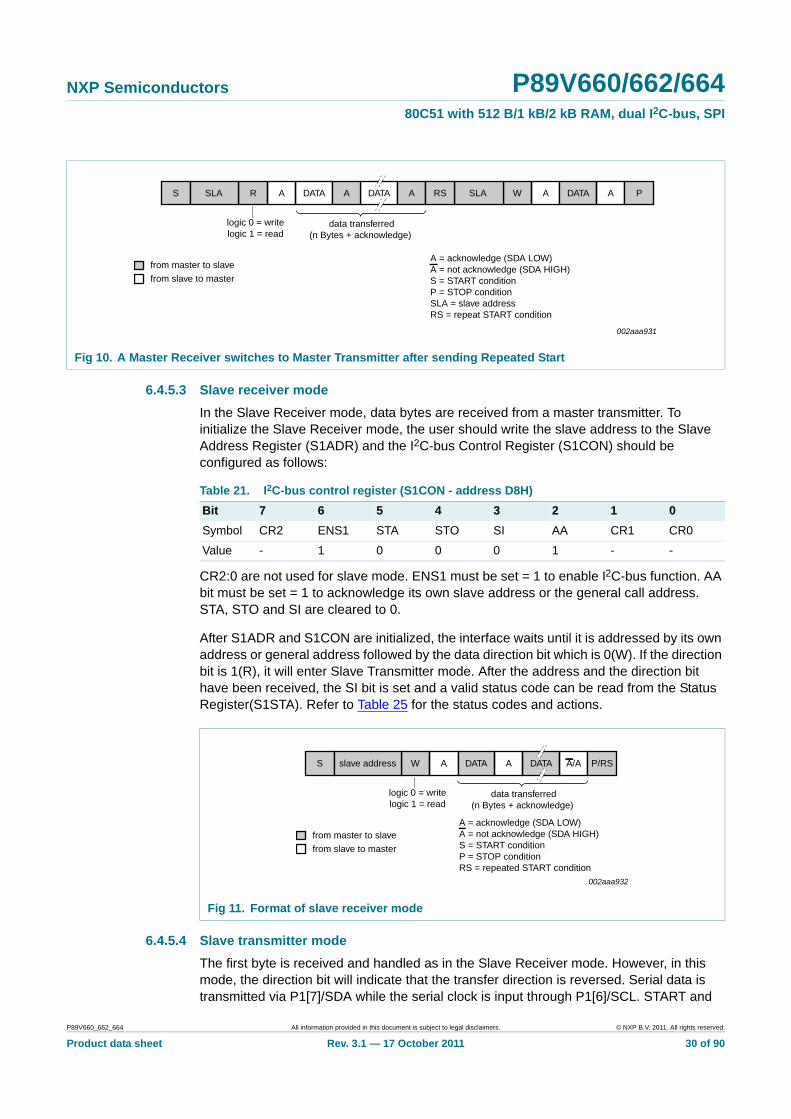
Fig 10. A Master Receiver switches to Master Transmitter after sending Repeated Start
S R ASLA
logic 0 = writelogic 1 = read
from master to slave
from slave to master
002aaa931
DATA DATA
data transferred(n Bytes + acknowledge)
A W ASLA DATA A PA RS
A = acknowledge (SDA LOW)A = not acknowledge (SDA HIGH)S = START conditionP = STOP conditionSLA = slave addressRS = repeat START condition
Table 21. I2C-bus control register (S1CON - address D8H)
Bit 7 6 5 4 3 2 1 0
Symbol CR2 ENS1 STA STO SI AA CR1 CR0
Value - 1 0 0 0 1 - -
Fig 11. Format of slave receiver mode
S W Aslave address
logic 0 = writelogic 1 = read
from master to slave
from slave to master
A = acknowledge (SDA LOW)A = not acknowledge (SDA HIGH)S = START conditionP = STOP conditionRS = repeated START condition
002aaa932
DATA DATA
data transferred(n Bytes + acknowledge)
A A/A P/RS
P89V660_662_664 All information provided in this document is subject to legal disclaimers. © NXP B.V. 2011. All rights reserved.
Product data sheet Rev. 3.1 — 17 October 2011 30 of 90

NXP Semiconductors P89V660/662/66480C51 with 512 B/1 kB/2 kB RAM, dual I2C-bus, SPI
STOP conditions are recognized as the beginning and end of a serial transfer. In a given application, the I2C-bus may operate as a master and as a slave. In the slave mode, the I2C-bus hardware looks for its own slave address and the general call address. If one of these addresses is detected, an interrupt is requested. When the microcontrollers wishes to become the bus master, the hardware waits until the bus is free before the master mode is entered so that a possible slave action is not interrupted. If bus arbitration is lost in the master mode, the I2C-bus switches to the slave mode immediately and can detect its own slave address in the same serial transfer.
Fig 12. Format of slave transmitter mode
S R Aslave address
logic 0 = writelogic 1 = read
from master to slave
from slave to master
A = acknowledge (SDA LOW)A = not acknowledge (SDA HIGH)S = START conditionP = STOP condition
002aaa933
DATA DATA
data transferred(n Bytes + acknowledge)
A A P
P89V660_662_664 All information provided in this document is subject to legal disclaimers. © NXP B.V. 2011. All rights reserved.
Product data sheet Rev. 3.1 — 17 October 2011 31 of 90
NXP Semiconductors P89V660/662/66480C51 with 512 B/1 kB/2 kB RAM, dual I2C-bus, SPI
Fig 13. I2C-bus serial interface block diagram
INT
ER
NA
L B
US
002aab912
ADDRESS REGISTER
COMPARATOR
SHIFT REGISTER
8
I2ADR
ACK
BIT COUNTER/ARBITRATION
AND SYNC LOGIC
8I2DAT
TIMINGAND
CONTROLLOGIC
SERIAL CLOCKGENERATOR
CCLK
interrupt
INPUTFILTER
OUTPUTSTAGE
INPUTFILTER
OUTPUTSTAGE
P1[7]
P1[7]/SDA
P1[6]/SCL
P1[6]
timer 1overflow
CONTROL REGISTERS ANDSCL DUTY CYCLE REGISTERS
I2CONI2SCLHI2SCLL
8
STATUSDECODERstatus bus
STATUS REGISTER
8
I2STAT
P89V660_662_664 All information provided in this document is subject to legal disclaimers. © NXP B.V. 2011. All rights reserved.
Product data sheet Rev. 3.1 — 17 October 2011 32 of 90
NXP Semiconductors P89V660/662/66480C51 with 512 B/1 kB/2 kB RAM, dual I2C-bus, SPI
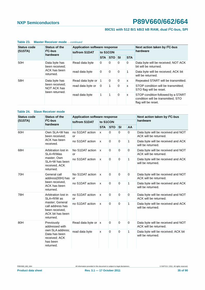
Table 22. Master transmitter mode
Status code (S1STA)
Status of the I2C-bus hardware
Application software response Next action taken by I2C-bus hardwareto/from S1DAT to S1CON
STA STO SI AA
08H A START condition has been transmitted.
Load SLA+W x 0 0 x SLA+W will be transmitted; ACK bit will be received.
10H A repeat START condition has been transmitted.
Load SLA+W or
Load SLA+R
x 0 0 x As above; SLA+W will be transmitted; I2C-bus switches to Master Receiver mode.
18H SLA+W has been transmitted; ACK has been received.
Load data byte or 0 0 0 x Data byte will be transmitted; ACK bit will be received.
no S1DAT action or
1 0 0 x Repeated START will be transmitted.
no S1DAT action or
0 1 0 x STOP condition will be transmitted;
STO flag will be reset.
no S1DAT action 1 1 0 x STOP condition followed by a START condition will be transmitted; STO flag will be reset.
20H SLA+W has been transmitted; NOT-ACK has been received.
Load data byte or 0 0 0 x Data byte will be transmitted; ACK bit will be received.
no S1DAT action or
1 0 0 x Repeated START will be transmitted.
no S1DAT action or
0 1 0 x STOP condition will be transmitted; STO flag will be reset.
no S1DAT action 1 1 0 x STOP condition followed by a START condition will be transmitted; STO flag will be reset.
28H Data byte in S1DAT has been transmitted; ACK has been received.
Load data byte or 0 0 0 x Data byte will be transmitted;
ACK bit will be received.
no S1DAT action or
1 0 0 x Repeated START will be transmitted.
no S1DAT action or
0 1 0 x STOP condition will be transmitted; STO flag will be reset.
no S1DAT action 1 1 0 x STOP condition followed by a START condition will be transmitted; STO flag will be reset.
P89V660_662_664 All information provided in this document is subject to legal disclaimers. © NXP B.V. 2011. All rights reserved.
Product data sheet Rev. 3.1 — 17 October 2011 33 of 90
NXP Semiconductors P89V660/662/66480C51 with 512 B/1 kB/2 kB RAM, dual I2C-bus, SPI
30H Data byte in S1DAT has been transmitted, NOT ACK has been received.
Load data byte or 0 0 0 x Data byte will be transmitted;
ACK bit will be received.
no S1DAT action or
1 0 0 x Repeated START will be transmitted.
no S1DAT action or
0 1 0 x STOP condition will be transmitted; STO flag will be reset.
no S1DAT action 1 1 0 x STOP condition followed by a START condition will be transmitted. STO flag will be reset.
38H Arbitration lost in SLA+R/W or data bytes.
No S1DAT action or
0 0 0 x I2C-bus will be released; not addressed slave will be entered.
No S1DAT action 1 0 0 x A START condition will be transmitted when the bus becomes free.
Table 22. Master transmitter mode …continued
Status code (S1STA)
Status of the I2C-bus hardware
Application software response Next action taken by I2C-bus hardwareto/from S1DAT to S1CON
STA STO SI AA
Table 23. Master Receiver mode
Status code (S1STA)
Status of the I2C-bus hardware
Application software response Next action taken by I2C-bus hardwareto/from S1DAT to S1CON
STA STO SI STA
08H A START condition has been transmitted.
Load SLA+R x 0 0 x SLA+R will be transmitted; ACK bit will be received.
10H A repeat START condition has been transmitted.
Load SLA+R or x 0 0 x As above
Load SLA+W SLA+W will be transmitted; I2C-bus will be switched to Master Transmitter mode.
38H Arbitration lost in NOT ACK bit.
no S1DAT action or
0 0 0 x I2C-bus will be released; it will enter a slave mode.
no S1DAT action 1 0 0 x A START condition will be transmitted when the bus becomes free.
40H SLA+R has been transmitted; ACK has been received.
no S1DAT action or
0 0 0 0 Data byte will be received; NOT ACK bit will be returned.
no S1DAT action or
0 0 0 1 Data byte will be received; ACK bit will be returned.
48H SLA+R has been transmitted; NOT ACK has been received.
No S1DAT action or
1 0 0 x Repeated START will be transmitted.
no S1DAT action or
0 1 0 x STOP condition will be transmitted; STO flag will be reset.
no S1DAT action or
1 1 0 x STOP condition followed by a START condition will be transmitted; STO flag will be reset.
P89V660_662_664 All information provided in this document is subject to legal disclaimers. © NXP B.V. 2011. All rights reserved.
Product data sheet Rev. 3.1 — 17 October 2011 34 of 90
NXP Semiconductors P89V660/662/66480C51 with 512 B/1 kB/2 kB RAM, dual I2C-bus, SPI
50H Data byte has been received; ACK has been returned.
Read data byte 0 0 0 0 Data byte will be received; NOT ACK bit will be returned.
read data byte 0 0 0 1 Data byte will be received; ACK bit will be returned.
58H Data byte has been received; NOT ACK has been returned.
Read data byte or 1 0 0 x Repeated START will be transmitted.
read data byte or 0 1 0 x STOP condition will be transmitted; STO flag will be reset.
read data byte 1 1 0 x STOP condition followed by a START condition will be transmitted; STO flag will be reset.
Table 23. Master Receiver mode …continued
Status code (S1STA)
Status of the I2C-bus hardware
Application software response Next action taken by I2C-bus hardwareto/from S1DAT to S1CON
STA STO SI STA
Table 24. Slave Receiver mode
Status code (S1STA)
Status of the I2C-bus hardware
Application software response Next action taken by I2C-bus hardwareto/from S1DAT to S1CON
STA STO SI AA
60H Own SLA+W has been received; ACK has been received.
no S1DAT action or
x 0 0 0 Data byte will be received and NOT ACK will be returned.
no S1DAT action x 0 0 1 Data byte will be received and ACK will be returned.
68H Arbitration lost in SLA+R/Was master; Own SLA+W has been received, ACK returned.
No S1DAT action or
x 0 0 0 Data byte will be received and NOT ACK will be returned.
no S1DAT action x 0 0 1 Data byte will be received and ACK will be returned.
70H General call address(00H) has been received, ACK has been returned.
No S1DAT action or
x 0 0 0 Data byte will be received and NOT ACK will be returned.
no S1DAT action x 0 0 1 Data byte will be received and ACK will be returned.
78H Arbitration lost in SLA+R/W as master; General call address has been received, ACK bit has been returned.
no S1DAT action or
x 0 0 0 Data byte will be received and NOT ACK will be returned.
no S1DAT action x 0 0 1 Data byte will be received and ACK will be returned.
80H Previously addressed with own SLA address; Data has been received; ACK has been returned.
Read data byte or x 0 0 0 Data byte will be received and NOT ACK will be returned.
read data byte x 0 0 1 Data byte will be received; ACK bit will be returned.
P89V660_662_664 All information provided in this document is subject to legal disclaimers. © NXP B.V. 2011. All rights reserved.
Product data sheet Rev. 3.1 — 17 October 2011 35 of 90
NXP Semiconductors P89V660/662/66480C51 with 512 B/1 kB/2 kB RAM, dual I2C-bus, SPI
88H Previously addressed with own SLA address; Data has been received; NOT ACK has been returned.
Read data byte or 0 0 0 0 Switched to not addressed SLA mode; no recognition of own SLA or general address.
read data byte
or
0 0 0 1 Switched to not addressed SLA mode; Own SLA will be recognized; general call address will be recognized if S1ADR.0 = 1.
read data byte
or
1 0 0 0 Switched to not addressed SLA mode; no recognition of own SLA or General call address. A START condition will be transmitted when the bus becomes free.
read data byte 1 0 0 1 Switched to not addressed SLA mode; Own slave address will be recognized; General call address will be recognized if S1ADR.0 = 1. A START condition will be transmitted when the bus becomes free.
90H Previously addressed with General call; Data has been received; ACK has been returned.
Read data byte or x 0 0 0 Data byte will be received and NOT ACK will be returned.
read data byte x 0 0 1 Data byte will be received and ACK will be returned.
98H Previously addressed with General call; Data has been received; NOT ACK has been returned.
Read data byte 0 0 0 0 Switched to not addressed SLA mode; no recognition of own SLA or General call address.
read data byte 0 0 0 1 Switched to not addressed SLA mode; Own slave address will be recognized; General call address will be recognized if S1ADR.0 = 1.
read data byte 1 0 0 0 Switched to not addressed SLA mode; no recognition of own SLA or General call address. A START condition will be transmitted when the bus becomes free.
read data byte 1 0 0 1 Switched to not addressed SLA mode; Own slave address will be recognized; General call address will be recognized if S1ADR.0 = 1. A START condition will be transmitted when the bus becomes free.
Table 24. Slave Receiver mode …continued
Status code (S1STA)
Status of the I2C-bus hardware
Application software response Next action taken by I2C-bus hardwareto/from S1DAT to S1CON
STA STO SI AA
P89V660_662_664 All information provided in this document is subject to legal disclaimers. © NXP B.V. 2011. All rights reserved.
Product data sheet Rev. 3.1 — 17 October 2011 36 of 90
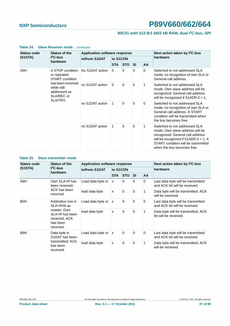
NXP Semiconductors P89V660/662/66480C51 with 512 B/1 kB/2 kB RAM, dual I2C-bus, SPI
A0H A STOP condition or repeated START condition has been received while still addressed as SLA/REC or SLA/TRX.
No S1DAT action 0 0 0 0 Switched to not addressed SLA mode; no recognition of own SLA or General call address.
no S1DAT action 0 0 0 1 Switched to not addressed SLA mode; Own slave address will be recognized; General call address will be recognized if S1ADR.0 = 1.
no S1DAT action 1 0 0 0 Switched to not addressed SLA mode; no recognition of own SLA or General call address. A START condition will be transmitted when the bus becomes free.
no S1DAT action 1 0 0 1 Switched to not addressed SLA mode; Own slave address will be recognized; General call address will be recognized if S1ADR.0 = 1. A START condition will be transmitted when the bus becomes free.
Table 24. Slave Receiver mode …continued
Status code (S1STA)
Status of the I2C-bus hardware
Application software response Next action taken by I2C-bus hardwareto/from S1DAT to S1CON
STA STO SI AA
Table 25. Slave transmitter mode
Status code (S1STA)
Status of the I2C-bus hardware
Application software response Next action taken by I2C-bus
hardwareto/from S1DAT to S1CON
STA STO SI AA
A8H Own SLA+R has been received; ACK has been returned.
Load data byte or x 0 0 0 Last data byte will be transmitted and ACK bit will be received.
load data byte x 0 0 1 Data byte will be transmitted; ACK will be received.
B0H Arbitration lost in SLA+R/W as master; Own SLA+R has been received, ACK has been returned.
Load data byte or x 0 0 0 Last data byte will be transmitted and ACK bit will be received.
load data byte x 0 0 1 Data byte will be transmitted; ACK bit will be received.
B8H Data byte in S1DAT has been transmitted; ACK has been received.
Load data byte or x 0 0 0 Last data byte will be transmitted and ACK bit will be received
load data byte x 0 0 1 Data byte will be transmitted; ACK will be received.
P89V660_662_664 All information provided in this document is subject to legal disclaimers. © NXP B.V. 2011. All rights reserved.
Product data sheet Rev. 3.1 — 17 October 2011 37 of 90
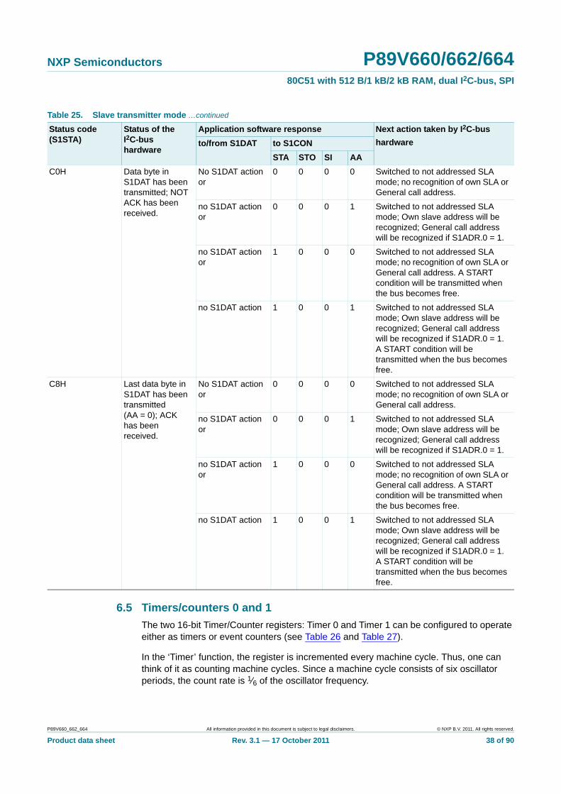
NXP Semiconductors P89V660/662/66480C51 with 512 B/1 kB/2 kB RAM, dual I2C-bus, SPI
6.5 Timers/counters 0 and 1
The two 16-bit Timer/Counter registers: Timer 0 and Timer 1 can be configured to operate either as timers or event counters (see Table 26 and Table 27).
In the ‘Timer’ function, the register is incremented every machine cycle. Thus, one can think of it as counting machine cycles. Since a machine cycle consists of six oscillator periods, the count rate is 1⁄6 of the oscillator frequency.
C0H Data byte in S1DAT has been transmitted; NOT ACK has been received.
No S1DAT action or
0 0 0 0 Switched to not addressed SLA mode; no recognition of own SLA or General call address.
no S1DAT action or
0 0 0 1 Switched to not addressed SLA mode; Own slave address will be recognized; General call address will be recognized if S1ADR.0 = 1.
no S1DAT action or
1 0 0 0 Switched to not addressed SLA mode; no recognition of own SLA or General call address. A START condition will be transmitted when the bus becomes free.
no S1DAT action 1 0 0 1 Switched to not addressed SLA mode; Own slave address will be recognized; General call address will be recognized if S1ADR.0 = 1. A START condition will be transmitted when the bus becomes free.
C8H Last data byte in S1DAT has been transmitted (AA = 0); ACK has been received.
No S1DAT action or
0 0 0 0 Switched to not addressed SLA mode; no recognition of own SLA or General call address.
no S1DAT action or
0 0 0 1 Switched to not addressed SLA mode; Own slave address will be recognized; General call address will be recognized if S1ADR.0 = 1.
no S1DAT action or
1 0 0 0 Switched to not addressed SLA mode; no recognition of own SLA or General call address. A START condition will be transmitted when the bus becomes free.
no S1DAT action 1 0 0 1 Switched to not addressed SLA mode; Own slave address will be recognized; General call address will be recognized if S1ADR.0 = 1. A START condition will be transmitted when the bus becomes free.
Table 25. Slave transmitter mode …continued
Status code (S1STA)
Status of the I2C-bus hardware
Application software response Next action taken by I2C-bus
hardwareto/from S1DAT to S1CON
STA STO SI AA
P89V660_662_664 All information provided in this document is subject to legal disclaimers. © NXP B.V. 2011. All rights reserved.
Product data sheet Rev. 3.1 — 17 October 2011 38 of 90
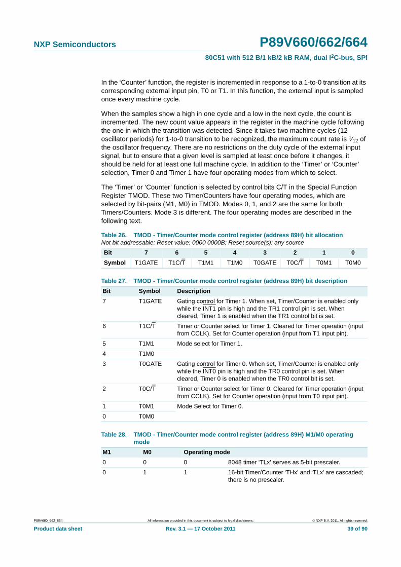
NXP Semiconductors P89V660/662/66480C51 with 512 B/1 kB/2 kB RAM, dual I2C-bus, SPI
In the ‘Counter’ function, the register is incremented in response to a 1-to-0 transition at its corresponding external input pin, T0 or T1. In this function, the external input is sampled once every machine cycle.
When the samples show a high in one cycle and a low in the next cycle, the count is incremented. The new count value appears in the register in the machine cycle following the one in which the transition was detected. Since it takes two machine cycles (12 oscillator periods) for 1-to-0 transition to be recognized, the maximum count rate is 1⁄12 of the oscillator frequency. There are no restrictions on the duty cycle of the external input signal, but to ensure that a given level is sampled at least once before it changes, it should be held for at least one full machine cycle. In addition to the ‘Timer’ or ‘Counter’ selection, Timer 0 and Timer 1 have four operating modes from which to select.
The ‘Timer’ or ‘Counter’ function is selected by control bits C/T in the Special Function Register TMOD. These two Timer/Counters have four operating modes, which are selected by bit-pairs (M1, M0) in TMOD. Modes 0, 1, and 2 are the same for both Timers/Counters. Mode 3 is different. The four operating modes are described in the following text.
Table 26. TMOD - Timer/Counter mode control register (address 89H) bit allocationNot bit addressable; Reset value: 0000 0000B; Reset source(s): any source
Bit 7 6 5 4 3 2 1 0
Symbol T1GATE T1C/T T1M1 T1M0 T0GATE T0C/T T0M1 T0M0
Table 27. TMOD - Timer/Counter mode control register (address 89H) bit description
Bit Symbol Description
7 T1GATE Gating control for Timer 1. When set, Timer/Counter is enabled only while the INT1 pin is high and the TR1 control pin is set. When cleared, Timer 1 is enabled when the TR1 control bit is set.
6 T1C/T Timer or Counter select for Timer 1. Cleared for Timer operation (input from CCLK). Set for Counter operation (input from T1 input pin).
5 T1M1 Mode select for Timer 1.
4 T1M0
3 T0GATE Gating control for Timer 0. When set, Timer/Counter is enabled only while the INT0 pin is high and the TR0 control pin is set. When cleared, Timer 0 is enabled when the TR0 control bit is set.
2 T0C/T Timer or Counter select for Timer 0. Cleared for Timer operation (input from CCLK). Set for Counter operation (input from T0 input pin).
1 T0M1 Mode Select for Timer 0.
0 T0M0
Table 28. TMOD - Timer/Counter mode control register (address 89H) M1/M0 operating mode
M1 M0 Operating mode
0 0 0 8048 timer ‘TLx’ serves as 5-bit prescaler.
0 1 1 16-bit Timer/Counter ‘THx’ and ‘TLx' are cascaded; there is no prescaler.
P89V660_662_664 All information provided in this document is subject to legal disclaimers. © NXP B.V. 2011. All rights reserved.
Product data sheet Rev. 3.1 — 17 October 2011 39 of 90
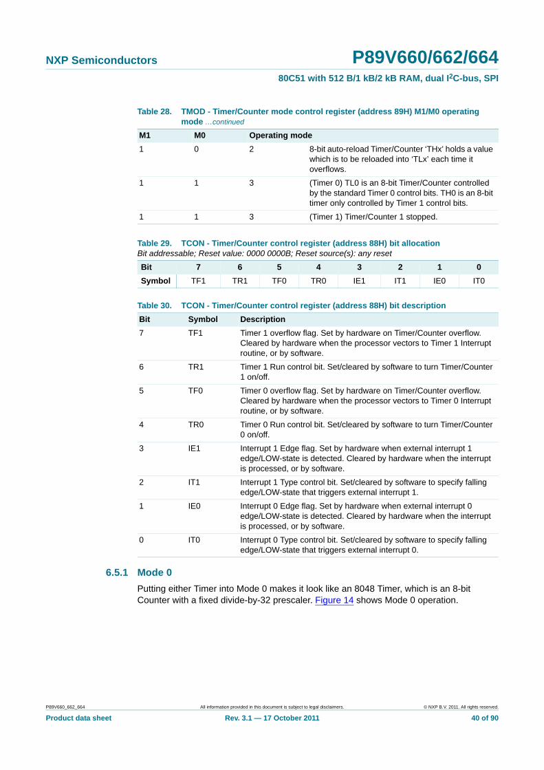
NXP Semiconductors P89V660/662/66480C51 with 512 B/1 kB/2 kB RAM, dual I2C-bus, SPI
6.5.1 Mode 0
Putting either Timer into Mode 0 makes it look like an 8048 Timer, which is an 8-bit Counter with a fixed divide-by-32 prescaler. Figure 14 shows Mode 0 operation.
1 0 2 8-bit auto-reload Timer/Counter ‘THx’ holds a value which is to be reloaded into ‘TLx’ each time it overflows.
1 1 3 (Timer 0) TL0 is an 8-bit Timer/Counter controlled by the standard Timer 0 control bits. TH0 is an 8-bit timer only controlled by Timer 1 control bits.
1 1 3 (Timer 1) Timer/Counter 1 stopped.
Table 29. TCON - Timer/Counter control register (address 88H) bit allocationBit addressable; Reset value: 0000 0000B; Reset source(s): any reset
Bit 7 6 5 4 3 2 1 0
Symbol TF1 TR1 TF0 TR0 IE1 IT1 IE0 IT0
Table 30. TCON - Timer/Counter control register (address 88H) bit description
Bit Symbol Description
7 TF1 Timer 1 overflow flag. Set by hardware on Timer/Counter overflow. Cleared by hardware when the processor vectors to Timer 1 Interrupt routine, or by software.
6 TR1 Timer 1 Run control bit. Set/cleared by software to turn Timer/Counter 1 on/off.
5 TF0 Timer 0 overflow flag. Set by hardware on Timer/Counter overflow. Cleared by hardware when the processor vectors to Timer 0 Interrupt routine, or by software.
4 TR0 Timer 0 Run control bit. Set/cleared by software to turn Timer/Counter 0 on/off.
3 IE1 Interrupt 1 Edge flag. Set by hardware when external interrupt 1 edge/LOW-state is detected. Cleared by hardware when the interrupt is processed, or by software.
2 IT1 Interrupt 1 Type control bit. Set/cleared by software to specify falling edge/LOW-state that triggers external interrupt 1.
1 IE0 Interrupt 0 Edge flag. Set by hardware when external interrupt 0 edge/LOW-state is detected. Cleared by hardware when the interrupt is processed, or by software.
0 IT0 Interrupt 0 Type control bit. Set/cleared by software to specify falling edge/LOW-state that triggers external interrupt 0.
Table 28. TMOD - Timer/Counter mode control register (address 89H) M1/M0 operating mode …continued
M1 M0 Operating mode
P89V660_662_664 All information provided in this document is subject to legal disclaimers. © NXP B.V. 2011. All rights reserved.
Product data sheet Rev. 3.1 — 17 October 2011 40 of 90

NXP Semiconductors P89V660/662/66480C51 with 512 B/1 kB/2 kB RAM, dual I2C-bus, SPI
In this mode, the Timer register is configured as a 13-bit register. As the count rolls over from all 1s to all 0s, it sets the Timer interrupt flag TFn. The count input is enabled to the Timer when TRn = 1 and either GATE = 0 or INTn = 1. (Setting GATE = 1 allows the Timer to be controlled by external input INTn, to facilitate pulse width measurements). TRn is a control bit in the Special Function Register TCON (Figure 5). The GATE bit is in the TMOD register.
The 13-bit register consists of all 8 bits of THn and the lower 5 bits of TLn. The upper 3 bits of TLn are indeterminate and should be ignored. Setting the run flag (TRn) does not clear the registers.
Mode 0 operation is the same for Timer 0 and Timer 1 (see Figure 14). There are two different GATE bits, one for Timer 1 (TMOD.7) and one for Timer 0 (TMOD.3).
6.5.2 Mode 1
Mode 1 is the same as Mode 0, except that all 16 bits of the timer register (THn and TLn) are used. See Figure 15.
6.5.3 Mode 2
Mode 2 configures the Timer register as an 8-bit Counter (TLn) with automatic reload, as shown in Figure 16. Overflow from TLn not only sets TFn, but also reloads TLn with the contents of THn, which must be preset by software. The reload leaves THn unchanged. Mode 2 operation is the same for Timer 0 and Timer 1.
Fig 14. Timer/Counter 0 or 1 in Mode 0 (13-bit counter)
002aaa519
osc/6Tn pin
TRn
TnGate
INTn pin
C/T = 0
C/T = 1
TLn(5-bits)
THn(8-bits)
TFncontrol
overflow
interrupt
Fig 15. Timer/Counter 0 or 1 in Mode 1 (16-bit counter)
002aaa520
osc/6Tn pin
TRn
TnGate
INTn pin
C/T = 0
C/T = 1
TLn(8-bits)
THn(8-bits)
TFncontrol
overflow
interrupt
P89V660_662_664 All information provided in this document is subject to legal disclaimers. © NXP B.V. 2011. All rights reserved.
Product data sheet Rev. 3.1 — 17 October 2011 41 of 90
NXP Semiconductors P89V660/662/66480C51 with 512 B/1 kB/2 kB RAM, dual I2C-bus, SPI
6.5.4 Mode 3
When timer 1 is in Mode 3 it is stopped (holds its count). The effect is the same as setting TR1 = 0.
Timer 0 in Mode 3 establishes TL0 and TH0 as two separate 8-bit counters. The logic for Mode 3 and Timer 0 is shown in Figure 17. TL0 uses the Timer 0 control bits: T0C/T, T0GATE, TR0, INT0, and TF0. TH0 is locked into a timer function (counting machine cycles) and takes over the use of TR1 and TF1 from Timer 1. Thus, TH0 now controls the ‘Timer 1’ interrupt.
Mode 3 is provided for applications that require an extra 8-bit timer. With Timer 0 in Mode 3, the P89V660/662/664 can look like it has an additional Timer.
Note: When Timer 0 is in Mode 3, Timer 1 can be turned on and off by switching it into and out of its own Mode 3. It can still be used by the serial port as a baud rate generator, or in any application not requiring an interrupt.
6.6 Timer 2
Timer 2 is a 16-bit Timer/Counter which can operate as either an event timer or an event counter, as selected by C/T2 in the special function register T2CON. Timer 2 has four operating modes: Capture, Auto-reload (up or down counting), Clock-out, and Baud Rate Generator which are selected according to Table 31 using T2CON (Table 32 and Table 33) and T2MOD (Table 34 and Table 35).
Fig 16. Timer/Counter 0 or 1 in Mode 2 (8-bit auto-reload)
002aaa521
osc/6Tn pin
TRn
TnGate
INTn pin
TLn(8-bits)
THn(8-bits)
TFncontrol
overflow
reload
interrupt
C/T = 0
C/T = 1
Fig 17. Timer/Counter 0 Mode 3 (two 8-bit counters)
002aaa522
osc/2
TR1
TR0
TnGate
INT0 pin
TL0(8-bits)
TF0control
overflowinterrupt
TH0(8-bits)
TF1control
overflowinterrupt
osc/6T0 pin
C/T = 0
C/T = 1
P89V660_662_664 All information provided in this document is subject to legal disclaimers. © NXP B.V. 2011. All rights reserved.
Product data sheet Rev. 3.1 — 17 October 2011 42 of 90
NXP Semiconductors P89V660/662/66480C51 with 512 B/1 kB/2 kB RAM, dual I2C-bus, SPI
Table 31. Timer 2 operating mode
RCLK+TCLK CP/RL2 TR2 T2OE Mode
0 0 1 0 16-bit auto reload
0 1 1 0 16-bit capture
0 0 1 1 Programmable Clock-Out
1 X 1 0 Baud rate generator
X X 0 X off
Table 32. T2CON - Timer/Counter 2 control register (address C8H) bit allocationBit addressable; Reset value: 00H
Bit 7 6 5 4 3 2 1 0
Symbol TF2 EXF2 RCLK TCLK EXEN2 TR2 C/T2 CP/RL2
Table 33. T2CON - Timer/Counter 2 control register (address C8H) bit description
Bit Symbol Description
7 TF2 Timer 2 overflow flag set by a Timer 2 overflow and must be cleared by software. TF2 will not be set when either RCLK or TCLK = 1 or when Timer 2 is in Clock-out mode.
6 EXF2 Timer 2 external flag is set when Timer 2 is in capture, reload or baud rate mode, EXEN2 = 1 and a negative transition on T2EX occurs. If Timer 2 interrupt is enabled EXF2 = 1 causes the CPU to vector to the Timer 2 interrupt routine. EXF2 must be cleared by software.
5 RCLK Receive clock flag. When set, causes the UART to use Timer 2 overflow pulses for its receive clock in modes 1 and 3. RCLK = 0 causes Timer 1 overflow to be used for the receive clock.
4 TCLK Transmit clock flag. When set, causes the UART to use Timer 2 overflow pulses for its transmit clock in modes 1 and 3. TCLK = 0 causes Timer 1 overflows to be used for the transmit clock.
3 EXEN2 Timer 2 external enable flag. When set, allows a capture or reload to occur as a result of a negative transition on T2EX if Timer 2 is not being used to clock the serial port. EXEN2 = 0 causes Timer 2 to ignore events at T2EX.
2 TR2 Start/stop control for Timer 2. A logic ‘1’ enables the timer to run.
1 C/T2 Timer or counter select. (Timer 2)
0 = internal timer (fosc / 6)
1 = external event counter (falling edge triggered; external clock’s maximum rate = fosc / 12.
0 CP/RL2 Capture/Reload flag. When set, captures will occur on negative transitions at T2EX if EXEN2 = 1. When cleared, auto-reloads will occur either with Timer 2 overflows or negative transitions at T2EX when EXEN2 = 1. When either RCLK = 1 or TCLK = 1, this bit is ignored and the timer is forced to auto-reload on Timer 2 overflow.
Table 34. T2MOD - Timer 2 mode control register (address C9H) bit allocationNot bit addressable; Reset value: XX00 0000B
Bit 7 6 5 4 3 2 1 0
Symbol - - - - - - T2OE DCEN
P89V660_662_664 All information provided in this document is subject to legal disclaimers. © NXP B.V. 2011. All rights reserved.
Product data sheet Rev. 3.1 — 17 October 2011 43 of 90
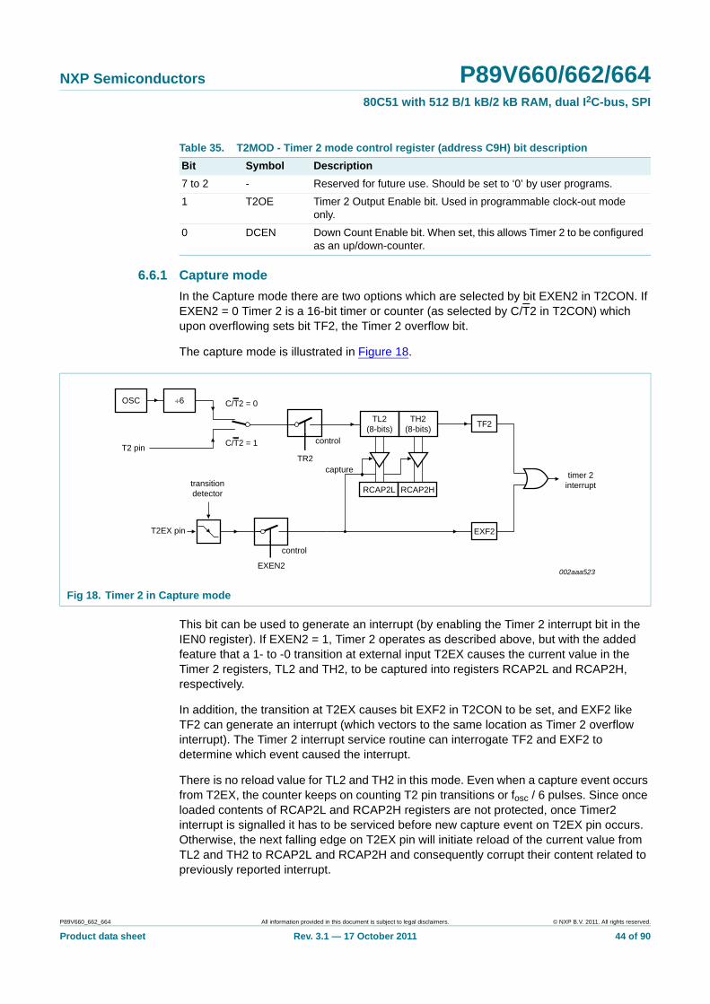
NXP Semiconductors P89V660/662/66480C51 with 512 B/1 kB/2 kB RAM, dual I2C-bus, SPI
6.6.1 Capture mode
In the Capture mode there are two options which are selected by bit EXEN2 in T2CON. If EXEN2 = 0 Timer 2 is a 16-bit timer or counter (as selected by C/T2 in T2CON) which upon overflowing sets bit TF2, the Timer 2 overflow bit.
The capture mode is illustrated in Figure 18.
This bit can be used to generate an interrupt (by enabling the Timer 2 interrupt bit in the IEN0 register). If EXEN2 = 1, Timer 2 operates as described above, but with the added feature that a 1- to -0 transition at external input T2EX causes the current value in the Timer 2 registers, TL2 and TH2, to be captured into registers RCAP2L and RCAP2H, respectively.
In addition, the transition at T2EX causes bit EXF2 in T2CON to be set, and EXF2 like TF2 can generate an interrupt (which vectors to the same location as Timer 2 overflow interrupt). The Timer 2 interrupt service routine can interrogate TF2 and EXF2 to determine which event caused the interrupt.
There is no reload value for TL2 and TH2 in this mode. Even when a capture event occurs from T2EX, the counter keeps on counting T2 pin transitions or fosc / 6 pulses. Since once loaded contents of RCAP2L and RCAP2H registers are not protected, once Timer2 interrupt is signalled it has to be serviced before new capture event on T2EX pin occurs. Otherwise, the next falling edge on T2EX pin will initiate reload of the current value from TL2 and TH2 to RCAP2L and RCAP2H and consequently corrupt their content related to previously reported interrupt.
Table 35. T2MOD - Timer 2 mode control register (address C9H) bit description
Bit Symbol Description
7 to 2 - Reserved for future use. Should be set to ‘0’ by user programs.
1 T2OE Timer 2 Output Enable bit. Used in programmable clock-out mode only.
0 DCEN Down Count Enable bit. When set, this allows Timer 2 to be configured as an up/down-counter.
Fig 18. Timer 2 in Capture mode
002aaa523
OSC ÷6
T2 pin
C/T2 = 0
C/T2 = 1
TL2(8-bits)
TH2(8-bits)
TF2
control
captureTR2
timer 2interrupt
EXF2
RCAP2L RCAP2H
control
EXEN2
transitiondetector
T2EX pin
P89V660_662_664 All information provided in this document is subject to legal disclaimers. © NXP B.V. 2011. All rights reserved.
Product data sheet Rev. 3.1 — 17 October 2011 44 of 90

NXP Semiconductors P89V660/662/66480C51 with 512 B/1 kB/2 kB RAM, dual I2C-bus, SPI
6.6.2 Auto-reload mode (up or down-counter)
In the 16-bit auto-reload mode, Timer 2 can be configured as either a timer or counter (via C/T2 in T2CON), then programmed to count up or down. The counting direction is determined by bit DCEN (Down-counter Enable) which is located in the T2MOD register (see Table 34 and Table 35). When reset is applied, DCEN = 0 and Timer 2 will default to counting up. If the DCEN bit is set, Timer 2 can count up or down depending on the value of the T2EX pin.
Figure 19 shows Timer 2 counting up automatically (DCEN = 0).
In this mode, there are two options selected by bit EXEN2 in T2CON register. If EXEN2 = 0, then Timer 2 counts up to 0FFFFH and sets the TF2 (Overflow Flag) bit upon overflow. This causes the Timer 2 registers to be reloaded with the 16-bit value in RCAP2L and RCAP2H. The values in RCAP2L and RCAP2H are preset by software means.
Auto reload frequency when Timer 2 is counting up can be determined from this formula:
(1)
Where SupplyFrequency is either fosc (C/T2 = 0) or frequency of signal on T2 pin (C/T2 = 1).
If EXEN2 = 1, a 16-bit reload can be triggered either by an overflow or by a 1-to-0 transition at input T2EX. This transition also sets the EXF2 bit. The Timer 2 interrupt, if enabled, can be generated when either TF2 or EXF2 is ‘1’.
Microcontroller’s hardware will need three consecutive machine cycles in order to recognize falling edge on T2EX and set EXF2 = 1: in the first machine cycle pin T2EX has to be sampled as ‘1’; in the second machine cycle it has to be sampled as ‘0’, and in the third machine cycle EXF2 will be set to ‘1’.
Fig 19. Timer 2 in Auto-reload mode (DCEN = 0)
002aaa524
OSC ÷6
T2 pin
C/T2 = 0
C/T2 = 1
TL2(8-bits)
TH2(8-bits)
TF2
control
reloadTR2
timer 2interrupt
EXF2
RCAP2L RCAP2H
control
EXEN2
transitiondetector
T2EX pin
SupplyFrequency65536 RCAP2H RCAP2L –----------------------------------------------------------------------------
P89V660_662_664 All information provided in this document is subject to legal disclaimers. © NXP B.V. 2011. All rights reserved.
Product data sheet Rev. 3.1 — 17 October 2011 45 of 90

NXP Semiconductors P89V660/662/66480C51 with 512 B/1 kB/2 kB RAM, dual I2C-bus, SPI
In Figure 20, DCEN = 1 and Timer 2 is enabled to count up or down. This mode allows pin T2EX to control the direction of count. When a logic ‘1’ is applied at pin T2EX Timer 2 will count up. Timer 2 will overflow at 0FFFFH and set the TF2 flag, which can then generate an interrupt, if the interrupt is enabled. This timer overflow also causes the 16-bit value in RCAP2L and RCAP2H to be reloaded into the timer registers TL2 and TH2.
When a logic 0 is applied at pin T2EX this causes Timer 2 to count down. The timer will underflow when TL2 and TH2 become equal to the value stored in RCAP2L and RCAP2H. Timer 2 underflow sets the TF2 flag and causes 0FFFFH to be reloaded into the timer registers TL2 and TH2. The external flag EXF2 toggles when Timer 2 underflows or overflows. This EXF2 bit can be used as a 17th bit of resolution if needed.
6.6.3 Programmable clock-out
A 50 % duty cycle clock can be programmed to come out on pin T2 (P1[0]). This pin, besides being a regular I/O pin, has two additional functions. It can be programmed:
1. To input the external clock for Timer/Counter 2, or
2. To output a 50 % duty cycle clock ranging from 122 Hz to 8 MHz at a 16 MHz operating frequency.
To configure the Timer/Counter 2 as a clock generator, bit C/T2 (in T2CON) must be cleared and bit T20E in T2MOD must be set. Bit TR2 (T2CON.2) also must be set to start the timer.
The Clock-Out frequency depends on the oscillator frequency and the reload value of Timer 2 capture registers (RCAP2H, RCAP2L) as shown in Equation 2:
(2)
Where n = 2 (6-clock mode) and n = 4 (12-clock mode);
Where (RCAP2H,RCAP2L) = the content of RCAP2H and RCAP2L taken as a 16-bit unsigned integer.
Fig 20. Timer 2 in Auto Reload mode (DCEN = 1)
002aaa525
TL2(8-bits)
TH2(8-bits)
TF2
EXF2
underflow timer 2interrupt
RCAP2L RCAP2H
FFH FFH
overflow
(down-counting reload value)
(up-counting reload value)
count direction1 = up0 = down
T2EX pin
toggle
OSC ÷6
T2 pin
C/T2 = 0
C/T2 = 1 control
TR2
OscillatorFrequencyn 65536 RCAP2H RCAP2L – ------------------------------------------------------------------------------------------
P89V660_662_664 All information provided in this document is subject to legal disclaimers. © NXP B.V. 2011. All rights reserved.
Product data sheet Rev. 3.1 — 17 October 2011 46 of 90
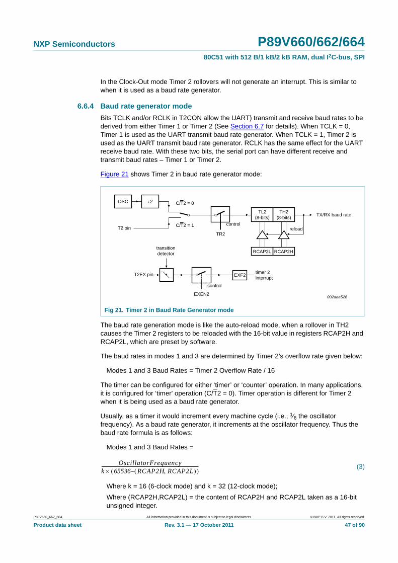
NXP Semiconductors P89V660/662/66480C51 with 512 B/1 kB/2 kB RAM, dual I2C-bus, SPI
In the Clock-Out mode Timer 2 rollovers will not generate an interrupt. This is similar to when it is used as a baud rate generator.
6.6.4 Baud rate generator mode
Bits TCLK and/or RCLK in T2CON allow the UART) transmit and receive baud rates to be derived from either Timer 1 or Timer 2 (See Section 6.7 for details). When TCLK = 0, Timer 1 is used as the UART transmit baud rate generator. When TCLK = 1, Timer 2 is used as the UART transmit baud rate generator. RCLK has the same effect for the UART receive baud rate. With these two bits, the serial port can have different receive and transmit baud rates – Timer 1 or Timer 2.
Figure 21 shows Timer 2 in baud rate generator mode:
The baud rate generation mode is like the auto-reload mode, when a rollover in TH2 causes the Timer 2 registers to be reloaded with the 16-bit value in registers RCAP2H and RCAP2L, which are preset by software.
The baud rates in modes 1 and 3 are determined by Timer 2’s overflow rate given below:
Modes 1 and 3 Baud Rates = Timer 2 Overflow Rate / 16
The timer can be configured for either ‘timer’ or ‘counter’ operation. In many applications, it is configured for ‘timer' operation (C/T2 = 0). Timer operation is different for Timer 2 when it is being used as a baud rate generator.
Usually, as a timer it would increment every machine cycle (i.e., 1⁄6 the oscillator frequency). As a baud rate generator, it increments at the oscillator frequency. Thus the baud rate formula is as follows:
Modes 1 and 3 Baud Rates =
(3)
Where k = 16 (6-clock mode) and k = 32 (12-clock mode);
Where (RCAP2H,RCAP2L) = the content of RCAP2H and RCAP2L taken as a 16-bit unsigned integer.
Fig 21. Timer 2 in Baud Rate Generator mode
002aaa526
TX/RX baud rate
timer 2interrupt
OSC ÷2
T2 pin
C/T2 = 0
C/T2 = 1
TL2(8-bits)
TH2(8-bits)
control
TR2
EXF2
RCAP2L RCAP2H
control
EXEN2
transitiondetector
T2EX pin
reload
OscillatorFrequencyk 65536 RCAP2H RCAP2L – ---------------------------------------------------------------------------------------
P89V660_662_664 All information provided in this document is subject to legal disclaimers. © NXP B.V. 2011. All rights reserved.
Product data sheet Rev. 3.1 — 17 October 2011 47 of 90
NXP Semiconductors P89V660/662/66480C51 with 512 B/1 kB/2 kB RAM, dual I2C-bus, SPI
The Timer 2 as a baud rate generator mode is valid only if RCLK and/or TCLK = 1 in T2CON register. Note that a rollover in TH2 does not set TF2, and will not generate an interrupt. Thus, the Timer 2 interrupt does not have to be disabled when Timer 2 is in the baud rate generator mode. Also if the EXEN2 (T2 external enable flag) is set, a 1-to-0 transition in T2EX (Timer/counter 2 trigger input) will set EXF2 (T2 external flag) but will not cause a reload from (RCAP2H, RCAP2L) to (TH2,TL2). Therefore when Timer 2 is in use as a baud rate generator, T2EX can be used as an additional external interrupt, if needed.
When Timer 2 is in the baud rate generator mode, one should not try to read or write TH2 and TL2. Under these conditions, a read or write of TH2 or TL2 may not be accurate. The RCAP2 registers may be read, but should not be written to, because a write might overlap a reload and cause write and/or reload errors. The timer should be turned off (clear TR2) before accessing the Timer 2 or RCAP2 registers. Table 36 shows commonly used baud rates and how they can be obtained from Timer 2.
6.6.5 Summary of baud rate equations
Timer 2 is in baud rate generating mode. If Timer 2 is being clocked through pin T2 (P1[0]) the baud rate is:
Baud rate = Timer 2 overflow rate / 16
If Timer 2 is being clocked internally, the baud rate is:
Baud rate = fosc / (16 (65536 (RCAP2H, RCAP2L)))
Where fosc = oscillator frequency
To obtain the reload value for RCAP2H and RCAP2L, the above equation can be rewritten as:
RCAP2H, RCAP2L = 65536 fosc / (16 baud rate)
6.7 UARTs
The UART operates in all standard modes. Enhancements over the standard 80C51 UART include Framing Error detection, and automatic address recognition.
Table 36. Timer 2 generated commonly used baud rates
Rate Oscillator frequency Timer 2
RCAP2H RCAP2L
750 kBd 12 MHz FF FF
19.2 kBd 12 MHz FF D9
9.6 kBd 12 MHz FF B2
4.8 kBd 12 MHz FF 64
2.4 kBd 12 MHz FE C8
600 Bd 12 MHz FB 1E
220 Bd 12 MHz F2 AF
600 Bd 6 MHz FD 8F
220 Bd 6 MHz F9 57
P89V660_662_664 All information provided in this document is subject to legal disclaimers. © NXP B.V. 2011. All rights reserved.
Product data sheet Rev. 3.1 — 17 October 2011 48 of 90
NXP Semiconductors P89V660/662/66480C51 with 512 B/1 kB/2 kB RAM, dual I2C-bus, SPI
6.7.1 Mode 0
Serial data enters and exits through RXD and TXD outputs the shift clock. Only 8 bits are transmitted or received, LSB first. The baud rate is fixed at 1⁄6 of the CPU clock frequency. UART configured to operate in this mode outputs serial clock on TXD line no matter whether it sends or receives data on RXD line.
6.7.2 Mode 1
10 bits are transmitted (through TXD) or received (through RXD): a start bit (logical 0), 8 data bits (LSB first), and a stop bit (logical 1). When data is received, the stop bit is stored in RB8 in Special Function Register SCON. The baud rate is variable and is determined by the Timer 1⁄2 overflow rate.
6.7.3 Mode 2
11 bits are transmitted (through TXD) or received (through RXD): start bit (logical 0), 8 data bits (LSB first), a programmable 9th data bit, and a stop bit (logical 1). When data is transmitted, the 9th data bit (TB8 in SCON) can be assigned the value of 0 or (e.g. the parity bit (P, in the PSW) could be moved into TB8). When data is received, the 9th data bit goes into RB8 in Special Function Register SCON, while the stop bit is ignored. The baud rate is programmable to either 1⁄16 or 1⁄32 of the CPU clock frequency, as determined by the SMOD1 bit in PCON.
6.7.4 Mode 3
11 bits are transmitted (through TXD) or received (through RXD): a start bit (logical 0), 8 data bits (LSB first), a programmable 9th data bit, and a stop bit (logical 1). In fact, Mode 3 is the same as Mode 2 in all respects except baud rate. The baud rate in Mode 3 is variable and is determined by the Timer 1⁄2 overflow rate.
Table 37. SCON - Serial port control register (address 98H) bit allocationBit addressable; Reset value: 00H
Bit 7 6 5 4 3 2 1 0
Symbol SM0/FE SM1 SM2 REN TB8 RB8 TI RI
Table 38. SCON - Serial port control register (address 98H) bit description
Bit Symbol Description
7 SM0/FE The usage of this bit is determined by SMOD0 in the PCON register. If SMOD0 = 0, this bit is SM0, which with SM1, defines the serial port mode. If SMOD0 = 1, this bit is FE (Framing Error). FE is set by the receiver when an invalid stop bit is detected. Once set, this bit cannot be cleared by valid frames but can only be cleared by software. (Note: It is recommended to set up UART mode bits SM0 and SM1 before setting SMOD0 to ‘1’.)
6 SM1 With SM0, defines the serial port mode (see Table 39 below).
5 SM2 Enables the multiprocessor communication feature in Modes 2 and 3. In Mode 2 or 3, if SM2 is set to ‘1’, then Rl will not be activated if the received 9th data bit (RB8) is ‘0’. In Mode 1, if SM2 = 1 then RI will not be activated if a valid stop bit was not received. In Mode 0, SM2 should be ‘0’.
4 REN Enables serial reception. Set by software to enable reception. Clear by software to disable reception.
P89V660_662_664 All information provided in this document is subject to legal disclaimers. © NXP B.V. 2011. All rights reserved.
Product data sheet Rev. 3.1 — 17 October 2011 49 of 90
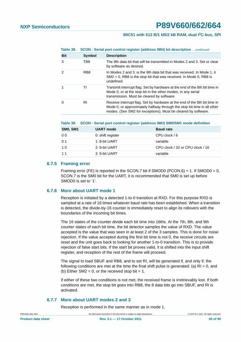
NXP Semiconductors P89V660/662/66480C51 with 512 B/1 kB/2 kB RAM, dual I2C-bus, SPI
6.7.5 Framing error
Framing error (FE) is reported in the SCON.7 bit if SMOD0 (PCON.6) = 1. If SMOD0 = 0, SCON.7 is the SM0 bit for the UART, it is recommended that SM0 is set up before SMOD0 is set to ‘1’.
6.7.6 More about UART mode 1
Reception is initiated by a detected 1-to-0 transition at RXD. For this purpose RXD is sampled at a rate of 16 times whatever baud rate has been established. When a transition is detected, the divide-by-16 counter is immediately reset to align its rollovers with the boundaries of the incoming bit times.
The 16 states of the counter divide each bit time into 16ths. At the 7th, 8th, and 9th counter states of each bit time, the bit detector samples the value of RXD. The value accepted is the value that was seen in at least 2 of the 3 samples. This is done for noise rejection. If the value accepted during the first bit time is not 0, the receive circuits are reset and the unit goes back to looking for another 1-to-0 transition. This is to provide rejection of false start bits. If the start bit proves valid, it is shifted into the input shift register, and reception of the rest of the frame will proceed.
The signal to load SBUF and RB8, and to set RI, will be generated if, and only if, the following conditions are met at the time the final shift pulse is generated: (a) RI = 0, and (b) Either SM2 = 0, or the received stop bit = 1.
If either of these two conditions is not met, the received frame is irretrievably lost. If both conditions are met, the stop bit goes into RB8, the 8 data bits go into SBUF, and RI is activated.
6.7.7 More about UART modes 2 and 3
Reception is performed in the same manner as in mode 1.
3 TB8 The 9th data bit that will be transmitted in Modes 2 and 3. Set or clear by software as desired.
2 RB8 In Modes 2 and 3, is the 9th data bit that was received. In Mode 1, it SM2 = 0, RB8 is the stop bit that was received. In Mode 0, RB8 is undefined.
1 TI Transmit interrupt flag. Set by hardware at the end of the 8th bit time in Mode 0, or at the stop bit in the other modes, in any serial transmission. Must be cleared by software.
0 RI Receive interrupt flag. Set by hardware at the end of the 8th bit time in Mode 0, or approximately halfway through the stop bit time in all other modes. (See SM2 for exceptions). Must be cleared by software.
Table 39. SCON - Serial port control register (address 98H) SM0/SM1 mode definition
SM0, SM1 UART mode Baud rate
0 0 0: shift register CPU clock / 6
0 1 1: 8-bit UART variable
1 0 2: 9-bit UART CPU clock / 32 or CPU clock / 16
1 1 3: 9-bit UART variable
Table 38. SCON - Serial port control register (address 98H) bit description …continued
Bit Symbol Description
P89V660_662_664 All information provided in this document is subject to legal disclaimers. © NXP B.V. 2011. All rights reserved.
Product data sheet Rev. 3.1 — 17 October 2011 50 of 90

NXP Semiconductors P89V660/662/66480C51 with 512 B/1 kB/2 kB RAM, dual I2C-bus, SPI
The signal to load SBUF and RB8, and to set RI, will be generated if, and only if, the following conditions are met at the time the final shift pulse is generated: (a) RI = 0, and (b) Either SM2 = 0, or the received 9th data bit = 1.
If either of these conditions is not met, the received frame is irretrievably lost, and RI is not set. If both conditions are met, the received 9th data bit goes into RB8, and the first 8 data bits go into SBUF.
6.7.8 Multiprocessor communications
UART modes 2 and 3 have a special provision for multiprocessor communications. In these modes, 9 data bits are received or transmitted. When data is received, the 9th bit is stored in RB8. The UART can be programmed so that when the stop bit is received, the serial port interrupt will be activated only if RB8 = 1. This feature is enabled by setting bit SM2 in SCON. One way to use this feature in multiprocessor systems is as follows:
When the master processor wants to transmit a block of data to one of several slaves, it first sends out an address byte which identifies the target slave. An address byte differs from a data byte in a way that the 9th bit is ‘1’ in an address byte and ‘0’ in the data byte. With SM2 = 1, no slave will be interrupted by a data byte, i.e. the received 9th bit is ‘0’. However, an address byte having the 9th bit set to ‘1’ will interrupt all slaves, so that each slave can examine the received byte and see if it is being addressed or not. The addressed slave will clear its SM2 bit and prepare to receive the data (still 9 bits long) that follow. The slaves that weren’t being addressed leave their SM2 bits set and go on about their business, ignoring the subsequent data bytes.
SM2 has no effect in Mode 0, and in Mode 1 can be used to check the validity of the stop bit, although this is better done with the Framing Error flag. When UART receives data in mode 1 and SM2 = 1, the receive interrupt will not be activated unless a valid stop bit is received.
6.7.9 Automatic address recognition
Automatic address recognition is a feature which allows the UART to recognize certain addresses in the serial bit stream by using hardware to make the comparisons. This feature saves a great deal of software overhead by eliminating the need for the software to examine every serial address which passes by the serial port. This feature is enabled for the UART by setting the SM2 bit in SCON. In the 9 bit UART modes, mode 2 and mode 3, the Receive Interrupt flag (RI) will be automatically set when the received byte contains either the ‘Given’ address or the ‘Broadcast' address. The 9 bit mode requires that the 9th information bit is a ‘1’ to indicate that the received information is an address and not data.
Using the automatic address recognition feature allows a master to selectively communicate with one or more slaves by invoking the Given slave address or addresses. All of the slaves may be contacted by using the Broadcast address. Two special function registers are used to define the slave’s address, SADDR, and the address mask, SADEN. SADEN is used to define which bits in the SADDR are to be used and which bits are ‘don’t care’. The SADEN mask can be logically ANDed with the SADDR to create the Given address which the master will use for addressing each of the slaves. Use of the Given address allows multiple slaves to be recognized while excluding others.
This device uses the methods presented in Figure 22 to determine if a Given or Broadcast address has been received or not.
P89V660_662_664 All information provided in this document is subject to legal disclaimers. © NXP B.V. 2011. All rights reserved.
Product data sheet Rev. 3.1 — 17 October 2011 51 of 90
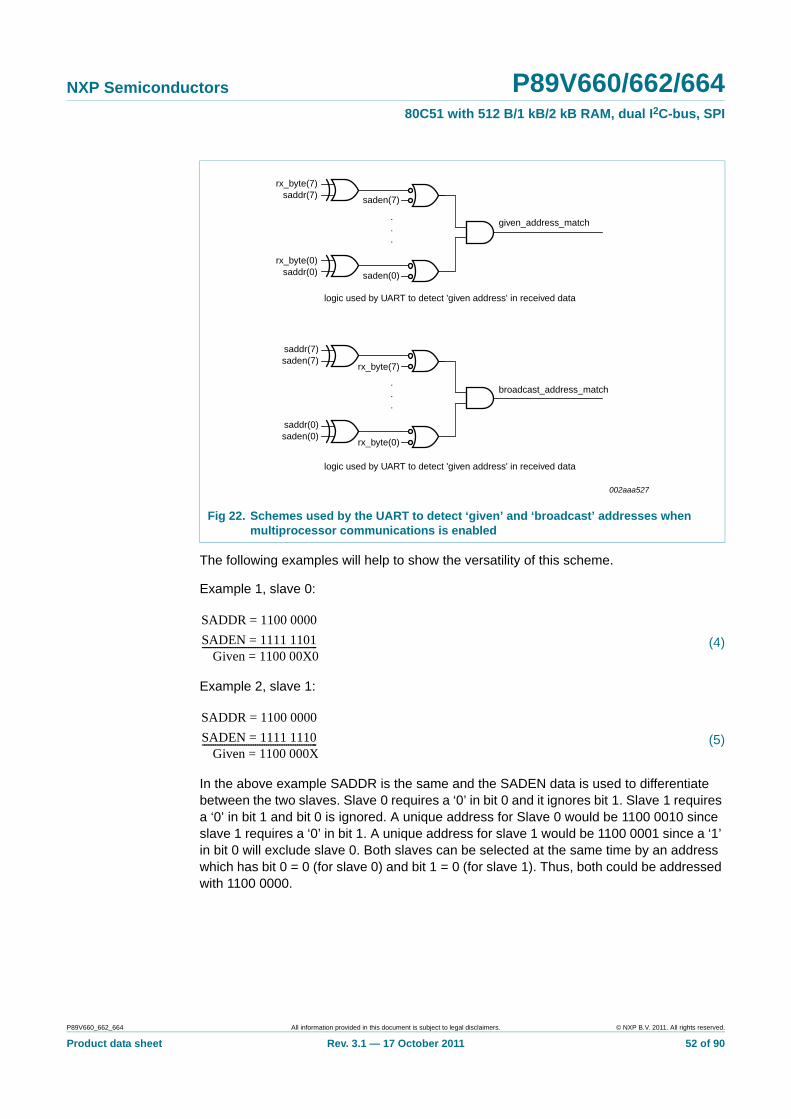
NXP Semiconductors P89V660/662/66480C51 with 512 B/1 kB/2 kB RAM, dual I2C-bus, SPI
The following examples will help to show the versatility of this scheme.
Example 1, slave 0:
(4)
Example 2, slave 1:
(5)
In the above example SADDR is the same and the SADEN data is used to differentiate between the two slaves. Slave 0 requires a ‘0’ in bit 0 and it ignores bit 1. Slave 1 requires a ‘0’ in bit 1 and bit 0 is ignored. A unique address for Slave 0 would be 1100 0010 since slave 1 requires a ‘0’ in bit 1. A unique address for slave 1 would be 1100 0001 since a ‘1’ in bit 0 will exclude slave 0. Both slaves can be selected at the same time by an address which has bit 0 = 0 (for slave 0) and bit 1 = 0 (for slave 1). Thus, both could be addressed with 1100 0000.
Fig 22. Schemes used by the UART to detect ‘given’ and ‘broadcast’ addresses when multiprocessor communications is enabled
002aaa527
rx_byte(7)saddr(7) saden(7)
rx_byte(0)saddr(0)
.
.
.
given_address_match
logic used by UART to detect 'given address' in received data
saddr(7)saden(7)
rx_byte(7)
saddr(0)saden(0)
rx_byte(0)
broadcast_address_match
logic used by UART to detect 'given address' in received data
saden(0)
.
.
.
SADDR = 1100 0000
SADEN = 1111 1101Given = 1100 00X0
----------------------------------------------------
SADDR = 1100 0000
SADEN = 1111 1110Given = 1100 000X
----------------------------------------------------
P89V660_662_664 All information provided in this document is subject to legal disclaimers. © NXP B.V. 2011. All rights reserved.
Product data sheet Rev. 3.1 — 17 October 2011 52 of 90
NXP Semiconductors P89V660/662/66480C51 with 512 B/1 kB/2 kB RAM, dual I2C-bus, SPI
In a more complex system the following could be used to select slaves 1 and 2 while excluding slave 0:
Example 1, slave 0:
(6)
Example 2, slave 1:
(7)
Example 2, slave 2:
(8)
In the above example the differentiation among the 3 slaves is in the lower 3 address bits. Slave 0 requires that bit 0 = 0 and it can be uniquely addressed by 1110 0110. Slave 1 requires that bit 1 = 0 and it can be uniquely addressed by 1110 0101. Slave 2 requires that bit 2 = 0 and its unique address is 1110 0011. To select Slaves 0 and 1 and exclude Slave 2 use address 1110 0100, since it is necessary to make bit 2 = 1 to exclude slave 2. The Broadcast Address for each slave is created by taking the logical OR of SADDR and SADEN. Zeros in this result are treated as don’t-cares. In most cases, interpreting the don’t-cares as ones, the broadcast address will be FF hexadecimal. Upon reset SADDR and SADEN are loaded with 0s. This produces a given address of all ‘don’t cares’ as well as a Broadcast address of all ‘don’t cares'. This effectively disables the Automatic Addressing mode and allows the microcontroller to use standard UART drivers which do not make use of this feature.
6.8 Serial Peripheral Interface (SPI)
6.8.1 SPI features
• Master or slave operation
• 10 MHz bit frequency (max)
• LSB first or MSB first data transfer
• Four programmable bit rates
• End of transmission (SPIF)
• Write collision flag protection (WCOL)
• Wake-up from Idle mode (slave mode only)
6.8.2 SPI description
The serial peripheral interface allows high-speed synchronous data transfer between the P89V660/662/664 and peripheral devices or between several P89V660/662/664 devices. Figure 23 shows the correspondence between master and slave SPI devices. The
SADDR = 1100 0000
SADEN = 1111 1001Given = 1100 0XX0
----------------------------------------------------
SADDR = 1110 0000
SADEN = 1111 1010Given = 1110 0X0X
----------------------------------------------------
SADDR = 1100 0000
SADEN = 1111 1100Given = 1100 00XX
----------------------------------------------------
P89V660_662_664 All information provided in this document is subject to legal disclaimers. © NXP B.V. 2011. All rights reserved.
Product data sheet Rev. 3.1 — 17 October 2011 53 of 90
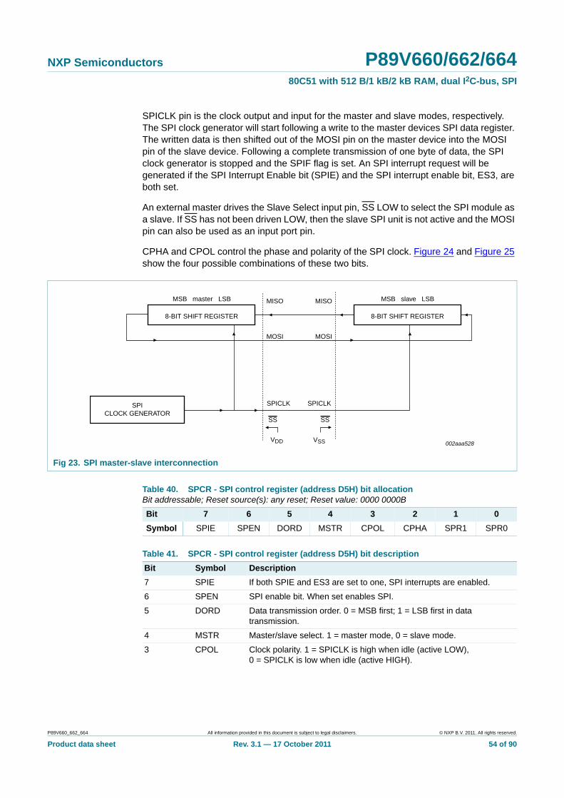
NXP Semiconductors P89V660/662/66480C51 with 512 B/1 kB/2 kB RAM, dual I2C-bus, SPI
SPICLK pin is the clock output and input for the master and slave modes, respectively. The SPI clock generator will start following a write to the master devices SPI data register. The written data is then shifted out of the MOSI pin on the master device into the MOSI pin of the slave device. Following a complete transmission of one byte of data, the SPI clock generator is stopped and the SPIF flag is set. An SPI interrupt request will be generated if the SPI Interrupt Enable bit (SPIE) and the SPI interrupt enable bit, ES3, are both set.
An external master drives the Slave Select input pin, SS LOW to select the SPI module as a slave. If SS has not been driven LOW, then the slave SPI unit is not active and the MOSI pin can also be used as an input port pin.
CPHA and CPOL control the phase and polarity of the SPI clock. Figure 24 and Figure 25 show the four possible combinations of these two bits.
Fig 23. SPI master-slave interconnection
002aaa528
8-BIT SHIFT REGISTER
MSB master LSB
SPICLOCK GENERATOR
MISO MISO
MOSI MOSI
SPICLK SPICLK
SS SS
8-BIT SHIFT REGISTER
MSB slave LSB
VSSVDD
Table 40. SPCR - SPI control register (address D5H) bit allocationBit addressable; Reset source(s): any reset; Reset value: 0000 0000B
Bit 7 6 5 4 3 2 1 0
Symbol SPIE SPEN DORD MSTR CPOL CPHA SPR1 SPR0
Table 41. SPCR - SPI control register (address D5H) bit description
Bit Symbol Description
7 SPIE If both SPIE and ES3 are set to one, SPI interrupts are enabled.
6 SPEN SPI enable bit. When set enables SPI.
5 DORD Data transmission order. 0 = MSB first; 1 = LSB first in data transmission.
4 MSTR Master/slave select. 1 = master mode, 0 = slave mode.
3 CPOL Clock polarity. 1 = SPICLK is high when idle (active LOW), 0 = SPICLK is low when idle (active HIGH).
P89V660_662_664 All information provided in this document is subject to legal disclaimers. © NXP B.V. 2011. All rights reserved.
Product data sheet Rev. 3.1 — 17 October 2011 54 of 90
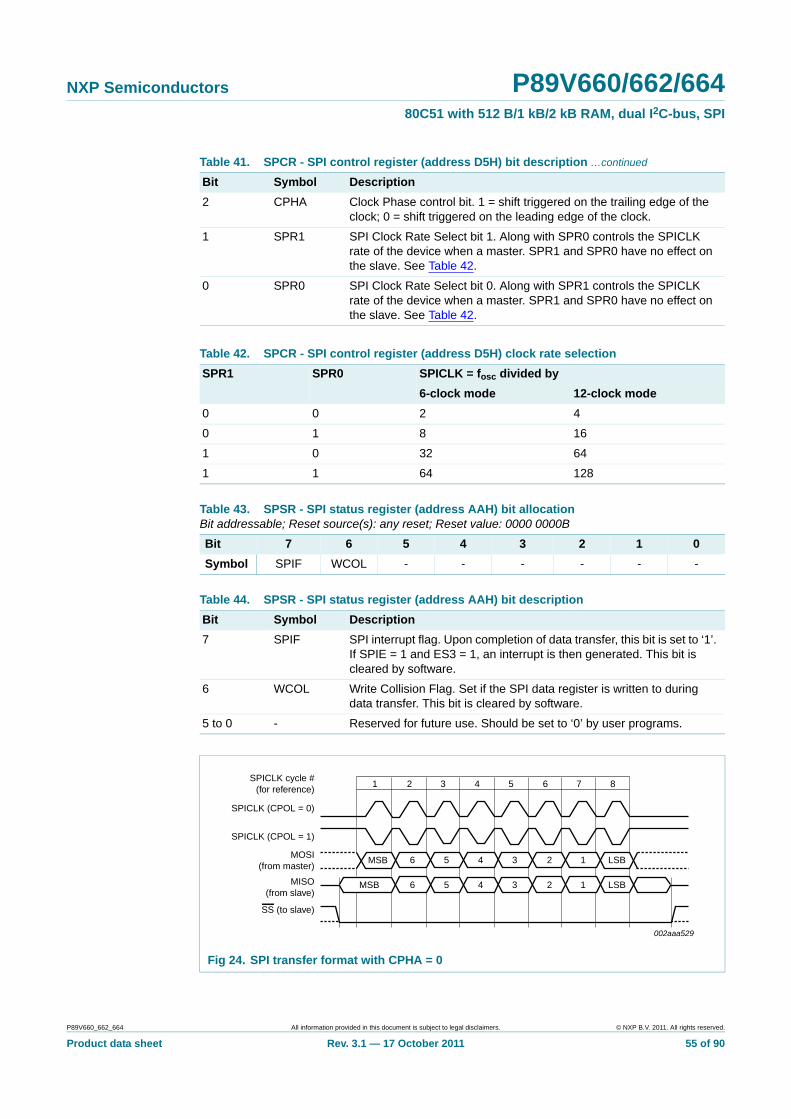
NXP Semiconductors P89V660/662/66480C51 with 512 B/1 kB/2 kB RAM, dual I2C-bus, SPI
2 CPHA Clock Phase control bit. 1 = shift triggered on the trailing edge of the clock; 0 = shift triggered on the leading edge of the clock.
1 SPR1 SPI Clock Rate Select bit 1. Along with SPR0 controls the SPICLK rate of the device when a master. SPR1 and SPR0 have no effect on the slave. See Table 42.
0 SPR0 SPI Clock Rate Select bit 0. Along with SPR1 controls the SPICLK rate of the device when a master. SPR1 and SPR0 have no effect on the slave. See Table 42.
Table 42. SPCR - SPI control register (address D5H) clock rate selection
SPR1 SPR0 SPICLK = fosc divided by
6-clock mode 12-clock mode
0 0 2 4
0 1 8 16
1 0 32 64
1 1 64 128
Table 43. SPSR - SPI status register (address AAH) bit allocationBit addressable; Reset source(s): any reset; Reset value: 0000 0000B
Bit 7 6 5 4 3 2 1 0
Symbol SPIF WCOL - - - - - -
Table 44. SPSR - SPI status register (address AAH) bit description
Bit Symbol Description
7 SPIF SPI interrupt flag. Upon completion of data transfer, this bit is set to ‘1’. If SPIE = 1 and ES3 = 1, an interrupt is then generated. This bit is cleared by software.
6 WCOL Write Collision Flag. Set if the SPI data register is written to during data transfer. This bit is cleared by software.
5 to 0 - Reserved for future use. Should be set to ‘0’ by user programs.
Fig 24. SPI transfer format with CPHA = 0
Table 41. SPCR - SPI control register (address D5H) bit description …continued
Bit Symbol Description
002aaa529
SPICLK cycle #(for reference)
SPICLK (CPOL = 0)
SPICLK (CPOL = 1)
MOSI(from master)
MISO(from slave)
SS (to slave)
1 2 3 4 5 6 7 8
MSB 6 5 4 3 2 1 LSB
MSB 6 5 4 3 2 1 LSB
P89V660_662_664 All information provided in this document is subject to legal disclaimers. © NXP B.V. 2011. All rights reserved.
Product data sheet Rev. 3.1 — 17 October 2011 55 of 90

NXP Semiconductors P89V660/662/66480C51 with 512 B/1 kB/2 kB RAM, dual I2C-bus, SPI
6.9 Watchdog timer
The WDT is intended as a recovery method in situations where the CPU may be subjected to software upset. The WDT consists of a 14-bit counter and the WatchDog Timer Reset (WDTRST) SFR. The WDT is disabled at reset. To enable the WDT, the user must write 01EH and 0E1H, in sequence, to the WDTRST SFR. When the WDT is enabled, it will increment every machine cycle while the oscillator is running and there is no way to disable the WDT, except through a reset (either hardware reset or a WDT overflow reset). When the WDT overflows, it will drive an output reset HIGH pulse at the RST pin.
When the WDT is enabled (and thus running) the user needs to reset it by writing 01EH and 0E1H, in sequence, to the WDTRST SFR to avoid WDT overflow. The 14-bit counter reaches overflow when it reaches 16383 (3FFFH) and this will reset the device.
The WDT’s counter cannot be read or written. When the WDT overflows it will generate a output pulse at the reset pin with a duration of 98 oscillator periods in 6 clock mode or 196 oscillator periods in 12 clock mode.
6.10 PCA
The PCA includes a special 16-bit Timer that has five 16-bit capture/compare modules associated with it. Each of the modules can be programmed to operate in one of four modes: rising and/or falling edge capture, software timer, high-speed output, or pulse width modulator. Each module has a pin associated with it. Module 0 is connected to CEX0, module 1 to CEX1, etc. Registers CH and CL contain current value of the free running up counting 16-bit PCA timer. The PCA timer is a common time base for all five modules and can be programmed to run at: 1⁄6 the oscillator frequency, 1⁄2 the oscillator frequency, the Timer 0 overflow, or the input on the ECI pin (P1[2]). The timer count source is determined from the CPS1 and CPS0 bits in the CMOD SFR (see Table 45 and Table 46).
Fig 25. SPI transfer format with CPHA = 1
002aaa530
MSB
SPICLK cycle #(for reference)
SPICLK (CPOL = 0)
SPICLK (CPOL = 1)
MOSI(from master)
MISO(from slave)
SS (to slave)
6
1 2 3 4 5 6 7 8
5
MSB 6 5 4 3 2 1 LSB
4 3 2 1 LSB
P89V660_662_664 All information provided in this document is subject to legal disclaimers. © NXP B.V. 2011. All rights reserved.
Product data sheet Rev. 3.1 — 17 October 2011 56 of 90

NXP Semiconductors P89V660/662/66480C51 with 512 B/1 kB/2 kB RAM, dual I2C-bus, SPI
In the CMOD SFR there are three additional bits associated with the PCA. They are CIDL which allows the PCA to stop during Idle mode, WDTE which enables or disables the Watchdog function on module 4, and ECF which when set causes an interrupt and the PCA overflow flag CF (in the CCON SFR) to be set when the PCA timer overflows.
The watchdog timer function is implemented in module 4 of PCA.
The CCON SFR contains the run control bit for the PCA (CR) and the flags for the PCA timer (CF) and each module (CCF4:0). To run the PCA the CR bit (CCON.6) must be set by software. The PCA is shut off by clearing this bit. The CF bit (CCON.7) is set when the PCA counter overflows and an interrupt will be generated if the ECF bit in the CMOD register is set. The CF bit can only be cleared by software. Bits 0 through 4 of the CCON register are the flags for the modules (bit 0 for module 0, bit 1 for module 1, etc.) and are set by hardware when either a match or a capture occurs. These flags can only be cleared by software. All the modules share one interrupt vector. The PCA interrupt system is shown in Figure 27.
Each module in the PCA has a special function register associated with it. These registers are: CCAPM0 for module 0, CCAPM1 for module 1, etc. The registers contain the bits that control the mode that each module will operate in.
The ECCF bit (from CCAPMn.0 where n = 0, 1, 2, 3, or 4 depending on the module) enables the CCFn flag in the CCON SFR to generate an interrupt when a match or compare occurs in the associated module (see Figure 27).
PWM (CCAPMn.1) enables the pulse width modulation mode.
The TOG bit (CCAPMn.2) when set causes the CEX output associated with the module to toggle when there is a match between the PCA counter and the module’s capture/compare register.
The match bit MAT (CCAPMn.3) when set will cause the CCFn bit in the CCON register to be set when there is a match between the PCA counter and the module’s capture/compare register.
Fig 26. PCA
MODULE0
PCA TIMER/COUNTER
P1[3]/CEX0
MODULE1 P1[4]/CEX1
MODULE2 P1[5]/CEX2
MODULE3 P1[6]/CEX3
MODULE4 P1[7]/CEX4
time base for PCA modules
Module functions:- 16-bit capture- 16-bit timer- 16-bit high speed output- 8-bit PWM- watchdog timer (module 4 only)
16 bits
16 bits
002aab913
P89V660_662_664 All information provided in this document is subject to legal disclaimers. © NXP B.V. 2011. All rights reserved.
Product data sheet Rev. 3.1 — 17 October 2011 57 of 90

NXP Semiconductors P89V660/662/66480C51 with 512 B/1 kB/2 kB RAM, dual I2C-bus, SPI
The next two bits CAPN (CCAPMn.4) and CAPP (CCAPMn.5) determine the edge that a capture input will be active on. The CAPN bit enables the negative edge, and the CAPP bit enables the positive edge. If both bits are set both edges will be enabled and a capture will occur for either transition.
The last bit in the register ECOM (CCAPMn.6) when set enables the comparator function.
There are two additional registers associated with each of the PCA modules. They are CCAPnH and CCAPnL and these are the registers that store the 16-bit count when a capture occurs or a compare should occur. When a module is used in the PWM mode these registers are used to control the duty cycle of the output.
Fig 27. PCA interrupt system
002aab914
PCA TIMER/COUNTER
MODULE0
CF CR - CCF4 CCF3 CCF2 CCF1 CCF0
MODULE1
MODULE2
MODULE3
MODULE4
ECF ECCFn
IEN0.6EC
IEN0.7EA
CCAPMn.0CMOD.0
CCON(C0h)
tointerruptprioritydecoder
Table 45. CMOD - PCA counter mode register (address C1H) bit allocationNot bit addressable; Reset value: 00H
Bit 7 6 5 4 3 2 1 0
Symbol CIDL WDTE - - - CPS1 CPS0 ECF
P89V660_662_664 All information provided in this document is subject to legal disclaimers. © NXP B.V. 2011. All rights reserved.
Product data sheet Rev. 3.1 — 17 October 2011 58 of 90
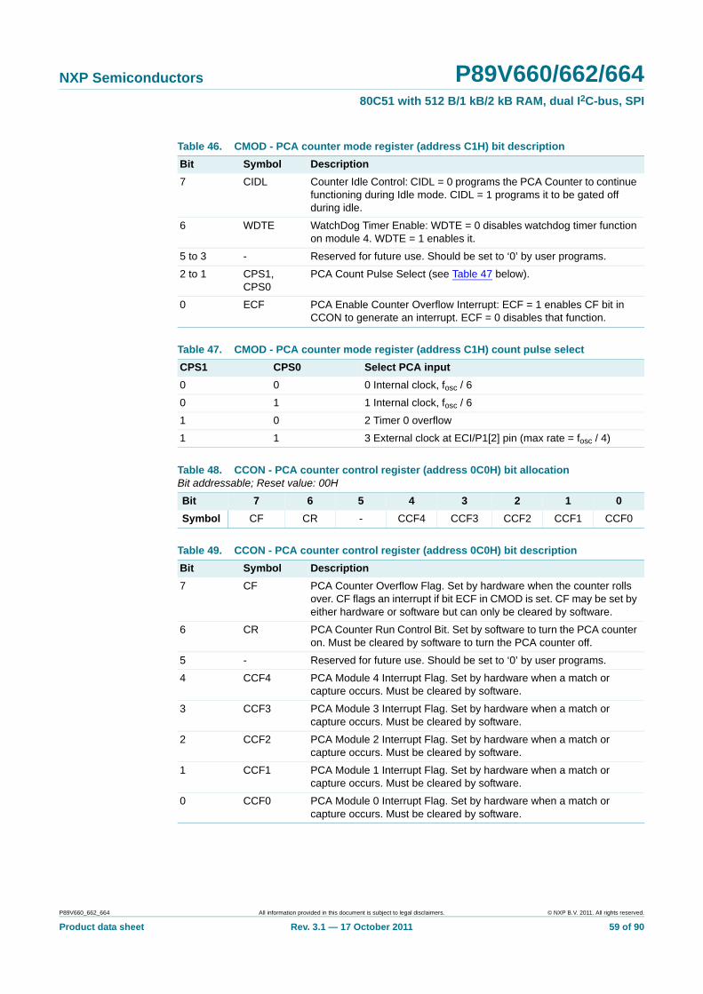
NXP Semiconductors P89V660/662/66480C51 with 512 B/1 kB/2 kB RAM, dual I2C-bus, SPI
Table 46. CMOD - PCA counter mode register (address C1H) bit description
Bit Symbol Description
7 CIDL Counter Idle Control: CIDL = 0 programs the PCA Counter to continue functioning during Idle mode. CIDL = 1 programs it to be gated off during idle.
6 WDTE WatchDog Timer Enable: WDTE = 0 disables watchdog timer function on module 4. WDTE = 1 enables it.
5 to 3 - Reserved for future use. Should be set to ‘0’ by user programs.
2 to 1 CPS1, CPS0
PCA Count Pulse Select (see Table 47 below).
0 ECF PCA Enable Counter Overflow Interrupt: ECF = 1 enables CF bit in CCON to generate an interrupt. ECF = 0 disables that function.
Table 47. CMOD - PCA counter mode register (address C1H) count pulse select
CPS1 CPS0 Select PCA input
0 0 0 Internal clock, fosc / 6
0 1 1 Internal clock, fosc / 6
1 0 2 Timer 0 overflow
1 1 3 External clock at ECI/P1[2] pin (max rate = fosc / 4)
Table 48. CCON - PCA counter control register (address 0C0H) bit allocationBit addressable; Reset value: 00H
Bit 7 6 5 4 3 2 1 0
Symbol CF CR - CCF4 CCF3 CCF2 CCF1 CCF0
Table 49. CCON - PCA counter control register (address 0C0H) bit description
Bit Symbol Description
7 CF PCA Counter Overflow Flag. Set by hardware when the counter rolls over. CF flags an interrupt if bit ECF in CMOD is set. CF may be set by either hardware or software but can only be cleared by software.
6 CR PCA Counter Run Control Bit. Set by software to turn the PCA counter on. Must be cleared by software to turn the PCA counter off.
5 - Reserved for future use. Should be set to ‘0’ by user programs.
4 CCF4 PCA Module 4 Interrupt Flag. Set by hardware when a match or capture occurs. Must be cleared by software.
3 CCF3 PCA Module 3 Interrupt Flag. Set by hardware when a match or capture occurs. Must be cleared by software.
2 CCF2 PCA Module 2 Interrupt Flag. Set by hardware when a match or capture occurs. Must be cleared by software.
1 CCF1 PCA Module 1 Interrupt Flag. Set by hardware when a match or capture occurs. Must be cleared by software.
0 CCF0 PCA Module 0 Interrupt Flag. Set by hardware when a match or capture occurs. Must be cleared by software.
P89V660_662_664 All information provided in this document is subject to legal disclaimers. © NXP B.V. 2011. All rights reserved.
Product data sheet Rev. 3.1 — 17 October 2011 59 of 90

NXP Semiconductors P89V660/662/66480C51 with 512 B/1 kB/2 kB RAM, dual I2C-bus, SPI
6.10.1 PCA capture mode
To use one of the PCA modules in the capture mode (Figure 28) either one or both of the CCAPM bits CAPN and CAPP for that module must be set. The external CEX input for the module (on port 1) is sampled for a transition. When a valid transition occurs the PCA hardware loads the value of the PCA counter registers (CH and CL) into the module’s capture registers (CCAPnL and CCAPnH).
Table 50. CCAPMn - PCA modules compare/capture register (address CCAPM0 0C2H, CCAPM1 0C3H, CCAPM2 0C4H, CCAPM3 0C5H, CCAPM4 0C6H) bit allocation
Not bit addressable; Reset value: 00H
Bit 7 6 5 4 3 2 1 0
Symbol - ECOMn CAPPn CAPNn MATn TOGn PWMn ECCFn
Table 51. CCAPMn - PCA modules compare/capture register (address CCAPM0 0C2H, CCAPM1 0C3H, CCAPM2 0C4H, CCAPM3 0C5H, CCAPM4 0C6H) bit description
Bit Symbol Description
7 - Reserved for future use. Should be set to ‘0’ by user programs.
6 ECOMn Enable Comparator. ECOMn = 1 enables the comparator function.
5 CAPPn Capture Positive, CAPPn = 1 enables positive edge capture.
4 CAPNn Capture Negative, CAPNn = 1 enables negative edge capture.
3 MATn Match. When MATn = 1 a match of the PCA counter with this module’s compare/capture register causes the CCFn bit in CCON to be set, flagging an interrupt.
2 TOGn Toggle. When TOGn = 1, a match of the PCA counter with this module’s compare/capture register causes the CEXn pin to toggle.
1 PWMn Pulse Width Modulation mode. PWMn = 1 enables the CEXn pin to be used as a pulse width modulated output.
0 ECCFn Enable CCF Interrupt. Enables compare/capture flag CCFn in the CCON register to generate an interrupt.
Table 52. PCA module modes (CCAPMn register)
ECOMn CAPPn CAPNn MATn TOGn PWMn ECCFn Module function
0 0 0 0 0 0 0 no operation
x 1 0 0 0 0 x 16-bit capture by a positive-edge trigger on CEXn
x 0 1 0 0 0 x 16-bit capture by a negative-edge trigger on CEXn
x 1 1 0 0 0 x 16-bit capture by any transition on CEXn
1 0 0 1 0 0 x 16-bit software timer
1 0 0 1 1 0 x 16-bit high-speed output
1 0 0 0 0 1 0 8-bit PWM
1 0 0 1 x 0 x watchdog timer
P89V660_662_664 All information provided in this document is subject to legal disclaimers. © NXP B.V. 2011. All rights reserved.
Product data sheet Rev. 3.1 — 17 October 2011 60 of 90
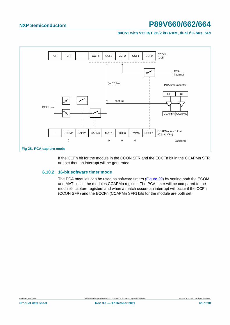
NXP Semiconductors P89V660/662/66480C51 with 512 B/1 kB/2 kB RAM, dual I2C-bus, SPI
If the CCFn bit for the module in the CCON SFR and the ECCFn bit in the CCAPMn SFR are set then an interrupt will be generated.
6.10.2 16-bit software timer mode
The PCA modules can be used as software timers (Figure 29) by setting both the ECOM and MAT bits in the modules CCAPMn register. The PCA timer will be compared to the module’s capture registers and when a match occurs an interrupt will occur if the CCFn (CCON SFR) and the ECCFn (CCAPMn SFR) bits for the module are both set.
Fig 28. PCA capture mode
002aab915
CF CR - CCF4 CCF3 CCF2 CCF1 CCF0 CCON(C0h)
PCAinterrupt
PCA timer/counter
- ECOMn
0 0 0 0
CAPPn CAPNn MATn TOGn PWMn ECCFnCCAPMn, n = 0 to 4(C2h to C6h)
CH CL
CCAPnH CCAPnL
capture
(to CCFn)
CEXn
P89V660_662_664 All information provided in this document is subject to legal disclaimers. © NXP B.V. 2011. All rights reserved.
Product data sheet Rev. 3.1 — 17 October 2011 61 of 90
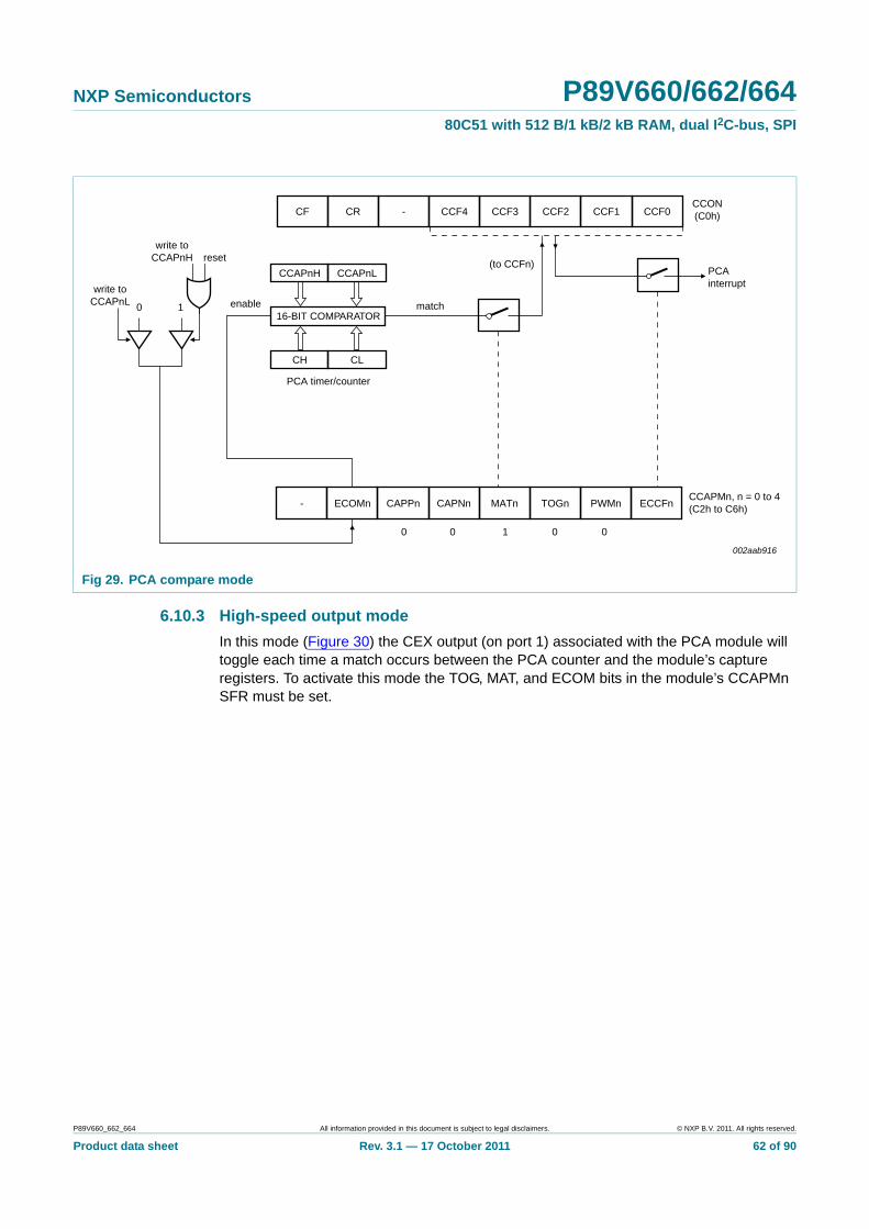
NXP Semiconductors P89V660/662/66480C51 with 512 B/1 kB/2 kB RAM, dual I2C-bus, SPI
6.10.3 High-speed output mode
In this mode (Figure 30) the CEX output (on port 1) associated with the PCA module will toggle each time a match occurs between the PCA counter and the module’s capture registers. To activate this mode the TOG, MAT, and ECOM bits in the module’s CCAPMn SFR must be set.
Fig 29. PCA compare mode
002aab916
CF CR - CCF4 CCF3 CCF2 CCF1 CCF0CCON(C0h)
PCAinterrupt
- ECOMn
0 0 1 0 0
CAPPn CAPNn MATn TOGn PWMn ECCFnCCAPMn, n = 0 to 4(C2h to C6h)
16-BIT COMPARATOR
PCA timer/counter
CH CL
match
(to CCFn)CCAPnH CCAPnL
enable
write toCCAPnH
write toCCAPnL
reset
0 1
P89V660_662_664 All information provided in this document is subject to legal disclaimers. © NXP B.V. 2011. All rights reserved.
Product data sheet Rev. 3.1 — 17 October 2011 62 of 90
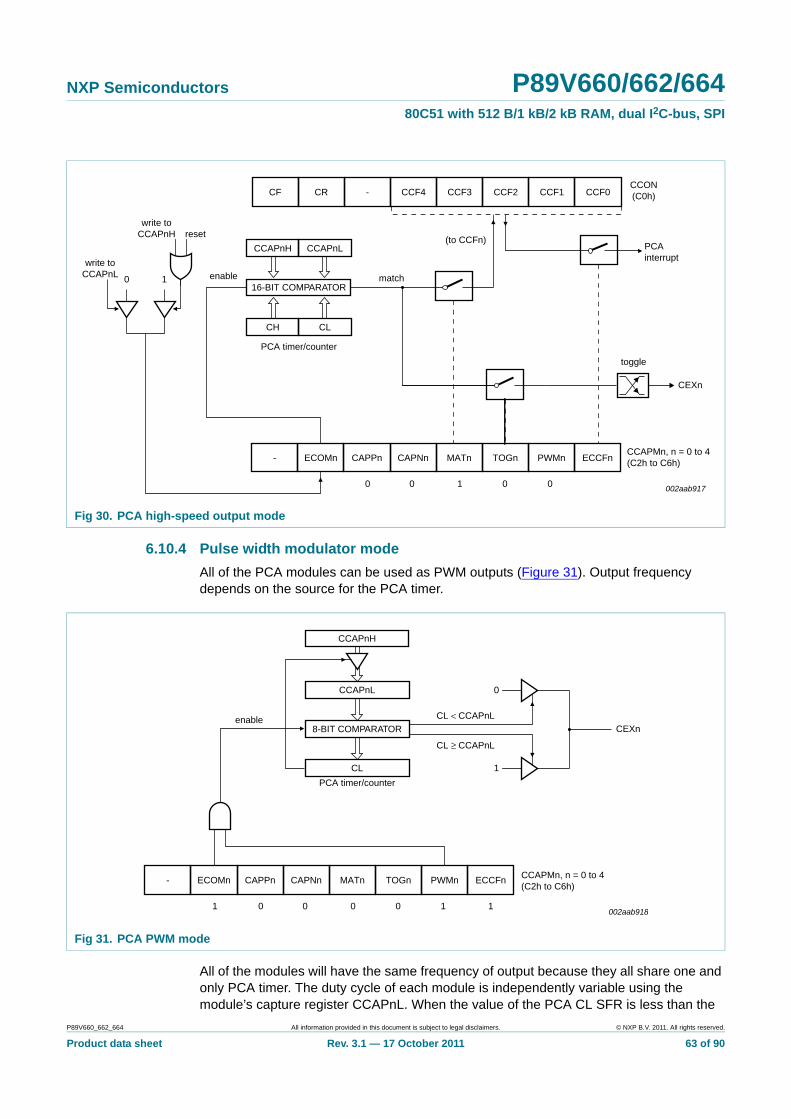
NXP Semiconductors P89V660/662/66480C51 with 512 B/1 kB/2 kB RAM, dual I2C-bus, SPI
6.10.4 Pulse width modulator mode
All of the PCA modules can be used as PWM outputs (Figure 31). Output frequency depends on the source for the PCA timer.
All of the modules will have the same frequency of output because they all share one and only PCA timer. The duty cycle of each module is independently variable using the module’s capture register CCAPnL. When the value of the PCA CL SFR is less than the
Fig 30. PCA high-speed output mode
002aab917
toggle
CEXn
CF CR - CCF4 CCF3 CCF2 CCF1 CCF0CCON(C0h)
PCAinterrupt
- ECOMn
0 0 1 0 0
CAPPn CAPNn MATn TOGn PWMn ECCFnCCAPMn, n = 0 to 4(C2h to C6h)
16-BIT COMPARATOR
PCA timer/counter
CH CL
match
(to CCFn)CCAPnH CCAPnL
enable
write toCCAPnH
write toCCAPnL
reset
0 1
Fig 31. PCA PWM mode
002aab918
- ECOMn
01 0 0 0 1 1
CAPPn CAPNn MATn TOGn PWMn ECCFn CCAPMn, n = 0 to 4(C2h to C6h)
CCAPnL
8-BIT COMPARATOR
PCA timer/counter
CCAPnH
CL
enableCEXn
CL < CCAPnL
CL ≥ CCAPnL
0
1
P89V660_662_664 All information provided in this document is subject to legal disclaimers. © NXP B.V. 2011. All rights reserved.
Product data sheet Rev. 3.1 — 17 October 2011 63 of 90

NXP Semiconductors P89V660/662/66480C51 with 512 B/1 kB/2 kB RAM, dual I2C-bus, SPI
value in the module’s CCAPnL SFR the output will be low, when it is equal to or greater than the output will be high. When CL overflows from FF to 00, CCAPnL is reloaded with the value in CCAPnH. This allows updating the PWM without glitches. The PWM and ECOM bits in the module’s CCAPMn register must be set to enable the PWM mode.
6.10.5 PCA watchdog timer
An on-board watchdog timer is available with the PCA to improve the reliability of the system without increasing chip count. Watchdog timers are useful for systems that are susceptible to noise, power glitches, or electrostatic discharge. Module 4 is the only PCA module that can be programmed as a Watchdog. However, this module can still be used for other modes if the Watchdog is not needed. Figure 31 shows a diagram of how the Watchdog works. The user pre-loads a 16-bit value in the compare registers. Just like the other compare modes, this 16-bit value is compared to the PCA timer value. If a match is allowed to occur, an internal reset will be generated. This will not cause the RST pin to be driven high.
user’s software then must periodically change (CCAP4H,CCAP4L) to keep a match from occurring with the PCA timer (CH,CL). This code is given in the WATCHDOG routine shown above.
In order to hold off the reset, the user has three options:
1. Periodically change the compare value so it will never match the PCA timer.
2. Periodically change the PCA timer value so it will never match the compare values.
3. Disable the Watchdog by clearing the WDTE bit before a match occurs and then re-enable it.
The first two options are more reliable because the watchdog timer is never disabled as in option #3. If the program counter ever goes astray, a match will eventually occur and cause an internal reset. The second option is also not recommended if other PCA modules are being used. Remember, the PCA timer is the time base for all modules; changing the time base for other modules would not be a good idea. Thus, in most applications the first solution is the best option.
;CALL the following WATCHDOG subroutine periodically.CLR EA ;Hold off interruptsMOV CCAP4L,#00 ;Next compare value is within 255 counts of
current PCA timer valueMOV CCAP4H,CHSETB EA ;Re-enable interruptsRET
This routine should not be part of an interrupt service routine, because if the program counter goes astray and gets stuck in an infinite loop, interrupts will still be serviced and the Watchdog will keep getting reset. Thus, the purpose of the Watchdog would be defeated. Instead, call this subroutine from the main program within 216 count of the PCA timer.
P89V660_662_664 All information provided in this document is subject to legal disclaimers. © NXP B.V. 2011. All rights reserved.
Product data sheet Rev. 3.1 — 17 October 2011 64 of 90

NXP Semiconductors P89V660/662/66480C51 with 512 B/1 kB/2 kB RAM, dual I2C-bus, SPI
6.11 Security bits
The security bits protects against software piracy and prevents the contents of the flash from being read by unauthorized parties in Parallel Programmer mode and ISP mode. Since the end application might need to erase pages and read from the code memory, the security bits have no effect in IAP mode. However, the security bits’ programmed/erased state may be read using IAP function calls allowing the end user code to limit access, if desired. The security bits and their effects are shown in Table 53.
Note: On this device MOVC instructions executed from external code memory are disabled from fetching code bytes from internal code memory.
6.12 Interrupt priority and polling sequence
The device supports eight interrupt sources under a four level priority scheme. Table 54 summarizes the polling sequence of the supported interrupts. Note that the SPI serial interface and the UART share the same interrupt vector. (See Figure 32).
Table 53. Security bit functions
Security bit Description
1 Write protect. When programmed, prohibits further erasing or programming, except to program other security bits or a chip erase.
2 Read protect. When programmed inhibits reading of user code memory.
3 External execution inhibit. When programmed prevents any execution of instructions from external code memory.
Table 54. Interrupt polling sequence
Description Interrupt flag Vector address Interrupt enable
Interrupt priority
Servicepriority
Wake-up Power-down
External Interrupt 0
IE0 0003H EX0 PX0/H 1 (highest) yes
T0 TF0 000BH ET0 PT0/H 3 no
External Interrupt 1
IE1 0013H EX1 PX1/H 4 yes
T1 TF1 001BH ET1 PT1/H 5 no
UART TI/RI 0023H ES0 PS0/H 6 no
I2C-bus (primary)
- 002BH ES1 PS1/H 2 no
PCA CF/CCFn 0033H EC PPCH 8 no
T2 TF2, EXF2 003BH ET2 PT2/H 7 no
I2C-bus (secondary)
- 0043H ES2 PS2/H 10 no
SPI SPIF 004BH ES3 PS3/H 9 no
P89V660_662_664 All information provided in this document is subject to legal disclaimers. © NXP B.V. 2011. All rights reserved.
Product data sheet Rev. 3.1 — 17 October 2011 65 of 90
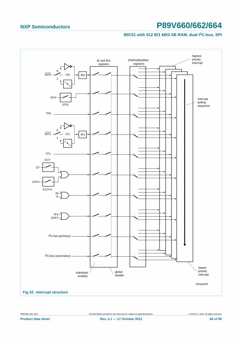
NXP Semiconductors P89V660/662/66480C51 with 512 B/1 kB/2 kB RAM, dual I2C-bus, SPI
Fig 32. Interrupt structure
002aab919
highestpriorityinterrupt
interruptpollingsequence
INT0
IE and IEAregisters
IP/IPH/IPA/IPAH registers
individualenables
globaldisable
IE0
0
1IT0
lowestpriorityinterrupt
SPIE
SPIF
TF0
INT1
TF1
CF
ECF
CCFn
ECCFnRITI
TF2EXF2
I2C-bus (primary)
I2C-bus (secondary)
IE1
0
1IT1
P89V660_662_664 All information provided in this document is subject to legal disclaimers. © NXP B.V. 2011. All rights reserved.
Product data sheet Rev. 3.1 — 17 October 2011 66 of 90
NXP Semiconductors P89V660/662/66480C51 with 512 B/1 kB/2 kB RAM, dual I2C-bus, SPI
Table 55. IEN0 - Interrupt enable register 0 (address A8H) bit allocationBit addressable; Reset value: 00H
Bit 7 6 5 4 3 2 1 0
Symbol EA EC ES1 ES0 ET1 EX1 ET0 EX0
Table 56. IEN0 - Interrupt enable register 0 (address A8H) bit description
Bit Symbol Description
7 EA Interrupt Enable Bit: EA = 1 interrupt(s) can be serviced, EA = 0 interrupt servicing disabled.
6 EC PCA Interrupt Enable bit.
5 ES1 I2C-bus Interrupt Enable (primary).
4 ES0 Serial Port Interrupt Enable
3 ET1 Timer 1 Overflow Interrupt Enable.
2 EX1 External Interrupt 1 Enable.
1 ET0 Timer 0 Overflow Interrupt Enable.
0 EX0 External Interrupt 0 Enable.
Table 57. IEN1 - Interrupt enable register 1 (address E8H) bit allocationBit addressable; Reset value: 00H
Bit 7 6 5 4 3 2 1 0
Symbol - - - - - ES3 ES2 ET2
Table 58. IEN1 - Interrupt enable register 1 (address E8H) bit description
Bit Symbol Description
7 to 3 - Reserved for future use. Should be set to ‘0’ by user programs.
2 ES3 SPI Interrupt Enable.
1 ES2 I2C-bus Interrupt Enable (secondary).
0 ET2 Timer 2 Interrupt Enable.
Table 59. IP0 - Interrupt priority 0 low register (address B8H) bit allocationBit addressable; Reset value: 00H
Bit 7 6 5 4 3 2 1 0
Symbol PT2 PPC PS1 PS0 PT1 PX1 PT0 PX0
Table 60. IP0 - Interrupt priority 0 low register (address B8H) bit description
Bit Symbol Description
7 PT2 Timer 2 Interrupt Priority Low Bit.
6 PPC PCA Interrupt Priority Low Bit.
5 PS1 I2C-bus Interrupt Priority Low Bit.
4 PS0 Serial Port Interrupt Priority Low Bit.
3 PT1 Timer 1 Interrupt Priority Low Bit.
2 PX1 External Interrupt 1 Priority Low Bit.
1 PT0 Timer 0 Interrupt Priority Low Bit.
0 PX0 External Interrupt 0 Priority Low Bit.
P89V660_662_664 All information provided in this document is subject to legal disclaimers. © NXP B.V. 2011. All rights reserved.
Product data sheet Rev. 3.1 — 17 October 2011 67 of 90
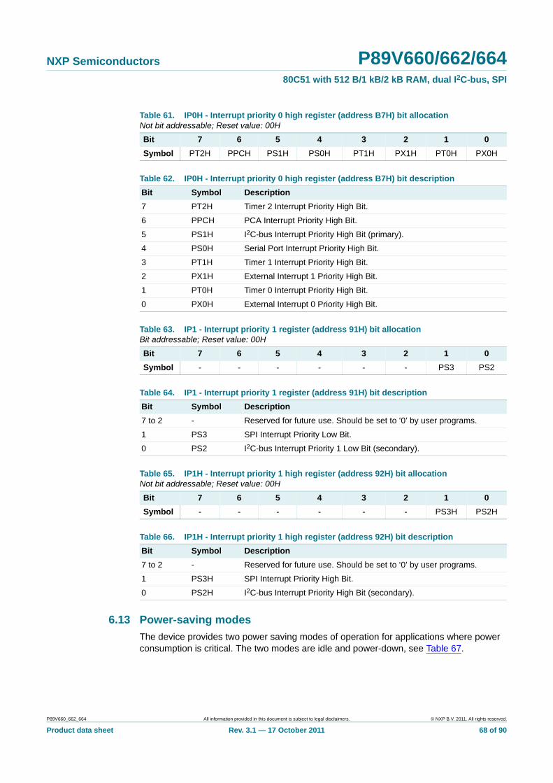
NXP Semiconductors P89V660/662/66480C51 with 512 B/1 kB/2 kB RAM, dual I2C-bus, SPI
6.13 Power-saving modes
The device provides two power saving modes of operation for applications where power consumption is critical. The two modes are idle and power-down, see Table 67.
Table 61. IP0H - Interrupt priority 0 high register (address B7H) bit allocationNot bit addressable; Reset value: 00H
Bit 7 6 5 4 3 2 1 0
Symbol PT2H PPCH PS1H PS0H PT1H PX1H PT0H PX0H
Table 62. IP0H - Interrupt priority 0 high register (address B7H) bit description
Bit Symbol Description
7 PT2H Timer 2 Interrupt Priority High Bit.
6 PPCH PCA Interrupt Priority High Bit.
5 PS1H I2C-bus Interrupt Priority High Bit (primary).
4 PS0H Serial Port Interrupt Priority High Bit.
3 PT1H Timer 1 Interrupt Priority High Bit.
2 PX1H External Interrupt 1 Priority High Bit.
1 PT0H Timer 0 Interrupt Priority High Bit.
0 PX0H External Interrupt 0 Priority High Bit.
Table 63. IP1 - Interrupt priority 1 register (address 91H) bit allocationBit addressable; Reset value: 00H
Bit 7 6 5 4 3 2 1 0
Symbol - - - - - - PS3 PS2
Table 64. IP1 - Interrupt priority 1 register (address 91H) bit description
Bit Symbol Description
7 to 2 - Reserved for future use. Should be set to ‘0’ by user programs.
1 PS3 SPI Interrupt Priority Low Bit.
0 PS2 I2C-bus Interrupt Priority 1 Low Bit (secondary).
Table 65. IP1H - Interrupt priority 1 high register (address 92H) bit allocationNot bit addressable; Reset value: 00H
Bit 7 6 5 4 3 2 1 0
Symbol - - - - - - PS3H PS2H
Table 66. IP1H - Interrupt priority 1 high register (address 92H) bit description
Bit Symbol Description
7 to 2 - Reserved for future use. Should be set to ‘0’ by user programs.
1 PS3H SPI Interrupt Priority High Bit.
0 PS2H I2C-bus Interrupt Priority High Bit (secondary).
P89V660_662_664 All information provided in this document is subject to legal disclaimers. © NXP B.V. 2011. All rights reserved.
Product data sheet Rev. 3.1 — 17 October 2011 68 of 90
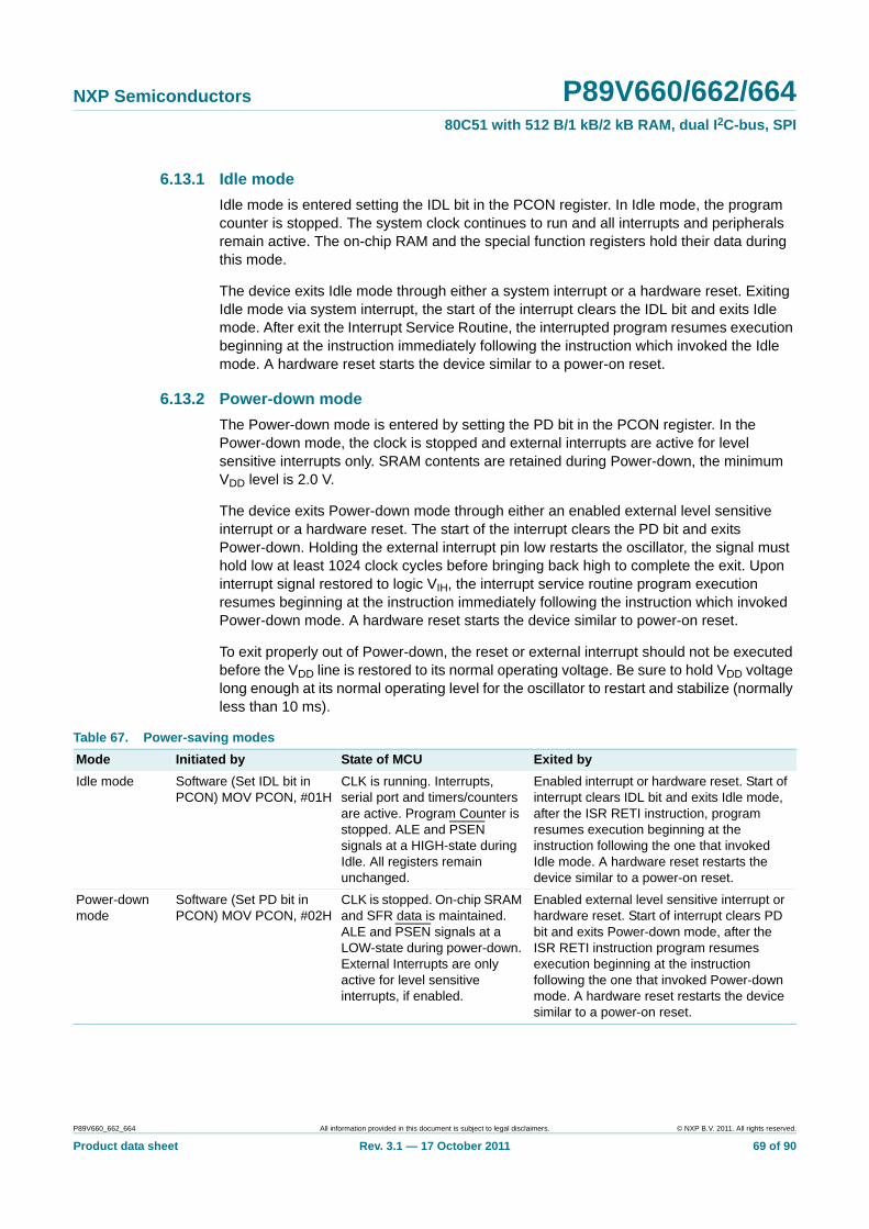
NXP Semiconductors P89V660/662/66480C51 with 512 B/1 kB/2 kB RAM, dual I2C-bus, SPI
6.13.1 Idle mode
Idle mode is entered setting the IDL bit in the PCON register. In Idle mode, the program counter is stopped. The system clock continues to run and all interrupts and peripherals remain active. The on-chip RAM and the special function registers hold their data during this mode.
The device exits Idle mode through either a system interrupt or a hardware reset. Exiting Idle mode via system interrupt, the start of the interrupt clears the IDL bit and exits Idle mode. After exit the Interrupt Service Routine, the interrupted program resumes execution beginning at the instruction immediately following the instruction which invoked the Idle mode. A hardware reset starts the device similar to a power-on reset.
6.13.2 Power-down mode
The Power-down mode is entered by setting the PD bit in the PCON register. In the Power-down mode, the clock is stopped and external interrupts are active for level sensitive interrupts only. SRAM contents are retained during Power-down, the minimum VDD level is 2.0 V.
The device exits Power-down mode through either an enabled external level sensitive interrupt or a hardware reset. The start of the interrupt clears the PD bit and exits Power-down. Holding the external interrupt pin low restarts the oscillator, the signal must hold low at least 1024 clock cycles before bringing back high to complete the exit. Upon interrupt signal restored to logic VIH, the interrupt service routine program execution resumes beginning at the instruction immediately following the instruction which invoked Power-down mode. A hardware reset starts the device similar to power-on reset.
To exit properly out of Power-down, the reset or external interrupt should not be executed before the VDD line is restored to its normal operating voltage. Be sure to hold VDD voltage long enough at its normal operating level for the oscillator to restart and stabilize (normally less than 10 ms).
Table 67. Power-saving modes
Mode Initiated by State of MCU Exited by
Idle mode Software (Set IDL bit in PCON) MOV PCON, #01H
CLK is running. Interrupts, serial port and timers/counters are active. Program Counter is stopped. ALE and PSEN signals at a HIGH-state during Idle. All registers remain unchanged.
Enabled interrupt or hardware reset. Start of interrupt clears IDL bit and exits Idle mode, after the ISR RETI instruction, program resumes execution beginning at the instruction following the one that invoked Idle mode. A hardware reset restarts the device similar to a power-on reset.
Power-down mode
Software (Set PD bit in PCON) MOV PCON, #02H
CLK is stopped. On-chip SRAM and SFR data is maintained. ALE and PSEN signals at a LOW-state during power-down. External Interrupts are only active for level sensitive interrupts, if enabled.
Enabled external level sensitive interrupt or hardware reset. Start of interrupt clears PD bit and exits Power-down mode, after the ISR RETI instruction program resumes execution beginning at the instruction following the one that invoked Power-down mode. A hardware reset restarts the device similar to a power-on reset.
P89V660_662_664 All information provided in this document is subject to legal disclaimers. © NXP B.V. 2011. All rights reserved.
Product data sheet Rev. 3.1 — 17 October 2011 69 of 90
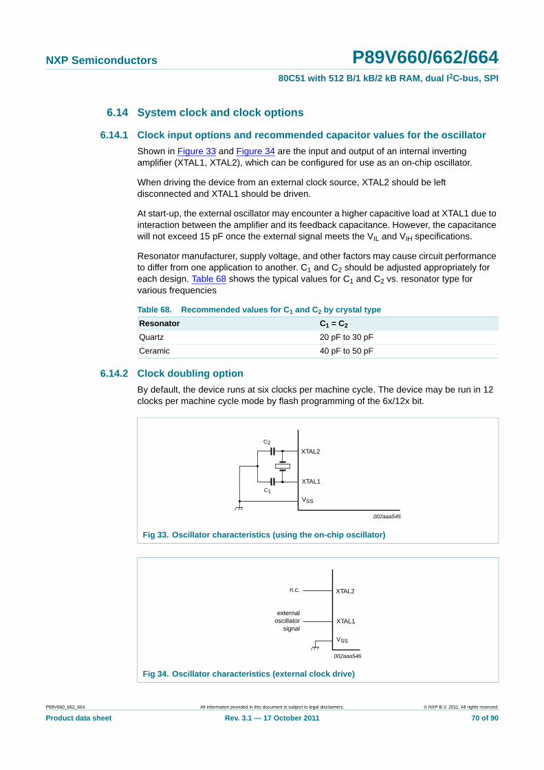
NXP Semiconductors P89V660/662/66480C51 with 512 B/1 kB/2 kB RAM, dual I2C-bus, SPI
6.14 System clock and clock options
6.14.1 Clock input options and recommended capacitor values for the oscillator
Shown in Figure 33 and Figure 34 are the input and output of an internal inverting amplifier (XTAL1, XTAL2), which can be configured for use as an on-chip oscillator.
When driving the device from an external clock source, XTAL2 should be left disconnected and XTAL1 should be driven.
At start-up, the external oscillator may encounter a higher capacitive load at XTAL1 due to interaction between the amplifier and its feedback capacitance. However, the capacitance will not exceed 15 pF once the external signal meets the VIL and VIH specifications.
Resonator manufacturer, supply voltage, and other factors may cause circuit performance to differ from one application to another. C1 and C2 should be adjusted appropriately for each design. Table 68 shows the typical values for C1 and C2 vs. resonator type for various frequencies
6.14.2 Clock doubling option
By default, the device runs at six clocks per machine cycle. The device may be run in 12 clocks per machine cycle mode by flash programming of the 6x/12x bit.
Table 68. Recommended values for C1 and C2 by crystal type
Resonator C1 = C2
Quartz 20 pF to 30 pF
Ceramic 40 pF to 50 pF
Fig 33. Oscillator characteristics (using the on-chip oscillator)
Fig 34. Oscillator characteristics (external clock drive)
002aaa545
XTAL2
XTAL1
VSS
C1
C2
002aaa546
XTAL2n.c.
XTAL1external
oscillatorsignal
VSS
P89V660_662_664 All information provided in this document is subject to legal disclaimers. © NXP B.V. 2011. All rights reserved.
Product data sheet Rev. 3.1 — 17 October 2011 70 of 90
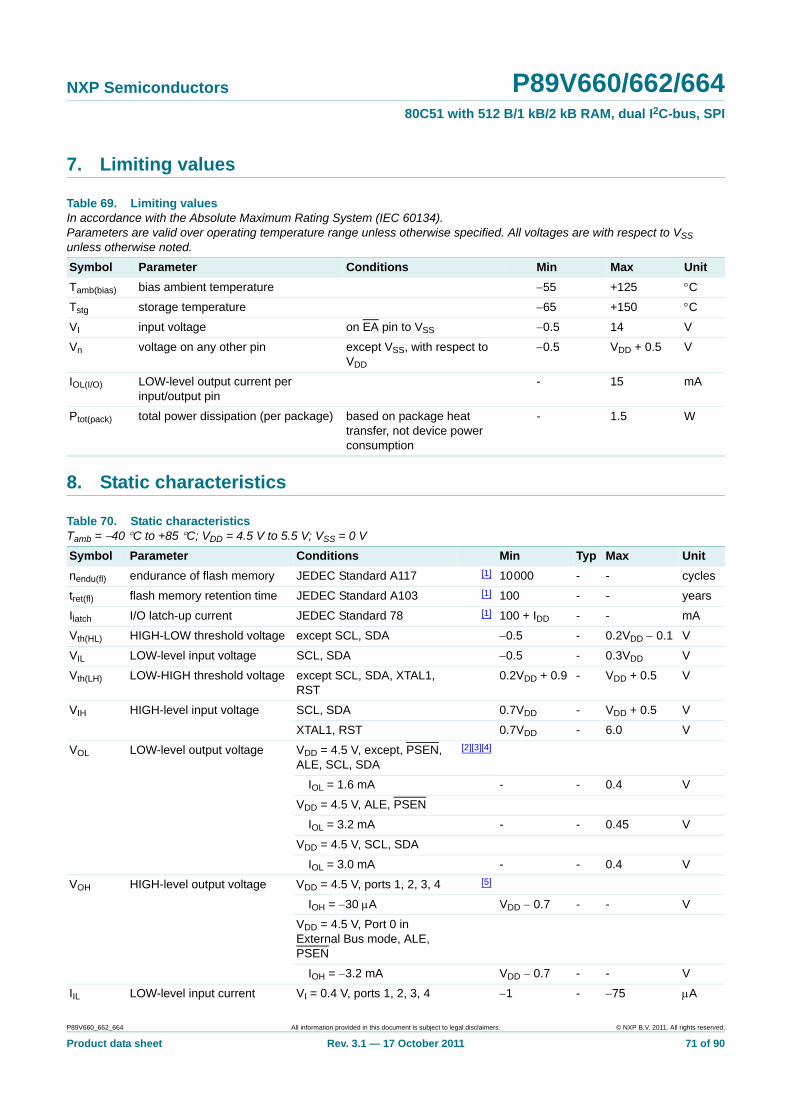
NXP Semiconductors P89V660/662/66480C51 with 512 B/1 kB/2 kB RAM, dual I2C-bus, SPI
7. Limiting values
8. Static characteristics
Table 69. Limiting valuesIn accordance with the Absolute Maximum Rating System (IEC 60134). Parameters are valid over operating temperature range unless otherwise specified. All voltages are with respect to VSS unless otherwise noted.
Symbol Parameter Conditions Min Max Unit
Tamb(bias) bias ambient temperature 55 +125 C
Tstg storage temperature 65 +150 C
VI input voltage on EA pin to VSS 0.5 14 V
Vn voltage on any other pin except VSS, with respect to VDD
0.5 VDD + 0.5 V
IOL(I/O) LOW-level output current per input/output pin
- 15 mA
Ptot(pack) total power dissipation (per package) based on package heat transfer, not device power consumption
- 1.5 W
Table 70. Static characteristicsTamb = 40 C to +85 C; VDD = 4.5 V to 5.5 V; VSS = 0 V
Symbol Parameter Conditions Min Typ Max Unit
nendu(fl) endurance of flash memory JEDEC Standard A117 [1] 10000 - - cycles
tret(fl) flash memory retention time JEDEC Standard A103 [1] 100 - - years
Ilatch I/O latch-up current JEDEC Standard 78 [1] 100 + IDD - - mA
Vth(HL) HIGH-LOW threshold voltage except SCL, SDA 0.5 - 0.2VDD 0.1 V
VIL LOW-level input voltage SCL, SDA 0.5 - 0.3VDD V
Vth(LH) LOW-HIGH threshold voltage except SCL, SDA, XTAL1, RST
0.2VDD + 0.9 - VDD + 0.5 V
VIH HIGH-level input voltage SCL, SDA 0.7VDD - VDD + 0.5 V
XTAL1, RST 0.7VDD - 6.0 V
VOL LOW-level output voltage VDD = 4.5 V, except, PSEN, ALE, SCL, SDA
[2][3][4]
IOL = 1.6 mA - - 0.4 V
VDD = 4.5 V, ALE, PSEN
IOL = 3.2 mA - - 0.45 V
VDD = 4.5 V, SCL, SDA
IOL = 3.0 mA - - 0.4 V
VOH HIGH-level output voltage VDD = 4.5 V, ports 1, 2, 3, 4 [5]
IOH = 30 A VDD 0.7 - - V
VDD = 4.5 V, Port 0 in External Bus mode, ALE, PSEN
IOH = 3.2 mA VDD 0.7 - - V
IIL LOW-level input current VI = 0.4 V, ports 1, 2, 3, 4 1 - 75 A
P89V660_662_664 All information provided in this document is subject to legal disclaimers. © NXP B.V. 2011. All rights reserved.
Product data sheet Rev. 3.1 — 17 October 2011 71 of 90
NXP Semiconductors P89V660/662/66480C51 with 512 B/1 kB/2 kB RAM, dual I2C-bus, SPI
[1] This parameter is measured only for initial qualification and after a design or process change that could affect this parameter.
[2] Under steady state (non-transient) conditions, IOL must be externally limited as follows:
a) Maximum IOL per 8-bit port: 26 mA
b) Maximum IOL total for all outputs: 71 mA
c) If IOL exceeds the test condition, VOH may exceed the related specification. Pins are not guaranteed to sink current greater than the listed test conditions.
[3] Capacitive loading on Ports 0 and 2 may cause spurious noise to be superimposed on the VOL of ALE and Ports 1 and 3. The noise due to external bus capacitance discharging into the Port 0 and 2 pins when the pins make 1-to-0 transitions during bus operations. In the worst cases (capacitive loading > 100 pF), the noise pulse on the ALE pin may exceed 0.8 V. In such cases, it may be desirable to qualify ALE with a Schmitt trigger, or use an address latch with a Schmitt trigger STROBE input.
[4] Load capacitance for Port 0, ALE and PSEN = 100 pF, load capacitance for all other outputs = 80 pF.
[5] Capacitive loading on Ports 0 and 2 may cause the VOH on ALE and PSEN to momentarily fall below the VDD 0.7 specification when the address bits are stabilizing.
[6] Pins of Ports 1, 2 and 3 source a transition current when they are being externally driven from 1 to 0. The transition current reaches its maximum value when VI is approximately 2 V.
[7] Pin capacitance is characterized but not tested. EA = 25 pF (max).
ITHL HIGH-LOW transition current VI = 2 V, ports 1, 2, 3, 4 [6] - - 650 A
ILI input leakage current 0.45 V < VI < VDD 0.3 V, port 0
- - 10 A
0 V < VI < 6 V, 0 V < VDD< 5.5 V, SCL, SDA
- - 10 A
Rpd pull-down resistance on pin RST 40 - 225 k
Ciss input capacitance @ 1 MHz, Tamb = 25 C, VI = 0 V
[7] - - 15 pF
IDD(oper) operating supply current fosc = 12 MHz - - 11.5 mA
fosc = 40 MHz - - 50 mA
Programming and erase mode
- - 70 mA
IDD(idle) Idle mode supply current fosc = 12 MHz - - 8.5 mA
fosc = 40 MHz - - 42 mA
IDD(pd) Power-down mode supply current
minimum VDD = 2 V - - 90 A
Table 70. Static characteristics …continuedTamb = 40 C to +85 C; VDD = 4.5 V to 5.5 V; VSS = 0 V
Symbol Parameter Conditions Min Typ Max Unit
P89V660_662_664 All information provided in this document is subject to legal disclaimers. © NXP B.V. 2011. All rights reserved.
Product data sheet Rev. 3.1 — 17 October 2011 72 of 90

NXP Semiconductors P89V660/662/66480C51 with 512 B/1 kB/2 kB RAM, dual I2C-bus, SPI
(1) Maximum active IDD
(2) Maximum idle IDD
(3) Typical active IDD
(4) Typical idle IDD
Fig 35. IDD vs. frequency
internal clock frequency (MHz)0 40302010
002aaa813
20
30
10
40
50
IDD(mA)
0
(1)
(2)
(3)
(4)
P89V660_662_664 All information provided in this document is subject to legal disclaimers. © NXP B.V. 2011. All rights reserved.
Product data sheet Rev. 3.1 — 17 October 2011 73 of 90
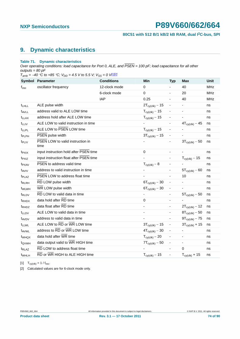
NXP Semiconductors P89V660/662/66480C51 with 512 B/1 kB/2 kB RAM, dual I2C-bus, SPI
9. Dynamic characteristics
[1] Tcy(clk) = 1 / fosc.
[2] Calculated values are for 6-clock mode only.
Table 71. Dynamic characteristicsOver operating conditions: load capacitance for Port 0, ALE, and PSEN = 100 pF; load capacitance for all other outputs = 80 pFTamb = 40 C to +85 C; VDD = 4.5 V to 5.5 V; VSS = 0 V[1][2]
Symbol Parameter Conditions Min Typ Max Unit
fosc oscillator frequency 12-clock mode 0 - 40 MHz
6-clock mode 0 - 20 MHz
IAP 0.25 - 40 MHz
tLHLL ALE pulse width 2Tcy(clk) 15 - - ns
tAVLL address valid to ALE LOW time Tcy(clk) 15 - - ns
tLLAX address hold after ALE LOW time Tcy(clk) 15 - - ns
tLLIV ALE LOW to valid instruction in time - - 4Tcy(clk) 45 ns
tLLPL ALE LOW to PSEN LOW time Tcy(clk) 15 - - ns
tPLPH PSEN pulse width 3Tcy(clk) 15 - - ns
tPLIV PSEN LOW to valid instruction in time
- - 3Tcy(clk) 50 ns
tPXIX input instruction hold after PSEN time 0 - - ns
tPXIZ input instruction float after PSEN time - - Tcy(clk) 15 ns
tPXAV PSEN to address valid time Tcy(clk) 8 - - ns
tAVIV address to valid instruction in time - - 5Tcy(clk) 60 ns
tPLAZ PSEN LOW to address float time - - 10 ns
tRLRH RD LOW pulse width 6Tcy(clk) 30 - - ns
tWLWH WR LOW pulse width 6Tcy(clk) 30 - - ns
tRLDV RD LOW to valid data in time - - 5Tcy(clk) 50 ns
tRHDX data hold after RD time 0 - - ns
tRHDZ data float after RD time - - 2Tcy(clk) 12 ns
tLLDV ALE LOW to valid data in time - - 8Tcy(clk) 50 ns
tAVDV address to valid data in time - - 9Tcy(clk) 75 ns
tLLWL ALE LOW to RD or WR LOW time 3Tcy(clk) 15 - 3Tcy(clk) + 15 ns
tAVWL address to RD or WR LOW time 4Tcy(clk) 30 - - ns
tWHQX data hold after WR time Tcy(clk) 20 - - ns
tQVWH data output valid to WR HIGH time 7Tcy(clk) 50 - - ns
tRLAZ RD LOW to address float time - - 0 ns
tWHLH RD or WR HIGH to ALE HIGH time Tcy(clk) 15 - Tcy(clk) + 15 ns
P89V660_662_664 All information provided in this document is subject to legal disclaimers. © NXP B.V. 2011. All rights reserved.
Product data sheet Rev. 3.1 — 17 October 2011 74 of 90
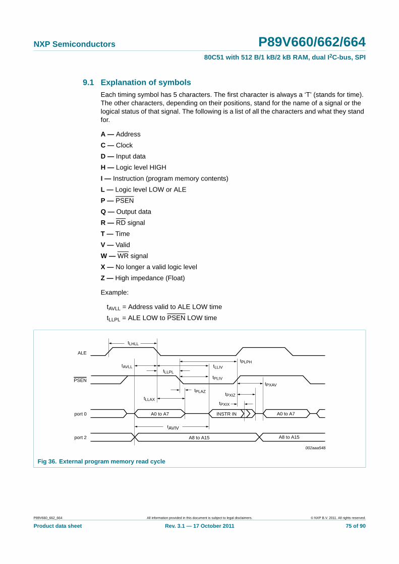
NXP Semiconductors P89V660/662/66480C51 with 512 B/1 kB/2 kB RAM, dual I2C-bus, SPI
9.1 Explanation of symbols
Each timing symbol has 5 characters. The first character is always a ‘T’ (stands for time). The other characters, depending on their positions, stand for the name of a signal or the logical status of that signal. The following is a list of all the characters and what they stand for.
A — Address
C — Clock
D — Input data
H — Logic level HIGH
I — Instruction (program memory contents)
L — Logic level LOW or ALE
P — PSEN
Q — Output data
R — RD signal
T — Time
V — Valid
W — WR signal
X — No longer a valid logic level
Z — High impedance (Float)
Example:
tAVLL = Address valid to ALE LOW time
tLLPL = ALE LOW to PSEN LOW time
Fig 36. External program memory read cycle
002aaa548
port 2
PSEN
ALE
A0 to A7
tLLAX
tPLAZtPXIZ
tLLPL
tAVIV
tAVLL tLLIV
tPLIV
tPLPH
INSTR IN
A8 to A15 A8 to A15
A0 to A7port 0
tPXIX
tPXAV
tLHLL
P89V660_662_664 All information provided in this document is subject to legal disclaimers. © NXP B.V. 2011. All rights reserved.
Product data sheet Rev. 3.1 — 17 October 2011 75 of 90

NXP Semiconductors P89V660/662/66480C51 with 512 B/1 kB/2 kB RAM, dual I2C-bus, SPI
Fig 37. External data memory read cycle
ALE
PSEN
port 0
port 2
RD
A0 to A7from RI to DPL DATA IN A0 to A7 from PCL INSTR IN
P2.0 to P2.7 or A8 to A15 from DPH A0 to A15 from PCH
tLLDV
002aaa549
tWHLH
tAVDV
tLLWL
tAVLL
tAVWL
tRLRH
tRLDV
tLLAX tRHDZ
tRHDXtRLAZ
Fig 38. External data memory write cycle
002aaa550
port 2
port 0
WR
PSEN
ALE
tLHLL
P2[7:0] or A8 to A15 from DPH
A0 to A7 from RI or DPL DATA OUT INSTR IN
tAVLL
tAVWL
tLLWL
tLLAX
tWLWH
tQVWH
tWHQX
tWHLH
A8 to A15 from PCH
A0 to A7 from PCL
P89V660_662_664 All information provided in this document is subject to legal disclaimers. © NXP B.V. 2011. All rights reserved.
Product data sheet Rev. 3.1 — 17 October 2011 76 of 90

NXP Semiconductors P89V660/662/66480C51 with 512 B/1 kB/2 kB RAM, dual I2C-bus, SPI
Table 72. External clock drive
Symbol Parameter Oscillator Unit
40 MHz Variable
Min Max Min Max
fosc oscillator frequency - - 0 40 MHz
Tcy(clk) clock cycle time 25 - - - ns
tCHCX clock HIGH time 8.75 - 0.35Tcy(clk) 0.65Tcy(clk) ns
tCLCX clock LOW time 8.75 - 0.35Tcy(clk) 0.65Tcy(clk) ns
tCLCH clock rise time - 10 - - ns
tCHCL clock fall time - 10 - - ns
Fig 39. External clock drive waveform
tCHCL tCLCX
tCHCX
Tcy(clk)
tCLCH
002aaa907
Table 73. Serial port timing
Symbol Parameter Oscillator Unit
40 MHz Variable
Min Max Min Max
TXLXL serial port clock cycle time 0.3 - 12Tcy(clk) - s
tQVXH output data set-up to clock rising edge time
117 - 10Tcy(clk) 133 - ns
tXHQX output data hold after clock rising edge time
0 - 2Tcy(clk) 50 - ns
tXHDX input data hold after clock rising edge time
0 - 0 - ns
tXHDV input data valid to clock rising edge time
- 117 - 10Tcy(clk) 133 ns
P89V660_662_664 All information provided in this document is subject to legal disclaimers. © NXP B.V. 2011. All rights reserved.
Product data sheet Rev. 3.1 — 17 October 2011 77 of 90
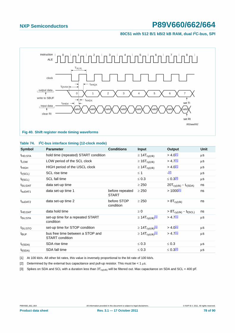
NXP Semiconductors P89V660/662/66480C51 with 512 B/1 kB/2 kB RAM, dual I2C-bus, SPI
[1] At 100 kb/s. All other bit rates, this value is inversely proportional to the bit rate of 100 kb/s.
[2] Determined by the external bus capacitance and pull-up resistor. This must be < 1 s.
[3] Spikes on SDA and SCL with a duration less than 3Tcy(clk) will be filtered out. Max capacitance on SDA and SCL = 400 pF.
Fig 40. Shift register mode timing waveforms
002aaa552
ALE
0instruction 1 2 3 4 5 6 7 8
0 1 2 3 4 5 6 7
valid valid valid valid valid valid valid valid
TXLXL
set TI
set RI
tXHQXtQVXH
tXHDV
tXHDX
clock
output data
write to SBUF
input data
clear RI
Table 74. I2C-bus interface timing (12-clock mode)
Symbol Parameter Conditions Input Output Unit
tHD;STA hold time (repeated) START condition 14Tcy(clk) > 4.0[1] s
tLOW LOW period of the SCL clock 16Tcy(clk) > 4.7[1] s
tHIGH HIGH period of the USCL clock 14Tcy(clk) > 4.0[1] s
tr(SCL) SCL rise time 1 -[2] s
tf(SCL) SCL fall time 0.3 0.3[3] s
tSU;DAT data set-up time 250 20Tcy(clk) tr(SDA) ns
tsuDAT1 data set-up time 1 before repeated START
250 > 1000[1] ns
tsuDAT2 data set-up time 2 before STOP condition
250 > 8Tcy(clk) ns
tHD;DAT data hold time 0 > 8Tcy(clk) tf(SCL) ns
tSU;STA set-up time for a repeated START condition
14Tcy(clk)[1] > 4.7[1] s
tSU;STO set-up time for STOP condition 14Tcy(clk)[1] > 4.0[1] s
tBUF bus free time between a STOP and START condition
14Tcy(clk)[1] > 4.7[1] s
tr(SDA) SDA rise time 0.3 0.3 s
tf(SDA) SDA fall time 0.3 0.3[3] s
P89V660_662_664 All information provided in this document is subject to legal disclaimers. © NXP B.V. 2011. All rights reserved.
Product data sheet Rev. 3.1 — 17 October 2011 78 of 90
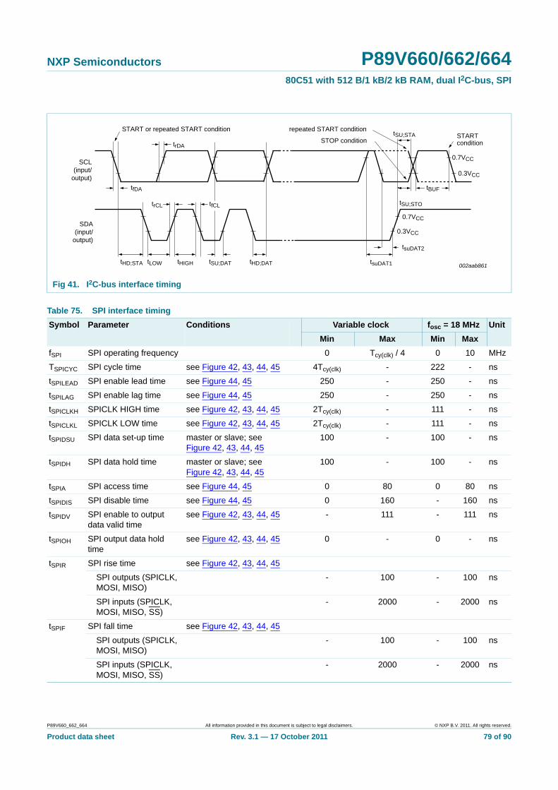
NXP Semiconductors P89V660/662/66480C51 with 512 B/1 kB/2 kB RAM, dual I2C-bus, SPI
Fig 41. I2C-bus interface timing
002aab861tHD;STA
trCL
trDA
tSU;STA
tLOW tHIGH tSU;DAT tHD;DAT tsuDAT1
SCL(input/
output)
SDA(input/
output)
START or repeated START condition
tfCL
0.7VCC
0.3VCC
tsuDAT2
tSU;STO
repeated START condition
STOP conditionSTART condition
0.7VCC
0.3VCC
tfDA tBUF
Table 75. SPI interface timing
Symbol Parameter Conditions Variable clock fosc = 18 MHz Unit
Min Max Min Max
fSPI SPI operating frequency 0 Tcy(clk) / 4 0 10 MHz
TSPICYC SPI cycle time see Figure 42, 43, 44, 45 4Tcy(clk) - 222 - ns
tSPILEAD SPI enable lead time see Figure 44, 45 250 - 250 - ns
tSPILAG SPI enable lag time see Figure 44, 45 250 - 250 - ns
tSPICLKH SPICLK HIGH time see Figure 42, 43, 44, 45 2Tcy(clk) - 111 - ns
tSPICLKL SPICLK LOW time see Figure 42, 43, 44, 45 2Tcy(clk) - 111 - ns
tSPIDSU SPI data set-up time master or slave; see Figure 42, 43, 44, 45
100 - 100 - ns
tSPIDH SPI data hold time master or slave; see Figure 42, 43, 44, 45
100 - 100 - ns
tSPIA SPI access time see Figure 44, 45 0 80 0 80 ns
tSPIDIS SPI disable time see Figure 44, 45 0 160 - 160 ns
tSPIDV SPI enable to output data valid time
see Figure 42, 43, 44, 45 - 111 - 111 ns
tSPIOH SPI output data hold time
see Figure 42, 43, 44, 45 0 - 0 - ns
tSPIR SPI rise time see Figure 42, 43, 44, 45
SPI outputs (SPICLK, MOSI, MISO)
- 100 - 100 ns
SPI inputs (SPICLK, MOSI, MISO, SS)
- 2000 - 2000 ns
tSPIF SPI fall time see Figure 42, 43, 44, 45
SPI outputs (SPICLK, MOSI, MISO)
- 100 - 100 ns
SPI inputs (SPICLK, MOSI, MISO, SS)
- 2000 - 2000 ns
P89V660_662_664 All information provided in this document is subject to legal disclaimers. © NXP B.V. 2011. All rights reserved.
Product data sheet Rev. 3.1 — 17 October 2011 79 of 90
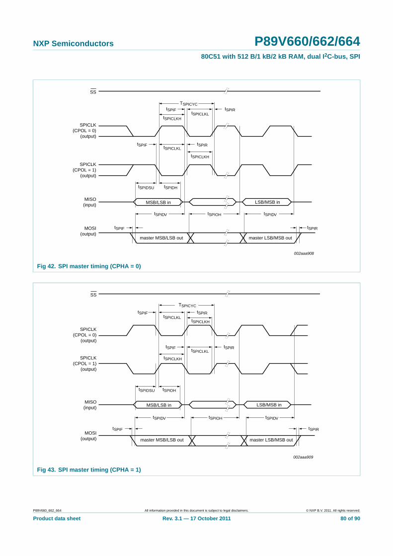
NXP Semiconductors P89V660/662/66480C51 with 512 B/1 kB/2 kB RAM, dual I2C-bus, SPI
Fig 42. SPI master timing (CPHA = 0)
TSPICYC
tSPICLKH
tSPICLKH
tSPICLKL
tSPICLKL
master LSB/MSB outmaster MSB/LSB out
tSPIDHtSPIDSU
tSPIF
tSPIOH tSPIDV
tSPIR
tSPIDV
tSPIF tSPIR
tSPIF tSPIR
SS
SPICLK(CPOL = 0)
(output)
002aaa908
SPICLK(CPOL = 1)
(output)
MISO(input)
MOSI(output)
LSB/MSB inMSB/LSB in
Fig 43. SPI master timing (CPHA = 1)
TSPICYC
tSPICLKL
tSPICLKL
tSPICLKH
tSPICLKH
master LSB/MSB outmaster MSB/LSB out
tSPIDHtSPIDSU
tSPIF
tSPIOH tSPIDV
tSPIR
tSPIDV
tSPIF
tSPIF
tSPIR
tSPIR
SS
SPICLK(CPOL = 0)
(output)
002aaa909
SPICLK(CPOL = 1)
(output)
MISO(input)
MOSI(output)
LSB/MSB inMSB/LSB in
P89V660_662_664 All information provided in this document is subject to legal disclaimers. © NXP B.V. 2011. All rights reserved.
Product data sheet Rev. 3.1 — 17 October 2011 80 of 90

NXP Semiconductors P89V660/662/66480C51 with 512 B/1 kB/2 kB RAM, dual I2C-bus, SPI
Fig 44. SPI slave timing (CPHA = 0)
TSPICYC
tSPICLKH
tSPICLKH
tSPICLKL
tSPICLKL
tSPILEAD tSPILAG
tSPIDSU tSPIDH tSPIDHtSPIDSU tSPIDSU
tSPIF
tSPIA tSPIOH tSPIDIS
tSPIR
slave MSB/LSB out
MSB/LSB in LSB/MSB in
slave LSB/MSB out
tSPIDV
tSPIOH tSPIOH
tSPIDV
tSPIR
tSPIR
tSPIF
tSPIF
SS
SPICLK(CPOL = 0)
(input)
002aaa910
SPICLK(CPOL = 1)
(input)
MISO(output)
MOSI(input)
not defined
Fig 45. SPI slave timing (CPHA = 1)
002aaa911
TSPICYC
tSPICLKH
tSPICLKH
tSPICLKLtSPILEAD
tSPICLKL
tSPILAG
tSPIDSU tSPIDSUtSPIDH tSPIDH
tSPIF tSPIR
tSPIR
tSPIA
tSPIOH tSPIOH tSPIOH
tSPIDIS
slave MSB/LSB outnot defined
MSB/LSB in LSB/MSB in
slave LSB/MSB out
tSPIDV tSPIDV tSPIDV
tSPIRtSPIF
tSPIF
SS
SPICLK(CPOL = 0)
(input)
SPICLK(CPOL = 1)
(input)
MISO(output)
MOSI(input)
P89V660_662_664 All information provided in this document is subject to legal disclaimers. © NXP B.V. 2011. All rights reserved.
Product data sheet Rev. 3.1 — 17 October 2011 81 of 90
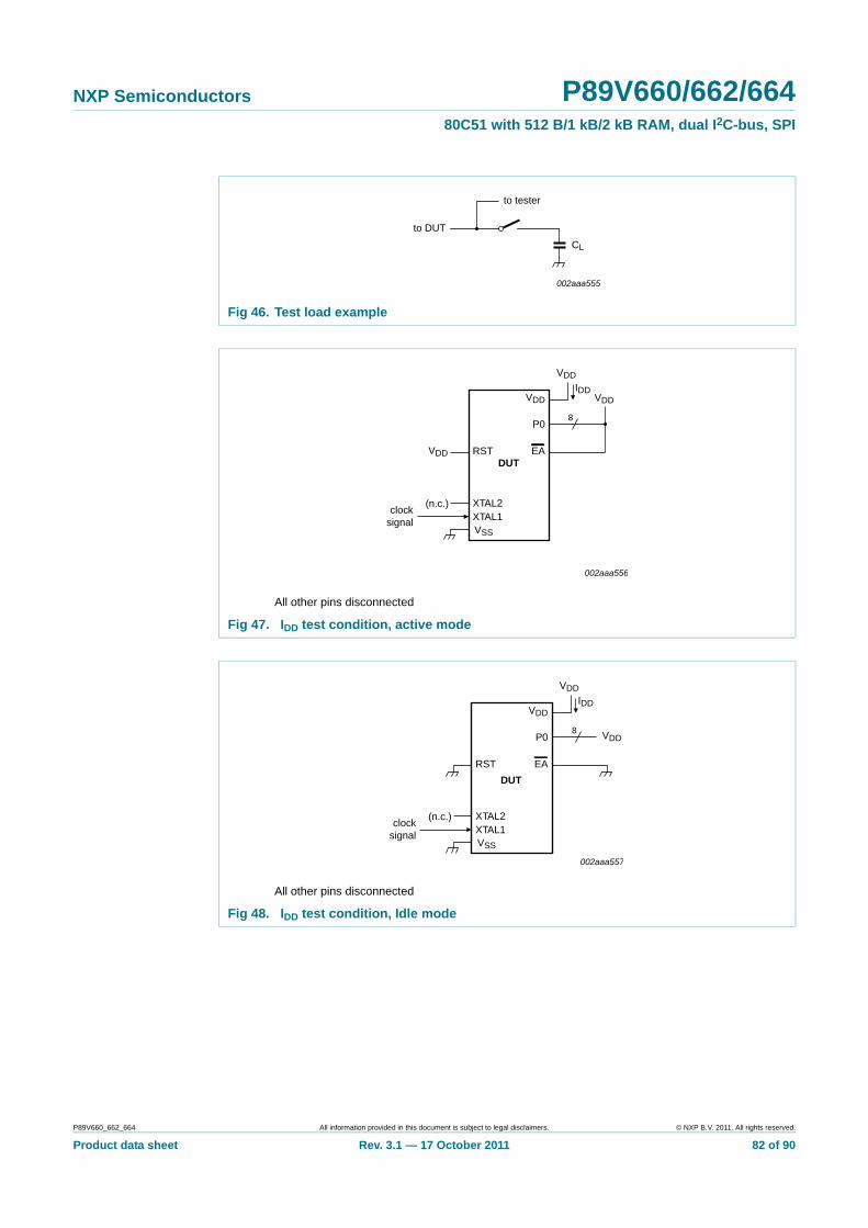
NXP Semiconductors P89V660/662/66480C51 with 512 B/1 kB/2 kB RAM, dual I2C-bus, SPI
Fig 46. Test load example
All other pins disconnected
Fig 47. IDD test condition, active mode
All other pins disconnected
Fig 48. IDD test condition, Idle mode
002aaa555
to DUT
to tester
CL
002aaa556
VDD
VDD
VDD
P0
EARST
XTAL2(n.c.)clock
signal XTAL1VSS
IDD
VDD
8
DUT
002aaa557
VDD
VDD
VDD
P0
EARST
XTAL2(n.c.)clock
signal XTAL1VSS
IDD
8
DUT
P89V660_662_664 All information provided in this document is subject to legal disclaimers. © NXP B.V. 2011. All rights reserved.
Product data sheet Rev. 3.1 — 17 October 2011 82 of 90
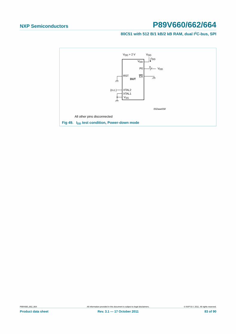
NXP Semiconductors P89V660/662/66480C51 with 512 B/1 kB/2 kB RAM, dual I2C-bus, SPI
All other pins disconnected
Fig 49. IDD test condition, Power-down mode
002aaa558
VDDVDD = 2 V
VDD
P0
EARST
XTAL2(n.c.)XTAL1VSS
IDD
VDD8
DUT
P89V660_662_664 All information provided in this document is subject to legal disclaimers. © NXP B.V. 2011. All rights reserved.
Product data sheet Rev. 3.1 — 17 October 2011 83 of 90
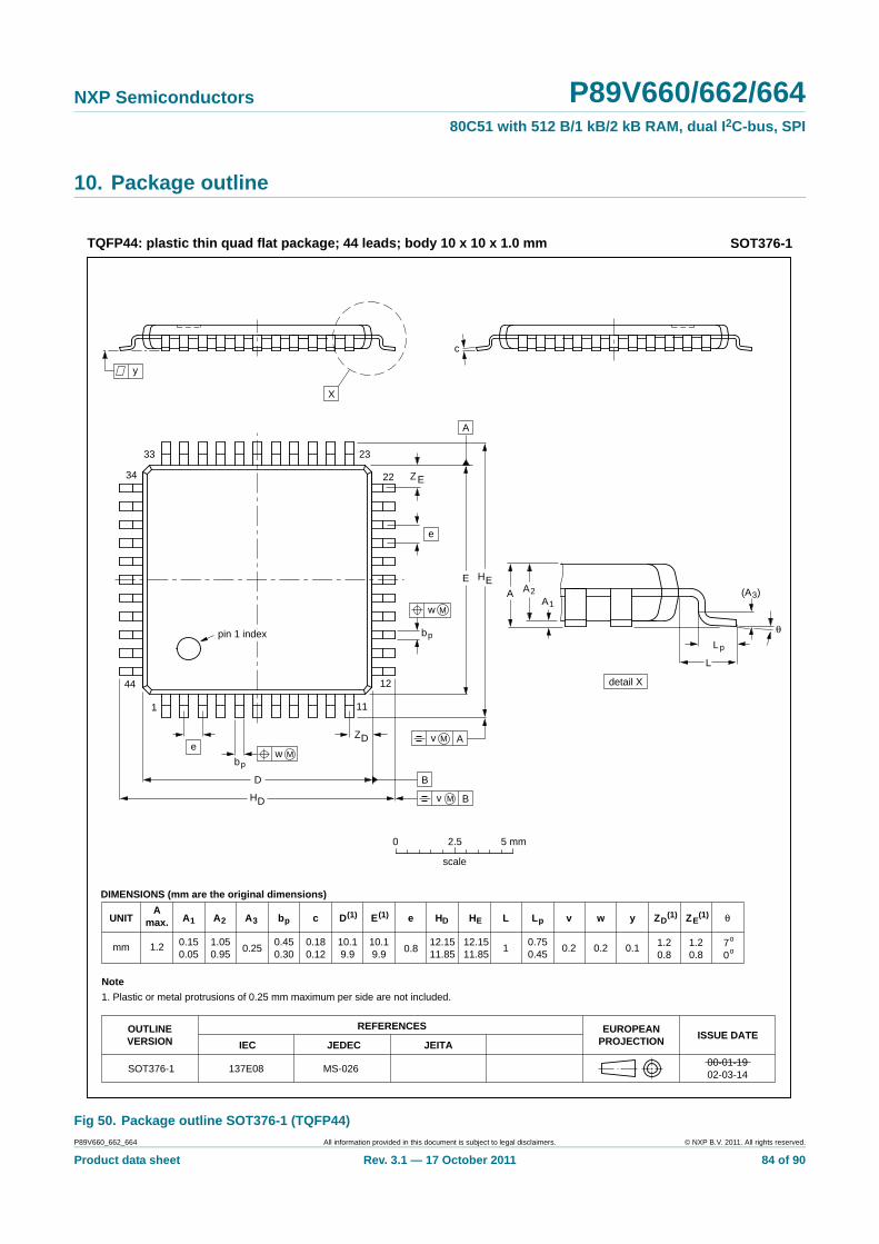
NXP Semiconductors P89V660/662/66480C51 with 512 B/1 kB/2 kB RAM, dual I2C-bus, SPI
10. Package outline
Fig 50. Package outline SOT376-1 (TQFP44)
UNITA
max. A1 A2 A3 bp c E(1) e HE L Lp Zywv θ
REFERENCESOUTLINEVERSION
EUROPEANPROJECTION ISSUE DATE
IEC JEDEC JEITA
mm 1.2 0.150.05
1.050.95
0.250.450.30
0.180.12
10.19.9 0.8
12.1511.85
1.20.8
70
o
o0.2 0.10.21
DIMENSIONS (mm are the original dimensions)
Note
1. Plastic or metal protrusions of 0.25 mm maximum per side are not included.
0.750.45
SOT376-1 137E08 MS-02600-01-1902-03-14
D(1) (1)(1)
10.19.9
HD
12.1511.85
EZ
1.20.8
D
bp
e
E
B
11
DH
bp
EH
v M B
D
ZD
A
ZE
e
v M A
1
44
34
33 23
22
12
θ
A1A
Lp
detail X
L
(A )3A2
X
y
c
w M
w M
0 2.5 5 mm
scale
TQFP44: plastic thin quad flat package; 44 leads; body 10 x 10 x 1.0 mm SOT376-1
pin 1 index
P89V660_662_664 All information provided in this document is subject to legal disclaimers. © NXP B.V. 2011. All rights reserved.
Product data sheet Rev. 3.1 — 17 October 2011 84 of 90
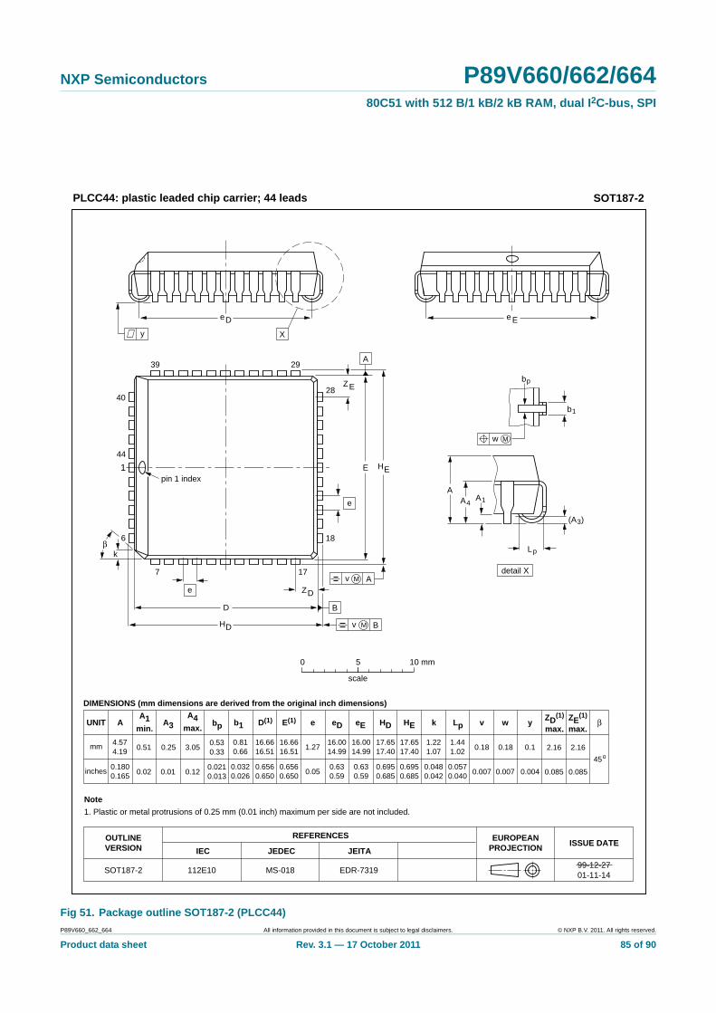
NXP Semiconductors P89V660/662/66480C51 with 512 B/1 kB/2 kB RAM, dual I2C-bus, SPI
Fig 51. Package outline SOT187-2 (PLCC44)
UNIT AA1
min.
A4max.
bp e ywv β
REFERENCESOUTLINEVERSION
EUROPEANPROJECTION ISSUE DATE
IEC JEDEC JEITA
mm 4.574.19 0.51 3.05
0.530.33
0.0210.013
16.6616.51
1.2717.6517.40 2.16
45o0.18 0.10.18
DIMENSIONS (mm dimensions are derived from the original inch dimensions)
Note
1. Plastic or metal protrusions of 0.25 mm (0.01 inch) maximum per side are not included.
SOT187-2
D(1) E(1)
16.6616.51
HD HE
17.6517.40
ZD(1)
max.ZE
(1)
max.
2.16
b1
0.810.66
k
1.221.07
0.1800.165 0.02 0.12
A3
0.25
0.010.6560.650
0.050.6950.685 0.0850.007 0.0040.007
Lp
1.441.02
0.0570.040
0.6560.650
0.6950.685
eD eE
16.0014.99
0.630.59
16.0014.99
0.630.59 0.085
0.0320.026
0.0480.042
2939
44
1
6
7 17
28
18
40
detail X
(A )3
bp
w M
A1A
A4
Lp
b1
βk
Xy
e
E
B
DH
Ee
EH
v M B
D
ZD
A
ZE
e
v M A
pin 1 index
112E10 MS-018 EDR-7319
0 5 10 mm
scale
99-12-2701-11-14
inches
PLCC44: plastic leaded chip carrier; 44 leads SOT187-2
De
P89V660_662_664 All information provided in this document is subject to legal disclaimers. © NXP B.V. 2011. All rights reserved.
Product data sheet Rev. 3.1 — 17 October 2011 85 of 90
NXP Semiconductors P89V660/662/66480C51 with 512 B/1 kB/2 kB RAM, dual I2C-bus, SPI
11. Abbreviations
Table 76. Acronym list
Acronym Description
ALE Address Latch Enabled
CPU Central Processing Unit
DUT Device Under Test
EPROM Erasable Programmable Read-Only Memory
EMI Electro-Magnetic Interference
MCU Microcontroller Unit
PWM Pulse Width Modulator
RAM Random Access Memory
RC Resistance-Capacitance
SFR Special Function Register
SPI Serial Peripheral Interface
UART Universal Asynchronous Receiver/Transmitter
P89V660_662_664 All information provided in this document is subject to legal disclaimers. © NXP B.V. 2011. All rights reserved.
Product data sheet Rev. 3.1 — 17 October 2011 86 of 90
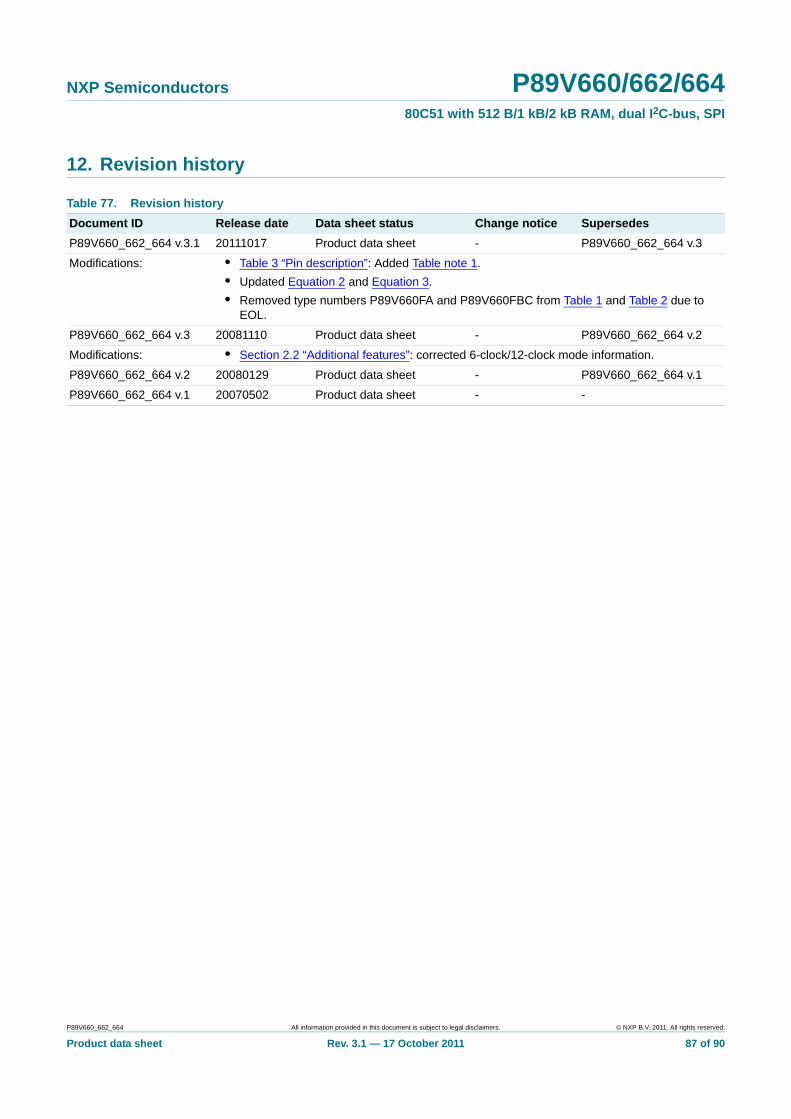
NXP Semiconductors P89V660/662/66480C51 with 512 B/1 kB/2 kB RAM, dual I2C-bus, SPI
12. Revision history
Table 77. Revision history
Document ID Release date Data sheet status Change notice Supersedes
P89V660_662_664 v.3.1 20111017 Product data sheet - P89V660_662_664 v.3
Modifications: • Table 3 “Pin description”: Added Table note 1.
• Updated Equation 2 and Equation 3.
• Removed type numbers P89V660FA and P89V660FBC from Table 1 and Table 2 due to EOL.
P89V660_662_664 v.3 20081110 Product data sheet - P89V660_662_664 v.2
Modifications: • Section 2.2 “Additional features”: corrected 6-clock/12-clock mode information.
P89V660_662_664 v.2 20080129 Product data sheet - P89V660_662_664 v.1
P89V660_662_664 v.1 20070502 Product data sheet - -
P89V660_662_664 All information provided in this document is subject to legal disclaimers. © NXP B.V. 2011. All rights reserved.
Product data sheet Rev. 3.1 — 17 October 2011 87 of 90

NXP Semiconductors P89V660/662/66480C51 with 512 B/1 kB/2 kB RAM, dual I2C-bus, SPI
13. Legal information
13.1 Data sheet status
[1] Please consult the most recently issued document before initiating or completing a design.
[2] The term ‘short data sheet’ is explained in section “Definitions”.
[3] The product status of device(s) described in this document may have changed since this document was published and may differ in case of multiple devices. The latest product status information is available on the Internet at URL http://www.nxp.com.
13.2 Definitions
Draft — The document is a draft version only. The content is still under internal review and subject to formal approval, which may result in modifications or additions. NXP Semiconductors does not give any representations or warranties as to the accuracy or completeness of information included herein and shall have no liability for the consequences of use of such information.
Short data sheet — A short data sheet is an extract from a full data sheet with the same product type number(s) and title. A short data sheet is intended for quick reference only and should not be relied upon to contain detailed and full information. For detailed and full information see the relevant full data sheet, which is available on request via the local NXP Semiconductors sales office. In case of any inconsistency or conflict with the short data sheet, the full data sheet shall prevail.
Product specification — The information and data provided in a Product data sheet shall define the specification of the product as agreed between NXP Semiconductors and its customer, unless NXP Semiconductors and customer have explicitly agreed otherwise in writing. In no event however, shall an agreement be valid in which the NXP Semiconductors product is deemed to offer functions and qualities beyond those described in the Product data sheet.
13.3 Disclaimers
Limited warranty and liability — Information in this document is believed to be accurate and reliable. However, NXP Semiconductors does not give any representations or warranties, expressed or implied, as to the accuracy or completeness of such information and shall have no liability for the consequences of use of such information.
In no event shall NXP Semiconductors be liable for any indirect, incidental, punitive, special or consequential damages (including - without limitation - lost profits, lost savings, business interruption, costs related to the removal or replacement of any products or rework charges) whether or not such damages are based on tort (including negligence), warranty, breach of contract or any other legal theory.
Notwithstanding any damages that customer might incur for any reason whatsoever, NXP Semiconductors’ aggregate and cumulative liability towards customer for the products described herein shall be limited in accordance with the Terms and conditions of commercial sale of NXP Semiconductors.
Right to make changes — NXP Semiconductors reserves the right to make changes to information published in this document, including without limitation specifications and product descriptions, at any time and without notice. This document supersedes and replaces all information supplied prior to the publication hereof.
Suitability for use — NXP Semiconductors products are not designed, authorized or warranted to be suitable for use in life support, life-critical or safety-critical systems or equipment, nor in applications where failure or
malfunction of an NXP Semiconductors product can reasonably be expected to result in personal injury, death or severe property or environmental damage. NXP Semiconductors accepts no liability for inclusion and/or use of NXP Semiconductors products in such equipment or applications and therefore such inclusion and/or use is at the customer’s own risk.
Applications — Applications that are described herein for any of these products are for illustrative purposes only. NXP Semiconductors makes no representation or warranty that such applications will be suitable for the specified use without further testing or modification.
Customers are responsible for the design and operation of their applications and products using NXP Semiconductors products, and NXP Semiconductors accepts no liability for any assistance with applications or customer product design. It is customer’s sole responsibility to determine whether the NXP Semiconductors product is suitable and fit for the customer’s applications and products planned, as well as for the planned application and use of customer’s third party customer(s). Customers should provide appropriate design and operating safeguards to minimize the risks associated with their applications and products.
NXP Semiconductors does not accept any liability related to any default, damage, costs or problem which is based on any weakness or default in the customer’s applications or products, or the application or use by customer’s third party customer(s). Customer is responsible for doing all necessary testing for the customer’s applications and products using NXP Semiconductors products in order to avoid a default of the applications and the products or of the application or use by customer’s third party customer(s). NXP does not accept any liability in this respect.
Limiting values — Stress above one or more limiting values (as defined in the Absolute Maximum Ratings System of IEC 60134) will cause permanent damage to the device. Limiting values are stress ratings only and (proper) operation of the device at these or any other conditions above those given in the Recommended operating conditions section (if present) or the Characteristics sections of this document is not warranted. Constant or repeated exposure to limiting values will permanently and irreversibly affect the quality and reliability of the device.
Terms and conditions of commercial sale — NXP Semiconductors products are sold subject to the general terms and conditions of commercial sale, as published at http://www.nxp.com/profile/terms, unless otherwise agreed in a valid written individual agreement. In case an individual agreement is concluded only the terms and conditions of the respective agreement shall apply. NXP Semiconductors hereby expressly objects to applying the customer’s general terms and conditions with regard to the purchase of NXP Semiconductors products by customer.
No offer to sell or license — Nothing in this document may be interpreted or construed as an offer to sell products that is open for acceptance or the grant, conveyance or implication of any license under any copyrights, patents or other industrial or intellectual property rights.
Export control — This document as well as the item(s) described herein may be subject to export control regulations. Export might require a prior authorization from competent authorities.
Document status[1][2] Product status[3] Definition
Objective [short] data sheet Development This document contains data from the objective specification for product development.
Preliminary [short] data sheet Qualification This document contains data from the preliminary specification.
Product [short] data sheet Production This document contains the product specification.
P89V660_662_664 All information provided in this document is subject to legal disclaimers. © NXP B.V. 2011. All rights reserved.
Product data sheet Rev. 3.1 — 17 October 2011 88 of 90

NXP Semiconductors P89V660/662/66480C51 with 512 B/1 kB/2 kB RAM, dual I2C-bus, SPI
Non-automotive qualified products — Unless this data sheet expressly states that this specific NXP Semiconductors product is automotive qualified, the product is not suitable for automotive use. It is neither qualified nor tested in accordance with automotive testing or application requirements. NXP Semiconductors accepts no liability for inclusion and/or use of non-automotive qualified products in automotive equipment or applications.
In the event that customer uses the product for design-in and use in automotive applications to automotive specifications and standards, customer (a) shall use the product without NXP Semiconductors’ warranty of the product for such automotive applications, use and specifications, and (b) whenever customer uses the product for automotive applications beyond NXP Semiconductors’ specifications such use shall be solely at customer’s
own risk, and (c) customer fully indemnifies NXP Semiconductors for any liability, damages or failed product claims resulting from customer design and use of the product for automotive applications beyond NXP Semiconductors’ standard warranty and NXP Semiconductors’ product specifications.
13.4 TrademarksNotice: All referenced brands, product names, service names and trademarks are the property of their respective owners.
I2C-bus — logo is a trademark of NXP B.V.
14. Contact information
For more information, please visit: http://www.nxp.com
For sales office addresses, please send an email to: [email protected]
P89V660_662_664 All information provided in this document is subject to legal disclaimers. © NXP B.V. 2011. All rights reserved.
Product data sheet Rev. 3.1 — 17 October 2011 89 of 90
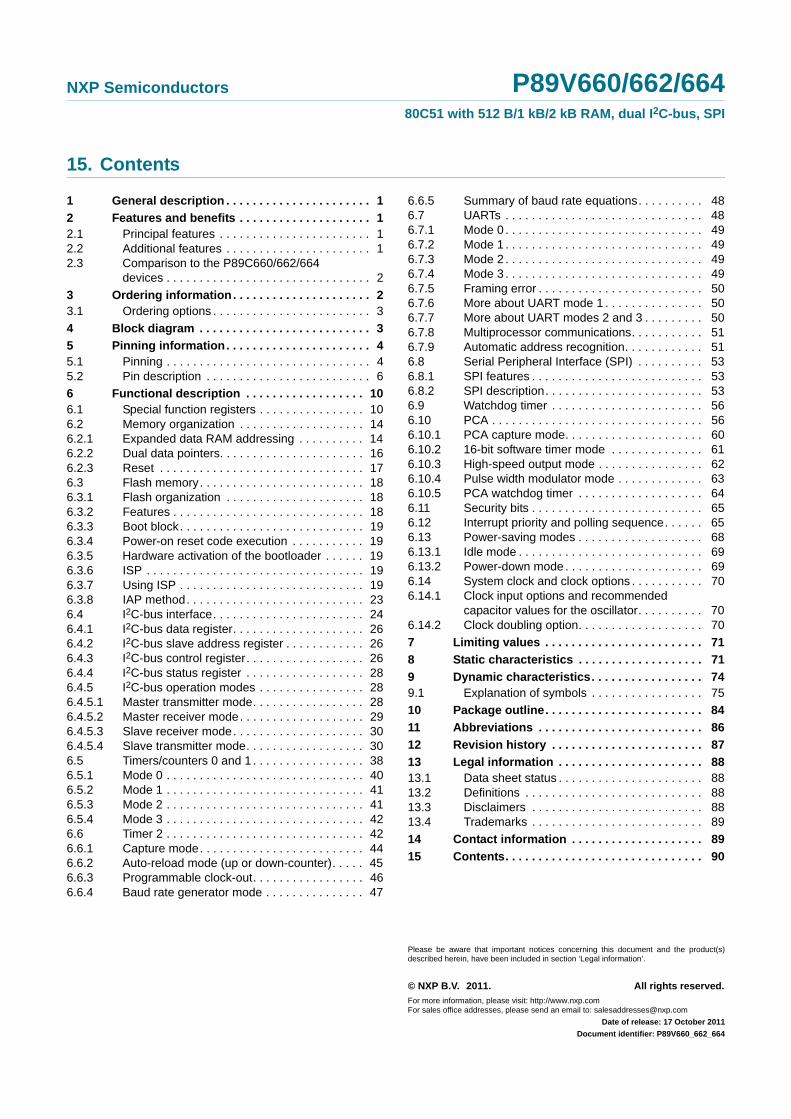
NXP Semiconductors P89V660/662/66480C51 with 512 B/1 kB/2 kB RAM, dual I2C-bus, SPI
15. Contents
1 General description . . . . . . . . . . . . . . . . . . . . . . 1
2 Features and benefits . . . . . . . . . . . . . . . . . . . . 12.1 Principal features . . . . . . . . . . . . . . . . . . . . . . . 12.2 Additional features . . . . . . . . . . . . . . . . . . . . . . 12.3 Comparison to the P89C660/662/664
devices . . . . . . . . . . . . . . . . . . . . . . . . . . . . . . . 2
3 Ordering information. . . . . . . . . . . . . . . . . . . . . 23.1 Ordering options . . . . . . . . . . . . . . . . . . . . . . . . 3
4 Block diagram . . . . . . . . . . . . . . . . . . . . . . . . . . 3
5 Pinning information. . . . . . . . . . . . . . . . . . . . . . 45.1 Pinning . . . . . . . . . . . . . . . . . . . . . . . . . . . . . . . 45.2 Pin description . . . . . . . . . . . . . . . . . . . . . . . . . 6
6 Functional description . . . . . . . . . . . . . . . . . . 106.1 Special function registers . . . . . . . . . . . . . . . . 106.2 Memory organization . . . . . . . . . . . . . . . . . . . 146.2.1 Expanded data RAM addressing . . . . . . . . . . 146.2.2 Dual data pointers. . . . . . . . . . . . . . . . . . . . . . 166.2.3 Reset . . . . . . . . . . . . . . . . . . . . . . . . . . . . . . . 176.3 Flash memory. . . . . . . . . . . . . . . . . . . . . . . . . 186.3.1 Flash organization . . . . . . . . . . . . . . . . . . . . . 186.3.2 Features . . . . . . . . . . . . . . . . . . . . . . . . . . . . . 186.3.3 Boot block. . . . . . . . . . . . . . . . . . . . . . . . . . . . 196.3.4 Power-on reset code execution . . . . . . . . . . . 196.3.5 Hardware activation of the bootloader . . . . . . 196.3.6 ISP . . . . . . . . . . . . . . . . . . . . . . . . . . . . . . . . . 196.3.7 Using ISP . . . . . . . . . . . . . . . . . . . . . . . . . . . . 196.3.8 IAP method. . . . . . . . . . . . . . . . . . . . . . . . . . . 236.4 I2C-bus interface. . . . . . . . . . . . . . . . . . . . . . . 246.4.1 I2C-bus data register. . . . . . . . . . . . . . . . . . . . 266.4.2 I2C-bus slave address register . . . . . . . . . . . . 266.4.3 I2C-bus control register. . . . . . . . . . . . . . . . . . 266.4.4 I2C-bus status register . . . . . . . . . . . . . . . . . . 286.4.5 I2C-bus operation modes . . . . . . . . . . . . . . . . 286.4.5.1 Master transmitter mode. . . . . . . . . . . . . . . . . 286.4.5.2 Master receiver mode. . . . . . . . . . . . . . . . . . . 296.4.5.3 Slave receiver mode. . . . . . . . . . . . . . . . . . . . 306.4.5.4 Slave transmitter mode. . . . . . . . . . . . . . . . . . 306.5 Timers/counters 0 and 1 . . . . . . . . . . . . . . . . . 386.5.1 Mode 0 . . . . . . . . . . . . . . . . . . . . . . . . . . . . . . 406.5.2 Mode 1 . . . . . . . . . . . . . . . . . . . . . . . . . . . . . . 416.5.3 Mode 2 . . . . . . . . . . . . . . . . . . . . . . . . . . . . . . 416.5.4 Mode 3 . . . . . . . . . . . . . . . . . . . . . . . . . . . . . . 426.6 Timer 2 . . . . . . . . . . . . . . . . . . . . . . . . . . . . . . 426.6.1 Capture mode. . . . . . . . . . . . . . . . . . . . . . . . . 446.6.2 Auto-reload mode (up or down-counter). . . . . 456.6.3 Programmable clock-out. . . . . . . . . . . . . . . . . 466.6.4 Baud rate generator mode . . . . . . . . . . . . . . . 47
6.6.5 Summary of baud rate equations. . . . . . . . . . 486.7 UARTs . . . . . . . . . . . . . . . . . . . . . . . . . . . . . . 486.7.1 Mode 0 . . . . . . . . . . . . . . . . . . . . . . . . . . . . . . 496.7.2 Mode 1 . . . . . . . . . . . . . . . . . . . . . . . . . . . . . . 496.7.3 Mode 2 . . . . . . . . . . . . . . . . . . . . . . . . . . . . . . 496.7.4 Mode 3 . . . . . . . . . . . . . . . . . . . . . . . . . . . . . . 496.7.5 Framing error . . . . . . . . . . . . . . . . . . . . . . . . . 506.7.6 More about UART mode 1 . . . . . . . . . . . . . . . 506.7.7 More about UART modes 2 and 3 . . . . . . . . . 506.7.8 Multiprocessor communications. . . . . . . . . . . 516.7.9 Automatic address recognition. . . . . . . . . . . . 516.8 Serial Peripheral Interface (SPI) . . . . . . . . . . 536.8.1 SPI features . . . . . . . . . . . . . . . . . . . . . . . . . . 536.8.2 SPI description. . . . . . . . . . . . . . . . . . . . . . . . 536.9 Watchdog timer . . . . . . . . . . . . . . . . . . . . . . . 566.10 PCA . . . . . . . . . . . . . . . . . . . . . . . . . . . . . . . . 566.10.1 PCA capture mode. . . . . . . . . . . . . . . . . . . . . 606.10.2 16-bit software timer mode . . . . . . . . . . . . . . 616.10.3 High-speed output mode . . . . . . . . . . . . . . . . 626.10.4 Pulse width modulator mode . . . . . . . . . . . . . 636.10.5 PCA watchdog timer . . . . . . . . . . . . . . . . . . . 646.11 Security bits . . . . . . . . . . . . . . . . . . . . . . . . . . 656.12 Interrupt priority and polling sequence. . . . . . 656.13 Power-saving modes . . . . . . . . . . . . . . . . . . . 686.13.1 Idle mode . . . . . . . . . . . . . . . . . . . . . . . . . . . . 696.13.2 Power-down mode . . . . . . . . . . . . . . . . . . . . . 696.14 System clock and clock options . . . . . . . . . . . 706.14.1 Clock input options and recommended
capacitor values for the oscillator. . . . . . . . . . 706.14.2 Clock doubling option. . . . . . . . . . . . . . . . . . . 70
7 Limiting values . . . . . . . . . . . . . . . . . . . . . . . . 71
8 Static characteristics . . . . . . . . . . . . . . . . . . . 71
9 Dynamic characteristics. . . . . . . . . . . . . . . . . 749.1 Explanation of symbols . . . . . . . . . . . . . . . . . 75
10 Package outline. . . . . . . . . . . . . . . . . . . . . . . . 84
11 Abbreviations . . . . . . . . . . . . . . . . . . . . . . . . . 86
12 Revision history . . . . . . . . . . . . . . . . . . . . . . . 87
13 Legal information . . . . . . . . . . . . . . . . . . . . . . 8813.1 Data sheet status . . . . . . . . . . . . . . . . . . . . . . 8813.2 Definitions . . . . . . . . . . . . . . . . . . . . . . . . . . . 8813.3 Disclaimers . . . . . . . . . . . . . . . . . . . . . . . . . . 8813.4 Trademarks . . . . . . . . . . . . . . . . . . . . . . . . . . 89
14 Contact information . . . . . . . . . . . . . . . . . . . . 89
15 Contents. . . . . . . . . . . . . . . . . . . . . . . . . . . . . . 90
© NXP B.V. 2011. All rights reserved.
For more information, please visit: http://www.nxp.comFor sales office addresses, please send an email to: [email protected]
Date of release: 17 October 2011
Document identifier: P89V660_662_664
Please be aware that important notices concerning this document and the product(s)described herein, have been included in section ‘Legal information’.