package guide v5.0.prn - d3uzseaevmutz1.cloudfront.net · 3.17 8-pin ssop ... vide the ramp-up,...
TRANSCRIPT

JUN ‘01
High-Performance Packaging
Copyright 2001 — Cirrus Logic Inc. All rights reserved.This document describes a potential application of Cirrus Logic Inc. integrated circuits. No warranty is given for the suitability of the circuitry or program code described herein for any purpose other than demonstrating functional
operation. The information contained in this document is subject to change without notice.
Package Information Guide
Version 5.0
Scope and Applicability
This Package Information Guide presents informationabout Cirrus Logic product package selection andavailability.
Related Documents
Data books for specific products Quality and Reliability Quarterly Reports
JUN ‘01 2
High-Performance Packaging
Notice
The information in this Package Information Guide has beencarefully checked and is believed to be accurate. However, CirrusLogic Inc. reserves the right to make changes without further noticeto any products herein to improve reliability, function, or design, andmakes no guarantee or warranty concerning the accuracy of saidinformation, and shall not be responsible for any loss or damage ofwhatever nature resulting from the use of, or reliance upon, thisdocument.
Cirrus Logic Inc. also does not guarantee that the use of any infor-mation contained herein will not infringe upon the patent or otherrights of third parties, and no patent or other license is impliedhereby. This document does not, in any way, extend our warrantyon any products or specification beyond that set forth in its standardterms and conditions of sale.

JUN ‘01
High-Performance Packaging
Copyright 2001 — Cirrus Logic Inc. All rights reserved.This document describes a potential application of Cirrus Logic Inc. integrated circuits. No warranty is given for the suitability of the circuitry or program code described herein for any purpose other than demonstrating functional
operation. The information contained in this document is subject to change without notice.
1. INTRODUCTION......................................................................................................................41.1 Cirrus Logic Packages ...........................................................................................................................41.2 Plastic Package Materials ......................................................................................................................51.3 Assembly Die Pad Design Rules .........................................................................................................111.4 Package Thermal Resistance ..............................................................................................................131.5 Package Electrical Characteristics.......................................................................................................14
2. PACKAGE OUTLINE DRAWINGS.......................................................................................152.1 20-, 28-, 44-, 68-, and 84-Pin PLCC ....................................................................................................152.2 32-Pin LQFP .......................................................................................................................................172.3 44-Pin LQFP ........................................................................................................................................182.4 48-Pin LQFP ........................................................................................................................................192.5 64-Pin LQFP ........................................................................................................................................202.6 80-Pin TQFP (12 × 12 × 1.00-mm Body) .............................................................................................212.7 100-Pin MQFP (14 × 20 × 2.70-mm Body) ..........................................................................................222.8 100-Pin LQFP (14 × 14 × 1.40-mm Body)............................................................................................232.9 120-Pin LQFP (14 × 14 × 1.40-mm Body) ................................................................................................................... 24
2.10 128-Pin MQFP (28 × 28 × 3.50-mm Body)...........................................................................................252.11 128-Pin MQFP (14 × 20 × 2.70-mm Body)...........................................................................................262.12 128-Pin LQFP (14 × 14 × 1.40-mm Body)............................................................................................272.13 128-Pin LQFP (14 × 20 × 1.40-mm Body)............................................................................................282.14 144-Pin MQFP (28 × 28 × 3.50-mm Body)...........................................................................................292.15 144-Pin LQFP (20 × 20 × 1.40-mm Body)............................................................................................302.16 160-Pin MQFP (28 × 28 × 3.50-mm Body)...........................................................................................312.17 176-Pin LQFP (20 × 20 × 1.40-mm Body) ................................................................................................................... 32
2.18 176-Pin LQFP (24 × 24 × 1.40-mm Body)............................................................................................332.19 184-Pin LQFP (20 × 20 × 1.40-mm Body)............................................................................................342.20 208-Pin MQFP (28 × 28 × 3.50-mm Body)...........................................................................................352.21 208-Pin LQFP (28 × 28 × 1.40-mm Body)............................................................................................362.22 240-Pin MQFP 32 × 32 × 3.50-mm Body)............................................................................................372.23 256-Pin MQFP (28 × 28 × 3.50-mm Body) .................................................................................................................. 38
2.24 256-Pin LQFP (28 × 28 × 2.00-mm Body) ................................................................................................................... 39
2.25 256-Pin PBGA (27 × 27 × 1.60-mm Body) ...........................................................................................402.26 256-Pin PBGA (17 × 17 × 1.53-mm Body) ...........................................................................................412.27 144-Pin FBGA (12 × 12 × 1.20-mm Body) ...........................................................................................42
3. PACKAGE DRAWINGS – CRYSTAL SEMICONDUCTOR PRODUCTS DIVISION ..........433.1 8-Pin PDIP (300 -mm Body) ................................................................................................................433.2 14-Pin PDIP .........................................................................................................................................443.3 16-Pin PDIP .........................................................................................................................................453.4 18-Pin PDIP .........................................................................................................................................463.5 20-Pin PDIP .........................................................................................................................................473.6 24-Pin Skinny PDIP..............................................................................................................................483.7 24-Pin PDIP (600-mm Body)................................................................................................................493.8 28-Pin PDIP (600-mm Body)................................................................................................................50

JUN ‘01 2PACKAGE INFORMATION GUIDE v5.0
High-Performance Packaging
3.9 40-Pin PDIP (600-mm Body)................................................................................................................513.10 8-Pin SOIC (150-mm Body) .................................................................................................................523.11 8-Pin SOIC (209-mm Body) .................................................................................................................533.12 16-Pin SOIC (150-mm Body) ...............................................................................................................543.13 16-Pin SOIC (300-mm Body) ...............................................................................................................553.14 20-Pin SOIC (300-mm Body) ...............................................................................................................563.15 24-Pin SOIC (300-mm Body) ...............................................................................................................573.16 28-Pin SOIC (300-mm Body) ...............................................................................................................583.17 8-Pin SSOP..........................................................................................................................................593.18 16-Pin SSOP........................................................................................................................................603.19 20-Pin SSOP........................................................................................................................................613.20 24-Pin SSOP........................................................................................................................................623.21 28-Pin SSOP........................................................................................................................................633.22 16L TSSOP (4.4-mm Body) .................................................................................................................643.23 20L TSSOP (4.4-mm Body) ................................................................................................................653.24 24L TSSOP (4.4-mm Body) ................................................................................................................663.25 48-Pin TSSOP (6.1-mm Body).............................................................................................................673.26 44-Pin TQFP ........................................................................................................................................683.27 48-Pin TQFP ........................................................................................................................................693.28 64-Pin TQFP ........................................................................................................................................703.29 100-Pin TQFP ......................................................................................................................................713.30 100-Pin MQFP .....................................................................................................................................723.31 128-Pin TQFP ......................................................................................................................................733.32 144-Pin TQFP .....................................................................................................................................743.33 28-Pin PLCC ........................................................................................................................................753.34 44-Pin PLCC ........................................................................................................................................763.35 68-Pin PLCC ........................................................................................................................................77
4. TRAY DRAWINGS.................................................................................................................784.1 10 × 10 × 1.4-mm Body LQFP Tray .....................................................................................................784.2 10 × 10 × 1.0-mm Body TQFP Tray .....................................................................................................794.3 12 × 12 × 1.0-mm Body TQFP Tray .....................................................................................................804.4 14 × 20 × 2.7-mm Body MQFP Tray ....................................................................................................814.5 28 × 28 × 3.5-mm Body MQFP Tray ....................................................................................................824.6 32 × 32 × 3.5-mm Body MQFP Tray ....................................................................................................834.7 14 × 14 × 1.4-mm Body LQFP Tray .....................................................................................................844.8 14 × 20 × 1.4-mm Body LQFP Tray .....................................................................................................854.9 24 × 24 × 1.40-mm Body LQFP Tray ...................................................................................................864.10 28 × 28 × 1.40-mm Body LQFP Tray ...................................................................................................874.11 28 × 28 × 2.00-mm Body LQFP Tray ...................................................................................................884.12 27 × 27 × 1.60-mm Body BGA Tray .....................................................................................................894.13 17 × 17 × 1.53-mm Body BGA Tray .....................................................................................................904.14 12 × 12 × 1.20-mm Body BGA Tray .....................................................................................................91
5. TECHNOLOGY ROADMAP..................................................................................................92
6. QFP HANDLING/DRY PACK INFORMATION.....................................................................926.1 QFP Dry Pack Information ...................................................................................................................926.2 Applicable Documents/Standards/Forms.............................................................................................926.3 Equipment/Materials ............................................................................................................................926.4 Definitions ............................................................................................................................................936.5 Scheduling Precautions .......................................................................................................................936.6 Packing ................................................................................................................................................936.7 Storage.................................................................................................................................................94

JUN ‘01
High-Performance Packaging
Copyright 2001 — Cirrus Logic Inc. All rights reserved.This document describes a potential application of Cirrus Logic Inc. integrated circuits. No warranty is given for the suitability of the circuitry or program code described herein for any purpose other than demonstrating functional
operation. The information contained in this document is subject to change without notice.
6.8 Precautions Prior to Solder Reflow of Surface-Mount Packages.........................................................956.9 Storage Conditions Prior to the Solder Reflow Process.......................................................................95
7. QFP SOLDER REFLOW RECOMMENDATIONS............................................................. 1057.1 Precautions for Plastic QFP Surface-Mount Packages......................................................................1057.2 Applicable Documents/Standards/Forms...........................................................................................1057.3 Procedure for Solder Reflow..............................................................................................................1057.4 Maximum Temperature and Time......................................................................................................1057.5 Storage Conditions Prior to Solder Reflow Processing......................................................................1067.6 Bake-out Procedure and Conditions ..................................................................................................106
8. RELIABILITY TESTING SPECIFICATION ........................................................................ 1088.1 Full Production Qualification (QPL II)—Sample Requirements..........................................................1088.2 Qualification Criteria Summary by Level ............................................................................................109
Document Revision History
Since the previous release of this document (v4.0 April 1998), the following packages have been added:
8-Pin SSOP 16-Pin SSOP 20-Pin TSSOP 24-Pin TSSOP 8-Pin PDIP
16-Pin SOIC 32-Pin LQFP 44-Pin LQFP 48-Pin LQFP 64-Pin LQFP

JUN ‘01 4PACKAGE INFORMATION GUIDE v5.0 INTRODUCTION
High-Performance Packaging
1. INTRODUCTION
The purpose of this guide is to help the chip designer choose the appropriate package according to assemblydie pad design rules and minimum and maximum die size. To evaluate package performance, thermal and elec-trical characteristics are provided. The following information is also included:
New packages currently under development can be provided. Please contact the Packaging and Assembly Technol-ogies Department for updates to new packages and their release dates.
QFP shipping trays, dry-pack, and proper handling procedures are provided; these are vital for the safe arrival ofpackages at customer receiving departments. Cirrus Logic’s dry-pack method has been thoroughly tested and isproven to withstand a 35 ‘G’ drop test.
IR (infrared) and VPS (vapor phase soldering) profiles are described. These profiles can serve as a reference to pro-vide the ramp-up, ramp-down, and dwell times for each technique regarded as crucial to a successful surface-mountimplementation.
The Cirrus Logic Reliability Testing Specification is provided. It defines the standard tests that are performed toensure long-term reliability in field applications before a new package is released.
1.1 Cirrus Logic Packages
To comply with JEDEC standards and simplify package designations (MQFP, LQFP, TQFP), the following pack-age acronyms are used:
TQFP (Thin Quad Flat Pack) A multi-pin, very thin (0.80- to less than 1.40-mm thick body) package with 0.50-or 0.40-mm lead pitch.
LQFP (Low-Profile Quad Flat Pack) A multi-pin, thin (1.40- to 2.0-mm thick body) package with 0.50- or 0.40-mm leadpitch.
MQFP (Metric Quad Flat Pack) A multi-pin, thin (2.10- to 3.50-mm thick body) package with 0.80-, 0.65-, or 0.50-mm lead pitch.
PBGA (Plastic Ball Grid Array) A new form of MCM (multi-chip module) that offers high-density die packaging ina multi-pin format without the fine pitch. By using conventional surface-mountprocesses, PBGA provides mounting ease and flexibility.
FBGA (Fine-Pitch Ball Grid Array) A Plastic Ball Grid Array package that has a ball pitch of 1.0 mm or smaller.
PDIP (Plastic Dual Inline Package) A plastic package with straight leads at only two sides of the plastic body for thru-hole mounting.
SOIC (Small Outline Integrated Circuit) A small outline plastic package with Gull wing leads at only two sides of theplastic body for surface mounting.
SSOP (Shrink Small Outline Package) A compressed SOIC with tightened lead pitch.
PLCC (Plastic Leaded Chip Carrier) A plastic quad package with ‘J’ leads at four sides of the plastic body.

JUN ‘015INTRODUCTION
High-Performance Packaging
PACKAGE INFORMATION GUIDE v5.0
PBGA
The Plastic Ball Grid Array is a popular package type, especially when lead count is greater than 208 or lead pitchfor the QFP is less than 0.50 mm.
Since QFP coplanarity and bent leads can be a major yield loss in today’s high-volume and high-throughputPCBA environment, end users are migrating to PBGAs because of the following:
The process yield is generally higher since the coplanarity and bent lead problems is not as critical as in QFPs.
PBGA foot print is slightly smaller than QFP when compared with the same lead count package.
Better thermal performance can be attained with thermal via and thermal ball design than with QFPs.
Better electrical performance is achieved since the PGBA ball-to-pad distance is shorter than in the QFP.
1.2 Plastic Package Materials
Materials for plastic packages are crucial to the performance and long-term reliability of the device. Copper leadframe has better thermal and electrical conductivity than Alloy 42. In the past, Alloy 42 lead frame was usedbecause of its superior mechanical property for maintaining lead integrity. New copper lead frame materials (thatis, MF202 and C7025) however, can provide tensile and yield strengths similar to that of Alloy 42. The coefficientof linear-expansion matching between the lead frame, molding compound, and die attach material is imperative.All materials should be considered to provide a reliable package in field applications.
Molding compounds are epoxy-novolac-encapsulation materials. Properties such as the thermal coefficient ofexpansion, low stress, low moisture absorption, and low alpha particle are important for high-performance semi-conductor components; low modulus is also important because it provides solder-crack resistance. Other criticalproperties include rapid cure time for improving production throughput time, and crystal silica filler for enhancingthermal conductivity.
Handling, packing, and storage of moisture-sensitive QFPs are important to prevent cracking during surface-mount operation. The QFP package material absorbs moisture like any other molded package. This package ismuch thinner and smaller compared with other types of packages, and is susceptible to cracking anddelamination during vapor phase or infrared reflow soldering on printed circuit boards. The QFP packages mustbe kept in airtight bags with desiccant during storage. The exposure time to ambient atmosphere for testingshould be minimized. The airtight bags must be opened just before testing; after testing is complete, the unitsmust be sealed immediately in the bags. This procedure requires proper scheduling for testing. Open the airtightbags only when the enclosed devices are to be tested immediately.
The RH (relative humidity) and temperature in the storage area must be monitored. The relative humidity shouldnot exceed 60%, and the temperature should not exceed 86°F (30°C).

JUN ‘01 6PACKAGE INFORMATION GUIDE v5.0 INTRODUCTION
High-Performance Packaging
Table 1-1. Plastic Package Specifications
Material Description
Lead Frame Copper alloy
Die Attach Ablestik 84-1 or Hitachi ENE series
Wire Bond 1.1- to 1.3-mil gold wire — 99% pure
Molding Compound Sumitomo 7XXX series or Toshiba KE series
Lead Finish Solder (Sn/Pb) plating (85/15 ~ 90/10 Sn/Pb)
Marking Ink Markem or AIS oven- or UV-cure series
QFP Trays JEDEC bakeable tray; conductive
Dry Pack Moisture barrier/ESD protection bag

JUN ‘017INTRODUCTION
High-Performance Packaging
PACKAGE INFORMATION GUIDE v5.0
Figure 1-1. Generic QFP Assembly Flow
QA
QA
QA
TO DEFLASH
WIRE BOND
THIRD OPTIONAL INSPECTION
100%
TRAY
QA
QA
QA
DIE SHEAR TEST:MIL-STD-883C,METHOD 2019,1 UNIT/LOT
BOND PULL TEST:MIL-STD-883C, METHOD 20114 WIRES/MACHINE/DAY(4 GRAMS MINIMUM)
AQL = 1%SAGGING WIRE, SHORTS,DIE DEFECTS, OTHERS
MOLD
CURE
QA
X-RAY FOR VOIDS: MIL-STD-883C, METHOD 2010,1 FRAME/MACHINE/DAY
MOLD TEMPERATURE: 2x/DAY/MACHINE
EPOXY DIE ATTACH
LEAD FRAME
WAFER
AQL = 0.65%PASSIVATION DAMAGE,
CHIPPING, BRIDGING,OTHERS
WAFER SAW
SECOND OPTIONAL
INSPECTION
100% WAFER COUNT TOENSURE DIE COUNT
1 WAFER/LOT, 9 DIE/WAFER, CRACKS, CHIPPING, STAINS
DIE ATTACH EPOXY
POST-MOLD CURE
WAFER MOUNT

JUN ‘01 8PACKAGE INFORMATION GUIDE v5.0 INTRODUCTION
High-Performance Packaging
Figure 1-1. Generic QFP Assembly Flow (cont.)
SHIP
TOP MARK
TRIM FORM
DRY PACK
DEFLASH
FROM POST-MOLD CURE
QA
MARKING INK
TRAY
QA
QA
QA
THICKNESS/COMPOSITION: XRF, 1 FRAME/DAY
SOLDERABILITY: MIL-STD-883C, METHOD 2003, 2 FRAMES/DAY
MARK PERMANENCY TEST: MIL-STD-883C, METHOD 2015,3 UNITS/LOT
VISUAL: 20x; 5 UNITS/LOTCOPLANARITY: 3 UNITS/LOT
AQL = 0.25%PHYSICAL DIMENSIONS,LEAD DAMAGE, OTHERS
SOLDERPLATE
MARKINGCURE
FINAL VISUALINSPECTION
100%

JUN ‘019INTRODUCTION
High-Performance Packaging
PACKAGE INFORMATION GUIDE v5.0
Table 1-2. Minimum/Maximum Die Size
Package Type
Body Size Lead Pitch Bond FormPad Size
(mm)MAX Die
Size (mm)MIN Die
Size (mm)
44-pin LQFP 10 × 10 × 1.40 mm 0.80 mm — 6.0 × 6.0 5.48 × 5.48 3.70 × 3.70
64-pin TQFP 10 × 10 × 1.00 mm 0.50 mm — 6.0 × 6.0 5.48 × 5.48 3.70 × 3.70
80-pin TQFP 12 × 12 × 1.00 mm 0.50 mm 843-6002 8.0 × 8.0 7.48 × 7.48 5.70 × 5.70
100-pin MQFP 14 × 20 × 2.70 mm 0.65 mm
843-5055 8.60 × 7.6 8.08 × 7.08 6.30 × 5.30
843-5049 10.1 × 9.9 9.58 × 9.38 7.80 × 7.60
843-5051 10.8 × 9.5 10.28 × 8.98 8.50 × 7.20
100-pin LQFP 14 × 14 × 1.40 mm 0.50 mm 843-5045 9.3 × 7.6 8.78 × 7.08 7.00 × 5.30
100-pin MQFP 14 × 20 × 2.70 mm 0.65 mm
843-5001 8.0 × 8.0 7.48 × 7.48 5.70 × 5.70
843-5002 8.9 × 8.9 8.38 × 8.38 6.60 × 6.60
843-5004 9.0 × 10.0 8.48 × 9.48 6.70 × 7.70
843-5006 8.8 × 11.0 8.28 × 10.48 6.50 × 8.70
843-5008 9.0 × 11.0 8.48 × 10.48 6.70 × 8.70
843-5013 9.1 × 9.1 8.58 × 8.58 6.80 × 6.80
843-5014 6.0 × 6.0 5.48 × 5.48 3.70 × 3.70
843-5022 7.0 × 7.0 6.48 × 6.48 4.70 × 4.70
843-5023 7.5 × 7.5 6.98 × 6.98 5.20 × 5.20
843-5027 8.4 × 8.8 7.88 × 8.28 6.10 × 6.50
100-pin MQFP 14 × 20 × 2.70 mm 0.65 mm 843-5029 8.4 × 8.8 7.88 × 8.28 6.10 × 6.50
100-pin LQFP 14 × 14 × 1.40 mm 0.50 mm
843-5019 8.0 × 8.0 7.48 × 7.48 5.70 × 5.70
843-5020 6.0 × 6.0 5.48 × 5.48 3.70 × 3.70
843-5024 7.5 × 7.5 6.98 × 6.98 5.20 × 5.20
843-5030 7.0 × 7.0 6.48 × 6.48 4.70 × 4.70
843-5031 9.0 × 9.0 8.48 × 8.48 6.70 × 6.70
100-pin LQFP 14 × 14 × 1.40 mm 0.50 mm
843-5032 10.3 × 10.3 9.78 × 9.78 8.0 × 8.0
843-5035 9.5 × 9.5 8.98 × 8.98 7.20 × 7.20
843-5036 11.0 × 11.0 10.48 × 10.48 8.70 × 8.70
843-5034 6.5 × 6.5 5.98 × 5.98 4.20 × 4.20
120-pin LQFP 14 × 14 × 1.40 mm 0.40 mm 843-5301 9.0 × 9.0 8.48 × 8.48 6.70 × 6.70
128-pin MQFP 28 × 28 × 3.50 mm 0.80 mm 843-5XXX 10.0 × 10.0 9.48 × 9.48 7.70 × 7.70
128-pin MQFP 14 × 20 × 2.70 mm 0.50 mm 843-5201 9.0 × 11.0 8.48 × 10.48 6.70 × 8.70
128-pin LQFP 14 × 14 × 1.40 mm 0.40 mm — 10.0 × 10.0 9.48 × 9.48 7.70 × 7.70
144-pin MQFP 28 × 28 × 3.50 mm 0.65 mm
843-5XXX 9.2 × 9.2 8.68 × 8.68 6.90 × 6.90
843-5104 11.4 × 11.4 10.88 × 10.88 9.10 × 9.10
843-5105 12.7 × 12.7 12.18 × 12.18 10.40 × 10.40

JUN ‘01 10PACKAGE INFORMATION GUIDE v5.0 INTRODUCTION
High-Performance Packaging
NOTES:
1) Minimum/maximum die sizes are estimates.
2) Allow an extra 0.65 mm per side for down bond.
144-pin LQFP 20 × 20 × 1.40 mm 0.50 mm843-5402 9.0 × 9.0 8.48 × 8.48 6.70 × 6.70
843-5403 11.0 × 11.0 10.48 × 10.48 8.70 × 8.70
160-pin MQFP 28 × 28 × 3.50 mm 0.65 mm — 11.4 × 11.4 10.88 × 10.88 9.10 × 9.10
160-pin MQFP 28 × 28 × 3.50 mm 0.65 mm
843-5106 12.5 × 12.5 11.98 × 11.98 10.20 × 10.20
843-51XX 10.28 × 10.28 9.76 × 9.76 7.98 × 7.98
843-5XXX 10.28 × 10.28 9.76 × 9.76 7.98 × 7.98
176-pin LQFP 20 × 20 × 1.40 mm 0.40 mm— 10.0 × 10.0 9.48 × 9.48 7.70 × 7.70
— 13.2 × 13.2 12.68 × 12.68 10.90 × 10.90
176-pin LQFP 24 × 24 × 1.40 mm 0.50 mm — 9.5 × 9.5 8.98 × 8.98 7.20 × 7.20
184-pin LQFP 20 × 20 × 1.40 mm 0.40 mm — 10.0 × 10.0 9.48 × 9.48 7.70 × 7.70
208-pin MQFP 28 × 28 × 3.50 mm 0.50 mm— 11.0 × 11.0 10.48 × 10.48 8.70 × 8.70
— 12.0 × 12.0 11.48 × 11.48 9.70 × 9.70
208-pin MQFP 28 × 28 × 3.50 mm 0.50 mm843-5XXX 11.0 × 11.0 10.48 × 10.48 8.70 × 8.70
843-5XXX 9.0 × 9.0 8.48 × 8.48 6.70 × 6.70
208-pin LQFP 28 × 28 × 1.40 mm 0.50 mm
— 9.0 × 9.0 8.48 × 8.48 6.70 × 6.70
— 10.0 × 10.0 9.48 × 9.48 7.70 × 7.70
— 11.0 × 11.0 10.48 × 10.48 8.70 × 8.70
240-pin MQFP 32 × 32 × 3.50 mm 0.50 mm — 10.0 × 10.0 9.48 × 9.48 7.70 × 7.70
256-pin LQFP 28 × 28 × 2.00 mm 0.40 mm 843-5701 12.0 × 12.0 11.48 × 11.48 9.70 × 9.70
256-pin LQFP 28 × 28 × 2.00 mm 0.40 mm — 12.0 × 12.0 11.48 × 11.48 9.70 × 9.70
256-pin PBGA 27 × 27× 1.60 mm 1.27 mm — — 9.48 × 9.48 7.70 × 7.70
256-pin PBGA 17 × 17× 1.53 mm 1.00 mm — — 8.17 × 8.17 6.88 × 6.88
144-pin FBGA 12 × 12 × 1.20 mm 0.80 mm — — 7.60 × 7.60 4.70 × 4.70
Table 1-2. Minimum/Maximum Die Size (cont.)
Package Type
Body Size Lead Pitch Bond FormPad Size
(mm)MAX Die
Size (mm)MIN Die
Size (mm)

JUN ‘0111INTRODUCTION
High-Performance Packaging
PACKAGE INFORMATION GUIDE v5.0
1.3 Assembly Die Pad Design Rules
The dimensions noted in this section refer to Figure 1-2 on page 12.
Bond Pad Size
The bond pad consists of metal 1 or 2 covered with oxide and/or nitride passivation, and an opening for bondingon the metal pad. In Figure 1-2, the minimum glass-free pad size ‘E’ required depends upon the bonding wiresize to assure 75% coverage of the bond pad. The proper wire size and glass-free pad size are shown inTable 1-3.
Oxide Overlap
Minimum oxide and/or nitride passivation overlap ‘F’ is 3.0 microns.
Pad to Pad Clearance
The minimum separation ‘G’ is 13 microns, which gives a pitch of 91.1 microns (3.6 mils).
Pad to Adjacent Metal Clearance
Minimum separation ‘H’ from the bonding pad edge to poly, diffusion well, contact, or via area should be 15microns. The minimum separation between adjacent metal traces and bonding pad ‘I’ is also 15 microns.
Table 1-3. Bond Pad Size According to Package Type
Package Type Wire Size Bond Pad Size (MIN)
PLCC 1.3 mils 75 × 75 µm
PLCC 1.0 mils 75 × 75 µm
QFP 1.0 mils 68 × 68 µm
QFP 1.3 mils 75 × 75 µm

JUN ‘01 12PACKAGE INFORMATION GUIDE v5.0 INTRODUCTION
High-Performance Packaging
Figure 1-2. Bonding Pad Design Rules
Figure 1-3. Assembly Die Pad Design Rules
E
G
F
HI
Metal TracePoly or Diffusion
Bonding Pad Bonding Pad
Minimum Limit Table (in µm)
E F G H I
68 3.0 13 13 13
L/F FINGER BOND PAD
W
ML
L2
L3
DIE PAD
C
S1
T
NOT ALLOWED; WIRES MUST PASS WITHIN INNER-LEAD WIDTH
DB
General Wire Bonding Rules for Plastic QFP
W = GAP BETWEEN DIE AND DIE PAD (ONE SIDE) IS0.2 MM MINIMUM.
L = BONDING DISTANCE IS 3.5 MM MAXIMUM(DEPENDING UPON PIN COUNT AND PACKAGETYPE).
M = SECOND BONDING POSITION ON LEAD FRAME(L/F) FINGER IS 0.3 MM MINIMUM.
L3 = DISTANCE FROM BOND PAD EDGE TO DIEEDGE IS 0.25 MM.
T = WIRES MUST PASS WITHIN INNER-LEADWIDTH.
S1 = GAP BETWEEN ADJACENT WIRES IS 0.09 MMMINIMUM.
L2 = WIRE LENGTH FROM CENTER OF BOND PADTO DIE EDGE IS 0.7 MM MAXIMUM.
C = MINIMUM BOND PAD PITCH IS 91.1 MICRONS(3.6 MILS).
DB = DOWN BONDS MUST BE LOCATED ON CORNERPINS ONLY.
JUN ‘0113INTRODUCTION
High-Performance Packaging
PACKAGE INFORMATION GUIDE v5.0
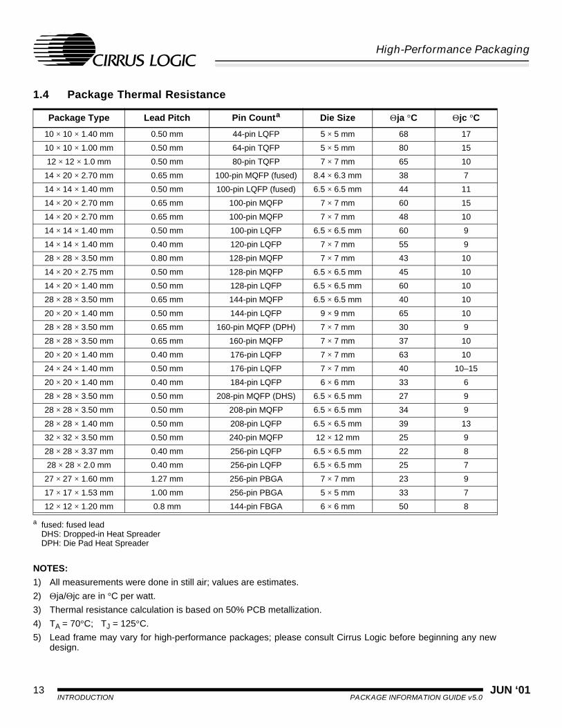
1.4 Package Thermal Resistance
NOTES:
1) All measurements were done in still air; values are estimates.
2) Θja/Θjc are in °C per watt.
3) Thermal resistance calculation is based on 50% PCB metallization.
4) TA = 70°C; TJ = 125°C.
5) Lead frame may vary for high-performance packages; please consult Cirrus Logic before beginning any newdesign.
Package Type Lead Pitch Pin Counta
a fused: fused leadDHS: Dropped-in Heat SpreaderDPH: Die Pad Heat Spreader
Die Size Θja °C Θjc °C
10 × 10 × 1.40 mm 0.50 mm 44-pin LQFP 5 × 5 mm 68 17
10 × 10 × 1.00 mm 0.50 mm 64-pin TQFP 5 × 5 mm 80 15
12 × 12 × 1.0 mm 0.50 mm 80-pin TQFP 7 × 7 mm 65 10
14 × 20 × 2.70 mm 0.65 mm 100-pin MQFP (fused) 8.4 × 6.3 mm 38 7
14 × 14 × 1.40 mm 0.50 mm 100-pin LQFP (fused) 6.5 × 6.5 mm 44 11
14 × 20 × 2.70 mm 0.65 mm 100-pin MQFP 7 × 7 mm 60 15
14 × 20 × 2.70 mm 0.65 mm 100-pin MQFP 7 × 7 mm 48 10
14 × 14 × 1.40 mm 0.50 mm 100-pin LQFP 6.5 × 6.5 mm 60 9
14 × 14 × 1.40 mm 0.40 mm 120-pin LQFP 7 × 7 mm 55 9
28 × 28 × 3.50 mm 0.80 mm 128-pin MQFP 7 × 7 mm 43 10
14 × 20 × 2.75 mm 0.50 mm 128-pin MQFP 6.5 × 6.5 mm 45 10
14 × 20 × 1.40 mm 0.50 mm 128-pin LQFP 6.5 × 6.5 mm 60 10
28 × 28 × 3.50 mm 0.65 mm 144-pin MQFP 6.5 × 6.5 mm 40 10
20 × 20 × 1.40 mm 0.50 mm 144-pin LQFP 9 × 9 mm 65 10
28 × 28 × 3.50 mm 0.65 mm 160-pin MQFP (DPH) 7 × 7 mm 30 9
28 × 28 × 3.50 mm 0.65 mm 160-pin MQFP 7 × 7 mm 37 10
20 × 20 × 1.40 mm 0.40 mm 176-pin LQFP 7 × 7 mm 63 10
24 × 24 × 1.40 mm 0.50 mm 176-pin LQFP 7 × 7 mm 40 10–15
20 × 20 × 1.40 mm 0.40 mm 184-pin LQFP 6 × 6 mm 33 6
28 × 28 × 3.50 mm 0.50 mm 208-pin MQFP (DHS) 6.5 × 6.5 mm 27 9
28 × 28 × 3.50 mm 0.50 mm 208-pin MQFP 6.5 × 6.5 mm 34 9
28 × 28 × 1.40 mm 0.50 mm 208-pin LQFP 6.5 × 6.5 mm 39 13
32 × 32 × 3.50 mm 0.50 mm 240-pin MQFP 12 × 12 mm 25 9
28 × 28 × 3.37 mm 0.40 mm 256-pin LQFP 6.5 × 6.5 mm 22 8
28 × 28 × 2.0 mm 0.40 mm 256-pin LQFP 6.5 × 6.5 mm 25 7
27 × 27 × 1.60 mm 1.27 mm 256-pin PBGA 7 × 7 mm 23 9
17 × 17 × 1.53 mm 1.00 mm 256-pin PBGA 5 × 5 mm 33 7
12 × 12 × 1.20 mm 0.8 mm 144-pin FBGA 6 × 6 mm 50 8

JUN ‘01 14PACKAGE INFORMATION GUIDE v5.0 INTRODUCTION
High-Performance Packaging
1.5 Package Electrical Characteristics
NOTES:
1) Loading capacitance measured using SEMI Method G-25-89.
2) Inductance measured using SEMI Method G-23-89.
3) Resistance measured using SEMI Method G-24-89.
Package Type Lead Pitch Pin Count a
a fused: fused leadDHS: Dropped-in Heat SpreaderDPH: Die Pad Heat Spreader
C (pF) L (nH) R (mΩ)
12 × 12 × 1.0 mm 0.50 mm 80-pin TQFP <2.0 3–5 <100
14 × 20 × 2.75 mm 0.65 mm 100-pin MQFP (fused) 2.0–3.0 3–6 <50
14 × 14 × 1.40 mm 0.50 mm 100-pin LQFP (fused) <2.0 3–6 <100
14 × 20 × 2.75 mm 0.65 mm 100-pin MQFP 2.0–3.0 5–15 75–250
14 × 20 × 2.75 mm 0.65 mm 100-pin MQFP 2.0–3.0 4–7 <50
14 × 14 × 1.40 mm 0.50 mm 100-pin LQFP <2.0 5–10 <100
14 × 14 × 1.40 mm 0.40 mm 120-pin LQFP <2.0 5–10 <100
28 × 28 × 3.50 mm 0.80 mm 128-pin MQFP 2.0–5.0 10–15 <75
14 × 20 × 2.75 mm 0.50 mm 128-pin MQFP 2.0–3.0 5–7 <50
14 × 14 × 1.40 mm 0.40 mm 128-pin LQFP <2.0 5–10 <100
28 × 28 × 3.50 mm 0.65 mm 144-pin MQFP 2.0–5.0 10–18 <75
20 × 20 × 1.40 mm 0.50 mm 144-pin LQFP 2.0–7.0 7–10 <100
28 × 28 × 3.50 mm 0.65 mm 160-pin MQFP (DPH) 3.0–6.0 10–15 <100
28 × 28 × 3.50 mm 0.65 mm 160-pin MQFP 2.0–5.0 11–19 <100
20 × 20 × 1.40 mm 0.40 mm 176-pin LQFP 2.0–7.0 7–10 <100
24 × 24 × 1.40 mm 0.50 mm 176-pin LQFP 2.0–10.0 8–11 <75
20 × 20 × 1.40 mm 0.40 mm 184-pin LQFP 2.0–10.0 8–11 <75
28 × 28 × 3.50 mm 0.50 mm 208-pin MQFP (DHS) 3.0–6.0 10–15 <125
28 × 28 × 3.50 mm 0.50 mm 208-pin MQFP 2.0–5.0 12–20 <125
28 × 28 × 1.40 mm 0.50 mm 208-pin LQFP <2.0 8–12 <50
32 × 32 × 3.50 mm 0.50 mm 240-pin MQFP <1.5 10–12 <50
28 × 28 × 3.37 mm 0.40 mm 256-pin MQFP <2.0 10–18 <80
28 × 28 × 2.0 mm 0.40 mm 256-pin LQFP <2.0 8–10 <100
27 × 27 × 2.33 mm 1.27 mm 256-pin PBGA <2.0 5–10 <25
17 × 17 × 1.53 mm 1.00 mm 256-pin PBGA <1.4 2–4 <20
12 × 12 × 1.20 mm 0.80 mm 144-pin FBGA <1.4 2–4 <20

JUN ‘0115PACKAGE OUTLINE DRAWINGS
High-Performance Packaging
PACKAGE INFORMATION GUIDE v5.0
2. PACKAGE OUTLINE DRAWINGS
2.1 20-, 28-, 44-, 68-, and 84-Pin PLCC
(This drawing refers to dimensions in Table 2-1 on page 16.)
EE1
0.042
0.048
D1
D
0.026
0.0320.050 A1
A
T
0.013
0.021
D3
E3
D2
E2
0.042
0.056
See Detail‘A’
0.013
0.0180.026
0.032
0.025
0.045R
0.020 MIN
DETAIL ‘A’
SEATING PLANEBASE PLANE

JUN ‘01 16PACKAGE INFORMATION GUIDE v5.0 PACKAGE OUTLINE DRAWINGS
High-Performance Packaging
NOTES:
1) Refer to JEDEC Publication 95, 1993 for symbol descriptions.
2) All dimensions are in inches, and controlling dimension is inch.
3) D1 and E1 do not include mold flash, which is 0.010 inch maximum.
4) D2/E2 will be determined at the seating plane.
5) Copper lead frame and lead finish is solder plate or matte-tin plate.
6) Formed leads are planar within 0.004 inch with respect to one another.
7) The top-half of the package above the lead frame can be smaller than the bottom-half of the package by amaximum of 0.010 inch.
Table 2-1. 20-, 28-, 44-, 68-, and 84-Pin PLCC Package Dimensions
Number of Pins
20 28 44 68 84
MIN MAX MIN MAX MIN MAX MIN MAX MIN MAX
A 0.165 0.180 0.165 0.180 0.165 0.180 0.165 0.200 0.165 0.200
A1 0.090 0.120 0.090 0.120 0.090 0.120 0.090 0.130 0.090 0.130
D 0.385 0.395 0.485 0.495 0.685 0.695 0.985 0.995 1.185 1.195
D1 0.350 0.356 0.450 0.456 0.650 0.656 0.950 0.958 1.150 1.158
D2 0.290 0.330 0.390 0.430 0.590 0.630 0.890 0.930 1.090 1.130
D3 0.200 REF 0.300 REF 0.500 REF 0.800 REF 1.000 REF
E 0.385 0.395 0.485 0.495 0.685 0.695 0.985 0.995 1.185 1.195
E1 0.350 0.356 0.450 0.456 0.650 0.656 0.950 0.958 1.150 1.158
E2 0.290 0.330 0.390 0.430 0.590 0.630 0.890 0.930 1.090 1.130
E3 0.200 REF 0.300 REF 0.500 REF 0.800 REF 1.000 REF
T 0.007 0.013 0.0077 0.0103 0.0077 0.0103 0.0077 0.0103 0.0077 0.0103

JUN ‘0117PACKAGE OUTLINE DRAWINGS
High-Performance Packaging
PACKAGE INFORMATION GUIDE v5.0
2.2 32-Pin LQFP
INCHES MILLIMETERSDIM MIN NOM MAX MIN NOM MAX
A --- 0.055 0.063 --- 1.40 1.60A1 0.002 0.004 0.006 0.05 0.10 0.15B 0.012 0.014 0.018 0.30 0.35 0.45D 0.343 0.354 0.366 8.70 9.0 BSC 9.30D1 0.272 0.28 0.280 6.90 7.0 BSC 7.10E 0.343 0.354 0.366 8.70 9.0 BSC 9.30
E1 0.272 0.28 0.280 6.90 7.0 BSC 7.10e* 0.028 0.31 BSC 0.035 0.70 0.80 BSC 0.90L 0.018 0.024 0.030 0.45 0.60 0.75∝ 0.000° 4° 7.000° 0.00° 4° 7.00°
* Nominal pin pitch is 0.50 mm
Controlling dimension is mm.JEDEC Designation: MS-022
E1
E
D1D
1
e
L
∝
B
A1
A
JUN ‘01 18PACKAGE INFORMATION GUIDE v5.0 PACKAGE OUTLINE DRAWINGS
High-Performance Packaging
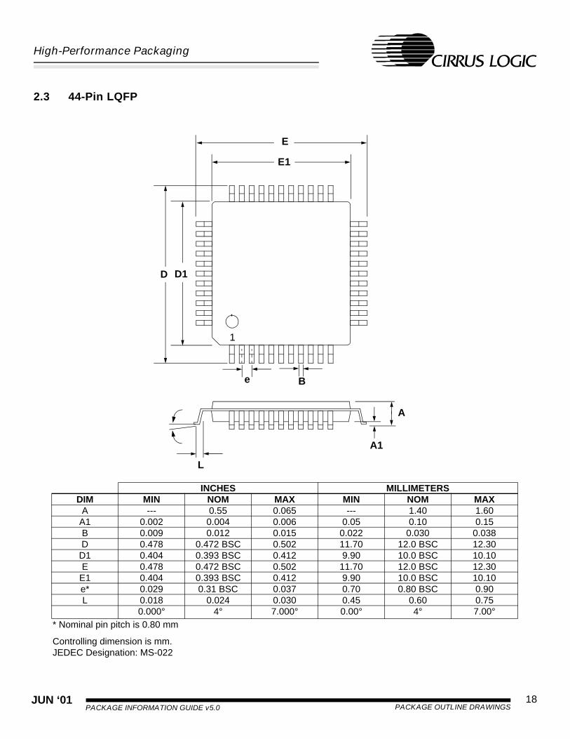
2.3 44-Pin LQFP
INCHES MILLIMETERSDIM MIN NOM MAX MIN NOM MAX
A --- 0.55 0.065 --- 1.40 1.60A1 0.002 0.004 0.006 0.05 0.10 0.15B 0.009 0.012 0.015 0.022 0.030 0.038D 0.478 0.472 BSC 0.502 11.70 12.0 BSC 12.30D1 0.404 0.393 BSC 0.412 9.90 10.0 BSC 10.10E 0.478 0.472 BSC 0.502 11.70 12.0 BSC 12.30
E1 0.404 0.393 BSC 0.412 9.90 10.0 BSC 10.10e* 0.029 0.31 BSC 0.037 0.70 0.80 BSC 0.90L 0.018 0.024 0.030 0.45 0.60 0.75∝ 0.000° 4° 7.000° 0.00° 4° 7.00°
* Nominal pin pitch is 0.80 mm
Controlling dimension is mm.JEDEC Designation: MS-022
E1
E
D1D
1
e
L
∝
B
A1
A

JUN ‘0119PACKAGE OUTLINE DRAWINGS
High-Performance Packaging
PACKAGE INFORMATION GUIDE v5.0
2.4 48-Pin LQFP
INCHES MILLIMETERSDIM MIN NOM MAX MIN NOM MAX
A --- 0.055 0.063 --- 1.40 1.60A1 0.002 0.004 0.006 0.05 0.10 0.15B 0.007 0.009 0.011 0.17 0.22 0.27D 0.343 0.354 0.366 8.70 9.0 BSC 9.30D1 0.272 0.28 0.280 6.90 7.0 BSC 7.10E 0.343 0.354 0.366 8.70 9.0 BSC 9.30
E1 0.272 0.28 0.280 6.90 7.0 BSC 7.10e* 0.016 0.020 0.024 0.40 0.50 BSC 0.60L 0.018 0.24 0.030 0.45 0.60 0.75∝ 0.000° 4° 7.000° 0.00° 4° 7.00°
* Nominal pin pitch is 0.50 mm
Controlling dimension is mm.JEDEC Designation: MS022
E1
E
D1D
1
e
L
∝
B
A1
A

JUN ‘01 20PACKAGE INFORMATION GUIDE v5.0 PACKAGE OUTLINE DRAWINGS
High-Performance Packaging
2.5 64-Pin LQFP
INCHES MILLIMETERSDIM MIN NOM MAX MIN NOM MAX
A --- 0.55 0.063 --- 1.40 1.60A1 0.002 0.004 0.006 0.05 0.10 0.15B 0.007 0.008 0.011 0.17 0.20 0.27D 0.461 0.472 BSC 0.484 11.70 12.0 BSC 12.30D1 0.390 0.393 BSC 0.398 9.90 10.0 BSC 10.10E 0.461 0.472 BSC 0.484 11.70 12.0 BSC 12.30
E1 0.390 0.393 BSC 0.398 9.90 10.0 BSC 10.10e* 0.016 0.020 BSC 0.024 0.40 0.50 BSC 0.60L 0.018 0.024 0.030 0.45 0.60 0.75∝ 0.000° 4° 7.000° 0.00° 4° 7.00°
* Nominal pin pitch is 0.50 mm
Controlling dimension is mm.JEDEC Designation: MS022
E1E
D1D
1
e
L
∝
B
A1
A

JUN ‘0121PACKAGE OUTLINE DRAWINGS
High-Performance Packaging
PACKAGE INFORMATION GUIDE v5.0
2.6 80-Pin TQFP (12 × 12 × 1.00-mm Body)
NOTES:
1) Dimensions are in millimeters, and controlling dimension is millimeter.
2) Package body dimensions do not include mold protrusion, which is 0.25 mm.
3) Pin 1 identification may be either ink dot or dimple.
4) The ‘lead width with plating’ dimension does not include a total allowable dambar protrusion of 0.08 mm (atmaximum material condition).
5) Ejector pin marks in molding are present on every package.
Pin 1 Indicator
Pin 1
14.00 (0.551)
0.17 (0.007)
12.00 (0.472)
BSC
14.00 (0.551)
12.00 (0.472)
0.95 (0.037)
0° MIN7° MAX0.09 (0.004)
1.20 (0.047)
0.45 (0.018)
0.05 (0.002)
Pin 80
1.00 (0.039)
0.50
BSC
BSC
0.27 (0.011)
BSC
(0.020)
BSC
0.75 (0.030)
REF1.05 (0.041)
0.20 (0.008)
MAX 0.15 (0.006)
JUN ‘01 22PACKAGE INFORMATION GUIDE v5.0 PACKAGE OUTLINE DRAWINGS
High-Performance Packaging
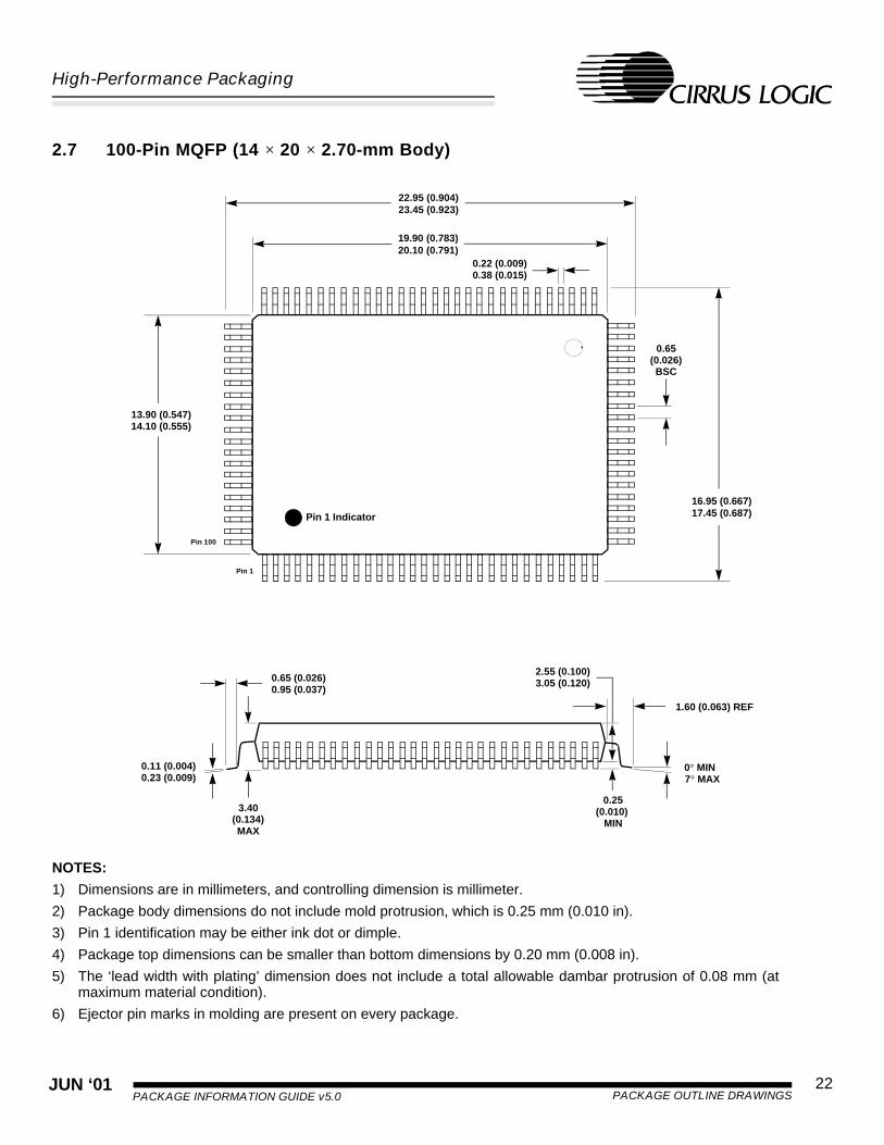
2.7 100-Pin MQFP (14 × 20 × 2.70-mm Body)
NOTES:
1) Dimensions are in millimeters, and controlling dimension is millimeter.
2) Package body dimensions do not include mold protrusion, which is 0.25 mm (0.010 in).
3) Pin 1 identification may be either ink dot or dimple.
4) Package top dimensions can be smaller than bottom dimensions by 0.20 mm (0.008 in).
5) The ‘lead width with plating’ dimension does not include a total allowable dambar protrusion of 0.08 mm (atmaximum material condition).
6) Ejector pin marks in molding are present on every package.
Pin 1 Indicator
Pin 1
19.90 (0.783)
22.95 (0.904)23.45 (0.923)
20.10 (0.791)
16.95 (0.667)17.45 (0.687)
13.90 (0.547)14.10 (0.555)
0.11 (0.004)0.23 (0.009)
1.60 (0.063) REF
2.55 (0.100)3.05 (0.120)0.65 (0.026)
0.95 (0.037)
0° MIN7° MAX
0.22 (0.009)0.38 (0.015)
0.65(0.026)BSC
Pin 100
3.400.25
(0.134)MAX
(0.010) MIN

JUN ‘0123PACKAGE OUTLINE DRAWINGS
High-Performance Packaging
PACKAGE INFORMATION GUIDE v5.0
2.8 100-Pin LQFP (14 × 14 × 1.40-mm Body)
NOTES:
1) Dimensions are in millimeters (inches), and controlling dimension is millimeter.
2) Package body dimensions do not include mold protrusion, which is 0.25 mm (0.010 in).
3) Pin 1 identification may be either ink dot or dimple.
4) Package top dimensions can be smaller than bottom dimensions by 0.20 mm (0.008 in).
5) The ‘lead width with plating’ dimension does not include a total allowable dambar protrusion of 0.08 mm (atmaximum material condition).
6) Ejector pin marks in molding are present on every package.
Pin 1 Indicator
12.00 (0.472) REF
Pin 1
15.56 (0.613)16.50 (0.650)
0.08 (0.003)0.28 (0.011)
13.90 (0.547)14.10 (0.555)
12.00(0.472)
REF
0.50(0.0197)
BSC
15.56 (0.613)16.50 (0.650)
13.90 (0.547)14.10 (0.555)
1.25 (0.049)1.50 (0.059)
0° MIN7° MAX
0.08 (0.003)0.23 (0.009)
1.40 (0.055)1.65 (0.065)
0.30 (0.012)0.70 (0.028)
0.05 (0.002)0.15 (0.006)
Pin 100
1.00(0.039)
REF

JUN ‘01 24PACKAGE INFORMATION GUIDE v5.0 PACKAGE OUTLINE DRAWINGS
High-Performance Packaging
2.9 120-Pin LQFP (14 × 14 × 1.40-mm Body)
NOTES:
1) Dimensions are in millimeters (inches), and controlling dimension is millimeter.
2) Package body dimensions do not include mold protrusion, which is 0.25 mm (0.010 in).
3) Pin 1 identification may be either ink dot or dimple.
4) Package top dimensions can be smaller than bottom dimensions by 0.20 mm (0.008 in).
5) The ‘lead width with plating’ dimension does not include a total allowable dambar protrusion of 0.08 mm (atmaximum material condition).
6) Ejector pin marks in molding are present on every package.
Pin 1 Indicator
11.60 (0.457) REF
Pin 1
15.56 (0.613)16.50 (0.650)
0.09 (0.004)0.21 (0.008)
13.90 (0.547)14.10 (0.555)
11.60(0.457)
REF
0.40(0.0157)
BSC
15.56 (0.613)16.50 (0.650)
13.90 (0.547)14.10 (0.555)
1.25 (0.049)1.50 (0.059)
0° MIN7° MAX
0.07 (0.003)0.17 (0.007)
1.40 (0.055)1.65 (0.065)
0.30 (0.012)0.70 (0.028)
0.05 (0.002)0.15 (0.006)
Pin 120
1.00(0.039)
REF

JUN ‘0125PACKAGE OUTLINE DRAWINGS
High-Performance Packaging
PACKAGE INFORMATION GUIDE v5.0
2.10 128-Pin MQFP (28 × 28 × 3.50-mm Body)
NOTES:
1) Dimensions are in millimeters (inches), and controlling dimension is millimeter.
2) Package body dimensions do not include mold protrusion, which is 0.25 mm (0.010 in).
3) Pin 1 identification may be either ink dot or dimple.
4) Package top dimensions can be smaller than bottom dimensions by 0.20 mm (0.008 in).
5) The ‘lead width with plating’ dimension does not include a total allowable dambar protrusion of 0.08 mm (atmaximum material condition).
6) Ejector pin marks in molding are present on every package.
Pin 1 Indicator
31.65 (1.246)32.15 (1.266)
0.30 (0.012)0.45 (0.018)
27.90 (1.098)28.10 (1.106)
0.80(0.031)BSC
31.65 (1.246)32.15 (1.266)
27.90 (1.098)28.10 (1.106)
3.17 (0.125)3.67 (0.144)
0° MIN7° MAX
0.11 (0.004)0.23 (0.009)
4.07
0.65 (0.026)0.95 (0.037)
0.25
1.60 (0.063)
Pin 1
Pin 128
(0.160)MAX
(0.010)MIN
REF

JUN ‘01 26PACKAGE INFORMATION GUIDE v5.0 PACKAGE OUTLINE DRAWINGS
High-Performance Packaging
2.11 128-Pin MQFP (14 × 20 × 2.70-mm Body)
NOTES:
1) Dimensions are in millimeters (inches), and controlling dimension is millimeter.
2) Package body dimensions do not include mold protrusion, which is 0.25 mm (0.010 in).
3) Pin 1 identification may be either ink dot or dimple.
4) Package top dimensions can be smaller than bottom dimensions by 0.20 mm (0.008 in).
5) The ‘lead width with plating’ dimension does not include a total allowable dambar protrusion of 0.08 mm (atmaximum material condition).
6) Ejector pin marks in molding are present on every package.
Pin 1 Indicator
19.90 (0.783)
23.65 (0.931)24.15 (0.951)
20.10 (0.791)0.22 (0.009)0.38 (0.015)
17.65 (0.695)18.15 (0.715)
13.90 (0.547)14.10 (0.555)
Pin 1
0.50(0.020)BSC
1.60 (0.063)
3.40
0° MIN7° MAX
0.13 (0.005)0.23 (0.009)
0.65 (0.026)0.95 (0.037)
2.55 (0.100)3.05 (0.120)
0.25
Pin 128
(0.134)MAX
(0.010)MIN
REF

JUN ‘0127PACKAGE OUTLINE DRAWINGS
High-Performance Packaging
PACKAGE INFORMATION GUIDE v5.0
2.12 128-Pin LQFP (14 × 14 × 1.40-mm Body)
NOTES:
1) Dimensions are in millimeters (inches), and controlling dimension is millimeter.
2) Package body dimensions do not include mold protrusion, which is 0.25 mm (0.010 in).
3) Pin 1 identification may be either ink dot or dimple.
4) Package top dimensions can be smaller than bottom dimensions by 0.20 mm (0.008 in).
5) The ‘lead width with plating’ dimension does not include a total allowable dambar protrusion of 0.08 mm (atmaximum material condition).
6) Ejector pin marks in molding are present on every package.
Pin 1 Indicator
Pin 1
0.13 (0.005)0.23 (0.009)
14.00 (0.551)
0.40(0.0157)
16.00
14.00
1.35 (0.053)1.45 (0.057)
0° MIN7° MAX
0.09 (0.004)0.20 (0.008)
1.40 (0.055)1.60 (0.063)
0.45 (0.018)0.75 (0.030)
0.05 (0.002)0.15 (0.006)
Pin 128
1.00(0.039)
REF
(0.630)
(0.551)
16.00 (0.630)
JUN ‘01 28PACKAGE INFORMATION GUIDE v5.0 PACKAGE OUTLINE DRAWINGS
High-Performance Packaging
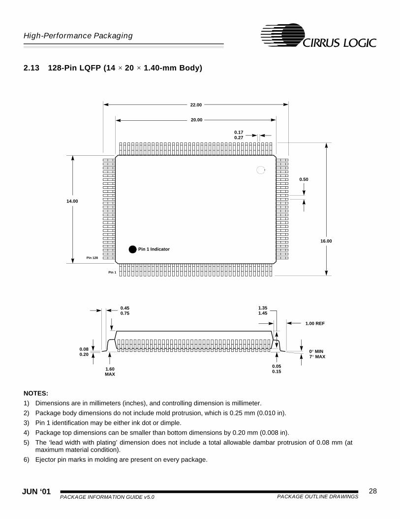
2.13 128-Pin LQFP (14 × 20 × 1.40-mm Body)
NOTES:
1) Dimensions are in millimeters (inches), and controlling dimension is millimeter.
2) Package body dimensions do not include mold protrusion, which is 0.25 mm (0.010 in).
3) Pin 1 identification may be either ink dot or dimple.
4) Package top dimensions can be smaller than bottom dimensions by 0.20 mm (0.008 in).
5) The ‘lead width with plating’ dimension does not include a total allowable dambar protrusion of 0.08 mm (atmaximum material condition).
6) Ejector pin marks in molding are present on every package.
Pin 1 Indicator
20.00
22.00
0.170.27
16.00
14.00
Pin 1
0.50
1.00 REF
1.60
0° MIN7° MAX
0.080.20
0.450.75
1.351.45
0.05
Pin 128
MAX0.15

JUN ‘0129PACKAGE OUTLINE DRAWINGS
High-Performance Packaging
PACKAGE INFORMATION GUIDE v5.0
2.14 144-Pin MQFP (28 × 28 × 3.50-mm Body)
NOTES:
1) Dimensions are in millimeters (inches), and controlling dimension is millimeter.
2) Package body dimensions do not include mold protrusion, which is 0.25 mm (0.010 in).
3) Pin 1 identification may be either ink dot or dimple.
4) Package top dimensions can be smaller than bottom dimensions by 0.20 mm (0.008 in).
5) The ‘lead width with plating’ dimension does not include a total allowable dambar protrusion of 0.08 mm (atmaximum material condition).
6) Ejector pin marks in molding are present on every package.
7) Drawing above does not reflect exact package pin count.
Pin 1 Indicator
22.75 (0.896) REF
30.95 (1.219)31.45 (1.238)
0.22 (0.009)0.38 (0.015)
27.90 (1.098)28.10 (1.106)
22.75(0.896)
REF
0.65(0.0256)
BSC
30.95 (1.219)31.45 (1.238)
27.90 (1.098)28.10 (1.106)
3.17 (0.125)3.67 (0.144)
0° MIN7° MAX
0.13 (0.005)0.23 (0.009) 4.07
0.65 (0.026)0.95 (0.037)
0.25
1.60 (0.063) REF
Pin 1
Pin 144
(0.160)MAX
(0.010)MIN

JUN ‘01 30PACKAGE INFORMATION GUIDE v5.0 PACKAGE OUTLINE DRAWINGS
High-Performance Packaging
2.15 144-Pin LQFP (20 × 20 × 1.40-mm Body)
NOTES:
1) Dimensions are in millimeters (inches), and controlling dimension is millimeter.
2) Package body dimensions do not include mold protrusion, which is 0.25 mm (0.010 in).
3) Pin 1 identification may be either ink dot or dimple.
4) Package top dimensions can be smaller than bottom dimensions by 0.20 mm (0.008 in).
5) The ‘lead width with plating’ dimension does not include a total allowable dambar protrusion of 0.08 mm (atmaximum material condition).
6) Ejector pin marks in molding are present on every package.
Pin 1 Indicator
Pin 1
22.00 (0.866)BSC
0.17 (0.007)0.27 (0.011)
20.00 (0.787)BSC
0.50(0.020)BSC
1.35 (0.053)1.45 (0.057)
0° MIN7° MAX
0.09 (0.004)0.20 (0.008)
1.60 (0.063)MAX
0.45 (0.018)0.75 (0.030)
22.00 (0.866)BSC
20.00 (0.787)BSC
1.00(0.039)
REF
0.05 (0.002)0.15 (0.006)
Pin 144

JUN ‘0131PACKAGE OUTLINE DRAWINGS
High-Performance Packaging
PACKAGE INFORMATION GUIDE v5.0
2.16 160-Pin MQFP (28 × 28 × 3.50-mm Body)
NOTES:1) Dimensions are in millimeters (inches), and controlling dimension is millimeter.2) Package body dimensions do not include mold protrusion, which is 0.25 mm (0.010 in).3) Pin 1 identification may be either ink dot or dimple.4) Package top dimensions can be smaller than bottom dimensions by 0.20 mm (0.008 in).5) The ‘lead width with plating’ dimension does not include a total allowable dambar protrusion of 0.08 mm (at
maximum material condition).6) Ejector pin marks in molding are present on every package.7) Drawing above does not reflect exact package pin count.
4.07
Pin 1 Indicator
25.35 (0.998) REF
30.95 (1.219)31.45 (1.238)
0.22 (0.009)0.38 (0.015)
27.90 (1.098)28.10 (1.106)
25.35(0.998)
REF
0.65(0.0256)
BSC
30.95 (1.219)31.45 (1.238)
27.90 (1.098)28.10 (1.106)
3.17 (0.125)3.67 (0.144)
0° MIN7° MAX
0.65 (0.026)0.95 (0.037)
0.25
1.60 (0.063) REF
Pin 1
Pin 160
0.13 (0.005)0.23 (0.009)
(0.160) (0.010)MINMAX

JUN ‘01 32PACKAGE INFORMATION GUIDE v5.0 PACKAGE OUTLINE DRAWINGS
High-Performance Packaging
2.17 176-Pin LQFP (20 × 20 × 1.40-mm Body)
NOTES:
1) Dimensions are in millimeters (inches), and controlling dimension is millimeter.
2) Package body dimensions do not include mold protrusion, which is 0.25 mm (0.010 in).
3) Pin 1 identification may be either ink dot or dimple.
4) Package top dimensions can be smaller than bottom dimensions by 0.20 mm (0.008 in).
5) The ‘lead width with plating’ dimension does not include a total allowable dambar protrusion of 0.08 mm (atmaximum material condition).
6) Ejector pin marks in molding are present on every package.
7) Drawing does not reflect the exact package pin count.
Pin 1 Indicator
17.20 (0.677) REF
Pin 1
21.90 (0.862)22.10 (0.870)
0.13 (0.005)0.23 (0.009)
19.90 (0.783)20.10 (0.791)
17.20
REF0.40
BSC
1.35 (0.053)1.45 (0.057)
0° MIN7° MAX
0.09 (0.004)0.20 (0.008)
1.40 (0.055)1.60 (0.063)
0.45 (0.018)0.75 (0.030)
21.90 (0.862)22.10 (0.870)
19.90 (0.783)20.10 (0.791)
1.00(0.039)
REF
0.05 (0.002)0.15 (0.006)
Pin 176
(0.0157)(0.677)

JUN ‘0133PACKAGE OUTLINE DRAWINGS
High-Performance Packaging
PACKAGE INFORMATION GUIDE v5.0
2.18 176-Pin LQFP (24 × 24 × 1.40-mm Body)
NOTES:
1) Dimensions are in millimeters (inches), and controlling dimension is millimeter.
2) Package body dimensions do not include mold protrusion, which is 0.25 mm (0.010 in).
3) Pin 1 identification may be either ink dot or dimple.
4) Package top dimensions can be smaller than bottom dimensions by 0.20 mm (0.008 in).
5) The ‘lead width with plating’ dimension does not include a total allowable dambar protrusion of 0.08 mm (atmaximum material condition).
6) Ejector pin marks in molding are present on every package.
7) Drawing does not reflect the exact package pin count.
Pin 1 Indicator
0.17 (0.007)0.27 (0.011)
24.00 (0.948)
0.50(0.020)
1.35 (0.053)1.45 (0.057)
0° MIN7° MAX
0.45 (0.018)0.75 (0.030)
Pin 1
Pin 176
0.09 (0.004)0.20 (0.008)
0.05 (0.002)1.60 (0.063)
MAX
1.00 (0.039)REF
24.00
26.00 (1.024)
26.00
(0.948)
(1.024)
0.15 (0.006)

JUN ‘01 34PACKAGE INFORMATION GUIDE v5.0 PACKAGE OUTLINE DRAWINGS
High-Performance Packaging
2.19 184-Pin LQFP (20 × 20 × 1.40-mm Body)
NOTES:1) Dimensions are in millimeters, and controlling dimension is millimeter.
2) Package body dimensions do not include mold protrusion, which is 0.25 mm (0.010 in).
3) Pin 1 identification may be either ink dot or dimple.
4) Package top dimensions can be smaller than bottom dimensions by 0.20 mm (0.008 in).
5) The ‘lead width with plating’ dimension does not include a total allowable dambar protrusion of 0.08 mm (atmaximum material condition).
6) Ejector pin marks in molding are present on every package.
7) Drawing above does not reflect exact package pin count.
Pin 1 Indicator
0.13 MIN0.23 MAX
19.90 MIN
0.40BSC
1.35 MIN1.45 MAX
3° MIN7° MAX
0.45 MIN0.75 MAX
Pin 1
Pin 184
0.13 MIN0.23 MAX
0.05 MIN1.60 MAX
0.90 MIN1.10 MAX
19.90 MIN
21.80 MIN
21.80 MIN
20.10 MAX
22.20 MAX
0.15 MAX
22.20 MAX
20.10 MAX

JUN ‘0135PACKAGE OUTLINE DRAWINGS
High-Performance Packaging
PACKAGE INFORMATION GUIDE v5.0
2.20 208-Pin MQFP (28 × 28 × 3.50-mm Body)
NOTES:1) Dimensions are in millimeters (inches), and controlling dimension is millimeter.2) Package body dimensions do not include mold protrusion, which is 0.25 mm (0.010 in).3) Pin 1 identification may be either ink dot or dimple.4) Package top dimensions can be smaller than bottom dimensions by 0.20 mm (0.008 in).5) The ‘lead width with plating’ dimension does not include a total allowable dambar protrusion of 0.08 mm (at
maximum material condition).6) Ejector pin marks in molding are present on every package.7) Drawing above does not reflect exact package pin count.
Pin 1 Indicator
25.50 (1.004) REF
30.35 (1.195)30.85 (1.215)
0.13 (0.005)0.28 (0.011)
27.90 (1.098)28.10 (1.106)
25.50(1.004)
REF
0.50(0.0197)
BSC
30.35 (1.195)30.85 (1.215)
27.90 (1.098)28.10 (1.106)
3.17 (0.125)3.67 (0.144)
0° MIN7° MAX
0.09 (0.004)0.23 (0.009)
4.07
0.40 (0.016)0.75 (0.030)
0.25
1.30 (0.051) REF
Pin 1
Pin 208
(0.160)MAX
(0.010)MIN

JUN ‘01 36PACKAGE INFORMATION GUIDE v5.0 PACKAGE OUTLINE DRAWINGS
High-Performance Packaging
2.21 208-Pin LQFP (28 × 28 × 1.40-mm Body)
NOTES:1) Dimensions are in millimeters, and controlling dimension is millimeter.
2) Package body dimensions do not include mold protrusion, which is 0.25 mm (0.010 in).
3) Pin 1 identification may be either ink dot or dimple.
4) Package top dimensions can be smaller than bottom dimensions by 0.20 mm (0.008 in).
5) The ‘lead width with plating’ dimension does not include a total allowable dambar protrusion of 0.08 mm (atmaximum material condition).
6) Ejector pin marks in molding are present on every package.
7) Drawing above does not reflect exact package pin count.
Pin 1 Indicator
29.60 (1.165)30.40 (1.197)
0.17 (0.007)0.27 (0.011)
27.80 (1.094)28.20 (1.110)
0.50(0.0197)
BSC
29.60 (1.165)30.40 (1.197)
27.80 (1.094)28.20 (1.110)
1.35 (0.053)1.45 (0.057)
0° MIN7° MAX
0.09 (0.004)0.20 (0.008)
1.40 (0.055)
0.45 (0.018)0.75 (0.030)
0.05 (0.002)
1.00 (0.039) BSC
Pin 1
Pin 208
1.60 (0.063) 0.15 (0.006)
JUN ‘0137PACKAGE OUTLINE DRAWINGS
High-Performance Packaging
PACKAGE INFORMATION GUIDE v5.0
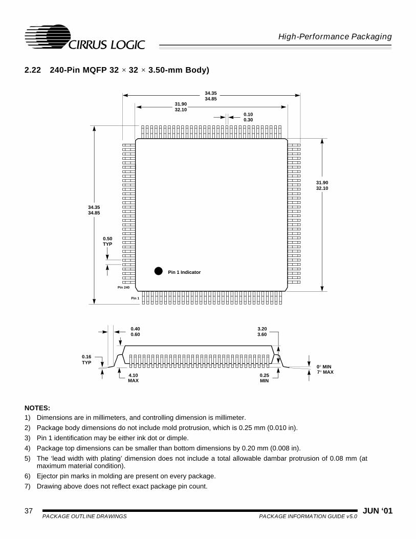
2.22 240-Pin MQFP 32 × 32 × 3.50-mm Body)
NOTES:1) Dimensions are in millimeters, and controlling dimension is millimeter.
2) Package body dimensions do not include mold protrusion, which is 0.25 mm (0.010 in).
3) Pin 1 identification may be either ink dot or dimple.
4) Package top dimensions can be smaller than bottom dimensions by 0.20 mm (0.008 in).
5) The ‘lead width with plating’ dimension does not include a total allowable dambar protrusion of 0.08 mm (atmaximum material condition).
6) Ejector pin marks in molding are present on every package.
7) Drawing above does not reflect exact package pin count.
3.203.60
0° MIN7° MAX
0.25MIN
Pin 1 Indicator
34.3534.85
0.100.30
31.9032.10
0.50TYP
34.3534.85
31.9032.10
0.16
4.10
0.400.60
Pin 1
Pin 240
MAX
TYP

JUN ‘01 38PACKAGE INFORMATION GUIDE v5.0 PACKAGE OUTLINE DRAWINGS
High-Performance Packaging
2.23 256-Pin MQFP (28 × 28 × 3.50-mm Body)
NOTES:
1) Dimensions are in millimeters, and controlling dimension is millimeter.
2) Package body dimensions do not include mold protrusion, which is 0.25 mm (0.010 in).
3) Pin 1 identification may be either ink dot or dimple.
4) Package top dimensions can be smaller than bottom dimensions by 0.20 mm (0.008 in).
5) The ‘lead width with plating’ dimension does not include a total allowable dambar protrusion of 0.08 mm (atmaximum material condition).
6) Ejector pin marks in molding are present on every package.
7) Drawing above does not reflect exact package pin count.
3.20
0° MIN7° MAX
0.25MIN
Pin 1 Indicator
30.60
0.13 0.23
28.00
0.40BSC
30.60
28.00
0.13
4.07
0.50
Pin 1
Pin 256
MAX
0.23
25.20REF
3.600.75
JUN ‘0139PACKAGE OUTLINE DRAWINGS
High-Performance Packaging
PACKAGE INFORMATION GUIDE v5.0
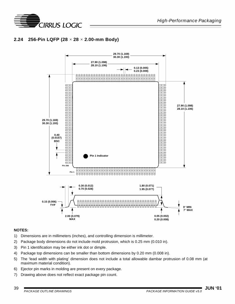
2.24 256-Pin LQFP (28 × 28 × 2.00-mm Body)
NOTES:
1) Dimensions are in millimeters (inches), and controlling dimension is millimeter.
2) Package body dimensions do not include mold protrusion, which is 0.25 mm (0.010 in).
3) Pin 1 identification may be either ink dot or dimple.
4) Package top dimensions can be smaller than bottom dimensions by 0.20 mm (0.008 in).
5) The ‘lead width with plating’ dimension does not include a total allowable dambar protrusion of 0.08 mm (atmaximum material condition).
6) Ejector pin marks in molding are present on every package.
7) Drawing above does not reflect exact package pin count.
1.80 (0.071)1.95 (0.077)
0° MIN7° MAX
0.05 (0.002)0.20 (0.008)
Pin 1 Indicator
29.70 (1.169)30.30 (1.193)
0.13 (0.005)0.23 (0.009)
27.90 (1.098)28.10 (1.106)
0.40(0.0157)
BSC
29.70 (1.169)30.30 (1.193)
27.90 (1.098)28.10 (1.106)
0.15 (0.006)
2.00 (0.079)
0.30 (0.012)0.70 (0.028)
Pin 1
Pin 256
MAX
TYP

JUN ‘01 40PACKAGE INFORMATION GUIDE v5.0 PACKAGE OUTLINE DRAWINGS
High-Performance Packaging
2.25 256-Pin PBGA (27 × 27 × 1.60-mm Body)
NOTES:
1) Dimensions are in millimeters (inches), and controlling dimension is millimeter.
2) Before beginning any new design with this device, please contact Cirrus Logic for the latest packageinformation.
TOP VIEW
26.80 (1.055)27.20 (1.071)
24.00 REF(0.945)
SIDE VIEW
BOTTOM VIEW
26.80 (1.055)27.20 (1.071)
26.80 (1.055)27.20 (1.071)
ABCDEFGHJKLMNPRTUVWY
1.27 (0.050)
1.44
1.27 (0.050)1.44 REF
0.30 (0.012)
26.80 (1.055)27.20 (1.071)
24.00 REF(0.945)
Pin 1 Indicator
Pin 1 Corner
(0.057)
BSC
REF
REF
(0.057)
Pin 1 Corner
20 19 18 17 16 15 14 13 12 11 10 9 8 7 6 5 4 3 2 1
BSC
2.12 (0.083)2.54 (0.100)
0.50 (0.020)0.70 (0.028)
0.56 (0.022)REF

JUN ‘0141PACKAGE OUTLINE DRAWINGS
High-Performance Packaging
PACKAGE INFORMATION GUIDE v5.0
2.26 256-Pin PBGA (17 × 17 × 1.53-mm Body)
NOTES:
1) Dimensions are in millimeters (inches), and controlling dimension is millimeter.
2) Before beginning any new design with this device, please contact Cirrus Logic for the latest packageinformation.
TOP VIEW
17.00 (0.669)
15.00 (0.590)
SIDE VIEW
BOTTOM VIEW
ABCDEFGHJKLMNPRT
1.00 (0.040)
Pin 1 Indicator
Pin 1 Corner
Pin 1 Corner
16 15 14 13 12 11 10 9 8 7 6 5 4 3 2 1
+0.70 (.027) -0.00
15.00 (0.590)+0.70 (.027) -0.00
4 Layer
2 Layer
17.00 (0.669)
17.00 (0.669)1.00 (0.040)
1.00 (0.040)
1.00 (0.040)
30° TYP
REF
REF
0.50
3 Places
0.80 (0.032)±0.05 (.002)
0.40 (0.016)±0.10 (.004)
0.56 (0.022)±0.06 (0.002)
0.36 (0.022)+0.04 (0.001)–0.06 (0.002)
17.00 (0.669)
R
JUN ‘01 42PACKAGE INFORMATION GUIDE v5.0 PACKAGE OUTLINE DRAWINGS
High-Performance Packaging
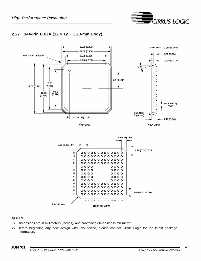
2.27 144-Pin FBGA (12 × 12 × 1.20-mm Body)
NOTES:
1) Dimensions are in millimeters (inches), and controlling dimension is millimeter.
2) Before beginning any new design with this device, please contact Cirrus Logic for the latest packageinformation.
TOP VIEW
12.00 (0.472)
SIDE VIEW
BOTTOM VIEW
N
M
L
K
J
H
G
F
E
D
C
B
A
1.20 (0.047) TYP
Ball 1 Pad Indicator
Pin 1 Corner
1 2 3 4 5 6 7 8 9 10 11 12 13
4.0 (0.157)
0.80 (0.031) TYP
11.60
4.0 (0.157)
(0.456)
10.05(0.395)
(0.376)9.55
0.25 Rad
1.20 (0.047) TYP
0.80 (0.031) TYP
1.17 (0.046)
0.48 (0.019)TYP
0.835 (0.033)
0.35 (0.014)
0.085 (0.003)12.00 (0.472)
11.60 (0.456)
10.05 (0.395)
9.55 (0.376)
(2 places)
30°

PACKAGE INFORMATION GUIDE v5.0JUN ‘0143
PACKAGE DRAWINGS – CRYSTAL SEMICONDUCTOR PRODUCTS DIVISION
High-Performance Packaging
3. PACKAGE DRAWINGS – CRYSTAL SEMICONDUCTOR PRODUCTS DIVISION
3.1 8-Pin PDIP (300 -mm Body)
INCHES MILLIMETERSDIM MIN NOM MAX MIN NOM MAX
A 0.150 0.175 0.200 3.81 4.45 5.08A1 0.015 0.028 0.040 0.38 0.71 1.02A2 0.115 0.138 0.160 2.92 3.51 4.06b 0.015 0.040 0.065 0.38 1.02 1.65b1 0.045 0.055 0.065 1.14 1.40 1.65c 0.008 0.012 0.015 0.20 0.30 0.38D 0.355 0.365 0.400 9.017 9.27 10.16E 0.300 BSC 7.62 BSCE1 0.240 0.25 0.260 6.10 6.35 6.60e 0.100 BSC 2.54 BSC
eB 0.330 0.35 0.370 8.38 8.89 9.40eC 0.015 0.025 0.035 .38 0.635 .89L 0.115 0.125 0.135 2.92 3.175 3.43∝ 0° 5° 10° 0° 5° 10°
JEDEC # : MS-001
Controling Dimension is Inches
E1
D
SEATINGPLANE
b1e
b
A
LA1
∝
TOP VIEW
BOTTOM VIEW SIDE VIEW
1
c
A2
EeC
eB

JUN ‘01 44PACKAGE INFORMATION GUIDE v5.0 PACKAGE DRAWINGS – CRYSTAL
SEMICONDUCTOR PRODUCTS DIVISION
High-Performance Packaging
3.2 14-Pin PDIP
DimensionInches Millimeters
MIN MAX MIN MAX
A 0.000 0.210 0.00 5.33
A1 0.015 0.025 0.38 0.64
A2 0.115 0.195 2.92 4.95
b 0.014 0.022 0.36 0.56
b1 0.045 0.070 1.14 1.78
c 0.008 0.014 0.20 0.36
D 0.735 0.775 18.67 19.69
E 0.300 0.325 7.62 8.26
E1 0.240 0.280 6.10 7.11
e 0.090 0.110 2.29 2.79
eA 0.280 0.320 7.11 8.13
eB 0.300 0.430 7.62 10.92
eC 0.000 0.060 0.00 1.52
L 0.115 0.150 2.92 3.81
µ 0° 15° 0° 15°
E1
D
SEATINGPLANE
b1e
b
A
LA1
µ
TOP VIEW
BOTTOM VIEW SIDE VIEW
1
eAc
A2
EeC
eB

PACKAGE INFORMATION GUIDE v5.0JUN ‘0145
PACKAGE DRAWINGS – CRYSTAL SEMICONDUCTOR PRODUCTS DIVISION
High-Performance Packaging
3.3 16-Pin PDIP
DimensionInches Millimeters
MIN MAX MIN MAX
A 0.000 0.210 0.00 5.33
A1 0.015 0.025 0.38 0.64
A2 0.115 0.195 2.92 4.95
b 0.014 0.022 0.36 0.56
b1 0.045 0.070 1.14 1.78
c 0.008 0.014 0.20 0.36
D 0.780 0.800 19.81 20.32
E 0.300 0.325 7.62 8.26
E1 0.240 0.280 6.10 7.11
e 0.090 0.110 2.29 2.79
eA 0.280 0.320 7.11 8.13
eB 0.300 0.430 7.62 10.92
eC 0.000 0.060 0.00 1.52
L 0.115 0.150 2.92 3.81
µ 0° 15° 0° 15°
E1
D
SEATINGPLANE
b1e
b
A
LA1
µ
TOP VIEW
BOTTOM VIEW SIDE VIEW
1
c
A2
EeC
eB
eA
JUN ‘01 46PACKAGE INFORMATION GUIDE v5.0 PACKAGE DRAWINGS – CRYSTAL
SEMICONDUCTOR PRODUCTS DIVISION
High-Performance Packaging
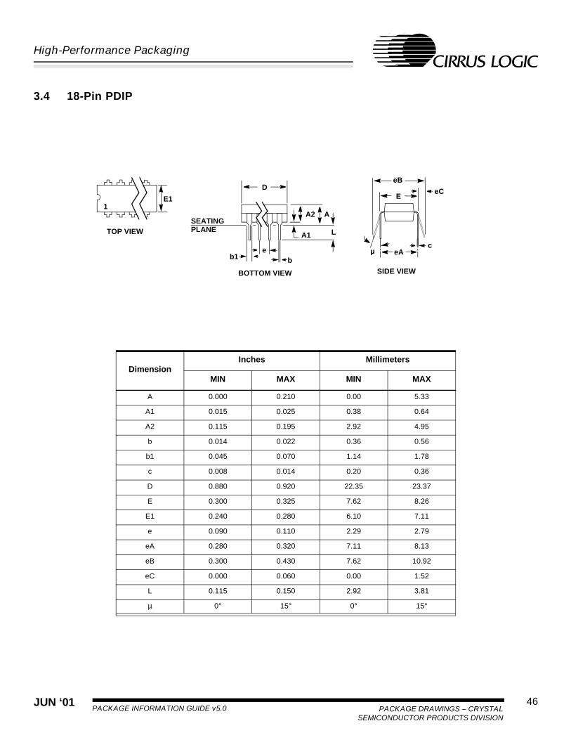
3.4 18-Pin PDIP
DimensionInches Millimeters
MIN MAX MIN MAX
A 0.000 0.210 0.00 5.33
A1 0.015 0.025 0.38 0.64
A2 0.115 0.195 2.92 4.95
b 0.014 0.022 0.36 0.56
b1 0.045 0.070 1.14 1.78
c 0.008 0.014 0.20 0.36
D 0.880 0.920 22.35 23.37
E 0.300 0.325 7.62 8.26
E1 0.240 0.280 6.10 7.11
e 0.090 0.110 2.29 2.79
eA 0.280 0.320 7.11 8.13
eB 0.300 0.430 7.62 10.92
eC 0.000 0.060 0.00 1.52
L 0.115 0.150 2.92 3.81
µ 0° 15° 0° 15°
E1
D
SEATINGPLANE
b1e
b
A
LA1
µ
TOP VIEW
BOTTOM VIEW SIDE VIEW
1
c
A2
EeC
eB
eA

PACKAGE INFORMATION GUIDE v5.0JUN ‘0147
PACKAGE DRAWINGS – CRYSTAL SEMICONDUCTOR PRODUCTS DIVISION
High-Performance Packaging
3.5 20-Pin PDIP
DimensionInches Millimeters
MIN MAX MIN MAX
A 0.000 0.210 0.00 5.33
A1 0.015 0.025 0.38 0.64
A2 0.115 0.195 2.92 4.95
b 0.014 0.022 0.36 0.56
b1 0.045 0.070 1.14 1.78
c 0.008 0.014 0.20 0.36
D 0.980 1.060 24.89 26.92
E 0.300 0.325 7.62 8.26
E1 0.240 0.280 6.10 7.11
e 0.090 0.110 2.29 2.79
eA 0.280 0.320 7.11 8.13
eB 0.300 0.430 7.62 10.92
eC 0.000 0.060 0.00 1.52
L 0.115 0.150 2.92 3.81
µ 0° 15° 0° 15°
E1
D
SEATINGPLANE
b1e
b
A
LA1
µ
TOP VIEW
BOTTOM VIEW SIDE VIEW
1
c
A2
EeC
eB
eA
JUN ‘01 48PACKAGE INFORMATION GUIDE v5.0 PACKAGE DRAWINGS – CRYSTAL
SEMICONDUCTOR PRODUCTS DIVISION
High-Performance Packaging
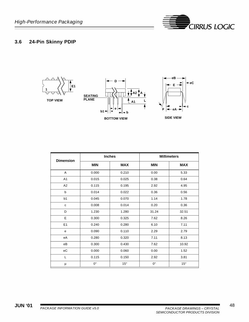
3.6 24-Pin Skinny PDIP
DimensionInches Millimeters
MIN MAX MIN MAX
A 0.000 0.210 0.00 5.33
A1 0.015 0.025 0.38 0.64
A2 0.115 0.195 2.92 4.95
b 0.014 0.022 0.36 0.56
b1 0.045 0.070 1.14 1.78
c 0.008 0.014 0.20 0.36
D 1.230 1.280 31.24 32.51
E 0.300 0.325 7.62 8.26
E1 0.240 0.280 6.10 7.11
e 0.090 0.110 2.29 2.79
eA 0.280 0.320 7.11 8.13
eB 0.300 0.430 7.62 10.92
eC 0.000 0.060 0.00 1.52
L 0.115 0.150 2.92 3.81
µ 0° 15° 0° 15°
E1
D
SEATINGPLANE
b1e
b
A
LA1
µ
TOP VIEW
BOTTOM VIEW SIDE VIEW
1
c
A2
EeC
eB
eA

PACKAGE INFORMATION GUIDE v5.0JUN ‘0149
PACKAGE DRAWINGS – CRYSTAL SEMICONDUCTOR PRODUCTS DIVISION
High-Performance Packaging
3.7 24-Pin PDIP (600-mm Body)
DimensionInches Millimeters
MIN MAX MIN MAX
A 0.000 0.250 0.00 6.35
A1 0.015 0.025 0.38 0.64
A2 0.125 0.195 3.18 4.95
b 0.014 0.022 0.36 0.56
b1 0.030 0.070 0.76 1.78
c 0.008 0.014 0.20 0.36
D 1.150 1.290 29.21 32.77
E 0.600 0.625 15.24 15.88
E1 0.485 0.580 12.32 14.73
e 0.090 0.110 2.29 2.79
eA 0.580 0.620 14.73 15.75
eB 0.600 0.700 15.24 17.78
eC 0.000 0.060 0.00 1.52
L 0.115 0.200 2.92 5.08
µ 0° 15° 0° 15°
E1
D
SEATINGPLANE
b1e
b
A
LA1
µ
TOP VIEW
BOTTOM VIEW SIDE VIEW
1
c
A2
EeC
eB
eA

JUN ‘01 50PACKAGE INFORMATION GUIDE v5.0 PACKAGE DRAWINGS – CRYSTAL
SEMICONDUCTOR PRODUCTS DIVISION
High-Performance Packaging
3.8 28-Pin PDIP (600-mm Body)
DimensionInches Millimeters
MIN MAX MIN MAX
A 0.000 0.250 0.00 6.35
A1 0.015 0.025 0.38 0.64
A2 0.125 0.195 3.18 4.95
b 0.014 0.022 0.36 0.56
b1 0.030 0.070 0.76 1.78
c 0.008 0.014 0.20 0.36
D 1.380 1.565 35.05 39.75
E 0.600 0.625 15.24 15.88
E1 0.485 0.580 12.32 14.73
e 0.090 0.110 2.29 2.79
eA 0.580 0.620 14.73 15.75
eB 0.600 0.700 15.24 17.78
eC 0.000 0.060 0.00 1.52
L 0.115 0.200 2.92 5.08
µ 0° 15° 0° 15°
E1
D
SEATINGPLANE
b1e
b
A
LA1
µ
TOP VIEW
BOTTOM VIEW SIDE VIEW
1
c
A2
EeC
eB
eA

PACKAGE INFORMATION GUIDE v5.0JUN ‘0151
PACKAGE DRAWINGS – CRYSTAL SEMICONDUCTOR PRODUCTS DIVISION
High-Performance Packaging
3.9 40-Pin PDIP (600-mm Body)
DimensionInches Millimeters
MIN MAX MIN MAX
A 0.000 0.250 0.00 6.35
A1 0.015 0.025 0.38 0.64
A2 0.125 0.195 3.18 4.95
b 0.014 0.022 0.36 0.56
b1 0.030 0.070 0.76 1.78
c 0.008 0.014 0.20 0.36
D 1.980 2.095 50.29 53.21
E 0.600 0.625 15.24 15.88
E1 0.485 0.580 12.32 14.73
e 0.090 0.110 2.29 2.79
eA 0.580 0.620 14.73 15.75
eB 0.600 0.700 15.24 17.78
eC 0.000 0.060 0.00 1.52
L 0.115 0.200 2.92 5.08
µ 0° 15° 0° 15°
E1
D
SEATINGPLANE
b1e
b
A
LA1
µ
TOP VIEW
BOTTOM VIEW SIDE VIEW
1
c
A2
EeC
eB
eA

JUN ‘01 52PACKAGE INFORMATION GUIDE v5.0 PACKAGE DRAWINGS – CRYSTAL
SEMICONDUCTOR PRODUCTS DIVISION
High-Performance Packaging
3.10 8-Pin SOIC (150-mm Body)
DimensionInches Millimeters
MIN MAX MIN MAX
A 0.053 0.069 1.35 1.75
A1 0.004 0.010 0.10 0.25
b 0.013 0.020 0.33 0.51
c 0.007 0.010 0.19 0.25
D 0.189 0.197 4.80 5.00
E 0.150 0.157 3.80 4.00
e 0.040 0.060 1.02 1.52
H 0.228 0.244 5.80 6.20
L 0.016 0.050 0.40 1.27
µ 0° 8° 0° 8°
D
HE
e
b
A1
c
L
µSEATINGPLANE
1
A

PACKAGE INFORMATION GUIDE v5.0JUN ‘0153
PACKAGE DRAWINGS – CRYSTAL SEMICONDUCTOR PRODUCTS DIVISION
High-Performance Packaging
3.11 8-Pin SOIC (209-mm Body)
DimensionInches Millimeters
MIN MAX MIN MAX
A 0.076 0.084 1.93 2.13
A1 0.004 0.010 0.10 0.25
b 0.013 0.020 0.33 0.51
c 0.006 0.010 0.15 0.25
D 0.206 0.210 5.23 5.33
E 0.204 0.212 5.18 5.38
e 0.040 0.060 1.02 1.52
H 0.302 0.318 7.67 8.08
L 0.019 0.030 0.48 0.76
µ 0° 8° 0° 8°
D
HE
e
b
A1
c
L
µSEATINGPLANE
1
A

JUN ‘01 54PACKAGE INFORMATION GUIDE v5.0 PACKAGE DRAWINGS – CRYSTAL
SEMICONDUCTOR PRODUCTS DIVISION
High-Performance Packaging
3.12 16-Pin SOIC (150-mm Body)
INCHES MILLIMETERSDIM MIN NOM MAX MIN NOM MAX
A 0.053 0.064 0.069 1.35 1.63 1.75A1 0.004 0.006 0.010 0.10 0.15 0.25b 0.013 0.016 0.020 0.33 0.41 0.51C 0.0075 0.008 0.010 0.19 0.20 0.25D 0.386 0.390 0.394 9.80 9.91 10.00E 0.150 0.154 0.157 3.80 3.90 4.00e 0.040 0.050 0.060 1.02 1.27 1.52H 0.228 0.236 0.244 5.80 6.0 6.20L 0.016 0.025 0.050 0.40 0.64 1.27∝ 0° 4° 8° 0° 4° 8°
JEDEC # : MS-012
Controling Dimension is Millimeters
e
D
HE
b
A1
A
c
L
∝SEATINGPLANE
1

PACKAGE INFORMATION GUIDE v5.0JUN ‘0155
PACKAGE DRAWINGS – CRYSTAL SEMICONDUCTOR PRODUCTS DIVISION
High-Performance Packaging
3.13 16-Pin SOIC (300-mm Body)
DimensionInches Millimeters
MIN MAX MIN MAX
A 0.093 0.104 2.35 2.65
A1 0.004 0.012 0.10 0.30
b 0.013 0.020 0.33 0.51
c 0.009 0.013 0.23 0.32
D 0.398 0.413 10.10 10.50
E 0.291 0.299 7.40 7.60
e 0.040 0.060 1.02 1.52
H 0.394 0.419 10.00 10.65
L 0.016 0.050 0.40 1.27
µ 0° 8° 0° 8°
e
D
HE
b
A1
c
L
µSEATING
PLANE
1
A

JUN ‘01 56PACKAGE INFORMATION GUIDE v5.0 PACKAGE DRAWINGS – CRYSTAL
SEMICONDUCTOR PRODUCTS DIVISION
High-Performance Packaging
3.14 20-Pin SOIC (300-mm Body)
DimensionInches Millimeters
MIN MAX MIN MAX
A 0.093 0.104 2.35 2.65
A1 0.004 0.012 0.10 0.30
b 0.013 0.020 0.33 0.51
c 0.009 0.013 0.23 0.32
D 0.496 0.512 12.60 13.00
E 0.291 0.299 7.40 7.60
e 0.040 0.060 1.02 1.52
H 0.394 0.419 10.00 10.65
L 0.016 0.050 0.40 1.27
µ 0° 8° 0° 8°
e
D
HE
b
A1
c
L
µSEATING
PLANE
1
A

PACKAGE INFORMATION GUIDE v5.0JUN ‘0157
PACKAGE DRAWINGS – CRYSTAL SEMICONDUCTOR PRODUCTS DIVISION
High-Performance Packaging
3.15 24-Pin SOIC (300-mm Body)
DimensionInches Millimeters
MIN MAX MIN MAX
A 0.093 0.104 2.35 2.65
A1 0.004 0.012 0.10 0.30
b 0.013 0.020 0.33 0.51
c 0.009 0.013 0.23 0.32
D 0.598 0.614 15.20 15.60
E 0.291 0.299 7.40 7.60
e 0.040 0.060 1.02 1.52
H 0.394 0.419 10.00 10.65
L 0.016 0.050 0.40 1.27
µ 0° 8° 0° 8°
D
HE
b
A1
c
L
µSEATING
PLANE
1
e
A

JUN ‘01 58PACKAGE INFORMATION GUIDE v5.0 PACKAGE DRAWINGS – CRYSTAL
SEMICONDUCTOR PRODUCTS DIVISION
High-Performance Packaging
3.16 28-Pin SOIC (300-mm Body)
DimensionInches Millimeters
MIN MAX MIN MAX
A 0.093 0.104 2.35 2.65
A1 0.004 0.012 0.10 0.30
b 0.013 0.020 0.33 0.51
c 0.009 0.013 0.23 0.32
D 0.697 0.713 17.70 18.10
E 0.291 0.299 7.40 7.60
e 0.040 0.060 1.02 1.52
H 0.394 0.419 10.00 10.65
L 0.016 0.050 0.40 1.27
µ 0° 8° 0° 8°
D
HE
B
A1
c
L
µSEATING
PLANE
1
e
A

PACKAGE INFORMATION GUIDE v5.0JUN ‘0159
PACKAGE DRAWINGS – CRYSTAL SEMICONDUCTOR PRODUCTS DIVISION
High-Performance Packaging
3.17 8-Pin SSOP
Notes: 1. “D” and “E1” are reference datums and do not included mold flash or protrusions, but do include mold mismatch and are measured at the parting line, mold flash or protrusions shall not exceed 0.20 mm per side.
2. Dimension “b” does not include dambar protrusion/intrusion. Allowable dambar protrusion shall be 0.13 mm total in excess of “b” dimension at maximum material condition. Dambar intrusion shall not reduce dimension “b” by more than 0.07 mm at least material condition.
3. These dimensions apply to the flat section of the lead between 0.10 and 0.25 mm from lead tips.
INCHES MILLIMETERS NOTEDIM MIN NOM MAX MIN NOM MAX
A 0.053 0.069 1.35 1.75A1 0.004 0.010 0.10 0.25A2 0.051 0.059 1.30 1.50b 0.013 0.020 0.33 0.51 2,3c 0.007 0.010 0.19 0.25D 0.189 0.197 4.80 5.00 1E 0.150 0.157 3.80 4.00e -- 0.050 -- 1.27H 0.228 0.244 5.80 6.20L 0.016 0.050 0.40 1.27L1 -- 0.042 -- 1.07∝ 0° 8° 0° 8°
8
1 4e
b2
A1
A2 A
D
SEATINGPLANE
L1
SIDE VIEW
END VIEWTOP VIEW
5
cHE
L∝
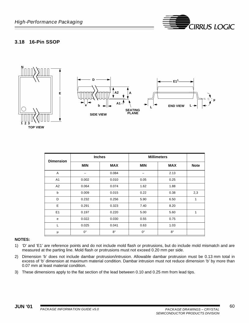
JUN ‘01 60PACKAGE INFORMATION GUIDE v5.0 PACKAGE DRAWINGS – CRYSTAL
SEMICONDUCTOR PRODUCTS DIVISION
High-Performance Packaging
3.18 16-Pin SSOP
NOTES:
1) ‘D’ and ‘E1’ are reference points and do not include mold flash or protrusions, but do include mold mismatch and aremeasured at the parting line. Mold flash or protrusions must not exceed 0.20 mm per side.
2) Dimension ‘b’ does not include dambar protrusion/intrusion. Allowable dambar protrusion must be 0.13 mm total inexcess of ‘b’ dimension at maximum material condition. Dambar intrusion must not reduce dimension ‘b’ by more than0.07 mm at least material condition.
3) These dimensions apply to the flat section of the lead between 0.10 and 0.25 mm from lead tips.
DimensionInches Millimeters
MIN MAX MIN MAX Note
A – 0.084 – 2.13
A1 0.002 0.010 0.05 0.25
A2 0.064 0.074 1.62 1.88
b 0.009 0.015 0.22 0.38 2,3
D 0.232 0.256 5.90 6.50 1
E 0.291 0.323 7.40 8.20
E1 0.197 0.220 5.00 5.60 1
e 0.022 0.030 0.55 0.75
L 0.025 0.041 0.63 1.03
µ 0° 8° 0° 8°
E
N
1 2 3
e bA1
A2 A
D
SEATINGPLANE
E11
L
SIDE VIEW
END VIEW
TOP VIEW
L
µ

PACKAGE INFORMATION GUIDE v5.0JUN ‘0161
PACKAGE DRAWINGS – CRYSTAL SEMICONDUCTOR PRODUCTS DIVISION
High-Performance Packaging
3.19 20-Pin SSOP
NOTES:
1) ‘D’ and ‘E1’ are reference points and do not include mold flash or protrusions, but do include mold mismatch and aremeasured at the parting line. Mold flash or protrusions must not exceed 0.20 mm per side.
2) Dimension ‘b’ does not include dambar protrusion/intrusion. Allowable dambar protrusion must be 0.13 mm total inexcess of ‘b’ dimension at maximum material condition. Dambar intrusion must not reduce dimension ‘b’ by more than0.07 mm at least material condition.
3) These dimensions apply to the flat section of the lead between 0.10 and 0.25 mm from lead tips.
DimensionInches Millimeters
MIN MAX MIN MAX Note
A – 0.084 – 2.13
A1 0.002 0.010 0.05 0.25
A2 0.064 0.074 1.62 1.88
b 0.009 0.015 0.22 0.38 2,3
D 0.272 0.295 6.90 7.50 1
E 0.291 0.323 7.40 8.20
E1 0.197 0.220 5.00 5.60 1
e 0.022 0.030 0.55 0.75
L 0.025 0.041 0.63 1.03
µ 0° 8° 0° 8°
E
N
1 2 3
eA1
A2 A
D
SEATINGPLANE
E11
L
SIDE VIEW
END VIEW
TOP VIEW
b2 L
µ

JUN ‘01 62PACKAGE INFORMATION GUIDE v5.0 PACKAGE DRAWINGS – CRYSTAL
SEMICONDUCTOR PRODUCTS DIVISION
High-Performance Packaging
3.20 24-Pin SSOP
NOTES:
1) ‘D’ and ‘E1’ are reference points and do not include mold flash or protrusions, but do include mold mismatch and aremeasured at the parting line. Mold flash or protrusions must not exceed 0.20 mm per side.
2) Dimension ‘b’ does not include dambar protrusion/intrusion. Allowable dambar protrusion must be 0.13 mm total inexcess of ‘b’ dimension at maximum material condition. Dambar intrusion must not reduce dimension ‘b’ by more than0.07 mm at least material condition.
3) These dimensions apply to the flat section of the lead between 0.10 and 0.25 mm from lead tips.
DimensionInches Millimeters
NoteMIN MAX MIN MAX
A – 0.084 – 2.13
A1 0.002 0.010 0.05 0.25
A2 0.064 0.074 1.62 1.88
b 0.009 0.015 0.22 0.38 2,3
D 0.311 0.335 7.90 8.50 1
E 0.291 0.323 7.40 8.20
E1 0.197 0.220 5.00 5.60 1
e 0.022 0.030 0.55 0.75
L 0.025 0.041 0.63 1.03
µ 0° 8° 0° 8°
E
N
1 2 3
e b2A1
A2 A
D
SEATINGPLANE
E11
L
SIDE VIEW
END VIEW
TOP VIEW
L
µ

PACKAGE INFORMATION GUIDE v5.0JUN ‘0163
PACKAGE DRAWINGS – CRYSTAL SEMICONDUCTOR PRODUCTS DIVISION
High-Performance Packaging
3.21 28-Pin SSOP
NOTES:
1) ‘D’ and ‘E1’ are reference points and do not include mold flash or protrusions, but do include mold mismatch and aremeasured at the parting line. Mold flash or protrusions must not exceed 0.20 mm per side.
2) Dimension ‘b’ does not include dambar protrusion/intrusion. Allowable dambar protrusion must be 0.13 mm total inexcess of ‘b’ dimension at maximum material condition. Dambar intrusion must not reduce dimension ‘b’ by more than0.07 mm at least material condition.
3) These dimensions apply to the flat section of the lead between 0.10 and 0.25 mm from lead tips.
DimensionInches Millimeters
NoteMIN MAX MIN MAX
A – 0.084 – 2.13
A1 0.002 0.010 0.05 0.25
A2 0.064 0.074 1.62 1.88
b 0.009 0.015 0.22 0.38 2,3
D 0.390 0.413 9.90 10.50 1
E 0.291 0.323 7.40 8.20
E1 0.197 0.220 5.00 5.60 1
e 0.022 0.030 0.55 0.75
L 0.025 0.041 0.63 1.03
µ 0° 8° 0° 8°
E
N
1 2 3
e b2A1
A2 A
D
SEATINGPLANE
E11
L
SIDE VIEW
END VIEW
TOP VIEW
L
µ

JUN ‘01 64PACKAGE INFORMATION GUIDE v5.0 PACKAGE DRAWINGS – CRYSTAL
SEMICONDUCTOR PRODUCTS DIVISION
High-Performance Packaging
3.22 16L TSSOP (4.4-mm Body)
Notes: 1. “D” and “E1” are reference datums and do not included mold flash or protrusions, but do include mold mismatch and are measured at the parting line, mold flash or protrusions shall not exceed 0.20 mm per side.
2. Dimension “b” does not include dambar protrusion/intrusion. Allowable dambar protrusion shall be 0.13 mm total in excess of “b” dimension at maximum material condition. Dambar intrusion shall not reduce dimension “b” by more than 0.07 mm at least material condition.
3. These dimensions apply to the flat section of the lead between 0.10 and 0.25 mm from lead tips.
INCHES MILLIMETERS NOTEDIM MIN NOM MAX MIN NOM MAX
A -- -- 0.043 -- -- 1.10A1 0.002 0.004 0.006 0.05 -- 0.15A2 0.03346 0.0354 0.037 0.85 0.90 0.95b 0.00748 0.0096 0.012 0.19 0.245 0.30 2,3D 0.193 0.1969 0.201 4.90 5.00 5.10 1E 0.248 0.2519 0.256 6.30 6.40 6.50
E1 0.169 0.1732 0.177 4.30 4.40 4.50 1e -- 0.026 BSC -- -- 0.065 BSC --L 0.020 0.024 0.028 0.50 0.60 0.70∝ 0° 4° 8° 0° 4° 8°
JEDEC #: MO-153
Controlling Dimension is Millimeters
E
N
1 2 3
e b2 A1
A2 A
D
SEATINGPLANE
E11
L
SIDE VIEW
END VIEW
TOP VIEW
∝
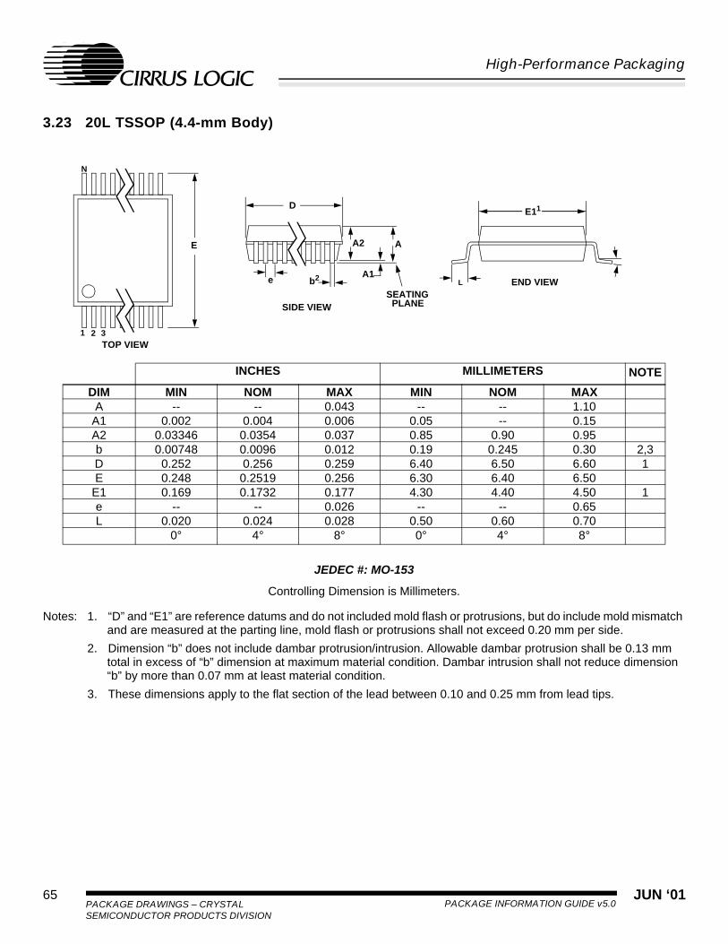
PACKAGE INFORMATION GUIDE v5.0JUN ‘0165
PACKAGE DRAWINGS – CRYSTAL SEMICONDUCTOR PRODUCTS DIVISION
High-Performance Packaging
3.23 20L TSSOP (4.4-mm Body)
Notes: 1. “D” and “E1” are reference datums and do not included mold flash or protrusions, but do include mold mismatch and are measured at the parting line, mold flash or protrusions shall not exceed 0.20 mm per side.
2. Dimension “b” does not include dambar protrusion/intrusion. Allowable dambar protrusion shall be 0.13 mm total in excess of “b” dimension at maximum material condition. Dambar intrusion shall not reduce dimension “b” by more than 0.07 mm at least material condition.
3. These dimensions apply to the flat section of the lead between 0.10 and 0.25 mm from lead tips.
INCHES MILLIMETERS NOTE
DIM MIN NOM MAX MIN NOM MAXA -- -- 0.043 -- -- 1.10
A1 0.002 0.004 0.006 0.05 -- 0.15A2 0.03346 0.0354 0.037 0.85 0.90 0.95b 0.00748 0.0096 0.012 0.19 0.245 0.30 2,3D 0.252 0.256 0.259 6.40 6.50 6.60 1E 0.248 0.2519 0.256 6.30 6.40 6.50
E1 0.169 0.1732 0.177 4.30 4.40 4.50 1e -- -- 0.026 -- -- 0.65L 0.020 0.024 0.028 0.50 0.60 0.70∝ 0° 4° 8° 0° 4° 8°
JEDEC #: MO-153
Controlling Dimension is Millimeters.
E
N
1 2 3
e b2 A1
A2 A
D
SEATINGPLANE
E11
L
SIDE VIEW
END VIEW
TOP VIEW
∝

JUN ‘01 66PACKAGE INFORMATION GUIDE v5.0 PACKAGE DRAWINGS – CRYSTAL
SEMICONDUCTOR PRODUCTS DIVISION
High-Performance Packaging
3.24 24L TSSOP (4.4-mm Body)
Notes: 1. “D” and “E1” are reference datums and do not included mold flash or protrusions, but do include mold mismatch and are measured at the parting line, mold flash or protrusions shall not exceed 0.20 mm per side.
2. Dimension “b” does not include dambar protrusion/intrusion. Allowable dambar protrusion shall be 0.13 mm total in excess of “b” dimension at maximum material condition. Dambar intrusion shall not reduce dimension “b” by more than 0.07 mm at least material condition.
3. These dimensions apply to the flat section of the lead between 0.10 and 0.25 mm from lead tips.
INCHES MILLIMETERS NOTE
DIM MIN NOM MAX MIN NOM MAXA -- -- 0.043 -- -- 1.10A1 0.002 0.004 0.006 0.05 -- 0.15A2 0.03346 0.0354 0.037 0.85 0.90 0.95b 0.00748 0.0096 0.012 0.19 0.245 0.30 2,3D 0.303 0.307 0.311 7.70 7.80 7.90 1E 0.248 0.2519 0.256 6.30 6.40 6.50E1 0.169 0.1732 0.177 4.30 4.40 4.50 1e -- 0.026 BSC -- -- 0.65 BSC --L 0.020 0.024 0.028 0.50 0.60 0.70∝ 0° 4° 8° 0° 4° 8°
JEDEC #: MO-153Controlling Dimension is Millimeters.
E
N
1 2 3
e b2 A1
A2 A
D
SEATINGPLANE
E11
L
SIDE VIEW
END VIEW
TOP VIEW
∝

PACKAGE INFORMATION GUIDE v5.0JUN ‘0167
PACKAGE DRAWINGS – CRYSTAL SEMICONDUCTOR PRODUCTS DIVISION
High-Performance Packaging
3.25 48-Pin TSSOP (6.1-mm Body)
NOTES:
1) ‘D’ and ‘E1’ are reference points and do not include mold flash or protrusions, but do include mold mismatch and aremeasured at the parting line. Mold flash or protrusions must not exceed 0.20 mm per side.
2) Dimension ‘b’ does not include dambar protrusion/intrusion. Allowable dambar protrusion must be 0.13 mm total inexcess of ‘b’ dimension at maximum material condition. Dambar intrusion must not reduce dimension ‘b’ by more than0.07 mm at least material condition.
3) These dimensions apply to the flat section of the lead between 0.10 and 0.25 mm from lead tips.
DimensionInches Millimeters
NoteMIN MAX MIN MAX
A – 0.047 – 1.20
A1 0.002 0.006 0.05 0.15
A2 0.031 0.041 0.80 1.05
b 0.007 0.011 0.17 0.27 2,3
D 0.488 0.496 12.40 12.60 1
E 0.313 0.325 7.95 8.25
E1 0.236 0.244 6.00 6.20 1
e 0.016 0.024 0.40 0.60
L 0.018 0.030 0.45 0.75
µ 0° 8° 0° 8°
E
N
1 2 3
e b2A1
A2 A
D
SEATINGPLANE
E11
L
SIDE VIEW
END VIEW
TOP VIEW
L
µ

JUN ‘01 68PACKAGE INFORMATION GUIDE v5.0 PACKAGE DRAWINGS – CRYSTAL
SEMICONDUCTOR PRODUCTS DIVISION
High-Performance Packaging
3.26 44-Pin TQFP
DimensionInches Millimeters
MIN MAX MIN MAX
A 0.000 0.065 0.00 1.60
A1 0.002 0.006 0.05 0.15
B 0.012 0.018 0.30 0.45
D 0.478 0.502 11.70 12.30
D1 0.404 0.412 9.90 10.10
E 0.478 0.502 11.70 12.30
E1 0.404 0.412 9.90 10.10
e 0.029 0.037 0.70 0.90
L 0.018 0.030 0.45 0.75
µ 0° 7° 0° 7°
E1
E
D1D
1
e
L
µ
B
A1
A

PACKAGE INFORMATION GUIDE v5.0JUN ‘0169
PACKAGE DRAWINGS – CRYSTAL SEMICONDUCTOR PRODUCTS DIVISION
High-Performance Packaging
3.27 48-Pin TQFP
DimensionInches Millimeters
MIN MAX MIN MAX
A 0.000 0.063 0.00 1.60
A1 0.002 0.006 0.05 0.15
B 0.007 0.011 0.17 0.27
D 0.343 0.366 8.70 9.30
D1 0.272 0.280 6.90 7.10
E 0.343 0.366 8.70 9.30
E1 0.272 0.280 6.90 7.10
e 0.016 0.024 0.40 0.60
L 0.018 0.030 0.45 0.75
µ 0° 7° 0° 7°
E1
E
D1D
1
e
L
µ
B
A1
A

JUN ‘01 70PACKAGE INFORMATION GUIDE v5.0 PACKAGE DRAWINGS – CRYSTAL
SEMICONDUCTOR PRODUCTS DIVISION
High-Performance Packaging
3.28 64-Pin TQFP
DimensionInches Millimeters
MIN MAX MIN MAX
A 0.000 0.063 0.00 1.60
A1 0.002 0.006 0.05 0.15
B 0.007 0.011 0.17 0.27
D 0.461 0.484 11.70 12.30
D1 0.390 0.398 9.90 10.10
E 0.461 0.484 11.70 12.30
E1 0.390 0.398 9.90 10.10
e 0.016 0.024 0.40 0.60
L 0.018 0.030 0.45 0.75
µ 0° 7° 0° 7°
E1
E
D1D
1
e
L
µ
B
A1
A

PACKAGE INFORMATION GUIDE v5.0JUN ‘0171
PACKAGE DRAWINGS – CRYSTAL SEMICONDUCTOR PRODUCTS DIVISION
High-Performance Packaging
3.29 100-Pin TQFP
DimensionInches Millimeters
MIN MAX MIN MAX
A 0.000 0.063 0.00 1.60
A1 0.002 0.006 0.05 0.15
B 0.007 0.011 0.17 0.27
D 0.618 0.642 15.70 16.30
D1 0.547 0.555 13.90 14.10
E 0.618 0.642 15.70 16.30
E1 0.547 0.555 13.90 14.10
e 0.016 0.024 0.40 0.60
L 0.018 0.030 0.45 0.75
µ 0° 7° 0° 7°
E1
E
D1D
1
e
L
µ
B
A1
A

JUN ‘01 72PACKAGE INFORMATION GUIDE v5.0 PACKAGE DRAWINGS – CRYSTAL
SEMICONDUCTOR PRODUCTS DIVISION
High-Performance Packaging
3.30 100-Pin MQFP
DimensionInches Millimeters
MIN MAX MIN MAX
A 0.000 0.134 0.000 3.400
A1 0.010 0.014 0.250 0.350
B 0.009 0.015 0.220 0.380
D 0.667 0.687 16.950 17.450
D1 0.547 0.555 13.900 14.100
E 0.904 0.923 22.950 23.450
E1 0.783 0.791 19.900 20.100
e 0.022 0.030 0.550 0.750
µ 0° 7° 0° 7°
L 0.018 0.030 0.450 0.750
E1
E
D1D
1
e
L
µ
B
A1
A

PACKAGE INFORMATION GUIDE v5.0JUN ‘0173
PACKAGE DRAWINGS – CRYSTAL SEMICONDUCTOR PRODUCTS DIVISION
High-Performance Packaging
3.31 128-Pin TQFP
DimensionInches Millimeters
MIN MAX MIN MAX
A 0.000 0.063 0.000 1.600
A1 0.002 0.006 0.050 0.150
B 0.007 0.011 0.170 0.270
D 0.626 0.634 15.900 16.100
D1 0.547 0.555 13.900 14.100
E 0.862 0.870 21.900 22.100
E1 0.783 0.791 19.900 20.100
e 0.016 0.024 0.400 0.600
µ 0° 7° 0° 7°
L 0.018 0.030 0.450 0.750
E1
E
D1D
1
e
L
µ
B
A1
A

JUN ‘01 74PACKAGE INFORMATION GUIDE v5.0 PACKAGE DRAWINGS – CRYSTAL
SEMICONDUCTOR PRODUCTS DIVISION
High-Performance Packaging
3.32 144-Pin TQFP
DimensionInches Millimeters
MIN MAX MIN MAX
A 0.000 0.063 0.00 1.60
A1 0.002 0.006 0.05 0.15
B 0.007 0.011 0.17 0.27
D 0.854 0.878 21.70 22.30
D1 0.783 0.791 19.90 20.10
E 0.854 0.878 21.70 22.30
E1 0.783 0.791 19.90 20.10
e 0.016 0.024 0.40 0.60
L 0.018 0.030 0.45 0.75
µ 0° 7° 0° 7°
E1E
D1D
1
e
L
µ
B
A1
A

PACKAGE INFORMATION GUIDE v5.0JUN ‘0175
PACKAGE DRAWINGS – CRYSTAL SEMICONDUCTOR PRODUCTS DIVISION
High-Performance Packaging
3.33 28-Pin PLCC
DimensionInches Millimeters
MIN MAX MIN MAX
A 0.165 0.180 4.043 4.572
A1 0.090 0.120 2.205 3.048
B 0.013 0.021 0.319 0.533
D 0.485 0.495 11.883 12.573
D1 0.450 0.456 11.025 11.582
D2 0.390 0.430 9.555 10.922
E 0.485 0.495 11.883 12.573
E1 0.450 0.456 11.025 11.582
E2 0.390 0.430 9.555 10.922
e 0.040 0.060 0.980 1.524
D1
D
E1 E D2/E2
B
e
A1
A

JUN ‘01 76PACKAGE INFORMATION GUIDE v5.0 PACKAGE DRAWINGS – CRYSTAL
SEMICONDUCTOR PRODUCTS DIVISION
High-Performance Packaging
3.34 44-Pin PLCC
DimensionInches Millimeters
MIN MAX MIN MAX
A 0.165 0.180 4.043 4.572
A1 0.090 0.120 2.205 3.048
B 0.013 0.021 0.319 0.533
D 0.685 0.695 16.783 17.653
D1 0.650 0.656 15.925 16.662
D2 0.590 0.630 14.455 16.002
E 0.685 0.695 16.783 17.653
E1 0.650 0.656 15.925 16.662
E2 0.590 0.630 14.455 16.002
e 0.040 0.060 0.980 1.524
D1
D
E1 E D2/E2
B
e
A1
A

PACKAGE INFORMATION GUIDE v5.0JUN ‘0177
PACKAGE DRAWINGS – CRYSTAL SEMICONDUCTOR PRODUCTS DIVISION
High-Performance Packaging
3.35 68-Pin PLCC
DimensionInches Millimeters
MIN MAX MIN MAX
A 0.165 0.180 4.043 4.572
A1 0.090 0.120 2.205 3.048
B 0.013 0.021 0.319 0.533
D 0.985 0.995 24.133 25.273
D1 0.950 0.958 23.275 24.333
D2 0.890 0.930 21.805 23.622
E 0.985 0.995 24.133 25.273
E1 0.950 0.958 23.275 24.333
E2 0.890 0.930 21.805 23.622
e 0.040 0.060 0.980 1.524
D1
D
E1 E D2/E2
B
e
A1
A

JUN ‘01 78PACKAGE INFORMATION GUIDE v5.0 TRAY DRAWINGS
High-Performance Packaging
4. TRAY DRAWINGS
4.1 10 × 10 × 1.4-mm Body LQFP Tray
B1
(2x)
T1
T2T3 (4x)
A3
A2
B3
B2
B4
CH
AM
A6 A7
B5
A4
R1
R2
R3
R4
(19x)
(7x)
CHAM
B6
(2x)
Scale: 3x
AA1
B
A5 (2x)(2x) (4x)
NOTES:
1) Center closed nests are for vacuum operations.
2) Interpret dimensions and tolerances in accordance withANSI Y14.5M-1982.
3) Unless otherwise noted, 1°/2° draft on all vertical sur-faces.
4) Locking notches. 4 places.
5) Trays should not be exposed to temperatures greaterthan 125°C for 24 hours.
Figure Reference TYP (mm) Figure Reference TYP (mm)
A 322.60 B3 13.00
A1 315.00 B4 2.0 × 45°
A2 13.10 B5 0.76
A3 15.20 B6 12.7
A4 3.0 × 45° T1 7.62
A5 255.3 T2 1.27 ±0.13
A6 34.3 T3 2.54
A7 25.4 R1 2.54
B 135.90 R2 4.75
B1 92.10 R3 1.00
B2 15.70 R4 1.60
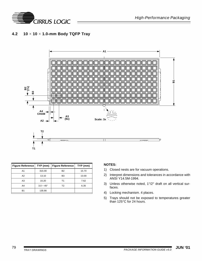
PACKAGE INFORMATION GUIDE v5.0JUN ‘0179
TRAY DRAWINGS
High-Performance Packaging
4.2 10 × 10 × 1.0-mm Body TQFP Tray
T1
T2
A3
A2
B3
B2
(7x)
Scale: 3x
A4CHAM
A1
(9x)
B1
NOTES:
1) Closed nests are for vacuum operations.
2) Interpret dimensions and tolerances in accordance withANSI Y14.5M-1994.
3) Unless otherwise noted, 1°/2° draft on all vertical sur-faces.
4) Locking mechanism. 4 places.
5) Trays should not be exposed to temperatures greaterthan 125°C for 24 hours.
Figure Reference TYP (mm) Figure Reference TYP (mm)
A1 315.00 B2 15.70
A2 13.10 B3 13.00
A3 15.20 T1 7.62
A4 3.0 × 45° T2 6.35
B1 135.90
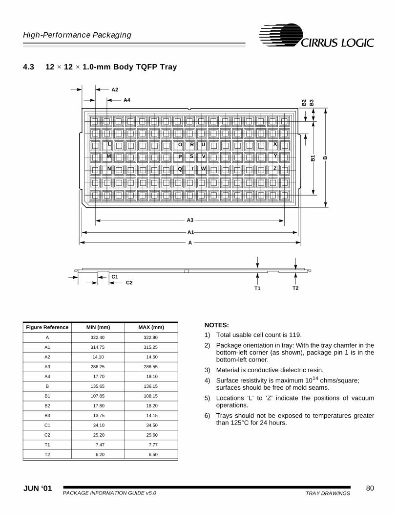
JUN ‘01 80PACKAGE INFORMATION GUIDE v5.0 TRAY DRAWINGS
High-Performance Packaging
4.3 12 × 12 × 1.0-mm Body TQFP Tray
A4
A2
B2
T1 T2
L
M
C1C2
N
O
P
Q
R
S
T
U
V
W
X
Y
Z
B3
B1 B
A
A1
A3
NOTES:
1) Total usable cell count is 119.
2) Package orientation in tray: With the tray chamfer in thebottom-left corner (as shown), package pin 1 is in thebottom-left corner.
3) Material is conductive dielectric resin.
4) Surface resistivity is maximum 1014 ohms/square; surfaces should be free of mold seams.
5) Locations ‘L’ to ‘Z’ indicate the positions of vacuumoperations.
6) Trays should not be exposed to temperatures greaterthan 125°C for 24 hours.
Figure Reference MIN (mm) MAX (mm)
A 322.40 322.80
A1 314.75 315.25
A2 14.10 14.50
A3 286.25 286.55
A4 17.70 18.10
B 135.65 136.15
B1 107.85 108.15
B2 17.80 18.20
B3 13.75 14.15
C1 34.10 34.50
C2 25.20 25.60
T1 7.47 7.77
T2 6.20 6.50
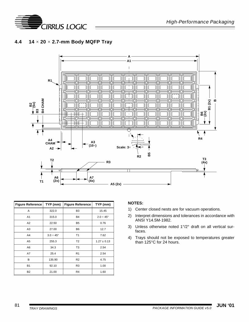
PACKAGE INFORMATION GUIDE v5.0JUN ‘0181
TRAY DRAWINGS
High-Performance Packaging
4.4 14 × 20 × 2.7-mm Body MQFP Tray
T1
T2 T3
A3
A2
B3
B2
B4
CH
AM
A6 A7
B5
A4
R1
R2
R3
R4
(10×)
(5x)
CHAM
B6
(2x)
Scale: 3×
AA1
A5 (2x)(4x)(2x)
(4x)
B1
(2x) B
NOTES:
1) Center closed nests are for vacuum operations.
2) Interpret dimensions and tolerances in accordance withANSI Y14.5M-1982.
3) Unless otherwise noted 1°/2° draft on all vertical sur-faces.
4) Trays should not be exposed to temperatures greaterthan 125°C for 24 hours.
Figure Reference TYP (mm) Figure Reference TYP (mm)
A 322.0 B3 15.45
A1 315.0 B4 2.0 × 45°
A2 22.50 B5 0.76
A3 27.00 B6 12.7
A4 3.0 × 45° T1 7.62
A5 255.3 T2 1.27 ± 0.13
A6 34.3 T3 2.54
A7 25.4 R1 2.54
B 135.90 R2 4.75
B1 92.10 R3 1.00
B2 21.00 R4 1.60
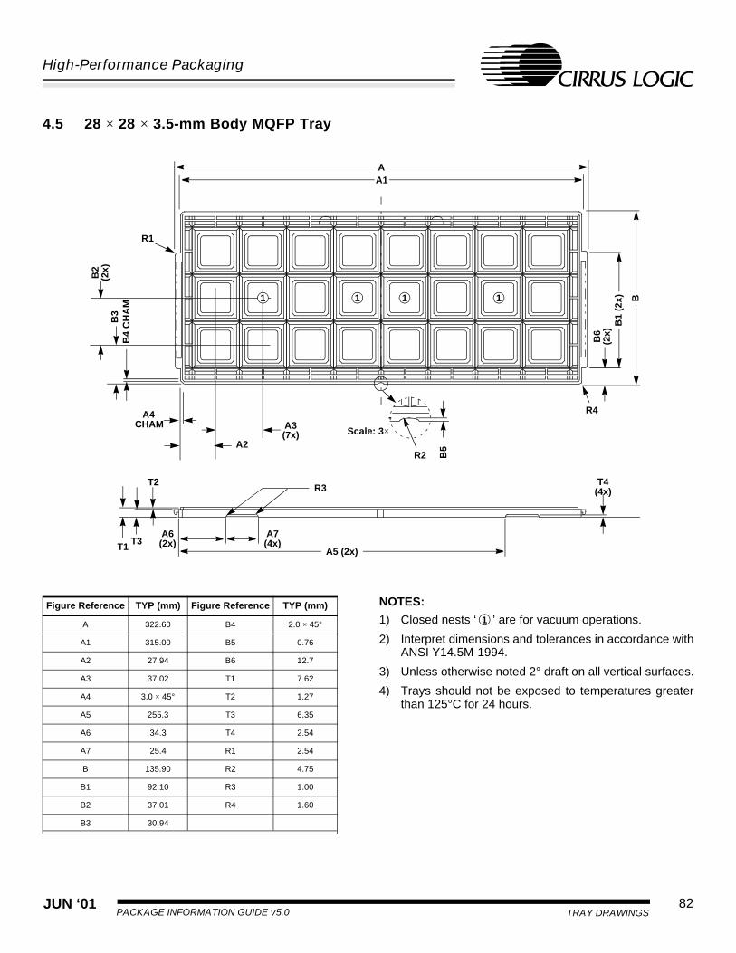
JUN ‘01 82PACKAGE INFORMATION GUIDE v5.0 TRAY DRAWINGS
High-Performance Packaging
4.5 28 × 28 × 3.5-mm Body MQFP Tray
T1
T2 T4
A3
A2
B3
B2
B4
CH
AM
A6 A7
B5
A4
R1
R2
R3
R4
(7x)
(2x)
CHAM
B6
(2x)
Scale: 3×
T3
AA1
(4x)(2x)A5 (2x)
(4x)
B1
(2x) B1 1 11
NOTES:
1) Closed nests ‘ ’ are for vacuum operations.
2) Interpret dimensions and tolerances in accordance withANSI Y14.5M-1994.
3) Unless otherwise noted 2° draft on all vertical surfaces.
4) Trays should not be exposed to temperatures greaterthan 125°C for 24 hours.
Figure Reference TYP (mm) Figure Reference TYP (mm)
A 322.60 B4 2.0 × 45°
A1 315.00 B5 0.76
A2 27.94 B6 12.7
A3 37.02 T1 7.62
A4 3.0 × 45° T2 1.27
A5 255.3 T3 6.35
A6 34.3 T4 2.54
A7 25.4 R1 2.54
B 135.90 R2 4.75
B1 92.10 R3 1.00
B2 37.01 R4 1.60
B3 30.94
1

PACKAGE INFORMATION GUIDE v5.0JUN ‘0183
TRAY DRAWINGS
High-Performance Packaging
4.6 32 × 32 × 3.5-mm Body MQFP Tray
T1
T2 T3
A3A2
B3
B2
B4
CH
AM
A6 A7
B5
A4
R1
R2
R3
R4
(7x)
(2x)
CHAM
B6
(2x)
Scale: 3x
AA1
B1
(2x) B
(2x) (4x)A5 (2x)
(4x)
1 1 1 1
NOTES:
1) Closed nests ‘ ’ are for vacuum operations: 4 places.
2) Interpret dimensions and tolerances in accordance withANSI Y14.5M-1982.
3) Unless otherwise noted 1°/2° draft on all vertical sur-faces.
4) Width-wise rib at these locations is 4.00 mm high.
5) Trays should not be exposed to temperatures greaterthan 125°C for 24 hours.
Figure Reference TYP (mm) Figure Reference TYP (mm)
A 322.60 B3 26.57
A1 315.00 B4 2.0 × 45°
A2 25.13 B5 0.76
A3 37.82 B6 12.7 ±0.13
A4 3.0 × 45° T1 7.62
A5 255.3 T2 1.27
A6 34.3 T3 2.54
A7 25.4 R1 2.54
B 135.90 R2 4.75
B1 92.10 R3 1.00
B2 41.38 R4 1.60
1

JUN ‘01 84PACKAGE INFORMATION GUIDE v5.0 TRAY DRAWINGS
High-Performance Packaging
4.7 14 × 14 × 1.4-mm Body LQFP Tray
R4
B6
(2x)
R1
A3
A2
B3
B2
B4
CH
AM
A4
(14x)
(5x)
CHAM
B5
R2
Scale: 3x
T1
T3 T4
A6 A7
R3
(4x)
(3x)
T2
A
A1
B1
(2x) B
(2x) (4x)A5 (2x)
(4x)
NOTES:
1) Center closed nests are for vacuum operations.
2) Interpret dimensions and tolerances in accordance withANSI Y14.5M-1982.
3) Unless otherwise noted 1°/2° draft on all vertical sur-faces.
4) Trays should not be exposed to temperatures greaterthan 125°C for 24 hours.
Figure Reference TYP. (mm) Figure Reference TYP. (mm)
A 322.60 B4 2.0 × 45°
A1 315.00 B5 0.76
A2 15.40 B6 12.7
A3 20.20 T1 7.62
A4 3.0 × 45° T2 6.35
A5 255.3 T3 1.27
A6 34.3 T4 2.54
A7 25.4 R1 2.54
B 135.90 R2 4.75
B1 92.10 R3 1.00
B2 21.00 R4 1.60
B3 15.45

PACKAGE INFORMATION GUIDE v5.0JUN ‘0185
TRAY DRAWINGS
High-Performance Packaging
4.8 14 × 20 × 1.4-mm Body LQFP Tray
T1 T2
T3
A3A2
B3
B2
A4 R1
(11x)
(5x)
CHAMScale: 3x
A1
B1
(3x)
1
1
1
1
1
1
NOTES:
1) Closed nests ‘ ’ are for vacuum operations: 4 places.
2) Interpret dimensions and tolerances in accordance withANSI Y14.5M-1994.
3) Unless otherwise noted 1°/2° draft on all vertical sur-faces.
4) Locking mechanism; 4 places.
5) Trays should not be exposed to temperatures greaterthan 125°C for 24 hours.
Figure Reference TYP (mm) Figure Reference TYP (mm)
A1 315.00 B3 15.45
A2 17.80 T1 7.62
A3 25.40 T2 6.35
A4 3.00 × 45° T3 1.27
B1 135.90 R1 1.60
B2 21.00
1
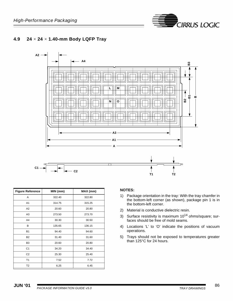
JUN ‘01 86PACKAGE INFORMATION GUIDE v5.0 TRAY DRAWINGS
High-Performance Packaging
4.9 24 × 24 × 1.40-mm Body LQFP Tray
A4
A2
B2
T1 T2
L
N
M
O
C1C2
B3
A3
A1
A
BB1
NOTES:
1) Package orientation in the tray: With the tray chamfer inthe bottom-left corner (as shown), package pin 1 is inthe bottom-left corner.
2) Material is conductive dielectric resin.
3) Surface resistivity is maximum 1014 ohms/square; sur-faces should be free of mold seams.
4) Locations ‘L’ to ‘O’ indicate the positions of vacuumoperations.
5) Trays should not be exposed to temperatures greaterthan 125°C for 24 hours.
Figure Reference MIN (mm) MAX (mm)
A 322.40 322.80
A1 314.75 315.25
A2 20.60 20.80
A3 273.50 273.70
A4 30.30 30.50
B 135.65 136.15
B1 94.40 94.60
B2 31.40 31.60
B3 20.60 20.80
C1 34.20 34.40
C2 25.30 25.40
T1 7.52 7.72
T2 6.25 6.45

PACKAGE INFORMATION GUIDE v5.0JUN ‘0187
TRAY DRAWINGS
High-Performance Packaging
4.10 28 × 28 × 1.40-mm Body LQFP Tray
A2
B2
T1 T2
L
N
M
O
CC1
B3
P
Q
B1 B
A3
A1
A
NOTES:
1) Surfaces should be free of mold seams.
2) Package orientation in tray: With the tray chamfer in thebottom-left corner (as shown), package pin 1 is in thebottom-left corner.
3) Material is conductive dielectric resin.
4) Surface resistivity is maximum 1014 ohms/square.
5) Locations ‘L’ to ‘Q’ indicate the positions (at the mini-mum) of vacuum operations.
6) Trays should not be exposed to temperatures greaterthan 125°C for 24 hours.
Figure Reference MIN (mm) MAX (mm)
A 322.35 322.85
A1 314.75 315.25
A2 28.57 28.83
A3 257.35 257.85
B 135.65 136.15
B1 96.35 96.85
B2 32.07 32.33
B3 19.52 19.78
T1 7.49 7.75
T2 6.09 6.35
C 34.05 34.55
C1 25.15 25.65

JUN ‘01 88PACKAGE INFORMATION GUIDE v5.0 TRAY DRAWINGS
High-Performance Packaging
4.11 28 × 28 × 2.00-mm Body LQFP Tray
A4
A2
B2
T1 T2
L
N
M
O
C1
C2
B3
B1 B
A
A3
A1
NOTES:
1) Surfaces should be free of mold seams.
2) Package orientation in the tray: With the tray chamfer inthe bottom-left corner (as shown), package pin 1 is inthe bottom-left corner.
3) Material is conductive dielectric resin.
4) Surface resistivity is maximum 1014 ohms/square.
5) Locations ‘L’ to ‘O’ indicate the positions of vacuumoperations.
6) Trays should not be exposed to temperatures greaterthan 125°C for 24 hours.
Figure Reference MIN (mm) MAX (mm)
A 322.40 322.80
A1 314.75 315.25
A2 32.30 32.70
A3 257.40 257.80
A4 32.00 32.40
B 135.65 136.15
B1 96.40 96.80
B2 32.10 32.30
B3 19.55 19.75
C1 34.20 34.40
C2 25.30 25.50
T1 7.67 7.97
T2 6.20 6.50

PACKAGE INFORMATION GUIDE v5.0JUN ‘0189
TRAY DRAWINGS
High-Performance Packaging
4.12 27 × 27 × 1.60-mm Body BGA Tray
T1 T2
A3
A2
B3
B2
(3x)
Scale: 3x
(9x)
A1
B1
NOTES:
1) Center closed nests are for vacuum operations.
2) Interpret dimensions and tolerances in accordance withANSI Y14.5M-1994.
3) Unless otherwise noted 1°/2° draft on all vertical sur-faces.
4) Trays should not be exposed to temperatures greaterthan 125°C for 24 hours.
Figure Reference TYP (mm) Figure Reference TYP (mm)
A1 315.00 B2 29.20
A2 26.10 B3 24.15
A3 29.20 T1 7.62
B1 135.90 T2 6.35
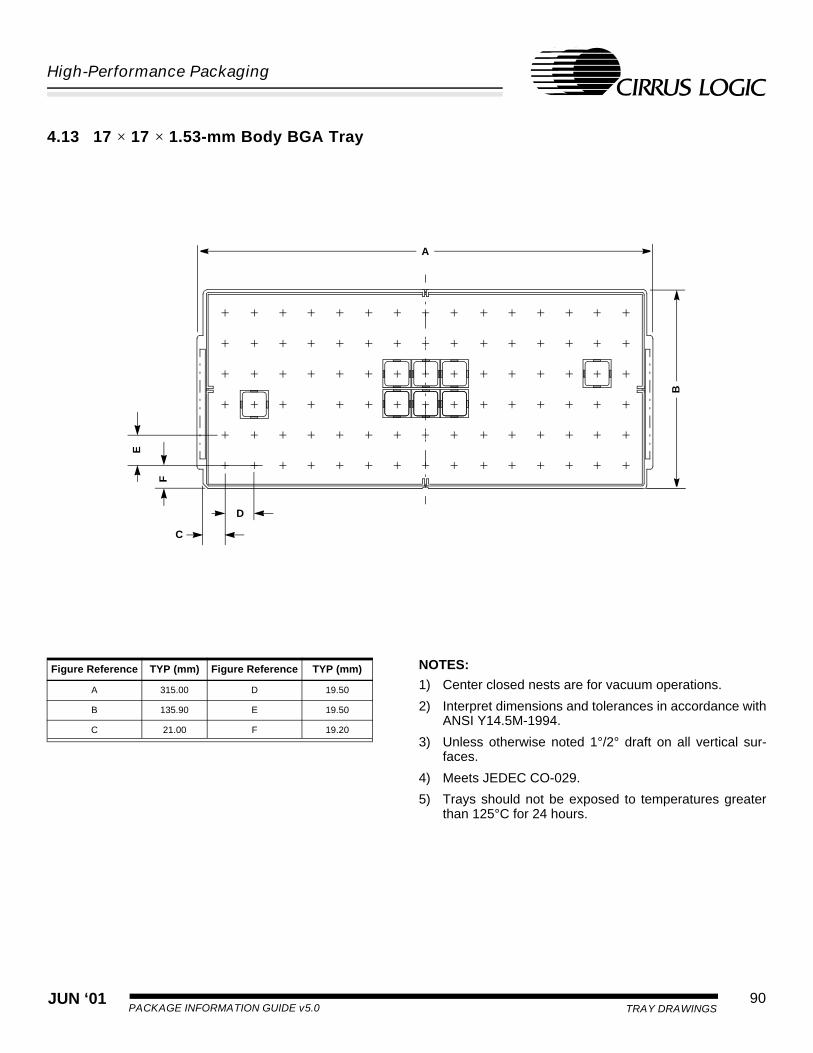
JUN ‘01 90PACKAGE INFORMATION GUIDE v5.0 TRAY DRAWINGS
High-Performance Packaging
4.13 17 × 17 × 1.53-mm Body BGA Tray
D
C
F
E
A
BNOTES:
1) Center closed nests are for vacuum operations.
2) Interpret dimensions and tolerances in accordance withANSI Y14.5M-1994.
3) Unless otherwise noted 1°/2° draft on all vertical sur-faces.
4) Meets JEDEC CO-029.
5) Trays should not be exposed to temperatures greaterthan 125°C for 24 hours.
Figure Reference TYP (mm) Figure Reference TYP (mm)
A 315.00 D 19.50
B 135.90 E 19.50
C 21.00 F 19.20

PACKAGE INFORMATION GUIDE v5.0JUN ‘0191
TRAY DRAWINGS
High-Performance Packaging
4.14 12 × 12 × 1.20-mm Body BGA Tray
D
C
F
E
A
BNOTES:
1) Center closed nests are for vacuum operations.
2) Interpret dimensions and tolerances in accordance withANSI Y14.5M-1994.
3) Unless otherwise noted 1°/2° draft on all vertical sur-faces.
4) Meets JEDEC CO-029.
5) Trays should not be exposed to temperatures greaterthan 125°C for 24 hours.
Figure Reference TYP (mm) Figure Reference TYP (mm)
A 315.00 D 14.00
B 135.90 E 11.95
C 10.50 F 14.00

JUN ‘01 92PACKAGE INFORMATION GUIDE v5.0 TECHNOLOGY ROADMAP
High-Performance Packaging
5. TECHNOLOGY ROADMAP
Please contact the Packaging and Assembly Technologies Department for updates to new packages and theirrelease dates.
6. QFP HANDLING/DRY PACK INFORMATION
6.1 QFP Dry Pack Information
This information is provided to ensure proper QFP handling and packing for both storage and shipment. Thisapplies to all QFP packages, including LQFP, MQFP, TQFP, FBGA, and PBGA.
6.2 Applicable Documents/Standards/Forms
MIL-Q-9858 — Quality Program Requirements.
6.3 Equipment/Materials
Following are some of the equipment and materials employed by Cirrus Logic to ensure proper storage and ship-ment.
Vacuum sealer (VacuSave)
Pink antistatic foam
Desiccant — moisture-absorbent package conforming to MIL-D-3464, Types 1 and 2; standard sizes, 1⁄2 and 3 units
Conductive trays — FPC-5SB0 (normal) or FPC-1A1 (high temperature, 125°C)
Nylon strapping machine
Anti-static bubble-pack
Conductive pads (top and bottom)
Pad pack (recycled packing material)
Chipboard box, QFP outer carton, and single QFP box

PACKAGE INFORMATION GUIDE v5.0JUN ‘0193
QFP HANDLING/DRY PACK INFORMATION
High-Performance Packaging
6.4 Definitions
6.5 Scheduling Precautions
These packages require proper scheduling for testing. Only open the airtight bags when the enclosed devicesare to be tested immediately. The exposure time to ambient atmosphere for testing should be minimized. Theairtight bags must be opened just before testing; after the testing is complete, the units must be immediatelysealed in the bags.
The QFP package material absorbs moisture like any other molded package. This package is much thinner andsmaller compared with other types of packages and is susceptible to cracking and delamination during the vaporphase or IR (infrared reflow) soldering on printed circuit boards. The QFP packages must be kept in airtight bagswith desiccant during storage.
The relative humidity and temperature in the storage area must be monitored. The relative humidity should notexceed 60%, and the temperature should not exceed 86°F (30°C).
6.6 Packing
All packages are inspected by material handlers, just prior to sealing, for proper count, lot number, device type,and date code. This information is printed on the labels placed on the inner bag, inner box, and outer carton.Stamps of approval is also put on a barcode label. Three levels of inspections and signatures (stamps) arerequired prior to sealing a carton or box.
NOTE: All partials opened during any process are visually inspected for coplanarity and bent leads. Inspections are doneunder lighted magnifications. If bent leads or coplanarity issues arise, Quality is called for disposition (refer toFigure 6-3 on page 98).
Packages are placed in the tray so that the notch in the tray is facing the top-left corner and the marking on thepackage is readable. Therefore, the pin-1 orientation is to the bottom-left corner.
Tray Stacks and Strapping
Only the same type and make of trays are stacked together. Bent leads and/or coplanarity problems can resultif different trays are mixed in a stack. Also, partial trays are placed on the top of the stack. Two nylon straps areplaced at the narrow side before bake; one nylon strap is placed at the long side after bake (see Figure 6-7 onpage 101). JEDEC tray bundles are strapped at notches.
Bag Sealer Sealer specified for MBB bags.
Barcode Labels Used to identify package contents. May include product, lot number, date code, quan-tity, mils, and company code (see Figure 6-1 on page 96).
Bent Leads The lateral distance between the shoulder (where the lead touches the componentbody) and the lead tip.
Coplanarity The distance between the seating plane and the lead tip.Desiccant A drying agent per MIL-STD-3464, Types I and II.
Humidity Indicator Cards (HIC) Indicator cards used for Cirrus Logic products. These must meet MIL-I-8835A, with arange from 10% to 60%, and a resolution of 10%.
MBB Moisture-barrier bags per MIL-B-81705 Type I that can shield EMI, static, RF, and havea moisture-vapor transmission rate less than 0.02 grams per day per 100 square inches.
QFP/PBGA Quad Flat Pack/Plastic Ball Grid Array). Since these packages are much thinner andsmaller than other types of packages, they are more susceptible to cracking and delam-ination during vapor phase or infrared reflow soldering on boards.
Warning Labels Used to identify the electrostatic and humidity control of the product (see Figure 6-2 onpage 97).

JUN ‘01 94PACKAGE INFORMATION GUIDE v5.0 QFP HANDLING/DRY PACK INFORMATION
High-Performance Packaging
The tray stack is never turned in a sideways position during strapping. The four sides of the stacked trays areinspected after strapping to ensure there is no gap between adjacent trays. Trays are then packed in their specificapproved packing method with a maximum bundle height of 75 mm.
NOTE: If uneven spacing is observed, product is reinspected prior to restrapping or rebanding.
Dry Pack Bags, HICs, and Desiccants
An HIC (humidity indicator card) is inserted in all dry pack bags (see Figure 6-8 on page 102). All dry packs musthave either a three-unit desiccant or a one-half unit desiccant. Humidity cards must not exceed 30% humidity.Previously packaged product with HICs exceeding 30% humidity are placed on hold and forwarded to QualityControl for inspections. After inspection, the HIC and desiccant are discarded.
All HIC cards and desiccants are stored in sealed containers with one HIC provided in all sealed desiccant stor-age containers. If the HIC shows a 30% minimum humidity exposure reading, all HICs and desiccants in that con-tainer are discarded.
Packing and Labeling
One end of the bag is heat-sealed using a vacuum sealer and a barcode label is affixed to the moisture-barrierbag, indicating device, lot number, quantity, and date code (see Figure 6-8 on page 102). The primary packingconfiguration for two or more dry packs is the QFP outer carton (Figure 6-6 on page 100).
During stock processing, barcode labels are affixed on the front side (side #1) of the QFP inner box. During orderprocessing, all cartons in the shipment conform to the front-end labeling unless specific conditions exist. Forexample, if product is shipped from existing inventory packed prior to March 30, 1998, labels are on the top side(side #4) but cartons are labeled according to procedures stated in this document.
A single dry pack can be shipped in the single QFP box with its proper labeling, as illustrated in Figure 6-4 andFigure 6-5 on page 99. This facilitates small quantity or prototype shipments.
NOTE: All shipping boxes have passed Cirrus Logic’s strictest drop test requirements.
6.7 Storage
Dry packs should not be stacked more than four high to minimize accidental tip-over. If a lot requires opening topull samples, it should be broken up into smaller lots to minimize moisture exposure. Attach a log outside the boxas follows:
Especially after opening, the units should be stored in nitrogen cabinets, if available. Use a fresh desiccant anda new humidity indicator card each time a bag is opened and resealed.
Any product found with loose dry pack at any time must be evaluated for moisture content according to the guide-lines in Table 6-1 on page 95.
Lot No. Opening Resealing Quantity
Balance Date/Time Date/Time Amount removed

PACKAGE INFORMATION GUIDE v5.0JUN ‘0195
QFP HANDLING/DRY PACK INFORMATION
High-Performance Packaging
Table 6-1. Product Date Code Procedures
NOTE: Any product that requires moisture evaluation is relieved from all inventories and Quality Control is notified for dis-position.
6.8 Precautions Prior to Solder Reflow of Surface-Mount Packages
Plastic surface-mount components are exposed to high temperatures during IR or vapor-phase reflow soldering.During this process, plastic packages may crack due to internal stresses. These internal stresses are generateddue to extreme temperature, causing rapid vaporization of previously absorbed moisture in the packages. Toeliminate component damage due to internal stresses, it is important for the assemblers to follow the precautionsoutlined in Section 6.9 on page 95.
6.9 Storage Conditions Prior to the Solder Reflow Process
NOTE: If, upon opening, the moisture indicator card shows a humidity level above 30%, the dry pack conditions haveexceeded the specification, and the bake-out procedure is required.
Bake-Out Procedure
This procedure is necessary for plastic packages that have exceeded the maximum storage conditions and timedurations specified on the warning label shown in Figure 6-2 on page 97. The bake-out procedure prior to IRreflow soldering prevents the possibility of package fracturing/cracking.
Bake-Out Conditions
The following are bake-out conditions: in low temperature shipping trays/tubes 40°C, 8 days at <10% RH or followbake condition specified on the warning label illustrated in Figure 6-2 on page 97.
Date Code Moisture Content Procedure
<104 weeks <30% moisture content Re-dry packed
ð104 weeks Š30% moisture content Placed on hold for Quality Control disposition
>104 weeks N/A Rebaked
Storage Condition Maximum Time Duration (for QFP)
After opening dry pack (<30°C, <60% RH (relative humidity) 168 hours

JUN ‘01 96PACKAGE INFORMATION GUIDE v5.0 QFP HANDLING/DRY PACK INFORMATION
High-Performance Packaging
Figure 6-1. Warning Label
THIS SIDE UP WARNING
THIS BAG CONTAINS M OISTURE SENSITIVE DEVICES DO NOT OPEN EXCEPT UNDER CONTROLLER CONDITIONS
(SEE BELOW STORAGE CONDITIONS)
AFTER OPENING THE BA G, THE CONTENTS MUST BE MOUNTED WITHIN 168 HOUR S. THIS B AG MUST BE STORED AT OR BELOW 30°C AN D 60% RH. IF UPON OPENIN G, THE MOISTURE IN DICATOR CAR D SHOWS HU M161TY LEVEL ABOVE 30% THE C ONTEN TS HAVE EXPIRED. UPON EXPIRATION OF CONTENTS, THE FOLLOWIN G SH OU LD BE DONE BEFORE: USE. PLCC MUST B EBAK ED FOR 24 HR S. AT 12 5°C . BAK EABLE TUB ES A RE NOT FURNI SH ED, USE M ETA L TL iBES OR SH EETS. PB GA , VQFP, QFP MU ST BE B AKED FOR 10 HRS. AT 125°C. EXTREME C ARE IS R EQU IRED WHEN HAN DLING THE D RY PA CK BUND LES AND /OR DEVIC ES OTHERWISE COPLANAR ITY PROB LEMS, BENT LEAD S MAY R ESULT.
EX TRE ME C AR E IS RE QU IR ED W HE N HA N D LIN G TH ESE D EVI CE S O R C OPLA N A RI TY PR OB LEM S, BE N T LEA DS M AY R ES ULT.
WARNING LABEL

PACKAGE INFORMATION GUIDE v5.0JUN ‘0197
QFP HANDLING/DRY PACK INFORMATION
High-Performance Packaging
Figure 6-2. Barcode Labels

JUN ‘01 98PACKAGE INFORMATION GUIDE v5.0 QFP HANDLING/DRY PACK INFORMATION
High-Performance Packaging
Figure 6-3. QFP-PBGA Dry Pack Procedure
MATERIAL HANDLER NOTIFIES LEAD OR
SUPERVISOR
PRODUCT PROCESSEDQUALITY CONTROL
IS CALLED TO INSPECT UNITS
QUALITY CONTROL TO DETERMINE DISPOSITION
OF THE LOT
ENTIRE LOT REMOVED FROM FINISHED GOODS
INVENTORY
QUALITY CONTROL TO DESIGNATE THE LOT
LOT REMOVED FROM INVENTORY AND RETURNED
TO TEST ON WIP FLOW THROUGH AN IMR
LOT SENT WIP WITH THE APPROPRIATE OPERATION
AND MARKED WITH THE DESIGNATED LOT SUFFIX
UNITS PROCESSED OUT OF FINISHED GOODS
INVENTORY AND SCRAPPED
PRODUCT TRANSFERRED TO TEST
QUALITY CONTROL IS CALLED TO
INSPECT UNITS IF NOT DEFECTIVE
IF NOT DEFECTIVE
RESCREEN
PENDING BLOCK FINISHED BLOCK
IF DEFECTIVE IF DEFECTIVE
SCRAP UNITS

PACKAGE INFORMATION GUIDE v5.0JUN ‘0199
QFP HANDLING/DRY PACK INFORMATION
High-Performance Packaging
Figure 6-4. Single QFP Box
Figure 6-5. Labeling of a Single QFP Box
CAUTIONCAUTION
CUSTOMER ADDRESS LABEL
PRODUCT LABEL
CAUTION CAUTION
ESD CAUTION LABELS
Part Number CL
Receiving Department ABC
-GD5428-80QC-A-1JKA1FLOT #12324SEAL D
ATE: 12/17/93
Company13 Silicon St., Bldg. R-44San Jose, CA
95123-0044

JUN ‘01 100PACKAGE INFORMATION GUIDE v5.0 QFP HANDLING/DRY PACK INFORMATION
High-Performance Packaging
Figure 6-6. QFP Outer Carton
FRAGILE

PACKAGE INFORMATION GUIDE v5.0JUN ‘01101
QFP HANDLING/DRY PACK INFORMATION
High-Performance Packaging
Figure 6-7. QFP-Tray Packaging Diagram

JUN ‘01 102PACKAGE INFORMATION GUIDE v5.0 QFP HANDLING/DRY PACK INFORMATION
High-Performance Packaging
Figure 6-8. QFP Moisture-Barrier Bag Diagram
CHIPBOARD BOXWITH QFP TRAYS
QFP DRY PACKBAG
NOTE: Vacuum applied andheat-sealed here.
HUMIDITY INDICATORCARD
1/2 UNITDESICCANT
THIS SIDE UP WARNING
THIS BAG CONTAINS MOISTURE SENSITIVE DEVICES DO NOT OPEN EXCEPT UNDER CONTROLLER CONDITIONS
(SEE BELOW STORAGE CONDITIONS)
AFTER OPENING THE BAG, THE CONTENTS MUST BE MOUNTED WITHIN 168 HOURS. THIS BAG MUST BE STORED AT OR BELOW 30°C AND 60% RH. IF UPON OPENING, THE MOISTURE INDICATOR CARD SHOWS HUM161TY LEVEL ABOVE 30% THE CONTENTS HAVE EXPIRED. UPON EXPIRATION OF CONTENTS, THE FOLLOWING SHOULD BE DONE BEFORE: USE. PLCC MUST BEBAKED FOR 24 HRS. AT 125°C. BAKEABLE TUBES ARE NOT FURNISHED, USE METAL TLiBES OR SHEETS. PBGA, VQFP, QFP MUST BE BAKED FOR 10 HRS. AT 125°C. EXTREME CARE IS REQUIRED WHEN HANDLING THE DRY PACK BUNDLES AND/OR DEVICES OTHERWISE COPLANARITY PROBLEMS, BENT LEADS MAY RESULT.
EX TRE ME CARE IS RE QUIRED W HE N HANDLING THESE DEVI CE S O R COPLANARI TY PROBLEM S, BE NT LEADS M AY RES ULT.
WARNING LABEL

PACKAGE INFORMATION GUIDE v5.0JUN ‘01103
QFP HANDLING/DRY PACK INFORMATION
High-Performance Packaging
Figure 6-9. QFP Inner Box Packing and Labeling
DRY PACK
QFP INNER BOX
QFP INNER BOX
FRONT END #1
PART BAR CODE LABEL
READ END #5
CUSTOMER-SPECIFIC BAR CODE LABEL

JUN ‘01 104PACKAGE INFORMATION GUIDE v5.0 QFP HANDLING/DRY PACK INFORMATION
High-Performance Packaging
Figure 6-10. QFP Outer Carton Packing and Labeling
QFP INNER BOX
QFP INNER BOX
QFP OUTER CARTON
BARCODELABEL
SHIPPINGLABEL
WEIGHTLABEL
BARCODE LABEL
FRONT (SIDE #1)
RIGHT (SIDE #2) BOTTOM (SIDE #6)
TOP (SIDE #4)
REAR (SIDE #5)

PACKAGE INFORMATION GUIDE v5.0JUN ‘01105
QFP SOLDER REFLOW RECOMMENDATIONS
High-Performance Packaging
7. QFP SOLDER REFLOW RECOMMENDATIONS
7.1 Precautions for Plastic QFP Surface-Mount Packages
The purpose of this specification is to recommend specific precautions for solder reflow, storage, and bake-outconditions of plastic QFP packages. This precaution specification encompasses all plastic packages, includingTQFP, LQFP, MQFP, PBGA, and FBGA.
7.2 Applicable Documents/Standards/Forms
ANSI/IPC-SM786.
7.3 Procedure for Solder Reflow
Plastic-packaged integrated circuits are exposed to high temperatures during the solder reflow process using IRreflow or vapor-phase soldering. The semiconductor industry has recognized that under certain conditions oftemperature, time, and moisture content, plastic packages have cracked or exhibited reliability problems. The fol-lowing precautions are recommended to assure that the integrated circuits are not damaged during the solder-reflow process.
7.4 Maximum Temperature and Time
7.4.1 IR Reflow Soldering
Peak temperatures of the plastic body and leads must not exceed 220°C. Time at peak temperature should be30 seconds or less. Temperature profile must be maintained within the limits specified in Figure 7-1 on page 107.
7.4.2 Vapor Phase Soldering
Peak temperature of the plastic body and leads should not exceed 215°C. Time at peak temperature must be 50seconds or less. Temperature profile must be maintained within the limits specified in Figure 7-2 on page 107.

JUN ‘01 106PACKAGE INFORMATION GUIDE v5.0 QFP SOLDER REFLOW
RECOMMENDATIONS
High-Performance Packaging
7.5 Storage Conditions Prior to Solder Reflow Processing
Plastic packages absorb varying degrees of moisture when exposed to uncontrolled storage conditions. Semi-conductor industry studies have shown that high levels of moisture absorption have been known to cause pack-age cracking or other reliability concerns. The following storage conditions and maximum time durations arerecommended based on experimental data and assembly subcontractor guidelines:
NOTE: If, upon opening, the moisture indicator card shows a humidity level above 30%, the dry pack conditions haveexceeded the specification, and the bake-out procedure is required.
7.6 Bake-out Procedure and Conditions
Plastic packages that have exceeded the maximum storage conditions and time durations must be baked-outprior to solder reflow processing. This procedure prevents any possibility of package cracking or reliability prob-lems associated with the moisture absorption. The following bake procedures have proven effective in reducingthe absorbed moisture content to acceptable levels:
Bake-out Conditions
Maximum Exposure Time for Solder Reflow After Bake
Solder reflow is within 7 days if <30°C and <60% RH.
NOTE: ESD precautions must be observed during handling and baking operations. Humidity-controlled ovens and air ion-izers may be required.
Storage Condition Maximum Time Duration for QFP
Before opening dry pack (<40°C, <60% RH) 6 months
Before opening dry pack (<35°C, <90% RH) 2 months
After opening dry pack (<30°C, <60% RH) 168 hours
In low-temperature shipping trays 40°C, 8 days, at <10% RH
In high-temperature shipping trays or placed in ‘cookie trays’ 125°C, 10 hours
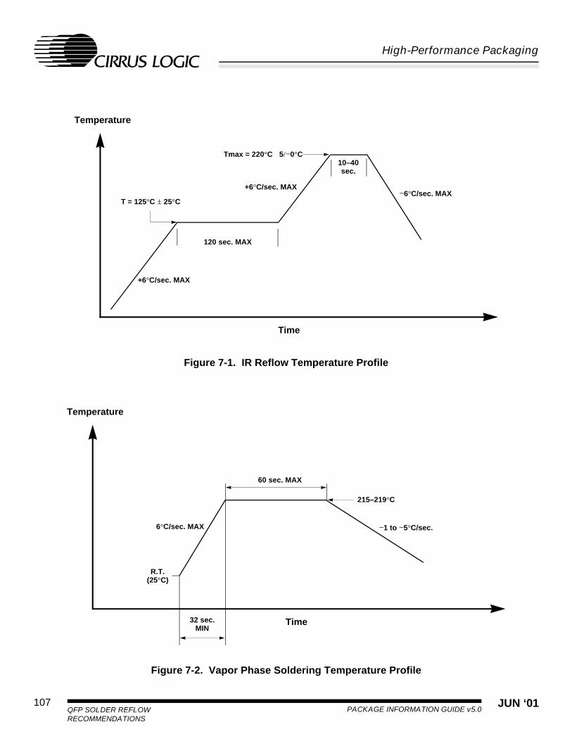
PACKAGE INFORMATION GUIDE v5.0JUN ‘01107
QFP SOLDER REFLOW RECOMMENDATIONS
High-Performance Packaging
Figure 7-1. IR Reflow Temperature Profile
Figure 7-2. Vapor Phase Soldering Temperature Profile
Temperature
Time
120 sec. MAX
T = 125°C ± 25°C −6°C/sec. MAX
10–40 sec.
Tmax = 220°C +5/−0°C
+6°C/sec. MAX
+6°C/sec. MAX
Time
60 sec. MAX
32 sec.MIN
215–219°C
R.T.(25°C)
6°C/sec. MAX −1 to −5°C/sec.
Temperature

JUN ‘01 108PACKAGE INFORMATION GUIDE v5.0 RELIABILITY TESTING SPECIFICATION
High-Performance Packaging
8. RELIABILITY TESTING SPECIFICATION8.1 Full Production Qualification (QPL II)—Sample Requirements
Qualification TestSuggested Sample
Size per LotNew Plastic
Package
New Hermetic Package
(Commercial)
New Hermetic Package(MIL 883)
Construction Analysis - Process 1 wafer – – –
Construction Analysis - Package 1 2 lots – –
Technology Stability N/A SPC Document SPC Document SPC Document
Physical Dimensions 5 3 lots – –
Infant Mortality 315 – – –
Early Life 154 – – –
Operating Life 77 – – –
Low Temperature Operating Life 100 – – –
Electrical Distribution (pre/post stress Cpk) 77 – – –
Moisture Resistance (THB) 77 3 lots – –
Autoclave Temperature Cycle 77 3 lots – –
Thermal Shock 77 3 lots 3 lots –
Thermal Sequence 15 – – 1 lot
Mechanical Sequence 77 3 lots 3 lots –
ESD - Human Body Model 5 – – 1 lot
ESD- Machine Model 5 – – –
Latch-up - I/O – – –
Latch-up - Power Supply 2 – – –
Internal Water Vapor 2 – – 1 lot
SEM Inspection/Metallization 3 – – 1 lot
Thermal Resistance 1 wafer Determine Determine Determine
Salt Atmosphere 1 – – 1 lot
Mark Permanency 5 – – –
Resistance to Solvents 5 3 lots 3 lots 1 lot
Lead Integrity 5 – – –
Lead Finish Adhesion 5 – 3 lots 1 lot
Lid Torque 5 – 3 lots 1 lot
Lead Pull and Lead Fatigue 5 3 lot – –
Solderability 5 3 lot 3 lots 1 lot
Solder Heat 5 3 lots (Non-SMD) 1 lot 1 lot
X-ray 5 3 Lots – –
Soak and Vapor Phase Reflow All Tests SMD – –

PACKAGE INFORMATION GUIDE v5.0JUN ‘01109
RELIABILITY TESTING SPECIFICATION
High-Performance Packaging
8.2 Qualification Criteria Summary by Level
Moisture Performance
Moisture resistance - THB (plastic packages) N/A 500/3% 1K/3% hours / %LTPD per lota
a LTPD and AQL criteria in table above apply to each lot tested. CUM LTPD and AQL numbers are also required for full production:
Individual Lot Cum Lot Requirement3% LTPD 1% LTPD2.5% AQL 1.0% AQL
Autoclave (plastic packages) N/A 96/3% 144/3% hours / %LTPD per lota
Mechanical Performance
Temperature cycle (plastic packages) N/A 500/3% 1K/3%b
b For surface-mount devices greater than 14 mm × 14 mm, the extended readings are for data collection purposes only.
#cy / %LTPD per lota
Thermal shock (plastic packages) N/A 200/3% 500/3%b #cy / %LTPD per lota
Temperature cycle with hermeticity (hermetic packages)
N/A 500/3% 1K/3%b #cy / %LTPD per lota
Thermal shock with hermeticity (hermetic packages)
N/A 200/3% 500/3%b #cy / %LTPD per lota
Soak and VPR/IR(surface mount plastic packages)
N/A 3/1% 3/1% #cy / %LTPD per lota
X-ray N/A 2.50% 2.50% %AQL per lota
Dimensions N/A 2.50% 2.50% %AQL per lota
Solderability N/A 2.50% 2.50% %AQL per lota
Lead integrity & lead pull N/A 2.50% 2.50% %AQL per lota
Scanning acoustic tomography N/A 2.50% 2.50% %AQL per lota
Mark permanency N/A 2.50% 2.50% %AQL per lota
Product Integrity
Design rule and LVS checks yes yes yes
Design for reliability and packaging yes yes yes
Product characterization initial limited full
Test guardbands some some 100%
Construction Analysis
Wafer cross section and topography N/A yes yes
SEM metallization N/A yes yes
Package N/A yes yes

JUN ‘01 110PACKAGE INFORMATION GUIDE v5.0 RELIABILITY TESTING SPECIFICATION
High-Performance Packaging
Notes

PACKAGE INFORMATION GUIDE v5.0JUN ‘01111
RELIABILITY TESTING SPECIFICATION
High-Performance Packaging
Notes

JUN ‘01 112PACKAGE INFORMATION GUIDE v5.0 RELIABILITY TESTING SPECIFICATION
High-Performance Packaging
Notes

Cirrus Logic, Inc. Publications Ordering: 800/359-6414 (USA)4210 S. Industrial Dr., Austin, TX 78744 Worldwide Web: http://www.cirrus.comTEL: 512/445-7222 FAX: 512/445-7581 939000-005
Package Information GuideVersion 5.0
Direct Sales Offices
High-Value Systems in Silicon
Cirrus Logic is a premier supplier of system-level integrated circuits that demand high-performance mixed-signal processing. Our company’s software-rich ‘systems in silicon’ add high value to major brands worldwide. We apply our system expertise to enable high-volume applications in data storage, networking, and multimedia for both computing and consumer electronics markets as well as ultra-high-precision data acquisition applications for industrial automation and instrumentation markets.
Cirrus Logic’s manufacturing strategy ensures maximum product quality and availability, as well as access to world-class processing technologies through joint ventures with IBM and Lucent Technologies.
Contact one of our systems and applications specialists to see how your company can benefit from the high value Cirrus Logic adds to its customers’ products.
Copyright 2001 Cirrus Logic, Inc. All rights reserved.
Cirrus Logic, Inc. has made best efforts to ensure that the information contained in this document is accurate and reliable. However, the information is subject tochange without notice. No responsibility is assumed by Cirrus Logic, Inc. for the use of this information, nor for infringements of patents or other rights of third parties.This document is the property of Cirrus Logic, Inc. and implies no license under patents, copyrights, or trade secrets. No part of this publication may be copied,reproduced, stored in a retrieval system or transmitted in any form or by any means (electronic, mechanical, photographic, or otherwise) or used as the basis formanufacture or sale of any items without the prior written consent of Cirrus Logic, Inc. Cirrus, Cirrus Logic, AccuPak, Alpine, Clear3D, Crystal, CrystalClear,CrystalWare, DirectVPM, DIVA, FastEn, FastPath, FasText, FeatureChips, FilterJet, Get into it, Good Data, IntelliFilter, Laguna, Laguna3D, LagunaTV, Matterhorn,MediaDAC, Mojave, MotionVideo, MVA, SimulSCAN, S/LA, SmartAnalog, SMASH, SofTarget, SoundFusion, Stargate, Systems in Silicon, TextureJet, True-D,TVTap, UXART, VisualMedia, VPM, V-Port, V-Port Manager, Voyager, WavePort, and WebSet are trademarks of Cirrus Logic, Inc., which may be registered in somejurisdictions. Other trademarks in this document belong to their respective companies. CRUS and Cirrus Logic International, Ltd. are trade names of Cirrus Logic, Inc.
Domestic
N. CALIFORNIAFremontTEL: 510/623-8300FAX: 510/252-6020
S. CALIFORNIAWestlake VillageTEL: 805/371-5860FAX: 805/371-5861
NORTHWESTERN AREAPortland, ORTEL: 503/620-5547FAX: 503/620-5665
SOUTH CENTRALAREAAustin, TXTEL: 512/255-0080FAX: 512/255-0733
Irving, TXTEL: 972/252-6698FAX: 972/252-5681
Houston, TXTEL: 281/257-2525FAX: 281/257-2555
NORTHEASTERN AREAAndover, MATEL: 978/794-9992FAX: 978/794-9998
SOUTHEASTERN AREARaleigh, NCTEL: 919/859-5210FAX: 919/859-5334
Boca Raton, FLTEL: 561/241-2364FAX: 561/241-7990
International
CHINABeijingTEL: 86/10-6428-0783FAX: 86/10-6428-0786
FRANCEParisTEL: 33/1-48-12-2812FAX: 33/1-48-12-2810
GERMANYHerrschingTEL: 49/81-52-92460FAX: 49/81-52-924699
HONG KONGTsimshatsuiTEL: 852/2376-0801FAX: 852/2375-1202
ITALYMilanTEL: 39/2-3360-5458FAX: 39/2-3360-5426
JAPANTokyoTEL: 81/3-3340-9111FAX: 81/3-3340-9120
KOREASeoulTEL: 82/2-565-8561FAX: 82/2-565-8565
SINGAPORETEL: 65/743-4111FAX: 65/742-4111
TAIWANTaipeiTEL: 886/2-2718-4533FAX: 886/2-2718-4526
UNITED KINGDOMLondon, EnglandTEL: 44/1727-872424FAX: 44/1727-875919