paralleling of igbt modules - abb group · paralleling of modules or paralleling of inverters...
TRANSCRIPT

Power and productivityfor a better world™
Paralleling of modules or paralleling of inverters becomes necessary, if a desired inverter rating or output current can not be achieved with a single IGBT module as switch. From an economic point of view paral-leling of modules is in many cases the solution of choice. On the other hand it is a technical challenging task to ensure proper current sharing between the parallel connected modules. This application note shades light on the technical measures which help to ensure a homogenous current sharing within the parallel connected power modules. Homogenous current sharing is also the key to maintain high ruggedness of the whole converter and it allows an optimal utilisation of the power modules with minimal de-rating.
Application Note 5SYA 2098-00
Paralleling of IGBT modules
2 Paralleling of IGBT modules I Application Note 5SYA 2098-00
Page
1 Introduction 3
2 Static current sharing 3 2.1 Influence of the module parameter spread 3 2.2 External influence on current sharing 4
3 Dynamic current sharing 4 3.1 Common Gate-Driver 4 3.2 Common Gate-Driver with common mode chokes 5 3.3 Individual Gate-Driver 6 3.4 Stray Inductance and Clamping 7 3.5 Phase connection 8 3.6 Influence of the junction Temperature 8 3.7 Influence of the device parameters 9
4 General recommendations / Summary 9 4.1 De-rating 9
5 References 9
Contents
3 Paralleling of IGBT modules I Application Note 5SYA 2098-00
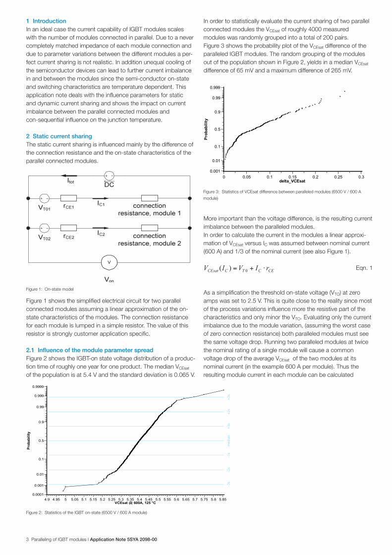
1 IntroductionIn an ideal case the current capability of IGBT modules scales with the number of modules connected in parallel. Due to a never completely matched impedance of each module connection and due to parameter variations between the different modules a per-fect current sharing is not realistic. In addition unequal cooling of the semiconductor devices can lead to further current imbalance in and between the modules since the semi-conductor on-state and switching characteristics are temperature dependent. This application note deals with the influence parameters for static and dynamic current sharing and shows the impact on current imbalance between the parallel connected modules and con-sequential influence on the junction temperature.
2 Static current sharingThe static current sharing is influenced mainly by the difference of the connection resistance and the on-state characteristics of the parallel connected modules.
Figure 1 shows the simplified electrical circuit for two parallel connected modules assuming a linear approximation of the on-state characteristics of the modules. The connection resistance for each module is lumped in a simple resistor. The value of this resistor is strongly customer application specific.
2.1 Influence of the module parameter spreadFigure 2 shows the IGBT-on state voltage distribution of a produc-tion time of roughly one year for one product. The median VCEsat of the population is at 5.4 V and the standard deviation is 0.065 V.
In order to statistically evaluate the current sharing of two parallel connected modules the VCEsat of roughly 4000 measured modules was randomly grouped into a total of 200 pairs.Figure 3 shows the probability plot of the VCEsat difference of the paralleled IGBT modules. The random grouping of the modules out of the population shown in Figure 2, yields in a median VCEsat difference of 65 mV and a maximum difference of 265 mV.
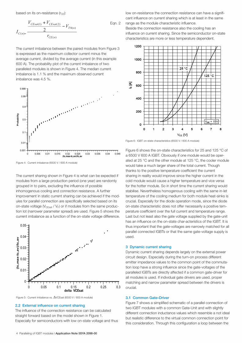
More important than the voltage difference, is the resulting current imbalance between the paralleled modules.In order to calculate the current in the modules a linear approxi-mation of VCEsat versus IC was assumed between nominal current (600 A) and 1/3 of the nominal current (see also Figure 1).
Eqn. 1
As a simplification the threshold on-state voltage (VTO) at zero amps was set to 2.5 V. This is quite close to the reality since most of the process variations influence more the resistive part of the characteristics and only minor the VTO. Evaluating only the current imbalance due to the module variation, (assuming the worst case of zero connection resistance) both paralleled modules must see the same voltage drop. Running two paralleled modules at twice the nominal rating of a single module will cause a common voltage drop of the average VCEsat of the two modules at its nominal current (in the example 600 A per module). Thus the resulting module current in each module can be calculated
Figure 1: On-state model
Figure 2: Statistics of the IGBT on-state (6500 V / 600 A module)
Figure 3: Statistics of VCEsat difference between paralleled modules (6500 V / 600 A
module)
0 0.05 0.1 0.15 0.2 0.25 0.3delta_VCEsat
0.001
0.01
0.1
0.5
0.9
0.99
0.999
Prob
abili
ty
4.9 4.95 5 5.05 5.1 5.15 5.2 5.25 5.3 5.35 5.4 5.45 5.5 5.55 5.6 5.65 5.7 5.75 5.8 5.85VCEsat @ 600A, 125 °C
0.0001
0.001
0.01
0.1
0.5
0.9
0.99
0.999
0.9999
Prob
abili
ty
+1s
-1s
+2s
-2s
+3s
-3s
med
ian
4 Paralleling of IGBT modules I Application Note 5SYA 2098-00
Eqn. 2
Figure 4: Current imbalance (6500 V / 600 A module)
based on its on-resistance (rCE):
The current imbalance between the paired modules from Figure 3 is expressed as the maximum collector current minus the average current, divided by the average current (in this example 600 A). The probability plot of the current imbalance of two paralleled modules is shown in Figure 4. The median current imbalance is 1.1 % and the maximum observed current imbalance was 4.5 %.
The current sharing shown in Figure 4 is what can be expected if modules from a large production period (one year) are randomly grouped in to pairs, excluding the influence of possible inhomogenous cooling and connection resistance. A further improvement in static current sharing can be achieved if the mod-ules for parallel connection are specifically selected based on its on-state voltage (VCEsat / VF) or if modules from the same produc-tion lot (narrower parameter spread) are used. Figure 5 shows the current imbalance as a function of the on-state voltage difference.
2.2 External influence on current sharingThe influence of the connection resistance can be calculated straight forward based on the model shown in Figure 1. Especially for semiconductors with low on-state voltage and thus
Figure 5: Current imbalance vs. VCEsat (6500 V / 600 A module)
0 0.005 0.01 0.015 0.02 0.025 0.03 0.035 0.04 0.045(Ic,max-Ic,av)/Ic,av
0.001
0.01
0.1
0.5
0.9
0.99
0.999
Pro
babi
lity
0 0.05 0.1 0.15 0.2 0.25 0.3delta_VCEsat
0
0.01
0.02
0.03
0.04
0.05
(Ic
,ma
x-I
c,a
v)/
Ic,a
vlow on-resistance the connection resistance can have a signifi-cant influence on current sharing which is at least in the same range as the module characteristic influence.Beside the connection resistance also the cooling has an influence on current sharing. Since the semiconductor on-state characteristics are more or less temperature dependent.
Figure 6 shows the on-state characteristics for 25 and 125 °C of a 6500 V 600 A IGBT. Obviously if one module would be oper-ated at 25 °C and the other module at 125 °C, the cooler module would take a much larger share of the total current. Though thanks to the positive temperature coefficient the current sharing in reality would improve since the higher current in the cold module would cause a higher temperature and vice versa for the hotter module. So in short time the current sharing would stabilise. Nevertheless homogenous cooling with the same in-let temperature of the cooling medium for both module heat-sinks is crucial. Especially for the diode operation mode, since the diode on-state characteristic does not offer necessarily a positive tem-perature coefficient over the full current and temperature range.Last but not least also the gate voltage supplied by the gate-unit has an influence on the on-state char-acteristics of the IGBT. It is thus important that the gate-voltages are narrowly matched for all parallel connected IGBTs or that the same gate-voltage supply is used.
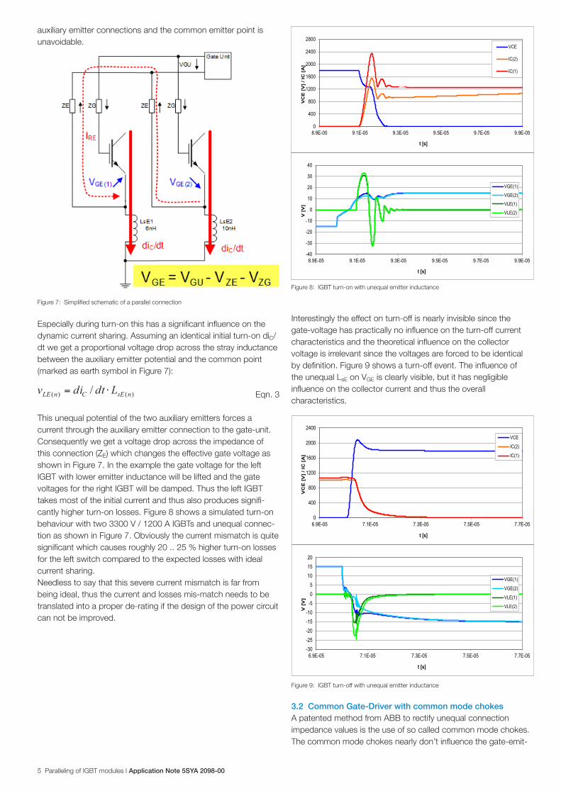
3 Dynamic current sharingDynamic current sharing depends largely on the external power circuit design. Especially during the turn-on process different emitter impedance values to the common point of the commuta-tion loop have a strong influence since the gate-voltages of the paralleled IGBTs are directly affected if a common gate-driver for all modules is used. If individual gate drivers are used, proper matching and narrow parameter spread between the drivers is crucial.
3.1 Common Gate-DriverFigure 7 shows a simplified schematic of a parallel connection of two IGBT modules with a common Gate-Unit and with slightly different connection inductance values which resemble a not ideal but realistic difference to the virtual common connection point for this consideration. Through this configuration a loop between the
Figure 6: IGBT on-state characteristics (6500 V / 600 A module)
5 Paralleling of IGBT modules I Application Note 5SYA 2098-00
Figure 7: Simplified schematic of a parallel connection
auxiliary emitter connections and the common emitter point is unavoidable.
Especially during turn-on this has a significant influence on the dynamic current sharing. Assuming an identical initial turn-on diC/dt we get a proportional voltage drop across the stray inductance between the auxiliary emitter potential and the common point (marked as earth symbol in Figure 7):
Eqn. 3
This unequal potential of the two auxiliary emitters forces a current through the auxiliary emitter connection to the gate-unit. Consequently we get a voltage drop across the impedance of this connection (ZE) which changes the effective gate voltage as shown in Figure 7. In the example the gate voltage for the left IGBT with lower emitter inductance will be lifted and the gate voltages for the right IGBT will be damped. Thus the left IGBT takes most of the initial current and thus also produces signifi-cantly higher turn-on losses. Figure 8 shows a simulated turn-on behaviour with two 3300 V / 1200 A IGBTs and unequal connec-tion as shown in Figure 7. Obviously the current mismatch is quite significant which causes roughly 20 .. 25 % higher turn-on losses for the left switch compared to the expected losses with ideal current sharing.Needless to say that this severe current mismatch is far from being ideal, thus the current and losses mis-match needs to be translated into a proper de-rating if the design of the power circuit can not be improved.
Interestingly the effect on turn-off is nearly invisible since the gate-voltage has practically no influence on the turn-off current characteristics and the theoretical influence on the collector voltage is irrelevant since the voltages are forced to be identical by definition. Figure 9 shows a turn-off event. The influence of the unequal LsE on VGE is clearly visible, but it has negligible influence on the collector current and thus the overall characteristics.
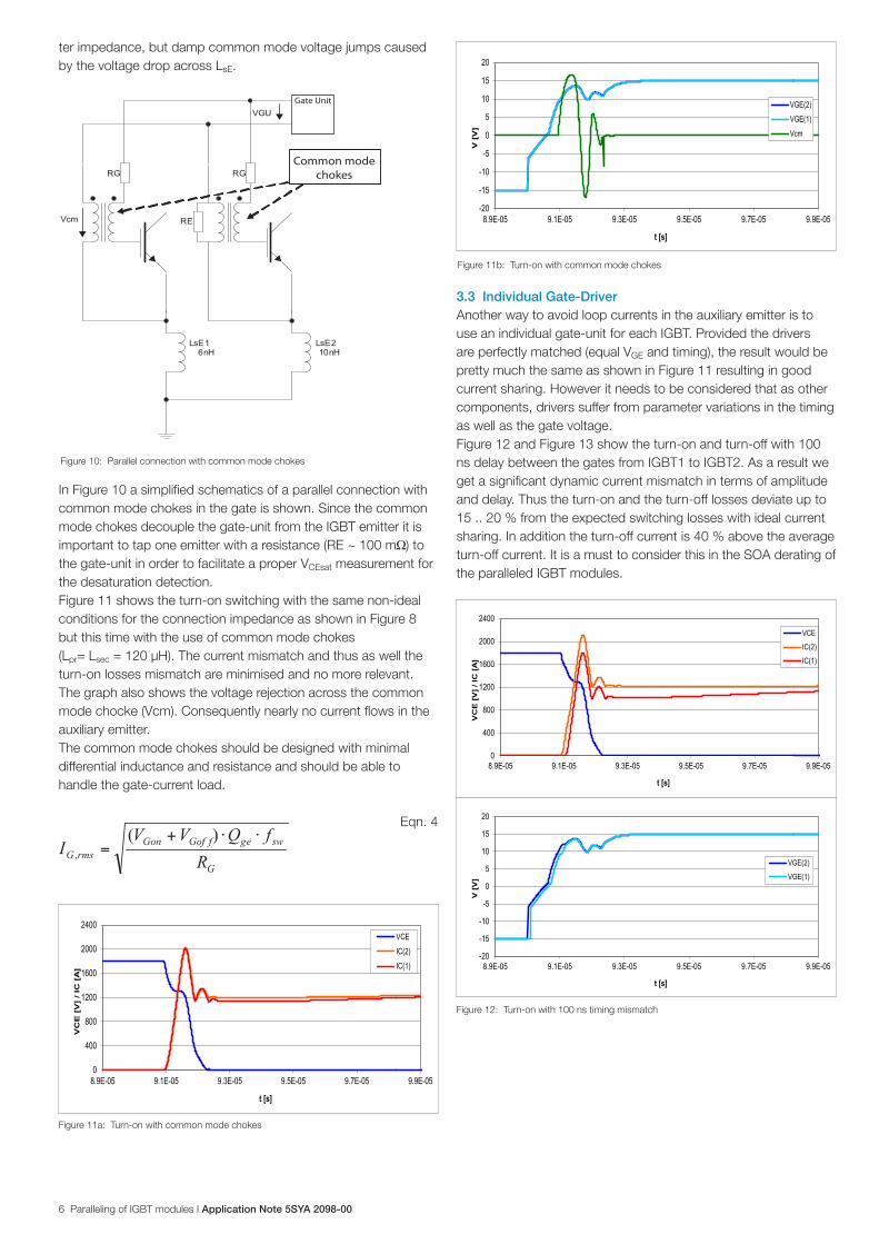
3.2 Common Gate-Driver with common mode chokesA patented method from ABB to rectify unequal connection impedance values is the use of so called common mode chokes. The common mode chokes nearly don’t influence the gate-emit-
Figure 8: IGBT turn-on with unequal emitter inductance
Figure 9: IGBT turn-off with unequal emitter inductance
0
400
800
1200
1600
2000
2400
2800
8.9E-05 9.1E-05 9.3E-05 9.5E-05 9.7E-05 9.9E-05
VC
E [
V]
/ IC
[A
]
t [s]
VCE
IC(2)
IC(1)
-40
-30
-20
-10
0
10
20
30
40
8.9E-05 9.1E-05 9.3E-05 9.5E-05 9.7E-05 9.9E-05
V [
V]
t [s]
VGE(1)
VGE(2)
VLE(1)
VLE(2)
0
400
800
1200
1600
2000
2400
6.9E-05 7.1E-05 7.3E-05 7.5E-05 7.7E-05
VC
E [
V]
/ IC
[A
]
t [s]
VCE
IC(2)
IC(1)
-30-25-20-15-10-505
101520
6.9E-05 7.1E-05 7.3E-05 7.5E-05 7.7E-05
V [
V]
t [s]
VGE(1)
VGE(2)
VLE(1)
VLE(2)
6 Paralleling of IGBT modules I Application Note 5SYA 2098-00
Figure 10: Parallel connection with common mode chokes
Figure 11a: Turn-on with common mode chokes
ter impedance, but damp common mode voltage jumps caused by the voltage drop across LsE.
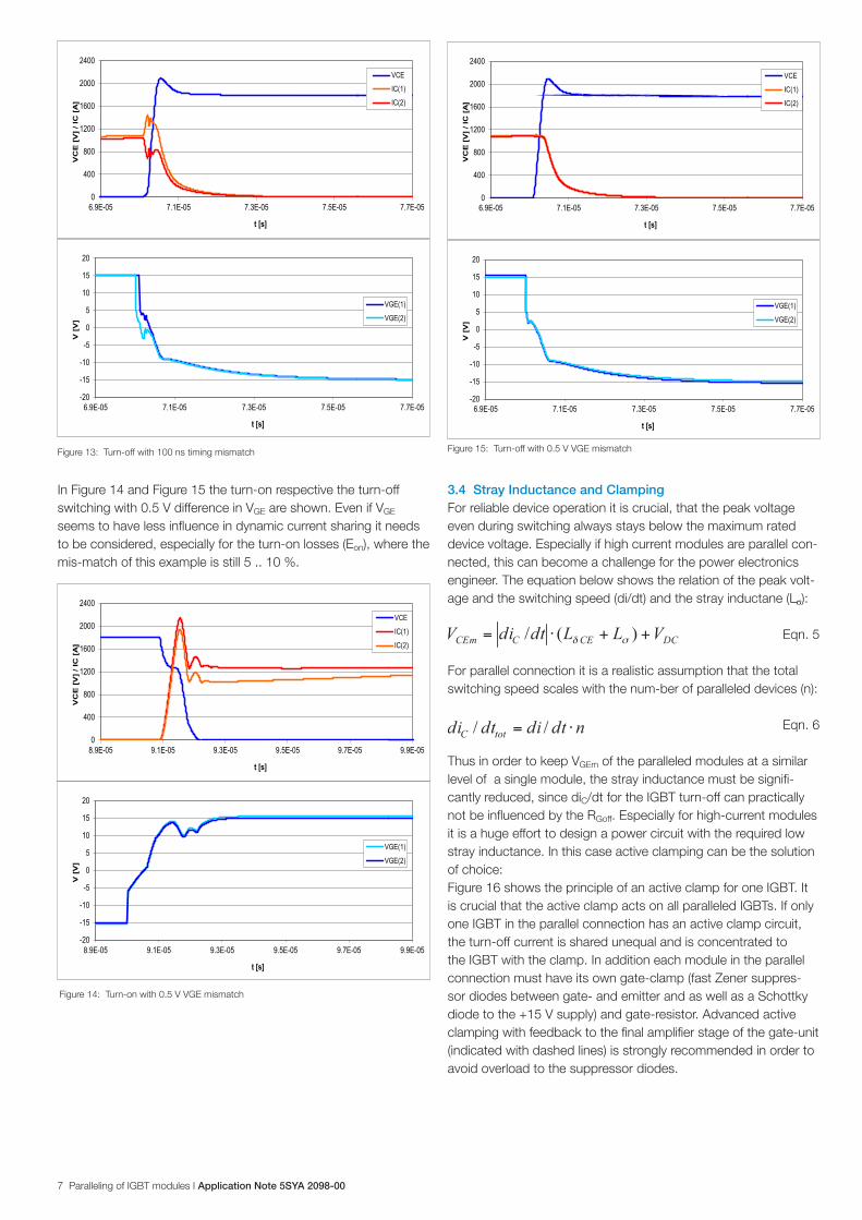
In Figure 10 a simplified schematics of a parallel connection with common mode chokes in the gate is shown. Since the common mode chokes decouple the gate-unit from the IGBT emitter it is important to tap one emitter with a resistance (RE ~ 100 m ) to the gate-unit in order to facilitate a proper VCEsat measurement for the desaturation detection.Figure 11 shows the turn-on switching with the same non-ideal conditions for the connection impedance as shown in Figure 8 but this time with the use of common mode chokes (Lpr= Lsec = 120 µH). The current mismatch and thus as well the turn-on losses mismatch are minimised and no more relevant. The graph also shows the voltage rejection across the common mode chocke (Vcm). Consequently nearly no current flows in the auxiliary emitter.The common mode chokes should be designed with minimal differential inductance and resistance and should be able to handle the gate-current load.
Eqn. 4
Figure 11b: Turn-on with common mode chokes
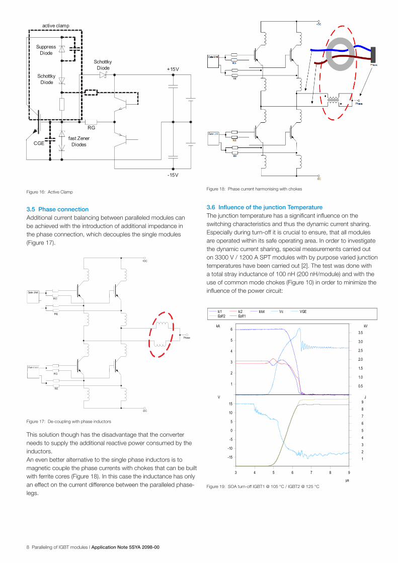
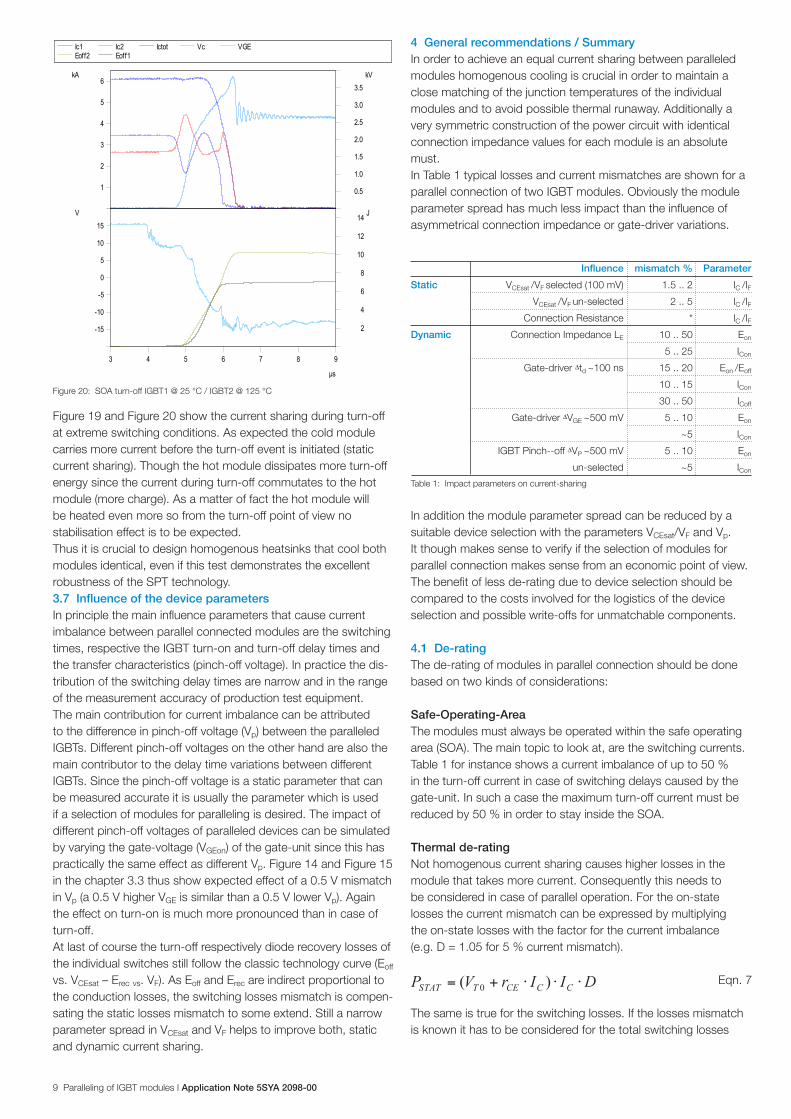
3.3 Individual Gate-DriverAnother way to avoid loop currents in the auxiliary emitter is to use an individual gate-unit for each IGBT. Provided the drivers are perfectly matched (equal VGE and timing), the result would be pretty much the same as shown in Figure 11 resulting in good current sharing. However it needs to be considered that as other components, drivers suffer from parameter variations in the timing as well as the gate voltage. Figure 12 and Figure 13 show the turn-on and turn-off with 100 ns delay between the gates from IGBT1 to IGBT2. As a result we get a significant dynamic current mismatch in terms of amplitude and delay. Thus the turn-on and the turn-off losses deviate up to 15 .. 20 % from the expected switching losses with ideal current sharing. In addition the turn-off current is 40 % above the average turn-off current. It is a must to consider this in the SOA derating of the paralleled IGBT modules.
Figure 12: Turn-on with 100 ns timing mismatch
0
400
800
1200
1600
2000
2400
8.9E-05 9.1E-05 9.3E-05 9.5E-05 9.7E-05 9.9E-05
VC
E [
V]
/ IC
[A
]
t [s]
VCE
IC(2)
IC(1)
-20
-15
-10
-5
0
5
10
15
20
8.9E-05 9.1E-05 9.3E-05 9.5E-05 9.7E-05 9.9E-05
V [
V]
t [s]
VGE(2)
VGE(1)
Vcm
0
400
800
1200
1600
2000
2400
8.9E-05 9.1E-05 9.3E-05 9.5E-05 9.7E-05 9.9E-05
VC
E [
V]
/ IC
[A
]
t [s]
VCE
IC(2)
IC(1)
-20
-15
-10
-5
0
5
10
15
20
8.9E-05 9.1E-05 9.3E-05 9.5E-05 9.7E-05 9.9E-05
V [
V]
t [s]
VGE(2)
VGE(1)
7 Paralleling of IGBT modules I Application Note 5SYA 2098-00
Figure 13: Turn-off with 100 ns timing mismatch
Figure 14: Turn-on with 0.5 V VGE mismatch
Figure 15: Turn-off with 0.5 V VGE mismatch
In Figure 14 and Figure 15 the turn-on respective the turn-off switching with 0.5 V difference in VGE are shown. Even if VGE seems to have less influence in dynamic current sharing it needs to be considered, especially for the turn-on losses (Eon), where the mis-match of this example is still 5 .. 10 %.
3.4 Stray Inductance and ClampingFor reliable device operation it is crucial, that the peak voltage even during switching always stays below the maximum rated device voltage. Especially if high current modules are parallel con-nected, this can become a challenge for the power electronics engineer. The equation below shows the relation of the peak volt-age and the switching speed (di/dt) and the stray inductane (L ):
Eqn. 5
For parallel connection it is a realistic assumption that the total switching speed scales with the num-ber of paralleled devices (n): Eqn. 6
Thus in order to keep VGEm of the paralleled modules at a similar level of a single module, the stray inductance must be signifi-cantly reduced, since diC/dt for the IGBT turn-off can practically not be influenced by the RGoff. Especially for high-current modules it is a huge effort to design a power circuit with the required low stray inductance. In this case active clamping can be the solution of choice: Figure 16 shows the principle of an active clamp for one IGBT. It is crucial that the active clamp acts on all paralleled IGBTs. If only one IGBT in the parallel connection has an active clamp circuit, the turn-off current is shared unequal and is concentrated to the IGBT with the clamp. In addition each module in the parallel connection must have its own gate-clamp (fast Zener suppres-sor diodes between gate- and emitter and as well as a Schottky diode to the +15 V supply) and gate-resistor. Advanced active clamping with feedback to the final amplifier stage of the gate-unit (indicated with dashed lines) is strongly recommended in order to avoid overload to the suppressor diodes.
0
400
800
1200
1600
2000
2400
6.9E-05 7.1E-05 7.3E-05 7.5E-05 7.7E-05
VC
E [
V]
/ IC
[A
]
t [s]
VCE
IC(1)
IC(2)
-20
-15
-10
-5
0
5
10
15
20
6.9E-05 7.1E-05 7.3E-05 7.5E-05 7.7E-05
V [
V]
t [s]
VGE(1)
VGE(2)
0
400
800
1200
1600
2000
2400
8.9E-05 9.1E-05 9.3E-05 9.5E-05 9.7E-05 9.9E-05
VC
E [
V]
/ IC
[A
]
t [s]
VCE
IC(1)
IC(2)
-20
-15
-10
-5
0
5
10
15
20
8.9E-05 9.1E-05 9.3E-05 9.5E-05 9.7E-05 9.9E-05
V [
V]
t [s]
VGE(1)
VGE(2)
0
400
800
1200
1600
2000
2400
6.9E-05 7.1E-05 7.3E-05 7.5E-05 7.7E-05
VC
E [
V]
/ IC
[A
]
t [s]
VCE
IC(1)
IC(2)
-20
-15
-10
-5
0
5
10
15
20
6.9E-05 7.1E-05 7.3E-05 7.5E-05 7.7E-05
V [
V]
t [s]
VGE(1)
VGE(2)
8 Paralleling of IGBT modules I Application Note 5SYA 2098-00
Figure 16: Active Clamp
Figure 17: De-coupling with phase inductors
Figure 18: Phase current harmonising with chokes
Figure 19: SOA turn-off IGBT1 @ 105 °C / IGBT2 @ 125 °C
3.5 Phase connectionAdditional current balancing between paralleled modules can be achieved with the introduction of additional impedance in the phase connection, which decouples the single modules (Figure 17).
This solution though has the disadvantage that the converter needs to supply the additional reactive power consumed by the inductors. An even better alternative to the single phase inductors is to magnetic couple the phase currents with chokes that can be built with ferrite cores (Figure 18). In this case the inductance has only an effect on the current difference between the paralleled phase-legs.
3.6 Influence of the junction TemperatureThe junction temperature has a significant influence on the switching characteristics and thus the dynamic current sharing. Especially during turn-off it is crucial to ensure, that all modules are operated within its safe operating area. In order to investigate the dynamic current sharing, special measurements carried out on 3300 V / 1200 A SPT modules with by purpose varied junction temperatures have been carried out [2]. The test was done with a total stray inductance of 100 nH (200 nH/module) and with the use of common mode chokes (Figure 10) in order to minimize the influence of the power circuit:
Ic1 Ic2 Ictot Vc VGEEoff2 Eoff1
1
2
3
4
5
6kA
0.5
1.0
1.5
2.0
2.5
3.0
3.5kV
-15
-10
-5
0
5
10
15V
1
2
3
4
5
6
7
8
9J
3 4 5 6 7 8 9
µs
9 Paralleling of IGBT modules I Application Note 5SYA 2098-00
Figure 20: SOA turn-off IGBT1 @ 25 °C / IGBT2 @ 125 °C
Figure 19 and Figure 20 show the current sharing during turn-off at extreme switching conditions. As expected the cold module carries more current before the turn-off event is initiated (static current sharing). Though the hot module dissipates more turn-off energy since the current during turn-off commutates to the hot module (more charge). As a matter of fact the hot module will be heated even more so from the turn-off point of view no stabilisation effect is to be expected. Thus it is crucial to design homogenous heatsinks that cool both modules identical, even if this test demonstrates the excellent robustness of the SPT technology.3.7 Influence of the device parametersIn principle the main influence parameters that cause current imbalance between parallel connected modules are the switching times, respective the IGBT turn-on and turn-off delay times and the transfer characteristics (pinch-off voltage). In practice the dis-tribution of the switching delay times are narrow and in the range of the measurement accuracy of production test equipment. The main contribution for current imbalance can be attributed to the difference in pinch-off voltage (Vp) between the paralleled IGBTs. Different pinch-off voltages on the other hand are also the main contributor to the delay time variations between different IGBTs. Since the pinch-off voltage is a static parameter that can be measured accurate it is usually the parameter which is used if a selection of modules for paralleling is desired. The impact of different pinch-off voltages of paralleled devices can be simulated by varying the gate-voltage (VGEon) of the gate-unit since this has practically the same effect as different Vp. Figure 14 and Figure 15 in the chapter 3.3 thus show expected effect of a 0.5 V mismatch in Vp (a 0.5 V higher VGE is similar than a 0.5 V lower Vp). Again the effect on turn-on is much more pronounced than in case of turn-off.At last of course the turn-off respectively diode recovery losses of the individual switches still follow the classic technology curve (Eoff vs. VCEsat – Erec vs. VF). As Eoff and Erec are indirect proportional to the conduction losses, the switching losses mismatch is compen-sating the static losses mismatch to some extend. Still a narrow parameter spread in VCEsat and VF helps to improve both, static and dynamic current sharing.
Influence mismatch % Parameter
Static VCEsat /VF selected (100 mV) 1.5 .. 2 IC /IF VCEsat /VF un-selected 2 .. 5 IC /IF Connection Resistance * IC /IFDynamic Connection Impedance LE 10 .. 50 Eon
5 .. 25 ICon
Gate-driver td ~100 ns 15 .. 20 Eon /Eoff
10 .. 15 ICon
30 .. 50 ICoff
Gate-driver VGE ~500 mV 5 .. 10 Eon
~5 ICon
IGBT Pinch--off VP ~500 mV 5 .. 10 Eon
un-selected ~5 ICon
Table 1: Impact parameters on current-sharing
Ic1 Ic2 Ictot Vc VGEEoff2 Eoff1
1
2
3
4
5
6kA
0.5
1.0
1.5
2.0
2.5
3.0
3.5kV
-15
-10
-5
0
5
10
15V
2
4
6
8
10
12
14 J
3 4 5 6 7 8 9
µs
4 General recommendations / SummaryIn order to achieve an equal current sharing between paralleled modules homogenous cooling is crucial in order to maintain a close matching of the junction temperatures of the individual modules and to avoid possible thermal runaway. Additionally a very symmetric construction of the power circuit with identical connection impedance values for each module is an absolute must.In Table 1 typical losses and current mismatches are shown for a parallel connection of two IGBT modules. Obviously the module parameter spread has much less impact than the influence of asymmetrical connection impedance or gate-driver variations.
In addition the module parameter spread can be reduced by a suitable device selection with the parameters VCEsat/VF and Vp. It though makes sense to verify if the selection of modules for parallel connection makes sense from an economic point of view. The benefit of less de-rating due to device selection should be compared to the costs involved for the logistics of the device selection and possible write-offs for unmatchable components.
4.1 De-ratingThe de-rating of modules in parallel connection should be done based on two kinds of considerations:
Safe-Operating-AreaThe modules must always be operated within the safe operating area (SOA). The main topic to look at, are the switching currents. Table 1 for instance shows a current imbalance of up to 50 % in the turn-off current in case of switching delays caused by the gate-unit. In such a case the maximum turn-off current must be reduced by 50 % in order to stay inside the SOA.
Thermal de-ratingNot homogenous current sharing causes higher losses in the module that takes more current. Consequently this needs to be considered in case of parallel operation. For the on-state losses the current mismatch can be expressed by multiplying the on-state losses with the factor for the current imbalance (e.g. D = 1.05 for 5 % current mismatch).
Eqn. 7
The same is true for the switching losses. If the losses mismatch is known it has to be considered for the total switching losses
Power and productivityfor a better world™
App
licat
ion
note
5S
YA 2
098-
00
25.
08.2
013
NoteWe reserve the right to make technical changesor to modify the contents of this documentwithout prior notice.We reserve all rights in this document and theinformation contained therein. Any reproductionor utilisation of this document or parts thereof forcommercial purposes without our prior writtenconsent is forbidden.Any liability for use of our products contrary to theinstructions in this document is excluded.
ABB Switzerland Ltd.SemiconductorsFabrikstrasse 3CH-5600 LenzburgSwitzerlandTel: +41 58 586 14 19Fax: +41 58 586 13 06E-Mail: [email protected]/semiconductors
Eqn. 8
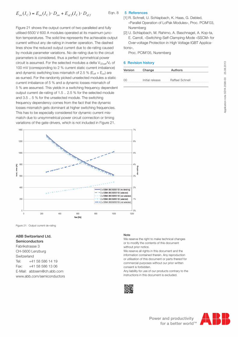
Figure 21 shows the output current of two paralleled and fully utilised 6500 V 600 A modules operated at its maximum junc-tion temperatures. The solid line represents the achievable output current without any de-rating in inverter operation. The dashed lines show the reduced output current due to de-rating caused by module parameter variations. No de-rating due to the circuit parameters is considered, thus a perfect symmetrical power circuit is assumed. For the selected modules a delta VCEsat/VF of 100 mV (corresponding to 2 % current static current imbalance) and dynamic switching loss mismatch of 2.5 % (Eoff + Eon) are as-sumed. For the randomly picked unselected modules a static current imbalance of 5 % and a dynamic losses mismatch of 5 % are assumed. This yields in a switching frequency dependent output current de-rating of 1.5 .. 2.5 % for the selected module and 3.5 .. 5 % for the unselected module. The switching frequency dependency comes from the fact that the dynamic losses mismatch gets dominant at higher switching frequencies. This has to be especially considered for dynamic current mis-match due to unsymmetrical power circuit connection or timing variations of the gate-drivers, which is not included in Figure 21.
Figure 21: Output current de-rating
Version Change Authors
00 Initial release Raffael Schnell
5 References[1] R. Schnell, U. Schlapbach, K. Haas, G. Debled, «Parallel Operation of LoPak Modules», Proc. PCIM’03, Nuremberg[2] U. Schlapbach, M. Rahimo, A. Baschnagel, A. Kop-ta, E. Carroll, «Switching-Self-Clamping-Mode «SSCM» for Over-voltage Protection in High Voltage IGBT Applica-tions», Proc. PCIM’05, Nuremberg
6 Revision history