paralleling power mosfets in high power applications
TRANSCRIPT

AN50005Paralleling power MOSFETs in high power applicationsRev. 1.1 — 13 September 2021 application note
Document informationInformation Content
Keywords MOSFETs, paralleling, parameter spread, simulation
Abstract This application note examines how current sharing imbalances between paralleled MOSFETsare affected by various parameters. Guidelines are given on taking these into account in designs.Realistic descriptions are provided to help designers to develop reliable and cost effective highpower solutions.

Nexperia AN50005Paralleling power MOSFETs in high power applications
1. IntroductionIn today’s automotive and power industries, higher power requirements are leading to moredesigns that require lower RDSon. Sometimes this is not achievable with a single packagedMOSFET and the design will need to make use of two or more devices in parallel. Higher powerapplications could also require the use of high performance substrates like heavy copper PCB, IMS(Insulated Metal Substrate) or DBC (Direct Bonded Copper) and even bare dies. By paralleling, thetotal current and thus dissipation is shared between each device. However, this is not as simple asapplying Kirchhoff’s current law: MOSFETs are not identical and thus they don’t share equally.
This application note describes how sharing imbalances between paralleled MOSFETs form as wellas guidelines and tools to take them into account. The final goal is to provide a set of best practicesthat can help to design circuits with standard paralleled MOSFETs.
2. ApplicationsApplications that require paralleled MOSFETs can be categorized into two main groups dependingon the operation of the MOSFET: switch-mode and load switch.
The switch-mode types include motor drive applications, such as belt starter generators andsuperchargers, braking regeneration systems and switched mode power converters, such asregulators (DC/DC) and other types of inverters (DC/AC). Here the half-bridge represents thefundamental cell block that all the major circuit topologies are based upon. The MOSFETs aregenerally required to switch ON and OFF at a constant rate that can vary widely depending on theapplication, and are driven by a rectangular pulse with varying duty cycle (PWM). This is done withthe intent of modulating the output power of the system to the load.
Load switching mainly refers to applications where MOSFETs are used in series with the batterysuch as in activation, safety switches and e-fuses, one example being battery isolation switches.The MOSFETs are required to switch ON once and will remain fully ON until the system is switchedOFF. They might be swiftly switched OFF only in case some type of failure has been detected,for example in case of short circuit. Additionally, these switches may come in a back-to-backconfiguration in order to offer an additional reverse polarity protection.
This application note focuses on switch-mode applications and the half-bridge configuration.
3. Key specificationsThe most important figure to monitor is the MOSFET junction temperature. This is a function ofthe power dissipated in each device which ideally should be uniform for all paralleled MOSFETs.Since P = V × I and the same voltage is applied across all the paralleled MOSFETs, it is clearthat for ideal operation the current should be shared equally by each MOSFET and this is thesimplest metric to quantify how well the MOSFETs perform. However, an equally valid approachis to consider the dissipated energy (or power), as done throughout the majority of this applicationnote.
Current sharing in paralleled MOSFETs is mainly affected by the part to part variation of threedata sheet parameters: RDSon, QG(tot), and VGS(th). This will be described further in the appropriatesections.
During the design phase, it is important to understand how to predict the worst case scenarioin part to part variation in order to produce a reliable design. As with many other aspects ofelectronics, the designer will eventually decide how much of a headroom to adopt against theaforementioned worst case, maybe trading off some of the design robustness for improvedperformance. As better said in “The Art of Electronics”:
"This example illustrates a frequent designer’s quandary, namely a choice between aconservative circuit that meets the strict worst-case design criterion, and is therefore
guaranteed to work, and a better-performing circuit design that does not meet worst-casespecifications, but is overwhelmingly likely to function without problems. There are times whenyou will find yourself choosing the latter, ignoring the little voice whispering into your ear." [1]
AN50005 All information provided in this document is subject to legal disclaimers. © Nexperia B.V. 2021. All rights reserved
application note Rev. 1.1 — 13 September 2021 2 / 41

Nexperia AN50005Paralleling power MOSFETs in high power applications
Simulation setupDisclaimer: this application note proposes the alteration of SPICE models. It is the user’sresponsibility to verify the model conformity to the data sheet, after any modification hasbeen implemented. This can be done by following the guidelines described in the appendix.
The circuit used in the application note is composed of 3 MOSFETs in parallel both at the high andlow side driving an inductive load, as shown in Fig. 1. The switching frequency is set at 20 kHz,duty cycle at 50 % and maximum VGS is 15 V. Each MOSFET is conducting a current of 50 A,which is set by the constant current source of 150 A used in series with the load inductor. TheSPICE simulation contains also three 0 V generators, one in each low side MOSFET source path,which are used to measure the low side drain current in order to calculate the dissipated energyand power. BUK7S1R0-40H is used throughout this document, unless stated otherwise. As shownin Fig. 1, parasitic inductance linked to the layout has been added to the simulation. There is nodifference in terms of parasitics between the three branches (each branch corresponds to a singleMOSFET and the path connecting it to the others in parallel through inlet and outlet: VSUPPLY andphase for the high side, phase and GND for the low side).
This is an ideal scenario but achievable in practice within a reasonable margin. In this case anyimbalance will only be determined by the intrinsic differences between the MOSFETs themselves.The importance of layout and influence of parasitics is discussed further in the correspondingchapter.
It is worth noting that the guidelines and observations made from now on do not depend on thebattery voltage or other specifications, so they can be applied to a wide range of scenarios.
aaa-033634
Rsupply
Vsupply
LB
L1Vp
RB
CB
R11 kΩ
B1
V=(V(Vd1)-V(Vs1))*I(VM1)
Pdiss1
BL
V=V(VgsLS)
VM1
0 V
R21 kΩ
B2
V=(V(Vd2)-V(Vs2))*I(VM2)
Pdiss2
R51 kΩ
Rgdrv2
12 Ω
Rg1 M1BUK7S1R0-40H
L14Vd1
Vs13.9 Ω
Rg2 L15
3.9 Ω
Rg3 L16
L17
VM2
0 V
M2BUK7S1R0-40H
Vd2
Vs2
L18
VM3
0 V
M3BUK7S1R0-40H
Vd3
Vs3
L19
L11 L12 L13
L8 L9 L10
3.9 Ω
BH
V=V(VgsHS)
Iload
150 A
Rgdrv1
12 Ω
Rg4 M4BUK7S1R0-40H
L5
3.9 Ω
Rg5 L6
3.9 Ω
Rg6 L7
Lload4 µH
M5BUK7S1R0-40H
M6BUK7S1R0-40H
L2 L3 L4
3.9 Ω
B5
V=∫Pdiss2*dt
Ediss2
R41 kΩ
B4
V=∫Pdiss1*dt
Ediss1
R31 kΩ
B3
V=(V(Vd3)-V(Vs3))*I(VM3)
Pdiss3
R61 kΩ
B6
V=∫Pdiss3*dt
Ediss3
Fig. 1. SPICE simulation circuit: half-bridge
AN50005 All information provided in this document is subject to legal disclaimers. © Nexperia B.V. 2021. All rights reserved
application note Rev. 1.1 — 13 September 2021 3 / 41
Nexperia AN50005Paralleling power MOSFETs in high power applications
4. MOSFET dissipation and parameters' influence on current sharingBy understanding how MOSFET dissipation works and highlighting which are the main parametersaffecting it, it is possible to steer the worst case analysis towards a less burdensome but stillrealistic evaluation.
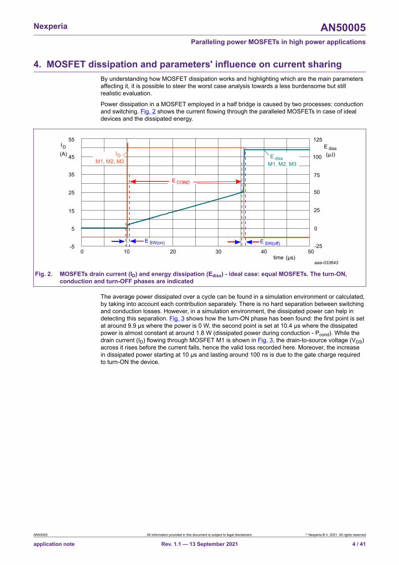
Power dissipation in a MOSFET employed in a half bridge is caused by two processes: conductionand switching. Fig. 2 shows the current flowing through the paralleled MOSFETs in case of idealdevices and the dissipated energy.
I(A)
D
15
-5
5
45
55
35
25
time (µs)0 10 20 30 40 50
aaa-033643
E(µJ)
diss
25
-25
0
100
125
75
50
M1, M2, M3ID
M1, M2, M3E diss
E COND
E SW(on) E SW(off)
Fig. 2. MOSFETs drain current (ID) and energy dissipation (Ediss) - ideal case: equal MOSFETs. The turn-ON,conduction and turn-OFF phases are indicated
The average power dissipated over a cycle can be found in a simulation environment or calculated,by taking into account each contribution separately. There is no hard separation between switchingand conduction losses. However, in a simulation environment, the dissipated power can help indetecting this separation. Fig. 3 shows how the turn-ON phase has been found: the first point is setat around 9.9 µs where the power is 0 W, the second point is set at 10.4 µs where the dissipatedpower is almost constant at around 1.8 W (dissipated power during conduction - Pcond). While thedrain current (ID) flowing through MOSFET M1 is shown in Fig. 3, the drain-to-source voltage (VDS)across it rises before the current falls, hence the valid loss recorded here. Moreover, the increasein dissipated power starting at 10 μs and lasting around 100 ns is due to the gate charge requiredto turn-ON the device.
AN50005 All information provided in this document is subject to legal disclaimers. © Nexperia B.V. 2021. All rights reserved
application note Rev. 1.1 — 13 September 2021 4 / 41

Nexperia AN50005Paralleling power MOSFETs in high power applications
I(A)
D
15
-5
5
45
55
35
25
time (µs)9.6 10 10.4 10.8 11.2
aaa-033730
M1ID
M1E dissE SW(on)
P
(W)diss
30
-10
10
90
110
70
50
3
-1
1
11
7
(µJ)diss
E
9
5
M1P diss
PCOND
Fig. 3. MOSFETs drain current (ID), energy dissipation (Ediss) and power dissipation (Pdiss)- ideal case: equal MOSFETs. The turn-ON phase is indicated
Fig. 4 shows how the turn-OFF phase has been found: the first point is set at 36.2 µs where thepower is 0 W, the second point is set at around 35.2 µs where the dissipated power starts toincrease from 1.8 W.
I(A)
D
15
-5
5
45
55
35
25
time (µs)34.6 35 35.4 36.2 36.6
aaa-033731
P
(W)diss
300
-100
100
900
1100
700
500
40
-20
20
100
(µJ)diss
E
120
80E SW(OFF)
35.8
M1P diss
PCOND
M1E diss
M1ID
60
Fig. 4. MOSFETs drain current (ID), energy dissipation (Ediss) and power dissipation (Pdiss)- ideal case: equal MOSFETs. The turn-OFF phase is indicated
Equation 1 expresses the power dissipation in the MOSFET, while equations 2 and 3 show theindividual contributions from switching and conduction.
P =avg(tot) Psw + Pcond (1)
(E=Psw + f swsw(ON) Esw(OFF)) (2)
E= f swPcond cond (3)
Where Esw(ON) and Esw(OFF) are the energy dissipation during turn-ON and turn-OFF, Econd isthe energy dissipation during a single conduction phase and fsw the switching frequency. In thiscase, the total average power dissipated across each MOSFET over one cycle is around 2.1 W at20 kHz.
AN50005 All information provided in this document is subject to legal disclaimers. © Nexperia B.V. 2021. All rights reserved
application note Rev. 1.1 — 13 September 2021 5 / 41

Nexperia AN50005Paralleling power MOSFETs in high power applications
Table 1 shows the energy calculated during switching (divided into ON and OFF) and conduction.The degree of sharing of each MOSFET can be defined in several ways. Here it is defined asratio between the energy dissipated in one MOSFET and the total energy dissipated in all of theparalleled devices, by using equation 4.
Total Energy Sharing n FET
ESW(ON)=
Σ i =1
+ ESW(OFF)+ E SW(COND) (Mx) 100( (
(Mi)ESW(ON) + ESW(OFF)+ E SW(COND)( ( (4)
In this case, switching (Esw(ON) + Esw(OFF)) accounts for around 55 % of the overall dissipation.However the switching:conduction dissipation ratio will depend on the switching frequency: a lowfrequency will lead to conduction losses dominating whereas switching losses will dominate at highfrequency. Therefore, in order to simplify the evaluation, one might consider to take into accountonly parameters influencing the most important contribution.
With the MOSFET fully ON the only source of dissipation is given by its drain-to-source on stateresistance (RDSon). On the other hand, switching depends on threshold voltage (VGS(th)) and inputcharge (QG(tot)).
Table 1. Summary - Ideal case: equal MOSFETsDevice ESW(ON) [µJ] ESW(OFF) [µJ] ECOND [µJ] Total Sharing
M1 5.1 52.8 46.1 33 %M2 5.1 52.8 46.1 33 %M3 5.1 52.8 46.1 33 %
5. Influence of parameter spread on current sharing performanceAs previously mentioned, manufacturing spreads in data sheet parameters have a big impacton current sharing. Spread refers to the difference between maximum and minimum of a certainparameter. These spreads are unavoidable and caused by both intra- and inter- wafer variationduring the silicon die fabrication. Every MOSFET produced by any manufacturer will carry thesespreads. Nexperia’s power MOSFET fabrication processes are optimised to keep spreads as tightas possible in order to achieve good performance and reliability.
It is important to understand how each of the aforementioned parameters affect the current sharingamong paralleled devices, before describing techniques and guidelines to counteract them. Thiscan be done in a simulation environment. In the following section each parameter will be set atthe outmost values of its data sheet spread. In addition to the simulations presented here, theAppendix contains experimental measurement data from an identical setup using MOSFETs withsimilar parameter spreads.
It is worth noting that spreads are measured and thus guaranteed only at certain electricalconditions. For instance, the threshold voltage spread is specified between 1 µA and 100 mAand at VDS of 5 V, as shown in Fig. 5. However, this same behaviour is not guaranteed at highercurrents.
AN50005 All information provided in this document is subject to legal disclaimers. © Nexperia B.V. 2021. All rights reserved
application note Rev. 1.1 — 13 September 2021 6 / 41

Nexperia AN50005Paralleling power MOSFETs in high power applications
aaa-018138
0 1 2 3 4 510-6
10-5
10-4
10-3
10-2
10-1
VGS (V)
IDID(A)(A)
TypTypMinMin MaxMax
Fig. 5. BUK7S1R0-40H sub-threshold drain current as a function of gate-source voltage
5.1. Static operation (DC)
5.1.1. Drain-source on-state resistance – RDSon
Table 2. BUK7S1R0-40H data sheet characteristics: RDSonSymbol Parameter Conditions Min Typ Max Unit
VGS = 10 V; ID = 25 A; Tj = 25 °C 0.62 0.88 1 mΩVGS = 10 V; ID = 25 A; Tj = 105 °C 0.87 1.3 1.6 mΩVGS = 10 V; ID = 25 A; Tj = 125 °C 0.97 1.4 1.75 mΩ
RDSon drain-source on-stateresistance
VGS = 10 V; ID = 25 A; Tj = 175 °C 1.2 1.8 2.2 mΩ
The total spread, as per data sheet, is ∆RDSon = 0.38 mΩ or ∆RDSon,rel = ± 21.6 % (relativepercentage with respect to the nominal value). The SPICE model of the device has been adjustedto account for the RDSon spread. This is done by changing the value of the RD parameter, located inthe “Drain, gate and source resistances” section. The correct values can be found by sweeping theparameter after declaring a variable in the form of variable.
Table 3. SPICE model mod for RDSon spreadSPICE parameter – RD RDSon [mΩ] Conditions
316.247u 0.62576.260u 0.88695.949u 1.00
VGS = 10 V, ID = 25 A,Tj = 25 °C
AN50005 All information provided in this document is subject to legal disclaimers. © Nexperia B.V. 2021. All rights reserved
application note Rev. 1.1 — 13 September 2021 7 / 41

Nexperia AN50005Paralleling power MOSFETs in high power applications
I(A)
D
10
-10
70
30
time (µs)0 10 20 30 40 50
aaa-033644
M1
M2M3
50
Fig. 6. MOSFETs drain current (ID) - effects of RDSon spread
The simulation setup and results are summarized in Table 4. The MOSFET having lower RDSon(M1) will need to handle more energy, vice versa for M3. Both sharing during conduction andswitching are impacted. M1 is now dissipating 2.5 W, around 20% more than the ideal case (2.1 W)while M3 is dissipating 1.7 W.
These results are valid only for the first cycles of operation, after which the temperaturedependency of the RDSon partly balance out the sharing, more information is provided in thecorresponding section on temperature dependency.
Table 4. Summary - Effects of RDSon spreadDevice RDSon [mΩ] ESW(ON) [µJ] ESW(OFF)
[µJ]EnergySharing
Switching
ECOND [µJ] EnergySharing
ConductionM1 0.62 5.0 65.9 40.7 % 52.9 39.4 %M2 0.88 5.1 48.8 30.9 % 42.5 31.6 %M3 1 5.1 44.3 28.4 % 38.9 29.0 %
5.2. Dynamic operation
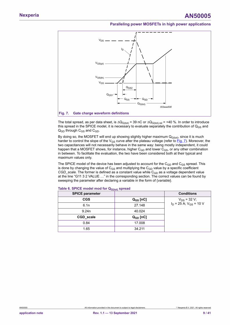
5.2.1. Total input charge – QG(tot)Table 5 gives the typical and maximum values for gate charge parameters QG(tot), QGS and QGD;refer to Fig. 7 for definitions of these parameters.
Table 5. BUK7S1R0-40H data sheet characteristics: gate chargeSymbol Parameter Conditions Min Typ Max UnitQG(tot) total gate charge - 98 137 nCQGS gate-source charge - 27 40 nCQGD gate-drain charge
ID = 25 A; VDS = 32 V; VGS = 10 V
- 17 34 nC
AN50005 All information provided in this document is subject to legal disclaimers. © Nexperia B.V. 2021. All rights reserved
application note Rev. 1.1 — 13 September 2021 8 / 41
Nexperia AN50005Paralleling power MOSFETs in high power applications
003aaa508
VGS
VGS(th)
QGS1
QGS2
QGD
VDS
QG(tot)
ID
QGS
VGS(pl)
Fig. 7. Gate charge waveform definitions
The total spread, as per data sheet, is ∆QG(tot) = 39 nC or ∆QG(tot),rel = +40 %. In order to introducethis spread in the SPICE model, it is necessary to evaluate separately the contribution of QGS andQGD through CGS and CGD.
By doing so, the MOSFET will end up showing slightly higher maximum QG(tot), since it is muchharder to control the slope of the VGS curve after the plateau voltage (refer to Fig. 7). Moreover, thetwo capacitances will not necessarily behave in the same way: being mostly independent, it couldhappen that a MOSFET shows, for instance, higher CGD and lower CGS, or any other combinationin between. To facilitate the evaluation, the two have been considered both at their typical andmaximum values only.
The SPICE model of the device has been adjusted to account for the CGD and CGS spread. Thisis done by changing the value of CGS and multiplying the CGD value by a specific coefficientCGD_scale. The former is defined as a constant value while CGD as a voltage dependent valueat the line “G11 3 2 VALUE …” in the corresponding section. The correct values can be found bysweeping the parameter after declaring a variable in the form of variable.
Table 6. SPICE model mod for QG(tot) spreadSPICE parameter Conditions
CGS QGS [nC]6.1n 27.148
9.24n 40.024CGD_scale QGD [nC]
0.84 17.0081.65 34.211
VDS = 32 V;ID = 25 A; VGS = 10 V
AN50005 All information provided in this document is subject to legal disclaimers. © Nexperia B.V. 2021. All rights reserved
application note Rev. 1.1 — 13 September 2021 9 / 41

Nexperia AN50005Paralleling power MOSFETs in high power applications
I(A)
D
30
-10
10
70
50
time (µs)0 10 20 30 40 50
aaa-033646
M2
M1
M3
Fig. 8. MOSFETs drain current (ID) - effects of QG(tot) spread
The simulation setup and results are summarized in Table 7. The value of QG(tot) has beencalculated as the sum of the respective QGS and QGD (from Table 6). At turn-ON the device withlower input capacitance (M1) will switch ON first thus handling majority of the current. On theother hand, at turn-OFF the MOSFET with higher input capacitance (M3) will switch OFF last nowhandling most of the current. The sharing during switching is the most impacted, while conductionhas changed only marginally. M3 is now dissipating 2.8 W (0.7 W more than the ideal case) whileM1 is dissipating 1.9 W.
Table 7. Summary - Effects of QG(tot) spreadDevice QG(tot) [nC] ESW(ON) [µJ] ESW(OFF)
[µJ]EnergySharing
Switching
ECOND [µJ] EnergySharing
ConductionM1 94.4 9.4 35.7 21.4 % 49.9 35.8 %M2 125.7 6.9 60.8 31.9 % 46.1 33.2 %M3 158.0 4.7 94.4 46.7 % 43.2 31.0 %
5.2.2. Gate-source threshold voltage – VGS(th)
Table 8. BUK7S1R0-40H data sheet characteristics: VGS(th)Symbol Parameter Conditions Min Typ Max Unit
ID = 1 mA; VDS=VGS; Tj = 25 °C 2.4 3 3.6 VID = 1 mA; VDS=VGS; Tj = 175 °C 1 - - V
VGS(th) gate-source thresholdvoltage
ID = 1 mA; VDS=VGS; Tj = -55 °C - - 4.3 V
The total spread, as per data sheet, is ∆VGS(th) = 1.2 V or ∆VGS(th),rel = ± 20 %. The SPICE modelof the device has been adjusted to account for the VGS(th) spread. This is done by changing thevalue of the Vto parameter located in the “.MODEL MINT NMOS” section. The correct values canbe found by sweeping the parameter after declaring a variable in the form of variable.
Table 9. SPICE model mod for VGS(th) spreadSPICE parameter Vto VGS(th) [V] Conditions
3.243 2.4003.843 3.0004.443 3.600
VDS = 12 V, ID = 1 mA
AN50005 All information provided in this document is subject to legal disclaimers. © Nexperia B.V. 2021. All rights reserved
application note Rev. 1.1 — 13 September 2021 10 / 41

Nexperia AN50005Paralleling power MOSFETs in high power applications
The MOSFETs drain current is shown in Fig. 9. After turn-ON, the loop inductance present in thecircuit causes the current to stabilise only after 10 µs, further details in the Layout-dependentparasitics section.
I(A)
D
30
-10
10
90
110
70
50
time (µs)0 10 20 30 40 50
aaa-033645
M1
M2
M3
Fig. 9. MOSFETs drain current (ID) - effects of VGS(th) spread
The simulation setup and results are summarized in Table 10. The MOSFET having lower VGS(th)will need to handle more energy overall. At turn-ON M1 will switch ON first thus handling majorityof the current. Moreover, at turn-OFF the same MOSFET will switch OFF last, again, handlingmost of the current. The sharing during switching is the most impacted, with one MOSFET (M3)participating only minimally in the process, while conduction has changed only marginally. M1 isnow dissipating 4.7 W (2.6 W more than the ideal case) while M3 only 1 W.
Table 10. Summary - Effects of VGS(th) spreadDevice VGS(th) [V] ESW(ON) [µJ] ESW(OFF)
[µJ]EnergySharing
Switching
ECOND [µJ] EnergySharing
ConductionM1 2.4 9.3 172.2 74.4 % 52.7 37.8 %M2 3 5.1 48.7 22.1 % 45.7 32.8 %M3 3.6 2.2 6.4 3.5 % 40.8 29.4 %
In conclusion, the MOSFET having lower VGS(th) will need to handle more energy both duringturn-ON and turn-OFF, while with the capacitance spread the switching energy will be balancedbetween at least two devices. These results are valid only for the first cycles of operation, dueto the temperature dependency of the VGS(th). More information is provided in the correspondingsection on temperature dependency. Refer to Section 7.1 for an explanation of the shape of thecurrent between switching and conduction, as shown in Fig. 6, Fig. 8 and Fig. 9.
AN50005 All information provided in this document is subject to legal disclaimers. © Nexperia B.V. 2021. All rights reserved
application note Rev. 1.1 — 13 September 2021 11 / 41

Nexperia AN50005Paralleling power MOSFETs in high power applications
5.3. Paralleled MOSFETs and temperature dependencyEach MOSFET can be thought as a system composed of an electrical subsystem in a feedbackloop with a thermal subsystem, as shown in Fig. 10.
aaa-033729
ELECTRICALSUB-SYSTEM
THERMALSUB-SYSTEM
Fig. 10. MOSFET electrical-thermal interaction
Power MOSFETs are often considered to be immune to thermal runaway due to the RDSontemperature coefficient. However, this is only true for MOSFETs that are fully ON. When aMOSFET is in the on-state, there are two competing effects that determine how its current behaveswith increasing temperature. As the temperature rises, VGS(th) falls, thereby increasing the current.On the other hand, RDSon increases with increasing temperature, thereby reducing the current. Theresistance increase dominates at higher gate-source voltages (VGS), while the threshold-voltagedrop dominates at low VGS. Consequently, for a given VDS, there is a critical VGS below which thereis a positive feedback regime and above which there is a negative feedback and thermal stability.This critical point is known as the Zero Temperature Coefficient (ZTC) point, Fig. 11.
aaa-032641
0 1 2 3 4 5 6 7 80
70
140
210
280
350
VGS (V)
ID(A)
Tj = -55°CTj = -55°C25°C25°C
175°C175°C
ZTC
Fig. 11. BUK7S2R5-40H data sheet graph: transfer characteristic ZTC point
The interaction between thermal and electrical subsystems can be simulated using Nexperiaadvanced models1 which make two additional thermal pins accessible: junction and case/mountingbase. Within these models, parameters of interest for the paralleling are modelled with increasedaccuracy by including their temperature dependency. A circuit modelling the overall thermal systemMOSFET-PCB-ambient to the drain tab must be connected to the mounting base pin of the model.
1 The advanced models will be released later in 2021
AN50005 All information provided in this document is subject to legal disclaimers. © Nexperia B.V. 2021. All rights reserved
application note Rev. 1.1 — 13 September 2021 12 / 41

Nexperia AN50005Paralleling power MOSFETs in high power applications
5.3.1. Temperature dependency during static operation (DC)In a parallel configuration, RDSon has the advantage of improving the sharing due to its positivetemperature coefficient (PTC), Fig. 12. As one MOSFET conducts more current and dissipatesmore power, RDSon increases and the conduction losses change improving the sharing.
aaa-026897
-60 -30 0 30 60 90 120 150 1800
0.4
0.8
1.2
1.6
2
2.4
Tj (°C)
aa
a RDSon(25°C)= DSonR
Fig. 12. BUK7S2R5-40H data sheet graph: normalized on-state resistance as a function ofjunction temperature
Ideally this phenomenon is maximized when the thermal coupling between paralleled MOSFETs isless effective, as each MOSFET is less influenced by the others around it. However, this leads tohigher junction temperatures. This phenomenon can be described using the steady state simulationshown in Fig. 13. This time, to simplify the interaction, only two MOSFETs have been used inparallel. Additionally, a second circuit is used to model the thermal coupling between the twoMOSFETs and their connection with the PCB.
The SPICE model of the devices have been adjusted in order for M1 to show lower RDSon(0.62 mΩ) than M2 (1 mΩ).
aaa-033635
Rg1Tj1
TjM1
Rg2
3.9
Rth(M1-M2)
Rgdrv
12
3.9
Vgs
15 VVsupply
12 V
Tc1TcaseBUK7S1R0-40H_RDSonMIN
Tj2
Tc1
TjM2
Tc2TcaseBUK7S1R0-40H_RDSonMAX
Rload119.3 m
Rpcb_M140
Tc2
Rpcb_M240
Tamb
25 V
Fig. 13. SPICE simulation circuit: thermal coupling
AN50005 All information provided in this document is subject to legal disclaimers. © Nexperia B.V. 2021. All rights reserved
application note Rev. 1.1 — 13 September 2021 13 / 41

Nexperia AN50005Paralleling power MOSFETs in high power applications
With reference to the graph in Fig. 14: the total current flowing through the devices is set at 100 Aso that the leftmost y-axis shows current and sharing in percentage at the same time. In this casecurrent has been used to calculate the degree of sharing between the MOSFETs as this exampleconsiders purely steady state conduction. As the thermal coupling between the two MOSFETsworsens (Rth(M1-M2) increases) the junction temperature of M1 increases while the currentsharing in steady state improves (converges more towards 50 %). Moreover, even in case of highdecoupling the RDSon PTC will only improve the sharing by a maximum of around 2 % for eachMOSFET.
Therefore good thermal coupling between paralleled MOSFETs is to be preferred as it allows forlower junction temperatures. More details on this are provided in the PCB Layout influence: Circuitlayout section.
180
100
120
140
160
200Tj (°C)
Currentsharing
(%)
aaa-033648
80
0
20
40
60
100
0.1 1 10 100 1,000R th(M1-M2) (K/W)
M1 current share M2 current sharej M2 TM1 T j
ID(A)
Fig. 14. Thermal coupling influence on sharing: RDSon(M1) = 0.62 mΩ andRDSon(M2) = 1 mΩ
5.3.2. Temperature dependency during dynamic operationThreshold voltage is characterized by a negative temperature coefficient (NTC): it decreases as thejunction temperature increases. This behaviour is more detrimental in case of paralleled MOSFETs.For instance, a device with an initial higher junction temperature will exhibit an even lower VGS(th)which increases the current flowing through the MOSFET and thus the power that it dissipates.As in the static case, good thermal coupling helps to keep the MOSFETs at similar temperatures.Other guidelines could be adopted to mitigate temperature gradient across paralleled MOSFETs,for more information refer to PCB Layout influence: Circuit layout.
Fig. 15 shows how the VGS(th) spread is almost constant with respect to the junction temperature,however this behaviour is guaranteed only at a drain current of 1 mA. For a temperature differenceof 20 °C (from 25 to 45 °C) VGSth reduces by about 0.2 V.
AN50005 All information provided in this document is subject to legal disclaimers. © Nexperia B.V. 2021. All rights reserved
application note Rev. 1.1 — 13 September 2021 14 / 41

Nexperia AN50005Paralleling power MOSFETs in high power applications
aaa-018139
-60 -30 0 30 60 90 120 150 1800
1
2
3
4
5
Tj (°C)
VGS(th)VGS(th)(V)(V)
TypTyp
MinMin
MaxMax
Fig. 15. BUK7S1R0-40H data sheet graph: gate-source threshold voltage as a function ofjunction temperature
Finally, unlike RDSon and VGS(th), input charge is shown to only slightly vary with temperature.
5.4. Data sheet and batch spreadsIf considering multiple MOSFETs in parallel, data sheet spreads may be too conservative. Thedesign would certainly be reliable but the improved robustness to a wider worst case scenariocould end up being more expensive. In this case then, the designer would prefer to evaluate aless stringent worst case scenario that, even if not guaranteed like the data sheet, can still beconsidered realistic. This is done by looking at batch spreads.
A batch refers to a group of devices that go through the whole manufacturing process at thesame time. The number of dies in a batch can vary from a few thousands to over a few millions,depending on the size of the dies themselves. Within a set of paralleled MOSFETs, it is preferableto choose parts coming from the same reel in order to increase the possibility of using devices fromthe same batch. Furthermore, using MOSFETs with identical batch codes, which can be found onthe package under the marking code, could be used to further narrow down the selection duringPCB assembly.
Spreads within a batch are observed to be much lower than the corresponding data sheet ones.The same can be said even with those among different batches. Fig. 16 shows the spread ofVGS(th) for the BUK7S1R5-40H for 10 different batches. In this case the 6-sigma spread is observedto be 0.42 V, from 2.86 V to 3.28 V. This value is calculated taking into account a small quantity ofoutliers (not shown in the plot of Fig. 16). Therefore, the observed worst case is given by a ΔVGS(th)= 0.42 V or ΔVGS(th),rel = ± 7 %, less than half of the guaranteed (data sheet) one.
AN50005 All information provided in this document is subject to legal disclaimers. © Nexperia B.V. 2021. All rights reserved
application note Rev. 1.1 — 13 September 2021 15 / 41

Nexperia AN50005Paralleling power MOSFETs in high power applications
aaa-033732
(V)VGS(th)
3.6
2.1
3.1
2.6
Batch
4.6
1.6
4.1
2 43 5 6 7 8 9 10
Data sheet max
Data sheet min
1
Fig. 16. VGS(th) batches spread for BUK7S1R5-40H
Fig. 17 shows the absolute value of the difference in VGS(th) (|∆VGS(th)|) between two consecutivedevices, within two different batches. In this case the 6-sigma spread is observed to be 0.25 V,or ΔVGS(th),rel = ±4 %. Therefore, in case two consecutive MOSFETs coming from the same reelare used in parallel, the difference between their VGS(th) is observed to be even smaller than thatbetween multiple batches.
0.3
0.2
0.1
0
|∆VGS(th)|
aaa-033949
(V)
Fig. 17. Absolute value of the difference in VGS(th) between two consecutive devices
Fig. 18 compares the MOSFETs drain current in case of data sheet and batch spread, Table 11quotes the energy shared by each MOSFET. M1 is now dissipating a total of 2.8 W and M3 1.5 W.Therefore, a difference of ±7 % in VGS(th) leads to a reduction of 1.9 W over a cycle of M1, reducingthe ratio between these two MOSFETs dissipation from almost 5:1 down to 2.5:1.
AN50005 All information provided in this document is subject to legal disclaimers. © Nexperia B.V. 2021. All rights reserved
application note Rev. 1.1 — 13 September 2021 16 / 41

Nexperia AN50005Paralleling power MOSFETs in high power applications
I(A)
D
30
-10
10
90
110
70
50
time (µs)0 10 20 30 40 50
aaa-033645
M1
M2
M3
a. data sheet spread
I(A)
D
30
-10
10
90
70
50
time (µs)0 10 20 30 40 50
aaa-033647
M1
M3M2
b. batch spread
Fig. 18. MOSFETs drain current (ID) – data sheet and batch VGS(th) spread comparison
Table 11. Summary - Effects of VGS(th) batch spreadDevice VGS(th) [V] ESW [µJ] Energy
SharingSwitching
ECOND [µJ] EnergySharing
ConductionM1 2.79 97.0 51.3 % 48.7 35.6 %M2 3 59.4 31.4 % 45.4 33.2 %M3 3.21 32.6 17.2 % 42.7 31.2 %
6. Circuit optimisationThere are two main types of circuit modifications, each has a different impact on the currentsharing. These are: localized gate resistor and components in the MOSFETs source paths.
6.1. Localized gate resistorThe first type of circuit modification is also the most advantageous, it has no major drawbacksand it is the simplest to implement. The modification involves splitting the gate resistor betweena localized one close to the gate of each MOSFET and a common resistor at the driver side, asshown in Fig. 18 b. Doing so will counteract the spreads and improve the sharing, mainly duringswitching with little impact during conduction.
It is important to keep the localized resistance as low as possible to give maximum couplingbetween the MOSFET gates, effectively allowing the input capacitances to be considered inparallel. A simple simulation can display this effect: two circuits modelling the driver and inputimpedance of each MOSFET are used as comparison. Fig. 19 a. shows the control voltage at eachMOSFET gate, the voltage is slowed down in case of the MOSFET with higher Ciss, vice versa it isless filtered in case of lower capacitance.
By splitting the gate resistor the difference between the control voltages at each gate becomesnegligible (Fig. 19 b). With reference to the naming adopted in the SPICE circuits of Fig. 19, thegate resistor at the driver can be calculated as:
=RG,drv -RnFETR
nFETG G,split (5)
The value of RG,drv has been rounded to 12 Ω. A smaller RG,drv can be beneficial by reducingthe switching time where the unequal sharing occurs. In a similar manner, the smaller RG,split thebetter coupled the MOSFETs gate, but it is recommended not to go below 2-3 Ω. In general, a gateresistor helps in dampening any oscillation in the gate-source loop that might compromise the EMCperformance of the system. Therefore, given a lower resistance of the gate resistor, it is importantto reduce as much as possible the loop inductance of the driver loop, for further information seesection: PCB layout influence.
AN50005 All information provided in this document is subject to legal disclaimers. © Nexperia B.V. 2021. All rights reserved
application note Rev. 1.1 — 13 September 2021 17 / 41

Nexperia AN50005Paralleling power MOSFETs in high power applications
aaa-033636
Vg1
RG139 Ω
Ciss11 nF
gate1
RG239 Ω
Ciss22 nF
gate2
RG339 Ω
Ciss33 nF
gate3
PULSE (0 15 0 1nF 1nF 1)
Vg2
RGsplit13.9 Ω
Rgdrv
12 Ω
Ciss11 nF
gate1
RGsplit23.9 Ω
Ciss22 nF
gate2
RGsplit33.9 Ω
Ciss33 nF
gate3
PULSE (0 15 0 1nF 1nF 1)
a. without gate resistor split b. with gate resistor split
Fig. 19. SPICE simulation circuit: gate resistor split comparison
time (µs)0 10 20 30 40 50
V
(V)GS
4
16
8
12
0
aaa-033649
M1
M2
M3
a. without gate resistor splittime (µs)0 10 20 30 40 50
V
(V)GS
4
16
8
12
0
aaa-033650
M1
M3
M2
b. with gate resistor split
Fig. 20. Gate-source voltage without and with gate resistor split
The great improvement of the resistor split can be easily appreciated by simulating the same half-bridge circuit using two different gate resistors setups and introducing some spread. This time anarbitrary combination of all the spreads has been used. Fig. 21 shows the MOSFETs drain currentwithout gate resistor split, while Fig. 22 shows the MOSFETs drain current with gate resistor split.
aaa-033651
time (µs)0 10 20 30 40 50-20
I(A)
D
40
160
80
120
0
20
60
100
140
M1
M3
M2
Fig. 21. MOSFETs drain current (ID) – without gate resistor split
The simulations setup and results are summarized in Table 12 and Table 13, while a finalcomparison is given in Table 14. M3 is dissipating 8.2 W, M2 1.3 W and M1 2.0 W. At turn-ONM1 is switching first, due to having both lower QG(tot) and VGS(th), thus handling the majority of thecurrent. On the other hand, at turn-OFF the MOSFET with higher input charge (M3) will switch lastand carry most of the current.
AN50005 All information provided in this document is subject to legal disclaimers. © Nexperia B.V. 2021. All rights reserved
application note Rev. 1.1 — 13 September 2021 18 / 41
Nexperia AN50005Paralleling power MOSFETs in high power applications
Table 12. Summary - sharing without gate resistor split: RG = 39 ΩDevice RDSon
[mΩ]VGS(th) [V] QG(tot)
[nC]ESW [µJ] Energy
SharingSwitching
ECOND [µJ] EnergySharing
ConductionM1 0.62 3.21 94.4 42.7 9.6 % 62.2 47.0 %M2 1 3 125.7 29.0 6.5 % 35.2 26.6 %M3 0.88 2.79 158.0 373.0 83.9 % 34.9 26.4 %
aaa-033652
time (µs)0 10 20 30 40 50-20
I(A)
D
40
80
0
20
60
100
M1
M3
M2
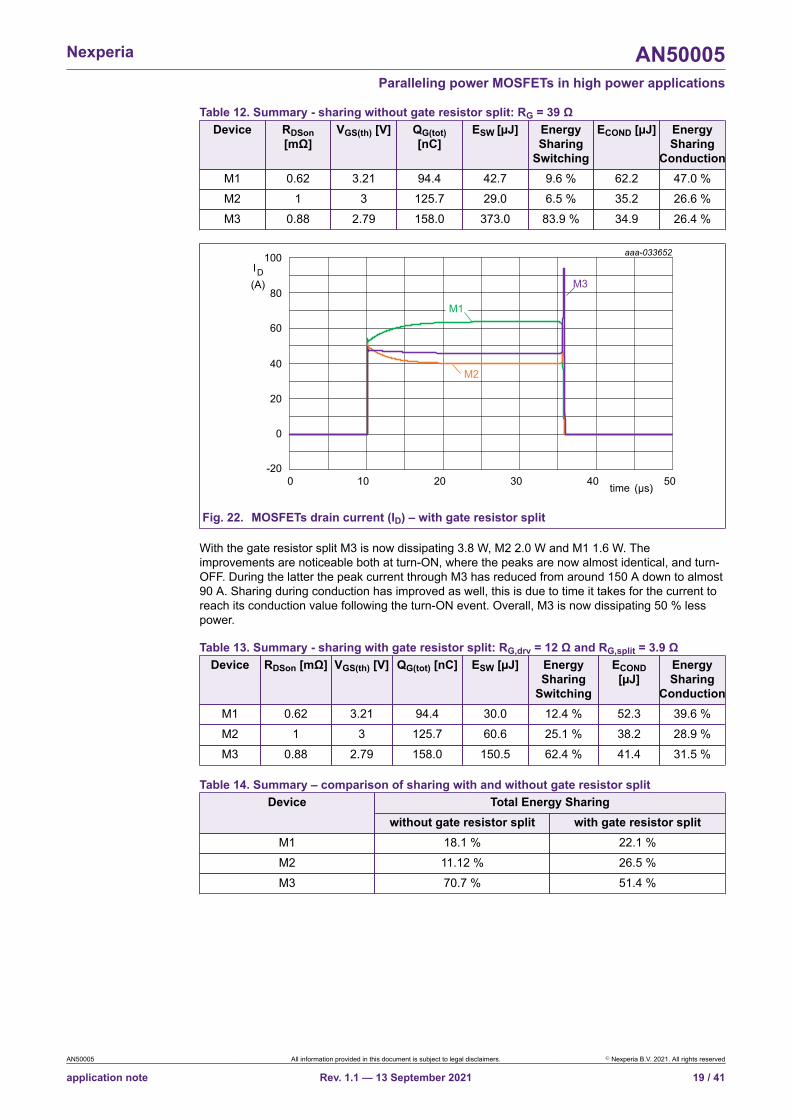
Fig. 22. MOSFETs drain current (ID) – with gate resistor split
With the gate resistor split M3 is now dissipating 3.8 W, M2 2.0 W and M1 1.6 W. Theimprovements are noticeable both at turn-ON, where the peaks are now almost identical, and turn-OFF. During the latter the peak current through M3 has reduced from around 150 A down to almost90 A. Sharing during conduction has improved as well, this is due to time it takes for the current toreach its conduction value following the turn-ON event. Overall, M3 is now dissipating 50 % lesspower.
Table 13. Summary - sharing with gate resistor split: RG,drv = 12 Ω and RG,split = 3.9 ΩDevice RDSon [mΩ] VGS(th) [V] QG(tot) [nC] ESW [µJ] Energy
SharingSwitching
ECOND[µJ]
EnergySharing
ConductionM1 0.62 3.21 94.4 30.0 12.4 % 52.3 39.6 %M2 1 3 125.7 60.6 25.1 % 38.2 28.9 %M3 0.88 2.79 158.0 150.5 62.4 % 41.4 31.5 %
Table 14. Summary – comparison of sharing with and without gate resistor splitTotal Energy SharingDevice
without gate resistor split with gate resistor splitM1 18.1 % 22.1 %M2 11.12 % 26.5 %M3 70.7 % 51.4 %
AN50005 All information provided in this document is subject to legal disclaimers. © Nexperia B.V. 2021. All rights reserved
application note Rev. 1.1 — 13 September 2021 19 / 41
Nexperia AN50005Paralleling power MOSFETs in high power applications
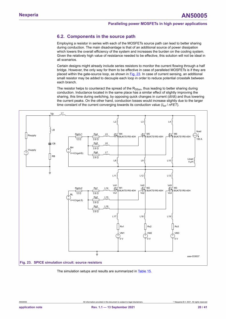
6.2. Components in the source pathEmploying a resistor in series with each of the MOSFETs source path can lead to better sharingduring conduction. The main disadvantage is that of an additional source of power dissipationwhich lowers the overall efficiency of the system and increases the burden on the cooling system.Given the relatively high value of resistance needed to be effective, this solution will not be ideal inall scenarios.
Certain designs might already include series resistors to monitor the current flowing through a halfbridge. However, the only way for them to be effective in case of paralleled MOSFETs is if they areplaced within the gate-source loop, as shown in Fig. 23. In case of current sensing, an additionalsmall resistor may be added to decouple each loop in order to reduce potential crosstalk betweeneach branch.
The resistor helps to counteract the spread of the RDSon, thus leading to better sharing duringconduction. Inductance located in the same place has a similar effect of slightly improving thesharing, this time during switching, by opposing quick changes in current (dI/dt) and thus loweringthe current peaks. On the other hand, conduction losses would increase slightly due to the largertime constant of the current converging towards its conduction value (Itot / nFET).
aaa-033637
Rsupply
Vsupply
LB
L1Vp
RB
CB
BL
V=V(VgsLS)
VM1
0 V
Rgdrv2
12 Ω
Rg1 M1BUK7S1R0-40H
L14Vd1
Vs13.9 Ω
Rg2 L15
3.9 Ω
Rg3 L16
L17
Rx1 Rx2 Rx3
VM2
0 V
M2BUK7S1R0-40H
Vd2
Vs2
L18
VM3
0 V
M3BUK7S1R0-40H
Vd3
Vs3
L19
L11 L12 L13
L8 L9 L10
3.9 Ω
BH
V=V(VgsHS)
Iload
150 A
Rgdrv1
12 Ω
Rg4 M4BUK7S1R0-40H
L5
3.9 Ω
Rg5 L6
3.9 Ω
Rg6 L7
Lload4 µH
M5BUK7S1R0-40H
M6BUK7S1R0-40H
L2 L3 L4
3.9 Ω
Fig. 23. SPICE simulation circuit: source resistors
The simulation setups and results are summarized in Table 15.
AN50005 All information provided in this document is subject to legal disclaimers. © Nexperia B.V. 2021. All rights reserved
application note Rev. 1.1 — 13 September 2021 20 / 41

Nexperia AN50005Paralleling power MOSFETs in high power applications
I(A)
D
20
-20
0
80
100
60
40
time (µs)0 10 20 30 40 50
aaa-033653
M1
M2
M3
Fig. 24. MOSFETs drain current (ID) – with a source resistor of 1 mΩ
Table 15. Summary – sharing with a source resistor of 1 mΩDevice RDSon
[mΩ]VGS(th) [V] QG(tot)
[nC]ESW [µJ] Energy
SharingSwitching
ECOND [µJ EnergySharing
ConductionM1 0.62 3.21 94.4 27.9 11.5 % 41.6 30.8 %M2 1 3 125.7 66.5 27.4 % 47.3 35.1 %M3 0.88 2.79 158.0 148.4 61.1 % 46.1 34.1 %
The efficacy of the resistor on the current sharing depends on its value. If the aim is to balancethe current sharing, then the higher the resistance the better, as shown in Fig. 25. Naturally thedissipation will increase considerably with it. In order for it to be effective in counteracting the RDSonspread it needs to be comparable with the actual RDSon of the MOSFET.
I(A)
D
10
-10
50
70
30
time (µs)0 10 20 30 40 50
aaa-033654
RS = 1 µΩRSR SRS
= 250 mΩ= 500 µΩ= 1 mΩ
Fig. 25. MOSFETs drain current (ID) – effects of source resistor value
AN50005 All information provided in this document is subject to legal disclaimers. © Nexperia B.V. 2021. All rights reserved
application note Rev. 1.1 — 13 September 2021 21 / 41
Nexperia AN50005Paralleling power MOSFETs in high power applications
7. PCB layout influenceTight spreads and a good layout are two important factors when designing an application withparalleled MOSFETs. This chapter describes guidelines to achieve a good layout and howparasitics influence the current sharing.
In a paralleled set of MOSFETs it is impossible to say beforehand where the device with lowest orhighest spreads will be placed. Therefore, it is important to lay out each branch in the same way,failing to do so will result in the worsening of the worst case scenario.
7.1. Layout-dependent parasiticsIn case of paralleled devices loop inductance and resistance in the path should be not onlyminimised but also equalised for each branch.
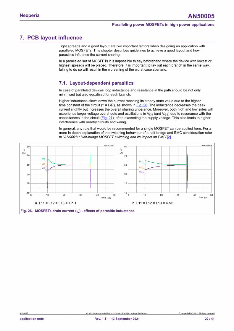
Higher inductance slows down the current reaching its steady state value due to the highertime constant of the circuit (τ = L/R), as shown in Fig. 26. The inductance decreases the peakcurrent slightly but increases the overall sharing unbalance. Moreover, both high and low sides willexperience larger voltage overshoots and oscillations in VDS (and VGS) due to resonance with thecapacitances in the circuit (Fig. 27), often exceeding the supply voltage. This also leads to higherinterference with nearby circuits and wiring.
In general, any rule that would be recommended for a single MOSFET can be applied here. For amore in depth explanation of the switching behaviour of a half-bridge and EMC consideration referto “AN90011: Half-bridge MOSFET switching and its impact on EMC”[2]
I(A)
D
30
-10
10
90
70
50
time (µs)0 10 20 30 40 50
aaa-033647
M1
M3M2
a. L11 = L12 = L13 = 1 nH
I(A)
D
30
-10
10
90
70
50
time (µs)0 10 20 30 40 50
aaa-033659
M1
M3
M2
b. L11 = L12 = L13 = 4 nH
Fig. 26. MOSFETs drain current (ID) - effects of parasitic inductance
AN50005 All information provided in this document is subject to legal disclaimers. © Nexperia B.V. 2021. All rights reserved
application note Rev. 1.1 — 13 September 2021 22 / 41
Nexperia AN50005Paralleling power MOSFETs in high power applications
V(V)
DS
4
-4
28
12
time (µs)35.0 35.2 35.4 35.6 35.8 37.0
aaa-033660
20
L = 4 nHp_DL = 1 nHp_D
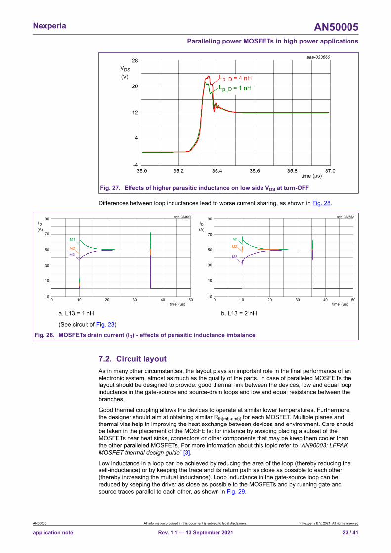
Fig. 27. Effects of higher parasitic inductance on low side VDS at turn-OFF
Differences between loop inductances lead to worse current sharing, as shown in Fig. 28.
I(A)
D
30
-10
10
90
70
50
time (µs)0 10 20 30 40 50
aaa-033647
M1
M3M2
a. L13 = 1 nH
I(A)
D
30
-10
10
90
70
50
time (µs)0 10 20 30 40 50
aaa-033662
M1
M3
M2
b. L13 = 2 nH
(See circuit of Fig. 23)
Fig. 28. MOSFETs drain current (ID) - effects of parasitic inductance imbalance
7.2. Circuit layoutAs in many other circumstances, the layout plays an important role in the final performance of anelectronic system, almost as much as the quality of the parts. In case of paralleled MOSFETs thelayout should be designed to provide: good thermal link between the devices, low and equal loopinductance in the gate-source and source-drain loops and low and equal resistance between thebranches.
Good thermal coupling allows the devices to operate at similar lower temperatures. Furthermore,the designer should aim at obtaining similar Rth(mb-amb) for each MOSFET. Multiple planes andthermal vias help in improving the heat exchange between devices and environment. Care shouldbe taken in the placement of the MOSFETs: for instance by avoiding placing a subset of theMOSFETs near heat sinks, connectors or other components that may be keep them cooler thanthe other paralleled MOSFETs. For more information about this topic refer to “AN90003: LFPAKMOSFET thermal design guide” [3].
Low inductance in a loop can be achieved by reducing the area of the loop (thereby reducing theself-inductance) or by keeping the trace and its return path as close as possible to each other(thereby increasing the mutual inductance). Loop inductance in the gate-source loop can bereduced by keeping the driver as close as possible to the MOSFETs and by running gate andsource traces parallel to each other, as shown in Fig. 29.
AN50005 All information provided in this document is subject to legal disclaimers. © Nexperia B.V. 2021. All rights reserved
application note Rev. 1.1 — 13 September 2021 23 / 41

Nexperia AN50005Paralleling power MOSFETs in high power applications
aaa-033641
+ve supply
switch node
Fig. 29. Gate-source loop: possible layout
Inductance in the loop carrying the load current could be minimised, for instance, by employingthe design in Fig. 30. For further details refer to “AN90011: Half-bridge MOSFET switching and itsimpact on EMC” [2].
aaa-031121
4 mm
2.07 nH
4.75 nH
VDC
D1
S2
I/P
3.5 nH
3.5 nH
2.07 nH
4.75 nH
C
+ve supplyground plane
(on another PCB layer)
switch node
aaa-031122
VDCC
D1
S2
I/P 4.04 nH
1.55 nH
2.52 nH
4.04 nH
1.55 nH
2.52 nH2.52 nH
switch node
ground plane(on another PCB layer)
+ve supply
Fig. 30. Half-bridge layout possibilities showing inductances
The placement of inlets and outlets plays another important role because it determines eachbranch parasitics. When using multiple devices in parallel, it could be helpful to use more than oneinlet and outlet. Using multiple smaller cables can be actually beneficial for other reasons too. Thepositioning of these insertion points needs to be carefully planned. One possible way to facilitate
AN50005 All information provided in this document is subject to legal disclaimers. © Nexperia B.V. 2021. All rights reserved
application note Rev. 1.1 — 13 September 2021 24 / 41

Nexperia AN50005Paralleling power MOSFETs in high power applications
this decision might be to use a CFD software and run a current density simulation. This type ofsimulation highlights the preferred path the current takes in a steady state condition (DC).
Fig. 31 shows the setup used for the simulations: 3 MOSFETs are placed in parallel both at highand low side. Each low side MOSFET is connected between phase (inlet), on the top layer, andground (outlet) on the bottom one (not shown in the picture), through a number of filled vias. Eachhigh side is instead connected between phase (outlet) and the positive supply (inlet) on the toplayer. A total current of 150 A is set to flow through the paralleled devices. Two simulations arerequired, each with a single side active at a time.
aaa-033743
Fig. 31. CFD simulation setup
The results of the current density simulation for the low side and high side are shown in Fig. 32,Fig. 33 and Fig. 34. Higher current density is shown in red, while low or null in blue. For instancethe high side simulation (Fig. 34) highlights a spot around M4 and inlet VBUS1 where currentdensity is higher, due to the position of the latter. By integrating the current density over the entiresurface of the die it is possible to calculate the sharing in steady state of the layout (between30-40% in this particular case). These simulations have been obtained using scSTREAM.
AN50005 All information provided in this document is subject to legal disclaimers. © Nexperia B.V. 2021. All rights reserved
application note Rev. 1.1 — 13 September 2021 25 / 41

Nexperia AN50005Paralleling power MOSFETs in high power applications
aaa-033747
Fig. 32. CFD current density simulation: Low side MOSFETs ON – Top side
aaa-033748
Fig. 33. CFD current density simulation: Low side MOSFETs ON – Bottom side
AN50005 All information provided in this document is subject to legal disclaimers. © Nexperia B.V. 2021. All rights reserved
application note Rev. 1.1 — 13 September 2021 26 / 41

Nexperia AN50005Paralleling power MOSFETs in high power applications
aaa-033749
Fig. 34. CFD current density simulation: High side MOSFETs ON – Top side
8. Driving paralleled MOSFETsWhen driving paralleled MOSFETs it is recommended to use one single gate driver. This is mainlydone to synchronize the devices operation as much as possible.
The gate driver should have enough peak current capability to fully charge and discharge the totalinput capacitance of the paralleled MOSFETs. This requirement becomes more and more stringentas the number of MOSFETs increases, especially if the switching time is required to be low, as thetotal input capacitance is now Ciss,tot = n.FETs × Ciss,max. Failing to do so means that the switchingspeed will be set by the gate driver itself and not by the gate resistor.
As shown by the previous simulations turn-OFF dissipates more energy than turn-ON. One simpleway to reduce the switching losses is by decreasing the resistance of RG,drv only during the turn-OFF. This can be done by using a combination of a smaller resistor in series with a diode, placedin parallel with RG,drv, as shown in Fig. 35. However, before choosing the right value of RG,OFF itis recommended to take into account any parasitic inductance that may be present in the circuit: acombination of fast turn-OFF and high inductance could potentially induce avalanche, which, in aparallel configuration, could greatly stress the device with lower breakdown voltage.
aaa-033642
Rg_OFF
Rgdrv
D1
Fig. 35. Speeding up turn-OFF switching
AN50005 All information provided in this document is subject to legal disclaimers. © Nexperia B.V. 2021. All rights reserved
application note Rev. 1.1 — 13 September 2021 27 / 41

Nexperia AN50005Paralleling power MOSFETs in high power applications
9. Simulation toolsThis chapter describes how to set up a simulation aimed at finding the worst case scenario in aset of paralleled MOSFETs. In this case SPICE has been used, however, the same ideas can beapplied to any other simulation tool that offers the same functionality.
The idea is to take into account MOSFET spreads in a simulation, in the same way of usualcomponents tolerances. Two types of simulations are discussed: probability distribution and worstcase scenario simulations.
Probability distribution simulation refers to a simulation where one or more parameters are definedby their probability distribution, generally shown to be approximately Gaussian (or Normal).This type of simulation would have the advantage of weighting each possible combination bythe likelihood of it happening. In theory, this would yield a more realistic evaluation and thedesigner could run the simulation for a number of iterations corresponding to the design BOM(bill of materials). In practice this type of evaluation is impractical since the data correspondingto parameters distribution (mainly sigma value) would need to be measured for each specificpart name, it would not be guaranteed and it would require additional expensive steps in themanufacturing process.
With respect to a distribution based simulation, the worst case scenario reduces the number ofiterations by taking into account only the maximum distribution of a parameter around its typicalvalue. The amount of runs is reduced to 2N + 1, where N is the number of indexed parameters and1 is the nominal case, which is computed at the end. This type of evaluation is based on data sheetspreads, which are guaranteed. On the other hand, it might miss “local extrema”, i.e. points insidethe spread at which the outcome is worse than the one resulting from considering only maximum,minimum and nominal.
The analysis requires four main figures:
• Spreads, namely typical value and ∆ (tolerance)• A function binary(run, index) that creates a set of indexes for the various combinations• A function wc(nominal, tol, index) that reads these indexes and outputs the correct value for the
parameter• A function that automatically measures the average dissipated power over a cycle
Besides, the spreads need to be symmetrical so, in case of RDSon, the evaluation will either use ahigher minimum or maximum resistance than the data sheet one. Instead, in case the data sheetdoes not provide a minimum value, as for QG(tot), then the middle point can be considered asnominal.
Prior to running the simulation the spice model of each MOSFET needs to be modified to replacethe value of each parameter considered in the evaluation, with the output of the wc(nom, tol, index)function, as shown below:
• RDSon typical value 0.88 mΩ, tolerance ±0.12 mΩRD 3 4 wc(576.2603u,tol_RD,3) TC= 9.735m, 2.369u
• QGS typical value 33.5 nC, tolerance ± 13 nCCGS 2 6 wc(7.67n,tol_CGS,6)
• QGD typical value 25.5 nC, tolerance ± 17 nC.params CGD_scale = wc(1.245,tol_CGD,9)…G11 3 2 VALUE CGD_scale*V(13,0)*I(V11)
• VGS(th) typical value 3 V, tolerance ±0.21 VVto= wc(3.843,tol_VGSth,0)
where: tol_RD = 119.68u, tolCGS = 1.57n, tol_CGD = 0.405 and tol_VGSth = 0.21.
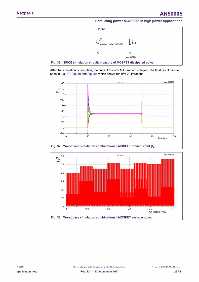
In this particular case the number of parameters are 4, these change between the 3 paralleledMOSFETs so the total number of indexed parameters is 12. Consequently the amount ofcombinations will be 212 + 1 = 4097. Only one MOSFET can be considered for this evaluation. Aslightly modified version of the circuit seen in Fig. 1 is used for this simulation. Furthermore, thesmall circuit of Fig. 36 is required in order to automatically compute the power dissipated by theMOSFET under investigation (the corresponding 0 V monitor generator is required too).
AN50005 All information provided in this document is subject to legal disclaimers. © Nexperia B.V. 2021. All rights reserved
application note Rev. 1.1 — 13 September 2021 28 / 41
Nexperia AN50005Paralleling power MOSFETs in high power applications
aaa-033639
B1
P_diss
V=(V(Vd1)-V(Vs1))*I(VM1)
R11 kΩ
Fig. 36. SPICE simulation circuit: measure of MOSFET dissipated power
After the simulation is complete, the current through M1 can be displayed. The final result can beseen in Fig. 37, Fig. 38 and Fig. 39, which shows the first 20 iterations.
aaa-033663
I(A)
D
160
-20
20
60
100
120
0
40
80
140
time (µs)0 5040302010
Fig. 37. Worst case simulation combinations - MOSFET drain current (ID)
4.5
0.9
1.5
2.7
2.1
3.3
3.9(W)
PAV
0 1.60.8 2.4 3.2 4run index (x1000)
aaa-033664
Fig. 38. Worst case simulation combinations - MOSFET average power
AN50005 All information provided in this document is subject to legal disclaimers. © Nexperia B.V. 2021. All rights reserved
application note Rev. 1.1 — 13 September 2021 29 / 41
Nexperia AN50005Paralleling power MOSFETs in high power applications
run index0 20168 12
aaa-033746
2
1
3
4P
04
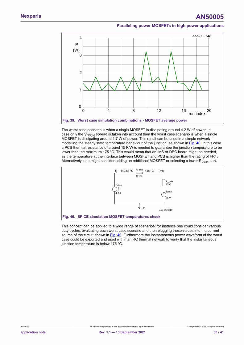
(W)
Fig. 39. Worst case simulation combinations - MOSFET average power
The worst case scenario is when a single MOSFET is dissipating around 4.2 W of power. Incase only the VGS(th) spread is taken into account then the worst case scenario is when a singleMOSFET is dissipating around 1.7 W of power. This result can be used in a simple networkmodelling the steady state temperature behaviour of the junction, as shown in Fig. 40. In this casea PCB thermal resistance of around 15 K/W is needed to guarantee the junction temperature to belower than the maximum 175 °C. This would mean that an IMS or DBC board might be needed,as the temperature at the interface between MOSFET and PCB is higher than the rating of FR4.Alternatively, one might consider adding an additional MOSFET or selecting a lower RDSon part.
aaa-033640
Tamb
85 V
Rj_mbTj 149.68 °C
R_pcb15
0.4
Pdiss
.op
4.2 A
Tmb148 °C
Fig. 40. SPICE simulation MOSFET temperatures check
This concept can be applied to a wide range of scenarios: for instance one could consider variousduty cycles, evaluating each worst case scenario and then plugging these values into the currentsource of the circuit shown in Fig. 40. Furthermore the instantaneous power waveform of the worstcase could be exported and used within an RC thermal network to verify that the instantaneousjunction temperature is below 175 °C.
AN50005 All information provided in this document is subject to legal disclaimers. © Nexperia B.V. 2021. All rights reserved
application note Rev. 1.1 — 13 September 2021 30 / 41

Nexperia AN50005Paralleling power MOSFETs in high power applications
10. ConclusionThis application note aims at giving the reader a description of how the sharing among paralleledMOSFETs is influenced by parameters spreads (e.g. RDSon, VGS(th) and QG(tot)) and PCB layout.The analysis is conducted considering switch-mode (PWM) applications and thus the half-bridgetopology.
During switching, VGS(th) spread contributes the most to current unbalances, affecting turn-ONand turn-OFF in the same way: the device with lower VGS(th) will turn-ON first and turn-OFF last,dissipating more power during both events. Additionally, the NTC of VGS(th) leads to increaseddissipation as it further lowers the VGS(th) of the MOSFET that handles more power. The spreadin QG(tot) can be effectively counteracted by splitting the gate resistor between one close to theMOSFETs gate and a common one at the driver side. This modification will improve the sharingwith huge benefits during switching.
The RDSon is not as significant as VGS(th) when considering MOSFETs in parallel since its PTCimproves the sharing during conduction and counteracts the imbalances caused by RDSon spread.Additionally the losses during conduction (I2×R) are generally lower than the switching lossestherefore the imbalance will weigh less on the overall power sharing.
A worst case scenario simulation can be used to quantify and evaluate the performance ofparalleled devices. It can be useful to understand which and how many devices to use in parallel.The worst case depends mainly on the spread of certain parameters. The VGS(th) batch variability isshown to be around half that indicated on the respective data sheet. Albeit not guaranteed, spreadbetween batches is more realistic and leads to a design with improved performance.
AN50005 All information provided in this document is subject to legal disclaimers. © Nexperia B.V. 2021. All rights reserved
application note Rev. 1.1 — 13 September 2021 31 / 41
Nexperia AN50005Paralleling power MOSFETs in high power applications
11. Appendix
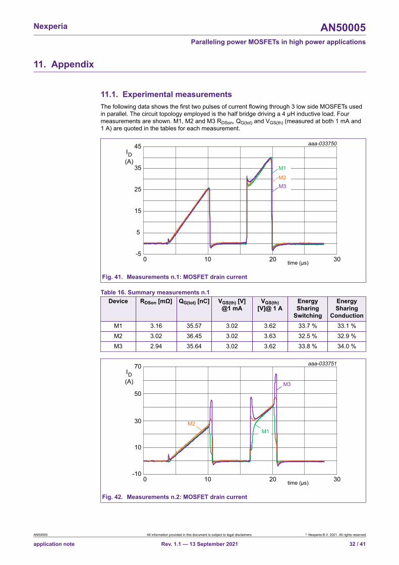
11.1. Experimental measurementsThe following data shows the first two pulses of current flowing through 3 low side MOSFETs usedin parallel. The circuit topology employed is the half bridge driving a 4 µH inductive load. Fourmeasurements are shown. M1, M2 and M3 RDSon, QG(tot) and VGS(th) (measured at both 1 mA and1 A) are quoted in the tables for each measurement.
aaa-033750
15
25
5
35
45I
-5
D(A)
M1
M2M3
time (µs)0 10 20 30
Fig. 41. Measurements n.1: MOSFET drain current
Table 16. Summary measurements n.1Device RDSon [mΩ] QG(tot) [nC] VGS(th) [V]
@1 mAVGS(th)
[V]@ 1 AEnergySharing
Switching
EnergySharing
ConductionM1 3.16 35.57 3.02 3.62 33.7 % 33.1 %M2 3.02 36.45 3.02 3.63 32.5 % 32.9 %M3 2.94 35.64 3.02 3.62 33.8 % 34.0 %
aaa-033751
30
50
10
70I
-10
D(A)
time (µs)0 10 20 30
M1M2
M3
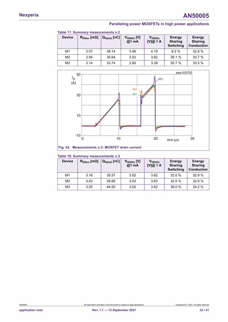
Fig. 42. Measurements n.2: MOSFET drain current
AN50005 All information provided in this document is subject to legal disclaimers. © Nexperia B.V. 2021. All rights reserved
application note Rev. 1.1 — 13 September 2021 32 / 41
Nexperia AN50005Paralleling power MOSFETs in high power applications
Table 17. Summary measurements n.2Device RDSon [mΩ] QG(tot) [nC] VGS(th) [V]
@1 mAVGS(th)
[V]@ 1 AEnergySharing
Switching
EnergySharing
ConductionM1 3.07 38.14 3.46 4.10 8.2 % 32.8 %M2 2.94 35.64 3.02 3.62 36.1 % 33.7 %M3 3.14 33.74 2.80 3.39 55.7 % 33.5 %
aaa-033752
30
50
10
I
-10
D(A)
time (µs)0 10 20 30
M1M2
M3
Fig. 43. Measurements n.3: MOSFET drain current
Table 18. Summary measurements n.3Device RDSon [mΩ] QG(tot) [nC] VGS(th) [V]
@1 mAVGS(th)
[V]@ 1 AEnergySharing
Switching
EnergySharing
ConductionM1 3.16 35.57 3.02 3.62 32.0 % 32.9 %M2 3.43 28.69 3.03 3.63 32.0 % 32.9 %M3 3.05 44.50 3.02 3.62 36.0 % 34.2 %
AN50005 All information provided in this document is subject to legal disclaimers. © Nexperia B.V. 2021. All rights reserved
application note Rev. 1.1 — 13 September 2021 33 / 41

Nexperia AN50005Paralleling power MOSFETs in high power applications
aaa-033753
30
50
10
70I
-10
D(A)
time (µs)0 10 20 30
M1
M3
M2
Fig. 44. Measurements n.4: MOSFET drain current
Table 19. Summary measurements n.4Device RDSon [mΩ] QG(tot) [nC] VGS(th) [V]
@1 mAVGS(th)
[V]@ 1 AEnergySharing
Switching
EnergySharing
Conduction
M1 3.16 35.57 3.02 3.62 25.5 % 33.2 %
M2 3.05 44.50 3.02 3.62 27.5 % 33.2 %
M3 3.14 33.74 2.80 3.39 45.3 % 33.6 %
11.2. SimulationsThe following simulations can be used to verify a SPICE model conformity to data sheet.
RDSon simulation
aaa-033728
M1
VGS0 V
ID25 ABUK7S1R0-40H
.inc BUK7S1R0-40H.lib.dc VGS 5 15 .1
Fig. 45. SPICE simulation circuit: RDSon check
AN50005 All information provided in this document is subject to legal disclaimers. © Nexperia B.V. 2021. All rights reserved
application note Rev. 1.1 — 13 September 2021 34 / 41

Nexperia AN50005Paralleling power MOSFETs in high power applications
GS5 15139 117
aaa-033756
1
1.8
R
0.6
(mΩ)
1.4
DSon
(V)V
Fig. 46. SPICE simulation circuit: RDSon as a function of VGS
QG(tot) simulation
aaa-033757
M1VGS
I2
ID
I1BUK7S1R0-40H
.inc BUK7S1R0-40H.lib.dc VGS 5 15 .1
D1
.subckt D_clamp anode cathode
.D1 anode cathode clamp_D.model clamp_D D(Rs=1e-6 Bv=Vdd Vj=Vf ibv=ID.ends.param Vdd=32 ID=25 Vf=1
PULSE(0 1m 1n 1n 1n 200u 400u 1)
D_clamp
Fig. 47. SPICE simulation circuit: QG(tot) check
AN50005 All information provided in this document is subject to legal disclaimers. © Nexperia B.V. 2021. All rights reserved
application note Rev. 1.1 — 13 September 2021 35 / 41

Nexperia AN50005Paralleling power MOSFETs in high power applications
time (µs)0 161284
aaa-033758
8
4
12
16GS
0
(V)
V
Note: the charge can be found by multiplying the horizontal axis by 10-3 C/s.
Fig. 48. SPICE simulation circuit: VGS as a function of time
VGS(th) simulation
aaa-033759
M1
VGS0 V
VDS12 V
BUK7S1R0-40H
.inc BUK7S1R0-40H.lib.dc VGS 2.3 3.3 .01
Fig. 49. SPICE simulation circuit: VG(th) check
aaa-03376016
02.2 3.42.6 3.0
12
8
4
I
V
D(mA)
GS (V)
Fig. 50. SPICE simulation circuit: VG(th) check
AN50005 All information provided in this document is subject to legal disclaimers. © Nexperia B.V. 2021. All rights reserved
application note Rev. 1.1 — 13 September 2021 36 / 41

Nexperia AN50005Paralleling power MOSFETs in high power applications
12. References1. “The Art of Electronics”, by Paul Horowitz and Winfield Hill: §3.6.3. Paralleling MOSFETs, page.
2132. AN90011: Half-bridge MOSFET switching and its impact on EMC3. AN90003: LFPAK MOSFET thermal design guide”4. BUK7S1R0-40H data sheet
13. Revision historyTable 20. Revision historyRevisionnumber
Date Description
1.1 2021-09-13 Minor update, values corrected in Table 12 and Table 14.1.0 2021-09-07 Initial version.
AN50005 All information provided in this document is subject to legal disclaimers. © Nexperia B.V. 2021. All rights reserved
application note Rev. 1.1 — 13 September 2021 37 / 41

Nexperia AN50005Paralleling power MOSFETs in high power applications
14. Legal information
DefinitionsDraft — The document is a draft version only. The content is still underinternal review and subject to formal approval, which may result inmodifications or additions. Nexperia does not give any representations orwarranties as to the accuracy or completeness of information included hereinand shall have no liability for the consequences of use of such information.
DisclaimersLimited warranty and liability — Information in this document is believedto be accurate and reliable. However, Nexperia does not give anyrepresentations or warranties, expressed or implied, as to the accuracyor completeness of such information and shall have no liability for theconsequences of use of such information. Nexperia takes no responsibilityfor the content in this document if provided by an information source outsideof Nexperia.
In no event shall Nexperia be liable for any indirect, incidental, punitive,special or consequential damages (including - without limitation - lostprofits, lost savings, business interruption, costs related to the removalor replacement of any products or rework charges) whether or not suchdamages are based on tort (including negligence), warranty, breach ofcontract or any other legal theory.
Notwithstanding any damages that customer might incur for any reasonwhatsoever, Nexperia’s aggregate and cumulative liability towards customerfor the products described herein shall be limited in accordance with theTerms and conditions of commercial sale of Nexperia.
Right to make changes — Nexperia reserves the right to make changesto information published in this document, including without limitationspecifications and product descriptions, at any time and without notice. Thisdocument supersedes and replaces all information supplied prior to thepublication hereof.
Suitability for use — Nexperia products are not designed, authorized orwarranted to be suitable for use in life support, life-critical or safety-criticalsystems or equipment, nor in applications where failure or malfunctionof an Nexperia product can reasonably be expected to result in personalinjury, death or severe property or environmental damage. Nexperia and itssuppliers accept no liability for inclusion and/or use of Nexperia products insuch equipment or applications and therefore such inclusion and/or use is atthe customer’s own risk.
Applications — Applications that are described herein for any of theseproducts are for illustrative purposes only. Nexperia makes no representationor warranty that such applications will be suitable for the specified usewithout further testing or modification.
Customers are responsible for the design and operation of their applicationsand products using Nexperia products, and Nexperia accepts no liability forany assistance with applications or customer product design. It is customer’ssole responsibility to determine whether the Nexperia product is suitableand fit for the customer’s applications and products planned, as well asfor the planned application and use of customer’s third party customer(s).Customers should provide appropriate design and operating safeguards tominimize the risks associated with their applications and products.
Nexperia does not accept any liability related to any default, damage, costsor problem which is based on any weakness or default in the customer’sapplications or products, or the application or use by customer’s third partycustomer(s). Customer is responsible for doing all necessary testing for thecustomer’s applications and products using Nexperia products in order toavoid a default of the applications and the products or of the application oruse by customer’s third party customer(s). Nexperia does not accept anyliability in this respect.
Export control — This document as well as the item(s) described hereinmay be subject to export control regulations. Export might require a priorauthorization from competent authorities.
Translations — A non-English (translated) version of a document is forreference only. The English version shall prevail in case of any discrepancybetween the translated and English versions.
TrademarksNotice: All referenced brands, product names, service names andtrademarks are the property of their respective owners.
AN50005 All information provided in this document is subject to legal disclaimers. © Nexperia B.V. 2021. All rights reserved
application note Rev. 1.1 — 13 September 2021 38 / 41

Nexperia AN50005Paralleling power MOSFETs in high power applications
List of TablesTable 1. Summary - Ideal case: equal MOSFETs................ 6Table 2. BUK7S1R0-40H data sheet characteristics:RDSon.................................................................................. 7Table 3. SPICE model mod for RDSon spread....................7Table 4. Summary - Effects of RDSon spread..................... 8Table 5. BUK7S1R0-40H data sheet characteristics:gate charge.......................................................................... 8Table 6. SPICE model mod for QG(tot) spread................... 9Table 7. Summary - Effects of QG(tot) spread...................10Table 8. BUK7S1R0-40H data sheet characteristics:VGS(th)...............................................................................10Table 9. SPICE model mod for VGS(th) spread.................10Table 10. Summary - Effects of VGS(th) spread................11Table 11. Summary - Effects of VGS(th) batch spread.......17Table 12. Summary - sharing without gate resistorsplit: RG = 39 Ω.................................................................19Table 13. Summary - sharing with gate resistor split:RG,drv = 12 Ω and RG,split = 3.9 Ω................................. 19Table 14. Summary – comparison of sharing with andwithout gate resistor split................................................... 19Table 15. Summary – sharing with a source resistor of1 mΩ...................................................................................21Table 16. Summary measurements n.1............................. 32Table 17. Summary measurements n.2............................. 33Table 18. Summary measurements n.3............................. 33Table 19. Summary measurements n.4............................. 34Table 20. Revision history..................................................37
AN50005 All information provided in this document is subject to legal disclaimers. © Nexperia B.V. 2021. All rights reserved
application note Rev. 1.1 — 13 September 2021 39 / 41
Nexperia AN50005Paralleling power MOSFETs in high power applications
List of FiguresFig. 1. SPICE simulation circuit: half-bridge.........................3Fig. 2. MOSFETs drain current (ID) and energydissipation (Ediss) - ideal case: equal MOSFETs. Theturn-ON, conduction and turn-OFF phases are indicated.... 4Fig. 3. MOSFETs drain current (ID), energy dissipation(Ediss) and power dissipation (Pdiss) - ideal case:equal MOSFETs. The turn-ON phase is indicated............... 5Fig. 4. MOSFETs drain current (ID), energy dissipation(Ediss) and power dissipation (Pdiss) - ideal case:equal MOSFETs. The turn-OFF phase is indicated............. 5Fig. 5. BUK7S1R0-40H sub-threshold drain current asa function of gate-source voltage........................................ 7Fig. 6. MOSFETs drain current (ID) - effects of RDSonspread...................................................................................8Fig. 7. Gate charge waveform definitions............................ 9Fig. 8. MOSFETs drain current (ID) - effects of QG(tot)spread.................................................................................10Fig. 9. MOSFETs drain current (ID) - effects ofVGS(th) spread.................................................................. 11Fig. 10. MOSFET electrical-thermal interaction................. 12Fig. 11. BUK7S2R5-40H data sheet graph: transfercharacteristic ZTC point..................................................... 12Fig. 12. BUK7S2R5-40H data sheet graph: normalizedon-state resistance as a function of junction temperature..13Fig. 13. SPICE simulation circuit: thermal coupling........... 13Fig. 14. Thermal coupling influence on sharing:RDSon(M1) = 0.62 mΩ and RDSon(M2) = 1 mΩ...............14Fig. 15. BUK7S1R0-40H data sheet graph: gate-source threshold voltage as a function of junctiontemperature........................................................................ 15Fig. 16. VGS(th) batches spread for BUK7S1R5-40H....... 16Fig. 17. Absolute value of the difference in VGS(th)between two consecutive devices......................................16Fig. 18. MOSFETs drain current (ID) – data sheet andbatch VGS(th) spread comparison.....................................17Fig. 19. SPICE simulation circuit: gate resistor splitcomparison......................................................................... 18Fig. 20. Gate-source voltage without and with gateresistor split........................................................................ 18Fig. 21. MOSFETs drain current (ID) – without gateresistor split........................................................................ 18Fig. 22. MOSFETs drain current (ID) – with gateresistor split........................................................................ 19Fig. 23. SPICE simulation circuit: source resistors............ 20Fig. 24. MOSFETs drain current (ID) – with a sourceresistor of 1 mΩ................................................................. 21Fig. 25. MOSFETs drain current (ID) – effects ofsource resistor value..........................................................21Fig. 26. MOSFETs drain current (ID) - effects ofparasitic inductance........................................................... 22
Fig. 27. Effects of higher parasitic inductance on lowside VDS at turn-OFF........................................................ 23Fig. 28. MOSFETs drain current (ID) - effects ofparasitic inductance imbalance..........................................23Fig. 29. Gate-source loop: possible layout.........................24Fig. 30. Half-bridge layout possibilities showinginductances........................................................................ 24Fig. 31. CFD simulation setup........................................... 25Fig. 32. CFD current density simulation: Low sideMOSFETs ON – Top side.................................................. 26Fig. 33. CFD current density simulation: Low sideMOSFETs ON – Bottom side.............................................26Fig. 34. CFD current density simulation: High sideMOSFETs ON – Top side.................................................. 27Fig. 35. Speeding up turn-OFF switching.......................... 27Fig. 36. SPICE simulation circuit: measure ofMOSFET dissipated power................................................ 29Fig. 37. Worst case simulation combinations -MOSFET drain current (ID)................................................29Fig. 38. Worst case simulation combinations -MOSFET average power................................................... 29Fig. 39. Worst case simulation combinations -MOSFET average power................................................... 30Fig. 40. SPICE simulation MOSFET temperatures check..30Fig. 41. Measurements n.1: MOSFET drain current.......... 32Fig. 42. Measurements n.2: MOSFET drain current.......... 32Fig. 43. Measurements n.3: MOSFET drain current.......... 33Fig. 44. Measurements n.4: MOSFET drain current.......... 34Fig. 45. SPICE simulation circuit: RDSon check................34Fig. 46. SPICE simulation circuit: RDSon as a functionof VGS................................................................................35Fig. 47. SPICE simulation circuit: QG(tot) check............... 35Fig. 48. SPICE simulation circuit: VGS as a function oftime.....................................................................................36Fig. 49. SPICE simulation circuit: VG(th) check.................36Fig. 50. SPICE simulation circuit: VG(th) check.................36
AN50005 All information provided in this document is subject to legal disclaimers. © Nexperia B.V. 2021. All rights reserved
application note Rev. 1.1 — 13 September 2021 40 / 41
Nexperia AN50005Paralleling power MOSFETs in high power applications
Contents1. Introduction...................................................................22. Applications.................................................................. 23. Key specifications........................................................ 24. MOSFET dissipation and parameters' influenceon current sharing............................................................. 45. Influence of parameter spread on currentsharing performance......................................................... 65.1. Static operation (DC)...................................................75.1.1. Drain-source on-state resistance – RDSon.................75.2. Dynamic operation.......................................................85.2.1. Total input charge – QG(tot)....................................... 85.2.2. Gate-source threshold voltage – VGS(th)................. 105.3. Paralleled MOSFETs and temperature dependency.. 125.3.1. Temperature dependency during staticoperation (DC)....................................................................135.3.2. Temperature dependency during dynamicoperation.............................................................................145.4. Data sheet and batch spreads.................................. 156. Circuit optimisation.................................................... 176.1. Localized gate resistor...............................................176.2. Components in the source path.................................207. PCB layout influence..................................................227.1. Layout-dependent parasitics......................................227.2. Circuit layout..............................................................238. Driving paralleled MOSFETs......................................279. Simulation tools..........................................................2810. Conclusion................................................................ 3111. Appendix....................................................................3211.1. Experimental measurements................................... 3211.2. Simulations...............................................................3412. References................................................................ 3713. Revision history........................................................3714. Legal information......................................................38
© Nexperia B.V. 2021. All rights reservedFor more information, please visit: http://www.nexperia.comFor sales office addresses, please send an email to: [email protected] of release: 13 September 2021
AN50005 All information provided in this document is subject to legal disclaimers. © Nexperia B.V. 2021. All rights reserved
application note Rev. 1.1 — 13 September 2021 41 / 41