parameter calibration of drift-diffusion model in quasi ... · parameters of drift-diffusion (dd)...
TRANSCRIPT

����
Parameter Calibration of Drift-Diffusion Model in Quasi-Ballisitc Transport Region with Monte Carlo Method
Lei Shen, Shaoyan Di, Longxiang Yin, Xiaoyan Liu and Glillgl)ll Institute of Microelectronics, Peking University, Beijing, China
Email: [email protected]
Abstnret - As the device scaling down to sub-10nm, the quasi-ballistic transport become. important. Some previous works have suggested using DD method to involve the quasi-ballistic transport effect through modifying the transport parameters. A procedure is introduced to calibrate the transport parameters of the DD model by using the simulation r .. nlts of Me device simulator.
I. INTRODUCTION
As the device scaling down to sub-IOnm, the quasiballistic transport phenomenon strongly affects the device characteristics [1]. The usage of steady-state transport parameters of drift-diffusion (DD) method may not get correct carriers velocity distributions. The full band Moote Carlo (MC) method can investigate the quasi-ballistic transport [2], but it is very time consuming. Some previous works have suggested using DO method through modifYing the transport parameters of the DD model [3, 4]. In this work, we will introduce a procedure to calibrate the transport parameters of the DD model by using the simulation results of MC device simulator to involve the quasi-ballistic transports effect. A 200m gate length device will be calibrated as an example.
IT. CALIBRATION METHOD
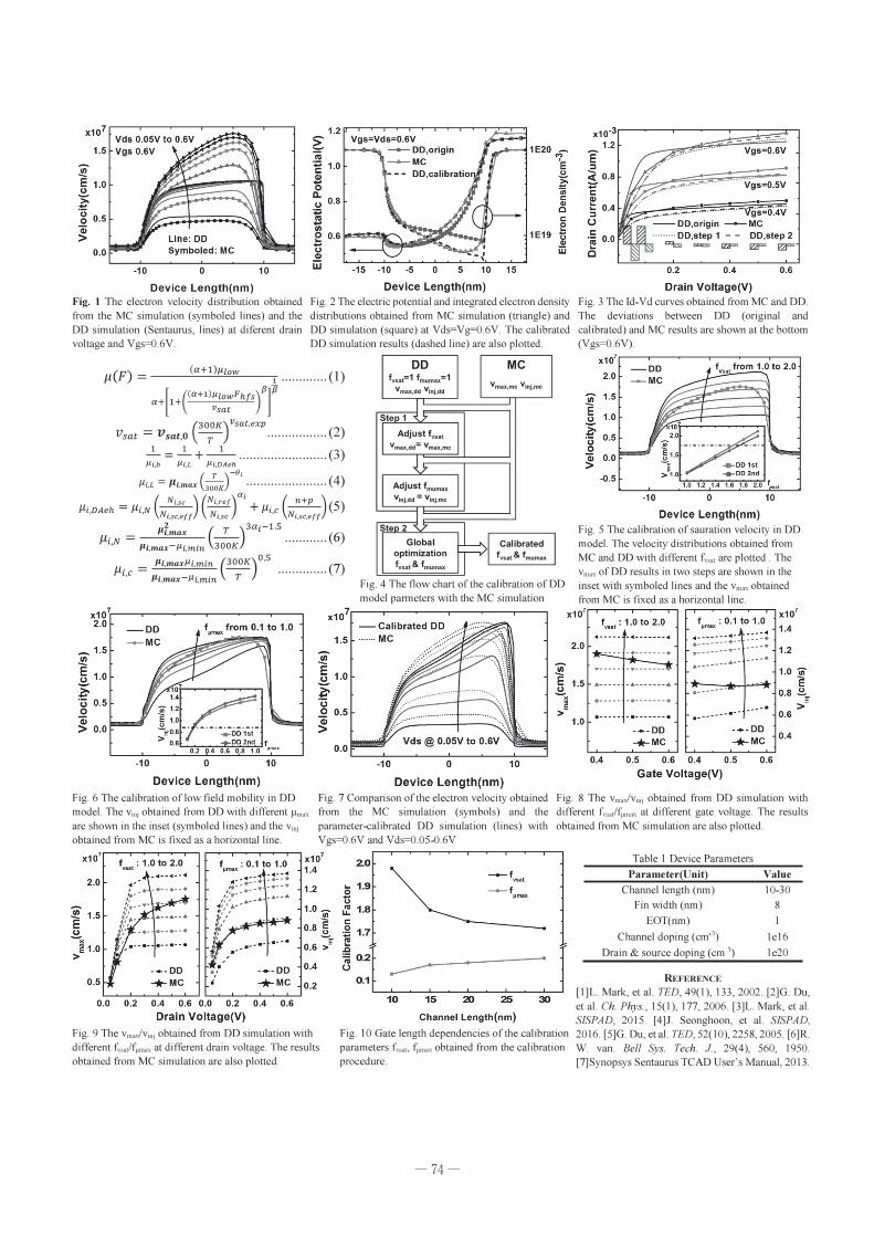
A full-band ensemble Moote Carlo simulator [2, S] taking into account the major scattering mechanisms including phonon scattering, impact ionization scattering, and ionized impurity scattering is used to calibrate the OD model. DriftDiffusion method is widely used to describe semiconductor devices [6]. In the typical commercial TCAD tool based on the OD model, such as Sentaurus TCAD [7], the transport models include low field effective mobility (1'<», high field saturation model (eq.(I), eq.(2», Philips unified mobility model (eq.(3)-eq.(7), ete. A 20 run FinFET is simulated by DD and MC method, and the structure parameters are listed in Tahle 1. The distributions of electron velocity, electron density and electric potential are plotted in Fig. 1 and Fig. 2. In the MC simulation results, the electron velocity shows significant overshoot effects at high drain biases, while in the DD method results, the electron velocity saturates and looks almost the same on different high drain biases. The limitation of transport model in DD model leads to the difference in carrier density distributions and currents as shown in Fig. 2 and Fig. 3.
The transport parameters calibration procedure is proposed as shown in Fig. 4. Two target variables (v""", Vi.j)
and two calibration parameter factors (f_, f._) are considered. In the step I, the f_ (a multiplication mctor of the saturation velocity, as mentioned in eq.(l), eq.(2» is first adjusted to match the V_dd with vm""",,(the maximum velocity in the channel). Then the f""", (a multiplication Ii!.ctor of"""" which represent the low-field mobility in the channel in the Philips unified mobility model as mentioned in eq.(3)eq.(7) is adjusted to match the Vinj.dd with Vmj.= (the velocity at the top of the barrier in the channel) using the selected f_. I .
In the step 2, a global optimization is carried out to optimize the fVliat and flUllax•
ill. REsULTS AND DISCUSSION
A 20nm gate length double gate transistor is used to verifY the calibration method as an example. First, a set off~" from 1.0 to 2.0 is chosen, and the velocity distributions obtained from the DO method are shown in Fig. 5. The maximum velocity versus fwot are plotted in the inset. The velocity saturation model sets a limit to the maximum velocity, while electrons with quasi-ballistic transport filature will break the limitation as the Monte Carlo simulation shows in Fig. 1. The f_" ~ 1.66 is chosen at the intersection in the inset in Fig. 5 to match the V_dd and v_=. Then a set off ..... from 0.1 to 1.0 with fw"~ 1.66 is taken into DD simnlation, and the velocity distributions are obtained from the DO method as shown in Fig. 6. The parameter """"in Philips unified mobility model controls the low-field mobility in the channel region. As the maximum velocity is limited by the parameter v .. , 11m~ mainly cbanges the velocity near the source region. As a key parameter in quasi-ballistic transport, the velocity at the top of barrier, also called injection velocity, is chosen as the target variable. The injection velocity versus f"""" are plotted in the inset and fllJIlwc,sl=O.19 is chosen to match the Vinj,dd and Vinj,mco As we can see in Fig. 6, the fiJ!ll&X has some effect on Vmu., therefore a global optimization is necessary. The adjustment off_", in step two uses f""""'1 instead ofl.O, followed by the calibration of the f"""",,,. Then the final calibration mctors f_",~1.75 and f""""",={l.IS are obtained. The electron velocity distributions with diffurent drain voltage calculated with parameter-calibrated DD model and MC method are plotted in Fig. 7, which are closer to each other and the key parameters v_ and Vinj are mainly fitted. As shown in Fig.2 and Fig. 3, the distributions of electron density, potential and I-V curves obtained from parameter-calibrated DD model are closer to the MC method.
Fig. 8 and Fig. 9 shows the variation of the key parameters with the gate voltage and drain voltage. The same trends represent the same calibration factor values. With the decrease of gate voltage, both the f_ and f._ have a little rising trend. The f""", fits well with the drain voltage decrease, while the fwo! drops especially at low drain voltage. The gate length dependencies of the calibration mctors obtained from the calibration method are shown in Fig. 10. As the gate length decreased, the saturation velocity (v",) is increasing while the low-field mobility (J!m~) is reduced, which is closer to the characteristics of quasi-ballistic transport
IV. CONCLUSION
The two step calibration procedure is introduced. The parameter-calibrated DD method is more accurate than original model and more efficient than MC method. The device filatures obtained from the parameter-calibrated DD model fit well with MC simulator. The trends of calibration factors are also investigated with the variation of drain voltage, gate voltage and gate length.
AcKNOWLEDGEMENT
This work is supported by the National High-tech R&D Program (863 Program) 2015AAOl6501.
����
x107 r--~---~----~----'
I.'
.!!! § 1.0
~ g 0.5
~
-10
Lin e: DO Symboled : Me
Device Length(nm)
10 -15 -1 0 -. • 10
Device Length(nm)
I.
1E20 M 'E
*: ~ • c ~ c e
1E1 9 ~ iii
Fig. 1 The electron velocity distribution obtained from the MC simulation (symboled lines) and the DD simulation (Scntaurus, lines) at diferent drain voltage and VWF'J.6V.
Fig. 2 The electric potential and integrated electron density distributions obtained from MC simulation (triangle) and DD simulation (square) at Vds=Vg=O.6V. The calibrated DD simulation results (dashed line) are also plotted.
( ) (a+1)"low P F = 1 ............. (1)
«+[1 +CaH):::;FhIS) P]J (300~ l1sat,ltxp
V.a, = ".a,.O -T--) ................. (2) ..!c..=..!c..+_' _ ......................... (3) Jl.f,b 1lt,L IlI,DA.h
Jl!,L = I'~C:OK)-61 ....................... (4)
Ilt,DAeh = /l1,N (NNI,IC ) (NNt.r.r)ai + Ilt,c (Nn+p )(5)
l.s~ff f.sc /..sc"ff
,,' ( T )3«1-1.5 PiN = 1.- -- ............ (6)
, I".maz-Ili,mfn 300K
_ Il1.fftlUI'tmtn (300K)0.s PIc - .............. (7)
, I£tfftllZ-I't.m1n T
X1 07·,_~ __ -_--_-~---, 2.0
_1 .5 .!!! 5 1.0
~ ·0 0.5 o ~
-DO f...,.,x from 0.1 to 1.0
'~~ A:: E 1.0 ~fO .8 -. ·-·- · -~oo ·1;i -> 0.6 DO 2nd f
0.2 .4 0.6 0.8 1.0 , ....
-10 o 10
Device Length(nm)
1.5
~ 5 1.0
~ ·u ..Q 0.5
:l!
DO Me ' • ..=1 flllu_=1
v-.-y~ y .......... y~ ....
I Sto 1
AdjustfYat v_~ .. = v .........
.& AdJustf
lllu_
v .......... vlllJ ....
2
Glo'" H c.m ...... optlmlutlon '¥HI& 'II1II_ fv.t&f
IllM_
Fig. 4 The flow chart of the callbratJ.on ofDD model parmeters with the Me simulation
-10 o 10
Device Length(nm)
X1~.:'-==:;::::;~;;;~~~C~·· · ·~:7.·~· · l E ~ Vgs=0.6V
~ « 0." 'l ~ 0.4 ~
U
.~ 0.0
c
.......... "' .. "' .. .. \igs=0.5V .I /"
/ .. _ .. _ .. -.. -.. -.. -.. - .. -.. -.. - .-vg~J . ...... .. --DD.origin - Me
.. ........ DD.step 1 - - DD,step 2 "9r::!:I IZlJII3' I?1F E'.a'"'"
0.2 0.4 0 .•
Drain Voltage(V) Fig. 3 Theld-Vd curves oblained from MC and DD. The deviations between DD (original and calibrated) and Me results are shown at the bottom (Vgs=O.6V).
X101,-~-~-~---~---,
tV
"1 f rom 1.0 to 2.0
2.0
~ 1.5
5 1.0 ~ U 0.5 o ~
- DO _ MC
Device Length(nm) Fig. 5 The calibration of sauration velocity in DD model. The velocity distributions obtained from Me and DD with different f'lllt are plotted. The Vmax ofDD results in two steps are shown in the inset with symboled lines and the Vrux obtained from Me is fixed as a horizontal line
f : 0 .1101 .0 "~,
' _ 1. 1.0 to 2.0 1 .4
::~::::::: : ::::: 1.2 ....... -.. -----_ ..
2.0 -*'"=- __ . _+_ •• ____ +
.----- -.------'" ."'-' .--_ ...
0 .4
- - - DO
+ MC
.-.- --_ .. -.. _.-- _ _ DO
+ MC
0 .5 0 .6 0.4 0.5 0 .•
Gate Voltage(V)
1.0 ~
0.8 ~"!'" >-
0 .•
0.4
Fig. 6 The calibration of low field mobility in DD model. The Vinj obtained from DD with different J.Imax are shown in the inset (symboled lines) and the v~ obtained from MC is :fixed as a horizonta1line.
Fig. 7 Comparison of the electron velocity obtained from the Me simulation (symbols) and the paramcter-cal.ibrated DD simulation (lines) with Vgs=O.6V and VdRl.05-O.6V
Fig. 8 The vm.rlViJJ.j obtained from DD simulation with different f-/f..,- at diffcrCIII: gate voltage. The results obtained :from Me simulation are also plotted.
X107 ,~. : 1 .0 to 2.0 1 : 0.1 to 1.0 x10⁷
"- , 1.4 2.0
1.2
~
/~:::::: ::::: f; 1.0 __
I.' E f - - 0." .!:!. h o ~ .. ,_ .. _. _.--
0 .• >
- ... · 00 . . __ _ 00 0.4 .. +MC • + MC 0.2
0 .0 0.2 0.4 0.6 0.0 0.2 0.4 0.6 Drain Voltage(V)
Fig. 9 The vrrw/viDj obtained from DD simulation with different Uf,...... at different drain voltage. The resul1li obtained from MC simulation are also plotted.
~ u
~
2.0
~ 1.9
:. 1.8 c ~ 1.7 E
.Q
~ 0.2 u
0.1
10 15
_I ,. ,
25 30
Table 1 Device Parameters Parameter(UDit)
Channe11ength (run) Fin width (run)
BOT(nm) Channel doping (enr')
Drain & source doping (cm-3)
REFERENCE
Value H)-30
8
1e16 1020
[l]L. Marle, et al. TED, 49(1),133,2002. [2]G. Du, et al. Ck Phys., 15(1), 177,2006. [3]L. Marle, et al.
Channel Length(nm) SISPAD, 2015. [4]J. Seonghoon, et al. SISPAD, Fig. 10 Gate length dependencies of the calibration 2016. [5]G. Do, et al. TED, 52(10), 2258, 2005. [6]R. parameters f_f_obtained from the calibration w. van. Bell Sys. Tech. J., 29(4), 560, 1950. procedure. [7]Synopsys Sentaurus TCAD User's Manual. 20l3.