passive integration
TRANSCRIPT
7/28/2019 Passive Integration
http://slidepdf.com/reader/full/passive-integration 1/26
7/28/2019 Passive Integration
http://slidepdf.com/reader/full/passive-integration 2/26
Passive Integration Seminar Report ’03
Passive integration suggests that if the passives were so small and flat,
then they could be inserted between layers of the circuit board itself, rather than
taking space on top of it. The electronic devices could be thinner and sleeker
than they are today, or they could contain more electronics, or if it is a phone can
have much larger batteries and therefore longer talk time and brighter color
screens. The same goes for almost every device from PDAs to portable DVD
players.
The integrated passives would be a part of the circuit board itself, formed
when the board was, so odds are good that their overall cost could eventually be
less than what manufacturers pay today to buy and solder on discrete devices.
Speaking of solder, eliminating it is another advantage of integration, because
bad solder joints are one of the most common reasons electronic gear fails. Less
solder also means less harm from lead waste.
The list of advantages goes on: putting the passives "underground" leaves
more room on the surface of the board for ICs, which means more design
flexibility. And there are electrical benefits, too. Because current travels along a
different path in integrated capacitors than in surface-mounted components,
integrated capacitors can be made freer of the trace amounts of the inductance,
called parasitic inductance, that plagues any capacitor and limits usefulness in
high-frequency circuits. Finally, because the components are custom-made whenthe board is, the resistors, capacitors, and inductors can be sized to any desired
value, rather than being chosen from a manufacturer's list of available parts.
Advantages like these point to a potentially huge shift for the electronics
industry. Over a trillion passive components were bonded to boards last year,
according to the National Electronics Manufacturing Initiative's road map. These
devices are minuscule, and that makes putting them in place a chore. The
Dept. of ECE MESCE Kuttippuram2
7/28/2019 Passive Integration
http://slidepdf.com/reader/full/passive-integration 3/26
Passive Integration Seminar Report ’03
smallest discrete passives today measure 0.50 mm by 0.25 mm; spread on a
sheet of paper, they'd look like ground pepper. Such compact components are
difficult to handle and attach, even for automated assembly equipment. And
though the total cost of each part—including capital, assembly, and the prorated
cost of the underlying board—is less than two cents on average, collectively the
impact of integrated passives on system cost, reliability, and, most of all, size,
could be enormous.
But for these passives to make a big dent in the US $18-billion-a-year
market for discrete passive components, makers of circuit boards will have to
reposition themselves as purveyors of passive electronic networks. It's starting to
happen, but slowly. Such manufacturers as Gould, Shipley, Ohmega,
MacDermid, DuPont, Oak-Mitsui, 3M, and Sanmina all market products and
processes for integrating resistors directly into printed-circuit boards, using at
least four different technologies; and for integrating capacitors, using at least
five. These sizable companies have all poured tens of millions of dollars in R&D
funds into proving the concept. In the meantime, several other companies,
including California Micro Devices Corp. and AVX Corphave been working on
an alternative approach to integrating passives. They are selling arrays and
networks of miniaturized passive devices in single IC-like packages.
In a sense, the situation with passive components today is a lot like that of
active devices 40 years ago, when Intel, Fairchild, and others had just introducedICs that combined active devices like transistors and diodes on a single
substrate. But don't expect Moore's Law to apply to passives. These components
cannot be scaled down into the submicron realm occupied by active devices. The
reason, of course, is that passive components have to handle signals whose
amplitude cannot be reduced arbitrarily—say, microwave signals going to a
cellphone antenna or inputs for analog-to-digital conversion. Despite this
fundamental limit, passive integration will make for much more miniaturization.
Dept. of ECE MESCE Kuttippuram3

7/28/2019 Passive Integration
http://slidepdf.com/reader/full/passive-integration 4/26
Passive Integration Seminar Report ’03
NEED FOR PASSIVE INTEGRATION
Passive components refer to such kind of electrical components that
cannot generate power. Typical components are resistors, capacitors and
inductors. The primary functions of passive components are to manage buses,
bias, decouple Ics, by-pass, filter, tune, convert, and sense and protect. It is a
huge, multi-billion business, supporting the various electronic products in
automotive, telecommunications, computer and consumer industries, both for
digital and analog-digital applications. There are a large number of passive
components that are used in consumer electronic products such as VCRs,
camcorders, television tuners, and other communication devices. Most of the
passive components nowadays are discrete surface mount passive components
that directly mount on the surface of the printed circuit board. It is called as
discrete passive component-a singular component enclosed in a single case that
must be mounted to an interconnecting substrate. Passive components are
commonly referred to as “glue components” since they “glue” integrated circuits
together to make the system.
Surface mount technology was starting to take deep root in our industry
in early 80’s and is fully developed till today. In the early days, surface mount
components were many times more expensive than through hole componentsand new surface mount assembly equipment costs were off the charts. As time
went on, the cost of the components, assembly equipment and all of the other
infrastructure came down, today it is less expensive to build a surface mount
assembly than a through hole assembly. However, the faster bus speeds required
new technology. PCB traces have always had transmission line characteristics
and are more sensitive at subnano-second rise times. The package lead
inductance and line capacitance have greater impact on signal integrity. The
Dept. of ECE MESCE Kuttippuram4
7/28/2019 Passive Integration
http://slidepdf.com/reader/full/passive-integration 5/26
Passive Integration Seminar Report ’03
integrated circuit industry is achieving faster speeds by shrinking technology; it
follows that the passive solution must also shrink. In addition to these, the need
to drive out every cent of costs, miniaturization, improved product reliability and
the passive to active ratios have caused to seriously consider much higher levels
of passive integration than in the past. Then comes the idea of integral passives.
Integral passives are noted as passive components embedded within or on
the surface of a substrate. These are distinguished from discrete chips and also
from integrated(multiple passive functionality within a single package).It is a
part of the printed circuit board using some type of material to make resistors,
capacitors or inductors. The requirement for integral resistors, capacitors and
inductors are:
Resistors:
A primary requirement for integral resistors is that they be size competitive
with the chip resistor. It dictates that the largest dimension be of the order of
1.0mm.Cost considerations dictate that trimming should not be required to
obtain a 5%-10% tolerance. The range of values used,from one ohm to one
mega-ohm dictates that if that range was implemented there would be
insufficient numbers in the tails of the value distribution to justify integrating the
full range.
Capacitors:
Discrete capacitors are used in larger number and greater density than any
other discrete passive component. There are atleast two distinct application
potentials for integration, one in which the polymer or ceramic board itself
provides dielectric and capacitor plates within the interconnection; and the
second, wherein progressively higher dielectric constant materials make
Dept. of ECE MESCE Kuttippuram5
7/28/2019 Passive Integration
http://slidepdf.com/reader/full/passive-integration 6/26
Passive Integration Seminar Report ’03
increasingly larger capacitance feasible. There is a possibility to eliminate about
40% of the discrete capacitors in a hand held product by simply designing low
value capacitors into one or more of the two level interconnection patterns
normally used.
Inductors:
Inductors are currently used in such low quantities,that the equivalent per part
cost will probably be too high to incorporate any special processes or materials.
High values are best attained with conventional discrete parts.However,about
80% of the inductors used in a hand held product are low enough in value, that
they can be incorporated directly into wiring of a suitable substrate.They require
fine line capability small vias and thin dielectrics.Careful attention to design will
be necessary due to coupling to nearby metal..
History is repeating itself using the same benefits and arguments,the bottom
line is embedded passives.
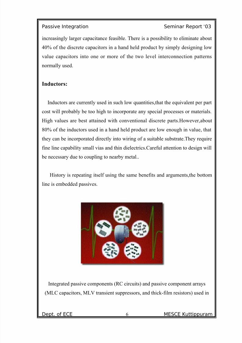
Integrated passive components (RC circuits) and passive component arrays
(MLC capacitors, MLV transient suppressors, and thick-film resistors) used in
Dept. of ECE MESCE Kuttippuram6

7/28/2019 Passive Integration
http://slidepdf.com/reader/full/passive-integration 7/26
Passive Integration Seminar Report ’03
medical electronics
COMPARISON BETWEEN EMBEDDED
AND DISCRETE PASSIVES
The generic single board computer ,nowadays is generally composed of
5% integrated circuits,4% connectors,40% capacitors,33% resistors and 18%
miscellaneous parts.Clearly resistors and capacitors are the majority of
components on any generic PCB.The target is to reduce the number of SMT
resistors from 33% of the total components to 10%, increase the yield, while
allowing the designers better signals and more surface real estate. The obvious
advantages that embedded passives have over discrete passives are in size,
weight, cost and performance. First, the discrete passives, though occupy various
space in various product, will occupy at a minimum of 5% of the surface area,
which can be saved by using embedded passives. Then,when the number of
passive components is large, the cost of conversion to place surface mount
passive components will be quite large, including purchase, stocking, placement,
test, repair and warranty service. But for embedded passives, it can be reduced
by some sort of parallel process. The third, surface mount resistors and
capacitors have inherent parasitic functionalities, due to their geometries.
Perhaps the most important is the parasitic inductance associated with the
capacitors. This inductance affects performance at high frequency, and thus
limits digital signaling rates. On the contrary, embedded passives should reduce
or eliminate the parasitics associated with the current passive packages. Besides,
there are some intangible benefits for embedded passives. Improved wireability,
higher reliability, reduction in part numbers, higher throughput in manufacturing
assembly and increased yield in manufacturing assembly. The improved
wireability is feasible based on personal experience. The reduction in part
Dept. of ECE MESCE Kuttippuram7
7/28/2019 Passive Integration
http://slidepdf.com/reader/full/passive-integration 8/26
Passive Integration Seminar Report ’03
numbers is all readily apparent, it remains to be seen what impact there is on a
large scale. The reliability, throughput and yield all need to proven before any
real credibility can be given.
On the other hand, integral passives have limits too. They cannot provide
wide range of resistor values. And tight tolerances are needed on their values.
This also exists for embedded capacitors. In addition to these, the embedded
passives need to hold their values over time and temperature. To solve these
problems, new materials and low cost processes are needed for embedded
passive technology. The last problem is that even simple engineering changes
cannot be made to an integral passive substrate. Therefore consistent and rapid
turnaround of prototype designs is needed for fabricators.
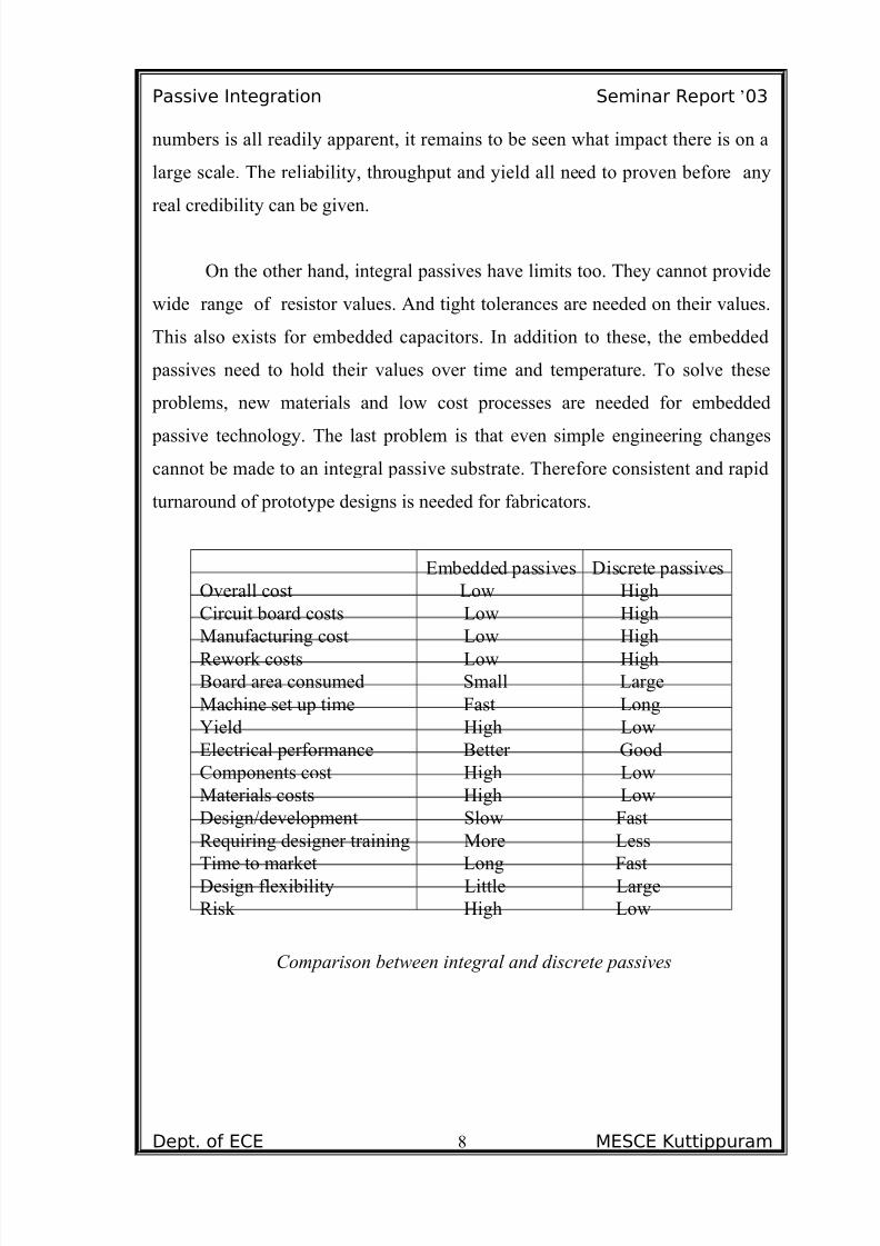
Embedded passives Discrete passives
Overall cost Low High
Circuit board costs Low High
Manufacturing cost Low High
Rework costs Low HighBoard area consumed Small Large
Machine set up time Fast Long
Yield High Low
Electrical performance Better Good
Components cost High Low
Materials costs High Low
Design/development Slow Fast
Requiring designer training More Less
Time to market Long Fast
Design flexibility Little Large
Risk High Low
Comparison between integral and discrete passives
Dept. of ECE MESCE Kuttippuram8

7/28/2019 Passive Integration
http://slidepdf.com/reader/full/passive-integration 9/26
Passive Integration Seminar Report ’03
INTEGRATED PASSIVE TECHNOLOGY
The technologies available for the packaging of microelectronics at thattime were generally thick film and thin film circuits hermetically sealed in a
package made of ceramic or metal with glass to metal feed-throughs. The need
for a package, interconnect board plus discrete components complicated the
assembly of the hybrid microcircuit and increased volume and weight
requirement.A new technology that could integrate these three functions would
dramatically reduce size and assembly complexity with concurrent
improvements in cost and reliability.
None of then existing technologies were suitable for all three functions.
The cofired ceramic could provide a durable hermetic package but was limited
to refractory metal systems due to the high firing temperatures. There are several
disadvantages: high trace resistances, a requirement of plating for all exposed
metal to provide for corrosion resistance and subsequent metallurgical
connections, and firing in a reducing atmosphere which limited the range of
cofirable film components which could be included.
Thick and thin films use gold, silver or copper metallurgy which have
excellent conductivity and do not require plating while being, except for copper.
Thick films, however, were not in general dense or strong enough for use in
building hermetic packages and were expensive when used for high count
multiplayer interconnect structures.
Low Temperature Cofired Ceramics(LTTC) was seen as a potential
solution for achieving a new integrated packaging technology from a
combination of thick film and low temperature cofired dielectrics .LTTC has
many advantages such as it allows high density of lines throughout the part, be
Dept. of ECE MESCE Kuttippuram9

7/28/2019 Passive Integration
http://slidepdf.com/reader/full/passive-integration 10/26
Passive Integration Seminar Report ’03
able to construct various geometries of interconnects by layer cut outs, good
heat transfer ability, etc. In addition to offering competitive capabilities in
packaging and interconnection, LTTC has a clear advantage over other
technologies in the area of integral passive components. They are
• Reduction in the number of contacts and transitions: traditional
assembly has the internal contacts of the components themselves, the
transition to the attachment material and then to the interconnect. By
integrating these transitions, the associated losses are reduced
dramatically.
• Increasing reliability : Failures occur primarily at transitions or
interfaces between materials. Reducing the number of transitions
increase the reliability.
• Cost saving : Few additional steps are required for component
integration and a large number of assembly steps are eliminated.
• Density saving : Component size and component count are the typical
drivers for assembly size. The same components can be effectively
spread ”two dimensionally” within the package substrate or the package
itself in traditionally unused or waste area.
• LTTC provides wider components value range compare to other
technologies.0.1Ω to 10 MΩ for resistors under the tolerance of 25%,
4pF to 0.04µF for capacitors with the typical tolerance from 5 to 10%,
15nH to over three order of magnitude inductors with the tolerance
around 5%.
Dept. of ECE MESCE Kuttippuram10
7/28/2019 Passive Integration
http://slidepdf.com/reader/full/passive-integration 11/26
Passive Integration Seminar Report ’03
Integrated passive technologies are not exactly new. They have been used
for decades in the ceramic substrates that underlie circuits in military,
microwave, and mainframe computer systems. But those represent a specialty
within the electronics market. The vast majority of circuit boards today are made
using FR4, the ubiquitous green epoxy insulator reinforced with glass fiber. FR4
boards are formed by sandwiching alternating layers of insulator with etched
copper circuit traces and laminating them under heat and pressure. Drilled
holes, or vias, plated with copper, connect conductor segments on different
layers to form circuit interconnects.
A smaller but growing portion of the circuit board market has been going
to "flex," which are laminated stacks of unreinforced polyimide (Kapton),
polyester, or layers of other polymer film, each 25 to 125 µm thick, with copper
traces on one or both sides. Because the polymer layers can be thinner, enabling
smaller vias, flex allows more interconnects to be crammed into a given area
than is possible with FR4. But flex costs more per square centimeter than FR4.
In both FR4 and flex, the presence of organic material limits their
processing temperatures to about 250 °C, far below the 800 to 1200 °C used in
processing ceramic substrates. So to put passives within the layers of FR4 and
flex boards, engineers had to come up with new techniques.
The components in these boards can be no thicker than a single layer of
the board, maybe only a few micrometers. So for all intents and purposes, the
devices are planar rather than three-dimensional. Manufacturers are using
several different techniques, including sputtering, plating, chemical vapor
deposition, screen-printing, and anodization, to deposit various film materials to
produce the passives. All of those deposition methods are compatible with the
250 °C limit for FR4 and flex. Depending on the process, technicians can add
Dept. of ECE MESCE Kuttippuram11

7/28/2019 Passive Integration
http://slidepdf.com/reader/full/passive-integration 12/26
Passive Integration Seminar Report ’03
material just where it is needed, or cover an entire board layer with it and then
subtract material where it is not wanted.
For example, resistors can be formed by bridging two copper
interconnects on the board with a resistive film. That film can be nickel
phosphide plated on a board layer, carbon-loaded epoxy that is screen printed,
tantalum nitride that is sputtered, or a ceramic-metal nanocomposite that is
printed. There are other possibilities; those are just the most cost-effective
options for making boardswith a high density of resistors.
For capacitors, the main challenge is finding materials that can be
deposited using techniques that are compatible with the materials and processes
used on the rest of the board. For example, barium titanate, though common in
conventional capacitors, is not an ideal choice because to reach its proper
dielectric value—which indicates its ability to concentrate an electric field—it
must be fired at a blistering 600 °C, which no polymer board could withstand.
However, researchers have found a way to integrate even these high
temperature dielectrics. They can first be fired on a foil of copper, which is then
processed and laminated inside the board. To guarantee that integrated passives
will make circuit boards smaller, the material's dielectric properties must be such
that it takes only a small area of a layer of the circuit board to make up a
capacitor.
The average value of cellphone capacitors is typically 1 to 10 nanofarads
and there can be hundreds of capacitors in each board; a manufacturer would
have to pack hundreds or even thousands of nanofarads of capacitance into the
board. For contrast, most current products for making integrated capacitors are
limited to polymer-based low-capacitance density materials good for only about
5 nF/cm2. A new company, Xanodics is commercializing a capacitor process,
Dept. of ECE MESCE Kuttippuram12

7/28/2019 Passive Integration
http://slidepdf.com/reader/full/passive-integration 13/26
Passive Integration Seminar Report ’03
called Stealth, that is based on tantalum (common in cellphone capacitors).. We
anodize it at room temperature to create tantalum pentoxide in a solution that is
benign to the board and its copper conductors. This forms devices with
capacitance to be sure that the integration would reduce the board's size. DuPont
and others are developing processes that should yield over 100 nF/cm 2, a value
good enough to replace many of a cellphone's surface-mounted capacitors with
integrated ones.
And researchers are confident that they will soon achieve values over 1
µF/cm2, allowing integration into even smaller areas per unit area higher than
200 nF/cm2. So a great many capacitors can be integrated onto the same board
layer. In addition, the process makes particularly thin capacitors, 0.1 to 0.2 µm
thick. This slender profile cuts own on the capacitors' parasitic inductance, and
that makes them handle high frequencies better.
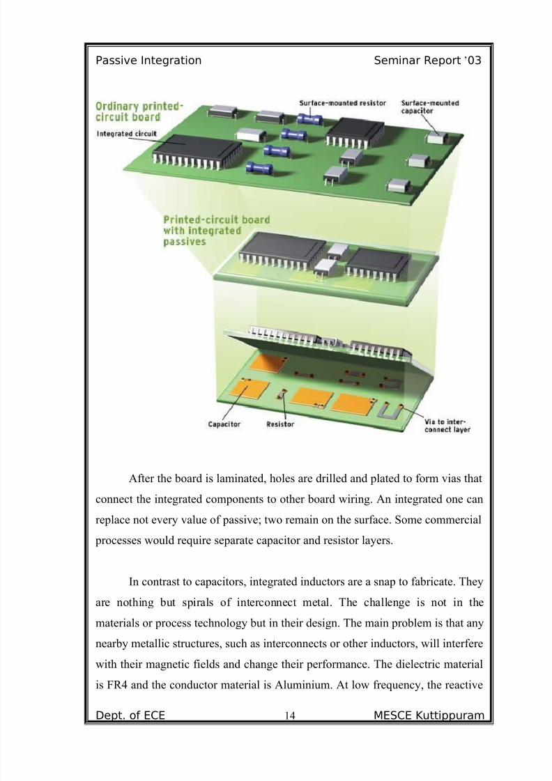
Size matters
Integrating passives can drastically reduce the size of an ordinary circuit
board [top]. Here, four capacitors and six resistors have been removed from the
surface and put into an extra layer of circuit board [bottom]. Resistors are copper
connection points bridged by a resistive film, and capacitors are conductive
plates separated by a thin film of dielectric material.
Dept. of ECE MESCE Kuttippuram13
7/28/2019 Passive Integration
http://slidepdf.com/reader/full/passive-integration 14/26
Passive Integration Seminar Report ’03
After the board is laminated, holes are drilled and plated to form vias that
connect the integrated components to other board wiring. An integrated one can
replace not every value of passive; two remain on the surface. Some commercial
processes would require separate capacitor and resistor layers.
In contrast to capacitors, integrated inductors are a snap to fabricate. They
are nothing but spirals of interconnect metal. The challenge is not in the
materials or process technology but in their design. The main problem is that any
nearby metallic structures, such as interconnects or other inductors, will interfere
with their magnetic fields and change their performance. The dielectric material
is FR4 and the conductor material is Aluminium. At low frequency, the reactive
Dept. of ECE MESCE Kuttippuram14

7/28/2019 Passive Integration
http://slidepdf.com/reader/full/passive-integration 15/26
Passive Integration Seminar Report ’03
inductance is smaller than the series resistance, therefore, the resistance
dominates the impedence. The resonant frequency is determined by the parasitic
capacitance of the inductors.
Inductors are angled away from each other to avoid crosstalk in this low-
pass filter that fits between the layers of a circuit board. Designed by one of the
authors, and built by Integral Wave Technologies for NASA's Langley Research
Center, the thickest part of this filter is less than 6 µm. Capacitors are made from
a thin-film oxide, inductors from copper.
A Very Flat Filter
Dept. of ECE MESCE Kuttippuram15

7/28/2019 Passive Integration
http://slidepdf.com/reader/full/passive-integration 16/26

7/28/2019 Passive Integration
http://slidepdf.com/reader/full/passive-integration 17/26
Passive Integration Seminar Report ’03
The blem of infrastructure is the usual chicken-and-egg story. When
plotted against time, technology adoption typically takes the form of an S curve,
meaning prothat little happens at first but eventually everyone gets on board.We
are at the bottom of the curve now, but there is evidence that adoption is
increasing. About a dozen products for integrating capacitors are on the market
now, which is double the number a year ago. Still, board manufacturers may be
squeamish until there are enough vendors in the business to guarantee a second
source for their materials and processes should their first choice fail.
The other inhibitors are:
• Need to demonstrate the technical viability of integral
substrates,including materials,processes,design and test system.
• Need to demonstrate the value or economic justification for
substituting discrete capacitor and resistors with integral
technology.
• Potential delay to the product development cycle. These passives
are usually designed in the final stages of a product.The economic
impact of a product delay could easily out way any cost saving in
size reduction or conversion costs.
• Integral passives reduce engineering and manufacturing
flexibility.The ability to apply engineering changes to an integral
substrate without delaying the schedule is critical.
• Qualification-most of the processes, materials, vendors and
products in this space are not qualified.
• Lack of availability from multiple suppliers.
• Industry standards are required to capture the true market potential
for this technology.
Dept. of ECE MESCE Kuttippuram17

7/28/2019 Passive Integration
http://slidepdf.com/reader/full/passive-integration 18/26
Passive Integration Seminar Report ’03
DECOUPLING
Decoupling may be considered as a killer application of integrated
passives. Decoupling is used in high-frequency digital logic circuits, such as in
the motherboards of laptop computers. These circuits place severe demands on
power-distribution systems to supply stable, noise-free power during the clock-
driven simultaneous switching of millions of transistor gates.
Decoupling capacitors help supply these large current surges, ramping asfast as 500 A/ns, to high-power microprocessor and logic ICs during the
switching portions of clock cycles. This technique ensures that the logic voltage
levels do not drop unacceptably as a result of the high current demands on the
power supply, which may be many centimeters away and connected by
unavoidably resistive and inductive conductor planes.Between cycles of current
demand, the power-distribution system recharges these capacitors in preparation
for the next switching cycle. With ever-increasing clock speeds, decreasing
power supply voltage, and increasing current demand, designers are finding it
harder and harder to supply low-impedance, noise-free power to ICs. The main
problem is that decoupling capacitors can't deliver charge quickly, because of
their intrinsic inductance.
Decoupling is an obvious first application for integrated capacitors for
two reasons: they won't take up valuable real estate near the power-hungry
microprocessor, and their electrical performance is superior in this application
by virtue of their extremely low parasitic inductance. Especially on digital
circuit boards, surface-mounted capacitors surround the big ICs, often on both
sides of the board. Since the speed of the system is often limited by memory
access times, eliminating the capacitors from the surface and moving memory
closer to the microprocessors would result in a smaller and faster system.
Dept. of ECE MESCE Kuttippuram18
7/28/2019 Passive Integration
http://slidepdf.com/reader/full/passive-integration 19/26
Passive Integration Seminar Report ’03
Though special discrete capacitors are being built with fairly low
inductance, none of them can compare with an integrated parallel-plate capacitor
using a thin dielectric located between the power and ground planes (conductor
coated layers of the board dedicated to either the ground or power supply). For
example, thin-film devices that we built on flex at the University of Arkansas
(Fayetteville) and Xanodics deliver several hundred nanofarads with less than 3
picohenrys of inductance and a trifling 10 milliohms of resistance. In
comparison, a typical surface-mounted capacitor would have several hundred
picohenrys of inductance. Integrated decoupling will likely first appear not in the
circuit board itself, but in the small piece of substrate included in the so called
ball-grid-array packaging of high-performance microprocessors.Putting the
capacitance layer within the package avoids the intervening inductance of the
package-to-board connection.
Dept. of ECE MESCE Kuttippuram19

7/28/2019 Passive Integration
http://slidepdf.com/reader/full/passive-integration 20/26
Passive Integration Seminar Report ’03
THE INTERMEDIATE STEP
Before true integrated passives take hold, widespread use of passive
arrays can be seen, in which multiple similar components (capacitors, say) are
formed on the surface of a substrate and packaged into a single surface mounted
device like an IC. We'll also see more passive networks, which combine
different kinds of passives in one package. These networks include devices
internally connected to form simple circuits such as filters, terminators, or
voltage dividers. In either case, one mounting operation replaces many and the
overall footprint of the circuit is much smaller. These arrays and networks are a
middle ground—not fully discrete but not fully integrated within a circuit board.
They bring some of the advantages of full integration such as a reduced number
of placement operations, fewer solder joints, and less board space. Many
configurations of arrays and networks are now available in quantity from
California Micro Devices, AVX, and other companies, and custom arrangements
are also possible. Devices from these companies are typically fabricated on a
silicon or other substrate using tried-and-true chip-making processes so the
yields are high and the prices reasonable.
The technique raises some interesting possibilities. If ICs or other active
devices are mounted atop a passive network, they may form so-called functional
modules, such as Bluetooth or GPS subsystems. For example, a GPS module
would include passives and antennas integrated on a substrate and one or more
ICs bound to it, all in a single chip-scale package. The manufacturer would not
have to worry about learning to design and manufacture GPS systems and could
also easily upgrade or switch vendors.
Dept. of ECE MESCE Kuttippuram20

7/28/2019 Passive Integration
http://slidepdf.com/reader/full/passive-integration 21/26
Passive Integration Seminar Report ’03
FUTURE SCOPE
Less than 5 percent of the trillion-plus passive devices mounted on FR4
and flex boards this year will be surface-mounted passive arrays and passive
networks, and hardly any passives will be fully integrated into the circuit board.
The circuit board business, in the United States, at least, is largely a
contract industry, with much of it removed from the designers of circuits and
equipment makers. This gulf makes board makers a bit conservative and slow to
change relative to, say, the chip industry, where all aspects of development,
design, and manufacture are often in the same company. Still, integrated resistor
and capacitor layers are starting to become available from reputable suppliers
and a few consumer products are showing up with at least some of the passives
integrated, and these should lead the way for significant market penetration in
the near future. It is hard to say when, if ever, will more than half the passives be
integrated. The microelectronics industry is full of cautionary tales. But some
new manufacturing technologies do prove their economic viability and become
industry standards, such as surface mounting.
Whether or not passive integration becomes an industry standard will
depend on its economic viability. Certainly, it is viable for decoupling and, in
fact, may be the only way to handle the future generations of high-power, high-
frequency microprocessors. For discrete replacement in general, though, the best
processes and materials are still being identified. If we find suitable
technologies, then passive integration will probably show a long, steady climb in
use the way surface mounting supplanted through-hole mounting in the 1980s.
As the infrastructure, supply chain, and industry acceptance grow
Dept. of ECE MESCE Kuttippuram21
7/28/2019 Passive Integration
http://slidepdf.com/reader/full/passive-integration 22/26
Passive Integration Seminar Report ’03
simultaneously, eventually integration will gain some significant fraction of the
total market and put passives in their place: hidden, ubiquitous, and cheap.
CONCLUSION
The need for increased product miniaturization and increased product
function will eventually drive the electronic product to increase their use of
integral passive components.Embedded passives offer increased component
density beyond the physical capability of discrete-like devices.They also offer
high product reliability and eventually lower overall system costs via decreased
conversion costs.
Although severely lagging behind developments in active components,
passive component integration is allowing the development of an assortment of
new product offerings. Some of these items have been possible for several years,
but lack of widespread customer acceptance and high costs have slowed their
introduction into the general marketplace. Some items are yet to be developed.
For example, because several manufacturers can perform both thick- and thin-
film manufacturing, hybrid components combining both technologies may be
forthcoming. Passive component integration is and will continue to be an
important contribution in the development of increasingly smaller medical
electronics.
Resistors, inductors, and capacitors are disappearing from view,
integrated into the circuit board itself. Passive integration may be the only way
to handle the future generations of high-power, high-frequency microprocessors.
Dept. of ECE MESCE Kuttippuram22
7/28/2019 Passive Integration
http://slidepdf.com/reader/full/passive-integration 23/26
Passive Integration Seminar Report ’03
REFERENCES
Books:
1. IEEE SPECTRUM Journal,July 2003
2. Integrated Passive Component technology-IEEE/WILEY Press
3. IMAPS Advanced Packaging Materials Processes, March 2001
Websites:
1. www.spectrum.ieee.org
2. www.identrus.com/Baltimore.pdf
3. http:/www.pemuk.com
4. www.ewh.ieee.org/mm/cpmt/kim00/emps.pdf
Dept. of ECE MESCE Kuttippuram23
7/28/2019 Passive Integration
http://slidepdf.com/reader/full/passive-integration 24/26
Passive Integration Seminar Report ’03
CONTENTS
1. INTRODUCTION
2. NEED FOR PASSIVE INTEGRATION
3. COMPARISON BETWEEN EMBEDDED
AND DISCRETE PASSIVES
4. INTEGRATED PASSIVE TECHNOLOGY
5. BARRIERS TO PASSIVE INTEGRATION
6. DECOUPLING
7. THE INTERMEDIATE STEP
8. FUTURE SCOPE
9. CONCLUSION
10. REFERENCES
Dept. of ECE MESCE Kuttippuram24

7/28/2019 Passive Integration
http://slidepdf.com/reader/full/passive-integration 25/26
Passive Integration Seminar Report ’03
ABSTRACT
Miniaturization has been a key contributor to advances in electronic
technology. Many electronics applications have serious space considerations that
are pressuring manufacturers to reduce component size. Much of the motivation
for this Certainly, miniaturization has been made possible mostly through
remarkable breakthroughs in reducing the size of active components. But as
integrated circuits get smaller and more complex, there is an increasing need to
also reduce the space required for the supporting passive components.
Passive integration suggests that if the passives were so small and flat,
then they could be inserted between layers of the circuit board itself, rather than
taking space on top of it. The integrated passives would be a part of the circuit
board itself, formed when the board was, so odds are good that their overall cost
could eventually be less than what manufacturers pay today to buy and solder on
discrete devices. Advantages of this technology point to a potentially huge shift
for the electronics industry. Passive component integration is and will continue
to be an important contribution in the development of electronic technology.
Dept. of ECE MESCE Kuttippuram25

7/28/2019 Passive Integration
http://slidepdf.com/reader/full/passive-integration 26/26