pc sdram registered dimm design support document
TRANSCRIPT

PC SDRAM Registered DIMM Design Support Document
Oct. 98 Page 1 of 61 Revision 1.2
PC SDRAM Registered DIMM Design SupportDocument
REVISION 1.2
October 1998
The information in this document is subject to change.

PC SDRAM Registered DIMM Design Support Document
Oct. 98 Page 2 of 61 Revision 1.2
THIS DOCUMENT IS PROVIDED "AS IS" WITH NO WARRANTIES WHATSOEVER,INCLUDING ANY WARRANTY OF MERCHANTABILITY, NONINFRINGEMENT,FITNESS FOR ANY PARTICULAR PURPOSE, OR ANY WARRANTY OTHERWISEARISING OUT OF ANY PROPOSAL, SPECIFICATION OR SAMPLE. Intel disclaims allliability, including liability for infringement of any proprietary rights, relating to use ofinformation in this document. No license, express or implied, by estoppel or otherwise,to any intellectual property rights is granted herein.
* *Third-party brands and names are the property of their respective owners.
Copyright Intel Corporation, 1997, 1998

PC SDRAM Registered DIMM Design Support Document
Oct. 98 Page 3 of 61 Revision 1.2
TABLE OF CONTENTS
1 LIST OF TABLES.................................................................................................................................. 42 LIST OF FIGURES ................................................................................................................................ 53 REVISION HISTORY ........................................................................................................................... 64 Introduction............................................................................................................................................. 7
4.1 Related Documents 74.2 DIMM Configurations 8
5 Environmental Requirements.................................................................................................................. 85.1 Safety - UL Rating 8
6 Mechanical Design.................................................................................................................................. 97 Module Pins .......................................................................................................................................... 178 SDRAM DIMM Block Diagrams ......................................................................................................... 199 DIMM Post-Register Timing ................................................................................................................ 26
9.1 Registered Mode 269.2 Buffered Mode 27
10 DIMM PCB Layout and Signal Routing........................................................................................... 2810.1 Printed Circuit Board 2810.2 DIMM PCB and final assembly labeling requirements 30
10.2.1 DIMM Naming Convention 3010.2.2 Printed Circuit Board Labeling 30
10.3 Component Types and Placement 3110.4 Signal Groups 3210.5 Signal Topology and Length Restrictions 32
10.5.1 Routing Rules 3210.5.2 Topology Diagram Explanation and Examples 3310.5.3 Topology for Clock: CK[3:0] 3510.5.4 Topology for Data: DQ[63:0] & CB[7:0] 39
11 SDRAM Component Specifications ................................................................................................. 5012 EEPROM Component Specifications ............................................................................................... 5113 Register Component Specifications .................................................................................................. 5214 PLL Component Specifications ........................................................................................................ 58

PC SDRAM Registered DIMM Design Support Document
Oct. 98 Page 4 of 61 Revision 1.2
1 LIST OF TABLES
TABLE 1: RELATED DOCUMENTS 7TABLE 2: SDRAM MODULE CONFIGURATIONS 8TABLE 3: DIMM ENVIRONMENTAL REQUIREMENTS 8TABLE 4: DIMM DIMENSIONS AND TOLERANCES 9TABLE 5: REGISTERED DIMM MODULE PINOUT 17TABLE 6: PIN DESCRIPTIONS 18TABLE 7: REGISTERED / BUFFERED MODE OPERATION 18TABLE 8: EXAMPLE OF REGISTERED MODE TIMING 26TABLE 9: EXAMPLE OF BUFFERED MODE TIMING 27TABLE 10: PCB CALCULATED PARAMETERS 28TABLE 11: SIGNAL TOPOLOGY CATEGORIES 32TABLE 12: TRACE LENGTH AND COMPONENT VALUE TABLE FOR DIMM CONNECTOR TO
PLL CLOCK-IN TOPOLOGIES 37TABLE 13: TRACE LENGTH TABLE FOR CLOCK TOPOLOGIES 38TABLE 14: TRACE LENGTH TABLE FOR DATA TOPOLOGIES 39TABLE 15: TRACE LENGTH TABLE FOR DATA MASK TOPOLOGIES (2/4 LOADS) 40TABLE 16: TRACE LENGTH TABLE FOR DATA MASK TOPOLOGIES (1/2/3/6 LOADS) 41TABLE 17: TRACE LENGTH TABLE FOR CHIP SELECT TOPOLOGIES (S0, S1) 42TABLE 18: TRACE LENGTH FOR CHIP SELECT TOPOLOGIES (S0, S1, S2, S3) 43TABLE 19: TRACE LENGTH TABLE FOR ADDRESS AND CONTROL SIGNALS 44TABLE 20: TRACE LENGTH TABLE FOR ADDRESS AND CONTROL SIGNALS CONTD. 44TABLE 21: TRACE LENGTH TABLES FOR CLOCK ENABLE TOPOLOGIES 45TABLE 22: TRACE LENGTH TABLES FOR CLOCK ENABLE TOPOLOGIES 46TABLE 23: TRACE LENGTH TABLE FOR ADDRESS AND CONTROL SIGNALS 47TABLE 24: RESISTANCE VALUES IN THE ADDRESS AND CONTROL SIGNAL TOPOLOGIES 48TABLE 25: TRACE LENGTH TABLE FOR WRITE ENABLE 49TABLE 26: STACKED COMPONENT PIN CAPACITANCE 50TABLE 27: DIMM REGISTER USE 52TABLE 28: REGISTER SPECIFICATION PARAMETRICS 52TABLE 29: 16835 I-V DATA 55TABLE 30: 162835 I-V DATA 57TABLE 31: PLL COMPONENT SPECIFICATIONS 58TABLE 32: DIMM PLL USE 59TABLE 33: PLL OUTPUT I-V DATA 61

PC SDRAM Registered DIMM Design Support Document
Oct. 98 Page 5 of 61 Revision 1.2
2 LIST OF FIGURES
FIGURE 1: DIMM MECHANICAL DRAWING (1 OF 5) 12FIGURE 2: DIMM MECHANICAL DRAWING (2 OF 5) 13FIGURE 3: DIMM MECHANICAL DRAWING (3 OF 5) 14FIGURE 4: DIMM MECHANICAL DRAWING (4 OF 5) 15FIGURE 5: DIMM MECHANICAL DRAWING (5 OF 5) 16FIGURE 6: 64MBYTE 72-BIT ECC SDRAM DIMM BLOCK DIAGRAM (1 ROW X8 SDRAMS) 19FIGURE 7: 64MBYTE 72-BIT ECC SDRAM DIMM BLOCK DIAGRAM (1 ROW X8 SDRAMS) 20FIGURE 8: 72-BIT ECC UNSTACKED SDRAM DIMM BLOCK DIAGRAM (1 ROW X4 SDRAMS) 21FIGURE 9: 72-BIT ECC STACKED SDRAM DIMM BLOCK DIAGRAM (2 ROWS X4 SDRAMS) 22FIGURE 10: REGISTER WIRING ON 64MBYTE DIMMS 23FIGURE 11: REGISTER WIRING FOR DIMM USING 18 SDRAMS 23FIGURE 12: REGISTER WIRING FOR STACKED DIMM USING 36 SDRAMS 24FIGURE 13: STACKED SDRAM COMPONENT PINOUT 24FIGURE 14: CLOCK LOADING TABLE & WIRING DIAGRAM 25FIGURE 15: EXAMPLE 6-LAYER STACKUP FOR 6 MIL TRACES 28FIGURE 16: EXAMPLE 6-LAYER STACKUP FOR 4 MIL TRACES 29FIGURE 17: EXAMPLE 256MBYTE COMPONENT PLACEMENT 31FIGURE 18: EXAMPLE TOPOLOGY 34FIGURE 19: DIMM CLOCK REFERENCE AND TIMING (NOT TO SCALE) 36FIGURE 20: SIGNAL ROUTING TOPOLOGIES FOR CLOCKS PRE-PLL 37FIGURE 21: SIGNAL ROUTING TOPOLOGIES FOR CLOCKS POST-PLL 38FIGURE 22: SIGNAL ROUTING TOPOLOGIES FOR DATA 39FIGURE 23: SIGNAL ROUTING TOPOLOGIES FOR DATA MASK (1/2/4 LOADS) 40FIGURE 24: SIGNAL ROUTING TOPOLOGIES FOR DATA MASK (3/6 LOADS) 41FIGURE 25: SIGNAL ROUTING TOPOLOGIES FOR CHIP SELECT (64MB) 42FIGURE 26: SIGNAL ROUTING TOPOLOGIES FOR CHIP SELECT (> 64MB DIMM) 43FIGURE 27: SIGNAL ROUTING TOPOLOGIES FOR CLOCK ENABLE (64MB) 44FIGURE 28: SIGNAL ROUTING TOPOLOGIES FOR CLOCK ENABLE (UNSTACKED DIMM) 45FIGURE 29: SIGNAL ROUTING TOPOLOGIES FOR CLOCK ENABLE (STACKED DIMM) 46FIGURE 30: SIGNAL ROUTING TOPOLOGIES FOR ADDRESS AND CONTROL SIGNALS 47FIGURE 31: SIGNAL ROUTING TOPOLOGIES FOR WRITE ENABLE (STACKED DIMM) 49FIGURE 32: I-V CHARACTERISTICS FOR 16835 REGISTER OUTPUT – PULL DOWN 54FIGURE 33: I-V CHARACTERISTICS FOR 16835 REGISTER OUTPUT – PULL UP 54FIGURE 34: I-V CHARACTERISTICS FOR 162835 REGISTER OUTPUT – PULL DOWN 56FIGURE 35: I-V CHARACTERISTICS FOR 162835 REGISTER OUTPUT – PULL UP 56FIGURE 36: I-V CHARACTERISTICS FOR PLL OUTPUT – PULL UP 60FIGURE 37: I-V CHARACTERISTICS FOR PLL OUTPUT – PULL DOWN 60

PC SDRAM Registered DIMM Design Support Document
Oct. 98 Page 6 of 61 Revision 1.2
3 REVISION HISTORY
Revision 0.8: December 1997• Added post register timing information• Add PLL critical specifications• Add register critical specifications• Corrected register part numbers• Updated post register timing information• Added new 256MB Topology information• Added preliminary information on the 64MB DIMM without the PLL• Added preliminary information on adapting the spec for 512MB DIMM
Revision 1.0: February 1998• Updated Introduction section• Updated information for the 64MB DIMM without the PLL• Updated all topology and component value tables• Corrected PLL part numbers• Modified PLL component requirements to support SSC synthesizers• Added VI curves for the Register and PLL
Revision 1.1: August 1998• Updated Introduction section• Updated information for the 512MB and 1024MB DIMM designs• Added Buffered mode documentation• Renumbered Chapters• Updated Chapter 10:
n clock distribution tuning methodologyn register offset timingn New clock topologies for 128MB designn New C1 spec capacitance, and C3 recommended tuning capacitance
• Updated Chapter 13:n removed manufacturer references for registersn added detailed register specificationsn modified and consolidated IBIS I/V curves
• Updated Chapter 14:n removed manufacturer references for PLL componentsn added detailed PLL specificationsn modified IBIS I/V curves to reflect min-max I/V limits
Revision 1.2: October 1998• Added Test conditions in Register and PLL specifications• Modified Environmental Requirements• Added UL Requirements• Updated stacked SDRAM component pin capacitance values

PC SDRAM Registered DIMM Design Support Document
Oct. 98 Page 7 of 61 Revision 1.2
4 Introduction
This document defines the electrical and mechanical requirements for the 168-pin, 3.3 volt, 72-bit wide,PC SDRAM Registered DIMM. It is intended to serve as a guide to the DIMM designer, as well as thesystem integrator of the DIMM. This DIMM supports two modes of operation: (a) Buffered mode at 66*MHz or (b) Registered mode at 100 MHz. The PC SDRAM Registered DIMM is intended for use as mainmemory when installed on personal computer motherboards.
*Note: all references to 66 MHz imply 66.67 MHz (15ns clock period).
A reference design example is presented in this document. The reference design is intended to provide aninitial basis for a registered DIMM design. Modifications to this reference design may be required to meetall system timing, signal integrity and thermal requirements for 66 MHz or 100 MHz support. Allregistered DIMM implementations must use simulations and lab verification to insure proper timingrequirements and signal integrity in the design.
The 256MB, 512MB and 1GB registered DIMMs are implemented using a stacked SDRAM packageapproach. Other SDRAM packaging implementations may be used.
4.1 Related Documents
Table 1: Related Documents
Title RevIntel PC SDRAM Specification Latest RevisionIntel PC SDRAM SPD Data Structure Specification Latest Revision

PC SDRAM Registered DIMM Design Support Document
Oct. 98 Page 8 of 61 Revision 1.2
4.2 DIMM Configurations
SDRAM DIMM configurations are defined in the following table:
Table 2: SDRAM Module Configurations
Config # DIMMCapacity
DIMMOrganization
SDRAMdensity
SDRAMOrganization
# ofSDRAMs
# Rows ofSDRAM
# Banks inSDRAM
# Address bitsrow/bank/col
1 64 MB 8M X 72 64Mbit 8M X 8 9 1 4 12/2/9
2 128 MB 16M X 72 64Mbit 16M X 4 18 1 4 12/2/10
3 256 MB 32M X 72 64Mbit 16M X 4 36 2 4 12/2/10
4 256MB 32M X 72 128Mbit 32M X 4 18 1 4 12/2/11
5 512MB 64M X 72 128Mbit 32M x 4 36 2 4 12/2/11
6 512MB 64M X 72 256Mbit 64M x 4 18 1 4 13/2/11
7 1024 MB 128M X 72 256Mbit 64M x 4 36 2 4 13/2/11
5 Environmental Requirements
The Registered SDRAM DIMM shall be designed to operate within a personal computer cabinet in anoffice environment with limited capacity for heating and air conditioning. The temperature and humiditylimits are listed below.
Table 3: DIMM Environmental Requirements
Parameter RangeOperating Temperature System Operating Conditions1:
0-55 deg C ambient 500 MB/sec sustained READ 0 LFM airflow
Operating Humidity 10% to 90% relative humidityStorage Temperature -50 oC to + 100 oCStorage Humidity 5% to 95% without condensationAltitude (operating & storage) -500 ft. to 10,000 ft.
1 Actual system operating conditions may vary, depending upon airflow, maximum allowedmemory bandwidth, and ambient temperature.
5.1 Safety - UL Rating Printed circuit board to have a flammability rating of 94V-0. Markings to include UL tractability requirements per UL Recognized Component Directory.

PC SDRAM Registered DIMM Design Support Document
Oct. 98 Page 9 of 61 Revision 1.2
6 Mechanical Design
The following table and mechanical drawings give the specific dimensions and tolerances for a 168-pinRegistered DIMM.
Table 4: DIMM Dimensions and Tolerances
DIMM Dimensions and TolerancesSYMBOL DEFINITION MIN NOM MAX NOTESA Overall module height
measured from Datum -B-.38.12 mm 43.18 mm Nominal is 38.10 mm. (1.5”).
Max is 43.18 (1.7”).
A1 The distance from Datum -B-to the centerline of the PWBalignment holes.
3.00 mm BASICThese holes are not used bythe next level of assembly.The dimensions are suppliedfor information only. If theholes are used inmanufacturing they should betightly toleranced. Therecommended positionaltolerance is 0.10 mm.
A2 The distance from Datum -B-to the centerline of the latchholes.
17.80 mm BASIC
A3The distance from Datum -B-to the lower edge of theComponent Area.
20.80 mmThis distance applies to theComponent Area in the latchhole area.
A4The distance from Datum -B-to the lower edge of theComponent Area on the frontside of the PWB.
4.00 mm
A5The distance from Datum -B-to the lower edge of theComponent Area on the backside of the PWB.
4.00 mm
A6The distance from Datum -B-to the leading edge of thecontact.
0.05 mm 0.35 mmThe minimum distanceprevents contact edge burrs.
BThe width of the platedinput/output contact measuredat the lateral midpoint of thecontact.
0.95 mm 1.00 mm 1.05 mm
D1 The overall length of thePWB.
133.22 mm 133.37 mm 133.52 mm
D2 The longitudinal distancebetween the PWB machiningalignment hole centers.
126.20 mm 127.35 128.50 mmThese holes are optional andmay or may not be present. Ifthey are present, they must belocated as defined.

PC SDRAM Registered DIMM Design Support Document
Oct. 98 Page 10 of 61 Revision 1.2
DIMM Dimensions and TolerancesSYMBOL DEFINITION MIN NOM MAX NOTESE The pitch or distance between
centerlines of the contacts1.27 mm BASIC
e1The distance between thecenterlines of Contact 1 and84.
115.57 mm
e2The distance between thecenterlines of Contact 85 and168.
115.57 mm
e3The distance between thecenterlines of Contact 1 andthe contact located at theimmediate left of the left keyzone when viewing contact 1side.
11.43 mm The distance between thecenterlines of contact 1 and10.
e4The distance between thecenterlines of the contact at theimmediate right of the left keyzone and the contact at theimmediate left of the centerkey zone when viewingcontact 1 side.
36.83 mm The distance between thecenterlines of contact 11 and40.
e5The distance between thecenterlines of the contactlocated at the immediate rightof the center key zone andcontact 84.
54.61 mm The distance between thecenterlines of contact 41 and84.
H The diameter of the PWBmachined alignment holes.
2.90 mm 3.00 mm 3.10 mm The machined alignmentholes are optional.
LThe distance from Datum -B-to the top edge of the platedcontact.
2.30 mm 2.50 mm 2.70 mm
N The total number of contacts. 168
TThe thickness of the PCBincluding the contactmetalization and plating.
1.17 mm 1.27 mm 1.37 mm
T1The overall thickness of thePWB with the componentsmounted. The overallthickness is measured from thehighest component on the frontside to the highest componenton the backside.
8.13 mm
Aaa The positional tolerance forthe overall body length D1.
aaa = 0.15 mm @ Maximum Material Condition
BbbThe straightness tolerance forthe card thickness includingthe metalized contacts. Thiscallout applies to the zonedefined by A4, A5 and D1.
0.40 mm bbb = 0.3% x D1 rounded toa two decimal place hardmetric value.
The positional tolerance for

PC SDRAM Registered DIMM Design Support Document
Oct. 98 Page 11 of 61 Revision 1.2
DIMM Dimensions and TolerancesSYMBOL DEFINITION MIN NOM MAX NOTESCcc the pattern of contacts with
regard to primary Datum -A-.ccc = 0.10 mm @ Least Material Condition
DddThe positional tolerance forthe individual contact width bwith regard to the theoreticalcenterline of the contactdefined by basic dimension e.
ddd = 0.05 mm @ Least Material Condition

PC SDRAM Registered DIMM Design Support Document
Oct. 98 Page 12 of 61 Revision 1.2
COMPONENT AREA(FRONT)
(DATUM -A-)
CONTACT 1
CONTACT 84
CENTER KEY ZONELEFT KEY ZONE
A
COMPONENT AREA(BACK)
CONTACT 85 CONTACT 168
D1
A12X
1
CONTACT 1 ID
A22X
A32X
- B -
3.00 TYP 3.00 TYP44
M SABCaaa
2XSEE DETAIL BDETAIL C
DETAIL A
D2 / 2
D2
M MA BC0.102X H
OPTIONAL HOLES
(DATUM -A-)
DETAIL D
Figure 1: DIMM Mechanical Drawing (1 of 5)

PC SDRAM Registered DIMM Design Support Document
Oct. 98 Page 13 of 61 Revision 1.2
(DATUM -A-)
CENTER KEY ZONELEFT KEY ZONE
1
(DATUM -A-)
FRONT AND BACK CONTACTCENTERLINES ARE COINCIDENT
e2
e1
e5e4e3
6.35 6.35
3.175
Figure 2: DIMM Mechanical Drawing (2 of 5)

PC SDRAM Registered DIMM Design Support Document
Oct. 98 Page 14 of 61 Revision 1.2
T
T1
END VIEW
Note: No chamferon leading edge
A4 A5
- C -
5 9
5
6Mbbb
L
162 X e
168 X b 10
8A6
DETAIL A DETAIL B
L SABCcccL Bddd
(3.00)
4.00 + 0.10
FULLRADIUS
M M BAC0.10
Figure 3: DIMM Mechanical Drawing (3 of 5)

PC SDRAM Registered DIMM Design Support Document
Oct. 98 Page 15 of 61 Revision 1.2
DETAIL C - CENTER KEY ZONE
(DATUM -A-)
3.175
1.00
FULL R
2.00 + 0.10
3.003.25
L SABC0.10
1.00
FULL R
3.25
DETAIL D - LEFT KEY ZONE
3.00
2.00 + 0.10L SABC0.10
4.175
KEYWAYZONE
KEYWAYZONE
CONTACT 10
CONTACT 11
CONTACT 41
CONTACT 40
Figure 4: DIMM Mechanical Drawing (4 of 5)

PC SDRAM Registered DIMM Design Support Document
Oct. 98 Page 16 of 61 Revision 1.2
1 ALL DIMENSIONING AND TOLERANCING CONFORM TO ANSI Y14.5M-1994.
NOTES
2 TOLERANCES ON ALL DIMENSIONS +/- 0.13 UNLESS OTHERWISE SPECIFIED.
3 ALL DIMENSIONS ARE IN MILLIMETERS.
4 3.00 mm TYPICAL APPLIES TO BOTH 4.00 mm WIDE NOTCH LENGTH AND COMPONENT KEEPOUT AREA.
5 DIMENSION APPLICABLE WHEN COMPONENTS MOUNTED ON BOTH SIDES.
6 CARD THICKNESS APPLIES ACROSS THE CONTACTS AND INCLUDES PLATING AND/OR METALIZATION. STRAIGHTNESS CALLOUT APPLIES TO ZONE DEFINED BY A4, A5, AND D1.
7 N IS THE TOTAL NUMBER OF CIRCUIT CONTACTS (PINS, LEADS, TABS OR PADS).
8 LEADING EDGE OF CONTACT ZONE SHALL BE FREE OF BURRS AND EXTERNAL TIE BARS.
9 THE MAXIMUM THICKNESS OVERALL SHALL NOT EXCEED 8.13 mm.
APPLICATION NOTES:10 PLATING FOR CONTACT PADS: GOLD PLATING 0.75 MICROMETER MINIMUM OVER NI PLATING 2 MICROMETERS MINIMUM.
11 FOR OPTIMUM PERFORMANCE, IT IS RECOMMENDED THAT THE TIEBAR BE OFFSET FROM THE CENTERLINE OF THE PAD. ALSO, THE TIEBAR MAY BE AN INTERNAL LAYER, SO THE REMNANT CANNOT CAUSE CONTACT DAMAGE.
Figure 5: DIMM Mechanical Drawing (5 of 5)

PC SDRAM Registered DIMM Design Support Document
Oct. 98 Page 17 of 61 Revision 1.2
7 Module PinsThe following table provides the 168-pin 72-bit registered DIMM module connector pinout. Note that theeight error detection and correction bits CB(0:7) are actually NC for the 64-bit pinout.
Table 5: Registered DIMM Module Pinout
Pin# SignalName
Pin# SignalName
Pin# SignalName
Pin# SignalName
1 Vss 43 Vss 85 Vss 127 Vss2 DQ0 44 DU 86 DQ32 128 CKE03 DQ1 45 /S2 87 DQ33 129 /S34 DQ2 46 DQMB2 88 DQ34 130 DQMB65 DQ3 47 DQMB3 89 DQ35 131 DQMB76 Vcc 48 DU 90 Vcc 132 A137 DQ4 49 Vcc 91 DQ36 133 Vcc8 DQ5 50 NC 92 DQ37 134 NC9 DQ6 51 NC 93 DQ38 135 NC
10 DQ7 52 CB2 94 DQ39 136 CB611 DQ8 53 CB3 95 DQ40 137 CB712 Vss 54 Vss 96 Vss 138 Vss13 DQ9 55 DQ16 97 DQ41 139 DQ4814 DQ10 56 DQ17 98 DQ42 140 DQ4915 DQ11 57 DQ18 99 DQ43 141 DQ5016 DQ12 58 DQ19 100 DQ44 142 DQ5117 DQ13 59 Vcc 101 DQ45 143 Vcc18 Vcc 60 DQ20 102 Vcc 144 DQ5219 DQ14 61 NC 103 DQ46 145 NC20 DQ15 62 Vref, NC 104 DQ47 146 Vref, NC21 CB0 63 CKE1 105 CB4 147 REGE22 CB1 64 Vss 106 CB5 148 Vss23 Vss 65 DQ21 107 Vss 149 DQ5324 NC 66 DQ22 108 NC 150 DQ5425 NC 67 DQ23 109 NC 151 DQ5526 Vcc 68 Vss 110 Vcc 152 Vss27 /WE 69 DQ24 111 /CAS 153 DQ5628 DQMB0 70 DQ25 112 DQMB4 154 DQ5729 DQMB1 71 DQ26 113 DQMB5 155 DQ5830 /S0 72 DQ27 114 /S1 156 DQ5931 DU 73 Vcc 115 /RAS 157 Vcc32 Vss 74 DQ28 116 Vss 158 DQ6033 A0 75 DQ29 117 A1 159 DQ6134 A2 76 DQ30 118 A3 160 DQ6235 A4 77 DQ31 119 A5 161 DQ6336 A6 78 Vss 120 A7 162 Vss37 A8 79 CK2 121 A9 163 CK338 A10 (AP) 80 NC 122 BA0 164 NC39 BA1 81 WP 123 A11 165 SA040 Vcc 82 SDA 124 Vcc 166 SA141 Vcc 83 SCL 125 CK1 167 SA242 CK0 84 Vcc 126 A12 168 Vcc
Note: NC = Not Connected; DU = Don’t Use
Note: DIMM signals BA0, BA1, A12 and above may be connected to the A12, A13, A14 address lines andabove respectively on the motherboard.

PC SDRAM Registered DIMM Design Support Document
Oct. 98 Page 18 of 61 Revision 1.2
Table 6: Pin Descriptions
Pin Name Desription Pin Name DescriptionCK(0:3) Clock Inputs DQ(0:63) Data Input/OutputCKE(0:1) Clock Enables CB(0:7) ECC Data Input/Output/RAS Row Address Strobe DQMB(0:7) Data Mask/CAS Column Address Strobe Vcc Power (3.3V)/WE Write Enable Vss Ground/S(0:3) Chip Selects NC No ConnectA(0:9,11:13) Address Inputs SCL Serial Presence Detect Clock InputA10/AP Address Input/Autoprecharge SDA Serial Presence Detect Data
Input/OutputBA0-BA1 SDRAM Bank Address SA(0:2) Serial Presence Detect Address InputsREGE Register Enable WP Write Protect for SPD on DIMMDU Don’t Use - leave as NC NC No Connect
All pin functions are described in the “Intel PC SDRAM Specification” with the exception of REGE.
REGE is the Register Enable pin which permits the DIMM to operate in “buffered” mode (inputs re-drivenasynchronously) and “registered” mode (signals re-driven to SDRAMs when clock rises, and held validuntil next rising clock). To conform to this design guide, REGE must select the operating modeaccording to the following function table.
Table 7: Registered / Buffered Mode Operation
REGE Input DIMM ModeLow Buffered 1
High Registered
1 Note: All references to Buffered mode in this document are for operation at 66.67 MHz ( 15 nSperiod).

PC SDRAM Registered DIMM Design Support Document
Oct. 98 Page 19 of 61 Revision 1.2
8 SDRAM DIMM Block Diagrams
Figure 6: 64MByte 72-Bit ECC SDRAM DIMM Block Diagram (1 row x8 SDRAMs)
Non-PLL Implementation

PC SDRAM Registered DIMM Design Support Document
Oct. 98 Page 20 of 61 Revision 1.2
Figure 7: 64MByte 72-Bit ECC SDRAM DIMM Block Diagram (1 row x8 SDRAMs)
PLL Implementation

PC SDRAM Registered DIMM Design Support Document
Oct. 98 Page 21 of 61 Revision 1.2
Figure 8: 72-Bit ECC Unstacked SDRAM DIMM Block Diagram (1 row x4 SDRAMs)
128MB using 16Mx4 (64Mbit) SDRAMs256MB using 32Mx4 (128Mbit) SDRAMs512MB using 64Mx4 (256Mbit) SDRAMs
REGEPLL CLK
A0
Serial Presence Detect
A1 A2
SA0 SA1 SA2
SCL
SDA
VCC
VSS
D0 - D17
D0 - D17
CK0 *PLL
CK1, CK2, CK3 Terminated
RAS: SDRAMS D0 - D17CAS: SDRAMS D0 - D17CKE: SDRAMS D0 - D17
WE: SDRAMS D0 - D17
S0/S2DQMB0 to DQMB7BA0-BA1A0-A12RASCASCKE0WE
RS0/RS2RDQMB0 - RDQMB7
RRASRCASRCKE0RWE
REGISTER
RBA0 - RBA1RA0-RA12
BA0-BA1: SDRAMS D0-D17A0-A12: SDRAMS D0-D17
NOTE: DQ wiring may differ from that describedin this drawing; however DQ/DQMBrelationships must be maintained as shown.
VCC10k
#: Unless otherwise noted, resistor values are 10 OHMS.
WP47K
RS0
RDQMB2
RDQMB3
RDQMB1
DQ0DQ1DQ2DQ3
DQ4DQ5DQ6DQ7
DQ8DQ9DQ10DQ11
DQ12DQ13DQ14DQ15
DQ16DQ17DQ18DQ19
DQ20DQ21DQ22DQ23
DQ28DQ29DQ30DQ31
DQMI/O 0I/O 1I/O 2I/O 3
D0
DQMI/O 0I/O 1I/O 2I/O 3
DQMI/O 0I/O 1I/O 2I/O 3
DQMI/O 0I/O 1I/O 2I/O 3
DQMI/O 0I/O 1I/O 2I/O 3
DQMI/O 0I/O 1I/O 2I/O 3
DQMI/O 0I/O 1I/O 2I/O 3
RDQMB0
D1
D2
D3
D5
D6
D8
DQ24DQ25DQ26DQ27
DQMI/O 0I/O 1I/O 2I/O 3
D7
RDQMB6
RDQMB7
RDQMB5
DQ32DQ33DQ34DQ35
DQ36DQ37DQ38DQ39
DQ40DQ41DQ42DQ43
DQ44DQ45DQ46DQ47
DQ48DQ49DQ50DQ51
DQ52DQ53DQ54DQ55
DQ60DQ61DQ62DQ63
DQMI/O 0I/O 1I/O 2I/O 3
D9
DQMI/O 0I/O 1I/O 2I/O 3
DQMI/O 0I/O 1I/O 2I/O 3
DQMI/O 0I/O 1I/O 2I/O 3
DQMI/O 0I/O 1I/O 2I/O 3
DQMI/O 0I/O 1I/O 2I/O 3
DQMI/O 0I/O 1I/O 2I/O 3
RDQMB4
D10
D11
D12
D14
D15
D17
DQ56DQ57DQ58DQ59
DQMI/O 0I/O 1I/O 2I/O 3
D16
CB0CB1CB2CB3
DQMI/O 0I/O 1I/O 2I/O 3
D4
CB4CB5CB6CB7
DQMI/O 0I/O 1I/O 2I/O 3
D13
#
RS2
CS CS
CS CS
CS CS
CS CS
CS CS
CS CS
CS CS
CS CS
CS CS
NOTE: Recommended bypasstwo 0.0022uF and one .22uF perSDRAM device.
PC SDRAM Registered DIMM Design Support Document
Oct. 98 Page 22 of 61 Revision 1.2
Figure 9: 72-Bit ECC Stacked SDRAM DIMM Block Diagram (2 rows x4 SDRAMs)
256MB using 16Mx4 (64Mbit) SDRAMs512MB using 32Mx4 (128Mbit) SDRAMs1GB using 64Mx4 (256Mbit) SDRAMs
REGEVCC
10k
PLL CLK
DQ0DQ1DQ2DQ3
DQ4DQ5DQ6DQ7
DQ8DQ9DQ10DQ11
DQ12DQ13DQ14DQ15
DQM CSI/O 0I/O 1I/O 2I/O 3
D0
DQM CSI/O 0I/O 1I/O 2I/O 3
DQM CSI/O 0I/O 1I/O 2I/O 3
DQM CSI/O 0I/O 1I/O 2I/O 3
RS1
D1
D2
D3
RDQMB0
DQM CSI/O 0I/O 1I/O 2I/O 3
D18
DQM CSI/O 0I/O 1I/O 2I/O 3
DQM CSI/O 0I/O 1I/O 2I/O 3
DQM CSI/O 0I/O 1I/O 2I/O 3
D19
D20
D21
DQ32DQ33DQ34DQ35
DQ36DQ37DQ38DQ39
DQ40DQ41DQ42DQ43
DQ44DQ45DQ46DQ47
DQM CSI/O 0I/O 1I/O 2I/O 3
D9
DQM CSI/O 0I/O 1I/O 2I/O 3
DQM CSI/O 0I/O 1I/O 2I/O 3
DQM CSI/O 0I/O 1I/O 2I/O 3
D10
D11
D12
RDQMB4DQM CS
I/O 0I/O 1I/O 2I/O 3
D27
DQM CSI/O 0I/O 1I/O 2I/O 3
DQM CSI/O 0I/O 1I/O 2I/O 3
DQM CSI/O 0I/O 1I/O 2I/O 3
D28
D29
D30
RDQMB1 RDQMB5
DQ16DQ17DQ18DQ19
DQ20DQ21DQ22DQ23
DQ24DQ25DQ26DQ27
DQ28DQ29DQ30DQ31
DQM CSI/O 0I/O 1I/O 2I/O 3
D5
DQM CSI/O 0I/O 1I/O 2I/O 3
DQM CSI/O 0I/O 1I/O 2I/O 3
DQM CSI/O 0I/O 1I/O 2I/O 3
D6
D7
D8
RDQMB2
DQM CSI/O 0I/O 1I/O 2I/O 3
D23
DQM CSI/O 0I/O 1I/O 2I/O 3
DQM CSI/O 0I/O 1I/O 2I/O 3
DQM CSI/O 0I/O 1I/O 2I/O 3
D24
D25
D26
DQ48DQ49DQ50DQ51
DQ52DQ53DQ54DQ55
DQ56DQ57DQ58DQ59
DQ60DQ61DQ62DQ63
DQM CSI/O 0I/O 1I/O 2I/O 3
D14
DQM CSI/O 0I/O 1I/O 2I/O 3
DQM CSI/O 0I/O 1I/O 2I/O 3
DQM CSI/O 0I/O 1I/O 2I/O 3
D15
D16
D17
RDQMB6
DQM CSI/O 0I/O 1I/O 2I/O 3
D32
DQM CSI/O 0I/O 1I/O 2I/O 3
DQM CSI/O 0I/O 1I/O 2I/O 3
DQM CSI/O 0I/O 1I/O 2I/O 3
D33
D34
D35
RDQMB3 RDQMB7
VCC
VSS
D0 - D35
D0 - D35
A0
SERIAL PD
A1 A2
SA0 SA1 SA2
SCL SDA
CB0CB1CB2CB3
DQM CSI/O 0I/O 1I/O 2I/O 3
D4
DQM CSI/O 0I/O 1I/O 2I/O 3
D22
CB4CB5CB6CB7
DQM CSI/O 0I/O 1I/O 2I/O 3
D13
DQM CSI/O 0I/O 1I/O 2I/O 3
D31
#: Unless otherwise noted,
* When necessary two copies of the signals are created by double loading the register inputs.
CK0 PLL
CLK1, CK2, CK3 Termination
RAS: SDRAMS D0 - D35CAS: SDRAMS D0 - D35CKE: SDRAMS D0 - D35
WE: SDRAMS D0 - D35
S0-S3DQMB0 to DQMB7BA0, BA1A0-A12RASCASCKE0WE
RS0-RS3RDQMB0 - RDQMB7
RRASRCASRCKE0RWE
REGISTER
RS0
RS3 RS2
#
RBA0RA0-RA12
BA0, RBA1A0-A12: SDRAMS D0-D35
BA1: SDRAMS D0-D35
Note: Alternate decks in front and back side stack modules selected to improve heat dissipation characteristics.
Note: DQ wiringmay differ from thatdescribed in thisdrawing; however,DQ/DQMB relation-ships is main-tained as shown.
WP
47K
NOTE: Recommended bypasstwo 0.0022uF and one .22uF perSDRAM device.
resistor values are 10 OHMS.

PC SDRAM Registered DIMM Design Support Document
Oct. 98 Page 23 of 61 Revision 1.2
A0A1A2A3A4A5A6A7A8A9S0
DQMB0DQMB1DQMB4DQMB5
CASRASWE
1:1
register
DQMB2DQMB3DQMB6DQMB7
S2CKE0
BA1A11A10BA0
1:1
register
rA0rA1rA2rA3rA4rA5rA6rA7rA8rA9rS0rDQMB0rDQMB1rDQMB4rDQMB5rCASrRASrWE
rDQMB2rDQMB3rDQMB6rDQMB7rS2rCKE0rBA1rA11rA10rBA0
Figure 10: Register Wiring on 64MByte DIMMs
A0A1A2A3A4A5A6A7A8A9S0
DQMB0DQMB1DQMB4DQMB5
CASRASWE
1:1
register
DQMB2DQMB3DQMB6DQMB7
S2CKE0CKE0
BA1A11A10BA0A12
1:1
register
rA0rA1rA2rA3rA4rA5rA6rA7rA8rA9rS0rDQMB0rDQMB1rDQMB4rDQMB5rCASrRASrWE
rDQMB2rDQMB3rDQMB6rDQMB7rS2rCKE0ArCKE0BrBA1rA11rA10rBA0rA12
Figure 11: Register Wiring for DIMM using 18 SDRAMs
(128MB, 256MB, 512MB)
Note: A12 is used for 256Mbit SDRAMs only.

PC SDRAM Registered DIMM Design Support Document
Oct. 98 Page 24 of 61 Revision 1.2
rBA1ArBA1BrA0ArA0BrA2ArA2BrA4ArA4BrA6ArA6BrA8ArA8BrA10ArA10BrCKE0ArCKE0BrCKE0CrCKE0D
1:1
register
rBA0ArBA0BrA1ArA1BrA3ArA3BrA5ArA5BrA7ArA7BrA9ArA9BrA11ArA11BrRASArRASBrCASArCASB
1:1
register
DQMB0DQMB1DQMB2DQMB3DQMB4DQMB5DQMB6DQMB7
S0S1S2S3
WEWEA12A12
1:1
register
rDQMB0rDQMB1rDQMB2rDQMB3rDQMB4rDQMB5rDQMB6rDQMB7rCS0rCS1rCS2rCS3rWEArWEBrA12ArA12B
BA1BA1
A0A0A2A2A4A4A6A6A8A8
A10A10
CKE0CKE0CKE0CKE0
BA0BA0
A1A1A3A3A5A5A7A7A9A9
A11A11RASRASCASCAS
Figure 12: Register Wiring for stacked DIMM using 36 SDRAMs
(256MB, 512MB & 1GB)
Note: A12 is used for 256Mbit SDRAMs only.
TOP BOTTOM18 1817 1716 1623 2324 2425 2526 2629 2930 3031 3132 3233 3334 3422 2235 3521 2120 20
RASCASWEA0A1A2A3A4A5A6A7A8A9A10A11BA1BA0
TOP BOTTOM37 3738 3839 395 5
11 1144 4450 5015 NCNC 19 36 36
CKECLK
DQMD0D1D2D3
S(1)S(0)A12
Stacked SDRAM16Mx432Mx464Mx4
Figure 13: Stacked SDRAM Component Pinout

PC SDRAM Registered DIMM Design Support Document
Oct. 98 Page 25 of 61 Revision 1.2
Figure 14: Clock Loading Table & Wiring Diagram
Termination R/C for CK signals not connected to SDRAMs:
Clock Loading Table:
Clock Net Wiring (CK0):
NOTES:1) Only one PLL output is shown. Any additionalPLL outputs will be wired in a similar manner.
2) Max of 4 SDRAM loads should be placed oneach PLL output. If less than 4 loads - adjust linelengths to compensate for lighter loading.
FDBKIN
OUTn
OUT0.....
CK0 SDRAMSDRAM
SDRAMSDRAMPLL
IN
CR
PCLK
C
* Use termination R/C
NOTES:1) PLL outputs (PCLK) must be wired to assure tracking within +/-50ps at the load(SDRAM, register or padding capacitor).
2) The clock skew of the non-PLL DIMM input clocks must be less than 500 ps asmeasured at the SDRAM clock inputs. (This is a system level requirement added forclarification).
unusedCLK
10 ohm
12pF
CK0 CK1 CK2 CK3
CLK Loading
2 36 PLL * * *
1 18 PLL * * *
1 9 PLL * * *
1 9 SDRAM (3x) SDRAM (3x) Reg. (2x) SDRAM (3x)
DIMMconfig
# of Bankson DIMM
Total # ofSDRAMs
64MBwo/PLL
64MBw/PLL
unstackedDIMM
stackedDIMM

PC SDRAM Registered DIMM Design Support Document
Oct. 98 Page 26 of 61 Revision 1.2
9 DIMM Post-Register Timing
9.1 Registered Mode
The post register timing in the registered mode configuration is very critical. As an example, the timinganalysis for the unstacked DIMM is shown below. This is an example only, and is not to be used for allDIMMs:
Table 8: Example of Registered Mode Timing
Property Time (ns)Set-up
Property Time (ns)Hold
tco.REG.max 3.00 tco.REG.min 1.50
tflight.max 3.43 tflight.min 2.66
tsso.brd.max 0.30 tsso.brd.min 0.00
Tskew 0.35 tskew -.35
Tjitter 0.30 tjitter NA
tsu.SDRAM 2.00 thold.SDRAM -1.00
Total 9.38 Total 2.81
Period 10.00 Period NA
Margin 0.62 Margin 2.81
tskew.behind 0.20 tskew.behind -.30
Margin 0.82 Margin 2.51
Tco.REG.max: The maximum time for the signal to exit the register. This is measured into a 0pF load.Tflight.max: The maximum time for the signal to propagate from the register to the SDRAM.Tsso.brd.max: The time the flight time is extended due to simultaneous switching outputs and crosstalk
from other signals.Tskew: The skew of the input clocks to the register and the SDRAM (PLL skew + trace skew)Tjitter: The jitter of the input clocks to the register and the SDRAM (PLL jitter + PLL SSC
induced skew).Tsu.DRAM: The setup time required for the SDRAM inputs.Tskew.behind: The input clocks to the registers are purposely skewed to aid in the setup time of the
signals into the SDRAM (250 ps +/- 50 ps).
Tco.REG.min: The minimum time for the signal to exit the register. This is measured into a 0pF load.Tflight.min: The minimum time for the signal to propagate from the register to the SDRAM.Thold.DRAM: The hold time required for the SDRAM inputs.

PC SDRAM Registered DIMM Design Support Document
Oct. 98 Page 27 of 61 Revision 1.2
9.2 Buffered Mode
The Table below shows the post register timing analysis for the unstacked DIMM in buffered mode. This isan example only, and is not to be used for all DIMMs.
Table 9: Example of Buffered Mode Timing
Property Time (ns)Set-up
Property Time (ns)Hold
tpd.BUF.max 1.96 tpd.BUF.min 0.91
tflight.max 3.43 tflight.min 2.66
tsso.brd.max 0.30 tsso.brd.min 0.0
tsu.SDRAM 2.00 thold.SDRAM -1.00
Total 7.69 Total 2.57
Period 15.00 Period NA
Margin 7.31 Margin 2.57
Tpd.BUF.max: The maximum time for the signal to exit the register with REGE in a low state. This ismeasured into a 0pF load.Tflight.max: The maximum time for the signal to propagate from the register to the SDRAM.Tsso.brd.max: The time the flight time is extended due to simultaneous switching outputs and crosstalkfrom other signals.Tsu.DRAM: The setup time required for the SDRAM inputs.Tpd.BUF.min: The minimum time for the signal to exit the register with REGE in a low state. This ismeasured into a 0pF load.Tflight.min: The minimum time for the signal to propagate from the register to the SDRAM.Thold.DRAM: The hold time required for the SDRAM inputs.
Note: The margin shown for the buffered mode DIMM is derived from post register timing only. For acomplete system level timing analysis the designer must add/subtract to/from this margin other parameterssuch as, system to DIMM flight time, clock skew, clock jitter, external register clock to output delay, etc.

PC SDRAM Registered DIMM Design Support Document
Oct. 98 Page 28 of 61 Revision 1.2
10 DIMM PCB Layout and Signal Routing
10.1 Printed Circuit Board
The DIMM printed circuit board should be a six layer design using glass epoxy material. PCBs must haveboth a full ground plane layer and full power plane layer. The PCB stackup must be designed to achieve thefollowing calculated board characteristics (using either 4 or 6 mil wide traces):
Table 10: PCB Calculated Parameters
Parameter Min Max
Trace velocity: S0 [ns/ft] (outer layers) 1.6 2.2Trace velocity: S0 [ns/ft] (inner layers) 2.0 2.2Trace impedance: Z0 [Ω] (all layers) 58.5 71.5
Required Dielectric: 4.2 to 4.8
0.0072
0.0100
0.0070
0.0100
0.0072
Signal Layer 1
Signal Layer 3
Signal Layer 4
Signal Layer 6
Ground Layer 2
Voltage Layer 5
Figure 15: Example 6-Layer Stackup for 6 mil Traces

PC SDRAM Registered DIMM Design Support Document
Oct. 98 Page 29 of 61 Revision 1.2
0.0046
0.0065
0.0206
0.0065
0.0046
Signal Layer 1
Signal Layer 3
Signal Layer 4
Signal Layer 6
Ground Layer 2
Voltage Layer 5
Figure 16: Example 6-Layer Stackup for 4 mil Traces
The PCB edge connector contacts shall be gold plated per Figure 5 note 10. Note: The PCB connector edgewill not be chamfered.

PC SDRAM Registered DIMM Design Support Document
Oct. 98 Page 30 of 61 Revision 1.2
10.2 DIMM PCB and final assembly labeling requirements
10.2.1 DIMM Naming ConventionIn order to be able to visually identify the critical parameters of a given DIMM, the following namingconvention will be used.
On component or sticker on DIMM (supplier option): PCX-abc-defR (use minimum 8 point font)
Where X=Mhz a = CL valueb = trcd valuec = trp value
d = tac valuee = spd rev #f = Rev. 1.2 Conformance
The manufacturer’s name and DIMM assembly part number shall also appear on the DIMM. Allperformance parametrics are referenced to the component.
Example: PC100-322-622R is 100Mhz, CL=3, trcd=2, trp=2, tac=6, 2= spd rev 1.2, 2= Rev. 1.2 Conformance, R= registered DIMM
10.2.2 Printed Circuit Board Labeling
The printed circuit board is required to have the following labeling contained in etch or silkscreen:
1. Flammability indicator (see Safety - UL Rating). Also see the section 5.1 for UL Requirements.

PC SDRAM Registered DIMM Design Support Document
Oct. 98 Page 31 of 61 Revision 1.2
10.3 Component Types and Placement
Components shall be of surface mount type, and will be mounted on both sides of the PCB. Componentsshall be positioned on the PCB to meet the min and max trace lengths required for SDRAM data signals.Bypass capacitors for SDRAM devices must be located as near as practical to the device power pins. Intwo bank SDRAM designs, location of the second SDRAM bank devices will be stacked on top of the firstbank SDRAM devices.
The following diagram illustrates the one suggested placement for x4 (stacked) SDRAM devices. Exactspacing numbers are not provided, but are left up to the DIMM manufacturer to determine based onmanufacturing constraints and signal routing constraints imposed by this design guide.
REG PLLREG
ECC
REG
ECC
Front
Back
Figure 17: Example 256MByte Component Placement

PC SDRAM Registered DIMM Design Support Document
Oct. 98 Page 32 of 61 Revision 1.2
10.4 Signal Groups
The SDRAM timing-critical signals have been categorized into seven groups. The signals are divided intogroups whose members have identical loadings and routing topologies. The following table summarizes thesignal groups by listing the signals contained in each. The following sections will describe routingrestrictions associated with each signal group.
Table 11: Signal Topology Categories
Signal Group Signals In GroupClock CK [3:0]
Data DQ [63:0]CB [7:0]
Data Mask DQMB [0,2-4,6,7]
Data Mask DQMB [1,5]
Chip Select S# [3:0]
Clock Enable CKE# [0]
Address/Control A [12:0]BA [0,1]RAS#CAS#WE#
10.5 Signal Topology and Length Restrictions
In order to meet signal quality and setup/hold time requirements for the memory interface certain routingtopologies and trace length requirements must be met. The signal topology requirements are shownpictorially in the following pages. Each topology diagram is accompanied by a trace length table that listseither the minimum and maximum lengths allowed for each trace segment or the min and max lengths forthe entire net.
10.5.1 Routing Rules
General Info:
♦ The recommended trace width and spacing values for the Clock traces are 6 mil trace width and 12mil minimum spacing between adjacent traces, or 4 mil trace width and 8 mil spacing.
♦ The recommended trace width and spacing values for signal traces ( except clocks ) are 6 mil tracewidth and 10 mil spacing between adjacent traces, or 4 mil trace width and 6 mil spacing.
♦ Clocks must be routed with at least 90% of the total trace length in the inner layers. Maximum paralleloverlap between clocks and signals in layers 3 and 4 must be restricted to less than .250”.
♦ No test points are required.

PC SDRAM Registered DIMM Design Support Document
Oct. 98 Page 33 of 61 Revision 1.2
10.5.2 Topology Diagram Explanation and Examples
A reference design example is included in this document. The reference design is intended to provide aninitial basis for a registered DIMM design. For any design, a full simulation of all signal integrity andtiming is required to verify the functionality of the DIMM. The following topologies are a representation ofthe reference design, and are not meant to be inclusive for all solutions.
The routing topology diagrams in this section should be used to determine individual signal topologies on aDIMM for any supported configuration.
The way that these diagrams should be read is the following:
♦ Only the cylinders labeled with length designators represent actual physical trace segments.All other lines should be considered zero in length.
Please see the following page for an example of how to use the topology diagrams.
** With the exception of the clock topologies, all references to 64MByte DIMM topologies refer toboth the PLL and non-PLL versions of the DIMMs.

PC SDRAM Registered DIMM Design Support Document
Oct. 98 Page 34 of 61 Revision 1.2
Example: For an 256MByte, double-sided, ECC DIMM that uses 64Mbit 16Mx4 SDRAM devices,the resulting topology for Data, would be the following:
SDRAMPin
10 ohms +/- 5%
L0
L1
DIMMConnector
Figure 18: Example Topology
Once the topology has been determined, the permitted segment length ranges for that topology can be readfrom the table below each topology diagram. It is important to note that some configurations will requiremore than one topology diagram to account for different numbers of loads on copies of the same signal.For all of the topologies listed in the following pages, one load is defined as one SDRAM input.

PC SDRAM Registered DIMM Design Support Document
Oct. 98 Page 35 of 61 Revision 1.2
10.5.3 Topology for Clock: CK[3:0]
Special attention must be given to the routing of the clock signals to ensure adequate signal quality, rise/falltime, minimum skew between DIMM clocks and predictable interface to the outside world (memorycontroller). The accompanying topology diagrams and Tables with trace length definitions and resistor andcapacitor values are provided to this end. These guidelines must be used in conjunction with simulation ofthe final design to achieve optimum results.
In DIMM versions which include the PLL, SDRAM clocks, register clocks, and external system clocks arereferenced to the rising edge of the input clock to the PLL. The block and timing diagrams in Figure 19show the points of reference and phase relationship of all pertinent clocks.
The SDRAM clocks are in phase with the rising edge of the input clock to the PLL; the register clocks haveintentionally been skewed by 250 psec to allow more address and control signal setup time at the SDRAM.This decision was based on simulation results. The +/- 50 psec skew shown on the SDRAM and registerclocks accounts for trace length and PWB variations. The phase relationship between the system clock andthe input clock to the PLL is system dependent.
In systems which use the 440BX or 440GX memory controller, the system clock at the input of the memorycontroller lags the SDRAM clock by 2.14 +/- 0.41 nsec. This skew is required to maintain compatibilitywith the PC 100 unbuffered DIMM.
The PLL feedback loop capacitance (C3) is dependent on the PLL used, and should be chosen to minimizethe PLL phase error. A nominal value of 12 pF is shown on Table 12.
The capacitance at the input of the PLL (C1) is chosen as 12 pF, to approximately match the clock loadingon the PC 100 unbuffered DIMM and provide a uniform system load interface.

PC SDRAM Registered DIMM Design Support Document
Oct. 98 Page 36 of 61 Revision 1.2
Figure 19: DIMM clock reference and timing (not to scale)
The following figure illustrates the recommended clock topologies, and the accompanying table listsrequired trace segment lengths and added capacitance values and tolerances.
REG
PLLSDRAMClock
RegisterClock
FEEDBACK
Address/Control
CLOCKGEN
REGISTERED DIMM
Data
SDRAM
BCD
DIMM Clock
MemoryController
A
System Clock
50 ps50 ps
DIMM Clock (A)
SDRAM Clock (B)
Register Clock (C)
1.4V
250 ps
System Clock (D)
System Budget
System Clock (D)For 440BX and 440GXBased Systems
System Budget
410 ps
2.1 ns

PC SDRAM Registered DIMM Design Support Document
Oct. 98 Page 37 of 61 Revision 1.2
Figure 20: Signal routing topologies for Clocks pre-PLL
Table 12: Trace Length and component value Table for DIMM connector to PLL Clock-inTopologies
DIMMConfig
L0 L1 L2 L3 L4 L5 L6 R1ohms
R2ohms
C1pF
C2pF
C3pF
64MB* 0.178 1.785 1.645 2.500 NA 0.150 3.000 10 NA 12 NA 123
64MB NA NA 0.141 0.757 2.472 NA NA NA 25.5 NA 2.7 NA
Unstacked DIMMusing x4 SDRAMs
0.286 2.514 1.311 0.381 NA 0.214 3.091 10 NA 12 NA 123
Stacked DIMM 0.126 2.637 1.096 0.850 NA 0.145 3.102 10 NA 12 NA 123
1 All distances are given in inches and must be kept within a tolerance of +/- 0.01 inches2 All capacitances are given in picoFarads and must be kept within a tolerance of +/- 5%
* 64MB with PLL3 Feedback capacitance values(C3) stated are to be considered a starting point only. The actual valueswill depend upon the PLL chosen.
PC SDRAM Registered DIMM Design Support Document
Oct. 98 Page 38 of 61 Revision 1.2
SDRAMPin
CLK Input
PLL Output
LoadedClock
SDRAMPin
SDRAMPin
SDRAM clock input forDIMMs with PLL
SDRAM clock input for 64MBDIMM without PLL
L015 ohms
L1
L2
L2
L2
UnloadedClock
Leave unused PLLOutputs floating
Add forunstackedDIMMs
Figure 21: Signal routing topologies for Clocks post-PLL
Table 13: Trace Length Table for Clock Topologies
DIMMConfig
# ofloads
L0Min
L0Max
L1Min
L1Max
L2 TotalLength
64MB* 3 NA NA 1.856 1.860 1.270 3.128
64MB 3 0.134 0.189 1.901 1.957 1.270 3.361
Unstacked DIMMusing x4 SDRAMs
3 NA NA 3.079 3.082 0.375 3.455
Stacked DIMM 4 NA NA 3.444 3.446 0.200 3.645
1 All distances are given in inches and should be kept within a tolerance of +/- 0.01 inches2 All capacitances are given in picoFarads and should be kept within a tolerance of +/- 5%* 64MB with PLL

PC SDRAM Registered DIMM Design Support Document
Oct. 98 Page 39 of 61 Revision 1.2
10.5.4 Topology for Data: DQ[63:0] & CB[7:0]
The table defines the line length ranges allowed for these signals. For the purpose of specifying tracesegment lengths, the data lines have been broken down into two subcategories based on the location of theiredge connector pins. These two data “zones” have lengths specified that make the data lines connectingtoward the outside edge shorter in min and max length. This is done to allow the opportunity to pair thenecessarily longer data line traces on the motherboard with traces that can be made shorter on the DIMMs,and the necessarily longer DIMM traces with the potentially shorter traces on the motherboard.
SDRAMPin
10 ohms +/- 5%
L0
L1
DIMMConnector
Second SDRAM pinused on StackedDIMMs only.
Figure 22: Signal routing topologies for Data
Data Zone I : DQ [63-56, 39-24, 7-0]Data Zone II : DQ [55-40, 23-8] ; CB [7-0]
Table 14: Trace Length Table for Data Topologies
DIMMSize
#of loads
Zone L0Min
L0Max
L1Min
L1Max
TotalMin
TotalMax
64MB 1 I 0.126 0.154 0.834 0.861 0.982 1.000
64MB 1 II 0.127 0.163 0.850 1.000 1.000 1.249
Unstacked DIMMusing x4 SDRAMs
1 I 0.126 0.153 0.950 0.952 1.076 1.103
Unstacked DIMMusing x4 SDRAMs
1 II 0.126 0.162 1.210 1.542 1.338 1.675
Stacked DIMM 2 I 0.127 0.148 0.973 1.048 1.115 1.183
Stacked DIMM 2 II 0.126 0.345 1.139 1.518 1.424 1.702
1 All distances are given in inches and should be kept within a tolerance of +/- 0.01 inches2 Total Min and Total Max refer to the min and max respectively of L0 + L1.
PC SDRAM Registered DIMM Design Support Document
Oct. 98 Page 40 of 61 Revision 1.2
10.5.4.1 Topology for Data Mask (1/2/4 Loads): DQMB[7,6,4-2,0]
These signals are routed using a “ Y” topology on any layer. The tables define the line length rangesallowed for these signals.
SDRAMPin
L0
L1
DIMMConnector
Second SDRAM pin used onStacked DIMMs only.
SDRAMPin
Register
L3 L4
L2
R1
Add for>64MBDIMMs
Add for64MB DIMMonly
30pF
Figure 23: Signal routing topologies for Data Mask (1/2/4 Loads)
Table 15: Trace Length Table for Data Mask Topologies (2/4 Loads)
DIMMconfig
#Loads
L0Min
L0Max
L1Min
L1Max
L2Min
L2Max
L3Min
L3Max
L4Min
L4Max
TotalMin
TotalMax
R1ohms
64MB 1 0.268 0.343 0.113 0.167 0.799 1.702 0 -- NA NA 1.274 2.109 33
UnstackedDIMMusing x4SDRAMs
2 0.219 0.539 0.138 0.174 3.185 4.229 0.304 -- 0.524 -- 3.862 5.339 75
StackedDIMM
4 0.190 1.219 0.111 0.266 2.844 3.202 0.238 -- 0.470 -- 3.563 4.756 10
1 All distances are given in inches and should be kept within a tolerance of +/- 0.01 inches

PC SDRAM Registered DIMM Design Support Document
Oct. 98 Page 41 of 61 Revision 1.2
10.5.4.2 Topology for Data Mask (3/6 Loads): DQMB[5,1]
These signals are routed using a star topology on any layer. The tables define the line length ranges allowedfor these signals.
SDRAMPin
L0
L1
DIMMConnector
Second SDRAM pin used onStacked DIMMs only.
SDRAMPin
Register
SDRAMPin
L4 L5 L3
L2
R1
Add for64MB DIMMonly
15pF
Add for64MB DIMMonly
15pF
Add for >64MBDIMM only
Remove for64MB-DQMB5
Figure 24: Signal routing topologies for Data Mask (3/6 Loads)
Table 16: Trace Length Table for Data Mask Topologies (1/2/3/6 Loads)
DIMMconfig
#Loads
L0Min
L0Max
L1Min
L1Max
L2Min
L2Max
L3Min
L3Max
L4Min
L4Max
L5Min
L5Max
R1ohms
64MB 1-2 0.333 -- 0.127 -- 0.060 -- 0.800 -- 1.087 -- NA NA 24.9
UnstackedDIMMusing x4SDRAMs
3 0.214 0.233 0.135 0.141 3.723 3.730 0.584 0.657 0.584 0.657 0.056 0.061 75
StackedDIMM
6 1.098 1.219 0.111 0.139 2.576 2.662 0.441 0.705 0.441 0.705 0.441 0.705 10
1 All distances are given in inches and should be kept within a tolerance of +/- 0.01 inches

PC SDRAM Registered DIMM Design Support Document
Oct. 98 Page 42 of 61 Revision 1.2
10.5.4.3 Topology for Chip Select: CS#[3:0]
This signal is routed using a balanced “comb” topology on any layer. The table below defines the linelength ranges allowed for these signals. Once each segment length is decided upon, the other traces with thesame length designator must lie within +/-10% of that length. For example, if L2 to one device is 500 mils,then L2 to all other devices must fall within 450 to 550 mils.
L4
L4
DIMMConnector
L0
Register
L1
L5a
SDRAMPin
SDRAMPin
L4
L4
SDRAMPin
SDRAMPin
L5
L6SDRAMPin
L3Add for S0
L2
24.9
15pF
Figure 25: Signal routing topologies for Chip Select (64MB)
Table 17: Trace Length Table for Chip Select Topologies (S0, S1)
CompWidth
# ofloads
L0 L1 L2 L3 L4Min
L4Max
L5 L5a L6
64MB 5S0
0.329 0.124 0.402 0.657 0.134 0.350 0.684 0 1.313
64MB 4S2
0.276 0.124 1.187 0.370 0.134 0.350 0.238 0.443 NA
1 All distances are given in inches and should be kept within a tolerance of +/- 0.01 inches
PC SDRAM Registered DIMM Design Support Document
Oct. 98 Page 43 of 61 Revision 1.2
L4
L4 L4
L4
DIMMConnector
L0
Register
L1
L3
Add S1 andS3 lines forstackedDIMMs only
SDRAMPin
SDRAMPin
SDRAMPin
SDRAMPin
L4
L4 L4
L4SDRAMPin
SDRAMPin
SDRAMPin
SDRAMPin
L3
L4SDRAMPin
L4SDRAMPin
L3
L3
L2
Remove forS2 and S3on stackedDIMM
R1
Note: The CS linesdo not go to bothchips in a stack.
Removefor S2 onunstackedDIMM
Figure 26: Signal routing topologies for Chip Select (> 64MB DIMM)
Table 18: Trace Length for Chip Select Topologies (S0, S1, S2, S3)
Comp Width # ofloads
L0Min
L0Max
L1Min
L1Max
L2Min
L2Max
L3Min
L3Max
L4Min
L4Max
R1Ohm
UnstackedDIMM usingx4 SDRAMs
10S0
0.293 -- 0.122 -- 1.960 -- 0.557 0.629 0.221 0.257 45.3
UnstackedDIMM usingx4 SDRAMs
8S2
0.478 -- 0.134 -- 3.086 -- 0.530 0.742 0.123 0.370 45.3
Stacked DIMM 10S0,S1
1.040 1.208 0.186 0.229 1.694 1.903 0.430 0.674 0.077 0.208 10
Stacked DIMM 8S2,S3
0.213 0.235 0.150 0.180 2.028 2.032 0.175 0.595 0.092 0.106 10
1 All distances are given in inches and should be kept within a tolerance of +/- 0.01 inches

PC SDRAM Registered DIMM Design Support Document
Oct. 98 Page 44 of 61 Revision 1.2
10.5.4.4 Topology for Clock Enable: CKE#[0]
This signal is routed using a balanced “comb” topology on any layer. The table below defines the linelength ranges allowed for each trace segment.
L3
L2
L3
L2
L3
L2L3 L3
L0DIMMConn
L3
L3
L4
L2
Register
L1
L3
L5 L1a R1R2SDRAMPin
SDRAMPin
SDRAMPin
SDRAMPin
SDRAMPin
SDRAMPin
SDRAMPin
SDRAMPin
SDRAMPin
Figure 27: Signal routing topologies for Clock Enable (64MB)
Table 19: Trace Length Table for Address and Control Signals
DIMMconfig
# loads L0Min
L0Max
L1Min
L1Max
L1aMin
L1aMax
L2Min
L2Max
L3Min
L3Max
64MB 9 0.289 0.686 0.110 0.172 0.576 1.212 0.661 1.401 0.125 0.375
Table 20: Trace Length Table for Address and Control Signals contd.
DIMMconfig
L4Min
L4Max
L5Min
L5Max
R1ohms
R2ohms
64MB 0.058 0.181 0.127 0.272 0 100
1. All distances are given in inches and should be kept within a tolerance of +/- 0.01 inches

PC SDRAM Registered DIMM Design Support Document
Oct. 98 Page 45 of 61 Revision 1.2
L4
L4
L3
L4
L4
DIMMConnector
L2
SDRAMPin
Register
L0
L5
L4
L4
L4
L4
L3
L3
L3
33 L1
SDRAMPin
SDRAMPin
SDRAMPin
SDRAMPin
SDRAMPin
SDRAMPin
SDRAMPin
SDRAMPin
Figure 28: Signal routing topologies for Clock Enable (Unstacked DIMM)
Table 21: Trace Length Tables for Clock Enable Topologies
DIMMconfig
#Loads
L0Min
L0Max
L1Min
L1Max
L2Min
L2Max
L3Min
L3Max
L4Min
L4Max
L5Min
L5Max
UnstackedDIMMusing x4SDRAMs
9 0.138 -- 0.149 0.313 2.045 2.983 0.365 0.711 0.185 0.317 0.069 0.105
1 All distances are given in inches and should be kept within a tolerance of +/- 0.01 inches
Note: The CKE0 line is double loaded before the register, so the above diagram is repeated twice to routethe CKE0 line to all 18 SDRAM.

PC SDRAM Registered DIMM Design Support Document
Oct. 98 Page 46 of 61 Revision 1.2
L3
L3
L2
L3
L2
L3
L4
DIMMConnector
L1
SDRAMPin
SDRAMPin
SDRAMPin
SDRAMPin
SDRAMPin
Register
L0
Add for CKE0A
SDRAMPin
L3
Add for CKE0B
Figure 29: Signal routing topologies for Clock Enable (stacked DIMM)
Note: The CKE signal is routed to 4 register inputs, and the above topology is repeated 4 times (A-D).
Table 22: Trace Length Tables for Clock Enable Topologies
DIMM config # Loads L0Min
L0Max
L1Min
L1Max
L2Min
L2Max
L3Min
L3Max
L4
Stacked DIMM 8-10 0.753 0.968 2.579 3.261 0.172 0.563 0.084 0.323 0.464
1 All distances are given in inches and should be kept within a tolerance of +/- 0.01 inches
Note: The controller will need to drive both Chip Selects along with CKE0 simultaneously to place the256MB DIMM in self refresh.

PC SDRAM Registered DIMM Design Support Document
Oct. 98 Page 47 of 61 Revision 1.2
10.5.4.5 Address/Control: MAx, BAx, SRAS#, SCAS#, WE#(*)
These signals are routed using a balanced, double-sided “comb” topology on any layer. The table belowdefines the line length ranges allowed for these signals.
(*) topology applies to WE# for 64 MB and Unstacked DIMMs designs only.
SDRAMPin
L3
L2
L3
L2
L3
L2L3 L3
L0DIMMConn
SDRAMPin
SDRAMPin
SDRAMPin
SDRAMPin
SDRAMPin
SDRAMPin
SDRAMPin
L3
L3
L4
L2
Register
L1
Second SDRAMPin used onStacked DIMMsonly.
SDRAMPin
L3
L3SDRAMPin
Removefor64MB
Add for 64MB
L5
L1a
Remove forStackedDIMM
R1
R2
Remove for>64MB
L1
Add for UnstackedDIMM
Duplicate the restof the topologyfor UnstackedDIMM >64MB
L1aR1
Figure 30: Signal routing topologies for Address and Control Signals
Note: The above signals are double loaded on the input to the register, so the above topology is repeatedtwice for the stacked DIMM.
Table 23: Trace Length Table for Address and Control Signals
DIMMconfig
#loads
L0Min
L0Max
L1Min
L1Max
L1aMin
L1aMax
L2Min
L2Max
L3Min
L3Max
L4Min
L4Max
L5Min
L5Max
64MB 9 0.289 0.686 0.110 0.172 0.576 1.212 0.661 1.401 0.125 0.375 0.058 0.181 0.127 0.272
UnstackedDIMM usingx4 SDRAMs
18 0.138 0.242 0.149 0.313 1.857 2.983 0.335 0.758 0.069 0.358 0.155 0.358 NA NA
StackedDIMM
36 0.255 0.534 2.011 2.930 NA NA 0.475 0.664 0.093 0.347 0.093 0.347 NA NA
1 All distances are given in inches and should be kept within a tolerance of +/- 0.01 inches

PC SDRAM Registered DIMM Design Support Document
Oct. 98 Page 48 of 61 Revision 1.2
Table 24: Resistance values in the Address and Control Signal topologies
DIMM config R1 R264MB 0 100
Unstacked DIMMusing x4 SDRAMs
33 NA
Stacked DIMM NA NA

PC SDRAM Registered DIMM Design Support Document
Oct. 98 Page 49 of 61 Revision 1.2
10.5.4.6 Stacked DIMM WE# Topology
SDRAMPin
L3
L2
L3
L2
L3
L4
L3
L0DIMMConn
SDRAMPin
SDRAMPin
SDRAMPin
SDRAMPin
SDRAMPin
L3
L3L2
Register
L1SDRAM
Pin
L3
L3SDRAMPin
SDRAMPin
Figure 31: Signal routing topologies for Write Enable (stacked DIMM)
Note: The above signals are double loaded on the input to the register, so the above topologyis repeated twice for the stacked DIMM.
Table 25: Trace Length Table for Write Enable
DIMM config # loads L0Min
L0Max
L1Min
L1Max
L2Min
L2Max
L3Min
L3Max
L4Min
L4Max
Stacked DIMM 36 1.255 1.255 1.943 1.943 0.255 0.501 0.076 0.252 0.768 0.768
All distances are given in inches and should be kept within a tolerance of +/- 0.01 inches

PC SDRAM Registered DIMM Design Support Document
Oct. 98 Page 50 of 61 Revision 1.2
11 SDRAM Component SpecificationsThe 100 MHz SDRAM components used with this DIMM design spec MUST adhere to the latest revisionof the Intel “PC SDRAM” Specification for operation of 100 MHz SDRAM devices. Please reference thisdocument for all technical specifications and requirements for such devices. Any violation of therequirements of the Intel PC SDRAM component spec constitute a violation of this document as well.
The following table lists additional min/max package parasitic and die capacitance assumptions used forsimulations of the stacked x4 designs. These assumptions include the package parasitics as well as the minand max values from the Intel ‘PC SDRAM’ spec.
Table 26: Stacked Component Pin Capacitance
Signal Min Total Capacitance(pF)
Max Total Capacitance(pF)
DQ 8.4 13.4Clk 5.4 8.4S 5.1 7.6
All other Address & Controlsignals
5.4 10.4

PC SDRAM Registered DIMM Design Support Document
Oct. 98 Page 51 of 61 Revision 1.2
12 EEPROM Component SpecificationsThe Serial Presence Detect function MUST be implemented on the PC SDRAM Registered DIMM. Thecomponent used and the data contents must adhere to the most recent version of the Intel PC SDRAM SerialPresence Detect Specification. Please reference to that document for all technical specifications andrequirements of the serial presence detect devices. Any violation of the requirements of the Intel PCSDRAM Serial Presence Detect specification constitutes a violation of this document as well.
PC SDRAM Registered DIMM Design Support Document
Oct. 98 Page 52 of 61 Revision 1.2
13 Register Component SpecificationsThe following components are recommended for registers for the 100 MHz registered DIMM:
Part Number162835 18Bit, 1:1 Register (w/internal damping resistors)16835 18Bit, 1:1 Register
Below is a chart explaining which registers are used on which DIMMs.
Table 27: DIMM Register Use
DIMM REGISTER QTYStacked DIMM 162835 3Unstacked DIMM 16835 264MB w/PLL 162835 264MB wo/PLL 162835 2
The following specifications for the registers are critical for proper operation for the registered DIMM.
Table 28: Register Specification Parametrics
Device Type Parameter Symbol Min Max Units Test Conditions16835 162835 Reg Clk Input
CapacitanceCin 3.30 6.00 pF 10MHz
16835 162835 Max clockfrequency
150 MHz
16835 162835 Output edge rate 1.00 2.50 volts/nsec Cload=50pF,Vcc=3.3+/-0.165 V,Between 1.2 and 1.8 V
162835 Propagation DelayTime-Reg Mode
Tco 1.9 4.5 nsec Cload=50pF,Vcc=3.3+/-0.165 V,CLK to any Y
16835 Propagation DelayTime-Reg Mode
Tco 1.7 4.5 nsec Cload=50pF,Vcc=3.3+/-0.165 V,CLK to any Y
162835 Propagation DelayTime-Reg Mode
Tco 1.4 2.9 nsec Cload=0pF,Vcc=3.3+/-0.165 V,CLK to any Y
16835 Propagation DelayTime-Reg Mode
Tco 1.5 3.0 nsec Cload=0pF,Vcc=3.3+/-0.165 V,CLK to any Y
16835 162835 Propagation DelayTime-Buffer Mode
Tpd 0.9 2.0 nsec Cload=0pF,Vcc=3.3+/-0.165 V,input to any Y
16835 162835 Propagation DelayTime-Buffer Mode
Tpd 1.0 4.5 nsec Cload=50pF,Vcc=3.3+/-0.165 V,input to any Y
16835 162835 Max allowableSSO delay1
300.0 psec Cload=50pF, anyoutput combination,Vcc=3.3+/-0.165 V

PC SDRAM Registered DIMM Design Support Document
Oct. 98 Page 53 of 61 Revision 1.2
Device Type Parameter Symbol Min Max Units Test Conditions16835 162835 Setup Time Tsu 1.7 nsec Vcc=3.3+/-0.165 V,
any input16835 162835 Hold Time Th 0.7 nsec Vcc=3.3+/-0.165 V,
any input16835 162835 Operating
TemperatureRange
Tcase 0 85 deg C
16835 162835 Input current Iin 10.0 uA Vin=0 to 3.465V,Vcc=3.3+/-0.165 V
1 SSO delay is the delay caused due to simultaneous switching outputs.
The following I-V characteristics must be met, along with the above parameters to comply with thisdocument.
PC SDRAM Registered DIMM Design Support Document
Oct. 98 Page 54 of 61 Revision 1.2
16835 Register IBIS I/V Pull-down Char.
-50.0
0.0
50.0
100.0
150.0
200.0
250.0
0.0 1.0 2.0 3.0 4.0
v (volts)
I (m
A) Imin (mA)
Imax (mA)
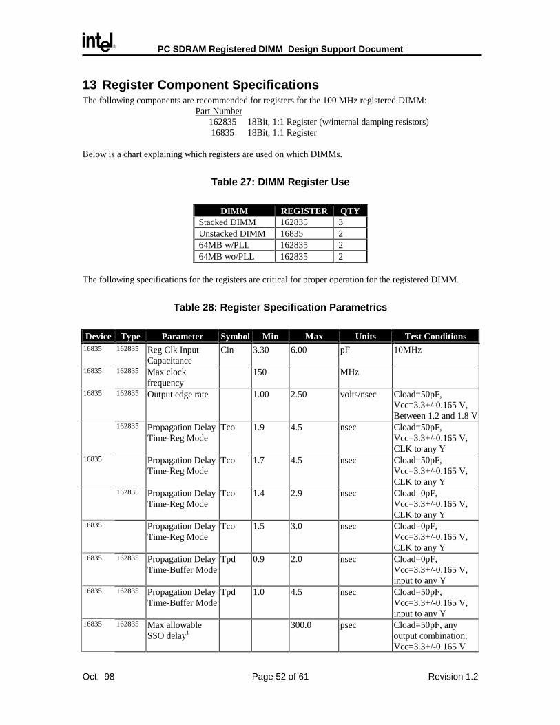
Figure 32: I-V Characteristics for 16835 Register Output – Pull Down
16835 Register IBIS I/V Pull-up Char.
-250.0
-200.0
-150.0
-100.0
-50.0
0.0
50.0
0.0 1.0 2.0 3.0
V (volts)
I (m
A) Imin (mA)
Imax (mA)
Figure 33: I-V Characteristics for 16835 Register Output – Pull Up

PC SDRAM Registered DIMM Design Support Document
Oct. 98 Page 55 of 61 Revision 1.2
Table 29: 16835 I-V Data
Pulldown PulllupV (volts) Imin
(mA)Imax (mA) V (volts) Imin (mA) Imax
(mA)0.0 0.0 0.0 3.0 0.0 0.00.1 9.3 22.6 2.9 -6.6 -15.60.2 17.9 43.5 2.8 -12.9 -30.60.3 26.0 62.7 2.7 -18.8 -44.80.4 33.5 80.3 2.6 -24.5 -58.30.5 40.4 96.5 2.5 -29.8 -71.20.6 46.7 111.2 2.4 -34.8 -83.30.7 52.6 124.7 2.3 -39.5 -94.90.8 57.9 136.9 2.2 -43.9 -105.70.9 62.7 148.0 2.1 -48.0 -115.91.0 67.0 157.9 2.0 -51.8 -125.51.1 70.9 166.8 1.9 -55.3 -134.41.2 74.3 174.7 1.8 -58.4 -142.71.3 77.3 181.7 1.7 -61.3 -150.41.4 79.9 187.8 1.6 -63.9 -157.51.5 82.0 193.1 1.5 -66.2 -164.01.6 83.7 197.5 1.4 -68.2 -169.91.7 85.1 201.2 1.3 -70.0 -175.21.8 86.0 204.2 1.2 -71.4 -180.01.9 86.6 206.4 1.1 -72.5 -184.22.0 86.8 208.0 1.0 -73.4 -187.82.1 87.0 209.0 0.9 -73.8 -190.92.2 87.2 209.4 0.8 -74.3 -193.42.3 87.4 209.8 0.7 -74.7 -195.42.4 87.6 210.3 0.6 -75.1 -196.62.5 87.8 210.7 0.5 -75.5 -197.62.6 88.0 211.1 0.4 -75.9 -198.52.7 88.2 211.6 0.3 -76.4 -199.52.8 88.4 212.0 0.2 -76.8 -200.52.9 88.6 212.4 0.1 -77.2 -201.53.0 88.8 212.9 0.0 -77.7 -202.63.1 89.0 213.33.2 89.2 213.83.3 89.4 214.23.4 89.6 214.63.5 89.9 215.13.6 90.7 215.5

PC SDRAM Registered DIMM Design Support Document
Oct. 98 Page 56 of 61 Revision 1.2
162835 Register IBIS I/V Pulldown Char.
-20.0
0.0
20.0
40.0
60.0
80.0
100.0
120.0
0.0 1.0 2.0 3.0 4.0
V (volts)
I (m
A) Imin (mA)
Imax (mA)
Figure 34: I-V Characteristics for 162835 Register Output – Pull Down
162835 IBIS I/V Pull-up Char
-100.0
-90.0
-80.0
-70.0
-60.0
-50.0
-40.0
-30.0
-20.0
-10.0
0.0
10.0
0 0.5 1 1.5 2 2.5 3
V (volts)
I (m
A) I(min)
I(max)
Figure 35: I-V Characteristics for 162835 Register Output – Pull Up

PC SDRAM Registered DIMM Design Support Document
Oct. 98 Page 57 of 61 Revision 1.2
Table 30: 162835 I-V Data
Pulldown PulllupV (volts) Imin (mA) Imax (mA) V (volts) Imax (mA) Imin (mA)
0.0 0.0 0.0 3.0 0.0 0.00.1 2.7 3.3 2.9 -3.1 -2.40.2 5.5 6.6 2.8 -6.2 -4.90.3 8.2 9.9 2.7 -9.3 -7.30.4 10.9 13.2 2.6 -12.4 -9.70.5 13.5 16.5 2.5 -15.4 -12.10.6 16.2 19.7 2.4 -18.5 -14.40.7 18.8 23.0 2.3 -21.6 -16.80.8 21.4 26.3 2.2 -24.6 -19.10.9 24.0 29.5 2.1 -27.7 -21.41.0 26.6 32.8 2.0 -30.7 -23.71.1 29.2 36.0 1.9 -33.8 -25.91.2 31.7 39.3 1.8 -36.8 -28.11.3 34.2 42.5 1.7 -39.8 -30.41.4 36.7 45.7 1.6 -42.8 -32.51.5 39.2 48.9 1.5 -45.9 -34.71.6 41.6 52.2 1.4 -48.9 -36.81.7 44.0 55.4 1.3 -51.9 -38.91.8 46.4 58.6 1.2 -54.9 -41.01.9 48.7 61.7 1.1 -57.8 -43.12.0 51.0 64.9 1.0 -60.8 -45.12.1 53.3 68.1 0.9 -63.8 -47.12.2 55.6 71.3 0.8 -66.7 -49.02.3 57.8 74.4 0.7 -69.7 -50.92.4 59.9 77.5 0.6 -72.6 -52.82.5 62.1 80.7 0.5 -75.6 -54.62.6 64.1 83.8 0.4 -78.5 -56.42.7 66.2 86.9 0.3 -81.4 -58.12.8 68.2 90.0 0.2 -84.3 -59.82.9 70.1 93.1 0.1 -87.2 -61.43.0 72.0 96.2 0.0 -90.1 -63.03.1 73.8 99.33.2 75.5 102.43.3 77.2 105.43.4 78.7 108.43.5 80.2 111.5

PC SDRAM Registered DIMM Design Support Document
Oct. 98 Page 58 of 61 Revision 1.2
14 PLL Component SpecificationsThe following components are recommended for the PLL for the 100 MHz registered DIMM:
Part Number2509 1:9 PLL Based Clock Driver2510 1:10 PLL Based Clock Driver
The following specifications for the PLL are critical in proper operation for the registered DIMM.
Table 31: PLL Component Specifications
Parameter Symbol Min Max Units Test Conditions
PLL Clk Input Capacitance Cin 2.50 6.00 pF 10MHz
PLL Feedback InputCapacitance
Cin 2.50 6.00 pF 10MHz
Input clock rise/fall edge rate 1.00 2.50 volts/nsec
Output rise/fall edge rate 1.00 2.50 volts/nsec Cload=50pF, Vcc=3.3+/-0.165 V,Between 1.2 and 1.8 V
Input clock duty cycle 40 60 %
Output clock duty cycle 45 55 %
Operating Frequency Range 50 125 MHz
Operating temperature range Tcase 0 85 deg C
Operating Voltage range forspecification
3.135 3.465 volts
Output stabilization time 1 msec After power up
Analog power supply rejection 100 mV, pk-pk DC to 10MHz
Output clock(n) to clock(n+1)jitter
-100 100 psec with and w/o Spread Spectrum Clock(SSC) Input 1
Output to output skew Tskew 200 psec
SSC Induced skew -200 200 psec See below
Static Phase Error Tspe -150 150 psec 66 MHz<f<100 MHz, 0pF feedbackload
Phase Error –Jitter -50 50 psec f>66 MHz
Input current Iin -5 5 uA
Power dissipation 700 mW 55C free-air ambient
1 SSC(Spread Spectrum Clock) Induced Skew: SSC clock synthesizers are commonly used on system motherboards to reduce EMI. The PLL used on PC100 registered DIMMs must be capable of meeting all of the above test parameters while supporting SSC synthesizers with the following parameters:
Min Max Units
SSC modulation frequency 30.00 50.00 KHz
SSC clock input frequencydeviation
0.00 0.50 % ie freq range for 100 MHz is 99.5 to100 MHz
-PLL designs should target the values below to meet the 200ps maximum of SSC induced skew:
Min Max Units
PLL loop bandwidth 1.20 MHz
Phase angle -0.031 degrees

PC SDRAM Registered DIMM Design Support Document
Oct. 98 Page 59 of 61 Revision 1.2
Below is a chart explaining which PLLs are used on which DIMMs.
Table 32: DIMM PLL Use
DIMM PLL
Stacked DIMM 2510UnstackedDIMM
2509
64MB w/PLL 250964MB wo/PLL NA
The Output Buffers for all PLL’s used for these designs must conform within the followingMin/Max I/V Range:

PC SDRAM Registered DIMM Design Support Document
Oct. 98 Page 60 of 61 Revision 1.2
PLL PULLUP IBIS I/V Char.
-100.0
-90.0
-80.0
-70.0
-60.0
-50.0
-40.0
-30.0
-20.0
-10.0
0.0
10.0
0 0.5 1 1.5 2 2.5 3
V (volts)
I (m
A) Spec I(min)
Spec I(max)
Figure 36: I-V Characteristics for PLL Output – Pull up
PLL PULLDOWN IBIS I/V Char
-20.0
0.0
20.0
40.0
60.0
80.0
100.0
120.0
0 0.5 1 1.5 2 2.5 3 3.5
V (volts)
I (m
A) Spec I(min)
Spec I(max)
Figure 37: I-V Characteristics for PLL Output – Pull Down

PC SDRAM Registered DIMM Design Support Document
Oct. 98 Page 61 of 61 Revision 1.2
The Output Buffer I/V data for all PLL’s is listed for reference:
Table 33: PLL Output I-V Data
Pulldown PullupV(Volts) Imin(mA) Imax(mA) V(Volts) Imin(mA) Imax(mA)
0 0.0 0 3 0.0 0.00.1 2.1 3.30401 2.9 -2.1 -3.10.2 4.1 6.60266 2.8 -4.1 -6.20.3 6.2 9.89585 2.7 -6.1 -9.30.4 8.2 13.1835 2.6 -8.0 -12.40.5 10.1 16.4654 2.5 -10.0 -15.40.6 12.1 19.7415 2.4 -11.9 -18.50.7 14.0 23.0116 2.3 -13.9 -21.60.8 15.8 26.2757 2.2 -15.7 -24.60.9 17.7 29.5336 2.1 -17.6 -27.71 19.5 32.7852 2 -19.4 -30.71.1 21.3 36.0302 1.9 -21.3 -33.81.2 23.0 39.2687 1.8 -23.1 -36.81.3 24.7 42.5003 1.7 -24.8 -39.81.4 26.3 45.725 1.6 -26.6 -42.81.5 27.9 48.9426 1.5 -28.3 -45.91.6 29.5 52.1529 1.4 -29.9 -48.91.7 31.0 55.3557 1.3 -31.6 -51.91.8 32.4 58.5509 1.2 -33.2 -54.91.9 33.9 61.7382 1.1 -34.7 -57.82 35.2 64.9175 1 -36.3 -60.82.1 36.5 68.0885 0.9 -37.7 -63.82.2 37.7 71.2511 0.8 -39.2 -66.72.3 38.9 74.4049 0.7 -40.6 -69.72.4 39.9 77.5498 0.6 -41.9 -72.62.5 40.9 80.6855 0.5 -43.2 -75.62.6 41.9 83.8117 0.4 -44.5 -78.52.7 42.7 86.9282 0.3 -45.7 -81.42.8 43.4 90.0347 0.2 -46.8 -84.32.9 44.1 93.1308 0.1 -47.9 -87.23 44.7 96.2163 0 -48.9 -90.13.1 45.1 99.29093.2 45.6 102.3543.3 45.9 105.4063.4 46.2 108.4453.5 46.5 111.472