pci express 3.0 testing approaches for phy layer · 2017-08-07 · pci express 3.0 testing...
TRANSCRIPT

PCI Express 3.0 Testing Approaches for PHY Layer
2011/5/32
PCI Express 3.0 Technology Timeline
Silicon Phase
Integration Phase
– Product Development– PCI-SIG Tool Development
Deployment Phase
– CEM Spec Development
Tektronix Involved in PCIe EWG, CEM, and SEG Working Groups
Estimated Date
Released Date
All Information is this presentation is based on 1.0 Base Specification
0.710.5 0.7
Base Spec
CEM Spec0.5 Release 0.7
Test Spec0.3 Release
0.9 1.0
2009
Q1 Q2 Q3 Q4 Q1 Q2 Q3 Q4 Q1 Q2 Q3 Q4 Q1 Q2 Q3 Q4
2010 2011 2012
0.9 1.0
0.5 0.7 0.9 1.0
6 Month FYI TestingFYI Testing
2011/5/33
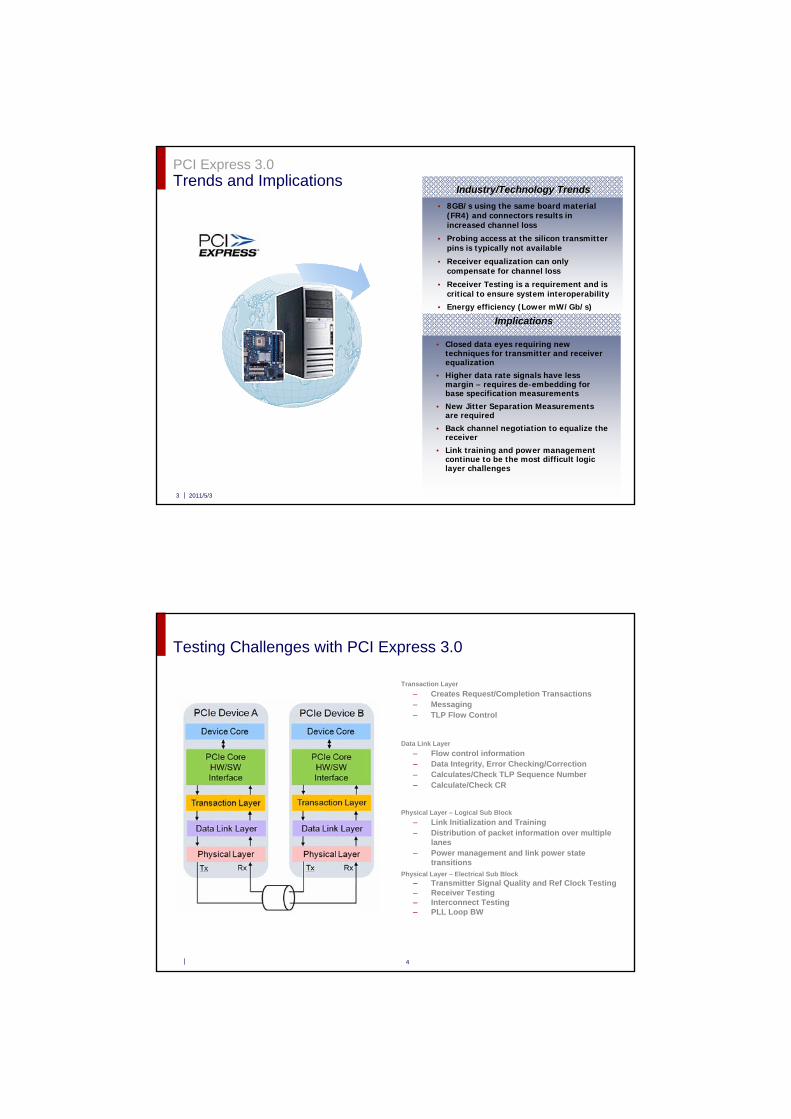
PCI Express 3.0Trends and Implications
• 8GB/s using the same board material (FR4) and connectors results in increased channel loss
• Probing access at the silicon transmitter pins is typically not available
• Receiver equalization can only compensate for channel loss
• Receiver Testing is a requirement and is critical to ensure system interoperability
• Energy efficiency (Lower mW/Gb/s)
Industry/Technology Trends
• Closed data eyes requiring new techniques for transmitter and receiver equalization
• Higher data rate signals have less margin – requires de-embedding for base specification measurements
• New Jitter Separation Measurements are required
• Back channel negotiation to equalize the receiver
• Link training and power management continue to be the most difficult logic layer challenges
Implications
Testing Challenges with PCI Express 3.0
4
Physical Layer – Logical Sub Block
– Link Initialization and Training– Distribution of packet information over multiple
lanes– Power management and link power state
transitions
Data Link Layer
– Flow control information– Data Integrity, Error Checking/Correction– Calculates/Check TLP Sequence Number– Calculate/Check CR
Transaction Layer
– Creates Request/Completion Transactions– Messaging– TLP Flow Control
Physical Layer – Electrical Sub Block
– Transmitter Signal Quality and Ref Clock Testing– Receiver Testing– Interconnect Testing– PLL Loop BW
2011/5/35
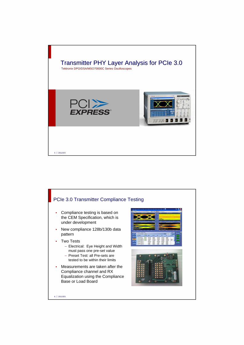
Transmitter PHY Layer Analysis for Transmitter PHY Layer Analysis for PCIePCIe 3.03.0Tektronix DPO/DSA/MSO70000C Series Oscilloscopes
2011/5/36
PCIe 3.0 Transmitter Compliance Testing
• Compliance testing is based on the CEM Specification, which is under development
• New compliance 128b/130b data pattern
• Two Tests– Electrical: Eye Height and Width
must pass one pre-set value– Preset Test: all Pre-sets are
tested to be within their limits
• Measurements are taken after the Compliance channel and RX Equalization using the Compliance Base or Load Board

2011/5/37
Add-In Card Compliance Signal Acquisition and Processing
Signal Acquiredfrom ComplianceBoard
Embed the Add-In CardCompliance Channel
Closed Eye due tothe Channel
Apply the Base Specification CTLE + Dfefor Long Channel
Open Eye for Measurements
System Board Eye Limits 1
Add-In Card Eye Limits 1
Parameter Min Max Units
VTXSVTXS_d
3434
12001200
mVmV
TTXS 41.25 ps
Parameter Min Max Units
VTXAVTXA_d
3434
12001200
mVmV
TTXA 41.25 ps
1 Measurement Limits Under CEM Review
2011/5/38
Serial Data Link Analysis
• De-embed the effects of a fixture
• Embed the effects of the channel
• Equalize the waveform using CTLE, FFE, and/or Dfe
2011/5/39
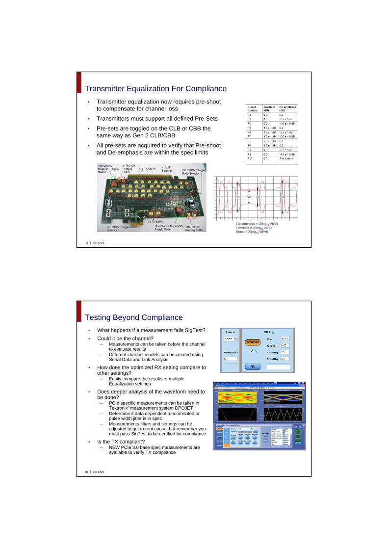
Transmitter Equalization For Compliance
• Transmitter equalization now requires pre-shoot to compensate for channel loss
• Transmitters must support all defined Pre-Sets
• Pre-sets are toggled on the CLB or CBB the same way as Gen 2 CLB/CBB
• All pre-sets are acquired to verify that Pre-shoot and De-emphasis are within the spec limits
2011/5/310
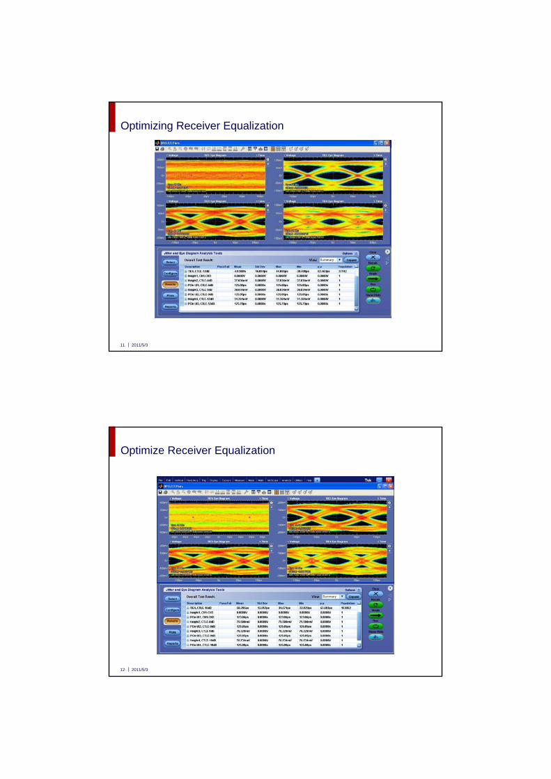
Testing Beyond Compliance
• What happens if a measurement fails SigTest?
• Could it be the channel?– Measurements can be taken before the channel
to evaluate results– Different channel models can be created using
Serial Data and Link Analysis
• How does the optimized RX setting compare to other settings?
– Easily compare the results of multiple Equalization settings
• Does deeper analysis of the waveform need to be done?
– PCIe specific measurements can be taken in Tektronix’ measurement system DPOJET
– Determine if data dependent, uncorrelated or pulse width jitter is in spec
– Measurements filters and settings can be adjusted to get to root cause, but remember you must pass SigTest to be certified for compliance
• Is the TX compliant?– NEW PCIe 3.0 base spec measurements are
available to verify TX compliance
2011/5/311
Optimizing Receiver Equalization
2011/5/312
Optimize Receiver Equalization
2011/5/313
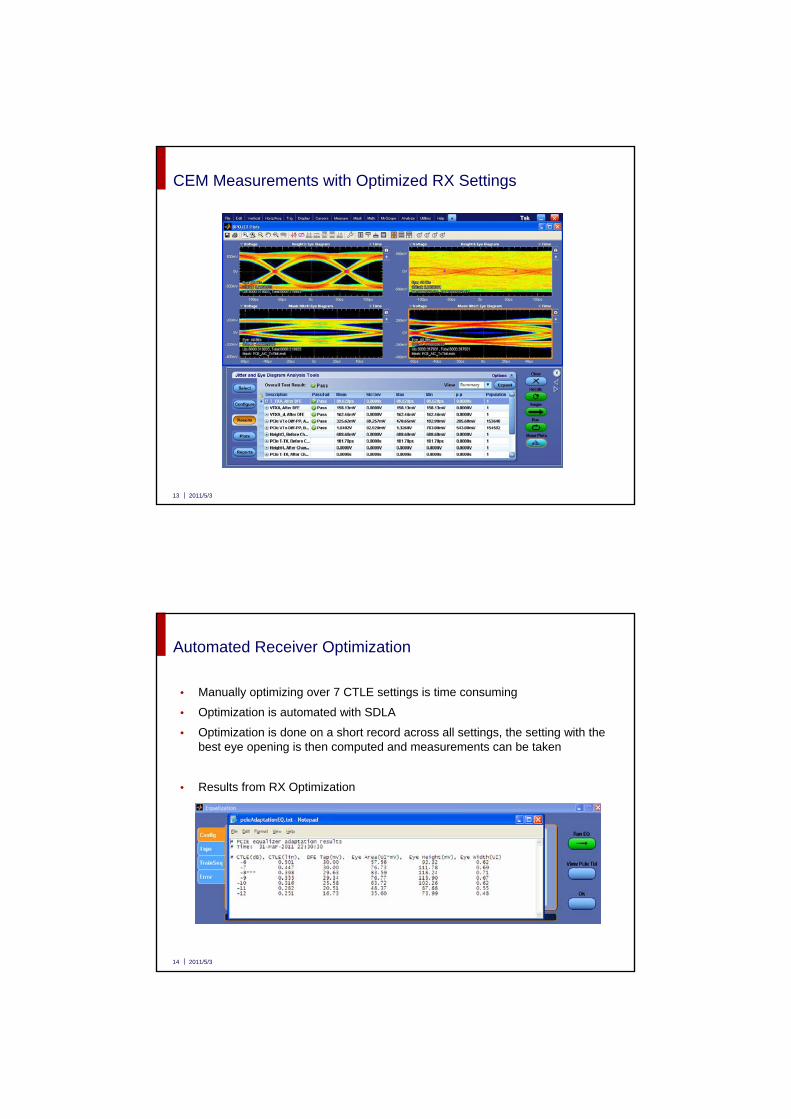
CEM Measurements with Optimized RX Settings
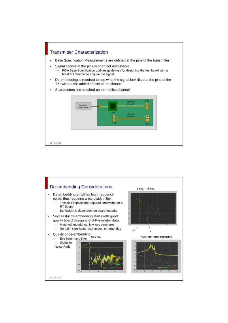
Automated Receiver Optimization
• Manually optimizing over 7 CTLE settings is time consuming
• Optimization is automated with SDLA
• Optimization is done on a short record across all settings, the setting with the best eye opening is then computed and measurements can be taken
• Results from RX Optimization
2011/5/314
2011/5/315
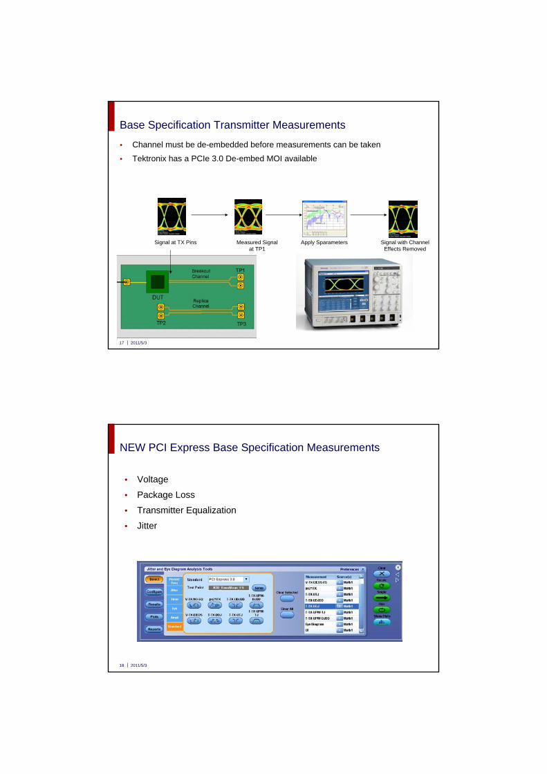
• Base Specification Measurements are defined at the pins of the transmitter
• Signal access at the pins is often not assessable – PCIe Base Specification outlines guidelines for designing the test board with a
breakout channel to acquire the signal
• De-embedding is required to see what the signal look liked at the pins of the TX, without the added effects of the channel
• Sparameters are acquired on the replica channel
Transmitter Characterization
2011/5/316
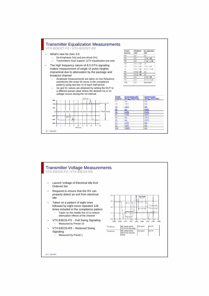
De-embedding Considerations
• De-embedding amplifies high frequency noise, thus requiring a bandwidth filter
– This also impacts the required bandwidth for a RT Scope
– Bandwidth is dependent on board material
• Successful de-embedding starts with good quality board design and S-Parameter data
– Matched impedance, low loss structures– No gain, significant resonances, or large dips
• Quality of de-embedding– Eye height and jitter– Signal to Noise Ratio
5 GHz 10 GHz
5GHz Filter 10GHz Filter -> Noise amplification
2011/5/317
• Channel must be de-embedded before measurements can be taken
• Tektronix has a PCIe 3.0 De-embed MOI available
Base Specification Transmitter Measurements
Signal at TX Pins Measured Signalat TP1
Apply Sparameters Signal with ChannelEffects Removed
2011/5/318
NEW PCI Express Base Specification Measurements
• Voltage
• Package Loss
• Transmitter Equalization
• Jitter
2011/5/319
Transmitter Equalization MeasurementsVTX-BOOST-FS / VTX-BOOST-RS
• What’s new for Gen 3.0– De-Emphasis (Va) and pre-shoot (Vc)– Transmitters must support 11TX equalization pre-sets
• The high frequency nature of 8.0 GT/s signaling makes measurement of single UI pulse heights impractical due to attenuation by the package and breakout channel
– Amplitude measurements are taken on low frequency waveforms (64 ones/ 64 zeros in the compliance pattern) using last few UI of each half period
– Va and Vc values are obtained by setting the DUT to a different preset value where the desired Va or Vcvoltage occurs during the Vb interval.
2011/5/320
Transmitter Voltage MeasurementsVTX-EIEOS-FS / VTX-EIEOS-RS
• Launch Voltage of Electrical Idle Exit Ordered Set
• Required to ensure that the RX can properly detect an exit from electrical idle
• Taken on a pattern of eight ones followed by eight zeros repeated 128 times included in the compliance pattern
– Taken on the middle five UI to reduce attenuation effects of the channel
• VTX-EIEOS-FS - Full Swing Signaling– Measured by Preset 10
• VTX-EIEOS-RS – Reduced Swing Signaling
– Measured by Preset 1
2011/5/321
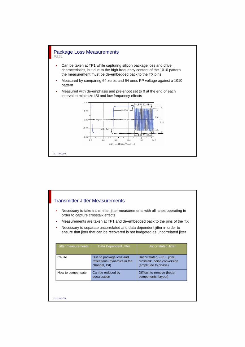
Package Loss MeasurementsPS21
• Can be taken at TP1 while capturing silicon package loss and drive characteristics, but due to the high frequency content of the 1010 pattern the measurement must be de-embedded back to the TX pins
• Measured by comparing 64 zeros and 64 ones PP voltage against a 1010 pattern
• Measured with de-emphasis and pre-shoot set to 0 at the end of each interval to minimize ISI and low frequency effects
2011/5/322
Transmitter Jitter Measurements
• Necessary to take transmitter jitter measurements with all lanes operating in order to capture crosstalk effects
• Measurements are taken at TP1 and de-embedded back to the pins of the TX
• Necessary to separate uncorrelated and data dependent jitter in order to ensure that jitter that can be recovered is not budgeted as uncorrelated jitter
Jitter measurements Data Dependent Jitter Uncorrelated Jitter
Cause Due to package loss and reflections (dynamics in the channel, ISI)
Uncorrelated - PLL jitter, crosstalk, noise conversion (amplitude to phase)
How to compensate Can be reduced by equalization
Difficult to remove (better components, layout)
2011/5/323
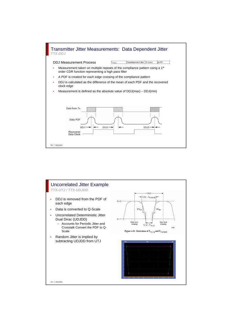
Transmitter Jitter Measurements: Data Dependent JitterTTX-DDJ
DDJ Measurement Process
• Measurement taken on multiple repeats of the compliance pattern using a 1st
order CDR function representing a high pass filter
• A PDF is created for each edge crossing of the compliance pattern
• DDJ is calculated as the difference of the mean of each PDF and the recovered clock edge
• Measurement is defined as the absolute value of DDJ(max) – DDJ(min)
2011/5/324
Uncorrelated Jitter ExampleTTX-UTJ / TTX-UDJDD
• DDJ is removed from the PDF of each edge
• Data is converted to Q-Scale
• Uncorrelated Deterministic Jitter Dual Dirac (UDJDD)
– Accounts for Periodic Jitter and Crosstalk Convert the PDF to Q-Scale
• Random Jitter is implied by subtracting UDJDD from UTJ
2011/5/325
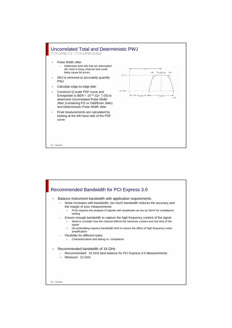
Uncorrelated Total and Deterministic PWJTTX-UPW-TJ / TTX-UPW-DJDD
• Pulse Width Jitter– Addresses lone bits that are attenuated
the most in lossy channel and could likely cause bit errors
• DDJ is removed to accurately quantify PWJ
• Calculate edge-to-edge jitter
• Construct Q-scale PDF curve and Extrapolate to BER = 10-12 (Q= 7.03) to determine Uncorrelated Pulse Width Jitter (containing F/2 or Odd/Even Jitter) and Deterministic Pulse Width Jitter
• Final measurements are calculated by looking at the left hand side of the PDF curve
2011/5/326
Recommended Bandwidth for PCI Express 3.0
• Balance instrument bandwidth with application requirements– Noise increases with bandwidth, too much bandwidth reduces the accuracy and
the margin of your measurements• PCIe requires the analysis of signals with amplitudes as low as 34mV for compliance
testing
– Ensure enough bandwidth to capture the high frequency content of the signal• Need to consider how the channel effects the harmonic content and rise time of the
signal • De-embedding requires bandwidth limit to reduce the effect of high frequency noise
amplification
– Flexibility for different tasks• Characterization and debug vs. compliance
• Recommended bandwidth of 16 GHz– Recommended: 16 GHz best balance for PCI Express 3.0 Measurements– Minimum: 12 GHz

2011/5/327
Tektronix Solutions for PCI Express 3.0 Measurements
• Introducing option PCE3 for DSA/DPO/MSO70K Scopes
• Support for NEW Base Spec measurements
• Support for CEM Specification
• Supports all versions of PCI Express
2011/5/328
Considerations for Test Equipment Selection
• Test solutions need to go beyond compliance to enable enable root cause analysis
• Channel Embedding and Receiver equalization require new solutions that enable characterizing the optimal settings
• Solutions need to evolve as the test specifications are under development
• Tektronix’ has the solutions you need to begin your PCIe 3.0 testing today – Active participation in industry working groups enable software updates as the specification
evolves– PCE3 is not just a compliance solution - spans multiple tasks from Compliance, Characterization,
and Debug – Complete tools for channel modeling (embedding / de-embedding) and receiver equalization
Serial Data and Link Analysis Software (SDLA)– New DPO/DSA/MSO70000C Series Oscilloscopes
• Provides lower noise and jitter with 100GS/s acquisition • New Compute Platform reduces overall test time
2011/5/329
Receiver PHY Layer Analysis for Receiver PHY Layer Analysis for PCIePCIe 3.03.0Tektronix BSA85C Bit Error Rate Tester
2011/5/330
PCIe 3.0 Implications for Receiver Testing• System margins are decreasing, testing the transmitter only does not imply
interoperability
• Receiver testing is expected to be mandatory and will include testing with a Stressed Voltage and Stressed Jitter Eye
– Differential and Common Mode Interference are new impairment requirements
• Transmitter Equalization requires De-Emphasis and Pre-Shoot
• Receiver Equalization is more sophisticated– Behavior equalizers (Continuous Time Linear and Decision Feedback Equalization)
must be used to compensate for channel loss– Transmitters must support back channel negotiation to auto-negotiate with
Receivers to determine optimal equalization settings for testing
10 1 1 1 10 0 0 0 00 1 1 0 10 0 0 0
Bit Errors
2011/5/331
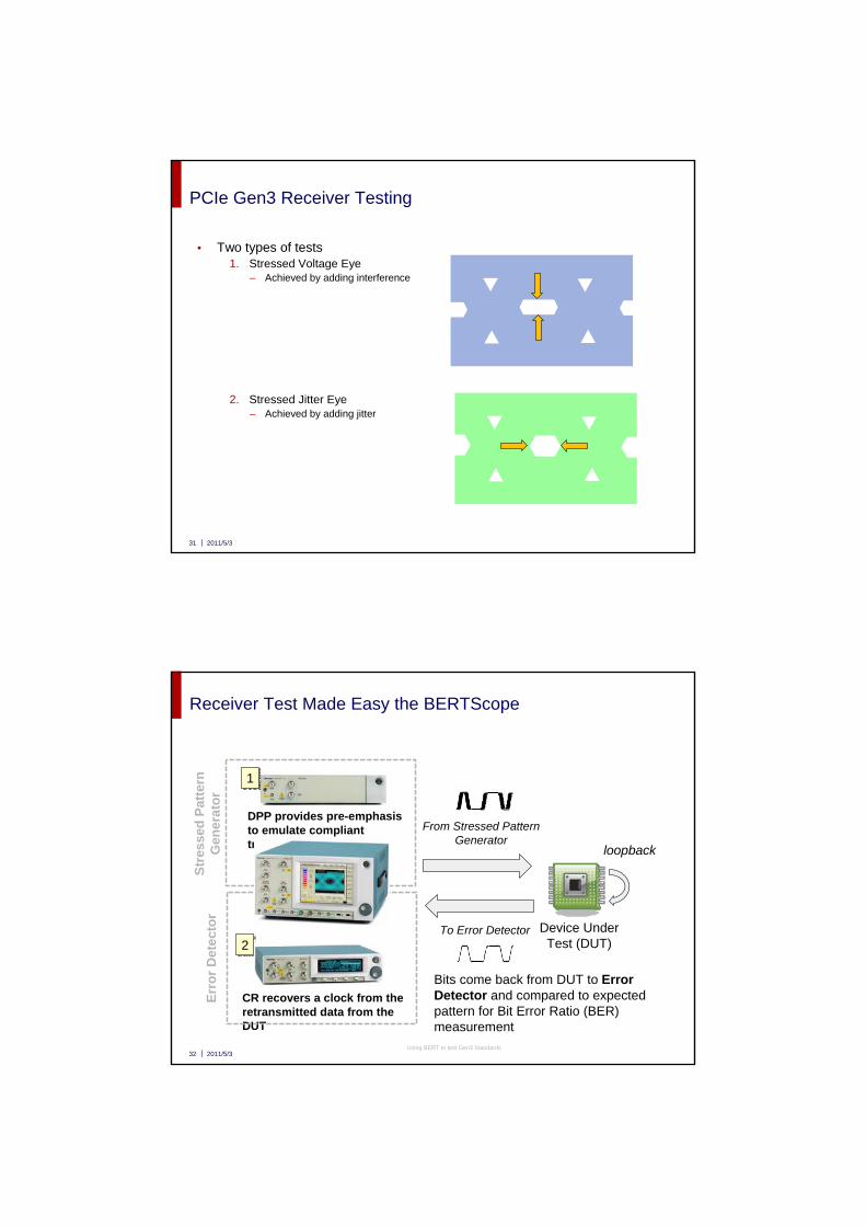
PCIe Gen3 Receiver Testing
• Two types of tests 1. Stressed Voltage Eye
– Achieved by adding interference
2. Stressed Jitter Eye– Achieved by adding jitter
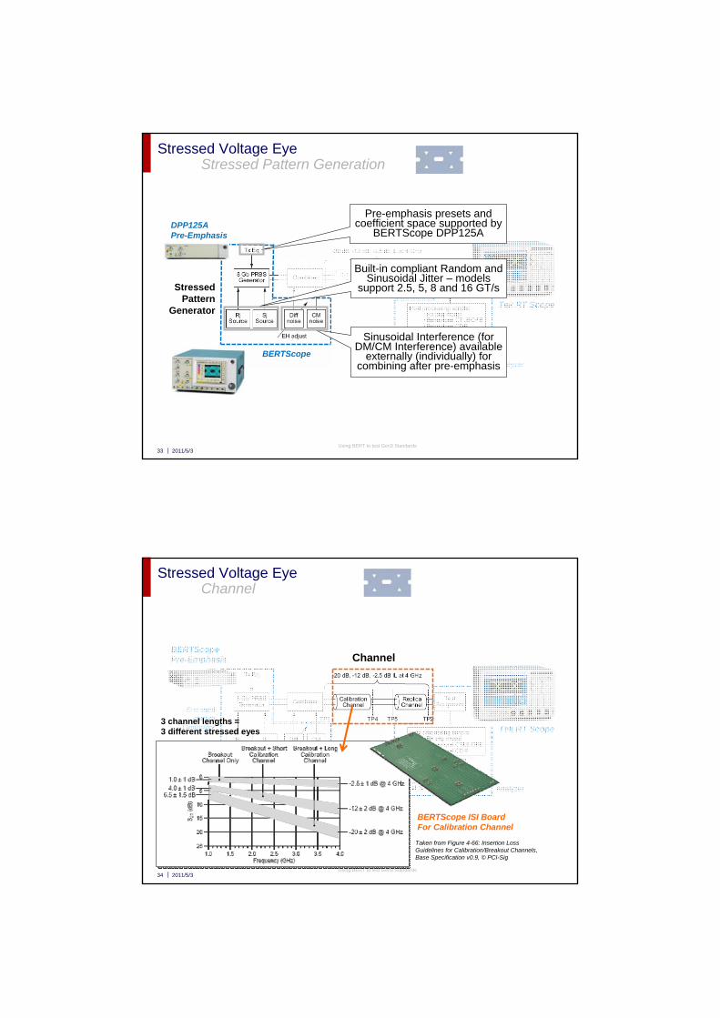
2011/5/332Using BERT to test Gen3 Standards
Device Under Test (DUT)
From Stressed Pattern Generator
To Error Detector
loopback
DPP provides pre-emphasis to emulate compliant transmitter
CR recovers a clock from the retransmitted data from the DUT
Str
ess
ed P
atte
rn
Gen
erat
or
Err
or
Det
ect
or
22
Bits come back from DUT to Error Detector and compared to expected pattern for Bit Error Ratio (BER) measurement
11
Receiver Test Made Easy the BERTScope
2011/5/333Using BERT to test Gen3 Standards
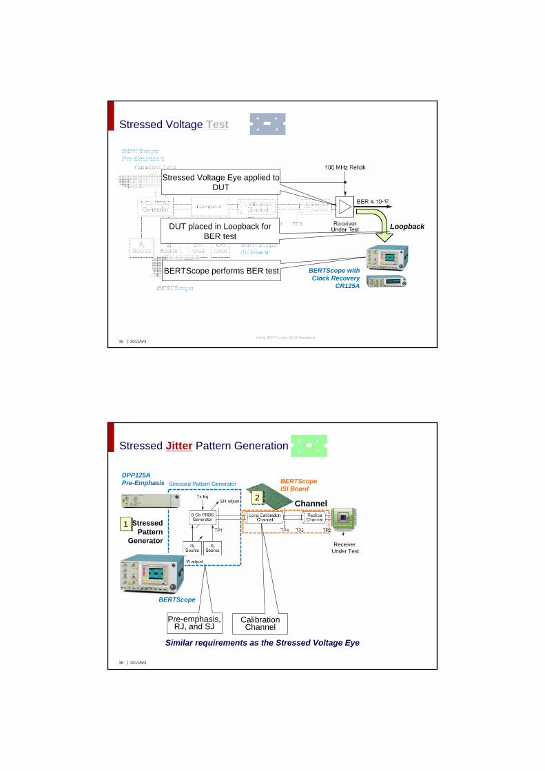
Stressed Voltage EyeStressed Pattern Generation
AnalyzerBERTScope
DPP125APre-Emphasis
Tek RT Scope
Pre-emphasis presets and coefficient space supported by
BERTScope DPP125A
Built-in compliant Random and Sinusoidal Jitter – models
support 2.5, 5, 8 and 16 GT/s
Sinusoidal Interference (for DM/CM Interference) available
externally (individually) for combining after pre-emphasis
Stressed Pattern
Generator
2011/5/334Using BERT to test Gen3 Standards
Stressed Voltage EyeChannel
Stressed Pattern
Generator
Analyzer
BERTScopePre-Emphasis
Tek RT Scope
BERTScope ISI BoardFor Calibration Channel
3 channel lengths = 3 different stressed eyes
Channel
Taken from Figure 4-66: Insertion Loss Guidelines for Calibration/Breakout Channels, Base Specification v0.9, © PCI-Sig
2011/5/335Using BERT to test Gen3 Standards
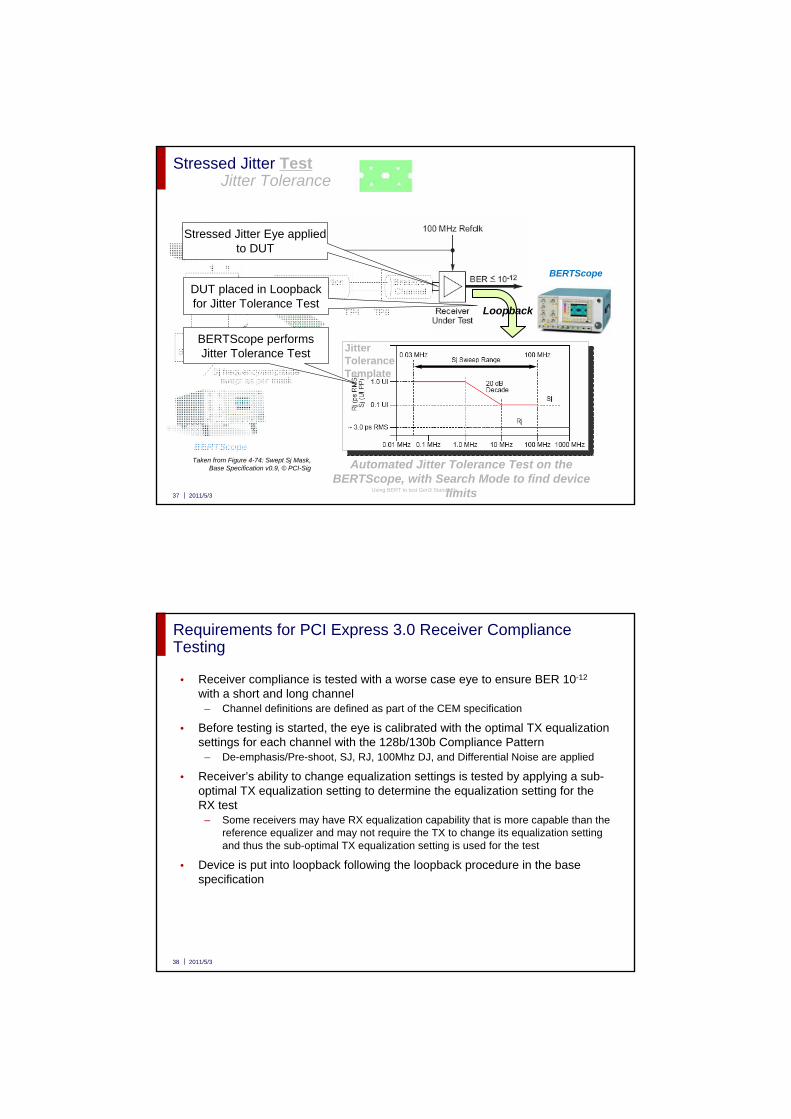
Stressed Voltage Test
Loopback
BERTScope
BERTScopeISI Board
BERTScopePre-Emphasis
BERTScope with Clock Recovery
CR125A
BERTScope performs BER test
Stressed Voltage Eye applied to DUT
DUT placed in Loopback for BER test
2011/5/336
Stressed Jitter Pattern Generation
Stressed Pattern Generator
BERTScope
Pre-emphasis, RJ, and SJ
Calibration Channel
BERTScopeISI Board
Similar requirements as the Stressed Voltage Eye
DPP125APre-Emphasis
Channel
11
22
Stressed Pattern
GeneratorReceiver
Under Test
2011/5/337Using BERT to test Gen3 Standards
Stressed Jitter TestJitter Tolerance
Loopback
BERTScope
BERTScopeISI Board
BERTScopePre-Emphasis
BERTScope
Automated Jitter Tolerance Test on the BERTScope, with Search Mode to find device
limits
Jitter Tolerance Template
BERTScope performs Jitter Tolerance Test
Stressed Jitter Eye applied to DUT
DUT placed in Loopbackfor Jitter Tolerance Test
Taken from Figure 4-74: Swept Sj Mask, Base Specification v0.9, © PCI-Sig
2011/5/338
Requirements for PCI Express 3.0 Receiver Compliance Testing
• Receiver compliance is tested with a worse case eye to ensure BER 10-12
with a short and long channel– Channel definitions are defined as part of the CEM specification
• Before testing is started, the eye is calibrated with the optimal TX equalization settings for each channel with the 128b/130b Compliance Pattern
– De-emphasis/Pre-shoot, SJ, RJ, 100Mhz DJ, and Differential Noise are applied
• Receiver’s ability to change equalization settings is tested by applying a sub-optimal TX equalization setting to determine the equalization setting for the RX test
– Some receivers may have RX equalization capability that is more capable than the reference equalizer and may not require the TX to change its equalization setting and thus the sub-optimal TX equalization setting is used for the test
• Device is put into loopback following the loopback procedure in the base specification
2011/5/339
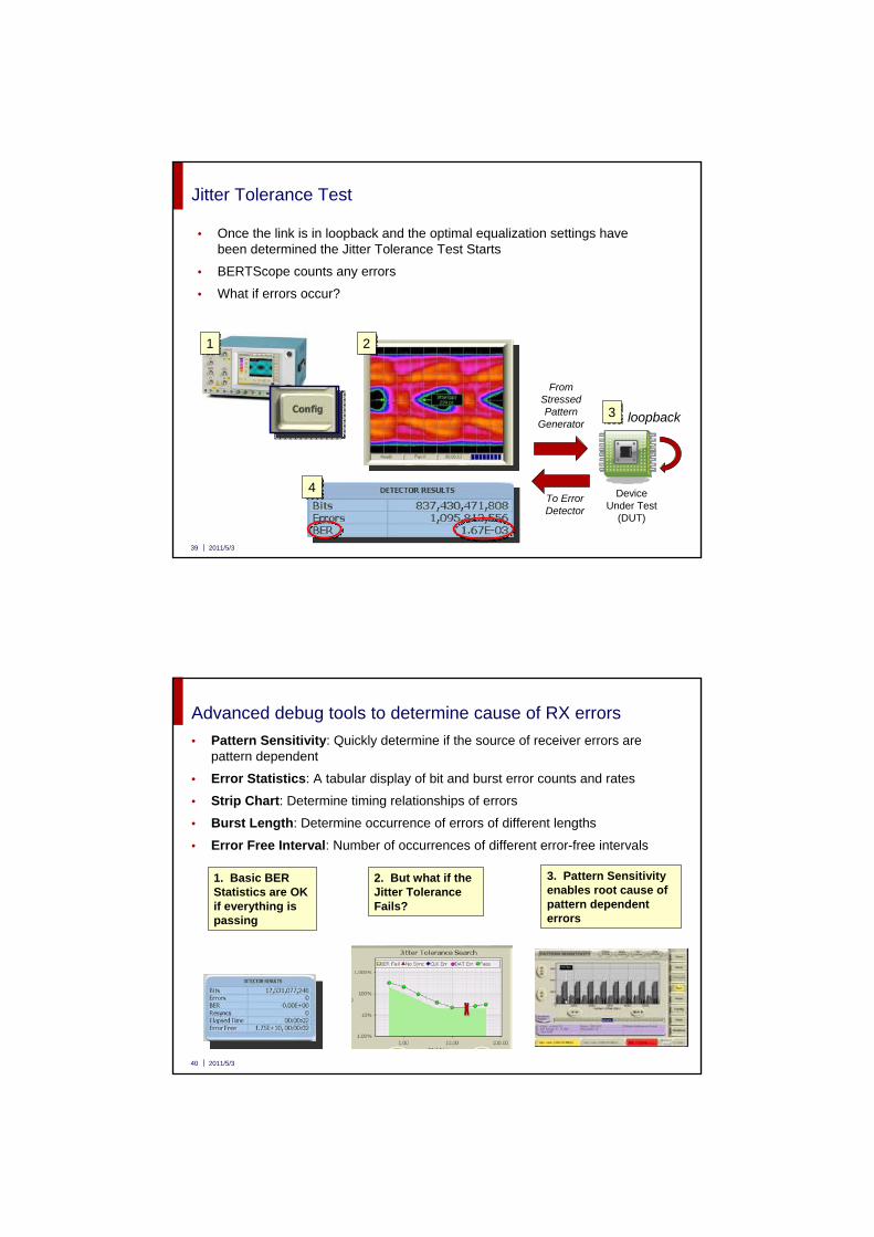
Device Under Test
(DUT)
loopback
11
33
From Stressed Pattern
Generator
To Error Detector
22
44
Jitter Tolerance Test
• Once the link is in loopback and the optimal equalization settings have been determined the Jitter Tolerance Test Starts
• BERTScope counts any errors
• What if errors occur?
2011/5/340
Advanced debug tools to determine cause of RX errors
BER
• Pattern Sensitivity: Quickly determine if the source of receiver errors are pattern dependent
• Error Statistics: A tabular display of bit and burst error counts and rates
• Strip Chart: Determine timing relationships of errors
• Burst Length: Determine occurrence of errors of different lengths
• Error Free Interval: Number of occurrences of different error-free intervals
BER
1. Basic BER Statistics are OK if everything is passing
2. But what if the Jitter Tolerance Fails?
3. Pattern Sensitivity enables root cause of pattern dependent errors

2011/5/341
Considerations for Receiver Test Equipment Selection
• Test solutions need to go beyond compliance to enable root cause analysis
• Transmitter Equalization requires generators that provide spec compliant De-emphasis and Pre-shoot
• Solutions need to evolve as the test specifications are under development
• Tektronix’ has the solutions you need to begin your PCIe 3.0 testing today– Advanced impairments enable verification of potential interoperability problems– Debug Tools enable root cause analysis of receiver errors– Quickly determine the margin of the DUT with user selectable jitter tolerance
algorithms– Loopback training sequence and compliance test patterns are available today– PCIe 3.0 Transmitter De-emphasis and Pre-shoot supported today
2011/5/342 2011/5/342
Important Resources• Complete Solutions Available on www.tek.com
– Solutions available today for PCIe 1.0, 2.0, 3.0 Transmitter, Receiver, PLL Loop bandwidth and Protocol Testing
• Support & Resource Links
– Recommended Equipment Configurations
www.tek.com/serial_data
– Access to new PCE3 Software Downloads & Free Trial
www.tek.com/software (search for PCE3)
– PCI Express Base Specification (members only)
http://www.pcisig.com/specifications/pciexpress/