pci express gen3 - keysight · make all connections to the unit before ... hardware and probing for...
TRANSCRIPT

Hardware and Probing Guide
PCI Express Gen3

Notices© Keysight Technologies 2011-2015
No part of this manual may be reproduced in any form or by any means (including electronic storage and retrieval or transla-tion into a foreign language) without prior agreement and written consent from Keysight Technologies as governed by United States and international copyright laws.
Trademarks
UNIX is a registered trademark of UNIX Sys-tem Laboratories in the U.S.A. and other countries. Target is copyrighted by Thru-Put Systems, Inc.
Manual Part NumberU4301-97000
Sixth Edition, October 2015
Available in electronic format only
Keysight Technologies1900 Garden of the Gods RoadColorado Springs, CO 80907 USA
Warranty
THE MATERIAL CONTAINED IN THIS DOCU-MENT IS PROVIDED "AS IS," AND IS SUB-JECT TO BEING CHANGED, WITHOUT NOTICE, IN FUTURE EDITIONS. FURTHER, TO THE MAXIMUM EXTENT PERMITTED BY APPLICABLE LAW, KEYSIGHT DISCLAIMS ALL WARRANTIES, EITHER EXPRESS OR IMPLIED WITH REGARD TO THIS MANUAL AND ANY INFORMATION CONTAINED HEREIN, INCLUDING BUT NOT LIMITED TO THE IMPLIED WARRANTIES OF MER-CHANTABILITY AND FITNESS FOR A PAR-TICULAR PURPOSE. KEYSIGHT SHALL NOT BE LIABLE FOR ERRORS OR FOR INCIDEN-TAL OR CONSEQUENTIAL DAMAGES IN CONNECTION WITH THE FURNISHING, USE, OR PERFORMANCE OF THIS DOCU-MENT OR ANY INFORMATION CONTAINED HEREIN. SHOULD KEYSIGHT AND THE
USER HAVE A SEPARATE WRITTEN AGREE-MENT WITH WARRANTY TERMS COVER-ING THE MATERIAL IN THIS DOCUMENT THAT CONFLICT WITH THESE TERMS, THE WARRANTY TERMS IN THE SEPARATE AGREEMENT WILL CONTROL.
Technology LicensesThe hardware and/or software described in this document are furnished under a license and may be used or copied only in accordance with the terms of such license.
U.S. Government Rights
The Software is "commercial computer software," as defined by Federal Acquisition Regulation ("FAR") 2.101. Pursuant to FAR 12.212 and 27.405-3 and Department of Defense FAR Supplement ("DFARS") 227.7202, the U.S. government acquires commercial computer software under the same terms by which the software is cus-tomarily provided to the public. Accord-ingly, Keysight provides the Software to U.S. government customers under its stan-dard commercial license, which is embod-ied in its End User License Agreement (EULA), a copy of which can be found at http://www.keysight.com/find/sweula. The license set forth in the EULA represents the exclusive authority by which the U.S. government may use, modify, distribute, or disclose the Software. The EULA and the license set forth therein, does not require or permit, among other things, that Key-sight: (1) Furnish technical information related to commercial computer software or commercial computer software docu-mentation that is not customarily provided to the public; or (2) Relinquish to, or other-wise provide, the government rights in excess of these rights customarily provided to the public to use, modify, reproduce, release, perform, display, or disclose com-mercial computer software or commercial computer software documentation. No
additional government requirements beyond those set forth in the EULA shall apply, except to the extent that those terms, rights, or licenses are explicitly required from all providers of commercial computer software pursuant to the FAR and the DFARS and are set forth specifically in writing elsewhere in the EULA. Keysight shall be under no obligation to update, revise or otherwise modify the Software. With respect to any technical data as defined by FAR 2.101, pursuant to FAR 12.211 and 27.404.2 and DFARS 227.7102, the U.S. government acquires no greater than Limited Rights as defined in FAR 27.401 or DFAR 227.7103-5 (c), as appli-cable in any technical data.
Safety Notices
CAUTIONA CAUTION notice denotes a hazard. It calls attention to an operating pro-cedure, practice, or the like that, if not correctly performed or adhered to, could result in damage to the product or loss of important data. Do not proceed beyond a CAUTION notice until the indicated conditions are fully understood and met.
WARNINGA WARNING notice denotes a hazard. It calls attention to an operating pro-cedure, practice, or the like that, if not correctly performed or adhered to, could result in personal injury or death. Do not proceed beyond a WARNING notice until the indicated conditions are fully understood and met.
2 PCI Express Gen3 Hardware and Probing Guide

PCI Express Gen3 Hardware and Probing Guide 3
Safety SummaryThe following general safety precautions must be observed during all phases of operation of this instrument. Failure to comply with these precautions or with specific warnings or operating instructions in the product manuals violates safety standards of design, manufacture, and intended use of the instrument. Keysight Technologies assumes no liability for the customer's failure to comply with these requirements. Product manuals are provided with your instrument on CD-ROM and/or in printed form. Printed manuals are an option for many products. Manuals may also be available on the Web. Go to www.keysight.com and type in your product number in the Search field at the top of the page.
General Do not use this product in any manner not specified by the manufacturer. The protective features of this product may be impaired if it is used in a manner not specified in the operation instructions.
Before Applying Power Verify that all safety precautions are taken. Make all connections to the unit before applying power. Note the instrument's external markings described in “Safety Symbols”.
Ground the Instrument If your product is provided with a grounding type power plug, the instrument chassis and cover must be connected to an electrical ground to minimize shock hazard. The ground pin must be firmly connected to an electrical ground (safety ground) terminal at the power outlet. Any interruption of the protective (grounding) conductor or disconnection of the protective earth terminal will cause a potential shock hazard that could result in personal injury.
Fuses See the user's guide or operator's manual for information about line-fuse replacement. Some instruments contain an internal fuse, which is not user accessible.
Do Not Operate in anExplosive Atmosphere
Do not operate the instrument in the presence of flammable gases or fumes.
Do Not Remove theInstrument Cover
Only qualified, service-trained personnel who are aware of the hazards involved should remove instrument covers. Always disconnect the power cable and any external circuits before removing the instrument cover.
Cleaning Clean the outside of the instrument with a soft, lint-free, slightly dampened cloth. Do not use detergent or chemical solvents.
Do Not Modify theInstrument
Do not install substitute parts or perform any unauthorized modification to the product. Return the product to an Keysight Sales and Service Office for service and repair to ensure that safety features are maintained.
In Case of Damage Instruments that appear damaged or defective should be made inoperative and secured against unintended operation until they can be repaired by qualified service personnel.

4 PCI Express Gen3 Hardware and Probing Guide
Safety Symbols
Table 1 Safety Symbol
CAUTIONA CAUTION notice denotes a hazard. It calls attention to an operating procedure, practice, or the like that, if not correctly performed or adhered to, could result in damage to the product or loss of important data. Do not proceed beyond a CAUTION notice until the indicated conditions are fully understood and met.
WARNINGA WARNING notice denotes a hazard. It calls attention to an operating procedure, practice, or the l ike that, if not correctly performed or adhered to, could resul t in personal injury or death. Do not proceed beyond a WARNING notice until the ind icated cond itions are fully understood and met.
Symbol Description
Direct current
Alternating current
Both direct and alternating current
Three phase alternating current
Three phase alternating current
Earth ground terminal
Protective earth ground terminal
Frame or chassis ground terminal
Terminal is at earth potential

PCI Express Gen3 Hardware and Probing Guide 5
Equipotentiality
N Neutral conductor on permanently installed equipment
L Line conductor on permanently installed equipment
On (mains supply)
Off (mains supply)
Standby (mains supply). The instrument is not completely disconnected from the mains supply when the power switch is in the standby position
In position of a bi-stable push switch
Out position of a bi-stable push switch
Equipment protected throughout by DOUBLE INSULATION or REINFORCED INSULATION
Caution, refer to accompanying documentation
Caution, risk of electric shock
Do not apply around or remove from HAZARDOUS LIVE conductors
Application around and removal from HAZARDOUS LIVE conductors is permitted
Caution, hot surface
Symbol Description

6 PCI Express Gen3 Hardware and Probing Guide
Ionizing radiation
CAT I IEC Measurement Category I
CAT II Measurement Category II
CAT III Measurement Category III
CAT IV Measurement Category IV
Symbol Description

PCI Express Gen3 Hardware and Probing Guide 7
Compliance and Environmental Information
Table 2 Compliance and Environmental Information
Safety Symbol Description
CSA is the Canadian certification mark to demonstrate compliance with the Safety requirements.
The C-tick mark is a registered trademark of the Spectrum ManagementAgency of Australia. This signifies compliance with the Australia EMCFramework regulations under the terms of the Radio Communication Actof 1992.
CE compliance marking to the EU Safety and EMC Directives.ISM GRP-1A classification according to the international EMC standard.ICES/NMB-001 compliance marking to the Canadian EMC standard.

8 PCI Express Gen3 Hardware and Probing Guide
Hardware and Probing for PCI Express Gen3—At a Glance
The PCIe Gen3 exerciser and protocol analyzer support all PCIe 3.0 speeds, including 2.5 GT/s (Gen1) and 5.0 GT/s (Gen2) through PCIe 8 GT/s (Gen3), and they support link widths from x1 to x16.
The U4305 PCIe Gen3 exerciser lets you use a link training sequencer state machine (LTSSM) exerciser to provide stimulus when testing links. The U4305 exerciser is a standard height, half-length card as described in the PCI Express specification, and fits into DUT or test backplane slots.
The U4301A/B PCIe Gen3 analyzer lets you capture and decode PCI Express data and view it in a Protocol Viewer window. The U4301A/B analyzer is a module (or modules) installed in an Keysight AXIe chassis (for example the M9502A portable 2-slot chassis).
You can use a U4301A/B analyzer module to capture data in a unidirectional (upstream or downstream upto x16 link width) setup or a bidirectional (upto x8 link width) setup. This module supports x1 to x8 bidirectional data capture using the same module.
There are currently the following DUT probing options for the U4301A/B analyzer module:
• U4321A Solid Slot Interposer
• U4322A Soft Touch midbus 3.0 probe
• U4324A PCIe Gen3 Flying Lead probe
• U4328A M.2 (M-key) Interposer
• U4330A U.2 SFF-8639 Interposer
See • "In This Guide" on page 9

PCI Express Gen3 Hardware and Probing Guide 9
In This GuideFor an overview and list of features, see: "Hardware and Probing for PCI Express Gen3—At a Glance" on page 8
This guide describes the probing options available for PCI Express Gen3 devices and how to make connections from the device under test (DUT) to the Keysight PCIe Gen3 protocol analyzer and exerciser modules.
See Also • For information on Keysight chassis, module, and software installation, see: "Keysight AXIe based Logic Analysis and Protocol Test Modules Installation Guide".
This guide is available on www.keysight.com and is also installed with the Logic Analyzer software.
• For information on using the protocol analysis application software, see the application software's online help.

10 PCI Express Gen3 Hardware and Probing Guide

PCI Express Gen3 Hardware and Probing Guide 11
ContentsSafety Summary 3
Compliance and Environmental Information 7
Hardware and Probing for PCI Express Gen3—At a Glance 8
In This Guide 9
1 U4305A/U4305B Exerciser Card
U4305A/U4305B Exerciser Card - Introduction 18
Features 19
Components 20Exerciser Card Status LEDs 23
U4305A/U4305B Exerciser Card as an Endpoint 26
U4305A/U4305B Exerciser Card as a Root Complex 27
Keep-Out Volume for U4305A/U4305B Exerciser Card 28
2 U4301A/B Analyzer Module
3 U4321A Solid Slot Interposer Card
U4321A Solid Slot Interposer Description 34
Setting up a bid irectional (x1-x8) configuration using a U4321A SSI Card 40
For a x8 bidirectional configuration 40For a x1, x2, or x4 bidirectional configuration 42

12 PCI Express Gen3 Hardware and Probing Guide
Contents
Setting up a unid irectional (x1-x16) configuration using a U4321A SSI Card 43
For a x16 downstream configuration 4344
For a x1, x2, x4, or x8 downstream configuration 45For a x16 upstream configuration 45
46For a x1, x2, x4, or x8 upstream configuration 47
Setting up a x16 upstream and downstream configuration using a U4321A SSI Card 48
U4321A Solid Slot Interposer Dimensions 50
4 Soft Touch Midbus 3.0 Probes
DUT Mechanical Design Considerations 54Footprint for Probe 54Keep-Out Volume for Probe and Retention Module Dimensions 57Footprint for Reference Clock Connector 58Keep-Out Volume for Reference Clock Connector 58
DUT Electrical Design Considerations 60Routing Considerations 60Load Model for Probe 62Electrical Requirements for Reference Clock Connector 63Load Model for Reference Clock Connector 63

PCI Express Gen3 Hardware and Probing Guide 13
Contents
Supported Footprint Pinouts and Pod Connections 64x16 Straight Footprint 64x16 Swizzled Footprint 67x16 Unidirectional Footprint 70x8 Bidirectional Footprint 72Two x8 Unidirectional Footprint 74Two x4 Bidirectional Footprint 76x4 Bidirectional Footprint 78Two x4 Unidirectional Footprint 80Two x2 Bidirectional Footprint 83Two x2 Unidirectional Footprint 85x1 Bi-directional Footprint 87Two x1 Bidirectional Footprint 89Two x1 Unidirectional Footprint 91
Probe Installation Instructions 93Bolting Probe Head and Retention Module onto DUT 93Inserting Probe Head into Retention Module on DUT 95
Probe Characteristics 97
5 PCIe Gen3 Flying Lead Probes
U4324A PCIe Gen3 Flying Lead Probe Description 100When to use a U4324A Flying Lead Probe 100Probe Components 100N5426A ZIF Tip 102Probe Characteristics 104
Install ing a U4324A Probe 106Providing Mechanical Strain Relief for the U4324A Probe Installations 107Labeling the probes 110
Supported Link Configurations 112

14 PCI Express Gen3 Hardware and Probing Guide
Contents
Setting Up a Unid irectional Configuration using U4324A Probes 114
For a x1 unidirectional link configuration 114For a x2 or a x4 unidirectional link configuration 115For a x8 unidirectional link configuration 117For a x16 unidirectional link configuration 119For two x1 unidirectional links configuration 121For two x2 or x4 unidirectional links configuration 123For two x8 unidirectional links configuration 125
Setting Up a Bid irectional Configuration using U4324A Probes 127
For a x1 bidirectional link configuration 127For a x2 bidirectional link configuration 130For a x4 bidirectional link configuration 133For a x8 bidirectional link configuration 137For two x1 bidirectional links configuration 140For two x2 or x4 bidirectional links configuration 142
Setting up a x16 upstream and downstream configuration using U4324A probes 145
6 U4328A M.2 (M-key) Interposer
U4328A M.2 (M-key) Interposer Description 148Reference Clock Connector 148U4328A Interposer Dimensions 149Interposer Characteristics 150
M.2 Connector Pinout 151Mapping of U4301 Analyzer Channels with Probed Signals 152
Scope Probe Connections on the U4328A Interposer 154
Assembling the U4328A Interposer 155U4328A Interposer Shipping Kit 155
Setting up a Bid irectional (x1 to x4) Configuration using the U4328A Interposer 157

PCI Express Gen3 Hardware and Probing Guide 15
Contents
7 U4330A U.2 (SFF-8639) Interposer for PCIe Gen3
U4330A U.2 Interposer Description 160Reference Clock Connectors 161U4330A U.2 Interposer Dimensions 162
162Interposer Characteristics 163
Connecting the U4330A U.2 Interposer to a PCIe SSD Drive and SUT 164
U.2 Connector Pinout (as seen in the Receptacle View) 165
Scope Probe Connections on the U4330A U.2 Interposer 167
U4330A Link Configuration Scenarios 168Single Link Configurations (x1 to x4) 168Dual Link (Port A and B) x1 or x2 Configurations 169
Index

16 PCI Express Gen3 Hardware and Probing Guide
Contents

PCI Express Gen3 Hardware and Probing Guide
1 U4305A/U4305B Ex-erciser Card
U4305A/U4305B Exerciser Card - Introduction / 18 Features / 19 Components / 20 U4305A/U4305B Exerciser Card as an Endpoint / 26 U4305A/U4305B Exerciser Card as a Root Complex / 27 Keep-Out Volume for U4305A/U4305B Exerciser Card / 28
This chapter provides information on the U4305A/U4305B exerciser card used for testing PCIe devices. This chapter describes the card's emulation modes, hardware features, components, and sample hardware configuration scenarios for this card in the overall setup.

18 PCI Express Gen3 Hardware and Probing Guide
1 U4305A Exerciser Card
U4305A/U4305B Exerciser Card - Introduction
The Keysight U4305A/U4305B exerciser card is a test and debug tool that provides features for testing the next generation of PCI Express technology. You can use this card to stimulate components on system boards and cards with various test scenarios. The Exerciser card can emulate a PCIe device or topology and can provide test conditions to test components on system boards and cards.
In this release, the U4305A/U4305B Exerciser card provides only the functions of an LTSSM to help you perform thorough PCIe link testing and validation testing for the DUT's LTSSM. As an LTSSM Tester, the Exerciser card helps you verify the DUT's LTSSM state transitions and timeout implementations.
The U4305A/U4305B Exerciser card can emulate a PCIe endpoint and act as a Downstream Component (DSC) for a System Under Test. It can also emulate a root complex and act as an Upstream Component to stimulate a PCIe Device Under Test. Refer to the topics “U4305A/U4305B Exerciser Card as an Endpoint" on page 26 and “U4305A/U4305B Exerciser Card as a Root Complex" on page 27 to know more.
NOTEFor information on installing and configuring the U4305A/U4305B exerciser card, refer to Keysight PCIE Exerciser Gen3, Installation Guide.
For information on how to use the U4305A/U4305B exerciser card, refer to Keysight Protocol Exerciser for PCI Express, User Guide.

PCI Express Gen3 Hardware and Probing Guide 19
U4305A Exerciser Card 1
Features
This topic describes the features of the U4305A/U4305B exerciser card.
• It is a standard height, half-length card as described in the PCI Express specification, and fits into every system including blade servers.
• It supports LTSSM functions for up to x16 link widths.
• It supports simultaneous use of LTSSM and Protocol Exerciser functions, without requiring any configuration.
• It supports Gen1 (2.5 GT/s), Gen2 (5.0 GT/s), and Gen3 (8.0 GT/s) speeds as per PCIe specifications.
• You can manage, control, and use the U4305A/U4305B Exerciser card using the Protocol Exerciser GUI and APIs.
NOTEThe U4305B model of Exerciser supports L1.1 and L1.2 L1 substates in both the ASPM and PCI-PM L1 Link states. This feature is not supported by the U4305A model.
The U4305B model uses a per-Link signal called Reference Clock Request CLKREQ# (Pin B12 of PCIe connector) for L1 substates management. Exerciser or the link partner can request a clock power off using this signal. When the reference clock of both the link partners is switched off, the link can go to an L1 substate.

20 PCI Express Gen3 Hardware and Probing Guide
1 U4305A Exerciser Card
Components
This topic describes the hardware components of the U4305A/U4305B exerciser card.
Figure 1 and Figure 2 display the U4305A exerciser card to indicate the various components of this card.
Figure 1 U4305A Exerciser Card

PCI Express Gen3 Hardware and Probing Guide 21
U4305A Exerciser Card 1
The hardware components displayed in the above figures of the U4305A/U4305B Exerciser card are described:
• Edge Connector— This component is used to connect the U4305A/U4305B card with a PCIe Connector on the backplane board, or with a system.
Figure 2 U4305A Exerciser Card components on front bracket

22 PCI Express Gen3 Hardware and Probing Guide
1 U4305A Exerciser Card
• Status LEDs (on board)— This component has the LEDs to display the status information about the participating lanes of the link and power status of board and exerciser card. Sixteen LEDs displaying the lane status are in the upper left corner of the board and the remaining seven LEDs are in the upper right corner of the board. The module number to which U4305A/U4305B is configured is also displayed in the upper left corner.
To get a description of each LED on the board, refer to “Exerciser Card Status LEDs" on page 23.
• Status LEDs (on front bracket)— The green LED represents the link speed status and has the following different states:
• No light means there is no link up between the Exerciser card and DUT.
• Green light means there is a link up at the Gen3 speed (8.0 GT/s).
• Fast blinking light means there is a link up at the Gen2 speed (5.0 GT/s).
• Slow blinking light means there is a link up at the Gen1 speed (2.5 GT/s).
The red LED on the front bracket will be on until the FPGA receives a valid configuration.
• USB Connector— This component is used to connect U4305A/U4305B with the controller PC using the USB cable.
• Power Supply Connector— This component is used to connect U4305A/U4305B with the external power supply.
Use the power supply delivered with U4305A/U4305B only.
• TRIG OUT Connector— This component is used to connect the U4305A/U4305B card with other instruments such as a Protocol Analyzer to trigger these instruments. The Exerciser card generates a trigger out pulse when a specified trigger out condition is met.
The electrical characteristics of TRIG OUT are: TTL levels series terminated with 50 Ohms. Vout High Min (no load termination) = 2.4V, Vout Low Max (no load termination) = 0.4V; Vout High Min (with 50 Ohms External termination to GND) = 1.2V, Vout Low Max (with 50 Ohms External termination to GND) = 0.2V.
• TRIG IN Connector— This component is used to connect the U4305A/U4305B card with other instruments such as a Protocol Analyzer to receive a trigger from these instruments when a specified condition is met.
The electrical characteristics of TRIG IN are: Vin Low Max = 0.9V, Vin High Min = 2.0V max, Input current +/- 5uA.

PCI Express Gen3 Hardware and Probing Guide 23
U4305A Exerciser Card 1
This component comes with a protective foam cover to protect it from electrostatic damage (Figure 3).
Figure 3 Protective Foam Cover for Edge Connector
Exerciser Card Status LEDs
The U4305A/U4305B Exerciser card has a number of status LEDs on the board and on the front bracket. This topic describes the meaning of each of these status LEDs.
The following figure displays the status LEDs on board.
WARNINGDo not directly touch any component on the U4305A/U4305B exerciser card. It may be hot.
CAUTIONComponents on the U4305A/U4305B exerciser card are sensitive to the static electricity. Therefore, take necessary anti-static precautions, such as wear a grounded wrist strap, to minimize the possibility of electrostatic damage.
NOTEPlease remove the protective foam cover before using the card, and attach it again when the card is not in use.

24 PCI Express Gen3 Hardware and Probing Guide
1 U4305A Exerciser Card
Figure 4 Exerciser card status LEDs
The following tables describe the status LEDs on board and on the front bracket.
LED Name/Label Description
16 status LEDs in upper left corner of the board
Displays the status of the lanes (x1- x16) in the link.All these LEDs are off if the link is not up.If the link is up, then the LEDs are on for only those lanes that are participating in the link.
POK When this LED is ON, it indicates that the FPGA power supplies are operating.This is displayed in the upper right corner of the board.
UPOK When this LED is ON, it indicates that the Power supplies for the microprocessor system and USB are operating.This is displayed in the upper right corner of the board.
HB This LED represents the Heartbeat. It blinks at about 1 second rate to indicate that the microprocessor is operating.This is displayed in the upper right corner of the board.
DONE When this LED is on, it indicates that FPGA has been programmed successfully.This is displayed in the upper right corner of the board.

PCI Express Gen3 Hardware and Probing Guide 25
U4305A Exerciser Card 1
PE3.3 When this LED is on, it indicates that the +3.3V PCI Express power supply from the bottom (SYS) connector is up.This is displayed in the upper right corner of the board.
3.3VA When this LED is on, it indicates that the +3.3V Aux PCI Express power supply from the bottom (SYS) connector is up.This is displayed in the upper right corner of the board.
PE12V When this LED is on, it indicates that the +12V PCI Express power supply from the bottom (SYS) connector is up.This is displayed in the upper right corner of the board.
LED Name/Label Description
LED Name/Label Description
Green LED, No light There is no link up between the Exerciser card and DUT.
Green LED, Green There is a link up at the Gen3 speed (8.0 GT/s).
Green LED, Fast Blinking light There is a link up at the Gen2 speed (5.0 GT/s).
Green LED, Slow Blinking light There is a link up at the Gen1 speed (2.5 GT/s).
Red LED The red LED on the front bracket will be on until the FPGA receives a valid configuration.

26 PCI Express Gen3 Hardware and Probing Guide
1 U4305A Exerciser Card
U4305A/U4305B Exerciser Card as an Endpoint
This topic introduces you to the U4305A/U4305B exerciser card emulating a PCIe endpoint.
You can use the U4305A/U4305B exerciser card as an endpoint to stimulate a System Under Test into various test scenarios for LTSSM testing. To accomplish this, you plug the exerciser card as a normal PCIe device into the motherboard under test through the Edge connector of the card.
A controller system hosts the Protocol Exerciser software and hardware support services to control and manage the Exerciser card. Exerciser card is connected to this controller system through a USB cable. The following figure displays a sample hardware setup in which the U4305A/U4305B exerciser card is emulating a PCIe endpoint.
Figure 5 Exerciser card emulating a PCIe endpoint
NOTEFor detailed information on how to set up the U4305A/U4305B exerciser card as a PCIe endpoint, refer to the Keysight PCIE Exerciser Gen3 Installation guide.

PCI Express Gen3 Hardware and Probing Guide 27
U4305A Exerciser Card 1
U4305A/U4305B Exerciser Card as a Root Complex
This topic introduces you to the U4305A/U4305B exerciser card emulating a root complex.
You can use the U4305A/U4305B exerciser card as a root complex to stimulate a DUT into various LTSSM test scenarios. To accomplish this, you plug the exerciser card into a passive backplane board through the Edge connector of the card. In this case, the Exerciser card communicates to the DUT through the bottom connectors.
A controller system hosts the Protocol Exerciser software and hardware support services to control and manage the Exerciser card. Exerciser card is connected to this controlling system through a USB cable. The following figure displays a sample hardware setup in which the U4305A/U4305B exerciser card is emulating a PCIe root complex.
Figure 6 Exerciser card emulating a root complex
NOTEFor detailed information on how to set up the U4305A/U4305B exerciser card as a root complex, refer to the Keysight PCIE Exerciser Gen3 Installation guide.

28 PCI Express Gen3 Hardware and Probing Guide
1 U4305A Exerciser Card
Keep-Out Volume for U4305A/U4305B Exerciser Card
All dimensions in the following figure are in millimeters.
Figure 7 Keep-Out Volume for U4305A/U4305B Exerciser Card
PCI Express Gen3 Hardware and Probing Guide
2 U4301A/B Analyzer Module
This chapter provides information on the U4301A/B analyzer module used for PCIe.
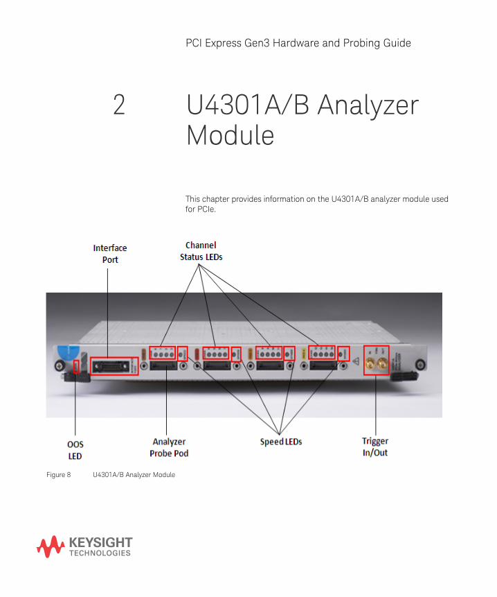
Figure 8 U4301A/B Analyzer Module
30 PCI Express Gen3 Hardware and Probing Guide
2 U4301A/B Analyzer Module
As shown in Figure 8, the U4301A/B analyzer module has the following components:
Component Description
OOS (Out of Service) LED Indicates the power-ready status of the U4301A/B module. This LED turns red during the power-on-self-test execution on the chassis bootup. The LED then dims and finally turns off when the U4301A/B module is in a power-ready status. The LED turns red again only when a power fault condition occurs for the module.• Red, steady - If the LED remains red and does not turn off, then it indicates a
power fault condition. In such a situation, the module may require repair/service. Contact your Keysight representative to replace or service the module.
• Off - This indicates that the module has detected no power failures and is in a power-ready status.
Interface Port This component is used to share information with another U4301A/B analyzer module in the same chassis. The features of this component are not yet supported.
Pods 1-4 The module has four Pod inputs labelled as Pod 1-4 in different colors. You use these pod inputs to connect the U4301A/B module to probes to create a unidirectional (upstream or downstream and upto x16) or a bidirectional (upto x8) setup.

PCI Express Gen3 Hardware and Probing Guide 31
U4301A/B Analyzer Module 2
Channel Status LEDs Each pod input on the module provides four channels. For each of these channels, a channel status LED is provided making it a total of 16 channel LEDs on the module. These 16 LEDs, labeled 0 to 15, are used to indicate the status of each channel. The following color coding is used for these LEDs to indicate the channel status.• Red - This means that there are no signals or the lane is electrically idle.• Bl inking Red - This means that there is no frame sync on the lane.• Orange - This means that the data on the lane is not de-skewed. • Green - This means that the data on the lane is de-skewed.• Off - This means that the lane is not configured. Based on the link width that
you select in the U4301 Connection Setup tab of the Logic Analyzer GUI, the number of lanes on the U4301 module are used. The LEDs of only the used lanes glow. For example, if you are using the x4 link width, then the LEDs of only four channels will glow and the rest of the LEDs will be off.
Speed LEDs Each pod has a speed LED making it a total of four speed LEDs for a U4301A/B Analyzer module. These LEDs indicate the link speed associated with the pod channels. Out of these four speed LEDs, the speed LED of only that pod glows on which the logical lane 0 is present. The remaining three speed LEDs will be off. In case of a x8 bidirectional configuration of a U4301A/B module, the speed LEDs of only those two pods glow on which the logical lane 0 is present for upstream and downstream directions. The remaining two speed LEDs will be off. For instance, if pod1 has logical lane 0 for the upstream direction and pod3 has logical lane 0 for the downstream direction, then the speed LEDs of only these two pods will glow.The following color coding is used to interpret the status of the speed LED of the pod on which the logical lane 0 is present. • Off - This means that the system is not configured.• Red - This means that the link speed is not detected or not configured.• Yellow - This means that the link speed is 2.5 Gb/s.• Green - This means that the link speed is 5 Gb/s.• Blue - This means that the link speed is 8 Gb/s.If you selected a fixed speed (Gen1, Gen2, or Gen3) for U4301A/B in the Capture setup tab of the Logic Analyzer GUI, then the speed LED will glow according to the selected speed. If you selected the Auto speed option, then the speed LED will glow according to the detected speed.
Component Description

32 PCI Express Gen3 Hardware and Probing Guide
2 U4301A/B Analyzer Module
Trigger In/Out These connectors are used to listen to an external trigger in from a device or to send an external trigger out to another device. However, these connectors on the U4301A/B module are not currently functional. Instead of using these connectors, you can use the Trigger In/Out connectors located on the Embedded System Module (ESM) of the Keysight AXIe chassis to send or receive external trigger in and out events.The following are some important points about the Trigger In/Out connectors:• The Trigger In connector of the AXIe chassis has an adjustable threshold input
of +/-5V range and 250 mV minimum swing.• The Trigger Out connector of the AXIe chassis extends the parallel trigger bus
to external instruments. The trigger out characteristics are 3.3V CMOS, 50W line drive, and 3-state.
• Maximum trigger input voltage should not exceed 3.3 V.• Trigger Out and 10 MHz Out have nominal output level of 2.0 V with 20 ns
minimum pulse width.• Minimum Trigger In duration is 20 ns.
Component Description
WARNINGDo not directly touch any component on the analyzer module. It may be hot.
CAUTIONComponents on the analyzer module are sensitive to the static electricity. Therefore, take necessary anti-static precautions, such as wear a grounded wrist strap, to minimize the possibility of electrostatic damage.

PCI Express Gen3 Hardware and Probing Guide
3 U4321A Solid Slot In-terposer Card
U4321A Solid Slot Interposer Description / 34 Setting up a bidirectional (x1-x8) configuration using a U4321A SSI Card / 40 Setting up a unidirectional (x1-x16) configuration using a U4321A SSI Card / 43 Setting up a x16 upstream and downstream configuration using a U4321A SSI Card / 48 U4321A Solid Slot Interposer Dimensions / 50
This chapter provides information on the U4321A solid slot interposer card used for PCIe Gen3.

34 PCI Express Gen3 Hardware and Probing Guide
3 U4321A Solid Slot Interposer Card
U4321A Solid Slot Interposer Description
The U4321A solid slot interposer card comes in four form factors: x1, x4, x8, and x16 link width.
The following figures show the U4321A solid slot interposer card for the x16 link width.
Figure 9 U4321A Solid Slot Interposer Card (primary side)
PCI Express Gen3 Hardware and Probing Guide 35
U4321A Solid Slot Interposer Card 3
Components shown in the above figure are described below:
• Add-in Card Connector— This component is used to connect any add-in PCIe card at the top of the U4321A solid slot interposer.
• Edge Connector— This component is used to connect U4321A solid slot interposer with a PCIe Connector on the backplane board or with a system.
This component comes with a protective foam cover to protect it from electrostatic damage.
Figure 10 U4321A Solid Slot Interposer Card (secondary side)
Add-in Card ConnectorEdge Connector Heat Protection Cover
Reset ButtonHeat SinkPower
SupplyConnector

36 PCI Express Gen3 Hardware and Probing Guide
3 U4321A Solid Slot Interposer Card
Figure 11 Protective Foam Cover for Edge Connector
• Ports— The U4321A solid slot interposer has the following ports:
• Port A — This port is for lanes 0-7, upstream.
• Port B — This port is for lanes 8-15, upstream.
• Port C — This port is for lanes 8-15, downstream.
• Port D — This port is for lanes 0-7, downstream.
If you use the U4321A solid slot interposer for x1, x4, or x8 link widths, Ports B and C are not available.
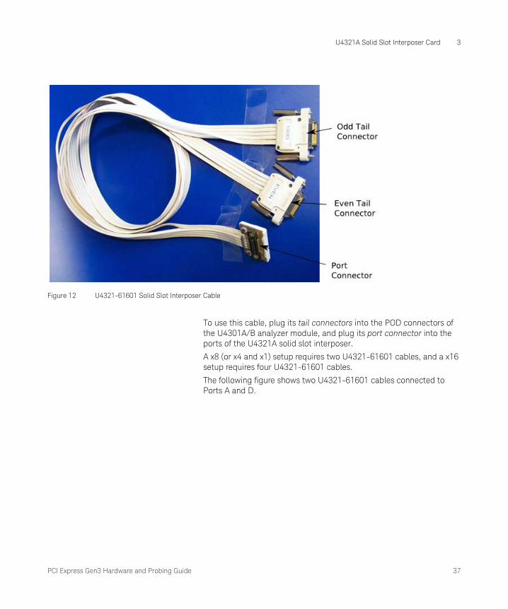
• Cables— These are the U4321-61601 Solid Slot Interposer cables that connect the U4301A/B PCIe 8Gb/s analyzer module to the U4321A solid slot interposer.
The following figure shows one U4321-61601 cable.
NOTEPlease remove the protective foam cover before using the card, and attach it again when the card is not in use.
PCI Express Gen3 Hardware and Probing Guide 37
U4321A Solid Slot Interposer Card 3
To use this cable, plug its tail connectors into the POD connectors of the U4301A/B analyzer module, and plug its port connector into the ports of the U4321A solid slot interposer.
A x8 (or x4 and x1) setup requires two U4321-61601 cables, and a x16 setup requires four U4321-61601 cables.
The following figure shows two U4321-61601 cables connected to Ports A and D.
Figure 12 U4321-61601 Solid Slot Interposer Cable

38 PCI Express Gen3 Hardware and Probing Guide
3 U4321A Solid Slot Interposer Card
Figure 13 U4321A Solid Slot Interposer Card with attached cables for x8 link width
The following figure shows four U4321-61601 cables connected to all the four ports.
Figure 14 U4321A Solid Slot Interposer Card with attached cables for x16 link width
PCI Express Gen3 Hardware and Probing Guide 39
U4321A Solid Slot Interposer Card 3
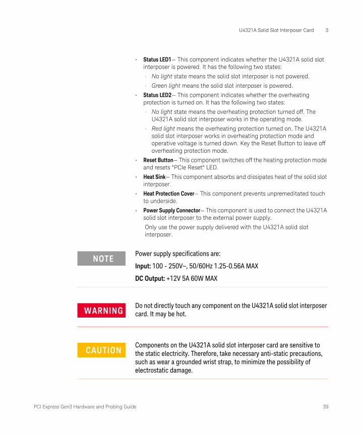
• Status LED1— This component indicates whether the U4321A solid slot interposer is powered. It has the following two states:
• No light state means the solid slot interposer is not powered.
• Green light means the solid slot interposer is powered.
• Status LED2— This component indicates whether the overheating protection is turned on. It has the following two states:
• No light state means the overheating protection turned off. The U4321A solid slot interposer works in the operating mode.
• Red light means the overheating protection turned on. The U4321A solid slot interposer works in overheating protection mode and operative voltage is turned down. Key the Reset Button to leave off overheating protection mode.
• Reset Button— This component switches off the heating protection mode and resets "PCIe Reset" LED.
• Heat Sink— This component absorbs and dissipates heat of the solid slot interposer.
• Heat Protection Cover— This component prevents unpremeditated touch to underside.
• Power Supply Connector— This component is used to connect the U4321A solid slot interposer to the external power supply.
Only use the power supply delivered with the U4321A solid slot interposer.
NOTEPower supply specifications are:
Input: 100 - 250V~, 50/60Hz 1.25-0.56A MAX
DC Output: +12V 5A 60W MAX
WARNINGDo not directly touch any component on the U4321A solid slot interposer card. It may be hot.
CAUTIONComponents on the U4321A solid slot interposer card are sensitive to the static electricity. Therefore, take necessary anti-static precautions, such as wear a grounded wrist strap, to minimize the possibility of electrostatic damage.

40 PCI Express Gen3 Hardware and Probing Guide
3 U4321A Solid Slot Interposer Card
Setting up a bidirectional (x1-x8) configuration using a U4321A SSI Card
For a x8 bidirectional configuration
You need a single U4301A/B Analyzer module and a U4321A SSI card with two U4321-61601 cables for a x8 bidirectional setup.
Perform the following steps for a x8 bidirectional hardware and probing setup.
1 Plug the port connector of the first U4321-61601 cable into the upstream Port A of the U4321A solid slot interposer.
2 Plug the tail connectors of the first U4321-61601 cable into the POD connectors of Pod 1 and 2 of the U4301A/B Analyzer module.
3 Plug the port connector of the second U4321-61601 cable into the downstream Port D of the U4321A solid slot interposer.
4 Plug the tail connectors of the second U4321-61601 cable into the POD connectors of Pod 3 and 4 of the same U4301A/B analyzer module.
The following figure illustrates a x8 bidirectional setup when a single U4301A/B module is used to probe and capture data in downstream as well as upstream directions.

PCI Express Gen3 Hardware and Probing Guide 41
U4321A Solid Slot Interposer Card 3
Figure 15 x8 bidirectional setup using a U4321A solid slot interposer card and a single U4301A/B module

42 PCI Express Gen3 Hardware and Probing Guide
3 U4321A Solid Slot Interposer Card
For a x1, x2, or x4 bidirectional configuration
For a x1, x2, or x4 bidirectional setup, you need the same hardware and probing setup as described above for a x8 bidirectional setup. The only difference would be that you need to plug the tail connectors of the:
• first U4321-61601 cable into the POD connector of Pod 2 of the U4301A/B Analyzer module.
• second U4321-61601 cable into the POD connector of Pod 4 of the U4301A/B Analyzer module.

PCI Express Gen3 Hardware and Probing Guide 43
U4321A Solid Slot Interposer Card 3
Setting up a unidirectional (x1-x16) configuration using a U4321A SSI Card
For a x16 downstream configuration
You need a single U4301A/B Analyzer module and a U4321A SSI card with two U4321-61601 cables for a x16 downstream setup.
Perform the following steps for a x16 downstream hardware and probing setup.
1 Plug the port connector of the first U4321-61601 cable into Port D of the U4321A solid slot interposer.
2 Plug the port connector of the second U4321-61601 cable into Port C of the U4321A solid slot interposer.
3 Plug the tail connectors of the first U4321-61601 cable into POD 1 and 2 of the U4301A/B analyzer module.
4 Plug the tail connectors of the second U4321-61601 cable into POD 3 and 4 of the U4301A/B analyzer module.
The upstream ports A and B of the U4321A SSI card will not be utilized in this setup.
The following figure illustrates a x16 downstream setup.

44 PCI Express Gen3 Hardware and Probing Guide
3 U4321A Solid Slot Interposer Card
Figure 16 x16 downstream setup using a U4321A Slot Interposer card and a U4301A/B module

PCI Express Gen3 Hardware and Probing Guide 45
U4321A Solid Slot Interposer Card 3
For a x1, x2, x4, or x8 downstream configuration
For a x1, x2, x4, or x8 downstream setup, you need a a single U4301A/B Analyzer module, a U4321A SSI card, and a U4321-61601 cable. For these setups, follow the same steps as described above for a x16 downstream setup except with the following differences:
• you would use only Port D of the SSI card
• you would use Pod 1 and 2 of the U4301A/B module (in case of a x8 setup) and Pod 2 of the U4301A/B module (in case of a x1, x2, or x4 setup).
For a x16 upstream configuration
You need a single U4301A/B Analyzer module and a U4321A SSI card with two U4321-61601 cables for a x16 upstream setup.
Perform the following steps for a x16 upstream hardware and probing setup.
1 Plug the port connector of the first U4321-61601 cable into Port A of the U4321A solid slot interposer.
2 Plug the port connector of the second U4321-61601 cable into Port B of the U4321A solid slot interposer.
3 Plug the tail connectors of the first U4321-61601 cable into POD 1 and 2 of the U4301A/B analyzer module.
4 Plug the tail connectors of the second U4321-61601 cable into POD 3 and 4 of the U4301A/B analyzer module.
The downstream ports C and D of the U4321A SSI card will not be utilized in this setup.
The following figure illustrates a x16 upstream setup.

46 PCI Express Gen3 Hardware and Probing Guide
3 U4321A Solid Slot Interposer Card
Figure 17 x16 upstream setup using a U4321A Slot Interposer card and a U4301A/B module

PCI Express Gen3 Hardware and Probing Guide 47
U4321A Solid Slot Interposer Card 3
For a x1, x2, x4, or x8 upstream configuration
For a x1, x2, x4, or x8 upstream setup, you need a a single U4301A/B Analyzer module, a U4321A SSI card, and a U4321-61601 cable. For these setups, follow the same steps as described above for a x16 upstream setup except with the following differences:
• you would use only Port A of the SSI card
• you would use Pod 1 and 2 of the U4301A/B module (in case of a x8 setup) and Pod 2 of the U4301A/B module (in case of a x1, x2, or x4 setup).

48 PCI Express Gen3 Hardware and Probing Guide
3 U4321A Solid Slot Interposer Card
Setting up a x16 upstream and downstream configuration using a U4321A SSI Card
If you want to probe and capture upstream as well downstream data with x16 link width, you need two U4301A/B Analyzer modules, a U4321A SSI card and four U4321-61601 cables.
Perform the following steps for a x16 upstream and downstream hardware and probing setup.
Upstream setup
1 Plug the port connector of the first U4321-61601 cable into Port A of the U4321A solid slot interposer.
2 Plug the port connector of the second U4321-61601 cable into Port B of the U4321A solid slot interposer.
3 Plug the tail connectors of the first U4321-61601 cable into POD 1 and 2 of the U4301A/B analyzer module that you selected for the upstream setup.
4 Plug the tail connectors of the second U4321-61601 cable into POD 3 and 4 of the U4301A/B analyzer module that you selected for the upstream setup.
Downstream setup
1 Plug the port connector of the third U4321-61601 cable into Port D of the U4321A solid slot interposer.
2 Plug the port connector of the fourth U4321-61601 cable into Port C of the U4321A solid slot interposer.
3 Plug the tail connectors of the third U4321-61601 cable into POD 1 and 2 of the U4301A/B analyzer module that you selected for the downstream setup.
4 Plug the tail connectors of the fourth U4321-61601 cable into POD 3 and 4 of the U4301A/B analyzer module that you selected for the downstream setup.
The following figure illustrates a x16 upstream and downstream setup.

PCI Express Gen3 Hardware and Probing Guide 49
U4321A Solid Slot Interposer Card 3
Figure 18 x16 upstream and downstream setup using a U4321A Slot Interposer card and two U4301A/B modules
50 PCI Express Gen3 Hardware and Probing Guide
3 U4321A Solid Slot Interposer Card
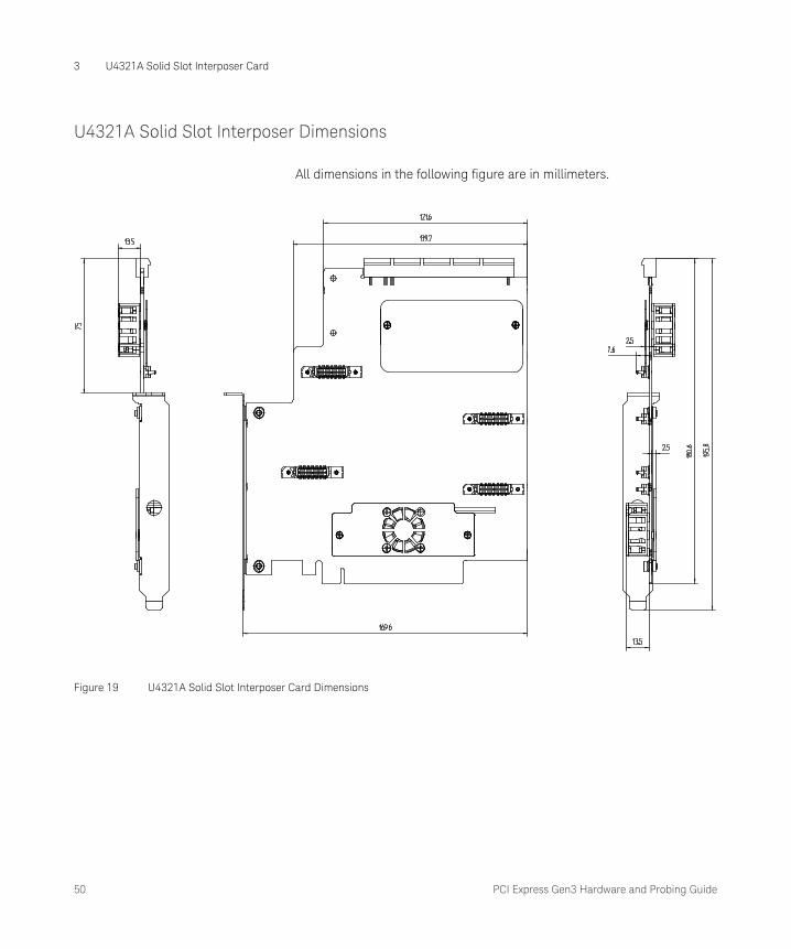
U4321A Solid Slot Interposer Dimensions
All dimensions in the following figure are in millimeters.
Figure 19 U4321A Solid Slot Interposer Card Dimensions

PCI Express Gen3 Hardware and Probing Guide
4 Soft Touch Midbus 3.0 Probes
DUT Mechanical Design Considerations / 54 DUT Electrical Design Considerations / 60 Supported Footprint Pinouts and Pod Connections / 64 Probe Installation Instructions / 93 Probe Characteristics / 97
The Keysight midbus 3.0 series of probes using soft touch technology are specially designed to provide support for up to 16 channel probing solutions.
To integrate a midbus probe, a midbus probe footprint must be designed into the device under test (DUT).
A 3-pin header must also be designed into the DUT if it needs to supply a reference clock to the protocol analyzer.
This chapter is intended to provide information needed by platform and system design teams for integration of midbus 3.0 probes into their designs. It provides a mechanical and electrical solution space for Midbus Probe placement with the PCI Express bus.
Although information on PCI Express topology and specifications will be given, this information is not intended to take the place of other PCI Express design documentation. It is assumed that a design team utilizing this document for their design constraints will validate their designs through pre- and post-route electrical simulation and keep-out volume analysis.
Nomenclature • U4322A refers to midbus 3.0 probe.
52 PCI Express Gen3 Hardware and Probing Guide
4 Soft Touch Midbus 3.0 Probes
• Midbus connection, midbus probe, and midbus footprint refer to the Keysight midbus 3.0 footprint connector (U4322A) PCI Express compression cable set.
• "channel" refers to either an upstream differential pair OR downstream differential pair for a given lane. In other words, a "channel" refers to either a transmit-differential pair OR a receive-differential pair for a given lane.
Link Configuration Support The midbus 3.0 offers a number of different probing options for different applications. The platform designer has the flexibility to configure a probing solution that best meets the needs of the system. With midbus 3.0 offering upto 16 channel probing solutions, the following configurations may be made*:
• Upstream and downstream channels of one x8 link.
• Upstream or downstream channels of one x16 link.
• Upstream or downstream channels of up to four x4, x2, or x1 links.
*As long as the Midbus Probe placement within the system requirements are met. System designers should verify that their system requirements are supported by the midbus 3.0 by contacting Keysight Technologies directly.
Retention Modules The retention module secures the midbus probe to the device under test (DUT). To achieve this, the retention module must be bolted onto the DUT.
Note that there is a keying feature on the retention module and probe head. If the retention module alignment is off by 180 degrees, it does not work.
After the retention module is properly bolted onto the DUT, the probe can be easily plugged into the retention module (see “Probe Installation Instructions" on page 93).
One kit of 5 retention modules is supplied with each U4322A midbus probe.
Contact your local sales representative to order additional retention modules.
• Model Number: U4329A Retention modules for U4322A Mid-bus probe 3.0 for PCIe 8 Gbps – kit of 5
NOTEOther combinations may be available. Contact Keysight Technologies for the latest support configurations.

PCI Express Gen3 Hardware and Probing Guide 53
Soft Touch Midbus 3.0 Probes 4
Reference Clock Connector Midbus probes provide reference clock connections for situations where it is necessary to probe the reference clock from the device under test (DUT).
For many solution setups, an external reference clock is not required. However, if any of the following cases are true, an external reference clock must be supplied for each PCI Express clock domain for which the case applies.
• When the midbus probe is used with a system that supports Spread Spectrum Clocking (SSC) on the reference clock to all the PCI Express agents and the SSC cannot be disabled
• When testing must be done with SSC enabled, because a problem does not manifest with SSC disabled.
• If the link frequency is intentionally margin tested outside the standard ±300 ppm tolerance.
The reference clock can be a dedicated clock, in which case appropriate terminators must be provided on the board. Alternately, the signals may be a tap off an existing clock, since the probes are designed to not significantly load the signals. Note that if the reference clock signal is series/source terminated then the position of the tap point must be at the far end of the line. However, this needs to be verified by the system platform designers to verify proper functionality. See reference clock model for more information.
See Also • “Footprint for Reference Clock Connector" on page 58
• “Keep-Out Volume for Reference Clock Connector" on page 58
• “Electrical Requirements for Reference Clock Connector" on page 63
• “Load Model for Reference Clock Connector" on page 63
NOTEThis is more restrictive than the PCI Express standard of ±300 ppm, but must be considered. For more information, contact Keysight Technologies directly.

54 PCI Express Gen3 Hardware and Probing Guide
4 Soft Touch Midbus 3.0 Probes
DUT Mechanical Design Considerations
• “Footprint for Probe" on page 54
• “Keep-Out Volume for Probe and Retention Module Dimensions" on page 57
• “Footprint for Reference Clock Connector" on page 58
• “Keep-Out Volume for Reference Clock Connector" on page 58
Footprint for Probe
The Midbus probe 3.0 footprint that needs to be designed into the device under test can be observed in the following figure which shows the detailed layout dimensions. Notice that the connector has 41 pins.

PCI Express Gen3 Hardware and Probing Guide 55
Soft Touch Midbus 3.0 Probes 4
Figure 20 Midbus 3.0 Footprint Dimensions, Pin Numbering, and Specification

56 PCI Express Gen3 Hardware and Probing Guide
4 Soft Touch Midbus 3.0 Probes
Notes:
1 All dimensions are in inches.
2 Solder mask must not extend above the pad height for a distance of 0.005 inches from the pad.
3 Via-in-pad is allowed if the vias are filled level with the pad or the via hole size is less than 0.005 inches.
4 Permissible surface finishes on the pads are HASL, immersion silver, or gold over nickel. The height of the pads contacted by the probe must be within +/- 0.007 inches of the bottom surface of the retention module.
The following figure shows the detailed view of a pad with geometrical information on it.
Figure 21 Detail A - Detailed View of a Pad

PCI Express Gen3 Hardware and Probing Guide 57
Soft Touch Midbus 3.0 Probes 4
Keep-Out Volume for Probe and Retention Module Dimensions
Notes:
1 All dimensions are in inches.
2 See the footprint drawing (“Footprint for Probe" on page 54) for dimensions and details that include hole locations.
Figure 22 Midbus 3.0 Probe Keep-Out Volume

58 PCI Express Gen3 Hardware and Probing Guide
4 Soft Touch Midbus 3.0 Probes
Footprint for Reference Clock Connector
A 3-pin header (1 by 3, 0.05 inch center spacing) will provide the connection for reference clock to the midbus. A small high impedance clock probe will connect to this header to the midbus. Note that an individual reference clock header is required for each PCI Express clock domain on the system.
The following are recommended part numbers for through-hole and surface mount versions of the 3-pin header for reference clock:
• Through-hole:
Samtec* TMS-103-02-S-S
• Surface mount:
Samtec* FTR-103-02-S-S
See Also • “Keep-Out Volume for Reference Clock Connector" on page 58
Keep-Out Volume for Reference Clock Connector
Keep-out volumes for the reference clock probes are given in the following figure. The pin headers reside symmetrically within the keep-out volume on the device under test. For more specific information on keep-out volumes for particular solutions please contact Keysight Technologies.
Signal Pin Number
REFCLKp 1 (or 3)*
GND or N/C 2
REFCLKn 3 (or 1)*
* The probe can be plugged onto the pin header in either orientation.

PCI Express Gen3 Hardware and Probing Guide 59
Soft Touch Midbus 3.0 Probes 4
Figure 23 Reference clock probe keep-out volume

60 PCI Express Gen3 Hardware and Probing Guide
4 Soft Touch Midbus 3.0 Probes
DUT Electrical Design Considerations
• “Routing Considerations" on page 60
• “Load Model for Probe" on page 62
• “Electrical Requirements for Reference Clock Connector" on page 63
• “Load Model for Reference Clock Connector" on page 63
Routing Considerations
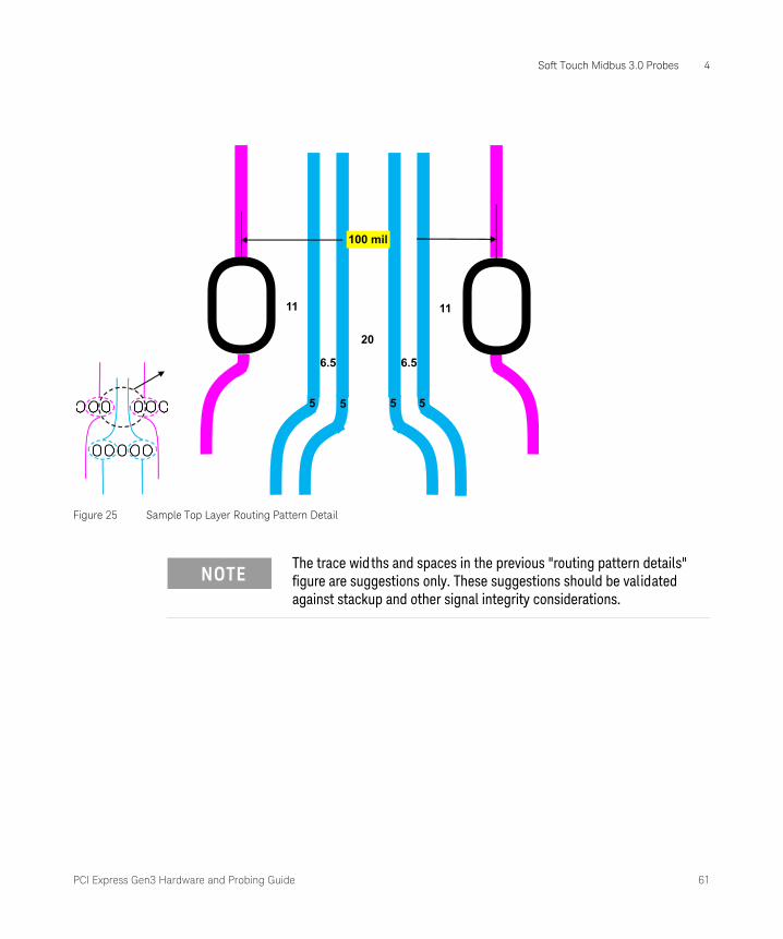
Figure 24 Sample Top Layer Routing Pattern
PCI Express Gen3 Hardware and Probing Guide 61
Soft Touch Midbus 3.0 Probes 4
Figure 25 Sample Top Layer Routing Pattern Detail
11
20
6.5 6.5
100 mil
11
5 5 5 5
NOTEThe trace widths and spaces in the previous "routing pattern details" figure are suggestions only. These suggestions should be validated against stackup and other signal integrity considerations.

62 PCI Express Gen3 Hardware and Probing Guide
4 Soft Touch Midbus 3.0 Probes
Load Model for Probe
Figure 26 Load Model for Midbus 3.0 Probe
For PCI Express Gen3, it is not meaningful to talk about eye openings as an input requirement to a receiver, because for Gen3 you are dealing with a closed eye. In this consideration, PCI Express Gen3 compliant receivers are required to have equalization capabilities, and the Equalizing Snoop Probe is no different in this regard. In fact, the Equalizing Snoop Probe has a wide range of equalization capabilities in its receiver — a range that is too extensive to attempt to enumerate in a model.
The good news is that the PCI Express 3.0 specification takes this into account already in its Receiver Compliance testing section of the PCI Express Gen3 Specification (sections 4.3.4.3.2 and sections 4.3.6.4 referring to spec version 0.9), and the Equalizing Snoop Probe passes this testing. The way to evaluate this is to run the traditional channel simulation with the provided load model, and evaluate the signal at the probe tip using the method described in the receiver compliance testing section (that is, section 4.3.4.4). If the eye present at the probe tip is at least the size of the stressed eye specification (after performing the appropriate post-processing), then you can be assured of reliable data capture. PCI-SIG also provides a freely-available tool that supports the
260 Ohms
1000 pF
110 fF
1000 pF
260 Ohms
105 fF
105 fFCH_x_P
CH_x_NInputs

PCI Express Gen3 Hardware and Probing Guide 63
Soft Touch Midbus 3.0 Probes 4
post processing steps required. See "http://www.pcisig.com/specifications/pciexpress/base2/seasim_package/" at "www.pcisig.org".
Electrical Requirements for Reference Clock Connector
If reference clock tolerance is less than ±300 ppm, there is no need for providing reference to the probe. If the reference clock tolerance is greater than ±300 ppm, there is a need for providing reference (SSC) to the probe.
See Also • “Load Model for Reference Clock Connector" on page 63
Load Model for Reference Clock Connector
Load models for the reference clock probe are given in this section. System designers are expected to perform simulations of the reference clock networks with the header and midbus load models to ensure good signal integrity of the reference clocks at the header to the midbus. The pin header parasitics may be obtained from the connector vendor.
Figure 27 Reference clock probe load model
Midbus Requirement Symbol Min. Max. Comments
Differential voltage at ref clock attach point
Vppdiff 0.8 V 2 V Vppdiff = |2*(Vrefclockp – Vrefclockn)|
Reference clock frequency without SSC
f 100 MHz -300 ppm 100 MHz +300 ppm
Reference clock frequency with SSC
f 100 MHz -0.5% 100 MHz +0%

64 PCI Express Gen3 Hardware and Probing Guide
4 Soft Touch Midbus 3.0 Probes
Supported Footprint Pinouts and Pod Connections
The pod connection pictures that appear in the following footprint descriptions also appear as "Connection diagrams" in the Keysight Logic and Protocol Analyzer application's Setup dialog for the PCIe analyzer module.
x16 Straight Footprint
One bidirectional x16 link in two unidirectional full-width PCI Express midbus probe footprints pinout.
Supported Footprint Configuration Probe Required Number of U4301A/B Protocol Analyzer Modules Required
“x16 Straight Footprint" on page 64 2 x Full Size Mid-Bus (U4322A) 2
“x16 Swizzled Footprint" on page 67 2 x Full Size Mid-Bus (U4322A) 2
“x16 Unidirectional Footprint" on page 70 1 x Full Size Mid-Bus (U4322A) 1
“x8 Bidirectional Footprint" on page 72 1 x Full Size Mid-Bus (U4322A) 1
“Two x8 Unidirectional Footprint" on page 74 1 x Full Size Mid-Bus (U4322A) 2
“Two x4 Bidirectional Footprint" on page 76 1 x Full Size Mid-Bus (U4322A) 2
“x4 Bidirectional Footprint" on page 78 1 x Full Size Mid-Bus (U4322A) 1
“Two x4 Unidirectional Footprint" on page 80 1 x Full Size Mid-Bus (U4322A) 2
“Two x2 Bidirectional Footprint" on page 83 1 x Full Size Mid-Bus (U4322A) 2
“Two x2 Unidirectional Footprint" on page 85 1 x Full Size Mid-Bus (U4322A) 2
“x1 Bi-directional Footprint" on page 87 1 x Full Size Mid-Bus (U4322A) 1
“Two x1 Bidirectional Footprint" on page 89 1 x Full Size Mid-Bus (U4322A) 2
“Two x1 Unidirectional Footprint" on page 91 1 x Full Size Mid-Bus (U4322A) 2

PCI Express Gen3 Hardware and Probing Guide 65
Soft Touch Midbus 3.0 Probes 4
Module 1 Module 2
Signal Name
Pin # Pin # Signal Name
Signal Name
Pin # Pin # Signal Name
C1 GND C1 GND
up1p B1 C2 up0p down1p B1 C2 down0p
up1n B2 C3 up0n down1n B2 C3 down0n
GND B3 GND B3
up2p B4 C4 up3p down2p B4 C4 down3p
up2n B5 C5 up3n down2n B5 C5 down3n
C6 GND C6 GND
up5p B6 C7 up4p down5p B6 C7 down4p
up5n B7 C8 up4n down5n B7 C8 down4n
GND B8 GND B8
up6p B9 C9 up7p down6p B9 C9 down7p
up6n B10 C10 up7n down6n B10 C10 down7n
C11 GND C11 GND
up9p B11 C12 up8p down9p B11 C12 down8p
up9n B12 C13 up8n down9n B12 C13 down8n
GND B13 GND B13
up10p B14 C14 up11p down10p B14 C14 down11p
up10n B15 C15 up11n down10n B15 C15 down11n
C16 GND C16 GND
up13p B16 C17 up12p down13p B16 C17 down12p
up13n B17 C18 up12n down13n B17 C18 down12n
GND B18 GND B18
up14p B19 C19 up15p down14p B19 C19 down15p
up14n B20 C20 up15n down14n B20 C20 down15n
C21 GND C21 GND

66 PCI Express Gen3 Hardware and Probing Guide
4 Soft Touch Midbus 3.0 Probes
Figure 28 x16 Straight Footprint Pod Connection

PCI Express Gen3 Hardware and Probing Guide 67
Soft Touch Midbus 3.0 Probes 4
x16 Swizzled Footprint
One bidirectional x16 link in two bidirectional full-width PCI Express midbus probe footprints pinout.

68 PCI Express Gen3 Hardware and Probing Guide
4 Soft Touch Midbus 3.0 Probes
Downstream Module 1 Upstream Module 2 Downstream Module 1 Upstream Module 2
Signal Name
Pin # Pin # Signal Name
Signal Name
Pin # Pin # Signal Name
C1 GND C1 GND
down0p B1 C2 up0p down8p B1 C2 up8p
down0n B2 C3 up0n down8n B2 C3 up8n
GND B3 GND B3
down1p B4 C4 up1p down9p B4 C4 up9p
down1n B5 C5 up1n down9n B5 C5 up9n
C6 GND C6 GND
down2p B6 C7 up2p down10p B6 C7 up10p
down2n B7 C8 up2n down10n B7 C8 up10n
GND B8 GND B8
down3p B9 C9 up3p down11p B9 C9 up11p
down3n B10 C10 up3n down11n B10 C10 up11n
C11 GND C11 GND
down4p B11 C12 up4p down12p B11 C12 up12p
down4n B12 C13 up4n down12n B12 C13 up12n
GND B13 GND B13
down5p B14 C14 up5p down13p B14 C14 up13p
down5n B15 C15 up5n down13n B15 C15 up13n
C16 GND C16 GND
down6p B16 C17 up6p down14p B16 C17 up14p
down6n B17 C18 up6n down14n B17 C18 up14n
GND B18 GND B18
down7p B19 C19 up7p down15p B19 C19 up15p
down7n B20 C20 up7n down15n B20 C20 up15n
C21 GND C21 GND

PCI Express Gen3 Hardware and Probing Guide 69
Soft Touch Midbus 3.0 Probes 4
Figure 29 x16 Swizzled Footprint Pod Connection

70 PCI Express Gen3 Hardware and Probing Guide
4 Soft Touch Midbus 3.0 Probes
x16 Unidirectional Footprint
One x16 unidirectional specific 16 channel PCI Express.
Module 1
Signal Name Pin # Pin # Signal Name
C1 GND
lane1p B1 C2 lane0p
lane1n B2 C3 lane0n
GND B3
lane2p B4 C4 lane3p
lane2n B5 C5 lane3n
C6 GND
lane5p B6 C7 lane4p
lane5n B7 C8 lane4n
GND B8
lane6p B9 C9 lane7p
lane6n B10 C10 lane7n
C11 GND
lane9p B11 C12 lane8p
lane9n B12 C13 lane8n
GND B13
lane10p B14 C14 lane11p
lane10n B15 C15 lane11n
C16 GND
lane13p B16 C17 lane12p
lane13n B17 C18 lane12n
GND B18
lane14p B19 C19 lane15p
lane14n B20 C20 lane15n
C21 GND

PCI Express Gen3 Hardware and Probing Guide 71
Soft Touch Midbus 3.0 Probes 4
Figure 30 x16 Unidirectional Footprint Pod Connection

72 PCI Express Gen3 Hardware and Probing Guide
4 Soft Touch Midbus 3.0 Probes
x8 Bidirectional Footprint
You can use a single U4301A/B module with a Midbus 3.0 probe to create a x8 bidirectional setup.
One x8 bidirectional specific 16 channel PCI Express
Module 1
Signal Name Pin # Pin # Signal Name
C1 GND
down0p B1 C2 up0p
down0n B2 C3 up0n
GND B3
down1p B4 C4 up1p
down1n B5 C5 up1n
C6 GND
down2p B6 C7 up2p
down2n B7 C8 up2n
GND B8
down3p B9 C9 up3p
down3n B10 C10 up3n
C11 GND
down4p B11 C12 up4p
down4n B12 C13 up4n
GND B13
down5p B14 C14 up5p
down5n B15 C15 up5n
C16 GND
down6p B16 C17 up6p
down6n B17 C18 up6n
GND B18
down7p B19 C19 up7p
down7p B20 C20 up7p
C21 GND

PCI Express Gen3 Hardware and Probing Guide 73
Soft Touch Midbus 3.0 Probes 4
Figure 31 x8 Bidirectional Footprint Pod Connection when a single U4301A/B module is used
74 PCI Express Gen3 Hardware and Probing Guide
4 Soft Touch Midbus 3.0 Probes
Two x8 Unidirectional Footprint
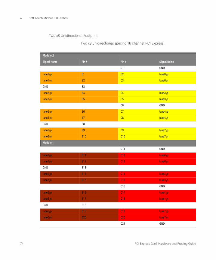
Two x8 unidirectional specific 16 channel PCI Express.
Module 2
Signal Name Pin # Pin # Signal Name
C1 GND
lane11p B1 C2 lane01p
lane11n B2 C3 lane01n
GND B3
lane21p B4 C4 lane31p
lane21n B5 C5 lane31n
C6 GND
lane51p B6 C7 lane41p
lane51n B7 C8 lane41n
GND B8
lane61p B9 C9 lane71p
lane61n B10 C10 lane71n
Module 1
C11 GND
lane12p B11 C12 lane02p
lane12n B12 C13 lane02n
GND B13
lane22p B14 C14 lane32p
lane22n B15 C15 lane32n
C16 GND
lane52p B16 C17 lane42p
lane52n B17 C18 lane42n
GND B18
lane62p B19 C19 lane72p
lane62n B20 C20 lane72n
C21 GND

PCI Express Gen3 Hardware and Probing Guide 75
Soft Touch Midbus 3.0 Probes 4
Figure 32 Two x8 Unidirectional Footprint Pod Connection

76 PCI Express Gen3 Hardware and Probing Guide
4 Soft Touch Midbus 3.0 Probes
Two x4 Bidirectional Footprint
Two x4 bidirectional specific 16 channel PCI Express.
Module 2
Signal Name Pin # Pin # Signal Name
C1 GND
down01p B1 C2 up01p
down01n B2 C3 up01n
GND B3
down11p B4 C4 up11p
down11n B5 C5 up11n
C6 GND
down21p B6 C7 up21p
down21n B7 C8 up21n
GND B8
down31p B9 C9 up31p
down31n B10 C10 up31n
Module 1
C11 GND
down02p B11 C12 up02p
down02n B12 C13 up02n
GND B13
down12p B14 C14 up12p
down12n B15 C15 up12n
C16 GND
down22p B16 C17 up22p
down22n B17 C18 up22n
GND B18
down32p B19 C19 up32p
down32n B20 C20 up32n
C21 GND

PCI Express Gen3 Hardware and Probing Guide 77
Soft Touch Midbus 3.0 Probes 4
Figure 33 Two x4 Bidirectional Footprint Pod Connection

78 PCI Express Gen3 Hardware and Probing Guide
4 Soft Touch Midbus 3.0 Probes
x4 Bidirectional Footprint
You can use a single U4301A/B module with a Midbus 3.0 probe to create a x4 bidirectional setup.
One x4 bidirectional specific 16 channel PCI Express.
Module1
Signal Name Pin # Pin # Signal Name
C1 GND
down0p B1 C2 up0p
down0n B2 C3 up0n
GND B3
down1p B4 C4 up1p
down1n B5 C5 up1n
C6 GND
down2p B6 C7 up2p
down2n B7 C8 up2n
GND B8
down3p B9 C9 up3p
down3n B10 C10 up3n
C11 GND
NC B11 C12 NC
NC B12 C13 NC
GND B13
NC B14 C14 NC
NC B15 C15 NC
C16 GND
NC B16 C17 NC
NC B17 C18 NC
GND B18
NC B19 C19 NC
NC B20 C20 NC
C21 GND

PCI Express Gen3 Hardware and Probing Guide 79
Soft Touch Midbus 3.0 Probes 4
Figure 34 x4 Bidirectional Footprint Pod Connection

80 PCI Express Gen3 Hardware and Probing Guide
4 Soft Touch Midbus 3.0 Probes
Two x4 Unidirectional Footprint
Figure 35 x4 Bidirectional Footprint Pod Connection

PCI Express Gen3 Hardware and Probing Guide 81
Soft Touch Midbus 3.0 Probes 4
Four x4 unidirectional specific 16 channel PCI Express.
Module 2
Signal Name Pin # Pin # Signal Name
C1 GND
lane11p B1 C2 lane01p
lane11n B2 C3 lane01n
GND B3
lane21p B4 C4 lane31p
lane21n B5 C5 lane31n
C6 GND
NC B6 C7 NC
NC B7 C8 NC
GND B8
NC B9 C9 NC
NC B10 C10 NC
Module 1
C11 GND
lane12p B11 C12 lane02p
lane12n B12 C13 lane02n
GND B13
lane22p B14 C14 lane32p
lane22n B15 C15 lane32n
C16 GND
NC B16 C17 NC
NC B17 C18 NC
GND B18
NC B19 C19 NC
NC B20 C20 NC
C21 GND

82 PCI Express Gen3 Hardware and Probing Guide
4 Soft Touch Midbus 3.0 Probes
Figure 36 Two x4 Unidirectional Footprint Pod Connection

PCI Express Gen3 Hardware and Probing Guide 83
Soft Touch Midbus 3.0 Probes 4
Two x2 Bidirectional Footprint
Figure 37 Two x2 bi-directional specific 16 channel PCI Express.
Module 2
Signal Name Pin # Pin # Signal Name
C1 GND
down01p B1 C2 up01p
down01n B2 C3 up01n
GND B3
down11p B4 C4 up11p
down11n B5 C5 up11n
C6 GND
NC B6 C7 NC
NC B7 C8 NC
GND B8
NC B9 C9 NC
NC B10 C10 NC
Module 1
C11 GND
down02p B11 C12 up02p
down02n B12 C13 up02n
GND B13
down12p B14 C14 up12p
down12n B15 C15 up12n
C16 GND
NC B16 C17 NC
NC B17 C18 NC
GND B18
NC B19 C19 NC
NC B20 C20 NC
C21 GND

84 PCI Express Gen3 Hardware and Probing Guide
4 Soft Touch Midbus 3.0 Probes
Figure 38 Two x2 Bidirectional Footprint Pod Connection

PCI Express Gen3 Hardware and Probing Guide 85
Soft Touch Midbus 3.0 Probes 4
Two x2 Unidirectional Footprint
Two x2 unidirectional specific 16 channel PCI Express.
Module 2
Signal Name Pin # Pin # Signal Name
C1 GND
lane11p B1 C2 lane01p
lane11n B2 C3 lane01n
GND B3
NC B4 C4 NC
NC B5 C5 NC
C6 GND
NC B6 C7 NC
NC B7 C8 NC
GND B8
NC B9 C9 NC
NC B10 C10 NC
Module 1
C11 GND
lane12p B11 C12 lane02p
lane12n B12 C13 lane02n
GND B13
NC B14 C14 NC
NC B15 C15 NC
C16 GND
NC B16 C17 NC
NC B17 C18 NC
GND B18
NC B19 C19 NC
NC B20 C20 NC
C21 GND

86 PCI Express Gen3 Hardware and Probing Guide
4 Soft Touch Midbus 3.0 Probes
Figure 39 Two x2 Unidirectional Footprint Pod Connection

PCI Express Gen3 Hardware and Probing Guide 87
Soft Touch Midbus 3.0 Probes 4
x1 Bi-directional Footprint
You can use a single U4301A/B module with a Midbus 3.0 probe to create a x1 bi-directional setup.
One x1 bi-directional specific 16 channel PCI Express.
Module 1
Signal Name Pin # Pin # Signal Name
C1 GND
down0p B1 C2 up0p
down0n B2 C3 up0n
GND B3
NC B4 C4 NC
NC B5 C5 NC
C6 GND
NC B6 C7 NC
NC B7 C8 NC
GND B8
NC B9 C9 NC
NC B10 C10 NC
C11 GND
NC B11 C12 NC
NC B12 C13 NC
GND B13
NC B14 C14 NC
NC B15 C15 NC
C16 GND
NC B16 C17 NC
NC B17 C18 NC
GND B18
NC B19 C19 NC
NC B20 C20 NC
C21 GND

88 PCI Express Gen3 Hardware and Probing Guide
4 Soft Touch Midbus 3.0 Probes
Figure 40 x1 Bidirectional Footprint Pod Connection

PCI Express Gen3 Hardware and Probing Guide 89
Soft Touch Midbus 3.0 Probes 4
Two x1 Bidirectional Footprint
Two x1 bidirectional specific 16 channel PCI Express.
3
Module 2
Signal Name Pin # Pin # Signal Name
C1 GND
down01p B1 C2 up01p
down01n B2 C3 up01n
GND B3
NC B4 C4 NC
NC B5 C5 NC
C6 GND
NC B6 C7 NC
NC B7 C8 NC
GND B8
NC B9 C9 NC
NC B10 C10 NC
Module 1
C11 GND
down02p B11 C12 up02p
down02n B12 C13 up02n
GND B13
NC B14 C14 NC
NC B15 C15 NC
C16 GND
NC B16 C17 NC
NC B17 C18 NC
GND B18
NC B19 C19 NC
NC B20 C20 NC
C21 GND

90 PCI Express Gen3 Hardware and Probing Guide
4 Soft Touch Midbus 3.0 Probes
Figure 41 Two x1 Bidirectional Footprint Pod Connection

PCI Express Gen3 Hardware and Probing Guide 91
Soft Touch Midbus 3.0 Probes 4
Two x1 Unidirectional Footprint
Two x1 unidirectional specific 16 channel PCI Express.
Module 2
Signal Name Pin # Pin # Signal Name
C1 GND
NC B1 C2 lane01p
NC B2 C3 lane01n
GND B3
NC B4 C4 NC
NC B5 C5 NC
C6 GND
NC B6 C7 NC
NC B7 C8 NC
GND B8
NC B9 C9 NC
NC B10 C10 NC
Module 1
C11 GND
NC B11 C12 lane02p
NC B12 C13 lane02n
GND B13
NC B14 C14 NC
NC B15 C15 NC
C16 GND
NC B16 C17 NC
NC B17 C18 NC
GND B18
NC B19 C19 NC
NC B20 C20 NC
C21 GND

92 PCI Express Gen3 Hardware and Probing Guide
4 Soft Touch Midbus 3.0 Probes
Figure 42 Two x1 Unidirectional Footprint Pod Connection

PCI Express Gen3 Hardware and Probing Guide 93
Soft Touch Midbus 3.0 Probes 4
Probe Installation Instructions
1 Connect the midbus 3.0 probe's pod connectors to the protocol analyzer blade.
2 There are two methods for connecting the probe head to the DUT:
• “Bolting Probe Head and Retention Module onto DUT" on page 93 — you can use this method when the bottom side of the DUT circuit board is easily accessible. This method provides extra protection for the pins on the probe head.
• “Inserting Probe Head into Retention Module on DUT" on page 95 — you can use this method in situations where the retention module is already bolted to the DUT circuit board.
3 Finally, if an external reference clock signal is to be supplied to protocol analyzer, connect the external clock cable (of the midbus) to the reference clock header on the device under test.
See Also • “Supported Footprint Pinouts and Pod Connections" on page 64
Bolting Probe Head and Retention Module onto DUT
When using this method of probe installation, the probe head is already screwed into the retention module, and together they are bolted onto the DUT circuit board.
CAUTIONOver-tightening the module connector screws can damage the probe. Because of the size of the screws, you may need to use a screwdriver; however, only tighten the screws as much as if you were finger-tightening them.

94 PCI Express Gen3 Hardware and Probing Guide
4 Soft Touch Midbus 3.0 Probes
This method of probe installation provides some extra protection for the pins on the probe head, but you must have access to the bottom side of the DUT circuit board.
1 Screw the retention module onto the probe head first.
2 Use the bolts as the alignment pins.
By doing this, the risk of dragging the probe head pins across the retention module is removed. With the bolts now being the longest feature, the pins have some protection from other components on the DUT that they could come in contact with.
3 Tighten the thumb nuts onto the back side.

PCI Express Gen3 Hardware and Probing Guide 95
Soft Touch Midbus 3.0 Probes 4
See Also • “Inserting Probe Head into Retention Module on DUT" on page 95
Inserting Probe Head into Retention Module on DUT
This method of probe installation is useful in situations where access to the bottom side of the DUT circuit board is difficult and the retention module must be bolted onto the DUT before the probe head is installed.
1 Bolt the retention module onto the device under test (DUT) on both sides of the midbus 3.0 probe footprint.
Note that there is a keying feature on the retention module and probe head. If the retention module alignment is off by 180 degrees, it does not work.
2 Connect the midbus 3.0 probe head to the retention module in the device under test (DUT):
a Insert the probe head into the retention module in a straight down motion.
b Hold probe head down, fully compressing the pins evenly across the array of pins. You must push the probe head down evenly.
c Tighten the screws.
CAUTIONYou may need to check the tightness of the retaining module periodically, but be careful not to over-tighten the thumb nuts. If the thumb nuts become stripped, you must replace the retaining module.

96 PCI Express Gen3 Hardware and Probing Guide
4 Soft Touch Midbus 3.0 Probes
A screwdriver may be used to ensure that there is a secure connection. The thumbscrews should be tightened to a snug fit, but do not over-tighten.
3 Finally, if an external reference clock signal is to be supplied to protocol analyzer, connect the external clock cable (of the midbus) to the reference clock header on the device under test.
See Also • “Bolting Probe Head and Retention Module onto DUT" on page 93

PCI Express Gen3 Hardware and Probing Guide 97
Soft Touch Midbus 3.0 Probes 4
Probe Characteristics
Probe Inputs: Input Voltage: 25 V max or 3 V rms into 250 Ohms.
Temperature: Operating 0 to 40 Deg C.Storage -40 to 70 Deg C.
Humidity: Operating 15% to 95% non condensing.
Altitude: Operating: to 3000 meters (10000 ft).

98 PCI Express Gen3 Hardware and Probing Guide
4 Soft Touch Midbus 3.0 Probes

PCI Express Gen3 Hardware and Probing Guide
5 PCIe Gen3 Flying Lead Probes
U4324A PCIe Gen3 Flying Lead Probe Description / 100 Installing a U4324A Probe / 106 Supported Link Configurations / 112 Setting Up a Unidirectional Configuration using U4324A Probes / 114 Setting Up a Bidirectional Configuration using U4324A Probes / 127 Setting up a x16 upstream and downstream configuration using U4324A probes / 145
This chapter provides information on the U4324A PCIe Gen3 Flying Leads probe used with the U4301A/B Analyzer module.

100 PCI Express Gen3 Hardware and Probing Guide
5 PCIe Gen3 Flying Lead Probes
U4324A PCIe Gen3 Flying Lead Probe Description
The U4324A flying lead probe is an Keysight probing solution provided for the U4301A/B PCIe Gen3 Analyzer module. This probing solution consists of one to four probes. Each of these probes provides support for probing one to four channels of a PCIe link making it a total of 16 channels probing support for a set of four probes. This probe supports 2.5 Gb/s, 5 Gb/s and 8.0 Gb/s operations.
You connect a U4324A probe to the DUT by connecting the leads of the probe via Zero Insertion Force (ZIF) tips to the DUT. You can make these connections at the multiple target points on the DUT. This allows flexible connections to individual signals and establishes a direct physical communication with the bus at multiple probing points.
The probe provides low capacitive loading to minimize signal distortion.
When to use a U4324A Flying Lead Probe
A U4324A flying lead probe is suitable for use in situations where it is not possible to use a U4321A solid slot interposer card for probing and it is difficult to use a U4322A midbus probe. Some such situations are:
• When you want to probe a system which does not have a predesigned card slot thereby eliminating the usage of a solid slot interposer card for probing.
• When you want to probe individual lanes. You can connect the leads of the U4324A probe directly to the DUT and thereby eliminate the need to have signals routed to one probing point.
• When no built-in test points are available. This probing solution does not require any designed connectors and probes signals without built-in test points.
Probe Components
The following figure displays a U4324A PCIe Gen3 Flying Lead probe with labels pointing to the components of this probe.

PCI Express Gen3 Hardware and Probing Guide 101
PCIe Gen3 Flying Lead Probes 5
Figure 43 U4324A PCIe Gen3 Flying Lead Probe

102 PCI Express Gen3 Hardware and Probing Guide
5 PCIe Gen3 Flying Lead Probes
The following table briefly describes each of the components of the U4324A probe labeled in the above figure.
N5426A ZIF Tip
A N5426A ZIF tip kit is included in the U4324A probe shipment. This kit has a set of 10 ZIF tips.
The following figure displays a N5426A ZIF tip kit with 10 ZIF tips
A ZIF tip is a connection accessory used to connect the flying lead cables of the probe to the DUT. This tip connects to a flying lead cable on one end using a zero insertion force connector and is soldered onto the DUT on the other end.
The following figure displays a N5426A ZIF tip soldered onto a DUT and connected to a flying lead cable of the probe.
Component Description
Module Connector This component connects the U4324A probe to the U4301A/B Analyzer module. You plug this component into one of the four POD inputs available on the front panel of the U4301A/B Analyzer module.
Reference Clock Connector This component is required in situations where you need to probe the reference clock from DUT.You use a 3-pin header to connect the reference clock connector to DUT. The reference clock connector of the U4324A probe is the same as the reference clock connector of the U4322A Midbus 3.0 probe. Refer to the chapter “Soft Touch Midbus 3.0 Probes" on page 51 to know more about reference clock connectors.
Flying Lead Cables This component connects the U4324A probe to the DUT via N5426A Zero Insertion Force (ZIF) Tips. There are four flying lead cables in each probe and these are labeled as 0, 1, 2, and 3.Each flying lead cable when connected to the DUT allows you to probe a channel which refers to either an upstream differential pair OR downstream differential pair for a given lane.

PCI Express Gen3 Hardware and Probing Guide 103
PCIe Gen3 Flying Lead Probes 5
You need to solder the ZIF tips onto the DUT before plugging in the flying lead cables in these tips. Refer to the topic “Installing a U4324A Probe" on page 106 to know how to attach a ZIF tip to a DUT.
If you need more ZIF tips than the number of ZIF tips included in the probe shipment, you can order these from www.parts.keysight.com. In this site, specify the product number as N5426A in the Find a Part section and then click Find. Alternatively, you can contact your nearest Keysight Sales office for assistance.
U4324A Probe Head
N5426A ZIF Tip

104 PCI Express Gen3 Hardware and Probing Guide
5 PCIe Gen3 Flying Lead Probes
N5426A ZIF Tip Dimensions
Probe Characteristics
Electrical Characteristics
Absolute maximum ratings Amplitude data signal: 2 VppdiffAmplitude ref. CLK: 5 Vppdiff
Capacitive loading . 250 fF

PCI Express Gen3 Hardware and Probing Guide 105
PCIe Gen3 Flying Lead Probes 5
Ref. CLK Amplitude• Minimum: 800 mVppdiff • Maximum: 2000 mVppdiff DC offset• Minimum: 0 mV• Maximum: 500 mVFrequency• Minimum: 100 MHz –300 ppm• Maximum: 100 MHz +300 ppmSSC• Minimum: –0.5%• Maximum: 0%
Other Characteristics
Temperature Operating range: 0 °C to +55 °CStorage (non-operating range): –40 °C to +70 °C
Humidity Operating: Maximum 95% @ 40 °C temperatureStorage: Maximum 90% @ 65 °C temperature
Vibration Random: 5-500 Hz, Survival: 2.09 Gms
Shock 2mS Half sine Delta velocity 1.6 m/sec (63 in/sec)

106 PCI Express Gen3 Hardware and Probing Guide
5 PCIe Gen3 Flying Lead Probes
Installing a U4324A Probe
Before you start installing the probes, plan the type of link configuration you want to probe. Refer to the topics that follow to know about the various link configurations that the probe supports and how to set up the probe for these various configurations.
To install a U4324A probe
1 Plug the module connector of the U4324A probe into one of the four pod inputs on the front panel of the U4301A/B Analyzer module.
2 Hand-tighten the module connector screws. Do not over tighten the screws as it can damage the probe.
The following figure displays four U4324A probes connected to the four pod inputs of the U4301A/B module.
3 Provide mechanical strain relief to the probe installation by following the mounting recommendations on page 107. Secure the probe head and cables properly to the DUT using these recommendations.
4 Once strain relief is provided, attach a N5426A ZIF tip to the DUT by performing the following steps. Each flying lead cable of the U4324A probe connects to the DUT via a N5426A ZIF tip.
a Apply flux to pads.
b Apply solder to pads. Be cautious not to short pads while doing this.
c Apply flux to the solder and ZIF tip.
d Solder the ZIF tip onto the DUT.
e Apply a 3M foam tape under the soldered tip.
To view a demo on how to attach a ZIF tip to a DUT, go to www.keysight.com to search for N5426A, and click the demo file displayed under Document Library -> Demos link.
5 Lift the latch of the soldered ZIF tip to allow the insertion of the flying lead cable into the tip with zero insertion force. Then plug the flying lead cable of the U4324A probe into the ZIF tip.

PCI Express Gen3 Hardware and Probing Guide 107
PCIe Gen3 Flying Lead Probes 5
The following figure displays a flying lead cable of the U4324A probe connected to a DUT via a N5426A ZIF tip soldered onto the DUT. Adhesive putty has been used to provide strain relief to the probe installation.
6 If you want an external reference clock to be supplied to the U4301A/B module, connect the Reference Clock Connector component of the U4324A probe to the reference clock header on the DUT. The reference clock connector of the U4324A probe is the same as the reference clock connector of the U4322A Midbus 3.0 probe. Refer to the chapter “Soft Touch Midbus 3.0 Probes" on page 51 to know more about reference clock connectors.
Providing Mechanical Strain Relief for the U4324A Probe Installations
At times, mechanical stresses applied to the probe head can cause it to break prematurely. This topic provides some mounting recommendations for the U4324A probe to help reduce mechanical stress and obtain a mechanically stable mounting configuration.
Before performing the soldering steps, use these recommendations to properly secure the probe head and cables to DUT:
• Use any of the following adhesion materials to secure probe head, cable, and body to the DUT.
• Low temperature hot glue (use as little as possible)
• A dab of silicone sealant,
U4433A Probe Head
N5426A ZIF Tip

108 PCI Express Gen3 Hardware and Probing Guide
5 PCIe Gen3 Flying Lead Probes
• Reusable Adhesive Putty (Also known as Poster Putty)
• Non-conductive double-sided tape
• Do not get the adhesion material on the actual probe head tip as this can damage the precision components of your probing system. You can use the adhesion material on the probe head, cables or the probe breakout box body.
• Do not use super glue.
• Use commonly available Velcro pads to secure your probe breakout box body to the board.
Incorrect securing method because glue is placed on the probe head tip.
Correct securing method because adhesive putty is appl ied to the probe head and not to the tip.

PCI Express Gen3 Hardware and Probing Guide 109
PCIe Gen3 Flying Lead Probes 5
• When using tape, fasten as close to the probe head as possible, but no further away than the probe breakout box body.
• You may use the mounting holes provided in the probe breakout box body as hard mounting points to fasten the probe to the DUT. Securing just the probe breakout box should be sufficient to provide the required mechanical stress relief.

110 PCI Express Gen3 Hardware and Probing Guide
5 PCIe Gen3 Flying Lead Probes
Labeling the probes
A label sheet is provided with the U4324A probe shipment. Use this label sheet to place the pod and channel labels on the U4324A probe as follows:
1 Place the Pod label on the module connector of the probe that you plugged into the Analyzer module’s POD input.
2 Place the channel label on the space provided on the block in the cable housing of the probe.
3 While placing these labels, match with the color coding of the label on the Analyzer module’s Pod input location in which you plugged the probe.
The following figure displays a U4324A probe’s module connector and cable housing block with Pod and channel labels placed.
NOTEBe careful while plugging in or out a flying lead cable from the soldered ZIF Tip.
While detaching a module connector from the U4301A/B module, disengage the screws completely from the module and then pull the module connector straight out to remove.

PCI Express Gen3 Hardware and Probing Guide 111
PCIe Gen3 Flying Lead Probes 5
WARNINGDo not directly touch any component on the U4324A probe. It may be hot.
CAUTIONComponents on the U4324A probe are sensitive to the static electricity. Therefore, take necessary anti-static precautions, such as wear a grounded wrist strap, to minimize the possibility of electrostatic damage.

112 PCI Express Gen3 Hardware and Probing Guide
5 PCIe Gen3 Flying Lead Probes
Supported Link Configurations
A single U4324A probe provides four channels and can support:
• a x1, a x2, or a x4 unidirectional link configuration
• a x1 or a x2 bidirectional link (swizzled) configuration.
A set of U4324A probes supports the following link configuration setups:
Supported Link Configuration Probe(s) Required Number of U4301A/B Module(s) Required
Unid irectional
“For a x1 unidirectional link configuration 1 U4324A probe 1
“For two x1 unidirectional links configuration
2 U4324A probes 2
For a x2 unidirectional link configuration (See page 115)
1 U4324A probe 1
For a x4 unidirectional link configuration (See page 115)
1 U4324A probe 1
“For two x2 or x4 unidirectional links configuration
2 U4324A probes 2
“For a x8 unidirectional link configuration 2 U4324A probes 1
“For two x8 unidirectional links configuration
4 U4324A probes 2
“For a x16 unidirectional link configuration
4 U4324A probes 1
Bid irectional
“For a x1 bidirectional link configuration • 2 U4324A probes if a bidirectional link in straight configuration is needed.
• 1 U4324A probe if a bidirectional link in swizzled configuration is needed.
1
“For two x1 bidirectional links configuration
• 4 U4324A probes if bidirectional links in straight configuration are needed.
• 2 U4324A probe if bidirectional links in swizzled configuration are needed.
2

PCI Express Gen3 Hardware and Probing Guide 113
PCIe Gen3 Flying Lead Probes 5
“For a x2 bidirectional link configuration • 2 U4324A probes if a bidirectional link in straight configuration is needed.
• 1 U4324A probe if a bidirectional link in swizzled configuration is needed.
1
For two x2 bidirectional link configuration (See page 142)
• 4 U4324A probes if bidirectional links in straight configuration are needed.
• 2 U4324A probe if bidirectional links in swizzled configuration are needed.
2
“For a x4 bidirectional link configuration 2 U4324A probes 1
For two x4 bidirectional link configuration (See page 142)
4 U4324A probes 2
“For a x8 bidirectional link configuration 4 U4324A probes 1
For a x16 upstream and downstream configuration (See page 145)
8 U4324A probes 2
Supported Link Configuration Probe(s) Required Number of U4301A/B Module(s) Required

114 PCI Express Gen3 Hardware and Probing Guide
5 PCIe Gen3 Flying Lead Probes
Setting Up a Unidirectional Configuration using U4324A Probes
For a x1 unidirectional link configuration
You need a single U4301A/B Analyzer module and a U4324A flying lead probe for a x1 unidirectional setup.
Perform the following steps for a x1 unidirectional hardware and probing setup.
1 Plug the module connector of the U4324A flying lead probe into Pod 1 of the U4301A/B Analyzer module.
2 Connect the probe’s flying lead cable labeled as 0 to the appropriate target point on the DUT via a ZIF tip. Other flying lead cables of the probe will not be connected in this scenario.
The following figure illustrates a x1 unidirectional setup using a U4324A probe.

PCI Express Gen3 Hardware and Probing Guide 115
PCIe Gen3 Flying Lead Probes 5
Figure 44 x1 unidirectional setup using a U4324A probe
For a x2 or a x4 unidirectional link configuration
For a x2 or a x4 unidirectional setup, you need the same hardware and probing setup as described above for a x1 unidirectional setup. The only difference would be that you need to connect:
• the probe’s flying lead cables labeled as 0 and 1 to the appropriate target points on the DUT via ZIF tips for a x2 setup.

116 PCI Express Gen3 Hardware and Probing Guide
5 PCIe Gen3 Flying Lead Probes
• all the four flying lead cables of the probe to the appropriate target points on the DUT via ZIF tips for a x4 setup.
The following figures illustrate a x2 and a x4 unidirectional setup using a U4324A probe.
Figure 45 x2 unidirectional setup using a U4324A probe

PCI Express Gen3 Hardware and Probing Guide 117
PCIe Gen3 Flying Lead Probes 5
Figure 46 x4 unidirectional setup using a U4324A probe
For a x8 unidirectional link configuration
You need a single U4301A/B Analyzer module and two U4324A flying lead probes for a x8 unidirectional setup.

118 PCI Express Gen3 Hardware and Probing Guide
5 PCIe Gen3 Flying Lead Probes
Perform the following steps for a x8 unidirectional hardware and probing setup.
1 Plug the module connectors of the U4324A flying lead probes into Pod 1 and Pod 2 of the U4301A/B Analyzer module.
2 Connect all the four flying lead cables of both the probes to the appropriate target points on the DUT via ZIF tips.
The following figure illustrates a x8 unidirectional setup using two U4324A probes.

PCI Express Gen3 Hardware and Probing Guide 119
PCIe Gen3 Flying Lead Probes 5
Figure 47 x8 unidirectional setup
For a x16 unidirectional link configuration
You need a single U4301A/B Analyzer module and four U4324A flying lead probes for a x16 unidirectional setup.

120 PCI Express Gen3 Hardware and Probing Guide
5 PCIe Gen3 Flying Lead Probes
Perform the following steps for a x16 unidirectional hardware and probing setup.
1 Plug the module connectors of the U4324A flying lead probes into Pod 1, 2, 3, and 4 of the U4301A/B Analyzer module.
2 Connect all the four flying lead cables of all the four probes to the appropriate target points on the DUT via ZIF tips.
The following figure illustrates a x16 unidirectional setup using four U4324A probes.

PCI Express Gen3 Hardware and Probing Guide 121
PCIe Gen3 Flying Lead Probes 5
Figure 48 x16 unidirectional setup
For two x1 unidirectional links configuration
You need two U4301A/B Analyzer modules and two U4324A flying lead probes for two x1 unidirectional setups.

122 PCI Express Gen3 Hardware and Probing Guide
5 PCIe Gen3 Flying Lead Probes
Perform the following steps for two x1 unidirectional hardware and probing setups.
1 Plug the module connector of the first U4324A flying lead probe into Pod 1 of the U4301A/B Analyzer module 1.
2 Plug the module connector of the second U4324A flying lead probe into Pod 1 of the U4301A/B Analyzer module 2.
3 Connect the first probe’s flying lead cable labeled as 0 to the appropriate target point on the DUT via a ZIF tip. Other flying lead cables of the probe will not be connected in this scenario.
4 Connect the second probe’s flying lead cable labeled as 0 to the appropriate target point on the DUT via a ZIF tip. Other flying lead cables of the probe will not be connected in this scenario.
The following figure illustrates two x1 unidirectional setups using U4324A probes.

PCI Express Gen3 Hardware and Probing Guide 123
PCIe Gen3 Flying Lead Probes 5
Figure 49 Two x1 unidirectional setups using U4324A probes
For two x2 or x4 unidirectional links configuration
For two x2 or two x4 unidirectional setups, you need the same hardware and probing setup as described above for two x1 unidirectional setups. The only difference would be that you need to connect:
• the flying lead cables labeled as 0 and 1 of both the probes to the appropriate target points on the DUT via ZIF tips for a x2 setup.

124 PCI Express Gen3 Hardware and Probing Guide
5 PCIe Gen3 Flying Lead Probes
• all the four flying lead cables of both the probe to the appropriate target points on the DUT via ZIF tips for a x4 setup.
The following figures illustrate two x2 and two x4 unidirectional setups using U4324A probes.
Figure 50 Two x2 unidirectional setups using U4324A probes

PCI Express Gen3 Hardware and Probing Guide 125
PCIe Gen3 Flying Lead Probes 5
Figure 51 Two x4 unidirectional setups using U4324A probes
For two x8 unidirectional links configuration
You need two U4301A/B Analyzer modules and four U4324A flying lead probes for two x8 unidirectional setups.
Perform the following steps for two x8 unidirectional hardware and probing setups.
1 Plug the module connectors of the four U4324A flying lead probe into Pod 1 and 2 of the U4301A/B Analyzer module 1. and 2.
2 Connect all the four flying lead cables of all the four probes to the appropriate target points on the DUT via ZIF tips.

126 PCI Express Gen3 Hardware and Probing Guide
5 PCIe Gen3 Flying Lead Probes
The following figure illustrates two x8 unidirectional setups using U4324A probes.
Figure 52 Two x8 unidirectional setups using U4324A probes

PCI Express Gen3 Hardware and Probing Guide 127
PCIe Gen3 Flying Lead Probes 5
Setting Up a Bidirectional Configuration using U4324A Probes
The U4324A probes support both straight and swizzled bidirectional link configurations.
For a x1 bidirectional link configuration
You can set up a x1 bidirectional configuration either using two U4324A probes in a straight configuration or using a single U4324A probe in a swizzled configuration.
x1 bidirectional link straight configuration
You need a single U4301A/B Analyzer module and two U4324A flying lead probes for a x1 bidirectional link in a straight configuration.
Perform the following steps for a x1 bidirectional hardware and probing setup.
1 Plug the module connector of the first U4324A flying lead probe into Pod 1 of the U4301A/B Analyzer module.
2 Plug the module connector of the second U4324A flying lead probe into Pod 3 of the U4301A/B Analyzer module.
3 Connect the flying lead cables labeled as 0 of the two probes to the appropriate target points on the DUT via ZIF tips. Other flying lead cables of the probes will not be connected in this scenario.
The following figure illustrates a x1 bidirectional (straight) setup using U4324A probes.

128 PCI Express Gen3 Hardware and Probing Guide
5 PCIe Gen3 Flying Lead Probes
Figure 53 x1 bidirectional (straight) setup using U4324A probes
x1 bidirectional link swizzled configuration
You need a single U4301A/B Analyzer module and a single U4324A flying lead probe for a x1 bidirectional link in a swizzled configuration.

PCI Express Gen3 Hardware and Probing Guide 129
PCIe Gen3 Flying Lead Probes 5
Perform the following steps for a x1 bidirectional swizzled hardware and probing setup.
1 Plug the module connector of the U4324A flying lead probe into Pod 1 of the U4301A/B Analyzer module.
2 For upstream direction - Connect the flying lead cable labeled as 0 of the probe to the appropriate target point on the DUT via a ZIF tip.
3 For downstream direction - Connect the flying lead cable labeled as 1 of the probe to the appropriate target point on the DUT via a ZIF tip.
4 Other flying lead cables of the probe will not be connected in this scenario.
The following figure illustrates a x1 bidirectional (swizzled) setup using a single U4324A probe.

130 PCI Express Gen3 Hardware and Probing Guide
5 PCIe Gen3 Flying Lead Probes
Figure 54 x1 bidirectional (swizzled) setup using a single U4324A probe
For a x2 bidirectional link configuration
You can set up a x2 bidirectional configuration either using two U4324A probes in a straight configuration or a single U4324A probe in a swizzled configuration.

PCI Express Gen3 Hardware and Probing Guide 131
PCIe Gen3 Flying Lead Probes 5
x2 bidirectional link straight configuration
For a x2 bidirectional straight setup, you need the same hardware and probing setup as described above for a x1 bidirectional straight setup. The only difference would be that you need to connect:
• the flying lead cables labeled as 0 and 1 of both the probes to the appropriate target points on the DUT via ZIF tips for a x2 setup.
The following figures illustrate a x2 bidirectional straight setup using U4324A probes.
Figure 55 x2 bidirectional straight setup using U4324A probes

132 PCI Express Gen3 Hardware and Probing Guide
5 PCIe Gen3 Flying Lead Probes
x2 bidirectional link swizzled configuration
You need a single U4301A/B Analyzer module and a single U4324A flying lead probe for a x2 bidirectional link in a swizzled configuration.
Perform the following steps for a x2 bidirectional swizzled hardware and probing setup.
1 Plug the module connector of the U4324A flying lead probe into Pod 1 of the U4301A/B Analyzer module.
2 For upstream direction - Connect the flying lead cables labeled as 0 and 2 of the probe to the appropriate target points on the DUT via ZIF tips.
3 For downstream direction - Connect the flying lead cable labeled as 1 and 3 of the probe to the appropriate target points on the DUT via ZIF tips.
The following figure illustrates a x2 bidirectional (swizzled) setup using a single U4324A probe.

PCI Express Gen3 Hardware and Probing Guide 133
PCIe Gen3 Flying Lead Probes 5
Figure 56 x2 bidirectional (swizzled) setup using a single U4324A probe
For a x4 bidirectional link configuration
You can set up a x4 bidirectional configuration using two U4324A probes in a straight or a swizzled configuration.

134 PCI Express Gen3 Hardware and Probing Guide
5 PCIe Gen3 Flying Lead Probes
x4 bidirectional link straight configuration
For a x4 bidirectional straight setup, perform the following steps.
1 Plug the module connector of the first U4324A flying lead probe into Pod 1 of the U4301A/B Analyzer module.
2 Plug the module connector of the second U4324A flying lead probe into Pod 3 of the U4301A/B Analyzer module.
3 For the upstream direction, connect all the four flying lead cables of the first probe to the appropriate target points on the DUT via ZIF tips.
4 For the downstream direction, connect all the four flying lead cables of the second probe to the appropriate target points on the DUT via ZIF tips.
The following figures illustrate a x4 bidirectional straight setup using U4324A probes.
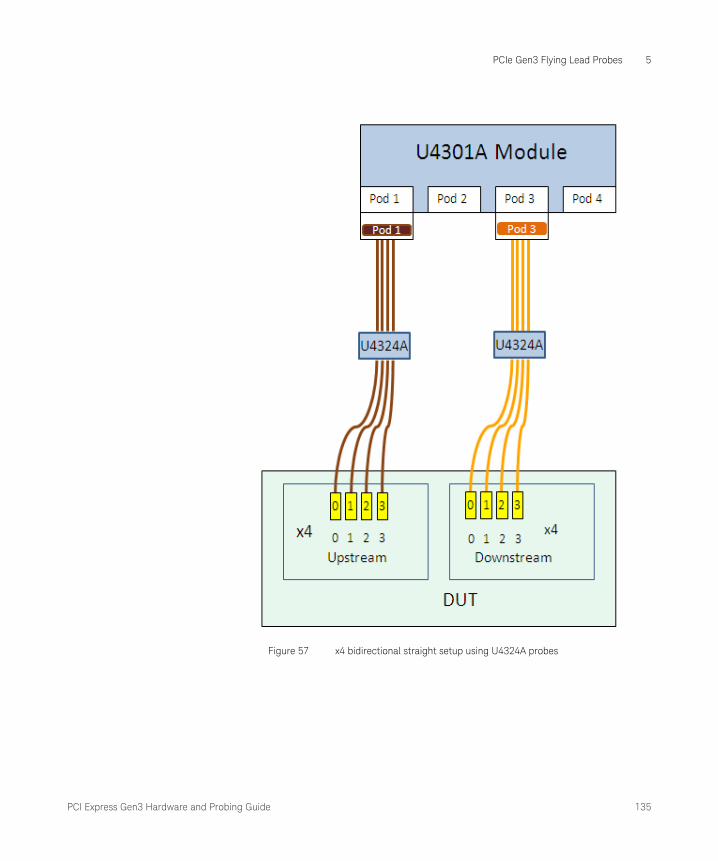
PCI Express Gen3 Hardware and Probing Guide 135
PCIe Gen3 Flying Lead Probes 5
Figure 57 x4 bidirectional straight setup using U4324A probes

136 PCI Express Gen3 Hardware and Probing Guide
5 PCIe Gen3 Flying Lead Probes
x4 bidirectional link swizzled configuration
For a x4 bidirectional swizzled setup, perform the following steps.
1 Plug the module connector of the first U4324A flying lead probe into Pod 1 of the U4301A/B Analyzer module.
2 Plug the module connector of the second U4324A flying lead probe into Pod 3 of the U4301A/B Analyzer module.
3 For the upstream direction, connect the flying lead cables labelled as 0 and 2 of both the probes to the appropriate target points on the DUT via ZIF tips.
4 For the downstream direction, connect the flying lead cables labelled as 1 and 3 of both the probes to the appropriate target points on the DUT via ZIF tips.
The following figures illustrate a x4 bidirectional swizzled setup using U4324A probes.

PCI Express Gen3 Hardware and Probing Guide 137
PCIe Gen3 Flying Lead Probes 5
Figure 58 x4 bidirectional swizzled setup using U4324A probes
For a x8 bidirectional link configuration
You need a single U4301A/B Analyzer module and four U4324A flying lead probes for a x8 bidirectional setup.

138 PCI Express Gen3 Hardware and Probing Guide
5 PCIe Gen3 Flying Lead Probes
Perform the following steps for a x8 bidirectional hardware and probing setup.
1 Plug the module connectors of the four U4324A flying lead probes into Pod 1, 2, 3, and 4 of the U4301A/B Analyzer module.
2 Connect all the flying lead cables of the four probes to the appropriate target points on the DUT via ZIF tips.
The following figure illustrates a x8 bidirectional setup using U4324A probes.
Figure 59 x8 bidirectional setup using U4324A probes

PCI Express Gen3 Hardware and Probing Guide 139
PCIe Gen3 Flying Lead Probes 5
x8 bidirectional link swizzled configuration
For a x8 bidirectional swizzled setup, perform the following steps.
1 Plug the module connectors of the four U4324A flying lead probes into Pod 1, 2, 3, and 4 of the U4301A/B Analyzer module.
2 For the upstream direction, connect the flying lead cables labelled as 0 and 2 of all the four probes to the appropriate target points on the DUT via ZIF tips.
3 For the downstream direction, connect the flying lead cables labelled as 1 and 3 of all the four probes to the appropriate target points on the DUT via ZIF tips.
The following figures illustrate a x8 bidirectional swizzled setup using U4324A probes.

140 PCI Express Gen3 Hardware and Probing Guide
5 PCIe Gen3 Flying Lead Probes
Figure 60 x8 bidirectional swizzled setup using U4324A probes
For two x1 bidirectional links configuration
You need two U4301A/B Analyzer modules and four U4324A flying lead probes for two x1 bidirectional setups.

PCI Express Gen3 Hardware and Probing Guide 141
PCIe Gen3 Flying Lead Probes 5
Perform the following steps for two x1 bidirectional hardware and probing setups.
1 Plug the module connector of the first and second U4324A flying lead probes into Pod 1 and 3 of the U4301A/B Analyzer module 1.
2 Plug the module connectors of the third and fourth U4324A flying lead probes into Pod 1 and 3 of the U4301A/B Analyzer module 2.
3 Connect the flying lead cable labeled as 0 of the four probes to the appropriate target points on the DUT via ZIF tips. Other flying lead cables of the probe will not be connected in this scenario.
The following figure illustrates two x1 bidirectional setups using U4324A probes.

142 PCI Express Gen3 Hardware and Probing Guide
5 PCIe Gen3 Flying Lead Probes
Figure 61 Two x1 bidirectional setups using U4324A probes
For two x2 or x4 bidirectional links configuration
For two x2 or two x4 bidirectional setups, you need the same hardware and probing setup as described above for two x1 bidirectional setups. The only difference would be that you need to connect:
• the flying lead cables labeled as 0 and 1 of the four probes to the appropriate target points on the DUT via ZIF tips for a x2 setup.

PCI Express Gen3 Hardware and Probing Guide 143
PCIe Gen3 Flying Lead Probes 5
• all the four flying lead cables of the four probes to the appropriate target points on the DUT via ZIF tips for a x4 setup.
The following figures illustrate two x2 and two x4 bidirectional setups using U4324A probes.
Figure 62 Two x2 bidirectional setups using U4324A probes

144 PCI Express Gen3 Hardware and Probing Guide
5 PCIe Gen3 Flying Lead Probes
Figure 63 Two x4 bidirectional setups using U4324A probes
PCI Express Gen3 Hardware and Probing Guide 145
PCIe Gen3 Flying Lead Probes 5
Setting up a x16 upstream and downstream configuration using U4324A probes
If you want to probe and capture upstream as well downstream data with x16 link width, you need two U4301A/B Analyzer modules and eight U4324A probes
Perform the following steps for a x16 upstream and downstream hardware and probing setup.
1 Plug the module connectors of the four U4324A flying lead probes into Pod 1, 2, 3, and 4 of the U4301A/B Analyzer module that you are using as the upstream module.
2 Plug the module connectors of the remaining four U4324A flying lead probes into Pod 1, 2, 3, and 4 of the U4301A/B Analyzer module that you are using as the downstream module.
3 Connect all the four flying lead cables of all the eight probes to the appropriate target points on the DUT via ZIF tips.
The following figure illustrates a x16 upstream and downstream setup.

146 PCI Express Gen3 Hardware and Probing Guide
5 PCIe Gen3 Flying Lead Probes
Figure 64 x16 upstream and downstream setup using U4324A probes

PCI Express Gen3 Hardware and Probing Guide
6 U4328A M.2 (M-key) Interposer
U4328A M.2 (M-key) Interposer Description / 148 M.2 Connector Pinout / 151 Scope Probe Connections on the U4328A Interposer / 154 Assembling the U4328A Interposer / 155 Setting up a Bidirectional (x1 to x4) Configuration using the U4328A Interposer / 157
This chapter provides information on how to set up, configure, and use the U4328A M.2 (M-key) Interposer with a U4301 Analyzer module.

148 PCI Express Gen3 Hardware and Probing Guide
6 U4328A M.2 (M-key) Interposer
U4328A M.2 (M-key) Interposer Description
The U4328A M.2 (M-key) Interposer interfaces between a PCIe Solid State Drive (SSD) and the M.2 connector on a host system (SUT).
This interposer is compatible with Keysight/Agilent U4301B and U4301A PCIe Protocol Analyzer modules and allows you to probe x1 to x4 PCIe lanes provided as per the M.2 specifications.
The following figure displays the cable assembly of the U4328A interposer.
Figure 65 U4328A interposer cable assembly
Reference Clock Connector
The U4328A interposer provides reference clock connections for situations where it is necessary to probe the reference clock from the DUT.
You can probe the REFCLKP and REFCLKN signals using the Reference Clock Connector available on the interposer cable labeled “Even”.
Refer to the M.2 Connector pinout diagram on page 151 to view the pins associated to REFCLKP and REFCLKN signals.
Even and Odd Module Connectors(To connect to U4301 Module)
Cable Connector(Connects to M.2 type M Connector on SUT)
Interposer Connector(Connects to DUT)

PCI Express Gen3 Hardware and Probing Guide 149
U4328A M.2 (M-key) Interposer 6
Figure 66 Reference clock Connector
U4328A Interposer Dimensions
The tip-to-tip dimension of the Interposer cable is given below in Millimeters.
Figure 67 Interposer cable dimension (in Millimeters)

150 PCI Express Gen3 Hardware and Probing Guide
6 U4328A M.2 (M-key) Interposer
Interposer Characteristics
Characteristic Value
PCIe lane probe resistance 250 Ohms per side
REFCLK probe resistance 1K Ohms per side
Scope probe connections CLKREQ#, PERST#, PEWAKE#, +/- Current senseRefer to page 154 for pinout details.
Current sense resistor (for use with N2820A)
50 mOhms, 3A Max
Adapter Height 12.8 mm
Supplied adapters 22x30, 22x42, 22x60, 22x80, and 22x110

PCI Express Gen3 Hardware and Probing Guide 151
U4328A M.2 (M-key) Interposer 6
M.2 Connector Pinout
The following figure illustrates the 75 positions (with 67 pins) connector of the U4328A interposer followed by the pinout for this M.2 connector.
Figure 68 M.2 Connector Pins Assignment
In the M.2 connector pinout below:
• Signals highlighted with red are targeted to the U4328A cable labeled Even.
• Signals highlighted with brown are targeted to the U4328A cable labeled Odd.
• NC indicates Not Connected.
Signal Name Pin # Pin # Signal Name
GND 75
GND 73 74 V+3.3
GND 71 72 V+3.3
PEDET 69 70 V+3.3
NC 67 68 SUSCLK
KEY 65 66 KEY
KEY 63 64 KEY
KEY 61 62 KEY
KEY 59 60 KEY
GND 57 58 NC
REFCLKP 55 56 NC
REFCLKN 53 54 PEWAKE#
GND 51 52 CLKREQ#

152 PCI Express Gen3 Hardware and Probing Guide
6 U4328A M.2 (M-key) Interposer
Mapping of U4301 Analyzer Channels with Probed Signals
The following table maps the signals probed using the Odd and Even cables of the U4328A interposer with the channels on Pod 1 and Pod 2 of a U4301 Analyzer module. The channels on Pod 1 are used to probe the lanes 0-3 in the Downstream direction and the channels on Pod 2 are used to probe the lanes 0-3 in the Upstream direction.
Down0p 49 50 PERST#
Down0n 47 48 NC
GND 45 46 NC
Up0p 43 44 NC
Up0n 41 42 NC
GND 39 40 NC
Down1p 37 38 DEVSLP
Down1n 35 36 NC
GND 33 34 NC
Up1p 31 32 NC
Up1n 29 30 NC
GND 27 28 NC
Down2p 25 26 NC
Down2n 23 24 NC
GND 21 22 NC
Up2p 19 20 NC
Up2n 17 18 V+3.3
GND 15 16 V+3.3
Down3p 13 14 V+3.3
Down3n 11 12 V+3.3
GND 9 10 LED1#
Up3p 7 8 NC
Up3n 5 6 NC
GND 3 4 V+3.3
GND 1 2 V+3.3
Signal Name Pin # Pin # Signal Name

PCI Express Gen3 Hardware and Probing Guide 153
U4328A M.2 (M-key) Interposer 6
U4301 Pod Channels Signal Name
Pod 1 (Odd cable of U4328A connects to this Pod)
Channel 0 Down0pDown0n
Channel 1 Down1pDown1n
Channel 2 Down2pDown2n
Channel 3 Down3pDown3n
Pod 2(Even cable of U4328A connects to this Pod)
Channel 0 Up0pUp0n
Channel 1 Up1pUp1n
Channel 2 Up2pUp2n
Channel 3 Up3pUp3n
Reference Clock REFCLKPREFCLKN

154 PCI Express Gen3 Hardware and Probing Guide
6 U4328A M.2 (M-key) Interposer
Scope Probe Connections on the U4328A Interposer
The following screen displays the pinout for the scope probe connections available on the U4328A interposer.
Pinout for Scope Probe Connections
Current Sense - Current Sense +
GND GND
GND PDWAKE#
PERST# CLKREQ#

PCI Express Gen3 Hardware and Probing Guide 155
U4328A M.2 (M-key) Interposer 6
Assembling the U4328A Interposer
U4328A Interposer Shipping Kit
The interposer shipping kit contains the cable assembly along with the following parts that you need to complete the interposer assembly.
Part Description Quantity
M2 x 0.4 x 4L Flat Head Screw 4
M3 x 0.5 x 2.5L Wafer Head Screw 4
M3 Hex Standoff Male/Female 1
4.5 Hex Driver 1
Screw Driver, Phillips #1 1
Mounting Bases 1 each for the displayed dimensions to support all standard M.2 sizes.
Above-mentioned parts are replaceable. You can order these as Replacement Parts Kit - U4328-68702.
NOTEThe interposer shipment includes a Quick Start guide (part number - U4328-92000) that provides a step-by-step procedure for connecting the interposer to the DUT and SUT using the parts supplied in the shipment.
You can also download this guide from the Document Library tab at
http://www.keysight.com/find/U4328A.

156 PCI Express Gen3 Hardware and Probing Guide
6 U4328A M.2 (M-key) Interposer
The following figure displays the U4328A interposer assembled and connected to DUT and SUT as per the steps outlined in its Quick Start Guide.
Figure 69 U4328A interposer connected to DUT and system board
CAUTIONFRAGILE! EXERCISE CARE WHILE BENDING AND FLEXING THE INTERPOSER ASSEMBLY.
DUT)
System Board

PCI Express Gen3 Hardware and Probing Guide 157
U4328A M.2 (M-key) Interposer 6
Setting up a Bidirectional (x1 to x4) Configuration using the U4328A Interposer
You can probe a x1, x2, or x4 bidirectional PCIe link configuration using a U4328A interposer attached to a single U4301 Analyzer module.
After the interposer assembly is complete, perform the following steps to complete the hardware setup for a bidirectional link configuration using U4328A.
1 Connect the interposer’s module connector labeled Odd to Pod 1 of the U4301 Analyzer module. This will probe the lanes 0-3 in the Downstream direction.
2 Connect the interposer’s module connector labeled Even to Pod 2 of the U4301 Analyzer module. This will probe the lanes 0-3 in the Upstream direction.
The following figure illustrates a bidirectional setup using the U4328A interposer.

158 PCI Express Gen3 Hardware and Probing Guide
6 U4328A M.2 (M-key) Interposer
After the hardware setup for probing is complete, configure the link setup in the Logic and Protocol Analyzer GUI as per the steps described in the Specifying the Connection Setup topic in the U4301 PCIe Gen3 Analyzer Online Help. This Online help is available with the Logic and Protocol Analyzer GUI.

PCI Express Gen3 Hardware and Probing Guide
7 U4330A U.2 (SFF-8639) Interpos-er for PCIe Gen3
U4330A U.2 Interposer Description / 160 Connecting the U4330A U.2 Interposer to a PCIe SSD Drive and SUT / 164 U.2 Connector Pinout (as seen in the Receptacle View) / 165 Scope Probe Connections on the U4330A U.2 Interposer / 167 U4330A Link Configuration Scenarios / 168
This chapter provides information on how to set up, configure, and use the U4330A U.2 (SFF-8639) Interposer for PCIe Gen3 with a U4301 Analyzer module.
NOTEThe SSD Form Factor Working Group (SFFWG) announced that the PCIe 3.0 x4 SFF-8639 connector will now be referred to as the U.2 connector. When referencing to the probing connection, U.2 will be used throughout this chapter on the U4330A U.2 interposer.

160 PCI Express Gen3 Hardware and Probing Guide
7 U4330A SFF-8639 Interposer
U4330A U.2 Interposer Description
The U4330A U.2 Interposer probes PCIe traffic between a PCIe Solid State Drive (SSD) and a PCIe host system (SUT).
This interposer is compatible with Keysight/Agilent U4301B and U4301A PCIe Protocol Analyzer modules and allows you to probe x1 to x4 Upstream and Downstream PCIe lanes as per the U.2 SFF-8639 interconnection standard.
A single U4330A U.2 interposer can support the following link configurations and requires the following number of U4301A/B modules for these configurations.
Single Port Configuration(single x1, x2, or x4 bid irectional l ink)
Dual Port Configuration(dual -two independent x1 or x2
bid irectional l inks)
U4330A U.2 interposer needed 1 1
U4301A/B module(s) needed 1 2*
*NOTE: A U4301A/B module can analyze a single bidirectional link at a time. To simultaneously analyze two independent links, you need two U4301 modules.

PCI Express Gen3 Hardware and Probing Guide 161
U4330A SFF-8639 Interposer 7
The following figure displays a U4330A U.2 interposer.
Figure 70 U4330A U.2 interposer
Reference Clock Connectors
The U4330A U.2 interposer provides reference clock connections for situations where it is necessary to probe the reference clock from the DUT.
You can probe the RefClkP and RefClkN signals using the Reference Clock Connectors (see Figure 70) available on the interposer cables labeled “Even” and “Odd”.
In a single port configuration scenario, RefClk0 available on the Odd cable of the interposer may be used. In a dual-port configuration scenario, RefClk0 available on the Odd cable is used for the primary port, Port A and RefClk1 available on the Even cable is used for the dual port, Port B.
Refer to the U.2 Connector pinout table on page 165 to view the pins associated to RefClkP and RefClkN signals.
Even and Odd Module Connectors(To connect to U4301 Module)
U.2 Connector(Connects to U.2 Connector of the d isk drive)
Reference Clock Connectors
For RefClk1 For RefClk0

162 PCI Express Gen3 Hardware and Probing Guide
7 U4330A SFF-8639 Interposer
U4330A U.2 Interposer Dimensions
The dimensions of the interposer are given below.
Figure 71 Side View of the interposer when connected to a hard disk drive
Figure 72 Left end view View of the interposer when connected to a hard disk drive
Hard Disk Drive
952.6 mm[37.5 inches]
13.3 mm[.5 inches]
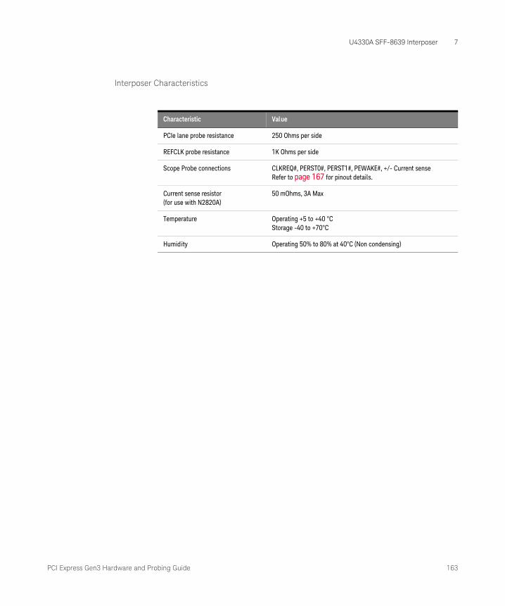
PCI Express Gen3 Hardware and Probing Guide 163
U4330A SFF-8639 Interposer 7
Interposer Characteristics
Characteristic Value
PCIe lane probe resistance 250 Ohms per side
REFCLK probe resistance 1K Ohms per side
Scope Probe connections CLKREQ#, PERST0#, PERST1#, PEWAKE#, +/- Current senseRefer to page 167 for pinout details.
Current sense resistor (for use with N2820A)
50 mOhms, 3A Max
Temperature Operating +5 to +40 °CStorage -40 to +70°C
Humidity Operating 50% to 80% at 40°C (Non condensing)

164 PCI Express Gen3 Hardware and Probing Guide
7 U4330A SFF-8639 Interposer
Connecting the U4330A U.2 Interposer to a PCIe SSD Drive and SUT
The following figure displays the U4330A U.2 interposer connected to the SSD drive and SUT as per the steps outlined in its Quick Start Guide.
Figure 73 U4330A U.2 interposer connected to a disk drive
NOTEThe interposer shipment includes a Quick Start guide (part number - U4330-92000) that provides a step-by-step procedure for connecting the interposer to the SSD drive and SUT. You can also download this guide from the Document Library tab at:
http://www.keysight.com/find/U4330A.
Disk Drive
CAUTIONFRAGILE! EXERCISE CARE WHILE BENDING AND FLEXING THE INTERPOSER.

PCI Express Gen3 Hardware and Probing Guide 165
U4330A SFF-8639 Interposer 7
U.2 Connector Pinout (as seen in the Receptacle View)
The following table provides the mapping between the pins and signals for the 68-positions U.2 connector of the U4330A interposer.
In the U4330A U.2 connector pinout below:
• Signals highlighted with brown are targeted to the U4330A cable labeled Odd.
• Signals highlighted with red are targeted to the U4330A cable labeled Even.
Signal Name Pin # Pin # Signal Name
E7 REFCLKp0
GND S1 E8 REFCLKn0
S0Tp S2 E9 GND
S0Tn S3 E10 PETp0
GND S4 E11 PETn0
S0Rn S5 E12 GND
S0Rp S6 E13 PERn0
GND S7 E14 PERp0
E15 GND
E16 RSVD_E16
REFCLKp1 E1 S8 GND
REFCLKn1 E2 S9 S1Tp
3P3VAUX E3 S10 S1Tn
PERST1# E4 S11 GND
PERST0# E5 S12 S1Rn
RSVD_E6 E6 S13 S1Rp
S14 GND
S15 RSVD_S15
WAKE# P1 S16 GND
SPCIERST P2 S17 PETp1
CLKREQ# P3 S18 PETn1
IFDET# P4 S19 GND

166 PCI Express Gen3 Hardware and Probing Guide
7 U4330A SFF-8639 Interposer
GND P5 S20 PERn1
GND P6 S21 PERp1
5V_P7 P7 S22 GND
5V_P8 P8 S23 PETp2
5V_P9 P9 S24 PETn2
PRSNT# P10 S25 GND
ACTIVITY P11 S26 PERn2
GND P12 S27 PERp2
12V P13 S28 GND
12V P14 E17 PETp3
12V P15 E18 PETn3
E19 GND
E20 PERn3
E21 PERp3
E22 GND
E23 SMCLK
E24 SMDAT
E25 DUALPORTEN#
Signal Name Pin # Pin # Signal Name

PCI Express Gen3 Hardware and Probing Guide 167
U4330A SFF-8639 Interposer 7
Scope Probe Connections on the U4330A U.2 Interposer
The following screen displays the pinout for the scope probe connections available on the U4330A interposer.
Pinout for Scope Probe Connections
Current Sense - Current Sense +
GND GND
PERST0# WAKE#
PERST1# CLKREQ#
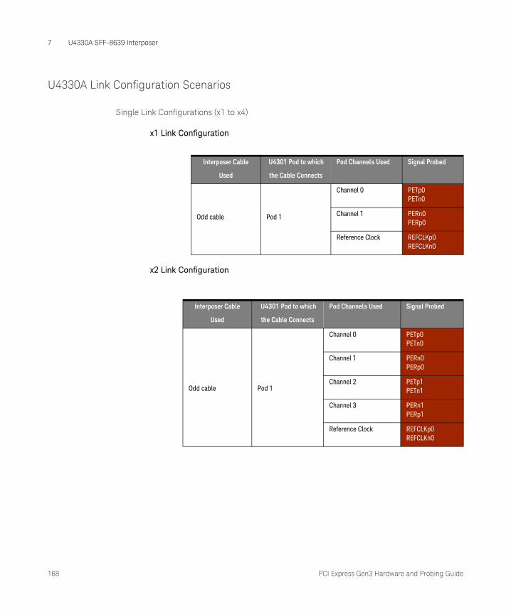
168 PCI Express Gen3 Hardware and Probing Guide
7 U4330A SFF-8639 Interposer
U4330A Link Configuration Scenarios
Single Link Configurations (x1 to x4)
x1 Link Configuration
x2 Link Configuration
Interposer Cable
Used
U4301 Pod to which
the Cable Connects
Pod Channels Used Signal Probed
Odd cable Pod 1
Channel 0 PETp0PETn0
Channel 1 PERn0PERp0
Reference Clock REFCLKp0REFCLKn0
Interposer Cable
Used
U4301 Pod to which
the Cable Connects
Pod Channels Used Signal Probed
Odd cable Pod 1
Channel 0 PETp0PETn0
Channel 1 PERn0PERp0
Channel 2 PETp1PETn1
Channel 3 PERn1PERp1
Reference Clock REFCLKp0REFCLKn0

PCI Express Gen3 Hardware and Probing Guide 169
U4330A SFF-8639 Interposer 7
x4 Link Configuration
Dual Link (Port A and B) x1 or x2 Configurations
Interposer Cable
Used
U4301 Pod to which
the Cable Connects
Pod Channels Used Signal Probed
Odd cable Pod 1
Channel 0 PETp0PETn0
Channel 1 PERn0PERp0
Channel 2 PETp1PETn1
Channel 3 PERn1PERp1
Reference Clock REFCLKp0REFCLKn0
Even cable Pod 2
Channel 0 PETp2PETn2
Channel 1 PERn2PERp2
Channel 2 PETp3PETn3
Channel 3 PERn3PERp3
NOTEIn a dual link configuration:
- the Odd cable of the U4330A interposer is used for the primary port, Port A.
- the Even cable of the U4330A interposer is used for the dual port, Port B.

170 PCI Express Gen3 Hardware and Probing Guide
7 U4330A SFF-8639 Interposer
Analyzing One Link at a Time
Analyzing Both Links Simultaneously
In this specific scenario, you need two U4301 Analyzer modules to analyze two links simultaneously.
Interposer Cable
Used
U4301 Pod to which
the Cable Connects
Pod Channels Used Signal Probed
For Port A (Link 1)
Odd cable Pod 1 Channel 0 PETp0PETn0
Channel 1 PERn0PERp0
Channel 2 PETp1PETn1
Channel 3 PERn1PERp1
Reference Clock REFCLKp0REFCLKn0
For Port B (Link 2)
Even cable Pod 1 Channel 0 PETp2PETn2
Channel 1 PERn2PERp2
Channel 2 PETp3PETn3
Channel 3 PERn3PERp3
Reference Clock REFCLKp1REFCLKn1

PCI Express Gen3 Hardware and Probing Guide 171
U4330A SFF-8639 Interposer 7
After the hardware setup for probing is complete, configure the link setup in the Logic and Protocol Analyzer GUI as per the steps described in the Specifying the Connection Setup topic in the U4301 PCIe Gen3 Analyzer Online Help. This Online help is available with the Logic and Protocol Analyzer GUI.
Interposer Cable
Used
U4301 Module Used U4301 Pod to which
the Cable Connects
Pod Channels Used Signal Probed
For Port A (Link 1)
Odd cable U4301 module <1> Pod 1 Channel 0 PETp0PETn0
Channel 1 PERn0PERp0
Channel 2 PETp1PETn1
Channel 3 PERn1PERp1
Reference Clock REFCLKp0REFCLKn0
For Port B (Link 2)
Even cable U4301 module <2> Pod 1 Channel 0 PETp2PETn2
Channel 1 PERn2PERp2
Channel 2 PETp3PETn3
Channel 3 PERn3PERp3
Reference Clock REFCLKp1REFCLKn1

172 PCI Express Gen3 Hardware and Probing Guide
7 U4330A SFF-8639 Interposer

PCI Express Gen3 Hardware and Probing Guide 173
PCI Express Gen3 Hardware and Probing Guide 173
Index
Aadd-in card connector, 35
Ccables, 36connecting midbus probe, 93
Eedge connector, 21, 35electrical design for reference clock
connector, 63endpoint, U4305A exerciser card
as, 26
Ffeature list for midbus probe, 51flying lead cable, 102flying lead probe, 100footprint dimensions and
specifications, midbus 3.0, 54footprint for reference clock
connector, 58footprint, midbus 3.0, 54
Hheat protection cover, 39heat sink, 39
Iinstallation instructions, Soft Touch
midbus probes, 93Interface Port, 30
Kkeep-out volume, midbus 3.0
probe, 57keep-out volume, U4305A/U4305B
exerciser card, 28
LLane status LEDs, 31link configuration support, 52load model, midbus 3.0 probes, 62load model, reference clock
connector, 63
MM.2 connector pinout, 148mechanical strain relief, 107midbus 3.0 probe
characteristics, 97, 104midbus 3.0 probes, 51, 99midbus 3.0 probes, load model, 62
NN5426A ZIF Tip Dimensions, 104N5426A ZIF tip kit, 102
PPCIe Gen3 Flying Lead probes, 99pin assignments, 64Pods 1-4, 30ports, 36power supply connector (front
bracket), 39power supply connector (on front
bracket), 22
Rreference clock connector load
model, 63reference clock connector,
keep-out volume, 58reset button, 39retention module dimensions, 57retention modules, 52root complex, U4305A exerciser
card as, 27routing considerations, midbus 3.0
footprint, 60
Ssafety summary, 3Soft Touch midbus 3.0 probes, 51speed LEDs, 31status LED (on front bracket), 22status LED1, 39status LED2, 39status LEDs (on board), 22
TTRIG IN connector, 22TRIG OUT connector, 22Trigger In/Out, 32
UU.2, 160U.2 connector pinout, 161U4305A exerciser card
components, 20U4305A exerciser card features, 19U4305A exerciser card status
LEDs, 23U4305A_Fig_As_Endpoint, 26

174 PCI Express Gen3 Hardware and Probing Guide
Index
U4305A_Fig_As_Root_Complex, 27
U4305A/U4305B exerciser card, 18U4321A Solid Slot Interposer
Card, 33U4322A midbus probe, 51U4324 pod and channel
labels, 110U4324 Reference Clock
Connector, 102U4324A, 100U4328A, 148U4328A parts, 155U4328A scope probe
connections, 154U4330A, 160U4330A scope probe
connections, 167USB connector, 22
Xx16 Straight Footprint, 64
Zzero insertion force connector, 102ZIF tip, 102

PCI Express Gen3 Hardware and Probing Guide 175

This information is subject to change without notice.© Keysight Technologies 2015Edition 6 October 2015
*U4301-97000*www.keysight.com