pci target interface discussion: using pci-104 pci interface development solution review june 15,...
TRANSCRIPT

PCI Target InterfaceDiscussion: Using PCI-104
PCI Interface Development Solution Review
June 15, 2006

15-JUN-06 QUINTRON SYSTEMS 2
PCI Local Bus Key Definitions PCI specification classifies two different AGENTS
used in every PCI burst transfer: Initiator (Bus Master) Target (Addressed by the Initiator)
Single Versus Multi-Function PCI Devices Each Function has its own Configuration Space Each Function Can Generate a Unique Interrupt
Signal Naming Conventions “Low-Active” signal names are indicated with the use of the
“#” symbol.

15-JUN-06 QUINTRON SYSTEMS 3
PCI Bus Details
PCI Bus is unterminated - relies on Reflective Wave Switching Signal must be valid on the first reflected wave Detailed Electrical Spec to guarantee proper signal switching

15-JUN-06 QUINTRON SYSTEMS 4
Configuration Space (Rev 2.2) Each Function has a Configuration
space is a 256-byte area inside each PCI device that contains information about the device.
At power-up, the system scans the configuration space of all devices on the PCI bus and then assigns each device a unique base address and an interrupt level.
The first 64 bytes (00h – 3Fh) make up the standard configuration header, predefined by the PCI spec, see adjacent figure.
The remaining 192 bytes (40h – FFh) represent user-definable configuration space
This region may store, for example, information specific to a PC card for use by its accompanying software driver

15-JUN-06 QUINTRON SYSTEMS 5
Base Address Register (Memory) Base address Registers (BAR) allow an agent to be
mapped dynamically into Memory Space
BAR BIT MAPMEMORY EXAMPLE
04h
32-BIT BASE ADDRESS (BLOCK SIZE & AND ADDRESS RANGE)READ/WRITE
0 0 0 0
I/O MEMORY SPACE INDICATOR (0 = MEMORY)
DECODER TYPE
PREFETCHABLE (0 = NO)
BASE ADDRESS (32-BIT)
D31 D00D01D02D03
TYPE (00 = 32-Bit: LOCATE IN LOWER 4GBYTE)
D04
MEMORY BASE ADDRESS REGISTER4,294,967,296 Memory Locations
Maximum (32-Bit - 4 GBYTE) SMALLESTMEMORYDECODER = 16ADDRESSES
TYPE 01 = RESERVED IN REVISION 2.2
TYPE 11 = RESERVED
TYPE 10 = 64-BIT

15-JUN-06 QUINTRON SYSTEMS 6
Base Address Register (I/O) Base address Registers (BAR) allow an agent to be
mapped dynamically into I/O Space Not Recommended for New Designs.
BAR BIT MAPI/O EXAMPLE
05h
32-BIT BASE ADDRESS (BLOCK SIZE & AND ADDRESS RANGE)READ/WRITE
0READ
1READ
I/O MEMORY SPACE INDICATOR (1 = I/O)
RESERVED (MUST = 0)
(256 MAX LOCATIONS)
D31 D00D01D02
SMALLESTMEMORYDECODER = 4ADDRESSES
I/O BASE ADDRESS REGISTER256 Memory Locations MAXIMUM
PER I/O BAR

15-JUN-06 QUINTRON SYSTEMS 7
Example Memory BAR

15-JUN-06 QUINTRON SYSTEMS 8
Command Bus C/BE#[3:0]

15-JUN-06 QUINTRON SYSTEMS 9
Byte Lanes: Local Byte Enables C/BE#[3:0] 32-Bit Burst Transfer
8 X 256MEMORY
LD[7:0]
LA7
LA6
LA5
LA4
LA3
LA2
A7
A6
A5
A4
A3
A2
A1
A0
8 X 256MEMORY
LD[15:8]
LA7
LA6
LA5
LA4
LA3
LA2
A7
A6
A5
A4
A3
A2
A1
A0
EN#
EN#
LBE1#
CS#
LBE0#
LA8
LA8
LA9
LA9
8 X 256MEMORY
LD[23:16]
LA7
LA6
LA5
LA4
LA3
LA2
A7
A6
A5
A4
A3
A2
A1
A0
8 X 256MEMORY
LD[31:24]
LA7
LA6
LA5
LA4
LA3
LA2
A7
A6
A5
A4
A3
A2
A1
A0
EN#
EN#
LBE3#
CS#
LBE2#
LA8
LA8
LA9
LA9
32-BIT X 256 DATA DECODINGLBE[3:0]# Encoding 1024 BYTES
0x0000x0040x0080x00C0x010

15-JUN-06 QUINTRON SYSTEMS 10
PCI Write Example (Burst of 4)

15-JUN-06 QUINTRON SYSTEMS 11
PC/104-Plus VS PCI-104
The PC/104-PLUS contains both: PC-104 ISA Bus A third connector opposite the ISA connectors
supports the PCI bus (PCI-104 Form Factor). PCI-104 Interface (Proposed for Target)
No ISA Bus Interface Strictly a 32-Bit PCI Interface

15-JUN-06 QUINTRON SYSTEMS 12
PCI-104 Board Stacking
Design uses PCI-104 Non-Stackthrough Module (as shown to the right)
No Support for ISA Interface (If PC/104-Pus SBC is used)

15-JUN-06 QUINTRON SYSTEMS 13
PCI-104 Versus PCI Local Bus The PCI-104 bus connector is a
4x30 (120-pin) 2mm pitch stack-through connector as opposed to the 124-pin edge connector on standard 32-bit PCI.
The 120-pin PCI-104 form factor does not support 64-bit Extensions, JTAG, PRSNT (Card Present), or CLKRUN signals.

15-JUN-06 QUINTRON SYSTEMS 14
PCI-104 Standards
Based on PCI-104 Specification Version 1.0 (November 2003)
PCI-104 Based on Revision 2.2 of PCI Local Bus Architecture Specification. Maximum CLK (supported) = 33MHz Maximum Data Bus Width = 32-bit
Maximum Theoretical (Bursting) Data Transfer Rate = 132Mbytes Second
Bits 8
)10 X (33 X 32Bits(Transfer) 132
6
Mbyte

15-JUN-06 QUINTRON SYSTEMS 15
PCI Pin List
The PCI bus has been simulated at 33MHz. For the purpose of this specification, 66MHz is not supported. To support future enhancements, the M66EN signal should be grounded on any module that cannot support 66MHz and left open for modules that can support a 66MHz clock.

15-JUN-06 QUINTRON SYSTEMS 16
PCI-104 120-Pin Bus Assignments IDSEL, CLK, INTx# are
Distributed using separate Pins on connector.
Host Boards implementing“5 volt PCI signaling” are not required to supply 3.3 volts to the modules, but must provide a bus and decoupling. Host Boards implementing “3.3 volt PCI signaling” are not required to supply 5 volts to the modules, but must provide a bus and decoupling.
Trace Lengths Varies, depending on Agent’s position in the stack.

15-JUN-06 QUINTRON SYSTEMS 17
SOW Interface Requirements
QUINTRON has provided the following requirements: Support 5.0/3.3V Signaling Explore IP CORE for FPGA versus dedicated
Interface IC Support 32, 16, and 8-Bit bus widths facilitating
linear addressing. TQFP Package (Avoid BGA – Not a Requirement) Research DMA & Bursting support.

15-JUN-06 QUINTRON SYSTEMS 18
Prototype Design Steps
Research and propose Technology solution for Interface Design Design a Prototype to model a KEYSET based on
PCI Target, meeting the following requirements: Memory-mapped access (8/16/32-bit) to devices, including:
T1 Framer(s) (DS2155) 16 bit x 2K Dual-Port RAM 8/16-bit Read/Write registers 8-bit x 512 byte FIFO Breadboard space/expansion connector for add-on circuitry

15-JUN-06 QUINTRON SYSTEMS 19
Evaluation PCI-104 Block Diagram
Address Decoder& Additional 32-Bit Test
Registers.
DA
TA
[31:24]D
AT
A[23:16]
DA
TA
[15:8]D
AT
A[7:0]
DA
TA
[31:24]D
AT
A[23:16]
DA
TA
[15:8]D
AT
A[7:0]
DP-R/W(L+R)
FIFO_RD/WT(R)#
FIFO-EN(R)#
2K X
16-Bit
DU
AL
PO
RT
RA
M(N
O P
IPE
LIN
E)
PCI-104120-PINCONN
NO STACK-THROUGH
PCITARGETInterface
AD[31:0]
C/BE#[3:0]
PAR
FRAME#
TRDY#
IRDY#
STOP#
DEVSEL#
IDSEL0
CLK0 (33MHz)
RST#
PERR#
SERR#
INTA#
INTB#
INTC#
INTD#
+12
-12
+5
+3.3
GND
VI/O (+5/+3.3)
Note 1: Host Boards implementing “5 volt PCI signaling” are not required to supply 3.3 volts to the modules,but must provide a bus and decoupling. Host Boards implementing “3.3 volt PCI signaling” are notrequired to supply 5 volts to the modules, but must provide a bus and decoupling.
PCI/104-PLUSCOMPATIBLE
HOST
ADD[31:0]
DATA[31:00]
DS
2155T1CTL_PTx
DP-BL0#DP-BL1#
DP-EN(L+R)#
LIU
8 X 512FIFO
FIFO-EN(L)#FIFO_RD/WT(L)#
BUSY (TRDY# WAIT-STATE)
BYTE-LANE 3#
BYTE-LANE 2#
BYTE-LANE 1#
BYTE LANE 0#
BR
EA
DB
OA
RD
HE
AD
ER
S(O
OH
M R
ES
IST
OR
S)
TE
ST
CO
NN
EC
TO
RS
GP-I/O
DATA[7:0]
DATA[31:0]
DATA[15:0]
DATA[7:0]
ADD[7:0]
ADD[12:1]
ADD[31:1]
PCI-104 Evaluation BoardSINGLE TARGET APPLICATION
Block Diagram
POINT-TO-POINTCONNECTION DESIGNON FOLLOWING SIGNALS:
1) CLK02) IDSEL03) INTA# - INTD#
LA TEST
LA TEST
LA TEST
LA TEST
LA TEST 25-FEB-06
CLK1CLK2CLK3
IDSEL1IDSEL2IDSEL3
ADD[12:1]
DATA[15:0]

15-JUN-06 QUINTRON SYSTEMS 20
Interface Design Technology
Two Methods to develop Interface IP Core (Targeted FPGA must support 5.0V and
3.3V signaling), limited options. Use dedicated PCI Target Device, such as
PLX9030 (verify life expectancy).

15-JUN-06 QUINTRON SYSTEMS 21
Intellectual Property Evaluation
IP Core manufactures were evaluated based on the following guidelines: Support Older FPGA architectures to meet 5V
interface requirement. Support TQFP FPGA (Non BGA Packages) Vendor’s Engineering Support Vendor Pricing for IP Core and Support

15-JUN-06 QUINTRON SYSTEMS 22
IP Core Manufactures Evaluated
The Following is a List of Intellectual Property Core companies Evaluated: ALTERA (Free Core) Eureka PLDA

15-JUN-06 QUINTRON SYSTEMS 23
Review of ALTERA’s IP Core (Rejected)
Currently IP core revision does not support older FPGA families, no 5V support (see adjacent table of Device Family Support
Supports Low-Cost MAX II Family (No 5V).

15-JUN-06 QUINTRON SYSTEMS 24
Review of EUREKA Technologies EC125 PCI Target (Rejected) The default ALTERA family chosen by the IP Core was STRATIX
(no 5V Support). DMA Support optional (Cost not researched see below).
Retarget design to ACEX family, and the compiler fitted design into EP1K50FC256-1, which is a BGA package (family evaluation only, compile instantiate IP Core for evaluation only): Timing parameters not met in ACEX Family Poor Tech Support IP Core Price: $4,950 Maintenance
service for the first year is 18% of the licensefee ($891.00)

15-JUN-06 QUINTRON SYSTEMS 25
PLDA IP PCI-Target Core Evaluation PLDA is headquartered in
France with a Sales Office in San Jose.
Package included a Project setup wizard

15-JUN-06 QUINTRON SYSTEMS 26
PLDA Wizard

15-JUN-06 QUINTRON SYSTEMS 27
Sample Design Using PLDA Core
VCCCLK INPUT
VCCIDSEL INPUT
VCCLOCK INPUT
VCCFRAME INPUT
VCCC-BE/[3..0] INPUT
VCCIRDY/ INPUT
VCCS_RES[2..0] INPUT
VCCS_INTREQ[1..0] INPUT
VCCRESET/ INPUT
VCCm66en INPUT
INTA/OUTPUT
TRDY/OUTPUT
STOP/OUTPUT
DEVSEL/OUTPUT
PERR/OUTPUT
SERR/OUTPUT
INTB/OUTPUT
S_ADDR[20..0]OUTPUT
S_READOUTPUT
S_WRITEOUTPUT
BYTE_LANES[3..0]OUTPUT
TESTOUTPUT
VCCPARBIDIR
VCCAD[31..0]BIDIR
VCCS_DATA[31..0]BIDIR
clk_pci
rst_pci
idsel_pci
lock_pci
m66en_pci
f rame_pci
cbe_pci[3..0]
irdy _pci
s_response[2..0]
s_data_in[31..0]
s_intrequest[1..0]
prot1_in[1..0]
s_sm[7..0]
s_busmode[2..0]
s_f unction
s_addr[63..0]
s_bar[7..0]
s_read
s_write
s_64f lag
s_data_out[31..0]
s_by tev alid[3..0]
s_by tecount[12..0]
pm_resetn[1..0]
prot0_out
prot1_out
ad_pci[31..0]
trdy _pci
stop_pci
dev sel_pci
par_pci
perr_pci
serr_pci
inta_pci
intb_pci
PCI104
inst
02
CONSTANT0
inst1
DFFdata[7..0]
clock
enableq[7..0]
TestReg8
inst2
DFFdata[7..0]
clock
enableq[7..0]
TestReg8
inst3
DFFdata[7..0]
clock
enableq[7..0]
TestReg8
inst4
DFFdata[7..0]
clock
enableq[7..0]
TestReg8
inst5
compare
datab[]=1048576
dataa[63..0]aeb
AddressCompare
inst6
AND3
inst7
AND3
inst8
AND3
inst9
AND3
inst10
3232
32
XCEIVER32
inst11
8
ANDTEST8
inst12
8
ANDTEST8
inst13
8
ANDTEST8
inst14
8
ANDTEST8
inst15
AND4
inst16
S_ADDR[63..0]
DATA_OUT[31..0]
DATA_OUT[7..0]
DATA_OUT[15..8]
DATA_OUT[23..16]
DATA_OUT[31..24]
CLK
CLK
CLK
CLK
BYTE_LANES0
BYTE_LANES1
BYTE_LANES2
BYTE_LANES3

15-JUN-06 QUINTRON SYSTEMS 28
ALTERA 1K30 “Dual Function” Test Design Compiler Report
Flow Status Successful - Sat Jun 03 15:54:21 2006 Quartus II Version 5.1 Build 216 03/06/2006 SP 2 SJ Full Version Revision Name PCI104IF Top-level Entity Name PCI104IF Family ACEX1K Device EP1K30QC208-1 Timing Models Final Met timing requirements Yes Total logic elements 977 / 1,728 ( 57 % ) Total pins 116 / 147 ( 79 % ) Total virtual pins 0 Total memory bits 0 / 24,576 ( 0 % ) Total PLLs 0 / 1 ( 0 % )

15-JUN-06 QUINTRON SYSTEMS 29
PLDA Evaluation IP Core Report
PLDA qualifies as a solution, due to the following reasons: Support For ALTERA ACEX Family (5V) Tech Support was superb Configuration Tools work Very Well (Design Document was Not
Linked By Installation Program). NO DMA Support (Software Engineering has decided DMA is not
needed). Associated Pricing
Price of the IP Core is $3290.00 Support is Included for First 6 Months ALTERA EP1K30QC208-1 (QUAN 500) = $30.50 ea

15-JUN-06 QUINTRON SYSTEMS 30
PLX 9030 Evaluation
3.3V, 5V Tolerant PCI Signaling PCI v2.2 compliant 32-bit 33MHz Target
Interface Chip enabling PCI Burst Transfers up to 132Mbytes/second.
Available in 176-pin PQFP (RoHS) Programmable
32-bit Local Bus Supports 5 PCI to Local Address spaces Four programmable Chip selects Nine Programmable GPIOs Big/Little Endian Conversion Interrupt Generator (Single INTA#) Supports 5 PCI to Local Address spaces Two programmable FIFOs for zero wait
state burst operation Host-SDK Windows Host Side Software
Development Kit Available
15-JUN-06 QUINTRON SYSTEMS 31
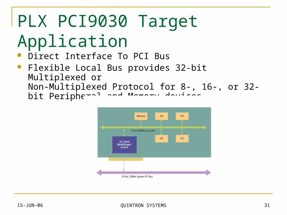
PLX PCI9030 Target Application Direct Interface To PCI Bus Flexible Local Bus provides 32-bit Multiplexed or
Non-Multiplexed Protocol for 8-, 16-, or 32-bit Peripheral and Memory devices

15-JUN-06 QUINTRON SYSTEMS 32
PLX9030 Architecture
Flexible I/O Address Encoding for 8 or 16 Bit Data Buses using “Dynamic Data Bus Width Control Logic”.
Lower Address Bits Derived from Byte Lanes

15-JUN-06 QUINTRON SYSTEMS 33
Byte Lanes: Local Byte Enables LBE[3:0] 16-Bit Transfer
8 X 256MEMORY
LD[7:0]LA7
LA6
LA5
LA4
LA3
LA2
LBE1#
A7
A6
A5
A4
A3
A2
A1
A0
8 X 256MEMORY
LD[15:8]LA7
LA6
LA5
LA4
LA3
LA2
LBE1#
A7
A6
A5
A4
A3
A2
A1
A0
EN#
EN#
LBE3#
CS#
LBE0#
16-BIT X 256 DATA DECODINGNON-MULTIPLEXED MODE
(PLX-9030)LBE[3:0]# Encoding
LA8
LA8

15-JUN-06 QUINTRON SYSTEMS 34
Byte Lanes: Local Byte Enables LBE[3:0] 8-Bit Transfer
8 X 256MEMORY
LD[7:0]
LA7
LA6
LA5
LA4
LA3
LA2
LBE1#
LBE0#
A7
A6
A5
A4
A3
A2
A1
A0
EN#CS#

15-JUN-06 QUINTRON SYSTEMS 35
PLX9030 Synopsis & Availability
Mature Product (Introduced in 1999) Used Throughout the Industry to interface
Target Agents to PCI-32 Low Cost PCI9030A60PI F (F = RoHS)
=$20.70 EA. (Quantities = 100) 12-13 WEEK Lead Time
Hardware & Software Development Kits and Reference Designs Available

PCI-104 Review
By: Robert Rappaport
Presentation Available for download at: ftp.sierratech.net/pub/QUINTRON/