introduction - research.utwente.nl chapter presents an ... the use of electrostatic actuation and...
TRANSCRIPT

1
Chapter One
INTRODUCTION
This chapter presents an introduction into the field of micromechanics. A summary ispresented of transduction principles that are applied in microactuators. The importantclass of electrostatic microactuators is described and a survey of micromechanicalfabrication techniques is given. Finally the scope and the outline of this thesis aresummarised.
1.0 MICROMECHANICS
The advances made by silicon IC technology have led to the application ofmicroelectronic devices and components in a wide range of new areas. Thetrends for microelectronic systems are characterised by increasingminiaturisation, decreasing costs with respect to function, and increasingcomplexity and performance. Various transducers such as sensors andactuators are required to enable electronic systems to interface with theirenvironment. Untill now transducers have mainly been fabricated usingconventional fine mechanics. This is a limiting factor for further systemintegration with respect to miniaturisation, performance and price. Thereforean increasing demand for new transducers based on IC fabrication and otherthin film technologies can be observed.
Micromachining techniques use silicon as a mechanical material due to itsgood mechanical properties and exploit the highly developed technology ofintegrated circuits for the fabrication of mechanical structures with very smalldimensions. The use of silicon as a base material allows the monolithicintegration of mechanical structures with electronic circuitry on the same chip.This enables the fabrication of sophisticated microsystems with totally newtypes of applications and performance.
Due to fundamental scaling properties, the microworld is dominated bysurface forces such as surface tension and friction. Bulk forces like inertia andweight tend to become insignificant in the small domain. In the presentations

2 Introduction
"There's plenty of room at the bottom" [1.1] and "Infinitesimal machinery"[1.2], dating from respectively 1967 and 1982, R.P. Feynman described thecoming technology of making small things and small scale information. Healready anticipated the sacrificial layer method of making silicon micromotors,the use of electrostatic actuation and the importance of friction and stiction[1.3].
Systems with small dimensions have advantages that include speed,accuracy and sensitivity. Improvements with respect to reproducibility andreliability of micromechanical devices are also a direct consequence of the batchprocessing technique employed in the usual silicon IC manufacturing process.Furthermore, a small system can be built from very expensive materials withdesirable properties as the cost of materials scales at the third power withcharacteristic dimensions. Except for thin film processes, it is quite difficult todetermine alternative means of building the structures used in microfabricatedactuators that involve well characterised and controlled processes.
Micromechanical devices are used for a wide range of applications coveringthe field of sensors, actuators and constructive elements. Sensors are normallyused for transferring information between the electronic and non-electronicworld. Micromechanical sensors are mainly used for the detection ofmechanical properties such as pressure, acceleration, force, position or flow.Beyond this, micromechanical structures are used for applications where smallsize and/or small heat capacity increases the performance of the device withrespect to sensitivity, response time, power consumption, etc. Typical examplesare chemical sensors, temperature sensors and sensors for the detection ofradiation. Up to now, pressure and acceleration sensors are the most advancedmicromechanical devices.
Even though miniaturisation of mechanical systems is often compared tothe miniaturisation of electronics, one should not assume that all mechanicalsystems will benefit from miniaturisation. For many mechanical systems suchas those in the automotive industry, miniaturisation is not practical. However,even in these cases micromechanical devices for sensing and actuation canoften improve the overall performance of the system and are attractive becauseof the batch processing nature of the technology, which produces devices witha low unit cost. However, it should be noted that the overall costs of a finaldevice are also determined by costs such as application specific packaging,bonding and testing. An implicit advantage of the technology is the ability tomake a large number of micromechanical devices on the same substrate. Manyapplications can benefit from the collective operation of a large number of

Microactuators 3
devices. For example a silicon optical display using a large array of individuallyaddressable torsional mirrors.
The world market for these micromechanical devices is expected to grow toabout 10,000 million ECU in the year 2000 [1.4]. Sensors are dominating themarkets, but within this decade actuators will gain importance and areexpected to hold about 40% of the market in the year 2000. Micromechanicaldevices are governing the competitiveness of larger instruments or systems,with a market value of about two orders of magnitude larger, demonstratingthe role of micromechanics as a key technology of this decade. During the pastdecade the need for microactuator technology has been increasinglyemphasised, and recent advances in microactuators are transforming the fieldof solid state tranducers into the field of Micro Electro Mechanical Systems
(MEMS).
1.1 MICROACTUATORS
In contrast to microsensors, research on microfabricated actuators(microactuators) has been largely neglected. The realisation ofmicromechanical actuators is generally handicapped by the fact that silicondoes not exhibit a direct electromechanical actuation mechanism of itself.Electromechanical signal conversion has to be achieved, therefore, viasecondary materials and/or system properties.
Actuators are used for the transformation of non-mechanical input energyinto mechanical output energy. Microactuators can be divided into two classes:mechanisms and deformable microstructures. Mechanism-type actuators suchas micromotors provide displacement and force through rigid-body motionwhereas deformable microstructures such as beams and diaphragms providedisplacement and force through mechanical deformations. An importantissue, especially related to mechanism type of actuators, is microtribology.
An important step in the progress of microactuator technology is thedevelopment of actuation forms that can be implemented with the materialsand processing technologies of silicon microelectronics. In addition, theactuation should be powered and controlled electrically in order to becompatible with microelectronics. Despite these stringent requirements, avariety of physical phenomena for microactuator applications have beendemonstrated [1.5-1.15].

4 Microactuators
Microactuators employing electrostatic [1.16-1.90], piezoelectric [1.91-1.103],and magnetic [1.104-1.119] effects have been realised. Also microactuators basedon thermal effects such as thermal expansion and bi-metal effects [120-131],thermopneumatic and phase change actuators [1.132-1.141] as well as ShapeMemory Alloy actuators [1.142-1.146] have been fabricated. Beside thesemethods other mechanisms like fluid actuated devices [1.147-1.152], giantmagnetostrictive alloy actuators [1.153-1.155], electrochemical actuators [1.156]and mechanochemical actuators [1.157] have also been used. The mostcommonly used microactuation mechanisms are electromagnetic or thermal.The most notable thermal microactuation methods are bi-metallic,thermopneumatics and SMA and the most important electromagneticmicroactuation methods are electrostatic, piezoelectric and magnetic.
The force or torque produced by a specific actuator is equal to its spatial rateof energy conversion. Assuming that equivalent spatial rates can be obtainedby the different actuation mechanisms, a comparison of available stored energyprovides a reasonable metric for comparison of force and torque. Other factorssuch as down scaling, speed, power consumption, material issues, fabricationtechnology, size, integration and application must also be considered whencomparing different microactuation methods. Each actuation principle has itsown advantages and disadvantages. The choice and the optimisation should bemade according to the requirements and applications. Some generalconsiderations will be discussed here which are restricted to thermal andelectromagnetic actuators.
Although heating and cooling rates increase with decreasing dimensions, ingenerally thermal microactuators have a slow response time and a higherpower consumption compared to electromagnetic microactuators. Thermalactuation methods are generally more suited for deformable types ofmicroactuators and have been shown to be useful in large deflection and largeforce actuator applications.
As previously mentioned, important electromagnetic microactuationmethods are electrostatic, piezoelectric and magnetic actuation. Magnetic andelectrostatic actuation are often employed in microactuators and have beencompared by many authors [1.158-1.162]. Although with superconductingmagnets very high magnetic fields are feasible, magnetic induction is normallylimited to about 1.5 T because of magnetic saturation. The electric breakdownlimit in air increases drastically from 3.106 V/m for macroscopic air gaps to 108
for air gaps on the order of a micrometer. As a result the stored energydensities of magnetic and electrostatic actuation are comparable at micron

Electrostatic microactuators 5
scales and are of the order of 105 to 106 J/m3.Efficiency considerations favour electrostatic microactuators over magnetic
microactuators. Static excitation of magnetic actuators requires static currentsthrough its windings, leading to persistent conduction losses. However staticexcitation of electrostatic actuators requires static voltages across gaps whichcan be essentially lossless. This argument holds as the speed of the actuatorincreases until reactive power dominates the electrical excitation of theactuator. This should occur at comparable speeds in both types of actuators.Most magnetic actuators contain magnetisable material that will exhibitincreasing eddy-current and hysteresis losses as the speed increases.
Typical piezoelectric materials and thin films used in microactuatortechnology are quartz, zinc oxide (ZnO), lead zirconate titanate (PZT), andpolyvinylidene fluoride (PVDF). High energy densities are feasible with PZT.Piezoelectric actuation has been used for deformable types of structures. Butpiezoelectric motors have also been fabricated that are based on travellingwave ultrasonics, impact drive mechanisms and stick-slip or walkingmechanisms where fast vibratory motions are transformed into a slowermacroscopic motion.
Generally, the most important factors that have to be considered are thechoice of materials and microfabrication techniques. For electrostatic actuators,conductors and insulators are easily available in IC technology, while magneticor piezoelectric materials are not readily obtainable in integrated circuitprocessing. Furthermore, piezoelectric materials and soft magnetic materials,hard magnetic materials and magnetic circuit components such as coils aremore difficult to implement in micromachining processes. As a result, manyelectrostatically driven actuators have been developed and realised, and onlylittle actuators have been fabricated employing magnetic or piezoelectricactuation.
Research on microactuators is developing fast and much progress has beenmade in recent years. One is at the point where micromechanisms are startingto walk [1.50, 1.79, 1.163], swim [1.164] and fly [1.115, 1.165, 1.166].
1.2 ELECTROSTATIC MICROACTUATORS
Electrostatic actuators have a long history dating back to the 18th centurywhen several types of electrostatic motors were built [1.167]. In macroscopicdevices electrostatic forces are relatively small and high driving voltages are

6 Introduction
needed. For this reason, electrostatic actuation is rarely used in macroscopicdevices. In contrast, electrostatic actuation is attractive for microactuators asexplained earlier [1.158-1.162]. One of the first applications of electrostatic forcesin silicon micromechanism was to bend or tilt micro beams for use inmechanical filters, light modulator arrays and electromechanical switches[1.168].
Electrostatic actuation is based upon attractive or repulsive forces betweenpositive and negative charges. In fig. 1 two conducting parallel plates areshown with equal but opposite charges. The vectors indicate the electric forcesacting between the upper and the lower plate. These attractive forces tend toalign and pull the plates together. A mechanically unrestrained conductingbody with net charge, in an electric field created by stationary externalconductors each with fixed total charge, can never be in stable equilibrium.Therefore, a mechanically restraining structure is necessary, like a spring orbearing, in order to obtain a stable electrostatic actuator.
-
++
++
++
++
++
++
++
+-
--
--
-
--
-
--
-
--
-
Fig. 1.1 Electric forces induced by offset charge distributions.
Several types of electrostatic actuators can be distinguished by the manner inwhich the rotor charge distribution is defined. For example: a permanentelectret motor has a fixed charge embedded in the rotor. An electric hysteresismotor uses hysteresis in the polarisability of the rotor to maintain the properphase difference between the rotor and stator charge distributions. An electricinduction motor is designed in such a way that the charge distribution isinduced in a resistive rotor by the stator charge distribution with the properspatial phase difference maintained by charge relaxation. The rotor chargedistribution can also be induced by the stator charge distribution, but itsdefinition and offset can be obtained by geometrical variations in the stator torotor gap like, for example, saliencies in the highly conductive rotor. Motorsbased on this principle are called variable capacitance motors.
Electrostatic actuators can be charge or voltage driven. The driving conditionis not irrespective with regard to the actuator behaviour. The voltage is in

Fabrication technologies 7
many cases the most suitable choice for the independent variable because theelectrodes define equipotential surfaces making the voltage independent ofposition. Constant charge conditions can only be guaranteed at terminal level,i.e. global and not local. Constant voltage conditions at terminal level on theother hand also imply constant voltage conditions locally. The electrostaticforce or torque acting on a charged body can be calculated from the spatialderivative of the electrostatic energy at constant charge or from the spatialderivative of the electrostatic co-energy at constant voltage.
A variety of electrostatic microactuators employing arrangements such asparallel plate capacitors, interdigitated finger or comb structures androtor/stator designs have been fabricated.
1.3 FABRICATION TECHNOLOGIES
The processing technology of IC's generally consists of a sequence of planarprocesses modifying the properties of the semiconductor material and thesurface topology within a few micron's depth. The fabrication of mostmicromechanical devices relies on a three dimensional structuring of thesubstrate material and or secondary layers deposited on top of the originalplane.
Probably the oldest micromachining technique is called bulkmicromachining [1.168-1.170]. For bulk micromachining, anisotropic dry andwet etching processes are applied to structure the monocrystalline bulkmaterial. Several silicon etchants, like KOH, EDP and NH4OH, exhibit adependency of the etch rate on the crystallographic orientation of single crystalsilicon. Using silicondioxide, silicon nitride or metals like e.g. Cr, Au, Ag andPt as a mask well defined grooves, cavities and mesas bounded by sloweretching (111) planes can be etched. Furthermore silicon dopants and electricpotential can be used to create etch stop layers. Together with wafer-to-waferbonding techniques, like anodic bonding and direct bonding, several wafers canbe stacked together which results in an increased versatility of the devices thatcan be fabricated [1.171, 1.172].
In addition to bulk micromachining, surface micromachining techniqueshave been developed [1.173-1.179]. In surface micromachining structural partsare embedded in layers of a sacrificial material during the fabrication process.The sacrificial material is then etched or dissolved in a chemical etchant thatdoes not attack the structural parts. Polysilicon surface micromachining using

8 Introduction
doped or undoped polysilicon as the structural material and silicon dioxide orPSG as the sacrificial layer is the most widely used surface micromachiningtechnique.
Another important fabrication method is LIGA [1.180-1.183]. LIGAtechniques are based on X-ray exposure and development of thick resist layers,and subsequent electroplating of metal layers to form the micromechanicalstructures. After stripping of the resist either a final metal structure or a metalmould insert for subsequent replication processes like injection moulding isobtained. With LIGA techniques very high aspect ratio structures can beobtained with thicknesses ranging up to about one mm and lateral dimensionsdown to the submicron range.
Besides LIGA other moulding techniques based on UV exposure emergedwhich are characterised by a lower aspect ratio of around 10, a structuralthickness of up to about 100 µm and less dimensional control [1.184-1.189].
Dry fabrication techniques like SCREAM [1.190, 1.191], SIMPLE [1.192] andBSM [1.194] have also been used to fabricate micromechanical structures. Theseare based upon patterning of the silicon wafer by deep anisotropic etching ofsilicon, subsequent sidewall passivation and release of the structures by dryisotropic underetching of the silicon wafer.
Combinations of previous techniques are also possible. For examplesacrificial layers are also employed in the LIGA technique and recently 3Dsurface micromachining techniques (HEXSIL) have also been demonstrated.Here small and deep etching grooves in the silicon wafer are used as a mold forthe sacrificial layer and are subsequently filled with the structural material[1.194]. After removal of the sacrificial layer 3D structures are obtained and thesilicon mold can be recycled for further use. Other examples are a combinationof bonding and deep dry etching techniques [1.195, 1.196], the dissolved waferprocess where dry anisotropic etching, highly boron doped etch stoptechniques, bonding, and wet etching are employed [1.197, 1.198] and DEEMOwhere deep dry etching of silicon is employed to fabricate a mould for multiplereplications [1.199].
1.4 OUTLINE OF THIS THESIS
Conventional microstructures, such as cantilever beams, bridges anddiaphragms, are able to move only a limited amout of micrometersperpendicular to the plane of the substrate. This restrained travel in one degree

Outline of this thesis 9
of freedom has restricted existing microactuators to small motion applications.A flexible microactuator technology requires structures that have unrestrainedmotion in at least one degree of freedom. Surface micromachining techniquesprovide this possibility. At the onset of this work only bulk micromachiningwas used at the MESA Research Institute. A surface micromachiningtechnology needed to be developed and implemented within the existingcleanroom facilities. Polysilicon surface micromachining is the bestdocumented surface micromachining technique to date and has been used inthis work. Two central issues in surface micromachining are: theunderstanding and control of the mechanical properties of microstructuralfilms and the release of the microstructure, for example by wet etching,followed by the drying and surface passivation of the microstructure. Anotherimportant fabrication aspect is dimensional control of fabricated structures.The fabrication of electrostatic actuators demands small gaps and compliant orhigh aspect ratio polysilicon microstructures. This requires anisotropic etchingtechniques of polysilicon. It was therefore necessary to develop a dryanisotropic etching process based on fluorine chemistry. The resulting surfacemicromachining technology has been used to fabricate a variety ofelectrostatically driven actuators.
Current microactuation techniques provide either large motion or high forceand torque. For many practical applications both characteristics are needed. Inorder to extend the possibilities of electrostatic actuators emphasis was given tothe design and development of electrostatic actuators that provide relativelylarge forces and displacements.
In this first chapter a general introduction to micromachining technologyand microactuators has been given. Chapters 2-4 deal with technologicalaspects and in chapters 5-9 emphasis is given to device design and performanceof different electrostatic actuators. General conclusions are drawn in chapter 10.Chapter 2 presents an overview of surface micromachining technology withemphasis on polysilicon surface micromachining. The basic fabrication stepsare described and material requirements are discussed. Methods to determinethe mechanical properties of thin films are summarised. The control ofpolysilicon mechanical properties, etch characteristics of silicon dioxide inhydrofluoric acid and techniques to prevent stiction of surface micromachinedstructures are described. Examples of basic surface micromachining processesand some special techniques are given.
In chapter 3 the mechanisms causing stiction of polysilicon structuresfabricated by surface micromachining techniques are investigated. A simplified

10 Introduction
model is used to show that capillary forces are responsible for bringingmicromechanical structures into contact with the underlying substrate.Experimental results obtained from drying experiments are given andcompared with the theory. Measured adhesion energies of stickingmicrobridges after drying are compared with various adhesion mechanisms inorder to reveal the origin of the forces.
Chapter 4 describes a study of reactive ion etching of silicon, usingSF6/O2/CHF3, plasmas in an RF parallel plate system. Surface responsemethodology is used to examine etch rate, selectivity, anisotropy and self-biasvoltage as a function of SF6 flow, O2 flow, CHF3 flow, pressure and the RFpower. The effects of the variables on the measured responses are discussed.Examples of anisotropic etching of high aspect ratio structures with smoothetch surfaces are given.
In chapter 5 the design and performance of a curved electrode actuator ispresented. Its operation is based on the deformation of a movablemicromechanical structure which is deflected by electrostatic forces along afixed curved electrode. The behaviour of this type of actuator is studied byusing cantilever beam structures. A theoretical description of the staticbehaviour of a deformable cantilever beam that is forced into contact with arigid structure by means of electrostatic forces is given. Modelling of the staticbehaviour is done by a simplified model based on energy methods and by 3Dcoupled electromechanical simulations using CoSolve-EM. Experiments areperformed in order to verify theoretical results.
Chapter 6 presents the design, fabrication and experimental results of lateralcomb-drive actuators for large displacements at low driving voltages. Severalsuspension designs are compared with respect to large deflection behaviour.The electromechanical behaviour of comb-drive actuators is considered withrespect to large deflection behaviour. Static and dynamic properties aredetermined experimentally and are compared with theory.
Chapter 7 presents the design, modelling, fabrication and first performancecharacteristics of electrostatically driven axial-gap polysilicon wobble motors.Aspects like the gear ratio, torque generation, excitation schemes and torquecoverage, normal forces, friction, rotor kinetics and dynamical behaviour areaddressed. The motor performance is characterised by gear ratio measurementsand measuring starting and stopping voltages.
In chapter 8 a surface micromachining process is presented that has beenused for the fabrication of electrostatic microactuators which are connectedwith eachother and linked to other movable microstructures by integrated gear

References 11
linkages. The gear linkages consist of rotational and linear gear structures andthe electrostatic microactuators include curved electrode actuators, comb driveactuators and axial gap wobble motors. It is a first step towards mechanicalpower transmission in micromechanical systems.
In chapter 9 basic design issues and a fabrication process based on surfacemicromachining techniques for electrostatically driven vacuum encapsulatedpolysilicon resonators are presented. Experimental results, including anadmittance plot of the one-port resonator and a plot indicating the dependenceof the Q-factor on the resonator geometry and ambient pressure are presented.
Finally in chapter 10 general conclusions are drawn and suggestions forfurther research are given.
REFERENCES
[1.1] R.P. Feynman, There's plenty of room at the bottom, Journal of microelectromechanicalsystems, Vol. 1, 1992, pp. 60-66.
[1.2] R.P. Feynman, Infitesimal machinery, Journal of microelectromechanical systems, Vol. 2,1993, pp. 4-14.
[1.3] S.D. Senturia, Feynman revisited, Proc. IEEE Micro Electro Mechanical Systems, Oiso,Japan, Jan. 25-28, 1994, pp. 309-312.
[1.4] G. Tschulena, Micromechanics business opportunities, Proc. 3rd Int. Conf. on micro electro,opto, mechanic systems and components, Berlin, October 21-23, 1992, pp. 51-57.
[1.5] R.S. Muller, From IC's to microstructures: materials and technologies, Proc. IEEE MicroRobots and Teleoperators Workshop, Hyannis, MA, U.S.A., Nov. 9-11, 1987. , pp. 1-5.
[1.6] W.S.N. Trimmer, Microrobots and Micromechanical systems, Sensors and Actuators, 19,1989, pp. 267-287.
[1.7] W. Benecke, Silicon micromachining for microsensors and microactuators, MicroelectronicEngineering, Vol. 11, 1990, pp. 73-82.
[1.8] R. S. Muller, Microdynamics, Sensors and Actuators, A21-A23, 1990, pp. 1-8.[1.9] K.D. Wise, Integrated microelectromechanical systems: A perspective on MEMS in the
90s, Proc. IEEE Micro Electro Mechanical Systems, Nara, Japan, Jan. 30-Feb. 2, 1991, pp.33-38.
[1.10] H. Fujita and K.Gabriel, New opportunities for micro actuators, Proc. 6th Int. Conf. Solid-State Sensors and Actuators (Transducers '91), San Fransisco, CA, USA, June 24-27, pp. 14-20.
[1.11] W. Benecke, Silicon microactuators: activation mechanisms and scaling problems, Proc.6th Int. Conf. Solid-State Sensors and Actuators (Transducers '91), San Fransisco, CA,USA, June 24-27, pp. 46-50.
[1.12] P. Dario, R. Valleggi, M.C. Carrozza, M.C. Montesi and M. Cocco, Microactuators formicrorobots: a critical survey, J. Micromech. Microeng. , Vol. 2, 1992, pp. 141-157.
[1.13] M. Mehregany, Microelectromechanical Systems, IEEE Circuits and Devices Magazine,Vol. 9, 1993, pp. 14-22.
[1.14] T. Hayashi, Micromechanism and their characteristics, Proc. IEEE Micro ElectroMechanical Systems, Oiso, Japan, Jan. 25-28, 1994, pp. 39-44.
[1.15] H. Fujita, Recent progress of microactuators and micromotors, Microsystem Technologies,Vol. 1, 1995, pp. 93-97.

12 Introduction
[1.16] H. C. Nathanson, W. E. Newell, R. A. Wickstrom and J.R. Davis jr., The resonant gatetransistor, IEEE Trans. on El. Dev., ED-14 (1967), pp. 117-133.
[1.17] H.Fujita and A. Omodaka, The fabrication of an electrostatic linear actuator by siliconmicromachining, IEEE Trans. on El. Devices, Vol. 35, 1988, pp. 731-734.
[1.18] Electrostatic-comb drive of lateral polysilicon resonators, W.C. Tang, T.C.H. Nguyen,M.W. Judy and R.T. Howe, Proc. 5th Int. Conf. Solid-State Sensors and Actuators(Transducers '89), Montreux, Switzerland, June 25-30, 1989, pp. 328-331.
[1.19] Y.C. Tai, L.S. Fan and R.S. Muller, IC-processed micro-motors: design, technology andtesting, Proc. IEEE Micro Electro Mechanical Systems, Salt Lake City, Utah, U.S.A., Feb.20-22, 1989, pp. 1-6.
[1.20] R. Jebens, W. Trimmer and J. Walker, Microactuators for aligning optical fibers, Sensorsand Actuators, 20, 1989, pp. 65-73.
[1.21] M. Mehregany, S.F. Bart, L.S. Tavrow, J.H. Lang, S.D. Senturia and M.F. Schlecht, Astudy of three microfabricated variable-capacitance motors, Proc. 5th Int. Conf. Solid-State Sensors and Actuators (Transducers '89), Montreux, Switzerland, June 25-30, 1989,pp. 173-179.
[1.22] L.S. Tavrow, S.F. Bart, J.H. Lang and M.F. Schlecht, A LOCOS process for an electrostaticmicrofabricated motor, Proc. 5th Int. Conf. Solid-State Sensors and Actuators(Transducers '89), Montreux, Switzerland, June 25-30, 1989, pp. 893-898.
[1.23] R. Mahadevan, K.J. Gabriel and Mehregany, Application of electric microactuators tosilicon micromechanics, Proc. 5th Int. Conf. Solid-State Sensors and Actuators(Transducers '89), Montreux, Switzerland, June 25-30, 1989, pp. 219-225.
[1.24] R.A. Brennen, M.G. Lim, A.P. Pisano and A.T. Chou, Large displacement linear actuator,Proc. IEEE Solid-State Sensors and Actuators Workshop, Hilton Head Island, SC, U.S.A.June 4-7, 1990, pp. 135-139.
[1.25] S. Egawa and T. Higuchi, Multi-layered electrostatic film actuator, Proc. IEEE MicroElectro Mechanical Systems, Napa Valley, CA, U.S.A., Feb. 11-14, 1990, pp. 166-171.
[1.26] K.S.J. Pister, R.S. Fearing and R.S. Howe, A planar air levitated electrostatic actuatorsystem, Proc. IEEE Micro Electro Mechanical Systems, Napa Valley, CA, U.S.A., Feb. 11-14, 1990, pp. 67-71.
[1.27] W.C. Tang, M.G. Lim and R.T. Howe, Electrostatically balanced comb drive for controlledlevitation, Proc. IEEE Solid-State Sensors and Actuators Workshop, Hilton Head Island,SC, U.S.A. June 4-7, 1990, pp. 23-27.
[1.28] R.A. Brennen, A.P. Pisano and W.C. Tang, Multiple mode micromechanical resonators,Proc. IEEE Micro Electro Mechanical Systems, Napa Valley, CA, U.S.A., Feb. 11-14, 1990,pp. 9-14.
[1.29] S. Nakagawa, S. Shoji and M. Esashi, Micromachined silicon microvalve, Proc. IEEEMicro Electro Mechanical Systems, Napa Valley, CA, U.S.A., Feb. 11-14, 1990, pp. 95-98.
[1.30] P.L. Bergstrom, T. Tamagawa and D.L. Polla, Design and fabrication of micromechanicallogic elements, Proc. IEEE Micro Electro Mechanical Systems, Napa Valley, CA, U.S.A.,Feb. 11-14, 1990, pp. 15-20.
[1.31] M. Mehregany, P. Nagarkar, S.D. Senturia and J.H. Lang, Operation of microfabricatedharmonic and ordinary side-drive motors, Proc. IEEE Micro Electro Mechanical Systems,Napa Valley, CA, U.S.A., Feb. 11-14, 1990, pp. 1-8.
[1.32] M. Mehregany, S.M. Philips, E.T. Hsu and J.H. Lang, Operation of harmonic side-drivemicromotors studied through gear ratio measurements, Proc. 6th Int. Conf. Solid-StateSensors and Actuators (Transducers '91), San Fransisco, CA, USA, June 24-27, pp. 59-62.
[1.33] L.S. Tavrow, S.F Bart and J.H. Lang, Operational characteristics of microfabricatedelectric motors, Proc. 6th Int. Conf. Solid-State Sensors and Actuators (Transducers '91),San Fransisco, CA, USA, June 24-27, pp. 877-881.
[1.34] N. Takeshima, K. J. Gabriel, M. Ozaki, J. Takahasji, H. Horiguchi and H. Fujita,Electrostatic parallelogram actuators, Proc. 6th Int. Conf. Solid-State Sensors andActuators (Transducers '91), San Fransisco, CA, USA, June 24-27, 1991, pp. 63-66.
[1.35] P. Gunther, SiO2 electrets for electric-field generation in sensors and actuators, Sensorsand Actuators, Vol. A32, 1992, pp. 357-360.

References 13
[1.36] K.J. Gabriel, O. Tabata, K. Shimaoka, S. Sugiyama and H. Fujita, Surface-normalelectrostatic/pneumatic actuator, Proc. IEEE Micro Electro Mechanical Systems,Travemünde, Germany, Feb. 4-7, 1992, pp. 128-132.
[1.37] U. Breng, T. Gessner, C. Kaufmann, R. Kienscherf and J. Markert, Electrostaticmicromechanic actuators, Journal of Micromechanics and Microengineering, Vol. 2, 1992,pp. 256-262.
[1.38] V.P. Jaecklin, C. Linder, N.F. de Rooy and J.M. Moret, Micromechanical comb actuatorswith low driving voltage, J. Micromech. Microeng., Vol. 2, 1992, pp. 250-255.
[1.39] T. Hirano, T. Furuhata, K.J. Gabriel and H. Fujita, Design, fabrication and operation ofsub-micron gap electrostatic comb-drive actuators, Journal of MicroelectromechanicalSystems, Vol. 1, No. 1, March 1992, pp. 52-59.
[1.40] K. Sato and M. Shikida, Electrostatic film actuator with large vertical displacement,Proc. IEEE Micro Electro Mechanical Systems, Travemunde, Germany, February 4-7, 1992,pp. 1-5.
[1.41] C.J. Kim, A.P. Pisano and R.S. Muller, Overhung electrostatic micro gripper, Journal ofMicroelectromechanical Systems, Vol. 1, No. 1, March 1992, pp. 31-36.
[1.42] J. Branebjerg and P. Gravesen, A new electrostatic actuator providing improved strokelength and force, Proc. IEEE Micro Electro Mechanical Systems, Travemunde, Germany,February 4-7, 1992, pp. 6-11.
[1.43] A.P. Lee and A.P. Pisano, Polysilicon angular microvibromotors, Journal ofMicroelectromechanical Systems, Vol. 1, No. 2, June 1992, pp. 70-76.
[1.44] W.C. Tang, M.G. Lim and R.T. Howe, Electrostatic comb drive levitation and controlmethod, Journal of Microelectromechanical Systems, Vol. 1, No. 4, Dec. 1992, pp. 170-178.
[1.45] U. Breng, C. Kaufmann, R. Kiehnscherf, J. Markert and M. Rauch, Electrostaticmicromechanic actuators, 3rd Int Conf. on New Actuators (Actuator '92), Bremen,Germany, 24-26 June, 1992, pp. 177-182.
[1.46] V.P. Jaecklin, C. Linder, N.F. de Rooij, J.M. Moret, R. Bischot and F. Rudolf, Novelpolysilicon comb actuators for xy-stages, Proc. IEEE Micro Electro Mechanical Systems,Travemünde, Germany, Feb. 4-7, 1992, pp. 147-149.
[1.47] N. Tirole, D. Hauden, P. Blind, M. Froelicher and L. Gaudriot, 3D silicon electrostaticmicroactuator, Journal of Micromechanics and Microengineering, Vol. 3, 1993, pp. 155-157.
[1.48] M. Yamaguchi, S. Kawamura, K Minami and M Esashi, Distributed electrostatic microactuator, Proc. IEEE Micro Electro Mechanical Systems, Fort Lauderdale, Florida, U.S.A.,February 7-10, 1993, pp. 18-23.
[1.49] V.P. Jaecklin, C. Linder, N.F. de Rooij, Comb actuators for xy-microstages, Sensors andActuators, Vol. A 39, 1993, pp. 83-89.
[1.50] T. Akiyama and K. Shono, Controlled stepwise motion in polysilicon microstructures,Journal of Microelectromechanical Systems, Vol. 2, No. 3, Sept. 1993, pp. 106-110.
[1.51] T. Niino, S. Egawa and T. Higuchi, High-power and high-efficiency electrostaticactuator, Proc. IEEE Micro Electro Mechanical Sytems, Fort Lauderdale, Fl, U.S.A.,February 7-10, 1993, pp. 236-241.
[1.52] T. Hirano, T. Furuhata and H. Fujita, Dry released Nickel micromotors and their frictioncharacteristics, Proc. 7th Int. Conf. Solid-State Sensors and Actuators (Transducers '93),Yokohama, Japan, June 7-10, pp. 80-83.
[1.53] L.Y. Chen, E.J.P. Santos and N.C. MacDonald, Serial-parallel isolated capacitivemicroactuators, Proc. 7th Int. Conf. Solid-State Sensors and Actuators (Transducers '93),Yokohama, Japan, June 7-10, pp. 84-87.
[1.54] G. Fuhr and B. Wagner, Surface-charge induction micromotors with two aluminium rotorsisolated by SiO2, Proc. 7th Int. Conf. Solid-State Sensors and Actuators (Transducers '93),Yokohama, Japan, June 7-10, pp. 88-92.
[1.55] A.P. Lee, A.P. Pisano and D.J. Nikkel, Polysilicon linear microvibromotors, Proc. 7th Int.Conf. Solid-State Sensors and Actuators (Transducers '93), Yokohama, Japan, June 7-10,pp. 46-49.

14 Introduction
[1.56] T. Matsubara, M. Yamaguchi, K. Minami and M. Esashi, Stepping electrostaticmicroactuator, Proc. 7th Int. Conf. Solid-State Sensors and Actuators (Transducers '93),Yokohama, Japan, June 7-10, pp. 50-53.
[1.57] V.P. Jaecklin, C. Linder, N.F. deRooij, J.M. Moret and R. Vuilleumier, Opticalmicroshutters and torsional micromirrors for ligth modulator arrays, Proc. IEEE MicroElectro Mechanical Systems, Ford Lauderdale, Florida, U.S.A., Feb. 7-10, 1993, pp. 124-127.
[1.58] V.P. Jaecklin, C. Linder, J. Brugger and N.F. deRooij, Mechanical and optical propertiesof surface micromachined torsional mirrors in silicon, polysilicon and aluminum, Proc. 7thInt. Conf. Solid-State Sensors and Actuators (Transducers '93), Yokohama, Japan, June 7-10, pp. 958-961.
[1.59] K. Aratani, P.J. French, P.M. Sarro, R.F. Wolffenbuttel and S. Middelhoek, Surfacemicromachined tunable interferometer array, Proc. 7th Int. Conf. Solid-State Sensors andActuators (Transducers '93), Yokohama, Japan, June 7-10, pp. 678-681.
[1.60] J.B. Sampsell, The digital micromirror device and its application to projection displays,Proc. 7th Int. Conf. Solid-State Sensors and Actuators (Transducers '93), Yokohama,Japan, June 7-10, pp. 24-27.
[1.61] E. Obermeier, J. Lin and V. Schlichting, Design and Fabrication of an electrostaticallydriven micro-shutter, Proc. 7th Int. Conf. Solid-State Sensors and Actuators (Transducers'93), Yokohama, Japan, June 7-10, pp. 132-137.
[1.62] O. Tabata, R. Asahi, N. Fujitsuka, M. Kimura and S. Sugiyama, Electrostatic drivenoptical chopper using SOI, Proc. 7th Int. Conf. Solid-State Sensors and Actuators(Transducers '93), Yokohama, Japan, June 7-10, pp. 124-127.
[1.63] J. Bernstein, A.T. King, A. Kourepenis, P. Maciel and M. Weinberg, A micromachinedcomb-drive tuning fork rate gyroscope, Proc. IEEE Micro Electro Mechanical Systems, FordLauderdale, Florida, U.S.A., Feb. 7-10, 1993, pp. 143-148.
[1.64] J.W. Judy, T. Tamagawa and D.L. Polla, Surface-machined micromechanical membranepump, Proc. IEEE Micro Electro Mechanical Systems, Ford Lauderdale, Florida, U.S.A.,Feb. 7-10, 1993, pp. 182-186.
[1.65] S.M. Bobbio, M.D. Kellam, B.W. Dudley, S. Goodwin-Johansson, S.K. Jones, J.D. Jacobson,F.M. Tranjan and T.D. DuBois, Integrated force arrays, Proc. IEEE Micro ElectroMechanical Systems, Ford Lauderdale, Florida, U.S.A., Feb. 7-10, 1993, pp. 149-154.
[1.66] J. Schimkat, L. Kiesewetter, H.J. Gevatter, F. Arndt, A. Steckenborn and H.F. Schlaak,Moving wedge actuator: An electrostatic actuator for use in microrelay, Proc. 4th Int.Conf. and Exhibition on Micro Electro, Opto, Mechanical Systems and Components(Actuator '94), Berlin, Germany, October 19-21, 1994, pp. 989-996.
[1.67] H. Guckel, T.R. Christenson, T. Earles, K.J. Skrobis and J. Klein, Processing and designconsiderations for high force output-large throw electrostatic, linear micro actuators, 4thInt Conf. on New Actuators (Actuator '94), Bremen, Germany, 15-17 June, 1994, pp. 105-108.
[1.68] H. Kalb, B. Kowanz, W. Bacher, J. Mohr and R. Ruprecht, Electrostatically driven linearstepping motor in LIGA technique, 4th Int Conf. on New Actuators (Actuator '94), Bremen,Germany, 15-17 June, 1994, pp. 83-85.
[1.69] K. Deng and M. Mehregany, Outer-rotor polysilicon wobble micromotors, Proc. IEEE MicroElectro Mechanical Systems, Oiso, Japan, Jan. 25-28, 1994, pp. 269-272.
[1.70] K. Deng, H. Miyajima, V.H. Dhuler, M. Mehregany, S.W. Smith, F.L. Merit and S.Furukawa, The development of polysilicon micromotors for optical scanner applications,Proc. IEEE Solid-State Sensors and Actuators Workshop, Hilton Head Island, SC, U.S.A.,June 13-16, 1994, pp. 234-238.
[1.71] R.B. Apte, F.S.A. Sandejas, W.C. Banyai and D.M. Bloom, Deformable grating ligthvalves for high resolution displays, Proc. IEEE Solid-State Sensors and ActuatorsWorkshop, Hilton Head Island, SC, U.S.A., June 13-16, 1994, pp. 1-6.
[1.72] P.Y. Chen and R.S. Muller, Microchopper-modulated IR microlamp, Proc. IEEE Solid-State Sensors and Actuators Workshop, Hilton Head Island, SC, U.S.A., June 13-16, 1994,pp. 239-242.

References 15
[1.73] C. W. Stroment, D. A. Borkholder, V. A. Westerlind, J. W. Suh, N. I. Maluf and G. T. A.Kovacs, Dry-released process for aluminum electrostatic actuators, Proc. Solid-StateSensor and Actuator Workshop, Hilton Head Island, SC, U. S. A., June 13-16, 1994, pp. 95-98.
[1.74] M. Fischer, H. Graaf and W. von Münch, Electrostatically deflectable polysilicontorsional mirrors, Sensors and Actuators, Vol. A 44, 1994, pp. 83-89.
[1.75] R. Zengerle, S. Kluge, M. Richter and A. Richter, A bidirectional silicon micropump, Proc.IEEE Micro Electro Mechanical Systems, Amsterdam, The Netherlands, Jan. 29-Feb. 2,1995, pp. 19-24.
[1.76] A.A. Yasseen, S.W. Smith, M. Mehregany and F.L. Merat, Diffraction grating scannersusing polysilicon micromotors, Proc. IEEE Micro Electro Mechanical Systems, Amsterdam,The Netherlands, Jan. 29-Feb. 2, 1995, pp. 175-180.
[1.77] P.F. Indermuhle, V.P. Jaecklin, J. Brugger, C. Linder, N.F. De Rooij and M. Binggeli, AFMimaging with an xy-micropositioner with integrated tip, Sensors and Actuators, A47,1995, pp. 562-565.
[1.78] A. Selvakumar, K. Najafi. W.H. Juan and S. Pang, Vertical comb array microactuators,Proc. IEEE Micro Electro Mechanical Systems, Amsterdam, The Netherlands, Jan. 29-Feb.2, 1995, pp. 43-47.
[1.79] T. Akiyama and H. Fujita, A quantitative analysis of scratch drive actuator usingbuckling motion, Proc. IEEE Micro Electro Mechanical Systems, Amsterdam, TheNetherlands, Jan. 29-Feb. 2, 1995, pp. 310-315.
[1.80] P. Rangsten, L. Smith, L. Rosengren and B. Hök, Electrostatically excited diaphragmdriven as a loudspeaker, Proc. 8th Int. Conf. Solid-State Sensors and Actuators(Transducers '95), Stockholm, Sweden, June 25-29, 1995, Vol. 1, pp. 430-433.
[1.81] L.S. Fan, S. Woodman, T.C. Reiley, H.H. Zappe and T. Furuhata, Batch fabrication ofmechanical platforms for high density data storage, Proc. 8th Int. Conf. Solid-StateSensors and Actuators (Transducers '95), Stockholm, Sweden, June 25-29, 1995, Vol. 1, pp.434-437.
[1.82] S.G. Adams, F.M. Bertsch, K.A. Shaw, P.G. Hartwell, N.C. MacDonald and F.C. Moon,Capacitance based tunable micromechanical resonators, Proc. 8th Int. Conf. Solid-StateSensors and Actuators (Transducers '95), Stockholm, Sweden, June 25-29, 1995, Vol. 1, pp.438-441.
[1.83] M.T.A. Saif and N.C. MacDonald, A milli Newton micro loading device, Proc. 8th Int.Conf. Solid-State Sensors and Actuators (Transducers '95), Stockholm, Sweden, June 25-29,1995, Vol. 2, pp. 60-63.
[1.84] J. Drake, H. Jerman, B. Lutze and M. Stuber, An electrostatically actuated micro-relay,Proc. 8th Int. Conf. Solid-State Sensors and Actuators (Transducers '95), Stockholm,Sweden, June 25-29, 1995, Vol. 2, pp. 380-383.
[1.85] J.J. Yao and M.F. Chang, A surface micromachined miniature switch fortelecommunications applications with signal frequencies from DC up to 4 GHz, Proc. 8thInt. Conf. Solid-State Sensors and Actuators (Transducers '95), Stockholm, Sweden, June25-29, 1995, Vol. 2, pp. 384-387.
[1.86] J.J. Sniegowski and C. Smith, An application of mechanical leverage to microactuation,Proc. 8th Int. Conf. Solid-State Sensors and Actuators (Transducers '95), Stockholm,Sweden, June 25-29, 1995, Vol. 1, pp. 364-367.
[1.87] E.J. Garcia and J.J. Sniegowski, Surface micromachined microengine as the driver formicromechanical gears, Proc. 8th Int. Conf. Solid-State Sensors and Actuators(Transducers '95), Stockholm, Sweden, June 25-29, 1995, Vol. 2, pp. 365-368.
[1.88] R. Legtenberg, E. Berenschot, M. Elwenspoek and J. Fluitman, Electrostatic curvedelectrode actuators,Proc. IEEE Micro Electro Mechanical Systems, Amsterdam, TheNetherlands, Jan. 29-Feb. 2, 1995, pp. 37-42.
[1.89] R. Legtenberg, E. Berenschot, T. Lammerink and M. Elwenspoek, An electrostatic axialgap wobble motor, Proc. 8th Int. Conf. Solid-State Sensors and Actuators (Transducers'95), Stockholm, Sweden, June 25-29, 1995, Vol. 2, pp. 404-407.

16 Introduction
[1.90] R. Legtenberg, A.W.Groeneveld and M. Elwenspoek, Towards position control ofelectrostatic comb drives, Proc. 6th European workshop on micromachining,micromechanics and microsystems (MME '95), Copenhagen, Denmark, Sept. 3-5, 1995, pp.124-127.
[1.91] H.T.G. van Lintel, F.C.M. van de Pol and S. Bouwstra, A piezoelectric micropump basedon micromachining of silicon, Sensors and Actuators, Vol. 15, 1988, pp. 153-167.
[1.92] W.P. Robbins, D.L Polla, T. Tamagawa, D.E. Glumac and J.W. Judy, Linear motionmicroactuators using piezoelectric thin films, Proc. Int. Conf. on Solid-State Sensors andActuators, (Transducers '91), San Fransisco, CA, U. S. A., June 24-27, 1991, pp. 55-58.
[1.93] A.M. Flynn, L.S. Tavrow, S.F. Bart, R.A. Brooks, D.J. Ehrlich, K.R. Udayakumar and L.E.Cross, Piezoelectric micromotors for microrobots, Journal of microelectromechanicalsystems, Vol. 1, 1992, pp. 44-51.
[1.94] D.E. Brei and J. Blechschmidt, Design and static modeling of a semiconductor polymericpiezoelectric microactuator, Journal of Microelectromechanical Systems, Vol. 1, 1992, pp.106-115.
[1.95] T. Yasuda, I. Shimoyama and H. Miura, Microrobot actuated by a vibrating energy field,Proc. 7th Int. Conf. Solid-State Sensors and Actuators (Transducers '93), Yokohama,Japan, June 7-10, pp. 42-45.
[1.96] G.A. Racine, R. Luthier and N.F. de Rooij, Hybrid ultrasonic micromachined motors, Proc.IEEE Micro Electro Mechanical Systems, Ford Lauderdale, Florida, U.S.A., Feb. 7-10,1993, pp. 128-132.
[1.97] H. Toshiyoshi, H. Fujita, T. Kawai and T. Ueda, Piezoelectrically operated actuators byquartz micromachining for optical application, Proc. IEEE Micro Electro MechanicalSystems, Ford Lauderdale, Florida, U.S.A., Feb. 7-10, 1993, pp. 133-142.
[1.98] P. Schiller and D.L. Polla, Integrated piezoelectric microactuators based on PZT thinfilms, Proc. 7th Int. Conf. Solid-State Sensors and Actuators (Transducers '93),Yokohama, Japan, June 7-10, pp. 154-157.
[1.99] P. Dario, M.C. Carrozza, N. Gracew and B. Magnani, A piezoelectric micropump realizedby stereolithography, 4th Int Conf. on New Actuators (Actuator '94), Bremen, Germany,15-17 June, 1994, pp. 42-45.
[1.100] H. Toshiyoshi, D. Kobayashi, H. Fujita and T. Ueda, A piezoelectric pseudo-staticactuator for large displacement under ac voltage operation, Proc. 8th Int. Conf. Solid-State Sensors and Actuators (Transducers '95), Stockholm, Sweden, June 25-29, 1995, Vol.1, pp. 389-392.
[1.101] P. Muralt, A. Kholkin, M. Kohli, T. Maeder, K.G. Brooks, R. Luthier and N. Setter,Fabrication and characterization of PZT films for micromotors, Proc. 8th Int. Conf. Solid-State Sensors and Actuators (Transducers '95), Stockholm, Sweden, June 25-29, 1995, Vol.1, pp. 397-400.
[1.102] M. Sakata, S. Wakabayashi, H. Totani, M. Ikeda, H. Goto, M. Takeuchi and T. Yada,Basic characteristics of a piezoelectric buckling type of actuator, Proc. 8th Int. Conf.Solid-State Sensors and Actuators (Transducers '95), Stockholm, Sweden, June 25-29, 1995,Vol. 1, pp. 422-425.
[1.103] M. Mescher, T. Abe, B. Brunett, H. Metla, E. Schlesinger and M.L. Reed, PiezoelectricLead Zirconate Titanate actuator films for microelectromechanical systems applications,Proc. IEEE Micro Electro Mechanical Systems, Amsterdam, The Netherlands, Jan. 29-Feb.2, 1995, pp. 261-266.
[1.104] K. Yanagisawa, A. Tago, T. Ohkubo and H. Kuwano, Magnetic micro-actuator, Proc. IEEEMicro Electro Mechanical Systems, Nara, Japan, Jan. 30-Feb. 2,1991, pp. 120-124.
[1.105] B. Wagner, M. Kreutzer and W. benecke, Electromagnetic microactuators with multipledegrees of freedom, Proc. 6th Int. Conf. Solid-State Sensors and Actuators (Transducers'91), San Fransisco, CA, USA, June 24-27, pp. 614-617.
[1.106] B. Wagner, W. Benecke, G. Engelmann and J. Simon, Microactuators with moving magnetsfor linear, torsional or multiaxial motion, Sensors and Actuators, Vol. A32, 1992, pp. 598-603.
[1.107] C.H. Ahn and M.G. Allen, A fully integrated surface micromachined magnetic

References 17
microactuator with a multilevel meander magnetic core, Journal ofMicroelectromechanical Systems, Vol. 2, 1993, pp. 15-22.
[1.108] K. Yanagisawa, H. Kuwano and A Tago, An electromagnetivally driven microvalve,Proc. 7th Int. Conf. Solid-State Sensors and Actuators (Transducers '93), Yokohama,Japan, June 7-10, pp. 102-105.
[1.109] H. Guckel, T.R. Christenson, K.J. Skrobis, T.S. Jung, J. Klein, K.V. Hartojo and I. Widjaja,A first functional current excited planar rotational magnetic micromotor, Proc. IEEE MicroElectro Mechanical Systems, Ford Lauderdale, Florida, U.S.A., Feb. 7-10, 1993, pp. 7-11.
[1.110] C.H. Ahn and M.G.Allen, A planar micromachined spiral inductor for integratedmagnetic microactuator applications, Journal of Micromechanics and Microengineering,Vol. 3, 1993, pp. 37-44.
[1.111] D. Bosch, B. Heimhofer, G. Muck, H. Seidel, U. Thumser and W. Welser, A siliconmicrovalve with combined electromagnetic/electrostatic actuation, Sensors andActuators, A37-A38, 1993, pp. 684-692.
[1.112] C. Liu, T Tsao, Y.C. Tai and C.M. Ho, Surface micromachined magnetic actuators, Proc.IEEE Micro Electro Mechanical Systems, Oiso, Japan, Jan. 25-28, 1994, pp. 57-62.
[1.113] H. Guckel, T. Christenson, T. Earles, K. Skrobis, D. Zook and T. Ohnstein,Electromagnetic, spring constrained linear actuator with large throw, 4th Int Conf. onNew Actuators (Actuator '94), Bremen, Germany, 15-17 June, 1994, pp. 52-55.
[1.114] B. Lochel, A. Maciossek, H.J. Quenzer, B. Wagner and G. Engelmann, Magnetically drivenmicrostructures fabricated with multilayer electroplating, Sensors and Actuators, A46,1995, pp. 98-104.
[1.115] K.I. Arai, W. Sugawara and T. Honda, Magnetic small flying machines, Proc. 8th Int.Conf. Solid-State Sensors and Actuators (Transducers '95), Stockholm, Sweden, June 25-29,1995, Vol. 1, pp. 316-319.
[1.116] B. Rogge, J. Schultz, J. Mohr, A. Thommes and W. Menz, Fully batch fabricated magneticmicroactuators using a two layer LIGA process, Proc. 8th Int. Conf. Solid-State Sensorsand Actuators (Transducers '95), Stockholm, Sweden, June 25-29, 1995, Vol. 1, pp. 320-321.
[1.117] H. Guckel, T. Earles, J. Klein, D. Zook and T. Ohnstein, Electromagnetic linear actuatorswith inductive position sensing for micro relay, micro valve and precision positioningapplications, Proc. 8th Int. Conf. Solid-State Sensors and Actuators (Transducers '95),Stockholm, Sweden, June 25-29, 1995, Vol. 1, pp. 324-327.
[1.118] J.W. Judy and R.S. Muller, Magnetic microactuation of torsional polysilicon structures,Proc. 8th Int. Conf. Solid-State Sensors and Actuators (Transducers '95), Stockholm,Sweden, June 25-29, 1995, Vol. 1, pp. 332-335.
[1.119] C.H. Ahn and M.G.Allen, Fluid micropumps based on rotary magnetic actuators, Proc.IEEE Micro Electro Mechanical Systems, Amsterdam, The Netherlands, Jan. 29-Feb. 2,1995, pp. 408-412.
[1.120] W. Benecke and W. Riethmuller, Applications of silicon microactuators based onbimorph structures, Proc. IEEE Micro Electro Mechanical Systems, Salt Lake City, Utah,U.S.A., Feb. 20-22, 1989, pp. 116-120.
[1.121] M. Parameswaran, L. Ristic, K. Chau, A.M. Robinson and W. Allegretto, CMOSelectrothermal microactuators, Proc. IEEE Micro Electro Mechanical Systems, NapaValley, CA, U.S.A., Feb. 11-14, 1990, pp. 128-131.
[1.122] Q. Dong, W. Benecke and H. Schliwinski, SiOn-Au double layer microactuatorfabrication, Microelectronic Engineering, Vol. 15, 1991, pp. 415-418.
[1.123] M. Ataka, A. Omodaka, N. Takeshima and H. Fujita, Fabrication and operation ofpolyimide bimorph actuators for a ciliary motion system, Journal ofMicroelectromechanical Systems, Vol. 2, 1993, pp. 146-150.
[1.124] B. Rashidian and M.G. Allen, Electrothermal microactuators based on dielectric lossheating, Proc. IEEE Micro Electro Mechanical Systems, Ford Lauderdale, Florida, U.S.A.,Feb. 7-10, 1993, pp. 24-29.
[1.125] W.H. Chu, M. Mehregany and R.L. Mullen, Analysis of tip deflection and force of abimetallic cantilever microactuator, Journal of Micromechanics and Microengineering,Vol. 3, 1993, pp. 4-7.

18 Introduction
[1.126] T. Lisec, S. Hoerschelmann, H.J. Quenzer and B. Wagner, A fast switching silicon valvefor pneumatic control systems, 4th Int Conf. on New Actuators (Actuator '94), Bremen,Germany, 15-17 June, 1994, pp. 30-33.
[1.127] H. Matoba and T. Ishikawa, A bistable snapping microactuator, Proc. IEEE Micro ElectroMechanical Systems, Oiso, Japan, Jan. 25-28, 1994, pp. 45-50.
[1.128] P.W. Barth, Silicon microvalves for gas flow control, Proc. 8th Int. Conf. Solid-StateSensors and Actuators (Transducers '95), Stockholm, Sweden, June 25-29, 1995, Vol. 2, pp.276-279.
[1.129] H.J. Quenzer, A. Maciossek, B. Wagner and H. Pott, Surface micromachined metallicmicroactuator with buckling characteristics, Proc. 8th Int. Conf. Solid-State Sensors andActuators (Transducers '95), Stockholm, Sweden, June 25-29, 1995, Vol. 1, pp.128-131.
[1.130] J. Franz, H. baumann and H.P. Trah, A silicon microvalve with integrated flow sensor,Proc. 8th Int. Conf. Solid-State Sensors and Actuators (Transducers '95), Stockholm,Sweden, June 25-29, 1995, Vol. 2, pp. 313-316.
[1.131] C.G. Keller and R.T. Howe, Nickel-filled HEXSIL thermally actuated tweezers, Proc.8th Int. Conf. Solid-State Sensors and Actuators (Transducers '95), Stockholm, Sweden,June 25-29, 1995, Vol. 2, pp. 376-379.
[1.132] F.C.M. van de Pol, H.T.G. van Lintel, M. Elwenspoek and J.H.J. Fluitman, A thermo-pneumatic micropump based on micro-engineering techniques, Sensors and Actuators, Vol.A21-A23, 1990, pp. 198-202.
[1.133] L. Lin, A.P. Pisano and A.P. Lee, Microbubble powered actuator, Proc. 6th Int. Conf. Solid-State Sensors and Actuators (Transducers '91), San Fransisco, CA, USA, June 24-27, pp.1041-1044.
[1.134] J.J. Sniegowski, A microactuation mechanism based on liquid-vapor surface tension, Proc.6th Int. Conf. Solid-State Sensors and Actuators (Transducers '91), Abstracts of late newspapers, San Fransisco, CA, USA, June 24-27, pp. 1041-1044.
[1.135] T.S.J. Lammerink, M. Elwenspoek and J.H.J. Fluitman, Integrated micro-liquid dosingsystem, Proc. IEEE Micro Electro Mechanical Systems, Ford Lauderdale, Florida, U.S.A.,Feb. 7-10, 1993, pp. 254-259.
[1.136] M.J. Zdeblick, R. Anderson, J. Jankowski, B. Kline-Schoder, L. Cristel, R. Miles and W.Weber, Thermopneumatically actuated microvalves and integrated electro-fluidiccircuits, 4th Int Conf. on New Actuators (Actuator '94), Bremen, Germany, 15-17 June, 1994,pp. 56-60.
[1.137] J. Fahrenberg, D. Maas, W. Menz and W.K. Schomburg, Active microvalve systemmanufactured by the LIGA process, 4th Int Conf. on New Actuators (Actuator '94),Bremen, Germany, 15-17 June, 1994, pp. 71-74.
[1.138] B. Büstgens, W. Bacher, W. Bier, R. Ehnes, D. Maas, R. Ruprecht, W.K. Schomburg and L.Keydel, Micromembrane pump manufactured by molding, 4th Int Conf. on New Actuators(Actuator '94), Bremen, Germany, 15-17 June, 1994, 1994, pp. 86-90.
[1.139] J. Chen and K.D. Wise, A high-resolution silicon monolithic nozzle array for inkjetprinting, Proc. 8th Int. Conf. Solid-State Sensors and Actuators (Transducers '95),Stockholm, Sweden, June 25-29, 1995, Vol. 2, pp. 321-324.
[1.140] P. Krause, E. Obermeier and W. Wehl, Backshooter-A new smart micromachined single-chip inkjet print head, Proc. 8th Int. Conf. Solid-State Sensors and Actuators (Transducers'95), Stockholm, Sweden, June 25-29, 1995, Vol. 2, pp. 325-328.
[1.141] P.L. Bergstrom, J. Ji, Y.N. Liu, M. Kaviany and K.D. Wise, Thermally driven phase-change microactuation, Journal of Microelectromechanical Systems, Vol. 4, 1995, pp. 10-17.
[1.142] M. Bergamasco, P. Dario and F. Salsedo, Shape memory alloy microactuators, Sensorsand Actuators, Vol. A21, 1990, pp. 253-257.
[1.143] A.D. Johnson, Vacuum-deposited TiNi shape memory film: characterization andapplications in microdevices, Journal of Micromechanics and Microengineering, Vol. 1,1991, pp. 34-41.

References 19
[1.144] S. Miyazaki and K. Momura, Development of perfect shape memory effect in sputter-deposited Ti-Ni thin films, Proc. IEEE Micro Electro Mechanical Systems, Oiso, Japan,Jan. 25-28, 1994, pp. 176-181.
[1.145] A.P. Lee, D.R. Ciarlo, P.A. Krulevitch, S. Lehew, J. Trevino and M.A. Northrup, Apractical microgripper by fine alignment, eutectic bonding and SMA actuation, Proc. 8thInt. Conf. Solid-State Sensors and Actuators (Transducers '95), Stockholm, Sweden, June25-29, 1995, Vol. 2, pp. 368-371.
[1.146] A.D. Johnson and E.J. Shahoian, Recent progress in thin film shape memorymicroactuators, Proc. IEEE Micro Electro Mechanical Systems, Amsterdam, TheNetherlands, Jan. 29-Feb. 2, 1995, pp. 216-220.
[1.147] L.A. Field, R. M. White and A.P Pisano, Fluid-powered rotary gears and micro-flowchannels, Proc. 6th Int. Conf. Solid-State Sensors and Actuators (Transducers '91), SanFransisco, CA, USA, June 24-27, pp. 1033-1036.
[1.148] Y. Ikei, A. Koga, H. Morkiawa and Y. Okawa, Fluid driven microactuator with feedbackmechanism, Proc. IEEE Micro Electro Mechanical Systems, Ford Lauderdale, Florida,U.S.A., Feb. 7-10, 1993, pp. 213-218.
[1.149] S. Konishi and H. Fujita, A conveyance system using air flow based on the concept ofdistributed micro motion systems, Proc. 7th Int. Conf. Solid-State Sensors and Actuators(Transducers '93), Yokohama, Japan, June 7-10, pp. 28-31.
[1.150] D.Y. Sim, T. Kurabayashi and M. Esashi, Backable silicon pneumatic microvalve, Proc.8th Int. Conf. Solid-State Sensors and Actuators (Transducers '95), Stockholm, Sweden,June 25-29, 1995, Vol. 2, pp. 280-283.
[1.151] C. Vieider, O. Öhman and H. Elderstig, A pneumatically actuated micro valve with asilicone rubber membrane for integration with fluid handling systems, Proc. 8th Int. Conf.Solid-State Sensors and Actuators (Transducers '95), Stockholm, Sweden, June 25-29, 1995,Vol. 2, pp. 284-286.
[1.152] T.S.J. Lammerink, N.R. Tas, J.W. Berenschot, M.C. Elwenspoek and J.H.J. Fluitman,Micromachined hydraulic astable multivibrator, Proc. IEEE Micro Electro MechanicalSystems, Amsterdam, The Netherlands, Jan. 29-Feb. 2, 1995, pp. 13-18.
[1.153] T. Fukuda, H. Hosokai, H. Ohyama, H. Hashimoto and F. Arai, Giant magnetostrictivealloy (GMA) applications to micro mobile robot as a micro actuator without power supplycables, Proc. IEEE Micro Electro Mechanical Systems, Nara, Japan, Jan. 30-Feb. 2,1991, pp.210-215.
[1.154] T. Honda, K.I. Arai and M. Yamaguchi, Fabrication of actuators using magnetostrictivethin films, Proc. IEEE Micro Electro Mechanical Systems, Oiso, Japan, Jan. 25-28, 1994, pp.51-56.
[1.155] E. Quandt and K. Seemann, Fabrication of giant magnetostrictive thin film actuators,Proc. IEEE Micro Electro Mechanical Systems, Amsterdam, The Netherlands, Jan. 29-Feb.2, 1995, pp. 273-277.
[1.156] M.W. Hamberg, C. Neagu, J.G.E. Gardeniers, D.J. Ijntema and M.C. Elwenspoek, Anelectrochemical microactuator, Proc. IEEE Micro Electro Mechanical Systems,Amsterdam, The Netherlands, Jan. 29-Feb. 2, 1995, pp. 106-110.
[1.157] T. Nagakura, K. Ishihara, T. Furukawa, K. Masuda and T. Tsuda, Auto-regulatedmedical pump without energy supply, Proc. 8th Int. Conf. Solid-State Sensors andActuators (Transducers '95), Stockholm, Sweden, June 25-29, 1995, Vol. 2, pp. 287-290.
[1.158] H. Fujita and A. Omodaka, Electrostatic actuators for micromechatronics, Proc. IEEEMicro Robots and Teleoperators Workshop, Hyannis, MA, U.S.A., Nov. 9-11, 1987.
[1.159] J.H. Lang and S.F. Bart, Towards the design of successful electric micromotors, Proc. IEEESolid-State Sensors and Actuators Workshop, Hilton Head Island, SC, U.S.A., June 6-9,1988, pp. 127-130.
[1.160] S.F. Bart, T.A. Lober, R.T. Howe, J.H. Lang and M.F. Schlecht, Design considerations formicromachined electric actuators, Sensors and Actuators, 14, 1988, pp. 269-292.
[1.161] R.H. Price, J.E. Wood and S.C. Jacobsen, Modelling considerations for electrostatic forcesin electrostatic microactuators, Sensors and Actuators, 20, 1989, pp. 107-114.
20 Introduction
[1.162] I.J. Busch-Vishniac, The case for magnetically driven microactuators, Sensors andActuators, A33, 1992, pp. 207-220.
[1.163] N.R. Tas, R. Legtenberg, J.W. Berenschot, M.C. Elwenspoek and J.H.J. Fluitman, Theelectrostatic shuffle motor, Proc. 6th European workshop on micromachining,micromechanics and microsystems (MME '95), Copenhagen, Denmark, Sept. 3-5, 1995, pp.128-131.
[1.164] T. Fukuda, A. Kawamoto, F. Arai and H. Matsura, Mechanism and swimming experimentof micro mobile robot in water, Proc. IEEE Micro Electro Mechanical Systems, Oiso, Japan,Jan. 25-28, 1994, pp. 273-278.
[1.165] I. Shimoyama, Y. Kubo, T. Kaneda and H. Miura, Simple microflight mechanism onsilicon wafer, Proc. IEEE Micro Electro Mechanical Systems, Oiso, Japan, Jan. 25-28, 1994,pp. 148-152.
[1.166] I. Shimoyama, Y. Fulisawa, G.D. Getzan, H. Miura, M. Shimada and Y. Matsumoto,Fluid dynamics of microwing, Proc. IEEE Micro Electro Mechanical Systems, Amsterdam,The Netherlands, Jan. 29-Feb. 2, 1995. pp. 374-379.
[1.167] A.D. Moore, Electrostatics and its applications, John Wiley & Sons, 1973.[1.168] K. E. Petersen, Silicon as a mechanical material, Proc. IEEE, 70 (198), pp. 420-457.[1.169] H. Seidel, The mechanism of anisotropic silicon etching and its relevance for
micromachining, Proc. Int. Conf. Solid-State Sensors and Actuators (Transducers '87),Tokyo, Japan, 1987, pp. 120-125.
[1.170] B. Hök, Micromechanics and micromachining of semiconductor sensors, Acta PolytechnicaScandinavia El. Eng. Series, E163 (1988), pp. 65-84.
[1.171] P.W. Barth, Silicon fusion bonding for fabrication of sensors, actuators andmicrostructures, Proc. 5th Int. Conf. Solid-State Sensors and Actuators (Transducers '89),Montreux, Switzerland, June 25-30, 1989, pp. 919-926.
[1.172] Silicon-to-silicon anodic bonding, A. Hanneborg, M. Nese and P. Ohlckers, Proc. 2ndEuropean workshop on micromachining, micromechanics and microsystems (MME '90),Berlin, Germany, Nov. 26-27, 1990, pp. 100-107.
[1.173] H. Guckel and D. W. Burns, A technology for integrated transducers, Proc. Int. Conf.Solid-State Sensors and Actuators (Transducers '85), Philadelphia, PA, U. S. A., June 11-14, 1985, pp. 90-92.
[1.174] R. T. Howe, Surface micromachining for microsensors and microactuators, J. Vac. Sci.Technol., B 6 (6) (1988), pp. 1809-1813.
[1.175] Surface micromachining, C. Linder, L. Paratte, M. A. Gretillat, V. P. Jaecklin and N. F. deRooij, J. Micromech. Microeng., 2 (1992), pp. 122-132.
[1.176] R.S. Muller, Microdynamics, Proc. 5th Int. Conf. Solid-State Sensors and Actuators(Transducers '89), Montreux, Switzerland, June 25-30, 1989, pp. 1-8.
[1.177] L. S. Fan, Y. C. Tai and R. S. Muller, Integrated movable micromechanical structures forsensors and actuators, IEEE Trans. on El. Dev., 35 (6) (1988), pp. 724-730.
[1.178] M. Mehregany and Y. C. Tai, Surface micromachined mechanisms and micromotors, J.Micromech. Microeng., 1 (1991), pp. 73-85.
[1.179] T.A. Lober and R.T. Howe, Surface-micromachining processes for electrostaticmicroactuator fabrication, Proc. IEEE Solid-State Sensors and Actuators Workshop,Hilton Head Island, SC, U.S.A., June 6-9, 1988, pp. 59-62.
[1.180] W. Ehrfeld, P. Bley, F. Götz. P Hagmann, A. Maner, J. Mohr, H. O. Moser. D.Münchmeyer, W. Schelb, D. Schmodt and E. W. Becker, Fabrication of microstructuresusing the LIGA process, IEEE ,1987.
[1.181] H. Guckel, T. Christenson and K. Skrobis, Metal micromechanisms via deep X-raylithography, electroplating and assembly, J. Micromech. Microeng., 2 (1992), pp. 225-228.
[1.182] A. Rogner, J. Eicher, D. Münchmeyer, R. P. Peters and J. Mohr, The LIGA technique-Whatare the new opportunities, J. Micromech. Microeng., 2 (1992), pp. 133-140.
[1.183] J. Mohr, P. Bley, M. Strohrmann and U. Wallrabe, Microactuators fabricated by the LIGAprocess, Journal of Micromechanics and Microengineering, Vol. 2, 1992, pp. 234-241. .

References 21
[1.184] B. Löchel, A. Maciossek, M. König, H.J. Quenzer and B. Wagner, Electroplatedelectromagnetic components for actuators, Proc. 4th Int. Conf. and Exhibition on MicroElectro, Opto, Mechanical Systems and Components (Actuator '94), Berlin, Germany,October 19-21, 1994, pp. 109-113.
[1.185] A.B. Frazier and M.G.Allen, High aspect ratio electroplated microstructures using aphotosensotive polyimide process, Proc. IEEE Micro Electro Mechanical Systems,Travemünde, Germany, Feb. 4-7, 1992, pp. 87-92.
[1.186] A.B. Frazier and M.G. Allen, Metallic microstructures fabricated using photosensitivepolyimide electroplating molds, Journal of Microelectromechanical Systems, Vol. 2, 1993,pp. 87-94.
[1.187] H. Lorentz, L. Paratte, R. Luthier, N.F. de Rooij and P. Renaud, Low-cost technology formultilayer electroplated parts using laminated dry film resist, Proc. of the 8th Int. Conf.on Solid-State Sensors and Actuators (Transducers '95), Stockholm, Sweden, June 25-29,1995, Vol. 1, pp. 569-572.
[1.188] S.C. Chang, M.W. Putty and D.B. Hicks, The formation of electroplating molds byreactive ion etching, Proc. 8th Int. Conf. Solid-State Sensors and Actuators (Transducers'95), Stockholm, Sweden, June 25-29, 1995, Vol. 1, pp. 577-580.
[1.189] S. Roy and M. Mehregany, Fabrication of electrostatic Nickel microrelays by Nickelsurface micromachining, Proc. IEEE Micro Electro Mechanical Systems, Amsterdam, TheNetherlands, Jan. 29-Feb. 2, 1995, pp. 353-357.
[1.190] Z. L. Zhang and N. C. MacDonald, An RIE process for submicron, siliconelectromechanical structures, Proc. Int. Conf. on Solid-State Sensors and Actuators,(Transducers '91), San Fransisco, CA, U. S. A., June 24-27, 1991, pp. 520-523.
[1.191] K.A. Shaw, Z.L. Zhang and N.C. MacDonald, Scream I: a single mask, single crystal,silicon process for microelectromechanical structures, Sensors & Actuators, Vol A40,(1994), pp. 63-70.
[1.192] Y.X. Li, P.J. French, P.M. Sarro and R.F. Wolffenbuttel, Fabrication of a single crystallinesilicon capactive lateral accelerometer using micromachining based on single step plasmaetching, Proc. IEEE Micro Electro Mechanical Systems, Amsterdam, The Netherlands,Jan. 29-Feb. 2, 1995, pp. 398-403.
[1.193] M. de Boer, H. Jansen and M. Elwenspoek, The black silicon method V: A study of thefabrication of movable structures for micro electromechanical systems, Proc. 8th Int. Conf.Solid-State Sensors and Actuators (Transducers '95), Stockholm, Sweden, June 25-29, 1995,Vol. 1, pp. 565-568.
[1.194] C. Keller and M. Ferrari, Milli-scale polysilicon structures, Proc. IEEE Solid-StateSensors and Actuators Workshop, Hilton Head Island, SC, U.S.A., June 13-16, 1994, pp.132-137.
[1.195] A. Benitez, J. Esteve and J. Bausells, Bulk silicon micro electromechanical devicesfabricated from commercial BESOI substrates, Proc. IEEE Micro Electro MechanicalSystems, Amsterdam, The Netherlands, Jan. 29-Feb. 2, 1995, pp. 404-407.
[1.196] E.H. Klaassen, K. Petersen, M. Noworolski, J. Logan, N.I. Maluf, J. Brown, C. Storment,W. McCulley and G.T.A. Kovacs, Silicon fusion bonding and deep reactive ion etching; anew technology for microstructures, Proc. 8th Int. Conf. Solid-State Sensors and Actuators(Transducers '95), Stockholm, Sweden, June 25-29, 1995, Vol. 1, pp. 556-559.
[1.197] Y. Gianchandani and K. Najafi, Micron-sized, high aspect ratio bulk siliconmicromechanical devices, Proc. IEEE Micro Electro Mechanical Systems, Travemünde,Germany, Feb. 4-7, 1992, pp. 208-213.
[1.198] W.H. Juan and S.W. Pang, A novel etch-diffusion process for fabricating high aspectratio Si microstructures, Proc. 8th Int. Conf. Solid-State Sensors and Actuators(Transducers '95), Stockholm, Sweden, June 25-29, 1995, Vol. 1, pp. 560-563.
[1.199] J. Elders, H.V. Jansen, M.C. Elwenspoek and W. Ehrfeld, DEEMO: A new technology forthe fabrication of microstructures, Proc. IEEE Micro Electro Mechanical Systems,Amsterdam, The Netherlands, Jan. 29-Feb. 2, 1995, pp. 238-243.

22 Introduction

23
Chapter Two
POLYSILICON SURFACE MICROMACHININGTECHNOLOGY
In this chapter, an overview is presented of surface micromachining technology.Emphasis is given to polysilicon surface micromachining using silicon dioxide as asacrificial layer that is etched in hydrofluoric acid solutions to free the polysiliconstructural parts. The basic fabrication steps are described and material requirements arediscussed. Control of polysilicon mechanical properties, etch characteristics of silicondioxide in hydrofluoric acid and techniques to prevent stiction of surface micromachinedstructures after drying from rinsing liquids are described. Examples of elementary surfacemicromachined components are given.
2.0 INTRODUCTION
Nowadays a large variety of micromechanical structures can be fabricatedusing thin film techniques. The fabrication of these micromechanicalstructures is mainly based upon three fabrication methods; bulkmicromachining, LIGA techniques and surface micromachining. In bulkmicromachining, structures are fabricated by etching and bonding techniquesof silicon wafers [2.1-2.3]. LIGA techniques are based on X-ray exposure anddevelopment of thick resist layers, and subsequent electroplating of metallayers to form the micromechanical structures [2.4-2.6].
In surface micromachining structural parts are embedded in layers ofsacrificial material during the fabrication process [2.7-2.9]. These layers areusually deposited onto a silicon substrate. The sacrificial material is thenetched or dissolved in a chemical etchant resulting in freely movablestructures. This process requires a compatible set of structural materials,sacrificial layers and chemical etchants. Mechanical structures with more thanone degree of freedom can be built by surface micromachining using one sidedprocessing without the need for complicated assembling techniques [2.10-2.15].

24 Surface Micromachining
However, the thin film materials must posses the desired mechanicalproperties for the application in mind, e.g. a controllable residual stress andstress gradient which are of primary importance. The sacrificial layer and thestructural material deposition and processing techniques must be compatiblewith each other. The etchant should have a high etch selectivity with respect tothe structural layer in order to prevent chemical attack during sacrificial layeretching. The etch rate should also be high enough to release the structural layerin reasonable etch times and the etch process should not leave etch residuebehind.
In an electromechanical system the structures are used for transductionpurposes of different quantities that are generally linked to the electricaldomain. In addition to technological and mechanical requirements, this alsocalls for desired properties in the electrical domain. Based on IC-technologyseveral thin film materials, processes and techniques have been developed inorder to fulfil these demands. For example, good conductive properties or ahigh breakdown voltage and good insulating properties are needed inelectrostatic transducers. In this case, polysilicon is often used as a conductivemechanical structure after heavily doping with boron or phosphorus. Silicondioxide, silicon nitride and air gaps are generally used as insulating layers.
The sacrificial layer etch technique was first demonstrated by Nathanson[2.16] in 1967 with the fabrication of resonant gate transistors that employedfree standing gold beams. The fabrication of free standing structures frompolycrystalline silicon using a silicon dioxide sacrificial layer that was removedin hydrofluoric acid was introduced by Howe [2.17]. Since then, surfacemicromachining techniques have been developed, and greatly improved,resulting in a large variety of structural materials and sacrificial layercombinations [2.18-2.36]. However, most of the work has been focused on thepolysilicon and silicon dioxide combination using HF solutions to etch thesilicon dioxide.
Polysilicon surface micromachining is the best documented surfacemicromachining technique. It closely meets many of the requirementsdescribed above, and the materials and the etchants are IC compatible and canbe integrated with IC processes [2.37-2.43]. The emphasis of this chapter willtherefore be on polysilicon surface micromachining techniques. The basicfabrication steps are shown in fig. 2.1.
The first step is the deposition and subsequent patterning of the silicondioxide sacrificial layer. This is followed by the deposition and patterning of thepolysilicon structural layer. Next the sacrificial layer is selectively etched in a

Introduction 25
Deposition and patterningof sacrificial layer
Deposition and patterningof structural layer
Wet chemical etching ofsacrificial layer
Rinsing
Drying
Rinse Liquid
HF solution
Silicon substrate
SiO2
Polysilicon
(a)
(b)
(c)
(d)
(e)
Fig. 2.1 Basic surface micromachining steps. a) Deposition and patterning of the silicon dioxidesacrificial layer. b) Deposition and patterning of the polysilicon structural layer. c)Sacrificial layer etching in a hydrofluoric acid solution. d) Rinsing steps. e) Drying procedure.

26 Surface micromachining
fluoric acid solution. This is followed by rinsing procedures to remove thefluoric acid and the last step is drying from the rinse liquid.
In the next paragraphs, key steps in polysilicon surface micromachiningtechniques will be discussed. First, the characterisation of mechanicalproperties of thin films will be addressed. The next part deals with control ofresidual strain in polysilicon thin films. Then the sacrificial layer etch processwill be described in more detail. This is followed by a discussion of methods toprevent unwanted adhesion problems, stiction, that can occur after drying ofthe mechanical structures. Finally a number of basic surface micromachiningprocesses will be presented that have been used for successful fabrication ofelementary components and some special techniques will be addressed.
2.1 CHARACTERISATION OF POLYSILICON MECHANICAL PROPERTIES
A critical factor in the fabrication of surface micromachined structures is thecontrol and determination of the mechanical properties of the structuralmaterial. Design of micromechanical structures requires knowledge of thematerial properties such as Young's modulus Ey, Poisson's ratio ν , residualstress and tensile strength. Improper mechanical properties, especially residualstress, can lead to warpage, buckling, unwanted deflections, and fracture thatresult in dimensional limitations, unwanted operation and device failure.Compressive stress can easily cause mechanical microstructures such as bridgesand diaphragms to buckle (see fig. 2.2). Free standing and one-sided clampedstructures like cantilevers will curl if normal stress gradients relax, when thebeam is released after removal of the sacrificial layer (see fig. 2.3). Crackingoccurs from excessive internal stresses and blistering and peeling can resultfrom poor adhesion to the substrate.
For isotropic materials under a bi-axial state of stress the average internalstrain ε0 in the plane of the film is related to the in-plane stress σ0=σx=σy by therelation:
ε0 =
σ 0 1–νEy
(2.1)
using Hooke's law and neglecting stresses in the direction of the thickness ofthe film h, the average stress in the thin film σ0 is:
σ 0 = 1
hσ 0 z dz
– h2
h2
(2.2)

Characterisation of mechanical properties 27
Fig. 2.2 SEM photograph of free standing microbridges. The long microbridges arebuckled because of compressive residual stress. The cantilever beams bend downwardbecause of a negative stress gradient which also results in stiction problems.
Fig. 2.3 SEM photograph of free standing beams. The cantilever beams are curvedupward by a positive stress gradient across the beam thickness. The microbridges arestraight because of an average tensile stress in the polysilicon film whereas the circularmembranes even show fracture as a result of excessive tensile stress.

28 Surface micromachining
2.1.1 Measurement techniques
A variety of different load to deflection techniques and approaches havebeen used in order to determine thin film mechanical properties. Manymeasurement techniques have been used to determine residual stress, Young'smodulus and fracture strength. Experimental determination of otherproperties, for example shear modulus and Poisson's ratio, are rare.
Tensilometers:
Ideally one would like to measure the stress-strain diagram in order todetermine mechanical properties like Young's modulus and yield strength. Forthin films microtensilometers have been used to perform this measurement.However the small thickness of thin films makes this approach difficult andaccurate measurements can only be made by dedicated instruments [2.44-2.46].
Wafer curvature:
One of the easiest approaches to measure the residual stress is themeasurement of the wafer curvature of a silicon wafer covered at one sidewith a layer of the thin film under investigation [2.47-2.49]. This approach doesnot require patterning and etching of the film or substrate. The residual bi-axialstress σ0 can be found from:
σ0 = Es
1 – νs
ts2
6 tf R(2.3)
where Es is the Young's modulus of the substrate material, νs is the Poisson'sratio of the substrate material, ts is the thickness of the substrate, tf is thethickness of the thin film, and R is the radius of wafer curvature.
Bulge test:
A method to determine Young's modulus, residual stress and fracture strainis the bulge test [2.50-2.56]. This technique is based upon the measurement ofthe load-deflection characteristic of a membrane by applying a pressure. Byleast-square fitting of the measured load-deflection characteristic both E/1-νand σ0 can be determined. The membrane is constructed from the thin filmmaterial or consists of a composition of a mechanical carrier and the thin filmmaterial under investigation. Circular, square and rectangular membraneshave been used for this technique. The load-deflection relationship is given by:

Characterisation of mechanical properties 29
P = C1 h σ0
a2 δ + C2 ha4
E1 – ν
δ3 (2.4)
where P is the applied pressure, h is the membrane thickness, 2a is the lengthor diameter of the membrane and δ is the deflection at the center of themembrane. The constants C1 and C2 are dependent on the membrane shapeand have been determined by Pan [2.56] using FEM analysis for circular andsquare membranes. The values of C1 and C2 are respectively 4.0 and 2.67 forcircular membranes and 3.41 and 1.37 for square membranes, in case thePoisson's ratio is equal to 0.25.
Surface profiler techniques:
Concentrated load-deflection measurements of micromechanical structureshave also been performed. Loading of microfabricated structures by a stylustype surface profiler [2.57], cantilever beam bending experiments using ananointender [2.58, 2.59] or micromanipulator [2.60] and loading of membranesby a surface profiler [2.61] have been used to extract thin film mechanicalproperties.
Extraction from resonance data:
Resonant microstructures can be used to determine the residual strain andthe Young's modulus by using the resonant frequency data of beams [2.52-2.66].The expression for the natural frequencies of clamped-clamped beams withrectangular cross sections and a large width b, under plane strain conditions(εy=0, b>5h), can be written as:
ωn = αn
2
12
Ey1–ν2
Ey1–ν2
ρhl2 1 + γn ε0 1 – ν2 l
h
2(2.5)
where αn and γn are mode shape constants that are respectively 4.73 and 0.295for the fundamental mode, ρ is the density of the beam material, h is the beamthickness, l is the beam length and ε0 is the residual strain.
A linear fit of (ωnl)2 versus (h/l)2 gives the Young's modulus from the slopeof the straight line, and the residual strain from the zero offset. The residualstrain can also be found from the ratio of higher overtones to the fundamentalfrequency.

30 Surface micromachining
Diagnostic test structures:
A number of micromechanical diagnostic test structures have beendeveloped in order to determine thin film mechanical properties. Thisapproach has the advantage that their fabrication is complementary to thefabrication and development of other microstructures and is suited to createstandard "drop-in" mechanical test structures, analogous to transistor teststructures used for extraction of electrical device parameters.
An array of microbridges can be used to measure compressive strain [2.67]. Adoubly clamped beam under plane stress conditions (σy=0)will buckle if itslength exceeds a critical length Lcr:
Lcr = π2 h2
3 ε0 (2.6)
Under bi-axial stress conditions a square plate, clamped at all four edges, willbuckle if the length exceeds the critical length acr given by:
acr = 4 π2 h2
9 1+ν ε0 (2.7)
The strain is deduced by determining the smallest geometry for which bucklingoccurs. Buckling can be readily determined using a phase contrast microscope.Using arrays of ring shaped structures [2.68] or diamond-like structures [2.69]that convert tensile residual strain into compressive forces, it is also possible tomeasure tensile strains.
Cantilever beams and spiral structures [2.70-2.72] can be used to measurestrain gradients across the beam thickness. Variation in film stress withthickness results in an internal moment per unit width M0 equal to:
M0 = σ x(z) z dz
– h2
h2
(2.8)
where z is taken as the distance from the center of the film. After release, theinternal stress relaxes and the structural film will curl with a radius ofcurvature R:
R =
Ey h3
12 M0(2.9)

Characterisation of mechanical properties 31
Passive T-shaped structures with a wide, long center stem and thinnerdeformable cross [2.73], bridges with an intermediate lateral displacement thatrotate a long pointer [2.74-2.76] and strain diagnostics with a bent beamdeformation multiplier [2.77] have been used to determine the residual strain.
Furthermore, active micromechanical test structures have been fabricated.Comb drive structures have been used to determine Young's modulus andresidual strain [2.78, 2.79]. The pull-in voltage of cantilever beams,microbridges and membranes can be used to determine the residual stress,Poisson's ratio and Young's modulus [2.80, 2.81].
Diagnostic test structures have also been used to determine the fracturestrength of thin films. Examples are spiral springs [2.11], bridge-slider structures[2.82] and cantilever beams with an end ring [2.83] which have been externallyloaded by mechanical probes until fracture occurred. Surface micromachinedcleaving structures [2.84] and test structures consisting of a narrow center beam,loaded by wider beams which are under tensile stress can be used for in-situfracture stress measurement [2.85, 2.86].
2.1.2 Residual stress in polysilicon
The residual stress in polysilicon can be controlled by varying the depositionvariables, by annealing procedures and by doping. Stresses in as-deposited,undoped polysilicon change from several hundred MPa tensile to severalhundred MPa compressive over a small deposition temperature range withcorresponding changes in thin film microstructure. Consequently as-depositedlow stress polysilicon is difficult to obtain without doping or annealing.Annealing at high temperatures or doping and subsequent annealing reducesthe magnitude of stresses in polysilicon films to small values, regardless of theinitial stress state, film microstructure and substrate. At moderate annealingtemperatures, a tensile stress develops in initially amorphous films whichdecays to low values at high annealing temperatures. Films deposited in apolycrystalline form exhibit an initial compressive stress that also decays to lowvalues with increasing annealing temperature. A more detailed discussionabout residual stress will be given in the section on control of polysiliconresidual strain.
2.1.3 Young's Modulus of polysilicon
The Young's modulus of polysilicon can be calculated theoretically fromwell-known mono-crystalline properties by averaging over the grain

32 Surface micromachining
orientations in the film [2.87]. For all classes of cubic crystals, Young's modulusEy can be expressed as a function of orientation:
1Ey
= s11 – 2 s11 – s12 – 12 s44 l1
2 l22 + l2
2 l32 + l3
2l12
(2.10)
where sij represents elastic compliance, and li are the directional cosines of theorientation with respect to the 100 axes. The shear modulus G is given by:
1G = s44 – 2 s11 – 2 s12 – s44 l1
2 m12 + l2
2 m22 + l3
2m32 (2.11)
where m i are the directional cosines in the orthogonal direction m underconsideration with respect to the 100 axes. If both the Young's modulus andthe shear modulus are known, the Poisson's ratio can be calculated from:
ν =
Ey
2 G – 1 (2.12)
For a 111 oriented film, irrespective for all orthogonal directions l within111 planes, the value inside the second bracket of eq. (2.10) is constant at 1/4.Therefore, the in-plane Young's modulus and shear modulus are constant forcrystallites oriented with 111 planes parallel to the substrate surface.
For silicon, the elastic compliances are s11 = 0.768 10-11 Pa-1, s12 = -0.214 10-11
Pa-1 and s44 = 1.256 10-11 Pa-1. Assuming that effects of grain boundaries arenegligible this gives: Ey = 169 GPa, G = 67 GPa, and ν = 0.262 for in planedirections of 111 oriented thin polysilicon films [2.88].
Guckel calculated a theoretical Young's modulus for polysilicon withrandomly oriented grains and reported a theoretical Young's modulus of 161GPa, a shear modulus of 65.9 GPa and a Poisson's ratio of 0.226 [2.89].
Another theoretical calculation of the Young's modulus of polysilicon andamorphous silicon thin films, based on the combination of grain and grainboundary effects as well as the dependence of crystalline orientations waspresented by Guo [2.90]. They showed that the Young's modulus is a functionof grain size and boundary elastic constant and varies between 150 to 170 GPafor films with 110, 111 and 311 orientations and a grain size of 80 nm.
An overview of experimentally determined Young's moduli is shown intable 2.1. There exists a large variation in measured Young's moduli ofpolysilicon which ranges from 130 GPa to 190 GPa. This is suggested to resultfrom differences in processing conditions, impurities, annealing processes and

Characterisation of mechanical properties 33
doping that affect thin film properties like grain size, grain boundary, crystalorientations, etc. which in their turn change the Young's modulus. Because ofthe anisotropic nature of polysilicon, the direction in which the load is applied,i.e. the direction in which the Young's modulus is measured, is alsoimportant.
E [GPa] Ref. #
175±15 [2.42]
160 [2.47]
123 [2.53]
151 [2.61]
174 [2.70]
175±21 [2.75]
190 [2.78]
168±7 (undoped)130-160 (in-situ P-doped)
[2.79]
149-162 (600-1100˚C ann.) [2.93]
140 [2.96]
150 [2.157]
170±20 (B doped) [this thesis]*
Table 2.1 Overview of measured Young's moduli of polysilicon thin films.
2.1.4 Fracture strain of polysilicon
The fracture strain of polysilicon has been determined by Fan using a spiralspring resulting in a value of 1.7 % [2.11]. Koskinen et al measured the fracturestrain of polysilicon fibers using a microtensilometer [2.46]. They found atensile strength between 2.8 and 3.4 GPa (1.6-1.9 %), depending on grain sizeand found that all fibers failed in a brittle fashion. Employing a bridge-sliderstructure the fracture strain of polysilicon was found to be 1.72±0.09 % forunannealed samples and 0.93±0.04 % for samples annealed at 1000 °C for onehour [2.82]. A value of 2.84±0.09 GPa (≈ 1.7 %) was extracted for the fracturestress of undoped polysilicon from in-situ fracture structures [2.86]. Dopingwith boron, showed no significant effect, doping with arsenic showed minoreffect and phosphorus doping lead to a 25 % reduction in the fracture stress. A17 % decrease of the fracture stress was observed for a 100 % increase in the
* See Section 6.4.1 of Chapter 6, page 144.

34 Surface micromachining
etching time and no difference was observed for samples etched inconcentrated HF or BHF. Most of the reported fracture strains of polysilicon areclose to the fracture strain of single crystal silicon which is measured to be 2.6% [2.91].
2.2 CONTROL OF POLYSILICON RESIDUAL STRESS
Residual stress results from a mismatch in thermal expansion between thefilm and the substrate (thermal stress), accentuated by depositions performed atelevated temperatures, and from effects of grain growth and deposition which"freeze" atoms in positions other than at zero-stress lattice points (intrinsicstress). The detailed physical mechanisms behind this intrinsic stressgeneration are not fully known. The effect of process conditions, annealing anddoping on the residual stress of polysilicon will be discussed.
2.2.1 As deposited films
Polysilicon is usually deposited by Low Pressure Chemical VapourDeposition (LPCVD) from pyrolyses of silane (SiH4) at temperatures around600 ˚C and pressures of several hundred mTorr. The residual stress variessignificantly with processing conditions, especially with depositiontemperature and silane pressure. The general dependency of residual stress,texture and crystal orientation is shown in fig. 2.4 and will be discussed below.
A transition between the deposition of amorphous and polycrystallinesilicon generally occurs around 580 ˚C for operating pressures at about 200mTorr and shifts to higher values with increasing pressure up to 680 ˚C whenthe deposition takes place at atmospheric pressure [2.92]. Below thistemperature little surface diffusion exists and amorphous silicon films aregrown that exhibit a large compressive stress [2.93, 2.94].LPCVD silicon films deposited near the crystallisation temperature transformfrom the amorphous to the crystalline state during deposition resulting inequi-axed grains. These films generally have crystal orientations with 110,111, 112 and 113 components [2.88, 2.95-2.101]. The transformation fromamorphous to crystalline silicon is coupled with a volume contractioninducing large tensile stresses [2.98-2.102]. It has been suggested that the tensilestrain is associated with the presence of the 112 and 113 orientations. Themagnitude of tension in the film has been found to decrease towards the

Control of residual stress 35
100
200
300
400
500
600
700
570 580
Pres
sure
[m
Tor
r]
590 600 610 620
amorphous
compressive
equi-axed110,111,112,113
tensile
columnar110
compressive
Temperature [°C]
630
tran
sitio
n re
gion
Fig. 2.4 General found polysilicon structure , orientation, and stress vs. deposition temperatureand pressure.
substrate [2.98, 2.100, 2.101]. Therefore polysilicon structures grown under theseconditions will exhibit a positive stress gradient and curl upward after release.
Deposition temperatures above 630 ˚C produce films that nucleate at thesubstrate surface creating a strong 110 texture, with columnar grainsextending through the film thickness and a region with smaller grains at thefilm/substrate interface [2.97-2.101]. At increasing temperatures up to 700 ˚C,100 texture becomes dominant with grains that also exhibit a columnarstructure [2.95-2.101]. Films deposited in the temperature range from 560 ˚C to630 ˚C at pressures below 100 mTorr also have been found to show a preferred110 orientation [2.103].
Because the amorphous to crystalline transition does not occur in thesecolumnar films, the tensile component disappears and films are undercompressive stress which decreases with increasing deposition temperature.For films deposited at 650 ˚C the magnitude of compression increases towardsthe substrate, again resulting in a positive stress gradient [2.98, 2.100, 2.101].Between the temperature region where tensile films develop and the highertemperature region where compressive films are formed, a region has beenfound where stress, structure and texture vary with wafer position in the boat,even though temperature is constant [2.97-2.100]. This region, like the

36 Surface micromachining
amorphous to crystalline transition temperature, is pressure dependent andlies around a temperature of about 615 ˚C.
It should be avoided because of unpredictable stresses that range from tensileto compressive from the front to the end of the boat. The transition along theboat has been suggested to be due to silane depletion or increased hydrogenpartial pressure [2.98, 2.99].
Impurities, like oxygen that is difficult to control in polysilicon, can impedesurface migration during the deposition. As a result the structure will be lessordered than in high purity material. Small amounts of carbon can also changethe grain size, the film structure, and the amount of stress in the film [2.92].Polysilicon films have been shown to exhibit a surface layer of approximately0.1 µm thick that is 50-100 MPa more compressive than adjacent sub-surfacelayers [2.101]. It is suggested that this compression arises from oxidation andoxygen entrapment that occurs when the wafers are exposed to atmosphere atprocess temperatures during unloading as well as subsequent annealing steps.Oxidation, which occurs preferentially at grain boundaries, is a recognisedsource of compression in polysilicon films.
2.2.2 Annealing:
Films deposited at lower temperatures in an amorphous form are unstableand crystallise readily during annealing at moderate temperatures and cancrystallise during long heat treatments at temperatures as low as 600 ˚C [2.74,2.89, 2.92, 2.104]. Initially compressive amorphous films develop equi-axedgrain structures after annealing at high temperatures as a result of graingrowth and primary recrystallization. Recrystallization refers to nucleation andgrowth of new grains within an already crystalline film and is usually drivenby the reduction of bulk defect energies and results in new grains with lowdefect densities which grow at the expense of high defect density old grains. Ithas been found that the elementary process of polysilicon grain growth processis attributed to silicon self-diffusion across the grain boundaries. Films withorientations in the 110, 111, 112 and 113 direction have been found afterannealing [2.101,2.104]. The accompanying volume contraction changes thedirection of the stress from compressive to tensile. The tensile stress is initiallyhigher for moderate annealing temperatures and decays to a low value withincreasing annealing temperature [2.94].
Undoped films deposited in a polycrystalline form are more stable onannealing at moderate temperatures and high temperature annealing isneeded before changes occur in grain orientations. The as deposited

Control of residual stress 37
compressive residual stress generally decreases to low values with increasingannealing temperature [2.103-2.105]. During annealing of initially 110oriented films, an increasing 331 orientation develops with increasingtemperature up to 1000˚C. Above 1100 ˚C the 110 texture decreasessignificantly and the 311 and 111 orientation increase [2.104]. Rapid thermalannealing at high temperature also produces low residual stress polysiliconfilms [2.39, 2.106].
2.2.3 Doping:
Doping and subsequent thermal activation of polysilicon films also reducesthe residual stress. Diffusion of phosphorus in polysilicon at elevatedtemperatures produces low stress polysilicon films with negligible stressgradient regardless of the original stress state or microstructure of the thin film[2.70, 2.101, 2.107]. Residual strain of implanted films is dependent on dopanttypes, implantation dose and subsequent annealing temperature. Phosphorus,arsenic and boron implantation followed by an annealing step has been foundto result in stress reversal of initially tensile films resulting in compressivestresses [2.108, 2.109]. For initial compressive films boron and phosphorusimplantation and annealing was found to result in low strain films [2.110,2.111]. Wada and Nishimatsu showed that P-implanted polysilicon filmsundergo grain growth at temperatures as low as 800 ˚C [2.112]. The rate of graingrowth was shown to increase in phosphorus doped films with concentrationsabove 4.1020 cm-3 attributed to the enhancement of the silicon self-diffusion inthe presence of phosphorus. Grain growth was found to depend strongly onthe phosphorous concentration that acts as a catalyst to recrystallization. Mei et
al confirmed this result for phosphorus-doped films and demonstrated that therate of grain growth is not a function of boron content in boron doped films[2.113]. It has been observed that stress gradients are related directly tophosphorus doping profile and can be minimised by a flat doping profile [2.72].The properties of in situ phosphorus doped polysilicon films after annealingshow an overall agreement with undoped polysilicon films where anincreasing phosphorus content tends to decrease residual stress after annealingbecause of the increased silicon self diffusitivity [2.114]. Also, in situ dopingresults in a uniform dopant distribution resulting in excellent control of straingradients.
In this thesis solid source boron indiffusion has been used to produce borondoped polysilicon layers. The effect of solid source boron indiffusion onresidual stress is shown in fig. 2.5 for films deposited initially in amorphous

38 Surface micromachining
-20
0
20
40
60
80
100
120
140R
esid
ual
Str
ess
[MP
a]
950 1000 1050 1100 1150 1200
Anneal Temperature [°C]
Tdep = 590 °C
Tdep = 630 °C
Fig. 2.5 Residual stress of 2 µm thick polysilicon thin films after solid source boron indiffusion forone hour in N2 as a function of diffusion temperature for polysilicon films deposited at 250 mTorr,a silane flow of 50 sccm and a temperature of 590 °C and 630 °C.
(590 °C) and polycrystalline state (630 °C) at a pressure of 250 mTorr and a silaneflow of 50 sccm. After boron doping the stress of the initially amorphous filmsgrown at 590 °C decays to small values. For the films grown at 630 °C a stressreversal from compressive to tensile occurs between 1000 and 1050 °C afterboron indiffusion. In the strongly 110 oriented films, deposited at 630 °C, anincreasing 111 orientation with increasing diffusion temperature is observedby x-ray diffraction. This suggests that this stress reversal is induced byrecrystallisation effects and is related to the development of the 111orientation and not a result of boron doping itself.
2.3 SACRIFICIAL LAYER ETCHING OF SILICON DIOXIDE IN HF SOLUTIONS
Another important process step in surface micromachining is the etching ofthe sacrificial layer to release the microstructure. For the polysilicon/siliconoxide combination hydrofluoric acid is used for sacrificial layer etching. Thistakes advantage of the isotropic nature and high selectivity of wet etching to

Sacrificial layer etching 39
release overlying structural films. It is important to model and understand thissacrificial layer etching process in order to be able to predict etching times apriori instead of simply extrapolating initial etch rates and using trial and errorto fully release microstructures because the etch process is destructive.
2.3.1 Chemical reaction
A heterogeneous reaction model for the etching of sacrificial silicon dioxidelayers, as presented by D.J. Monk [2.115,2.116] is shown in fig. 2.6.
The etching can be divided into seven steps: 1 Mass transfer of the reactant bydiffusion from the bulk to the external etch opening; 2 Diffusion of the reactantfrom the etch opening through the etch channels to the immediate vicinity ofthe internal surface; 3 Adsorption of the reactant; 4 The reaction at the surface;5 Desorption of the products from the surface; 6 Diffusion of the products fromthe interior of the etch channels; 7 Subsequent mass transfer of the productsfrom the etch opening to the bulk fluid.
A B
A B
1
2
3
4
5
6
7External Diffusion
Internal Diffusion
1
2
6
7
poly-SiSiO2Si
Si O
OH H2SiF6
OOH
HF
3
4
5Silicon Dioxide Surface
Fig. 2.6 A model for the etching of sacrificial silicon dioxide layers in micromachining.
Hydrofluoric acid (HF) is a weak acid, therefore several hydrogen fluoridespecies are present in the solution. Silicon dioxide (SiO2) is used inmicromachining as an amourphous film which etches isotropically.
Etching is believed to occur in two elementary reactions. First the protonsbreak up the siloxane bonds to form silanol species on the surface. Then thefluorinated species attack the silicon in the silanol nucleophilically to formSiF4 (g) which is soluble in water and forms H2SiF6 (aq). Any fluorinatedspecies in the hydrofluoric acid may supply the fluorine for this reaction.

40 Surface micromachining
Silicon dioxide etching is, therefore, much more complicated than the overallreaction that is usually reported:
SiO2 + 6 HF ⇒ H2SiF6 + 2 H2O (2.13)
2.3.2 Etch rate models
Sacrificial layer etching has been modelled by D.J. Monk by a combination ofthe diffusion of reactant to the etch surface and the chemical reaction at thatsurface using respectively Deal-Grove and non-first order models [2.117,2.118],and by J. Liu by using a first and second order combined model [2.119]. In theDeal-Grove (D-G) model, the concentration in the channel is assumed to belinear. If the rate of chemical reaction is assumed to be linearly proportional tothe etching front concentration the solution of the D-G model for the firstorder chemical reaction model is:
δ = – D
k+ D
k
2
+D Cb MWSiO2
3 ρSiO2
t(2.14)
where δ is the etch length, D is the diffusion constant, k is the first-orderreaction rate coefficient, Cb is the bulk HF concentration, M W SiO2 is themolecular weight of SiO2, ρSiO2 is the density of SiO2 and t is the etch time. Forspecific concentrations this model and non-first-order models fit etching datawell. A more universal model which predicts accurately the etching length vs.time over a wide range of HF concentrations has been obtained by using acombined first and second order model which is a specific case of theFreundlich adsorption isotherm reaction-rate model [2.119]. This results in thefollowing first order differential equation for the etch length:
dδdt
= MWHF
4 ρSiO2k2
Dδ
2
1 + b δD – ϕ (2.15)
with
b = k1 + 2 Cb k2
ϕ = 1 + 2b δD + k1
2 δD
2
(2.16)

Sacrificial layer etching 41
where M W HF is the molecular weight of HF, k1 is the linear reaction rateconstant and k2 is the quadratic reaction rate constant. This equation can besolved numerically. However instead of searching for solutions of the formδ=f(t), one can integrate this equation from δ=0 at t=0 to δ at time t to find:
t =
D ϕ φ + 2 k12 δ
D + b k12 δ
D2
– 1
8 a Cb k12 k2 k1 + Cb k2
– D2 a k1
3 logφ+ k1 ϕ
2 k1 + Cb k2
(2.17)
where
φ= k1 + 2 Cb k2 + k12 δ
D (2.18)
The coefficients k1, k2 and D can be determined by least square fitting ofexperimental data of the etching process. This has been done for etching of PSGwith a phosphorus concentration of 6 wt.% in HF solutions at roomtemperature. The bulk concentration Cb in the HF solutions was varied from3.6 to 49 wt.%. The following values have been found; k1=1.2 x 10⁻⁴ cm/sec,k2=6.5 x 10-2 cm4/mole.sec and D=1.6 x 10⁻⁵ cm2/sec. The theoretical etch lengthis shown in fig. 2.7 as a function of the etch time.
0
500
1000
1500
0 20
Etc
h L
engt
h [µ
m]
40 60 80 100 120 140
49 %38.2 %26.5 %
Etch time [min.]
13.8 %7.2 %3.6 %
Fig. 2.7 Modelled sacrificial layer etch length as a function of etch time at different HFconcentrations.
42 Surface micromachining
This model was shown to be in excellent agreement with experimental data.At low concentrations, the etching is dominated by a first order chemicalreaction. The etching reactions become enhanced in higher concentrationhydrofluoric acid solutions. This supports the hypothesis that the etching ofsilicon dioxide in hydrofluoric acid is a two-step reaction. An overall reactionthat consists of two elementary reactions would have a reaction order of two.At low HF concentrations, less of the reactants, H+ for the first reaction and HFor HF2- for the second reaction are present. At high concentrations the etchingis dominated by a second order chemical reaction.
Diffusion limitations can be observed after an etch length of approximately200 µm. This is generally more than the total etch length needed to freemicromechanical structures. So, in most cases the total etch time to release astructure can be determined by a linear extrapolation of the etch rate.
Increasing the phosphorus content in the PSG films, increasing the HFconcentration, and the addition of HCl to HF solutions increases the initialetch rate of silicon dioxide sacrificial layers [2.120, 2.121]. Buffered HF andsurfactant buffered HF did not show to enhance the etching of silicon dioxidesacrificial layers. Etch channel width, structural material choice and stresscondition, and applied stress did also not show to affect the sacrificial layer etchrate appreciably. However it was found that thinner sacrificial layers are etchedsomewhat slower than thicker ones for thicknesses ranging from 0.24 µm to 1.7µm. Other useful HF solutions are mixtures like HF and glycerol [2.122] orNH4F and acetic acid [2.123] which etch silicon dioxides without attackingaluminum layers.
Besides undoped oxides and PSG also BPSG as a sacrificial layer has beenreported in order to be able to obtain reflow at low temperatures forplanarization purposes [2.124].
2.3.3 Attack of polysilicon
Reported values of single crystal silicon etch rates in HF solutions aresmaller than 1 Å/min [2.125, 2.126]. Etch selectivity between silicon oxides andsilicon is therefore very large. However degradation of thin polysilicon in HFhas been reported by Lober, Walker and Monk [2.127-2.129]. As-deposited,tensile, about 0.1 µm thick polysilicon films on PSG crack upon exposure to HF[2.114]. The HF most likely attacks the polysilicon at its grain boundaries, whichmay undergo sufficient oxidation upon removal from the reactor into theambient environment. Thin unannealed and annealed polysilicon on LTO

Methods to prevent stiction 43
and PSG show blistering at different attack rates. As-deposited compressivefilms (650 ˚C) do not appear to be affected by HF. Phosphorus has been shownto play a critical role in the susceptibility of polysilicon films to both stress-corrosion cracking and HF penetration. Residual stress and fracture strain werefound to decrease, and the Young's modulus was found to increase forundoped polysilicon films exposed for two hours to solutions with increasingHF concentration [2.128].
2.4 METHODS TO PREVENT STICTION
After etching the sacrificial layers in an HF-solution, specific dryingprocedures are generally required to prevent free structures from sticking tothe underlying substrate. Standard drying procedures such as spin drying or airdrying produce capillary forces during drying that cause "pull-down" of thethin film structures [2.130-2.133] (see chapter 3). Once physical contact has beenmade, other forces like van der Waals forces, electrostatic forces, hydrogenbridging, solid bridging and chemical reactions come into play resulting inpermanent attachment of the structures to the substrate [2.130-2.139]. Stictioncan be prevented or reduced in several ways which can roughly be divided intotwo groups. First there are methods based upon the prevention of physicalcontact between the structures and the substrate during the drying process. Thiscan be done by avoiding the attractive meniscus forces that bring the structuresin contact with the substrate during the drying process, e.g. by freeze drying[2.140-2.143], critical point drying [2.144], dry etching techniques [2.145-2.149] orby rapid heating of rinse liquids [2.150]. Also temporary increasing themechanical stiffness of the structures by breakaway supports [2.151], fusiblesupports [2.152] or stiff membranes that are patterned by dry etching afterwardshas been applied [2.153]. Another interesting but barely investigated method forsacrificial layer etching of silicon dioxide without stiction is vapour HF etching[2.127, 2.154]. This technique is commonly used in IC technology for wafercleaning. The boiling point of HF is 19.54 °C and the temperature of etchsamples has to be elevated in order to prevent condensation of HF and watervapour. A general problem resulting from vapour HF etching is the formationof hydrated silica particles as a result of reverse gas phase reactions. Very highyields can be obtained and very large structures have been released withoutsticking problems [2.154].

44 Surface micromachining
All these methods have the disadvantage that stiction can still occur if thestructures are brought into contact with the substrate afterward by externalforces like large accelerations or static charges [2.143].
Methods that directly reduce the adhesional forces do not have thisdisadvantage. Adhesional forces can be reduced by minimising the surfaceenergy, for instance by surface treatments [2.134] or by using hydrophobicsurfaces [2.155], and by reduction of the real contact area by using stand-offbumps [2.107,2.156] or by increasing the surface roughness [2.157, 2.158]. Thesemethods result in a permanent reduction of the adhesional forces.
Another method that has been presented is to release the structures afterstiction has occurred by electromagnetic pulses that lift current carryingstructures out of the substrate [2.159].
An elegant way to prevent the in process sticking problem is freeze drying.The freeze drying method has been developed as a drying method forbiological specimens by Boyde and Wood in 1969 [2.160]. Guckel [2.140] firstimplemented this technique for the sacrificial layer etching of surfacemicromachined structures. In general, during freeze drying a final rinse liquidis frozen by lowering the temperature below its melting point after which thesolid is sublimated by lowering the pressure. A P-T diagram showing the freezedrying as well as the super critical drying trajectory is given in fig. 2.8.
Solid Liquid
Gas
Tp
Temperature
Pres
sure
SupercriticalRegion
CP
Freezedrying
Supercr i t ica ldrying
Fig. 2.8 Sketch of the P-T diagram for a pure substance showing the sublimation process and thetriple point Tp, and the supercritical drying process and the critical point CP.
A fast freeze drying technique that does not require vacuum equipment butcan be performed at atmospheric pressures has been used to fabricate thestructures that are presented in this thesis. Cyclohexane which freezes at about6.7 ˚C is used as the final rinse agent. Freezing and subsequent sublimation is

Methods to prevent stiction 45
readily accomplished by placing the substrate under a nitrogen flow on aregulated Peltier element at a temperature below the freezing point as shownin fig. 2.9. The total time for the freeze-sublimation process depends on thegeometry of the sample and typically takes a few minutes.
Thermo-couple
Power supply
Wafer
N2
Glasshood
N2 + vapourN2 + vapour
Water-cooledPeltier element
Fig. 2.9 Schematic of the experimental freeze-drying set-up.
Details of the rinse-freeze-sublimation procedure are as follows: Aftersacrificial layer etching in an HF-solution a dilution rinse in DI-water isperformed to remove the etchant. Isopropyl alcohol (IPA) is added to keep thehydrophobic wafer surface wet after removal from the solution. The wafers areplaced in another beaker containing IPA and are then placed in cyclohexane,the final rinse agent. The IPA serves as an intermediate mixing agent. Afterrinsing the wafer in cyclohexane, they are placed upon a Peltier element, whichhas already been cooled down to - 1 0 ˚C and is located under a glass hood. Anitrogen flow aids the sublimation process by removing cyclohexane vapours,and prevents condensation of atmospheric water. After the sublimation iscompleted, the Peltier element is raised to room temperature. No residueshave been observed by optical microscopy and SEM. It was found thattemperatures of about -10 ˚C and high nitrogen flows of about several tens oflitres/min produce a very high yield for low strain microbridges and cantileverbeams with aspect ratios as high as respectively 2000 and 1000 at gap spacings of2 µm (see fig. 2.10).

46 Surface micromachining
Fig. 2.10 SEM photograph of 1 mm long polysilicon cantilever beams after the cyclohexane freezedrying technique. The thickness of the beams and the gap spacing is 2 µm. Only one of the beamsis sticking.
2.5 BASIC SURFACE MICROMACHINING PROCESSES
A number of surface micromachining processes will be described that havebeen used for successful fabrication of elementary components. Thesecomponents are generally part of more complicated structures andmechanisms. These basic processes (or modifications of them) can be used inconjunction with structural materials other than polysilicon or can becombined together with other designs and processes in order to fabricate morecomplex micromechanisms.
The fabrication of free standing beams, cantilevers and membranes is basedupon the fabrication process that has already been given in the introduction ofthis chapter. The structures can be used for movements in directions that areperpendicular or lateral to the wafer surface, for example comb drive structures[2.107]. Rotating structures can be fabricated by a center-pin or flange-bearingprocess [2.11, 2.14]. These fabrication schemes are also useful for the fabricationof sliding structures by extension of the center bearing [2.11]. Structures thatrotate out of the wafer plane can be fabricated by a hinge fabrication process

Basic surface micromachining processes 47
[2.15]. An elegant way to create sealed cavities is the reactive sealing processthat is based on surface micromachining techniques [2.7, 2.143, 2.161]. Thefabrication steps of these processes will be briefly described below.
2.5.1 Center-pin process
The basic center-pin process uses two polysilicon and two silicon dioxidedepositions as well as four lithography steps. Fig. 2.11 shows cross-sectionalviews of the design during the fabrication process. After a blanket deposition ofsilicon dioxide, the bushing moulds are time etched to the desired depth in theoxide. After a blanket deposition of polysilicon, the rotor is patterned. Thebushings are formed automatically. After a second blanket deposition of silicondioxide, the bearing anchor is opened. After a second blanket deposition ofpolysilicon, the center pin bearing is defined. At this point the sacrificial layerscan be dissolved in hydrofluoric acid to release the rotor. The center pinprocess has the capability of producing self-aligned or non-self-alignedbearings.
2.5.2 Flange-bearing process
The basic flange bearing process uses two polysilicon and two silicon dioxidedepositions as well as four lithography steps (see fig. 2.12). The overall processis similar to the center-pin process and uses only minor modifications. For thesame number of film depositions, the flange bearing process provides moreflexibility in design as compared with the center-pin process. After a blanketdeposition of silicon dioxide, a blanket layer of polysilicon is deposited. Therotor or slider is patterned into the polysilicon layer. At this point the oxide atthe inner (or outer or both) sides is under etched. After a second blanketdeposition of silicon dioxide , the bearing anchor is opened. After a seconddeposition of polysilicon, the bearing is defined. Note that the flange in thebearing forms automatically and the bearing is self-aligned. After release therotor rests on the bearing flange.
2.5.3 Hinge fabrication process
In fig. 2.13 a surface micromachining process is shown that allows structuresto be rotated out of the plane of the wafer after fabrication. The structures rotateabout hinges whose axes are in the plane of the wafer. The hinge fabricationprocess starts with the deposition and patterning of a first sacrificial layer. Thena structural polysilicon layer is deposited and patterned and a second sacrificial

48 Surface micromachining
Bearing
Bearing Clearance
1st Oxide
Substrate
Rotor
Bushing mold
Bushing
Bearing Anchor
2nd Oxide
Fig. 2.11 The center-pin process.

Basic surface micromachining processes 49
Bearing Flange
2nd OxideBearing Anchor
1st OxideSubstrate
Rotor
Oxide underetch
Bearing Clearance
Fig. 2.12 The flange-bearing process.

50 Surface micromachining
layer is deposited and patterned. Anchors are etched and a second structurallayer is deposited and patterned. An anneal step is used to remove polysiliconresidual strain and dope the polysilicon layers when doped oxides are used asthe sacrificial layers. Sacrificial layer etching in an HF solution frees thestructures. Different types of hinges can be produced like a pin hinge, thathinges a piece of structural silicon to the substrate, and a scissor hinge,connecting two released pieces together.
2.5.4 Reactive sealing
The reactive sealing technique as developed by Guckel and Burns [2.7] can beused to create sealed cavities. These cavities may contain low pressures inside,depending on the sealing technique. Sealed cavities are made by defining thinregions of the sacrificial layer at the perimeter of the structure (see fig. 2.14).After removal of the sacrificial layer thin film deposition methods can be usedto seal the narrow openings. The cavity pressure after sealing is a function ofthe processing conditions like pressure and temperature, and subsequent(out)diffusions and chemical reactions. The reactive sealing process starts withthe deposition and patterning of a first sacrificial layer. Then a thin sacrificiallayer is deposited and patterned to define anchors for the polysilicon capstructure. The next step is deposition of polysilicon that is subsequentlypatterned to form the cap structure. The sacrificial layers are etched which isfollowed by rinsing and drying procedures. Now the reactive sealing processwill close the cavity. Typical processes that have been used for sealing arethermal oxidation, LPCVD of polysilicon and LPCVD of silicon nitride.
2.5.5 Special Techniques
Besides these basic fabrication processes some special techniques have beenused. By adding an anisotropic etch step in the sacrificial layer highlycompliant lateral suspensions using sidewall beams can be fabricated [2.162].
The attack of underlying oxide through defects in polysilicon grainboundaries in case of thin polysilicon films can be used to create permeablepolysilicon etch-access windows [2.163] that are useful for fast removal ofsacrificial layers and encapsulation purposes. With a combination of these twotechniques it is possible to realise hollow polysilicon beams [2.164].
Deep anisotropic etching of the substrate can be used to create high aspectratio milli-scale polysilicon structures by trench refill with the sacrificial andpolysilicon layer [2.165]. Finally resistive cutting, welding and heating has beenapplied to attach, release and reshape polysilicon structures [2.166, 2.167].

Basic surface micromachining processes 51
1st Oxide
Substrate
Hinge pin
2nd OxideAnchor
Bearing
Fig. 2.13 Hinge fabrication process.

52 Surface micromachining
poly-Si
Anchor SiO2 etch channel
SiO2
Sealing material
Fig. 2.14 Reactive sealing process.

Conclusions 53
2.6 CONCLUSIONS
Surface micromachining has extended the possibilities and applications ofmicromachining techniques. Mechanical structures with more than one degreeof freedom can be realised with this technique. Polysilicon surfacemicromachining is based upon the selective removal of sacrificial layers from amultilayer sandwich of patterned thin films consisting of sacrificial siliconoxide layers and structural polysilicon thin films. The residual stress inpolysilicon thin films can be controlled and most of the mechanical propertiesof polysilicon films have been characterised. The silicon oxide sacrificial layeretch process has been modelled and methods to prevent stiction have beendeveloped. A variety of fabrication processes has been presented and thepossibility to integrate electronics has been demonstrated. The feasibility ofsurface micromachining has already been illustrated by a large number ofdevices and applications. A wide variety of structures have been realised withapplications in mechanical test structures, resonators, sensors, actuators,mechanical interconnections and electronics. This makes polysilicon surfacemicromachining a well developed and versatile technology. Furtherdevelopment and improvement of materials, fabrication techniques andprocesses will certainly lead to improved or new devices and applications ofmicromachining techniques.
REFERENCES
[2.1] K. E. Petersen, Silicon as a mechanical material, Proc. IEEE, 70 (198), pp. 420-457.[2.2] H. Seidel, The mechanism of anisotropic silicon etching and its relevance for
micromachining, Proc. Int. Conf. Solid-State Sensors and Actuators (Transducers '87),Tokyo, Japan, 1987, pp. 120-125.
[2.3] B. Hök, Micromechanics and micromachining of semiconductor sensors, Acta PolytechnicaScandinavia El. Eng. Series, E163 (1988), pp. 65-84.
[2.4] W. Ehrfeld, P. Bley, F. Götz. P. Hagmann, A. Maner, J. Mohr, H. O. Moser. D.Münchmeyer, W. Schelb, D. Schmodt and E. W. Becker, Fabrication of microstructuresusing the LIGA process, IEEE ,1987.
[2.5] H. Guckel, T. Christenson and K. Skrobis, Metal micromechanisms via deep X-raylithography, electroplating and assembly, J. Micromech. Microeng., 2 (1992), pp. 225-228.
[2.6] A. Rogner, J. Eicher, D. Münchmeyer, R. P. Peters and J. Mohr, The LIGA technique-Whatare the new opportunities, J. Micromech. Microeng., 2 (1992), pp. 133-140.
[2.7] H. Guckel and D. W. Burns, A technology for integrated transducers, Proc. Int. Conf.Solid-State Sensors and Actuators (Transducers '85), Philadelphia, PA, U. S. A., June 11-14, 1985, pp. 90-92.
[2.8] R. T. Howe, Surface micromachining for microsensors and microactuators, J. Vac. Sci.Technol., B 6 (6) (1988), pp. 1809-1813.

54 Surface micromachining
[2.9] Surface micromachining, C. Linder, L. Paratte, M. A. Gretillat, V. P. Jaecklin and N. F. deRooij, J. Micromech. Microeng., 2 (1992), pp. 122-132.
[2.10] R.S. Muller, Microdynamics, Proc. 5th Int. Conf. Solid-State Sensors and Actuators(Transducers '89), Montreux, Switzerland, June 25-30, 1989, pp. 1-8.
[2.11] L. S. Fan, Y. C. Tai and R. S. Muller, Integrated movable micromechanical structures forsensors and actuators, IEEE Trans. on El. Dev., 35 (6) (1988), pp. 724-730.
[2.12] M. Mehregany, K. J. Gabriel and W. S. N. Trimmer, Integrated fabrication of polysiliconmechanisms, IEEE Trans. on El. Dev., 35 (6) (1988), pp. 719-723.
[2.13] F. Behi, M. Mehregany and K. J. Gabriel, A microfabricated three-degree-of-freedomparallel mechanism, Proc. IEEE Micro Electro Mechanical Systems, Napa Valley, CA,U.S.A., Feb. 11-14, 1990, pp. 159-165.
[2.14] M. Mehregany and Y. C. Tai, Surface micromachined mechanisms and micromotors, J.Micromech. Microeng., 1 (1991), pp. 73-85.
[2.15] K. S. J. Pister, M. W. Judy, S. R. Burgett and R. S. Fearing, Microfabricated hinges, Sensorsand Actuators A, 33 (1992), pp. 249-256.
[2.16] H. C. Nathanson, W. E. Newell, R. A. Wickstrom and J.R. Davis jr., The resonant gatetransistor, IEEE Trans. on El. Dev., ED-14 (1967), pp. 117-133.
[2.17] R.T. Howe and R.S. Muller, Polycrystalline silicon micromechanical beams, J.Electrochem. Soc., 130 (1983), pp. 1420-1423.
[2.18] H. Guckel, D. K. Showers, D. W. Burns and C. R. Rutigliano, Deposition techniques andproperties of strain compensated LPCVD silicon nitride films, Proc. IEEE Solid-StateSensors Workshop, Hilton Head Island, SC, U.S.A., June 2-5, 1986.
[2.19] M. A. Schmidt, R. T. Howe and S. D. Senturia, Surface micromachining ofpolyimide/metal composites for a shear-stress sensor, Proc. IEEE Micro Robots andTeleoperators Workshop, Hyannis, MA, U.S.A., Nov. 9-11, 1987.
[2.20] L. Y. Chen, Z. L. Zhang, J. J. Yao, D. C. Thomas and N. C. MacDonald, Selective chemicalvapor deposition of tungsten for microdynamic structures, Proc. IEEE Micro ElectroMechanical Sytems, Salt Lake City, Utah, February 20-22, 1989, pp. 60-65.
[2.21] K. Hjort, J. Schweitz and B. Hök, Bulk and surface micromachining of GaAs structures,Proc. IEEE Micro Electro Mechanical Systems, Napa Valley, CA, U.S.A., Feb. 11-14, 1990,pp. 73-76.
[2.22] Y. W. Kim and M. G. Allen, Surface micromachined platforms using electroplatedsacrificial layers, Proc. Int. Conf. on Solid-State Sensors and Actuators, (Transducers '91),San Fransisco, CA, U. S. A., June 24-27, 1991, pp. 651-654.
[2.23] S. Chang, W. Eaton, J. Fulmer, C. Gonzalez, B. Underwood, J. Wong and R.L. Smith,Micromechanical structures in amourphous silicon, Proc. Int. Conf. on Solid-State Sensorsand Actuators, (Transducers '91), San Fransisco, CA, U. S. A., June 24-27, 1991, pp. 751-754.
[2.24] R. C. Anderson, R.S. Muller and C.W. Tobias, Laterally grown porous polycrystallinesilicon:a new material for transducer applications, Proc. Int. Conf. on Solid-State Sensorsand Actuators, (Transducers '91), San Fransisco, CA, U. S. A., June 24-27, 1991, pp. 747-750.
[2.25] K. Yamada and T. Kuriyama, A new modal mode controlling method for a surface formatsurrounding mass accelerometer, Proc. Int. Conf. on Solid-State Sensors and Actuators,(Transducers '91), San Fransisco, CA, U. S. A., June 24-27, 1991, pp. 655-658.
[2.26] O. Tabata, K. Shimaoka and S. Sugiyama, In situ observation and analysis of wet etchingprocess for micro electro mechanical systems, Proc. IEEE Micro Electro MechanicalSystems, Ford Lauderdale, Florida, U.S.A., Feb. 7-10, 1993, pp. 99-102.
[2.27] K. Petersen, D. Gee, F. Pourahmadi, R. Craddock, J. Brown and L. Christel, Surfacemicromachined structures fabricated with silicon fusion bonding, Proc. Int. Conf. on Solid-State Sensors and Actuators, (Transducers '91), San Fransisco, CA, U. S. A., June 24-27,1991, pp. 397-399.
[2.28] P.R. Scheeper, W. Olthuis and P. Bergveld, Fabrication of a subminiature siliconcondenser microphone using the sacrificial layer technique, Proc. 6th Int. Conf. Solid-State Sensors and Actuators (Transducers '91), San Fransisco, CA, USA, June 24-27, pp.408-411.

References 55
[2.29] Z. L. Zhang and N. C. MacDonald, An RIE process for submicron, siliconelectromechanical structures, Proc. Int. Conf. on Solid-State Sensors and Actuators,(Transducers '91), San Fransisco, CA, U. S. A., June 24-27, 1991, pp. 520-523.
[2.30] R.H. Hackett, L.E. Larson and M.A. Melendes, The integration of micro-machinefabrication with electronic device fabrication on III-V semiconductor materials, Proc. Int.Conf. on Solid-State Sensors and Actuators, (Transducers '91), San Fransisco, CA, U. S. A.,June 24-27, 1991, pp. 51-54.
[2.31] T. Hirano, T. Furuhata and H. Fujita, Dry releasing of electroplated rotational andoverhang structures, Proc. IEEE Micro Electro Mechanical Sytems, Fort Lauderdale, Fl,U.S.A., February 7-10, 1993, pp. 278-283.
[2.32] J. Bernstein, S. Cho, A.T. King, A Kourepenis, P. Maciel and M. Weinberg, Amicromechanical comb-drive tuning fork rate gyroscope, Proc. IEEE Micro ElectroMechanical Systems, Ford Lauderdale, Florida, U.S.A., Feb. 7-10, 1993, pp. 143-148.
[2.33] SOI (SIMOX) as a substrate for surface micromachining of single crystalline siliconsensors and actuators, Proc. Int. Conf. om Solid-State Sensors and Actuators (Transducers'93), Yokohama, Japan, June 7-10, 1993,pp. 233-236.
[2.34] C. W. Stroment, D. A. Borkholder, V. A. Westerlind, J. W. Suh, N. I. Maluf and G. T. A.Kovacs, Flexible, dry-released process for aluminum electrostatic actuators, Journal ofMicroelectromechanical Systems, Vol. 3, No. 3, Sept. 1994, pp. 90-96.
[2.35] L. S. Fan, S. J. Woodman, R. C. Moore, L. Crawforth, T. C. Reiley and M. A. Moser, Batchfabricated area-efficient milli-actuators, Proc. Solid-State Sensor and ActuatorWorkshop, Hilton Head Island, SC, U. S. A., June 13-16, 1994, pp. 38-42.
[2.36] J. Buhler, J. Funk, F.P. Steiner, P.M. Sarro and H. Baltes, Double pass metallization forCMOS aluminum actuators, Proc. 8th Int. Conf. Solid-State Sensors and Actuators(Transducers '95), Stockholm, Sweden, June 25-29, 1995, Vol. 2, pp. 360-363.
[2.37] R. T. Howe and R. S. Muller, Resonant-microbridge vapor sensor, IEEE Trans. ElectronDevices, ED-33 (1986), pp. 499-506.
[2.38] M. Parameswaran, H. P. Baltes and A. M. Robinson, Polysilicon microbridge fabricationusing standard CMOS technology, Proc. Solid-State Sensor and Actuator Workshop,Hilton Head Island, SC, U. S. A., June 6-9, 1988, pp. 148-150.
[2.39] M. W. Putty, S. C. Chang, R. T. Howe, A. L. Robinson and K. D. Wise, One-port activepolysilicon resonant microstructures, Proc. IEEE Micro Electro Mechanical Sytems, SaltLake City, Utah, February 20-22, 1989, pp. 60-65.
[2.40] J.M. Bustillo, G.K. Fedder, C.T.C. Nguyen and R.T. Howe, Process technology for themodular integration of CMOS and polysilicon microstructures, Microsystem Technologies,Vol. 1, 1994, pp. 30-41.
[2.41] M.A. Gretillat, P. Thiebaud, N.F. deRooij and C. Linder, Electrostatic polysiliconmicrorelays integrated with MOSFETs, Proc. IEEE Micro Electro Mechanical Systems,Oiso, Japan, Jan. 25-28, 1994, pp. 97-101.
[2.42] M. Biebl, T. Scheiter, C. Hierold, H.v. Philipsborn and H. Klose, Micromechanicscompatibel with an 0.8 µm CMOS process, Sensors and Actuators, A46-47, 1995, pp. 593-597.
[2.43] R.T. Howe, Polysilicon integrated microsystems: technologies and applications, Proc. 8thInt. Conf. Solid-State Sensors and Actuators (Transducers '95), Stockholm, Sweden, June25-29, 1995, Vol. 1, pp. 43-46.
[2.44] C. T. Rosenmayer, F. R. Brotzen and R. J. Gale, Mechanical testing of thin films, Proc.Materials Research Society Symp., Boston, MA, U.S.A., November 28-30, 1988, Vol. 130,pp. 77-86.
[2.45] F. Maseeh, M. A. Schmidt, M. G. Allen and S. D. Senturia, Calibrated measurements ofeleastic limit, modulus and the residual stress of thin films using micromachinedsuspended structures, Proc. IEEE Solid-State Sensor and Actuator Workshop, Hilton HeadIsland, SC, U. S. A., June 6-9, 1988, pp. 84-87.
[2.46] J. Koskinen, J.E. Steinwall, R. Soave and H.H. Johnson, Microtensile testing of free-standing polysilicon fibers of various grain sizes, J. Micromech. Microeng., Vol. 3, 1993,pp. 13-17.

56 Surface micromachining
[2.47] G. G. Stoney, The tension of metallic films deposited by electrolysis, Proc. Roy. Soc.London, Vol. 9 (1909), p. 172.
[2.48] N.A. Winfree, Y.C. Tai, W. Hsieh and R. Wu, The effects of boundary conditions onimplementing the Stoney formula for stress measurement, Proc. 7th Int. Conf. Solid-StateSensors and Actuators (Transducers '93), Yokohama, Japan, June 7-10, pp. 179-182.
[2.49] Y.S. Chen and H. Fatemi, Stress measurements on multilevel thin film dielectric layersused in Si integrated circuits, J. Vac. Sci. Technol. A, 4 (3), 1986, pp. 645-649.
[2.50] E. I. Bromley, J. N. Randall, D. C. Flanders and R. W. Mountain, A technique for thedetermination of stress in thin films, J. Vac. Sci. Technol. B 1 (4), Oct.-Dec. (1983), pp.1364-1366.
[2.51] O. Tabata, K. Kawahata, S. Sugiyama and I. Igarashi, Mechanical propertymeasurements of thin films using load-deflection of composite rectangular membrane,Proc. IEEE Micro Electro Mechanical Systems, Salt Lake City, Utah, U.S.A., Feb. 20-22,1989, pp. 152-156.
[2.52] M. Mehregany, M. G. Allen and S. D. Senturia, The use of micromachined structures forthe measurement of mechanical properties and adhesion of thin films, Proc. IEEE Solid-State Sensor and Actuator Workshop, Hilton Head Island, SC, U. S. A., June 2-5, 1986.
[2.53] S. Hong, T. P. Weihs, J. C. Bravman and W. D. Nix, Measuring stifnesses and residualstresses of silicon nitride thin films, Journal of Electronic Materials, Vol. 19, No. 9, 1990,pp. 903-909.
[2.54] M. K. Small, J. J. Vlassak, S. F. Powell, B. J. Daniels and W. D. Nix, Accuracy andreliability of bulge test experiments, Proc. Materials Research Society Symp., SanFrancisco, CA, U.S.A., April 12-16, 1993, Vol. 308, pp. 159-164.
[2.55] D. Maier-Schneider, J. Maibach and E. Obermeier, Computer-aided characterization ofthe elastic properties of thin films, J. Micromech. Microeng., Vol. 2, 1992, pp. 173-175.
[2.56] J. Y. Pan, P. Lin, F. Maseeh and S. D. Senturia, Verification of FEM analysis of load-deflection methods for measuring mechanical properties of thin films, Proc. IEEE Solid-State Sensor and Actuator Workshop, Hilton Head Island, SC, U. S. A., June 4-7, 1990, pp.70-73.
[2.57] Y. C. Tai and R. S. Muller, Measurement of Young's modulus on microfabricated structuresusing a surface profiler, Proc. IEEE Micro Electro Mechanical Systems, Napa Valley, CA,U.S.A., Feb. 11-14, 1990, pp. 147-152.
[2.58] R.P. Vinci and J.C. Bravman, Mechanical testing of thin films, Proc. 6th Int. Conf. Solid-State Sensors and Actuators (Transducers '91), San Fransisco, CA, USA, June 24-27, pp.943-948.
[2.59] T. P. Weihs, S. Hong, J. C. Bravman and W. D. Nix, Measuring the strength and stiffnessof thin film materials by mechanically deflecting cantilever microbeams, Proc.Materials Research Society Symp., Boston, MA, U.S.A., November 28-30, 1989, Vol. 130,pp. 87-92.
[2.60] J. Schweitz, Characterization of mechanical properties of thin films, Proc. 3rd Europeanworkshop on micromachining, micromechanics and microsystems,m Leuven, Belgium, June1-2, 1992, pp. 56-85.
[2.61] K. E. Crowe and R. L.Smith, A new technique for determination of tensile stress in thinfilms, J. Electrochem.Soc. , Vol. 136, No. 5, May 1989, pp. 1566-1568.
[2.62] K. E. Petersen and C. R. Guarnieri, Young's modulus measurements of thin films usingmicromechanics, J. Appl. Phys. 50 (11), Nov. 1979, pp. 6761-6766.
[2.63] L. M. Zhang, D. Uttamchandani and B. Culshaw, Measurements of the mechanicalproperties of silicon microresonators, Sensors and Actutors A, 29, 1991, pp. 79-84.
[2.64] L. Kiesewetter, J.M. Zhang, D. Houdeau and A. Steckenborn, Determination of Young'smoduli of micromechanical thin films using the resonance method, Sensors and Actuators,A 35, 1992, pp. 153-159.
[2.65] H. A. C. Tilmans and R. Legtenberg, Electrostatically driven vacuum-encapsulatedpolysilicon resonators-Part II Theory and performance, Sensors and Actuators A, 45(1994), pp. 67-84.

References 57
[2.66] J Elders, H.A.C. Tilmans, S. Bouwstra and M. Elwenspoek, Mechanical parameterextraction using resonant structures, Proc. Materials Research Society Symp., SanFrancisco, CA, U.S.A., April 12-16, 1993, Vol. 308, pp. 171-176.
[2.67] H. Guckel, T. Randazzo and D. W. Burns, A simple technique for the determination ofmechanical strain in thin films with application to polysilicon, J. Appl. Phys, 57 (5)(1985), pp. 1671-1675.
[2.68] H. Guckel, D. Burns, C. Rutigliano, E. Lovell and B. Choi, Diagnostic microstructures forthe measurement of intrinsic strain in thin films, J. Micromech. Microeng. 2 (1992), pp. 86-95.
[2.69] R. Mutikainen and M. Orpana, Silicon surface micromachined structures for the stressmeasurement of thin films, Proc. Materials Research Society Symp., San Francisco, CA,U.S.A., April 12-16, 1993, Vol. 308, pp. 153-158.
[2.70] T. A. Lober, J. Huang, M. A. Schmidt and S.D. Senturia, Characterization of themechanisms producing bending moments in polysilicon micro-cantilever beams byinterferometric deflection measurements, Proc. IEEE Solid-State Sensor and ActuatorWorkshop, Hilton Head Island, SC, U. S. A., June 6-9, 1988, pp. 92-95.
[2.71] L.S. Fan, R.S. Muller, W. Yun, R.T. Howe and J. Huang, Spiral microstructures for themeasurement of average strain gradients in thin films, Proc. IEEE Micro ElectroMechanical Systems, Napa Valley, CA, U.S.A., Feb. 11-14, 1990, pp. 177-181.
[2.72] M.A. Benitez, J. Esteve, M.S. Benrakkad, J.R. Morante, J. Samitier and J.A. Schweitz,Stress profile characterization and test structures analysis of single and double ionimplanted LPCVD polycrystalline silicon, Proc. 8th Int. Conf. Solid-State Sensors andActuators (Transducers '95), Stockholm, Sweden, June 25-29, 1995, Vol. 2, pp. 88-91.
[2.73] M. Mehregany, R. Howe and S. Senturia, Novel microstructures for the in situmeasurement of the mechanical properties of thin films, J. Appl. Phys, Vol. 62 (9), 1987,pp. 3579-3584.
[2.74] B. P. van Drieënhuizen, J.F.L. Goosen, P.J. French and R.F. Wolffenbuttel, Comparison oftechniques for measuring both compressive and tensile stress in thin films, Sensors andActuators, A 37-38, 1993, pp. 756-765.
[2.75] L. Lin, R. T. Howe and A. P. Pisano, A passive, In situ micro strain gauge, Proc. IEEE MicroElectro Mechanical Systems, Fort Lauderdale, Fl, U. S. A., February 7-10, 1993, pp. 201-206.
[2.76] F. Ericson, S. Greek, J. Söderkvist and J.A. Schweitz, High sensitive internal film stressmeasurement by an improved micromachined indicator structure, Proc. 8th Int. Conf.Solid-State Sensors and Actuators (Transducers '95), Stockholm, Sweden, June 25-29, 1995,Vol. 2, pp. 84-87.
[2.77] Y. B. Gianchandani and K. Najafi, A compact passive strain sensor with a bent beamdeformation multiplier and a complementary motion vernier, Proc. IEEE Solid-StateSensor and Actuator Workshop, Hilton Head Island, SC, U. S. A., June 13-16, 1994, pp.116-118.
[2.78] R. I. Pratt, G. C. Johnson, R. T. Howe and J. C. Chang, Micromechanical structures for thinfilm characterization, Proc. Int. Conf. on Solid-State Sensors and Actuators, (Transducers'91), San Fransisco, CA, U. S. A., June 24-27, 1991, pp. 205-208.
[2.79] M. Biebl, G. Brandl and R.T. Howe, Young's modulus of in situ Phosphorus-dopedpolysilicon, Proc. 8th Int. Conf. Solid-State Sensors and Actuators (Transducers '95),Stockholm, Sweden, June 25-29, 1995, Vol. 2, pp. 80-83.
[2.80] K. Najafi and K. Suzuki, A novel method and structure for the measurement of intrinsicstress and Young's modulus of thin films, Proc. IEEE Micro Electro Mechanical Systems,Salt Lake City, Utah, U.S.A., Feb. 20-22, 1989, pp. 96-97.
[2.81] P. M. Osterberg, R. K. Gupta, J. R. Gilbert and S. D. Senturia, Quantitative models for themeasurement of residual stress, Poisson ratio and Young's modulus using electrostatic pull-in of beams and diaphragms, Proc. IEEE Solid-State Sensor and Actuator Workshop,Hilton Head Island, SC, U. S. A., June 13-16, 1994, pp. 184-188.

58 Surface micromachining
[2.82] Y. C. Tai and R. S. Muller, Fracture strain of LPCVD polysilicon, Proc. IEEE Solid-StateSensor and Actuator Workshop, Hilton Head Island, SC, U. S. A., June 6-9, 1988, pp. 88-90.
[2.83] S. Greek, F. Ericson, S/ Johansson and J.A. Schweitz, In situ tensile strength measurementof thick-film and thin film micromachined structures, Proc. 8th Int. Conf. Solid-StateSensors and Actuators (Transducers '95), Stockholm, Sweden, June 25-29, 1995, Vol. 2, pp.56-59.
[2.84] L.S. Fan, R.T. Howe and R.S. Muller, Fracture toughness characterization of brittle thinfilms, Proc. 5th Int. Conf. Solid-State Sensors and Actuators (Transducers '89), Montreux,Switzerland, June 25-30, 1989, pp. 872-874.
[2.85] J.M. Zhang, L. Kiesewetter, D. Houdeau and A. Steckenborn, In-situ measurement of thefracture strength of thin films, 3rd Int Conf. on Micro Electro, Opto, Mechanical Systemsand Components (Microsystems '92), Berlin, Germany, Oct. 21-23, 1992, pp. 177-194.
[2.86] M. Biebl, H. von Philipsborn, Fracture strength of doped and undoped polysilicon, Proc.8th Int. Conf. Solid-State Sensors and Actuators (Transducers '95), Stockholm, Sweden,June 25-29, 1995, Vol. 2, pp. 72-75.
[2.87] H.J. McSkimin, W.L. Bond, E. Buehler and G.K. Teal, Measurement of the elasticconstants of silicon single crystals and their thermal coefficients, Phys. Rev, Vol. 83,1951, p. 1080.
[2.88] L. S. Fan and R. S. Muller, As-deposited low-strain LPCVD polysilicon, Proc. IEEE Solid-State Sensor and Actuator Workshop, Hilton Head Island, SC, U. S. A., June 6-9, 1988, pp.55-58.
[2.89] H. Guckel, D. W. Burns, H. A. C. Tilmans, D. W. DeRoo and C. R. Rutigliano, Mechanicalproperties of fine grained polysilicon: The repeatability issue, Proc. IEEE Solid-StateSensor and Actuator Workshop, Hilton Head Island, SC, U. S. A., June 6-9, 1988, pp. 96-99.
[2.90] S. Guo, D. Zou and W. Wang, Theoretical calculation for the Young's modulus of poly-Siand a-Si films, Mat. Res. Soc. Symp. Proc. Vol. 276, (1992), pp. 233-238.
[2.91] G.L. Pearson, W.T.Read and W.L. Feldmann, Deformation and fracture of small siliconcrystals, Acta Metallurgica, Vol. 5, Apr. 1957, pp. 181-191.
[2.92] T.I. Kamins, Design Properties of polycrystalline silicon, Sensors and Actuators, A21-A23(1990), pp. 817-824.
[2.93] R. T. Howe and R. S. Muller, Stress in polycrystalline and amorphous silicon thin films, J.Appl. Phys., 54 (8) (1983), pp. 4674-4675.
[2.94] H. Guckel, D. W. Burns, C. C. G. Visser, H. A. C. Tilmans and D. W. deRoo, Fine grainedpolysilicon films with built-in tensile strain, IEEE trans. Electron Devices, Vol. ED-35,1988, p. 800.
[2.95] T.I. Kamins, Structure and properties of LPCVD silicon films, J. Electrochem. Soc. Vol.127, No. 3, March 1980, pp. 686-690.
[2.96] R. Bisaro, J. Magariño and N. Proust, Structure and crystal growth of atmospheric andlow-pressure chemical-vapor-deposited silicon films, J. Appl. Phys., 59 (4), Feb. 1986, pp.1167-1178.
[2.97] J. Huang, P. Krulevitch, G.C. Johnson, R.T. Howe and H.R. Wenk, Investigation of textureand stress in undoped polysilicon films, Proc. Materials Research Society Symp., SanFransisco, CA, U.S.A., April 17-19 1990, Vol. 182, pp. 201-206.
[2.98] P. Krulevitch, R. T. Howe, G. C. Johnson and J. Huang, Stress in undoped LPCVDpolycrystalline silicon, Proc. Int. Conf. on Solid-State Sensors and Actuators, (Transducers'91), San Fransisco, CA, U. S. A., June 24-27, 1991, pp. 949-952.
[2.99] P. Krulevitch, T.D. Nguyen, G.C. Johnson, R.T. Howe, H.R. Wenk and R. Gronsky, LPCVDpolycrystalline silicon thin films: the evolution of structure, texture and stress, Proc.Materials Research Society Symp., Boston, MA, U.S.A., Nov. 26-Dec. 1 1990, Vol. 202,pp. 167-172.
[2.100] P. Krulevitch, G. C. Johnson and R. T. Howe, Stress and microstructure in LPCVDpolycrystalline silicon films: experimental results and closed form modelling of stresses,

References 59
Proc. Materials Research Society Symp., Boston, MA, U.S.A., Dec. 2-5 1991, Vol. 239, pp.13-18.
[2.101] P. Krulevitch, G. C. Johnson and R. T. Howe, Stress and microstructure in phosphorusdoped polycrystalline silicon, Proc. Materials Research Society Symp., San Fransisco,CA, U.S.A., April 12-16, 1992, Vol. 276, pp. 79-84.
[2.102] D.G. Oei and S.L. McCarthy, The effect of temperature and pressure on residual stress inLPCVD polysilicon films, Proc. Materials Research Society Symp., San Fransisco, CA,U.S.A., April 28-30 1992, Vol. 276, pp. 85-90.
[2.103] A. Benitez, J. Bausells, E. Cabruja, J. Esteve and J. Samitier, Stress in low pressure vapourdeposition polycrystalline silicon thin films deposited below 0.1 Torr, Sensors andActuators, A 37-38, 1993, pp. 723-726.
[2.104] T.I. Kamins, M.M. Mandurah and K.C. Saraswat, Structure and stability of low pressurechemically vapor-deposited silicon films, J. Electrochem. Soc., Vol. 125, No. 6, June 1978,pp. 927-932.
[2.105] D. Maier-Schneider, J. Maibach and E. Obermeier, Variations in Young's modulus andintrinsic stress of LPCVD-polysilicon due to high temperature annealing, Proc. 5thEuropean workshop on micromachining, micromechanics and microsystems (MME 94),Pisa, Italy, Sept. 5-6, 1994, pp. 65-68.
[2.106] W. Huber, G. Borionetti and C. Villani, The behaviour of polysilicon thin film stress andstructure under rapid thermal processing conditions, Proc. Materials Research SocietySymp., Boston, MA, U.S.A., Nov. 28-30, 1988, Vol. 130, pp. 389-393.
[2.107] W.C. Tang, T.C.H. Nguyen and R.T. Howe, Laterally driven polysilicon resonantmicrostructures, Proc. IEEE Micro Electro Mechanical Systems, Salt Lake City, Utah,U.S.A., Feb. 20-22, 1989, pp. 53-59.
[2.108] M. Orpana and A. O. Korhonen, Control of residual stress of polycrystalline polysiliconthin films by heavy doping in surface micromachining, Proc. Int. Conf. on Solid-StateSensors and Actuators, (Transducers '91), San Fransisco, CA, U. S. A., June 24-27, 1991, pp.957-960.
[2.109] O. Ruiz, S. Marco, J. Samitier, J. R. Morante and J. Bausells, Effect of boron implantationon the structure and residual stress of LPCVD polysilicon films, Proc. 3rd Europeanworkshop on micromachining, micromechanics and microsystems, Leuven, Belgium, June 1-2, 1992, pp. 86-88.
[2.110] S. P. Murarka and T. F. Retajczyk, Effect of phosphorus doping on stress in silicon andpolycrystalline silicon, J. Appl. Phys., Vol. 54 (4), April 1983, pp. 2069-2072.
[2.111] M. S. Choi and E. W. Hearn, Stress effects in boron-implanted polysilicon films, J.Electrochem. Soc., Vol. 131 (10), Oct. 1984, pp. 2443-2446.
[2.112] Y. Wada and S. Nishimatsu, Grain growth mechanism of heavily phosphorous-implanted polycrystalline silicon, J. Electrochem. Soc., Vol. 125, No. 9, Sept. 1978, pp.1499-1504.
[2.113] L. Mei, M. Rivier, Y. Kwark and R.W. Dutton, Grain-growth mechanisms in polysilicon,J. Electrochem. Soc., Vol. 129 (8), August 1982, pp. 1791-1795.
[2.114] M. Biebl, G.T. Mulhern and R.T. Howe, In Situ Phosphorus doped polysilicon forintegrated MEMS, Proc. 8th Int. Conf. Solid-State Sensors and Actuators (Transducers'95), Stockholm, Sweden, June 25-29, 1995, Vol. 1, pp. 198-201.
[2.115] D.J. Monk, D.S. Soane and R.T. Howe, Sacrificial layer SiO2 wet etching formicromachining applications, Proc. Int. Conf. on Solid-State Sensors and Actuators,(Transducers '91), San Fransisco, CA, U. S. A., June 24-27, 1991, pp. 647-650.
[2.116] D.J. Monk and D.S. Soane, Determination of the etching kinetics for the hydrofluoricacid/silicon dioxide system, J. Electrochem. Soc., Vol. 140, No. 8, August 1993, pp. 2339-2345.
[2.117] D.J. Monk, D.S. Soane and R.T. Howe, Hydrofluoric acid etching of silicon dioxidesacrificial layers, I. Experimental observations, J. Electrochem. Soc., Vol. 141, No. 1,January 1994, pp. 264-269.

60 Surface micromachining
[2.118] D.J. Monk, D.S. Soane and R.T. Howe, Hydrofluoric acid etching of silicon dioxidesacrificial layers, II. Modeling, J. Electrochem. Soc., Vol. 141, No. 1, January 1994, pp.641-646.
[2.119] J. Liu, Y.C. Tai, J. Lee, K.-C. Pong. Y. Zohar and C.-M. Ho, In-Situ monitoring anduniversal modelling of sacrificial PSG etching using hydrofluoric acid, Proc. of MicroElectromechanical Systems Workshop, Ft. Lauderdale, FL, U.S.A., 1993, p. 71-76.
[2.120] D. J. Monk, D. S. Soane and R. T. Howe, Enhanced removal of sacrificial layers for siliconsurface micromachining, Proc. Int. Conf. om Solid-State Sensors and Actuators(Transducers '93), Yokohama, Japan, June 7-10, 1993,pp. 280-283.
[2.121] D. Poenar, P.J. French, R. Mallée, P.M. Sarro and R.F. Wolffenbuttel, PSG layers forsurface micromachining, Sensors and Actuators, A 41-42, 1994, pp. 304-309.
[2.122] J.J. Gajda, Annu. Proc. Reliab. Phys., 12th, 1974, p. 30.[2.123] Riedel de Haehn, art. nr. 17551.[2.124] P.J. French and R.F. Wolffenbuttel, Low-temperature BPSG reflow compatible with
surface micromachining, Proc. 5th European workshop on micromachining,micromechanics and microsystems (MME 94), Pisa, Italy, Sept. 5-6, 1994, pp. 69-72.
[2.125] W. Hoffmeister and M. Zügel, Determination of the etch rate of silicon in buffered HFusing a 31Si silicon tracer method, Int. J. of Appl. Rad. and Isotopes, Vol. 20, 1969, pp.139-140.
[2.126] S.M. Hu and D.R. Kerr, J. Electrochem. Soc., Vol. 114, 1967, pp. 414.[2.127] T. A. Lober and R.T. Howe, Surface-micromachining processes for electrostatic
microactuator fabrication, Proc. IEEE Solid-State Sensor and Actuator Workshop, HiltonHead Island, SC, U. S. A., June 6-9, 1988, pp. 59-62.
[2.128] J. A Walker, K. J. Gabriel and M. Mehregany, Mechanical integrity of polysilicon filmsexposed to hydrifluoric acid solutions, Proc. IEEE Micro Electro Mechanical Systems,Napa Valley, CA, U.S.A., Feb. 11-14, 1990, pp. 57-59.
[2.129] D. J. Monk, P. Krulevitch, R. T. Howe and G. C. Johnson, Stress-corrossion cracking andblistering of thin polycrystalline silicon films in hydrofluoric acid, Proc. MaterialsResearch Society Symp., San Fransisco, CA, U.S.A., April 12-16 1993, Vol. 308, pp. 641-646.
[2.130] H. Guckel, J.J. Sniegowski and T.R. Christenson, Advances in processing techniques forsilicon micromechanical devices with smooth surfaces, Proc. IEEE Micro ElectroMechanical Systems, Salt Lake City, Utah, U.S.A., June 6-9 1989, pp. 71-75.
[2.131] R. Legtenberg, H.A.C. Tilmans, J. Elders and M. Elwenspoek, Stiction of surfacemicromachined structures after rinsing and drying: model and investigation of adhesionmechanisms, Sensors and Actuators A, 43 (1994), pp. 230-238.
[2.132] C.H. Mastrangelo and C.H. Hsu, Mechanical stability and adhesion of microstructuresunder capillary forces-Part I: Basic theory, Journal of microelectromechanical systems,Vol. 2, No. 1, March 1993, pp. 33-43.
[2.133] C.H. Mastrangelo and C.H. Hsu, Mechanical stability and adhesion of microstructuresunder capillary forces-Part II: Experiments, Journal of microelectromechanical systems,Vol. 2, No. 1, March 1993, pp. 44-55.
[2.134] R.L. Alley, G.J. Cuan, R.T. Howe and K. Komvopoulos, The effect of release-etchprocessing on surface microstructure stiction, Proc. IEEE Solid-State Sensors and ActuatorsWorkshop, Hilton Head Island, SC, U.S.A. June 22-25, 1992, pp. 202-207.
[2.135] C. Linder and N.F. deRooij, Investigations on free-standing polysilicon beams in view oftheir application as transducers, Proc. 5th Int. Conf. Solid-State Sensors and Actuators(Transducers '89), Montreux, Switzerland, June 25-30, 1989, pp. 1053-1059.
[2.136] P.R. Scheeper, J.A. Voorthuyzen, W. Olthuis and P. Bergveld, Investigation of attractiveforces between PECVD silicon nitride microstructures and an oxidized silicon substrate,Sensors and Actuators A, 30 (1992) 231-239.
[2.137] C.H. Mastrangelo and C.H. Hsu, A simple experimental technique for the measurement ofthe work of adhesion of microstructures, Proc. IEEE Solid-State Sensors and ActuatorsWorkshop, Hilton Head Island, SC, U.S.A. June 22-25, 1992, pp. 208-212.

References 61
[2.138] A. Torii, M. Sasaki, K. Hane and S. Okuma, Adhesive force of the microstructuresmeasured by the atomic force microscope, Proc. IEEE Micro Electro Mechanical Systems,Ford Lauderdale, Florida, U.S.A., Feb. 7-10,1993, pp. 111-116.
[2.139] K. L. Yang, D. Wilcoxen and G. Gimpelson, The effects of post-process techniques andsacrificial materials on the formation of free standing polysilicon structures, Proc. IEEEMicro Electro Mechanical Systems, Salt Lake City, Utah, U.S.A., Feb. 20-22, 1989, pp.66-70.
[2.140] H. Guckel, J. J. Sniegowski, T. R. Christenson, S. Mohney and T. F. Kelly, Fabrication ofmicromechanical devices from polysilicon films with smooth surfaces, Sensors andActuators, 20 (1989) 117-122.
[2.141] N. Takeshima, K. J. Gabriel, M. Ozaki, J. Takahasji, H. Horiguchi and H. Fujita,Electrostatic parallelogram actuators, Proc. 6th Int. Conf. Solid-State Sensors andActuators (Transducers '91), San Fransisco, CA, USA, June 24-27, 1991, pp. 63-66.
[2.142] D. Kobayashi, T. Hirano, T. Furuhata and H. Fujita, An integrated lateral tunneling unit,Proc. IEEE Micro Electro Mechanical Systems, Travemünde, Germany, Feb. 4-7, 1992, pp.214-219.
[2.143] R. Legtenberg and H.A.C. Tilmans, Electrostatically driven vacuum encapsulatedpolysilicon resonators: Part I Design and fabrication, Sensors and Actuators A, 45 (1994),pp. 57-66.
[2.144] G.T. Mulhern, D. S. Soane and R.T. Howe, Supercritical carbon dioxide drying ofmicrostrutures, Proc. 7th Int. Conf. Solid-State Sensors and Actuators (Transducers '93),Yokohama, Japan, June 7-10, 1993, pp. 296-299.
[2.145] M. Orpana and A.O. Korhonen, Control of residual stress of polysilicon thin films byheavy doping in surface micromachining, Proc. 6th Int. Conf. Solid-State Sensors andActuators (Transducers '91), San Fransisco, CA, USA, June 24-27, 1991, pp. 957-960.
[2.146] D. Kobayashi, C.J. Kim and H. Fujita, Photoresist-assisted release of movablemicrostructures, Proc. 7th Int. Conf. Solid-State Sensors and Actuators (Transducers '93),Yokohama, Japan, June 7-10, 1993, abstracts of late news papers, pp. 14-15.
[2.147] C.H. Mastrangelo and G.S. Saloka, A dry-release method based on polymer columns formicrostructure fabrication, Proc. IEEE Micro Electro Mechanical Systems, FortLauderdale, Florida, U.S.A., Feb. 7-10,1993, pp. 77-81.
[2.148] A. Kovacs, A. Stoffel, Process optimization of free-standing polysilicon microstructures,Proc. 3rd European workshop on micromachining, micromechanics and microsystems(MME 92), Leuven, Belgium, June 1-2, 1992, pp. 114-117.
[2.149] F. Kozlowski, N. Lindmair, Th. Scheiter, C. Hierold and W. Lang, A novel method toavoid sticking of surface micromachined structures, Proc. 8th Int. Conf. Solid-StateSensors and Actuators (Transducers '95), Stockholm, Sweden, June 25-29, 1995, Vol. 1, pp.220-223.
[2.150] T. Abe, W.C. Messner and M.L. Reed, Effective methods to prevent stiction during post-release-etch processing, Proc. IEEE Micro Electro Mechanical Systems, Amsterdam, TheNetherlands, Jan. 29-Feb. 2, 1995, pp. 94-99.
[2.151] R.A. Brennen, M.G. Lim, A.P. Pisano and A.T. Chou, Large displacement linear actuator,Proc. IEEE Solid-State Sensors and Actuators Workshop, Hilton Head Island, SC, U.S.A.June 4-7, 1990, pp. 135-139.
[2.152] G. K. Fedder and R. T. Howe, Thermal assembly of polysilicon microstructures, Proc. IEEEMicro Electro Mechanical Systems, Nara, Japan, Jan. 30-Feb. 2,1991, pp. 63-68.
[2.153] M.A. Benitez, S.Q. Shen and J. Esteve, A new process for releasing micromechanicalstructures in surface micromachining, Berenschot, M.C. Elwenspoek and J.H.J. Fluitman,The electrostatic shuffle motor, Proc. 6th European workshop on micromachining,micromechanics and microsystems (MME '95), Copenhagen, Denmark, Sept. 3-5, 1995, pp.43-46.
[2.154] M. Offenberg, B. Elsner and F. Lärmer, Electrochem. Soc. Fall meeting, 1994, Ext. Abstr.,No. 671.

62 Surface micromachining
[2.155] M.R. Houston, R. Maboudian and R.T. Howe, Ammonium fluoride anti-stiction treatmentsfor polysilicon microstructures, Proc. 8th Int. Conf. Solid-State Sensors and Actuators(Transducers '95), Stockholm, Sweden, June 25-29, 1995, Vol. 1, pp. 210-213.
[2.156] F.S.A. Sandejas, R.B. Apte, W.C. Banyai and D.M. Bloom, Surface microfabrication ofdeformable grating light valves for high resolution displays, Proc. 7th Int. Conf. Solid-State Sensors and Actuators (Transducers '93), Yokohama, Japan, June 7-10, 1993, abstractsof late news papers, pp. 6-7.
[2.157] R.L. Alley, P Mai, K. Komvopoulos and R.T. Howe, Surface roughness modification ofinterfacial contact in polysilicon microstructures, Proc. 7th Int. Conf. Solid-State Sensorsand Actuators (Transducers '93), Yokohama, Japan, June 7-10, 1993, pp. 288-291.
[2.158] Y. Yee, K. Chun and J.D. Lee, Polysilicon surface modification technique to reduce stickingof microstructures, Proc. 8th Int. Conf. Solid-State Sensors and Actuators (Transducers'95), Stockholm, Sweden, June 25-29, 1995, Vol. 1, pp. 206-209.
[2.159] B.P. Gogoi and C.H. Mastrangelo, Post-processing release of microstructures byelectromagnetic pulses, Proc. 8th Int. Conf. Solid-State Sensors and Actuators(Transducers '95), Stockholm, Sweden, June 25-29, 1995, Vol. 1, pp. 214-217.
[2.160] A. Boyde and C. Wood, Preparation of animal tissues for surface-scanning electronmicroscopy, J. Microsc., 90 (1969), 221-249.
[2.161] K. Ikeda, H. Kuwayama, T. Kobayashi, T. Watanabe, T. Nishikawa and T. Yoshida,Three dimensional micromachining of silicon resonant strain gauge, Proc. 7th SensorSymp., Tokyo, Japan, 1988, pp. 55-58.
[2.162] M.W. Judy and R.T. Howe, Highly compliant lateral suspensions using sidewall beams,Proc. 7th Int. Conf. Solid-State Sensors and Actuators (Transducers '93), Yokohama,Japan, June 7-10, pp. 54-57.
[2.163] K.S. Lebouitz, R.T. Howe and A.P. Pisano, Permeable polysilicon etch-access windows formicroshell fabrication, Proc. 8th Int. Conf. Solid-State Sensors and Actuators(Transducers '95), Stockholm, Sweden, June 25-29, 1995, Vol. 1, pp. 224-227.
[2.164] M.W. Judy and R.T. Howe, Polysilicon hollow beam lateral resonators, Proc. IEEE MicroElectro Mechanical Systems, Ford Lauderdale, Florida, U.S.A., Feb. 7-10, 1993, Pp. 265-271.
[2.165] C. Keller and M. Ferrari, Milli-scale polysilicon structures, Proc. IEEE Solid-StateSensors and Actuators Workshop, Hilton Head Island, SC, U.S.A., June 13-16, 1994, pp.132-137.
[2.166] G.K. Fedder, J.C. Chang and R.T. Howe, Thermal assembly of polysilicon microactuatorswith narrow-gap electrostatic comb drive, Proc. IEEE Solid-State Sensors and ActuatorsWorkshop, Hilton Head Island, SC, U.S.A. June 22-25, 1992, pp. 63-68.
[2.167] Y. Fukuta, T. Akiyama and H. Fujita, A reshaping technology with Joule heat for threedimensional silicon structures, Proc. 8th Int. Conf. Solid-State Sensors and Actuators(Transducers '95), Stockholm, Sweden, June 25-29, 1995, Vol. 1, pp. 174-177.

63
Chapter Three
STICTION OF SURFACE MICROMACHINEDSTRUCTURES AFTER RINSING AND DRYING*
In this chapter the mechanisms causing stiction of polysilicon structures fabricated bysurface micromachining techniques are investigated. It is found that during drying fromrinse liquids attractive dynamic capillary forces are responsible for bringingmicromechanical structures into contact with the underlying substrate. Measuredadhesion energies of sticking microbridges after complete drying indicate that van derWaals forces are responsible for the stiction of hydrophobic surfaces and that hydrogenbridging is an additional adhesion mechanism for hydrophilic surfaces.
3.0 INTRODUCTION
A notorious problem of surface micromachined structures using thesacrificial layer etching technique is the permanent attachment of slenderstructures to the underlying substrate after drying. This phenomenon isknown as sticking or stiction [3.1-3.6]. It is assumed that during dryingattractive capillary forces bring micromechanical structures into contact withthe substrate. After complete drying the structures remain stuck to thesubstrate. It has been suggested that etch residues [3.1, 3.2], electrostatic forces[3.3] and condensation of water between the structures [3.4, 3.5] may beresponsible for sticking. An understanding of the sticking phenomena isimportant for both static (beams) and dynamic (rotors) applications of surfacemicromachined structures with respect to technological realisation andtribological aspects.
In this chapter a model is presented which describes the pull-in behaviour ofbeams during drying from liquids, characterised by a pull-in length defined asthe maximum length beyond which beams are forced into physical contactwith the underlying substrate. Surface micromachined polysiliconmicrobridges have been fabricated and the pull-in length has been measured.
* presented at the 7th Int. Conf. on Solid-State Sensors and Actuators (Transducers '93),Yokohama, Japan, June 7-10, 1993, pp. 198-201, published in Sensors and Actuators A, 43 (1994)230-238.

64 Stiction of surface micromachined structures
After drying, beams with a length greater than the so called detachment length
remain stuck to the substrate. A relation between the detachment length ofmicrobridges and the corresponding adhesion energy is given. The resultingbond strength has been determined from measured detachment lengths and iscorrelated to possible adhesion mechanisms.
3.1 PULL-IN BY CAPILLARY FORCES
During drying, the surface tension of the diminishing liquid induces anattractive capillary force which is inversely proportional to the gap spacingbetween the beam and the substrate, see fig. 3.1.
θ1
θ2
beam
liquid
h
b
d
substrate
Z
X Y
Fig. 3.1 Cross section of the beam during drying.
The restoring force consists of the bending and stretching stiffness of thebeam. An increase in the deflection of the beam results in a decrease of the gapspacing and thus an increase in the capillary force. If the restoring force is notable to counterbalance the capillary force, the deflection does not reach anequilibrium position and increases until physical contact with the substrate ismade. This behaviour is similar to the electrostatic attraction between twoconducting surfaces as a result of an applied d.c. voltage as described in [3.7] andcan be modelled in a similar way. In the following analysis, the process isassumed to be quasi-static.
The differential equation for the static deflection w(x) of a prismatic widebeam subjected to an axial (x) load N and a transverse (z) capillary pressure q isgiven by:
E I ∂4w(x)
∂x4 - N
∂2w(x)
∂x2 = q =
γ (cosθ 1 + cosθ 2) bd -w (x) (3.1)

Pull-in by capillary forces 65
where Ê=Ey/(1-ν2) is the plate modulus and Ey and ν are the Young's modulusand Poisson's ratio of the beam material, respectively, I=bh3/12 is the secondmoment of inertia, γ is the surface tension of the liquid, θ1 is the contact anglebetween the liquid and the beam, θ2 is the contact angle between the liquid andthe substrate, d is the zero displacement gap spacing, b the beam width and h isthe beam thickness.
An approximate solution can be obtained using the Rayleigh-Ritz method. Adeflection profile is assumed which satisfies the geometric boundaryconditions (zero displacement and rotation at the supports). The total potentialenergy Π can be expressed as:
Π = Ubending + Ustretching + Usurface tension (3.2)
where Ubending, Ustretching are the strain energy terms due to bending and stretchingrespectively and Usurface tension is the potential energy due to the surface tension orcapillary force of the fluid, given by:
Ubending = 12
EI d2w(x)
dx2
2
dx
0
l
(3.3)
Ustretching = 12
N dw(x)
dx
2 dx
0
l
(3.4)
Usurface tension = - γ (cosθ1 + cosθ2) b
(d-w) dw
0
w(x)
dx
0
l
(3.5)
where l is the beam length. Trigonometric functions are very convenient insolving problems of clamped-clamped beams. An appropriate deflection profileis:
w(x) = a 1-cos 2πxl (3.6)
where a is a coefficient that has to be determined. For a system at equilibrium,the first derivative of the total energy with respect to a is equal to zero. For astable equilibrium the total potential energy must be at a (local) minimum,

66 Stiction of surface micromachined structures
implying that the second derivative with respect to a has to be positivedefinite. The transition to an unstable system occurs when the secondderivative equals zero. Solving these equations simultaneously yields thefollowing expression for the pull-in length LPI and the corresponding value fora:
LPI = π2 C d2 N + 8 EIC d2
+ N212
12 where C = 0.1549
γ (cosθ1 + cosθ2) b (3.7)
and a = 0.2950 d
The effect of geometry and of the residual strain ε0=N/Ebh on the pull-inlength is shown in fig. 2. For the condition that 8ÊI/Cd2>>N2, the influence ofthe residual strain on the pull-in length can be neglected and expression (3.7)becomes:
LPI = 1.059 8. E . d 2. h 3
γ . (cos θ 1 + cos θ 2)
14
(3.8)
Note that the bracketed expression on the right hand side of equation (3.8)gives the pull-in length in case the problem is simplified and the beam ismodelled as a spring-mass system. The spring stiffness k for this special case isgiven by k=384ÊI/l3 and the active area is equal to the beam surface bl.
0.0
0.5
1.0
1.5
2.0
2.5
3.0
10-6
Nor
mal
ized
LP
I
10-5 10-4 10-3 10-2
γ = 73 mN/mθ1 = θ2 = 0 degrees
E/1-ν2 = 166 GPaa - d=2 µm, h=1 µmb - d=1 µm, h=1 µmc - d=1 µm, h=2 µm
a b
Strain
c
a b c
tensile
compressive
Fig. 3.2 The influence of the mechanical strain on the pull-in length LPIfor different beamthicknesses and gap spacings normalised on the pull-in length at zero strain.

Detachment length 67
3.2 DETACHMENT LENGTH
If the beam length exceeds the pull-in length physical contact with thesubstrate will be made during the drying of the liquid. Physical contact betweenthe released microstructures and the underlying substrate induces an adhesivebond. If the strength of the adhesive bond exceeds the mechanical ‘pull-offforce’, the structures remain permanently stuck to the substrate. The bondingstrength of sticking beams can be determined from their detachment length aspresented by Mastrangelo et al [3.5] for cantilever beams. It is evident, that thedetachment length is always equal to or larger than the pull-in length, sincesticking only occurs after physical contact has been made.
Using an array of beams with increasing length the detachment length isequal to the length where a transition occurs from sticking beams to freestanding beams. The relation between the detachment length and the surfaceenergy is derived as follows. The stored elastic energy in doubly clamped beamsagain consists of a bending and stretching term, see eqns. (3.3) and (3.4). Theenergy of adhesion is stored in the segment of the beam that is in physicalcontact with the substrate.
s sl-2s
w(x)h
d beam
adhesion area
substrate
x
Fig. 3.3 Sketch of a polysilicon beam adhering to the substrate.
At equilibrium the total energy of the system is minimised with respect to s
(see fig. 3.3) and an expression for the bondstrength γs can be found. In this casean appropriate deflection profile of the beam is:
w(x) = 12
d 1 - cos π xs (3.9)
where s is the region near the support of the beam that is not sticking. We findfor the total energy of this system:
Π= π4.E.I.d2
8.s3 +
π2.N .d 2
8.s - γs.(l-2s)b
(3.10)

68 Stiction of surface micromachined structures
Equilibrium is found by setting dUtotal/ds= 0, yielding the value for s at whichthe energy is minimal. The energy has a single equilibrium point if s < l/2 andno equilibrium point if s > l/2, i.e. the beam is sticking to the substrate in theformer case and is free standing in the latter case. At the transition fromsticking to free standing beams, s is equal to l/2 giving the following relationbetween the bondstrength γs and the detachment length Ldet:
γs =
π4. E. h3. d2
4. Ldet4
+π2. ε0. E. h. d2
4.Ldet2
(3.11)
The influence of the residual strain ε0, both compressive and tensile, on thedetachment length is very small when ε0Ldet2/π2h2<<1 . In this case thesecond term on the right hand side of equation (3.11) can be neglected.
3.3 ADHESION OF SOLIDS
The bondstrength can be determined by measuring the detachment length ofsamples with different combinations of gap spacing and beam thickness. Fromthe measured value of the bondstrength, as determined from the detachmentlength, information about the adhesion mechanisms that are present can bededuced.
The contents of this section is based upon the adhesion theories described inreferences [3.8-3.12]. Interactions between solids which bring about adhesioncan be classified as follows [3.8]. Firstly there are long-range attractiveinteractions, including capillary forces, van der Waals forces and electrostaticforces, which establish the adhesive contact area. Secondly there are shortrange interactions caused by hydrogen bonds, chemical bonds and metallicbonds. Interfacial interactions based on diffusion and alloying are generallyvery slow at room temperature and will not be considered.
After HF etching, the hydrophobic silicon surface consists mainly of Si-Hbonds which are chemically stable. The silicon surface shows a logarithmicgrowth rate up to roughly half a monolayer equivalent of silicon oxide duringexposure to water or air. This growth rate increases after 3 hrs exposure towater and after nearly one week exposure to air [3.13, 3.14]. On further exposurethe surface becomes hydrophilic. Because the surfaces are contaminated, strongionic interactions between silicon surface atoms are screened out. Chemicalreactions between surface hydroxyl groups only start to play a role at elevatedtemperatures [3.15].

Adhesion of solids 69
For comparison, a system consisting of two solids, each one having the formof an infinitely extended half space, will be considered. The bonding energy perunit area due to the most relevant adhesion mechanisms is discussed below.Figure 3.4 shows the bondstrength for each mechanism as a function of theseparation.
10-9
10-7
10-5
10-3
10-1
101
Ener
gy [J
/m2 ]
10-9 10-8 10-7 10-6
Distance [m]
Capillary
Hydrogen bridging
Electrostatic
van der Waals
Fig. 3.4 Bonding energy versus separation. The capillary energy was calculated for waterusing a surface tension of 73 mN/m and a contact angle of zero degrees with a reference distance δrof 2 µm. For the electrostatic energy a voltage difference of 0.5 V was used and for the van derWaals energy a Hamaker's constant of silicon in air equal to 27 10-20 J has been used.
van der Waals forces:
Van der Waals forces result from the interaction between instantaneousdipole moment of atoms and can be described by the Lifshitz theory [3.8, 3.9].The expression for the van der Waals energy is given by the followingequation for separations in the non-retarded regime (δ < 20 nm):
EvdW = H
12.π.δ2 (3.12)
where H is the Hamaker's constant and δ is the separation distance.

70 Stiction of surface micromachined structures
The surface energy due to van der Waals forces between two solid surfaces incontact can be predicted by:
γs = 12
E vdW= H
24.π.Do2 (3.13)
where Do is a cut-off distance of about 0.2 nm [3.9]. This yields a surface energyfor silicon of 90 mJ/m2 using a Hamaker's constant of silicon in air of 27.10-20 J[3.8].
Capillary forces:
The energy as a result of capillary forces is given by:
Ecapillary = - γ.(cosθ1+cosθ2)
δδ
δr
dδ (3.14)
where γ is the surface tension of the liquid and θ1 and θ2 are the contact anglesof the liquid with the two surfaces. As opposed to the other mechanisms, thereference distance δr of the capillary energy cannot be chosen infinite but it isreadily shown that, under conditions of meniscus forces, the capillary energyexceeds all other adhesive components (see fig. 3.4). When two hydrophilicsurfaces are in contact or close to being in contact in a humid environment,water will capillary condense in the small gap between them until themeniscus radius reaches the Kelvin radius as determined by the Kelvinequation [3.9].
Electrostatic forces:
Electrostatic forces can arise from Coulomb attraction between chargedobjects or from the contact potential between two surfaces caused by differencesin the local energy states and electron work functions. Its energy is given by:
Eel. =
εair.U2
2.δ(3.15)
where U is the potential difference between the surfaces separated by an air gapwith permitivity εair. At small separations electrostatic pressures equal van derWaals pressures only for extremely large surface charge densities (> 101 3
elementary charges per cm2) and large contact-potential differences (> 0.5 V)and are unlikely ever to exceed them [3.8], see fig. 3.4.

Adhesion of solids 71
Hydrogen bridging:
Hydrophilic silicon surfaces contain a large number of hydroxyl groups. Thehydroxyl groups can form strong hydrogen bonds as the separation betweenboth surfaces becomes small. The density of hydrogen-bonding sites is given bythe number of silanol groups and is found to be 5.0 ± 0.5 per nm2 for fullyhydrated silica surfaces [3.16]. The strength of most hydrogen-bonds lie between10 and 40 kJ/mol [3.9], thus yielding adhesion energies between 0.1 and 0.3 J/m2
for these surfaces.
Other aspects:
Besides the mentioned bonding mechanisms Alley et al [3.2] suggested thatpolysilicon structures stick together due to a silicon oxide residue, left behindafter a chemical reaction of the silicon surface with water. In this case anintermediate material is introduced between the silicon substrate surface andthe polysilicon beam surface. The adhesive strength of solid bridging is high[3.17] but difficult to estimate and is dependent on the type and amount ofresidue material. In addition, all attractive forces except the meniscus forcesdecrease rapidly with increasing distance. In practice, the surfaces exhibit asurface roughness which strongly influences the real contact area and nominalseparation [3.18]. The surface roughness has a significant effect on the adhesionof elastic solids [3.19] and small increases of the surface roughness are sufficientto reduce the adhesion to very small values.
3.4 EXPERIMENTAL
3.4.1 Fabrication
Test structures consisting of an array of doubly clamped undoped polysiliconbeams have been fabricated. First, a PECVD silicon oxide layer was grown on an-type (100) silicon wafer (5-10 Ωcm) from a 2 percent SiH4 in N2 gas mixtureand N2O gas at a pressure of 650 mTorr and a temperature of 300 ˚C. This layerwas patterned using BHF to form the beam anchors. Next, an undopedpolysilicon layer was grown by LPCVD from SiH4 at a pressure of 250 mTorrand a temperature of 590 ˚C. The wafers were then annealed at 1100 ˚C in N2
for one hour to obtain a low residual stress (typically on the order of 10 ppm).The polysilicon layer was patterned by RIE using a SF6 plasma to form thebeams with lengths ranging from 10 to 200 µm in steps of 1 µm and widths of20 and 50 µm. The polysilicon and silicon oxide thickness ranged from 0.5 to 2µm in steps of 0.5 µm resulting in a 4X4 matrix of the gap spacing d and the

72 Stiction of surface micromachined structures
beam thickness h. Samples were cleaned prior to sacrificial layer etching.Sacrificial layer etching was done in a 50 % HF solution for 25 minutes. Afterthis, different treatments have been used. Special care was taken to keep thewafers wet and as clean as possible. Dilution rinsing for 15 minutes in DI waterand drying, yields hydrophobic wafers dried from H2 O. Addingisopropylalcohol (IPA) to the water keeps the wafers wet after removal fromthe solution. Next they were rinsed in IPA for 15 minutes and withdrawn fromthe liquid. This procedure gives hydrophobic wafers dried from IPA. A set ofhydrophilic wafers was also produced by adding nitric acid after DI dilutionrinsing. At a concentration of 70 % nitric acid the solution was heated to 100 ˚Cfor one hour to render the silicon surface hydrophilic. After dilution rinsingfor 15 minutes in DI water a set of hydrophilic wafers dried from H2O wasobtained. The same procedure followed by an IPA rinse as described abovegives hydrophilic wafers dried from IPA.
3.4.2 Measurements
Pull-in length:
To verify the model for the pull-in length, hydrophobic and hydrophilicwafers dried from IPA have been used. Wet samples were placed under amicroscope connected to a video camera system. The drying process has beenrecorded and pull-in was made visible using interference contrast during slowreplay. The shortest beam showing pull-in due to the surface tensionrepresents the pull-in length which has been determined in this way. Theresults are shown in fig. 3.5.
The contact angle of a droplet of IPA on a hydrophobic or hydrophilic siliconsurface was measured to be smaller than 5 degrees. The measured contactangles of water on hydrophobic silicon and water on hydrophilic silicon were70±5 and 5±5 degrees, respectively.
Detachment length:
After drying, not all the beams that pulled-in during drying deflect upwardagain but some remain permanently attached to the substrate. The transitionfrom sticking to free standing beams after drying, the detachment length, hasalso been determined by interference contrast microscopy. For the detachmentlength experiments samples have been dried from two commonly used rinsingliquids, namely H2O and IPA, to see whether or not the rinse liquid has aneffect on the detachment length. Drying from these solutions was done forhydrophobic and hydrophilic samples. The results of these measurements areshown in fig. 3.6.

Experimental 73
0
20
40
60
80
100
120
0
Pu
ll-in
len
gth
[µm
]
0.5 1 1.5 2 2.5 3
[d2h3]1/4 [µm]5/4
run 1run 2
Fig. 3.5 Measured pull-in length as a function of [d2h3]1/4 for polysilicon beams dried fromIPA. Measurements were performed on two separate fabrication runs, each resulting in a 4x4matrix of polysilicon beams with a gap spacing d and a beam thickness h .
Hydrophilic/IPA
Hydrophobic/IPA
Hydrophilic/H2O
Hydrophobic/H2O
0
40
80
120
160
200
0 0.5 1
Det
achm
ent
Len
gth
[µm
]
1.5 2 2.5 3
[d2h3]1/4 [µm]5/4
Fig. 3.6 Detachment length as a function of [d2h3]1/4 for hydrophobic and hydrophilicsamples dried from water (H2O) and isopropanol (IPA).
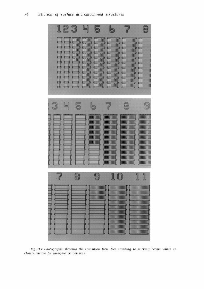
74 Stiction of surface micromachined structures
Fig. 3.7 Photographs showing the transition from free standing to sticking beams which isclearly visible by interference patterns.

Experimental 75
Interference contrast photographs of some test samples are shown in fig. 3.7.The residual strain of the polysilicon layer was measured by ring and buckledbeam structures and was typically found to be on the order of 10 ppm. For thedimensions of the samples in this paper and the measured residual strain, theconditions to neglect the influence of the residual strain are generally satisfied(see previous section).
The detachment length showed a large spread, especially the hydrophobicsamples dried from water. Often long beams are free standing while shorterbeams are sticking. Disturbances because of local surface asperities, dustparticles, etc. strongly reduce adhesion resulting in errors that lead to anincrease of the detachment length. In our experiments, the detachment lengthwas determined from the shortest sticking beams (i.e. giving the highestbonding strength). From the detachment length the surface energy can becalculated by eq. (3.11). The slope of the curves in fig. 3.7 is equal to [π4Ê/4γs]1/4.The corresponding surface energies for hydrophobic and hydrophilic samplesare listed in table 3.1.
Surface energy [J/m2]
liquid Hydrophobic Hydrophilic
H2O 0.05 ± 0.05 0.26 ± 0.1
IPA 0.10 ± 0.05 0.24 ± 0.1
Table 3.1 Surface energy of the different samples calculated from formula (11). A value of 166GPa was used for the plate modulus Ê. Residual strain is on the order of 10 ppm and can beneglected in our experiments.
The errors in the surface energies are worst case values and are mainlydetermined by the error in the slopes of the curve fits.
Because the roughness is important with respect to the adhesion properties,as discussed before, the surface roughness was measured by Atomic ForceMicroscopy. The root mean square values of the surface roughness of thebottom side of the microbridges varied from about 1 to 3 nm, depending on thethickness of the silicon oxide and polysilicon layer. The surface roughness ofthe silicon substrate after sacrificial layer etching was 0.2 nm. Measurementexamples are shown in fig. 3.8. These values are very small and imply that themeasured surface energies are only weakly influenced by the surface roughnessof the samples. Some samples were inspected by SEM to see if etch residueswere left behind after the etching and rinsing procedures, but only smooth and

76 Stiction of surface micromachined structures
100
200
300
400
500100
200
300
400
500
X 100 nm/divZ 2 nm/div
Microscope NSIII AFMScan size 546.0 nmSetpoint -1.5 VScan rate 2.4 HzNumber of samples 256Z range (Rp) 2.541 nmRMS (Rq) 0.2 nmMean roughness (Ra) 0.153 nmMax height (Rmax) 2.565 nm
100
200
300
400
500100
200
300
400
500
X 100 nm/divZ 5.125 nm/div
Microscope NSIII AFMScan size 546.0 nmSetpoint 0.0 VScan rate 4.7 HzNumber of samples 256Z range (Rp) 26.7 nmRMS (Rq) 3.1 nmMean roughness (Ra) 2.4 nmMax height (Rmax) 26.0 nm
Fig. 3.8 AFM scanning images of a silicon wafer and the bottom side of a polysilicon beam.Top figure: silicon wafer surface with RMS surface roughness of 0.2 nm. Bottom figure: bottomsurface of polysilicon beam with RMS surface roughness of 3.1 nm, the beam thickness is 1.67µm and silicondioxide thickness before release was 1.69 µm .

Experimental 77
clean surfaces were observed. Fig. 3.9 shows a SEM photograph of thedisappearing gap spacing between a sticking beam and the substrate.
Fig. 3.9 SEM Photograph of the disappearing gap spacing between a sticking beam and thesubstrate.
3.5 DISCUSSION
From fig. 3.5 it can be seen that the measured pull-in length shows a linearfit with the parameter [d2h3]1/4 as predicted by the theory. However, the slope ofthe curve is 41 µm-1/4, which is lower than the theoretical value of 79 µm-1/4,calculated from eq. (3.8) by using a plate modulus Ê of 166 GPa, a surfacetension γ for IPA of 21.7 mN/m [3.20] and zero degrees contact angles θ1 and θ2.The influence of the step-up boundary of the fabricated microbeams or otherassumptions for the deflection profile have been considered and only lead tosmall variations in the pull-in length and are thus unlikely to cause thediscrepancy. The difference might be due to the non-equilibrium situation thatexists during drying. The value used for the surface tension is only valid forIPA at thermodynamical equilibrium. During drying however, the liquid is notin equilibrium. Dynamic effects such as spreading may lead to in an increase ofthe capillary forces. In case of spreading, the difference can be enormous, and isabout 60 mN/m for organic liquids on oxides and 300 mN/m for water onmetallic oxides [3.21]. In our situation the increase would be 270 mN/m asdetermined from the pull-in measurements.

78 Stiction of Surface Micromachined Structures
The measured surface energies of sticking beams (table 3.1) can be comparedwith theoretically calculated values to determine which adhesion mechanismsare present. After the rinsing and drying procedures, as described above, noresidues have been observed by microscopic- or SEM inspection indicating thatadhesion by solid bridging is not present. From table 3.1 one can see that therinsing liquids which have been used hardly effect the adhesion energy andthat it is mainly determined by the surface properties (i.e. hydrophobic orhydrophilic) of the materials which have been used. Although meniscus forcesplay an important role in the initiation of the physical contact between thebeam and the substrate, the measured bonding energies are too small to beassociated with meniscus forces from a thin liquid film, remaining after dryingor initiated by microcapillary effects. Chemical bonding is also precluded forthe same reason. As already discussed, electrostatic forces are unlikely to exceedvan der Waals forces at small separations and are disregarded as a possiblecause for stiction. This leaves van der Waals forces and hydrogen bonding asthe possible causes for stiction.
The measured surface energies indicate that van der Waals forces areresponsible for the hydrophobic bonded surfaces and hydrogen bridging is anadditional bond mechanism for the hydrophilic bonded surfaces. The valuesfor the surface energy show a good correlation with hydrophobic andhydrophilic wafer bonding experiments [3.15]. In this case energies are found of0.04 to 0.1 J/m2 for hydrophobic wafers and 0.14 to 0.2 J/m2 for hydrophilicwafers bonded at room temperature.
In summary, stiction is accomplished in a two step process. First a temporaryphysical contact between surface micromachined structures and the substrate isinduced by dynamic capillary forces during the drying of the rinse liquid. Afterthis, permanent attachment is caused by van der Waals forces and hydrogenbridges which are induced by the small separation distance during this contact.
The maximum free standing length, the detachment length, is a function ofthe adhesion energy of the beam to the substrate surface and the mechanicalstiffness of the structures. The maximum free standing length can easily beincreased by increasing the beam thickness and the sacrificial layer thicknessand using larger tensile residual strains.
Stiction can be prevented or reduced in several ways which has already beendiscussed in the previous chapter. The methods are based upon the preventionof physical contact between the structures and the substrate during thefabrication process and on the reduction of the adhesional forces.

Conclusions 79
3.6 CONCLUSIONS
It has been shown that during the drying process, attractive capillary forcesare responsible for bringing micromechanical structures into contact with thesubstrate. A model for the surface tension forces during drying has beendeveloped and applied to doubly clamped beams. For these beams a pull-inlength exists beyond which the beams are forced into contact with theunderlying substrate. Measurements of the pull-in length are in qualitativeagreement with the theory. The measured values of the pull-in length aresomewhat lower than predicted by the theory. This is probably due todynamical effects during the drying process.
After complete drying, structures remain stuck to the substrate. Themeasured adhesion energy of the resultant bond has been determined usingthe detachment length of the beams after complete drying. The resultingbonding strength's were independent of the used rinsing liquids, water andisopropanol. The adhesion energy ranged from 0.05 to 0.10 J/m2 forhydrophobic silicon surfaces and 0.24 to 0.26 J/m2 for hydrophilic siliconsurfaces. These energies indicate that van der Waals forces are responsible forthe hydrophobic surfaces and hydrogen bridging is the dominant bondmechanism in case of the hydrophilic surfaces. These results are in agreementwith wafer bonding experiments.
REFERENCES
[3.1] H. Guckel, J.J. Sniegowski and T.R. Christenson, Advances in processing techniques forsilicon micromechanical devices with smooth surfaces, Proc. IEEE Micro ElectroMechanical Systems, Salt Lake City, Utah, U.S.A., June 6-9 1989, pp. 71-75.
[3.2] R.L. Alley, G.J. Cuan, R.T. Howe and K. Komvopoulos, The effect of release-etchprocessing on surface microstructure stiction, Proc. IEEE Solid-State Sensors and ActuatorsWorkshop, Hilton Head Island, SC, U.S.A. June 22-25, 1992, pp. 202-207.
[3.3] C. Linder, E. Zimmerman and N.F. de Rooy, Capacitive polysilicon resonator with MOSdetection circuit, Sensors and Actuators A, 25-27 (1991), 591-595.
[3.4] P.R. Scheeper, J.A. Voorthuyzen, W. Olthuis and P. Bergveld, Investigation of attractiveforces between PECVD silicon nitride microstructures and an oxidized silicon substrate,Sensors and Actuators A, 30 (1992) 231-239.
[3.5] C.H. Mastrangelo and C.H. Hsu, A simple experimental technique for the measurement ofthe work of adhesion of microstructures, Proc. IEEE Solid-State Sensors and ActuatorsWorkshop, Hilton Head Island, SC, U.S.A. June 22-25, 1992, pp. 208-212.
[3.6] W.C. Tang, T.C.H. Nguyen and R.T. Howe, Laterally driven polysilicon resonantmicrostructures, Proc. IEEE Micro Electro Mechanical Systems, Salt Lake City, Utah,U.S.A., Feb. 20-22,1989, pp. 53-59.
[3.7] H. A. C. Tilmans, Micro-mechanical sensors using encapsulated built-in resonant straingauges, Ph.D. thesis, University of Twente, January 1993, ch. 4.
[3.8] H. Krupp, Adv. Coll. Interf. Sci., 1 (1967), pp. 111-239.[3.9] J. Isrealachvilli, Intermolecular and Surface Forces, Academic Press, 2nd ed., 1991.

80 Stiction of surface micromachined structures
[3.10] J.Isrealachvilli, P. McGuiggan and R. Horn, Basic physics of interactions between surfacesin dry, humid and aqueous environments, Proc. The Electrochem. Soc. First Int. Symp. onSemiconductor Wafer Bonding, Phoenix, AZ, U.S.A., October 13-18, 1991, pp. 33-47.
[3.11] A.D. Zimon, Adhesion of dust and powders, 2nd ed., Consultants Bureau, New York, 1979.[3.12] R.A. Bowling, An analysis of particle adhesion on semiconductor surfaces, J. Electrochem.
Soc., Vol. 132, No. 9 (1985), pp. 2208-2214.[3.13] D. Gräf, M. Grundner and R. Schultz, The reaction of water with hydrofluoric acid
treated silicon (111) and (100) surfaces, J. Vac. Sci. Technol. A 7 (3), May/Jun 1989, pp.808-813.
[3.14] M. Grundner, D. Gräf, P.O. Hahn and A. Schnegg, Wet chemical treatment of Si Surfaces:chemical composition and morphology, Solid State Technology, Feb. 1991, pp. 69-75.
[3.15] Y. Bäcklund, K. Herrmansson and L. Smith, Bond strength measurements related to siliconsurface hydrophilicity, Proc. The Electrochem. Soc. First Int. Symp. on SemiconductorWafer Bonding, Phoenix, AZ, U.S.A., October 13-18, 1991, pp. 82-87
[3.16] R.K. Iler, The chemistry of silica, Wiley, New York, 1979, p. 177.[3.17] A Torii, M. Sasaki, K. Hane and S. Okuma, Adhesive force of the microstructures
measured by the atomic force microscope, Proc. IEEE Micro Electro Mechanical Systems,Fort Lauderdale, Florida, U.S.A., Feb. 7-10,1993, pp. 111-116.
[3.18] J.A. Greenwood and J.B.P. Williamson, Contact of nominally flat surfaces, Proc. R. Soc.Lond. A 295 (1966), pp. 300-319.
[3.19] K.N.G. Fuller and D. Tabor, The effect of surface roughness on the adhesion of elasticsolids, Proc. r. Soc. Lond., A 345 (1975), pp. 327-342.
[3.20] Handbook of chemistry and physics, 66 th ed., CRC press, 1985-1986[3.21] P.G. de Gennes, Wetting: statics and dynamics, Rev. Mod. Phys., Vol. 57, No. 3, Part 1,
July 1985, pp. 827-863.

8 1
Chapter Four
ANISOTROPIC REACTIVE ION ETCHING OFSILICON USING SF6/ O2/ CHF3 GAS MIXTURES*
Reactive ion etching of silicon, using SF6/O2/CHF3, plasmas in an RF parallel platesystem has been studied. Etching behaviour was found to be a function of loading, thecathode material and the mask material. Good results with respect to reproducability anduniformity have been obtained by using silicon as the cathode material and silicondioxide as the masking material for mask designs where most of the surface is etched.Etch rate, selectivity, anisotropy and self-bias voltage have been examined as a functionof SF6 flow, O2 flow, CHF3 flow, pressure and the RF power, using response surfacemethodology, in order to optimise anisotropic etching conditions. The effect of thevariables on the measured responses is discussed. The anisotropic etch mechanism isbased on ion-enhanced inhibitor etching. SF6 provides the reactive neutral etchingspecies, O2 supplies the inhibitor film forming species and SF6 and CHF3 generate ionspecies that suppress the formation of the inhibitor film at horizontal surfaces.Anisotropic etching of high aspect ratio structures with smooth etch surfaces has beenachieved. The technique is applied to the fabrication of three dimensionalmicromechanical structures.
4.0 INTRODUCTION
Dry anisotropic etching of silicon is an important technology for thefabrication of micromechanical devices. Dry etch characteristics are notconstrained by crystal planes as in the case of wet anisotropic etching forexample by KOH solutions. This has the advantage that not only singlecrystalline-silicon but also poly-crystalline silicon and amorphous-silicon canbe used for the fabrication of three-dimensional micromechanical structures.Dry etching techniques can be utilized to etch arbitrarily shaped mask designs.This is especially usefull for the fabrication of electrostatically drivenmicroactuators that often exhibit complex shapes and require small gap sizeswith high aspect ratio's.
Dry anisotropic etching of silicon has been achieved with Cl and Brcontaining gas mixtures such as SF6-CBrF3 [4.1], SF6-C2Cl3F3 [4.2] and SF6-C2ClF5 [4.3, 4.4]. Etching of silicon with SF6 at very low temperatures [4.5] or at
* published in J. Electrochem. Soc., Vol. 142, No. 6, June 1995, pp. 2020-2028.

82 Anisotropic reactive ion etching of silicon
very low pressures [4.6] can also be used to produce anisotropic etch profiles.Furthermore SF6/O2 gas mixtures [4.7-4.14] were found to anisotropically etchsilicon. The last technique has the advantage of being a fluorine based etchchemistry that can be used in common reactive ion etch systems. Generally,however, rough etch surfaces are produced that make the process less useful.
In this study the objective was to optimise the anisotropic etching of siliconby SF6-O2 plasmas and produce smooth etch surfaces by response surfacemethodology, using the etch system described below. This was accomplished bythe addition of CHF3 to the SF6/O2 plasma. The process is applied in thefabrication of micromechanical structures with high aspect ratio's.
4.1 EXPERIMENTAL
4.1.1 Equipment
Etching experiments were performed in an Electrotech, Plasmafab 310-340twin deposition/etch system. The RIE part consists of a parallel-plate systemwith a RF generator operating at 13.56 MHz and an automatic RF matchingnetwork. The pumping system consists of a turbo-pump in series with a rotary-pump. The spacing between the electrodes is fixed at 8.0 cm. The chamber wallsconsist of aluminium and the powered electrode has a diameter of 19 cm and iscovered with a titaniumdioxide coated, aluminium (styros) plate. Thetemperature of the lower electrode can be controlled from 10 to 60 ˚C, bybackside heating or cooling, using a temperature controlled oil-bath system.The flow rates of the gases were maintained with standard mass flowcontrollers. The pressure during processing is monitored with a capacitivemanometer and controlled automatically with a throttle valve.
4.1.2 Initial experiments
Loading:
Initial experiments showed that the etch behaviour of silicon in SF6/O2 gasmixtures is loading dependent with regard to macroloading (i.e. the amount ofwafers) and with regard to microloading (i.e. with regard to the pattern densityon the wafers). This effect has been investigated by several researchers [15-18].For our purpose we are interested in positive mask pattern designs that areequally distributed over the wafer, and where most of the wafer surface will beetched. The loading was kept constant at one 3" wafer per run in ourexperiments.

Experimental 83
Cathode material:
The etching behaviour is also depending on the cathode material [4.15].Three cathode materials; styros, graphite and silicon have been examined. Thegraphite and silicon electrode cover the styros electrode that is normallypresent in the reactor. Styros is a non-consumable material in contrast tographite and silicon that are etched in fluorine based plasmas. With the styroscathode, the etch rate at the wafer edge was twice as high compared to the etchrate at the center of the wafer. This non-uniformity is a result of gradients inlocal reactant concentrations and is controlled by the relative etch rates of thewafer vs. the cathode material [4.15]. The uniformity in case of the graphitecathode was measured to be about 20 percent. The use of the consumablesilicon cathode resulted in a uniformity of a few percent across the wafer. Inthis case the silicon etching rate as well as the selectivity to silicon dioxide werefound to be lower than in case of the other cathode materials. Because of thegood uniformity, the silicon cathode was used for further experiments.
Mask material:
During initial experiments, it was observed that etching is also affected by themask material. It has been suggested that the mask material may act as acatalyst for SF6 to generate fluorine [4.19, 4.20], thereby affecting the processconditions. For this reason a non catalytic mask material is preferred. In ourexperiments silicon dioxide has been used as the etch mask material.
CHF3 addition:
Anisotropic etching with SF6/O2 plasmas normally produces rough etchsurfaces. The silicon etch surfaces sometimes showed a black color as a result oflarge surface roughness (black silicon). This phenomenon has also beenreported by other investigators [4.7, 4.9, 4.11]. It was found that the addition ofCHF3 to the SF6/O2 plasma produced smooth etch surfaces. Therefore this gasmixture has been used in our experiments.
4.1.3 Sample preparation
In all of the experiments, the samples prepared were 3" diam., <100>oriented, p-type (5-10 Ωcm) silicon wafers. A 3000 Å thick SiO2 layer was grownby wet oxidation at 1000 ˚C. This layer was patterned by lithography and RIEusing CHF3 gas with a flow of 10 sccm, a process pressure of 20 mTorr, and anRF power of 50 Watt. The temperature of the oil bath, that controls the

84 Anisotropic reactive ion etching of silicon
temperature of the lower electrode, was set at 25 ˚C. After the etching of theSiO2 layer the resist was stripped by oxygen ashing. Before the etchingexperiments the etching chamber was manually cleaned with ethanol and byan oxygen plasma cleaning step. Before each experiment the wafer was givenan HF-dip (HF:H2O = 1:100) for one minute to remove the native oxide layer.The gas flows and process pressure were allowed to stabilize for five minutesbefore etching was performed.
4.1.4 Experimental design
The characteristics of the etch process are explored using a statisticalexperimental design [4.21, 4.22] and are modelled empirically by responsesurface methodology. In general a design should be chosen that will support afull quadratic model, which includes linear terms, two factor interactions, andquadratic terms for curvature. The general form of the full quadratic model is:
Y = b0 + biXi∑
i=1
f+ biiXi
2∑i=1
f+ bijXiXj∑
j=2
f∑
i=1
f-1(4.1)
where the X i represent the independant input variables (i.e., processparameters), the bi are the coefficients for the linear terms, the bii are thecoefficients for the quadratic terms, and the bij are the coefficients for the crossterms. A more elucidated discussion of surface response methodology is givenin Appendix A.
For the optimisation of the RIE process the SF6 flow, the O2 flow, the CHF3
flow, the pressure and the RF power have been chosen as the process variables.These process variables have been varied within the limits of our etchingsystem. The temperature of the oil-bath that controls the cathode temperaturewas set at 25 ˚C. No special clamping or temperature control of the wafer wasused. The loading was constant at one 3" wafer. A central composite rotatablesecond order design was used for the experiment. The monitored responses arethe self-bias voltage, the silicon etch rate, the uniformity, the etch surfaceroughness, the selectivity and the anisotropy. The normalized experimentaldesign information is given in table 4.1 whereas table 4.2 shows the actualparameter settings. The order of performing the experimental trials wasrandomized to minimize the effect of any systematic error.

Experimental 85
R u n
#
SF6 O2 CHF3 p P
1 - 1 - 1 - 1 - 1 +1
2 +1 - 1 - 1 - 1 - 1
3 - 1 +1 - 1 - 1 - 1
4 +1 +1 - 1 - 1 +1
5 - 1 - 1 +1 - 1 - 1
6 +1 - 1 +1 - 1 +1
7 - 1 +1 +1 - 1 +1
8 +1 +1 +1 - 1 - 1
9 - 1 - 1 - 1 +1 - 1
10 +1 - 1 - 1 +1 +1
11 - 1 +1 - 1 +1 +1
12 +1 +1 - 1 +1 - 1
13 - 1 - 1 +1 +1 +1
14 +1 - 1 +1 +1 - 1
15 - 1 +1 +1 +1 - 1
16 +1 +1 +1 +1 +1
17 - 2 0 0 0 0
18 +2 0 0 0 0
19 0 - 2 0 0 0
20 0 +2 0 0 0
21 0 0 - 2 0 0
22 0 0 +2 0 0
23 0 0 0 - 2 0
24 0 0 0 +2 0
25 0 0 0 0 - 2
26 0 0 0 0 +2
27 0 0 0 0 0
28 0 0 0 0 0
29 0 0 0 0 0
30 0 0 0 0 0
31 0 0 0 0 0
32 0 0 0 0 0
Table 4.1 Nonrandomized experimental design for five normalized parameters.

86 Anisotropic Etching of Silicon
Variable -2 -1 0 1 2
SF6 flow [sccm] 10 20 30 40 50
O2 flow [sccm] 2 6 10 14 18
CHF3 flow
[sccm]
2 7 12 17 22
pressure
[mTorr]
20 60 100 140 180
power [Watt] 20 60 100 140 180
Table 4.2 Variable settings used for the experimental design.
4.1.5 Data aquisition
The thickness of the SiO2 layer was measured by ellipsometry before andafter the etching process to determine the etch rate of this layer. A correctionwas made for the HF-dip which was measured to remove about 50 Å of theoxide layer before the experiments. After etching, the etch depth of the siliconwas measured with a Dektak surface profiler. The result was corrected for theremaining thickness of the oxide layer. The etch depth was measured at thecenter and at four points at 1 cm from the edge of the wafer to obtain anindication of the uniformity of the etch process. The selectivity was foundfrom the ratio of the silicon etch depth and the difference in the SiO2 thicknessbefore and after the experiment. To determine the anisotropy, the sampleswere broken and their cross-section was examined by SEM. Several differentetch profiles have been obtained. Depending on the process conditions notonly mask undercut, but outward sloped profiles have also been observed. Theanisotropy is defined by:
A = 1 -
VH
(4.2)
where H is the etch depth and V is the maximal undercut of the mask or, incase of outward sloped profiles, the lateral extension of the sidewall as shownin fig. 4.1. This definition of the anisotropy does not give information whetherthe anisotropy is due to mask undercut or to outward sloped profiles. Howeverthe expression in equation (4.2) is generally used and therefore preferred for acomparison with results from other workers. A value of 1 represents a perfectvertical sidewall with no mask undercut.

Experimental 87
H
V
H
V
H
V
Fig. 4.1 Definition of anisotropy.
The roughness of the etch surface was only regarded qualitatively by means ofthe visual reflectivity of the silicon surface after etching, and by examining theetch surface of the cross-sectional SEM photographs.
In our experiments post structures and lines and spacings of 1,2 and 5 µmhave been used to determine the etch rate and anisotropy for etch depth ofabout 2 µm. At these dimensions no feature size dependent etch effects havebeen noticed. However effects like RIE lag and charging, may affect etch resultsat larger etch depth's [4.17].
4.2 RESULTS AND DISCUSSION
The responses of the factorial design are shown in table 4.3. The independentinput variables in formula (4.1) have been normalized as follows:
Xi = φi – φi / σ i (4.3)
Where X i is the normalized value for the variable setting φi, φi is thecenterpoint value of that variable and σi is the step of the variable that hasbeen used in the factorial design (see table 4.2).
The responses of the self-bias voltage, the silicon etch rate, the selectivity,and the anisotropy are fitted by the quadratic model (formula 4.1). Theregression coefficients bi,bii,bij and the fit coefficient R2 for the quadratic modelare shown in table 4.4. Graphical representation of the responses and SEMphotographs of sample cross sections are shown in fig. 4.2-4.8. In the graphs allparameters except for the specific parameters being varied are fixed at thecenter point of the design.

88 Anisotropic reactive ion etching of silicon
Run
#
Bias
Voltage [V]
Rate
[µm/min]
Selec-
tivity
Aniso-
tropy
Unifor-
mity [%]
Sur-
face
1 477 0.430 5.9 0.590 1.0 s m o o t h
2 47 0.320 13 0.690 2.4 s m o o t h
3 232 0.200 4.7 0.940* 2.8 r o u g h
4 339 0.670 10 0.880 3.9 s m o o t h
5 224 0.200 5.2 0.810 2.0 s m o o t h
6 343 0.460 5.1 0.620 3.9 s m o o t h
7 517 0.420 6.3 0.980 5.8 s m o o t h
8 72 0.310 10 0.960 1.2 s m o o t h
9 31 0.120 14 0.886* 1.9 r o u g h
10 50 0.550 11 0.560 4.2 s m o o t h
11 224 0.400 6.0 0.810* 1.3 r o u g h
12 27 0.0550 13 0.700 2.7 s m o o t h
13 154 0.350 5.6 0.640 8.1 s m o o t h
14 28 0.130 30 0.460 1.9 s m o o t h
15 42 0.190 12 0.886* 2.7 r o u g h
16 64 0.580 10 0.940 4.9 s m o o t h
17 366 0.240 5.1 0.881* 3.6 r o u g h
18 47 0.490 12 0.690 2.3 s m o o t h
19 62 0.360 6.4 0.940 7.6 s m o o t h
20 108 0.350 11 0.970* 1.2 r o u g h
21 58 0.360 9.3 0.938* 2.2 r o u g h
22 135 0.360 7.7 0.830 5.2 s m o o t h
23 448 0.360 5.9 0.730 3.8 s m o o t h
24 35 0.270 20 0.844* 3.7 r o u g h
25 23 0.00680 6.8 0.900 3.3 s m o o t h
26 356 0.600 7.2 0.660 3.5 s m o o t h
27 88 0.450 9.7 0.970 5.5 s m o o t h
28 85 0.440 10 0.940 6.3 s m o o t h
29 86 0.430 9.2 0.950 3.8 s m o o t h
30 84 0.450 10 0.970 2.3 s m o o t h
31 87 0.430 8.9 0.970 3.7 s m o o t h
32 85 0.430 9.4 0.960 3.9 s m o o t h
Table 4.3 Responses of the factorial design. In case of outward sloped etch profiles theanisotropy is marked by an asterisk.

Results and discussion 89
Coef. Rate Selec-
tivity
Aniso-
tropy
DCB
b0 0.434 9.34 0.969 87
b1 0.052 2.34 -0.066 -65
b2 0.010 -0.36 0.079 11
b3 0.004 -0.14 0.004 7
b4 -0.043 2.90 0.008 -102
b5 0.147 -1.72 -0.043 89
b11 -0.014 -0.05 -0.040 29
b22 -0.017 -0.01 -0.013 - 1
b33 -0.016 -0.06 -0.023 2
b44 -0.027 1.05 -0.035 38
b55 -0.030 -0.44 -0.056 25
b12 0.003 -0.90 0.029 - 6
b13 -0.008 0.60 0.004 4
b14 -0.016 0.65 -0.039 23
b15 0.035 -1.11 0.058 -14
b23 0.028 0.16 0.054 -17
b24 -0.007 -1.34 -0.016 2
b25 0.018 1.70 0.035 5
b34 0.022 1.29 -0.019 7
b35 -0.023 -1.15 0.028 - 3
b45 0.027 -1.93 0.008 -46
s 0.01 0.5 0.01 1.5
R2 0.99 0.90 0.95 0.99
Table 4.4 Fitted coefficients of the quadratic model for the reponses. The s value at thebottom of each column is an estimate of the standard deviation for that response. The R2 indexindicates the agreement between model and data. A value of 1.00 denotes an ideal fit.

90 Anisotropic reactive ion etching of silicon
4.2.1 Etch Rate
In fig. 2 the effect of the SF6 and O2 flow, and the effect of the pressure andRF power, on the etch rate of silicon are shown. The silicon etch rate shows aquadratic dependency on the SF6 flow, the O2 flow, the process pressure andthe RF power. The rate is independent of the CHF3 flow. The accuracy of themodel is indicated by the squared multiple R2 which is 0.99 and represents agood fit.
To understand the etch behaviour, some background of the etch mechanismis needed. It is well known that plasma etching of silicon with fluorinatedcompounds is primarily due to free fluorine [4.23]. The dissociation of SF6 isassumed to involve electron impact dissociation reactions of the form:
e + SFxg→ SFx – 1g
+ Fg + e (x = 3–6) (4.4)
The etching of silicon occurs by a reaction with F atoms. The overallstochiometry of etching by atomic F is [4.24]:
Si + 4 F → SiF4 (4.5)
The etch rate RSi can be written as:
RSi = k βSi nF (4.6)
where k is a constant, βSi is the reaction probability of fluorine at the surfaceand nF is the density of fluorine atoms. Higher SF6 flows will increase thefluorine concentration in the gas mixture, resulting in higher etch rates. Athigh flows, the fluorine concentration can decrease due to higher convectivelosses (see section on total flow rate) and the etch rate will start to decrease.
The influence of oxygen addition to SF6 plasmas has been investigated byseveral authors [4.11-4.14, 4.25-4.27]. With an SF6-O2 mixture in the absence ofsilicon, the final reaction products are F2, SOF4, and SO2F2. When Si is etched,SiF4 is the only stable silicon-containing etch product and SOF2 is formed inoxygen-poor mixtures. It was found that oxygen additions drastically increasethe conversion of the feed gas, evidently by reacting with fluorosulfur radicalsand thus preventing their recombination with fluorine to reform SF6 [4.12].
SFx + F→ SFx – 1 (x = 5–1) (4.7)

Results and discussion 91
10
2030
40
50
5
10
15
0.2
0.3
0.4
Etch Rate[µm/min]
SF6 flow[sccm]
O2 flow[sccm]
5050
50
100
150
100
1500.2
0.4
0.6
50
100
150
100
1500
0.6
Etch Rate[µm/min]
Pressure[mTorr]
Power[Watt]
Fig. 4.2 Surface plots showing the silicon etch rate as a function of the SF6 and O2flow, and as a function of the process pressure and the RF power. All parameters exceptfor the specific parameters being varied are fixed at the center point of the design.

92 Anisotropic reactive ion etching of silicon
This leads to a net increase of F atoms. As the feed is made more O2 rich,SO2F2 increases with respect to SOF4 while the F-atom concentration firstincreases, reaches a maximum, and then decreases. These results closelyparallel analogous trends in the carbon-based CF4-O2 system [4.24].
When silicon is exposed to the discharge, a significant change in the productcomposition is observed. SOF2 is formed in oxygen-poor mixtures, SiF4
appears, and the concentration of molecular fluorine is depressed [4.13]. As thequantity of oxygen is increased, the etch rate goes through a maximum andsubsequently decreases.
In the presence of oxygen, oxygen species compete with F for active surfacesites. This has been explained by a quantitative model which takes oxygenadsorption into account to relate the etch rate to the fluorine concentration forsilicon and SiO2 etching in CF4-O2 plasmas [4.24]. The decrease of the reactionprobability was found to be:
β ' =β
1 + C nO / nF(4.8)
where β' is the reaction probability in the presence of oxygen, nO is the densityof oxygen atoms and C is a constant. Maneschijn [4.28] showed that this modelalso represents the data for SF6-O2 gas mixtures quite well.
Thus at higher O2 flows the etch rate will be depressed as a result of thecompetition of oxygen atoms with fluorine atoms for chemisorption on thesilicon surface.
As was pointed out by Tzeng [4.11], increasing the RF power leads to asignificant increase of the atomic fluorine concentration while the oxygenconcentration increases only slightly. This explains the increased siliconetching rate with increasing RF power.
At low RF power the etch rate decreases with increasing pressure, while athigh RF power the etch rate first increases, reaches a maximum and finallydecreases with increasing pressure. These results agree with the experiments ofKopalidis [4.12]. By measuring the effect of pressure on the dischargecomposition of SF6-O2 plasmas they found that the main effect of increasingpressure is to enhance the oxyfluoride production rates, thus reducing therecombination reactions. In accordance with our results, the self-bias wasfound to decrease strongly with increasing pressure. Assuming that ionbombardment contributes significantly to the overall etching rate (thesynergistic effect of ion bombardment and chemical etching), the decrease in

Results and discussion 93
20
30
40
50
5
10
15
0
5
10
1020
30
40
50
5
10
15
0
5
10
15
Selectivity
SF6 flow[sccm]
O2 flow[sccm]
5050
50
100
150
100
150
0
10
20
50
100
150
100
150
0
10Selectivity
Pressure[mTorr]
RF Power[Watt]
Fig. 4.3 Surface plots showing the selectivity as a function of the SF6 and the O2 flow, and asa function of the process pressure and the RF power.

94 Anisotropic reactive ion etching of silicon
the etch rate with increasing pressure can be explained by the decrease in ionbombardment at higher pressures.
At high RF power the initial increase of the etch rate with increasingpressure may be the result of an increasing F concentration and ion density thatleads to a larger ion flux towards the substrate.
4.2.2 Selectivity
The selectivity linearly increases with the SF6 flow and linearly decreaseswith the O2 flow and the RF power, and only sligthly decreases with increasingCHF3 flow. It shows a quadratic dependancy on the pressure. Surface plotsshowing the selectivity as a function of the SF6 and the O2 flow, and as afunction of the process pressure and the RF power are shown in fig. 4.3. The R2
index indicates a good model fit.The selectivity is the quotient of the etch rates of silicon and silicon dioxide.
The effect of the process parameters on the silicon etch rate have beendiscussed. The etch rate of SiO2 is to a large extent due to direct etching byreactive ions. It was reported that the etch rate of SiO2 in a CHF3-O2 plasma wasfound to follow the ion density and to be fairly independant of the plasmachemistry under most experimental conditions [4.29]. Ion bombardmentincreases with increasing RF power and with decreasing pressure. This resultsin a decrease of the SiO2 etch rate with increasing RF power and an increase ofthe SiO2 etch rate with increasing pressure. Assuming that the SiO2 etch rate inthis process is also fairly independent of the plasma chemistry, this leads to anincrease of the selectivity with increasing SF6 flow and increasing pressure(more chemical etching) and a decrease of the selectivity with increasing RFpower and O2 flow and CHF3 flow (more physical etching).
4.2.3 Anisotropy
Responses of the anisotropy are shown in fig. 4.4. The anisotropy shows alinear increase with the O2 flow. It is quadratically dependent on the processpressure, the RF power and the SF6 flow. Furthermore the anisotropy shows aweak quadratic dependency on the CHF3 flow. Again the fit between the dataand the model is good.
Fig. 4.5 shows a selection of the sidewall profiles, which have been obtainedin our experiments. These photographs clearly demonstrate that it is difficultto obtain a straightforward definition of the anisotropy. Depending on processconditions profiles may vary from isotropic to outward sloped profiles.

Results and discussion 95
5
10
2030
40
50
10
15
0.4
0.6
0.8
1
SF6 Flow[sccm]
O2 Flow[sccm]
Anisotropy
50
100
150
50
100
1500.6
0.8
Pressure[mTorr]
RF Power[Watt]
Anisotropy
Fig. 4.4 Surface plots showing the anisotropy as a function of the SF6 and O2 flow,and as a function of the process pressure and the RF power.

96 Anisotropic reactive ion etching of silicon
a) b)
c) d)
Fig. 4.5 Sidewall profiles obtained under different process conditions. The parameter settingsare shown in tabel 1 and 2 for: a) fact. nr. 24, b) fact. nr. 27, c) fact. nr. 13 and d) fact. nr. 6.

Results and discussion 97
Note that at high pressures and high O2 flows the value of the anisotropy, asdefined before, may be lower because of outward sloped etch profiles.
Auger Electron Spectroscopy (AES) data, taken within 15 minutes after theetch process, from the sidewall and bottom etch surface of a center point run isshown in fig. 4.6. Approximately equal amounts of sulfur and carbon weredetected on both surfaces. Sulfur is most likely a product of the SF6 gas andcarbon may result from the CHF3 gas or from organic contamination. Thepresence of fluorine was not observed. However, this may be due to electronstimulated desorption of fluorine atoms as a result of the measurement.Oxygen is present on both surfaces. The amount of oxygen on the sidewallsurface is much higher than the amount of oxygen on the bottom surface. Thisclearly indicates a sidewall passivation effect by oxygen species, as proposed byZhang [4.14]. On the horizontal silicon surfaces, adsorption of oxygen residuecan be readily attacked through the physical bombardment of active ion specieslike SFx+ and CFx+. While on the the vertical Si surfaces (sidewalls), theremoval of sidewall material is not significant because of the less directionalkinetic energy in this orientation. These results are in agreement with otherinvestigations [4.7, 4.30, 4.31].
Surface and interfacial residue films formed on polycrystalline silicon andsilicon dioxide by reactive ion etching with SF6-10% O2 at 100 mTorr have beeninvestigated using x-ray photoemission spectroscopy [4.30]. Composition andchemistry at the surface were found to be variations of SiOxFy. The thicknessvaried from 7 to 13 Å with a decreasing etch rate. Silicon surfaces etched inC F 4- O 2 plasma have been characterised with the use of in situ x-rayphotoemission spectroscopy [4.31]. It was found that a SiOxFy layer onelemental silicon was formed under all conditions. For oxygen percentagesgreater than 5% in the feed gas, the oxygen content of the film and the filmthickness increased, whereas the fluorine content of the film decreased.
These observations may explain the increase of the anisotropy withincreasing O2 flow and the decrease of the anisotropy with increasing SF6 flowby affecting the formation of the sidewall passivation layer. At high O2 flowsand low SF6 flows, profiles are positively tapered (outward sloped) and theanisotropy shows an initial increase with the SF6 flow. In this region, theformation of the passivation layer is very pronounced and outward sloped etchprofiles are obtained that may be the result of an orientation dependant etchrate. Increasing the SF6 flow at high O2 flows, increases the F concentration,thereby reducing the formation of the passivation layer on outward slopedprofiles which leads to a more vertical etch profile that has a higher anisotropy.

98 Anisotropic reactive ion etching of silicon
Inte
nsit
y
Kinetic Energy [eV]
1000
500
0
-500
-1000
-1500
Si
SC
O
Si
500 1000 1500 20000
sidewall surfaceIn
tens
ity
Kinetic Energy [eV]
1000
500
0
-500
-1000
-1500 Si
SC
O
Si
500 1000 1500 20000
bottom surface
Fig. 4.6 AES data of the sidewall and bottom etch surface after etching of a centerpoint run.
Results and discussion 99
It has been found that increasing the pressure increases the atomic fluorineconcentration and decreases the ion bombardment [4.12]. Both effects lead to areduction of the anisotropy in agreement with our results at high pressures. Atlow pressures, however, the anisotropy increases with increasing pressureuntil it reaches a maximum. This may be explained by a low silicon surfacecoverage by oxygen atoms. The surface coverage is a function of the pressureand increases with increasing pressure. Apparently the oxygen concentration atlow pressures is too small to result in a surface coverage that is high enough toform a stable passivation layer.
The RF power gives an initial increase, reaches a maximum and then resultsin a decrease of the anisotropy with increasing RF power. Increasing the RFpower increases the F concentration as well as the ion bombardment on thehorizontal surface. At low RF power it seems that the effect of the increase inion bombardment is stronger than the effect of the increasing F concentration,giving a net increase in the anisotropy. At higher RF power the increase in theF concentration probably becomes dominant and reduces the formation of thepassivation layer. This leads to a decrease in the anisotropy with increasing RFpower.
Adding CHF3 to the SF6-O2 plasma may influence the O to F concentration.In CHF3-O2 plasmas the major reaction products are CFx species, CO, CO2 andCOF2 [4.31]. These reactions will lower the O atom concentration. Since theselectivity (i.e the SiO2 etch rate) is only sligthly affected by the CHF3 addition itis suggested that the formation of the passivation layer is suppressed by anadditional competition of oxygen with CFx species on the surface. This effect isassumed to be more pronounced at the horizontal surfaces because the etchmechanism of silicon oxide, by CFx species, is ion enhanced where ions are themain reactants in the etch reaction [4.29]. For high CHF3 flows the reduction ofthe O atom concentration and passivation layer formation eventually result inmore isotropic etching profiles (see fig. 4.8).
4.2.4 Total gas flow
It should be noted that the total gas flow in the experiments is not constantand changes, depending on the SF6, O2 and CHF3 gas flow settings, from aminimum value of 32 sccm to a maximum value of 72 sccm. As a result, theresidence time of the gases is not constant. Longer residence times will lead to ahigher conversion of the etch gases into lower molecular weigth products. Theetch rate dependency as a function of the total flow rate for SF6/O 2 gas

100 Anisotropic reactive ion etching of silicon
mixtures has been studied by Tandon, and Kopalidis [4.8, 4.32]. At lowpressures an increase in total flow rate is accompanied by an increase in thedissociation of SFx molecules and radicals. The etch rate is limited by thesupply of fluorine atoms while at high flow rate, the etch rate decreases due toconvective losses. At high pressure and low flow rate, etchant production is atits maximum and increasing flow rates causes the fluorine concentration todecrease due to higher convective losses (active species are pumped awaybefore they have an opportunity to react).
4.2.5 Uniformity
As shown in tabel 4.4 the uniformity does not show a large variation whenthe parameter settings are changed. Only a few points per wafer have been usedto determine the uniformity leading to a relatively large standard error. Theaverage uniformity of the etch rate is 3.5 percent with a standard deviation of1.4 percent. A small increase is observed for high SF6 flows and high pressures.The uniformity is mainly a function of loading and cathode material asdiscussed in the section on initial experiments.
4.2.6 Self-Bias Voltage
The bias voltage is quadratically dependent on the SF6 flow, the RF powerand the pressure. It increases linearly with the O2 flow and the CHF3 flow. Themodel fit of the experimental values is very good as indicated by the R2 indexwhich equals 0.99. The results are presented graphically in fig. 4.7.
SF6 is used as a gaseous insulator because of its electronegativity. Increasingthe SF6 flow makes the discharge more electronegative due to a lower ratio ofelectrons to positive ions and the self-bias voltage decreases.
The decrease of the DC bias voltage with pressure is a result of a decrease inthe electron energy as the pressure is increased [4.12]. The increase of the DCBias with increasing O2 flow and CHF3 flow, is a consequence of a shift of theelectron energy distribution to higher values [4.12].
4.2.7 Etch surface roughness
It was observed that the etch surface roughness showed a correlation to wafercleanliness. A cleaning step, followed by an HF-dip were sufficient to reducethe etch surface roughness in this case, indicating that etch residue fromprevious steps or native oxide could be responsible for this effect. In spite of

Results and discussion 101
1020
3040
50
5
10
15
0
100
200
300
SF6 Flow[sccm]
O2 Flow[sccm]
Self BiasVoltage [V]
0200400
600
800
50
100
15050
100
150
Pressure[mTorr]
Power[Watt]
Self BiasVoltage [V]
Fig. 4.7 Surface plots showing the bias voltage as a function of the SF6 and the O2flow, and as a function of the process pressure and the RF power.

102 Anisotropic reactive ion etching of silicon
a)
b)
c)
Fig. 4.8 SEM photograps showing the influence of the CHF3 addition with respect to thesurface roughness and etch profile. All parameter settings except for the CHF3 flow are set at thecenter point, a) 2 sccm CHF3; b) 12 sccm CHF3; c) 22 sccm CHF3.

Results and discussion 103
these precautions rough etch surfaces have been observed after the etchingprocess and were found to be a function of the etch parameters. This indicatesthat rough etch surfaces are also generated by the etching process itself. At highpressures and high O2 flows, in the anisotropic etching regime, the etch surfaceroughness increases. The addition of CHF3 to an SF6/O2 gas mixture improvesthe etch surface quality, as shown in figure 4.8. When no CHF3 is added, theetch surface roughness, in the anisotropic etch regime, is high as a result of"micrograss". The addition of CHF3 results in smooth surfaces, only slightlyaffecting the anisotropy. At high CHF3 flows, the anisotropy will be lost andmore isotropic etching is obtained.
It is suggested that surface roughness is the result of silicon oxide micromasking. It has been shown that during etching in SF6 plasmas, large amountsof Si particles are generated [4.33]. When oxygen is added to SF6 plasmas theseparticles may also contain silicon oxide. Redeposition of these particles on theetch surfaces results in micromasking leading to the development of surfaceroughness (micrograss) in case of anisotropic etching. Another possibility isthat the surface roughness results from variations in thickness of theoxyfluoride layer on the horizontal silicon surfaces.
The presence of CFx species in the plasma may supress the formation and/oroxidation of the particles that are generated by the plasma or reduce theirmasking effect and suppresses the formation of the passivation layer on thehorizontal surface by chemical and physical attack. Note that CFx species maynot only be produced by the etch gas but also by photoresist or reactorcomponents like a graphite cathode.
Mask
Si
SFx+, CFx+
F*O*
SiF4SOxFy
COxFySiO
xFy
Fig. 4.9 Schematic drawing of the SF6, O2, CHF3 etch process.
In summary it can be concluded that the anisotropic etch mechanism isbased upon an ion-enhanced inhibitor etching process. This mechanismrequires three ingredients: 1 reactive neutral species, 2 inhibitor film forming

104 Anisotropic reactive ion etching of silicon
species, and 3 vertical ion flux to the substrate to prevent growth or etch theinhibitor film at the horizontal surfaces. These mechanisms can be more orless controlled indepedently by the three etch gasses. SF6 produces the Fradicals for the chemical etching of the silicon. O2 creates the O radicals topassivate the silicon surface by silicon oxide species. CHF3 produces CFx ionsthat, in addition to SFx ions, suppress the formation of the passivation layer athorizontal surfaces. The etch process is schematically shown in fig. 4.9.
4.3 APPLICATIONS
The process parameters optimized for high anisotropy are very usefull forthe fabrication of deep trenches and micromechanical structures. Theoptimized process parameter settings result in an anisotropy of 0.98, an etchrate of 0.5 µm/min, a selectivity with SiO2 of 10 and a smooth etch surface. Notonly monocrystalline silicon but also LPCVD polysilicon and sputtered siliconfilms have been used to fabricate micromechanical structures. In fig. 4.10 and4.11 SEM photographs are shown that clearly demonstrate the usefullness ofthe RIE process for high aspect ratio structures. The selectivity of the silicondioxide mask limits the etch depth. This problem can be solved by using metaletch masks. For instance with a chromium etch mask very high selectivities(>500) have been obtained, whereas etch characteristics are only slightlyaffected. Applications of this etch process, with respect to deep trench etchingand other mask materials, has been presented elsewhere [4.34, 4.35].
4.4 CONCLUSIONS
Reactive ion etching using SF6, O2, CHF3 gas mixtures for the anisotropicetching of silicon has been investigated. The etching behaviour was found tobe affected by loading, the mask material and the cathode material.Reproducable and uniform results have been obtained by using a siliconcathode and a silicon dioxide mask. Surface response methodology was used tocharacterize etch rate, mask selectivity, bias voltage and anisotropy as afunction of the RF power, the process pressure, the SF6 flow, the O2 flow andthe CHF3 flow in order to optimise anisotropic etching conditions. The effect ofseveral variables on the measured responses has been discussed. The additionof CHF3 can be used to produce smooth etch surfaces in the anisotropic regimeand is usefull for a fine tuning of the anisotropy.

Conclusions 105
Fig. 4.10 SEM photograph showing 1, 2 and 5 µm lines and spacings etched to a depth ofplusminus 10 µm. For the 1 and 2 µm structures the effect of RIE lag is clearly visible.
Fig. 4.11 SEM photograph of a stator-rotor structure of an electrostatic micromotor. Diameterof the rotor is 100 µm, etch depth is 13 µm and the rotor-stator gap spacing is 2 µm.

106 Anisotropic reactive ion etching of silicon
AES measurements indicate that anisotropic etching results from sidewallpassivation by silicon oxide species. The anisotropic etch mechanism in SF6,O2, CHF3 plasmas is based on ion-enhanced inhibitor etching. SF6 provides thereactive neutral etching species, in the form of F atoms. O2 supplies theinhibitor film forming species that passivate the surface with a SiOxFy layer.SF6 and CHF3 generate ion species, SFx+ and CFx+ respectively, that suppressthe formation the inhibitor film at horizontal surfaces.
The fabrication of structures with aspect ratios of about 10 has beendemonstrated. The process is applied to deep trench etching and fabrication ofhigh aspect ratio structures used in micromachining.
REFERENCES
[4.1] A.M. Krings, K. Eden and H. Beneking, RIE etching of deep trenches in Si using CBrF3 andSF6 plasma, Microelectronic engineering, 6, 553-558 (1987).
[4.2] V.A. Yunkin, D. Fischer and E. Voges, Highly anisotropic selective reactive ion etchingof deep trenches in silicon, Microelectronic Engineering, 23, 373-376 (1994).
[4.3] C. Linder, T Tschan and N.F. de Rooy, Deep dry etching techniques as a new ICcompatible tool for silicon micromachining, Proc. of the 6th Int. Conf. on solid-stateSensors and Actuators (Transducers '91), June 24-27, 1991, San Fransisco, CA, U.S.A., pp.524-527.
[4.4] J.P. McVittie and C. Gonzalez, Anisotropic etching of Si using SF6:C2ClF5, ExtendedAnstracts, Fall meeting, Electrochem. Soc., Vol. 84-2, pp. 584-585.
[4.5] A.J. Watts and W.J. Varhue, Low temperature etching of silicon trenches with SF6 in anelectron cyclotron resonance reactor, J. Vac Sci Technol. A, 10, 1313-1317 (1992).
[4.6] C. Pomot, B. Mahi, B. Petit, Y. Arnal and J. Pelletier, Anisotropic etching of silicon usingan SF6/Ar microwave multipolar plasma, J. Vac. Sci. Technol. B, 4, 1-5 (1986).
[4.7] T. Syau, B. J. Baliga and R.W. Hamaker, Reactive ion etching of silicon trenches usingSF6/O2 gas mixtures, J. Electrochem. Soc., 138, 3076-3081 (1991).
[4.8] U.S. Tandon and B.P. Pant, The characteristics of reactive ion etching of polysilicon usingSF6/O2 and their interdependence, Vacuum, 42, 837-843 (1991).
[4.9] R. Pinto, K.V. Ramanathan and R.S. Babu, Reactive ion etching in SF6 gas mixtures, J.Electrochem. Soc., 134, 165-175 (1987).
[4.10] C.P. D'Ernic, K.K. Chan and J. Blum, Deep trench plasma etching of single crystal siliconusing SF6/O2 gas mixtures, J. Vac. Sci. Technol. B, 10, 1105-1110 (1983).
[4.11] Y. Tzeng and T.H. Lin, Dry etching of silicon materials in SF6 based plasmas, roles ofN2O and O2 gas additives. J. Electrochem. Soc., 134, 2304-2309 (1987).
[4.12] P. M. Kopalidis and J. Jorne, Langmuir probe measurements and characterization of siliconetching in SF6/O2 discharges. J. Electrochem. Soc., 139, 839-844 (1992).
[4.13] R. d'Agostino and D.L. Flamm, Plasma etching of Si and SiO2 in SF6-O2 mixtures, J.Appl. Phys., 52, 162-167 (1981).
[4.14] M. Zhang, J.Z. Li, I. Adesida and E.D. Wolf, Reactive ion etching for submicron structuresof refractory metal silicides and polycides, J. Vac. Sci. Technol. B, 1, 1037-1042 (1983).
[4.15] A.G. Nagy, Radial etch rate nonuniformity in reactive ion etching, J. Electrochem. Soc.,131, 1871-1875 (1984).
[4.16] C.J. Mogab, The loading effect in plasma etching, J. Electrochem. Soc., 124, 1262-1268(1977).
[4.17] R.A. Gotscho and C.W. Jurgensen, Microscopic uniformity in plasma etching, J. Vac. Sci.Technol. B, 10, 2133-2147 (1992).

References 107
[4.18] R.W. Light and H.B. Bell, Profile control of polysilicon lines with an SF6/O2 plasmaetch process, J. Electrochem. Soc., 130, 1567-1571 (1983).
[4.19] G.W. Grynkewich, T.H. Fedynyshyn and R.H. Dumas, The effect of aluminium masks onthe plasma etch rates of polysilicon and silicon nitride, J. Vac. Sci. Technol. B8 , 5-9(1990).
[4.20] T.H. Fedynyshyn, G.W. Grynkewich and Tso-Ping Ma, The effect of aluminium vs.photoresist masking on the etch rates of silicon and silicon dioxide in fluorine containingplasmas, J. Electrochem. Soc., 134, 2580-2585 (1987).
[4.21] W.G Cochran and G.M. Cox, Experimental designs, 2 nd ed., John Wiley & Sons, Inc. 1964.[4.22] G.E.P. Box, W.G. Hunter and J.S. Hunter, Statistics for experimentors, John Wiley & Sons,
Inc.[4.23] Y. Lii and J. Jorné, Plasma etching of silicon in SF6, J. Electrochem. Soc., 137, 3633-3639
(1990).[4.24] C.J. Mogab, A.C. Adams and D.L. Flamm, Plasma etching of Si and SiO2-The effect of
oxygen additions to CF4 plasmas, J. Appl. Phys., 49, 3796-3803 (1978).[4.25] K.R. Ryan, Aspects of the chemistry of SF6-O2 plasmas, Plasma chemistry and Plasma
Processing, 9, 483-497 (1989).[4.26] K.R. Ryan and I.C. Plumb, A model for the etching of silicon in SF6/O2 plasmas, Plasma
chemistry and plasma processing, 10, 207-229 (1990).[4.27] W. W. Brandt and T. Honda, Mass spectrometric transient study of DC plasma etching of
Si in SF6/O2 mixtures, J. Appl. Phys., 60, 1595-1601 (1986).[4.28] A. Maneschijn, Ion bombardment and ion-assited etching in RF discharges, Ph.D.
dissertation, Technical University of Delft, 3 October 1991.[4.29] Ch. Steinbrüchel, H.W. Lehmann and K. Frick, Mechanism of dry etching of silicon
dioxide, J. Electrochem. Soc., 132, 180-186 (1985).[4.30] J.H. Thomas and B. Singh, X-ray photoemission study of SF6/O2 triode reactive ion
etching of polysilicon, silicon dioxide and their interface, J. Vac. Sci. Technol. A, 10,3039-3047 (1992).
[4.31] G.S. Oehrlein, S.W. Robey and J.L. Lindström, Appl. Phys. Lett., 52, 1170-1172 (1988).[4.32] P. M. Kopalidis and J. Jorné, Modeling and experimental studies of reactive ion etching
using SF6/O2 chemistry, J. Electrochem. Soc., 140, 3037-3045 (1993)[4.33] M.M. Smadi, G.Y. Kong, R.N. Carlile and S.E. Beck, Particle contamination of silicon in
SF6 and CF4/O2 RF etch plasmas, J. Electrochem. Soc., 139, 3356-3363 (1992).[4.34] H. Jansen, M. de Boer, R. Legtenberg and M. Elwenspoek, The black silicon method: a
universal method for determining the parameter setting of a fluorine-based reactive ionetcher in deep silicon trench etching with profile control, Proc. Micro Mechanics Europe(MME '94), Pisa, Italy, September 5-6, 1994, pp. 60-64.
[4.35] H. Jansen, M. de Boer, J. Burger, R. Legtenberg and M. Elwenspoek, The black siliconmethod II: The effect of mask material and loading on the reactive ion etching of deepsilicon trenches, Proc. Micro and Nano Engineering (MNE), Davos, Switzerland, Sept. 26-29, 1994, pp. 475-480.

108 Anisotropic reactive ion etching of silicon

Chapter Five
ELECTROSTATIC CURVED ELECTRODEACTUATORS*
The design and performance of an actuator design that is based on the deformation of amovable micromechanical structure, which is deflected by electrostatic forces along afixed curved electrode, is presented. The behaviour of this type of actuators is studied byusing cantilever beam structures. A theoretical description of the static behaviour of adeformable cantilever beam that is forced into contact with a rigid structure by means ofelectrostatic forces is given. Modelling of the static behaviour was done by a simplifiedmodel based on energy methods and by 3D coupled electromechanical simulations usingCoSolve-EM. The shape of the curved electrode was found to have a strong influence onthe actuator performance. The models are in qualitative agreement with each other andpredict stable actuator behaviour when the beam deflection becomes constrained by thecurved electrode geometry before electrostatic pull-in can occur. Actuators that generatedisplacements in a direction lateral to the wafer surface were fabricated by polysiliconsurface micromachining techniques. Experiments were performed in order to verifytheoretical results. Relative large displacements and forces can be generated by curvedelectrode actuators. Depending on the design, or as a result of geometrical imperfections,instable regions in the deflection behaviour are present.
5.0 INTRODUCTION
Electrostatic actuation is very attractive for micro-electro-mechanical systemsbecause of good its scaling properties to small dimensions, high energydensities and its relative ease of fabrication. However, electrostatic actuatorswhich are able to generate relatively large displacements and large forces aredifficult to design as a result of a geometric discrepancy. Large displacementactuators (e.g. comb drive structures) require displacements perpendicular tothe major field lines, leading to small forces. Large force actuators (e.g. parallelplate structures) require small gaps and a displacement in the direction of themajor field lines, thus implying small displacements. Several actuator designs
* presented at the IEEE Micro Electro Mechanical Systems Workshop, Amsterdam, theNetherlands, Jan 29-Feb. 2, 1995, pp. 37-42.

110 Electrostatic curved electrode actuators
have been reported employing curved structures in order to generate largedisplacement and large forces. A curved electrode has been applied inmicroactuators for aligning optical fibers [5.1]. Actuators have been presentedwhere a large vertical displacement is obtained by a S-shaped film sandwichedbetween planar electrodes [5.2]. Another design employs a deformedmembrane which is pulled against a glass plate by electrostatic forces [5.3].Active joints that employ a bend beam electrode that is pulled against a rigidcounter electrode have also been proposed [5.4]. Furthermore a distributedelectrostatic microactuator using wave-like electrodes [5.5] and an electrostaticmoving wedge actuator for use in a microrelay [5.6] have been presented. Allthese actuators use curved structures with a specific shape that are deflected byelectrostatic forces towards a counter electrode and generate displacements thatare normal to the wafer surface.
In order to investigate the basic phenomena of these actuators, the staticbehaviour of cantilever beam structures that are deformed by electrostaticforces along curved electrodes has been studied. Special attention has beengiven to the effect of the electrode curvature on the static behaviour of theactuators. The dynamic properties of comparable structures have beenpresented elsewhere [5.7]. Devices, that generate displacements in a directionlateral to the wafer surface, have been fabricated by polysilicon surfacemicromachining techniques. Experimental data obtained from these structuresis compared with theoretical results.
5.1 DESIGN
The design of curved electrode actuators includes a movable electrodestructure, a cantilever beam, and a mechanically fixed curved counter electrodeas shown in fig. 5.1. The gap distance between both electrodes is small near theclamped edge of the beam and increases with a position along the length of thebeam. When a voltage is applied across the gap, an electrostatic force is createdthat will deform the beam along the outline of the curved electrode. Thedisplacement is parallel to the wafer surface. To prevent short circuitingbetween the beam and the curved electrodes, electrical insulation is requirede.g. by applying a dielectric layer between the structures or by using stand-offbumper structures that prevent physical contact of the electrodes.
For the shape of the curved electrode simple polynomials have been usedthat are normalised to a maximum tip deflection of the cantilever beam.

Energy model 111
As will be shown in the next section the performance of these actuators isdependent on the electrode curvature and can become unstable after the so-called pull-in voltage. Although this work is focused on cantilever beamstructures, similar actuators can be fabricated by using microbridges ormembranes.
Curved Electrode
Beam
z
y
x
V
Insulator
500 µm
5 µm2 µm
30 µm
Fig. 5.1 Schematic view of the curved electrode actuator.
5.2 ENERGY MODEL
5.2.1 Unloaded and unconstrained static behaviour
Because the gap spacing is small with respect to the electrode length it isassumed that the electric field lines cross the gap only in the y-direction, i.e. aparallel plate approximation.
When a d.c. polarisation voltage is applied between the capacitor electrodes,an electrostatic force is developed that is inversely proportional to the square ofthe gap spacing. This makes the force dependent on the deflection, leading tonon-linear behaviour. The static deflection w(x) of a prismatic beam with atransverse pressure q(x,V) can be described by the following non-lineardifferential equation of equilibrium:
EyI
d4w x
dx4
= q x,V =12
ε0 h V2
dεr
+s x -w x
2
(5.1)
where q(x,V) denotes the static electrostatic force per unit beam length as afunction of the position x and the drive voltage V , EyI is the bending stiffness,d is the thickness of the insulator, ε0 the dielectric constant in air, h the widthof the beam, εr is the dielectric constant of the insulator and s(x) the shape of the

112 Electrostatic curved electrode actuators
electrode as a function of the position x. An analytical closed-form solution ofthe above equation cannot be found and numerical solutions or a simplifiedmodel based on the method of total potential energy using small deflectiontheory has to be applied e.g. the Rayleigh-Ritz method, were an approximatesolution to the differential equation is constructed in the form of admissibletrial functions [5.8, 5.9]. The total potential energy, denoted by Π , can beexpressed as:
Π = Ub + Vel (5.2)
where U b and Vel are the strain energy term of bending and the potentialenergy of the electrostatic force q(x,V) given by:
Ub =12
EyId2w x
dx2
2
dx
0
L
(5.3)
and
Vel = - 12
ε0 h V 2
dεr
+ s x – w x0
L
dx (5.4)
The deflection profile of a uniformly loaded cantilever beam has been used forthe admissible trial function:
w(x) = c g(x) = c x2 (6 L2 - 4 L x + x2) (5.5)
where c is a constant that has to be determined. The applied shape of thecurved electrodes have been simple polynomials, described by the followingexpression:
s(x) = δmax
xL
n(5.6)
where δmax is the maximum gap distance of the curved electrode and n is thepolynomial order of the curve, n ≥ 0.

Energy model 113
The system is in equilibrium when the first variation of the total potentialenergy with respect to the constant c equals zero. By solving this equation theunknown c can be found giving the approximate deflection profile. Whetherthis equilibrium is stable or unstable is determined by the second variation ofthe potential energy with respect to c. At the transition from a stable to anunstable equilibrium the first and the second derivative of the potential energywith respect to c are zero. Solving these equations simultaneously yields thepull-in voltage VPI of the cantilever and an implicit expression for the constantcPI at pull-in:
VPI2 =
EyI
ε0 h
d2g x
dx2
2
dx
0
L
g x2
dεr
+ s x - cPI g x
3dx
0
L
(5.7)
cPI g x2 dx
dεr
+s x -cPI g x
3
0
L
=g x dx
dεr
+s x -cPI g x
2
0
L
(5.8)
The calculated pull-in voltages for different polynomial orders obtained by thisenergy method are listed in table 5.1.
n VPI [V] cPI [*107 m-3]
0 141.7 7.63
0.5 115.2 7.66
1.0 86.2 7.56
1.5 59.5 6.88
2.0 40.0 5.54
Table 5.1 Calculated pull-in voltages from the energy model, for polysilicon (Ey=150 GPa)cantilever beams (h*t*L=5*2*500 µm) with a minimum gap spacing d of 2 µm and a maximumdeflection δmax of 30 µm. A relative dielectric constant of the insulator εr equal to 1 has beenused.

114 Electrostatic curved electrode actuators
Equations (5.7) and (5.8) give little insight into the effect of differentparameters. Some aspects will be discussed here. Increasing the polynomialorder n of the electrode curve decreases the pull-in voltage, while themaximum displacement just before pull-in stays about the same. Thus, byusing curved electrodes the pull-in voltage can be lowered significantlyresulting in large amplitude motion at lower driving voltages as compared to aparallel plate structure (n=0) . At voltages above the pull-in voltage thedisplacement cannot be controlled because of unstable behaviour. Themaximum tip displacement at pull-in is independent of the beam propertiesand only depends on the gap geometry. The tip displacement at pull-in,calculated from the examples in table 5.1, is about one third of the maximumgap spacing δmax which is comparable to the stable to unstable deflectionboundary for a lumped parallel-plate spring model [5.10]. The pull-in voltagestrongly decreases with a decreasing initial gap spacing at the clamped edge ofthe beam or an increasing dielectric constant of the insulating layer betweenthe electrodes.
5.2.2 Constrained static behaviour
The pull-in voltage decreases with increasing polynomial order. Howeverfor polynomial orders above two it was found that the deflection profile of thebeam becomes constrained by the geometry of the curved electrode before thepull-in voltage is reached. In this situation, the model needs to be adjusted. Inaddition, a force P, that is acting on the tip of the beam, has been added in orderto perform external work. In addition to the electrostatic forces, this force willdeform the beam in that part where the beam is not in contact with the curvedelectrode.
s(x)
x L
δ(x)
P
curved electrode insulator
a
Fig. 5.2 Sketch of the constrained beam deflection model with external loading force P.
It is assumed that the beam will partly be in contact with the curvedelectrode and will partly be free standing; and is clamped at point a, as sketchedin fig. 5.2. The problem will have a variable boundary condition with respect to

Energy model 115
the free standing length of the beam. Therefore the system has to be divided intwo regions. From the clamped edge of the beam to point a , the beam isassumed to be in physical contact with the curved electrode and the deflectionprofile w(x) will be equal to the shape of the electrode s(x). The distance betweenthe electrodes is equal to d, the thickness of the insulator. Beyond point a, thebeam is free and deflected by electrostatic forces and the external force.
The expressions for the strain energy of bending and the potential energy ofthe electrostatic force become:
Ub =12
EyI0
a d2s x
dx2
2
dx +12
EyIa
L d2w x
dx2
2
dx (5.9)
and
Vel = – 12
εrε0 h V 2
d0
adx - 1
2ε0 h V 2
dεr
+ s x – w xa
L
dx (5.10)
An additional term has to be added to the total potential energy, given inexpression (5.2). This term is the work from the external force acting on the tipof the beam, given by:
VP = P w(L) (5.11)
The admissible trial function of the deflection profile of the cantilever beam isnow also dependent on the contact distance a and bending from force P:
w x = s x
for 0 < x ≤ a(5.12)
w x = c x-a 2 6 L-a 2- 4 L-a x-a + x-a 2 -P x-a 2 3 L-a - x-a
6 E I+
+ s x x = a+
dsdx x = a
x – a
for a < x < L
(5.13)
This system, is in equilibrium when the first variation of the potential energywith respect to the contact distance a equals zero and the first variation of thepotential energy with respect to the constant c equals zero. Solving both

116 Electrostatic curved electrode actuators
equations simultaneously by numerical iteration gives the values of a and c ata certain driving voltage.
The tip deflection versus driving voltage for unloaded designs with apolynomial order ranging from two to four is shown in fig. 5.3. For designswith a polynomial order above 2, a stable behaviour up to the maximum tipdeflection is found. This is the result of the constrained beam deflection whichmakes the beam zip along the curved electrode.
0.0
5.0
10
15
20
25
30
0
Tip
Def
lect
ion
[µm
]
40 80 120 160 200
n = 2
Voltage [V]
n = 2.5n = 3n = 3.5n = 4
Fig. 5.3 Modelled tip deflection as a function of the applied voltage for several polynomialorders n of the curved electrode. When the polynomial order is larger than 2 the behaviourbecomes stable up to the maximum tip deflection. Otherwise a pull-in voltage exists. Variablesettings that have been used are: Ey=150 GPa, h=5 µm, t=2 µm, L=500 µm, d=2 µm, δmax=30 µmand εr=1.
5.2.3 Force generation
The force generated by the actuator is a function of the displacement of the tip.It can also be found by numerical iteration from the first variation of thepotential energy, with respect to the contact distance a and the constant c, thatequals zero. The external force needed to keep the tip fixed at a certain positionis shown in fig. 5.4 for different tip positions. Actuator dimensions are given inthe figures and the effect of the dielectric constant of the insulating layerbetween the electrodes is also shown. Forces are typically a few µN for thisexample but increase with decreasing gap distance and increasing dielectric

Energy model 117
constant of the insulating layer. The deformation of the beam is illustrated infig. 5.5. In this case the tip is fixed at zero deflection. When the actuator isloaded by displacement dependent forces like e.g. a spring, the problem can besolved by substitution of the force to displacement relation.
0
5
10
15
20
25
Forc
e [µ
N]
30
0 40 80 120 160
Voltage [V]
200
tip at 0 µm, εr=1
tip at 10 µm, εr=1
tip at 20 µm, εr=1
L = 500 µmh = 2 µmb = 2 µmd = 2 µmE = 150 GPaorder = 2
tip at 0 µm, εr=7.5
tip at 10 µm, εr=7.5
tip at 20 µm, εr=7.5
Fig. 5.4 Theoretical force generation of a quadratic order electrode curvature as a function ofdriving voltage. The tip deflection is fixed at 0 ,10 and 20 µm. The effect of the relative dielectricconstant of the insulating layer is also shown. Unless given in the graph, variable settings equalto fig. 5.3 have been used.
0
4
8
12
16
20
24
28
Def
lect
ion
[µm
]
32
0 100 200 300 400 500
x [µm]
20 V
4 0
6 08 0100
120 V
Curved Electrode
Insulator
Fig. 5.5 Deflection profiles of the cantilever beam in fig. 5.4 for several driving voltageswhen the tip is constrained at zero deflection.

118 Electrostatic curved electrode actuators
5.3 3D COUPLED ELECTROMECHANICAL SIMULATIONS
In order to study 3D effects like fringing fields and the effect of a groundplanebelow the actuator, which will be present after fabrication by surfacemicromachining techniques, simulations have been performed by CoSolve-EM.
CoSolve-EM is a software package that is capable of doing self-consistentelectromechanical analysis of complex three-dimensional structures [5.11]. Theapproach is based on a relaxation scheme combining a fast multipole-accelerated scheme for the electrostatic analysis (FASTCAP) with a standardfinite-element method for the mechanical system analysis (ABAQUS). Anexample of a geometric model of the actuator is shown in fig. 5.6. The modelsconsist of a movable cantilever beam, a groundplane and different types ofcurved electrodes.
Fig. 5.6 Geometric model used in the CoSolve-EM simulations.
In the model, x is along the length of the beam, y is in a direction normal tothe groundplane and the principal motion of the beam is in z-directiontowards the curved electrode. Because the cantilever beam contacts the curvedelectrode, an interface had to be inserted between the electrodes using CoSolve-EM. Because of this contact problem the levitation in z-direction of the beam

3D Coupled electromechanical simulations 119
had to be suppressed in order to obtain proper convergence [5.11]. Themodelled tip deflection to driving voltage behaviour for quadratic, cubic andfourth order curvatures with an initial gap distance of 1 µm are showntogether with results from the numerical energy model in fig. 5.7.
0.0
5.0
10
15
20
25
30
0.0 40.0
Tip
Def
lect
ion
[µm
]
80.0 120.0 160.0 200.0
CoSolve-EMEnergy Model
Voltage [V]
n = 2
n = 3
n = 4
Fig. 5.7 Results of the unloaded tip deflection versus voltage behaviour for the energy modelusing a parallel plate approximation and the 3D finite element model in the presence of thegroundplane. The dielectric constant of the spacer is 1, and a Young's modulus Ey of 150 GPa, aPoisson's ratio ν of 0.3, beam dimensions (h*t*L) of 5*2*500 µm, a minimal gap spacing d of 2 µm,and maximum gap spacing δmax of 30 µm have been used in the calculations.
It can be concluded that the results from the numerical energy model andthe 3D coupled electro-mechanics are qualitatively in good agreement witheach other. The presence of the groundplane reduces the tip deflection andincreases the pull-in voltage. Simulations without a groundplane showed toincrease the tip deflection of the beam because of electrostatic fringing fieldscompared to the parallel plate approximation that was used in the energymodel.
Actuators have been fabricated that employ polysilicon bumper structuresinstead of a continuous insulating layer between the electrodes to simplify thefabrication process. The static behaviour of these complex structures can easilybe simulated by CoSolve-EM by attaching interface nodes at the correspondingbumper positions.

120 Electrostatic curved electrode actuators
5.4 FABRICATION
A one mask fabrication process has been developed where electricalinsulation between the electrodes is obtained by polysilicon bumper structuresor by a sidewall silicon nitride layer.
The fabrication starts with a (100) p-type 3" silicon wafer. The first step is wetthermal oxidation at 1150 ˚C to obtain a 2 µm thick SiO2 sacrificial layer. Next a5 µm thick polysilicon layer is grown by LPCVD at a temperature of 590 ˚C, apressure of 250 mTorr and a silane flow of 50 sccm. This polysilicon layer isheavily doped with boron by deposition of a BSG layer and indiffusion at 1150˚C for 3 hours. This yields a sheet resistance of about 4.5 Ω/ and also results ina small residual strain and strain gradient of the polysilicon layer. After boronindiffusion the BSG layer is stripped in a buffered HF-solution. A 0.6 µm thickPECVD SiO2 layer is grown that serves as an etch mask for the polysilicon.After patterning this SiO2 layer by RIE using CHF3 gas, the polysilicon isanisotropically etched using a SF6, O2, CHF3 gas mixture. After a cleaning stepthe sacrificial layer is etched in a buffered HF solution for 30 minutes. Thisreleases thin beams but leaves larger structures attached to the substrate.Drying is done by means of a special freeze drying method to prevent stictionof free structures to the substrate [5.12]. Finally a 1 µm thick aluminum layer isevaporated for backside contact. The final result for bumper designs is shownin fig. 5.8.
By introducing a deposition of LPCVD stress reduced silicon nitride afteranisotropically etching the polysilicon and a subsequent anisotropic RIE step inCHF3 gas, silicon nitride sidewall layers are obtained that act as a continuousinsulating layer between the electrodes. Examples of devices having siliconnitride sidewall insulation are shown in fig. 5.9.
5.5 EXPERIMENTAL RESULTS AND DISCUSSION
5.5.1 Experimental Set-up:
The tip deflection as a function of the applied driving voltage has beenmeasured for different electrode curves using an experimental set-up thatconsisted of a probe station with a microscope and a digital voltage supply. Thebeam electrode and the substrate are connected to ground potential while the
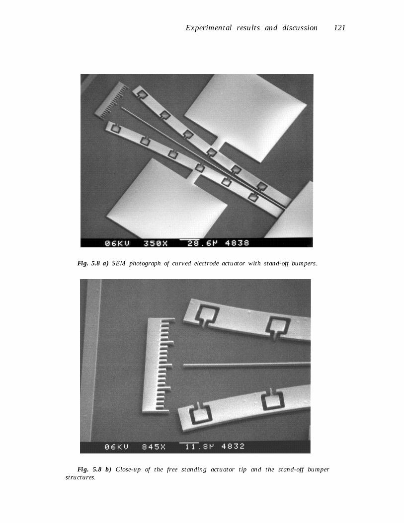
Experimental results and discussion 121
Fig. 5.8 a) SEM photograph of curved electrode actuator with stand-off bumpers.
Fig. 5.8 b) Close-up of the free standing actuator tip and the stand-off bumperstructures.

122 Electrostatic curved electrode actuators
Fig. 5.9 a) SEM photograph of curved electrode actuator with a silicon nitridesidewall insulation.
Fig. 5.9 b) SEM photograph of a microgripper employing curved electrode structuresfor actuation.

Experimental results and discussion 123
curved electrode is connected to a positive voltage. Deflections and dimensionshave been measured using a micrometer eyepiece.
5.5.2 Pull-in voltage of instable bumper designs:
To determine the pull-in voltage, the driving voltage was slowly increaseduntil the beam deflection became unstable. The results are shown fig. 5.10 andthe pull-in voltages are listed in table 5.2. The calculated pull-in voltages asobtained from the energy model are smaller than the measured values. Thedifference is increasing with a decreasing order of the electrode curvature. Thiseffect can be explained by three dimensional electrostatic field effects.
Electrostatic fringing fields will increase the electrostatic forces and willresult in lower pull-in voltages than calculated by our simple parallel plateapproximation. However, the presence of the groundplane gives rise to anunbalanced electrostatic field distribution [5.13]. This effect reduces theelectrostatic forces, especially for large gaps, and induces a levitation of thesurface micromachined structure. The pull-in voltage will increase by thepresence of the groundplane and this effect will be stronger for increasing gapdistances. Therefore it is difficult to give accurate quantitative predictions ofthe pull-in voltage by a simple one-dimensional model and makes 3Dsimulations necessary.
Note that the pull-in voltage is very sensitive to the thickness of thecantilever beam and the initial gap spacing. For instance a change in beamthickness of 0.1 µm results in a change of about 10 percent in the pull-involtage of a second order polynomial design.
Pull-in Voltage VPI [V]
order Cantilever
Exp. Energy
0 223 130
1.0 98 79
2.0 40 37
Table 5.2 Pull-in voltage of polysilicon (Ey=150 GPa) cantilever beams using bumperstructures with a maximum deflection δmax of 30 µm. The measured thickness of the poly layer is4.6 µm (width of the beam), the thickness of the sacr. layer is 1.6 µm. The thickness t of thedifferent beams is 1.6, 1.7 and 1.8 µm and the initial gap is 2.2, 3.2 and 3.3 µm for the 0,1 and 2order polynomial designs respectively.
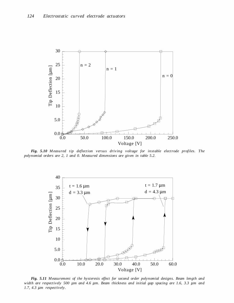
124 Electrostatic curved electrode actuators
0.0
5.0
10
15
20
25
30T
ip D
efle
ctio
n [µ
m]
0.0 50.0 100.0 150.0 200.0
250.0
n = 2n = 1
Voltage [V]
n = 0
Fig. 5.10 Measured tip deflection versus driving voltage for instable electrode profiles. Thepolynomial orders are 2, 1 and 0. Measured dimensions are given in table 5.2.
0.0
5.0
10
15
20
25
30
Tip
Def
lect
ion
[µm
]
35
40
0.0 10.0 20.0 30.0
40.0 50.0 60.0Voltage [V]
t = 1.6 µmd = 3.3 µm
t = 1.7 µmd = 4.3 µm
Fig. 5.11 Measurement of the hysteresis effect for second order polynomial designs. Beam length andwidth are respectively 500 µm and 4.6 µm. Beam thickness and initial gap spacing are 1.6, 3.3 µm and1.7, 4.3 µm respectively.

Experimental results and discussion 125
The behaviour of the actuators show a hysteresis effect for increasing anddecreasing voltages. This has been studied in more detail for the second orderpolynomial electrodes and the experimental results are shown in fig. 5.11. Theorigin of the hysteresis comes from a difference in the electrostatic fielddistribution between a beam before and after pull-in. Once the beam hascollapsed, the electrostatic forces strongly increase as a result of the decreasedgap spacing and a large decrease in the driving voltage is needed beforebending forces overcome the electrostatic forces again.
5.5.3 Constrained bumper designs:
When the polynomial order becomes larger than 2 the deflection of the beambecomes constrained by the geometry of the curved electrode as discussedearlier. The measured deflection behaviour of a third and fourth orderpolynomial curvature design with bumper structures at every 50 µm is shownin fig. 5.12 for beams with a length of 500 µm. The application of bumpersresults in a stepwise behaviour where the cantilever beam reaches an instablepoint from bumper to bumper. In fig. 5.12 also simulated results, as obtainedfrom CoSolve-EM, are shown for the third order design. The model is in fairagreement with the data.
0
5
10
15
20
25
30
0
Tip
Def
lect
ion
[µm
]
50 100 150
n = 3n = 4CoSolve: n = 3
t = 1.7 µm
h = 4.6 µm
d = 3.3 µm
L = 500 µm
50 µm stand-off structure distance
Voltage [V]
Fig. 5.12 Experimental results of curved electrodes with stand off bumper structures where thebeam deflection becomes constrained by the electrode geometry (bumpers). The polynomial ordersare 3 and 4. Also the results of a CoSolve-EM simulation for a cubic electrode design with a gapspacing of 3.1 µm employing bumper structures spaced apart at every 50 µm and 2 µm away fromthe curved electrode are shown.

Experimental results and discussion 126
The CoSolve model is systematically somewhat overestimating theelectrostatic force on the beam. This is probably a result from the suppressionof the levitation of the beam or a too small theoretical Young's modulus.
5.5.4 Constrained sidewall insulator designs:
An example of the measurement results from an actuator with continuoussidewall insulation is shown in fig. 5.13. In contrast to our theoretical results,devices with a continuous sidewall insulator did not show completely stablebehaviour. Fabricated devices show a behaviour that is more or less identicalto the constrained bumper designs. Steplike instable and stable regions are alsoobserved. Furthermore, a large variation in behaviour of identical designs hasbeen observed.
0.0
5.0
10
15
20
25
30
0.0
Tip
Def
lect
ion
[µm
]
20.0 40.0 60.0 80.0 100.0
n = 4L = 300 µm SiN insulation
Voltage [V]
Fig. 5.13 Example of the measured tip deflection as function of the driving voltage for afourth order design with a silicon nitride sidewall layer.
It is suggested that these results are caused by imperfections at the sidewallsurfaces such as surface asperities, and entrapped particles and residuesbetween the electrodes after the fabrication process. A close up of a beam withsilicon nitride sidewall insulation is shown in fig. 5.14. Small protrusionsstrongly affect the behaviour of the actuators and prevent the movable beamfrom smoothly zipping along the curved electrode and act like small bumperswhich leads to instabilities. For successful constrained designs smooth

Experimental results and discussion 127
electrodes surfaces are required. This may be difficult to realise by the proposedfabrication process and is, in general, a fabrication problem for this type ofactuators.
Fig. 4.14 Close-up SEM top-view of a cantilever beam with silicon nitride sidewallpassivation. The presence of relative large surface roughness, residue and particles is suggested toinduce instabilities in the actuator behaviour.
5.6 CONCLUSIONS
An electrostatic actuator design has been presented where a deformablemechanical structure is bent around a fixed curved electrode by means ofelectrostatic forces. Such a design is attractive because relatively largedeflections and force generation can be obtained.
For the shape of the curved electrode simple polynomials have been used. Atheory based upon energy methods is presented to describe the static behaviourof the actuator. Furthermore 3D coupled electromechanical simulations usingCoSolve-EM have been performed. The results from both models are inqualitative agreement with each other. When the beam deflection is notconstrained by the curved electrode geometry, instable behaviour occurs at acertain pull-in voltage and a hysteresis exists to release the structure after pull-in. For polynomial designs, with an order above two, it was found that the

128 Electrostatic curved electrode actuators
beam deflection becomes constrained by the curved electrode geometry beforepull-in occurs. Our models predict completely stable behaviour in thissituation.
Curved electrode actuators have been fabricated from polysilicon by surfacemicromachining techniques using a one-mask process. Electric insulation hasbeen realised by stand off bumper structures between the movable beam andthe fixed electrode or by a silicon nitride sidewall layer. Measurements of non-constrained beam deflections show that the qualitative behaviour of the energymodel is in agreement with theory but that the pull-in voltages are higherthan theoretically predicted. This effect is a result of the presence of agroundplane as shown in 3D coupled electromechanical simulations.
Constrained designs employing bumper structures show a stepwisebehaviour as a result of a number of stable positions at the bumper positions.The static behaviour of these designs has been modelled by CoSolve-Em andwas found to be in fair agreement with experimental data.
Experimental data of samples with a continuous sidewall insulator did notshow stable behaviour up to maximal deflection in contrast to our theoreticalresults. It is suggested that this is caused by imperfections at the sidewallsurfaces, as a result of the fabrication process, which prevent the movable beamfrom smoothly zipping along the curved electrode and act like small bumpersleading to local instabilities.
In practice, curved electrode structures are therefore mainly suited for bi-stable actuator applications such as microswitches, microgrippers, microvalvesand micro pumps.
5.7 REFERENCES
[5.1] R. Jebens, W. Trimmer and J. Walker, Microactuators for aligning optical fibers, Sensorsand Actuators, 20, 1989, pp. 65-73.
[5.2] K. Sato and M. Shikida, Electrostatic film actuator with large vertical displacement,Proc. IEEE Micro Electro Mechanical Systems, Travemunde, Germany, February 4-7, 1992,pp. 1-5.
[5.3] J. Branebjerg and P. Gravesen, A new electrostatic actuator providing improved strokelength and force, Proc. IEEE Micro Electro Mechanical Systems, Travemunde, Germany,February 4-7, 1992, pp. 6-11.
[5.4] M. Elwenspoek, L. Smith and B. Hök, Active joints for microrobot limbs, J.Micromech.Microeng., 2 (1992), pp. 221-223.
[5.5] M. Yamaguchi, S. Kawamura, K. Minami and M. Esashi, Distributed electrostatic microactuator, Proc. IEEE Micro Electro Mechanical Systems, Fort Lauderdale, Florida, U.S.A.,February 7-10, 1993, pp. 18-23.
References 129
[5.6] J. Schimkat, L. Kiesewetter, H.J. Gevatter, F. Arndt, A. Steckenborn and H.F. Schlaak,Moving wedge actuator: An electrostatic actuator for use in microrelay, Proc. 4th Int.Conf. and Exhibition on Micro Electro, Opto, Mechanical Systems and Components,Berlin, Germany, October 19-21, 1994, pp. 989-996.
[5.7] M. Elwenspoek, M. Weustink and R. Legtenberg, Static and dynamic properties of activejoints, Proc. 8th Int. Conf. on Solid-State Sensors and Actuators, Stockholm, Sweden, June25-29, 1995, pp. 412-415.
[5.8] I.H. Shames and C.L. Dym, Energy and finite element methods in structural mechanics,McGraw-Hill, New York, 1985.
[5.9] H. Tilmans and R. Legtenberg, Electrostatically driven vacuum encapsulated polysiliconresonators-Part II, Sensors and Actuators, A45, 1994, pp. 67-84.
[5.10] P. Osterberg, H. Yie, X. Cai, J. White and S. Senturia, Self consistent simulation andmodelling of electrostatically deformed diaphragms, Proc. IEEE Micro ElectroMechanical Systems, Oiso, Japan., February 25-28, 1994, pp. 28-32.
[5.11] J.R. Gilbert, R. Legtenberg and S.D Senturia, 3D coupled electro-mechanics for MEMS:Applications of CoSolve-EM, Proc. IEEE Micro Electro Mechanical Systems, Amsterdam,The Netherlands, January 30-February 2, 1995.
[5.12] R. Legtenberg and H.A.C. Tilmans, Electrostatically driven vacuum encapsulatedpolysilicon resonators-Part I, Sensors and Actuators, A45, 1994, pp. 57-66.
[5.13] W.C. Tang, M.G. Lim and R.T. Howe, Electrostatic comb drive levitation and controlmethod, J. of Micro Electro Mechanical Systems, Vol. 1, 1992, pp. 170-174

130 Electrostatic curved electrode actuators

131
Chapter Six
COMB-DRIVE ACTUATORS FOR LARGEDISPLACEMENTS*
The design, fabrication and experimental results of lateral comb-drive actuators for largedisplacements at low driving voltages is presented. A comparison of several suspensiondesigns is given, and the lateral large deflection behaviour of clamped-clamped beamsand a folded flexure design is modelled. An expression for the axial spring constant offolded flexure designs including bending effects from lateral displacements, which reducethe axial stiffness, is also derived. The maximum deflection that can be obtained bycomb-drive actuators is bounded by electromechanical side-instability. Expressions forthe side-instability voltage and the resulting displacement at side-instability are given.The electromechanical behaviour around the resonance frequency is described by anequivalent electric circuit. Devices are fabricated by polysilicon surface micromachiningtechniques using a one mask fabrication process. Static and dynamic properties aredetermined experimentally and are compared with theory. Static properties are determinedby displacement-to-voltage, capacitance-to-voltage and pull-in voltage measurements.Using a one-port approach, dynamic properties are extracted from measured admittanceplots. Typical actuator characteristics are deflections of about 30 µm at driving voltagesaround 20 V, a resonance frequency around 1.6 kHz and a quality factor of approximately3.
6.0 INTRODUCTION
Comb drive actuators consist of two interdigitated finger structures, whereone comb is fixed and the other one is connected to a compliant suspension.Applying a voltage difference between the comb structures will result in adeflection of the movable comb structure by electrostatic forces. Comb driveactuators have been used as resonators [6.1-6.3], electromechanical filters [6.4],optical shutters [6.5-6.7], microgrippers [6.8] and voltmeters [6.9]. They have alsobeen used as the driving element in e.g. vibromotors [6.10] andmicromechanical gears [6.11].
Voltage controlled comb drive actuators exert a lateral electrostatic forcewhich is independent of position making them attractive for micropositioning applications like, for instance, xy-microstages [6.12-6.14]. Together
* submitted to J. Micromech. Microeng.

132 Comb-drive actuators for large displacements
with nanotools like microtips, integrated systems can be fabricated withapplications in scanning microscopy and data storage [6.15, 6.16]. In mostdevices actuator deflections have been limited to a few microns but in manycases micropositioning over larger distances is attractive. For this reason thedesign and fabrication of large displacement comb drive actuators isinvestigated.
A suspension that is compliant in the aimed direction of displacement andstiff in the orthogonal directions is required. Electrostatic forces increase withdecreasing gap spacing and increasing number of comb fingers. However, dueto fabrication processes, dimensions are limited by minimum feature sizeconstraining e.g. the minimum beam width and gap spacing. These and otherdesign constraints are discussed in order to obtain large-displacement, low-driving-voltage comb-drive actuators.
6.1 SPRING DESIGNS
6.1.1 Introduction
Different types of spring designs have been applied in comb drive actuators[6.1, 6.12, 6.17]. In this section the following spring designs will be discussed;clamped-clamped beams, a crab-leg flexure and the folded beam flexure. Inmost cases, it is desirable to have a structure which is very compliant in onedirection while being very stiff in the orthogonal directions. This can beexpressed as a stiffness ratio. Most polysilicon micromechanical flexuresconstrain motion to a rectilinear direction, and are created from straight beams.When a concentrated load is applied the linear spring constant is defined as:
ki = Fi
δi (6.1)
where Fi and δi are respectively the force and the deflection in the i-direction.The lateral spring constants and stiffness ratio of a clamped-clamped beam, acrab-leg flexure and a folded flexure design will be discussed. The analysisassumes that there is no residual stress present in the spring structures.
6.1.2 Clamped-clamped beam
A clamped-clamped beam with rectangular cross section is shown in fig. 6.1.A concentrated force is applied to the center of the shuttle. The axialdisplacement along the x-axis can be found directly from Hooke's law and the

Spring designs 133
lateral displacement along the y-axis is obtained from small deflection theory[6.18].
X
Y
L
b
anchor shuttle
Fig. 6.1 Clamped-clamped beam.
The spring constants for a concentrated force in x- and y-direction are givenby:
kx =
2 Ey h bL
(6.2)
ky =
2 Ey h b3
L3 (6.3)
where Ey is the Young's modulus, h is the beam width, b is the beam thicknessand L is the length of one beam segment. The stiffness ratio is:
kx
ky
= Lb
2(6.4)
The stiffness ratio of a clamped-clamped beam can be very high. For example,the stiffness ratio is 1.25 105 for a beam with a length of 500 µm and a width of 2µm. For large displacements, however, extensional axial forces develop in thebeam that result in a non-linear force-to-displacement relation. In this casenon-linear effects have to be included that strongly increase the stiffness of thebeam with increasing deflection. This spring design is therefore not suitable forlarge deflections. However, it is useful in applications that requiremeasurement of axial forces; for instance in order to determine residualstresses or measure externally applied axial stresses as in sensing applications.
A derivation of the large deflection behaviour of clamped-clamped beamscan be found in [6.19, Appendix B]. The center deflection for a concentratedload P at the center can be found by simultaneously solving the next equations:
Py =
Ey I b
L3 8/3 u3 32 – 1
2 Tanh2u – 32
Tanh uu
– 12
(6.5)

134 Comb-drive actuators for large displacements
δy = b 2 32 3 u – Tanh u 3
2 – 12 Tanh2u – 3
2Tanh u
u
– 12
(6.6)
with
u = N / EyI
L2
(6.7)
where N is the normal force that develops in the beam as a result of theapplied force and I is the second moment of inertia of the beam. Thenormalised deflection to force behaviour is shown in fig. 6.2. This graph showsthat the small deflection theory is valid for deflections up to about a quarter ofthe beam thickness. For larger deflections non-linear theory has to be used.
0.0
0.5
1.0
1.5
2.0
2.5
3.0
0
δy
/ b
20 40 60 80
Linear
100
PL3/EIb
Fig. 6.2 Normalised deflection of a clamped-clamped beam with dimensions (h*b*2L) of5*2*1000 µm under a force P at the center.
6.1.3 Crab-leg flexure
In order to reduce the extensional axial forces a crab-leg flexure can be used.A sketch of a crab-leg flexure is shown in fig. 6.3. The thigh segment has asecond moment of inertia I1 and a length L1; the shin segment has a secondmoment of inertia I2 and a length L2. The spring constants, as a result of aconcentrated force on the shuttle, in x- and y-direction are given by:

Spring designs 135
X
Y
L1
b L2thigh
shin
Fig. 6.3 Crab-leg flexure.
kx =
12 Ey I2
L23
L1 I2 + 2 L2 I1
2 L1 I2 + L2 I1
(6.8)
ky =
24 Ey I1
L13
L1 I2 + L2 I1
L1 I2 + 4 L2 I1
(6.9)
When the shin and thigh have the same width and thickness, the stiffnessratio can be obtained from:
kx
ky
= 12
L13
L23
L12 + 6 L1 L2 + 8 L2
2
2 L12 + 3 L1 L2 + L2
2(6.10)
Although this design increases the linear deflection region to a certain extent, alarge reduction of the stiffness ratio is introduced. A design that has a shinlength of 50 µm and thigh dimensions equal to our previous clamped-clampedbeam example, has a stiffness ratio that is already several orders of magnitudesmaller. A flexure design that is less susceptible to a decrease in the stiffnessratio is the folded flexure design [1].
6.1.4 Folded flexure
A sketch of the folded beam design is shown in fig. 6.4. The beams areanchored near the center and the trusses allow expansion or contraction of thebeams along the x-axis. The length of the inner and outer beams is identicalotherwise problems may arise because the structure is statically indeterminate.
Assuming rigid trusses, the spring constant of the folded flexure design inaxial and lateral direction can be found from:
kx =
2 Ey h bL
(6.11)
ky =
2 Ey h b3
L3 (6.12)

136 Comb-drive actuators for large displacements
X
Y
Lb
trussFig. 6.4 Folded flexure design.
and the stiffness ratio is:
kx
ky
= Lb
2(6.13)
The folded flexure design strongly reduces the development of axial forces andexhibits a much larger linear deflection range. The stiffness ratio for smalldeflections is equal to the stiffness ratio of a clamped-clamped beam. Thisdesign is therefore very suitable for large deflection actuators. For a moreextensive analysis of folded beams, including the effect of compliant trusses,the reader is referred to [6.20] and [6.21]. The large deflection behaviour of afolded flexure design can be obtained by considering the folded flexure as fourfolded beams in parallel. Each folded beam is a combination of two clamped-guided beams connected in series. By solving the elastica for a clamped-guidedbeam the large deflection behaviour of the folded flexure can be described bythe following set of equations:
δy = 8EyIP
2 p2 Sinφ– 1 dφ
1 – p2 Sin φφ1
π/2
(6.14)
where p can be found from numerical iteration and solving of:
14 L P
EyI=
dφ1 – p2 Sin2 φφ1
π/2
φ1 = ArcSin 2 p2 – 1(6.15)
A detailed derivation of these formulas is given in appendix C. In theseequations p and φ result from a change in variables to bring the equations in

Spring designs 137
the standard form of elliptic integrals. The normalised deflection to forcebehaviour of a folded flexure and cantilever beam is shown in fig. 6.5.
0.0
0.1
0.2
0.3
0.4
0.5
0.6
0 2
δ y /
L
4 6 8 10
Cantilever Beam
Folded Flexure
Linear Theory
LinearTheory
PL2/EyI
Fig. 6.5 Normalised large deflection behaviour of a beam with a length 2L that is clampedat one side and guided along the x-axis at the other end and loaded at its center by a concentratedload P. Assuming rigid trusses the behaviour of such a beam resembles the deflection behaviourof a folded flexure. The deflection of a cantilever beam with a length L loaded at the tip is alsoshown.
The small deflection theory is valid for lateral deflections up to approximately10 percent of the beam length, which is considerably larger than in case of theclamped-clamped beam.
Another important effect that has to be considered is that the stiffness of thefolded beam flexure in the x-direction decreases with increasing displacementin the y-direction. Thus, expressions (6.2), (6.8) and (6.11) are, in fact, upperlimits of the axial spring constants at zero lateral deflection which decreasewith increasing lateral deflection. In order to include lateral deflection effectsin the axial spring constant of the folded flexure the problem is simplified.Because of the folded beam symmetry only one beam segment is considered(see fig. 6.6).
It is assumed that the beam has an initial deflection given by the functionw0(x). The known admissible trial function of the initial deflection profile is:
w0(x) = a x2 6 L – 4 x (6.16)

138 Comb-drive actuators for large displacements
P
L
δbeam
∆
w0(x)
w(x)
Fig. 6.6 Decrease of the stiffness in the x-direction with increasing displacement in the y-direction.
The function of the deflection is approximated by the following admissible trialfunction:
w(x) = b x2 6 L – 4 x (6.17)
where b is an unknown constant. The total potential energy ∏ for the beam is:
Π = 1
2 EyId2 w – w0
dx2
2
dx – P ∆0
L
(6.18)
where P is the axially applied load. The contraction of the beam ∆ can beexpressed as [6.22]:
∆ = 1
2dwdx
2
dx0
L
– 12
dw0
dx
2
dx0
L
(6.19)
After extremisation of the potential energy with respect to b, this contraction isgiven by:
∆ = 3 δbeam
2
5 L1
1 – PPcr
2 – 1 (6.20)
where δbeam is the deflection of the initial beam curvature and the bucklingload Pcr is:
Pcr = 10 E IL2
(6.21)

Spring designs 139
In case of forces that are much smaller than the critical load Pcr (i.e. P/Pcr«1),the axial deflection of a beam segment can be found from:
∆ = 3 P L δbeam2
25 Ey I(6.22)
The spring constant for the folded beam flexure as a result of lateral deflectionscan be found by combining forces and deflections of the beam segmentsresulting in:
kx =
200 Ey I
3 L δy2
(6.23)
From this expression, it can easily be seen that the spring constant in the x-direction decreases with increasing beam displacement in the y-direction. As aresult the stiffness ratio also decreases with increasing lateral beam deflection.The total spring constant is a series connection of the lateral displacementdependant spring constant in eq. (6.23) and the axial spring constant resultingfrom Hooke's law (eq. 6.11).
6.2 ELECTROMECHANICAL BEHAVIOUR
6.2.1 Static behaviour
In the comb actuator a movable set (rotor) and a stationary set (stator) ofcomb fingers are engaged. A ground plane is located under the comb fingerswhich is normally connected to the same potential as the rotor in order toprevent electrostatic pull-down forces to the substrate. An engaged pair offingers, being one cell, of a comb actuator is shown in fig. 6.7. To simplifymodelling the electrostatic field between the rotor and stator is approximatedby a one dimensional parallel plate model between the engaged parts of thecomb fingers. Therefore 3D effects like fringing fields, comb finger end effectsand the groundplane levitation effect are neglected [6.23]. In our case theseeffects will lead to lateral electrostatic forces underestimated by about 5 %, aswill be discussed later.
Lateral deflection
The capacitance between the stator and the rotor can be expressed as:
C =
2 n ε0 h y+y0
d (24)

140 Comb-drive actuators for large displacements
d
y+y0
h
X Z
Y
Fig. 6.7 Cell of engaged comb finger arrays.
where n is the number of fingers, ε0 is the dielectric constant in air, h is theheight of the comb fingers, y0 is the initial comb finger overlap, y is the combdisplacement and d is the gap spacing between the fingers. The lateralelectrostatic force in the y-direction is equal to the negative derivative of theelectrostatic co-energy with respect to y:
Fel = 12
∂C∂y V2 = n ε0 h
dV2 (6.25)
where V is the applied voltage between the stator and the rotor. This force isacting on the spring to which the rotor is connected resulting in a deflection:
y = n ε0 hky d
V2
(6.26)
Side instability
Besides electrostatic forces along the y-axis, electrostatic forces pulling thestator and rotor fingers together are also present. The electrostatic force in theaxial direction is:
Fel =
n ε0 h y+y0
2 d–x2 V2 –
n ε0 h y+y0
2 d+x2 V2 (6.27)

Electromechanical behaviour 141
The forces on both sides of the comb fingers normally cancel each other.However, when the first derivative of the electrostatic force with respect to xbecomes larger than the restoring spring constant in the x-direction a side-instability of the comb drive is introduced. Hence stable comb operation isbounded by:
kx > ∂F
∂x x → 0=
2 n ε0 h y+y0
d3 V2 (6.28)
When the driving voltage exceeds the so-called side-instability voltage VSI thecomb drive becomes unstable leading to side sticking of the rotor and statorfingers. By combining eq. (6.26) and (6.28) the voltage at which side-instabilityoccurs can be expressed as:
VSI
2 =d2 ky
2 ε0 h n2 kx
ky+
y02
d2 –y0
d(6.29)
By neglecting the second term in the root (when kx>>ky), the maximumdeflection ySI that can be obtained before pull-in will occur is:
ySI = d
kx
2 ky–
y0
2(30)
From this equation it can be seen that the side-instability voltage andmaximum deflection are proportional to the gap spacing and increase with thespring stiffness ratio. This shows that comb drive structures with small gapspacings are more susceptible to side instability [6.24] and that spring designswith a large stiffness ratio are preferred for large deflection comb driveactuators. Other sources of instability may result from sideways pull-in ofcompliant fingers themselves and pull-in by the finger front ends when thestator and rotor are almost completely engaged [6.25]. Instabilities have to beavoided by proper design of the comb structure and flexure; and supplytogether with maximum deflection, driving voltage and minimum featuresize, the main constraints on comb actuator design. Large deflection combdrive actuators at low driving voltages should employ compliant springs witha high stiffness ratio and a large amount of comb fingers. In our comb drivedesign a folded flexure has been used which is connected at the center to abeam that is able to hold a large number of comb fingers.

142 Comb-drive actuators for large displacements
6.2.2 Dynamic behaviour
Equation of motion
Using lumped elements the differential equation of motion is given by:
Meq y + α y + ky y = Fel = n ε0 hd
VP + v t2
(6.31)
where M eq is the equivalent mass of the comb drive actuator, α is theequivalent viscous drag parameter and VP is the d.c. polarisation voltage andv(t) the a.c. voltage.
The fundamental frequency
The fundamental frequency of the structure can be obtained from Rayleigh'squotient [6.22]. Using the static deflection profile for the approximatefundamental mode shape function of the beams yields the followingexpression for the fundamental resonance frequency ω0:
ω0 =
ky
Mshuttle + 12 Mtruss + 96
35 Mbeam
(6.32)
where the denominator of the fraction under the root sign resembles theequivalent mass Meq in which Mshuttle is the mass of the shuttle, Mtruss is themass of a single truss and Mbeam is the mass of a single beam. The resonantfrequency is ideally independent of VP and v(t).
Electric Admittance - Equivalent Circuit
If the comb drive is operated in a one-port configuration, the dynamicbehaviour can be described by the electric admittance Y(jω). The voltage ischosen as the independent variable because the electrodes define equipotentialsurfaces making the voltage independent of position. The constitutiveequations of the electrostatic transducer, describing interactions between themechanical and electrical variables can be expressed as:
dqdF
=
2 n ε0 h y0+y00
d2 n ε0 h VP
d
– 2 n ε0 h VP
dky
. dudy
(6.33 a,b)

Electromechanical behaviour 143
where dq is the change in charge on the electrodes, dF is the change inelectrostatic force, du is the change in voltage, dy is the change in displacementand y00 denotes the static deflection caused by the polarisation voltage VP.Combining eq. (6.31) and (6.33a) the admittance is equal to:
Y jω = i
v = jωC0 +jωC1
H jω (6.34)
with
C0 =
2 n ε0 h y0+y00
d(6.35)
C1 = 4 n2 ε0
2 h2 u02
ky d2 (6.36)
H jω =
jωω0
2
+jω
Q ω0+ 1 (6.37)
where C0 and C1 denote the static and motional capacitance, respectively, and Qdenotes the quality factor. An equivalent electrical circuit has been used todescribe the electromechanical behaviour of the comb drive actuator aroundthe resonance frequency. This is shown in fig. 6.8.
Rs
Rp Cp
R1
C1
L1
C0(t)
Fig. 6.8 Equivalent circuit representation of the electrostatic comb drive actuator including
parasitic loads. for C1 see expr. (6.36), L1 = 1ω0
2 C11
ω02 C1
, R1 = 1Q
L1 C1L1 C1
, Cp = parasitic capacitance,
Rp = parallel resistance, and Rs = series resitance .
The corresponding values of resistors, capacitors and inductors can bedetermined by parameter extraction from measured polar admittancecharacteristics [6.26].
144 Comb-drive actuators for large displacements
6.3 FABRICATION
Fabrication starts with a (100) p-type 3" silicon wafer. The first step is wetthermal oxidation at 1150 ˚C to obtain a 2 µm thick SiO2 layer. Next a 5 µmthick polysilicon layer is grown by LPCVD at a temperature of 590 ˚C, apressure of 250 mTorr and a silane flow of 50 sccm. This polysilicon layer isheavily doped with boron by solid source indiffusion at 1100 ˚C for 3 hours.This yields a sheet resistance of about 4.5 Ω/ and also results in a smallresidual strain and strain gradient of the polysilicon layer. After boronindiffusion the BSG layer is stripped in a buffered HF-solution. A 0.6 µm thickPECVD silicon oxide layer is grown that serves as an etch mask for thepolysilicon. After patterning the silicon oxide by RIE using CHF3 gas, thepolysilicon is anisotropically etched using a SF6, O2, CHF3 gas mixture. After acleaning step the sacrificial layer is etched for 50 minutes in a buffered HFsolution. Drying is done by means of a cyclohexane freeze drying method toprevent stiction of free structures to the substrate. Finally a 1 µm thickaluminium layer is evaporated for backside contact. The final result is shownin fig. 6.9-6.12.
6.4 MEASUREMENTS
In the experiments, both the substrate and the rotor electrode were connectedto ground potential while the stator electrode was connected to a positivedriving voltage. From static measurements, flexure spring constants have beendetermined and the Young's modulus of the boron doped polysilicon lateral tothe wafer surface has been calculated. From the dynamic measurements theresonance frequency and quality factor are extracted using the equivalentcircuit parameters.
6.4.1 Extraction of Young's modulus
The displacement as a function of the driving voltage was measured using amicroscope while applying a d.c. voltage between the rotor and thestator/substrate electrodes. Fig. 6.13 shows the results for two crab-leg flexuredesigns. As expected the deflection is proportional to the voltage squared. If theamount of comb fingers, finger thickness and gap spacing are known, thespring constant of the beams can be calculated from the slope of the deflection-

Measurements 145
Fig. 6.9 SEM photographs of fabricated comb drive actuators. The total length of theactuator is about 1 mm.
Fig. 6.10 Close-up view showing the comb finger array, the movable shuttle, the beamanchors and free standing beams. A skeleton structure has been used to enhancesacrificial layer etching.

146 Comb-drive actuators for large displacements
Fig. 6.11 Close-up view of comb fingers of comb structure deflected by electrostaticforces.
Fig. 6.12 Close-up view of comb fingers, truss and deformed beams of a deflected combstructure.

Measurements 147
0
2
4
6
8
10
12
Def
lect
ion
[µm
]
0 100 200 300 400
Voltage2 [V2]
d = 2.6 µm
d = 1.6 µm
Comb structure 30 fingersL1 = 500 µmL2 = 50 µmb = 1.4 µmh = 4.7 µm
front pull-inat 21.5 V
500
front pull-inat 20 V
Fig. 6.13 Measured deflection as a function of the driving voltage for two crab-leg flexuredesigns. The comb consisted of 30 fingers with a gap spacing d of 1.6 and 2.6 µm. The crab-legstructure consisted of a thigh segment with a length L1 of 500 µm and a shin with a length L2 of 50µm. Measured beam width h was 4.7 µm and the beam thickness b was 1.4 µm.
to-voltage curves. The lateral Young's modulus of the polysilicon layer can beextracted from known beam dimensions using the measured spring constant.This yields a lateral Young's modulus of 160±20 GPa for the polysilicon in ourfabrication process. The large uncertainty in this value is mainly a result fromthe measurement error in the beam thickness. The Young's modulus isunderestimated by a small factor because the electrostatic forces are somewhatlarger as a result of fringing fields which have not be taken into account in ourmodel. To obtain an indication of 3D effects, approximate expressions asderived by Johnson and Warne that include fringing fields and groundplaneeffects have been used [6.27]. For comb fingers with a height of 5 µm, a width of2 µm, a gap spacing of 2 µm and a groundplane that is located 2 µm below thefingers, their expression yields an electrostatic force of: Fel = 2.6225 n ε0 V2 . Thisapproximated 3D force is about 5 % larger than the parallel plateapproximation. After correction for 3D effects a final value of 170±20 GPa forthe lateral Young's modulus has been calculated. This value lies well withinthe range of reported values [6.1, 6.28]. It is in good agreement with atheoretically calculated value of 164 GPa, which has been obtained by averagingof well known mono-crystalline properties, over the measured grainorientations in our polysilicon thin films.

148 Comb-drive actuators for large displacements
The measured deflection to voltage behaviour of the folded flexure actuatordesigns is shown in fig. 6.14. The number of comb fingers in these designs hasbeen increased resulting in lower driving voltages. Deflections of about 30 µmare obtained at driving voltages around 20 Volts.
6.4.2 Pull-in measurements
Another way to determine the static behaviour is by measuring thecapacitance of the comb structure as a function of the d.c. bias voltage.Capacitance to voltage measurements have been performed using a HP4194Aimpedance analyser. The change in capacitance of some folded beam designs isshown in fig. 6.15. When the pull-in voltage is reached the comb drivebecomes unstable and the capacitance suddenly changes as shown in the figure.
The measured pull-in voltage and deflection at pull-in for different foldedflexure designs is summarised in table 6.1.
Design fingers VSI [V] δ [µm]
C2-2 136 20.0 39.9
C2-3 105 22.8 39.9
C2-4 88 24.3 39.8
C2-5 74 26.1 39.7
Table 6.1 Measured pull-in voltage and deflection at pull-in for different comb drive designs.The initial finger overlap y0 is 4.6 µm, the gap spacing d is 2.2 µm, the height h of the structuresis 4.8 µm and the thickness b of the beams is 1.5 µm.
The spring constants of the beam in the x- and y-direction can be determinedfrom these measurements; the measured spring constants kx and ky arerespectively 17 N/m and 0.029 N/m. The theoretical values using measureddimensions and Young's modulus, are determined from eq. (6.23) and (6.12),giving respectively kx=19.2 N/m and ky=0.044 N/m.
The measured spring constant along the y-axis is somewhat lower than thecalculated value. This could result from the fact that the trusses are not rigid, asassumed in the theoretical model, or by a non-rectangular cross section of thebeams as a result of underetching. The measured spring constant along the x-
axis is in good agreement with the calculated value. A spring constant asobtained directly from Hooke's law (eq. 6.11), would result in a largeoverestimation of the spring constant in the x-direction yielding a theoreticalvalue forkx that is equal to almost 9000.

Measurements 149
0
5
10
15
20
25
30
Def
lect
ion
[µm
]35
40
0 100 200 300
Voltage2 [V2]
400 500
Design C2-2
Design C2-4
Fig. 6.14 Measured deflection as a function of the driving voltage for several folded flexuredesigns. Design C2-2, C2-4 employed comb structures with respectively 136 and 88 fingers. The gapspacing d equals 2.2 µm and the length of the beams in the folded flexure is 500 µm. The beamwidth h is 4.8 µm and the beam thickness b is 1.5 µm.
0
40
80
120
160
200
0 100 200
∆C
[fF
]
300 400 500 600
Design C2-2Design C2-3
side instability
DC-Bias2 [V2]
Fig. 6.15 Capacitance change of folded beam comb drive designs as a function of the drivingvoltage squared. At a certain voltage pull-in of the comb structure occurs because of sideinstability. Design C2-2 and C2-3 employed comb structures with respectively 136 and 105 fingers.Oher parameters have already been given in fig. 6.13.

150 Comb-drive actuators for large displacements
6.4.3 Frequency response
The admittance of the comb actuators was also measured using the HP 4194Aimpedance analyser. Fig. 6.16 shows the measured and modelled polaradmittance plot of a comb drive actuator around the resonance frequency.Neglecting the series resistance Rs, which has a small contribution compared tothe other admittances, the following parameter values have been extractedfrom a best fit of the measured response: C0+Cp=414.5 fF, C1=145.6 fF, L1=68.4kH, R1=205 MΩ and Rp=17.6 GΩ. This gives a resonance frequency f≈1.60 kHzand a quality factor Q≈3.34.
-3
-2
-1
0
1
2
3
Susc
epta
nce
[nS]
4
-1 0 1 2 3 4
Conductance [nS]
MeasuredModelled
5 6
Fig. 6.16 Measured and calculated admittance of comb actuator C2-2, having a beam length of500 µm, a beam height of 4.8 µm, a beam thickness of 2 µm, a gap spacing of 2.2 µm and 136 combfingers. The d.c. polarization voltage was equal to 15 V and the a.c. drive voltage was equal to0.5V. The dashed line is a theoretical curve using extracted parameter values: C0+Cp=414.5 fF,C1=145.6 fF, L1=68.4 kH, R1=205 MΩ, Rp=17.6 GΩ.
6.5 POSITION CONTROL
An important topic for further work is position control. In micropositioning,position feedback is desirable in order to reduce external disturbances andimprove system response time and accuracy. In xy-stages, for example, springsare mechanically coupled and deflections in one direction may cause small butunwanted deflections in the orthogonal directions. A first study on feedback

Conclusions 151
control of comb drive actuators has been done [6.29, 6.30]. The position caneasily be obtained by measuring the capacitance of the comb drive itself. Thecapacitance of the comb-drive can be measured by the superposition of a highfrequency measurement signal to the driving signal. The measurementfrequency needs to be much higher than the bandwidth of the system. In orderto study control aspects, it is convenient to consider the comb drive actuator asa fourth order system in order to obtain information about feedbacklimitations. The system is generally underdamped; to increase the systemdamping (stability) it is necessary to use e.g. a P(I)D controller. Importantaspects are that single comb drives can only be one-sided controlled and thatthe maximum driving voltage is limited by side-instability of the comb drivewhich put constrains on feedback control.
6.6 CONCLUSIONS
A large deflection, low driving voltage comb drive actuator has beendesigned and fabricated by a one mask fabrication process using boron dopedpolysilicon as the structural material and silicon dioxide for the sacrificialspacer. The lateral Young's modulus of the polysilicon layer has been obtainedfrom static displacement-to-voltage measurements and turned out to beapproximately 170 GPa. Theoretical lateral spring constants of clamped-clamped, crab-leg and folded beam flexure designs have been determined andwere investigated on their large deflection behaviour. Actuator behaviour islimited by electromechanical side instability and expressions for the side-instability voltage and deflection are given. A one-port approach usingelectrostatic excitation and detection to generate and measure dynamicalproperties has been used. The electromechanical behaviour around theresonance frequency was described by an equivalent electric circuit. Themodelled lateral spring constant of the folded beam design was somewhatlarger than experimentally determined values. This is likely to be a result ofcompliant trusses in our fabricated design in contrast to rigid trusses that havebeen assumed in our theoretical model, or by a non-rectangular cross section ofthe beams as a result of underetching. The theoretical axial spring constant of afolded beam which includes a reduction in spring constant with increasinglateral deflection was found to be in good agreement with experimental resultsin contrast to theoretical spring constants simply determined from Hooke'slaw. The electromechanical behaviour can be well described by the presentedequivalent circuit which was used to extract the resonance frequency and

152 Comb-drive actuators for large displacements
quality factor from admittance measurements. An approach towards positioncontrol and feedback was briefly discussed.
REFERENCES
[6.1] W.C. Tang, T.C. Nguyen and R.T. Howe, Laterally driven polysilicon resonantmicrostructures, Sensors and Actuators, 20 (1989), pp. 25-32.
[6.2] R.A. Brennen, A.P. Pisano and W.C. Tang, Multiple mode micromechanical resonators,Proc. Micro Electro Mechanical Systems, Napa Valley, CA, U.S.A. , Feb. 11-14, 1990, pp.9-14.
[6.3] M.W. Judy and R.T. Howe, Polysilicon hollow beam lateral resonators, Proc. IEEE MicroElectro Mechanical Systems, Fort Lauderdale, FL, U.S.A., Feb. 7-10, 1993, pp. 265-271.
[6.4] L. Lin, C.T.C. Nguyen, R.T. Howe and A.P. Pisano, Micro-electromechanical filters forsignal processing, Proc. IEEE Micro Electro Mechanical Systems, Travemünde, Germany,Feb. 4-7, 1992, pp. 226-231.
[6.5] V.P. Jaecklin, C. Linder, N.F. de Rooij, J.M. Moret and R. Vuilleumier, Opticalmicroshutters and torsional micromirrors for light modulator arrays, Proc. IEEE MicroElectro Mechanical Systems, Fort Lauderdale, Florida, U.S.A., Feb. 7-10, 1993, pp. 124-127.
[6.6] O. Tabata, R. Asahi, N. Fujitsuka, M. Kimura and S. Sugiyama, Electrostatic drivenoptical chopper using SOI, Proc. 7th Int. Conf. Solid-State Sensors and Actuators(Transducers '93), Yokohama, Japan, June 7-10,1993, pp. 124-127.
[6.7] P.Y. Chen and R.S. Muller, Microchopper-modulated IR microlamp, Proc. IEEE Solid-State Sensors and Actuators Workshop, Hilton Head Island, SC, U.S.A., June 13-16, 1994,pp. 239-242.
[6.8] C.J. Kim, A.P. Pisano and R.S. Muller, Overhung electrostatic micro gripper, Journal ofMicroelectromechanical Systems, Vol. 1, No. 1, March 1992, pp. 31-36.
[6.9] D.P. Loconto and R.S. Muller, High-sensitive micromechanical electrostatic voltmeter,Proc. 7th Int. Conf. Solid-State Sensors and Actuators (Transducers '93), Yokohama,Japan, June 7-10, pp. 878-881.
[6.10] A.P. Lee and A.P. Pisano, Polysilicon angular microvibromotors, Journal ofMicroelectromechanical Systems, Vol. 1, No. 2, June 1992, pp. 70-76.
[6.11] E.J. Garcia and J.J. Sniegowski Surface micromachined microengine as the driver formicromechanical gears, 8th Int. Conf. on Solid-State Sensors and Actuators (Transducers'95), Stockholm, Sweden, June 25-29, 1995, pp. 365-368.
[6.12] V.P. Jaecklin, C. Linder, N.F. de Rooij, J.M. Moret, R. Bischot and F. Rudolf, Novelpolysilicon comb actuators for xy-stages, Proc. IEEE Micro Electro Mechanical Systems,Travemünde, Germany, Feb. 4-7, 1992, pp. 147-149.
[6.13] V.P. Jaecklin, C. Linder, N.F. de Rooij, Comb actuators for xy-microstages, Sensors andActuators, Vol. A 39, 1993, pp. 83-89.
[6.14] H. Jansen, R. Verhagen and M. Elwenspoek, The black silicon method III: Design rules,modelling, optimisation, and performance of precision position systems for scanning probe,gripping and other MEMS applications, Seminar on Handling and Assembly ofMicroparts, Vienna, Austria, Nov. 14, 1994.
[6.15] J. Brugger, V.P. Jaecklin, C. Linder, N. Blanc, P.F. Indermühle and N.F. de Rooij,Microfabricated tools for nanoscience, J. Micromech. Microeng., Vol. 3, 1993, pp. 161-167.
[6.16] Y. Xu, S.A/ Miller and N.C. MacDonald, Microelectromechanical scanning tunnelingmicroscope, Proc. 8th Int. Conf. Solid-State Sensors and Actuators (Transducers '95),Stockholm, Sweden, June 25-29, pp. 640-643.
[6.17] A.P. Pisano and Y.H. Cho, Mechanical design issues in laterally-driven microstructures,Sensors and Actuators, Vol. A21-A23, 1990, pp. 1060-1064.

References 153
[6.18] J.M. Gere and S.P. Timoshenko, Mechanics of Materials, 2nd ed., Van Nostrand Reinhold(UK) Co. Ltd., 1987.
[6.19] R. Frisch-Fay, Flexible bars, Butterworths (London), 1962.[6.20] M.W. Judy, Micromechanisms using sidewall beams, Ph.D. dissertation, Faculty of
Electrical Engineering and Computer Sciences, University of California at Berkeley, 1994.[6.21] G.K. Fedder, Simulation of Microelectromechanical Systems, Ph.D. dissertation, Faculty
of Electrical Engineering and Computer Sciences, University of California at Berkeley,1994.
[6.22] I.H. Shames and C.L. Dym, Energy and finite element methods in structural mechanics,McGraw-Hill, New York, 1985.
[6.23] W.C. Tang, M.G. Lim and R.T. Howe, Electrostatic comb drive levitation and controlmethod, Journal of Microelectromechanical Systems, Vol. 1, No. 4, Dec. 1992, pp. 170-178.
[6.24] T. Hirano, T. Furuhata, K.J. Gabriel and H. Fujita, Design, fabrication and operation ofsub-micron gap electrostatic comb-drive actuators, Journal of MicroelectromechanicalSystems, Vol. 1, No. 1, March 1992, pp. 52-59.
[6.25] V.P. Jaecklin, C. Linder, N.F. de Rooy and J.M. Moret, Micromechanical comb actuatorswith low driving voltage, J. Micromech. Microeng., Vol. 2, 1992, pp. 250-255.
[6.26] H.A.C. Tilmans, Micromechanical sensors using encapsulated built-in resonant straingauges, Ph.D. dissertation, Faculty of Electrical Enginnering, University of Twente, 1993.
[6.27] W.A. Johnson and L.K. Warne, Electrophysics of micromechanical comb actuators, Journalof Microelectromechanical Systems, Vol. 4, No. 1, March 1995, pp. 49-59.
[6.28] R. I. Pratt, G. C. Johnson, R. T. Howe and J. C. Chang, Micromechanical structures for thinfilm characterization, Proc. Int. Conf. on Solid-State Sensors and Actuators, (Transducers'91), San Fransisco, CA, U. S. A., June 24-27, 1991, pp. 205-208.
[6.29] A.W. Groeneveld, Electromechanical behaviour and study towards position control ofelectrostatic comb drive actuators, Master Thesis, University of Twente, December, 1995.
[6.30] R. Legtenberg, A.W. Groeneveld and M. Elwenspoek, Towards position control ofelectrostatic comb drives, Proc. 6th Workshop on Micromachining Micromechanics andMicrosystems (MME '95), Copenhagen, Denmark, 3-5 September, 1995, pp. 124-127.

154 Comb-drive actuators for large displacements

Chapter Seven
AN ELECTROSTATIC LOWER STATOR AXIALGAP POLYSILICON WOBBLE MOTOR*
This chapter presents the design, modelling, fabrication and first performancecharacteristics of electrostatically driven axial-gap polysilicon wobble motors. Aspectssuch as the gear ratio, torque generation, excitation schemes and torque coverage, normalforces, friction, rotor kinetics and dynamical behaviour are addressed. The fabrication isbased on a four mask process using polysilicon surface micromachining techniques.Three to twelve stator pole wobble motor designs are realised with rotor radii of 50 and100 micrometer. Motors are operated successfully at driving voltages of only a fewVolts and are capable of generating torque's in the nNm range at high electrostatic fields.The motor performance is characterised by gear ratio measurements and measuringstarting and stopping voltages. The motor design and fabrication process are suited tothe integration of gear linkages with respect to mechanical power transmission.
7.0 INTRODUCTION
Initial micromechanical motor design and fabrication attempts have beenaxial-gap architectures because of large estimated driving torques [7.1-7.4].These designs, however, suffered from instabilities in tilting, to a lesser extentin vertical pertubations, and fabrication complexity that finally led to thedevelopment of radial-gap or side-drive micromotors [7.5-7.8]. Salient-pole andwobble side-driven micromotors have successfully been fabricated.
Although the performance of these micromotors is still improving, they doexhibit some drawbacks. The rotor to stator overlap is small, resulting in smalldriving torque's. Typically a few pNm for salient pole micromotors and a fewtens of pNm for wobble motors. This is merely the result of the rotor and statorthickness that is generally only a few microns. Furthermore, it is difficult toimplement the radial gap design into a system with respect to mechanicalpower transmission. In outer stator designs, the stator completely surrounds
* presented at the 8th Int. Conf. on Solid-State Sensors and Actuators (Transducers '95),Stockholm, Sweden, June 25-29, 1995, Vol. 2, pp. 404-407. submitted to Journal ofMicroelectromechanical Systems.

156 Electrostatic lower stator axial gap polysilicon wobble motor
the rotor making it difficult to transfer the mechanical energy to anotherstructure when using planar fabrication techniques. While for inner statordesigns, it is difficult to make the electrical stator connections [7.9, 7.10].
A number of different side-driven wobble motors have been investigated[7.9-7.13]. Wobble motors are able to generate a larger driving torque'scompared to salient pole micromotors because of their gear ratio. The gear ratioincreases the driving torque at the cost of a decreasing angular speed. Also, inwobble motors friction is expected to be lower because of a rolling motioninstead of sliding.
A lower stator axial gap wobble motor design probably can solve some of thelimitations of the radial-gap or side-drive design. This design was firstpresented by Paratte [7.14-7.16]. The tilting-, vertical- and radial rotorinstabilities of this lower stator axial gap design are constrained by the bearingand stator geometry. The larger rotor to stator overlap results in a larger torquegeneration and successful drive of a gear train has already been realised by ahybrid design based on electroplating and assembling techniques [7.17].
In this paper the design, modelling, a fabrication process based on polysiliconsurface micromachining techniques and first performance characteristics ofelectrostatically driven axial-gap lower-stator polysilicon micromotors ispresented. The motor design and fabrication process lend itself for on-chipmicromotor driven micro mechanical systems.
7.1 OPERATION PRINCIPLE
The motor is sketched in fig. 7.1. The rotor is resting in its centre at a pin- orball bearing. When a voltage is applied between the rotor and one of the statorpoles, the rotor will be pulled down towards a contact point at the angularcentre of the excited stator pole.
ωrotorExcited pole
ωstatorFig. 7.1 Sketch of the operation principle.

Theoretical model 157
Switching to other stator poles will move this contact point around and therotor is forced to roll at its outer radius resulting in a rocking motion.
Because of a difference in radius between the rotor and the resulting contactpoint circle, the rotor will be rotated by a small angle after one sequentialactivation of all stator poles. By proper commutation of the charge distributionon the stator electrodes and the rotor, continuous motion of the rotor can beachieved. The ratio between the angular speed of the stator poles and the rotoris called the gear ratio n.
7.2 THEORETICAL MODEL
7.2.1 Gear Ratio
For small rocking angles, in the absence of rotor slip and mechanicaldeformations, the harmonic reduction ratio of the angular velocity betweenthe stator and rotor is given by the nominal gear ratio. The nominal gear ratiois dependent on motor dimensions and can be found from the ratio of therotor radius and the difference between the rotor radius and the contact pointradius. The radius of the resulting contact point circle Rc can be found from:
RC = R2 + d2 + hb – d sinθ (7.1)
where R is the rotor radius, d is the axial gap distance at the rotor centre, hb isthe height of the bearing pin and θ is the angle between the rotor and the statorsurface which is approximately equal to d/R (see fig. 7.2).
dhb
R
θ
Rc
RM
Fig. 7.2 Schematic cross sectional view of the rotor.
This yields the following expression for the nominal gear ratio:

158 Electrostatic lower stator axial gap polysilicon wobble motor
n0 = R
R – RC≈ –
2 R2
2 d hb – d2(7.2)
Note that the gear ratio is negative when Rc is larger than R which means thatthe rotor rotates in a direction opposite to the excitation of the stator poles.
7.2.2 Torque Generation
The tilt angle θ of the rotor is very small. Therefore the electrostatic field canbe assumed to be vertical. Furthermore, fringing fields have been neglectedand the rotor is assumed to be a rigid disk. An analytical model of the torquegeneration based on these assumptions has been shown to be in goodagreement with FEM simulations for other axial gap motors [7.18]. The axialgap spacing g between the substrate and the rotor is equal to:
g = R – r cos ϕ – α sinθ ≈ d 1 – rR cos ϕ – α (7.3)
where r is the radius, ϕ is a variable for the angle and α is the contact pointangle of the rotor. The electrostatic co-energy E'el of an excited stator pole canbe found by integration over the excited stator region from angle ϕ1 to ϕ2 andradius Ri to Ro yielding:
Eel′ = – 1
2 C V2 = – 12
ε0 r dr dϕ
g + dinsεrRi
Ro
ϕ1
ϕ2
V2 (7.4)
where ε0 is the dielectric constant in air, dins is the thickness of the dielectricinsulator between the stator and rotor, εr is the relative dielectric constant ofthis layer and V is the applied voltage. In the absence of rotor slip, the torquegenerated by the motor τmotor can be found from the negative derivative of theelectrostatic co-energy with respect to the rotor angle α:
τmotor = 12
dCdα V2
(7.5)
An example of the single phase torque as function of the rotor angle α isshown in fig. 7.3 for several stator pole designs. Dimensional values are givenin the figure caption. The torque generation can be in the range of nNm atelectrostatic fields of 108 V/m. The maximum torque is generated when the

Theoretical model 159
rotor contact point is located at one of the edges of the excited stator pole. Thedriving torque can be increased by increasing the angular width of the excitedstator poles up to π radians, by reducing the air gap spacing and the thickness ofthe dielectric layer between the rotor and the stator, by increasing the relativedielectric constants and by increasing the rotor diameter. The torque scalesproportional to the third power with motor radius when the gear ratio andelectric field strength are kept constant.
-700
-500
-300
Tor
que
[pN
m]
-100
100
300
500
700
0 π/2 π 3π/2
Alfa [rad]
2π
3 pole4 pole6 pole12 pole
Fig. 7.3 Single phase torque of a 3, 4, 6 and 12 stator pole design as function of the rotor angle.The driving voltage is equal to 100 Volts. The rotor radius R is 100 µm, the axial gap distance d is2 µm, the thickness of the dielectric layer dins between the stator and rotor is 0.2 µm and has arelative dielectric constant of 7.5. The stator outer radius is equal to the rotor radius (Ro=R) andthe inner stator radius Ri is equal to half the rotor radius (50 µm).
7.2.3 Excitation Schemes and Torque Coverage
The stator needs a minimum of three poles in order to generate a drivingtorque. A stator with two poles with an angle of π radians will only result in arocking motion but does not turn the rotor. To ensure a one directionalrotation, a power supply with at least three independent phases is required.Below the independent phases are represented by alphabetical symbols, givenin bold capitals when activated, and normal format when deactivated. Thetotal amount of alphabetic symbols equals the number of stator poles. Theoverall torque generation τcoverage for different driving schemes or excitation

160 Electrostatic lower stator axial gap polysilicon wobble motor
patterns can be found from the enveloping curve of excited stator poles (seefigs. 7.4 and 7.5). The average torque τav can be found from:
τ av = 12π τ coverage
0
2π
dα(7.6)
and the normalised torque ripple τripple is:
τ ripple = τ max – τ min
τ av (7.7)
The output power of the motor can be found from:
Pmotor = τav ωrotor (7.8)
where ωrotor is the angular speed of the rotor.
Open loop
The motor is operated in open-loop drive in our experiments. The simplestcase for motor operation is a sequential excitation of the different stator poleswhich is called "single-pole open-loop excitation" (e.g. Abcd, aBcd, abCd, abcD
etc. for a four stator pole design). In this case the rotor rotates till it reaches thezero torque position at the angular center of the excited stator pole (whenfriction is neglected). Switching to the adjacent stator pole results in aninefficient position with respect to torque generation. This can be improvedwhen using a "double-pole open-loop excitation". In this case two adjacentstator poles are excited simultaneously and in the next step this couple isrotated by one stator pole (e.g. ABcd, aBCd, abCD, AbcD etc. ). Now the startingposition of the rotor is always at the edge of an excited stator couple where thetorque generation is highest. The torque coverage of a four stator pole design incase of single-pole open-loop and double-pole open-loop excitation is shown infig. 7.4.
Closed loop
Closed loop control requires a feedback of the rotor position in order toswitch to the next stator pole at the right moment. Feedback of the rotorposition is not implemented at this point. In case of closed loop control thetorque ripple decreases with an increasing number of stator poles. However themaximum torque also decreases because the capacitor surface of

Theoretical model 161
0
100
200
300
400
500
600
700
0
Tor
que
cove
rage
[p
Nm
]
π/2 π 3π/2 2π
single-pole excitation double-pole excitation
Alfa [rad]
Fig. 7.4 Torque coverage in case of open-loop single-pole and double-pole excitation for a fourpole stator design with dimensions and variables as given in fig. 7.3. The average torque in case ofsingle and double pole excitation is repectively 305 and 204 pNm.
0
100
200
300
400
500
600
Tor
que
Cov
erag
e [p
Nm
]
700
0 π/2 π 3π/2 2π
Alfa [rad]
single pole excitationdouble pole excitation
Fig. 7.5 Torque coverage in case of closed-loop single-pole and double-pole excitation for a fourpole stator design with dimensions and variables as given in fig. 7.3. The average torque for thesingle pole excitation is 313 pNm the average torque for the double pole excitation is 350 pNm.

162 Electrostatic lower stator axial gap polysilicon wobble motor
one stator pole decreases with an increasing number of poles. Bysimultaneously exciting a group of adjacent stator poles the maximum drivingtorque can be increased again. The torque generation in case of "single-poleclosed-loop" and "double-pole closed-loop excitation" is shown in fig. 7.5 for afour stator pole design.
These single and grouped pole excitation schemes require a power supplywith a number of independent phases that equals the number of stator poles.This may be a problem in case of a large number of stator poles which can beovercome by a parallel connection of stator poles. However, the simultaneousexcitation of multiple stator groups will somewhat reduce the torquegeneration.
7.2.4 Normal Forces and Friction
If the friction torque balances the electrostatic torque τmotor generated by themotor, rotor slip is avoided, resulting in a pure rolling motion. In fig. 7.6 forcesand torques are shown when a small part dA of the stator is excited.
ϕ1
ϕ2
zero degreeorientation
αrotor contactpoint
ϕr
dFNeldτang
FNcont
dτ
dτrad
excited stator pole
FNcenRi
Ro
Fig. 7.6 Sketch of the model parameters with forces and torques acting on the rotor.
The axial electrostatic force dFNel is balanced by normal reaction forces at therotor contact point dFNcontact and the center bearing dFNbearing. The electrostaticforce induces a torque dτ=dFNel×r that can be divided in a component dτang inthe angular direction and a component dτ rad in the radial direction. Thenormal bearing force FNbearing and normal contact point force FNcontact can befound from the angular torque balance and the force balance in the normal z-direction by integration of the electrostatic forces over the excited region. This

Theoretical model 163
results in the following expressions for the normal force at the contact pointand the normal force at the center bearing:
FNcontact = – 12 ε0 V2 r2 cos ϕ – α
R g + d0εr
2 dr dϕ
Ri
Ro
ϕ1
ϕ2
(7.9)
FNbearing = – 12 ε0 V2
r R – r cos ϕ – α
R g + d0εr
2 dr dϕ
Ri
Ro
ϕ1
ϕ2
(7.10)
The radial torque τrad can be divided in a component that provides the rockingmotion and a component in the z-direction (perpendicular to the statorsurface) that provides the driving torque of the motor (see fig. 7.7):
τmotor = – 12 ε0 sinθ V2 r2 sin ϕ – α
g + d0εr
2 dr dϕ
Ri
Ro
ϕ1
ϕ2
(7.11)
This expression is equal to eq. (7.5) that was derived earlier. The normal forceat the contact point FNcontact and the normal force at the centerpoint FNbearing areshown in fig. 7.8 for a four stator pole design as function of the contact pointangle.
τrad
τrock
τmotor
Fig. 7.7 Decomposition of radial torque into motor torque and rocking torque.

164 Electrostatic lower stator axial gap polysilicon wobble motor
-3500
-3000
-2500
-2000
-1500
-1000
Forc
e [µ
N]
-500
0
500
0 π/2 π 3π/2 2π
Normal force at bearing
Alfa [rad]
Normal force at contact point
Fig. 7.8 The normal force at the contact point FNcontac t and the normal force at thecenterpoint FNbearing as a function of the rotor contact angle α for a four pole stator design usingthe same parameter values as in fig. 7.3.
Sliding and rolling friction results from two bodies that are respectivelysliding or rolling against each other. The frictional forces are generallydependent on the normal forces between the two bodies. A pure rollingmotion exists when the sliding frictional torque is larger than the electrostatictorque on the rotor. For the motor this no-slip condition is given by:
sgn α FNcontact R µcontact + FNbearing rbearing µbearing – τmotor ≥ 0 (7.12)
where µcontact and µbearing are the sliding frictional coefficients at respectively thecontact point and the bearing.
Fig. 7.8 shows that the normal force at the contact point is very large aroundthe region of the excited stator pole. It even changes sign when the contactpoint reaches a position at the opposite side of the excited stator pole becausethe rotor wants to flip over. In this region the frictional torque as a result of thenormal force at the contact point will be zero. However, there is still africtional torque in this region as a result of the normal force at the bearing.Provided the bearing radius and sliding frictional coefficient at the bearing

Theoretical model 165
are large enough (for example: Rbearing=10 µm and µbearing=0.3) the slidingfrictional torque is still in the same range as the motive torque in this region.An appropriate choice of excitation scheme can be used to sustain continuouslarge normal forces that will prevent rotor slip. For example, an excitationscheme where the step angle is smaller than the totally excited angular region,like in the double pole excitation, will always operate at large normal forces.During normal operation our model suggests that the motor will always workunder no-slip conditions.
7.2.5 Kinetic behaviour
The motion of a point on the rotor is a superposition of three movements. 1:a rotation of the rotor around its center, 2: a circular translation of the centeritself and 3: the rocking motion of the rotor. The position of a fixed point onthe rotor can be described by:
p = RM cosα + r cos α
n +ϕ ex +
RM sinα + r sin αn +ϕ ey +
d 1 – cos α n–1n + ϕ ez
(7.13)
where the radius of the center point rotation RM is given by (see fig. 7.2):
RM = hb dR (7.14)
The kinetic behaviour is complex and the motion is related to a cycloid. Themovement of a point at the outer radius of the motor is shown in fig. 7.9. As aresult of the circular translation of the center, a point at the outer radius of themotor even moves in the opposite direction during short time intervals of awobble cycle. This effect, which is also present in side driven wobble motors, isexaggerated in this figure by using a small gear ratio and may haveconsequences for certain applications of wobble motors.
7.2.6 Dynamic behaviour
The velocity of a point on the rotor can be found from the time derivative ofthe position. From this, the kinetic energy T of the rotor can be obtained:
T = π2 ρ h RM
2 R2 α2 + π4
1n2 ρ h R4 α2 + π
8n–1
n2
ρ h d2 R2 α2 (7.15)

166 Electrostatic lower stator axial gap polysilicon wobble motor
- 5- 5
0
0.5
1
1.5
2
Z
- 2 . 50
2.5
5
X
- 2 . 50
2.5
5- 5
- 2 . 5
0
2.5
5
Y
3D View
- 3 - 2 - 1 1 2 3
0.5
1
1.5
2
Z
0 XSide View
-5 -2.5 0 2.5 5
-5
-2.5
0
2.5
5
-5
-2.5
0
2.5
5
X
Y
Top View
Fig. 7.9 3D-, top- and side-view of the movement of a fixed point at the rotor outer radius inarbitrary units. A small gear ratio of about 11 has been used to clearly show the behaviour.

Theoretical model 167
The first term on the right is due to the motion of the center of the rotor. Thesecond term is a result of the rotation of the rotor and the last term is caused bythe rocking motion of the rotor. From Hamilton's principle [7.19], using theexpressions for the electrostatic co-energy and kinetic energy as given in eqs.(7.4) and (7.15) respectively, the equation of motion for the rotor can be found.When additional terms are added to account for damping mechanisms thisyields:
J α + Cv α + sgn α Cd1 + Cd2 V2 = τmotive α (7.16)
where J is the rotational inertia of the rotor, related to the contact point angle,given by:
J = π ρh R2 RM
2 + R2
2 n2 + n–1n
2 d2
4(7.17)
The rotational inertia of the rotor is mainly determined by its inertia about therocking axes which is represented by the last term on the right hand side of eq.(7.17). The α terms in eq. (7.16) have been added to include dampingmechanisms. As proposed by Tai [7.20] and Bart [7.21] in case of side-drivenmicromotors, the next damping mechanisms have been used: C v is thecoefficient of viscous drag, Cd1 is a constant coulombic friction term whichresults from constant normal forces like adhesion forces and gravity and Cd2 isa voltage dependant coulombic friction term resulting from electrostaticnormal forces as shown before and sgn α is the sign function of angularvelocity which is +1 if α > 0 and -1 if α < 0. For small oscillations around anequilibrium position, the differential equation (7.16) can be linearised. In thatcase the natural oscillating frequency of the rotor ωN can be found from:
ωN =
dτdα α=0
J (7.18)
7.2.7 Viscous Damping
Because of the surrounding gas a damping torque will develop as a result ofviscous drag. The viscous drag torque can be found by solving the Navier-Stokes equations. Because of the complex motion of the rotor this problemcannot be solved easily. Furthermore, realised rotor structures exhibit slots as a

168 Electrostatic lower stator axial gap polysilicon wobble motor
result of the fabrication process. A 3-dimensional FEM fluid analysis of theproblem is therefore required. To obtain an indication of the drag torque astrongly simplified approximation has been used. The rotor is assumed to be athin rigid disk and the contributions due to the edges are ignored. The gas istreated as a continuous medium and is assumed to behave as a Newtonianfluid under laminar flow. The viscous drag forces are assumed to be mainlydue to squeeze film damping in the small gap between the rotor and the statorsurface as a result of the rocking motion of the rotor. With these assumptionsthe problem simplifies to a thin inclined rigid disk that is rotating over ahorizontal surface where only the drag forces in the gap between the disk andthe surface are considered. The rotational axis of the disk is perpendicular tothe surface and the disk rotates with an angular speed equal to that of thecontact point. The shear force dFshear of a small part dA at the bottom of thedisk is given by:
dFshear = µ ω rg dA (7.19)
where µ is the viscosity of air and ω is the angular speed of the disk. Thisinfinitesimal shear force results in a frictional torque τviscous that can be foundby integrating dFshear.r over the rotor surface:
τviscous = µ ω r3
d 1 – rR cosϕ
dr dϕ
0
2π
0
R
= 4 π µR4 ω3 d
(7.20)
In case of a slider bearing a comparable approximation was found to besomewhat lower but accurate within a factor of two with a solution from theNavier-Stokes equations [7.22]. Therefore, the expression above is considered tobe a reasonable estimate of the viscous drag torque on the rotor.
7.3 FABRICATION
Micromotor fabrication is based on a four mask process using polysiliconsurface micromachining techniques which is schematically shown in fig. 7.10.The fabrication starts with a (100) p-type 3" silicon wafer. The first step is thedeposition of a 1 µm thick stress reduced siliconnitride layer (SixNy) by LPCVD

Fabrication 169
from a 70 sccm SiCl2H2 and a 18 sccm NH3 flow at 850 ˚C and a pressure of 200mTorr. The next step is the deposition of a 0.5 µm thick polysilicon layer,grown by LPCVD at a temperature of 590 ˚C, a pressure of 250 mTorr and asilane flow of 50 sccm. This polysilicon layer is heavily doped with boron bysolid source drive-in diffusion for one hour at 1150 ˚C. This yields a sheetresistance of about 70 Ω/ . After boron diffusion the BSG layer is stripped in abuffered HF-solution. After patterning the doped polysilicon layer forms thestator poles (fig. 7.10 a).
Again a 0.5 µm thick stress reduced LPCVD silicon nitride layer is depositedthat serves as an insulator between the stator and rotor. Contact windows areopened in this SixNy layer by RIE in a CHF3/O2 gas mixture in order to makecontact with the stator poles later on (fig. 7.10 b).
Now a 2 µm SiO2 layer is grown by PECVD from a SiH4/N2O gas mixture at300 ˚C, a pressure of 650 mTorr and RF power of 60 Watt (fig. 7.10 c). This layerdefines the gap between the rotor and stator. The ball bearing is now formed byone lithography step and dry etching of the SiO2, the SixNy sandwich layer anddry isotropic underetching of the silicon wafer. This is done by RIE the SiO2
layer using CHF3 at a pressure of 20 mTorr and a RF power of 50 Watt and theSixNy layer by RIE using a CHF3/O2 gas mixture at a pressure of 10 mTorr and aRF power of 75 Watt. The resist layer is removed by O2 plasma ashing and thesilicon is underetched by dry isotropic etching in a SF6/N2 gas mixture at 100mTorr and 50 Watt (fig. 7.10 d). Next a 1 µm thick SiO2 layer is deposited byLPCVD from TEOS at 700 ˚C and a pressure of 400 mTorr (fig. 7.10e). Thebearing clearance is defined by this layer.
Now the rotor is constructed. This starts with the deposition of a 2 µm thickLPCVD polySi layer that is also doped by diffusion as previously described. Theanneal step also reduces the residual stress of the polySi layer. After strippingthe BSG layer in BHF a sheet resistivity of about 6 Ω/ is obtained. The crosssection of a ball bearing like groove at this point is shown in fig. 11.
The motor operation requires a rigid rotor design with respect to verticaldeflections in order to prevent rotor deformation by axial electrostatic forcesand stiction problems between the rotor and stator surface. In order to increasethe stiffness of the rotor a 6 µm thick amourphous silicon layer is deposited bysputtering in Ar. This layer is annealed in a N2 atmosphere at 450 ˚C for 1hour to reduce residual stress [7.23]. A 0.6 µm thick PECVD silicon oxide layer isdeposited that serves as an etch mask for the silicon sandwich layer. Afterpatterning the silicon oxide by RIE using CHF3 gas, the polysilicon isanisotropically etched using a SF6, O2, CHF3 gas mixture (fig. 7.10f) [7.24].

170 Electrostatic lower stator axial gap polysilicon wobble motor
(e)
(f)
(g)
(d)
(c)
(b)
(a)
Fig. 7.10 Processing sequence of the wobble motor. More details are given in the text. (a)LPCVD of SiN, LPCVD and etching of polySi, (b), LPCVD of SiN and contact window etching (c),PECVD of SiO2 (d), RIE of SiO2 and SiN and plasma etching of silicon wafer (e), LPCVD of SiO2(f), LPCVD of polySi, sputtering of Si and anisotropic etching (g) Sacrificial layer etching andbackside metallization.

Fabrication 171
Fig. 7.11 SEM photograph the cross section of a ball bearing like groove. The goodstep coverage of the TEOS silicon dioxide- and polysilicon layer is clearly visible.
Fig. 7.12 SEM photograph of an electrostatic axial gap wobble motor with fourstator poles. The rotor diameter is 200 µm and rotor thickness is 8 µm.

172 Electrostatic lower stator axial gap polysilicon wobble motor
The accumulated layers at the backside are stripped by dry etching, followedby a standard cleaning procedure. The sacrificial layers are etched in an HF(50%) solution for 37.5 min., DI rinsed and spin dried. The last step is theevaporation of a 1 µm Al backside metallization layer (fig. 7.10g). The finalresult is shown in fig. 7.12.
A suitable center pin bearing for the rotor is the flange bearing design [7.25].This, however, requires lithography over the patterned rotor structure. Inorder to prevent problems with photoresist step coverage a ball bearing designhas been used. The ball bearing is, however, not self-aligned like the flangebearing design. But alignment within 1 µm should be possible and is notconsidered to affect the motor performance strongly. At this point noexperimental or theoretical optimisation in order to minimise the rotorthickness has been done. For sufficiently thin rotors or good photoresist stepcoverage a flange bearing design for these type of motors can also be realised.Note that the ball bearing design can also be realised with LIGA or othermoulding and electroplating techniques.
7.4 EXPERIMENTAL
In order to verify micromotor static and dynamic models, it is necessary tomeasure the torque and rotor transient response as it moves from one statorpole to the next. Unfortunately, measurement of the generated torque anddetailed experimental measurement of rotor step transient is difficult forwobble micromotors, since torque measurements require mechanical powertransmission and the rotor displacement associated with a step transient isvery small. Instead the characteristic gear ratio of a wobble motor can be easilymeasured [7.25-7.29]. The gear ratio of a wobble motor is defined as the ratio ofthe electrical excitation frequency to the rotor rotational frequency. Starting andstopping voltages can also be determined from which frictional torque's can beextracted. Starting voltages are measured by increasing the driving voltage andobserving at what voltage a motor starts to rotate. Similarly, the stoppingvoltages are measured by decreasing the driving voltage and observing at whatvoltage the motor operation fails. The motor lifetime was defined as the timeto failure in which a motor could be operated at a fixed driving voltage.
To operate the electrostatic motors a programmable power supply whichcontrols the driving schemes has been realised. The driving frequency of the

Results and discussion 173
square wave signal of four independent output phases can be varied between15 Hz and 10 kHz using the internal clock generator. Higher drivingfrequencies can be obtained by using an external clock generator. Theamplitude of the driving voltage can be set between 0 and 100 V. The powersupply is connected to the bonding pads of the stator poles using a probestation. The movements of the motor are recorded using a microscopic set-upthat includes a camera and video recorder. Rotational speeds can easily bedetermined by video replay, from which the gear ratio is calculated. Single poleexcitation schemes have been used in the measurements unless otherwisestated. Stator designs with a larger number of poles than the number of powersupply phases are driven by symmetrically skipping the additional stator poles.Measurements have been performed in air under semi-cleanroom conditionsafter storage periods of up to several months.
7.5 RESULTS AND DISCUSSION
Table 7.1 shows measured starting and stopping voltages for motors withradii of 100 and 50 µm and four stator poles using a single-pole open-loopexcitation at a frequency of 100 Hz. The effect of the driving frequency, thedriving voltage and operating time on the gear ratio of the wobble motors hasbeen measured. The results are shown in figs. 7.13 to 7.15. Experimentallydetermined gear ratios varied between 130 and 200 for the 50 µm rotor radiusdesigns, and between 600 and 1000 for the 100 µm rotor radius designs. Thelarge variation is due to the high sensitivity of the gear ratio to variations inthe rotor radius as a result of underetching, to variations in the gap spacingand to changes in the bearing height because of etch and thin film non-uniformities.
7.5.1 Starting and stopping voltages
The static and dynamic frictional torque of the motor can be derived fromthe measured starting and stopping voltages (see table 7.1). The gap spacing ofthese samples was measured to be 2.3 µm, and the thickness of the siliconnitride layer was 0.46 µm. The motor will stop when the frictional torqueequals the generated torque. The smallest torque will occur at the transitionpoint of the individually excited stator poles. For the four stator pole designthis transition point is located at approximately -0.2 radians from the angularcenter of the stator poles. From this the static friction is calculated to be equal to

174 Electrostatic lower stator axial gap polysilicon wobble motor
Sample # Radius [µm] Starting Voltage[V]
Stopping Voltage[V]
1 100 6.0 4.4
2 100 8.1 5.9
3 100 8.1 5.1
4 100 7.4 5.6
5 50 13.1 10
6 50 21.9 18.5
7 50 16.7 12.0
8 50 19.9 15.5
Tabel 7.1 Measured starting and stopping voltages of several motors with a four polestator design and rotor diameters of 50 and 100 µm. A single-pole open-loop excitation witha square-wave voltage signal at 100 Hz was used.
500
700
900
1100
1300
1500
Gea
r R
atio
10 100 1000 10000
Sample A, 15 VoltSample B, 10 Volt
Frequency [Hz]
Sample C, 10 Volt
Fig. 7.13 Gear ratio as a function of the excitation frequency, measured for threedifferent micromotors.
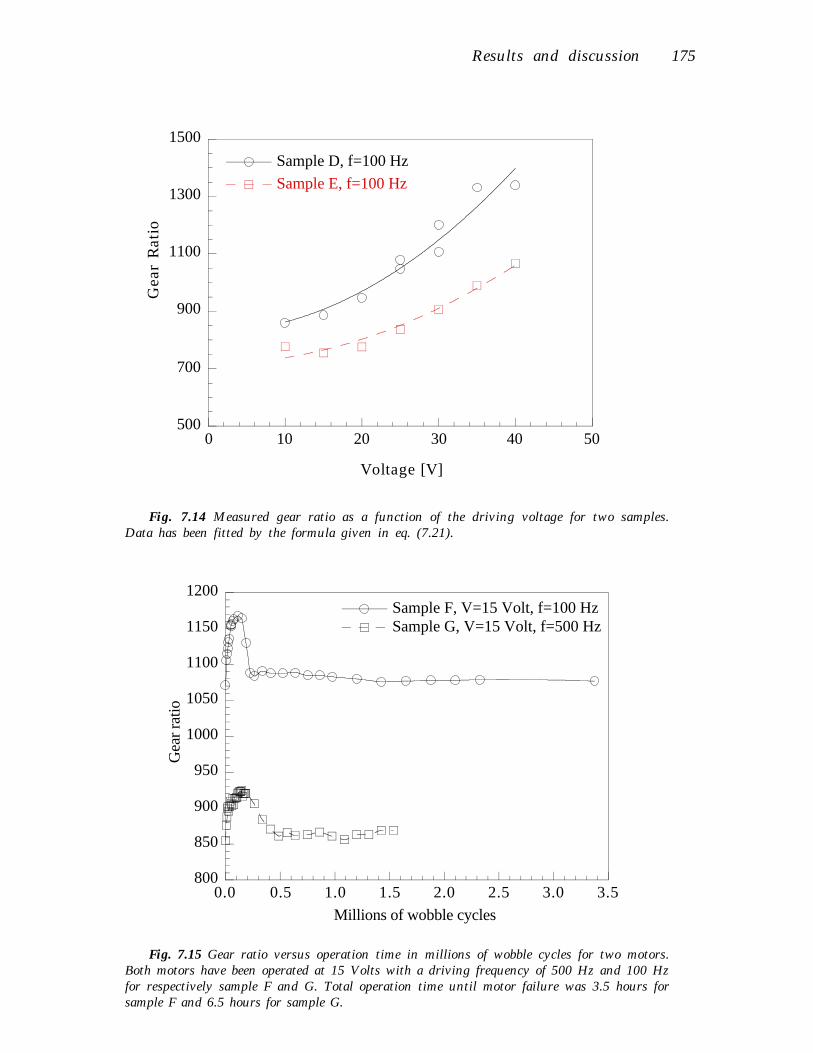
Results and discussion 175
500
700
900
1100
1300
1500
0
Gea
r R
atio
10 20 30 40 50
Sample D, f=100 Hz
Sample E, f=100 Hz
Voltage [V]
Fig. 7.14 Measured gear ratio as a function of the driving voltage for two samples.Data has been fitted by the formula given in eq. (7.21).
800
850
900
950
1000
1050
1100
1150
1200
Gea
r ra
tio
0.0 0.5 1.0 1.5 2.0 2.5 3.0
Millions of wobble cycles
3.5
Sample F, V=15 Volt, f=100 HzSample G, V=15 Volt, f=500 Hz
Fig. 7.15 Gear ratio versus operation time in millions of wobble cycles for two motors.Both motors have been operated at 15 Volts with a driving frequency of 500 Hz and 100 Hzfor respectively sample F and G. Total operation time until motor failure was 3.5 hours forsample F and 6.5 hours for sample G.

176 Electrostatic lower stator axial gap polysilicon wobble motor
0.71 and 0.48 pNm for the four stator pole motors, with rotor radii ofrespectively 50 and 100 micron. In the same way the average torque toovercome the dynamic friction is equal to 0.43 and 0.25 pNm for the small andlarge four stator pole motors respectively. The larger motors have smallerfrictional torque's in contrast to their larger dimensions. This is a somewhatunexpected result. A possible reason may be the larger rocking angle of thesmall motors that leads to more friction at the ball bearing. The individualfrictional forces at the contact point and the bearing of the rotors cannot,therefore, be extracted from these measurements. Rotor designs with identicalrotor diameters but different bearings radii are expected to be more suited forextracting the frictional forces at the contact point and the bearing. Themeasured frictional torques are somewhat lower compared to their side-drivencounterpart [7.25].
7.5.2 Frequency dependency of the gear ratio
The gear ratio as a function of the driving frequency has been measured forthree different motors and is shown in fig. 7.13. Measurements have beenperformed up to a driving frequency of 10 kHz which is the maximumfrequency of the internal clock generator in our power supply. At 10 kHz theangular speed of four pole stator motor designswith a radius of 100 µm is equalto about 150 rpm. Furthermore, gear ratios at higher frequencies are difficult todetermine by our video system. In this case a stroboscope has to beimplemented in our experimental set-up.
Some change in the gear ratio of the motors is present when the drivingfrequency is varied. However the behaviour is not the same for the differentmotors and the variations show little correlation with the driving frequency.The overall picture seems to be that the gear ratio is more or less independentof the driving frequency up to a frequency of 10 kHz.
7.5.3 Voltage dependency of the gear ratio
The voltage dependency of the gear ratio is shown in fig. 7.14. The gear ratioincreases with increasing driving voltage. This behaviour is opposite to thebehaviour of side driven wobble motors where the gear ratio decreases withincreasing driving voltage as a result of a reduction in slip. It was observed thatthe gear ratio decreased somewhat when, instead of a double pole excitation, asingle pole excitation scheme was used. As rotor slip leads to an increase in thegear ratio and double pole excitation will always operate at large normal forces

Results and discussion 177
which exclude rotor slip, another effect must be responsible. Furthermore, ourmodel predicts that the motors will normally operate under no-slip conditions.It is suggested that the axial electrostatic field will result in a deformation of therotor structure. As illustrated in fig. 7.16 this will result in a small decrease ofthe contact point radius which results in an increase of the gear ratio. Motorsthat are excited over a larger region will exhibit a larger deformationexplaining the increase in gear ratio when double pole excitation is used.
λ
Fig. 7.16 Sketch of rotor deformation by axial electrostatic forces. The rotor deformationresults in a decrease of the contact point radius.
The axial electrostatic forces are quadratically dependent on the appliedvoltage. Therefore the measured dependency has been fitted by the followingequation:
n = n0 + γ V2
(7.21)
As shown in fig. 7.14 the experimental data can be fitted well by this equation.A change in gear ratio from 800 to 1500 is related to a change in the contactpoint radius of only 0.05 %. Additional measurements on rotors with differentstiffnesses or coupled electromechanical simulations of the rotor deformationare necessary to verify our suggestion.
7.5.4 Time dependence of the gear ratio
The gear ratio-to-operation time dependency of two motors is shown in fig.7.15. The gear ratio first increases, then decreases and then remains constantwith increasing operation time until motor failure occurs. The initial increaseand subsequent decrease in the gear ratio with operation time is expected toresult from wear at the ball bearing and the surfaces at the contact circle and iscaused by a run-in period. At the end of this period when the surface asperities

178 Electrostatic lower stator axial gap polysilicon wobble motor
have worn off, the gear ratio remains constant till it stops rotating at the setvoltage. The change in gear ratio, as a result of wear, can be expressed by:
n ≈ n0 1 + 2 hb ∆hb
d2 – 2 d hb
–2 hb – d ∆d
d2 – 2 d hb
(7.22)
where ∆hb is the change in bearing length as a result of wear and ∆d is the wearbetween the stator surface and the rotor surface at the contact point. Wear atthe ball bearing will result in a reduction of the bearing length ∆hb and asubsequent change in the axial gap distance. From eq. (7.22) it can be seen thatthis will lead to an increase of the gear ratio. Wear at the contact point circle,from surface roughness asperities at the bottom of the rotor and the statorsurface, will result in an increase of the gap spacing with ∆d. This results in adecrease of the gear ratio.
The time to motor failure showed large variations for the two process runsthat have been done up to now and ranged from several ten thousands up toseveral millions of wobble cycles for different samples. As in side-drivenwobble motors motor failure may be caused by wear particles [7.29]. At thispoint no SEM inspection of operated motors has been done. More work onwear is needed and other bearing designs, as well as other bearing materials,may lead to extended motor lifetime.
7.5.5 Dynamic behaviour
Measurements on the transient response of the rotor have not beenperformed. However, from measured and estimated parameters a theoreticalprediction of the transient response can be given by using the equation ofmotion given in eq. (7.16). The rotational inertia for a rotor with a radius of 100µm is calculated using eq. (7.17) from which a value of 8×10-22 kgm2 is obtained.For an air viscosity of 1.83×10⁻⁵ kg/ms, the viscous damping constant Cv isestimated by eq. (7.20) to be about 3×10-15 Nms. Measurements on side drivenwobble motors showed that coulombic friction is dominated by the voltagedependant term (i.e. Cd1«Cd2 V2). From the measured dynamic frictionaltorque the value of Cd2 is calculated to be 9×10-15 Nm/V2 for the micromotorswith a radius of 100 µm. The generated torque can be calculated for a givendriving voltage from eq. (7.11). For ease of numerical computation, thefunction π/2 arctan(α /10-4) has been used in place of sgn α . The transient

Results and discussion 179
response of a four stator pole motor in case of a single-pole excitation is shownin fig. 7.17.
The response time is strongly dependent on the driving voltage. Because ofcoulombic friction the rotor does not reach the zero torque position of theexcited stator pole but stops at an angle that is dependent on the driving torque.For decreasing driving voltages this stopping angle approaches about -0.2radians as discussed before in the section on starting and stopping voltages.
-2.0
-1.5
-1.0
-0.5
0.0
0.5
1.0
Alf
a [r
ad]
0 20 40 60 80 100
Time [µsec]
10 Volt 30 Volt100 Volt
120 140 160
Fig. 7.17 Transient response of a four stator pole design with single pole excitation for adriving voltage of 10, 30 and 100 Volts. Starting angle is -π/2 radians. R = 100 µm, Ri = 50 µm, Ro =
100 µm, d = 2.3 µm, dins = 0.46 µm, εr = 7.5, ϕ1 = -π/4 rad, ϕ2 = π/4 rad, J = 2.0×10⁻²¹ kgm/s2, Cv =
4.1×10⁻¹⁸ Nms, Cd1 = 0 Nm and Cd2 = 9×10-15 Nm/V2.
7.6 CONCLUSIONS
The design and fabrication of an electrostatically driven lower-stator axial-gap wobble motor has been presented. In contrast to side drive motors, thestator poles are located underneath the rotor instead of surrounding the rotorsides. This results in a higher torque generation and easily accessible rotorstructures that are suited to mechanical power transmission to other structuresthat can be fabricated on the same chip.

180 Electrostatic lower stator axial gap polysilicon wobble motor
Based on small tilt angles, a rigid disk rotor and simplified electrostatic fields,a theoretical model describing the static and dynamic behaviour of the motorhas been given. The torque generation is in the range of nNm at highelectrostatic fields. The torque coverage for different excitation schemes in thecase of both open-loop excitation and closed-loop excitation, which requiresposition feedback, is discussed. Because of large normal forces, generated by theaxial electrostatic field, the motors can be easily operated in no-slip conditionsat all times. The kinetic behaviour is complex and related to a cycloid. A fixedpoint at the rotor even moves opposite to the rotational direction of the rotorduring small time intervals of a wobble cycle. This may have consequences forcertain applications. Based on side-driven micromotor results an equation ofmotion for the rotor has been derived that includes rotational rotor inertia,viscous drag and coulombic frictional terms. The rotational inertia of the rotoris mainly determined by its inertia around the rocking axes.
Fabrication is based on a four mask process using polysilicon surfacemicromachining techniques. Silicon nitride has been used for electricalinsulation between the rotor and stator poles and silicon oxides were used assacrificial layers that have been removed in an HF solution. The rotor andstator poles have been constructed from doped polysilicon. In order to increasethe stiffness of the rotor, it is made from polysilicon and a thick sputteredamorphous silicon film. A new ball bearing design, which is not self-aligned,has been used for the rotor in order to avoid photoresist step coverageproblems.
Motors have been successfully operated at driving voltages of a few Volts.Motor performance has been characterised by measuring the gear ratio andstart and stop voltage measurements using single pole, open-loop excitationswith square-wave voltage signals. Although some variation in gear data hasbeen observed for different motors, the gear ratio seems to be independent ofthe driving frequency up to a maximum measured frequency of 10 kHz. Thegear ratio was found to be strongly dependent on the driving voltage. It issuggested that this is caused by the mechanical deformation of the rotor thatresults from the axial electrostatic forces. The gear ratio was also found to bedependent on operation time showing an initial increase and decrease of thegear ratio after which it remained constant until motor failure. This behaviouris suggested to result from wear at the ball bearing and the surfaces at thecontact point circle. Motor lifetimes varied between a few ten thousand wobblecycles to some millions of wobble cycles for two different process runs. Thisresembles operation times ranging from a few minutes to several hours at

References 181
rotor speeds between a few and several hundred rpm. A theoretical predictionof the transient response of the motor has been given using measured andestimated calculated parameters in the equation of motion.
The presented theoretical and experimental results can be used as aframework for further development of axial-gap micromotors. Wear andmotor lifetime should be especially investigated as well as other bearingdesigns and bearing materials in order to improve motor performance.
REFERENCES
[7.1] W.S.N. Trimmer, K.J. Gabriel and R. Mahadevan, Silicon electrostatic motors, Proc. 4thInt. Conf. on Solid-State Sensors and Actuators, Tokyo, Japan, June 2-5, 1987, pp. 857-860.
[7.2] J. H. Lang, M. F. Schlecht and R. T. Howe, Electric micromotors: electromechanicalcharacteristics, IEEE Micro Robots and Teleoperators Workshop, Hyannis, Masschusetts,Nov. 9-11, 1987.
[7.3] S. F. Bart, T. A. Lober, R. T. Howe, J. H. Lang and M. F. Schlecht, Design considerationsfor microfabricated electric actuators, Sensors and Actuators, 14, 1988, pp. 269-292.
[7.4] T. A. Lober and R. T. Howe, Surface micromachining processes for electrostaticmicroactuator fabrication, Proc. IEEE Solid-State Sensor and Actuator Workshop, HiltonHead Island, SC, U.S.A. June 6-9, 1988, pp. 59-62.
[7.5] M. Mehregany and Y.C. Tai, Surface micromachined mechanisms and micromotors, J.Micromech. Microeng., 1, 1991, pp. 73-85.
[7.6] IC-processed electrostatic micromotors, L.F. Fan, Y.C. Tai and R.S. Muller, Sensors &Actuators, 20, 1989, pp. 41-47.
[7.7] M. Mehregany, S.D. Senturia, J.H. Lang and P. Nagarkar, Micromotor fabrication, IEEETransactions on electron devices, 39, 1992, pp. 2060-2069.
[7.8] L.S. Tavrow, S.F. Bart and J.H. Lang, Operational characteristics of microfabricatedelectric micromotors, Sensors & Actuators, A35, 1992, pp.33-44.
[7.9] T. Furuhata, T. Hirano, L. H. Lane, R. E. Fontana, L. S. Fan and H. Fujita, Outer rotorsurface-micromachined wobble motor, Proc. IEEE Micro Electro Mechanical Systems, FortLauderdale, Fl, U. S. A., February 7-10, 1993, pp. 161-166.
[7.10] K. Deng and M. Mehregany, Outer-rotor polysilicon wobble motors, Proc. IEEE MEMS,Oiso, Japan, January 25-28, 1994, pp. 269-272.
[7.11] W. Trimmer and R. Jebens, Harmonic electrostatic motors, Sensors and actuators, 20(1989), pp. 17-24.
[7.12] S.C. Jacobsen, R.H. Price, J.E. Wood, T.H. Rytting and M. Rafaelof, A design overview ofan eccentric-motion electrostatic microactuator, Sensors and actuators, 20 (1989), pp. 1-16.
[7.13] Operation of microfabricated harmonic and ordinary side-drive motors, M. Mehregany,P. Nagarkar, S. D. Senturia and J. H. Lang, IEEE?
[7.14] L. Paratte and N.F. de Rooij, A rigid ring electrostatic harmonic wobble motor with axialfield, Proc. 6th Int. Conf. Solid-State Sensors and Actuators (Transducers '91), SanFransisco, CA, USA, June 24-27, pp. 890-893.
[7.15] L. Paratte and N.F. de Rooij, A rigid ring electrostatic harmonic wobble motor with axialfield, Proc. 7th International Conference on Solid-State Sensors and Actuators, Abstractsof late news papers, Transducers '93, Yokohama, Japan, June 7-10, 1993, pp. 4-5.
[7.16] L. Paratte and N. F. de Rooij, Electrodeposited electrostatic rigid-rotor wobble motors onsilicon, Sensors and Actuators, A43, 1994, pp. 371-377.

182 Electrostatic lower stator axial gap polysilicon wobble motor
[7.17] L. Paratte, H. Lorenz, R. Luthier and N.F. de Rooy, Miniature gear reduction unit drivenby a silicon electrostatic wobble motor, J.Micromech. Microeng., 2 (1992), pp. 221-223.
[7.18] Ph. Lerch, B. Romanowiwicz, L. Paratte, N. F. de Rooij and Ph. Renaud, Numericalsimulations of planar wobble motors, Sensors and Actuators, A 46-47, 1995, pp. 640-644.
[7.19] I.H. Shames and C.L. Dym, Energy and finite element methods in structural mechanics,McGraw-Hill, New York, 1985.
[7.20] Y. C. Tai and R. S. Muller, Frictional study of IC-processed micromotors, Sensors andActuators, A21, 1990, pp. 180-183.
[7.21] S.F. Bart, M. Mehregany, L.S. Tavrow, J.H. Lang and S.D. Senturia, Electric micromotordynamics, IEEE Trans. Electron Devices, ED-39, 1992, pp. 566-575.
[7.22] F.S. Sherman, Viscous Flow, McGraw-Hill, 1990.[7.23] M.J. van der Reijden, Characterization of RF-sputtered silicon for application in
micromechanics, Master's Thesis, University of Twente, 1995.[7.24] R. Legtenberg, H. Jansen, M. de Boer and M. Elwenspoek, Anisotropic resctive ion etching
of silicon using SF6/O2/CHF3 gas mixtures, J. Electrochem. Soc., 142, 1995, pp. 2020-2028.[7.25] V. R. Dhuler, M. Mehregany and S. M. Phillips, A comparative study of bearing designs
and operational environments for harmonic side-drive micromotors, IEEE Trans. on El.Dev., Vol. 40, No. 11, 1993, pp. 1985-1989.
[7.26] M. Mehregany, S. M. Philips, E. T. Hsu and J. H. Lang, Operation of harmonic side-drivemicromotors studied through gear ratio measurements, Proc. 6th Int. Conf. Solid-StateSensors and Actuators (Transducers '91), San Fransisco, CA, USA, June 24-27, pp. 59-62.
[7.27] S. M. Phillips and M. Mehregany, Effect of rotor slip on the gear ratio of harmonic side-drive micromotors, Sensors and Actuators, A36, 1993, pp. 249-254.
[7.28] V. R. Dhuler, M. Mehregany and S. M. Phillips, An experimental technique and a modelfor studying the operation of harmonic side-drive motors, IEEE Trans. on El. Dev., Vol. 40,No. 11, 1993, pp. 1977-1984.
[7.29] M. Mehregany, S.D. Senturia and J.H. Lang, Friction and wear in microfabricatedharmonic side-drive motors, Proc. IEEE Solid-State Sensor and Actuator Workshop,Hilton Head Island, SC, U.S.A. June 4-7, 1990, pp. 17-22.

183
Chapter Eight
ELECTROSTATIC MICROACTUATORS WITHINTEGRATED GEAR LINKAGES FORMECHANICAL POWER TRANSMISSION*
In this chapter a surface micromachining process is presented which has been used tofabricate electrostatic microactuators that are interconnected with eachother and linked toother movable microstructures by integrated gear linkages. The gear linkages consist ofrotational and linear gear structures and the electrostatic microactuators include curvedelectrode actuators, comb drive actuators and axial gap wobble motors. Themicromechanical structures are constructed from polysilicon. Silicon dioxide was usedas a sacrificial layer and silicon nitride was used for electrical insulation. A cyclohexanefreeze drying technique was used to prevent problems with stiction. The actuators,loaded with various mechanisms, were successfully driven by electrostatic actuation.The work is a first step towards mechanical power transmission in micromechanicalsystems.
8.0 INTRODUCTION
With improving performance and fabrication techniques, micromechanicalactuators are merging into the field of mechanical power transmission fordriving purposes. It has been previously shown that multi-level linkages canbe fabricated by dissolved wafer, bond and assembly techniques [8.1]. Twosilicon wafers are successively processed, aligned and bonded to a glass wafer,and then dissolved in EDP to free micromechanical mechanisms. Otherexamples of assembled devices that transfer mechanical power are magneticmicromotors where Permalloy and PMMA parts are fabricated with sacrificialLIGA techniques which are subsequently assembled with submicrontolerances [8.2]. Axial gap wobble motor have also been fabricated fromelectroplated nickel rotors that were coupled to miniature pinion and geartrains using assembling techniques [8.3].
Devices where mechanical linkages have been integrated with actuator
* presented at the IEEE Micro Electro Mechanical Systems Workshop, San Diego, CA, U.S.A.,Feb. 12-15, 1996, pp. 204-209.

184 Microactuators with integrated gear linkages
fabrication are vibromotors, where a slider is driven by oblique impact ofresonant comb structures [8.4], and a comb-drive based microengine where thelinear motion of comb structures is converted into a rotary motion of anoutput gear by connecting rods [8.5]. These latter processes have the advantageof batch fabrication without the need for assembly of multiple wafersrequiring alignments, bonding etc., or the addition of other separatelyfabricated parts.
In this paper a fabrication process is presented where different types ofsurface micromachined electrostatic actuators are fabricated in one process.These are interconnected and linked to other microstructures using gearmechanisms without the need for assembling techniques. In our previouswork several electrostatic actuators that can generate relatively large forces,torques and displacements have been developed and fabricated using surfacemicromachining techniques. Examples are bi-stable curved electrode actuators[8.6], linear comb drive actuators [8.7] and axial gap wobble motors [8.8].Mechanisms include gear trains, linear gear racks, sliders and springstructures. First experimental results have shown operational actuators andfunctional micromechanisms. For example electrically powered micromotorsdrive gear trains and gear racks. In the latter case a transformation ofrotational into linear motion is obtained.
The fabrication process can be used to study and optimise properties ofmicromechanical gear mechanisms and measure output force or torque ofelectrostatic actuators. Examples are devices for measurements on static anddynamic friction of gear linkages and measurement of micromotor outputtorque.
8.1 DESIGN ISSUES
8.1.1 General design issues
Since the fabrication of the comb drive actuators and curved electrodeactuators is relatively simple and can be done in a one mask fabricationprocess, [8.6, 8.7] this process has been merged into the fabrication process ofthe axial gap wobble motor [8.8]. The micromechanical structures areconstructed from polysilicon. Silicon dioxide has been used as a sacrificiallayer and silicon nitride was used for electrical insulation. A cyclohexanefreeze drying technique is used to prevent problems with stiction.
The operation principle of a lower stator axial gap wobble motor is based on

Design issues 185
an inclined rotor that is supported at its center and rolling on its outer radius.Excitation of stator poles results in an axial rocking motion of the rotor. Thisrocking motion is transformed into a rotational motion because of a smalldifference in the radius of the rotor and its resultant contact point circle at thestator poles. In contrast to polysilicon side drive motors, where stator poles aresurrounding the rotor, the stator poles of the axial gap wobble motor arelocated underneath the rotor. This results in a large torque generation becauseof a large rotor to stator overlap and a readily accessible rotor for mechanicalpower take off. For a more detailed description of the axial gap wobble motorsreference is made to [8.8].
Because the rotor of the axial-gap wobble motor makes an axial rockingmotion and is rolling on its outer radius, some adjustments are necessarywhen external gear teeth are added. By an additional etch step a circularreduction is created in the rotor structure. Now, the rotor will roll on thiscircular reduction and can have an arbitrary outline. The rotor and gears canrotate and rock in axial directions using a ball bearing while for linearmovements a slider bearing was applied using slots that are etched into thesilicon wafer. The motor rocking motion places a constraint on the thicknessof the gears and therefore the gear thickness should be larger than two timesthe thickness of the sacrificial layer below it. In our fabrication process asacrificial layer thickness of about 2 µm and a gear thickness of about 6 µm wasused.
8.1.2 Tooth design
Gears are an efficient way to transmit mechanical power at almost any speedratio desired. Parallel axis gears transmit power with greater efficiency thanany other form of gearing. The most common type of gear is the spur gearwhich has teeth on the outside of a cylinder which are parallel to the cylinderaxis. This type of gear can be fabricated relatively easy using anisotropicetching techniques.
A conjugate tooth shape is needed in order to transform motion withconstant angular velocity. Involute and cycloidal tooth shapes are conjugatetooth profiles. However, cycloid gearing requires center distances to bemaintained in order to obtain conjugate action, where involute profilesmaintain conjugate action even with variations in gear center distances [8.9].
The gear ratio is a constant and can be found from the ratio of gear teethnumbers. It can be applied to all types of gears with conjugate and non-conjugate gear tooth surfaces and corresponds to the ratio between the gear

186 Microactuators with integrated gear linkages
revolutions. Only in cases of conjugate tooth profiles is the velocity ratio equalto the gear ratio. If not, the gears transform rotation with a varyinginstantaneous velocity ratio.
In this first approach no optimisation has been done on gear design. Becauseof limitations in our present mask layout program and pattern generator, gearteeth with a trapezoidal shape have been used. This will negatively affect theperformance of our gears. However, at this stage the main goal is thedevelopment of a fabrication process for integrated electrostatic actuators andgear linkages; and to demonstrate the feasibility of these micromechanical gearlinkages in order to transfer mechanical power.
In our design two different gears have been used. The largest gear has 36teeth and a base radius of 100 µm which also forms the rotor of electrostaticaxial gap wobble motors. Smaller gears have 18 teeth and a base radius of 50µm. The total depth of the gear teeth is 11 µm, the thickness is 6 µm and apressure angle of 20 degrees has been used. In order to ensure properpatterning and etching a minimum clearance of 2 µm between engaged gearteeth and a bearing clearance of 1 µm has been used. As a result, gear backlashwill be relatively large.
8.2 FRICTION AND WEAR
Although some work has been done on aspects like friction, wear andlubrication of micromechanisms [8.10-8.19], many issues with regard totribological properties, design and operation of microsystems are unexploredand need to be investigated. Frictional effects should be minimised by a properbearing design and a suitable gear tooth profile set resulting in a lateral, purerolling motion between gear teeth. The use of low friction materials [8.15, 8.17,8.18] and lubricants [8.20-8.23] seems to be promising applications. However,one should bear in mind that the operation of axial gap wobble motors isbased upon friction between the rotor and stator surface.
The lifetime of gears and micromotors is limited by wear [8.8, 8.10, 8.11].Friction and wear studies using specimen-on disc [8.15, 8.19] have beenperformed and indicate that diamond-like carbon is an attractive materialwith respect to friction and wear properties. The wear mechanism of brittlematerials like DLC, SiO2, Si3N 4 and SCS was found to be dominated byasperity fracture, and wear of polysilicon is dominated by asperity deformation[8.19]. In general wear has been found to follow macroscopic theory, where

Fabrication process 187
materials of highest hardness show the lowest wear rates, and wear rate isdependent on contact pressure.
A problem related to the axial gap wobble motor, is that the rocking motionof the rotor gives rise to axial motions between the rotor teeth and the teeth ofthe gear structure that is driven. This will induce additional frictional forces.The normal force at the tooth surfaces is roughly equal to the excess motortorque divided by the rotor radius. The torque of a motor with a radius of 100µm can theoretically be in the range of nNm, at high electrostatic fields [8.8],leading to normal forces in the 10 µN range. The axial frictional force resultingfrom the rocking motion is a fraction of this normal force after multiplicationby the frictional coefficient of the materials in contact (e.g. 0.3-0.5). This axialfrictional force is small compared to the axial electrostatic forces of the motorwhich are in the range of mN. Therefore friction between gears as a result ofthe rocking motion is not expected to strongly affect motor torque andperformance.
8.3 FABRICATION PROCESS
The fabrication of electrostatic axial gap micromotors, comb drive actuatorsand curved electrode actuators together with integrated gear mechanisms isbased on a seven mask process using polysilicon surface micromachiningtechniques. The process steps are illustrated in fig. 8.1. Starting material is a(100) p-type 3" silicon wafer. First a 1 µm thick stress reduced silicon nitridelayer is deposited by LPCVD. This is followed by the deposition of a 0.5 µmthick LPCVD polysilicon layer. This polysilicon layer is subsequently dopedwith boron by solid source indiffusion for one hour at 1100 ˚C. After boronindiffusion the BSG layer is stripped in a buffered HF-solution and thepolysilicon is patterned to form the stator poles of the motor and groundplanes of electrostatic actuators (mask #1, fig. 8.1a). Now a second stressreduced LPCVD silicon nitride layer with a thickness of 0.5 µm is depositedwhich serves as an insulation layer. In this SixNy layer, contact windows areetched by RIE in a CHF3/O2 gas mixture in order to make electrical contact tothe stator poles and ground planes (mask #2, fig. 8.1b). Next a SiO2 layer isgrown by PECVD with a thickness of 2 µm which defines the air gap spacingbetween the stator and the rotor of the micromotor and partly defines thesacrificial layer of the structures (fig. 8.1c). Local reductions are etched in this

188 Microactuators with integrated gear linkages
d)
Rotor reduction Slider reduction
i)
Spring/Lateral ActuatorSliderRotor
Stator poles
h)
poly-Si
g)
Anchor
f)
SiO2
poly-Si SixNy
SixNy
b)
Stator contact openings
SiO2
c)
e)
Slider slotsRotor bearing
a)
AlGroundplane
Fig. 8.1 (a), (b), (c), (d), (e), (f), (g), (h), (i) Processing sequence for electrostatic actuatorswith integrated gear linkages.

Fabrication process 189
SiO2 layer using a BHF solution to define the circular region on which therotors will roll (mask #3, fig. 8.1d).
The ball bearings and slider slots are formed by RIE etching of the SiO2 layerusing a CHF3 plasma, RIE etching of the SixNy layers using a CHF3/O2 gasmixture and dry isotropic underetching of the silicon wafer in a SF6/N2 gasmixture (mask #4,fig. 8.1e). After this a SiO2 layer with conformal stepcoverage is grown by LPCVD from TEOS to define the bearing spacing of therotor structures (fig. 8.1f). In the silicon dioxide sacrificial layer anchors for theelectrostatic actuators are patterned by etching in BHF (mask #5, fig. 8.1g). Nowa 6 µm thick LPCVD polysilicon layer is deposited that is also doped by boronindiffusion as described before. The boron indiffusion also reduces theresidual stress of the polysilicon layer. After stripping the BSG layer in BHF aresistivity of about 3 Ω square is obtained. A 1 µm thick PECVD silicon oxidelayer is grown that serves as an etch mask for the polysilicon layer andprevents boron outdiffusion in the subsequent annealing step at 1100 ˚C for 3hours in order to reduce stress gradients as a result of the one sided diffusionstep. Backside layers are stripped by dry etching. The silicon oxide is patternedby RIE using CHF3 gas and the polysilicon is anisotropically etched using a SF6,O 2, CHF3 gas mixture [8.16] (mask #6, fig. 8.1h). In order to remove thepolysilicon from the slots in which the sliders have to move, an isotropic etchstep in a SF6/N2 gas mixture is needed in addition to the anisotropic etchwhile other areas are protected by photoresist (mask #7). After a thoroughcleaning procedure the sacrificial layers are etched in concentrated HF for 50min. This is followed by dilution rinsing in DI water, rinsing in isopropanoland rinsing in cyclohexane while preventing the wafers from drying. Nowfreeze drying is used to remove the cyclohexane at a temperature of -10 ˚Cunder a high N2 flow in order to prevent stiction problems [8.17]. The last stepis evaporation of a 1 µm thick aluminum backside layer (fig. 8.1i). The finalresult is shown in fig. 8.2 to 8.10.
8.4 EXPERIMENTAL RESULTS
First experiments have shown that the micromotors can successfully drivegear trains and slider gear racks resulting in, respectively, torque leverage, androtational to linear transformation. Up to now no integratedmicromechanisms that are driven by electrostatic micromotors have beenreported.

190 Microactuators with integrated gear linkages
Fig. 8.2 SEM photograph of an axial gap wobble motor with gear teeth driving asmaller gear wheel. The rotor and the smaller gear have a base radius of respectively100 µm and 50 µm.
Fig. 8.3 Close-up of the gear teeth. The gear teeth have a thickness of 6 µm, a depthof 11 µm and a diametrical pitch of 18.5 µm.

Experimental results 191
Fig. 8.4 SEM photograph of an axial gap wobble motor connected to a gear rackresulting in transformation of the rotational into linear motion.
Fig. 8.5 Close-up of the gear rack. The slider is able to move on its bearing along slotsthat are etched into the wafer.

192 Microactuators with integrated gear linkages
Fig. 8.6 Cross section of a linear slider showing the slots and bearing that guide itsmotion.
Fig. 8.7 Curved electrode actuator for fixing gear position.

Experimental results 193
Fig. 8.8 Motors linked to a gear rack suspended by folded flexures of comb driveactuators. Such structures could be used to measure output torque and motor dynamics.
Fig. 8.9 Close up view of comb drive structure connected to axial gap wobble motorsfrom fig. 8.8.

194 Microactuators with integrated gear linkages
Fig. 8.10 XY-stage fabricated in the same process run.
Fig. 8.11 Close up of the center of the XY stage from fig. 8.10.

Applications 195
Comb drive structures and curved electrode actuators in conjunction withmicromechanical mechanisms have also been driven electrostatically.
Variations in operation characteristics of gears have been observed whichare expected to result from the non-conjugate gear teeth profile that has beenused. Problems such as gear backlash and impact were also noticed which werecaused by etching- and bearing clearances. Furthermore frictional problemswere encountered with large slider structures (up to 2 mm long). Long sliderscould be moved manually by probe needles but did not slide by electricalpowering micromotors. It is suggested that stress gradients clamp long sliderstructures in their bearing slots resulting in frictional forces which are largerthan the output force of the motors. Further experimental work is needed toobtain more quantitative results.
8.5 APPLICATIONS
Specially designed devices with gear linkages can be used to investigatetribological properties and system design aspects of micromechanical gearsystems. The fabricated devices will be used to explore essential features ofthese issues.
For instance, measurements on gear trains that are driven by comb drivestructures using a gear rack can be used to obtain information on frictionalproperties of the gear teeth and bearing. In the same way the frictionalproperties of sliders can be investigated. Gear linkages can also be used todetermine the torque output of electrostatic micromotors by, for example,loading the motor with a spring and measuring the deflection to voltagecharacteristic.
Future applications of integrated actuator systems can be found in areas likemicropositioning, micromanipulation (i.e. pick and place), scanning probemicroscopy, information storage and micro robotics.
8.6 CONCLUSIONS
A micromachining process for the fabrication of electrostatic microactuatorswhich are linked with each other and connected to other movablemicrostructures by integrated gear linkages has been presented. The fabricationis based on polysilicon surface micromachining and sacrificial layer etching
196 Microactuators with integrated gear linkages
techniques. First experimental results show that electrically powered actuatorssuccessfully drive various micromechanisms. The work is a first step towardsmechanical power transmission in micromechanical systems. Mechanicalpower transmission of microactuators may strongly increase the number ofuseful applications and may lead to new possibilities formicroelectromechanical systems.
REFERENCES
[8.1] Y. Gianchandani and K. Najafi, Batch fabrication and assembly of micromotor-drivenmechanisms with multi-level linkages, Proc. IEEE MEMS, Proc. IEEE Micro ElectroMechanical Systems, Travemünde, Germany, Feb. 4-7, 1992, pp. 141-146.
[8.2] T.R. Christenson, J. Klein and H. Guckel, An electromagnetic micro dynamometer, Proc.IEEE Micro Electro Mechanical Systems, Amsterdam, The Netherlands, Jan. 29-Feb. 2,1995, pp. 386-391.
[8.3] L. Paratte, H. Lorenz, R. Luthier and N.F. de Rooij, Miniature gear reduction unit drivenby a silicon electrostatic wobble motor, J.Micromech. Microeng., 2 (1992), pp. 221-223.
[8.4] M.J. Daneman, N.C. Tien, O. Solgaard, A.P. Pisano, K.Y. Lau and R.S. Muller, Linearmicrovibromotor for positioning optical components, Proc. IEEE Micro Electro MechanicalSystems, Amsterdam, The Netherlands, Jan. 29-Feb. 2, 1995, pp. 55-60.
[8.5] E.J. Garcia and J.J. Sniegowski, Surface micromachined microengine as the driver formicromechanical gears, Proc. of the 8th Int. Conf. on Solid-State Sensors and Actuators(Transducers '95), Stockholm, Sweden, June 25-29, 1995, Vol. 1, pp. 365-368.
[8.6] R. Legtenberg, E. Berenschot, M. Elwenspoek and J. Fluitman, Proc. IEEE Micro ElectroMechanical Systems, Amsterdam, The Netherlands, Jan. 29-Feb. 2, 1995, pp. 37-42.
[8.7] R. Legtenberg, A.W. Groeneveld and M. Elwenspoek, Towards position control ofelectrostatic comb drives, Proc. 6th European workshop on micromachining,micromechanics and microsystems (MME '95), Copenhagen, Denmark, Sept. 3-5, 1995, pp.124-127.
[8.8] R. Legtenberg E. Berenschot, J. van Baar, Th. Lammerink and M. Elwenspoek, Anelectrostatic lower stator axial gap wobble motor: Design and fabrication, Proc. of the8th Int. Conf. on Solid-State Sensors and Actuators (Transducers '95), Stockholm,Sweden, June 25-29, 1995, Vol. 2, pp. 404-407.
[8.9] D.W. Dudley, Handbook of practical gear design, McGraw-Hill, New York, 1984.[8.10] K.J. Gabriel, F. Behi and R. Mahadevan, In Situ friction and wear measurements in
integrated polysilicon mechanisms, Sensors and Actuators, A21-A23, 1990, pp. 184-188.[8.11] M. Mehregany, S.D. Senturia and J.H. Lang, Friction and wear in microfabricated
harmonic side-drive motors, Proc. IEEE Solid-State Sensor and Actuator Workshop,Hilton Head Island, SC, U.S.A. June 4-7, 1990, pp. 17-22.
[8.12] M.G. Lim, J.C. Chang, D.P. Schultz, R.T. Howe and R.M. White, Polysiliconmicrostructures to characterize static friction, Proc. IEEE Micro Electro MechanicalSystems, Napa Valley, CA, U.S.A., Feb. 11-14, 1990, pp. 82-88.
[8.13] R. Kaneko, Microtribology related to MEMS, Proc. IEEE Micro Electro MechanicalSystems, Nara, Japan, Jan. 30-Feb. 2, 1991, pp. 1-8.
[8.14] K. Noguchi, H. Fujita, M. Suzuki and N. Yoshimura, The measurement of friction onmicromechatronics elements, Proc. IEEE Micro Electro Mechanical Systems, Nara, Japan,Jan. 30-Feb. 2, 1991, pp. 148-153.

References 197
[8.15] S. Suzuki, T. Matsuura, M. Uchizawa, S. Yura and H. Shibata, Friction and wear studieson lubricants and materials applicable to MEMS, Proc. IEEE Micro Electro MechanicalSystems, Nara, Japan, Jan. 30-Feb. 2, 1991, pp. 143-147.
[8.16] A.P. Lee, A.P Pisano and L. Lin, Normal and tangential impact in microelectromechanical structures, Proc. IEEE Micro Electro Mechanical Systems, Nara, Japan,Jan. 30-Feb. 2, 1991, pp. 21-26.
[8.17] K. Deng and W.H. Ko, A study of static friction between silicon and silicon compounds, J.Micromech. Microeng., Vol. 2, 1992, pp. 14-20.
[8.18] U. Beerschwinger, S.J. Yang, R.L. Reuben, M.R. Taghizadeh and U. Wallrabe, Frictionmeasurements on LIGA-processed microstructures, J. Micromech. Microeng., Vol. 4, 1994,pp. 14-22.
[8.19] U. Beerschwinger, D. Mathieson, R.L. Reuben and S.J. Yang, A study of wear on MEMScontact morphologies, J. Micromech. Microeng., Vol. 4, 1994, pp. 95-105.
[8.20] P. Cléchet, C. Martelet, M. Belin, H. Zarrad, N. Jaffrezic-Renault and S. Fayeulle,Lubrication of silicon micromechanisms by chemical grafting of long-chain molecules,Sensors and Actuators, A44, 1994, pp. 77-81.
[8.21] H. Zarrad, J.M. Chovelon, P. Cléchet, N. Jaffrezic-Renault, C. Martelet, M. Belin, H.Perez and Y. Chevalier, Optimization of lubricants for silica micromotors, Sensors andActuators, A46-47, 1995, pp. 598-600.
[8.22] H. Zarrad, P. Cléchet, M. Belin, C. Martelet and N. Jaffrezic-Renault, The use of long-chain molecules for the lubrication of micromechanisms, J. Micromech. Microeng., Vol. 3,1993, pp. 222-224.
[8.23] K. Deng, R.J. Collins, M. Mehregany and C.N. Sukenik, Performance impact of monolayercoating of polysilicon micromotors, Proc. IEEE Micro Electro Mechanical Systems,Amsterdam, The Netherlands, Jan. 29-Feb. 2, 1995, pp. 368-373.

198 Microactuators with integrated gear linkages

Chapter Nine
ELECTROSTATICALLY DRIVEN VACUUMENCAPSULATED POLYSILICONRESONATORS*
Basic design issues and a fabrication process based on surface micromachiningtechniques for electrostatically driven vacuum encapsulated polysilicon resonators arepresented. A novel freeze drying method, that does not require vacuum equipment, ispresented. Reactive sealing with LPCVD silicon nitride is used to create the evacuatedcavity, resulting in cavity pressures close to the deposition pressure. Design issuesregarding choice of materials, technology and lay-out are discussed. First experimentalresults, including an admittance plot of the one-port resonator and a plot indicating thedependence of the Q-factor on the resonator geometry and ambient pressure arepresented.
9.0 INTRODUCTION
Resonant sensors are very attractive for the precise measurement ofmechanical quantities such as pressure and force. They offer high sensitivityand resolution together with a semi-digital output, i.e., a frequency [9.1-9.4].The central part of the sensor is a vibrating mechanical element called theresonator, which provides the frequency(shift) output.
Surface micromachined resonators, that are operated in a flexural mode ofvibration, have been used by several research groups in the past [9.5-9.7].Without taking special precautions, these resonators suffer from small signalresponses as a result of a low mechanical quality factor. Lowering of thequality factor is a direct consequence of the introduction of a second surface inclose proximity to the resonator surface. This leads to so-called “squeeze film”damping which can be observed for the normal vibrational motion of twoclosely spaced surfaces [9.5, 9 . 8]. Squeeze film damping becomes significant ifthe gap spacing is small compared to the lateral dimensions of the resonator.Evacuating the surroundings would eliminate the above effect. At the sametime, unwanted environmental effects such as changes in the density of the
* published in Sensors and Actuators A, 45 (1994), pp. 57-66.

200 Vacuum encapsulated polysilicon resonators
surrounding medium, humidity and dust are eliminated as well. Thus, theresonator must be placed inside a vacuum housing. This was realized in avery elegant way by Ikeda et al in 1988 [9.9, 9 . 10]. They fabricated singlecrystalline silicon resonators housed locally in on-chip vacuum shells using aself aligned selective epitaxial technology in combination with selectiveanisotropic etching and hydrogen evacuation techniques. The same concept,but based on a different fabrication technology, has been presented by Guckelet al in 1990 [9.11, 9 . 12]. They employed the polysilicon/silicon dioxidesacrificial layer etching technique to realize a similar structure.
This chapter deals with design and processing issues of electrostaticallydriven vacuum encapsulated polysilicon resonators. A discussion of theresonator performance, including a description of the theoretical model isgiven in [9.13]. The fabrication process is based upon the polysilicon/silicondioxide sacrificial layer etch technique. A novel freeze drying procedure,which, as opposed to earlier reports, offers enhanced speed and does notrequire any vacuum equipment, is presented. For the excitation and detectionof the vibration, the emphasis is on a single element or one-port approach[9.14].
9.1 DESIGN ISSUES
9.1.1 Basic Structure
The basic structure of the resonator is shown in fig. 9.1. The resonatorconsists of a prismatic beam with a rectangular cross section and is housed inan evacuated cavity. From an electric view point, the structure defines a four-terminal device. Both the one- [9.6, 9 . 14] and two-port approach [9.5, 9 . 7,9 . 10] can be used for excitation and detection. Details of the electric drivingscheme are presented in reference [13].
Electrostatic excitation and detection has been employed [9.3-9.7]. This isattractive because of its simplicity and compatibility with micromachining-and IC-technologies. The simple structure makes the mechanical properties,and in particular the residual stress, much easier to control. Also, the schemedoes not suffer from disturbing frequency shifts due to thermally-inducedaxial loads. Moreover, no additional transducer materials are required thatwould be necessary for some other drive and detection schemes, such as piezo-electric transduction. Thus, the electrostatic scheme provides an excellent way

Design issues 201
Substrate
Cap
Evacuated cavity
Resonator
Cap
Resonator
Bottom
Substrate
1
2
3
4
Fig. 9.1 Schematic cross section of a vacuum encapsulated flexural beam resonator, depictedas a four-terminal device.
to come to an "all-silicon device", which is attractive to minimize differentialthermal expansion effects.
9.1.2 The Resonator
The static and dynamic characteristics of the resonator are determined by itsin-plane geometry and by its characteristic dimensions perpendicular to theplane [9.4, 9 . 13]. Flexural beam resonators were designed with lengths of 210,310, 410 and 510 µm and widths of 25, 50 and 100 µm. The beam thickness isapproximately 1.5 µm. Furthermore, a beam-to-substrate gap spacing ofapproximately 1.2 µm and a beam-to-cap gap spacing of 1.5 µm were chosen.These dimensions lead to static capacitances (excluding any parasitics) in therange from 0.03-0.3 pF.
Parasitic loads, which are mainly capacitive, have to be kept very low orhave to be compensated for in order to be able to detect the resonance [9.14].The on-chip parasitic loads are mainly determined by the area of the bondingpads and the interconnecting wires. Thus, wire lengths were kept as short aspossible and a relatively small bonding pad area of 150×150 µm2 was used.
Chips, measuring 6×6 mm2, including 12 different resonant structures weredesigned. As a minimum feature size, a rather conservative value of 5 µm wasused. Figure 9.2 shows a typical layout of the resonator. A total number of tenmasks is needed for the fabrication.
"Drop-in's" of electric and mechanical diagnostics were used forcharacterization. They include checks for alignment accuracy, structures tomeasure the sheet- and contact resistances and further, ring- and buckledbeam structures to determine the residual strain [9.15].

202 Vacuum encapsulated polysilicon resonators
1Cap
2Beam
3Bottom
ContactWindow (#9)
CapBoundary (#8)
Anchor (#7)
BeamImplant (#4)
Bottom Implant (#2)
PolysiliconCut (#5)
Metal Pad (#10)
1st Oxide (#3)
2nd Oxide (#6)
A A'
B
B'
Fig. 9.2 Typical resonator layout. The resonator consists of a doubly supported beam. The in-plane beam dimensions are 410 × 100 µm2.
9.1.3 The Sealing Cap
The mechanical stiffness of the sealing cap must be large enough to preventexcessively large deflections caused by the internal vacuum, which may leadto physical contact between the beam and the cap or the substrate. Thus, theupper limit for the cap width is determined by a given maximum deflection.The maximum deflection w o of a clamped rectangular plate with lateraldimensions b×a can be approximated as [9.16]:
wo ≈
0.00260 ∆p a4
D for b > 2a (9.1)
where ∆p is the difference in pressure of the cavity interior and the ambientand D is the flexural rigidity of the plate. The coefficient 0.00260 depends onthe length over width ratio b/a and is within two percent accuracy if this ratiois larger than 2. For a cap thickness of 2.5 µm this leads to an upper limit of the

Technology and materials 203
width of approximately 150 µm if the maximum cap deflection should notexceed 0.5 µm. Finite element analyses of a more realistic cap structure haveindicated an increase of the maximum deflection of 20-30 % due to smallcorrugations that are a result of the fabrication process (e.g. see fig. 9.5h). Thisleads to a smaller value for the upper limit of the width. The cap thicknessused is approximately 2.6 µm, which is sufficient to keep the inwarddeflection after sealing below 0.5 µm for 100 µm wide beams.
9.2 TECHNOLOGY AND MATERIALS
9.2.1 Surface Micro Machining
Surface micromachining is used to fabricate the polysilicon resonantstructures. The technology relies on the construction of mechanical parts froma thin film material in combination with a sacrificial layer thin film which isused as a spacer between the structural parts [9.5, 9 . 17, 9 . 18]. After selectivechemical removal of the sacrificial layer, freely movable members remain.Surface micromachining offers small dimensions and a good dimensionalcontrol, especially in the thickness direction. Furthermore, a very elegant wayto fabricate evacuated cavities by means of surface micromachining techniqueshas recently been presented [9.17, 9 . 19].
9.3.2 Materials
Taking the planar silicon thin film technology as a starting point, the aim isto the develop an "all silicon device". This provides a good thermal matchwith the silicon substrate and further, IC compatible processing. Fabrication isbased on the polysilicon/silicon dioxide sacrificial layer technique.
In order to obtain a high sensitivity of the frequency per unit applied strain,i.e., the gauge factor, slender beams are required with a low residual strain[9.4]. A tensile strain is desired to minimize the chance for buckling. A tensilestrain in the range of 10-100 ppm is considered to be optimal. The residualstress of polysilicon can be well controlled provided that proper depositionconditions and anneal cycles are used [9.15, 9 . 19-9.21]. Polysilicon with a lowtensile strain can be obtained by low pressure chemical vapour deposition(LPCVD) from silane (SiH4) at processing temperatures close to the transitiontemperature from amorphous to (poly)crystalline layers (≈ 580 ˚C [9.21]).Thermal annealing in nitrogen converts the as-deposited built-in compressivestrain into a controllable tensile strain depending on the annealingtemperature [9.15].

204 Vacuum encapsulated polysilicon resonators
The electrodes of the driving capacitor are defined by locally doping thesilicon substrate, the polysilicon beam and the cap. In order to prevent dopingof unwanted places, undoped oxides must be used as the sacrificial layermaterial. Undoped low frequency (50 kHz) plasma enhanced chemical vapourdeposited (PECVD) oxides, provide an acceptable compromise between a goodstep coverage and a high sacrificial layer etch rate. Doping is done by ionimplantation of boron. Boron results in lower sheet resistivities in polysiliconthan phosphorous and shows less segregation at the grain boundaries [9.22].Boron implantation may however affect the mechanical properties of thepolysilicon layer. Electrical insulation of the cap, the resonator and thesubstrate, is achieved using an separating layer of LPCVD silicon nitride. Thelayer also serves as the anchor material for the different polysilicon layers asindicated in fig. 9.3. The capacitance and the conductivity between thedifferent terminals provide a first indication about the integrity of theinsulating layers and whether the beams are free standing or not.
Si3N4
SiO2 poly-Si
Substrate
Beam CapInsulatingAnchors
Substrate
Gaps
Fig. 9.3 Schematic of the electrical insulation between the resonant beam, the substrate andthe cap using silicon nitride anchors; (a) prior to and (b) following the sacrificial layer etch.
9.2.3 Sticking and Freeze Drying
After etching the sacrificial layers in a undiluted (49 %) HF-solution, aspecific drying procedure is required to prevent sticking of the free structuralmembers to the substrate. Standard drying procedures such as dry spinning orair drying produce surface tension forces which cause “pull-down” of the thin

Technology and materials 205
film structures. Once contact has been made, other forces like van der Waalsforces, electrostatic forces, hydrogen bridging, and chemical reactions comeinto play resulting in permanent attachment of the structures to the substrate[9.23-9.25]. An elegant way to solve this so called sticking problem is "freezedrying". The freeze drying method has been developed as a drying method forbiological specimens by Boyde and Wood in 1969 [9.26]. Guckel et al. [9.24] andlater Takeshima et al. [9.27] implemented this technique for sacrificial layeretching of surface micromachined structures. They describe a process wherebya final rinse agent is frozen and subsequently sublimated in a few hours undervacuum conditions.
In this thesis a new and faster freeze drying technique is presented. It doesnot require any vacuum equipment but instead can be performed underatmospheric conditions. Cyclohexane which freezes at about 7 ˚C is used as thefinal rinse agent. Freezing and subsequent sublimation is readilyaccomplished by placing the substrate under a nitrogen flow on a regulatedpeltier element with a temperature below the freezing point. The total timefor the freeze-sublimation process depends on the geometry of the sample andtypically takes 5-15 minutes for the structures described in this chapter.
Details of the cyclohexane rinse-freeze-sublimation procedure are given inchapter 2.
9.2.4 Reactive Sealing
The reactive sealing technique as developed by Burns and Guckel [9.17,9 . 19] is an elegant way to create vacuum-sealed cavities. It exploits thedifference in geometry between the small etch channels and the larger cavitiesto close off the latter by growing a thin film in the channels. Good stepcoverage is favourable for good sealing properties but also results in thedeposition of a thin layer inside the cavity before the etching channels areclosed.
In the case of the electrostatic driving scheme, a material with goodinsulating properties must be chosen. The deposition of electricallyconductive material inside the cavity creates a miniature Faraday cage aroundthe beam prohibiting the build-up of an electric field. The field is essential forelectrostatic excitation and detection. Furthermore, it is preferable to use amaterial with a tensile residual strain in order to minimize the chance forbuckling of the resonator. LPCVD of silicon nitride was chosen as the reactivesealing process.

206 Vacuum encapsulated polysilicon resonators
The residual pressure inside the cavity after sealing is important with respectto the attainable quality factors [9.3, 9 . 4, 9 . 28]. The cavity pressure aftersealing is a function of the processing pressure and temperature, the gas flows,the reaction products and subsequent (out)diffusions. The overall chemicalreaction for the deposition of silicon nitride from dichlorosilane (DCS) and asurplus of ammonia (NH3) is [9.29]:
3 Si2Cl2H2 + (4 + x) NH3 → Si3N4↓ + 6 HCl↑ + 6 H2↑ + x NH3↑ (9.2)
The reaction above clearly indicates that the number of gaseous moleculesincreases. This means that the cavity pressure will be higher than thedeposition pressure whence the etch channels are closed off. According toBoyle Gay-Lussac’s law for an ideal gas, the final cavity pressure pcavity can beexpressed as:
pcavity = pprocess
Vunsealed
Vsealed
To
Tprocess
nright
nleft(9.3)
where T o and T process denote room temperature and the processingtemperature, respectively, Vunsealed/Vsealed denotes the ratio of the volume of thecavity prior to and after sealing, pprocess denotes the processing pressure andnright/nleft denotes the mole ratio of gaseous products and reactants.
To get an idea of the final cavity pressures, a DCS to NH3 flow ratio of 3:4(i.e., x=0) and no subsequent reactions and diffusions after sealing areassumed. For the reaction given by eq. (9.2) the mole ratio equals 12/7. Theratio Vunsealed/Vsealed results in a slight increase of the sealing pressure and is dueto a volume reduction as a result of the inward deflection of the sealing cap.This deflection is generally undesirable and is therefore kept small, resultingin a volume ratio close to unity. For a processing pressure of 200 mTorr (0.26mbar) and a deposition temperature of 800 ˚C, eq. (9.3) predicts a sealingpressure of about 100 mTorr (0.13 mbar). A more dedicated process performedat a pressure of 20 mTorr, a temperature of 850 °C and the same gas flow ratioas indicated above leads to a sealing pressure of approximately 10 mTorr, butexhibits a lower deposition rate. By using a flow ratio DCS:NH3 = 1:3, a surplusof ammonia results (i.e., x=5) and the mole ratio is equal to 17/12. This leadsto a lowering of the final cavity pressure from 100 mTorr to 83 mTorr.Extending the surplus to infinity, results in a final cavity pressure of 58 mTorr.These simple examples indicate that the mole ratio is not the determining
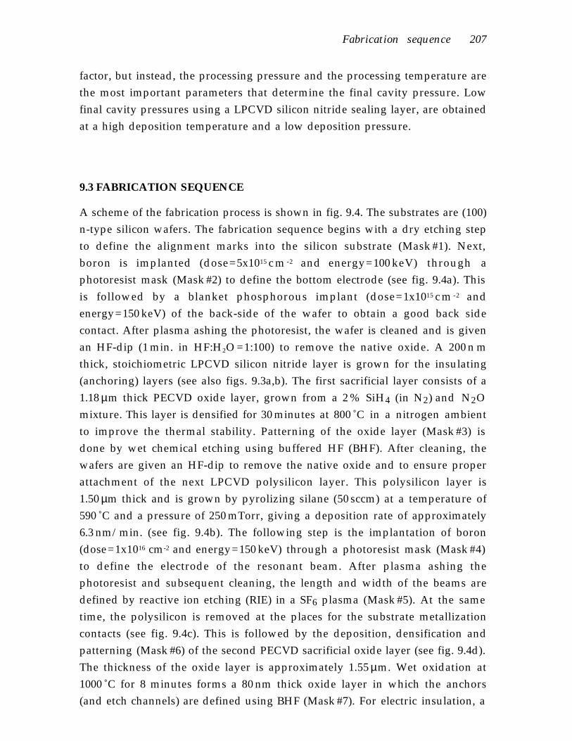
Fabrication sequence 207
factor, but instead, the processing pressure and the processing temperature arethe most important parameters that determine the final cavity pressure. Lowfinal cavity pressures using a LPCVD silicon nitride sealing layer, are obtainedat a high deposition temperature and a low deposition pressure.
9.3 FABRICATION SEQUENCE
A scheme of the fabrication process is shown in fig. 9.4. The substrates are (100)n-type silicon wafers. The fabrication sequence begins with a dry etching stepto define the alignment marks into the silicon substrate (Mask #1). Next,boron is implanted (dose=5x10¹⁵ c m -2 and energy=100 keV) through aphotoresist mask (Mask #2) to define the bottom electrode (see fig. 9.4a). Thisis followed by a blanket phosphorous implant (dose=1x10¹⁵ c m -2 andenergy=150 keV) of the back-side of the wafer to obtain a good back sidecontact. After plasma ashing the photoresist, the wafer is cleaned and is givenan HF-dip (1 min. in HF:H2O =1:100) to remove the native oxide. A 200 n mthick, stoichiometric LPCVD silicon nitride layer is grown for the insulating(anchoring) layers (see also figs. 9.3a,b). The first sacrificial layer consists of a1.18 µm thick PECVD oxide layer, grown from a 2 % SiH4 (in N2) and N2Omixture. This layer is densified for 30 minutes at 800 ˚C in a nitrogen ambientto improve the thermal stability. Patterning of the oxide layer (Mask #3) isdone by wet chemical etching using buffered HF (BHF). After cleaning, thewafers are given an HF-dip to remove the native oxide and to ensure properattachment of the next LPCVD polysilicon layer. This polysilicon layer is1.50 µm thick and is grown by pyrolizing silane (50 sccm) at a temperature of590 ˚C and a pressure of 250 mTorr, giving a deposition rate of approximately6.3 nm/min. (see fig. 9.4b). The following step is the implantation of boron(dose=1x1016 cm-2 and energy=150 keV) through a photoresist mask (Mask #4)to define the electrode of the resonant beam. After plasma ashing thephotoresist and subsequent cleaning, the length and width of the beams aredefined by reactive ion etching (RIE) in a SF6 plasma (Mask #5). At the sametime, the polysilicon is removed at the places for the substrate metallizationcontacts (see fig. 9.4c). This is followed by the deposition, densification andpatterning (Mask #6) of the second PECVD sacrificial oxide layer (see fig. 9.4d).The thickness of the oxide layer is approximately 1.55 µm. Wet oxidation at1000 ˚C for 8 minutes forms a 80 nm thick oxide layer in which the anchors(and etch channels) are defined using BHF (Mask #7). For electric insulation, a
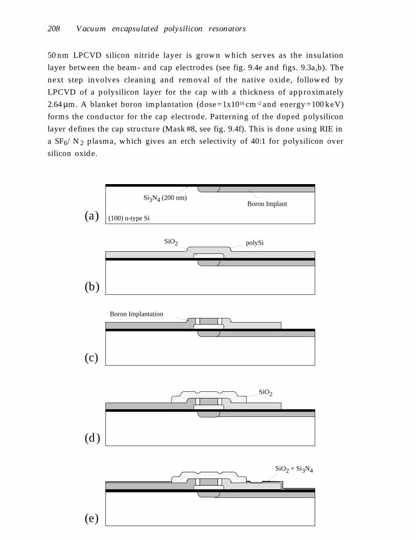
208 Vacuum encapsulated polysilicon resonators
(100) n-type Si
Boron ImplantSi3N4 (200 nm)
(a)
Boron Implantation
(c)
SiO2
(d)
SiO2 polySi
(b)
SiO2 + Si3N4
(e)
50 nm LPCVD silicon nitride layer is grown which serves as the insulationlayer between the beam- and cap electrodes (see fig. 9.4e and figs. 9.3a,b). Thenext step involves cleaning and removal of the native oxide, followed byLPCVD of a polysilicon layer for the cap with a thickness of approximately2.64 µm. A blanket boron implantation (dose=1x1016 cm-2 and energy=100 keV)forms the conductor for the cap electrode. Patterning of the doped polysiliconlayer defines the cap structure (Mask #8, see fig. 9.4f). This is done using RIE ina SF6/N2 plasma, which gives an etch selectivity of 40:1 for polysilicon oversilicon oxide.

Fabrication sequence 209
Si3N4Vacuum
(g)
CapResonator
Bottom Electrode
Contact
(h)
polySi
(f)
Resonator Implant
Gapsdoped Poly-Si
undoped Poly-Si
Si3N4 insulating layers Bottom Electrode
(i)
Metallization
Cap
Beam
Al
Fig. 9.4a-i Processing sequence for sealed polysilicon resonators. The differentstages of the process are explained in the text. 9.4a-h : cross-sectional view B-B’ and9.4i: cross-sectional view A-A’ of fig. 9.2.

210 Vacuum encapsulated polysilicon resonators
The etching is stopped as soon as the underlying silicon nitride and siliconoxide double layer of the etch channels is exposed. From this point on, thickphotoresist layers (3 µm) have to be used to ensure sufficient step coverage.Annealing in a nitrogen ambient for 1 hour at a temperature of 1000 ˚C isnecessary for the electric activation of the implanted boron and moreover, toobtain a low tensile strain in the polysilicon layers. Following a thoroughcleaning step, the sacrificial layer etch and subsequent freeze drying procedureis performed. Sacrificial layer etching is done in an undiluted (49%) HF-solution and takes about two hours. Quenching in DI-water is done for30 minutes and next IPA is added. The wafers are rinsed for 1 hour in an IPAsolution, followed by a final rinse cycle in cyclohexane for 1 hour. Next, thefreeze drying is carried out as described in the previous section (see fig. 9.4g).The mechanical test structures can now be examined to check whether themechanical stress is in the region of interest and whether sacrificial layeretching and freeze drying have been successful. LPCVD of approximately200 nm stoichiometric silicon nitride is used to close off the etch channels. Thesurface passivation of the pn-junction of the bottom electrodes in the substrateis important. Dry thermal oxidation is the best way to accomplish this, butexperiments revealed buckled beams even after growing oxide layers as thin as10 nm at a temperature of 800 ˚C. It was found that the leakage currents of thepn-junctions that are passivated with silicon nitride are on the order of10 µA/cm2, which is considered to be satisfactory. The contact windows for thesubstrate-, beam- and cap electrodes are defined using RIE in a CHF3/O2
plasma (Mask #9). Metallization consists of a 1 µm thick aluminum layer.Prior to the metallization, the thin films that have accumulated on thebackside of the wafer are stripped by means of RIE in a SF6 and CHF3 plasmas.Metal patterning (Mask #10) is done by wet chemical etching. The final step isa 5 minutes anneal in a N2/H2O ambient at 450 ˚C to obtain good ohmiccontacts. Final cross sections of the sealed resonator are shown in figs. 9.4h and9.4i.
9.4 RESULTS
The SEM photograph of fig. 9.5a shows a top view of a sealed resonator. Toinspect the inside of the cavity for residues, and check whether or not thebeams are free standing, caps have been manually removed. This was done bypeeling off a carefully attached tape. The cavity inside turned out to be cleanand displayed free standing beams having smooth surfaces (see figs. 9.5b,c).

First results 211
Fig. 9.5 (a) SEM photograph of a sealed polysilicon resonator.
Fig. 9.5 (b) Resonator with cap removed showing cavity interior.

212 Vacuum encapsulated polysilicon resonators
Fig. 9.5 (c) Close up of cavity interior.
Fig. 9.5 (d) Magnified view of part of the cross section.

First results 213
Cross-sectional views of the resonator are shown in fig. 9.5d. These SEMphotograph clearly indicate (part of) the free standing beam and the shape ofthe cap (compare fig. 9.4h).
9.4.1 Electrical and Electromechanical Behaviour
Electrical measurements indicated sheet resistances of 24 Ω/square,30 Ω/square and 22 Ω/square for the bottom electrode, the resonator electrodeand the cap electrode, respectively. The contact resistance turned out to beabout 1 Ω for a 20×20 µm 2 contact for all three electrodes. Standard I-Vmeasurements used to check the integrity of the nitride insulating anchorsrevealed high ohmic (GΩ’s) anchors. The residual strain has been extractedfrom the polysilicon ring and buckled beam diagnostics and is within therange from -8×10⁻⁷ (compressive) to +6×10⁻⁵ (tensile).
First tests aimed at finding the resonance frequency have indicated that caremust be taken with respect to probing the samples. Static charges induceelectric forces that cause “pull-in” of the beams, resulting in permanentattachment of the latter to the cap or to the substrate. This phenomenon wasobserved while testing uncapped resonators.
-0.2
0.2
0.6
1.0
1.4
1.8
Con
du
ctan
ce G
[µS
]
Susc
epta
nce
B [
µS]
-0.2
0.2
0.6
1.0
1.4
1.8
317000 320250 323500 326750 330000
G
Frequency [Hz]
B
Fig. 9.6 Admittance Bode plot of an electrostatically driven vacuum encapsulatedpolysilicon resonator in a one-port configuration [9.13]. Resonator dimensions are 210×100×1.5 µm.The observed resonant frequency is 323,682 Hz.

214 Vacuum encapsulated polysilicon resonators
Figure 9.6 shows a typical example of a measured Bode plot showing theconductance and the susceptance as a function of the driving frequency of a210 µm long polysilicon beam resonator.
9.4.2 Quality factor and sealing pressure
Vacuum sealing provides pressures in the molecular regime, where the gasmolecules are not interacting with each other. Energy losses due to viscousdamping are negligible in this pressure regime. The damping mechanismsthat remain, include losses due to individual collisions of the gas moleculeswith the resonating surfaces (momentum damping), losses into the mountand intrinsic (material) damping. If momentum damping is considered to bethe dominant loss mechanism and if the resonator was operating in freespace, the mechanical quality factor as a function of the ambient pressure p canbe expressed as [9.28]:
Qn =
3
8 6
αn2
phl
2 πEρRTM
(9.4)
where αn is a constant depending on the edge conditions and on the mode ofvibration n (α 1 = 4.73 for a clamped-clamped beam), h and l are the thicknessand the length of the resonator, respectivley, E and ρ are the Young’s modulusand the specific mass of the resonator material, respectively, R (≈8.31 JK-1mol-1)is the universal gas constant, T is the absolute temperature and M is themolecular mass of the gas. The mechanical quality factor of the one-portresonators can be extracted from the measured Bode-plot and turned out to bea function of the resonator length. It is noted that the quality factor variedacross the wafer, probably as a result of variations of the sealing pressure.
In order to measure the quality factor as a function of pressure, a leak mustbe introduced to the cavity. Fracturing the cap is not considered to be the bestsolution, since this would remove the upper gap and thus would givemisleading results if effects such as squeeze film damping are significant.Therefore, an especially designed “dual cavity structure” has been used tomeasure the quality factor as a function of the pressure inside the cavity. Thestructure consists of two cavities that are interconnected through a narrowchannel. One cavity houses the resonator. By fracturing the other cavity andplacing the structure in a vacuum chamber, the pressure of the cavitycontaining the resonator could be regulated by the external vacuum system.This way, the resonator is still sandwhiched between two air gaps, and thus

First results 215
forms a realistic representation of the actual situation. The results are shownin fig. 9.7. The graph indicates that the quality factor is inversely proportionalto the pressure (as predicted by eq. (9.4)) in the range from 0.01 to 1.0 mbar.This suggests that in this pressure regime, momentum damping is thedominating loss mechanism. However, measured Q-values are more thanone order of magnitude smaller than predicted and some form of “enhancedmomentum damping” exists. This discrepancy has also been observed by Zooket al. [9.30]. The primary cause for the discrepancy is the fact that theassumption of free space surrounding the resonator which is used to deriveeq. (9.4) is not true. Squeeze film effects have to be taken into account [9.5,9 . 8]. This is further strengthened by the distinct values for Q that aremeasured of a 310 µm long beam with (i.e., dual structure) and without a cap,or in other words, with two gaps and a single gap, respectively. The Q-factorfor the structures with two gaps was approximately a factor 2 to 3 smaller thanthe Q-factor of the structures with a single gap. Details of the theory of squeezefilm effects are beyond the scope of this chapter and reference is made to theliterature, e.g., see reference [9.8] and references therein. The stationary valueof the Q-factor at very low pressures is determined by intrinsic damping effectsand by losses into the mount. Measurements have indicated stationary Q-factors close to 18,000 (see fig. 9.8).
100
101
102
103
104
105
Qua
lity
Fact
or [
-]
10-6 10-5 10-4
Pressure [mbar]
510 µm (dual cavity)310 µm (dual cavity)310 µm (no cap)210 µm (no cap)
10-3 10-2 10-1 100 101
Fig. 9.7 Measured quality factor as a function of ambient pressure for beams with and withoutcap and for different beam lengths. Beam thickness and width are 1.5 µm and 100 µm,respectively, lower and upper gap spacing are approximately 1.2 µm and 1-1.5 µm, respectively.

216 Vacuum encapsulated polysilicon resonators
The reactive sealing process with LPCVD silicon nitride was done at threedifferent process pressures of respectively 200, 50 and 20 mTorr. Typical valuesof measured quality factors are given in table 9.1.
Sealing Pressure Quality factor at beam length of
[mTorr] 510 µm 410 µm 310 µm 210 µm
200 60 80 150 300
50 200 300 700 1300
20 300 400 700 2000
Table 9.1 Measured average quality factors of sealed resonators with varying beam lengthafter reactive sealing with silicon nitride at different process pressures. Standard deviation ofmeasured quality factors is large, averaging about 50% of the given values.
The dual cavity structure described above is also used to determine the finalcavity pressure of sealed resonators. By matching the Bode plots of sealedresonators and dual cavity resonators, a first indication of the cavity pressureis obtained. This revealed sealing pressures in the range from 0.1-0.2, 0.03-0.05and 0.02-0.04 mbar which is in fair agreement with predicted values ofrespectively 0.1, 0.03 and 0.01 mbar obtained from eq. (9.3) for the processpressures as given in table 1. More experimental data together with atheoretical model of the resonator behaviour are given in [9.13].
9.5 CONCLUSIONS
Resonators housed in evacuated cavities have been succesfully fabricatedwith surface micromachining using sacrificial layer spacers. Low strain fine-grained LPCVD polysilicon has been used for the structural parts and undopedPECVD silicon oxide as the sacrificial layer material. Electrostatic excitationand detection was used as the driving and sensing mechanism. Electricalinsulation of the different electrodes is accomplished by means of LPCVDsilicon nitride layers. A novel freeze drying method using cyclohexane hasbeen developed to prevent sticking. The advantages of this procedure ascompared to other known freeze-drying procedures are its enhanced speedand the fact that no vacuum equipment is required. Reactive sealing withLPCVD silicon nitride yields cavity pressures close to the processing pressure.First measurements have indicated the typical resonance characteristics thatare expected for resonators operated in a one-port configuration. Qualityfactors are determined by enhanced momentum damping due to squeeze film

References 217
effects, and turn out to be inversely proportional to the ambient pressure formoderate sealing pressures (0.01-1.0 mbar). Measured sealing pressures areestimated to be in the range of 0.01-0.2 mbar depending on process pressure,resulting in quality factors up to 3000 (highest measured values) for the210 µm long beams. A more dedicated sealing procedure at lower depositionpressures and/or higher temperatures is required to obtain cavity pressures inthe regime, where the quality factor is independent of pressure and is solelydetermined by intrinsic losses and losses into the mount. Subsequentannealing at elevated temperatures may further reduce the sealing pressuredue to outdiffusion of gaseous species. Measurements have indicated thatquality factors close to 18,000 are feasible at pressures below 0.01 mbar.
REFERENCES
[9.1] R. M. Langdon, Resonator sensors - a review, J. Phys. E: Sci. Instrum, 18 (1985) 103-115.[9.2] R. T. Howe, Resonant microsensors, Proc. 4th Int. Conf. Solid-State Sensors and Actuators
(Transducers '87), Tokyo, Japan, June 2-5, 1987, pp. 843-848.[9.3] G. Stemme, Resonant silicon sensors, J. Micromechanics and Microengineering, 1 (1991)
113-125.[9.4] H. A. C. Tilmans, M. Elwenspoek and J. H. J. Fluitman, Micro resonant force gauges,
Sensors and Actuators A, 30 (1992) 35-53.[9.5] R. T. Howe and R. S. Muller, Resonant-microbridge vapor sensor, IEEE Trans. Electron
Devices, ED-33 (1986) 499-506.[9.6] M. W. Putty, S. C. Chang, R. T. Howe, A. L. Robinson and K. D. Wise, One-port active
polysilicon resonant microstructures, Proc. IEEE Micro Electro Mechanical Systems, SaltLake City, Utah, February 20-22, 1989, pp. 60-65.
[9.7] C. Linder, E. Zimmerman and N.F. de Rooy, Capacitive polysilicon resonator with MOSdetection circuit, Sensors and Actuators A, 25-27 (1991) 591-595.
[9.8] M. Andrews, I. Harris and G. Turner, A comparison of squeeze-film theory withmeasurements on a microstructure, Sensors and Actuators A, 36 (1993) 79-87.
[9.9] K. Ikeda, H. Kuwayama, T. Kobayashi, T. Watanabe, T. Nishikawa and T. Yoshida,Three dimensional micromachining of silicon resonant strain gauge, Proc. of the 7thSensor Symp., Tokyo, Japan, 1988, pp. 193-196.
[9.10] K. Ikeda, H. Kuwayama, T. Kobayashi, T. Watanabe, T. Nishikawa and T. Yoshida,Silicon pressure sensor with resonant strain gauge built into diaphragm, Proc. of the 7thSensor Symp., Tokyo, Japan, 1988, pp. 55-58.
[9.11] H. Guckel, J. J. Sniegowski, T. R. Christenson and F. Raissi, The application of fine-grained, tensile polysilicon to mechanically resonant transducers, Sensors and Actuators,A21-A23 (1990) 346-351.
[9.12] J. J. Sniegowski, H. Guckel and T. R. Christenson, Performance characteristics of secondgeneration polysilicon resonating beam force transducers, Proc. IEEE Solid-State Sensorsand Actuators Workshop, Hilton Head Island, SC, U.S.A., June 4-7, 1990, pp. 9-12.
[9.13] H. A. C. Tilmans and R. Legtenberg, Electrostatically driven vacuum encapsulatedpolysilicon resonators; Part II - Theory and performance, Sensors and Actuators, A45,1994, pp. 67-84.
[9.14] H. A. C. Tilmans, D. J. IJntema and J. H. J. Fluitman, Single element excitation and detec-tion of (micro-) mechanical resonators, Proc. 6th Int. Conf. Solid-State Sensors andActuators (Transducers '91), San Francisco, U.S.A., June 24-27, 1991, pp. 533-537.

218 Vacuum encapsulated polysilicon resonators
[9.15] H. Guckel, D. W. Burns, H. A. C. Tilmans, D. W. DeRoo and C. R. Rutigliano,Mechanical properties of fine grained polysilicon; the repeatability issue, IEEE Solid-State Sensors Workshop, Hilton head Island, SC, USA, June 6-9, 1988, pp. 96-99.
[9.16] S. P. Timoshenko and S. Woinowsky-Krieger, Theory of plates and shells, Mc Graw-Hill, New York, 2nd ed., 1970, p. 202.
[9.17] H. Guckel and D.W. Burns, A technology for integrated transducers, Proc. 3rd Int Conf.Solid State Sensors and Actuators (Transducers '85), Philadelphia, PA, USA, June 11-14,1985, pp. 90-92.
[9.18] R. T. Howe, Surface micromaching for microsensors and microactuators, J. Vac. Sci.Technol. B, 6(6), 1988, pp. 1809-1813.
[9.19] D. W. Burns, Micromechanics of integrated sensors and the planar processed pressuretransducer, Ph.D. Thesis, Dept. of Materials Science, University of Wisconsin, Madison,WI, USA, 1988.
[9.20] R. T. Howe and R. S. Muller, Stress in polycrystalline and amorphous silicon thin films,J. Appl. Phys. 54 (8), August 1983, pp. 4674-4675.
[9.21] T. I. Kamins, Design properties of polycrystalline silicon, Sensors and Actuators, A21-23, 1990, pp. 817-824.
[9.22] J. C. North, A. C. Adam and G. F. Richards, Ion implantation doping of polycrystallinesilicon, Electrochem. Soc. Fall meeting, Pittsburgh, PA., Extended Abstr. 78-2, 1978, p.542.
[9.23] P. Scheeper, J. A. Voorthuyzen and P. Bergveld, Surface forces in micromachinedstructures, Techn. Digest MME '90, 2nd Workshop on Micromachining, Micromechanicsand Microsystems, Berlin, Germany, 26-27 November, 1990, pp. 47-52.
[9.24] H. Guckel, J. J. Sniegowski, T. R. Christenson, S. Mohney and T. F. Kelly, Fabrication ofmicromechanical devices from polysilicon films with smooth surfaces, Sensors andActuators, 20, 1989, pp. 117-122.
[9.25] R. Legtenberg, J. Elders and M. Elwenspoek, Stiction of surface micromachined structuresafter rinsing and drying: model and investigation of adhesion mechanism, Proc. 7th IntConf. Solid State Sensors and Actuators (Transducers '93), Yokohama, Japan, June 7-10,1993, pp. 198-201.
[9.26] A. Boyde and C. Wood, Preparation of animal tissues for surface-scanning electronmicroscopy, J. Microsc., 90, 1969, pp. 221-249.
[9.27] N. Takeshima, K. J. Gabriel, M. Ozaki, J. Takahasji, H. Horiguchi and H. Fujita,Electrostatic parallelogram actuators, Proc. 6th Int. Conf. Solid-State Sensors andActuators (Transducers '91), San Fransisco, CA, USA, June 24-27, 1991, pp. 63-66.
[9.28] F. R. Blom, S. Bouwstra, M. Elwenspoek and J. H. J. Fluitman, Dependence of the qualityfactor of micromachined silicon beam resonators on pressure and geometry, J. Vac. Sci.Techn. B, 10, 1992, pp. 19-26.
[9.29] K. F. Roenigk and K. F. Jensen, Low pressure CVD of silicon nitride, J. Electrochem. Soc.,134, 1987, pp. 1777-1885.
[9.30] J. D. Zook, D. W. Burns, H. Guckel, J. J. Sniegowski, R. L. Engelstad and Z. Feng,Characteristics of polysilicon resonant microbeams, Sensors and Actuators, A35, 1992, pp.51-59.

219
Chapter Ten
CONCLUSIONS
10.1 GENERAL CONCLUSIONS
Chapter one:
There exists an increasing demand for new transducers based on ICfabrication and other thin film technologies. In this thesis the fabrication ofdifferent types of electrostatic microactuators based on polysilicon surfacemicromachining techniques is described. Electrostatic actuators are used for thetransformation of electric input energy into mechanical output energy. Theybenefit from available microfabrication techniques and materials as developedin IC technology and exhibit good performance characteristics such as highenergy density in micron sized gaps, high efficiency and fast response time.
Chapter two:
Surface micromachining can be used to fabricate deformable and mechanismtype of microstructures with more than one degree of freedom. Polysiliconsurface micromachining is based upon the selective removal of sacrificiallayers from a multilayer sandwich of patterned thin films consisting ofsacrificial silicon oxide layers and structural polysilicon thin films. The abilityto control residual stress in polysilicon thin films, characterise polysiliconmechanical properties and model the silicon dioxide sacrificial layer etchprocess as well as the development of methods to prevent stiction, togetherwith a variety of new fabrication processes and the possibility to integrateelectronics make polysilicon surface micromachining a well developed andversatile technology. A notorious problem in surface micromachining isstiction of polysilicon structures after rinsing and drying. A novel freeze dryingmethod using cyclohexane has been developed to prevent stiction problemsand was used as a fabrication technique to realise the structures and devicespresented in this thesis.

220 Conclusions
Chapter three:
The mechanisms that cause stiction of polysilicon structures, which arefabricated by surface micromachining techniques, have been investigated inorder to obtain a more fundamental understanding of stiction.
It was found that during the drying process, attractive capillary forces areresponsible for bringing micromechanical structures into contact with thesubstrate. A model for the surface tension forces during drying has beendeveloped and applied to doubly clamped beams. For these beams a pull-inlength exists beyond which the beams are forced into contact with theunderlying substrate. Measurements of the pull-in length are in qualitativeagreement with the theory. The measured values of the pull-in length aresomewhat lower than predicted by theory. This is suggested to result fromdynamical effects during the drying process.
After complete drying, structures remain stuck to the substrate. Themeasured adhesion energy of the resultant bond has been determined usingthe detachment length of the beams after complete drying. The resultingbonding strength's were independent of the used rinsing liquids, water andisopropanol. The measured adhesion energies ranged from 0.05 to 0.10 J/m2 forhydrophobic silicon surfaces and from 0.24 to 0.26 J/m2 for hydrophilic siliconsurfaces. These energies indicate that van der Waals forces are responsible forstiction of hydrophobic surfaces and hydrogen bridging is the dominant bondmechanism in case of the hydrophilic surfaces. These results are in agreementwith wafer bonding experiments.
Chapter four:
The fabrication of electrostatic actuators demands small gaps and compliantor high aspect ratio polysilicon microstructures. This requires anisotropicetching techniques of silicon. Reactive ion etching using SF6, O2, CHF3 gasmixtures for the anisotropic etching of silicon has been investigated.
The etching behaviour was found to be affected by loading, the maskmaterial and the cathode material. Reproducable and uniform results havebeen obtained by using a silicon cathode and a silicon dioxide mask. Surfaceresponse methodology was used to characterise etch rate, mask selectivity, biasvoltage and anisotropy as a function of the RF power, the process pressure, theSF6 flow, the O2 flow and the CHF3 flow in order to optimise anisotropicetching conditions.
The effect of several variables on the measured responses has been discussed.

General conclusions 221
The addition of CHF3 can be used to produce smooth etch surfaces in theanisotropic regime and is useful for a fine tuning of the anisotropy. AESmeasurements indicate that anisotropic etching results from sidewallpassivation by silicon oxide species. The anisotropic etch mechanism in SF6,O2, CHF3 plasmas is based on ion-enhanced inhibitor etching. SF6 provides thereactive neutral etching species, in the form of F atoms. O2 supplies theinhibitor film forming species that passivate the surface with a SiOxFy layer.SF6 and CHF3 generate ion species, SFx+ and CFx+ respectively, that suppressthe formation the inhibitor film at horizontal surfaces.
The fabrication of structures with aspect ratios of about 10 has beendemonstrated. The process is applied to deep trench etching and fabrication ofhigh aspect ratio structures used in micromachining.
Chapter five:
An electrostatic actuator design has been presented where a deformablemechanical structure is bent around a fixed curved electrode by means ofelectrostatic forces. Such a design is attractive because relatively largedeflections and force generation can be obtained. For the shape of the curvedelectrode simple polynomials have been used.
A theory based upon energy methods is presented to describe the staticbehaviour of the actuator. Furthermore 3D coupled electromechanicalsimulations using CoSolve-EM have been performed. The results from bothmodels are in qualitative agreement with each other. When the beamdeflection is not constrained by the curved electrode geometry, instablebehaviour occurs at a certain pull-in voltage and a hysteresis exists to releasethe structure after pull-in. For polynomial designs, with an order above two, itwas found that the beam deflection becomes constrained by the curvedelectrode geometry before pull-in occurs. Our models predict completely stablebehaviour in this situation.
Curved electrode actuators have been fabricated from polysilicon by surfacemicromachining techniques using a one-mask process. Electric insulation hasbeen realised by stand off bumper structures between the movable beam andthe fixed electrode or by a silicon nitride sidewall layer.
Measurements of non-constrained beam deflections show that thequalitative behaviour of the energy model is in agreement with theory but thatthe pull-in voltages are higher than theoretically predicted. This effect is aresult of the presence of a groundplane as shown in 3D coupledelectromechanical simulations. Constrained designs employing bumper

222 Conclusions
structures show a stepwise behaviour as a result of a number of stable positionsat the bumper positions. The static behaviour of these designs has beenmodelled by CoSolve-EM and was found to be in fair agreement withexperimental data. Experimental data of samples with a continuous sidewallinsulator did not show stable behaviour up to maximal deflection in contrastto our theoretical results. It is suggested that this is caused by imperfections atthe sidewall surfaces, as a result of the fabrication process, which prevent themovable beam from smoothly zipping along the curved electrode and act likesmall bumpers leading to local instabilities.
Curved electrode structures are therefore mainly suited for bi-stable actuatorapplications like for example microswitches, microgrippers, microvalves andmicro pumps.
Chapter six:
The design, fabrication and experimental results of lateral comb-driveactuators for large displacements at low driving voltages is presented. Acomparison of several suspension designs is given, and the lateral largedeflection behaviour of clamped-clamped beams and a folded flexure designhas been modelled. An expression for the axial spring constant of foldedflexure designs including bending effects from lateral displacements, whichreduce the axial stiffness, has also been derived. The maximum deflection thatcan be obtained by comb-drive actuators is bounded by electromechanical side-instability. Expressions for the side-instability voltage and the resultingdisplacement at side-instability are given. The electromechanical behaviouraround the resonance frequency was described by an equivalent electric circuit.
Devices have been fabricated by polysilicon surface micromachiningtechniques using a one mask fabrication process. Static and dynamic propertieshave been determined experimentally and are compared with theory. Staticproperties are determined by displacement-to-voltage, capacitance-to-voltageand pull-in voltage measurements. The lateral Young's modulus of thepolysilicon layer has been obtained from static displacement-to-voltagemeasurements and turned out to be approximately 170 GPa. The modelledlateral spring constant of the folded beam design was somewhat larger thanexperimentally determined values. This is likely to be a result of complianttrusses in our fabricated design in contrast to rigid trusses that have beenassumed in our theoretical model, or by a non-rectangular cross section of thebeams as a result of underetching. The theoretical axial spring constant of afolded beam which includes a reduction in spring constant with increasing

General conclusions 223
lateral deflection was found to be in good agreement with experimental resultsin contrast to theoretical spring constants simply determined from Hooke'slaw. The electromechanical behaviour can be adequately described by thepresented equivalent circuit which was used to extract the resonance frequencyand quality factor from admittance measurements.
Typical actuator characteristics are deflections of about 30 µm at drivingvoltages around 20 V, a resonance frequency around 1.6 kHz and a qualityfactor of approximately 3. An approach towards position control and feedbackwas briefly discussed.
Chapter seven:
The design and fabrication of an electrostatically driven lower-stator axial-gap wobble motor has been presented. In contrast to side drive motors, thestator poles are located underneath the rotor instead of surrounding the rotorsides. This results in a higher torque generation and easily accessible rotorstructures that are suited for mechanical power transmission to otherstructures that can be fabricated on-chip.
Based on small tilt angles, a rigid disk rotor and simplified electrostatic fields,a theoretical model describing the static and dynamic behaviour of the motorhas been given. For the realised micromotors, the torque generation can be inthe range of nNm at high electrostatic fields. The torque coverage for differentexcitation schemes in case of both open-loop excitation and closed-loopexcitation, which requires position feedback, is discussed. Because of largenormal forces, generated by the axial electrostatic field, the motors can be easilyoperated in no-slip conditions. The kinetic behaviour is complex and related toa cycloid. A fixed point at the rotor even moves opposite to the rotationaldirection of the rotor during small time intervals of a wobble cycle. This mayhave consequences for certain applications. Based on side-driven micromotorresults an equation of motion for the rotor has been derived that includesrotational rotor inertia, viscous drag and coulombic frictional terms. Therotational inertia of the rotor is mainly determined by its inertia about therocking axes.
Fabrication is based on a four mask process using polysilicon surfacemicromachining techniques. Silicon nitride has been used for electricalinsulation between the rotor and stator poles and silicon oxides were used assacrificial layers that have been removed in an HF solution. The rotor andstator poles have been constructed from doped polysilicon. To increase thestiffness of the rotor it is made from polysilicon and a thick sputtered

224 Conclusions
amorphous silicon film. A new ball bearing design, which is not self-aligned,has been used for the rotor in order to avoid photoresist step coverageproblems.
Motors have been successfully operated at driving voltages of a few Volts.Motor performance has been characterised by measuring the gear ratio andstart and stop voltage measurements using single pole, open-loop excitationswith square-wave voltage signals. Although some variation in gear data hasbeen observed for different motors, the gear ratio seems to be independent ofthe driving frequency up to a maximum measured frequency of 10 kHz. Thegear ratio was found to be strongly dependent on the driving voltage. It issuggested that this is caused by the mechanical deformation of the rotor thatresults from the axial electrostatic forces. The gear ratio was also found to bedependent on operation time showing an initial increase and decrease of thegear ratio after which it remained constant until motor failure. This behaviouris suggested to result from wear at the ball bearing and the surfaces at thecontact point circle. Motor lifetimes varied between a few ten thousand wobblecycles to some millions of wobble cycles for two different process runs. Thisresembles operation times ranging from a few minutes to several hours atrotor speeds between a few and several hundred rpm. A theoretical predictionof the transient response of the motor has been given using measured andestimated calculated parameters for the equation of motion.
Chapter eight:
A surface micromachining process is presented which has been used tofabricate electrostatic microactuators that are interconnected with each otherand linked to other movable microstructures by integrated gear linkages. Thegear linkages consist of rotational and linear gear structures and theelectrostatic microactuators include curved electrode actuators, comb driveactuators and axial gap wobble motors.
The micromechanical structures are constructed from polysilicon. Silicondioxide has been used as a sacrificial layer and silicon nitride was used forelectrical insulation. A cyclohexane freeze drying technique is used to preventproblems with stiction. First experimental results show that electricallypowered actuators successfully drive various micromechanisms. The work is afirst step towards mechanical power transmission in micromechanical systems.Mechanical power transmission of microactuators may strongly increase thenumber of useful applications and may lead to new possibilities formicroelectromechanical systems.

Concluding remarks 225
Chapter nine:
Basic design issues and a fabrication process based on surfacemicromachining techniques for electrostatically driven vacuum encapsulatedpolysilicon resonators are presented.
Resonators housed in evacuated cavities have been succesfully fabricatedwith surface micromachining using sacrificial layer spacers. Low strain fine-grained LPCVD polysilicon has been used for the structural parts and undopedPECVD silicon oxide as the sacrificial layer material. Electrostatic excitation anddetection was used as the driving and sensing mechanism. Electrical insulationof the different electrodes is accomplished by means of LPCVD silicon nitridelayers. A novel freeze drying method using cyclohexane has been developed toprevent sticking. The advantages of this procedure as compared to otherknown freeze-drying procedures are its enhanced speed and the fact that novacuum equipment is required. Reactive sealing with LPCVD silicon nitrideyields cavity pressures close to the processing pressure.
First measurements have indicated the typical resonance characteristics thatare expected for resonators operated in a one-port configuration. Quality factorsare determined by enhanced momentum damping due to squeeze film effects,and turn out to be inversely proportional to the ambient pressure for moderatesealing pressures (0.01-1.0 mbar). Measured sealing pressures are estimated tobe in the range of 0.01-0.2 mbar depending on process pressure, resulting inquality factors up to 2000 for 210 µm long beams. A more dedicated sealingprocedure at lower deposition pressures and/or higher temperatures isrequired to obtain cavity pressures in the regime, where the quality factor isindependent of pressure and is solely determined by intrinsic losses and lossesinto the mount. Subsequent annealing at elevated temperatures may furtherreduce the sealing pressure due to outdiffusion of gaseous species.Measurements have indicated that quality factors close to 18,000 are feasible atpressures below 0,01 mbar.
10. 2 CONCLUDING REMARKS
A fabrication technology based on polysilicon surface micromachiningtechniques and first actuator designs based on electrostatic actuation have beenpresented in this thesis. Emphasis has been given to the design of actuatorswhich can generate relatively large forces and displacement. High outputactuators are generally attractive in many (possible) applications.

226 Conclusions
The fabrication of microactuators based on polysilicon surfacemicromachining techniques is an emerging technology is search ofapplications. Further development of microactuators depends strongly on thedevelopment of useful applications. Polysilicon surfacemicromachining ismost suited to fabricate small microsystems where all functions are integratedon-chip. Many applications require millimeter or larger workspaces and outputforces of mN. Therefore an upscaling of submillimeter devices, whichgenerally generate forces in the range of 1 to 10 µN, is necessary. This can beeasily realised by increasing planar dimensions. However, in order to fabricaterobust actuators and increase output forces, this also calls for an increase in thethird dimension, i.e. structure thickness. Possible solutions to this problem arethe deposition of very thick doped silicon layers or wafer bonding techniqueswith anisotropic etching techniques, or plating methods based on high aspectratio UV or X-ray exposure. With these fabrication techniques and providedthat micron sized air gaps still can be obtained, many of the advantages that areoffered by electrostatic actuation, as described in Chapter 1, still hold.
Important aspects for microactuators are feedback and control, mechanicalpower transmission and microtribology. At this point these issues are in aninfantile stage and are important subjects for further research.

227
APPENDIX A:
RESPONSE SURFACE METHODOLOGY
Response surface methodology (RSM) is a statistical technique by whichexperimental strategy and data analysis are combined efficiently to generate aparametric model that represents the process response. It can be applied to anyprocess in which the response can be measured in a continuous fashion andwhere the settings can be manipulated independently. Once the response hasbeen modelled, graphical representations of the response surfaces formed inthe parameter space can be generated for use in process optimization. RSM isonly applicable for responses that can be represented as continuous functions.
Response surface designs are fractional factorial designs requiring three ormore levels of each process variable. The number of trials in a full factorialdesign is kf where k is the number of levels and f is the number of factors. Afractional factorial design is a selected subset of such trials. The number of trialsor experimental runs in the design must exceed the number of coefficients inthe model. In general a design should be chosen that will support a fullquadratic model which includes linear, two factor interactions and quadraticterms for curvature. The general form of the full quadratic model is:
Y = b0 + biXi∑i=1
f + biiX i
2∑i=1
f + bijXiXi∑
j=2
f∑
i=1
f- 1
(A1)
where the X i represent the independant input variables (i.e., processparameters), the bi are the coefficients for the linear terms, the bii are thecoefficients for the quadratic terms, and the bij are the coefficients for the crossterms. In order to estimate the regression coefficients in this model, eachvariable must take at least three levels. This suggests the use of factorialsdesigns of the 3k series. One disadvantage of these series is that with more thanthree variables the experiments become large. Furthermore, the coefficients bii
of the squared terms are estimated with relatively low precision from a 3k-factorial. Special designs for fitting second order response surfaces have beendeveloped which are called central composite rotatable designs.If there are more than 6 process variables under consideration, screeningdesigns should be used as a first step to determine the most significantvariables. The unknown coefficients in the model can be found by the methodof least squares fitting from the experimental data. In matrix notation the n
distinct sets of conditions can be written as:

228 Appendix A
ηη = X ββ (A2)
where η is the nx1 vector of expected values for the response, X is the nxp
matrix of independent variables, and β is the px1 vector of parameters. Sincex1,x2,...,xp are the colums of X, the normal equations can be written as:
X'(y-y) = 0 (A3)
where the prime(') means transpose. Upon substitution of y = X b :
X'(y-X b) = 0 (A4)
or
X' X b = X' y (A5)
Since it is supposed that the columns of X are linearly independent, X' X has aninverse, and:
b = X' X -1X' y (A6)
The full form of eq. (A6) is shown in table A1. The effect of experimental erroron the validity of a parameter model can be adressed using statistical analysis.First the experimental error can be estimated by repeating experimental dataand calculating the standard deviation of the replicate differences:
s 2 = (yi-y)o bs
2∑i
(n-p) = SR
(n-p) (A7)
where (yi-y)o bs2 corresponds to the variation of an observation yi from the mean
yof the observations of the experiment, n is the number of observations and pis the number of variables in the model.
Also the lack-of-model-fit can be estimated by performing trials that arenecessary to determine the number of coefficients and calculating thedeviation between the model and the experimental data. An indication of theagreement between model and data is provided by the R2 index:
R 2 = (yi-y)pred
2∑i
(yi-y)o bs2∑
i (A8)

Response surface methodology 229
in which (yi-y)pred
2 represents the variation of a predicted response yi from themean y of the predicted responses and (yi-y)
obs
2 corresponds to the variation ofan observation yi from the mean y of the observations of the experiment.
b0 32 0 0 0 0 0 24 24 24 24 24 0 0 0 0 0 0 0 0 0 0 Σ X0 Yb1 0 24 0 0 0 0 0 0 0 0 0 0 0 0 0 0 0 0 0 0 0 Σ X1 Yb2 0 0 24 0 0 0 0 0 0 0 0 0 0 0 0 0 0 0 0 0 0 Σ X2 Yb3 0 0 0 24 0 0 0 0 0 0 0 0 0 0 0 0 0 0 0 0 0 Σ X3 Yb4 0 0 0 0 24 0 0 0 0 0 0 0 0 0 0 0 0 0 0 0 0 Σ X4 Yb5 0 0 0 0 0 24 0 0 0 0 0 0 0 0 0 0 0 0 0 0 0 Σ X5 Yb11 24 0 0 0 0 0 48 16 16 16 16 0 0 0 0 0 0 0 0 0 0 Σ X1 X1 Yb22 24 0 0 0 0 0 16 48 16 16 16 0 0 0 0 0 0 0 0 0 0 Σ X2 X2 Yb33 24 0 0 0 0 0 16 16 48 16 16 0 0 0 0 0 0 0 0 0 0 Σ X3 X3 Yb44 24 0 0 0 0 0 16 16 16 48 16 0 0 0 0 0 0 0 0 0 0 Σ X4 X4 Yb55 = 24 0 0 0 0 0 16 16 16 16 48 0 0 0 0 0 0 0 0 0 0 . Σ X5 X5 Yb12 0 0 0 0 0 0 0 0 0 0 0 16 0 0 0 0 0 0 0 0 0 Σ X1 X2 Yb13 0 0 0 0 0 0 0 0 0 0 0 0 16 0 0 0 0 0 0 0 0 Σ X1 X3 Yb14 0 0 0 0 0 0 0 0 0 0 0 0 0 16 0 0 0 0 0 0 0 Σ X1 X4 Yb15 0 0 0 0 0 0 0 0 0 0 0 0 0 0 16 0 0 0 0 0 0 Σ X1 X5 Yb23 0 0 0 0 0 0 0 0 0 0 0 0 0 0 0 16 0 0 0 0 0 Σ X2 X3 Yb24 0 0 0 0 0 0 0 0 0 0 0 0 0 0 0 0 16 0 0 0 0 Σ X2 X4 Yb25 0 0 0 0 0 0 0 0 0 0 0 0 0 0 0 0 0 16 0 0 0 Σ X2 X5 Yb34 0 0 0 0 0 0 0 0 0 0 0 0 0 0 0 0 0 0 16 0 0 Σ X3 X4 Yb35 0 0 0 0 0 0 0 0 0 0 0 0 0 0 0 0 0 0 0 16 0 Σ X3 X5 Yb45 0 0 0 0 0 0 0 0 0 0 0 0 0 0 0 0 0 0 0 0 16 Σ X4 X5 Y
b0 = 7
44 X0 yΣ – 388 Xii yΣ
i = 1
5
bi = 124 Xi yΣ
bii = 11
352 +Xii yΣ 1352 Xii yΣ
i = 1
5
– 388 X0 yΣ
bij = 116 Xij yΣ
Table A1 Full form of equation (A6) and calculation of the regression coefficients for a centralcomposite rotatable second order design for five parameters.
REFERENCES
[A1] W.G Cochran and G.M. Cox, Experimental designs, 2 nd ed., John Wiley & Sons, Inc. 1964.[A2] G.E.P. Box, W.G. Hunter and J.S. Hunter, Statistics for experimentors, John Wiley & Sons,
Inc.

230
APPENDIX B:
LARGE DEFLECTION BEHAVIOUR OF A BEAM FIXED AT BOTH ENDS
A bar with uniform EI, fixed at both ends and subject to a vertical load P atthe centre is onefold statically indeterminate (see Fig. 1).
A B
P
2 LX
Y
Fig. B1 Flexible bar subjected to a vertical load at the center.
The emphasis is not on the deflections being large due to the flexibility of thebar, but rather on the presence of longitudinal forces N that develop. Forreasons of symmetry only the rigth-hand half will be analysed. The bendingmoment at a point (x,y) is:
M = EI
d2ydx2 = N y + M0 – P
2 L – x (B1)
where M0 is a bending moment at the centre to satisfy boundary conditions.The solution of this equation is:
y = P
2 N t Sinh tx – Tanh tl2 1 + Cosh tx + P
2 N L – x (B2)
where
t = N / EI (B3)
at x = 0 (the centre) the deflection becomes:
δ = P L3
8 EIu – Tanh u
u3(B4)
where
u = t L2 (B5)
If N=0, then t=0 and u=0, and the expression becomes:

Large deflection behaviour of a beam fixed at both ends 231
δ = P L3
24 EI(B6)
which is the deflection according to the conventional theory. Equation (B4)contains the unknown u which is a function of the equally unknown t.Therefore to find δ, a further relationship is necessary. This can be found fromthe longitudinal expansion of the bar during deflection. The change in lengthis:
∆l = 1
2dydx
2
dx0
L
(B7)
Since the slope is small the axial force can be considered constant along the bar.Hence:
N = A E ∆l
L = A E2 L
dydx
2
dx0
L
(B8)
Taking the first derivative of eq. (B2) and squaring it, substitution in (B8) leadsto:
N3 = AE P2
832 – 1
2 Tanh2 u – 32
Tanh uu (B9)
and since N = EI/t2:
P = 16 EI 2I/A
L3 u3 32 – 1
2 Tanh2u – 32
Tanh uu
– 12
(B10)
Combining this expression for P with equation (B4):
δ = 2 2I
A u – Tanh u 32 – 1
2 Tanh2u – 32
Tanh uu
– 12
(B11)
The center deflection for a given P can be found by obtaining u from theimplicit expression (B10) and solve equation (B11).
REFERENCES
[B1] R. Frisch-Fay, Flexible bars, Butterworths (London), 1962.[B2] Timoshenko, Theory of Elasticity, 20 (1989), pp. 107-114.

232
APPENDIX C: LARGE DEFLECTION BEHAVIOUR OF A CLAMPED-GUIDEDBEAM
In fig. C1 a beam with one end fixed and the other guided is shown.
P
L-∆
s
θL
∆
δ
Fig. C1 Sketch of clamped-guided beam including parameters.
When one of the ends of the beam is not constrained in the x-direction axialforces will not develop. In this case large deflection theory has to be appliedand the differential equation that has to be solved is:
M = EI dθds
= P L – x – ∆(C1)
Differentiating with respect to s gives:
d2θds2 = – P
EIdxds
= – PEI Cos θ
(C2)
Integrating this equation results in:
12
dθds
2
= – PEI Sin θ + Ci (C3)
The integration constant Ci can be found from the boundary condition, whichis, that the slope at the middle of the beam is maximal θ0 from which follows:
Ci = PEI Sin θ0 (C4)
yielding:
dθds
= 2PEI Sin θ0 – Sin θ (C5)
The bar is assumed to be inextensible, in other words, it will not change itslength during bending. Therefore:

Large deflection behaviour of a clamped-guided beam 233
ds = 1
2 L0
θ0
(C6)
Combining equation (C5) and (C6) the following expression results:
12 L 2P
EI = dθSin θ0 – Sin θ0
θ0
(C7)
In order to bring the right side to the standard form of elliptic integrals achange in variables is introduced:
Sin φ= 1 + Sinθ1 + Sinθ0
p = 1 + Sinθ02
1 + Sinθ02 (C8)
After some manipulation this gives:
12 L P
EI =dφ
1 – p2 Sin2 φφ1
π/2
φ1 = ArcSin 2 p2– 1
2
(C9)
This equation has one unknown, the modulus p. It can be found by trial anderror and numerically solving the integral. Since dy = 2 ds Sinθ, the verticaldeflection is given by:
δ = 2 EI
2 PSinθ dφ
Sin θ0 – Sin θ0
θ0
(C10)
By using the same substition as before:
δ = 2 EIP
2 p2 Sinφ– 1 dφ
1 – p2 Sin φφ1
π/2
(C11)
The expression for the deflection of a cantilever beam loaded at the tip can beobtained in the same way and is given by:
δ = EIP
2 p2 Sinφ– 1 dφ
1 – p2 Sin φφ1
π/2
(C12)

234 Appendix C
where p can be found from:
PL2
EI =dφ
1 – p2 Sin2 φφ1
π/2
(C13)
REFERENCES
[C1] R. Frisch-Fay, Flexible bars, Butterworths (London), 1962.[C2] S. Timoshenko and J.N. Goodier, Theory of Elasticity, 3rd ed., McGraw-Hill, New York,
1987.

235
APPENDIX D: DETAILED PROCESSING SEQUENCES
PROCESS SEQUENCE: CURVED ELECTRODE ACTUATORSCOMB DRIVE ACTUATORS
Wafers: p-type, 100-oriented, 3 ", 5-10 Ωcm.
O 1 St. cleaning: - 5 min. fuming nitric acid (100%) I- 5 min. fuming nitric acid (100%) II- DI quick dump rinse- 15 min. boiling nitric acid (70%)- DI quick dump rinse- spin drying
O 2 Wet Thermal Oxidation, 2 µm SiO2, 10 hrs at 1150 ˚CO 3 LPCVD polySi:
p - 250 mTorrT - 590 ˚CSiH4 - 50 sccmt - 16 hrs (≈ 6 µm)
O 4 Thick PR front side protectionO 5 strip backside:
RIE polySi: SF6 - 50 sccmp - 50 mTorrP - 75 Wattelectrode styrosloading 3 waferst - 12 min, 30 sec
O 6 Standard cleaningO 7 HF (1:100) dipO 8 Diffusion, solid source boron diffusion, 1100 ˚C, N2, 3 hoursO 9 Strip Boron Oxide, BHF, 60 min.O 10 Standard cleaningO 11 PECVD SiO2:
T - 300 ˚CSiH4 - 200 sccmN2O - 710 sccmp - 650 mTorrP - 60 Watt LFt - 21 min. d≈0.6 µm
O 12 Standard S1805 Lithography :PR spinning - spinning HMDS, 4000 rpm, 30 sec.
- spinning Shipley S1805, 4000 rpm, 30 sec.Pre bake, 20 min., 90 °C, hot plateExposure, vacuum contact, 2.5 sec., integrated, 15 mW/cm2,
Development, 60 sec., Shipley 351 developer (1:1)
Post bake, 20 min., 135 °C, hot plate

236 Appendix D
O 13 Clean RIE chamber,O2 - 20 sccmp - 100 mTorrP - 200 Wattt - 10 min.styros electrode
O 14 RIE SiO2CHF3 - 10 sccmp - 20 mTorrP - 50 Wattstyros electrodeT - 25 ˚Ct - ≈ 21 min.
O 15 Plasma ash PR, 150 ˚C, 200 Watt, 50 sccm O2, 15 min.O 16 RIE polySi:
SF6 - 30 sccmO2 - 11 sccmCHF3 - 7 sccmp - 100 mTorrP - 100 Wattt - ≈ visual etch stop, ≈9 min, 30 sec.Use etch step 5 min. maximalSilicon electrodecritical step, do not overetch, stop -> inspectionsmall gaps exhibit RIE lag!additional etch as short as possible if necessary
O 17 Standard cleaning also add dummy wafersO 18 Sacrificial layer etching, BHF, 1 µm/ 13 min
place dummy wafer opposite to front side process waferO 19 dilution rinsing , 15 min., use clean quartz/teflon ware in next
stepsO 20 add IPA (carefull)O 21 IPA rinse, 15 min.O 22 Cyclohexane rinse, 15 min.O 23 Freeze drying, -10 ˚C, N2 flowO 24 evaporation Al backside, 1 µm

Detailed processing sequences 237
PROCESS SEQUENCE: ELECTROSTATIC WOBBLE MOTORS
Wafers: p-type, 100-oriented, 3 ", 5-10 Ωcm.
O 1 St. cleaning: - 5 min. fuming nitric acid (100%) I- 5 min. fuming nitric acid (100%) II- DI quick dump rinse- 15 min. boiling nitric acid (70%)- DI quick dump rinse- spin drying
O 2 LPCVD SixNy:p - 200 mTorrT - 850 ˚CDCS - 70 sccmNH3 - 18 sccmt - 120 min. d≈ 1 µm
O 3 LPCVD polySi:p - 250 mTorrT - 590 ˚CSiH4 - 50 sccmt - 90 min. d≈0.5 µm
O 4 Standard cleaningO 5 HF (1:100) dipO 6 Diffusion, solid source boron diffusion, 1100 ˚C, N2, 60 min.O 7 Strip Boron Oxide, BHF, 60 min.
Rsq = 67.5 ΩO 8 Standard S1813 Lithography MASK STATOR:
PR spinning - spinning HMDS, 4000 rpm, 30 sec.- spinning Shipley S1813, 4000 rpm, 30 sec.
Pre bake, 20 min., 90 °C, hot plateExposure, 6 sec., integrated, 15 mW/cm2,
Development, 60 sec., Shipley MF 312 developer (1:1)
Post bake, 20 min., 135 °C, hot plateO 9 RIE polySi:
SF6 - 30 sccmO2 - 10 sccmCHF3 - 7 sccmp - 100 mTorrP - 100 Wattt - ≈ 2 min.Silicon electrode
O 10 Standard cleaningO 11 LPCVD SixNy:
p - 200 mTorrT - 850 ˚CDCS - 70 sccmNH3 - 18 sccm

238 Appendix D
t - 60 min. d≈ 0.5 µmO 12 Standard S1813 Lithography MASK CONTACTO 13 RIE SixNy
CHF3 - 25 sccmO2 - 5 sccmp - 10 mTorrP - 75 Wattt - ≈ 7 min.
O 14 Standard cleaningO 15 PECVD SiO2:
T - 300 ˚CSiH4 - 200 sccmN2O - 710 sccmp - 650 mTorrP - 60 Watt LFt - 70 min. d≈2 µm
O 16 Standard S1828 Lithography MASK BEARING:PR spinning - spinning HMDS, 4000 rpm, 30 sec.
- spinning Shipley S1828, 4000 rpm, 30 sec.Pre bake, 30 min., 90 °C, hot plateExposure, 12 sec., integrated, 15 mW/cm2,
Development, 60 sec., Shipley MF 312 developer (1:1)
Post bake, 30 min., 120 °C, hot plateO 17 RIE SiO2
CHF3 - 10 sccmp - 20 mTorrP - 50 Wattstyros electrodeT - 10 ˚Ct - ≈ 58 min.
O 18 RIE SixNyCHF3 - 25 sccmO2 - 5 sccmp - 10 mTorrP - 75 Wattt - ≈ 21 min.
O 19 O2 plasma ashing:P - 150 WattT - 150 °CO2 - 50 sccmp - 2.00 mbart - 20 min.
O 20 RIE Si:SF6 - 12 sccmN2 - 100 sccmp - 100 mTorrP - 50 Wattaluminium electrode

Detailed processing sequences 239
T - 10 ˚Ct - ≈ 10 min.
O 21 Standard cleaningO 22 LPCVD TEOS:
p - 400 mTorrT - 700 ˚C
- 50 sccmt - 130 min. d ≈ 1 µm
O 23 LPCVD polySi :p - 250 mTorrT - 590 ˚CSiH4 - 50 sccmt - 360 min. d ≈ 2.0 µm
O 24 Standard cleaningO 25 HF (1:100) dipO 26 Diffusion, solid source boron diffusion, 1100 ˚C, N2, 60 min.O 27 Strip Boron Oxide, BHF, 60 min.
Rsq = 7.7 ΩO 28 Standard cleaningO 29 HF (1:100) dipO 30 Sputtering Si:
p - 3.0 10-2 mbarP - 500 WattAr - stand 121t - 6 hours d ≈ 6.0 µm
O 31 Standard cleaningO 32 Annealing, 450 ˚C, N2, 1 hourO 33 PECVD SiO2:
T - 300 ˚CSiH4 - 200 sccmN2O - 710 sccmp - 650 mTorrP - 60 Watt LFt - 40 min. d≈1.2 µm
O 34 Standard S1813 lithography MASK ROTORO 35 RIE SiO2
CHF3 - 10 sccmp - 20 mTorrP - 50 Wattt - ≈ 25 min.
O 36 O2 plasma ashingO 37 RIE Si:
silicon electrodeSF6 - 30 sccmO2 - 10 sccmCHF3 - 7 sccmp - 100 mTorrP - 100 Wattt - ≈ 10 min.

240 Appendix D
O 38 Wet etching in BHF, ≈ 40 min.O 39 Standard cleaningO 40 Thick PR spinning and pre bakeO 41 RIE backside
strip poly: SF6-30 sccm/p-50 mTorr/P-100 Watt/t-2'.40"strip TEOS/SixNy: CHF3,O2-25:5,p-10 mTorr/P-75 Watt/t-16 min.strip poly: SF6-30 sccm/p-50 mTorr/P-100 Watt/t-40'strip SixNy: CHF3,O2-25:5,p-10 mTorr/P-75 Watt/t-13'
O 42 Standard cleaningO 43 Sacrificial layer etching, undiluted HF (50%), 15 min.O 44 QDR rinsing + spin drying (slow)O 45 evaporation Al backside, 1 µm

Detailed processing sequences 241
PROCESS SEQUENCE: ELECTROSTATIC ACTUATORS WITH INTEGRATED GEAR LINKAGES
Wafers: p-type, 100-oriented, 3 ", 5-10 Ωcm.
O 1 St. cleaning: - 5 min. fuming nitric acid (100%) I- 5 min. fuming nitric acid (100%) II- DI quick dump rinse- 15 min. boiling nitric acid (70%)- DI quick dump rinse- spin drying
O 2 HF dipO 3 LPCVD SixNy:
p - 200 mTorrT - 850 ˚CDCS - 70 sccmNH3 - 18 sccmt - 120 min. d≈ 1 µm
O 4 HF dipO 5 LPCVD polySi:
p - 250 mTorrT - 590 ˚CSiH4 - 50 sccmt - 90 min. d≈0.5 µm
O 6 Standard cleaningO 7 HF (1:100) dipO 8 Diffusion, solid source boron diffusion, 1100 ˚C, N2, 60 min.O 9 Strip Boron Oxide, BHF, 60 min.
Rsq = 67.5 ΩO 10 Standard S1813 Lithography MASK STATOR:
PR spinning - spinning HMDS, 4000 rpm, 30 sec.- spinning Shipley S1813, 4000 rpm, 30 sec.
Pre bake, 20 min., 90 °C, hot plateExposure, 6 sec., integrated, 15 mW/cm2,
Development, 60 sec., Shipley MF 312 developer (1:1)
Post bake, 20 min., 135 °C, hot plateO 11 RIE polySi:
SF6 - 30 sccmO2 - 10 sccmCHF3 - 7 sccmp - 100 mTorrP - 100 Wattt - ≈ 2 min.Silicon electrode
O 12 Standard cleaningO 13 HF dipO 14 LPCVD SixNy:

242 Appendix D
p - 200 mTorrT - 850 ˚CDCS - 70 sccmNH3 - 18 sccmt - 60 min. d≈ 0.5 µm
O 15 Standard S1813 Lithography MASK CONTACT:O 16 RIE SixNy
CHF3 - 25 sccmO2 - 5 sccmp - 10 mTorrP - 75 Wattt - ≈ 7 min.
O 17 Standard cleaningO 18 PECVD SiO2:
T - 300 ˚CSiH4 - 200 sccmN2O - 710 sccmp - 650 mTorrP - 60 Watt LFt - 70 min. d≈2 µm
O 19 Standard S1813 Lithography MASK REDUCTION:O 20 Wet etch SiO2 BHF, 3 min., 45 sec.O 21 Standard cleaningO 22 Standard S1828 Lithography MASK BEARING:
PR spinning - spinning HMDS, 4000 rpm, 30 sec.- spinning Shipley S1828, 4000 rpm, 30 sec.
Pre bake, 30 min., 90 °C, hot plateExposure, 12 sec., integrated, 15 mW/cm2,
Development, 60 sec., Shipley MF 312 developer (1:1)
Post bake, 30 min., 120 °C, hot plateO 23 RIE SiO2
CHF3 - 10 sccmp - 20 mTorrP - 50 Wattstyros electrodeT - 10 ˚Ct - ≈ 58 min.
O 24 RIE SixNyCHF3 - 25 sccmO2 - 5 sccmp - 10 mTorrP - 75 Wattt - ≈ 21 min. (1 µm -> 14 min.)
O 25 O2 plasma ashing:P - 150 WattT - 150 °CO2 - 50 sccmp - 2.00 mbar

Detailed processing sequences 243
t - 20 min.O 26 RIE Si:
SF6 - 12 sccmN2 - 100 sccmp - 100 mTorrP - 50 Wattaluminium electrodeT - 10 ˚Ct - ≈ 10 min.
O 27 Standard cleaningO 28 LPCVD TEOS:
p - 400 mTorrT - 700 ˚C
- 50 sccmt - 130 min. d ≈ 1 µm
O 29 Standard S1828 Lithography MASK ANCHORS:O 30 Wet etch SiO2 BHF, 30 min.O 31 Standard cleaningO 32 HF (1:100) dipO 33 LPCVD polySi :
p - 250 mTorrT - 590 ˚CSiH4 - 50 sccmt - 16 hours d ≈ 6 µm
O 34 Standard cleaningO 35 HF (1:100) dipO 36 Diffusion, solid source boron diffusion, 1100 ˚C, N2, 60 min.O 37 Strip Boron Oxide, BHF, 60 min.
Rsq = 2.2 ΩO 38 PECVD SiO2:
T - 300 ˚CSiH4 - 200 sccmN2O - 710 sccmp - 650 mTorrP - 60 Watt LFt - 40 min. d≈1.2 µm
O 39 Annealing, 3 hours, 1100 ˚C, N2, 180 min.O 40 Standard S1813 lithography MASK ROTORO 41 RIE SiO2
CHF3 - 10 sccmp - 20 mTorrP - 50 Wattt - ≈ 25 min.
O 42 O2 plasma ashingO 43 Thick PR spinning and pre bakeO 44 RIE backside
strip poly/TEOS/SixNy/poly: SF6-30 sccm/p-50 mTorr/P-100 Watt/t-15'strip SixNy: CHF3,O2-25:5,p-10 mTorr/P-75 Watt/t-12'

244 Appendix D
O 45 O2 plasma ashingO 46 RIE Si:
silicon electrodeSF6 - 30 sccmO2 - 10 sccmCHF3 - 7 sccmp - 100 mTorrP - 100 Wattt - ≈ 19.5 min.
O 47 Lithography step coverage 6 µm MASK OPEN RAILS1 PR spinning - spinning HMDS, 4000 rpm, 30 sec.
- spinning Shipley S1828, 4000 rpm, 30 sec.Pre bake, 20 min., 90 °C, hot plate
2 PR spinning - spinning HMDS, 4000 rpm, 30 sec.- spinning Shipley S1828, 4000 rpm, 30 sec.
Pre bake, 20 min., 90 °C, hot plateExposure, 90 sec., integrated, 15 mW/cm2,
Development, 120 sec., Shipley 351 developer (1:1)
Post bake, 10 min., 120 °C, hot plate (large reflow)O 48 RIE Si:
SF6 - 12 sccmN2 - 100 sccmp - 100 mTorrP - 50 Wattaluminium electrodeT - 10 ˚Ct - ≈ 10 min.
O 49 Standard cleaningO 50 Sacrificial layer etching, undiluted HF (50%), 50 min.O 51 Freeze drying procedureO 52 evaporation Al backside, 1 µm

Detailed processing sequences 245
PROCESS SEQUENCE: SEALED CAPACITIVE RESONATORS
Wafers: n-type, 100-oriented, 3 ", 5-10 Ωcm.
O 1 St. cleaning: - 5 min. fuming nitric acid (100%) I- 5 min. fuming nitric acid (100%) II- DI quick dump rinse- 15 min. boiling nitric acid (70%)- DI quick dump rinse- spin drying
O 2 Standard 31 Lithography MASK ALN:PR spinning - spinning HMDS, 4000 rpm, 30 sec.
- spinning Shipley 1400-31, 4000 rpm, 30 sec.Pre bake, 20 min., 90 °C, hot plateExposure, 8 sec., integrated, 15 mW/cm2,
Development, 60 sec., Shipley MF 312 developer (1:1)
Post bake, 20 min., 135 °C, hot plateO 3 RIE Si: SF6 - 12 sccm
P - 40 Wattp - 20 mTorrt - 2 min.
O 4 Standard cleaningO 5 Standard 31 Lithography MASK BOTO 6 Ion Implantation ICE Lab.
front side: B, 5*1015 cm-2, 100 keVback side: P, 1.5*1015 cm-2, 150 keV
O 7 O2 plasma ashing:P - 150 WattT - 150 °CO2 - 50 sccmp - 2.00 mbart - 30 min.
O 8 Standard cleaningO 9 LPCVD Si3N4:
p - 200 mTorrT - 800 ˚CDCS - 22 sccmNH3 - 66 sccmt - 36 min. d≈ 2000 Å
O 10 PECVD SiO2:T - 300 ˚CSiH4 - 200 sccmN2O - 710 sccmp - 650 mTorrP - 60 Watt LFt - 35 min. d≈1 µm
O 11 Annealing 30 min. at 800 ˚C in N2

246 Appendix D
O 12 Standard 31 Lithography MASK GAPO 13 Wet etching in BHF, ≈ 13 min.O 14 Standard cleaningO 15 HF-dip (1:50), 1 min.O 16 LPCVD polySi (beam):
p - 250 mTorrT - 590 ˚CSiH4 - 50 sccmt - 240 min. d≈1.5 µm
O 17 Standard 31 lithography MASK TOPO 18 Ion implantation ICE Lab.
front side: B, 1*1016 cm-2, 100 keVO 19 O2 plasma ashing, 30 min.O 20 Standard 31 lithography MASK POLYCUTO 21 RIE polySi:
SF6 - 12 sccmN2 - 100 sccmp - 100 mTorrP - 20 Wattt - ≈7 min.
O 22 Standard cleaningO 23 PECVD SiO2:
T - 300 ˚CSiH4 - 200 sccmN2O - 710 sccmp - 650 mTorrP - 60 Watt LFt - 52 min. d≈1.5 µm
O 24 Annealing 30 min. at 800 ˚C in N2O 25 Standard lithography MASK PSGO 26 Wet etching in BHF, ≈ 20 min.O 27 Standard cleaningO 28 Wet thermal oxidation (channel oxide):
1000 ˚C, 12 min. without ramp, N2- 1 slmd≈ 800Å
O 29 Standard 31 lithography MASK ANCHORO 30 Wet etching in BHF, ≈ 2.5 min.O 31 Standard cleaningO 32 HF-dip (1:50), 1 min.O 33 Optional: LPCVD Si3N4:
p - 200 mTorrT - 800 ˚CDCS - 22 sccmNH3 - 66sccmt - 9 min. d≈ 500 Å
O 34 Standard cleaningO 35 HF-dip (1:50), 1 min.O 36 LPCVD polySi (Cap):
p - 250 mTorr

Detailed processing sequences 247
T - 590 ˚CSiH4 - 50 sccmt - 420 min. d≈2.7 µm
O 37 Optional: Blanket ion implantation ICE Lab.front side: B, 1*1016 cm-2, 100 keV
O 38 St. cleaningO 39 Mechanical anneal, 60 min., 900/1000 ˚C in N2O 40 Standard 37 Lithography MASK CAP:
PR spinning - spinning HMDS, 3500 rpm, 30 sec.- spinning Shipley 1400-37, 3500 rpm, 30 sec.
Pre bake, 30 min., 90 °C, hot plateExposure, 8 sec., integrated, 15 mW/cm2,
Development, 60 sec., Shipley MF 312 developer (1:1)
Post bake, 30 min., 135 °C, hot plateO 41 RIE polySi:
SF6 - 5 sccmN2 - 50 sccmp - 20 mTorrP - 40 Wattt - ≈15 min.
SF6 - 12 sccmN2 - 100 sccmp - 100 mTorrP - 20 Wattt - ≈18 min.
O 42 O2 plasma ashingO 43 Standard cleaningO 44 Sacrificial layer etch, HF (50%), 120 min.O 45 Dilution rinse in DI water, 60 min.O 46 IPA rinse, 60 min.O 47 Cyclohexane rinse, 60 min.O 48 Freeze drying, 15 min. in N2O 49 (a) Optional: Dry thermal oxidation, 800 ˚C, O2- 1 slm, 5-10 min.
(b) LPCVD Si3N4:p - 200 mTorrT - 800 ˚CDCS - 66 sccmNH3 - 22 sccmt - 36 min. d≈ 2000 Å
O 50 Standard 37 lithography MASK CONTACTO 51 RIE Si3N4
CHF3 - 25 sccmO2 - 5 sccmp - 10 mTorrP - 75 Wattt - 2.5 min.
O 52 Standard cleaning

248 Appendix D
O 53 HF-dip (1:50), 1 min.O 54 Evaporation of Al, front side, d≈ 1 µmO 55 Standard 37 lithography, no maskO 56 RIE backside
strip Si3N4, 2000 Åstrip poly, 2.7 µmstrip Si3N4, 500 Åstrip poly, 1.5 µmstrip Si3N4, 2000 Å
O 57 Standard 37 lithography MASK METALO 58 PAN etch, 40 ˚C, 5 min.O 59 Resist strip in fuming nitric acid, 10 min.
O 60 Evaporation of Al, back side, d≈ 1 µmO 61 Annealing, 10 min. in N2/H2O at 450 ˚C

1
APPENDIX E: ELECTROSTATICS
Electrostatics in free space
An electrostatic field due to stationary electric charges in free space will beconsidered. The fundamental postulates of electrostatics in free space are:
∇⋅ E =ρε0 (E1)
∇× E = 0 (E2)
where E is the electric field intensity which is defined as the force per unitcharge that a very small stationary test charge experiences when it is placed in aregion where an electric field exists, ρ is the volume charge density of freecharges and ε0 is the permittivity of free space (ε0 = 8.85 10-12). The firstequation implies that a static electric field is not solenoidal unless ρ=0. Thesecond equation asserts that static electric fields are irrotational.
In practical applications one is ussually interested in the total field of anaggregate or a distribution of charges. This can be more conveniently obtainedby the integral forms of eq. (E1) and (E2):
ES
ds = Qε0 (E3)
where Q is the total charge contained in the volume V bounded by the surfaceS. This equation is a form of Gauss's law which asserts that the total outwardflux of the E-field over any closed surface in free space is equal to the totalcharge enclosed in the surface divided by ε0. By integration of the curl relationover an open surface and invoking Stokes's theorem one has:
EC
dl = 0 (E4)
where the line integral is performed over a closed contour C bounding anarbitrary surface.
Electric Potential
Because scalar quantities are easier to handle than vector quantities the curl-free electrostatic vector field is expressed as the gradient of a scalar field whichis called the electric potential:

2
E = – ∇ V (E5)
The electric potential has physical significance as it is related to the work incarrying a charge from one point to another. The work must be done againstthe field explaining the negative sign. The potential difference between twopoints P2 and P1 is defined by:
V2 – V1 = E dl
P1
P2
(E6)
Conductors in static electric fields
In this section the electric field and charge distribution inside the bulk andon the surface of a conductor will be examined. If an electric field is set up in aconductor the exerting electric force will redistribute introduced charges insuch a way that both the charge and the field inside vanish. When there is nocharge in the interior of a conductor, E will be zero. Since E =0 inside aconductor it has the same electric potential everywhere. The surface of aconductor is an equipotential surface. Under static conditions the E -field on aconductor surface is everywhere normal to the surface. The tangentialcomponent of the E -field on a conductor surface is zero. The normalcomponent of the E -field at a conductor/free-space boundary is equal to thesurface charge density divided by the permittivity of free space.
Dielectric in static electric fields
Ideal dielectrics do not contain free charges but contain bound charges. Adielectric material can be polarised in the presence of an external electric field.Because a polarised dielectric gives rise to an equivalent volume chargedensity ρp eq. (E1) must be modified to include the effect of ρp:
∇⋅ E =ρ + ρp
ε0(E7)
Defining a polarisation vector P as:
–∇⋅ P = ρp (E8)

3
equation (E7) can be written as:
–∇⋅ ε 0 E + P = ρ(E9)
Now a new fundamental field quatity, the electric flux density D , is definedsuch that:
D = ε0 E + P (E10)
The use of vector D enables one to write a divergence relation between theelectric field and the distribution of free charges in any medium withoutdealing with the polarization vector P or the polarization charge density ρp.Combining eqs. (E9) and (E10) gives:
–∇⋅ D = ρ (E11)
or in integral form:
DS
ds = Q(E12)
Equation (E12) is another form of Gauss's law stating that the total outwardelectric flux over any closed surface is equal to the total free charge enclosed inthe surface. When the dielectric properties of the medium are linear andisotropic the polarization is directly proportional to the electric field intensityand:
D = ε0 εr E (E13)
where εr is a dimensionless constant known as the relative permittivity ordielectric constant of the medium.
If the electric field is very strong bound electrons can be accelerated underthe influence of the electric field and avalanche effects of ionization due tocollisions may occur. This phenomenon is called dielectric breakdown. Themaximum electric field intensity that a dielectric material can withstandwithout dielectric breakdown is called the dielectric strength of the material.

4
Capacitance
The potential of an isolated conductor is directly proportional to the totalcharge on it. One can write:
Q = C V (E14)
where the constant C is called the capacitance of the isolated conducting body.The capacitance is the electric charge that must be added to the body per unitincrease in its electrical potential. A capacitor consists of two conductorsseparated by free space or a dielectric medium. Of considerable importance areparallel plate capacitors which consists of two parallel conducting plates of areaA separated by a uniform distance d. A cross section is shown in fig. E1. Theplates have a uniformly distributed charges +Q and -Q with surface densities+ρs and -ρs.
+ + + + + + + + + + + + +
- - - - - - - - - - - - -
Area A
E d
Fig. E1 Cross section of a parallel-plate capacitor.
The electrical flux density can be found from eq. (E12). The total outwardelectric flux over a rectangular box enclosing one of the capacitor plates asshown in fig. E1 only has a contribution from the lower face which is equal to
D .A when fringing fields at the edges are neglected. This total outward electricflux is equal to the total free charge Q enclosed. Using expression (E13) theexpression for the electrostatic field becomes:
E = Qεr εr A
(15)
The potential difference can be found from eq. (E6):
V21 = V2 – V1 = Q
εr εr A dl = Q dεr εr A0
d
(E16)
and finally the capacitance for the parallel plate capacitor can be found fromeq. (E14) yielding:
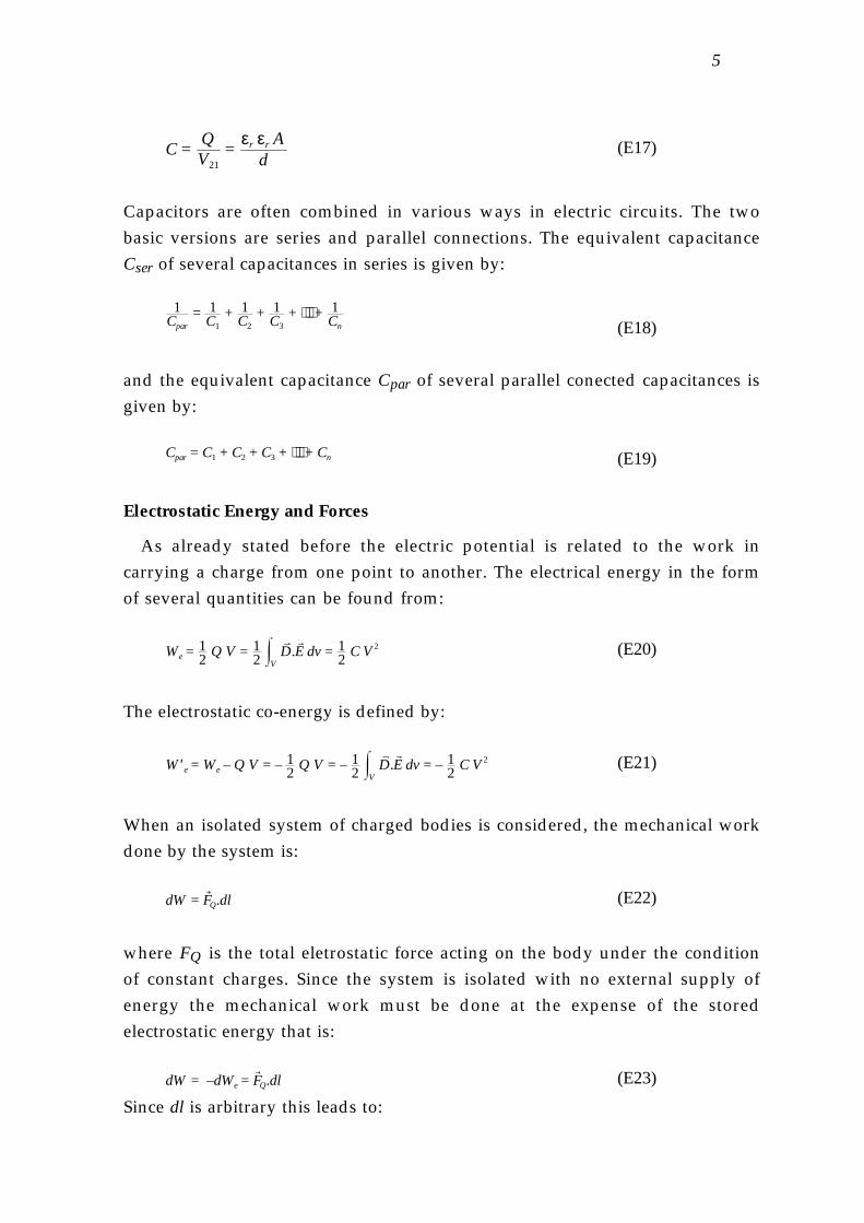
5
C = QV21
= εr εr Ad
(E17)
Capacitors are often combined in various ways in electric circuits. The twobasic versions are series and parallel connections. The equivalent capacitanceCser of several capacitances in series is given by:
1Cpar
= 1C1
+ 1C2
+ 1C3
+ ⋅⋅⋅ + 1Cn (E18)
and the equivalent capacitance Cpar of several parallel conected capacitances isgiven by:
Cpar = C1 + C2 + C3 + ⋅⋅⋅ + Cn (E19)
Electrostatic Energy and Forces
As already stated before the electric potential is related to the work incarrying a charge from one point to another. The electrical energy in the formof several quantities can be found from:
We = 12 Q V = 1
2 D.E dvV
= 12 C V2 (E20)
The electrostatic co-energy is defined by:
W′ e = We – Q V = – 12 Q V = – 1
2 D.E dvV
= – 12 C V2 (E21)
When an isolated system of charged bodies is considered, the mechanical workdone by the system is:
dW = FQ.dl (E22)
where FQ is the total eletrostatic force acting on the body under the conditionof constant charges. Since the system is isolated with no external supply ofenergy the mechanical work must be done at the expense of the storedelectrostatic energy that is:
dW = –dWe = FQ.dl (E23)
Since dl is arbitrary this leads to:

6
FQ = – ∇ We (E24)
In cartesian coordinates the component forces are:
FQ x= – ∂We
∂x
FQ y= – ∂We
∂y
FQ z= – ∂We
∂z (E25 a,b,c)
or in case the system can rotate about an axis the torque TQ can be found fromits derivative to the angle of rotation φ:
TQ = – ∂We
∂φ (E26)
When the conducting bodies are held at a fixed potential through connectionsto external sources a displacement by a conducting body would result in achange in total electrostatic energy and requires the sources to transfer chargesto the conductors in order to keep them at their fixed potentials. The totalenergy supplied by the sources to the system is:
dWsource = V dQ (E27)
The mechanical work done by the system is:
dW = FV.dl (E28)
where Fv is the electric force on the conducting body under the condition ofconstant potential. The charge transfer also changes the the electrostatic energyof the system by an amount:
dWe = 12 V dQ
(E29)
Conservation of energy demands that:
dW + dWe = dWsource (E30)
The electrostatic force under the condition of constant potential now becomes:

7
FV = ∇ We (E31)
which only differs by a sign change from the electrostatic force at constantcharge.
Static or Dynamic eletrostatic fields?
A final question that has to be answerred is when electrostatic fields can beconsidered as quasi-static fields or have to be considered as dynamic fields. Forthe time-harmonic varying electrostatic field, with angular frequency ω, of aparallel plate condensator with circular plates that have a radius R that is largecompared to the plate distance d the following expression can be derived:
E = E0 1 – ω2 ε0 εr µ0 r2
4 (E32)
This electric field is can be approximated by a time dependent quasi-staticelectrostatic field when:
ωR2 c << 1 (E33)
where c is the speed of light in vacuum (3.108 m/s). For example for a radius of1mm a quasi static approach can be used up to frequencies of about 100 Ghz.

254
BIBLIOGRAPHY
S. Bouwstra, P. Kemna, R. Legtenberg, Thermally excited resonating membrane mass flow sensor,Technical Digest Eurosensors '87, Cambridge, UK, September, 1987, pp. 20-21.
S. Bouwstra, R. Legtenberg and Th. J.A. Popma, Silicon-rich LPCVD silicon nitride films formicromechnical structures, Technical Digest Eurosensors II and 4th Sensors and Actuatorssymposium, Enschede, The Netherlands, November 1988, p. 167.
S. Bouwstra, R. Legtenberg, H. A. C. Tilmans and M. Elwenspoek, Resonating microbridge massflow sensor, Technical Digest Transducers '89 and Eurosensors III, Montreux, Switzerland, June1989, pp. 140-141.
S. Bouwstra, P. Kemna and R. Legtenberg, Thermally excited resonating membrane mass flowsensor, Sensors and Actuators, A20, 1989, pp. 213-223.
S. Bouwstra, R. Legtenberg, H. A. C. Tilmans and M. Elwenspoek, Resonating microbridge massflow sensor, Sensors and Actuators, A21- A23, 1990, pp. 332-335.
R. Legtenberg, S. Bouwstra and M. Elwenspoek, Low-temperature glass bonding for sensorapplications using boron oxide thin films, Proc. 2nd Workshop on micromaching, micromechanicsand microsystems (MME '90), Berlin, Germany, November 26-27, 1990, pp. 94-99.
R. Legtenberg, S. Bouwstra and J.H.J. Fluitman, Resonating mass flow sensor with low-temperature bonded cap wafer, Sensors and Actuators , A25-A27, 1991, pp. 723-727.
R. Legtenberg, S. Bouwstra and M. Elwenspoek, Low-temperature glass bonding for sensorapplications using boron oxide thin films, J. Micromech. Microeng., 1, 1991, pp. 157-160.
H. A. C. Tilmans and R. Legtenberg, Electrostatically driven vacuum encapsulated polysiliconresonators, poster presentation Eurosensors VI (Book of Abstracts, p. 353), San Sebastian, Spain,5-7 October, 1992. p. 353.
H. A. C. Tilmans, R. Legtenberg, H. Schurer, D. J. IJntema, M. Elwenspoek and J. H. J. Fluitman,(Electro)mechanical characteristics of electrostatically driven vacuum encapsulated polysiliconresonators, IEEE Trans. Ultrasonics, Ferroelectrics and Frequency Control, Vol. 41, No. 1, January1994. pp. 4-6.
R. Legtenberg and H. A. C. Tilmans, Electrostatically driven vacuum encapsulated polysiliconresonators, Part I: Design and fabrication, Sensors and Actuators, A45, 1994, pp. 57-66.
H. A. C. Tilmans and R. Legtenberg, Electrostatically driven vacuum encapsulated polysiliconresonators, Part II: Theory and performance, Sensors and Actuators, A45, 1994, pp. 67-84.
R. Legtenberg, H. Tilmans, J. Elders and M. Elwenspoek, Stiction of surface micromachinedstructures after rinsing and drying: Model and investigation of adhesion mechanisms, Proc. 7thInt. Conf. Solid State Sensors and Actuators (Transducers '93), Yokohama, Japan, June 7 - 10, 1993,pp. 198-201.
R. Legtenberg, H. Jansen, M. Elwenspoek and J. Fluitman, Micro Joints, Book of abstracts, 13-thBenelux Meeting on Stystems and Control, Veldhoven, The Netherlands, March 2-4, 1994, p. 26.

Bibliography 255
R. Legtenberg, H. Tilmans, J. Elders and M. Elwenspoek, Stiction of surface micromachinedstructures after rinsing and drying: Model and investigation of adhesion mechanisms, Sensors andActuators, A43, 1994, pp. 230-238.
R. Legtenberg, E. Berenschot, M. Elwenspoek and J. Fluitman, Electrostatic curved electrodeactuators, Proc. IEEE Micro Electro Mechanical Systems, Amsterdam, The Netherlands, Jan. 29-Feb. 2, 1995, pp. 37-42.
J.R. Gilbert, R. Legtenberg and S.D. Senturia, 3D coupled electromechanics for MEMS:Applications of CoSolve-EM, Proc. IEEE Micro Electro Mechanical Systems, Amsterdam, theNetherlands, Jan. 29-Feb. 2, 1995, pp. 122-127.
H. Jansen, M. de Boer, R. Legtenberg and M. Elwenspoek, The black silicon method: a universalmethod for determining the parameter setting of a fluorine-based reactive ion etcher in deepsilicon trench etching with profile control, J. Micromechanics and Microengineering, Vol. 5, 1995,pp. 115-120.
H. Jansen, M. de Boer, J. Burger, R. Legtenberg and M. Elwenspoek, The black silicon methodII:The effect of mask material and loading on the reactive ion etching of deep silicon structures,Microelectronic Engineering, Vol. 27, 1995, pp. 475-480.
C. Gui, R. Legtenberg, M. Elwenspoek and J. Fluitman, Q-factor dependance of one-portencapsulated polysilicon resonators on reactive sealing pressure, J. Micromechanics andMicroengineering, Vol. 5, 1995, pp. 183-185.
C. Gui, R. Legtenberg, H. Tilmans, J. Fluitman and M. Elwenspoek, Nonlinearity and hysteresis ofresonant strain gauges, Proc. IEEE Micro Electro Mechanical Systems, Amsterdam, TheNetherlands, Jan. 29-Feb. 2, 1995, pp. 157-162.
R. Legtenberg, H. Jansen, M. de Boer and M. Elwenspoek, Anisotropic reactive ion etching ofsilicon using SF6/O2/CHF3 gas mixtures, J. Electrochem. Soc., Vol. 142, No. 6, June, 1995, pp.2020-2027.
European Patent No. 94202519.8: Process for producing micromechanical structures by means ofreactive ion etching.
R. Legtenberg, E. Berenschot, J. van Baar, Th. Lammerink and M. Elwenspoek, An electrostaticlower stator axial gap wobble motor: design and fabrication, Proc. 8th Int. Conf. Solid StateSensors and Actuators (Transducers '95), Stockholm, Sweden, June 25 - 29, 1995, pp. 404-407.
R. Legtenberg, A.W. Groeneveld and Miko Elwenspoek, Towards position control of electrostaticcomb drives, Proc. Micro Mechanics Europe Workshop, Copenhagen, Denmark, September 3-5,1995, pp. 124-127.
R. Legtenberg, E. Berenschot, M. Elwenspoek and J.H.J. Fluitman, Electrostatic actuators withintegrated gear linkages for mechanical power transmission, Proc. IEEE Micro ElectroMechanical Systems, San Diego, CA, U.S.A., Feb. 11-15, 1996.
R. Legtenberg, E. Berenschot, J. van Baar and M. Elwenspoek, An electrostatic axial gap wobblemotor, submitted to the Journal of Micro Electro Mechanical Systems.
R. Legtenberg, A.W. Groeneveld and M. Elwenspoek, Comb drive actuators for largedisplacements, J. Micromech. Microeng., 6, 1996, pp. 320-329.

256
DANKWOORD (Acknowledgements)
De resultaten zoals beschreven in dit proefschrift zouden niet mogelijk zijngeweest zonder de inbreng van vele personen van zowel binnen als buitenUniversiteit Twente.
Allereerst wil ik mijn promotoren Jan Fluitman en Theo Popma en assistentpromotor Miko Elwenspoek bedanken voor het geven van de mogelijkheidom als HTS'er te promoveren, alsmede voor het in mij gestelde vertrouwenom dit succesvol af te ronden. Het was destijds een moeilijke beslissing ommijn vaste aanstelling als technicus aan de universiteit op te geven en desprong te wagen. Miko wil ik verder bedanken voor de vele discussies die eenbelangrijke bijdrage hebben geleverd aan hoe te opereren als zelfstandigwetenschapper. Voorts wil ik Siebe Bouwstra en Harrie Tilmans bedankenvoor het overdragen van hun expertise op het gebied van micromechanica envele andere zaken, gedurende mijn aanstelling als technicus. Samenwerkenmet jullie was een fijne tijd en heeft een grote rol gespeeld in de ontwikkelingvan mijn kennis en ervaring.
De stichting FOM/STW wordt bedankt voor de financiele ondersteuningvan het project en het aanbieden van diverse cursussen en de sponsoring vandiverse reizen en verblijven in zowel binnen- en buitenland. Naastconferentie bezoeken ben ik ook in de mogelijkheid gesteld om een aantalmaanden aan het Massachusetts Institure of Technology te werken. My stay,during the summer of 1994, at the MEMCAD group of the MicrosystemTechnology Laboratories at the Massachusetts Institute of Technology inBoston, supervised by Steve Senturia, was a very stimulating and pleasantexperience which I will never forget. Steve, thank you for giving me theopportunity to work in your group and arranging the visit to the Hilton Head1994 conference. I also wish to thank John Gilbert, Peter Osterberg and DanSobek for their help and sharing their time with me. It was fun.
De bijdragen van verschillende studenten, in chronologische volgorde: HansSchurer, Geert Langereis, Nico van Dellen, Marc van der Reijden, RemmertWittebrood, John van Baar en Aart-Wichert Groeneveld dienen ook vermeldte worden. Bedankt voor jullie inspanning en inzet.
Vanwege het technologische karakter van het onderzoek heeft de staf van deMESA cleanroom een belangrijke bijdrage aan het werk gehad. Allemaalhartelijk dank voor jullie hulp en ondersteuning. Met name wil ik Arie Kooybedanken voor zijn hulp en inzet bij het ontwerpen en het flitsen van velemaskers. Altijd wist hij maskers met moelijke flitspatronen en dimensies die

Acknowledgements 257
op de grenzen van de mogelijkheden van de patroon generator lagen tevoorschijn te toveren. Verder wil ik Bert Otter in het bijzonder danken voorzijn hulp bij het maken van de AFM scans en de vele SEM foto's.
Veel dank ben ik ook verschuldigd aan Erwin Berenschot. Zijnondersteuning en technologische vaardigheden hebben een belangrijkebijdrage geleverd aan de realisatie van vele devices in dit proefschrift. Verderwil ik Meint de Boer bedanken voor zijn hulp bij het anisotroop ets onderzoeken samen met Henri Jansen voor de vele discussies op het gebied vananisotroop etsen.
Voorts wil ik alle MicMec'ers bedanken voor de samenwerking en deplezierige werksfeer. De vele koffie, taart en bier hebben hier zeker aanbijgedragen. Met name mijn voormalige en huidige kamergenoten; HanGardeniers, Job Elders, Thijs van Toor, Jan-Kees te Riet Scholten, Gui Chenqunen Joost van Kuijk wil ik hierbij noemen.
Ook Dick Ekkelkamp, Judith Beld en Jose Nijhuis-Effing wil ik danken voorhun hulp op administratief en financieel gebied.
Veel dank ben ik verder verschuldigd aan Jan van Schoot en GerloHesselink. In het PC imperium binnen vakgroep TDM heb ik een onmisbarehulp gehad van hen op het gebied van software ondersteuning op mijnMacIntosh.
Han Gardeniers en Marina Maund wil ik hierbij bedanken voor hetaandachtig doorlezen van mijn concept proefschrift en de respectievelijkeinhoudelijke correcties en verbeteringen van de Engelse taal.
Verder dank ik mijn familie en vrienden voor hun interesse, steun enmomenten van ontspanning.
Als laatste maar zeker niet in de minste plaats wil ik Manuela bedankenvoor haar geduld, liefde, zorg en vertrouwen in mij tijdens de afgelopen vierjaren.

258
BIOGRAPHY
Rob Legtenberg was born on June 21, 1964, in Hengelo, The Netherlands. Hereceived a B.Sc. degree in Applied Physics from the Hogere Technische School,Enschede, The Netherlands, in 1985. His graduate project at the University ofTwente, Enschede, The Netherlands, dealt with the fabrication of passive andactive planar optical waveguides by spin- and dip coating.
After fulfilling his military service, he joined the Micromechanical ResearchGroup at the University of Twente as a process engineer in 1986. His workincluded the development of micromachining techniques and fabrication andcharacterisation of micromechanical devices. The main subjects wereresonating microbridge mass flow sensors and vacuum encapsulatedelectrostatically driven polysilicon resonators. Cooperative work on therealisation of resonating force sensors, micropumps, flow sensors and liquiddosing systems was also performed.
In 1992 he started the research on electrostatic actuators fabricated by surfacemicromachining techniques, as described in this thesis, in the same group atthe MESA Research Institute at the University of Twente. During the summerof 1994 he visited the MEMCAD group at the Massachusetts Institute ofTechnology (MIT), supervised by Prof. S. D. Senturia, to work on coupledelectromechanical simulations of curved electrode actuators using theCoSolve-EM system.
Besides his work he enjoys music and piano playing, reading, billiards,fitness, as well as jogging and outdoor activities. Growing bonsai trees, homeimprovement and spending time with friends are also amongst his favouriteactivities.

259
LEVENSLOOP
Rob Legtenberg werd geboren op 21 Juni, 1964, in Hengelo. Na de middelbareschool begon hij in 1981 met de studie Technische Natuurkunde aan deHogere Technische School te Enschede waar hij in 1985 afstudeerde. Zijnafstudeeropdracht had betrekking op de fabricage van passieve en actieveplanaire golfgeleiders door middel van spin- en dip coating.
Na het doorlopen van de militaire diensplicht trad hij in 1986 in dienst vanUniversiteit Twente als proces technoloog binnen de onderzoeksgroepMicromechanische Systemen. Hier werkte hij aan de ontwikkeling van"micromachining" technieken en de fabricage en karakterisatie vanmicromechanische sensoren en actuatoren. Belangrijke onderwerpen warenresonerende mass-flow sensoren en vacuum ingekapselde, electrostatischaangedreven, resonatoren van polykristallijn silicium. Voorts heeft hijbijdragen geleverd aan de realisatie van resonerende kracht sensoren, micropompen, flow sensoren en micro doseer systemen.
In 1992 trad hij als promovendus in dienst van het MESA Research Institutevan de Universiteit Twente en startte het onderzoek naar electrostatischeactuatoren die door middel van "surface micromachining" technieken wordengefabriceerd, zoals beschreven in dit proefschrift. Van juni 1994 tot en metaugustus 1994 werkte hij aan het Massachusetts Institute of Technology (MIT),onder leiding van Prof. S. D. Senturia, aan gekoppelde electromechanischesimulaties van kromme electrode actuatoren met behulp van het CoSolve-EMsysteem.
Naast zijn werk houd hij van muziek, piano spelen, lezen en biljarten. Hijslooft zich regelmatig uit in het fitness centrum, doet wat aan joggen en houdvan kamperen. Verder zijn het kweken van bonsai, klussen in huis en uitgaanmet vrienden favoriete bezigheden van hem.