pdfs.semanticscholar.org · old dominion university odu digital commons physics theses &...
TRANSCRIPT

Old Dominion University Old Dominion University
ODU Digital Commons ODU Digital Commons
Physics Theses & Dissertations Physics
Fall 2019
Characterization of Argon and Ar/ClCharacterization of Argon and Ar/Cl2 Plasmas Used for the Processing 2 Plasmas Used for the Processing
of Niobium Superconducting Radio-Frequency Cavities of Niobium Superconducting Radio-Frequency Cavities
Jeremy J. Peshl
Old Dominion University, [email protected]
Follow this and additional works at: https://digitalcommons.odu.edu/physics_etds
Part of the Atomic, Molecular and Optical Physics Commons, and the Plasma and Beam Physics
Commons
Recommended Citation Recommended Citation Peshl, Jeremy J.. "Characterization of Argon and Ar/Cl2 Plasmas Used for the Processing of Niobium
Superconducting Radio-Frequency Cavities" (2019). Doctor of Philosophy (PhD), Dissertation, Physics, Old Dominion University,
DOI: 10.25777/wykg-dp47
https://digitalcommons.odu.edu/physics_etds/122
This Dissertation is brought to you for free and open access by the Physics at ODU Digital Commons. It has been accepted for inclusion in
Physics Theses & Dissertations by an authorized administrator of ODU Digital Commons. For more information, please contact
CHARACTERIZATION OF ARGON AND Ar/Cl2
PLASMAS USED FOR THE PROCESSING OF NIOBIUM
SUPERCONDUCTING RADIO-FREQUENCY CAVITIES
by
Jeremy J. PeshlB.S. May 2013, Grand Valley State UniversityM.S. Aug 2015, Old Dominion University
A Dissertation Submitted to the Faculty of the Department of PhysicsOld Dominion University in Partial Fulllment of the
Requirements for the Degree of
DOCTOR IN PHILOSOPHY
PHYSICS
OLD DOMINION UNIVERSITYDecember 2019
Approved by:
Leposava Vuskovi¢ (Director)
Gail Dodge (Member)
Alexander L. Godunov (Member)
Gianluigi Ciovati (Member)
Mileta Tomovic (Member)

ABSTRACT
CHARACTERIZATION OF ARGON AND Ar/Cl2 PLASMAS USEDFOR THE PROCESSING OF NIOBIUM SUPERCONDUCTING
RADIO-FREQUENCY CAVITIES
Jeremy J. PeshlOld Dominion University, 2019Director: Dr. Leposava Vuskovi¢
The plasma processing of superconducting radio-frequency (SRF) cavities has
shown signicant promise as a complementary or possible replacement for the cur-
rent wet etch processes. Empirical relationships between the user-controlled external
parameters and the eectiveness of Reactive Ion Etching (RIE) for the removal of
surface layers of bulk niobium have been previously established [1]. However, a lack
of a physical description of the etching discharge, particularly as the external param-
eters are varied, limits the development of this technology. A full understanding of
how these external parameters aect both the amount of material removed and the
physical properties of the plasma would aid researchers in the development of a con-
trollable and customizable cavity processing technique. While the RIE of integrated
circuits on semiconductor wafers has been studied extensively, the unique properties
of the discharge with the application of RIE to a complex 3-D metallic waveguide
make comparisons dicult. Thus, electrical probe and spectroscopy techniques were
applied to a coaxial cylindrical capacitively coupled plasma designed for the plasma
processing of SRF cavities with the intention of nding pertinent relationships be-
tween the external parameters and the important plasma parameters.
A comparative analysis of two popular spectroscopy techniques was conducted in
this aim. The density of the metastable and resonant levels in Ar was measured in
both Ar and Ar/Cl2 discharges to properly characterize the unique discharge system
and aid in the development of a cavity etching routine. The rst method, deemed
the branching fraction method, utilizes the sensitivity of photon reabsorption of
radiative decay to measure the lower state (metastable and resonant) densities by
taking ratios of spectral lines with a common upper level. This method has been
gaining popularity as it does not require any a priori knowledge about the electron
energy distribution. The second method is a tunable diode laser absorption spec-
troscopy technique that measures the thermal Doppler broadening of spectral lines,

from which the neutral gas temperature and lower state density of the transition can
be evaluated. The two methods were conducted in tandem while external param-
eters that were empirically determined to be important to the etching mechanism
of SRF cavities were varied. Relationships between the excited state densities and
the external parameters are presented for both spectroscopy methods. In particular,
the relationship between the rst four excited state densities and the added DC bias
indicate an increase in the plasma density and excited state ionization. The results
found from the spectroscopic studies were applied to a collisional radiative model
(CRM) to determine quantities related to the electron energy distribution. This is
because electrons facilitate the vast majority of the collisional processes in the plasma
bulk, leading to ionization and excitation. Results from the CRM were compared to
Langmuir probe measurements assuming a Maxwellian distribution.
As an extension to the previous empirical investigation, niobium samples were
plasma etched to study the roughness prole of the nal surface as a function of ex-
ternal parameters. In particular, the positive DC bias and surface temperature were
given signicant attention as they are directly related to the physical and chemical
etching mechanisms, respectively. As an unexpected consequence, a great deal of
qualitative information regarding the construction and material limitations of the
reactor were found. The highly reactive Ar/Cl2 gas used for processing can have
detrimental eects to the health of the experimental apparatus, as well as introduce
impurities to the system through reactions with the necessary vacuum chamber and
sealing materials. Suggestions for material improvements to the plasma reactor are
given based on physical observations and surface prole results.

iv
Copyright, 2020, by Jeremy J. Peshl, All Rights Reserved.

v
"I don't do magic, Morty, I do science. One takes brains, the other takes dark
eyeliner."
-Pickle Rick, Rick and Morty

vi
ACKNOWLEDGMENTS
As I come to the end of my graduate school journey, I nd that my success was
dependent on a great deal of people who not only supported me throughout, but
endured the process by my side. I owe many of these people a debt I cannot expect
to repay, but at the very least I would like to express my gratitude. I rst have to
thank my advisor Dr. Vu²kovi¢ for her everlasting encouragement, support, energy,
and most importantly, belief in me. In those moments of my highest doubt in myself
she was always the rst voice of encouragement. Her eorts made me a scientist
rather than just a researcher, and for that I am incredibly grateful. I must of course
also thank my 'pseudo-advisor' Dr. Popovi¢ for all of his help throughout this work.
Not even a brain tumor stopped him from making me a priority in his life, which is
awe-inspiring and only one example of his commitment to science and his students.
I would also like to thank Dr. Sukenik for his continued help and encouragement
throughout this work. I leaned on Dr. Sukenik for a great deal, both experimentally
and personally, and his desire to see students succeed is evident in all of his pursuits.
A special thank you is due for Justin Mason who has allowed me to bother him and
steal his equipment without a second thought. He is also a great friend, and someone
who I admire dearly. Thank you to Ms. Lisa Okun for her support, patience, and
grace in constantly dealing with my equipment orders, problems, travel, and so much
more. Much of the success of this work is also due to the contribution by Roderick
McNeill in his short time working in the lab with me. Besides being a talented
researcher and clever thinker, while he was certainly a source of snide comments, he
was also a constant source of encouragement in moments of doubt and I would not be
here without him. Thanks is also due to Dr. Valente-Feliciano and Dr. Palczewski
for their help with materials and services performed at JLab, and to Olga Tromova
for her patience and help with the surface studies.
I also could not have gotten to this point without the support of my amazing
friends and family throughout the years. Thank you to Robert Fields for being one
of very few sources of encouragement and hope through the rst few years of graduate
school, and for being a great friend to me since the day we met. I must also thank
Torri Jeske, Tyler Viducic, Dr. Grady White, Lindsay Thornton, and Josh Carter for
their friendship and mental support through this experience. It is also important to
include Borjo coeehouse, in which I anticipate I have spent ≈ 5 % of my total gross

vii
salary while being in graduate school. I regret none of it, and their coee fueled this
dissertation. To my friends from Michigan, I don't know how I could be so lucky to
have such an amazing group of people in my life. The support I receive from them
on a daily basis is astonishing, let alone the various visits, trips, DoTA games, phone
calls, and messages that I've received over the years in my most dicult moments.
To Courtney Miller, who lived the struggle with me, thank you for your love and
support for all of those years. Lastly, I must thank my parents Ron and Kathy, and
my brother Darren, for their constant love and support. I could not ask for better
people in my life.
This work is supported by the Oce of High Energy Physics, Oce of Science,
Department of Energy under Grant No. DE-SC0014397.

viii
TABLE OF CONTENTS
Page
LIST OF TABLES . . . . . . . . . . . . . . . . . . . . . . . . . . . . . . . . . . . . . . . . . . . . . . . . . . . . . . . . . . . . x
LIST OF FIGURES . . . . . . . . . . . . . . . . . . . . . . . . . . . . . . . . . . . . . . . . . . . . . . . . . . . . . . . . . . . xi
Chapter
1. INTRODUCTION . . . . . . . . . . . . . . . . . . . . . . . . . . . . . . . . . . . . . . . . . . . . . . . . . . . . . . . . . 1
2. BASICS OF PLASMA DISCHARGES . . . . . . . . . . . . . . . . . . . . . . . . . . . . . . . . . . . . . 62.1 THE QUASINEUTRALITY CONDITION . . . . . . . . . . . . . . . . . . . . . . . . 72.2 PLASMA SOURCES . . . . . . . . . . . . . . . . . . . . . . . . . . . . . . . . . . . . . . . . . . 92.3 PLASMA PARAMETERS AND CHARACTERISTICS . . . . . . . . . . . . 13
3. SRF CAVITY ACCELERATORS . . . . . . . . . . . . . . . . . . . . . . . . . . . . . . . . . . . . . . . . . . 183.1 CAVITY PERFORMANCE FIGURES OF MERIT . . . . . . . . . . . . . . . . 203.2 SUPERCONDUCTIVITY . . . . . . . . . . . . . . . . . . . . . . . . . . . . . . . . . . . . . . 233.3 LOSSES IN SRF CAVITIES . . . . . . . . . . . . . . . . . . . . . . . . . . . . . . . . . . . . 263.4 CAVITY PROCESSING . . . . . . . . . . . . . . . . . . . . . . . . . . . . . . . . . . . . . . . 28
4. PLASMA PROCESSING AND ITS APPLICATION TO SRF CAVITIES . . 314.1 THE Nb RING SAMPLE EXPERIMENT . . . . . . . . . . . . . . . . . . . . . . . . 314.2 DRIVEN ELECTRODE GEOMETRY AND THE MODIFICATION
OF THE PLASMA ASYMMETRY . . . . . . . . . . . . . . . . . . . . . . . . . . . . . . 394.3 CRYOGENIC RF TEST OF THE FIRST SRF CAVITY ETCHED
WITH AN Ar/Cl2 PLASMA . . . . . . . . . . . . . . . . . . . . . . . . . . . . . . . . . . . . 45
5. PLASMA DIAGNOSTIC METHODS . . . . . . . . . . . . . . . . . . . . . . . . . . . . . . . . . . . . . . 485.1 LANGMUIR PROBES . . . . . . . . . . . . . . . . . . . . . . . . . . . . . . . . . . . . . . . . . 485.2 OPTICAL EMISSION SPECTROSCOPY . . . . . . . . . . . . . . . . . . . . . . . . 535.3 COLLISIONAL RADIATIVE MODEL . . . . . . . . . . . . . . . . . . . . . . . . . . . 655.4 TUNABLE DIODE LASER ABSORPTION SPECTROSCOPY . . . . . 71
6. EXPERIMENTAL SETUP. . . . . . . . . . . . . . . . . . . . . . . . . . . . . . . . . . . . . . . . . . . . . . . . . 766.1 MODULAR DISCHARGE REACTOR . . . . . . . . . . . . . . . . . . . . . . . . . . . 766.2 OPTICAL EMISSION SPECTROSCOPY . . . . . . . . . . . . . . . . . . . . . . . . 836.3 TUNABLE DIODE LASER. . . . . . . . . . . . . . . . . . . . . . . . . . . . . . . . . . . . . 896.4 LANGMUIR PROBE . . . . . . . . . . . . . . . . . . . . . . . . . . . . . . . . . . . . . . . . . . 976.5 Nb SAMPLE SURFACE ROUGHNESS EXPERIMENT . . . . . . . . . . . . 101

ix
7. DENSITIES OF ARGON EXCITED STATES VS. EXTERNAL PLASMAPARAMETERS. . . . . . . . . . . . . . . . . . . . . . . . . . . . . . . . . . . . . . . . . . . . . . . . . . . . . . . . . . . . 1067.1 TDLAS VS. OES-BFM . . . . . . . . . . . . . . . . . . . . . . . . . . . . . . . . . . . . . . . . . 1077.2 LIMITATIONS OF OES-BFM . . . . . . . . . . . . . . . . . . . . . . . . . . . . . . . . . . 1087.3 GAS TEMPERATURE . . . . . . . . . . . . . . . . . . . . . . . . . . . . . . . . . . . . . . . . 1097.4 RESULTS AND DISCUSSION . . . . . . . . . . . . . . . . . . . . . . . . . . . . . . . . . . 111
8. EFFECTS OF EXTERNAL PARAMETERS ON THE ELECTRON DIS-TRIBUTION. . . . . . . . . . . . . . . . . . . . . . . . . . . . . . . . . . . . . . . . . . . . . . . . . . . . . . . . . . . . . . . 1248.1 Te AND ne MEASUREMENT AND CALCULATION SOURCES . . . . 1248.2 LANGMUIR PROBE RESULTS . . . . . . . . . . . . . . . . . . . . . . . . . . . . . . . . 1258.3 CRM RESULTS AND SELF-CONSISTENCY . . . . . . . . . . . . . . . . . . . . . 1278.4 THE ELECTRON TEMPERATURE AND DENSITY AS A FUNC-
TION OF EXTERNAL PARAMETERS . . . . . . . . . . . . . . . . . . . . . . . . . . 1288.5 THE CALCULATION OF ne USING THE COMBINATION METH-
ODS . . . . . . . . . . . . . . . . . . . . . . . . . . . . . . . . . . . . . . . . . . . . . . . . . . . . . . . . . 1328.6 Ar/Cl2 RESULTS . . . . . . . . . . . . . . . . . . . . . . . . . . . . . . . . . . . . . . . . . . . . . 1368.7 GENERAL CONCLUSIONS . . . . . . . . . . . . . . . . . . . . . . . . . . . . . . . . . . . . 1398.8 COMPARISONS TO TRADITIONAL REACTORS AND CONNEC-
TIONS TO REACTIVE ION ETCHING . . . . . . . . . . . . . . . . . . . . . . . . . 140
9. SURFACE CHARACTERISTICS OF PLASMA ETCHED Nb SAMPLES . . 1429.1 THE Nb COUPON ETCHING EXPERIMENT . . . . . . . . . . . . . . . . . . . 1439.2 SAMPLE ETCH RATE . . . . . . . . . . . . . . . . . . . . . . . . . . . . . . . . . . . . . . . . 1439.3 SURFACE MEASUREMENT SYSTEMS . . . . . . . . . . . . . . . . . . . . . . . . . 1489.4 SUMMARY . . . . . . . . . . . . . . . . . . . . . . . . . . . . . . . . . . . . . . . . . . . . . . . . . . 158
10. CONCLUSION . . . . . . . . . . . . . . . . . . . . . . . . . . . . . . . . . . . . . . . . . . . . . . . . . . . . . . . . . . . . 160
REFERENCES. . . . . . . . . . . . . . . . . . . . . . . . . . . . . . . . . . . . . . . . . . . . . . . . . . . . . . . . . . . . . . . . 164
VITA. . . . . . . . . . . . . . . . . . . . . . . . . . . . . . . . . . . . . . . . . . . . . . . . . . . . . . . . . . . . . . . . . . . . . . . . . . 175

x
LIST OF TABLES
Table Page
1 Short list of common superconducting materials and their respective crit-ical temperatures. . . . . . . . . . . . . . . . . . . . . . . . . . . . . . . . . . . . . . . . . . . . . . . . . 23
2 The rst fourteen levels of excited Argon. Levels are labeled in Paschennotation. . . . . . . . . . . . . . . . . . . . . . . . . . . . . . . . . . . . . . . . . . . . . . . . . . . . . . . . . 55
3 The Einstein coecient and branching fraction for the optically allowed2p → 1s transitions [56]. . . . . . . . . . . . . . . . . . . . . . . . . . . . . . . . . . . . . . . . . . . . 58
4 The rate constants Q0 and tting parameter b used in this work. Valuestaken from Refs. [68, 69]. . . . . . . . . . . . . . . . . . . . . . . . . . . . . . . . . . . . . . . . . . . 69
5 The external parameters studied. The * indicates that these values arenot present for all data sets due to experimental limitations. . . . . . . . . . . . . 107
6 The parameter combinations for calculating ne using Eq. (83). NR refersto the ratio of 1s5/1s4. The LP results can only be used for dischargeconditions without added DC bias. . . . . . . . . . . . . . . . . . . . . . . . . . . . . . . . . . . 125
7 Results from the CRM for a pure Argon discharge at 50 mTorr, 150 W,and with no added DC bias. . . . . . . . . . . . . . . . . . . . . . . . . . . . . . . . . . . . . . . . 128
8 Summary of the Nb coupon sample experiments. The identier is used forreference in the text and gures. In each case, the discharge conditionsare 150 W, 75 mTorr, and 85/15 % Ar/Cl2. For T1-T5 the total DC biasis 100 V. . . . . . . . . . . . . . . . . . . . . . . . . . . . . . . . . . . . . . . . . . . . . . . . . . . . . . . . . 144
9 RMS results for each sample and experimental conguration. In all cases,the scan area was 50 µm × 50 µm. There were two polished and unetchedsamples with RMS roughness < 30 nm. . . . . . . . . . . . . . . . . . . . . . . . . . . . . . . 152
10 Gasket material and gas feed conguration for each sample experiment. . . 155

xi
LIST OF FIGURES
Figure Page
1 A simple drawing of the voltage distribution in a symmetric discharge(left) and an asymmetric discharge (right). . . . . . . . . . . . . . . . . . . . . . . . . . . . 10
2 Illustration of the plasma asymmetry reversal in a coaxial CCP. Left: Theelectric potential distribution of a normal asymmetric discharge. Right:The electric potential distribution with the asymmetry reversed. Regionsa, b, and c indicate the cavity sheath, the bulk plasma, and the poweredelectrode sheath, respectively. . . . . . . . . . . . . . . . . . . . . . . . . . . . . . . . . . . . . . . 12
3 Example of dierent EEDF forms found in the literature. Each EEDF isplotted with Te = 3 eV. . . . . . . . . . . . . . . . . . . . . . . . . . . . . . . . . . . . . . . . . . . . 16
4 Geometry of an SRF cavity commonly used in particle accelerators today[22]. . . . . . . . . . . . . . . . . . . . . . . . . . . . . . . . . . . . . . . . . . . . . . . . . . . . . . . . . . . . . 19
5 A 1.3 GHz 9-cell SRF cavity developed by the TESLA collaboration in2000 [24]. This design is still widely used in accelerator facilities aroundthe world. . . . . . . . . . . . . . . . . . . . . . . . . . . . . . . . . . . . . . . . . . . . . . . . . . . . . . . . 20
6 Scheme of the acceleration of a particle through SRF cavities. The par-ticle enters the rst cavity at T = 0 and exits at T = π
ω0to receive the
maximum accelerating eld (black curve). As the particle exits the rstresonator and enters the second, the time varying eld has changed sign(red curve) and the process is repeated. It is for this reason there is anodd number of resonators in accelerating cavities (Figure 5). . . . . . . . . . . . 22
7 Photos of the niobium ring samples with a width of 2.5 cm and diameterof 7.2 cm. The diameter is comparable to the diameter of an SRF cavitybeamtube. (a) Top view (b) Side view [36]. . . . . . . . . . . . . . . . . . . . . . . . . . . 32
8 Etch rate dependence on the combination of DC bias and gas composition.Conditions were as follows: RF power = 150 W, pressure = 150 mTorr,electrode diameter = 5.08 cm, chamber temperature = 422 K [7]. . . . . . . . 33
9 Left: Etch rate of ring sample vs. DC bias. Right: Etch rate ratio oftwo ring samples vs. DC bias. Conditions were as follows: RF power =150 W, pressure = 150 mTorr, electrode diameter = 5.08 cm, chambertemperature = 422 K, gas composition = 85/15 % Ar/Cl2 [7]. . . . . . . . . . . 34

xii
10 Left: Etch rate of ring sample vs. Cl2 concentration [36]. Right: Etchrate ratio of two ring samples vs. Cl2 concentration [7]. Conditions wereas follows: RF power = 150 W, pressure = 150 mTorr, electrode diameter= 5.08 cm, chamber temperature = 422 K, positive DC bias = 290 V. . . . 36
11 Left: Etch rate of ring sample vs. substrate temperature. Right: Etchrate ratio of two ring samples vs. surface temperature. Conditions wereas follows: RF power = 150 W, pressure = 150 mTorr, electrode diameter= 5.08 cm, positive DC bias = 290 V, gas composition = 85/15 % Ar/Cl2[7]. . . . . . . . . . . . . . . . . . . . . . . . . . . . . . . . . . . . . . . . . . . . . . . . . . . . . . . . . . . . . . 37
12 Left: Etch rate of ring sample vs. RF power. Right: Etch rate ratio oftwo ring samples vs. RF power. Conditions were as follows: pressure =150 mTorr, electrode diameter = 5.08 cm, chamber temperature = 422K, positive DC bias = 290 V, gas composition = 85/15 % Ar/Cl2 [7]. . . . . 38
13 Left: Etch rate of ring sample vs. pressure. Right: Etch rate ratio of tworing samples vs. pressure. Conditions were as follows: RF power = 150W, electrode diameter = 5.08 cm, chamber temperature = 422 K, positiveDC bias = 290 V, gas composition = 85/15 % Ar/Cl2 [7]. . . . . . . . . . . . . . . 39
14 Illustration of various structures used for the study of the modicationof plasma asymmetry, listed in increasing order of surface area [8]. (a)5.0 cm diameter smooth straight tube, (b) large pitch bellows with 3.8cm inner diameter and 4.8 cm outer diameter, (c) Disk-loaded corrugatedstructure with 5.0 cm outer diameter and 2.5 cm inner diameter. Eachdisk is 1.0 mm thick and separated by 3.0 mm. . . . . . . . . . . . . . . . . . . . . . . . 41
15 Left: Self-bias voltage vs. RF power in a pure Argon discharge. The self-bias voltage is negative for each geometry, but is presented as positive forclarity. Right: Self-bias vs. RF power in an Ar/Cl2 (85/15 %) discharge[8]. The pressure is 450 mTorr in both cases. . . . . . . . . . . . . . . . . . . . . . . . . . 42
16 DC Current vs. RF power for dierent electrode geometries in both Arand Ar/Cl2 discharges [8]. The pressure is 450 mTorr in both cases. . . . . . 43
17 Nb etch rate vs. electrode geometry [8]. The discharge conditions were asfollows: RF power = 150 W, Pressure = 60 mTorr, VDC = 290 V, SurfaceTemperature = 422 K. . . . . . . . . . . . . . . . . . . . . . . . . . . . . . . . . . . . . . . . . . . . . 44
18 (a) Schematic diagram of the experimental setup of the single cell cavityetching system. (b) Photo of the cavity etching system. The direction ofthe electrode and gas feed movement are highlighted [38]. . . . . . . . . . . . . . . 45
19 The rf performance test results of the plasma etched SRF cavity at 1.8 K[38]. The quality factor Q0 and eld emission are presented in tandem. . . 46

xiii
20 The surface analysis (left) and elemental composition (right) of the residueon the surface of the cavity after plasma etching [38]. . . . . . . . . . . . . . . . . . . 47
21 A theoretical I-V characteristic. This gure follows the common practiceof plotting the characteristic with the electron current as positive and theion current as negative. . . . . . . . . . . . . . . . . . . . . . . . . . . . . . . . . . . . . . . . . . . . . 50
22 A semilog plot of the I-V characteristic. The electron temperature can befound by tting the linear region and calculating the slope. . . . . . . . . . . . . . 52
23 The possible 2p → 1s transitions for Argon [11]. . . . . . . . . . . . . . . . . . . . . . . 56
24 Resonant radiation reabsorption, or radiation trapping. Level b is opti-cally coupled to the lower level a, while c and d are not. Photons emittedin the b-a transition can re-excite atoms back to level b, allowing for theradiation decay to levels c or d. . . . . . . . . . . . . . . . . . . . . . . . . . . . . . . . . . . . . . 59
25 Various forms of the photon escape factor as a function of optical thicknessfound in literature. Solid black line: [62], Red dashed line: [67], Bluedashed line: Eq. 63, Green dash-dot line: Eq. 65. . . . . . . . . . . . . . . . . . . . . . 64
26 Depiction of a Doppler broadened spectral line/absorption prole. In thereference frame of the observer, fast moving atoms emit/absorb photonsat a frequency shifted o resonance (ν0) based on their velocity. Moredetails can be found in the text. . . . . . . . . . . . . . . . . . . . . . . . . . . . . . . . . . . . . 72
27 A basic 1-D model of absorption in a Doppler broadened medium drawn inthe reference frame of the observer (same frame as the stationary atom).Atoms A, B, and C will all accept the incoming photon and be excited.This is because in the reference frames of each individual atom, the fre-quency of incoming light is equal to ν0, the resonant frequency of thetransition. More details can be found in the text. . . . . . . . . . . . . . . . . . . . . . 73
28 The active plasma discharge chamber. . . . . . . . . . . . . . . . . . . . . . . . . . . . . . . . 77
29 A wire diagram showing dierent perspectives of the coaxial electrode setup. 78
30 Schematic of atmospheric pressure power feedthrough system [1]. . . . . . . . 79
31 Left: A 3-D split-axis depiction of the coaxial electrode region of theapparatus. Right: An end-on view of the coaxial setup. The corrugatedpowered electrode is shown in red and the optical viewports used fordiagnostic methods are in black. . . . . . . . . . . . . . . . . . . . . . . . . . . . . . . . . . . . . 80

xiv
32 Top: The power feed (red) and gas delivery inlet (green) for a pill-boxtype cavity experiment found in the work of Ref. [1]. Bottom: A closeup depiction of the conical gas inlet. . . . . . . . . . . . . . . . . . . . . . . . . . . . . . . . . 81
33 A multi-view depiction of the laminar showerhead. More informationabout the design and eectiveness can be found in Chapter 9. . . . . . . . . . . 82
34 Schematic of the laminar showerhead. All dimensions are shown in inches. 83
35 The 3-D printed ber optic aperture. The piece ts over a DN16 conatange and holds the ber optic in the center. The smaller cylinder issolid plastic with a small hole where the ber is mounted. This eectivelydecreased the acceptance angle of the ber to ≈ 5o. . . . . . . . . . . . . . . . . . . . 84
36 Irradiance as a function of wavelength for the Newport/Oriel TungstenHalogen blackbody source as given by Eq. (93). . . . . . . . . . . . . . . . . . . . . . . 86
37 Intensity as a function of wavelength for the blackbody source as measuredby the OceanOptics ber optic spectroscopy system. . . . . . . . . . . . . . . . . . . 87
38 Example spectral irradiance of an Argon plasma using the OceanOpticssystem. Spectral lines pertinent to the OES methods outlined in Chapter5 are emphasized. The limitations of the spectrometer can be seen assome lines are not distinct and may overlap. . . . . . . . . . . . . . . . . . . . . . . . . . . 88
39 The feed forward circuit schematic. The second stage on the right is aunity gain low pass lter that is only necessary if the signal needs to beinverted. . . . . . . . . . . . . . . . . . . . . . . . . . . . . . . . . . . . . . . . . . . . . . . . . . . . . . . . . 90
40 The experimental TDLAS setup (without the FPI systems). . . . . . . . . . . . . 91
41 Schematic of the TDLAS tabletop setup. . . . . . . . . . . . . . . . . . . . . . . . . . . . . 92
42 Top: The laser path through the plasma chamber. The laser exits the berlauncher on the right and passes through a non-polarizing beamsplittercube before entering the discharge through the viewport. The laser (minusabsorption) exits the chamber and is collected by the photodiode on theleft. Bottom: A cartoon schematic of the discharge and location of thediagnostic tools. While the laser can only travel unobstructed throughviewport A, the ber optic can be placed at A, B, or C. However, locationA was strictly used for both methods to ensure a more direct comparisonof results. . . . . . . . . . . . . . . . . . . . . . . . . . . . . . . . . . . . . . . . . . . . . . . . . . . . . . . . . 93
43 Example of laser absorption measurement using TDLAS: a) Laser absorp-tion and two Fabry-Pérot Interferometer signals (the piezo voltage signalis not pictured); b) The processed signal along with residual plot. . . . . . . . 94

xv
44 Top: The raw home-built etalon signal and the processed signal. Bottom:The time-varying phase cosine function t to the smoothed data. . . . . . . . 95
45 The ThorLabs etalon and nal t for the Home-Built etalon. One can seethat there are 4.95 wavelengths between the two sharp peaks. . . . . . . . . . . 97
46 The Langmuir probe housing and linear translation stage. . . . . . . . . . . . . . . 98
47 An end-on photo of the plasma reactor with the Langmuir probe inserted.A sample for the surface roughness characterization experiment can beseen mounted in the viewport opposite the probe (red arrow). . . . . . . . . . . 99
48 Example of I-V characteristics for dierent current ranges allowed by thesoftware. A close up of two of the scans in the region in which they startto deviate is shown in the upper left corner. . . . . . . . . . . . . . . . . . . . . . . . . . . 100
49 A picture of a Nb coupon sample polished to 1 micron surface roughness.A mirror-like surface can be seen, along with surface defects like pits andtrenches. . . . . . . . . . . . . . . . . . . . . . . . . . . . . . . . . . . . . . . . . . . . . . . . . . . . . . . . . 102
50 The sample mounting and thermocouple setup. The sample is suspendedush to the chamber wall by the threaded rod. The thermocouple is wiredalong the rod and compression t against the back of the sample. . . . . . . . 103
51 The sample mounting locations. Sample 1 is located at the `rear' of theelectrode. Samples 2 and 4 are located at the center of the corrugatedelectrode on opposite sides, and sample 3 is located at the front of theelectrode. The chamber orientation was such that sample 2 is the top ofthe chamber and sample 4 is the bottom. . . . . . . . . . . . . . . . . . . . . . . . . . . . . 105
52 Calculated photon escape factors using Eq. (63) as a function of Ar 1spopulation density. . . . . . . . . . . . . . . . . . . . . . . . . . . . . . . . . . . . . . . . . . . . . . . . 110
53 Density of Ar 1s4 and 1s5 states vs. pressure at 150 W and with no addedbias. Solid lines are visual guidelines. . . . . . . . . . . . . . . . . . . . . . . . . . . . . . . . . 112
54 Ar 1s5 density measured by TDLAS vs. pressure for dierent concentra-tions of Cl2 in Ar with no added bias. Solid lines are visual guidelines. . . . 113
55 Density of Ar a) 1s4 and b) 1s5 densities vs. RF power measured withTDLAS and OES-BFM at 50 mTorr with no added bias. Solid lines arevisual guidelines. . . . . . . . . . . . . . . . . . . . . . . . . . . . . . . . . . . . . . . . . . . . . . . . . . 115
56 Ar 1s5 density measured by TDLAS vs. RF power for dierent concen-trations of Cl2 in an Ar/Cl2 discharge at 50 mTorr with no added bias.Solid lines are visual guidelines. . . . . . . . . . . . . . . . . . . . . . . . . . . . . . . . . . . . . 116

xvi
57 Ar 1s5 density vs. DC bias for 25, 75, 150 W power measured with TDLASand OES-BFM. The dashed lines indicate the negative bias region outlinedin Section 7.4.3. . . . . . . . . . . . . . . . . . . . . . . . . . . . . . . . . . . . . . . . . . . . . . . . . . . 118
58 Ar 1s5 density measured by TDLAS vs. DC bias for 15% Cl2 in an Ar/Cl2discharge. The dashed lines indicate the negative bias region outlined inSec. 7.4.3. Solid/dashed lines are visual guidelines. . . . . . . . . . . . . . . . . . . . . 120
59 Ar 1s5 density measured by TDLAS vs. Cl2 concentration at 75 W. Solidlines are visual guidelines. . . . . . . . . . . . . . . . . . . . . . . . . . . . . . . . . . . . . . . . . . 121
60 Example of a typical I-V characteristic and the Ln(I)-V curve for measur-ing Te. The slope corresponds to a value of Te ≈ 1.2 eV. The pure Argondischarge conditions were 75 mTorr, 100 W, and no added bias. . . . . . . . . . 126
61 Te (left axis) and Vp (right axis) as measured from the Langmuir Probe.The results from the CRM for similar discharge conditions are includedfor comparison. . . . . . . . . . . . . . . . . . . . . . . . . . . . . . . . . . . . . . . . . . . . . . . . . . . . 127
62 Electron Temperature (Left) and Density (Right) vs. RF power. SolidLines are visual guidelines. . . . . . . . . . . . . . . . . . . . . . . . . . . . . . . . . . . . . . . . . . 129
63 Electron Temperature and Density vs. DC bias for 25 W, 75 W and 150W. . . . . . . . . . . . . . . . . . . . . . . . . . . . . . . . . . . . . . . . . . . . . . . . . . . . . . . . . . . . . . 130
64 Te and ne vs. Pressure for discharges without added DC bias. Solid linesare visual guidelines. . . . . . . . . . . . . . . . . . . . . . . . . . . . . . . . . . . . . . . . . . . . . . . 132
65 ne vs. RF power at 50 mTorr for each DC bias conguration. Solid linesare visual guidelines. . . . . . . . . . . . . . . . . . . . . . . . . . . . . . . . . . . . . . . . . . . . . . . 133
66 ne vs. RF power for a pressure of 75 mTorr in each DC bias conguration.Solid lines are visual guidelines. . . . . . . . . . . . . . . . . . . . . . . . . . . . . . . . . . . . . 134
67 ne vs. DC bias for each RF power with discharge pressures 50 and 75mTorr. The dashed lines indicate the negative bias region outlined inSection 7.4.3. . . . . . . . . . . . . . . . . . . . . . . . . . . . . . . . . . . . . . . . . . . . . . . . . . . . . 135
68 ne vs. DC bias for dierent discharge pressures. All data was calculatedusing the TDLAS/CRM NR/Te combination. . . . . . . . . . . . . . . . . . . . . . . . . . 136
69 Te and ne vs. RF power for pure Argon (solid symbols) and Ar/Cl2 (90/10%) for each DC bias conguration at 75 mTorr. Te was found using theCRM, while ne was found using the TDLAS/CRM combination method.Lines are visual guidelines. . . . . . . . . . . . . . . . . . . . . . . . . . . . . . . . . . . . . . . . . . 138

xvii
70 The etch rate vs. temperature for each sample position. Each congura-tion is further labeled by their respective identier from Table 8. . . . . . . . . 145
71 Etch rate vs. 1/kBT and corresponding Arrhenius function t for eachsample as labeled in the top of each pane. . . . . . . . . . . . . . . . . . . . . . . . . . . . . 146
72 Example of a sample after plasma etching. The color indicates chlorinecontaminants on the surface. . . . . . . . . . . . . . . . . . . . . . . . . . . . . . . . . . . . . . . . 147
73 3D AFM images of Nb samples. Left: Polished (1 micron) unetchedsample. Right: Etched sample from experiment T4 in location S3. Thesample location description can be found in Figure 51. . . . . . . . . . . . . . . . . . 149
74 Comparison of surface roughness proles for S4 in each experimental con-guration. Sample location description can be found in Figure 51. . . . . . . . 149
75 AFM scan of S1 in conguration B2. This sample was found to havea negligible etch rate. The sample location description can be found inFigure 51. . . . . . . . . . . . . . . . . . . . . . . . . . . . . . . . . . . . . . . . . . . . . . . . . . . . . . . . 150
76 RMS surface roughness vs. surface temperature for each sample position.The raw data and identier can be found in Table 9. Data is presentedwithout error bars for clarity. . . . . . . . . . . . . . . . . . . . . . . . . . . . . . . . . . . . . . . . 151
77 Material spectrum, spot image, and composition table for sample 1 inthe T1 experimental conguration. The location corresponding to thematerial spectrum is circled in blue. Conguration information can befound in Table 9 and sample location description can be found in Figure51. . . . . . . . . . . . . . . . . . . . . . . . . . . . . . . . . . . . . . . . . . . . . . . . . . . . . . . . . . . . . . 154
78 Left: Example of a location with high carbon deposit (C: 38.83%). Right:Example of a location with high stainless steel impurity deposits (Ni:59.06 % Cr: 2.13 % Fe: 0.92 %). . . . . . . . . . . . . . . . . . . . . . . . . . . . . . . . . . . . . 156
79 Left: Example of a region scan with high Nb concentration (Nb: 71.94 %O: 24.06 %). Right: Example of a region scan with high O concentration(O: 62.14 % Nb: 35.08 %). . . . . . . . . . . . . . . . . . . . . . . . . . . . . . . . . . . . . . . . . . 157

1
CHAPTER 1
INTRODUCTION
The development and use of particle accelerator systems are highly instrumental
in the discovery and understanding of the fundamental particles. It should not be
surprising then that an immense amount of attention is placed on the construction,
development, and advancement of particle accelerator technology. In particular, Su-
perconducting Radio Frequency (SRF) cavity technology is a popular choice in many
laboratories. Particles are accelerated in SRF cavities when high frequency electro-
magnetic elds are produced within the cavities, commonly made from bulk niobium
(Nb). Since these cavities must be superconducting, a great deal of attention must
be given to their construction and maintenance. Barring the consideration of doping
eects or thin lm deposition, the cavities must be of pure grade Nb with mini-
mal impurities and deformities on the SRF cavity surface. These cavities have been
successfully engineered to accelerate particles to velocities near the speed of light,
but the required shape of the cavity is a complicated elliptical structure. To create a
SRF cavity in the desired resonant shape, pieces of bulk niobium must be welded and
formed by tools and machinery that introduce impurities and surface discontinuities.
The resulting impurities, defects, pits, and surface discontinuities from the manufac-
turing and handling of the cavities have detrimental eects on the superconducting
properties, so it should be no surprise that their elimination is extremely important.
Various solutions regarding the surface processing of these cavities have been
developed to specically address surface purity, smoothness, and cleanliness. The
most common processing practices include Buer Chemical Processing (BCP), Elec-
tro Polishing (EP), and Centrifugal Barrel Polishing (CBP). These processes have
proven successful in attaining acceptable superconducting properties in SRF cavi-
ties, but they are not without their issues and limitations. One issue regarding these
processes is personnel and environmental safety as these processes require the use
of dangerous and corrosive chemicals such as hydrouoric acid (HF), sulfuric acid
(H2SO4), and phosphoric acid (H3PO4). Great care must be taken when using and
disposing of these chemicals, and the safety procedures put in place must be quite
rigorous. Scientically, these wet chemical processes do not allow for a great deal of

2
control over the nal surface of the SRF cavity. While machines and routines can be
developed for ecient processing of these cavities, each SRF cavity will have unique
surface properties that cannot be fully addressed using the wet etch processes.
An alternative method for SRF cavity processing is in development and has shown
encouraging results to replace or complement these chemical processes. This ap-
proach, called Reactive Ion Etching (RIE) or sometimes Ion Assisted Reactive Ion
Etching (IARIE), is a technology developed primarily for the semiconductor industry
in the fabrication of integrated circuit products.1 IARIE is a dry etch process that
uses a reactive plasma to facilitate chemical reactions on a material surface. This
is done by introducing a reactive gas, usually a halogen gas or a halogen/inert gas
mixture, to an electromagnetic eld inside a vacuum chamber. This is typically done
by placing the substrate on one of two parallel plates and applying a strong radio-
frequency (RF) electromagnetic eld between the two plates. The ions created from
the heating of the gas are accelerated into the substrate with high enough energy
to react. This is advantageous as the substrate remains close to room temperature,
while the same processes if done chemically would require the substrate to be heated
to very high temperatures. Additionally, IARIE allows for a great deal of control
in the removal of material surface layers as the process can be chemically selective,
removing the desired material and leaving other materials unaected [2]. IARIE can
also be done isotropically where the plasma etches the material without discretion,
or anisotropically where the plasma only etches material in a specic location of the
material [2].
This makes IARIE an intriguing avenue for SRF cavity processing, but natu-
rally implementation of IARIE to SRF cavities is not without its challenges. In the
semiconductor industry the desired amount of surface material removal is on the nm
scale, whereas for SRF cavities removal on the order of microns is desired. The dier-
ence in materials is signicant as well, with polysilicon and Nb having very dierent
surface and material properties. In addition, the semiconductor industry works on
at samples called wafers which are essentially 2D at surfaces. Conversely, SRF
cavities are 3D cylinders with a varying elliptical geometry. Therefore, in order to
extend plasma etching technology into SRF cavity processing, a creative solution is
required to overcome this geometrical challenge.
1Reactive Ion Etching processes are also typically referred to as plasma etching. For all intentsand purposes of this dissertation, these terms are equivalent.

3
Previous studies have made signicant progress in the application of reactive ion
etching to bulk Nb and SRF cavity structures [1]. The vast majority of that work was
done to establish an eective etching apparatus and investigate the relationship be-
tween the user controlled external parameters (such as pressure, temperature, power
sources, and experiment construction) and the rate/amount of material removal. The
experimental apparatus was explicitly constructed to be modular and geometrically
modiable to approximate SRF cavity structures. This allows for the establishment
of the empirical relationships between external parameters and etching on Nb sam-
ples rather than full SRF cavities. While this setup is experimentally and nancially
advantageous, the vacuum components are made out of various materials that can
chemically react or be etched and create a dirty processing environment. The miti-
gation of these unwanted reactions and subsequent impurities remains a signicant
limitation of the technology.
A signicant goal of this work is to continue the development of this method by
establishing relationships between these same external parameters and the gures of
merit that describe an RIE plasma discharge2. In order to create an eective, con-
sistent, and controllable process, knowledge about how the reactive plasma changes
with the etching parameters is imperative. These plasma parameters consist of in-
formation that describe the physical processes and energy distribution in the etching
discharge. The plasma parameters can then be used as inputs for computational
models that can fully describe the plasma reactor. This model would aid in the
development of customizable etching routines and increase the eectiveness of the
etching process while avoiding the need for extensive trial and error experimentation.
There are a great deal of plasma parameters of importance, but information
about the kinetic processes of the electrons within the plasma have signicant value.
Electrons are the most mobile and energetic species in the discharge due to their
low mass compared to the various atomic species in the plasma. For this reason,
electrons are primarily responsible for ionization and excitation of the atomic species,
which is of the utmost importance to surface processing. The measurement and
understanding of these plasma parameters are particularly important because of the
unique geometry and application. In order to etch the inner surface of an SRF cavity,
the plasma must be created within the cavity, meaning that a powered electrode must
2Throughout this dissertation the terms plasma and discharge/ gas discharge are usedinterchangeably. This is commonplace in the eld, particularly in regards to low temperatureplasmas, where the two terms mean essentially the same thing (a partially ionized gas).

4
be placed in the center. This type of conguration creates a coaxial plasma instead
of a at parallel plate plasma commonly used in industrial applications. This oers
the opportunity to study the physics of a plasma conguration of which very little is
known. Additionally, plasma etching requires both physical (or kinetic) and chemical
processes in order to remove the surface layers of impurities and oxides that limit the
superconducting properties of Nb. As previously discussed, this is not uncommon in
plasma etching and halogen gases are used to encourage the chemical reaction. In our
case, Cl2 is added to Argon to facilitate the creation of a volatile product that can be
removed through vacuum systems. However, the addition of Cl2 greatly complicates
the physical description of the plasma. Chlorine atoms can be both positively and
negatively ionized as opposed to Argon which only produces positive ions. These
heavy negative ions have a signicant eect on the plasma distribution and energy
and must be included in the mathematical models used to nd the important physical
quantities.
As mentioned above, plasma etching is advantageous because it allows one to
have more control over the nal surface properties of the processed material. There-
fore, as a second goal of this work, the eect of dierent external parameters on
the surface properties of plasma etched Nb was investigated. Among the various
external parameters there are two that have a signicant eect on the prole of the
nal surface. These parameters, the substrate temperature and electrode DC bias,
directly inuence the chemical and physical mechanisms of the etching process, re-
spectively. To understand the individual and combined eects these parameters have
on the surface roughness, small Nb coupons were plasma etched in a modular dis-
charge cavity approximately the dimensions of a singe cell SRF cavity for dierent
combinations of these parameters. The range of these quantities was based on what
is known about the etching chemistry. As an unexpected consequence of this study, a
great deal was learned about additional engineering and material science challenges
that have to be addressed in order for this technique to be a viable alternative to
the wet etch processes. Specically, it has been found that the choice of corrosion
resistant materials used in the apparatus is much more important than previously
thought. This is particularly true for pieces of equipment that have prolonged ex-
posure to the discharge at high temperatures, such as the internal gas feed, the RF
power feedthrough system, and the gaskets used for sealing the vacuum chamber.
These materials are not only damaged in the plasma etch process, but they create

5
unwanted byproducts in the system that can severely hinder the eectiveness of the
etching process. Qualitative conclusions of more appropriate materials to use for
these purposes have been established, but this investigation is currently incomplete
and requires further attention from a future researcher.
The combination of the studies described above would ideally provide a more com-
plete description of the etching process, therefore allowing for customizable recipes
based on the physical needs of each individual cavity or application. A detailed sum-
mary of these investigations is presented within, and the dissertation is structured as
follows. Chapter 2 provides a basic introduction to plasma discharges, particularly
pertaining to the discharge source used in this work. A brief summary of supercon-
ductivity and SRF cavities is given in Chapter 3. Chapter 4 presents a summary
of the previous work establishing the relationships between external parameters and
etching results. Chapter 5 outlines the diagnostic methods employed to study the
physics of the discharge. These diagnostics include optical emission spectroscopy,
laser absorption spectroscopy, and Langmuir Probe analysis. Chapter 6 is a descrip-
tion of the experimental setups of the modular discharge apparatus and all diagnostic
methods. Chapter 7 presents the results of the densities of the rst four excited states
of Argon in both Argon and Ar/Cl2 discharges. Applying the results from Chapter
7 in a collisional radiative model, Chapter 8 presents the results pertaining to the
description of the electron kinetics of the discharge. Chapter 9 is a summary of the
investigation of external parameters on the nal surface roughness of niobium, along
with qualitative observations about engineering challenges and material limitations
found throughout. Finally, Chapter 10 provides a short conclusion and suggestions
for future work.

6
CHAPTER 2
BASICS OF PLASMA DISCHARGES
Plasma is comprised of ions, electrons, neutral species, and excited radicals. Plas-
mas are created when enough energy from heating and/or strong electromagnetic
elds is transferred to a gas to facilitate ionization. Because of the number of charge
carriers inside a plasma, it is susceptible to electric and magnetic elds, much like
a uid dielectric. Therefore, plasma systems can be very complicated and hard to
model based on the environment in which the plasma is created. For example, while
both the sun and neon lights are both technically plasmas, they must be treated
very dierently theoretically. Plasmas are often classied by the degree of ionization
from 1 (fully ionized) to 10−4 − 10−6 (partially ionized). As one can imagine, plas-
mas that have a higher ionization degree are systems with high temperature, such as
fusion reactors. Those plasmas that are partially ionized, especially those that are
used for many commercial applications such as electronics and material processing,
are considered low temperature plasmas. The plasma utilized for this work is a low
temperature partially ionized gas discharge, and therefore the theoretical treatment
presented within this dissertation is limited to this scope.
An important distinction in characterizing plasmas is the thermal distribution of
the particles. If all of the species have equal temperatures (energy) then the plasma is
said to be in thermal equilibrium (TE). These plasmas are typically those with high
temperature, pressure, and density (electrons and ions) as these conditions facilitate
ecient high energy transfer between particles. Oftentimes, the TE condition is not
fullled throughout the entire volume, but is valid in local regions. This is referred to
as a local thermal equilibrium (LTE) plasma. Furthermore, if the temperatures of the
species vary throughout the plasma, it is classied as a non-LTE plasma. These non-
LTE plasmas have electrons with temperatures much higher than the heavier species
due to much smaller mass, and therefore velocity, of the electron. Electrons in the
plasma are therefore the biggest source of energy delivery to the heavier particles
and heavier particle collisions become less important [2]. This is particularly true at
lower pressures (≤ 1 Torr) when collisions are less frequent and energy transfer is
less ecient.

7
These low pressure discharges are often used for material processing applications
due to the large dierence in temperatures between electrons (> 10, 000 K) and the
heavy particles (≈ 300 K) which allow for reaction pathways that are unobtainable
or reasonably unfeasible to achieve chemically [3]. Low pressure discharges therefore
have many uses, among which are thin lm deposition, material etching (removal),
material cleaning, energy ecient lighting, and wound sterilization [3].
The work outlined in this dissertation was performed with the aim to further
understand a low temperature, low pressure discharge used for the plasma etching
of Nb SRF cavities. As stated above, plasma etching is a common use for these
discharge types, however this is typically limited to applications in the semiconductor
processing industry. The extension of plasma etching to Nb SRF cavities is rather
new, and has shown signicant success as a feasible alternative or addition to current
chemical wet etch processes [1]. Missing from that study, is an investigation of the
discharge parameters under various etching conditions, making the design of eective
and controllable plasma etching applications for these cavities quite dicult.
This chapter is meant to introduce a simple theoretical treatment of plasma
physics and the gures of merit that are used to describe low temperature plasma
discharges. As one can imagine, this is not a simple or succinct subject matter, so
many details about derivations of important quantities will be omitted, and only
those characteristics that are important to the understanding of this study are given
signicant attention. For a more complete description of low temperature discharges,
particularly as it pertains to the etching of bulk Nb, the reader is suggested to review
the works of Nikolic and Upadhyay [1, 4].
2.1 THE QUASINEUTRALITY CONDITION
Arguably, the most important dening characteristic of plasmas is the quasineu-
trality condition. That is, in a macroscopic view of the plasma volume there is an
equal number of positive and negative species. This is often also referred to as the
plasma approximation, and is the foundation for much of the developed plasma the-
ory [2] . However, while the plasma must remain neutral in a macroscopic view, this
does not prevent the formation of electrically charged local distributions within the
discharge. These localized collections of charged particles eventually create steady
state forms of the discharge, which can then be used to facilitate the chemical and
physical reactions required for the desired process.

8
2.1.1 ELECTROPOSITIVE DISCHARGE
Electropositive discharges typically contain only one positive species (ions) and
one negative species (electrons). These are made from inert gases (Ar, Ne, Xe) that
are typically used as a carrier gas for etching processes. The quasineutrality condition
is simply
ni = ne. (1)
Electrons within this discharge are going to have a much higher energy than the
heavy ions/neutral species, so electronic collisions with these atoms are the dom-
inant ionization and excitation channels. Recombination of electrons and ions is
not typically considered in particle balance and transport treatments, particularly at
lower pressures [2]. Additionally, at low pressures (also called the Langmuir regime)
the ion transport through the plasma can be considered collisionless and therefore
the ion kinetic energy into the wall/substrate is conserved.
2.1.2 ELECTRONEGATIVE DISCHARGE
Electronegative discharges are created when an additional negative species, typi-
cally negative ions (cations), are created within the plasma. These discharges typi-
cally contain halogen gases (Cl2, O2, F2), which are often used for etching processes.
This naturally changes the quasineutrality condition to
n+i = ne + n−i . (2)
While it may not seem obvious at rst, the additional negatively charged species
greatly complicates the dynamics. This is particularly true when the heavy negative
species is a signicant fraction of the total negatively charged particles in the dis-
charge. The kinetics of electrons is greatly aected by a slow, heavy negative species
and thus the energy and particle balance equations are coupled. This makes for a
complicated set of coupled dierential equations that require signicant assumptions
in order to nd analytical solutions [2]. Additionally, recombination of positive and
negative ions cannot be ignored as these processes have a large rate constant [2].
Additional collisional processes must also be considered due to interactions between
the inert and the halogen gas (Ar and Cl2 in this work). Particularly, Cl2 has a
signicant quenching eect on the population of excited states of Ar, which is im-
portant as it greatly aects the energy distribution in the discharge. This eect will
be discussed in further detail in Chapter 7.

9
Due to the complicated nature of electronegative discharges, many realistic mod-
els and diagnostic methods use the electropositive discharge as a benchmark, and
then gauge the change in physical parameters (typically the electron energy distri-
bution function) when the halogen gas is included. This is particularly true for
optical emission spectroscopy techniques, and this work is no exception. Therefore,
much of the theoretical treatment of this chapter will be in regards to electropositive
discharges with important extensions to electronegative discharges as needed.
2.2 PLASMA SOURCES
Low temperature plasma discharges that are created in laboratory settings are
typically created using dierent sources of electromagnetic power and experimental
congurations. The most common discharge power sources include direct current
(DC), microwave (MW), and radio frequency (RF). As one can imagine, each one of
these plasma types has unique conditions in which a plasma can be created, as well
as specic properties that make each plasma useful for various purposes. This gives
the experimenter options based on the physics being studied and/or the application.
This section explicitly outlines the properties of an RF discharge as it is the power
source utilized in this work. For more information regarding the properties of dierent
plasma sources, the reader is referred to the pertinent references [1, 2, 4].
2.2.1 RF PLASMA
The type of plasma one uses for processing is very important and depends on
the type of processing to be performed. For the purposes of this research, an RF
plasma operating at 13.56 MHz, the commercial standard, is used. An RF plasma
has distinct advantages for the purposes of etching and is commonly used in the
semiconductor industry. The supplied RF power is an oscillatory eld, which has a
high energy transfer eciency compared to DC discharges. This additional energy
largely aects the electron population in the plasma leading to a higher level of
ionization [2]. A suciently high amount of ionization is necessary as the reactive
ion etching of materials is possible due to the formation of positively charged ion
sheaths at the walls. These sheaths create local electric elds at those surfaces,
which then accelerate ions that enter the sheath into the wall with high enough
energy to chemically react. For a more thorough explanation of the choice of power
source, the reader is referred to the doctoral dissertation of Upadhyay [1].

10
There are two dierent types of RF discharges that depend on how the power is
provided to the system. One is the capacitively coupled plasma (CCP) where the
discharge is driven by power provided between two electrodes, typically in a parallel
plate type conguration. The second is the inductively coupled plasma (ICP) in
which a coil is used to provide RF power to the discharge through time varying
magnetic elds. Typically, ICP's have a higher plasma density than CCP's due
to more ecient energy delivery to the gas [2]. However, using an ICP for SRF
cavity processing would be very dicult due to the size and cylindrical geometry of
the cavity. Therefore, a coaxial CCP system was designed due to its exibility in
geometry.
When a RF CCP is created, the geometry of the experimental setup is important.
If the areas of the powered and grounded electrodes are the same, a symmetric
plasma is created. Conversely, if the areas are dierent then an asymmetric plasma
is created. A symmetric plasma has the unique property that sheath voltages on both
electrodes are equal, meaning that both surfaces have equal ion bombardment. In
an asymmetric plasma the sheath voltages are dierent with the grounded electrode
having a lower sheath voltage compared to the powered electrode. This eect is shown
in Figure 1 and can be derived mathematically as given by Koenig and Maissel [5].
Figure 1: A simple drawing of the voltage distribution in a symmetric discharge (left)
and an asymmetric discharge (right).

11
Considering two electrodes with areas A1 and A2 with sheath voltages V1 and V2
and thicknesses D1 and D2, the current density for each wall can be expressed using
(collisionless) Child's Law,
Ji =KV 3/2
m1/2i D2
, (3)
where K is a constant, mi is the ion mass, V is the voltage and D is the sheath
thickness. The current densities of positive ions at both electrodes are equal, so we
can writeV
3/21
D21
=V
3/22
D22
. (4)
The sheath that is formed around each electrode has a capacitance, and can be
expressed as
C ∝ A/D ∝ 1/V, (5)
which leads to the expressionV1
V2
=A2D1
D2A1
. (6)
Substituting Eq. 6 into Eq. 4, we arrive at(V1
V2
)3/2
=
(A1V1
A2V2
)2
, (7)
orV1
V2
=
(A2
A1
)4
. (8)
This result suggests that there is a larger voltage drop at the smaller electrode and
that the respective voltages can be altered by changing the area of the electrodes.
The sheath voltage is what provides the ions with the bombardment energy to etch
the substance on one of the electrodes. Therefore, it shouldn't be a surprise that the
manipulation of this property is important to plasma etching processes. In fact, the
manipulation of this property is what makes plasma etching of SRF cavities possible
and will be explored further in the next subsection.
2.2.2 DC SELF-BIAS
Due to the large (negative) voltage drop at the smaller electrode, the ion bombard-
ment is much larger and more energetic than at the larger electrode. For industrial
applications this is oftentimes preferable as the material can simply be placed on the
smaller electrode. Unfortunately, this is simply not possible in this work due to the

12
3D cylindrical geometry of SRF cavities. Therefore, in order ensure that there is
enough ion bombardment to etch the niobium surface, the plasma asymmetry (Fig-
ure 1) must be reversed. This can be done by increasing the area of the smaller inner
electrode (Eq. (8)), and/or by providing a positive external DC bias directly to the
powered electrode.
Figure 2: Illustration of the plasma asymmetry reversal in a coaxial CCP. Left: The
electric potential distribution of a normal asymmetric discharge. Right: The electric
potential distribution with the asymmetry reversed. Regions a, b, and c indicate the
cavity sheath, the bulk plasma, and the powered electrode sheath, respectively.
With a large enough change to the potential of the powered electrode, the
grounded electrode will eventually have a lower comparative voltage and become
the more heavily bombarded surface. This asymmetry reversal is shown in Figure 2.
A great deal of work has been done to accomplish this by varying both DC bias and
the electrode area, and has proven to be a very important parameter in the etching
of Nb [69]. More details about the DC self-bias and the plasma asymmetry reversal
can be found in Sections 4.1.2 and 4.2.

13
2.3 PLASMA PARAMETERS AND CHARACTERISTICS
There is a large number of important quantities that are used to physically de-
scribe and characterize RF discharges, with all having varying degree of uses and
signicance. A brief description of those parameters that are of particular impor-
tance to this work are described in the following section.
2.3.1 SHEATH
In a plasma the charge carriers are moving rapidly and chaotically in the con-
ned space in which it is held, but the thermal velocity of electrons is ≈ 100 times
larger than the ion thermal velocity due to the large dierence in the mass of these
two particles [2]. When a CCP is created between two electrodes, the fast moving
electrons are quickly lost to these surfaces. Due to this, the two walls quickly gain
a net negative electric charge, which attracts the local positive ions in the plasma.
The result, due to electrostatic screening, is a thin net positive ion sheath from the
wall to a distance d. The formation of the sheath creates a voltage drop between the
sheath and the wall (Figure 1), and therefore creates an electric eld pointing from
the sheath to the wall. This electric eld then naturally repels the electrons traveling
towards the surface (~F = −e~E), but any positive ion that has enough energy to enter
the sheath will be accelerated towards the wall. This electric eld and subsequent
ion acceleration into the wall is the fundamental basis for plasma processing. The
introduction of the positive ion or radical to the surface of the substrate provides
the vehicle for processing, whether it is by kinetic means, chemical reactions, or a
combination of both. Ions with enough energy to enter the sheath will do so with a
velocity of
uB =√qkBTe/M, (9)
called the Bohm velocity. Here, q is the charge of the ion, kB is the Boltzmann
constant, Te is the electron temperature, and M is the ion mass. The ion current Ji
is then
Ji = qnisuB, (10)
where nis is the ion density at the sheath edge.
2.3.2 DEBYE LENGTH
The Debye length is the characteristic length of the plasma, dened by the electric

14
potential prole of the discharge and the electron density distribution. Considering
the same parallel plate conguration as the previous section, both the plasma po-
tential and the electron density are constant in the plasma bulk, but drop rapidly
through the sheath. We show this by rst using Poisson's equation in one dimension
d2Φ
dx2= − e
E0
(ni − ne), (11)
where E0 is the permittivity of free space and Φ is the electric potential. The electron
density is given by the Boltzmann relation
ne = n0e(eΦ/kBTe), (12)
where n0 is the electron density at Φ = 0. This relationship is determined from the
balancing of electrostatic forces in the discharge (see Ref. [2]). Plugging Eq. (12)
into Eq. (11), we ndd2Φ
dx2=en0
E0
(eΦ/kBTe − 1
), (13)
with ni = ne = n0 due to the quasineutrality condition. The electron temperature
is much higher than the plasma potential, so the exponential term can be simplied
using a Taylor expansiond2Φ
dx2=en0
E0
Φ
kBTe. (14)
The potential must go to 0 as x approaches ±∞, so the solution to Eq. (14) is
Φ = Φ0 exp−|x|/λd , (15)
with
λd =
√E0kBTen0e2
. (16)
This characteristic length can be used to dene the size of regions within the dis-
charge, and is the distance scale in which large charge densities can exist. That is to
say, in spaces larger than a Debye length, the plasma is typically neutral [2].
2.3.3 PLASMA POTENTIAL
The rapid depletion of electrons to the walls in a plasma quickly creates a net
positive charge in the bulk of the plasma. Once the sheath is established, it becomes
dicult for electrons to escape the bulk plasma and a steady state is quickly devel-
oped. When this steady state is established, the loss of ions and electrons to the walls

15
are equal due to current conservation. The potential created within the plasma is
called the space potential or plasma potential (Vs). Due to the formation of sheaths
at each wall, the plasma potential is always the highest (positive) potential in the
system.
2.3.4 THE ELECTRON ENERGY DISTRIBUTION FUNCTION
Arguably, the electron energy distribution function (EEDF) is the most important
plasma characteristic to measure in a low temperature partially ionized discharge.
This is especially true for discharges being used for plasma processing/etching as
electron collisions are the primary energy transfer processes. Essentially, the EEDF
can provide a good prole of the energy distribution within the plasma, and knowing
how the EEDF changes with external parameters can be used to develop a more
robust etching technique.
Since the EEDF (F (E)) is the functional representation of the energy distribution
of electrons, it follows that the density of electrons (ne) and the average energy (〈E〉)can be calculated as
ne =
∫ ∞0
F (E)dE , (17)
and
〈E〉 =1
ne
∫ ∞0
EF (E)dE . (18)
The most probable distribution for a population in thermal equilibrium is the
Maxwell-Boltzmann (Maxwellian) distribution
F (E) =2√πT−3/2e
√Ee−E/Te . (19)
Here, Te = 23〈E〉 is the eective electron temperature (henceforth simply called the
electron temperature) and E is the electron energy (both in eV)1. Naturally, not
all low temperature discharges follow a simple Maxwellian distribution. Oftentimes,
the discharge can be characterized by a bi-Maxwellian distribution that has two dis-
tinct regions of low temperature electrons in the plasma bulk, and high temperature
electrons at the tail of the distribution characterized by two distinct electron tem-
peratures [10]. Considerations also must be made for non-Maxwellian distributions
1Until this point, the electron temperature Te has been in units of Kelvin. In plasma physics, itis typically advantageous to redene the electron temperature in electron-volts with the denitionTe = kBTe(K)/e. For the remainder of this dissertation, the unit of Te is eV.

16
as well, and the following two-term EEDF is widely used [1113]
F (E) = C1T−3/2x
√Ee−C2(E/Tx)x . (20)
Here, the value of x determines the form of the EEDF, Tx is the electron temperature
and C1 and C2 are constants dependent on x with the form
C1 = x
(2
3
)3/2[Γ( 5
2x)]3/2[
Γ( 32x
)]5/2 , (21)
C2 =
(2
3
)x [Γ( 52x
)
Γ( 32x
)
]x. (22)
This two term form of the EEDF reduces to a Maxwellian with x = 1. Comparative
plots for three dierent EEDF types is shown in Figure 3.
Figure 3: Example of dierent EEDF forms found in the literature. Each EEDF is
plotted with Te = 3 eV.
The three values for x are values found widely used in literature. Druyvesteyn
and Penning found in 1940 that many low temperature discharges are more properly

17
characterized by a distribution with x = 2, while recently Board et al. has found
that a value of x = 1.2 is more appropriate for a low temperature ICP discharge (in
Argon) [11, 13]. In the case of this work, a Maxwellian distribution was used for
the EEDF. Although this is most likely not a true representation of the discharge, it
remains a reasonable approximation. It also greatly simplies some of the diagnostic
treatments outlined in Chapter 5.
The EEDF can be used to dene the collision frequency of electrons with other
species within the discharge. This is very useful when employing collisional radiative
models (CRMs) that use particle balancing to nd information about the various
heavy atomic species (ions, excited neutrals, etc.). As will be shown in Chapter 5,
CRMs are also commonly used to nd the electron temperature and density. The
rate coecient for electron-atom collisions is dened as
Qe→atom =
(2e
me
) 12∫σ(E)F (E)
√EdE , (23)
where σ(E) is the collisional cross section of the particular electronic interaction.
The collisional cross section is essentially the probability of that transition occurring
within the discharge, so it naturally is of high importance to these quantities. Indeed,
there has been a great deal of work in experimentally measuring, and theoretically
calculating these cross sections for various conditions [1421]. While these works
have certainly advanced the eld, applying these cross sections is no simple task. All
low temperature discharges are going to have shared characteristics and approxima-
tions, but cross sections must be applied with care based on the type of discharge
in which they were measured or modeled. Furthermore, discrepancies of collisional
cross section results still exist, even among studies considering similar discharges
both experimentally or theoretically [16, 1921]. More details about collisional cross
sections and how they relate to this work can be found in Section 5.2.3.

18
CHAPTER 3
SRF CAVITY ACCELERATORS
Superconducting radio-frequency cavities at Jeerson National Laboratory are
used to accelerate charged particles at high energy in modern particle accelerators.
Collisional energy in the GeV range allows for the study of the most basic building
blocks of the universe. This is possible because of the unique properties of super-
conductivity and the propagation of electromagnetic elds through resonant cavity
structures. The simplest case of a resonant rf cavity is a pill-box cavity in which
a cylindrical waveguide is shorted by metal plates a certain distance l. This is the
simplest case because the eigenvalue equation that describes the rf elds inside the
cavity can be solved analytically. This eigenvalue equation is found from Maxwell's
equations and has the form (∇2 − 1
c2
∂2
∂t2
)~E~B
= 0, (24)
with the boundary conditions
n× ~E = 0, n · ~H = 0, (25)
where c is the speed of light, ~E is the electric eld, ~H is the magnetic eld and n is
the unit vector normal to the surface of the cavity. The solution of Eq. (24) yields a
number of dierent possible modes within the cavity classied by two distinct groups.
One group being the transverse magnetic (TM) modes where the magnetic eld is
created transverse to the waveguide symmetry axis. The other being the transverse
electric (TE) modes in which the electric eld is then transverse to the symmetry axis
[22]. The TM010 mode is used for particle accelerators as it has a purely longitudinal
(parallel to the symmetry axis) electric eld, eliminates the angular dependence of
~E and ~H elds, and the frequency only has radial dependence.
In reality, the shape of the cavities are much more complicated than a simple pill
box and have dierent shapes dependent on the application. The geometry of the
resonant cavities of interest to this work is shown in Figure 4. Resonant cavities are
divided into three dierent categories hallmarked by the value β = v/c, where v is the

19
Figure 4: Geometry of an SRF cavity commonly used in particle accelerators today
[22].

20
speed of the particle [23]. The cavities of interest here are those with high β values
in which the particle beam is traveling near the speed of light. Figure 5 shows a
9-cell TESLA cavity with β ≈ 1 used in superconducting particle accelerators today
to primarily accelerate electrons, positrons, and high energy protons [23].
Figure 5: A 1.3 GHz 9-cell SRF cavity developed by the TESLA collaboration in
2000 [24]. This design is still widely used in accelerator facilities around the world.
Throughout this dissertation any mention of SRF cavities, beyond the theoretical
treatments of this chapter, is referring to a 1.3 GHz single cell cavity (one cell in
Figure 5). As will be shown in the following sections, these cavities are not without
both physical and theoretical limitations that create a ceiling of eectiveness for these
devices. Improving the performance of these cavities is the motivation for a great
deal of scientic research, including the work described here.
3.1 CAVITY PERFORMANCE FIGURES OF MERIT
Consider a particle traveling through a cavity with a speed v u c (β u 1). If
the cavity is tuned to the driving frequency of the supplied RF power a standing
wave of the electric eld is developed inside the cavity. For the particle to receive the
maximum acceleration gain it must enter the cavity with the electric eld pointing
in the same direction as the traveling particle, and exit the cavity when the electric
eld changes sign(ie. reverses direction). The time the particle spends in the cavity
must then be equal to one half of the rf period and can be given by
T =π
ω0
=L
c, (26)
with ω0 being the angular frequency of the driving mode, and L the length of the
cavity. The standing wave properties can be utilized further if the resonant structure
is repeated, as in Figure 5. In this case, as is shown in Figure 6, when the particle

21
is exiting the rst half wave resonator the standing wave changes sign, repeating
this process and accelerating the particle further. Theoretically this can be done
indenitely, but of course in practicality there are physical limitations [24].
With the appropriate length of the cavity determined from Eq. (26), the electronic
gures of merit can be established. The accelerating voltage of the particle Vacc is
the maximum energy gain possible from the cavity divided by the particles charge.
This can be written as
Vacc =
∣∣∣∣∫ L
0
Ez(r = 0, z)eiω0z/cdz
∣∣∣∣ , (27)
which leads to an average accelerating electric eld with the value
Eacc =VaccL. (28)
3.1.1 THE QUALITY FACTOR, GEOMETRY FACTOR, AND SHUNT
IMPEDANCE
A signicant gure of merit, appropriately called the quality factor (Q0), is the
ratio of the stored energy within the cavity (U) and the power dissipated through
the cavity walls (Pc)
Q0 =ω0U
Pc=ω0µ0
∫V|~H(~r)|2dV
Rs
∮A|~H(~r)|2dA
. (29)
Here, Rs is the surface resistance, V is the cavity volume and A is the cavity area.
Essentially, the quality factor can be interpreted as the number of rf cycles required
to deplete the stored energy of the cavity [23]. Another gure of merit can be dened,
called the geometry factor
G = Q0Rs, (30)
which is strictly determined by the shape of the cavity.
Limitations within the cavity can also be expressed by the shunt impedance
Rsh =V 2acc
Pc, (31)
which is a measure of how strong the rf eld interacts with the traveling particle.
The ratio of the shunt impedance and the quality factor yields
Rsh
Q0
=V 2acc
ω0U, (32)

22
Enter Exit/Enter Exit/Enter
Figure 6: Scheme of the acceleration of a particle through SRF cavities. The par-
ticle enters the rst cavity at T = 0 and exits at T = πω0
to receive the maximum
accelerating eld (black curve). As the particle exits the rst resonator and enters
the second, the time varying eld has changed sign (red curve) and the process is
repeated. It is for this reason there is an odd number of resonators in accelerating
cavities (Figure 5).

23
which is both a material and shape independent quantity. In designing cavities, the
aim is to maximize the quality factor and shunt impedance while minimizing the
geometry factor. In reality, this is of course no easy feat, and compromises must be
made to make realistic SRF cavities.
3.2 SUPERCONDUCTIVITY
Certain materials can exhibit a behavior of near zero electrical resistance allowing
for current to ow through the object with no electrical power loss. This occurs at
an object's critical temperature TC , where two dening characteristics of supercon-
ductors occur. The rst is the zero DC resistance of the material, and the second is
perfect diamagnetism, where the material perfectly expels any applied magnetic eld
within the surface of the material. These two eects were found by Kammerlingh-
Onnes and Meissner, respectively, but they are not mutually exclusive [25, 26]. A list
of common superconducting materials and their critical temperatures can be found
in Table 1.
Table 1: Short list of common superconducting materials and their respective critical
temperatures.
Material TC (K)
Al 1.2
In 3.4
Sn 3.7
Hg 4.2
Ta 4.5
Pb 7.2
Nb 9.3
NbN 16
Nb3Sn 18
The perfect diamagnetism, or Meissner eect, occurs due to surface or screening
currents that act like induced eddy currents that never decay [22]. These surface
currents create an equal and opposite magnetic eld when placed in an external
magnetic eld, but there is a limit to this external eld at which the Meissner eect
breaks down. This critical magnetic eld (HC) has the form

24
HC(T ) = H0(0)
[1−
(T
TC
)2], (33)
where H0 is the maximum external magnetic eld at absolute zero and T is the
temperature. This relationship shows that the superconducting critical eld is a
thermodynamic entity, rather than being a direct consequence of zero electric re-
sistance. The rst model to successfully derive an electrodynamic relationship that
explains both perfect conductivity and diamagnetism was found by London and Lon-
don in 1935 when they successfully applied a two uid electron model proposed by
Gorter and Casimir a year prior [27, 28]. This two uid model considered two dif-
ferent current states of electrons, with one superuid current with density ns and
velocity vs and one normal current with density nn and velocity vn. By considering
two dierent currents through the material, one that encounters surface resistance
and one that does not, Maxwell's equations can be applied to obtain
∇2~B =1
λ2L
~B, (34)
which shows that the applied magnetic eld decreases exponentially inside the su-
perconductor with the solution
B(x) = B(0)e−x/λL . (35)
The quantity λL is called the London penetration depth and represents the distance
in which the external magnetic eld drops by 1/e in the material. It is also repre-
sentative of the location of the supercurrent and magnetic elds created within the
material to oppose this external eld. The London penetration depth is given as
λL =
[m
µ0nse2
]2
, (36)
where m is the electron mass, µ0 is the vacuum permeability, and e is the electron
charge. The two uid model allows for a comparison of the superconducting electron
density to the normal electron density with the relationship
nsnn
= 1−[T
TC
]4
, (37)
which then leads to the following temperature dependence of the London penetration
depth
λL(T ) =λL(0)√
1−[TTC
]4. (38)

25
Initially, it was found that there exists a fundamental discrepancy between the exper-
imental and theoretical values of the London penetration depth. This was addressed
by Pippard by introducing a coherence length ξ0 [29], which is analogous to the mean
free path in the treatment of normal conducting metals [22] . This coherence length
is estimated to be
ξ0 = a~νFkBTC
, (39)
according to the uncertainty principle, where a is a constant (a=0.15 based on ex-
perimental ts), and νF is the Fermi velocity.
An alternative theory of superconductivity was proposed by Ginzburg and Landau
in 1950 [30]. This was a more quantum mechanical approach as the superconducting
electron density was described using a pseudowavefunction ψ(~r) = |ψ(~r)| expiφ(r) with
|ψ(~r)|2 representing the local density of superconducting electrons [22]. The details ofthis treatment can be found elsewhere [22, 30], but it leads to a general classication
of superconductors based the Ginsberg-Landau parameter κ = λLξwith
• Type I superconductor: κ = λLξ< 1√
2
• Type II superconductor: κ = λLξ> 1√
2.
The major distinction between the two superconducting types is the emergence of
a second critical eld in type II superconductors. This means there exists a range
where the type II superconducting material is limited by the development of magnetic
ux through so-called vortices that develop on the surface [31].
However, as the treatments by London-London and Ginzberg-Landau were de-
veloped phenomenologically based on experimental observations, a full theoretical
treatment of superconductivity was still needed. The work of Bardeen, Cooper and
Schrieer lled this gap in 1957 with their BCS theory and the discovery of the so-
called Cooper pair [32]. Cooper pairs are developed through the interaction between
two electrons in the lattice structure of the material. At absolute zero, interactions
between two electrons (assuming interactions with other electrons does not occur)
are facilitated by phonon exchange inside the lattice structure. Through this ex-
change it surprisingly becomes energetically favorable for the electrons to have an
attraction and move through the material together. As a classical explanation, an
electron passing as a free particle through a metal will attract positive ions in the
lattice structure and repel other close electrons. The attraction of the ions to the

26
electron in the lattice perturb the structure and increases the positive charge of the
local region. This positive region will attract other electrons, and at long distances
(Cooper pairs can have a separation of hundreds of nanometers) the two electrons
will travel as a pair through the material. To achieve the lowest energy state be-
tween two interacting electrons, the two electrons should have equal and opposite
momentum. This maximizes the attraction of the second electron to the local pos-
itive charge region, therefore increasing the amount of scattering processes. The
equal and opposite momentum of the two electrons minimizes the energy of the pair
(average momentum is zero) and the center of mass of the pair is stationary with
respect to the lattice. Additionally, the two electrons must have opposite spins as
the singlet state is the lowest electron interaction state [22]. Cooper pairs become
energetically favorable below TC with all electrons becoming pairs at absolute zero
(T=0) [23].
3.3 LOSSES IN SRF CAVITIES
It should be no surprise that limitations in superconducting materials arise from
an increase in the surface resistance. When considering radio-frequency cavities
where the current through the cavity is time varying (AC), a non-zero surface re-
sistance can arise. In the DC case, there must be no electric eld as this would
continuously accelerate the superelectrons, and the superconducting current would
increase indenitely. The lack of electric eld means that the normal electrons do
not ow. In the AC case, the supercurrent can lag behind the change in the eld
due to the inertial mass of the electrons. This lag creates an electric eld within
the material that can drive the normal electrons. Therefore, there exists a nonzero
resistance that can be developed from the BCS theory. Theoretically this would be
the only source of dissipation in the material, but experimentally this is far from the
truth. The total surface resistance Rs of a superconductor with an AC current can
be stated as
Rs = RBCS +Rres, (40)
where RBCS is the surface resistance found from the BCS theory and Rres is the
residual resistance from outside sources like impurities, hydrides, oxides, residual dc
magnetic elds, and chemical residues from processing, among others. It should be
no surprise that the elimination of the residual resistance and its sources is of the
utmost importance for the construction and processing of SRF cavities.
27
3.3.1 RESIDUAL LOSSES
The residual resistance in Eq. (40) is a temperature dependent quantity and is
the primary source of power losses at lower temperatures. There are a number of
sources for these losses that often manifest from the construction and preparation of
the cavity. A signicant source of residual resistance is from the formation of hydrides
on the surface during the cryogenic cooling of the cavity to the critical temperature
(< 10 K). This loss, called Q disease, is dependent on a number of factors including
the amount of dissolved hydrogen, the cooling process (particularly around 100 K),
and impurities [23]. Furthermore, the BCP process used for surface material removal
can increase the dissolved hydrogen in the material if the process occurs at too high
a temperature (> 15oC) [23]. The typical remedy for Q disease is to bake the cavity
at high temperatures (≈ 800oC) to degas the material.
Oxide layers are naturally developed on the surface of Nb and can lead to sig-
nicant residual losses. The dielectric properties of the oxide layer can contribute
to losses, but is negligible in most cases of Nb cavities. However, these oxide layers
can trap other gases (including hydrogen, contributing to Q disease) at the oxide-Nb
interface, particularly at grain boundaries, causing non-negligible losses [22]. These
losses are typically alleviated by baking the cavity at high temperatures under vac-
uum to allow the oxide layer to disappear, and then introduce oxygen to the furnace
for a controlled dry oxidation on the surface [22].
The strong rf elds within the cavity can accelerate particles to speeds close to
the speed of light, so it is important to consider the eects these elds have on
the surface electrons of the cavity. At small regions within the cavity that have
high transverse magnetic elds, electrons can be emitted from the surface. These
emitted electrons travel in a circular orbit and return to the cavity surface in the
same location. The collision with the surface can generate a secondary electron
that travels a similar orbit [33]. This eect, called multipacting (multiple impact
electron excitation), can cause signicant losses in the cavity through heating from
the electron-wall collisions. Multipacting is typically alleviated from improved cavity
shapes (pill-box cavities have more multipacting issues than elliptical cavities) and
thorough cleaning of the cavity surface.
Among the sources of residual resistance, the most challenging to overcome is
the eld emission of electrons. In the presence of a high electric eld, electrons in
the cavity material have a higher probability of tunneling into the vacuum space

28
through the reduction of the work function at the surface [34]. Therefore, specic
locations of extremely high electric elds in the cavity emit a great deal of heating
electrons and x-rays through bremsstrahlung radiation [22]. Field emission naturally
becomes particularly inuential at high Eacc. The reduction of eld emission is
usually facilitated by ensuring the cavity is exceptionally clean. Furthermore, plasma
processing has shown reduction of eld emission in an SRF cavity [1].
3.4 CAVITY PROCESSING
As it is clear from the previous section, it is imperative that impurities and surface
defects are eliminated from the surface of the cavity. This is currently done through
a series of wet chemical etch processes and extensive cleaning procedures. A number
of these techniques are described in the following subsections.
3.4.1 BUFFER CHEMICAL POLISHING
Buer chemical polishing (BCP) is a popular wet chemical etch process due its
eectiveness in removing surface layers of Nb. This process typically has a removal
rate of 1 micron/minute [22]. The BCP process consists of lling the cavity with
nitric, hydrouoric and phosphoric acids in a ratio of 1:1:1 or 1:1:2. The nitric acid
starts the process by oxidizing the surface of Nb, then the hydrouoric acid removes
the oxide layer. The phosphoric acid acts as a buer since the previous two processes
are highly exothermic and remove too much material on their own. The chemical
reactions with niobium are given by
6Nb + 10HNO3 → 3Nb2O5 + 10NO ↑ +5H2O (41)
and
Nb2O5 + 10HF→ 2NbF5 + 5H2O. (42)
The etch rate for BCP can change depending on the temperature of the acid, the
amount of dissolved Nb, and agitation. The chemicals used for BCP are very danger-
ous and pose serious health and safety risks if not properly handled and/or disposed.
After the BCP process, the cavity must be thoroughly rinsed to eliminate residue left
by the acid. While BCP is a rather simple and straightforward process, it can create
steps around grain boundaries because the local etch rate can vary depending on
the orientation of the niobium grains [23]. This typically causes signicant issues
above Eacc = 20 MV/m, so other methods must be employed for higher Q cavities.

29
3.4.2 ELECTROPOLISHING
Electropolishing (EP) is another chemical based process that can alleviate the
limitations of BCP for high Q cavities. This is accomplished by partially lling
a cavity with hydrouoric and sulfuric acid and inserting a high purity aluminum
cathode (−) to provide electric current to the electrolytic mixture. The cavity then
acts as the anode (+) in an electrolytic cell where it absorbs electrons and oxygen to
make niobium pentoxide, which is then dissolved by the hydrouoric acid [33]. The
acid mixture is a 1:9 ratio of sulfuric to hydrouoric acid and the chemical processes
are governed by
2Nb + 5SO−−4 + 5H2O→ Nb2O5 + 10H+ + 5SO−−4 + 10e− (43)
and
Nb2O5 + 10HF→ 2NbF5 + H2O. (44)
The process is conducted with a constant ow of acid while the cavity is rotated to
avoid gas trapping at the surface of the cavity. The etch rate of EP is approximately
0.3 microns/minute. While the full understanding as to why EP is more eective
than BCP is not complete, it is seen that EP leaves a smoother (<0.5 micron), shiny
surface compared to BCP [1]. While this does not fully explain the phenomenon, it
is generally considered a signicant contributing factor. After the EP process, the
cavity must be high pressure water rinsed to remove the dangerous and hydrogen
trapping lm left on the surface.
3.4.3 CENTRIFUGAL BARREL POLISHING
Centrifugal barrel polishing (CBP) is not always used for cavity processing, but
it is useful when cavities have high initial surface roughness. CBP is simply a me-
chanical smoothing process where the cavity is lled with a solid material (typically
ceramics or wood) and rotated. This tumbling process is quite eective at removing
surface irregularities like scratches and pits, and smooths the weld locations [35].
The nal surface can have low surface roughness, on the order of nanometers, but
this does not correlate to better performance [23]. Chemical etching is almost al-
ways required after CBP to remove the abrasive material that gets embedded in the
surface [23].

30
3.4.4 ULTRASONIC CLEANING AND HIGH PRESSURE WATER
RINSING
Among the cleaning and surface processing procedures, ultrasonic cleaning and
high pressure water rinsing are the simplest and very common techniques used in
science in general. Ultrasonic cleaning, or sonication as it is commonly referred, is
the process of using sound waves to agitate the surface of a material submerged in a
liquid cleaning solution. This is eective in removing grease and oils from the surface.
High pressure water rinsing is conducted by shooting a jet of water pressurized at
roughly 80 bar through a nozzle. The nozzle is programmed to run along the length
of the cavity as it is rotated to ensure the entire cavity is thoroughly rinsed.

31
CHAPTER 4
PLASMA PROCESSING AND ITS APPLICATION TO SRF
CAVITIES
Plasma etching and processing has been a part of the semiconductor industry for
a large part of the last century, but extending this technology to accelerator cavities
is no simple task. While the basic concepts may remain similar, the vast dierences
in target material, geometry, amount of removal, and desired nal surface require an
in depth study into the feasibility of this technology for this application. Because
of this, a great deal of work was done by Upadhyay [1] to engineer and develop
an etching experiment to prove the practicality of plasma etching for SRF cavities.
Throughout this study, not only was he successful in the removal of surface layers on
Nb samples, but empirical relationships between externally controlled experimental
parameters and nal etch rate/material removal were established [1].
This chapter serves to summarize the work by Upadhyay [1] that established the
empirical relationships between the external parameters and the etch rate. All of the
gures in this chapter were reproduced with permission from the author's work and
publications [1, 69, 3638].
4.1 THE Nb RING SAMPLE EXPERIMENT
The cylindrical geometry of SRF cavities presents a number of challenges in the
plasma processing of its inner surface. The two most signicant issues are the uni-
form etching of a 3-D cylindrical surface, and the necessary reversal of the plasma
asymmetry to etch the inner surface of the cavity (the grounded electrode). Both of
these issues are related, so the systematic study of both in tandem was paramount.
Therefore, etching experiments were conducted in a simple cylindrical geometry with
Nb ring type samples placed on the inner surface of the vacuum chamber. Examples
of the ring samples can be seen in Figure 7.

32
Figure 7: Photos of the niobium ring samples with a width of 2.5 cm and diameter
of 7.2 cm. The diameter is comparable to the diameter of an SRF cavity beamtube.
(a) Top view (b) Side view [36].
The ring samples were employed in two specic congurations. The rst is to sim-
ply measure the etch rate as a function of the various external parameters, mostly in
the region of the discharge that corresponds to the highest ion energy. The second
was to measure the etch rate uniformity at dierent locations along the chamber
length, with one sample closer to the gas ow input. Although these studies are pre-
sented separately in the literature, results from these studies are presented together
throughout this chapter for brevity [7, 36].
4.1.1 THE REQUIREMENTS FOR ION ASSISTED REACTIVE ION
ETCHING
Ion Assisted Reactive Ion Etching requires both chemical and physical processes
to achieve bulk removal of surface layers of a material. As will be shown later
in this chapter, it was found that the etching rate of Nb indeed has a signicant
dependence on the gas composition and ion energy into the surface. However, these
conclusions were shown explicitly and simply by conducting etching experiments with
these parameters studied independently of one another. As is shown in Figure 8, one
can see that the IARIE of Nb requires that both chemical and physical components
are required for any removal of surface layers.

33
Figure 8: Etch rate dependence on the combination of DC bias and gas composition.
Conditions were as follows: RF power = 150 W, pressure = 150 mTorr, electrode
diameter = 5.08 cm, chamber temperature = 422 K [7].
It is important to point out that the addition of a positive DC bias is necessary
for etching as the natural potential dierence between the plasma potential and the
cavity wall is not sucient. The large negative self bias on the powered electrode,
and therefore the sheath, is simply too large so that all of the ions are accelerated
into the wrong target. This distinction is important as most RIE processes done
in a parallel plate conguration treat this natural self bias as a boon and simply
place the target substrate on the powered electrode. Therefore, studies involving the
manipulation of bias on the powered electrode are typically done by increasing the
negative bias [3942]. While limiting, this allows for a unique study of the eects
of positive DC bias on the discharge parameters. This exploration was a signicant
motivation of this dissertation and the results of this study can be found in Chapters
7 and 8.

34
4.1.2 DRIVEN ELECTRODE DC BIAS
The importance of positively biasing the driven electrode was shown in the pre-
vious section, but there is also a signicant quantitative relationship between etch
rate and DC bias. This relationship can be seen clearly in Figure 9.
Figure 9: Left: Etch rate of ring sample vs. DC bias. Right: Etch rate ratio of two
ring samples vs. DC bias. Conditions were as follows: RF power = 150 W, pressure
= 150 mTorr, electrode diameter = 5.08 cm, chamber temperature = 422 K, gas
composition = 85/15 % Ar/Cl2 [7].
As was shown in sections 2.2.1 and 2.2.2, a negative self-bias voltage is developed
on the smaller driven electrode due to the high mobility of the electrons. Electrons
are also lost to other surfaces, but these surfaces are (typically) electrically grounded.
This leads to the formation of a positively charged ion sheath along the surfaces. The
sheath on the driven electrode is naturally bigger due to the high negative voltage,
and therefore the ion energy into the driven electrode is much higher. In order to in-
crease the ion bombardment and energy on the chamber surface, the potential prole
inside the discharge must be modied to make this surface the energetically favor-
able target. Essentially, the potential dierence between the plasma bulk (plasma
potential Vp) and the chamber wall (V=0) must be larger than the potential dif-
ference between the bulk and the driven electrode (VDC). Therefore, the potential
on the driven electrode has to exceed 0 V (see Figure 2). As VDC is increased and
approaches Vp, the bulk potential must also increase to maintain it's distinctive prop-
erty that it is the highest (positive) potential in the system. This is an eective way

35
to increase the ion energy/bombardment on the grounded surface as it's potential
remains constant.
This concept is conrmed by Figure 9 as no etching occurs without a net positive
DC bias on the driven electrode. This also conrms that an increasing positive VDC
increases the ion energy/bombardment on the grounded target surface. The `knee'
in the curve could be indicative of two energy thresholds for ion etching related to
the positive Ar and Cl ions, and the other related to the Cl2 ions [7, 43].
The right side of Figure 9 shows a consistent low etch rate uniformity with the
increase in bias. This indicates that the DC bias is not a good control parameter for
uniformity, and therefore other parameters are better suited in this aim.
4.1.3 Cl2 CONCENTRATION
In order for plasma etching to be eective, surface impurities, contaminants, ox-
ides, and layers of bulk surface material need to be removed from the target. It is
also imperative that these materials are volatile enough to be quickly and eciently
removed from the system. As shown in the previous section, simple physical sputter-
ing cannot eectively remove surface layers, so a mixture of halogen and inert gases
are used to facilitate both physical and chemical processes. To this end, industrial
plasma etching applications typically use uorine or chlorine as the chemically reac-
tive halogen gas and oxygen or argon as the carrier gas. While the use of uorine
based mixtures was explored, it was found that an Ar/Cl2 mixture was more advan-
tageous [44]. This mixture is useful as chlorine forms a volatile product with niobium
(Nb5Cl) according to Eq. (45) that can be pumped out of the system
2Nb(s) + 5Cl2(g) → 2NbCl5(g). (45)
The boiling point of Nb5Cl is ≈ 250 oC so the internal substrate temperature is
important, as will be shown in 4.1.4.
Argon is a well studied inert gas used for plasma etching and processing. Argon
also has well dened and easily measurable atomic energy transitions that are useful
in characterizing the discharge physics. Additionally, chlorine poses a smaller health
risk compared to Florine and can be more safely handled in a university laboratory
environment.
With the processing gases established, the appropriate concentration of the gases
to eectively etch must be found. It was established that both physical and chemical

36
etching mechanisms must be present in order to remove layers from bulk Nb, so it is
important to ensure there is enough of each process to facilitate desired results [7].
Figure 10: Left: Etch rate of ring sample vs. Cl2 concentration [36]. Right: Etch
rate ratio of two ring samples vs. Cl2 concentration [7]. Conditions were as follows:
RF power = 150 W, pressure = 150 mTorr, electrode diameter = 5.08 cm, chamber
temperature = 422 K, positive DC bias = 290 V.
It was found, as shown in Figure 10 that the dierence in etch rates between a
5-15% concentration of Cl2 in Ar were within error. However, Figure 10 also shows
a higher etch rate uniformity in ring samples located in dierent locations of the
chamber for a higher concentration [7, 36]. The reason for the apparent saturation
eect with Cl2 concentration is not completely clear, but it is most likely due to
a short residence time of Cl2 in the chamber and a lack of Cl2 consumption in the
surface reactions. The latter of these two possible sources has been seen previously in
Ar/Cl2 discharges [45]. The increase in uniformity with increasing Cl2 concentration
suggests that the radical density is an important constraint [1].
4.1.4 SUBSTRATE SURFACE TEMPERATURE
The relationship between the etch rate and surface temperature of the substrate
is an important indicator of etching mechanisms. Surface temperature is directly
related to the chemical etching mechanism and normally exhibits an Arrhenius re-
lationship with etch rate [7]. As shown in Figure 11, this is indeed the case for our
discharge.

37
Figure 11: Left: Etch rate of ring sample vs. substrate temperature. Right: Etch
rate ratio of two ring samples vs. surface temperature. Conditions were as follows:
RF power = 150 W, pressure = 150 mTorr, electrode diameter = 5.08 cm, positive
DC bias = 290 V, gas composition = 85/15 % Ar/Cl2 [7].
This Arrhenius relationship conrms that the Nb etching process has a strong
chemical component. The exponential t to the data yields an estimated activa-
tion energy of 0.15 eV. It has been shown that a higher temperature improves the
morphology of the surface, especially in conjunction with increased power density
[46, 47]. Exploring these surface eects as a function of substrate temperature is
very important as the smooth surface of SRF cavities is paramount. This study was
a part of the work presented in this dissertation and the details can be found in
Chapter 9.
Figure 11 also shows the relationship, or lack thereof, between the substrate
temperature and etch rate uniformity. The slight benet of a lower temperature to
etch rate uniformity is greatly outweighed by the benets of increasing temperature
outlined previously. It was deemed that temperature is not an eective control
parameter for etch rate uniformity [7].
4.1.5 RF POWER
The relationship between RF power and etching rate is rather straightforward.
An increase in RF power leads to an increase in the plasma density, or rather the
density of ions and electrons, in the discharge. Therefore, it should be no surprise
that the etch rate increases as a function of RF power as shown in Figure 12.

38
Figure 12: Left: Etch rate of ring sample vs. RF power. Right: Etch rate ratio of
two ring samples vs. RF power. Conditions were as follows: pressure = 150 mTorr,
electrode diameter = 5.08 cm, chamber temperature = 422 K, positive DC bias =
290 V, gas composition = 85/15 % Ar/Cl2 [7].
It is important to emphasize that increasing RF power in this case is has dierent
consequences than the typical parallel plate reactor. In the parallel plate case, the
substrate is placed on the powered electrode and an increase in RF power also in-
creases the negative self bias on this electrode. The increase in self bias increases the
ion energy into the substrate, thus increasing the etch rate further. In the coaxial
reactor, the necessity of a positive DC bias on the powered electrode sties this eect
as the DC bias voltage is held constant.
The right side of Figure 12 clearly shows a decrease of etch rate uniformity as
RF power is increased. While an increase in RF power indeed leads to a generally
higher etch rate, the increase in power facilitates a higher creation of reactive ions in
the region closer to the gas delivery. Thus, there are less radicals and ions that can
be used to etch the sample downstream.
4.1.6 PRESSURE
The relationship between the etch rate and pressure can be indicative of the
etching mechanism of the discharge. The pressure is increased in the chamber simply
by the increase of the ow of gas into the volume. Not surprisingly, this leads to
an increase in the concentration of the reactive species in the discharge. However,
the concentration of reactive Cl ions depends on the delivered RF power and the

39
electronegativity degree of the plasma. Additionally, an increase in pressure leads
to a lower mean free path of the particles/molecules in the discharge. The increase
in collisions quenches radical production as the electron temperature, or average
electron energy, is decreased. From this perspective it stands to reason that if the
etch rate increases with pressure, the etching mechanism is more chemical in nature,
while a decrease indicates a RIE process as the ion concentration and energy have
increased signicance. Indeed, Figure 13 shows a decrease in etch rate as the pressure
is increased, providing additional conrmation that the etching process is RIE.
Figure 13: Left: Etch rate of ring sample vs. pressure. Right: Etch rate ratio of two
ring samples vs. pressure. Conditions were as follows: RF power = 150 W, electrode
diameter = 5.08 cm, chamber temperature = 422 K, positive DC bias = 290 V, gas
composition = 85/15 % Ar/Cl2 [7].
The right side of Figure 13 shows that a signicant increase in pressure leads to a
better etch rate uniformity. This is simply due to the increase of the plasma volume
as more gas is pushed through the chamber at a higher rate.
4.2 DRIVEN ELECTRODE GEOMETRY AND THE
MODIFICATION OF THE PLASMA ASYMMETRY
The signicant dependence of the etch rate on the driven electrode DC bias
shown in Figure 9 outlines the importance of this parameter in the success of IARIE
processing of SRF cavities. The asymmetry of the plasma due to the dierence
in electrode areas (see Section 2.2.1) leads to the highly negative self-bias voltage
that develops on the driven electrode. Equation 8 shows the explicit theoretical

40
relationship between the electrode areas and the voltage asymmetry of the discharge.
In reality, experimental observations show that the relationship varies from Eq. (8),
but only in the exponential factor [2]. Thus, a better representation of this eect is
given byV1
V2
=
(A2
A1
)q(46)
with q . 2.5. Regardless, the area of the two electrodes is directly related to the
asymmetry of the plasma and can therefore be used to modify the potential distri-
bution. If the area of the driven electrode is increased, the degree of asymmetry of
the discharge will decrease, leading to a more positive self-bias. This is advantageous
as it decreases the amount of added DC bias required to reverse the asymmetry and
make the grounded electrode the favorable ion bombardment target. It was therefore
pertinent to study the direct eect that changing the driven electrode geometry has
on the self-bias voltage, the etch rate, and the current required to raise the electrode
DC bias to ≈ 0V .
4.2.1 ELECTRODE GEOMETRY
The simplest way to modify the surface area of the driven electrode is to change
the diameter. Unfortunately, this modication is limited as the chamber's diameter
remains constant and the driven electrode can only be made so large until the plasma
volume becomes too small to be eective. However, it is not required that the driven
electrode remain a continuous smooth cylinder and the surface area can be increased
by making trench like modications to the shape. These geometrical alterations can
be seen in Figure 14.

41
Figure 14: Illustration of various structures used for the study of the modication of
plasma asymmetry, listed in increasing order of surface area [8]. (a) 5.0 cm diameter
smooth straight tube, (b) large pitch bellows with 3.8 cm inner diameter and 4.8 cm
outer diameter, (c) Disk-loaded corrugated structure with 5.0 cm outer diameter and
2.5 cm inner diameter. Each disk is 1.0 mm thick and separated by 3.0 mm.

42
The relationship between self-bias and dierent external parameters was studied
for each of these geometries and compared and can be found in Ref. [8]. However,
here we only present those results that are particularly signicant.
4.2.2 SELF-BIAS VOLTAGE
While the relationship between the self-bias voltage and each external parameter
is important, the relationship with RF power as shown in Figure 15 is particularly
enlightening.
Figure 15: Left: Self-bias voltage vs. RF power in a pure Argon discharge. The
self-bias voltage is negative for each geometry, but is presented as positive for clarity.
Right: Self-bias vs. RF power in an Ar/Cl2 (85/15 %) discharge [8]. The pressure is
450 mTorr in both cases.
It is expected that the self-bias on the driven electrode will become more negative
as the RF power is increased due to the increase in the plasma density. In the case
of a pure Argon discharge, the magnitude of the self-bias voltage shows a signicant
decrease as the surface area is increased. The corrugated structure shows a much
smaller change in self-bias as RF power is increased. In the Ar/Cl2 case, a similar
trend is expected, but to a lesser extent as the electronegative Ar/Cl2 discharge has
a much lower electron density. The straight tube and bellow type electrodes show
the expected trend as the self-bias becomes more negative with RF power. However,
the corrugated structure shows a complete reversal of the plasma asymmetry as the

43
self-bias actually increases in the positive direction. This result shows the signicant
benet of increasing the driven electrode surface area as much less, or potentially
zero, additional DC bias is required to reverse the asymmetry and etch the grounded
electrode surface. Figure 16 shows this more explicitly as the DC current required
to bring VDC to 0 is plotted as a function of RF power.
Figure 16: DC Current vs. RF power for dierent electrode geometries in both Ar
and Ar/Cl2 discharges [8]. The pressure is 450 mTorr in both cases.
The corrugated structure does not require any external current source at this
pressure due to the reversal of the asymmetry.
Each of the electrode geometries were extended to Nb ring sample etching ex-
periments. As seen in Figure 17, the corrugated electrode greatly outperformed the
other structures, with a 4× increase in etch rate compared to the straight tube.

44
Figure 17: Nb etch rate vs. electrode geometry [8]. The discharge conditions were
as follows: RF power = 150 W, Pressure = 60 mTorr, VDC = 290 V, Surface Tem-
perature = 422 K.
These results show that there is a signicant benet to increasing the surface
area of the electrode with no particular downside. For this reason, the corrugated
electrode was explicitly used for the work of this dissertation.
From this point, the rest of the dissertation describes the work done to continue
the development of this technology after Upadhyay's departure from the project. This
was done by establishing experimental relationships between the external parameters
and the plasma parameters to aid in the creation of a theoretical discharge model.
Various measurement techniques utilizing both electrical probe and spectroscopic
techniques were used to directly measure specic plasma parameters, which were
subsequently used to nd valuable information about the electrons in the discharge.

45
Additionally, the direct eect of the substrate temperature and driven electrode DC
bias on the surface properties of plasma etched Nb. The etch rate, surface roughness,
and surface impurities were among the most important quantities to measure as a
function of these external parameters. The following chapters describe the pertinent
details of these experimental investigations and their results.
4.3 CRYOGENIC RF TEST OF THE FIRST SRF CAVITY ETCHED
WITH AN Ar/Cl2 PLASMA
As the relationships between etch rate and external parameters were established,
the next step was to plasma etch a 1.5 GHz single cell SRF cavity. A freshly made
cavity was processed using centrifugal barrel polishing and buer chemical polishing
(see Section 3.4) and placed in the plasma etching apparatus seen in Figure 18. Both
the driven electrode and the gas ow system were mounted on linear translation
systems to simultaneously move the two systems through the cavity.
Figure 18: (a) Schematic diagram of the experimental setup of the single cell cavity
etching system. (b) Photo of the cavity etching system. The direction of the electrode
and gas feed movement are highlighted [38].
The translation of the electrode and gas system is important to ensure the entire
cavity is processed and increase etch rate uniformity. The reader is referred to Ref.
[38] for the specic details of the experiment. The rf performance of the plasma
etched cavity was tested at various stages of the experiment and is shown in Figure
19.

46
Figure 19: The rf performance test results of the plasma etched SRF cavity at 1.8 K
[38]. The quality factor Q0 and eld emission are presented in tandem.
While it seems that there was no benet in terms of the quality factor as the
accelerating eld is increased, there was a signicant decrease in eld emission. As
discussed in Section 3.3, eld emission is a signicant source of losses in SRF cavities.
These results show that IARIE can, at the very least, assist in the reduction of losses
in SRF cavities.
This experiment also illuminated some of the more signicant material limitations
of the process. The nal surface of the cavity after plasma etching was covered with
black residue caused by the etching and deposition of the stainless steel components.
This was conrmed by the surface analysis of this residue as shown in Figure 20.

47
Figure 20: The surface analysis (left) and elemental composition (right) of the residue
on the surface of the cavity after plasma etching [38].
The residual analysis shows that the residue is composed of iron, nickel, chromium
and Cl2. The reduction of eld emission shown in Figure 19 was only found after the
cavity was high pressure water rinsed and cleaned with both phosphoric acid and an
aqua regia solution. It is important to point out that HF was not used on the cavity
to avoid any chemical etch processes. The exploration of these material limitations
in cavity processing is among the motivations of this work as is presented in Chapter
9.

48
CHAPTER 5
PLASMA DIAGNOSTIC METHODS
There are a number of dierent diagnostic methods available for the measurement
of plasma parameters. However, the most common tool, the Langmuir Probe, is an
electrical probe that requires direct contact with the discharge. While it allows for
quick measurements of the plasma parameters, the introduction of the probe into
the system inherently changes the distribution and physics of the plasma. Thus, it is
often more desirable, as is the case of this work, to use spectroscopic measurements
that are non-intrusive. The following chapter outlines the dierent methods used
in this work, which consists of the Langmuir probe and two dierent spectroscopy
techniques.
5.1 LANGMUIR PROBES
In the 1920's Irving Langmuir and H.M. Mott-Smith developed the rst success-
ful theory of electric probe collectors in a gas discharge [48]. This theory and the
corresponding probe, commonly referred to now as the Langmuir probe, is the most
popular diagnostic technique in the study of gas discharges. This is the case for a
number of reasons, but chief among them is the ability to simultaneously measure
many dierent plasma parameters (eg. Te, ne, the EEDF etc.) rather quickly. The
technological advances of the past century has aided the Langmuir Probes' popularity
as commercial probes and computer software allow for instantaneous measurements.
Like any diagnostic technique, the Langmuir probe is not without its limitations.
Probe geometry, plasma eld oscillations, scan frequency, and probe contamination
are among the most common signicant sources of error in probe measurements. Fur-
thermore, the introduction of the probe into the discharge can actively change the
local distribution of charged species. Therefore, a great deal of work has been done
to address the many issues of this measurement technique as can be seen in the top-
ical review by Godyak and Demidov [49]. Additionally, the original Orbital Motion
Limited (OML) probe theory is not applicable to all discharges as the deviation from
a Maxwellian distribution will yield spurious results [10]. Thus, various models have

49
been developed to account for these discrepancies based on dierent kinetic processes
involved in the collection of charge carriers [5052]. These models were considered
for the analysis of Langmuir probe scans in this work, but experimental limitations
and negative scan artifacts greatly limited their applicability. These shortcomings
are explained in further detail in Chapter 8. Therefore, the original OML theory
assuming a Maxwellian distribution is used to measure approximate values for Te
and ne for comparison to the other diagnostic techniques. A short description of the
theory is given here as it pertains to this work.
5.1.1 THE PROBE I-V CHARACTERISTIC
The probe is used to measure the I-V characteristic of a ramping negative to
positive voltage source in a localized area within the discharge. The theoretical
shape of a scan is shown in Figure 21.

50
Figure 21: A theoretical I-V characteristic. This gure follows the common practice
of plotting the characteristic with the electron current as positive and the ion current
as negative.
The scan can be segmented into regions of particular importance due to the
physical response of the discharge with the introduction of the probe. The leftmost
region is the ion saturation current (Ii) region where the negative voltage attracts
positive ions to the probe surface. As the voltage crosses the origin from negative
to positive, ions become repelled and electrons are collected. At I = 0 the ion and
electron currents are equal (Ii = Ie) and the net current is zero. The corresponding
voltage is called the oating potential Vf , as this is the potential that an insulated
probe could not draw any current and would therefore oat [2]. The exponential
region about the oating potential is the electron current or transition region, which
holds a great deal of the important information as this is representative of Maxwellian
electrons. As the probe potential V increases, the electron current begins to saturate
as it approaches the plasma potential Vp. At V = Vp, the probe is at the same

51
potential as the plasma and draws a great deal of current from faster, more mobile
electrons [2]. This point is distinguished by a sudden change in slope, or knee in the
I-V characteristic. Once the probe voltage passes the plasma potential, the electron
current begins to saturate due to the expansion of the localized sheath around the
probe. The same electrostatic screening process occurs as explained in Section 2.3.1.
Theoretically the electron saturation region should be at, but the eective collection
area can increase depending on the probe geometry [2]. Each of these regions are
important in dierent ways to the calculation of plasma parameters.
For a Maxwellian distribution, the electron current has the form
I − Ii = Ie = Iese(V−Vp)/Te , (47)
where A is the area of the probe tip, and Te is the electron temperature in units of
eV. The electron saturation current Ies is the value of the electron current Ie when
V = Vp, given by
Ies = eneA
(eTe
2πme
)1/2
. (48)
The electron temperature is found by plotting the electron current (Eq. (47)) semi-
logarithmically vs. the probe voltage. The electron current region will therefore be
linear as shown in Figure 22 with the inverse slope of this line as Te. A longer linear
region indicates that the electrons are highly Maxwellian.

52
Figure 22: A semilog plot of the I-V characteristic. The electron temperature can be
found by tting the linear region and calculating the slope.
Once Te is found from the log-linear plot, the electron density can be calculated
by rearranging Eq. (48). The ion current region can be estimated by the Bohm
current
Ii = αenA
(eTeM
)1/2
, (49)
where α is the ratio of the plasma density at the sheath edge to the bulk plasma
(the theoretical value is α = 0.61), and M is the mass of the ion [2, 50]. The
Bohm velocity, or the speed needed for ions to enter the probe sheath, is given by
(eTe/M)1/2 in Eq. (49). This expression can also be used to estimate the plasma
density n (n ≈ ni ≈ ne due to quasineutrality) once Te is found. The electron and
ion currents are equal at the oating potential Vf . Thus setting Eqns. (47) and (49)
equal to one another yields
Vf = Vs −Te2
ln
(2M
πme
). (50)

53
This equation is a useful relationship as it connects the oating potential, the plasma
potential, and the electron temperature.
The EEDF can be ascertained from the I-V characteristic by applying the
Druyvesteyn method, which is applicable for any functional form of the EEDF. For
a generic EEDF F (E) the electron current has the form
Ie =e2A
2√
2me
∫ ∞V
(Ee− V
)F (E)√EdE , (51)
with V being the probe potential [49]. The second derivative of Eq. (51) with respect
to V gives the Druyvesteyn formula [53]
d2IedV 2
= −e2A
4
√2e
meVF (E). (52)
Given a well-behaved I-V characteristic Eq. (52) can directly give the EEDF.
Additionally, measuring I ′′ can give the electron density and temperature according
to
ne =
∫ ∞0
F (E)dE , (53)
and
Te =2
3〈E〉 =
2
3
1
ne
∫ ∞0
EF (E)dE , (54)
as was shown in Section 2.3.4.
5.2 OPTICAL EMISSION SPECTROSCOPY
To avoid the limitations of the Langmuir Probe, the use of an optical emission
spectroscopy (OES) system was implemented. Using OES, the light radiation emit-
ted by the plasma is collected and measured in a spectrometer completely outside
of the plasma reactor. Spectral lines corresponding to atomic excitation within the
plasma can then be examined, compared, and manipulated to calculate plasma pa-
rameters. OES oers a great deal of benets as a diagnostic technique compared to
the Langmuir probe. Firstly, and most importantly, OES is a completely external
measurement system that has no eects on the nature of the plasma. OES also allows
for a very robust analysis depending on the desired quantity. Both neutral and ion
excitation lines can be measured, and with the help of kinetic models and balance
equations, can be used to nd a great deal of plasma parameters.
Metastable and resonant states of excited Ar atoms play an indirect, but impor-
tant role in the interaction of rf discharges with solid surfaces. One aspect of this

54
interaction, in general, is the direct or indirect role in the ion assisted reactive ion
etching (IARIE) of metallic surfaces in increasing the population of both assisting
and reactive ions, modication of the electron energy distribution function (EEDF),
and in the chemical kinetics of the etching process [5, 54]. Ionized mixtures of re-
active and noble gases are the natural medium for IARIE, and their application to
chemical kinetics is not very well documented. This situation aects the understand-
ing of surface phenomena of practical interest in processing of large metallic surfaces,
such as the rate of material removal, surface roughness, and electron eld emission
from nano-scale particulates.
This work uses optical absorption and emission spectroscopy to measure plasma
properties of the discharge. Quantities like the electron density, electron temperature,
ion and neutral densities can be evaluated from the recorded spectra. The densities
of Argon's rst four excited states in Ar and Ar/Cl2 discharges are among those
with particular importance. These include the two resonant (1s2 and 1s4, in Paschen
notation) and two metastable (1s3 and 1s5) levels. The two long-lived metastable
levels, with a relatively large stored energy, have a strong inuence on the excitation
and chemical processes. It was a signicant goal of this work to inspect a possible
inuence of these states on the etching chemistry.
5.2.1 THE FIRST 14 EXCITED STATES OF ARGON
As stated in Chapter 4, Argon is a popular inert carrier gas used in plasma
discharges and material processing recipes. There are many reasons for this, but chief
among them is because the rst 14 excited levels of Argon in an external electric eld
are very important to the ion and electron energy distributions in the discharge [11].
These transitions can be used to gain information about both hot and cold electrons
within the discharge as the energy threshold from the ground state is ≈ 12 eV for
each level, and the energy dierence between decay channels is ≈ 1− 3 eV. Specic
details about each level is presented in Table 2.

55
Table 2: The rst fourteen levels of excited Argon. Levels are labeled in Paschen
notation.
Energy Level J (2L+1) Degeneracy g Energy (eV)
G.S. 0 1
1s5 2 5 11.55
1s4 1 3 11.62
1s3 0 1 11.72
1s2 1 3 11.83
2p10 3 3 12.91
2p9 0 1 13.27
2p8 3 7 13.08
2p7 2 5 13.10
2p6 1 3 13.15
2p5 2 5 13.17
2p4 1 3 13.28
2p3 2 5 13.30
2p2 1 3 13.33
2p1 0 1 13.48
Perhaps the most useful aspect of these levels is that the natural decay channels
from the 2p levels to the 1s levels emit photons mostly in the visible spectrum be-
tween 600-1100 nm. These transitions are easily measured using basic spectroscopy
equipment, making Argon a well studied and modeled discharge gas. A depiction of
the possible decay channels for the 2p levels is shown in Figure 23. As will be made
clear in Section 5.2.4, a great deal of information about the physics of the discharge
can be attained by utilizing the relationships between these 14 levels.

56
Figure 23: The possible 2p → 1s transitions for Argon [11].
From this point, the individual levels will be referred to by their Paschen notation
label seen in the rst column of Table 2. The rst excited conguration denoted by
1s contains 4 levels while the second conguration, denoted by 2p, contains 10 levels.
Among the rst four 1s levels there are two levels, 1s2 and 1s4, with total angular
momentum J=1. Due to electric dipole selection rules (∆J = ±1) these two levels
decay into the ground state (J=0) very quickly (on the nanosecond scale) and are
therefore referred to as resonant levels. These resonant transitions emit VUV light
(≈100 nm) which can be measured, but requires specialized spectroscopy equipment.
The other two levels, 1s3 and 1s5 (J=0 and J=2), cannot decay to the ground state
due to the same selection rules, and are therefore called metastable levels because of
their much longer lifetimes. These levels require collisional processes to eventually
reach the ground state.
While Figure 23 outlines the physically possible transition channels of these Argon
levels, the probability of these transitions is of particular importance. The probability
of spontaneous emission of an excited atom is governed by Fermi's golden rule, which
describes the transition between energy eigenstates of a discrete energy system in a
time dependent perturbation [55]. The rate of spontaneous emission for a particular
i→ j transition is given as
Ai→j =1
τ(55)

57
where τ is the radiative lifetime, or how long it takes for the excited states to decay
to 1/e (37 %) of its original value. This quantity (A), also known as the Einstein
coecient, can be used to dene the probability of each possible emission channel
out of an excited state. This is called the branching fraction, and is dened as
Γi→j =Ai→j∑lAi→l
, (56)
where l represents the possible lower levels. The branching fraction is very useful in
spectroscopy techniques and can be used to identify strong or weak transitions
in an excited atomic medium. The theoretical values of the Einstein coecient and
branching fraction for each 2p → 1s transition (see Figure 23) is tabulated below.

58
Table 3: The Einstein coecient and branching fraction for the optically allowed 2p
→ 1s transitions [56].
Transition λ (nm) Ai→j Γi→j
2p1→1s2 750.39 4.45E+07 0.995
2p1→1s4 667.73 2.36E+05 0.005
2p2→1s2 826.45 1.57E+07 0.434
2p2→1s3 772.42 1.17E+07 0.332
2p2→1s4 727.29 1.83E+06 0.052
2p2→1s5 696.54 6.39E+06 0.181
2p3→1s2 840.82 2.23E+07 0.645
2p3→1s4 738.4 8.47E+06 0.245
2p3→1s5 706.72 3.80E+06 0.11
2p4→1s2 852.14 1.39E+07 0.419
2p4→1s3 794.82 1.86E+07 0.561
2p4→1s4 747.12 2.20E+04 0.001
2p4→1s5 714.7 6.25E+05 0.019
2p5→1s4 751.47 4.00E+07 1
2p6→1s2 922.45 5.03E+06 0.146
2p6→1s4 800.62 4.90E+06 0.142
2p6→1s5 763.51 2.45E+07 0.712
2p7→1s2 935.42 1.06E+07 0.031
2p7→1s3 866.79 2.43E+06 0.072
2p7→1s4 810.37 2.50E+07 0.743
2p7→1s5 772.38 5.18E+06 0.154
2p8→1s2 978.45 1.47E+06 0.046
2p8→1s4 842.46 2.15E+07 0.667
2p8→1s5 801.48 9.28E+06 0.288
2p9→1s5 811.53 3.31E+07 1
2p10→1s2 1148.8 1.90E+05 0.007
2p10→1s3 1047 9.80E+05 0.038
2p10→1s4 965.78 5.43E+06 0.213
2p10→1s5 912.3 1.89E+07 0.741

59
Experimentally, the branching fraction can be found from measuring the intensity
of spectral lines originating from the same upper level
Γi→j =Φi→j∑l Φi→l
. (57)
Measuring the dierence between the theoretical and experimental branching frac-
tions can be used to deduce how experimental parameters are aecting the emitting
source (plasma). This concept is the backbone of much of the optical emission spec-
troscopy techniques used in this work, as will become evident in Section 5.2.4. One
of the main sources of branching fraction modication is radiation trapping, which
is explained in detail in the next subsection.
5.2.2 RADIATION TRAPPING
Radiation trapping occurs when the plasma is thick enough so that emitted
photons do not escape the plasma volume before they are reabsorbed. The reabsorp-
tion can lead to incomplete measurements of the strength of spectral lines because it
is not guaranteed that an excited atom will decay in the same process and/or emit
a photon in the same direction. This process is shown in Figure 24.
Figure 24: Resonant radiation reabsorption, or radiation trapping. Level b is opti-
cally coupled to the lower level a, while c and d are not. Photons emitted in the
b-a transition can re-excite atoms back to level b, allowing for the radiation decay
to levels c or d.

60
Since the optical thickness of the plasma is pressure dependent, the branching
fraction, and therefore the optical emission cross section, are also pressure dependent
[18]. Radiation trapping can occur with any optically allowed transition given that
the population density of the absorber is high enough. Thus, the populations of 2p
levels can be aected by cascade eects from the higher lying levels in the same way
[18].
Radiation trapping eects can be included in OES techniques either through the
use of pressure dependent collisional cross sections, or by using a quantity called the
photon escape factor, which acts as a scaling factor based on a quantiable optical
thickness. The two approaches are further explained in the next two subsections, but
for reasons that will become clear, only the second approach involving the photon
escape factor was applied.
5.2.3 THE APPARENT CROSS-SECTION
Consider a transition from an initial level l into an arbitrary 2p level i with an
apparent cross section Qappl→i(E). This cross section is dened as the sum of the optical
cross sections out of the 2p level (decays) to lower levels j as well as the sum of the
direct cross section and the cascade contributions from higher lying levels.
Qappl→i(E) =
∑j<i
Qoptij = Qdir
l→i +∑k>i
Qoptki , (58)
The lower level of origin l can be the ground state or one of the 4 1s levels (for
excitation into the 2p levels). The optical cross section for a specic transition is
dened as
Qlij = Qapp
l→iΓij, (59)
where Γij is the branching fraction for that transition dened as
Γij =Aij∑lAil
. (60)
The optical cross section is the probability that an electron impact excitation
from a lower level l will end in that particular transition. Since the apparent cross
section contains all signicant contributions to a species population, the apparent
cross section can be used to calculate the transmission coecients (see Section 2.3.4).
The apparent cross sections for the transitions used in this work are measured and

61
tted to analytical functions in the work by Board, however, these are only tted up
to 5 mTorr [16]. As the pressures in this work are upwards of 100 mTorr, using these
cross sections in the analysis would be seemingly inaccurate. Additionally, while the
study by Board was most certainly robust, the collection of apparent cross sections
is not complete.
Due to the complications associated with using the apparent cross sections, this
treatment was abandoned. However, the second treatment is a rather new OES tech-
nique that is able to achieve the same goal without needing any a priori knowledge
about the discharge. This is very useful as no information about the EEDF needs to
be known, so fewer assumptions about collisional processes need to be made.
5.2.4 OES-BRANCHING FRACTION METHOD
Since using the apparent cross sections in the traditional formality proved un-
successful, signicant work was done to implement the spectroscopic technique now
known as the optical emission spectroscopy-branching fraction method (OES-BFM)
[5761]. This technique uses the intensities of partially self-absorbed spectral emis-
sion lines from 2p→1s transitions to determine the amount of reabsorbed photons
(the photon escape factor). This optical emission spectroscopy technique is essen-
tially nonintrusive and dependent on the distribution of the lower state density of
the transition. A set of simultaneously recorded line intensity pairs is chosen so that
they involve densities of all 1s states from a single broad range calibrated spectrum.
Ratios of the escape factors (or modied branching fractions) of those lines with den-
sities as free parameters are adjusted to the ratios of recorded spectral lines. Thus
the whole set of 1s densities at a particular location is obtained from a single emission
spectrum in the 650-1000 nm range.
Assuming a homogeneous distribution of excited atoms and excitation sources
in the bulk of the cylindrical capacitive discharge, the spectral line intensity of a
transition i→j as recorded with a detector can be expressed as
Iij = cγij(nj)Aijni, (61)
where Iij is the line of sight averaged spectral line irradiance from a given observation
column, c is a constant which denes the geometry of the observation column, γij(nj)
is the radiation-reducing Holstein's [62] escape factor, nj is the average density of
atoms in the lower, 1s state, Aij is the transition probability, and ni is the density of

62
atoms in the upper, 2p state. The use of the line irradiance from rf discharges avoids
the eect of Doppler, instrumental, and Stark broadening. The irradiance depends
on the densities of both states in the transition and increases with the density of
emitters, ni (2p state), and decreases with the density of absorbers, nj (1s state).
Therefore, there are two unknown variables in the nonlinear Eq. (61) for every 2p→1s
transition. In the branching fraction method, the irradiances from a pair of 2p→1s
transitions with the same upper level are divided to eliminate the density of the 2p
state and the geometric factor. This leads to [5759]
IijAikIikAij
− γij(nj)
γik(nk)= 0, (62)
where the ratio of irradiances is measured, the ratio of transition probabilities are
known, and the ratio of escape factors depends on the unknown densities of the
corresponding two 1s states, which have to satisfy Eq. (62). The escape factor in
its most accurate form is evaluated from the integral of the photon transmission
coecient over the plasma volume, and is dependent on the distribution of emitters
and absorbers along the observation column [6264]. A more complete investigation
of the photon escape factor and its application to low temperature plasmas can be
seen in the work by Zhu et al. [65]. There are, however, several approximations that
can be used in measurements with various level of accuracy [59, 61, 62, 66, 67]. For
this work, we follow the case of a homogeneous distribution of emitters and absorbers
proposed by Mewe [66, 67]
γij =2− exp(−τij/1000)
1 + τij; τij = kijl, (63)
where τij is the optical thickness of the observed plasma column at the center of the
spectral line corresponding the i→j transition [67]. The value l is the eective plasma
length dened as the radius of the cylindrical plasma for a volume averaged escape
factor [65]. In this work, this is equivalent to the radius of the discharge chamber.
The reabsorption coecient kij(nj) is given by
kij(nj) =λ3ij
8π3/2
gigjAijnj
√M
2kBTg= αijnj, (64)
where λij is the center wavelength of the transition, gi and gj are the statistical
weights of the the upper and lower states respectively, M is the atomic mass, kB is

63
the Boltzmann constant, and Tg is the gas temperature. All known quantities are
grouped in αij, which is calculated for every measured spectral line.
For the range of densities found in capacitive discharges an even more simplied
version of the escape factor was used [59]
γij ≈1
1 + τij. (65)
Figure 25 shows the escape factor values evaluated from Refs. [59, 62, 66, 67]
plotted against the optical thickness corresponding to the lower state density range of
1015-1018 m−3. The escape factor values are distributed over two orders of magnitude,
depending on the approximation. The dierence between Eq. (63) and Eq. (65) is
negligible in the optical thickness range of this work as outlined by Figure 25. Within
the conditions of this experiment we have deemed that Eq. (65) is sucient for our
purposes.

64
Figure 25: Various forms of the photon escape factor as a function of optical thickness
found in literature. Solid black line: [62], Red dashed line: [67], Blue dashed line:
Eq. 63, Green dash-dot line: Eq. 65.
Densities of the four Ar 1s states can be evaluated using Eq. (62). The density of
atoms at each level was calculated using a nonlinear least square method to minimize
the sum of a set of ve transition pairs
5∑m=1
[(I1A2
I2A1
)m
−(γ1
γ2
)m
]2
. (66)
The Ar 1s densities (and therefore the photon escape factors) were iteratively ad-
justed so that the above sum is minimized below 1%. With four unknowns (the
1s state densities), ve density pairs are used as in Ref. [57] to over-constrain the
system and reduce error.

65
5.3 COLLISIONAL RADIATIVE MODEL
Collisional Radiative Models (CRMs) are widely used in low temperature plasma
physics to study the numerous kinetic processes within. CRMs are able to predict ex-
cited state densities through a balancing of population and depopulation processes.
These include collision, radiation, absorption, and diusive processes [68]. Using
OES, relationships between the emission intensity of spectral lines and the plasma
parameters can be established, particularly, information about the EEDF can be
readily found. In the case of Argon discharges, the balancing of the 1s and 2p level
populations are often used. This choice is easily made due to the strong optical
transitions between these levels, and the signicant eect the 1s levels have on the
chemical processes in the discharge due to their large densities and high excitation
energies [69, 70]. However, CRMs require the use of excitation/quenching rate co-
ecients (see Section 2.3) that are dicult to calculate as they are dependent on
experimental parameters. The rate coecients are calculated from the integration
of the product of the electron velocity and collisional cross section over the veloc-
ity distribution function of the discharge [68]. As shown in the previous section,
the experimental eect on the collisional cross sections is signicant, so great care
must be taken with their application. For this reason, there has been a great deal
of work to calculate these cross sections both experimentally [14, 16, 18, 21, 71] and
theoretically [19, 20, 72, 73].
Depending on the experimental parameters, the number of excitation/quenching
processes to include in the CRM varies. As mentioned in Chapter 2, plasmas can
be categorized based on the ionization degree and thermal equilibrium properties.
Proper classication of a discharge allows one to quickly eliminate processes that are
negligible in the CRM. Low temperature discharges have been studied extensively
because of their applications, so there exists a great deal of developed CRMs in the
literature [68, 69, 72, 74, 75]. While these models contain most of the same important
processes, the lack of a consistent model for a wider group of experimental parameters
is a detriment. Specically, many of these models only work within specic pressure
regimes, which makes experiments conducted over a signicant pressure range quite
dicult to model. However, Zhu et al. has made considerable progress in this
aim by developing simple Arrhenius forms of many excitation and quenching rate
coecients that are applicable over a large pressure range (1-105 Pa) [68, 69, 75, 76].
While some properties of the discharge must be generalized (most signicantly the

66
EEDF is assumed Maxwellian), this is extremely convenient as the eects of varying
pressure on the cross sections (eg. radiation trapping) are more easily included in
the model. Furthermore, the gray area between pressure regimes has been dened
more explicitly, thus making the choice of processes to include much simpler [69, 76].
The classications outlined by Zhu are primarily dened by a discharges ionization
degree (ne/ng) and pressure. There are ve main regimes, with some containing
'sub-regimes' based on additional important processes. The ve main regimes are
the corona (C-regime), low pressure (L-regime), medium pressure (M-regime), high
pressure (H-regime), and Saha (S-regime) [69]. Each of these and their sub-regimes
are described in detail in [69, 76]. According to the parameters of this work, the
coaxial CCP is rmly in the L-regime. Thus, the dominant excitation and quenching
process of the 2p levels are
1. Electron excitation from the ground state
e+ Ar → e+ Ar(2px) (67)
2. Electron excitation from the metastable and resonant levels
e+ Ar(1sx)→ e+ Ar(2px) (68)
3. Radiative transitions to metastable and resonant levels
Ar(2px)→ Ar(1sx) + hν. (69)
As one can see, any of those processes that involve ionization, recombination,
atom-atom collisions, and cascade contributions from higher lying levels are ignored.
The ionization and recombination processes have small rate coecients, so the ion-
ization degree must be large for these processes to be signicant. Heavy atomic
collisions are ignored due to the low pressure range of the discharge. The transitions
from higher levels can be ignored as the amount of electrons with enough energy to
excite atoms to these levels is negligible.
The eects of radiation trapping are included in the model through the use of
the volume averaged photon escape factor (see previous section) included in the 2p
radiative transitions. The inclusion of the radiation trapping eects are imperative to
the success of the model due to the known pressure dependent eects of the collisional

67
cross sections [16, 18, 71]. The result is the following steady state balance equation
for the 2p excited states
n2pi
5∑j=2
γ2pi→1sjA2pi→1sj = nengQg→2pi(Te) + ne
5∑j=2
n1sjQ1sj→2pi(Te), (70)
where n2pi is the density of the upper 2p state, γ2pi→1sj is the volume averaged
photon escape factor, A2pi→1sj is the Einstein coecient, ne is the electron density,
ng is the ground state density, and Q is the rate coecient for a particular excitation
channel. The ground state density is calculated from the pressure according to the
ideal gas law
ng =p(Pa)
kBTg, (71)
where p is the pressure in Pascals. To reiterate, the photon escape factor is essentially
a measure of how many photons escape the plasma volume without being reabsorbed
based on the distribution of emitters and absorbers in the discharge. As in Section
5.2.4, the simplied expression assuming a homogeneous distribution proposed by
Mewe, Eq. (65) is used in Eq. (70).
5.3.1 LINE-RATIO TECHNIQUE
Electron Temperature
By using OES-BFM to nd the 1s densities, the only unknowns in Eq. (70) are
the electron temperature (Te) and electron density (ne). Since Eq. (70) represents
the balance equation for any 2p level, a ratio of two dierent 2p levels can be utilized
to nd Te
n2px
5∑j=2
γ2px→1sjA2px→1sj
n2py
5∑j=2
γ2py→1sjA2py→1sj
=
ngQg→2px(Te) +5∑j=2
n1sjQ1sj→2px(Te)
ngQg→2py(Te) +5∑j=2
n1sjQ1sj→2py(Te)
, (72)
where x and y represent two dierent 2p levels (x 6= y). This ratio essentially has one
unknown (Te), but the result strongly depends on the accuracy of γij, and therefore
the 1s densities. The 2p densities can be calculated from the measured spectral lines
by

68
n2px =I2px→1sj
hcγ2px→1sjA2px→1sj
=Φ2px→1sj
γ2px→1sjA2px→1sj
, (73)
where I2px→1sj is the spectral radiance of the transition, h is the Planck's constant,
and c is the speed of light. The spectral intensities are calibrated to absolute spectral
radiance (W/m2) so approximate values of the absolute 2p densities can be calculated
as compared to using relative spectral intensities.
Theoretically, transitions from any two dierent 2p levels can be used in Eq. (72)
and only one ratio is required to nd Te. In reality, it is of course more prudent to use
multiple spectral lines and ratios to reduce error and validate results. Additionally,
using a specic and consistent transition in the denominator can be advantageous.
Particularly, the 750.39 nm (2p1 → 1s2) and the 751.47 nm (2p5 → 1s4) lines are
natural choices. Both of these transitions dominate the decay channels (in this model)
for their respective upper levels, essentially meaning that their branching fractions
are 1, and the uncertainty of other transitions from that level do not have to be
considered [58]. Additionally, the 2p1 and 2p5 levels are primarily dominated by
ground state transitions, which mitigates the eects of radiation trapping [14, 58, 77].
In this work, the 751.47 nm line was used exclusively as the denominator in all ratios.
Therefore, Eq. (72) can be simplied to the following form
Φ2px→1sj
Φ2p5→1s4
=Γ′2px→1sj
Γ′2p5→1s4
[∑l nlQl→2px∑l nlQl→2p5
], (74)
where Γ′ is the eective branching fraction, and l indicates the lower levels in the
transitions (ground, 1s levels). The eective branching fraction is dened as [58]
Γ′2px→1sj =γ2px→1sjA2px→1sj∑5j=2 γ2px→1sjA2px→1sj
, (75)
and is a measure of the transition probability with the inclusion of reabsorption.
Of course, Te cannot be found without knowing the rate coecients for the exci-
tation channels. The rate coecient is obtained from the following expression
Qi→j =
√2
me
∫ ∞0
σi→j(E)fe(E)√EdE , (76)
where σi→j(E) is the electron collision cross section, fe(E) is the EEDF, and E is
the electron energy. We use the familiar Maxwellian form of the EEDF (see Section
2.3.4)
fe(E) =2√πT−3/2e
√Ee−E/Te , (77)

69
where ∫ ∞0
fe(E)dE = ne. (78)
While it is likely that the EEDF is in fact slightly non-Maxwellian based on com-
parative works, the low energy region is expected to follow a Maxwell-Boltzmann
distribution, and the use of this distribution is a reliable approximation [11, 74, 78].
Zhu et al. has done an extensive investigation of CRMs used for Argon discharges,
and has compared a number of collisional cross section data from a number of sources
in the eld [68]. Through this extensive investigation, the rate coecients for 1s →2p transitions have been simplied to a convenient Arrhenius form for Te in the range
of 1 − 5 eV
Qi→j = Q0 · exp(−EaTe
)(TeEa
)b, (79)
where Q0 is a rate constant, Ea is activation energy, and b is a constant tting
parameter. The values for Q0 and b are given in Ref. [68] for four dierent cross
section measurements/calculations available in the literature. These parameters are
t with an activation energy Ea set to 2 eV for all transitions. Among the four
techniques, we have elected to use the values that correspond to the measurements
using combined diagnostics in the afterglow period of a pulsed capacitive plasma
(referred to as CDAP), and the calculations by Zatsarinny and Bartschat which use
a large-scale R-matrix (referred to as LRM) to calculate the collisional cross sections
[20, 79, 80]. The values for CDAP are used as a rst choice, while the values for
LRM are used for the cases where values for CDAP are not listed.
Table 4: The rate constants Q0 and tting parameter b used in this work. Values
taken from Refs. [68, 69].
Q0 (10−14 m3/s) b
2p1 2p2 2p3 2p4 2p5 2p1 2p2 2p3 2p4 2p5
g.s 0.22 0.07 1.3 0.1 0.1 13.9 13.8 13.7 14 13.6
1s2 7.22 15.3 22.3 11 0.52 0.2 0 -0.9 0.4 -1
1s3 0.94 18.2 1.67 28.5 0.77 -0.8 0 -0.7 0 -0.9
1s4 0.36 2.12 5.11 1.33 4.95 -0.8 0 0.5 -0.6 0.3
1s5 0.18 1.83 2.67 1.13 0.53 -0.6 0.3 0 0 -0.6
The rate coecients pertaining to transitions from the ground state have a similar,

70
yet simpler, Arrhenius form [69]
Qgs→2p = Q0 · exp(− b
Te
). (80)
A summary of the values used for this work can be seen in Table 4, and the full
comprised list of values can be found in Ref. [68, 69]. From here, Eq. (74) can be
used to nd Te by minimizing(Φ2px→1sj
Φ2p5→1s4
−Γ′2px→1sj
Γ′2p5→1s4
[∑l nlQl→2px∑l nlQl→2p5
])2
→ 0, (81)
for each spectral line. The nal value is then the average of all the Te's calculated
using Eq. (81).
Electron Density
Once the electron temperature is found using the line ratio technique in the
previous subsection, we can return to Eq. (70) and solve for ne by
ne =Φ2px→1sj
Γ2px→1sj
∑l nlQl→2px
. (82)
In a similar fashion as for Te, a value for ne can be found for each spectral line, and
the nal value is the average of these values.
While calculation of the electron density from Eq. (82) is consistent with the
outlined CRM, Li et al. formulated a simple relationship between the ratio of 1s5
and 1s4 densities and the plasma parameters Te and ne given by [61, 81]
ns5ns4
=gs5gs4
(1 +
γs4→gs5ne
As4→gsQs4→s5(Te)
). (83)
This relationship was developed through the implementation of a more robust CRM
for a low temperature ICP and parallel plate CCP Argon discharge in a comparable
pressure regime. This expression is particularly convenient because it provides an
additional avenue for ne calculation in which results from all diagnostic techniques
can be implemented. The excited state densities from TDLAS or OES-BFM can
be used on the r.h.s. of Eq. (83), while Te or ne from the CRM or the Langmuir
Probe can used on the l.h.s. Therefore, values for ne and Te can be compared for a
number of dierent analysis methods. The consistency of the results will determine
the condence in each method in respect to the external parameters.

71
Equation 83 is strictly dependent on the transition from the 1s4 state to the
ground state, and the collisional decay of the 1s4 state to the 1s5 state. The photon
escape factor for the 1s4 → g.s. transition is calculated from Eq. (63) with ng as the
lower state density. This particular form of the escape factor is used as this transition
has an optical thickness τ > 100, outside of the valid range of Eq. (65). The rate
coecient of the 1s4 to 1s5 transition has a similar form as those in Eq. (79), and is
calculated from the reverse process (1s5 → 1s4 excitation) through the principle of
detailed balancing [2, 61, 81]. Thus, Qs4→s5 has the form
Qs4→s5 = Qs5→s4gs5gs4
e−Ea/Te , (84)
with
Qs5→s4 = Q0
(TeEa
)b, (85)
where Ea =0.07 eV is the activation energy, and Q0 = 6.4×10⁻¹⁴ m3s−1 and b = −0.6
are t parameters according to the work by Zhu [68].
5.4 TUNABLE DIODE LASER ABSORPTION SPECTROSCOPY
Depending on the physical conditions of the discharge or emitting body, the
spectral line proles of radiative transitions can be broadened or widened [62]. In
this case, these lines are dominated by Doppler broadening due to the kinetic motion
of absorbers. Much like the electrons within the discharge, the neutral atoms have
a distribution of velocities based on the gas temperature (Tg). Thus, when excited
atoms emit photons through the allowed radiation channels (for example, see Figure
23) the wavelength is Doppler shifted based on the relative velocity of the atom as
seen by the observer. Therefore, as spectral lines are measured their line proles will
become wider as the gas becomes hotter. A simple depiction of this phenomenon
can be seen in Figure 26.The typical broadening of a line prole is 800 to 900 MHz,
or roughly 10−3 nm in the conditions of this work. While signicant, most modern
spectrometers don't have the resolution to detect the changes in the spectral line as
the temperature is varied. However, this process works exactly the same in reverse
through absorption rather than emission.

72
Figure 26: Depiction of a Doppler broadened spectral line/absorption prole. In
the reference frame of the observer, fast moving atoms emit/absorb photons at a
frequency shifted o resonance (ν0) based on their velocity. More details can be
found in the text.
Consider a beam of light traveling through a volume of dense atoms. For the
sake of clarity, let us assume that the atoms can only travel in one dimension parallel
to the path of the beam. If the beam is tuned to an energy (E = hν0) equal to an
atomic resonant transition, the stationary atoms absorb the photon and are excited
to a higher energy state. However, the atoms with a signicant nonzero velocity will
see this light as o resonance, shifted by some frequency δν in their reference frame.
Those atoms that are traveling towards the light source (opposite direction of light
propagation) will see blue-shifted light (+δν), while the atoms traveling away from
the light source will see red-shifted light (−δν). Thus, in order for these hot atoms
to be excited, the beam frequency must be shifted by δν depending on the direction of
travel. Therefore, atoms traveling towards the beam source will accept photons with

73
an energy shift of δE = −hδν (red-shifted light in the observer frame) and atoms
moving away will accept photons with a shift δE = hδν (blue-shifted in observer
frame). A basic portrayal of this process is shown in Figure 27.
Towards Light Source
Away From Light Source
|v| =2ℎ|𝜈 − 𝜈0|
𝑚𝑒
𝜈 = 𝜈0 + 𝛿𝜈
𝜈 = 𝜈0 − 𝛿𝜈
C
|v| =2ℎ|𝜈 − 𝜈0|
𝑚𝑒
Stationary
v = 0
𝜈 = 𝜈0
𝑘
B
A
Figure 27: A basic 1-D model of absorption in a Doppler broadened medium drawn
in the reference frame of the observer (same frame as the stationary atom). Atoms
A, B, and C will all accept the incoming photon and be excited. This is because
in the reference frames of each individual atom, the frequency of incoming light is
equal to ν0, the resonant frequency of the transition. More details can be found in
the text.
If the beam frequency is continuously swept between ν − δν and ν + δν the
distribution of atom velocities within this range can be measured by the absorption
signal of the beam as it exits the volume. The amount of absorption at a shifted
frequency is directly related to the amount of atoms at a particular velocity, given
by
|v| =
√2h|ν − ν0|
me
, (86)
with the distribution centered about the resonant frequency ν0. In reality, the atoms
are moving in 3 dimensions, but only the vector component ~v = |v|k aects the
absorption of o-resonant photons.

74
We can therefore use an external light source swept about a wavelength of a
2pi →1sj transition to determine the velocity distribution of the 1sj state. This can
be further applied to calculate the gas temperature and the excited state density.
Provided that the absorbers are uniformly distributed in the discharge, the intensity
of transmitted light is described by the Beer-Lambert law as
I(ν) = I0(ν)e−kij(nj)l, (87)
where ν is the frequency of transmitted light, I(ν) is the intensity of the incident light,
l is the length of the observation column (equal to diameter of the plasma cylinder),
and kij(nj) is the absorption coecient of the 2pi →1sj transition. As dened in Eq.
(63), kij(nj)l = τij(ν) is the optical thickness. Frequency and wavelength domains
are conveniently interchanged in the case of narrow incident light and a narrow line
prole, which is interrogated by scanning the incident light about the line center
in the frequency domain and recording the transmitted intensity. Incident light
was provided by a laser diode tunable around the center of the absorption line.
The transmitted and incident intensities are dened by four distinct measurements,
required for each scan:
I(ν) = L(ν)− P (ν), (88a)
I0(ν) = L0(ν)−B(ν), (88b)
where L(ν) is the detected intensity when both the discharge and laser is on; P (ν)
is the detected intensity when the discharge is on and the laser is o; L0(ν) is the
detected intensity when the discharge is o and the laser is on, and B(ν) is the
detected intensity when both the discharge and laser are o.
The absorption coecient has the general form [57, 58, 60, 62, 8284]
kij(∆ν) =λ2ij
8πPij(∆ν)
gigjnjAij, (89)
where ∆ν = ν−ν0 and ν0 is the central frequency of the transition line, and Pij(∆ν)
is the Doppler broadened (Gaussian) line prole [57, 60, 62]

75
Pij(∆ν) = P0(λij)e−[P0(λij)∆ν]2 (90a)
P0(λij) = λij
√M
2πkBTg. (90b)
In the rst step of this method the full width of the scanned absorption prole
at half maximum, ∆ν(FWHM), is measured and the gas temperature is evaluated
from [60, 8284]
Tg =M
2kB ln(2)
(λij∆νD(FWHM)
2
)2
. (91)
In the second step, the lower state density nj is evaluated by using Beer-Lambert's
law from the full absorption coecient of the state j: [60, 82, 83]
∫ ∞0
ln
(I0(ν)
I(ν)
)dν = S =
λ3ijAijnj
8π3/2
gigjl
√M
2kBTg(92)
where S is the area of the Gaussian spectral prole.

76
CHAPTER 6
EXPERIMENTAL SETUP
Due to the unique geometry required to process a 3D cylindrical structure, the
discharge chamber must be designed to not only properly etch a cavity, but also
to include access for diagnostic equipment. Fortunately, much of these issues were
addressed by Upadhyay [1] in his work to establish the etching routine, but a great
deal was done in this work to improve those designs and implementations. Much of
the modications to the existing design were to improve the pumping conductance,
power delivery, gas delivery, and optical observation channels. A general description
of the discharge reactor and the subsequent diagnostic materials will be outlined in
this chapter, with particular emphasis on the improvements of the design laid out by
Upadhyay [1].
6.1 MODULAR DISCHARGE REACTOR
The front view of the active discharge reactor can be seen in Figure 28. The
strength of this experimental apparatus as a robust tool lies in the modular nature
of the entire setup. As can be seen in Figure 28, and as will become more clear
throughout the chapter, many of the pieces of the apparatus can be removed and re-
placed. This is advantageous for a number of experimental reasons, but particularly
because it allows for the experiment to be modied and designed for specic inves-
tigations, like changes in geometry for example, without the need for complicated
additions. For the purposes of this work, the customization of the apparatus was
used primarily for diagnostic purposes by allowing for multiple signicant locations
for optical measurements.

77
Figure 28: The active plasma discharge chamber.
The cavity is a stainless steel cylinder with eight mini-conat ports extending
from the sides. A 3-D wire diagram of the processing cavity region of the apparatus
is shown in Figure 29. The cavity has a length of 26.5 cm (≈ 10.4") and a diameter
of 10.0 cm (≈3.9"). The powered electrode has a corrugated structure and is made of
niobium with a length of 8.2 cm (≈ 3.2”) and a diameter of 5.1 cm (≈ 2.0”) [8]. The
corrugated structure is used to increase the surface area and help with the reversal of
the plasma asymmetry (see Section 4.2) [8]. The electrode is constructed of niobium
to eliminate stainless steel impurities that can be introduced in the system from the
etching of the driven electrode.
6.1.1 POWER DELIVERY AND PUMPING SYSTEMS
The discharge is powered by a 13.56 MHz RF power supply connected to an
electronic matching network which works to reduce the amount of reected power
through the transmission line by matching the impedance of the circuit with the
discharge. The matching network is further equipped with an input that allows the
connection of an external DC power supply to add the positive bias required for the

78
Figure 29: A wire diagram showing dierent perspectives of the coaxial electrode
setup.

79
reversal of the plasma asymmetry (see Section 6.1.1). The plasma chamber is evac-
uated using a combination of a Pfeier/Adixen ATH-500MT turbomolecular pump
and a Leybold Trivac D65 BCS PFPE rough pump. The inclusion of the Adixen
turbomolecular pump was imperative due to the highly corrosive nature of the re-
active gas. This particular pump is magnetically levitated to eliminate the reliance
on mechanical bearings. While the previous experimental design indeed used cor-
rosive resistant pumps, the highly reactive process still caused severe damage to
the pump bearings with continued use, leading to their eventual destruction. The
ATH-500MT is designed specically for reactive gas etching processes, and therefore
greatly improved the longevity and eectiveness of the pumping system. It is im-
portant to note that while a high pump speed is useful for the removal of volatile
products, the more important pump gure of merit is the gas throughput, or rather
the amount of gas that can eectively ow through the pump. This is because the
products being removed are not only plentiful, they are also heavy, which requires a
pump able to continuously move heavier products and sustain the resulting increase
in heat throughout the pump. Since the apparatus is so large and long, the pressure
is monitored by two Agilent FRG-700 Pirani gauges at either end of the experiment
when applicable. Otherwise, a single Pirani gauge was used in a location downstream
from the gas ow and processing area.
The RF power is delivered to the powered electrode through an atmospheric
coaxial power feedthrough, and is electrically insulated from the rest of the system
by a ceramic break.
Figure 30: Schematic of atmospheric pressure power feedthrough system [1].

80
The atmospheric feedthrough, shown in Figure 30, was designed to help ensure
that the discharge remained in the correct processing region of the cavity, especially
in the case of a leak through the feedthrough. This feedthrough system is among the
modular pieces of the apparatus, so the length can be adapted to t many dierent
sizes of discharge chambers.
Figure 31: Left: A 3-D split-axis depiction of the coaxial electrode region of the
apparatus. Right: An end-on view of the coaxial setup. The corrugated powered
electrode is shown in red and the optical viewports used for diagnostic methods are
in black.
The powered electrode is then held suspended inside the processing chamber in
a coaxial conguration. This can be seen more clearly in Figure 31.
6.1.2 GAS DELIVERY
Proper delivery of the reactive gas into the chamber was a major focus of the
study conducted by Upadhyay [1, 9, 37]. This is because of an apparent loading
eect, where the reactive species are produced and used at locations surrounding
the powered electrode that are closer to the source of gas delivery. Additionally,
the turbulent ow of the gas through the chamber led to non-uniform etch rates at
locations that are symmetrically identical, ie. the Nb on one side of the powered
electrode would be etched more than the other side. This was explicitly seen in
experiments conducted for ring like samples placed in various locations along the
chamber length [1]. This leads to signicant etch rate uniformity issues along the
cavity length. To alleviate this issue, a nesting conical gas inlet was designed so that

81
the gas feed and powered electrode could be moved along the symmetry axis of the
cavity. Rather than try to overcome the loading eect, it can be utilized as the local
region of high radicals can traverse the length of the cavity. The implementation of
this gas feed in a pill-box type cavity experiment can be seen in Figure 32.
Figure 32: Top: The power feed (red) and gas delivery inlet (green) for a pill-box
type cavity experiment found in the work of Ref. [1]. Bottom: A close up depiction
of the conical gas inlet.
While this was a novel idea, when implemented the gas feed was destroyed by the
reactive ion etching process. This occurred because the gas inlet was electrically con-
nected to the rest of the etching chamber, that is to say that the inlet was attracting
ion bombardment in the same way as the cavity, except it was directly exposed to the
most dense region of reactive radicals. Additionally, the gas feed was made of stain-
less steel which subsequently created a great deal of impurities that settled on the
cavity walls. To overcome these challenges, two signicant changes were made to the

82
gas feed system. First, gas delivery to the chamber was redesigned to allow positive
DC biasing on the inlet (much like the powered electrode) to prevent signicant ion
bombardment. This was done by owing the gas through a alumina ceramic break
before it reaches the inlet, thus electrically insulating the part from the rest of the
chamber. The second improvement was constructing the inlet out of pure niobium
to prevent the addition of stainless steel based contaminants in the still likely case
that the gas feed becomes etched.
The conical design was used for the majority of the work in this dissertation,
but a second design of the gas inlet was constructed due to the destruction of the
inlet after a great deal of use. This second inlet was designed to more completely
provide a continuous and evenly distributed ow of gas into the chamber. The design
was inspired by a combination of the typical showerhead design in semiconductor
etching and common popular demonstrations of laminar ow. This is accomplished
by constricting the ow through a collection of tubes or metal straws inside a pipe.
This design can be seen in Figures 33 and 34. This gas feed will be referred to as the
laminar showerhead (or just showerhead) for the rest of this dissertation.
Figure 33: A multi-view depiction of the laminar showerhead. More information
about the design and eectiveness can be found in Chapter 9.

83
Figure 34: Schematic of the laminar showerhead. All dimensions are shown in inches.
The form of gas delivery is not the only dierence between the two designs. The
laminar showerhead is much larger with an outer diameter of 3" (7.62 cm) and total
body length of approximately 3". Each individual tube is 2" long with an outer
diameter of 3/8" and inner diameter of 0.305". The center of the showerhead was
blocked o to further encourage ow to the walls of the chamber where the etching
targets are located. Otherwise, much of the gas would simply ow through the middle
of the showerhead providing no benet compared to a simple tube. The gas enters
the showerhead through a DN16 (1.33") ange welded to the funnel region. In the
same way as the conical inlet, the showerhead was electrically separated from the rest
of the chamber by a DN16 alumina ceramic break allowing for a positive DC bias to
be applied. The tubes and their respective housing are made from nickel Alloy 600,
commonly called Inconel, while the center block, the funnel region, and the ange
are made of stainless steel. This nickel alloy was chosen for the construction due
its substantially corrosive resistance compared to stainless steel and other common
alloys. More information about this material and the showerhead's construction can
be found in Chapter 9 as it is directly related to the material studies outlined therein.
6.2 OPTICAL EMISSION SPECTROSCOPY
The emission spectra are measured using an Ocean Optics HR4000CG-UV-NIR
spectrometer, capable of measuring spectral lines from 200-1100 nm in a single scan

84
with a 1 nm resolution. A 600 micron ber (OceanOptics P600-5-VIS-NIR) was used
for each measurement along with a 3D printed aperture seen in Figure 35 to limit
the acceptance angle of the ber optic, as well as ensure the ber took measurements
in a consistent line of sight through the plasma chamber. The conguration of the
ber optic system during measurements can be seen in Figure 42. The ber optic
has a natural acceptance angle of 15o in all directions and the aperture limits this
acceptance angle to ≈ 5o, allowing for a more accurate line of sight measurement.
Figure 35: The 3-D printed ber optic aperture. The piece ts over a DN16 conat
ange and holds the ber optic in the center. The smaller cylinder is solid plastic with
a small hole where the ber is mounted. This eectively decreased the acceptance
angle of the ber to ≈ 5o.
While larger CCD camera spectrometers have a much better resolution capable
of measuring spectral lines well within a nm, the speed and convenience of the low
resolution spectrometer is a signicant advantage, especially when using OES-BFM.
In fact, OES-BFM was designed with these types of spectrometers in mind as they
are widely available in both laboratory and commercial settings. Using a higher
resolution system would make this technique, especially for a robust study, unfeasible
simply due to the amount of time required to measure each spectral line.

85
6.2.1 SPECTROMETER INTENSITY CALIBRATION
The spectrometer was calibrated using an Oriel Quartz-Tungsten Halogen black-
body lamp source (Model no. 63358). This lamp is pre-calibrated by the manufac-
turer and has a predened relationship between the spectral irradiance of the lamp
I in units of mW/m2· nm−1 and the wavelength λ (nm). This relationship is given
by
I = λ−5eA+Bλ
(C +
D
λ+E
λ2+F
λ3+G
λ4
), (93)
where the coecients are provided by Newport
A = 41.4853757741901
B = −4899.97859767823
C = 0.821306420331086
D = 428.610013779585
E = −317020.290823792
F = 85820275.9042372
G = −8493841443.25665.
The spectral irradiance represents the electromagnetic power radiation per unit
area incident on a surface at a particular wavelength. The blackbody lamp's spectral
irradiance is plotted in Figure 36.

86
Figure 36: Irradiance as a function of wavelength for the Newport/Oriel Tungsten
Halogen blackbody source as given by Eq. (93).
For each spectrometer, the blackbody source is measured from a distance of half
a meter, as recommended by the manufacturer. This yields a blackbody curve as
dened by the resolution and accuracy of the spectrometer shown in Figure ??.

87
Figure 37: Intensity as a function of wavelength for the blackbody source as measured
by the OceanOptics ber optic spectroscopy system.
The irradiance of the source is then divided by the intensity to yield an irradi-
ance/count value for each wavelength. These values are then used to calibrate the
signal the spectrometer measures from the plasma. Each raw spectral measurement is
multiplied by the irradiance/count for each wavelength. This yields a true irradiance
of the measured signal from the plasma as shown in Figure 38.
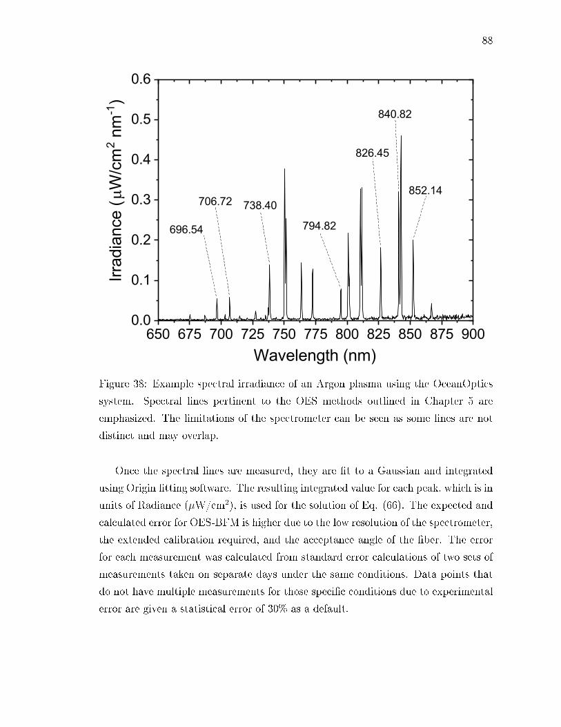
88
650 675 700 725 750 775 800 825 850 875 9000.0
0.1
0.2
0.3
0.4
0.5
0.6
Irrad
ianc
e (m
W/c
m2 n
m-1
)
Wavelength (nm)
696.54
706.72
826.45
840.82
738.40
794.82
852.14
Figure 38: Example spectral irradiance of an Argon plasma using the OceanOptics
system. Spectral lines pertinent to the OES methods outlined in Chapter 5 are
emphasized. The limitations of the spectrometer can be seen as some lines are not
distinct and may overlap.
Once the spectral lines are measured, they are t to a Gaussian and integrated
using Origin tting software. The resulting integrated value for each peak, which is in
units of Radiance (µW/cm2), is used for the solution of Eq. (66). The expected and
calculated error for OES-BFM is higher due to the low resolution of the spectrometer,
the extended calibration required, and the acceptance angle of the ber. The error
for each measurement was calculated from standard error calculations of two sets of
measurements taken on separate days under the same conditions. Data points that
do not have multiple measurements for those specic conditions due to experimental
error are given a statistical error of 30% as a default.

89
6.3 TUNABLE DIODE LASER
An external cavity diode laser was built using a 150 mW Sanyo semiconductor
diode with a nominal free running wavelength of 808 nm in a Littman-Metcalf con-
guration [85]. A picture and schematic of the tabletop laser setup can be seen in
Figs. 40 and 41. This laser was capable of scanning both the 810.37 nm and 811.53
nm transition lines after proper tuning to measure the gas temperature and the 1s4
resonant and 1s5 metastable level densities. The laser can be tuned to a transition by
a coarse adjustment of the grating in the cavity, along with temperature and current
adjustments. Once the laser is tuned to a transition, a piezoelectric device is used to
change incident angle of the laser light by slight adjustments of the mirror mount.
This changes the frequency of the light according to
dν
dθ= −2ac
λ2cos θ, (94)
where θ is the incident angle and a is the grating spacing [86]. At the same time, a
change in the length of the diode laser cavity, or the distance between the diode and
the grating, will cause a frequency shift of
dν
dl= − c
λl. (95)
Oftentimes, a single piezoelectric changing θ is sucient to scan a few GHz in a single
longitudinal cavity mode. However, if the change in angle is too large it will change
the eective cavity length and cause a mode-hop. In our case, the piezoelectric
could only achieve approximately 1 GHz of mode-hop free tuning, which is smaller
than the absorption frequency prole. To address this, one can either add a second
piezoelectric to change the cavity length in sync with the incident angle, or the
frequency of the light can be adjusted to compensate for this change in cavity length.
For the second option, the frequency can be tuned by changing the injection current
(ILD) to the diode. This second option was implemented through the use of a feed
forward circuit, which allows for the simultaneous adjustment of the current and
piezoelectric voltage. In essence, the piezoelectric voltage ramp is used as a time
varying addition to the injection current with the form
∆Vpiezo = Ω∆ILD, (96)
where Vpiezo is the driving voltage of the piezo, and Ω is the circuit resistance in
which the frequency change from the piezo is equal to the change from the current
adjustment, or ∆νpiezo = ∆νcurrent.

90
The feed-forward circuit was built based on a simpler version of the design by
Doret et al. and can be seen in Figure 39 [86]. The combination of the piezoelectric
and feed-forward allowed for a mode-hop free scan of 4 GHz. Absorption proles
were typically ≈ 3 GHz.
Figure 39: The feed forward circuit schematic. The second stage on the right is a
unity gain low pass lter that is only necessary if the signal needs to be inverted.
The feed forward takes the high voltage output from the piezoelectric and yields
a proportional output with an adjustable gain from the potentiometer (R6 in Figure
39). The output signal is adjusted so that ∆ILD = 0 at the middle point of the piezo's
voltage range (∆Vpiezo/2). The value for Ω, and therefore the highest frequency sweep
range, is found by tuning the potentiometer. More details about the feed forward
circuit can be found in Ref. [86].
The laser is guided through an optical isolator into a beam splitter that allows a
portion of the beam to be sent to two dierent Fabry-Perot Interferometers (FPI).
One is a ThorLabs SA200-7A with 1.5 GHz Free Spectral Range (FSR), and the other
is a homemade low nesse parallel mirror interferometer with a calibrated FSR of 303
MHz. Due to the piezoelectric and feed-forward circuit required to get the laser to
sweep over a large enough frequency range, the resulting scan signal has a nonlinear

91
Figure 40: The experimental TDLAS setup (without the FPI systems).

92
scan rate that propagates throughout the scan. Since the laser can only scan 4 GHz
mode-hop free, the 1.5 GHz FSR of the ThorLabs is too large to properly detect
and account for this nonlinearity. The lower FSR of the homemade interferometer
allows for this nonlinearity to be seen over the length of the scan, and the scan can
be calibrated accordingly. The other half of the beam is then split again to be sent
Figure 41: Schematic of the TDLAS tabletop setup.
to a low pressure Ar reference discharge cell for wavelength conrmation and laser
tuning. The other part of the beam is sent to a ip mount that can either send
the beam to a Burleigh WA-20VIS wavemeter or to a ber launcher which sends the
beam to the plasma chamber.
The laser is sent through an unobstructed area of the plasma chamber in front of
the powered electrode by passing through two mini-conat ports as seen in Figure
42.

93
Figure 42: Top: The laser path through the plasma chamber. The laser exits the
ber launcher on the right and passes through a non-polarizing beamsplitter cube
before entering the discharge through the viewport. The laser (minus absorption)
exits the chamber and is collected by the photodiode on the left. Bottom: A cartoon
schematic of the discharge and location of the diagnostic tools. While the laser can
only travel unobstructed through viewport A, the ber optic can be placed at A, B,
or C. However, location A was strictly used for both methods to ensure a more direct
comparison of results.
The beam is collected on the other side of the chamber by a ThorLabs DET100A
photodiode and sent to a 4-channel oscilloscope that measures the laser absorption,
the two FPIs, and the piezoelectric voltage signal (which shows the bounds of the

94
scan). Using the Beer-Lambert law, the absorption signal is converted into the
signal shown in Figure 43 and t to a Gaussian. The resulting Gaussian t yields
all the pertinent information to calculate the gas temperature and density. Each
1 2 3 4 5 6 7 8
0
1
2
3
4
5
6
7
8
0.0
0.5
1.0
1.5
2.0
2.5
0 1000 2000 3000 4000-0.10
-0.05
0.00
0.05
0.10
Volta
ge (V
)
Time (s)
Absorption Signal 303 MHz FPI 1.5 GHz FPI
a) b)
t(n)
Data Gaussian Fit
Residual
dt(n)
Frequency (MHz)
Figure 43: Example of laser absorption measurement using TDLAS: a) Laser ab-
sorption and two Fabry-Pérot Interferometer signals (the piezo voltage signal is not
pictured); b) The processed signal along with residual plot.
measurement consisted of three scans, which were t and then averaged, to ensure
that the scans are consistent and reliable. The error in TDLAS measurements is
calculated from a combination of the error in the Gaussian ts of the prole and the
frequency calibration. The error in these measurements is very small compared to
OES-BFM with an average error of ± 3%.
6.3.1 LASER SCAN FREQUENCY CALIBRATION
The nonlinear jitter caused by the combination of the feed-forward circuit and the
piezoelectric used for the frequency sweeping of the laser requires proper calibration,
without which the nal t can be o by over 100 MHz. The home-built parallel mirror
FPI has a very low nesse and has the form of a cosine wave, but the accompanying
low FSR allows for the measurement and tting of the nonlinear jitter over the scan
length. The 1.5 GHz FSR Thorlabs FPI has a very high nesse and a very low
frequency error, about 3 MHz as stated by the manufacturer. The high FSR is too
large compared to the scan size (approximately 4 GHz) to calibrate the signal for

95
the jitter, but it can be used to properly calibrate the parallel plate FPI and provide
consistency across all measurements. The calibration process works as follows. A
measurement of the two FPIs is taken under typical conditions for a laser absorption
experiment. The signal from the home-built FPI is imported into the Origin data
manipulation and tting software where the background noise is subtracted and the
data is smoothed, yielding a signal that has the form of a cosine function with a time
dependent phase.
Figure 44: Top: The raw home-built etalon signal and the processed signal. Bottom:
The time-varying phase cosine function t to the smoothed data.
This signal is then t according to the following function
V = B cos((E +Dx+ Fx2)x+ p) = B cos(k(x)x+ p), (97)

96
with nal values
B = 0.01316
E = 6.34076
D = 1.0376
F = −0.05061
p = 1.74223,
where E,D, F and p are all dened by the t. It is important to point out that the
values B and p don't matter for the overall calibration of the signal. In fact, the
signal from the etalon is dierent every scan, and one would think that each scan
would need to be calibrated. However, as long as the change in phase is consistent
between scans, the same calibration can be used for every scan. That is to say that
the value of E + Dx + Fx2 must remain the same for every scan. This is done by
setting and not adjusting the piezo voltage, feed-forward, and oscilloscope range.
This is not ideal as it does not allow for adjustment if the system requires it, but
this worked suciently well for our purposes.
Equation 97 can now be used in conjunction with the ThorLabs FPI to calculate
the FSR of the parallel mirror etalon. The total phase change of the cosine function
as measured between the two sharp peaks of the ThorLabs FPI will correspond to
1.5 GHz (the FSR of the FPI). This phase change will then correspond to a specic
number of wavelengths between the two ThorLabs etalon peaks. The number of
wavelengths is then used to calculate the FSR of the parallel mirror FPI according
to
FSR =1.5GHz
N≈ 303 MHz. (98)
With the FSR in hand, the change in frequency as a function of phase can be
calculated by
f =k(x)
2π· 303 MHz (99)
for each value of x. This array of frequency values can then be used to replace the
arbitrary x axis as measured by the oscilloscope and used for the analysis. The
frequency calibration can easily be checked for each scan by plotting the ThorLabs

97
etalon signal vs. the new frequency axis and measuring the FSR compared to the
known 1.5 GHz value as seen in Figure 45. Each scan was within 30 MHz of 1.5
GHz, while most were within 15 MHz. This error is quite small when compared
to the typical 800-900 MHz FWHM of a laser absorption scan. This error, along
with error from the t shown in Figure 44 is propagated through the calculations
of the gas temperatures and the population densities found using laser absorption
spectroscopy.
Figure 45: The ThorLabs etalon and nal t for the Home-Built etalon. One can see
that there are 4.95 wavelengths between the two sharp peaks.
6.4 LANGMUIR PROBE
A single tipped Tungsten Langmuir probe was placed in the discharge to measure
Te and ne independent of purely optical methods. The probe was originally made
by Impedans as an all-in-one measurement device. However, the probe design was
ill-suited for this particular application due to an outdated design in the electrical

98
circuit related to the rf ltering and compensation. More about these particular
issues are discussed in the following paragraph. As it provided no discernible benet,
and a possible source of error, this circuitry was removed from the original probe.
The probe tip is held by an alumina coated metal rod mounted to a mechanical
bellow system seen in Figure 46 that allows the probe to be actively moved (linearly)
in the chamber.
Figure 46: The Langmuir probe housing and linear translation stage.
The probe was inserted at the same location in the chamber as the OES and laser
absorption measurements (see Figure 42). The cylindrical probe tip had a length of 5
mm and a radius of 0.2 mm. While scans were attempted at various radial locations,
the close proximity of the probe to the powered electrode and gas feed made most
locations unusable. This is especially true in those cases in which positive DC bias
was added to the gas feed and/or powered electrode. Regardless of probe position,
the additional DC bias caused the I-V characteristics to be completely unusable.
The most eective probe location was in the radial gap between the inner and
outer electrodes, and thus all presented results were conducted at this position. A
picture of the Langmuir probe in the discharge reactor can be seen in Figure 47. The
probe scans were still measured using the provided software from Impedans, but the
analysis was done independently as the software could not properly characterize the
unltered and uncompensated probe. More details about the independent analysis
procedure can be found in Chapter 8.

99
Figure 47: An end-on photo of the plasma reactor with the Langmuir probe inserted.
A sample for the surface roughness characterization experiment can be seen mounted
in the viewport opposite the probe (red arrow).
As mentioned previously, the probe is limited in its capabilities due to the proper-
ties of the experiment and the initial construction of the probe. The most signicant
limitation of the probe arises from the insucient grounding of the surrounding
discharge about the probe. This is typically done with a second probe tip which
measures the change in the plasma potential (Vp) with the probe potential (V ) and
subtracts this voltage shift from the scan. Without this grounding, Vp can increase
with V , meaning that the probe is directly changing the dynamics of the discharge at
large [87]. This eect is called plasma pulling, and it can make analyzing Langmuir
Probe scans very dicult as the exponential region of the scan is pulled toward
the x-axis, therefore attening the electron current and making the transition region
dicult to discern. While this does make the scan dicult to analyze, it does not
make the scan unusable. Potential pulling occurs because the electron current is large
enough to change the potential of the bulk plasma if it is not appropriately grounded,
or if this change in Vp as V is increased is not measured and removed from the scan.
However, by setting a current limit purposely lower than the maximum range, the

100
exponential region is pulled less due to the limiting of the electron saturation cur-
rent. This essentially shortens the amount of time the scan spends in the electron
saturation region, and thus has a smaller eect on the variance of Vp. If the probe
draws electron saturation current for too long, the probe tip can be heated to the
point of emission, which is not only detrimental to the scan, but also the health of
the probe [87].
A comparison of scans with dierent current limits and examples of plasma pulling
in an Argon discharge is shown in Figure 48. While evidence of plasma pulling can
-40 -30 -20 -10 0 10 20 30 40 50-0.02
0.00
0.02
0.04
0.06
0.08
0.10
0.12
0.14
Cur
rent
(A)
Voltage (V)
1.5 mA 15 mA 150 mA
0 10 20 30-0.005
0.000
0.005
0.010
0.015
0.020 15 mA 150 mA
Figure 48: Example of I-V characteristics for dierent current ranges allowed by the
software. A close up of two of the scans in the region in which they start to deviate
is shown in the upper left corner.
be seen in all scans, it is most evident and problematic for those with a large current
range. All scans share common features in the exponential region of the electron
current, but quickly deviate after the oating potential. The lower current limited
scans have a much better dened exponential region making Te much easier to discern

101
and less ambiguous as the linear region of the ln(I)−V is more clear. Unfortunately,
there is no way to mathematically correct the eects of plasma pulling on the scans
without the measurement of Vp − V , so using traditional methods to nd the EEDF
and Vp (see the Druyvesteyn method in Section 5.1) are not feasible. Therefore,
the use of the scans is limited to calculating Te and ne under the strict assumption
of a Maxwellian EEDF and using the basic Orbital Motion Limited (OML) theory
outlined in Chapter 5. While this is not ideal, the main purpose of the probe is to
compare the results from the CRM to a more widely used measurement method.These
scans are deemed satisfactory for this aim.
In an RF discharge, the harmonics of the RF eld can cause interference in the
probe scan as the probe eectively acts as an antenna. Thus, RF ltering is con-
sidered imperative for a complete and accurate measurement of the discharge EEDF
[49]. However, since plasma pulling has already rendered this outcome impossible,
the importance of RF ltering is minimized. As we are assuming a Maxwellian distri-
bution and specically intend on nding Te and ne, only the linearity of the semilog
I-V characteristic is necessary for this analysis. Indeed, there are a number of works
in which this is explored, and the reader is referred to Refs. [88, 89]. The direct ef-
fects of removing the RF ltering circuitry were negligible to the scan at large, with
the only noticeable change being in the ion current region. A small oscillation can
be seen at a very small scale, but for all intents and purposes this eect is averaged
out when the ion saturation current region is t linearly. This is discussed further in
Chapter 8.
6.5 Nb SAMPLE SURFACE ROUGHNESS EXPERIMENT
niobium samples were produced to study the eect of surface temperature and
electrode positive DC bias on the nal surface roughness prole of plasma etched
niobium at dierent locations in the reactor. The samples were water jet cut from a
sheet of cavity grade Nb provided by Jeerson National Lab. Water jet cutting was
used to eliminate the embedding of silicon and metal impurities from other cutting
techniques. Each sample was diamond paste polished with a Dremel tool so the
samples have as similar a roughness prole as possible. Diamond paste was used to
avoid silicon based polishing methods. Each sample was polished with a series of
pastes with decreasing coarseness down to 1 micron. Most samples were polished to
this 1 micron level, while a small amount were polished to 0.1 microns for post-etch

102
comparison (see Chapter 9). A close up photo of a polished sample before plasma
processing can be seen in Figure 49.
Figure 49: A picture of a Nb coupon sample polished to 1 micron surface roughness.
A mirror-like surface can be seen, along with surface defects like pits and trenches.
These circular coupon type samples were made with the specic intention to
be inserted into the chamber through the DN16 conat viewports. The samples are
then held suspended by a threaded rod in the back of the sample that is connected
to the center of a blank DN16 ange. The length of the rod is such that the sample
is ush with the chamber wall. An example of how the sample is placed in the
reactor can be seen in the right hand side of Figure 47 (red arrow) and a close up
of a mounted sample can be seen in 50. The substrate temperature is measured
for each sample through a type k thermocouple mounted on a vacuum electronic
feedthrough. Four samples were mounted for each experimental run at consistent
locations corresponding to dierent local discharge regions of the coaxial plasma
reactor. These locations are shown in Figure 51. The samples that were polished to
0.1 microns were placed in the sample 4 position in Figure 51. This was done for
comparison as it is expected that samples 2 and 4 will have similar etch proles since

103
Figure 50: The sample mounting and thermocouple setup. The sample is suspended
ush to the chamber wall by the threaded rod. The thermocouple is wired along the
rod and compression t against the back of the sample.
they are in symmetric locations in the chamber.
The substrate temperature was modied externally by wrapping the chamber
rst with conductive heating tape, and then covered with aluminum foil. The tape
was wrapped tightly around the chamber with particular emphasis on even temper-
ature distribution. The temperature of the heating tape was controlled by variac
transformers through the adjustment of the output voltage to the tape. However,
maintaining consistent temperatures between all four samples simultaneously in this
way is dicult. The various local regions of the plasma in the chamber have signi-
cant inuence on the temperature distribution, so there is little control over the `ne
tuning' of temperatures at specic locations. The variation in temperature at each
sample location was monitored throughout the experiment with the highest amount
of uctuations in the rst hour of the etching experiment. After the rst hour, the

104
temperature at each location remained consistent within ≈ 15 o C. Each thermo-
couple was tested for consistency and found to be consistent within 2 ≈ o C of one
another, so this error was ignored. The nal value used for the analysis in Chapter 9
is the average value of temperature measurements taken at consistent time intervals
(typically an hour). The error in temperature is therefore the standard error of the
mean, and is presented as statistical error bars in Chapter 9. The DC bias is adjusted
in the usual way of adding an external positive DC voltage to the powered electrode
through the RF power matching network (see Section 6.1.1).

105
Figure 51: The sample mounting locations. Sample 1 is located at the `rear' of the
electrode. Samples 2 and 4 are located at the center of the corrugated electrode on
opposite sides, and sample 3 is located at the front of the electrode. The chamber
orientation was such that sample 2 is the top of the chamber and sample 4 is the
bottom.

106
CHAPTER 7
DENSITIES OF ARGON EXCITED STATES VS.
EXTERNAL PLASMA PARAMETERS
The following chapter presents results from the measurements taken by Tunable
Diode Laser Absorption Spectroscopy (TDLAS) and the Branching Fraction Method
(OES-BFM). In particular, the 1s4 and 1s5 levels are primarily discussed as these were
measured by both methods and direct comparisons can be made. A comprehensive
summary of the relationship between these densities and the plasma parameters
is outlined, although not all of the data can be included for the sake of brevity.
Pertinent trends, consistencies, and inconsistencies are examined for sets of data
that illustrate eective points clearly and succinctly. Those data that are signicantly
dierent or particularly noteworthy are either addressed in the discussion or presented
separately. Explanations of trends and phenomena are given with literature backing
when available, otherwise educated speculation as to the eects of plasma parameters
(ie. added DC bias voltage) is provided.
Table 5 outlines the external parameters covered in this study. These parameters
are described more in depth in Chapter 2. Each external parameter was treated as a
dependent variable while all other parameters were kept constant. This allows a full
understanding of the eects of each of these external parameters on the measured and
calculated plasma parameters. Combined eects of multiple external parameters can
also be studied as data exists for each external parameter combination. The array
of external parameters was empirically established in previous work for the best
etching outcome, with the Nb etch rate between 60-200 nm/min for the range of
these parameters in this work [68, 36, 38].
This chapter is organized as follows. Firstly, a comparison of the two diagnos-
tic techniques, TDLAS and OES-BFM, are compared as they both have distinct
advantages and disadvantages. This will allow a framework for which the study of
the external parameters to be presented. Secondly, each external parameter will be
considered separately as the eects of each on the resonant and metastable levels
is studied independently. A separate description is presented for both Argon and

107
Table 5: The external parameters studied. The * indicates that these values are not
present for all data sets due to experimental limitations.
Parameter Value Unit
pressure 10*, 25, 50, 75, 100* mTorr
RF power 25, 50*, 75, 100*, 150 W
DC bias self bias, 0, 50, 100 V
Cl2 concentration 0, 1, 5, 10, 15* %
Ar/Cl2 discharges. While this chapter is set to only discuss the eects of the ex-
ternal parameters on the 1s densities, comments about the electron temperature,
electron density, and EEDF are included when important to illuminate physical ef-
fects. Analysis of those particular plasma parameters are outlined in a later chapter.
Lastly, a short discussion summarizing the important outcomes of the study as a
whole is included.
7.1 TDLAS VS. OES-BFM
A signicant motivation for this work is to validate the feasibility of using OES-
BFM to accurately measure the Ar 1s densities in Ar and Ar/Cl2 discharges. Based
on published work there is no reason a priori as to why it couldn't be used in
the cylindrical capacitively coupled plasma (CCP) discharge, but as this system is
distinctly unique, and since there are no published works to directly compare, the
OES-BFM results must be compared to a more accurate method of measurement.
Therefore the densities evaluated from OES-BFM are compared to those measured
from TDLAS. Since TDLAS has the distinct disadvantage of only being able to mea-
sure one transition at a time, and the need for a laser that can be tuned to particular
wavelengths, only certain densities could be compared. However, the closeness of the
810.37 nm and 811.53 nm lines allow for a measurement of both the Ar 1s4 and 1s5
densities with the same tunable laser. OES-BFM has the advantage of being able to
calculate all four lower level densities simultaneously by using an array of measured
spectral lines from a low resolution, high speed spectrometer.

108
In general, a direct comparison of densities measured using TDLAS and OES-
BFM shows consistency within a factor of eight, with the largest discrepancy stem-
ming from the measurements conducted at lower pressures, most prominently those
at 10 mTorr. At 25 mTorr and above, TDLAS and OES-BFM are consistent within
a factor of three for all measured parameters, with a vast majority of those results
well within a factor of two. Published work outlining OES-BFM in comparison to
TDLAS or other experimentally measured results show consistency usually within
a factor of two [58, 59]. Indeed, Li et al. has shown signicant improvement of
OES-BFM results with the use of a mono-directional escape factor instead of the
volume averaged escape factor commonly associated with this method [61]. While
this is a promising modication to the method, we have elected to remain consistent
to the original technique and explore the use of a mono-directional escape factor in
future work. As it stands, the results are suciently consistent to make signicant
qualitative observations, as both sets of measurements vary similarly as a function
of external parameters. This is particularly true for results pertaining to the Ar 1s5
densities as they are more consistent than the 1s4 densities as a whole. These obser-
vations are pointed out throughout the analysis to provide an argument of OES-BFM
as a reliable diagnostic technique.
While OES-BFM is a fast and convenient method, it has a number of limitations
that are being discovered as attempts are made to extend this technique to dierent
types of systems, particularly in mixed Ar discharges. It was the goal of this work to
use OES-BFM in Ar/Cl2 discharges, but there was little to no success. The limita-
tions and proposed reasons why this technique is not eective in Ar/Cl2 discharges
is discussed in the next subsection.
7.2 LIMITATIONS OF OES-BFM
In principle, OES-BFM should work as long as there are enough metastable atoms
to produce measurable changes in the eective branching fraction (for more infor-
mation on the eective branching fraction, see Ref. [11]). With that being said, the
method can fail if there are not enough metastables in the discharge or if the changes
in the branching fractions due to reabsorption cannot be measured. In the case of
this work, there is most likely a combination of both of these problems. Metastable
level densities measured using TDLAS show a drop of upwards of two orders of mag-
nitude when Cl2 is added to the discharge, depending on the concentration. This

109
is not unexpected as the addition of another species, especially one that creates an
electronegative discharge, would reduce the energy and collisions required to popu-
late Ar metastables. In addition, the quenching rate of Ar metastables due to Cl2 is
rather high at 71 × 10−17m3/s [90]. For context, this is about twenty times higher
than N2 and three times higher than O2, two other common plasma discharge ad-
ditives [90]. Wang et al. has shown that OES-BFM can be eective in a 15 mTorr
Ar/O2 inductively coupled plasma (ICP) discharge in concentrations up to 50% [77].
For our case, the partial pressure of Cl2 in our discharge is comparable to Wang's for
many of our measurements, particularly those that are closest to previously estab-
lished etching conditions (15% Cl2 at > 50mTorr). The combination of high partial
pressures and the metastable-Cl2 quenching rate makes OES-BFM a dicult mea-
surement technique for the Ar/Cl2 discharge. At those conditions in which the partial
pressure was very small (1% concentration of Cl2) OES-BFM managed to produce
some reasonable results, but not enough to make clear conclusions.
The necessity of having enough metastable atoms to modify the eective branch-
ing fraction naturally leads to an investigation of the lower limit of the density in
which OES-BFM can be useful. This is not easy to estimate, but the limitations can
be illuminated by considering the form of the photon escape factors for the transi-
tions used in the analysis. A plot of the photon escape factor for a number of spectral
lines used in the analysis is shown in Figure 52.
Figure 52 shows that below 1016 m−3 the change in the photon escape factor
for transitions involving the Ar 1s5 metastable level is quite small compared to the
other transitions. Below 1015 m−3 the photon escape factor is approximately 1 for
all transitions. In addition, it is pertinent to point out that for the conditions of
this discharge the Ar 1s5 density is consistently the highest of the four 1s levels,
sometimes by almost an order of magnitude. Therefore even if the Ar 1s5 density is
in the low to mid 1016 m−3 the other densities may be so much lower that OES-BFM
cannot properly work. The combination of these two issues nicely explains the reason
why realistic results for Ar/Cl2 discharges were seemingly unattainable.
7.3 GAS TEMPERATURE
The gas temperature is a necessary quantity for OES-BFM, and it was measured
for the array of external parameters outlined in the beginning of the chapter. Overall,

110
1014 1015 1016 1017 10180.00.10.20.30.40.50.60.70.80.91.01.11.2
Phot
on E
scap
e Fa
ctor
(g)
Excited State Density (m -3)
826.45 nm (2p 2®1s2) 794.82 nm (2p 4®1s3) 727.29 nm (2p 2®1s4) 696.54 nm (2p 2®1s5) 706.72 nm (2p 3®1s5)
Figure 52: Calculated photon escape factors using Eq. (63) as a function of Ar 1s
population density.
the gas temperature did not vary signicantly as a function of the external param-
eters. In a pure Ar discharge the gas temperature is consistently in the 370-420 K
range with only a few instances of Tg dropping below 370 K. The average gas temper-
ature for the Ar discharge across all external parameters is 391 (± 15) K, which was
rounded up to 400 K for all calculations presented here. This value for Tg is lower
than the temperature in analogous works, but those experimental congurations use
inductively coupled plasmas in a much smaller conguration [57, 58, 82]. Sushkov et
al. [59] conducted similar OES-BFM/TDLAS measurements in a parallel plate CCP
and measured Tg in the range of 320-410 K, which closely matches the Tg range of
this work and has the most similar experimental conditions [59].
The Ar/Cl2 discharge has a larger range of measured values, but in general Tg
remained between 350-450 K. Once again, for ease of use in the OES-BFM data

111
analysis program the gas temperature was approximated to 400 K since the average
Tg across all external parameters is 423 (± 24) K. The gas temperature has been
measured previously for Cl2 containing plasmas and typically show an increase in Tg
as the RF power is increased [91]. However, this is once again an ICP reactor with
much higher RF power upper limits, so we are condent that the values found for
Tg in this work are appropriate.
7.4 RESULTS AND DISCUSSION
We present the 1s4 and 1s5 excited state densities of Ar in both Ar and Ar/Cl2
discharges as a function of external parameters. As stated in Chapter 4, the range of
external parameters is dened based on empirical results of previous etching exper-
iments. Statistical error bars are included on all presented plots, however the error
is oftentimes smaller than the plot symbol size. The 1s2 and 1s3 densities are not
presented in the following section, but on average we have seen n1s4 ≈ 3n1s2 and
n1s5 ≈ 6n1s3. Due to the limitations outlined in Section 7.2, all presented results
involving Ar/Cl2 discharges were measured using TDLAS.
7.4.1 PRESSURE
Ar Discharge
The eects of increasing pressure on the 1s4 and 1s5 levels is well established in
literature, particularly for rf ICPs in pure Ar [57, 58, 82, 92]. In general, there is an
initial increase in both density populations as pressure is increased, with an eventual
plateau and decrease as pressure is increased further. This eect can be explained
in terms of the dominant creation and loss mechanisms of the excited levels in the
discharge. At lower pressures the metastable atoms are primarily lost to diusive
and collisional losses to the resonant levels, while the resonant density is mainly
lost to radiative decay to the ground state. An increase in pressure facilitates an
increase in the electron density, which leads to an increase in excited state density as
more electron-atom excitation collisions take place. Eventually, the electron density
reaches a point where decay from electron-atom collisions (of excited atoms) becomes
signicant enough to lead to a total decrease in the population density. While the
eect can be seen for both populations, the 1s4 density typically shows the eventual
decrease at a higher pressure due to the eects of radiation trapping. Since the only
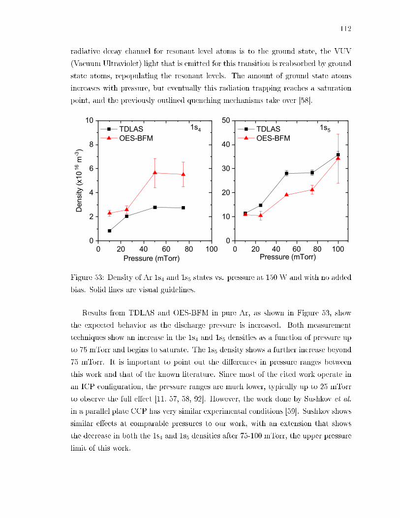
112
radiative decay channel for resonant level atoms is to the ground state, the VUV
(Vacuum Ultraviolet) light that is emitted for this transition is reabsorbed by ground
state atoms, repopulating the resonant levels. The amount of ground state atoms
increases with pressure, but eventually this radiation trapping reaches a saturation
point, and the previously outlined quenching mechanisms take over [58].
0 20 40 60 80 1000
2
4
6
8
10
0 20 40 60 80 1000
10
20
30
40
50
Den
sity
(x10
16 m
-3)
Pressure (mTorr)
TDLAS OES-BFM
1s4 1s5 TDLAS OES-BFM
Pressure (mTorr)
Figure 53: Density of Ar 1s4 and 1s5 states vs. pressure at 150 W and with no added
bias. Solid lines are visual guidelines.
Results from TDLAS and OES-BFM in pure Ar, as shown in Figure 53, show
the expected behavior as the discharge pressure is increased. Both measurement
techniques show an increase in the 1s4 and 1s5 densities as a function of pressure up
to 75 mTorr and begins to saturate. The 1s5 density shows a further increase beyond
75 mTorr. It is important to point out the dierences in pressure ranges between
this work and that of the known literature. Since most of the cited work operate in
an ICP conguration, the pressure ranges are much lower, typically up to 25 mTorr
to observe the full eect [11, 57, 58, 92]. However, the work done by Sushkov et al.
in a parallel plate CCP has very similar experimental conditions [59]. Sushkov shows
similar eects at comparable pressures to our work, with an extension that shows
the decrease in both the 1s4 and 1s5 densities after 75-100 mTorr, the upper pressure
limit of this work.

113
Ar/Cl2 Discharge
The relationship between the Ar 1s5 density and Cl2 concentration is shown for
dierent RF powers in Figure 54 as obtained by TDLAS measurements. An increase
in concentration accelerates the expected trend of the initial rise, then fall of the
density as pressure is increased. This is most evident in the comparison between the
1% and 10% concentrations, as the 1% shows a very similar result as the pure Ar
discharge, while the 10% shows a maximum at 25 mTorr, and a decrease as pressure is
increased. The results for 25 W power show a much more pronounced fall as pressure
is increased past 25 mTorr. This could be due to an increase in the electron density
as power is increased, leading to more electron-atom collisions that could sustain the
production of metastables.
0
3
6
9
12
15
18
0.0
0.5
1.0
1.5
2.0
2.5
3.0
0 25 50 75 1000.0
0.2
0.4
0.6
0.8
0 25 50 75 1000.0
0.1
0.2
0.3
0.4
1% 25 W 75 W 150 W
5% 25 W 75 W 150 W
n 1s5
Den
sity
(x10
16 m
-3)
10%
Pressure (mTorr)
15%
Pressure (mTorr)
Figure 54: Ar 1s5 density measured by TDLAS vs. pressure for dierent concentra-
tions of Cl2 in Ar with no added bias. Solid lines are visual guidelines.

114
7.4.2 RF POWER
Ar Discharge
An increase in RF power while the pressure remains constant serves to increase
the plasma density [11]. While the plasma density, and therefore the electron density,
is expected to increase, the electron temperature Te is expected to remain roughly
constant as the mean free path of the species in the plasma remains the same. This in-
crease in plasma density facilitates an increase in the resonant level densities through
electron-atom collisions from the ground state, and electron-atom collisions of the
metastable levels, forcing a population transfer into the resonant levels. An increase
in the metastable level density as a function of power can be expected for many of
the same reasons, although to a much lesser extent. There is evidence of an increase
of the 1s5 metastable level with power in the literature, but there are also cases where
the density remains constant [11, 57, 59, 82]. The most analogous literature source
to this work, Sushkov, shows an increase and then leveling o of the 1s5 and 1s4
densities, although the trend for the metastable level is much less pronounced [59].
In general, the 1s4 density increases with power at a constant pressure, while the
1s5 density typically initially increases, then decreases. This is particularly true at
lower pressures where the eects of increased pressure, as outlined in the previous
subsection, are not as prominent. Figure 55 shows the eect of increasing power on
the 1s4 and 1s5 densities at 50 mTorr for both TDLAS and OES-BFM measurement
techniques. There is very little change in the 1s4 and 1s5 densities as a function of
rf power. The changes in the densities are not expected to be large, and the small
range of studied powers does not allow for a highly detailed study.
Ar/Cl2 Discharge
The addition of Cl2 in the discharge is expected to show an increase in Ar
metastable level density as RF power is increased [93]. When the RF power is in-
creased the plasma density, and therefore the electron density, will increase, but not
necessarily the negative ion density [93]. Low energy electrons are lost to negative ion
formation in an Ar/Cl2 discharge, while the electron density increases with power.
The increase in electron density facilitates high energy electron collisions with ground
state atoms to produce Ar metastables, while the decrease in low energy electrons
reduces the amount of metastables that are lost to low energy electron mixing [92].

115
2
4
6
8
25 50 75 100 125 1500
10
20
30
40
Den
sity
(x10
16 m
-3)
TDLAS OES-BFM
a)
RF Power (W)
b)
Figure 55: Density of Ar a) 1s4 and b) 1s5 densities vs. RF power measured with
TDLAS and OES-BFM at 50 mTorr with no added bias. Solid lines are visual
guidelines.
Indeed there is a general increase in Ar metastable density as RF power is in-
creased for discharges without added DC bias as shown in Figure 56. The concen-
tration of Cl2 added to the discharge does not have a direct eect on the increasing
trend of density with power, but it is important to keep in mind that the increase in
concentration causes a drastic decrease in Ar 1s state population in general. As the
Cl2 concentration is increased the electron density will decrease to maintain quasineu-
trality. Increasing the concentration will also cause more low energy electrons to be
lost to the creation of negative ions, although this will once again not increase as
power is increased. Although data for only one pressure is shown here, the trend is
consistent across the pressure range studied, with higher pressures typically having
higher densities.

116
0 25 50 75 100 125 150 1750
2
6
8
10
12
n 1s5
Den
sity
(x10
16 m
-3)
RF Power (W)
1% Cl2 5% Cl2 10% Cl2 15% Cl2
Figure 56: Ar 1s5 density measured by TDLAS vs. RF power for dierent concen-
trations of Cl2 in an Ar/Cl2 discharge at 50 mTorr with no added bias. Solid lines
are visual guidelines.
7.4.3 DC BIAS
The negative dc self bias that forms on the powered electrode due to the blocking
capacitor in the RF power circuit leads to a larger potential drop between the plasma
bulk and the powered electrode across the corresponding sheath. In semiconductor
processing, this can be an advantage as the substrate can be placed on the powered
electrode to take advantage of the high ion acceleration energy. In our case however,
the goal is to etch a large grounded outer surface. This is not possible without the
use of a positive DC bias on the powered electrode due to the asymmetric discharge
conguration [7]. The positive DC bias essentially serves to ip the discharge asym-
metry that causes a larger voltage drop between the plasma bulk and the smaller

117
powered electrode, thus making the larger grounded electrode the surface with the
largest voltage drop. This leads to larger ion energy and ion ux into the grounded
surface and provides the physical energy component of IARIE. Further explanations
of the eect of positive DC biasing on etching mechanisms and results can be found
in previous work [7, 8, 36].
The eect of DC biasing on rf CCP etching reactors has been studied by a number
of research groups, both experimentally and with particle-in-cell simulations [3941,
9496]. However, a majority of this work was done to study the addition of a negative
added bias on either the powered or grounded electrodes, rather than a positively
added bias. While these works are useful for gaining a general understanding of the
eects of DC bias on the discharge, the complete picture for the purposes of SRF
cavity etching remains incomplete. Understanding the relationship between the Ar
1s states, and later Te and ne, and total positive DC bias will provide better insight
into the eect of DC bias on the plasma dynamics.
Ar Discharge
The eects of DC bias on the 1s5 densities can be seen in Figure 57. The in-
troduction of a positive DC bias causes a decrease in the 1s5 density, with a larger
drop as the pressure is increased. For most cases, increasing the bias has no sig-
nicant eect on the density, with the exception being when the pressure is higher.
Although an increase in 1s5 density with DC bias is seen for 100 mTorr, the overall
increase is rather small. A subtle drop in density can been seen for 75 W and 150
W, particularly for the higher pressures, but the eect is essentially within statistical
error.
A comparison of TDLAS and OES-BFM for the 1s4 densities (not shown) show
similar trends as seen in Figure 57, and results from OES-BFM show an overall drop
in density as positive DC bias is introduced for each 1s density (including the 1s2 and
the 1s3 densities). Both measurement techniques show essentially the same trends,
including the increase in density with DC bias at higher pressure.
The decrease in the 1s densities as positive bias is introduced could be due to
an increase in ionization of these states and a total increase in the plasma density.
Indeed, there are multiple studies that show an increase in ion/electron density as
bias becomes more positive [95, 96]. As the powered electrode becomes positively
biased the electron current increases through this surface with an increased energy.

118
0
10
20
30
40
50
60
0
10
20
30
40
50
0 50 100Self Bias0
10
20
30
40
50
0 50 100Self Bias
10 mTorr 25 mTorr 50 mTorr 75 mTorr 100 mTorr
75 W
150 W
n 1s5
Den
sity
(x10
16 m
-3)
DC Bias (V) DC Bias (V)
25 W
75 W
150 W
OES-BFMTDLAS25 W
Figure 57: Ar 1s5 density vs. DC bias for 25, 75, 150 W power measured with
TDLAS and OES-BFM. The dashed lines indicate the negative bias region outlined
in Section 7.4.3.

119
This eect was recorded by measuring the current through the dc power supply that
provides the positive bias. These electrons then cause high energy secondary electron
emission from the powered electrode that can eectively ionize neutral atoms in the
discharge. In addition, the larger electric elds in the rf sheath and the bulk result in
more forced ionization processes [96]. Total positive DC biases serve to increase the
plasma volume inside the discharge chamber, while total negative biases restrict the
discharge to the smaller region between the two electrodes [96]. The positive bias
eectively pushes the discharge throughout the chamber as the entire grounded
surface (with a much larger surface area) becomes the most attractive surface for
ions in the discharge, and the powered electrode becomes the least. This expansion
of plasma volume is conrmed qualitatively by observation of the discharge as positive
bias is added. In addition, a measured increase in electron current as positive DC bias
is introduced and then increased means that an equal ion current must be owing
through the grounded surface due to conservation of current.
Ar/Cl2 Discharge
In general, the behavior of the Ar 1s5 density as a function of bias in Ar/Cl2
discharges is similar to the relationship outlined in a pure Ar discharge. This is par-
ticularly interesting because of the large dierence in the densities as the addition
of Cl2 reduces the density by two to three orders of magnitude. However, the rela-
tionship between density and DC bias changes as other external parameters, most
particularly pressure and power, are varied.
Figure 58 shows the relative Ar 1s5 density as a function of DC bias for 25 mTorr
and 100 mTorr. The trends for the 25 mTorr set show very similar behavior as in
pure Ar as the density drops when positive bias is introduced, and remains relatively
constant as the bias is increased. For higher pressures. however, it seems that the
increase in bias does much less to decrease the density, particularly for higher powers.
In addition, the increase in bias also has an eect in increasing the Ar 1s5 density,
even to the point in which it surpasses the value for self bias. No explicit explanation
for this behavior can be oered at this time, but forthcoming analysis of the electron
temperature, electron density, and EEDF will serve to help provide answers.
7.4.4 CL2 CONCENTRATION
The addition of Cl2 in an Ar discharge adds a great deal of complexity to the

120
0.0
0.1
0.2
0.3
0.4
0.5
0 50 100Self Bias0.0
0.1
0.2
0.3
0.4
n 1s5
Den
sity
(x10
16 m
-3)
25 W 75 W 150 W
25 mTorr
100 mTorr
DC Bias (V)
Figure 58: Ar 1s5 density measured by TDLAS vs. DC bias for 15% Cl2 in an Ar/Cl2
discharge. The dashed lines indicate the negative bias region outlined in Sec. 7.4.3.
Solid/dashed lines are visual guidelines.
kinetics and charge particle balance of the plasma. An Ar/Cl2 plasma is electronega-
tive, which means there is an additional negatively charged species, namely negative
Cl ions in this case, in the discharge. However, the quasineutrality condition does not
change and the total amount of positive and negative species in the discharge (macro-
scopically) must be equal. With an additional negative species in the discharge, the
amount of electrons will naturally decrease, and therefore the amount of electronic
collisions will decrease. In addition, there are a number of new electronic excita-
tion channels involving Cl2, such as molecular and atomic ionization, dissociative
attachment (Cl− formation) and dissociation (molecular splitting) [54]. As previ-
ously mentioned in Section 7.2, the Cl collisional quenching rate of Ar metastable
and resonant level densities is quite high compared to other commonly used molecu-
lar gases in discharges [90]. With all of these new processes in mind, it should not be
surprising that the Ar 1s4 and 1s5 densities are expected to decrease as Cl2 is added

121
0.1
1
10
0.1
1
10
1 3 5 7 9 11 13 150
0.1
1
10
1 3 5 7 9 11 13 150
10 mTorr
n 1s5
Den
sity
(x10
16 m
-3)
Self Bias 0 V 50 V 100 V
25 mTorr 50 mTorr
75 mTorr
Cl2 Concentration (%)
100 mTorr
Figure 59: Ar 1s5 density measured by TDLAS vs. Cl2 concentration at 75 W. Solid
lines are visual guidelines.
to the discharge. Indeed, there are a number of sources that have shown theoretically
and experimentally that this is the case for dierent types of discharges [54, 92, 97].
While the general eect of Cl2 concentration on the Ar 1s densities is known, the
experimental conrmation between this work and outside sources is important. It
is also pertinent to study the eects of Cl2 concentration as it pertains to the other
external parameters, particularly DC bias, for etching experiments.
The eect of increasing Cl2 concentration on the Ar 1s5 density for dierent pres-
sures is shown in Figure 59. In all cases, just a 1% concentration of Cl2 signicantly
decreases the Ar metastable density, with an eventual leveling o as the concen-
tration is increased. This relationship matches very closely to previously published
work involving the study of Ar metastable density and Cl2 concentration, as well as
relationships established with other molecular gases [60, 97]. The comparison to the
work done by Scheller et. al. is quite intriguing, with the data trend being almost

122
identical [97]. However, Scheller does show an initial increase in Ar metastable den-
sity at very low concentrations of Cl2 in Ar [97]. This increase was not seen for any
of the measurements made in this work, but this is most likely due to experimental
limitations as very low Cl2 concentrations (<1%) are required. Scheller explains that
the initial increase in metastables at low Cl2 concentrations is due to a decrease in
metastable relaxation as low energy electrons are consumed by attachment processes
of Cl2 [97]. As the concentration increases, the collisional quenching processes quickly
become dominant and the Ar 1s5 density decreases accordingly.
The amount of Ar metastables that are lost when Cl2 is added is signicant, with
a typical drop of two orders of magnitude as the concentration is increased from 0%
to 15%. This large drop in Ar metastable density as measured by TDLAS gives
additional credence to the limitations of OES-BFM outlined in Sec. 7.2. Typical
values of the Ar metastable density at concentrations above 5% are in the 1014−1016
m−3 range, with the larger values attributed to the self bias results.
7.4.5 CONCLUSIONS
Among the external parameters studied in this work, the external DC bias is
arguably the most important as it is directly related to the eectiveness of the etching
of niobium and SRF cavities. In many cases, a negative external bias is added to
either electrode to increase the ion energy into that surface and to assist in etching.
As the desired surface to be etched is the inside surface of a grounded cylinder, a
positive DC bias is added to the powered electrode to ip the natural asymmetry
caused by the unequal surface areas and force ions into the grounded surface. When
positive DC bias is added to the powered electrode, the density of all 1s states drops
signicantly, but does not necessarily continue to change as bias is increased. Studies
conducted on the eect of DC bias have shown that the plasma density increases as
the DC bias on the powered electrode becomes more positive [40, 41, 95, 96]. A drop
in Ar 1s densities as the plasma density increases is indicative of increased ionization
of the 1s states and the 2p states that populate them.
Two dierent non-invasive spectroscopy techniques were used to measure the den-
sity of the rst four excited states of Ar in a coaxial cylindrical rf CCP designed for
the plasma processing of SRF cavities. These excited state densities were measured
for both Ar and Ar/Cl2 mixtures of varying concentrations as the Ar/Cl2 mixture
is necessary for etching of these cavities. The two measurement techniques, TDLAS

123
and OES-BFM, were conducted in tandem as pertinent external parameters were
varied to develop a working model to describe this particular discharge. While TD-
LAS is a much more accurate measurement technique, it requires the use of a tunable
diode laser. In addition, TDLAS can only measure one density at a time as it re-
quires the laser to be tuned to a specic atomic transition. OES-BFM has gained
popularity since its introduction by Schulze and further implementation by Board
[57, 58]. This optical method is advantageous due to its ability to measure all four
Ar 1s state densities simultaneously using inexpensive low-resolution spectroscopy
systems. Similar to the TDLAS method, OES-BFM avoids any requirement that
knowledge of the EEDF must be known a priori as the method does not require the
use of any collisional cross sections. However, this method is not nearly as accurate
as TDLAS and the use of a low-resolution spectrometer in favor of speed can be a
detriment when using a variety of strong and weak lines in the analysis. In addition,
OES-BFM is limited in its ability to measure these densities for multi-gas discharges,
especially when Cl2 is involved, due to much lower excited state densities and much
higher photon escape factors.
As a direct comparison, TDLAS is much more eective than OES-BFM at mea-
suring the excited state density with accuracy and consistency. The results of this
work show agreement between the two methods up to a factor of three for the vast
majority of the external parameters studied, which is consistent with other studies
[5861]. At a minimum, OES-BFM is eective in modeling qualitative relationships
between the excited state density and the external parameters, especially in regards
to pressure and DC bias. This can be quite useful to gain a quick yet eective
understanding of a discharge.

124
CHAPTER 8
EFFECTS OF EXTERNAL PARAMETERS ON THE
ELECTRON DISTRIBUTION
The study presented in the previous chapter outlined some very useful techniques
to gain a better understanding of a low temperature discharge, but the full descrip-
tion is far from complete. Explicit information regarding the EEDF, particularly Te
and ne, provide direct connections between the plasma parameters and the etching
mechanisms. The electron temperature and density are related to both the physical
and chemical etching components of IARIE as electrons are responsible for the vast
majority of excitation and ionization processes. This information can be attained
in a number of ways, but is commonly found through Collisional Radiative Models
(CRMs) and electrical Langmuir Probes. Both of these methods are employed in this
work, and the details of which are described in Sections 5.1, 6.4, and 5.3. Presented
here are the results of applying those methods utilizing the results and observations
from the spectroscopy diagnostics in the previous chapter. Results are presented
rst for pure Argon discharges, with a shorter section dedicated to Ar/Cl2 discharges
at the end of the chapter. Due to the experimental limitations of the OES-BFM
technique, its direct application to Ar/Cl2 discharges was not possible, and therefore
similar limitations exist for the application of the CRM. Thus, the results for Ar/Cl2
are incomplete and still require further work.
8.1 Te AND ne MEASUREMENT AND CALCULATION SOURCES
As outlined in Chapter 5, there are a number of dierent ways to measure the
electron temperature and density. Furthermore, the use of Eq. (83) (Section 5.3)
allows for an alternate calculation method in which measurements from multiple
sources can be used in conjunction. This is particularly useful because the 1s state
densities measured from TDLAS can be used in Eq. (83) to calculate ne by using Te
measured from the CRM and Langmuir Probe (LP), allowing for direct comparisons
of consistency between measurement channels. The CRM and LP can be used to
calculate both Te and ne, although the LP can only do so in the case where there is

125
no added bias due to the limitations outlined in Section 6.4. The combinations for
calculating ne using Eq. (83) are presented in Table 6.
Table 6: The parameter combinations for calculating ne using Eq. (83). NR refers
to the ratio of 1s5/1s4. The LP results can only be used for discharge conditions
without added DC bias.
Combined Methods for ne
NR Te
OES-BFM CRM
TDLAS CRM
TDLAS LP
8.2 LANGMUIR PROBE RESULTS
The Langmuir Probe scans were analyzed using the simple Orbital Motion Lim-
ited theoretical treatment presented in Section 5.1. An example of a typical Langmuir
Probe scan is shown in Figure 60.
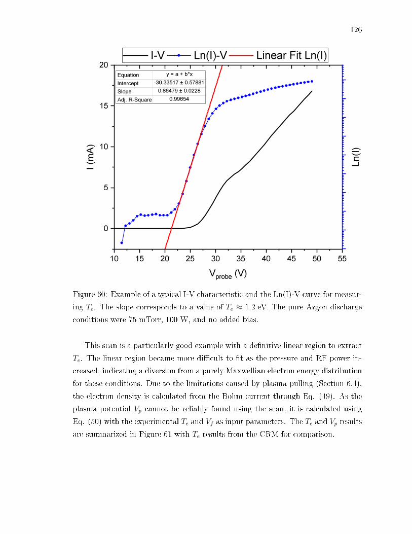
126
Figure 60: Example of a typical I-V characteristic and the Ln(I)-V curve for measur-
ing Te. The slope corresponds to a value of Te ≈ 1.2 eV. The pure Argon discharge
conditions were 75 mTorr, 100 W, and no added bias.
This scan is a particularly good example with a denitive linear region to extract
Te. The linear region became more dicult to t as the pressure and RF power in-
creased, indicating a diversion from a purely Maxwellian electron energy distribution
for these conditions. Due to the limitations caused by plasma pulling (Section 6.4),
the electron density is calculated from the Bohm current through Eq. (49). As the
plasma potential Vp cannot be reliably found using the scan, it is calculated using
Eq. (50) with the experimental Te and Vf as input parameters. The Te and Vp results
are summarized in Figure 61 with Te results from the CRM for comparison.

127
Figure 61: Te (left axis) and Vp (right axis) as measured from the Langmuir Probe.
The results from the CRM for similar discharge conditions are included for compar-
ison.
In all cases, the Langmuir Probe underestimates Te compared to the CRM, in
some cases up to an eV. The plasma potential shows a steady increase with RF
power as it should since the plasma potential is directly related to the amount of
ions in the bulk of the discharge. Increasing RF power leads to an increase in the
plasma density, therefore leading to an increase in Vp. Overall, the Langmuir Probe
results are encouraging as Te and ne (presented later in the chapter) are within the
expected range for this discharge. However, that is the extent of the usefulness of
the probe results as the experimental limitations provides too much uncertainty in
their validity. It is for this reason that these results are presented without error,
as they serve to merely act as a comparison and conrmation of trends seen in the
CRM. Additionally, the inability of the probe to work eectively with the inclusion
of a positive DC bias on the driven electrode greatly limits the probes applicability.
8.3 CRM RESULTS AND SELF-CONSISTENCY
The electron temperature and density was calculated following the model outlined
in Section 5.3, but it is pertinent to discuss how the nal values were decided. As was

128
stated in 5.3, Te and ne were calculated independently for each spectral line using Eq.
(81) and 82 respectively. The nal value for each of these quantities is therefore
the average of the individual calculations, with the error being the standard error of
the mean. Table 7 shows a typical example of the nal results calculated using the
CRM.
Table 7: Results from the CRM for a pure Argon discharge at 50 mTorr, 150 W, and
with no added DC bias.
Originating Level 2p2 2p3 2p4
Wavelength (nm) 826.45 696.54 840.82 738.40 706.72 852.14 794.82
Te (eV) 2.76 2.76 2.20 2.20 2.20 3.44 3.44
ne (1017 m−3) 7.78 7.78 21.0 21.0 21.0 3.21 3.21
It is plain to see that the results are consistent for lines that originate from the
same upper level. Additionally, the relationship between results is consistent for all
experimental conditions with the 2p4 lines having the highest Te (lowest ne), the 2p3
lines having the lowest Te (highest ne) and the 2p2 lines being in the middle. The
values in Table 7 are among those with the highest spread, while the majority of
results are consistent well within 1 eV. When a positive DC bias is applied on the
driven electrode, the same trend exists but with the spread being much smaller. The
most likely explanation for this behavior lies in the uncertainty of the transmission
rates Q used for each transition. As each 2p level is going to use the same rates in Eq.
(81), it would follow that the results should be consistent for those lines originating
from that level. Since this is indeed the case, it shows that the model is eective as
the experimental values used in the left hand side of Eq. (81) are certainly dierent
for each spectral line ratio. While the consistency within 2p levels is encouraging,
the reason for the spread of the values as a whole remains unknown at the present
time.
8.4 THE ELECTRON TEMPERATURE AND DENSITY AS A
FUNCTION OF EXTERNAL PARAMETERS
In the following section, Te and ne results from the CRM are presented as a
function of the external parameters found in Table 5. It is important to reiterate that
these results assume a Maxwellian distribution for the electron energy. There exist
several indicators that the EEDF diverges from this form under certain conditions,

129
which will be explained in the text. Once again, statistical error bars in the form of
standard error are included for each plot, but the error bars may be smaller than the
plot symbol size.
The electron temperature and density as a function of RF power for each pressure
and bias conguration is shown in Figure 62.
2
3
4
0 0
20
40
60
2
3
0 0
20
40
60
80
100
2
3
0 0
20
40
60
2
3
0 0
20
40
60
25 50 75 100 125 150
2
3
025 50 75 100 125 150
0
20
40
60
10 mTorr 10 mTorr
25 mTorr 25 mTorr
50 mTorr 50 mTorr
75 mTorr
100 mTorr
75 mTorr
100 mTorr
NB 0V 50V 100V
T e (e
V)
NB 0V 50V 100V
Ne (
x1017
m-3
)
RF Power (W) RF Power (W)
Figure 62: Electron Temperature (Left) and Density (Right) vs. RF power. Solid
Lines are visual guidelines.
It is expected that there be little variation in Te with RF power while ne should
increase, according to global particle and energy balance considerations respectively
[2]. This is indeed the case for all conditions shown in Figure 62 except for those

130
results at 100 mTorr. For the results involving a positive DC bias, the expected
trend seems to reverse course as Te increases with increasing RF power and ne sees
an initial reduction, but little change with further increase in power. Without added
DC bias, Te and ne remain essentially constant as a function of RF power. This
seems to mark a transition region of the discharge to a non-Maxwellian distribution.
As 100 mTorr was the upper pressure limit of this work, further investigation would
be required to study this transition region fully.
The eects of pressure and DC bias can be seen in Figure 62, but plotting Te and
ne as a function of the DC bias provides additional clarity as shown in Figure 63. It
Figure 63: Electron Temperature and Density vs. DC bias for 25 W, 75 W and 150
W.
is evident that the addition of a positive DC bias on the powered electrode causes
a decrease in the electron temperature and increase in the electron density. Indeed,
this exact outcome was proposed in the previous chapter as the 1s4 and 1s5 densities
also decreased with the addition of positive DC biasing. It is important to reiterate
here that this is indicative of an increase in the ionization of the excited states as
opposed to ground state atoms. Much like the 1s state densities, the transition
from negative to positive bias voltage has a much larger eect on Te and ne than
the further increase of the voltage in the net positive region. These results hold a
striking similarity to those of Zuener et al. in which the eects of a variable DC bias

131
(placed on the powered electrode) on the ion densities was studied in a parallel plate
Argon CCP [96]. Their measurement of the ion density as a function of DC bias
show a very similar increase and sharp plateau for a number of dierent discharge
powers once the total DC bias crosses the positive axis. In the same study, the ion
current into each electrode was measured as a function of DC bias. At the powered
electrode, the ion current shows a similar increase and eventual plateau at VDC = 0,
while the ion current into the grounded electrode continues to increase slightly with
increased positive bias [96]. These eects are attributed to the plasma adjusting to
the most stable state as the plasma potential is changed. The plasma potential VP is
always the highest potential in the discharge (see Section 2.3) and thus must increase
as the DC bias becomes more positive. The plasma compensates for this by conning
electrons in the bulk to increase ionization processes, which are then emitted to the
electrodes [96].
Additionally, there have been a number of theoretical studies of the eect of DC
bias on the particle and energy distributions in a parallel plate CCP [41, 42, 94, 95].
While most of these primarily study the eect of adding a negative bias on one
of the electrodes, they all conrm the results shown in Figure 63. Particularly, as
the bias is used to reverse the asymmetry, the plasma density is increased in the
bulk between the two electrodes and further conned. Additionally, the electron
temperature decreases under the same eects, with a minimum at the location of the
highest density (see Figs. 3 and 4 in Ref. [42]).
The eect of increasing the discharge pressure in the positive bias regime can also
be seen in Figure 63. In the majority of cases, the electron temperature decreases with
pressure, while the electron density increases. This is due to the increase in collisional
processes in the discharge with higher pressure, therefore decreasing the average
energy of the electrons. However, these respective eects become less prominent as a
whole with an increase of the RF power, with the 100 mTorr set completely traversing
the trend for both Te and ne. As mentioned above, this indicates a transition in the
EEDF with the combination of high pressure, high power, and a total positive DC
bias. Figure 63 provides additional evidence for this conclusion as no discernible
trend between ne and pressure can be seen for the highest RF power (Bottom right
panel of Figure 63). As the eect of pressure for the non-biased results cannot be
seen clearly in the above gures, these results are plotted by themselves in Figure
64.

132
Figure 64: Te and ne vs. Pressure for discharges without added DC bias. Solid lines
are visual guidelines.
As a whole, there doesn't seem to be any relationship between the pressure and
Te/ne. The expectation is that as one of the parameters trend in one direction,
the other parameter would trend in the opposite direction, much like those results
for positive biases. While this can be seen in small instances, they are well within
the statistical error and are therefore inconclusive. The explanation for the lack of
variation with pressure remains unknown.
8.5 THE CALCULATION OF ne USING THE COMBINATION
METHODS
The results for ne as a function of the external parameters are presented for the
multiple measurement/calculation sources outlined at the beginning of the chapter.
The combination methods are labeled in the format NR/Te throughout this section
as according to Table 6. When the CRM was used as the Te input source, ne was
calculated for each spectral line and averaged in the same way as the self-consistent
CRM. In the cases where the ne results from the Langmuir Probe are included,
they are presented without error only for comparative purposes. In the case of the
combined treatment utilizing 1s densities from TDLAS and Te from the Langmuir
Probe, the data is presented with error bars of ± 30 %.
The electron density as a function of the RF power are shown for 50 and 75 mTorr
in Figure 65 and 66 respectively.

133
Figure 65: ne vs. RF power at 50 mTorr for each DC bias conguration. Solid lines
are visual guidelines.

134
Figure 66: ne vs. RF power for a pressure of 75 mTorr in each DC bias conguration.
Solid lines are visual guidelines.
In general, all of the dierent methods show the same general trends as a function
of RF power. It is noteworthy that the self-consistent CRM and the OES-BFM/CRM
combination, which both use the same 1s4 and 1s5 densities, typically overestimate ne
compared to the other methods. The self-consistent CRM has the largest statistical
error, while the TDLAS/CRM combination has the lowest statistical error. This is
not surprising as TDLAS is the more accurate method in measuring the 1s state
densities.
The electron density as a function of the DC bias for 50 and 75 mTorr is shown
in Figure 67.

135
Figure 67: ne vs. DC bias for each RF power with discharge pressures 50 and 75
mTorr. The dashed lines indicate the negative bias region outlined in Section 7.4.3.
All of the ne calculation methods show an increase as a function of DC bias as
was presented in the previous section. This is encouraging as the eect transcends
the NR measurement source. As the TDLAS/CRM combination show the most
consistent trends with the lowest error, this combination is shown for a greater array
of experimental conditions in Figure 68.

136
Figure 68: ne vs. DC bias for dierent discharge pressures. All data was calculated
using the TDLAS/CRM NR/Te combination.
The results from the TDLAS/CRM combination show similar trends and densities
as those presented in Figure 62, but with even more consistency. Additionally, the
eect of increasing the discharge pressure remains consistent for a greater range of
parameters, including the results without added bias. A similar reverse of the trend
occurs for the higher power and DC bias, but to a much lesser extent than was seen
previously.

137
8.6 Ar/Cl2 RESULTS
The application of the CRM to Ar/Cl2 is challenging due to the inability to nd
the 1s densities using the OES-BFM diagnostic method (see Section 7.2). Addi-
tionally, TDLAS was used to nd the 1s5 density in Ar/Cl2 mixtures, but the 1s4
density was not. Therefore, the direct application of a fully self-consistent CRM is
not feasible. However, Figure 59 in Section 7.4.4 shows the relationship between the
1s5 density and the Cl2 concentration of the discharge. In each case, there is a con-
sistent trend with the increase of Cl2 that closely follows the relationship found by
Scheller et al. [97]. By applying this same relationship to the other 1s state densities
measured in pure Argon, the CRM can be used just as before to calculate Te and
ne. This can also be applied to the 1s4 densities measured by TDLAS, so that the
TDLAS/CRM combination method can be used as well. We believe this approxi-
mation is appropriate as the collisional quenching rate between Ar and Cl2 atoms is
the same for the metastable and resonant levels (71× 10−17m3/s). Additionally, due
to the large reduction in densities with the introduction of Cl2, photon reabsorption
is negligible as the photon escape factor approaches 1 (see Eq. (65)). Therefore, it
stands to reason that all of the densities would follow the same general trend with
an increase in Cl2 concentration.
An example of the application of this approximation is shown for an Ar/Cl2
discharge with 90% Argon and 10% Cl2 at 75 mTorr in Figure 69.

138
Figure 69: Te and ne vs. RF power for pure Argon (solid symbols) and Ar/Cl2
(90/10 %) for each DC bias conguration at 75 mTorr. Te was found using the
CRM, while ne was found using the TDLAS/CRM combination method. Lines are
visual guidelines.
It is rst important to point out that the ne results calculated by the CRM
and the OES-BFM/CRM combination methods are not shown as these methods,
particularly the CRM, overestimate the electron density by a great deal. As the
calculation of the electron temperature was not dependent on ne (ne is canceled in
the ratio method Eq. (74)), these values were not considered inaccurate. However,
this means that the only dierence between the calculation of ne in Ar and Ar/Cl2 is
the input Te as the ratio NR is the same. Therefore, the ratio of the pure Ar ne and
Ar/Cl2 mixture is strictly dependent on the ratio of the electron temperatures. Due
to the addition of Cl2, the discharge becomes electronegative, meaning that there is
an additional negative species (Cl−) in the discharge. Naturally, this means that the
electron density should decrease to maintain quasineutrality. The experimental work
in an ICP by Fleddermann indeed shows a decrease in ne as the Cl2 concentration

139
is increased, but there are two distinct regions for low and high concentrations [93].
Below 40% Cl2, the electron density is much higher than expected, with ne only
decreasing by a factor of 2 from 0 to 10 %Cl2. Additionally, measurements by the
same group show that the electron temperature does not change signicantly between
Ar and Ar/Cl2 discharges at lower Cl2 concentrations [92]. Due to these discrepancies,
additional work must be done to fully understand the Ar/Cl2 discharge in our context.
8.7 GENERAL CONCLUSIONS
The electron temperature and density for a pure Argon discharge in a coaxial
CCP have been measured as a function of a number of external parameters pertinent
to RIE using a collisional radiative model. Particularly, the relationship between
Te/ne and DC bias is consistent with both experimental and theoretical works for
parallel-plate CCPs [41, 42, 9496]. A decrease in Te and increase in ne is seen as
the DC bias on the driven electrode switches from negative to positive. This nicely
explains the trends seen in the previous chapter as the 1s state densities decrease in
the same manner as Te. This indicates that the ionization of the 1s states increases
with this transition in bias, contributing to a higher ne. A positive DC bias also
forces an increase in the plasma potential which encourages ionization processes by
conning electrons in a tighter region between the electrodes. A combination of
a positive DC bias, high pressure, and higher powers shows a transition region in
which the EEDF deviates from a Maxwellian distribution. This can be useful when
determining operating conditions for a plasma etching experiment.
Additional to the CRM, the electron density was calculated in multiple ways by
utilizing a simple relationship developed by Li et al. [61, 81]. The ratio of the 1s5 and
1s4 densities calculated from the diagnostic methods outlined in Chapter 5 was used
as an input parameter in conjunction with the electron temperature measured by the
CRM and Langmuir Probe. In general, all of the various methods show consistent
trends and results as a function of the external parameters. The combination of the
density ratio from TDLAS and Te from the CRM show the most consistency.
The CRM and TDLAS/CRM combination method were applied to an Ar/Cl2
discharge in a similar manner as the pure Argon discharge. However, approximate
values for the 1s2,1s3, and 1s4 densities were used based on the relationship between
the 1s5 density and Cl2 concentration found in the previous chapter. While this
approximation seems appropriate, further work is required to conrm the results

140
found using this relationship.
8.8 COMPARISONS TO TRADITIONAL REACTORS AND
CONNECTIONS TO REACTIVE ION ETCHING
At this point, it is pertinent to outline particularly interesting results and make
appropriate connections of the plasma parameters to the mechanisms of RIE. Among
the most surprising and intriguing results of this work are those pertaining to the
electron density. In particular, the high value of the 1s states and ne for the con-
ditions of this work illuminate the benets of this reactor. Among the types of low
temperature discharge sources, the CCP typically has the lowest plasma density in
the range of 1015 − 1017 m−3. Higher densities are reached by using ICP's or helicon
based electron cyclotron resonance (ECR) sources with typical values in the range of
1016 − 1018 m−3 or higher [2]. The astute reader will notice that the plasma density
measured in this work is very high for a CCP as the values are consistently in the
range of 1017 − 1018 m−3. Indeed, this remains true when comparing the 1s state
and electron densities to the works that are frequently cited throughout this disser-
tation, regardless of the plasma source [11, 57, 58, 60, 65, 68, 74, 76, 77, 98]. The 1s4,
1s5 and electron densities are typically 1-2 orders of magnitude higher compared to
these outside works. It it important to emphasize that this is true while many of the
basic relationships that have been well understood between the plasma and external
parameters remain. The consistency of the results in this work between the various
diagnostic methods rmly establishes that, at the very least, the order of magnitude
of these densities are undeniable.
These higher densities at the comparable RF powers and discharge pressures of
the other works is a signicant boon to the etching mechanisms of RIE. The higher
ion density (due to quasineutrality) is an obvious benet as they are the `fuel' of
the etching process. Additionally, in the case of pure Argon discharges, there are
no external parameters that lead to the quenching of electron/ion pairs, at least
below 100 mTorr. The simple relationship between the electron temperature/density
with DC bias, while expected, is useful as the amount of change is quantiable and
constant with the increase of positive DC bias. This can provide someone with the
means to establish a more sophisticated model of this discharge as a function of the
external parameters with the goal of understanding the ion energy distribution. It
was also shown that the operation at a lower pressure is quite benecial, especially

141
when a positive DC bias is involved, as the plasma density is certainly high enough to
facilitate RIE processes while the plasma remains simple in characterization. This is
particularly useful for experimentalists as considerations regarding the experimental
apparatus and its longevity are always a concern, especially when halogen gases
are involved. While results including Cl2 remain elusive for the time being, it is
important to keep in mind that the addition of Cl2 at these lower concentrations
are not expected to decrease the electron density in a signicant manner. Thus,
the important energy providing electrons remain abundant in an Ar/Cl2 discharge.
These conclusions are not only important for the RIE of Nb cavities, but for the
technology of RIE as a whole as the unique reactor geometry/style could provide a
solution to processes that require a high plasma density at lower pressures and RF
powers.

142
CHAPTER 9
SURFACE CHARACTERISTICS OF PLASMA ETCHED
Nb SAMPLES
The empirical study of Reactive Ion Etching (RIE) parameters in the previous
work by Upadhyay (see Chapter 4) provided a great deal of insight into the eective-
ness of using RIE for the processing of SRF cavities. Additionally, a more complete
understanding of the physical and chemical etching mechanisms of the RIE process
was established, particularly as it pertained to the amount of material removal. How-
ever, missing from that work is the eect of the external etching parameters on the
nal surface roughness prole of the processed Nb. A smoother, more uniform sur-
face is desired to reduce losses in the cavities, particularly in the case of cavities with
a high amount of grain boundaries (see Section 3.4). Among the external parameters
to study in this aim, the most important are the surface temperature of the substrate
and the added DC bias. The surface temperature of the substrate is directly related
to the chemical etching component (see Section 4.1.4) while the DC bias is necessary
for the physical etching component (see Section 4.1.2). Understanding the eects of
varying these parameters on the surface roughness of Nb is the next logical step in
the development of RIE technology for SRF cavities.
Throughout the development of this technology, material and engineering limita-
tions have been found that must be addressed before it can be considered viable for
the processing of SRF cavities. Some of these limitations were described by Upadhyay
[1], which in turn led to a great deal of experimental modications for this work (see
Chapter 6). Many of these alterations were indeed benecial, but also illuminated
further material/engineering roadblocks that hinder the technology's development.
However, much of the study required to fully address these issues are beyond the
scope of this work and, in the author's opinion, require the expertise of chemists and
material scientists. Nonetheless, qualitative observations of particularly important
issues are outlined in this chapter with the goal of aiding those in the future who
would look to improve upon this technology.

143
9.1 THE Nb COUPON ETCHING EXPERIMENT
In order to study the nal surface roughness prole of RIE processed Nb, small
coupon samples were placed in various locations of the chamber. The complete details
of this experimental setup are given in Section 6.5. Four coupon samples were plasma
etched simultaneously in the locations given in Figure 51. This was done because
the distribution of the discharge throughout the chamber is still unclear. The studies
outlined in Chapters 7 and 8 were only conducted in one local region, in this case
corresponding to the location in front of S3 (see Figure 51). Comparing the etch
rates of each sample under the same conditions can provide a better understanding
of the plasma's spatial prole and the most eective etching location, particularly in
relation to the driven electrode. The samples were placed in `staggered' locations to
avoid the possible loading that may occur for samples placed on the same side of the
chamber (see Section 6.1.2 for more details about the loading eect).
9.2 SAMPLE ETCH RATE
Although the primary purpose is to study the surface prole of the samples, the
nature of the experiment has the added benet of studying the etch rate with the
variation of experimental parameters. This can be used as a simple comparison to
the previous work by Upadhyay [1], with the added caveat that the experimental
apparatus has a number of dierent components. The etch rate for each sample is
calculated from the time rate of change of the sample mass per density per sample
area, or more simply
etch rate =∆m
DAt. (100)
The change in mass ∆m is found simply by measuring the mass before and after the
processing and the time t is the total time of Ar/Cl2 exposure. Each sample has a
surface area of 1.814 cm2 and the density of Nb is 8.57 g/cm3. Before the samples
were exposed to the Ar/Cl2 discharge, a pure Ar discharge was created in the chamber
to clean the system and to maintain a constant temperature when transitioning to
an Ar/Cl2 discharge. Table 8 presents a summary of each experiment.
The etch rate for each position versus temperature for all congurations in Table
8 is shown in Figure 70.

144
Table 8: Summary of the Nb coupon sample experiments. The identier is used for
reference in the text and gures. In each case, the discharge conditions are 150 W,
75 mTorr, and 85/15 % Ar/Cl2. For T1-T5 the total DC bias is 100 V.
Identier Sample T (K) Etch Rate (nm/min) Material Removed (µm)
T1
S1 645 ± 10.25 30.02 6.30
S2 471 ± 7.56 49.32 10.36
S3 667 ± 10.40 131.74 27.66
S4 625 ± 0.82 43.20 9.07
T2
S1 609 ± 2.20 12.25 2.57
S2 493 ± 6.30 40.44 8.49
S3 590 ± 6.96 33.09 6.95
S4 576 ± 0.90 21.45 4.50
T3/B1
S1 517 ± 12.04 8.94 1.61
S2 525 ± 1.54 28.59 5.15
S3 500 ± 7.00 14.65 2.64
S4 468 ± 5.18 6.43 1.16
T4
S1 659 ± 11.19 45.75 8.24
S2 681 ± 2.69 184.79 33.26
S3 640 ± 7.59 29.67 5.34
S4 588 ± 4.18 44.68 8.04
T5
S1 455 ± 7.78 6.43 1.16
S2 422 ± 3.42 21.09 3.80
S3 484 ± 2.15 12.15 2.19
S4 475 ± 4.50 7.15 1.29
B2
S1 536 ± 4.81 - -
S2 493 ± 3.28 32.17 5.79
S3 594 ± 1.08 57.19 10.29
S4 537 ± 4.56 38.24 6.88

145
400 500 600 700 400 500 600 700 400 500 600 700 400 500 600 700 800
S1 S2 S3 S4
0
25
50
75
100
125
150
175
200Et
ch R
ate
(nm
/min
)
Temperature (K)
T1 T2 T3 T4 T5 B2
Figure 70: The etch rate vs. temperature for each sample position. Each congura-
tion is further labeled by their respective identier from Table 8.
In general, there is very little dierence in etch rate for each position. The two
large outliers for S2 and S3 happen at those experiments with the highest tempera-
tures. However, S1, S3, and S4 show a slight increase in etch rate with temperature.
This relationship will be explored further in the next section.
9.2.1 ETCH RATE VS. SUBSTRATE TEMPERATURE
As was explained in Section 4.1.4, an Arrhenius relationship between the etch
rate and surface temperature is indicative of a strong chemical etching component.
The Arrhenius curve has the form
k = Ae−Ea/kBT , (101)
where k is the reaction rate coecient (etch rate in this case), A is a pre-exponential
constant, kB is the Boltzmann constant, T is the temperature, and Ea is the acti-
vation energy, or the energy required to facilitate the chemical reaction. The desire

146
is to nd Ea, and thus the value for A is not important. Figure 71 shows the etch
rate plotted as a function of inverse temperature for each sample across all etching
experiments.
0
10
20
30
40
0
10
20
30
40
50
60
70
0 16 18 20 22 24 26 28 300
25
50
75
100
125
150
0 16 18 20 22 24 26 28 300
20
40
60
80
100
S1 S2
Etch
Rat
e (n
m/m
in)
1/kBT (eV)
S3 S4
Etch
Rat
e (n
m/m
in)
1/kBT (eV)
Figure 71: Etch rate vs. 1/kBT and corresponding Arrhenius function t for each
sample as labeled in the top of each pane.
Each sample location in Figure 71 show interesting artifacts of their particular
location in the chamber. S1 shows a large increase in etch rate below 20 eV, so much so
that Eq. (101) cannot adequately t the whole set of data. The measurements of S2
leave a lot to be desired, but it is important to recognize the absence of measurements
between 18-22 eV, which seems to be the region in which the exponential takes shape.
This is due to experimental limitations regarding the uniform temperature delivery
to the chamber (see Section 6.5). S3 yields a curve that is indicative of strong
chemical etching in this location. This sample is located closest to the gas inlet and
is the rst to encounter Cl radicals, so a signicant loading eect (see Section 6.1.2)
is probable. S4 also shows a relationship indicating signicant chemical etching,
although it is important to point out the magnitude of etch rates between S3 and S4.
The chemical etching is much higher in the location closest to the gas inlet, while
the physical etching is going to be highest at S2 and S4 where they are closest to the
driven electrode. It also seems that the region between 18-22 eV is important to the
Arrhenius t and must be studied further.
The data from T4 has been omitted from each t as this experiment corresponds

147
to the highest average temperature of all four samples, which lead to a signicantly
higher chemical etching component as a whole. This high temperature, combined
with the experimental conguration (see 9.3.3 and Table 8) consisting of no gas feed
with all Ni gaskets, seemed to modify the chemical etching component of all the
samples so much so that the results were inconsistent. It seems that the increase
in chemical reactions at such high temperatures can hinder the etching of Nb as
other byproducts and impurities are created and deposited on the surfaces of the
samples. The eect of these byproducts on the etch rate of each sample cannot be
easily quantied in the current experimental setup. However, qualitative observations
illuminate the limitations imposed by these byproducts as seen in Figure 72.
Figure 72: Example of a sample after plasma etching. The color indicates chlorine
contaminants on the surface.
Depending on the experimental conditions the deposits on the samples varied in
amount and type, but were almost always present on each sample. It is unknown
when the deposits occur, but their presence is expected to have detrimental eects
to etching. The eorts to mitigate these deposits by using more durable materials is
discussed in Section 9.3.3.
Figure 71, particularly S3 and S4, indicate that the activation energy Ea is in the
range of 0.29-0.35 eV. In a study of Nb etching using a CF4/O2 plasma, Chen et al.
found that the activation energy for Nb was 0.22 eV [99]. While the activation energy
will indeed be dierent for dierent chemical reactions, the closeness of these values
when regarding the chemical similarity of uorine and chlorine is encouraging. It is
also important to point out that the activation energy found in this work is around 2
times the value (0.15 eV) found by Upadhyay [1] (see Section 4.1.4). This discrepancy
may be due to the dierence in the accuracy of the temperature measurement for

148
the Nb samples. In the previous case ([1, 7]) the temperature was measured by a
thermocouple in contact with the outside of the etching chamber and the temperature
was considered constant in all locations. In this case, each sample's temperature
was measured individually with thermocouples placed inside the vacuum chamber in
direct contact with each sample. The details of this conguration is given in Section
6.5. Thus, it is expected that the previous value is an underestimate of the true
activation energy. Regardless, the Arrhenius relationship of S3 and S4 give evidence
of a chemical etching component.
9.3 SURFACE MEASUREMENT SYSTEMS
The surface roughness prole was measured for each sample using an atomic force
microscope (AFM) and PHENOM scanning electron microscope (SEM) imaging sys-
tems. The AFM provides 2D and 3D images of the sample surface at the nanometer
scale. Additionally, AFM measures the physical values of the surface roughness in a
given image including the maximum roughness (distance between highest and lowest
point), the average roughness, and the root mean square (RMS) roughness (quadratic
mean). In general, the RMS roughness is the best gure of merit as it inherently
includes the standard error. The SEM system also provides high quality 2D images
on a micron scale. The SEM does not provide more than qualitative information
regarding the surface roughness, but rather yields surface composition information
in both large areas (≈ 270 micron2) and specic spots on the surface. This is very
useful for identication of impurities on the sample after the etch process. The re-
sults from the AFM system is used in the following section to describe the surface
roughness proles of RIE etched samples, while results from the SEM are presented
in Section 9.3.3 to outline specic material and experimental limitations.
9.3.1 SURFACE PROFILES
A side-by-side example of the dierence in surfaces before and after RIE is shown
in Figure 73.
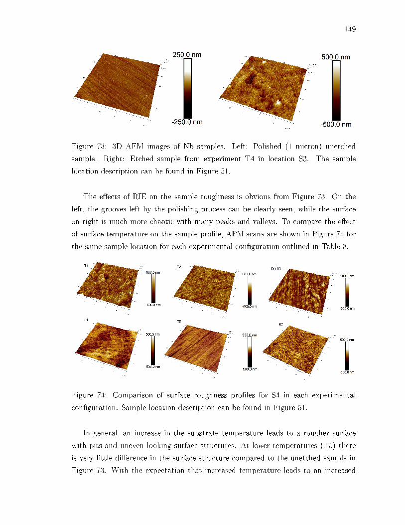
149
Figure 73: 3D AFM images of Nb samples. Left: Polished (1 micron) unetched
sample. Right: Etched sample from experiment T4 in location S3. The sample
location description can be found in Figure 51.
The eects of RIE on the sample roughness is obvious from Figure 73. On the
left, the grooves left by the polishing process can be clearly seen, while the surface
on right is much more chaotic with many peaks and valleys. To compare the eect
of surface temperature on the sample prole, AFM scans are shown in Figure 74 for
the same sample location for each experimental conguration outlined in Table 8.
Figure 74: Comparison of surface roughness proles for S4 in each experimental
conguration. Sample location description can be found in Figure 51.
In general, an increase in the substrate temperature leads to a rougher surface
with pits and uneven looking surface structures. At lower temperatures (T5) there
is very little dierence in the surface structure compared to the unetched sample in
Figure 73. With the expectation that increased temperature leads to an increased

150
etch rate, this general trend is not surprising. Furthermore, the temperature for
this particular sample is ≈ 200 oC, whereas the boiling point of NbCl5, the desired
volatile product, is 250 oC. Thus, we would not expect much etching of this sample
and indeed the etch rate was among the smallest at 7.15 nm/min. In the same
vein, an increase in the DC bias (B2) shows an even further increase in the pit-like
structure. This is likely due to the increased physical etching aided by the higher bias
potential, and therefore a higher ion energy. Further verication of this hypothesis
can be seen in Figure 75, which corresponds to sample 1 in experiment B2.
Figure 75: AFM scan of S1 in conguration B2. This sample was found to have a
negligible etch rate. The sample location description can be found in Figure 51.
This is a particularly interesting example as the etch rate was measured to be
approximately 0, even though the surface temperature should have been sucient
for chemical etching. Regardless, one can see that with minimal to no chemical
etching, the surface still shows signicant pitting and uneven characteristics that are
indicative of purely physical, sputtering type interactions.
9.3.2 RMS SURFACE ROUGHNESS

151
The RMS surface roughness for each sample is presented in Table 9 and in Figure
76.
400 500 600 700 400 500 600 700 400 500 600 700 400 500 600 700 800
S1 S2 S3 S4
0
25
50
75
100
125
150
175
200
RM
S R
ough
ness
(nm
)
Temperature (K)
T1 T2 T3 T4 T5 B2
Figure 76: RMS surface roughness vs. surface temperature for each sample position.
The raw data and identier can be found in Table 9. Data is presented without error
bars for clarity.
Interestingly, there is no discernible connection between the substrate tempera-
ture and the RMS surface roughness. The same can be said in regards to the sample
position as no trend appears to exist. The eects of temperature and DC bias dis-
cussed in the previous section seem to only apply at very small scales, rather than a
macroscopically.
It is important at this point to compare the RMS surface roughness of the plasma
etched Nb samples to the typical surface roughness of traditional cavity processing

152
Table 9: RMS results for each sample and experimental conguration. In all cases,
the scan area was 50 µm × 50 µm. There were two polished and unetched samples
with RMS roughness < 30 nm.
Identier Sample T (K) RMS Roughness (nm)
T1
S1 645 ± 10.25 91.35
S2 471 ± 7.56 110.00
S3 667 ± 10.40 343.00
S4 625 ± 0.82 139.00
T2
S1 609 ± 2.20 44.95
S2 493 ± 6.30 48.80
S3 590 ± 6.96 50.45
S4 576 ± 0.90 44.95
T3/B1
S1 517 ± 12.04 34.75
S2 525 ± 1.54 59.85
S3 500 ± 7.00 103.90
S4 468 ± 5.18 68.90
T4
S1 659 ± 11.19 66.65
S2 681 ± 2.69 91.55
S3 640 ± 7.59 37.40
S4 588 ± 4.18 109.00
T5
S1 455 ± 7.78 74.40
S2 422 ± 3.42 76.40
S3 484 ± 2.15 58.05
S4 475 ± 4.50 37.00
B2
S1 536 ± 4.81 30.80
S2 493 ± 3.28 99.75
S3 594 ± 1.08 144.50
S4 537 ± 4.56 70.90

153
techniques. The typical resulting RMS surface roughness for the Buered Chemical
Polished (BCP) chemical process is about 1.6 ± 0.42 µm [100], while Electropolishing
(EP) can achieve better results with a typical value of about 0.34 ± 0.11 µm [101]
for a 50 µm × 50 µm scan area [102]. As seen in Table 9, the highest RMS surface
roughness is ≈ 150 nm. Additionally, these samples did not undergo any additional
processing or cleaning other than simple hand cleaning with methanol and isopropyl
alcohol. These results are certainly promising, but the inhomogeneity of the nal
sample surface is a concern.
9.3.3 SURFACE COMPOSITION AND IMPURITIES
The experimental requirements for RIE of the inner surface of a cylindrical surface
inherently introduces the samples to potential impurities through the experimental
components. Ideally, all of these individual pieces would be made of specialized
highly corrosive resistant materials, but this is monetarily infeasible, especially for
a developmental technology still in its adolescence. Therefore, the introduction of
foreign impurities on the surface of the samples is inevitable, especially with the
necessary use of chlorine for the RIE process. However, identifying the source and
amount of impurities as they are related to the experimental parameters can aid in
the development of tactics for their mitigation. In this aim, the Phenom SEM is
particularly useful as atomic and weight concentrations of elements on a material
surface can be explicitly measured. The most signicant sources of experimentally
detrimental impurities and suggestions for their reduction are outlined in this section.
In the case of this particular experiment, the most obvious source of impurities
is carbon, which can be embedded into the surface from the polishing process. To
a lesser extent, trace amounts of silicon can be found in some instances due to the
berglass insulation on the thermocouple wires. Additionally, etching of the stainless
steel components of the chamber can occur, especially at higher temperatures and Cl2
concentrations. These impurities have indeed caused issues in previous works [1, 38]
and eorts were made to reduce them by constructing the gas and power delivery
components out of niobium or nickel based alloys as they are constantly exposed to
the reactive discharge (see Section 6.1). The complete elimination of stainless steel
in the system is impractical as it is the standard material used in the production of
commercial vacuum chamber components. However, the material change of the gas
and power greatly reduced the amount of impurities as a whole.

154
Certainly an increased temperature can help alleviate these issues in some cases
as the impurities would remain volatile enough to be pumped out of the system.
However, the temperatures of the system, particularly when the chamber is heated
further from the outside to increase the substrate temperature, can facilitate reactions
with the stainless steel chamber walls and the copper gaskets used for the vacuum
seal. Indeed, impurities related to these materials were found on local regions of
samples in the T1 conguration as seen in Figure 77.
Figure 77: Material spectrum, spot image, and composition table for sample 1 in the
T1 experimental conguration. The location corresponding to the material spectrum
is circled in blue. Conguration information can be found in Table 9 and sample
location description can be found in Figure 51.
It seems that this is the rst instance of the formation of Cu impurities in any
of the related RIE studies at Old Dominion University. This is due to the high tem-
peratures used in this experiment (T1 in particular) compared to the previous work
as discussed in Section 9.2.1 [1]. It seems that the temperature was high enough to
create copper chlorides, which were quickly deposited on the surfaces of the appa-
ratus. Additionally, chromium from the stainless steel parts, and more specically
the nuts used to compression t the thermocouples (see Figure 50), reacted with
chlorine to make chromic chloride (CrCl3) which is discernible by its distinct purple
color. In addition, the Nb conical gas inlet (shown in Figure 32) was destroyed during
the etching experiment. This gas feed was used throughout the studies outlined in
Chapters 7 and 8 which used comparable experimental conditions with the exception
of the surface temperature. The higher surface roughness of the samples in the T1

155
experiment are attributed to these eects. Thus, it was necessary to explore possible
options to eliminate the production of copper impurities and the destruction of the
gas feed components.
The commercially available replacements for Cu gaskets include silver, gold, and
nickel. Among these, only nickel can withstand the combination of high tempera-
tures and corrosiveness of Cl2. As the price of the solid Ni gaskets were exorbitant
(roughly 48 times more expensive per gasket) we elected to instead have Cu gaskets
electrolytically Ni plated by a local metal plating business. It was expected that these
would work in the same manner as the solid Ni gaskets as the only requirements were
that no copper was exposed and sucient vacuum can be achieved. This study was
conducted in tandem with the surface roughness and etch rate experiments to utilize
the SEM measurements and see the eects of these material changes on these surface
studies. In addition, the destruction of the gas feed led to the development of the
laminar showerhead gas inlet shown in Figures 33 and 34. The laminar showerhead
was constructed of a nickel alloy (InconelTM 600) that has particularly high corrosion
resistance. The dierent gasket material and gas feed congurations are listed in
Table 10 for each sample experiment.
Table 10: Gasket material and gas feed conguration for each sample experiment.
Identier Gasket Material/Gas Feed Conguration
T1 Conical niobium gas feed (destroyed). Copper gaskets only.
T2 No gas feed. Single 6" Ni plated gasket in reaction region.
T3/B1 No gas feed. All Ni plated gaskets for chamber components.
T4 No gas feed. All Ni plated gaskets for chamber components.
T5 Laminar ow gas feed. Two 6" Ni plated gaskets in reaction region.
B2 Laminar ow gas feed. Two 6" Ni plated gaskets in reaction region.
The `reaction region' in Table 10 refers to the gaskets located on either side of the
cavity structure shown in Figures 29 and 31. There are a couple of general comments
that can be made for all of the samples for experiments T2-5 and B2. In all samples,
even those that were not plasma etched, there exists a small fraction of phosphorus on
the surface. The inclusion of this element on the sample surface is puzzling and there
is no known reason for its existence. However it is possible that the SEM is mistaking
an artifact of the Nb peak in the spectrum as P. Regardless, the concentration of P

156
is ignored when considering the surface concentration of impurities. Secondly, there
are no measured traces of Cu on any sample in any of these congurations. This
is an encouraging development as the use of nickel or nickel plated pieces could be
an eective, experimentally feasible, and relatively inexpensive method of preventing
Cu and other stainless steel impurities. It is evident that at these high temperatures
it is imperative that durable anti-corrosive materials be used when possible to reduce
byproducts and increase the longevity of the apparatus.
In terms of impurity concentration, carbon is by far the most abundant across
all samples and experimental congurations. The amount of carbon has a large
variation in general, but it seems that samples at lower temperatures retain higher
amounts of carbon impurities, which is not particularly surprising. The second high-
est would be nickel impurities, which were almost explicitly located on samples 2 and
3. Other impurities include Cr, Fe, and trace amounts of Si which are all typically
found indiscriminately in small amounts. Examples of surface locations with high
concentrations of impurities can be seen in Figure 78.
Figure 78: Left: Example of a location with high carbon deposit (C: 38.83%). Right:
Example of a location with high stainless steel impurity deposits (Ni: 59.06 % Cr:
2.13 % Fe: 0.92 %).
It is evident that the reduction of chemical byproducts and embedded impurities
through improved material design, uniform cavity heating, and the development of an

157
in situ cleaning process are some of the most signicant limitations of this technology
at its present state, and therefore require further study.
Relative Nb and O Concentration
Niobium naturally oxidizes instantaneously due to the large bonding energy be-
tween the Nb and O atoms [22]. For the purposes of superconductivity, the metallic
interface has a thin NbO layer that acts as a protective barrier for the superconduct-
ing bulk Nb below the surface. However, the oxidation is often dominated by the
production of crystalline Nb2O5 which creates strains and basically `eats' into the
bulk Nb [22, 103]. Measuring the relative concentration between Nb and O on the
surface can indicate whether the surface is composed of NbO or Nb2O5. The atomic
masses of Nb and O are 41 and 8 amu, respectively, so an atomic concentration of
67 % Nb and 33 % O is indicative of a Nb2O5 surface layer.
The vast majority of the samples indeed show atomic concentrations that are
indicative of a Nb2O5 surface layer. However, there are cases in which a higher Nb
concentration is seen in a macroscopic region, or a higher O concentration is seen in
a macroscopic region. Examples of two such regions are shown in Figure 79.
Figure 79: Left: Example of a region scan with high Nb concentration (Nb: 71.94 %
O: 24.06 %). Right: Example of a region scan with high O concentration (O: 62.14
% Nb: 35.08 %).

158
The dierence in surface structures can be seen clearly as the O heavy sample
region has a great deal of blemishes. According to corresponding spot scans (not
pictured) the darker regions around the blemishes are local areas of high relative
O. As these two particular cases are exceptions, further study is required to fully
understand how these surfaces came to be.
9.4 SUMMARY
Experiments were conducted on small Nb coupon samples to study the eect of
the substrate surface temperature and driven electrode DC bias on their respective
etch rate and surface roughness proles. Four samples were etched simultaneously
for each set of external parameters at dierent locations within the chamber corre-
sponding to dierent local regions of the discharge. As a function of temperature,
the etch rates of samples corresponding to the same location show an Arrhenius type
dependence that corresponds to a strong chemical etching component of the pro-
cess. This conrms previous measurements and observations by Upadhyay [1] where
a similar relationship was found, although with a lower activation energy. At similar
temperatures, an increase in the positive DC bias seems to increase the etch rate,
but more data is required in order to substantiate this claim.
The surface roughness of each sample was measured using an atomic force micro-
scope (AFM) for each sample. The AFM is capable of producing 2D and 3D images
of the surface prole, while also providing the RMS surface roughness in a specic
scan region. While an increase in temperature seems to cause pit-like defects on the
surface based on qualitative observations of the images, the RMS surface results show
no direct correlation between the two parameters. An increase in the positive DC
bias also seems to modify the surface to a more `bumpy' structure indicative of an
increase in the physical sputtering of the sample, but once again the RMS roughness
shows no correlation between the two parameters.
A scanning electron microscope (SEM) was used to provide high denition optical
images of the surface and measure the atomic composition of the surface. The nature
of the experiment introduces a great deal of potential surface impurities that could be
detrimental to the surface characteristics and superconducting properties of Nb. The
SEM is used to investigate the sources of surface impurities that are embedded during
plasma etching under various conditions. The intention is to use this information to
develop material and engineering solutions for the mitigation of these problematic

159
impurities. Among the most signicant source of impurities are the copper gaskets
that are used to seal the vacuum chamber, particularly at high temperatures. The
solution to this issue was to plate the gaskets with nickel as it has a much higher
threshold for corrosive reactions. The gaskets can be plated and implemented with
no concerns for the sealing eectiveness, while copper impurities were completely
avoided. It is suggested that this also be applied to a great deal of the other vacuum
components used for the plasma etch process as stainless steel impurities can be
problematic, and nickel plating is a relatively straightforward and cheap process,
especially compared to the production of the same pieces using solid nickel.
Due to the highly destructive nature of the discharge at high temperatures the
conical gas feed delivery system was destroyed in the rst sample etching experi-
ment. Therefore, a replacement gas feed was designed and produced with particular
considerations given to the material and uniform gas delivery. The nal product was
a laminar ow showerhead made of highly corrosive resistant nickel alloys. While
quantitative comparisons cannot be made at this time, it is the opinion of the author
that this design is far superior to the previous design in both longevity and uniform
gas delivery considerations.

160
CHAPTER 10
CONCLUSION
This dissertation presents work that is a continuation of the development of a
Reactive Ion Etching (RIE) technology for the processing of superconducting radio-
frequency (SRF) cavities. Reactive Ion Etching, or plasma etching, is a dry etch
process that could serve as a benecial addition to or possible replacement of the
current wet etch cavity processing routines. The previous work on this front estab-
lished empirical relationships between the user controlled external parameters and
the removal of surface layers of the niobium cavity. However, missing from that
study, and a focus of this one, is the connection of these external etching parameters
to the physical description of the plasma. The measurement and understanding of
these plasma parameters are particularly important for the future of the technology.
A more complete understanding of the process at large would allow for the develop-
ment of computer jelly models that aid in the physical description of the etching
system as a whole. A computer model, in conjunction with the experimental results
herein, would aid in the development of an eective and controllable etching routine.
In order to etch the inner surface of a cavity, the plasma must be created within
the cavity, meaning that a powered electrode must be placed in the center. This
type of conguration creates a coaxial plasma instead of a at parallel plate plasma
commonly used in industrial applications. This oers the opportunity to study the
physics of a plasma conguration of which very little is known.
The plasma parameters of particular interest for this work include the densities
of the rst four excited states of Argon (1s states in Paschen notation), the electron
density (ne), and the electron temperature (Te) in both Argon and Ar/Cl2 plasmas.
The 1s states of Argon are useful as they are involved in a majority of the higher
energy (>10 eV) excitation and radiative decay processes, as well as ionization from
collisions of excited atoms. Additionally, there exist a large array of spectral lines
that correspond to transitions from the next ten excited levels of Argon (2p levels
in Paschen notation) that are easily measurable with basic spectroscopic equipment.
Information about the signicant kinetic processes of these excited states can be
measured from these transitions and applied to a collisional radiative model (CRM)

161
to nd information about the distribution of electrons in the respective discharge.
Electrons are the primary source of energy transfer in the discharge due to their high
mobility in the oscillating electric elds. Electrons provide energy to the Ar and Cl
atoms through collisions causing ionization and excitation. Thus, knowledge of ne
and the average electron energy Te as functions of the external is imperative for the
development of a consistent discharge model.
The densities of the rst four excited states in Argon were measured using two
distinctly dierent optical spectroscopy techniques. These excited state densities
were measured for both Ar and Ar/Cl2 mixtures of varying concentrations as the
Ar/Cl2 mixture is necessary for etching of SRF cavities. The two measurement
techniques, tunable diode laser absorption spectroscopy (TDLAS) and the optical
emission spectroscopy branching fraction method (OES-BFM), were conducted as
pertinent external parameters were varied to develop a working model to describe
the discharge. TDLAS is used to measure the Doppler broadened prole of a spectral
line by sweeping a tunable diode laser across the resonant frequency of the transition.
The absorption prole is representative in the velocity distribution of the absorbing
species, and can be used to calculate the population density. OES-BFM uses the
relationship between the optical emission of spectral lines and the density of the nal
state. In particular, the connection between the resonant reabsorption of photons
traveling through the plasma and the absorbing species is utilized, therefore circum-
venting the need for any a priori knowledge of the energy distribution. As a direct
comparison, TDLAS is much more eective than OES-BFM at measuring the excited
state densities with accuracy and consistency, while OES-BFM has the signicant
advantage of being a more robust method capable of measuring all four excited states
simultaneously. The results of this work show agreement between the two methods
up to a factor of three for the vast majority of the external parameters studied.
The results from the optical spectroscopy studies were then applied to a collisional
radiative model (CRM) to calculate pertinent information about the electron energy
and density in the discharge. The CRM uses the balancing of the population and
depopulation processes of excited states (2p levels of Argon in this case) to calculate
unknown quantities involved in the transitions. In this case, the 1s state densities
are among the major population channels of the 2p levels, and their densities mea-
sured from the diagnostic methods can be used to nd the electron temperature and
density. Additionally, an alternative method found in the literature for calculating

162
the electron density using the ratio of the 1s5 metastable level and 1s4 resonant level
was explored. We have established signicant relationships between the etching and
plasma parameters that are very useful for the future design of computer jelly mod-
els" and etching experiments. Among the most surprising and exciting results is
the magnitude of the electron density which is in the order of 1018 m−3. Densities
of these magnitudes are not typically found in capacitively coupled discharges and
require higher power or magnetic sources. This fact alone suggests that the simple
geometrical change from typical parallel plate to coaxial congurations could pro-
vide the same benets for etching processes that would normally require a signicant
increase in power.
As an extension to the etching studies performed in previous works, the eect of
RIE on the nal surface structure of niobium was studied. The surface roughness
and composition of bulk niobium is directly related to its inherent superconducting
properties. In this aim niobium coupon samples were plasma etched to study the
eects of substrate temperature and the driven electrode DC bias on the nal surface
as these are understood to be directly related to the chemical and physical etching
components, respectively. Four samples were etched simultaneously for each set of
external parameters at dierent locations within the chamber corresponding to dif-
ferent local regions of the discharge. An atomic force microscope (AFM) was used
to measure the surface roughness characteristics of each sample, while a scanning
electron microscope (SEM) was used to measure the surface composition. In gen-
eral, plasma etched niobium samples show an RMS surface roughness lower than the
standard wet chemical etch processes typical of cavity processing. The experimen-
tal requirements of this plasma etch process forces the introduction of the etching
substrate to potential impurities that may arise from the experimental chamber, par-
ticularly when corrosive halogen gases are used. The SEM measurements were used
to help identify and eliminate signicant sources of impurities related to the con-
struction of the apparatus. It was found that using nickel and nickel alloys provide
signicant benets in the reduction of detrimental impurities that would otherwise
be unavoidable.
To conclude, we have measured the plasma parameters as a function of external
etching parameters of a cylindrical coaxial capacitively coupled plasma designed for
the processing of Nb SRF cavities. The plasma parameters are important inputs
for computational models that can more eectively model the discharge chamber

163
as a whole. Surface properties and roughness proles were studied as functions of
parameters that pertain to the etching mechanisms of the Ar/Cl2 plasma. Basic
relationships between the external parameters and the etch rate, surface roughness,
and impurity deposition have been established. These investigations were the next
logical steps in the advancement of RIE technology for the processing of Nb SRF
cavities and provide a framework for the establishment of eective, consistent, and
controllable plasma etching routines that could signicantly improve the operation
of superconducting particle accelerators around the world.

164
REFERENCES
[1] Janardan Upadhyay. Plasma Processing of Superconducting Radio Frequency
Cavities. PhD thesis, Old Dominion University, 2016.
[2] Allan J. Lichtenberg Michael A. Lieberman. Principles of Plasma Discharges
and Materials Precessing. John Wiley & Sons Inc., 1994.
[3] A von Keudell and V Schulz von der Gathen. Foundations of low-temperature
plasma physicsan introduction. Plasma Sources Science and Technology, 26
(11):113001, oct 2017.
[4] M Nikolic. Characterization of Microwave Discharge Plasmas for Surface Pro-
cessing. PhD thesis, Old Dominion University, 2013.
[5] H. R. Koenig and L. I. Maissel. Application of rf discharges to sputtering. IBM
Journal of Research and Development, 14(2):168171, March 1970.
[6] Janardan Upadhyay, Svetozar Popovi¢, Leposova Vuskovi¢, Do Im, Anne-Marie
Valente, and H Phillips. Plasma processing of large surfaces with application
to srf cavity modication. Technical report, Thomas Jeerson National Accel-
erator Facility, Newport News, VA (United States), 2013.
[7] Janardan Upadhyay, Do Im, S Popovi¢, A-M Valente-Feliciano, L Phillips, and
L Vuskovi¢. Etching mechanism of niobium in coaxial ar/cl2 radio frequency
plasma. Journal of Applied Physics, 117(11):113301, 2015.
[8] Janardan Upadhyay, Do Im, Svetozar Popovi¢, Leposava Vuskovi¢, Anne-Marie
Valente-Feliciano, and Larry Phillips. Reversal of the asymmetry in a cylindri-
cal coaxial capacitively coupled ar/cl2 plasma. Journal of Vacuum Science &
Technology A: Vacuum, Surfaces, and Films, 33(6):061309, 2015.
[9] J. Upadhyay, J. Peshl, S. Popovi¢, A.-M. Valente-Feliciano, and L. Vuskovi¢.
Eect of self-bias on cylindrical capacitive discharge for processing of inner
walls of tubular structurescase of srf cavities. AIP Advances, 8(8):085008,
2018.
[10] V. A. Godyak, R. B. Piejak, and B. M. Alexandrovich. Probe diagnostics of
non-maxwellian plasmas. Journal of Applied Physics, 73(8):36573663, 1993.

165
[11] John B Board, RO Jung, Chun C Lin, and AE Wendt. Optical emission
measurements of electron energy distributions in low-pressure argon inductively
coupled plasmas. Plasma Sources Science and Technology, 19(6):065001, 2010.
[12] J T Gudmundsson. On the eect of the electron energy distribution on the
plasma parameters of an argon discharge: a global (volume-averaged) model
study. Plasma Sources Science and Technology, 10(1):7681, jan 2001.
[13] M. J. Druyvesteyn and F. M. Penning. The mechanism of electrical discharges
in gases of low pressure. Rev. Mod. Phys., 12:87174, Apr 1940.
[14] John B Board, Garrett A Piech, Mark F Gehrke, LW Anderson, and Chun C
Lin. Measurement of electron-impact excitation cross sections out of metastable
levels of argon and comparison with ground-state excitation. Physical Review
A, 59(4):2749, 1999.
[15] John B Board, Chun C Lin, and Charles A DeJoseph Jr. Application of
excitation cross sections to optical plasma diagnostics. Journal of Physics D:
Applied Physics, 37(12):R143, 2004.
[16] John B Board, B Chiaro, Tobin Weber, and Chun C Lin. Electron-impact
excitation of argon: Optical emission cross sections in the range of 3002500
nm. Atomic Data and Nuclear Data Tables, 93(6):831863, 2007.
[17] John B Board, RO Jung, LW Anderson, and CC Lin. Electron-impact exci-
tation of rare-gas atoms from the ground level and metastable levels. Advances
in Atomic Molecular and Optical Physics, 54:320, 2007.
[18] J Ethan Chilton, John B Board, R Scott Schappe, and Chun C Lin. Mea-
surement of electron-impact excitation into the 3 p 5 4 p levels of argon using
fourier-transform spectroscopy. Physical Review A, 57(1):267, 1998.
[19] O Zatsarinny and K Bartschat. B-spline breitpauli r-matrix calculations for
electron collisions with argon atoms. Journal of Physics B: Atomic, Molecular
and Optical Physics, 37(23):46934706, nov 2004.
[20] Oleg Zatsarinny, Yang Wang, and Klaus Bartschat. Electron-impact excitation
of argon at intermediate energies. Phys. Rev. A, 89:022706, Feb 2014.

166
[21] Arati Dasgupta, M Blaha, and JL Giuliani. Electron-impact excitation from
the ground and the metastable levels of ar i. Physical review A, 61(1):012703,
1999.
[22] Gianluigi Ciovati. Investigation Of The Superconducting Properties Of Niobium
Radio-Frequency Cavities. PhD thesis, Old Dominion University, 2005.
[23] Hasan S Padamsee. Superconducting radio-frequency cavities. Annual review
of nuclear and particle science, 64:175196, 2014.
[24] B. Aune, R. Bandelmann, D. Bloess, B. Bonin, A. Bosotti, M. Champion,
C. Crawford, G. Deppe, B. Dwersteg, D. A. Edwards, H. T. Edwards, M. Fer-
rario, M. Fouaidy, P.-D. Gall, A. Gamp, A. Gössel, J. Graber, D. Hu-
bert, M. Hüning, M. Juillard, T. Junquera, H. Kaiser, G. Kreps, M. Kuch-
nir, R. Lange, M. Leenen, M. Liepe, L. Lilje, A. Matheisen, W.-D. Möller,
A. Mosnier, H. Padamsee, C. Pagani, M. Pekeler, H.-B. Peters, O. Peters,
D. Proch, K. Rehlich, D. Reschke, H. Safa, T. Schilcher, P. Schmüser, J. Seku-
towicz, S. Simrock, W. Singer, M. Tigner, D. Trines, K. Twarowski, G. We-
ichert, J. Weisend, J. Wojtkiewicz, S. Wol, and K. Zapfe. Superconducting
tesla cavities. Phys. Rev. ST Accel. Beams, 3:092001, Sep 2000.
[25] Walther Meissner and Robert Ochsenfeld. Ein neuer eekt bei eintritt der
supraleitfähigkeit. Naturwissenschaften, 21(44):787788, 1933.
[26] Heike Kamerligh-Onnes. The superconductivity of mercury. Comm. Phys. Lab.
Univ. Leiden, 122:122124, 1911.
[27] C Jo Gorter and HBG Casimir. The thermodynamics of the superconducting
state. Z. tech. Phys, 15:53942, 1934.
[28] Fritz London and Heinz London. The electromagnetic equations of the supra-
conductor. Proceedings of the Royal Society of London. Series A-Mathematical
and Physical Sciences, 149(866):7188, 1935.
[29] Alfred Brian Pippard and William Lawrence Bragg. An experimental and
theoretical study of the relation between magnetic eld and current in a super-
conductor. Proceedings of the Royal Society of London. Series A. Mathematical
and Physical Sciences, 216(1127):547568, 1953.

167
[30] VL Ginzburg and LD Landau. Phenomenological theory. J. Exp. Theor. Phys.
USSR, 20:1064, 1950.
[31] A. Gurevich. Nonlocal josephson electrodynamics and pinning in superconduc-
tors. Phys. Rev. B, 46:31873190, Aug 1992.
[32] John Bardeen, Leon N Cooper, and John Robert Schrieer. Theory of super-
conductivity. Physical review, 108(5):1175, 1957.
[33] Hasan Padamsee, Jens Knobloch, Tom Hays, et al. RF superconductivity for
accelerators, volume 2011. Wiley Online Library, 2008.
[34] Ralph Howard Fowler and Lothar Nordheim. Electron emission in intense
electric elds. Proceedings of the Royal Society of London. Series A, Containing
Papers of a Mathematical and Physical Character, 119(781):173181, 1928.
[35] Ari Palczewski. R & d progress in srf surface preparation with centrifugal
barrel polishing (cbp) for both nb and cu. Technical report, Thomas Jeerson
National Accelerator Facility, Newport News, VA (United States), 2013.
[36] J Upadhyay, Do Im, S Popovi¢, A-M Valente-Feliciano, L Phillips, and
L Vuskovi¢. Plasma processing of large curved surfaces for superconducting rf
cavity modication. Physical Review Special Topics-Accelerators and Beams,
17(12):122001, 2014.
[37] Janardan Upadhyay, Do Im, J Peshl, M Basovi¢, S Popovi¢, A-M Valente-
Feliciano, L Phillips, and Leposova Vuskovi¢. Apparatus and method for plasma
processing of srf cavities. Nuclear Instruments and Methods in Physics Research
Section A: Accelerators, Spectrometers, Detectors and Associated Equipment,
818:7681, 2016.
[38] J Upadhyay, A Palczewski, S Popovi¢, A-M Valente-Feliciano, Do Im,
HL Phillips, and L Vuskovi¢. Cryogenic rf test of the rst srf cavity etched
in an rf ar/cl2 plasma. AIP Advances, 7(12):125016, 2017.
[39] M. A. Lieberman and S. E. Savas. Bias voltage in nite length, cylindrical and
coaxial radio frequency discharges. Journal of Vacuum Science & Technology
A, 8(3):16321641, 1990.
168
[40] E. Kawamura, M. A. Lieberman, A. J. Lichtenberg, and E. A. Hudson. Capac-
itive discharges driven by combined dc/rf sources. Journal of Vacuum Science
& Technology A, 25(5):14561474, 2007.
[41] E Kawamura, A J Lichtenberg, and M A Lieberman. Secondary electrons in
rf and dc/rf capacitive discharges. Plasma Sources Science and Technology, 17
(4):045002, aug 2008.
[42] Wei Jiang, Xiang Xu, Zhong-Ling Dai, and You-Nian Wang. Heating mech-
anisms and particle ow balancing of capacitively coupled plasmas driven by
combined dc/rf sources. Physics of Plasmas, 15(3):033502, 2008.
[43] Vincent M Donnelly and Avinoam Kornblit. Plasma etching: Yesterday, today,
and tomorrow. Journal of Vacuum Science & Technology A: Vacuum, Surfaces,
and Films, 31(5):050825, 2013.
[44] M Ra²kovi¢, J Upadhyay, L Vu²kovi¢, S Popovi¢, AM Valente-Feliciano, and
L Phillips. Plasma treatment of bulk niobium surface for superconducting rf
cavities: Optimization of the experimental conditions on at samples. Physical
Review Special Topics-Accelerators and Beams, 13(11):112001, 2010.
[45] CJ Mogab. The loading eect in plasma etching. Journal of the Electrochemical
Society, 124(8):12621268, 1977.
[46] VM Donnelly, DL Flamm, CW Tu, and DE Ibbotson. Temperature dependence
of inp and gaas etching in a chlorine plasma. Journal of The Electrochemical
Society, 129(11):25332537, 1982.
[47] SJ Pearton, AB Emerson, UK Chakrabarti, E Lane, KS Jones, KT Short,
Alice E White, and TR Fullowan. Temperature dependence of reactive ion
etching of gaas with ccl2f2: O2. Journal of Applied Physics, 66(8):38393849,
1989.
[48] H. M. Mott-Smith and Irving Langmuir. The theory of collectors in gaseous
discharges. Phys. Rev., 28:727763, Oct 1926.
[49] VA Godyak and VI Demidov. Probe measurements of electron-energy distri-
butions in plasmas: what can we measure and how can we achieve reliable
results? Journal of Physics D: Applied Physics, 44(23):233001, 2011.

169
[50] Francis F. Chen. Langmuir probe analysis for high density plasmas. Physics
of Plasmas, 8(6):30293041, 2001.
[51] J E Allen, R L F Boyd, and P Reynolds. The collection of positive ions by a
probe immersed in a plasma. Proceedings of the Physical Society. Section B,
70(3):297304, mar 1957.
[52] Bernstein Ira B. and Rabinowitz Irving N. Theory of electrostatic probes in a
low density plasma. The Physics of Fluids, 2(2):112121, 1959.
[53] M. J. Druyvesteyn. Der niedervoltbogen. Zeitschrift für Physik, 64(11):781
798, Sep 1930.
[54] Nancy L. Bassett and Demetre J. Economou. Eect of cl2 additions to an
argon glow discharge. Journal of Applied Physics, 75(4):19311939, 1994.
[55] Ramamurti Shankar. Principles of quantum mechanics. Springer Science &
Business Media, 2012.
[56] A. Kramida, Yu. Ralchenko, J. Reader, and and NIST ASD Team.
NIST Atomic Spectra Database (ver. 5.6.1), [Online]. Available:
https://physics.nist.gov/asd [2019, May 31]. National Institute of
Standards and Technology, Gaithersburg, MD., 2018.
[57] M Schulze, A Yanguas-Gil, A von Keudell, and P Awakowicz. A robust method
to measure metastable and resonant state densities from emission spectra in
argon and argon-diluted low pressure plasmas. Journal of Physics D: Applied
Physics, 41(6):065206, feb 2008.
[58] John B Board, RO Jung, Chun C Lin, and AE Wendt. Measurement of
metastable and resonance level densities in rare-gas plasmas by optical emission
spectroscopy. Plasma Sources Science and Technology, 18(3):035017, 2009.
[59] V. P. Sushkov, H. T. Do, and R. Hippler. Application of the escape factor
method for determination of excited states densities in a low-pressure argon
radio-frequency discharge. Contributions to Plasma Physics, 53(7):549559,
2013.

170
[60] Marcel Fiebrandt, Bastian Hillebrand, Stefan Spiekermeier, Nikita Bibinov,
Marc Böke, and Peter Awakowicz. Measurement of ar resonance and metastable
level number densities in argon containing plasmas. Journal of Physics D:
Applied Physics, 50(35):355202, aug 2017.
[61] Jiang Li, Fei-Xiang Liu, Xi-Ming Zhu, and Yi-Kang Pu. The spatially resolved
measurements of the atomic densities in argon paschen 1s levels by OES in a
capacitively coupled plasma. Journal of Physics D: Applied Physics, 44(29):
292001, jul 2011.
[62] T. Holstein. Imprisonment of resonance radiation in gases. Phys. Rev., 72:
12121233, Dec 1947.
[63] R.W.P. McWhirter. In R. H. Huddlestone and S. L. Leonard, editors, Plasma
Diagnostic Techniques, page 201, 1965.
[64] Yu Golubovskii, S Gorchakov, and D Uhrlandt. Transport mechanisms of
metastable and resonance atoms in a gas discharge plasma. Plasma Sources
Science and Technology, 22(2):023001, feb 2013.
[65] Xi-Ming Zhu, Zhi-Wen Cheng, Yi-Kang Pu, and Uwe Czarnetzki. Escape
factors for paschen 2p1s emission lines in low-temperature ar, kr, and xe
plasmas. Journal of Physics D: Applied Physics, 49(22):225204, may 2016.
[66] R Mewe. Relative intensity of helium spectral lines as a function of electron
temperature and density. British Journal of Applied Physics, 18(1):107118,
jan 1967.
[67] R. Mewe. Simplied model for ionization and recombination in a hydrogenic
plasma with resonance radiation trapping. Zeitschrift für Naturforschung A,
25(12), 1970.
[68] Xi-Ming Zhu, Zhi-Wen Cheng, Emile Carbone, Yi-Kang Pu, and Uwe Czarnet-
zki. Determination of state-to-state electron-impact rate coecients between
ar excited states: a review of combined diagnostic experiments in afterglow
plasmas. Plasma Sources Science and Technology, 25(4):043003, jul 2016.
[69] Xi-Ming Zhu and Yi-Kang Pu. A simple collisionalradiative model for low-
temperature argon discharges with pressure ranging from 1pa to atmospheric

171
pressure: kinetics of paschen 1s and 2p levels. Journal of Physics D: Applied
Physics, 43(1):015204, dec 2009.
[70] J T Gudmundsson and E G Thorsteinsson. Oxygen discharges diluted with
argon: dissociation processes. Plasma Sources Science and Technology, 16(2):
399412, apr 2007.
[71] Chun C Lin. Measurements of electron-impact excitation cross sections out
of the ground and metastable levels of rare gases with applications to low-
temperature plasmas. Contributions to Plasma Physics, 44(5-6):405412, 2004.
[72] J Vlcek. A collisional-radiative model applicable to argon discharges over a
wide range of conditions. i. formulation and basic data. Journal of Physics D:
Applied Physics, 22(5):623631, may 1989.
[73] M C Bordage, S F Biagi, L L Alves, K Bartschat, S Chowdhury, L C Pitchford,
G J M Hagelaar, W L Morgan, V Puech, and O Zatsarinny. Comparisons of
sets of electronneutral scattering cross sections and swarm parameters in noble
gases: III. krypton and xenon. Journal of Physics D: Applied Physics, 46(33):
334003, aug 2013.
[74] Sarah Siepa, Stephan Danko, Tsanko V Tsankov, Thomas Mussenbrock, and
Uwe Czarnetzki. On the oes line-ratio technique in argon and argon-containing
plasmas. Journal of Physics D: Applied Physics, 47(44):445201, 2014.
[75] Xi-Ming Zhu, Tsanko Vaskov Tsankov, Dirk Luggenhölscher, and Uwe Czar-
netzki. 2d collisional-radiative model for non-uniform argon plasmas: with or
without `escape factor'. Journal of Physics D: Applied Physics, 48(8):085201,
feb 2015.
[76] Xi-Ming Zhu and Yi-Kang Pu. Optical emission spectroscopy in low-
temperature plasmas containing argon and nitrogen: determination of the elec-
tron temperature and density by the line-ratio method. Journal of Physics D:
Applied Physics, 43(40):403001, sep 2010.
[77] Shicong Wang, Amy E. Wendt, John B. Board, Chun C. Lin, Svetlana
Radovanov, and Harold Persing. Noninvasive, real-time measurements of
plasma parameters via optical emission spectroscopy. Journal of Vacuum Sci-
ence & Technology A, 31(2):021303, 2013.

172
[78] John B Board, RO Jung, Chun C Lin, LE Aneskavich, and AE Wendt. Ar-
gon 420.1419.8 nm emission line ratio for measuring plasma eective electron
temperatures. Journal of Physics D: Applied Physics, 45(4):045201, 2012.
[79] Zhi-Wen Cheng, Xi-Ming Zhu, Fei-Xiang Liu, and Yi-Kang Pu. Determination
of the rate coecients of the electron-impact excitation from the metastable
states to 2p states of argon by the emission line ratios in an afterglow plasma.
Journal of Physics D: Applied Physics, 47(27):275203, jun 2014.
[80] Zhi-Wen Cheng, Xi-Ming Zhu, Fei-Xiang Liu, and Yi-Kang Pu. Determination
of the rate coecient of the electron-impact excitation from the argon resonance
states (1s2 and 1s4) to 2p states by the emission line ratio in an afterglow
plasma. Plasma Sources Science and Technology, 24(2):025025, mar 2015.
[81] Jiang Li, Xi-Ming Zhu, and Yi-Kang Pu. The population distribution of argon
atoms in paschen 1s levels in an inductively coupled plasma. Journal of Physics
D: Applied Physics, 43(34):345202, 2010.
[82] Sandra Schröter, Hendrik Bahre, Marc Böke, and Jörg Winter. The role of ar-
gon metastables in an inductively coupled plasma for treatment of pet. Plasma
Processes and Polymers, 11:239246, 2014.
[83] S. Hübner, N. Sadeghi, E. A. D. Carbone, and J. J. A. M. van der Mullen. Den-
sity of atoms in ar* (3p54s) states and gas temperatures in an argon surfatron
plasma measured by tunable laser spectroscopy. Journal of Applied Physics,
113(14):143306, 2013.
[84] N Beverini, G Cicconi, G L Genovesi, and E Piano. Metastable level density
and temperature measurement in a low-density argon plasma. Plasma Sources
Science and Technology, 6(2):185188, may 1997.
[85] Michael G. Littman and Harold J. Metcalf. Spectrally narrow pulsed dye laser
without beam expander. Applied Optics, 17(14):22242227, Jul 1978.
[86] S. Charles Doret. Simple, low-noise piezo driver with feed-forward for broad
tuning of external cavity diode lasers. Review of Scientic Instruments, 89(2):
023102, 2018.

173
[87] Francis F Chen, John D Evans, and Wade Zawalski. Calibration of langmuir
probes against microwaves and plasma oscillation probes. Plasma Sources Sci-
ence and Technology, 21(5):055002, aug 2012.
[88] L. Oksuz, F. Soberón, and A. R. Ellingboe. Analysis of uncompensated lang-
muir probe characteristics in radio-frequency discharges revisited. Journal of
Applied Physics, 99(1):013304, 2006.
[89] B M Annaratone and N S J Braithwaite. A comparison of a passive (ltered)
and an active (driven) probe for RF plasma diagnostics. Measurement Science
and Technology, 2(8):795800, aug 1991.
[90] JE Velazco, JH Kolts, and DW Setser. Rate constants and quenching mecha-
nisms for the metastable states of argon, krypton, and xenon. The Journal of
Chemical Physics, 69(10):43574373, 1978.
[91] V. M. Donnelly and M. V. Malyshev. Diagnostics of inductively coupled chlo-
rine plasmas: Measurements of the neutral gas temperature. Applied Physics
Letters, 77(16):24672469, 2000.
[92] G. A. Hebner and P. A. Miller. Behavior of excited argon atoms in inductively
driven plasmas. Journal of Applied Physics, 87(12):83048315, 2000.
[93] C. B. Fleddermann and G. A. Hebner. Negative ion densities in chlorine- and
boron trichloride-containing inductively coupled plasmas. Journal of Vacuum
Science & Technology A, 15(4):19551962, 1997.
[94] P Diomede, S Longo, D J Economou, and M Capitelli. Hybrid simulation of
a dc-enhanced radio-frequency capacitive discharge in hydrogen. Journal of
Physics D: Applied Physics, 45(17):175204, apr 2012.
[95] Paola Diomede, Doosik Kim, and Demetre J. Economou. Particle-in-cell sim-
ulation of electron and ion energy distributions in dc/rf hybrid capacitively-
coupled plasmas. AIChE Journal, 59:32143222, 2013.
[96] Michael Zeuner, Horst Neumann, and Jürgen Meichsner. Ion energy distribu-
tions in a dc biased rf discharge. Journal of Applied Physics, 81(7):29852994,
1997.

174
[97] Georey R. Scheller, Richard A. Gottscho, T. Intrator, and D. B. Graves.
Nonlinear excitation and dissociation kinetics in discharges through mixtures
of rare and attaching gases. Journal of Applied Physics, 64(9):43844397, 1988.
[98] John B Board, RO Jung, Chun C Lin, LE Aneskavich, and AE Wendt. Op-
tical diagnostics for characterization of electron energy distributions: argon
inductively coupled plasmas. Plasma Sources Science and Technology, 20(5):
055006, 2011.
[99] Mao-Min Chen and Young H Lee. Heating eects in reactive etching of nb and
nb2 o 5. Journal of The Electrochemical Society, 131(9):21182123, 1984.
[100] Lilje L. PhD thesis, University of Hamburg, Hamburg, Germany, 2001.
[101] Tian H. PhD thesis, The College of William & Mary, Williamsburg, Virginia,
USA, 2008.
[102] Gianluigi Ciovati, Hui Tian, and Sean G. Corcoran. Buered electrochemical
polishing of niobium. Journal of Applied Electrochemistry, 41(6):721730, Jun
2011. ISSN 1572-8838.
[103] J. Halbritter. On the oxidation and on the superconductivity of niobium.
Applied Physics A, 43(1):128, May 1987. ISSN 1432-0630.

175
VITA
Jeremy J. Peshl
Department of Physics
Old Dominion University
Norfolk, VA 23529
EDUCATION
• Dec 2019 Ph.D., Physics, Old Dominion University
• Aug 2015 M.S., Physics, Old Dominion University
• May 2013 B.S., Physics, Grand Valley State University
PUBLICATIONS IN REFEREED JOURNALS
• J. Peshl, R. McNeill, C.I. Sukenik, M. Nikoli¢, S. Popovi¢ and L. Vu²kovi¢,
Argon metastable and resonant level densities in Ar and Ar/Cl2 discharges
used for the processing of bulk niobium, Journal of Applied Physics, 126,
103302 (2019)
• J. Peshl, A.-M. Valente-Feliciano, J. Upadhyay, S. Popovi¢, and L. Vu²kovi¢,
The Eect of Process Parameters on the Surface Properties of Niobium during
Plasma Etching, Proceedings of 18th International Conference on RF Super-
conductivity, Lanzhou, China, ISBN: 978-3-95450-191-5 (2018).
• J. Upadhyay, Do Im, J. Peshl, M. Ba²ovi¢, S. Popovi¢, A.-M. Valente-Feliciano,
L. Phillips, and L. Vu²kovi¢, Apparatus and method for plasma processing of
SRF cavities, Nuclear Inst. And Methods in Physics Research, A 818, 76-81
(2016).
Typeset using LATEX.