pe review pt2 04 - case western reserve universityengr.case.edu/merat_francis/eit/pe review...
TRANSCRIPT

Transducers/Sensors

Copyright F. Merat Page 2
Diode Circuits

Copyright F. Merat Page 3
Operational Amplifiers2. Determine the voltage gain Vo/Vi in the circuit shown below. Assume the operationalamplifier is ideal. You may use R4=24kΩ.
Vo/Vi = _____________ ANSWER: -120.5
ANSWER:
There are multiple ways to solve the problem. The key is that by KCL and the virtual short
assumption the voltage at the junction of R2, R3 and R4 is actually known. Once this is
known Vo can be readily calculated using KCL.
i3
ViV+
V-
R1
i2
-
+
R2 R4
R3
Voi1
i4
Vx
Using the virtual short assumption, since vin- is grounded vin+ is also at ground potential, i.e.,vin- = 0
Since vin- = 0, the input current through R1 is given by il=vi/R1.
Using KCL at the – input of the op amp and recognizing that no current can flow into the opamp we have that vx=-i2R2 where i2=i1 and vx is the voltage at the node formed by R2, R3 andR4.
If we know vx we can write i3=-vx/R3 and i4=(vx-vo)/R4 . Using Kirchhoff's current law at this

Copyright F. Merat Page 4
node we have i2 + i3 + i4=0 which givesvx − vo
R4
=−vx
R2
+−vx
R3
(1)
Substituting for the actual circuit values givesvx − vo
24,000Ω=
−vx
500,000Ω+
−vx
100Ω
We know vx in terms of vi from the input node where vi − v+
R1
=v+ − vx
R2
And, using the given circuit values becomes vi − 0
1,000,000Ω=
0 − vx
500,000Ω
which can be solved to give vx = −vi
2. Substituting this value into equation (1) gives
−vi
48,000+
−vo
24,000Ω= +
vi
1,000,000+
vi
200
Combining terms gives −vo
24,000Ω=
vi
199.13 or
vo
vi
= −24,000199.13
= −120.52

Copyright F. Merat Page 5
4. For the difference amplifier circuit shown, determine the output voltage at terminal A.
(A) - 18.13 V(B) -6.07 V(C) 6.07 V(D) 15.45 V
Solution:
By voltage division,
vin+ = 25V3Ω
5Ω +3Ω
⎛ ⎝ ⎜
⎞ ⎠ ⎟ = 9.375V
By the virtual short circuit between the input terminals, vin- = 9.375 VUsing Ohm's law, the current through the 15 Ω resistor is
I1 5 =30V − 9.375V
15Ω⎛ ⎝
⎞ ⎠ = 1.375A
The input impedance is infinite; therefore, Iin-=0 and I15=I20.
Use Kirchoff's voltage law to find the output voltage at A.
vA=vin- - 20I20 = 9.375 V - (20Ω)(1.375 A) = -18.125 V
Answer is A.

Copyright F. Merat Page 6
Problems 2 and 3 refer to the following figure.
2. What is the current, i?
(A) -0.88 A(B) -0.25 A(C) 0 A(D) 0.25 A
Solution 2:
The input current in an op amp is so small that it is assumed to be zero.
Answer is C.
3. What is the output voltage, vo?
(A) -7 V(B) -6 V(C) -1 V(D) 6 V
Solution 3:
This op amp circuit is a summing amplifier. Since i=0,
if =v1
R1
+v2
R2
=3 V
8 Ω+
2 V
4 Ω= 0.875 A
vo = -ifRf = -(0.875 A)(8 Ω) = -7 V
Answer is A.

Copyright F. Merat Page 7
4. For the ideal op amp shown, what should be the value of resistor Rf to obtain a gain of 5?
(A) 12.0 kΩ(B) 19.5 kΩ(C) 22.5 kΩ(D) 27.0 kΩ
Solution:
By voltage division, vin+ = vi
2kΩ
3kΩ
⎛ ⎝ ⎜
⎞ ⎠ ⎟ =
2
3vi
By the virtual short circuit, vin− = vin+ =2
3vi
i =vin−
3kΩ=
2
3vi
3kΩ
Since the op amp draws no current, if=i
vo − vin−
Rf
=
2
3vi
3kΩ
But, vo = 5vi.
5vi −2
3vi
Rf
=
2
3vi
3kΩ
13
3Rf
=
2
33kΩ
Rf=19.5 kΩ, Answer is B.

Copyright F. Merat Page 8
14. For the circuit shown below, V1 = 10sin 200t and V2 = 15sin 200t . What is Vout?
The op amp is ideal with infinite gain.
-
+
Cf = 2µF
V-
V+
+15
-15
V1
Vout
R2=0.5MΩ
V2
R1=0.75MΩ
ANSWER:Any problem with a capacitor (or inductor) in it and sinusoidal voltages immediately indicatesthat V1 and V2 should be represented as phasors, and Cf should be replaced by an impedance.This circuit is most easily solved using the virtual short assumption (V+=V-), and using KCLat the inverting input. Since V+ is grounded V-=0.V2 − 0
R2
+V1 − 0
R1
−0 − Vout
1jωC
= 0.
Rationalizing this expression gives +V2
R2+
V1
Ri+ jωCVout = 0 .
Solving for Vout gives Vout = –V2
jωCR2
–V1
jωCRi
It is important to recognize that all sine functions should always be converted to cosines for
proper phase in the phasor expressions, i.e. sin 200t = cos 200t – 90° ↔ 1∠–90° = – j
Using the circuit parameters given, Vout = –
– j15
j200 2 × 10– 6 0.5× 10⁶–
– j10
j200 2 × 10– 6 0.75× 106
= 15200
+ 10300
= 340
+ 130
The answer is then Vout t = 340 + 1
30 cos 200t

Copyright F. Merat Page 9

Copyright F. Merat Page 10

Copyright F. Merat Page 11
Transistors - Diodes

Copyright F. Merat Page 12

Copyright F. Merat Page 13

Copyright F. Merat Page 14
Transistors - BJTs

Copyright F. Merat Page 15
Copyright F. Merat Page 16
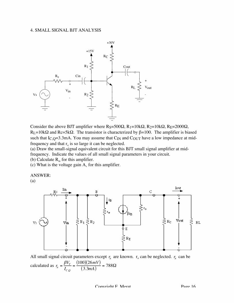
4. SMALL SIGNAL BJT ANALYSIS
RL
+30V
Cout
RE
RC
+15V
R1
R2
Cin
Vs
Rs
Vout
+
-Vin
+
-
Consider the above BJT amplifier where RS=500Ω, R1=10kΩ, R2=10kΩ, RE=2000Ω,RL=10kΩ and Rc=5kΩ. The transistor is characterized by β=100. The amplifier is biasedsuch that IC,Q=3.3mA. You may assume that CIN and COUT have a low impedance at mid-frequency and that ro is so large it can be neglected.(a) Draw the small-signal equivalent circuit for this BJT small signal amplifier at mid-frequency. Indicate the values of all small signal parameters in your circuit.(b) Calculate Rin for this amplifier.(c) What is the voltage gain Av for this amplifier.
ANSWER:(a)
All small signal circuit parameters except rπ are known. ro can be neglected. rπ can be
calculated as rπ =βVT
IC ,Q
=100( ) 26mV( )
3.3mA( )= 788Ω

Copyright F. Merat Page 17
(b) Normally you assume that the bias resistor equivalent resistance
RB = R1 ||R2 =R1( ) R2( )R1 + R2
=10kΩ( ) 10kΩ( )10kΩ+10kΩ
= 5kΩ is so large that it can be neglected. That was
not true in this problem since it is only 5000 ohms. We continue to use the definition of input
resistance Rin =Vin
Iin
. The input current is now calculated as Iin =Vin
R1 || R2
+ iB . The
corresponding input voltage can be calculated as Vin = iBrπ + β +1( )iB RE = iB rπ + β +1( )RE( ) .
Solving for iB gives iB =Vin
rπ + β +1( )RE
which can be substituted into the expression for Vin to
give Iin =Vin
R1 || R2
+Vin
rπ + β +1( )RE
. Using this expression in that for Rin gives
Rin =Vin
Iin
=Vin
Vin
R1 || R2
+Vin
rπ + β +1( )RE
=1
1
R1 || R2
+1
rπ + β +1( )RE
which can be recognized as
Rin = R1 || R2( ) || rπ + β +1( )RE( ) .
Numerically this gives Rin = 5kΩ( ) || 788 + 100 +1( )2000( ) = 5kΩ( ) || 202788Ω( ) = 4880Ω.
(c) Note that iB is independent of Rin and is given by iB =Vin
rπ + β +1( )RE
. The collector
current is then iC = βiB = βVin
rπ + β +1( )RE
=β
rπ + β +1( )RE
Vin . The output voltage is then
Vout = −iC RC || RL( ) = −β
rπ + β +1( )RE
Vin RC || RL( ) . Solving for the voltage gain gives
Vout
Vin
= −β RC || RL( )
rπ + β +1( )RE
.
Numerically,Vout
Vin
= −β RC || RL( )
rπ + β +1( )RE
= −100 5000Ω ||10000Ω( )788Ω + 100 +1( )2000Ω
= −1.64

Copyright F. Merat Page 18

Copyright F. Merat Page 19

Copyright F. Merat Page 20

Copyright F. Merat Page 21
Transistors - FETS

Copyright F. Merat Page 22

Copyright F. Merat Page 23

Copyright F. Merat Page 24

Copyright F. Merat Page 25

Copyright F. Merat Page 26
5. Biasing MOSFETsFor the MOSFET amplifier circuit shown below determine the DC operating point of thetransistor, i.e. determine ID, VDS, and VGS.
vs+-
Rgen
Ci
R1
R2
RD
VDD
RL
Co
vout
+
-
vout
The circuit uses the values Rgen= 10kΩ, VDD=18V, R1=3.3MΩ, R2=1.2MΩ, RD=2kΩ, andRL=5kΩ The MOSFET is characterized by K=0.96mA/V2 and VT=2.5 volts.
ANSWER:There is no voltage at the source as it is connected directly to ground. VGS is determined onlyby VG which is set by the R1-R2 voltage divider.
VGS =R2
R1 + R2
VDD =1.2MΩ
1.2MΩ + 3.3MΩ18V( ) = 0.27( ) 18V( ) = 4.8Volts
With the transistor parameter K AND VGS we can calculate the drain current as:
ID = K VG −VT( )2= 0.96
mAV 2 4.8V − 2.5V( )2
= 5.08mA
Once the drain current is known we can apply KVL to the loop from ground through thetransistor, through RD, and through the power supply to ground to get:VDS = VDD − IDRD =18 − 5.08mA( ) 2kΩ( ) = 7.84Volts

Copyright F. Merat Page 27

Copyright F. Merat Page 28

Copyright F. Merat Page 29
6. Small Signal Amplifier Analysis
Consider the above small signal equivalent circuit for a MOSFET amplifier. The circuitparameters are RSOURCE=100Ω, RB=1.5MΩ, RS=330Ω, and RL=100Ω. The transistor’s smallsignal parameters are gm=0.05S and rd=100kΩ.(a) Determine the small signal voltage gain of this amplifier.(b) What is the input impedance Rin of this amplifier? The output impedance Rout?(c) What is the current gain of this amplifier ASSUMING THAT Rin =200kohms,
Rout=1000ohms, and Vout
Vin
=1?
Answer:(a) Rd is so large compared to RS||RL that it can be neglected. Then
RL '= RS || RL =RSRL
RS + RL
=330Ω( ) 100Ω( )330Ω +100Ω
= 76.75Ω
In the output circuit Vout = + gmVGS( )RL '= + 0.05VGS( ) 76.75Ω( ) = 3.84VGS [1]
Using KVL around the input circuit gives −Vin +VGS + Vout = 0 . [2]
Substituting [1] into [2] gives −Vin +Vout
3.84+ Vout = 0 which can be solved to give the voltage
gain −Vin +1.26Vout = 0, or Vout
Vin
= +0.79
(b) By inspection. Rin=RB=1.5MΩUsing the definition for the output resistance and applying a test voltage source we get
Rout =VT
IT
=VT
VT
rd
+VT
RS
+ gmVT
= rd || RS ||1gm
After substituting values we have Rout = rd || RS ||1
gm
= 100kΩ || 330Ω ||20Ω ≅18.85Ω
(c)
Ai =iout
iin
=
VoutRout
VinRin
=Vout
Vin
Rin
Rout
= 1( )200kΩ1kΩ
= 200

Copyright F. Merat Page 30
3. MOSFETs (AC AMPLIFIER)The amplifier circuit shown below uses an enhancement mode MOSFET with k=2.7 mA/V2
and VT=2.5 volts operating at IDQ=1.2 mA. The circuit parameters are Rgen=600Ω,RK=1kΩ, RL=10kΩ, R1=1.285MΩ, and R2=237kΩ. You may neglect rd for the MOSFET.
(a) Draw a small signal equivalent circuit for this amplifier indicating the values of all smallsignal parameters. Note that RS is NOT bypassed.
(b) Derive an expression for the small signal gain Av =Vout
Vin
of this amplifier.
ANSWER:(a) The small signal model is
Vs+-
Rgen
Ci
R1
R2
RD
VDD
RL
Co +
-
Vout
RS
+
-
Vin

Copyright F. Merat Page 31
I combined R1 and R2 into the single bias resistor RG since both go to ground. All the circuitparamerers are known except for RG and gm from the previous circuit diagram. The bias
resistor is given by RG =R1R2
R1 + R2
=1285kΩ( ) 237kΩ( )
1285kΩ( ) + 237kΩ( )= 200kΩ. gm can be computed as
gm = 2 KIDQ = 2 2.7maV 2
⎛ ⎝
⎞ ⎠ 1.2mA( ) = 0.0036S
To determine the small voltage gain we first need to determine VGS. We can do KVL aroundthe loop defined by Vin, VGS and RS, i.e., −Vin +VGS + gmVGS( )RS = 0. This gives
VGS =Vin
1 + gmRS
. The output voltage is simply given as Vout = − gmVGS( ) RD || RL( ) . These two
results can be combined to give Vout = − gm( ) Vin
1 + gmRS
⎛
⎝ ⎜ ⎞
⎠ ⎟ RD || RL( ) or
Vout
Vin
= −gm
1 + gmRS
RD || RL( ) .

Copyright F. Merat Page 32
REFERENCE MATERIAL:
TRANSISTORS
MEASURED 2N2222 BJT CHARACTERISTICS
V (volts)CE
0 2 4 6 8 10 12 14 16 18 20
I = 35µAB
30 µA
25 µA
20 µA
15 µA
10 µA
5 µA
0
6
8
4
2
10
I (m
A)
C
MEASURED 2N5447 MOSFET CHARACTERISTICS
V (volts)DS
0 4 8 12 20 24 28 32 36 40
0
1.2
1.6
0.8
0.4
2.0
I -
Dra
in c
urre
nt (
amps
)D
16
V = 10 voltsGS9 volts
8 volts
7 volts
6 volts
5 volts
4 volts
3 volts
MOSFETs BJTsVT=26mV @ 300˚ C
ID = K VGS − VTO( )2
rπ =βVT
IC ,Q
gm = 2K VGS −VTO( ) = 2 KIDQ gm =βrπ
=IC,Q
VT